29
Scanning Tunneling Microscopy and Atomic Force Microscopy EEW508 Scanning probe microscopy
| Date post: | 01-Jan-2016 |
| Category: |
Documents |
| Upload: | blaze-phelps |
| View: | 88 times |
| Download: | 6 times |

Scanning Tunneling Microscopy and Atomic Force Microscopy
EEW508Scanning probe microscopy
Scanning Tunneling Microscopy (STM) - History - Principle of STM - Operation modes – constant current mode, constant height mode,
conductance mapping, tunneling spectroscopy - Examples of STM studies – atomic structures, dynamics, STM manipulation
Atomic Force Microscopy (AFM) - History - Principle of AFM - Operation modes – contact, non-contact, intermittent modes - Variation of AFM – friction force microscopy, conductive probe AFM,
electrostatic force microscopy, etc. - Examples of AFM studies – atomic stick-slip, friction, adhesion properties of
surfaces
EEW508Scanning probe microscopy

Beginning of Scanning Probe Microscopy
• Invention of scanning tunneling microscopy (1982)
• Gerd Binnig & Heine Rohrer, IBM Zurich (nobel prize in 1986)
First STM image of Si (7x7)Reconstruction on Si (111) surfacePhys Rev Lett (1983)
EEW508Scanning probe microscopy

Sample surface
Tunneling current (I)
d
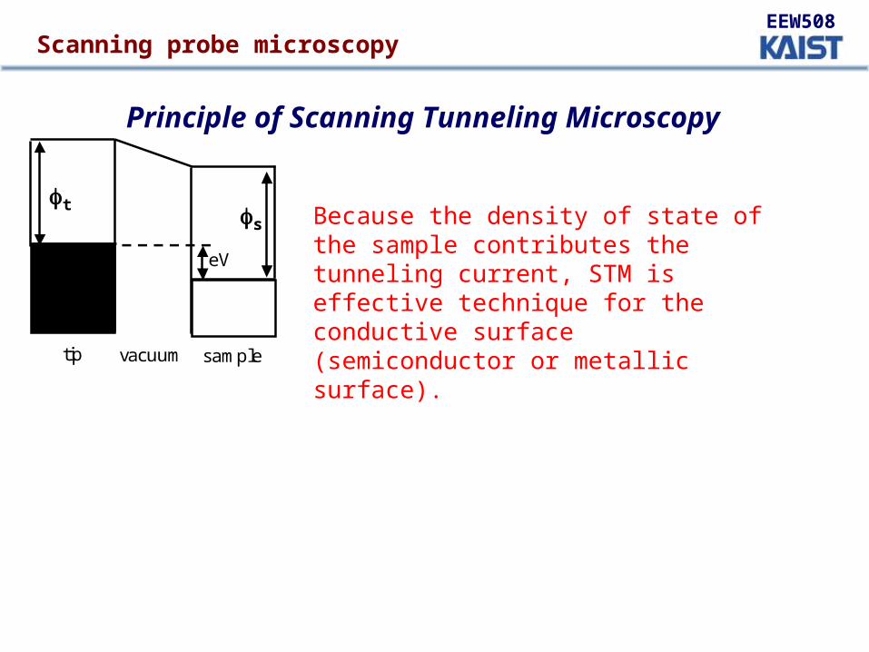
Principle of Scanning Tunneling Microscopy
STM tip
I ~ e –2d
(d: tip-sample separation, K is the
constant)
A
V
I
The key process in STM is the quantum tunneling of electrons through a thin potential barrier separating two electrodes. By applying a voltage (V) between the tip and a metallic or semiconducting sample, a current can flow (I) between these electrodes when their distance is reduced to a few atomic diameters.
EEW508Scanning probe microscopy
Principle of Scanning Tunneling Microscopy
Because the density of state of the sample contributes the tunneling current, STM is effective technique for the conductive surface (semiconductor or metallic surface).
tip samplevacuum
eV
t s
EEW508Scanning probe microscopy
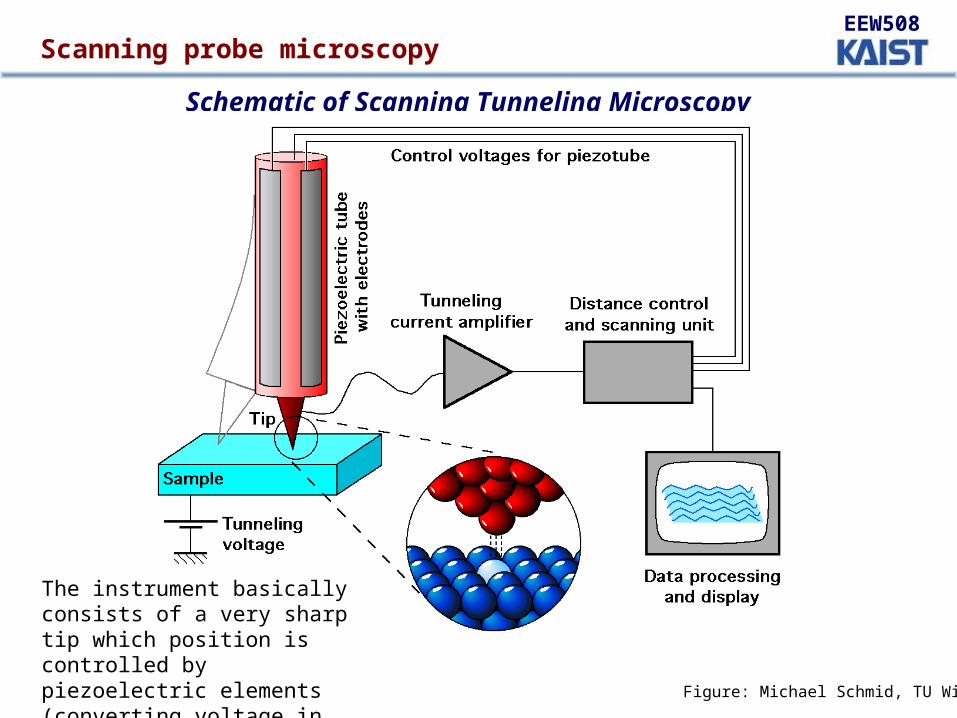
Schematic of Scanning Tunneling Microscopy
Figure: Michael Schmid, TU Wien
The instrument basically consists of a very sharp tip which position is controlled by piezoelectric elements (converting voltage in mechanical deformation)
EEW508Scanning probe microscopy
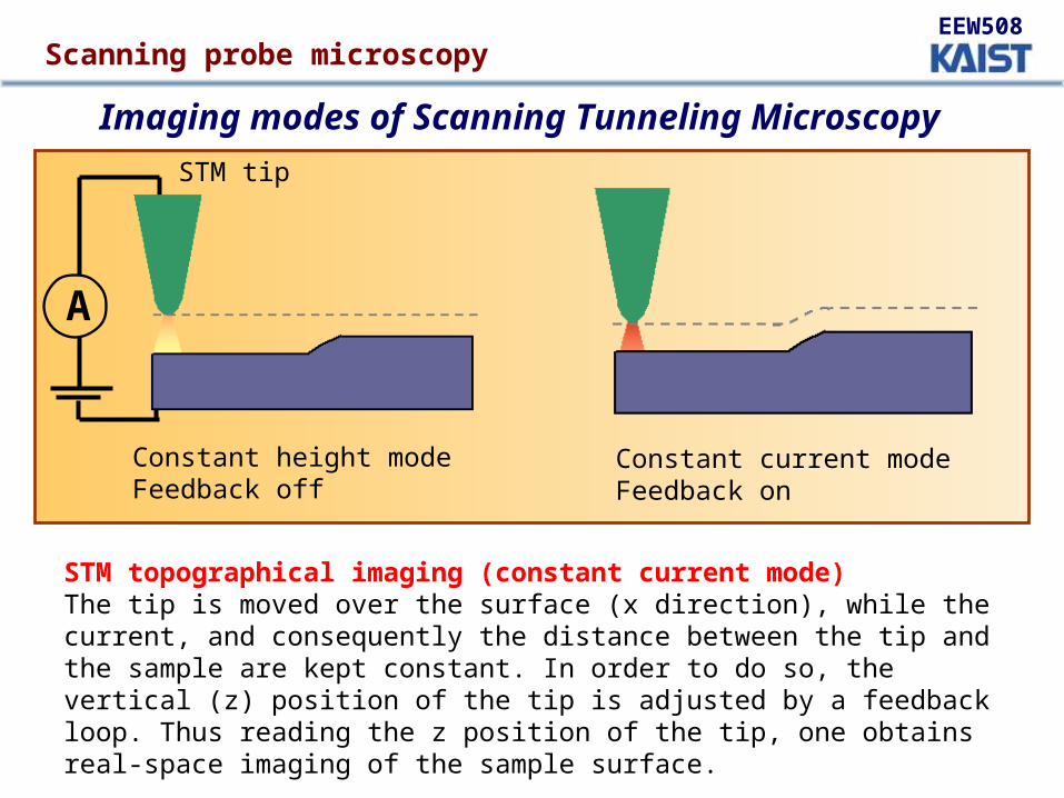
Constant height modeFeedback off
A
Constant current modeFeedback on
STM tip
Imaging modes of Scanning Tunneling Microscopy
STM topographical imaging (constant current mode)The tip is moved over the surface (x direction), while the current, and consequently the distance between the tip and the sample are kept constant. In order to do so, the vertical (z) position of the tip is adjusted by a feedback loop. Thus reading the z position of the tip, one obtains real-space imaging of the sample surface.
EEW508Scanning probe microscopy

Scanning Tunneling Spectroscopy
(M. Crommie group)
Silicon (100) (2x1) dimer row reconstruction structure
1
2
3
4
5
6
-3 -2 -1 0 1 2 3sample voltage(V)
dI/d
V/(
I/V)
Tunneling spectroscopy reveals the bandgap of 0.7 eV due to the presence of surface states
EEW508Scanning probe microscopy
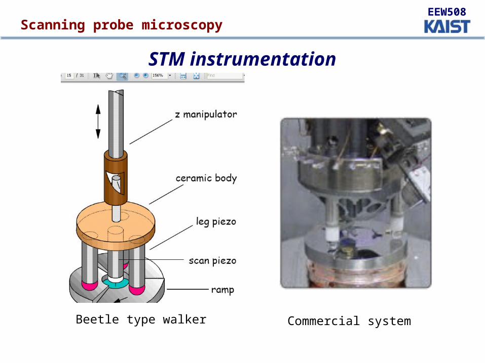
STM instrumentation
Beetle type walker Commercial system
EEW508Scanning probe microscopy

Examples of STM studies1. Atomic manipulation (Don Eigler, IBM)
Quantum corral (D. Eigler)
Xe atoms on Ni (100) at 8Kassembled by atomic manipulation
Iron on Copper (111) assembled by atomic manipulation
A node in the electron standing wave
Fe atoms
EEW508Scanning probe microscopy
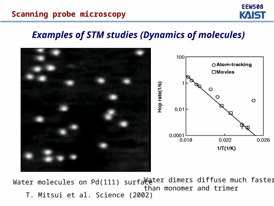
Examples of STM studies (Dynamics of molecules)
Water molecules on Pd(111) surface Water dimers diffuse much faster than monomer and trimer
T. Mitsui et al. Science (2002)
EEW508Scanning probe microscopy
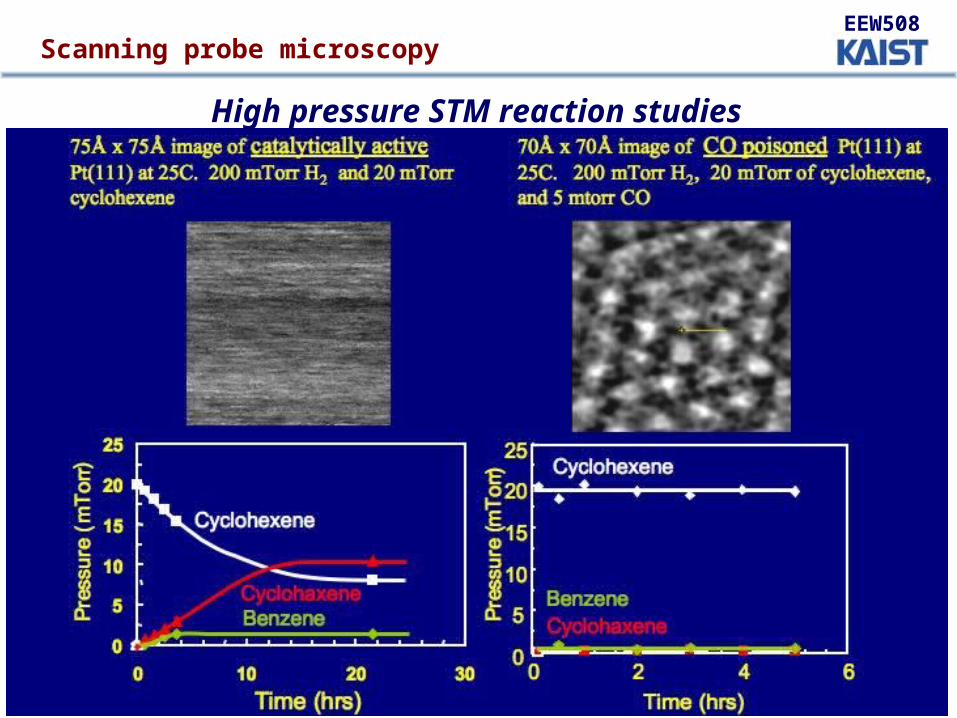
(Somorjai group) High pressure STM reaction studies
EEW508Scanning probe microscopy
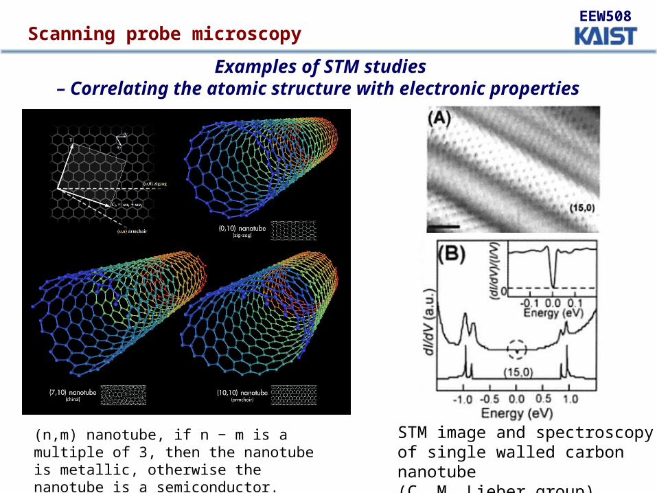
Examples of STM studies – Correlating the atomic structure with electronic properties
STM image and spectroscopy of single walled carbon nanotube (C. M. Lieber group)
(n,m) nanotube, if n − m is a multiple of 3, then the nanotube is metallic, otherwise the nanotube is a semiconductor.
EEW508Scanning probe microscopy
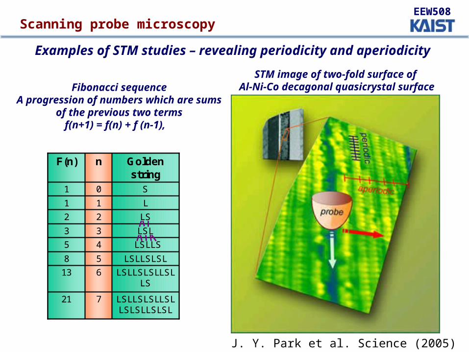
Examples of STM studies – revealing periodicity and aperiodicity
J. Y. Park et al. Science (2005)
LSLLSLSLLSLLSLSLLSLSL
721
LSLLSLSLLSLLS
613
LSLLSLSL58
LSLLS45
LSL33
LS22
L11
S01
Golden string
nF(n)
LSLLSLSLLSLLSLSLLSLSL
721
LSLLSLSLLSLLS
613
LSLLSLSL58
LSLLS45
LSL33
LS22
L11
S01
Golden string
nF(n)
Fibonacci sequenceA progression of numbers which are
sums of the previous two termsf(n+1) = f(n) + f (n-1),
STM image of two-fold surface of Al-Ni-Co decagonal quasicrystal surface
EEW508Scanning probe microscopy
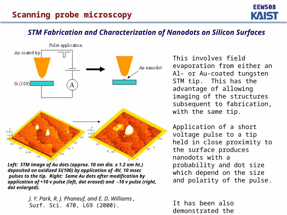
STM Fabrication and Characterization of Nanodots on Silicon Surfaces
This involves field evaporation from either an Al- or Au-coated tungsten STM tip. This has the advantage of allowing imaging of the structures subsequent to fabrication, with the same tip.
Application of a short voltage pulse to a tip held in close proximity to the surface produces nanodots with a probability and dot size which depend on the size and polarity of the pulse.
It has been also demonstrated the modification of existing nanodots, via the application of additional, larger voltage pulses of both polarities. J. Y. Park, R. J. Phaneuf, and E. D. Williams,
Surf. Sci. 470, L69 (2000).
Left: STM image of Au dots (approx. 10 nm dia. x 1.2 nm ht.) deposited on oxidized Si(100) by application of -8V, 10 msec pulses to the tip. Right: Same Au dots after modification by application of +10 v pulse (left, dot erased) and –10 v pulse (right, dot enlarged).
EEW508Scanning probe microscopy
Atomic Force Microscopy
EEW508Scanning probe microscopy
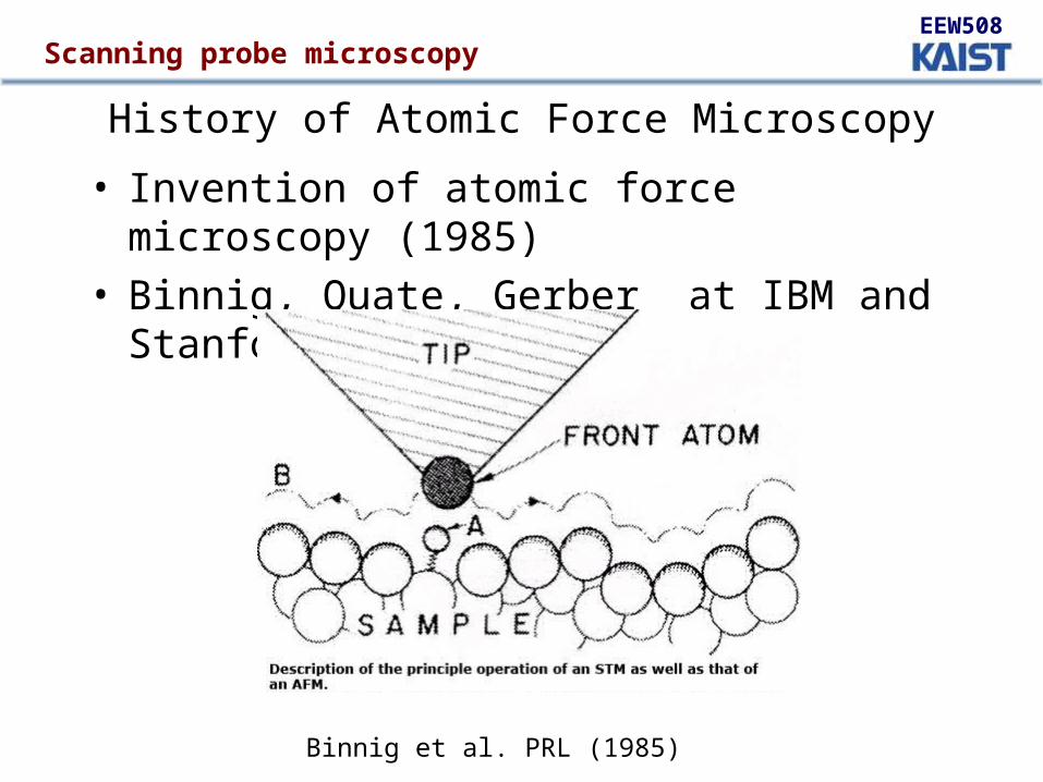
History of Atomic Force Microscopy
• Invention of atomic force microscopy (1985)• Binnig, Quate, Gerber at IBM and Stanford
Binnig et al. PRL (1985)
EEW508Scanning probe microscopy
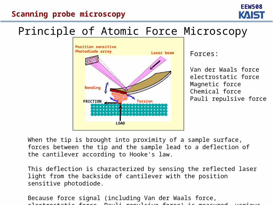
Position sensitive Photodiode array Laser beam
Bending
Torsion
LOAD
FRICTION
Principle of Atomic Force Microscopy
When the tip is brought into proximity of a sample surface, forces between the tip and the sample lead to a deflection of the cantilever according to Hooke's law.
This deflection is characterized by sensing the reflected laser light from the backside of cantilever with the position sensitive photodiode.
Because force signal (including Van der Waals force, electrostatic force, Pauli repulsive force) is measured, various samples including insulator can be imaged in AFM.
EEW508Scanning probe microscopy
Forces:
Van der Waals forceelectrostatic forceMagnetic forceChemical forcePauli repulsive force
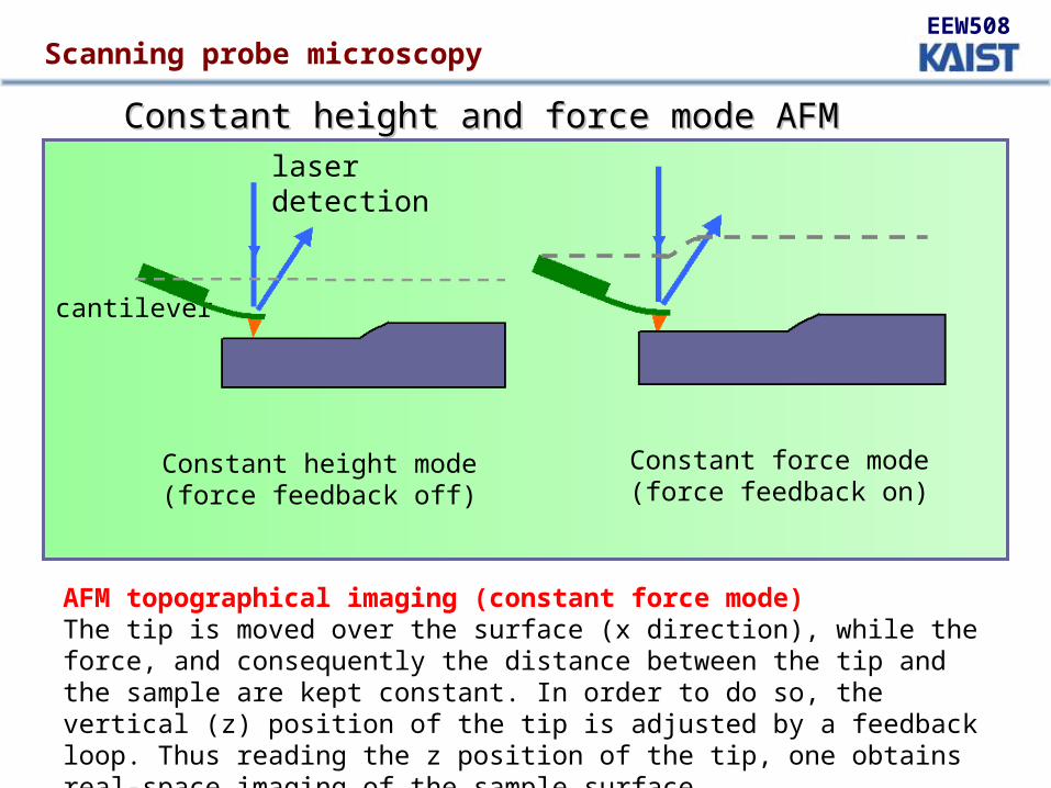
Constant height mode(force feedback off)
Constant force mode(force feedback on)
laserdetection
cantilever
Constant height and force mode AFMConstant height and force mode AFM
AFM topographical imaging (constant force mode)The tip is moved over the surface (x direction), while the force, and consequently the distance between the tip and the sample are kept constant. In order to do so, the vertical (z) position of the tip is adjusted by a feedback loop. Thus reading the z position of the tip, one obtains real-space imaging of the sample surface.
EEW508Scanning probe microscopy
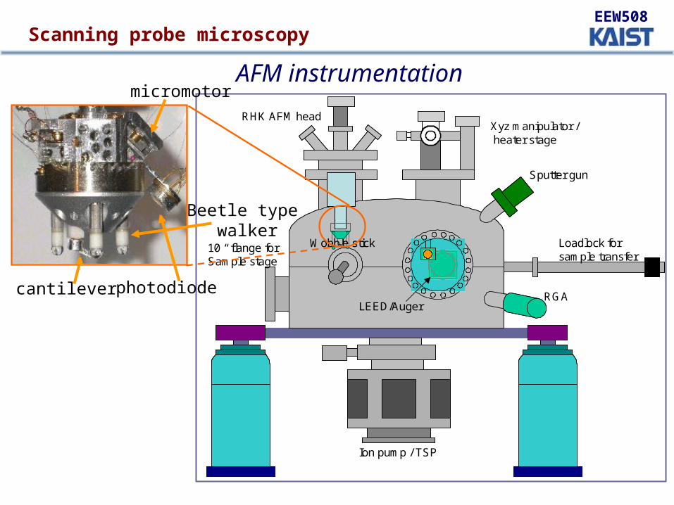
Ion pump / TSP
RHK AFM headXyz manipulator /heater stage
Sputter gun
RGA
Loadlock for sample transfer
LEED/Auger
Wobble stick10 “ flange forSample stage
micromotor
photodiode
Beetle type walker
cantilever
AFM instrumentation
EEW508Scanning probe microscopy
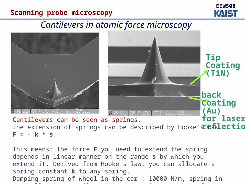
Tip Coating(TiN)
back Coating(Au)for laser reflection
Cantilevers in atomic force microscopy
Cantilevers can be seen as springs.the extension of springs can be described by Hooke's Law F = - k * s.
This means: The force F you need to extend the spring depends in linear manner on the range s by which you extend it. Derived from Hooke's law, you can allocate a spring constant k to any spring. Damping spring of wheel in the car : 10000 N/m, spring in the ball point pencil : 1000 N/m, spring constant of commercial cantilever :0.01 – 100 N/m
EEW508Scanning probe microscopy
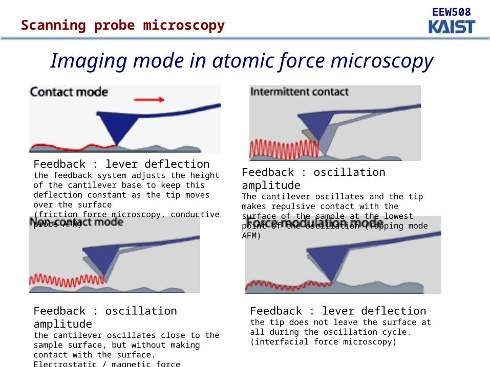
Imaging mode in atomic force microscopy
Feedback : lever deflectionthe feedback system adjusts the height of the cantilever base to keep this deflection constant as the tip moves over the surface(friction force microscopy, conductive probe AFM)
Feedback : oscillation amplitudeThe cantilever oscillates and the tip makes repulsive contact with the surface of the sample at the lowest point of the oscillation (Tapping mode AFM)
Feedback : oscillation amplitudethe cantilever oscillates close to the sample surface, but without making contact with the surface. Electrostatic / magnetic force microscopy
Feedback : lever deflectionthe tip does not leave the surface at all during the oscillation cycle. (interfacial force microscopy)
EEW508Scanning probe microscopy
AB
DC
AB
DC
AB
DC
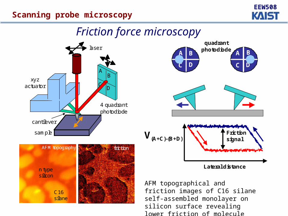
xyz actuator
4 quadrant photodiode
laser
cantilever
sample V(A+C)-(B+D)
Lateral distance
quadrantphotodiode
Friction signal
A B
C D
A B
C D
Friction force microscopy
AFM topography friction
C16 silane
n typesilicon
AFM topographical and friction images of C16 silane self-assembled monolayer on silicon surface revealing lower friction of molecule layers
EEW508Scanning probe microscopy
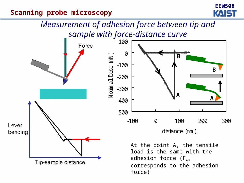
Measurement of adhesion force between tip and sample with force-distance curve
-500
-400
-300
-200
-100
0
100
-100 0 100 200 300
distance (nm)
No
rmal
for
ce (
nN)
A
B
A
B
At the point A, the tensile load is the same with the adhesion force (FAB corresponds to the adhesion force)
EEW508Scanning probe microscopy
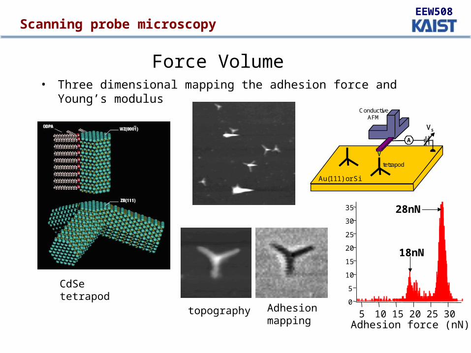
Force Volume Mapping• Three dimensional mapping the adhesion force and Young’s
modulus
CdSe tetrapod
Adhesion force (nN)
35
30
25
20
15
10
5
0
30252015105
18nN
28nN
ConductiveAFM
Au(111) or Si
A
Vs
A
Vs
tetrapod
topography Adhesion mapping
EEW508Scanning probe microscopy

AFM images of various materials
Contact mode AFM topography (left), friction (right) images of graphite surface
Contact mode friction image (left) and its line profile of mica surface which show atomic stick-slip process
Contact mode topographical (up) and friction images (bottom) of polymer
EEW508Scanning probe microscopy
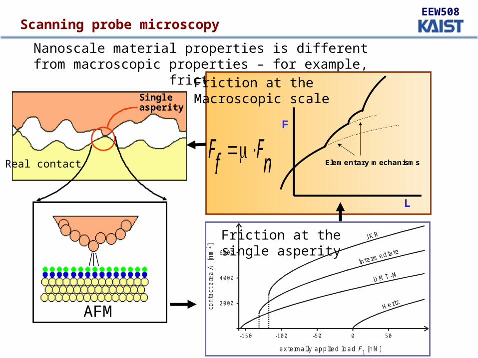
Nanoscale material properties is different from macroscopic properties – for example, friction
Singleasperity
Real contact
AFM cont
act
are
a
[nm
]
A2
-150
externally applied load [nN]Fl
-100 -50 0 50
2000
4000
6000
Friction at the single asperity
Friction at the Macroscopic scale
Ff
Fn
F
L
Elementary mechanisms
EEW508Scanning probe microscopy
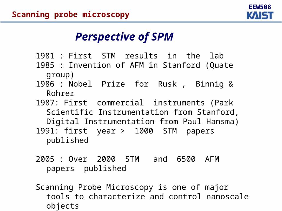
1981 : First STM results in the lab1985 : Invention of AFM in Stanford (Quate group)1986 : Nobel Prize for Rusk , Binnig & Rohrer1987: First commercial instruments (Park Scientific
Instrumentation from Stanford, Digital Instrumentation from Paul Hansma)
1991: first year > 1000 STM papers published
2005 : Over 2000 STM and 6500 AFM papers published
Scanning Probe Microscopy is one of major tools to characterize and control nanoscale objects
Perspective of SPM
EEW508Scanning probe microscopy
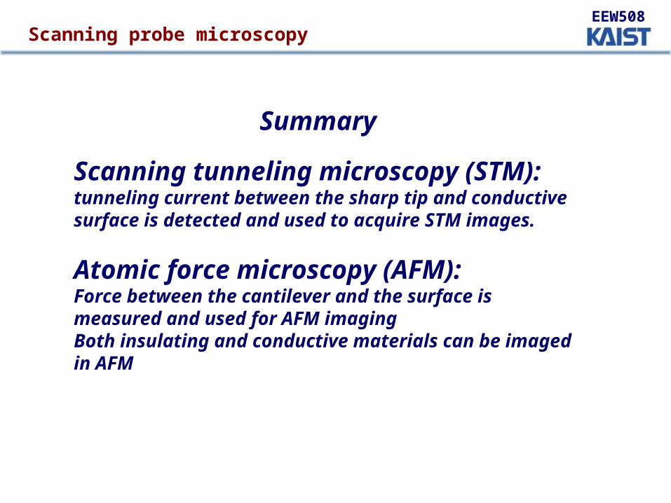
Summary
Scanning tunneling microscopy (STM): tunneling current between the sharp tip and conductive surface is detected and used to acquire STM images.
Atomic force microscopy (AFM): Force between the cantilever and the surface is measured and used for AFM imaging Both insulating and conductive materials can be imaged in AFM
EEW508Scanning probe microscopy


