Page 1
SCANNING TUNNELING MICROSCOPY STUDIES OF FLUORINATED GRAPHENE
FILMS AND FIELD-DIRECTED SPUTTER SHARPENING
BY
SCOTT W. SCHMUCKER
DISSERTATION
Submitted in partial fulfillment of the requirements
for the degree of Doctor of Philosophy in Electrical and Computer Engineering
in the Graduate College of the
University of Illinois at Urbana-Champaign, 2012
Urbana, Illinois
Doctoral Committee:
Professor Joseph W. Lyding, Chair
Professor John R. Abelson
Professor James J. Coleman
Assistant Professor Eric Pop
Page 2
ii
ABSTRACT
Graphene fluoride is a two-dimensional fluorocarbon, and the wide-gap analogue of
graphene. Among chemical derivatives of graphene, graphene fluoride is unique in its ease of
synthesis and stability, as well as the extensive study of its bulk form, graphite fluoride. Only in
the last few years, however, has graphene fluoride been isolated experimentally, and our
understanding of its atomic and electronic structure, stability, reduction, and use as a platform for
lithographic patterning is still limited. In this dissertation, an ultra-high vacuum scanning
tunneling microscope (UHV-STM) is employed for the characterization of exfoliated double-
sided graphene fluoride (ds-GF) and of single-sided graphene fluoride (ss-GF) on Cu foil. We
explore the structure and stability of each material and, in particular, identify ss-GF as a stable,
well-ordered, wide-gap semiconductor. This dissertation offers the first atomic-resolution study
of this novel material, and the first UHV-STM measurement of its electronic structure.
Furthermore, we develop the novel field-directed sputter sharpening (FDSS) technique
for producing sharp metal probes with 1 – 5 nm radii of curvature, a prerequisite for high-
resolution scanning tunneling microscopy (STM) imaging and nanolithography. We show that
FDSS offers significant improvements in lithographic patterning, and is applicable to a range of
materials, including the hard metallic-ceramic hafnium diboride (HfB2). Finally, we explore the
use of HfB2-coated W wires for STM imaging and spectroscopy.
Page 3
iii
ACKNOWLEDGEMENTS
My tenure at the University of Illinois has been formative, in large part due to the
uniquely inspiring atmosphere cultivated by Professor Joseph Lyding. I thank Joe for his
guidance and insight, but also for the freedom he has given me to work creatively and
collaboratively and to take an active role in choosing and developing my research program. It
remains a joy to work with Joe and to develop as a researcher both through individual
perseverance and from Joe’s extensive experience and keen insight.
My days in the Illinois STM group might have proven unproductive without the
camaraderie and support of my fellow sojourners. Among these, I would first thank those
students and researchers who assisted directly with the completion of this dissertation. My work
on field-directed sputter sharpening was enabled through collaboration with Navneet Kumar,
Scott Daly, Aditya Gupta, Daniel Lukman, and Eric Lee. Navneet provided his expertise and
time to deposit thin films of HfB2 onto tungsten STM tips under the guidance of Professor John
Abelson. Scott was the adept chemist who synthesized the Hf(BH4)4 precursor molecules in the
lab of Professor Greg Girolami. Aditya and Daniel both worked in the Lyding STM Lab as
undergraduate student researchers, and Eric Lee completed his M.S. degree while studying
plasma-based sputter sharpening of STM tips. Studies of fluorinated graphene in all its forms
were made possible only with the assistance of Josh Wood, Yang Liu, Dr. Chad Junkermeier,
and Dr. Rick Haasch. Yang and Professor T.-C. Chiang’s expertise in angle-resolved
photoelectron spectroscopy, and willingness to contribute of their valuable beam time are
appreciated, and added greatly to the impact of my studies. I was thrilled to meet Chad at the
APS March meeting in 2011 where I learned of his theoretical treatment of fluorinated graphene.
His computational support of this dissertation has been extremely valuable and provided a
Page 4
iv
substantial theoretical basis for my understanding of single-sided graphene fluoride. Rick’s
expertise in X-ray photoelectron spectroscopy was invaluable for characterizing samples, and his
assistance with data analysis and tolerance of my wandering into his lab with questions or new
samples is appreciated. Additionally, I am indebted to Dr. Matt Sztelle for his guidance in the
mysterious ways of UHV systems and lab operations, as well as his pasta sauce and many games
of racquetball. Dr. Laura Ruppalt offered her valuable knowledge of the “Chamber A” system
and trained me on its use. Kevin He helped to maintain Chamber A, and it has been a pleasure to
converse with him on subjects ranging from electron tunneling and general relativity to monetary
policy and chess. Josh Wood has been a valued colleague not only for his involvement in my
studies of graphene fluoride and his expertise in graphene CVD and Raman spectroscopy, but
also his passion for knowledge and hard work. I also thank Lea Neinhaus for her assistance in
reading and understanding the early studies of fluorinated graphene, published in German. No
member of the Lyding STM Lab has left without imparting useful knowledge to me, and I thank
all current and former lab members for their contributions to my development: Dr. Peter
Albrecht, Dr. Josh Ballard, Dr. Erin Carmichael, Dr. Kyle Ritter, Dr. Greg Scott, Sumit
Ashketar, Yaofeng Chen, Jae Won Do, Kyong Hee Joo, Justin Koepke, Ximeng Liu, Pam
Martin, Marie Mayer, Vineet Nazareth, Peter Ong, Adrian Radocea, Alan Rudwick, Aditya
Vaidya, Bryan Walker, Wei Ye, and Fan Zhang.
Several other members of the Illinois community played integral roles in the success of
my research program. Specifically, Scott Robinson and Cate Wallace have repeatedly
contributed their expertise and enthusiasm for the transmission electron microscopy system
employed in this dissertation. The Imaging Technology Group of the Beckman Institute at the
University of Illinois maintains an excellent microscopy facility which has proven invaluable in
Page 5
v
the completion of my research. I have counted continually on the assistance and guidance of
staff members in the Frederick Seitz Materials Research Laboratory throughout the course of my
research, including Jim Mabon, Bharat Sankaran, Mike Marshall, and Tony Banks. Also, the
expert machining skills of Craig Zeilenga and Scott MacDonald have been poured into much of
the equipment of the Lyding lab. Our group secretary, Kelly Young, and storeroom manager,
Suzie Rook, of the Beckman Institute have contributed continually to the successful operation of
the laboratory.
I was privileged to spend several years as a teaching assistant in the ECE 444
undergraduate integrated circuit laboratory. I thank the lab director Professor Jim Coleman and
lab engineer Dane Sievers for their work in making this course available to students at the
University of Illinois, and in particular Dane for his insight into the maintenance and operation of
the clean room laboratory and integrated equipment. I hope that I can bring some of his insights
and inspirations with me into my career.
Additionally, I acknowledge the members of the Fermi Pinning bowling team, Josh
Wood, Justin Koepke, Albert Liao, and Joe Lyding. Competing in the annual ECE Strike
bowling tournament offered a welcome respite from the drudgeries of graduate school.
For all of their help to those of us seeking knowledge, I thank the staff of the University
of Illinois library system, especially those who like to read the acknowledgements in the new
theses. Yes, I mean you.
This dissertation would not have been possible without financial support, and I gratefully
acknowledge the assistance of a National Defense Science and Engineering Graduate Fellowship
from the Air Force Office of Scientific Research (2004 – 2007), and the National Science
Foundation Graduate Research Fellowship (2007 – 2009). This research was further funded by
Page 6
vi
the Office of Naval Research under grant number N000140610120 and the Defense Advanced
Research Project Agency and Space and Naval Warfare Center, San Diego under contract
N66001-08-C-2040.
I thank my parents, my sister April, my beloved daughter Lydia, and my family and
friends for their love and support in this and in all things. Finally, I thank my wife Christine. As
my life and burdens are shared with her, so too is this dissertation, as are all my works.
Page 7
vii
TABLE OF CONTENTS
CHAPTER 1: INTRODUCTION ................................................................................................ 1
1.1 Motivation ............................................................................................................. 1
1.2 Probe Sharpening Methodology ........................................................................... 3
1.3 Sputter Erosion Physics ........................................................................................ 7
1.4 Sputter Sharpening Apparatus ............................................................................ 10
1.5 Electron-Stimulated Desorption.......................................................................... 12
1.6 Hafnium Diboride ............................................................................................... 14
1.7 Graphene ............................................................................................................. 15
1.8 Fluorinated Graphite ........................................................................................... 21
1.9 Chemically Modified Graphene .......................................................................... 27
1.10 Graphene Growth and Fluorination Apparatus ................................................... 36
1.11 Thesis Statement ................................................................................................. 37
1.12 Figures................................................................................................................. 38
CHAPTER 2: FIELD-DIRECTED SPUTTER SHARPENING ............................................... 45
2.1 Field-Directed Sputter Sharpening ..................................................................... 45
2.2 Sharpening of Platinum Iridium Alloy Probes.................................................... 46
2.3 Sharpening of Tungsten Probes ........................................................................... 48
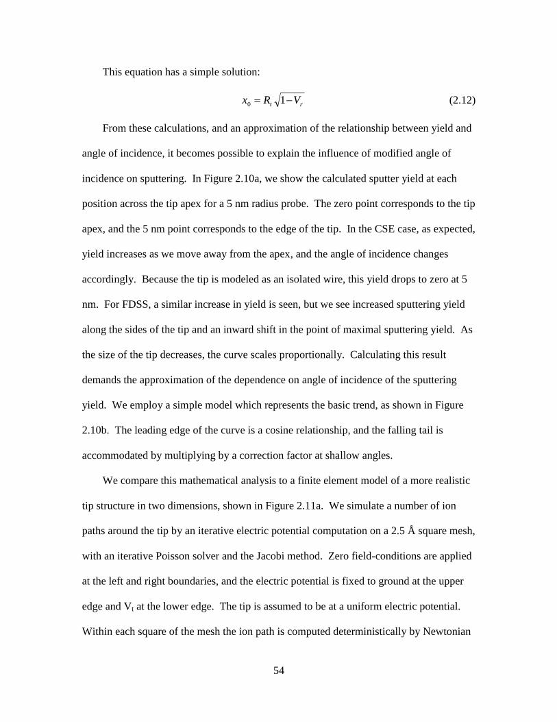
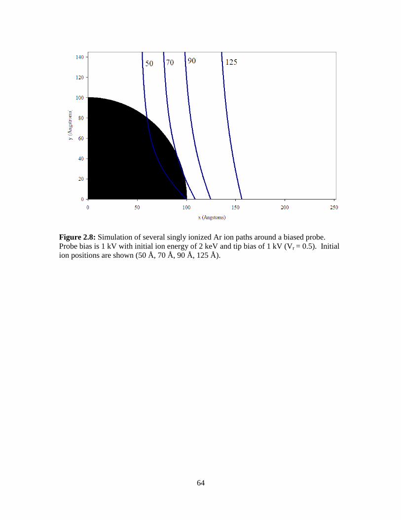
2.4 Off-Axis Sputter Erosion Sharpening ................................................................. 48
2.5 Sharpening of Diamond-Like Carbon Probes ..................................................... 49
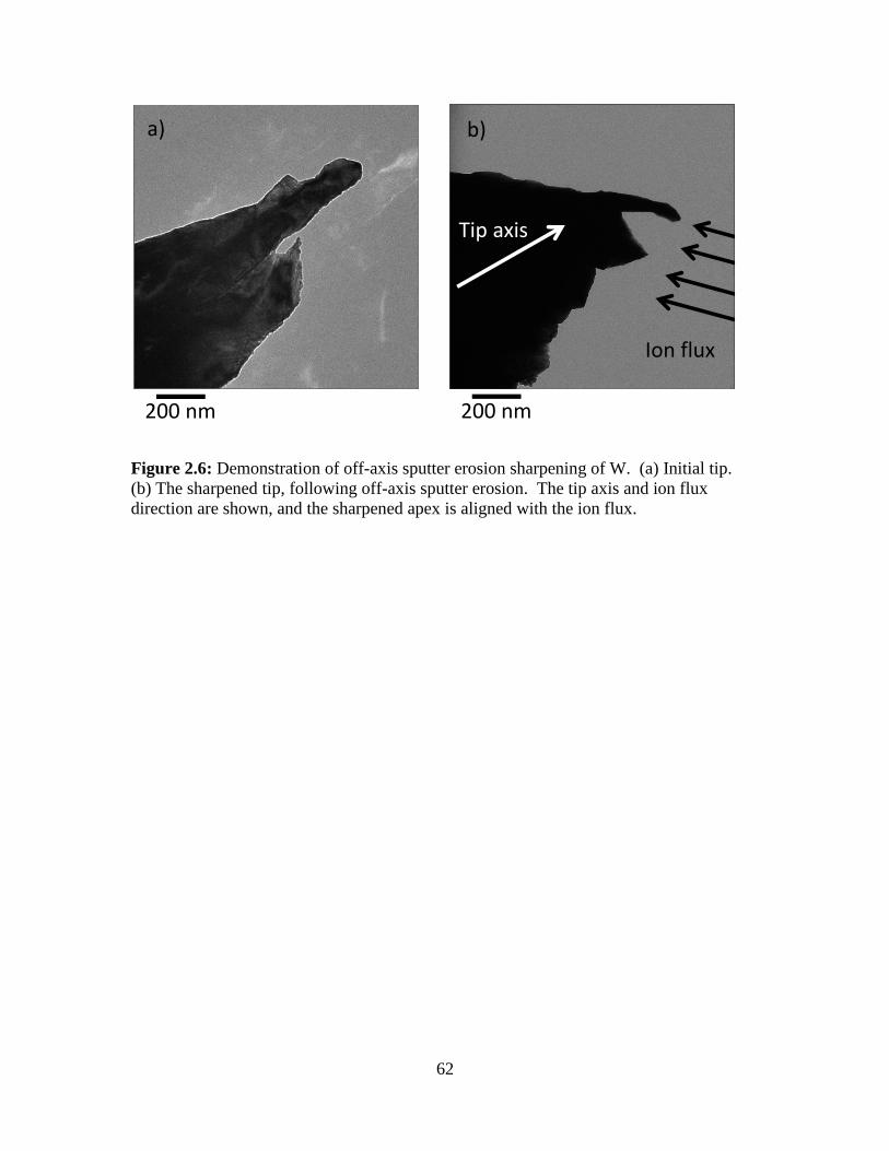
2.6 Simulation of Field-Directed Sputter Sharpening ............................................... 51
2.7 Discussion ........................................................................................................... 56
2.8 Figures ................................................................................................................. 57
CHAPTER 3: HAFNIUM DIBORIDE AS A PROBE MATERIAL FOR SCANNING
TUNNELING MICROSCOPY .......................................................................... 69
3.1 Hafnium Diboride Chemical Vapor Deposition ................................................. 70
3.2 Coating and Field-Directed Sputter Sharpening: Hafnium Diboride ................. 70
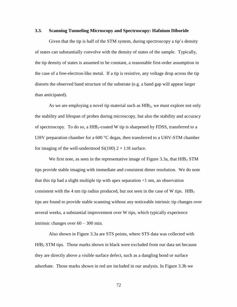
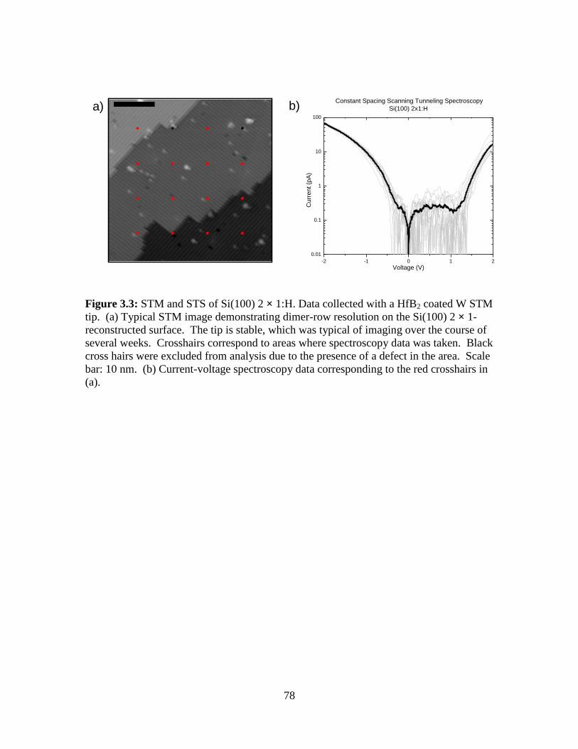
3.3 Scanning Tunneling Microscopy and Spectroscopy: Hafnium Diboride ........... 72
3.4 Discussion ........................................................................................................... 74
3.5 Figures................................................................................................................. 76
CHAPTER 4: SCANNING TUNNELING MICROSCOPY AND HIGH-FIDELITY
ELECTRON-STIMULATED DESORPTION ................................................... 80
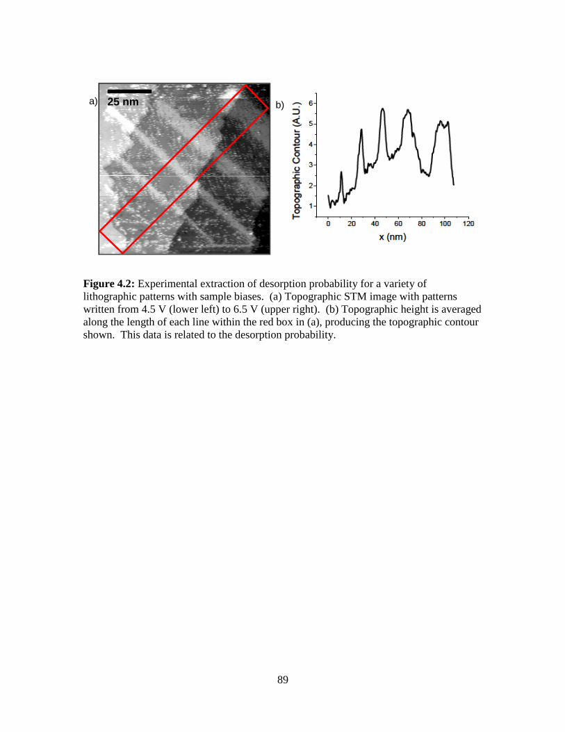
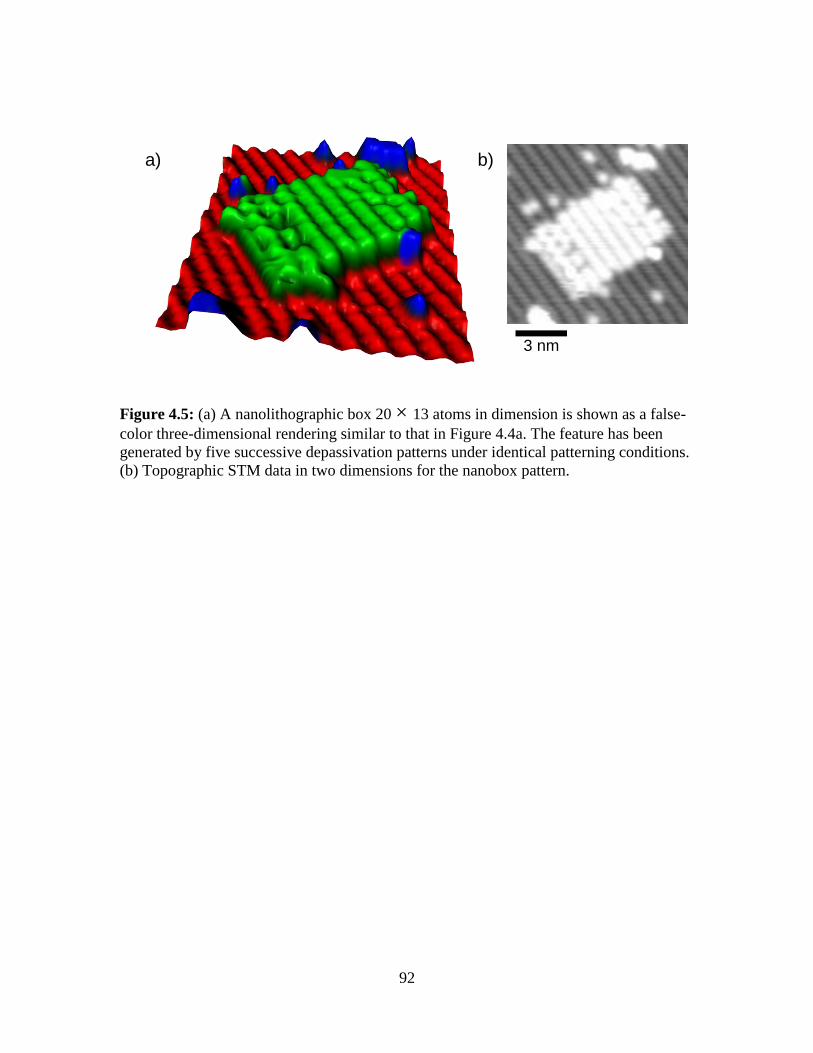
4.1 High-Fidelity Patterning of the Si(100) 2 × 1:H Surface .................................... 80
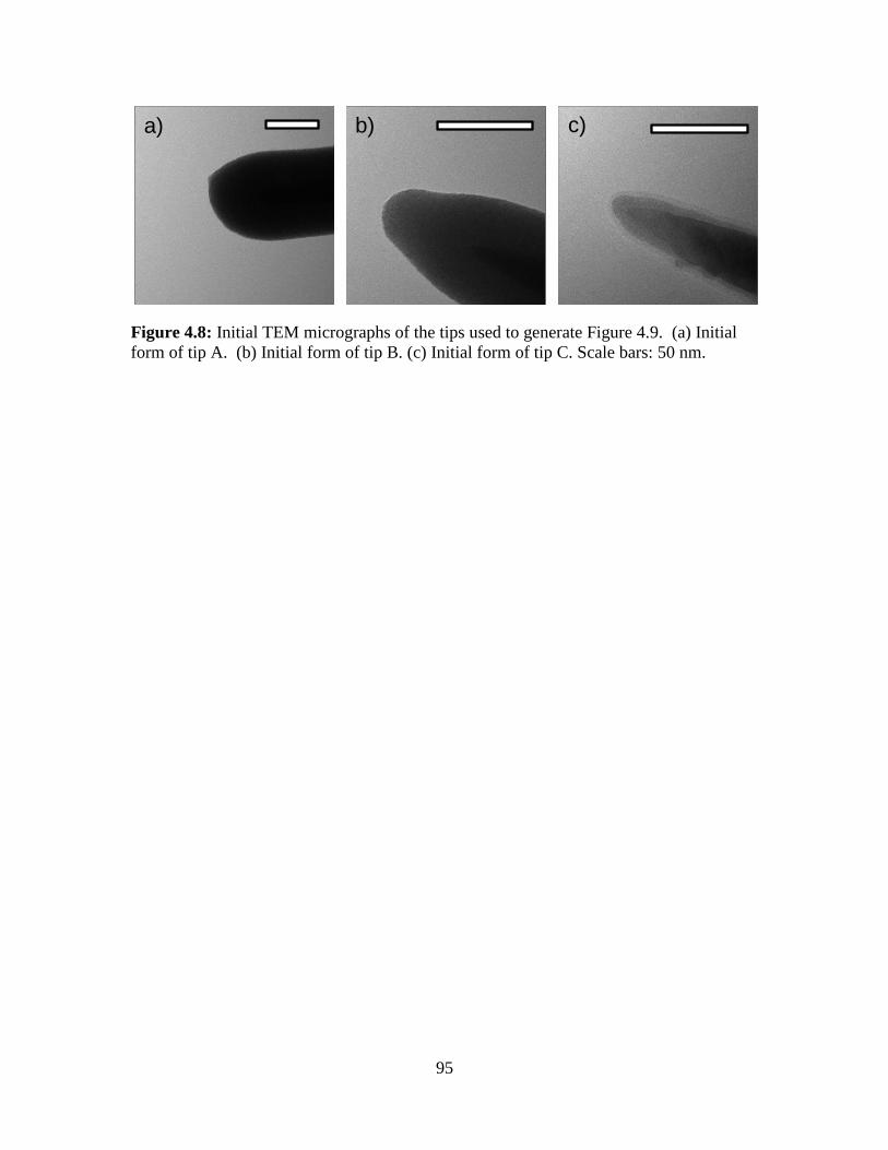
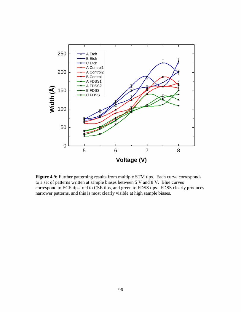
4.2 Influence of Field-Directed Sputter Sharpening on Patterning........................... 83
4.3 Probe Regeneration by Field-Directed Sputter Sharpening ................................ 85
4.4 Discussion ........................................................................................................... 87
4.5 Figures................................................................................................................. 88
Page 8
viii
CHAPTER 5: EXFOLIATION AND DECOMPOSITION OF PUCKERED-SHEET
GRAPHITE FLUORIDE .................................................................................... 99
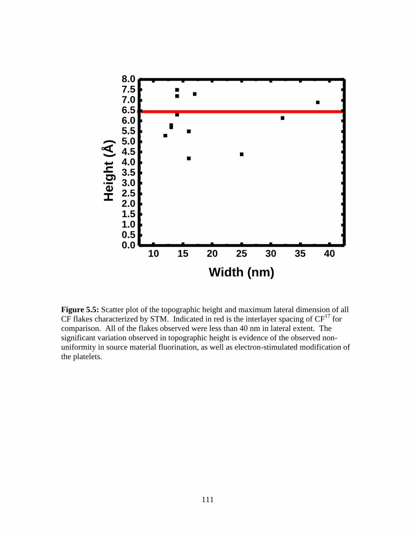
5.1 Characterization of Bulk Exfoliated Graphite Fluoride .................................... 100
5.2 Dry Contact Transfer of Puckered-Sheet Graphite Fluoride ............................ 101
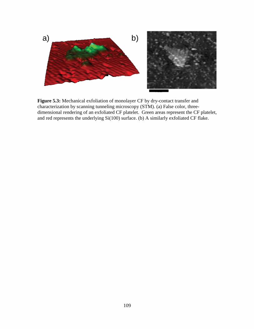
5.3 Scanning Tunneling Microscopy: Monolayer Fluorinated Graphene .............. 102
5.4 Electron-Stimulated Decomposition: Monolayer Fluorinated Graphene ......... 103
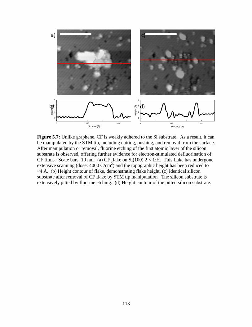
5.5 Defluorination and Silicon Substrate Etching................................................... 104
5.6 Discussion ......................................................................................................... 105
5.7 Figures............................................................................................................... 107
CHAPTER 6: ATOMIC AND ELECTRONIC STRUCTURE OF SINGLE-SIDED
GRAPHENE FLUORIDE ................................................................................ 114
6.1 X-ray Photoelectron Spectroscopy and Influence of Annealing....................... 115
6.2 Scanning Tunneling Microscopy: Order in Graphene Fluoride ....................... 116
6.3 Scanning Tunneling Spectroscopy: Graphene Fluoride Band Structure .......... 119
6.4 Discussion ......................................................................................................... 121
6.5 Figures............................................................................................................... 122
CHAPTER 7: CONCLUSIONS AND FUTURE WORK ........................................................ 135
7.1 Dissertation Summary ....................................................................................... 135
7.2 Future Work ...................................................................................................... 137
REFERENCES ......................................................................................................................... 139
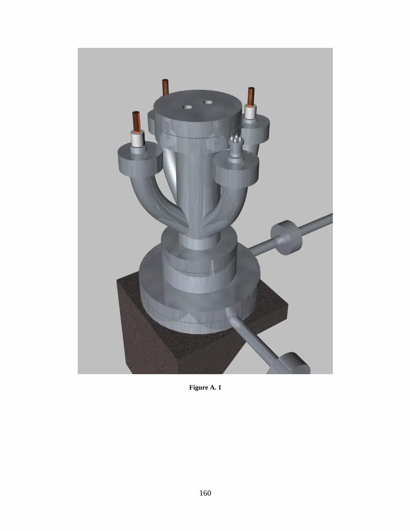
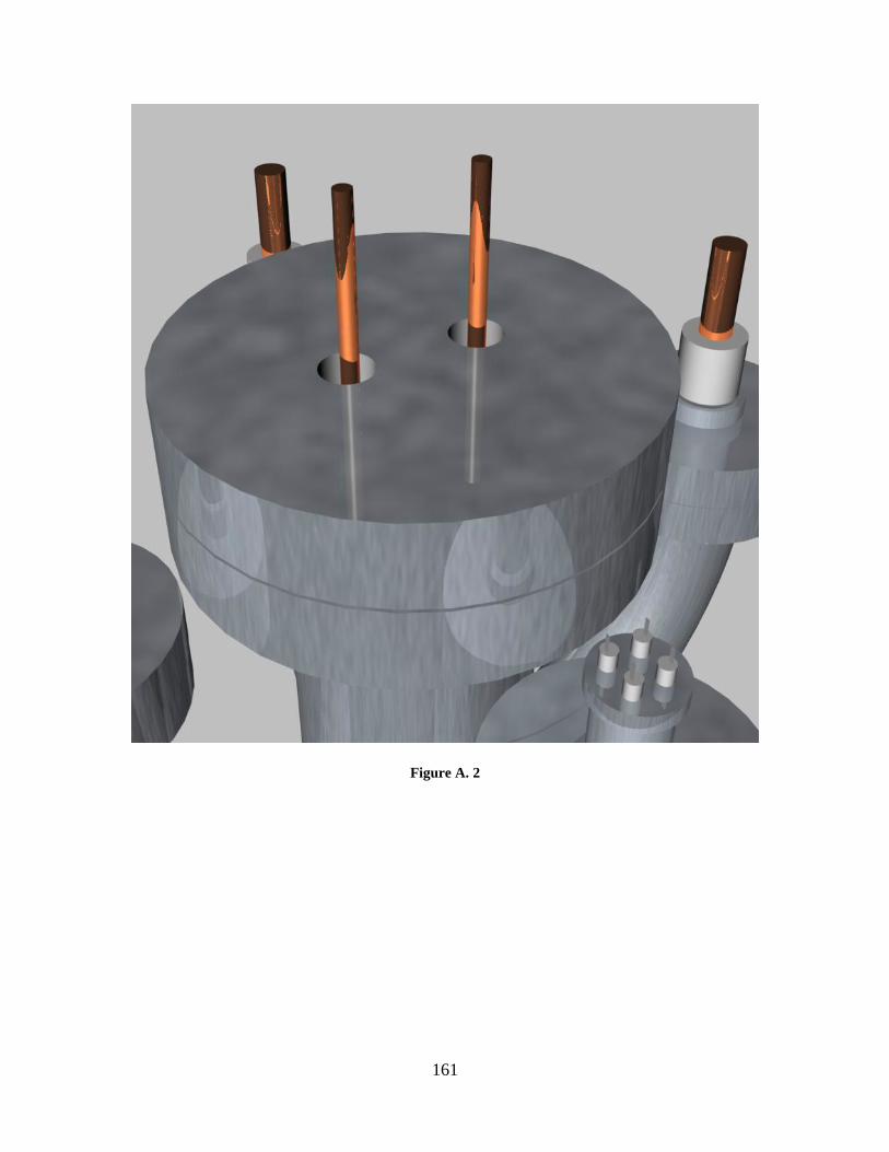
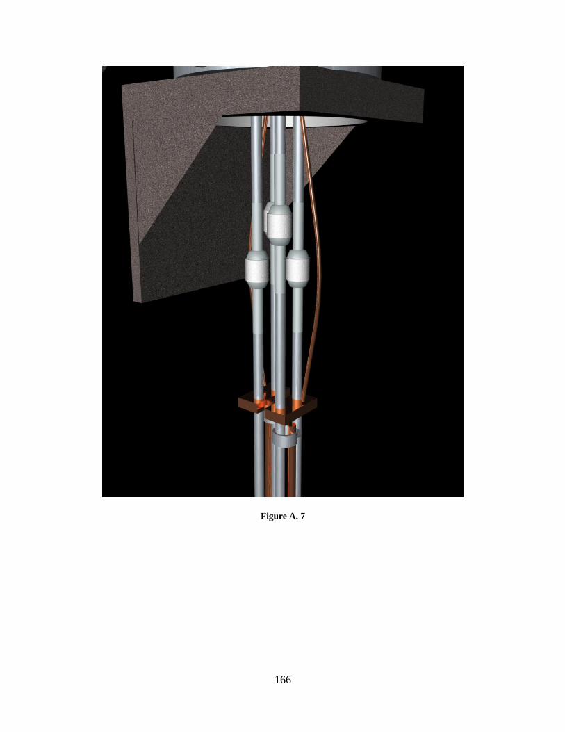
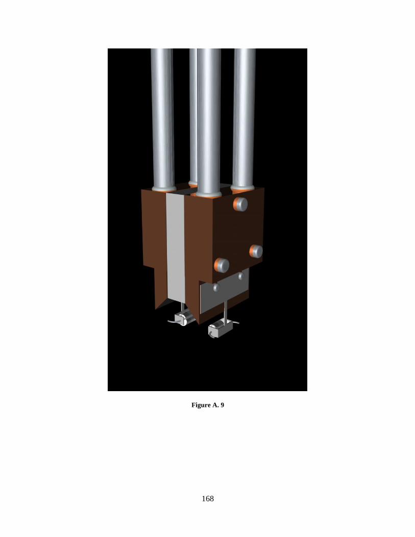
APPENDIX A: FLOW-THROUGH COOLING FOR UHV DIPSTICK ................................ 154
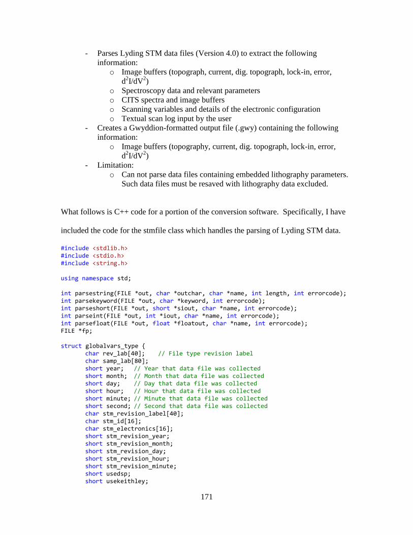
APPENDIX B: LYDING TO GWYDDION FILE CONVERSION SOFTWARE ................. 170
Page 9
1
CHAPTER 1
INTRODUCTION
1.1 Motivation
Since its mainstream introduction,1 graphene has become the focus of an
extensive collection of experimental and theoretical studies. The benefits of graphene are
many2–4
and the limitations few, but one fundamental property which limits the
widespread introduction of graphene electronic devices is the absence of an electronic
band gap. Among the solutions offered to this problem are quantum-confined graphene
ribbons,5 Bernal stacked bilayer graphene,
6 and aligned graphene films on lattice-
matched insulating substrates, such as boron nitride.7 However, each of these techniques
brings its own array of limitations and experimental challenges, and none have
established dominance in the field. Another option is the introduction of a band gap in
graphenic materials by chemical functionalization. Stoichiometric hydrogenated
graphene films, termed graphane, have been both theorized8 and experimentally realized.
9
Electron-stimulated desorption of hydrogen from graphane10
could enable the fabrication
of graphene structures confined in a graphane barrier.11,12
However, the adsorption of
small hydrogen clusters on graphene is thermodynamically unfavorable,13
and it has been
suggested that many forms of graphane are inherently unstable.14
As probable evidence
of this property, experimentally realized graphane films exhibit significantly lower
resistivity than predicted.9 As a thermodynamically-favorable alternative, graphene
fluoride has garnered significant scientific interest, owing to its known stability in bulk
form,15,16
correspondingly high resistivity,17
and ability to convert semi-metallic graphene
into a wide-gap semiconductor.18
The material also benefits from decades of
Page 10
2
experimental and theoretical graphite fluoride research,19–23
owing to industrial
applications and the importance of fluorine in the synthesis of graphite intercalation
compounds. However, isolation of monolayer graphene fluoride has occurred only
recently,24
and interest in this chemical derivative of graphene has burgeoned
accordingly.25–29
Great uncertainty persists in the field, particularly as to the presence of
long-range structural order in graphene fluoride films produced by disparate synthesis
techniques,24,25
the preferred ordering of fluorine in single-sided and double-sided
configurations, and the prevalence and nature of defects upon reduction to graphene.
The scanning tunneling microscope (STM)30
has long established itself amongst
the dominant tools for surface science and structural analysis of materials. However, the
STM is heavily dependent on the application of a sharp, resilient metallic probe used to
spatially confine tunneling current during imaging.31,32
As an element of this dissertation,
we develop a modified sputter-erosion sharpening technique, field-directed sputter
sharpening (FDSS), explore the sharpening influence of FDSS in comparison to existing
sputter erosion sharpening techniques, and apply FDSS to novel probe materials,
specifically the metallic ceramic hafnium diboride. We further apply FDSS tips for high-
fidelity nanolithography of the Si(100) 2 × 1:H surface by electron-stimulated desorption.
As processing development draws nearer the limits of scaling in electronic and
mechanical systems, we are faced with an intriguing limit of precision. With the
invention of the scanning tunneling microscope and subsequent development of scanned
probe technologies,33
it has become increasingly possible to discuss the generation of
structures and devices with near-atomic precision.
Page 11
3
The remainder of this dissertation will explore fluorinated graphene films, in
single-sided and double-sided configurations. We will consider the stability of both
chemical configurations when substrate-supported under STM imaging and patterning
conditions. We study at the atomic scale the structural decomposition of monolayer
double-sided graphene fluoride on Si(100) 2 × 1:H and the chemical interaction between
graphenic flakes and pristine substrates. Through STM, scanning tunneling spectroscopy
(STS), and X-ray photoelectron spectroscopy (XPS) we elucidate the structure of one
stable form of single-sided graphene fluoride (C4F), resolve uncertainty as to the presence
of structural long-range order in planar-sheet graphene fluoride prepared with XeF2, and
make the first STS measurements of the electronic band structure of this material.
1.2 Probe Sharpening Methodology
The sharpening of conductive probes is a broad field of research, commonly
enmeshed with the study of electron beam sources for electron microscopy,34
field
emitter arrays for display applications,35
and atomic probes for scanned probe
microscopy.31
The field has increasingly flourished since the advent of the scanning
tunneling microscope,30
an application generally dependent on the detailed structure of a
scanned probe. Sharpening techniques have previously been the focus of book chapters36
and review articles.37
The techniques employed in this dissertation and the progression of
sputter sharpening technology will be detailed. When quantifying the microstructure of a
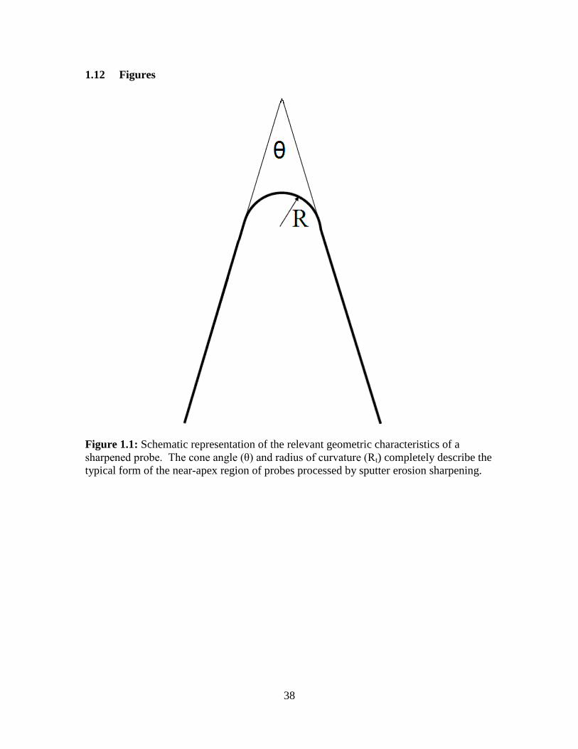
probe, a practice of measuring radius of curvature and cone angle will be adopted. As the
cone angle may vary with length scale, we take this angle to refer generally to the angle
of the smallest defined cone, proximally nearest the probe apex. A definition of these
Page 12
4
characteristics is shown schematically in Figure 1.1 (all figures at the ends of chapters).
In the literature this method of quantifying tip form is commonplace, though in some
cases the apex diameter is referenced, and defined as the width of the smallest
distinguishable apex feature.38
The term “cone angle” is frequently applied
interchangeably with the “cone half angle,” which is half of the cone angle described in
this dissertation.
1.2.1. Electrochemical Etching of Metallic Probes
Most probe materials routinely employed offer well-understood chemical or
electrochemical etch (ECE) procedures for production of sharp microtips. In one
manifestation, tungsten probes can be etched in 3M NaOH or KOH solution under an
applied DC bias, while platinum-iridium alloy can be successfully etched in CaCl2 with
an applied AC bias. Additional materials employ varied etchant and biasing conditions
and may require subsequent etch steps.39–41
In all cases, these etching procedures fall
routinely into two distinct categories, herein termed “drop-off” and “cut-off” techniques.
Under drop-off, or lamellae, etching42
the desired probe wire length is extended
through an inert counter-electrode ring within which an etchant film is confined. While
etching, this probe wire thins and breaks under applied bias, and the released wire is
captured for use. All tungsten tips reported in this dissertation were initially etched using
the drop-off technique.
Similarly, under the cut-off or emersion technique,43
several diameters of wire are
submerged in an etchant solution in the vicinity of a counter electrode. For this
dissertation, and commonly for platinum-iridium etching, this counter electrode is
Page 13
5
composed of graphite.39,44
In this configuration, a small tear-drop forms and detaches
from the wire apex, while the top probe is collected for use. In many cases, cut-off
circuitry can be employed to detect this completion event,43
while in this dissertation
some platinum-iridium probes employ a mild fine etch immediately prior to completion
to reduce etch rate significantly and allow for manual cut-off. Platinum-iridium probes
etched in-house for this dissertation were prepared using the cut-off process described
with fine etch and manual cut-off.
1.2.2. Conventional Sputter Erosion Sharpening of Metallic Probes
Since the discovery of pyramidal microstructure on ion bombarded surfaces,45
the
physics of sputter erosion have been irrevocably linked to probe sharpening, and the
ability to employ these sputter erosion techniques for the sharpening of probes has been
extensively explored.46–57
The sharpening of polycrystalline tungsten wire is widely
reported, with resulting radii of curvature between 5 nm56
and ~20 nm.54
The physics of
this sharpening technique will be described in Section 1.3.
1.2.3. Metallic Probe Sharpening by the Schiller Decapitation Process
Another intriguing technique for sharpening of metallic field emitters was
described by Schiller et al.58
and is sometimes termed the Schiller decapitation process.59
Schiller decapitation can be conceptualized as the sputter erosion analog of a cut-off
ECE, under which a metallic tip is modified by self-sputtering. With Schiller’s
technique, a negative bias is applied to a tip, inducing field ionization and subsequent
sputter erosion of the probe apex and shank. The resulting probes offer a reported radius
Page 14
6
of curvature between 4 nm and 6 nm. However, the technique requires a monitored
decapitation detection mechanism, limiting the ability of this technique to scale to highly
parallelized probe arrays. The Schiller decapitation process is the only previous example
known to the author of a field-influenced sputter erosion process, where the electric field
surrounding a biased conductive serves to direct the flux of ions. However, the technique
is differentiated from the field-directed sputter sharpening process most clearly by the
polarity of the applied bias and by the ion source itself. Where the applied negative bias
under Schiller decapitation attracts locally generated ions to the probe, under the field-
directed sputter sharpening procedure described in Chapter 2 an applied bias repels
remotely generated ions, which travel a hyperbolic path away from the probe.
1.2.4. Field-Assisted Nitrogen Reaction of Tungsten Nanotips
The process of tungsten tip etching by nitrogen in a field-directed environment
represents a related sharpening technique which is in essence the chemical analog of the
physical FDSS. One can visualize the relation between field-assisted nitrogen etching
and FDSS as that between electropolishing and sand blasting, two distinct techniques
with a shared objective. By the application of a probe bias, Rezeq et al. restrict the
reaction of nitrogen gas to the shank of a tungsten tip, thereby producing a preferential
sharpening process.60,61
The primary advantage of FDSS over this technique is the
immediate application of FDSS to multiple probe materials, including platinum-iridium
alloy and hafnium diboride, without the need to devise novel etch chemistries. In
contrast, field-assisted nitrogen etching of tungsten may produce a more chemically inert
Page 15
7
probe surface following sharpening, while FDSS probes composed of reactive materials
such as tungsten are subject to oxidation upon removal from vacuum.
1.3 Sputter Erosion Physics
Sputter-induced erosion of materials and the resulting generation of predictable
microstructured and nanostructured patterns has been a subject of research for more than
fifty years.62
Study of the stopping of particles in matter and the relation between sputter
yield and angle of incidence from which this phenomenon is derived63
dates back further
still. In his experimental result of 1959, Wehner demonstrated the sharpening of 0.5mm
diameter metallic spheres following extensive sputter erosion over hundreds of hours.62
In this early work, similar to those which followed, the spheres are electrically connected
to the grounded reference potential. The underlying physics of this sputter erosion are
well described by the Sigmund model.46
Understanding of sputter erosion physics was
additionally refined through the work of Barber et al.47
and Carter et al.50
where the
sputter erosion process is modeled with Frank’s model of chemical dissolution of crystals
by kinematic wave theory.64,65
In a straightforward model, sputter erosion of surfaces can be envisioned as a flux
of energetic ions inducing vibration and displacement of atoms within a substrate by
collision cascade.46
We can describe sputter erosion by the sputter yield:
( )
(1.1)
As expected, the sputter yield is a function of substrate material and structure, ion
species, and ion energy. Additionally, the sputter yield exhibits a curious relationship
with the angle of incidence (θ) between an ion path and the substrate, shown from
Page 16
8
theoretical modeling in Figure 1.2. When considered in terms of a cascade of atomic
collisions and a non-zero penetration depth for each ion (Figure 1.3), this result is
verified. Sputter yield is the number of displaced atoms with sufficient recoil action to
reach the sample surface and sufficient energy to overcome surface binding forces. As a
result, most sputtered atoms are surface atoms, and sputter yield is related to spatial
overlap between the sputter cascade and the substrate surface (Figure 1.4). As the angle
of incidence of an incoming ion varies from surface normal to glancing incidence, a
greater fraction of available energy is distributed in the near-surface region, increasing
the overlap between the energy distribution and surface plane, and therefore increasing
the sputter yield. An energetic ion will penetrate the surface while slowing due to the
influences of nuclear and electronic stopping. Energy from the ion is distributed within
the surface through interaction with atomic nuclei, producing an energy distribution
centered some distance beneath the surface with a distribution that is approximately
Gaussian.46
As the angle of incidence is increased, sputter yield will increase as overlap
between the sputter cascade and the substrate surface increases, thus facilitating the
escape of a larger fraction of surface atoms. Approaching glancing incidence, ion
reflection becomes increasingly prevalent. Reflection results in a rapid sputter yield
decline until erosion halts for an ion flux parallel to the surface.
In modeling conventional sputter erosion (CSE) sharpening, we consider two
distinct regimes. Under the first-order model of sputter sharpening, topographical surface
modification is considered on a scale significantly larger than the ion penetration depth.
In this case, we can model a sharpening process from the relation between yield and
angle of incidence. Modeling first-order CSE, we consider a probe of distinct, flat planes
Page 17
9
as shown in Figure 1.5. During sputter erosion, each plane will etch at a rate related to its
angle by the Y(θ) curve. As competing planes propagate, those etching most rapidly will
in time overtake more gradually etched planes, resulting in an arbitrarily sharp apex with
cone angle corresponding to the global maximum of the Y(θ) curve. Experimentally, this
maximum is found to produce cone angles of 60° – 80° for various substrate materials
and ion species.66
This first-order model provides a clear understanding of microstructure produced
by sputter erosion well beyond the nanometer scale, particularly of the probe cone angle.
However, in understanding CSE at the nanometer scale, one must more explicitly
consider the collision cascade as well as surface diffusion effects.
A second-order model of CSE follows directly from the collision cascade when
the spatial extent of this cascade is modeled. From this model, with explicit
consideration of atomic-scale effects within the cascade of influenced lattice atoms, one
can derive the effects observed under the first-order erosion model, specifically the
relation between sputter yield and angle of incidence. As described by Sigmund,51
at the
length scale of the collision cascade, sputtering of material from the target surface will
preferentially occur downstream from the impact site. Additionally, the model predicts
the formation of a depression surrounding the base of an eroded pyramid, a structural
effect verifiable experimentally in the study of sputter-induced morphological changes on
surfaces.67
Sputter erosion is reduced at the probe apex, but enhanced along the
neighboring slope, leading to a reduction of cone angle on the length scale of ion
penetration.
Page 18
10
Such collision-based erosion models do not readily explain the resulting radius of
curvature of a probe under CSE. Ultimately, the sharpening process is limited by the ion
penetration depth, and the minimum radius of curvature should be on this scale. Though
this fundamental limitation exists, those sputter erosion models described neglect the
effect of surface diffusion on the final tip shape. As explained by Carter49
and Carter et
al.50
in a first-order erosion model, the resulting probe apex is further modified by the
influence of thermally induced and radiation enhanced surface diffusion. A more
thorough derivation of sputter erosion sharpening following the work of Carter49
has been
presented previously by the author.68
This effect has been studied in detail by Bradley
and Harper53
and must be considered in the modeling of field-directed sputter erosion.
Whereas sputter erosion tends toward the general reduction of probe radius, the influence
is balanced by a preferential flux of diffusing surface atoms from the region of greatest
curvature. Such diffusion can be induced by thermal influences, localized or distributed,
or by radiation induced surface self-diffusion, described in detail by Cavaillé.69
Additionally, the effects of surface diffusion are influenced by the local electric field,70
further complicating analysis of sputter erosion sharpening.
1.4 Sputter Sharpening Apparatus
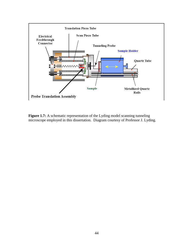
Sputter sharpening described in this dissertation was performed in the “Chamber
A” UHV system shown in Figure 1.6, located within the laboratory of Professor J.
Lyding in the Beckman Institute at the University of Illinois, Urbana-Champaign.
Sputter erosion operations were performed in a high-vacuum antechamber with a nominal
base pressure of 8 × 10⁻⁹
torr. The chamber is evacuated by a Pfeiffer-Balzers TPU-240
Page 19
11
turbomolecular pump backed by an Alcatel 2008A mechanical roughing pump. An
integrated ion source is available in the form of a Physical Electronics PHI 04-161 sputter
ion gun and corresponding OCI Vacuum Microengineering IPS3 controller. Electrical
contact to the probe is provided by dual high voltage vacuum feedthroughs which allow
for biasing and, where desirable, resistive heating. During field-directed sputter
sharpening, tip bias is applied by a Systron-Donner M107 precision DC voltage source
adjustable to 1 kV. During sputter cycling the chamber is backfilled to 5.5 × 10⁻⁵
torr of
Ar or Ne gas using a Varian variable leak valve. Chamber pressure is monitored by an in
situ nude ionization gauge and Varian Multi-Gauge controller with corresponding UHV
board (gas correction factor 1.0).
Probe characterization is performed in a Philips CM200 transmission electron
microscope (TEM) operating at 200 kV with nominal achievable resolution of 2 Å. The
CM200 includes an integrated CCD camera (2000 × 2000 pixels) for image collection.
Prior to TEM characterization, probes are removed to ambient conditions for transfer.
Additionally, the high-vacuum sputter erosion chamber is interlocked with UHV
preparation and STM chambers, both maintained below 1 × 10⁻¹⁰
torr, for which the
probes are destined. Imaging and patterning work is performed in constant-current mode
using a room temperature STM designed by Lyding et al.71
comprising two concentric
piezoelectric tubes. The inner tube provides fine probe motion and facilitates inertial
probe translation72
while the outer tube provides inertial sample translation. Microscope
control is accomplished via a digital feedback control system73
and custom software
designed by Professor Joseph Lyding et al. An STM system of similar structure is shown
schematically in Figure 1.7 and has been described previously.74
Page 20
12
1.5 Electron-Stimulated Desorption
In addition to its use for atomically resolved topographic and spectroscopic
imaging of surfaces, the local influence of the STM tips provides a high-resolution probe
for the manipulation of surfaces, a diverse array of techniques that take many forms. Such
ability was recognized from the early days of STM.75
In early demonstrations, the STM
was employed as a local probe for deposition of carbonaceous contamination,75,76
transfer
of single atoms and molecules to surfaces,77,78
and direct writing of metal nanostructures
from organometallic precursors.79
Perhaps the most memorable demonstration of this
nanomanipulative capability was the work of Eigler and Schweizer80
from which came the
iconic image of “IBM” written with 35 Xe atoms on Ni(110).
The study of electron-stimulated desorption (ESD) of atoms and molecules on
surfaces predates the invention of the STM by decades,81–84
and has been the subject of
extensive review.85,86
Like ion- and photon-stimulated desorption, ESD makes accessible
desorption processes which are unachievable by thermal effects. In general terms, ESD
proceeds by the electronic excitation of an adsorbed atom or molecule from a bonding to
an anti-bonding configuration.
It was recognized early that the STM is uniquely suited to lithographic patterning
due to the extreme spatial localization of the electron beam, leading directly to spatial
localization in the lithographic patterns produced.87
Indeed, several resist chemistries
were employed for this purpose in early studies, including carbonaceous contamination,76
calcium fluoride,88
and polydiacetylene.89
However, it was recognized that a single layer
of chemisorbed atoms offered an ideal resist layer owing to its potential for high
Page 21
13
resolution patterning and chemical contrast,90
with hydrogen as the obvious choice, given
its applicability to the technologically relevant Si surface, low atomic weight, and
compatibility with the preparation of atomically-pristine Si surfaces (unlike fluorine). An
early study of STM nanolithography was performed in air by Dagata et al.91
and
demonstrated patterned oxidation of n-Si(111):H. The patterning effect was attributed to
field-enhanced oxidation. This work was followed quickly by demonstrations of tip-
induced hydrogen desorption. Lyo and Avouris92
demonstrated induced desorption from
Si(111) following decomposition of H2O in a process then attributed to a combination of
field-induced desorption and tip-surface chemical interaction. Their work was followed by
an H desorption study from Becker et al.93
who demonstrated removal of H from the
Si(111) 1 × 1:H surface, leading to local formation of the Si(111) 2 × 1 reconstruction.
ESD lithography with a hydrogen resist was first demonstrated by Lyding et al.94
for the
purpose of patterned oxidation on the Si(100) 2 × 1:H surface. Subsequent efforts
introduced access to a vibrational heating desorption regime95
and feedback controlled
lithography (FCL), which extends to the controlled desorption of individual H atoms.96
Early patterning work has since extended to such universal processes as atomically-precise
doping of silicon,97,98
and the creation of quantum-dot cellular automata structures from
arrays of Si dangling bonds.99
These techniques provide atomic resolution patterning, and
FCL provides precise control over the number of atomic desorption events. Nevertheless,
electron-stimulated modification techniques are inherently stochastic in nature, with
patterning fidelity dependent on the spatial distribution of electron tunneling current
between tip and sample, and subject to the influence of secondary electrons.100
In the case
of ESD this effect is manifested in spurious depassivation sites distant from the pattern
Page 22
14
center. The goal of reliable and atomically-precise lithographic control of H removal by
ESD remains elusive, and becomes more important as technologically relevant patterns
approach the atomic limit.
ESD from substrates by electron transport from STM tip to sample can occur in
two distinct regimes, commonly called field emission and tunneling. Both are related and
depend on the quantum mechanical tunneling mechanism. They are distinguished by the
existence of a free electron during transmission. In the case of tunneling, the electron
tunnels directly through the vacuum gap into a substrate state, in quantum mechanical
terms never existing in the gap as a free electron. In contrast, under field emission, the
electron is field-emitted from the tip, tunneling through a vacuum gap made narrower by
the high electric field into free space before entering the substrate.
1.6 Hafnium Diboride
Hafnium diboride is one of an array of group IV diborides, and is a hard, brittle
metallic ceramic characterized by an array of advantageous mechanical and electrical
properties. In particular, in its bulk form, HfB2 has a high Young’s modulus of 504
GPa,101
high bulk hardness of 31.5 GPa,102
low room temperature electrical resistivity
between 10.6103
and 15.8 μΩ-cm,104
and a high melting point of 3240 °C.105
Various
applications for films of metal borides, and specifically hafnium diboride, have been
proposed, including wear-resistant coatings,106
resistive heating elements,107
and Cu
diffusion barriers.108
Such properties and applications, combined with the high
conductivity of HfB2 films, makes them exceptional candidates for the synthesis of ultra-
hard, chemically resistant, conductive probes for STM. The deposition process employed
Page 23
15
in this dissertation has been the subject of substantial research,109–111
and will be reviewed
here only briefly.
The synthesis of metal diborides has historically followed from high-temperature
processing above 1000 °C,112
chemical vapor deposition (CVD) from halogen-based
precursor molecules,113
or the reduction of metal oxides with boron.114
By employing the
binary tetrahydroborate hafnium borohydride (Hf(BH4)4) precursor, known to produce
non-volatile metallic borides upon decomposition,115
a low temperature CVD process is
enabled that is free of carbon and halogen contamination,116,117
with a substantial
processing temperature reduction to temperatures as low as 200 °C.108
Films deposited at low temperature (200 – 400 °C) are amorphous and of high
density.108
For deposition above 400 °C, films are crystalline but are of lower density and
possess a columnar microstructure.108,118
In other work, the annealing of amorphous films
above 700 °C was found to induce the formation of nanocrystalline HfB2 and to result in a
significant hardness increase from 20 GPa to 40 GPa.119
CVD of HfB2 from hafnium borohydride precursors opens a new avenue to the
deposition of carbon-free and halogen-free metallic films by electron beam induced
deposition (EBID).120
In particular, the probe tip of an STM has been employed for local
deposition, producing 5 nm metallic wires.121
1.7 Graphene
Scientific interest in graphene has persisted since the earliest theoretical
treatments of its unique structure and corresponding electronic characteristics.122–124
In
part, this interest arises from the importance of graphene as the fundamental building
Page 24
16
block for other carbon-based systems. Early work focused on graphene as the base unit
of graphite, and more recently graphene has garnered further attention as the structural
basis for fullerenes and carbon nanotubes.125–127
However, for decades graphene was
perceived primarily as a structure for academic treatment of other, practical
materials.128,129
It was predicted, and almost universally agreed, that such two-
dimensional materials as graphene could not exist in a stable form in isolation from bulk
support structures. In some sense, this view is warranted, and even in recent years it has
been recognized that graphene will preferentially fold, buckle, and roll itself out of two-
dimensional space given the opportunity, but the recent development of graphene
exfoliation to insulating substrates1 makes clear the limitations of this model.
1.7.1. Origins and Development of Graphene
One must note the body of experimental work that predates the mainstream
introduction of graphene to the scientific community in 2004, and the manner in which
this work has evolved to create the recent flurry of activity surrounding the study of
monolayer, bilayer, and trilayer graphene.
Among early papers on the subject, the first claim of monolayer graphene known
to the author came from the reduction of exfoliated graphite oxide in 1962.130,131
Because
the original texts are in German, we translate a relevant passage:
Page 25
17
The carbon films were obtained by the reduction of graphite oxide,
which was dispersed in dilute sodium hydroxide. From the
contrast of the electron microscope, i.e. from the electron
scattering, the thickness of these films is determined to a few
hexagonal carbon layers. The lowest values were 3 – 6 Å, and
pointed to the presence of films that consist of a single carbon
layer.131
Nevertheless, though the authors employed properly the technology and
techniques available, in light of fifty years of hindsight, the methods available
(comparison to a range of calibration standards of known thickness) introduce significant
uncertainty when attempting to characterize atomically-thin materials. Nevertheless, it is
understood that reduction of exfoliated graphite oxide is capable of producing monolayer
films,132
and therefore it may be reasonably suspected that Boehm et al. produced
monolayer graphene from graphite oxide in their work. In intervening decades, graphite
oxide films were studied extensively, and this interest has only continued to grow since
2004.132–137
The first conclusive evidence for monolayer graphene came in 1968 and 1969
when May et al.,138
based on the observations of Morgan and Somorjai,139
correctly
identified monolayer graphene in low-energy electron diffraction (LEED) patterns on the
Pt surface following exposure to various carbon precursors at temperatures from 25 °C to
1400 °C. Together with early demonstrations of few-layer graphene on Ni,140
this work
Page 26
18
represents the earliest study of graphene chemical vapor deposition (CVD) on metal
surfaces.
Since these early discoveries, graphene CVD has been reported on many
transition metal surfaces, including Pt,141–145
Ni,146–149
Pd,143
Re,150
Co,143
Ir,151–153
Ru,154–
157 and Cu.
158–161 Growth kinetics, and thus graphene thicknesses, vary by substrate
material depending on whether growth follows a precipitation162
or surface adsorption158
process. The distinction between growth processes can be clearly illustrated by isotope
labeling during growth.163
The example systems, Ni and Cu foils, demonstrate that
growth on Ni proceeds by the absorption of C into the Ni bulk at high temperature,
followed by a precipitation process during cooling. In contrast, graphene growth on Cu is
found to follow a surface adsorption process, whereby graphene islands nucleate and
grow until full surface passivation is achieved. The significance of this distinction arises
primarily in the preferentially monolayer nature of graphene grown on Cu, where on Ni
substrates growth conditions must be precisely controlled to minimize the formation of
multilayer graphene.148,149,164
CVD of graphene on Cu foil is a recent discovery158
and a
technique employed in this dissertation for the growth of monolayer graphene.
Further early work on the synthesis and etching of graphene nanostructures came
from the laboratory of Sumio Iijima, who would later be credited with the discovery of
carbon nanotubes.165
In early studies of few-layer graphene by Iijima et al.,166–168
transmission electron microscopy was employed not only to confirm the presence of few-
layer graphene but to demonstrate thinning under electron bombardment and etching by
W atoms.166
By imaging of the rolled edges of graphene flakes, films as thin as trilayer
Page 27
19
graphene could be clearly identified,166
and modified by the influence of the imaging
electron beam and deposited W adatoms.167
The graphitization of SiC upon heating was first reported by Edward Acheson and
patented in 1896 as a method for producing artificial graphite from low-quality carbon
feedstock.169
The graphitization of SiC(0001) above 800 °C (generally between 1200 °C
and 1800 °C) was well understood by the 1970s.170–172
In the decades following, the
ability to produce monolayer and bilayer graphene on the Si face of SiC was
developed,173–180
ultimately leading to the development of transfer-free graphene
electronic devices such as field-effect transistors (FETs) operating at speeds up to 100
GHz.181
By 2004 it remained unclear whether monolayer graphene existed, as it was
generally agreed to be fundamentally unstable in its two-dimensional form. Numerous
researchers worked extensively to isolate graphene by exfoliation, a process that, in
hindsight, was limited more by their ability to identify monolayers than to produce them.
It is likely that monolayer graphene is created with every pencil mark,182
but without a
mechanism to efficiently evaluate the resulting flakes, an exhaustive search becomes
overwhelmingly costly. Although thin graphite films had been produced by mechanical
exfoliation,183
the scaling of this technique to monolayer films proved difficult. This
limitation was finally overcome by Novoselov et al. in 2004,1 when they demonstrated
sufficient optical contrast in few-layer graphene to distinguish monolayer and bilayer
films. The key to this discovery was the observation of an interference effect on SiO2
films of specific thicknesses (e.g. 300 nm). As a result of this crucial discovery, the
vetting of graphene flakes produced by mechanical exfoliation (the “scotch tape”
Page 28
20
method) became practical. Ultimately, this led to the demonstration of certain physical
phenomena in graphene184,185
including the half-integer quantum Hall effect (QHE) and
Berry’s phase.
Thereafter, the study of monolayer graphene rapidly expanded to the extent that
the original 2004 paper from Novoselov and Geim has been cited between 6207 (Web of
Science) and 7477 (Google Scholar) times in the scientific literature. Between January 1,
2012 and February 28, 2012 (2:57 PM central time) 162 new research articles have been
posted to arxiv.org which contain “graphene” in their title. This phenomenon was driven
not only by the curious physics of monolayer graphene, but perhaps more so by a low
barrier to entry in a field that had been previously explored only cursorily. Suddenly
every research scientist on earth had the ability to produce monolayer graphene, literally
in their garage if they desired, and a massive body of research rushed in to the fill the
vacuum. It is beyond the scope of this discussion to review this work in its entirety,
though several books and reviews have followed the subject.2,3,186–189
We will, however, discuss recent studies of graphene growth, particularly on Cu
substrates, following the techniques employed in this dissertation for the synthesis of
single-sided graphene fluoride. As we have seen, CVD of graphene on transition metal
surfaces was one of the first techniques available for monolayer synthesis, and by 2009
similar techniques had been applied to a wide range of metals. In particular, the
formation of graphitic films on Ni was discovered as early as the 1960s,140,190
and this
substrate has remained popular due to ease of growth, low cost, and easy
transferability.164
However, given the high carbon solubility of Ni, limiting graphene
film thickness becomes a major challenge.191
Recently, Peng et al. demonstrated the
Page 29
21
reproducible, transfer-free growth of bilayer graphene on SiO2 with a Ni catalysis
layer.192
Carbon applied to the top surface of a 400 nm Ni film is absorbed during high-
temperature processing, and on cooling produces a bilayer graphene film at the Ni-SiO2
interface. Chemical etching of the Ni leaves a bilayer graphene film at the surface. Other
surfaces, such as Pt and Ir have been used to produce monolayer graphene,138,152
but high
cost and limited transferability prevent their wholesale acceptance as growth substrates.
Other researchers worked to grow graphene films directly on insulating surfaces,193
but
the quality of CVD graphene remains highest on metals.
Although in some early work, the formation of graphitic films on Cu substrates
was demonstrated as an element of diamond nucleation,194,195
it was not until 2009 that
the field began to develop rapidly due to demonstration of consistently monolayer CVD
graphene on Cu by Li et al.158
Due to Cu’s extremely low carbon solubility,196
graphene
growth on Cu proceeds by a surface adsorption process instead of bulk precipitation.163
As a result, large grains of monolayer graphene were preferentially formed under
favorable growth conditions.197
The low cost of polycrystalline Cu enables a scalable
growth process which ultimately led to demonstration of a roll-to-roll growth and transfer
process for 30 inch graphene films with Hall mobilities as high as 7350 cm2V
-1s
-1.160
1.8 Fluorinated Graphite
There has been a recent burst of interest in the chemical functionalization of
graphene films, in part as a means of improving control of its exciting, yet restrictive,
electronic band structure. As in many research fields, recent studies can draw readily on
decades of work by hundreds of early researchers. Although chemically modified
Page 30
22
monolayer graphene is a relatively new material (with the notable exception of exfoliated
graphene oxide), the chemical modification of bulk graphite has been studied extensively
over more than 60 years, and has been the focus of many published works.21–23,198,199
In
particular, fluorinated graphite has been the subject of extensive study, due in part to
industrial applications as a lubricant superior to graphite200–203
and as an excellent
cathode material for lithium ion batteries.204,205
Additionally, interest in graphite
intercalation compounds (GICs)206,199,207
directed substantial interest to fluorinated
graphite due to the intercalation of F into graphite, and its importance in the formation of
many other metal fluoride GICs.22
While countless fluoride intercalation compounds
have been synthesized and studied,19,198,20–23
for our purposes the most relevant are
planar-sheet graphite fluoride (a fluorine-graphite intercalation compound) and the
related covalent compound, puckered-sheet graphite fluoride (variously termed carbon
monofluoride, polycarbon monofluoride, or graphite fluoride). Planar and puckered
forms of graphite fluoride are the bulk lamellar analogues of single-sided and double-
sided graphene fluoride, respectively. We do not attempt a comprehensive discussion of
the wide-ranging field of fluorinated graphite, but rather introduce the bulk materials
most closely related to the monolayer films explored in this study, and highlight the most
fundamental characteristics of each.
1.8.1 Puckered-Sheet Graphite Fluoride
In its most stable form, fluorinated graphite is a covalent fluorocarbon in which the
planar aromatic backbone is converted to a puckered film of sp3 carbon. The resulting
compound generally takes the form (CF)n or (C2F)n, and in the former case has been
Page 31
23
variously termed graphite fluoride, carbon monofluoride, polycarbon fluoride,
polycarbon monofluoride, or poly(carbon monofluoride). It is the most highly
fluorinated of the various forms of fluorinated graphite, and generally exists as a gray-
white powder, or a transparent crystal in the case of highly fluorinated HOPG.208
Graphite fluoride was first synthesized by Ruff and Bretschneider15
in 1934 by the
exposure of graphite to fluorine at temperatures between 280 °C and 430 °C to produce a
fixed-valence compound of composition C1.09F. Subsequently, CxF (1.02 ≤ x ≤ 1.48) was
produced by Rüdorff and Rüdorff in 1947 between 420 °C and 500 °C.209
The original
model proposed for this compound210,211
was refined by the Rüdorff model,209
and
independently through the work of Palin and Wadsworth,212
which drew on the structure
proposed by London213
in private discussions, and was published by Bigelow214
with
acknowledgement. With a growing interest in graphite intercalation, the related planar-
sheet graphite fluorides attracted substantial interest starting in the 1970s, and will be
discussed in Section 1.8.2.
(CF)n graphite fluoride is generally believed to prefer the form of a trans-linked
cyclohexane chair,209
rather than a cis-trans-linked cyclohexane boat,215
despite early
dispute arising in part due to NMR studies indicative of a boat configuration.20
This
conclusion is also supported by the first density functional theory (DFT) study of
puckered-sheet graphene fluoride,18
wherein Charlier et al. modeled (CF)n in both boat
and chair configurations. The chair configuration was found to be energetically favorable
(0.145 eV/C-F bond), though the boat configuration was also a metastable state with a
significant (>2.7 eV) barrier for likely transition paths, suggesting that the boat
Page 32
24
configuration may be realizable, though unfavorable, depending on the kinetics of
fluorination.
Electronically, strong covalent C-F bonding in (CF)n results in an insulating gray
or white compound with a large (>3 eV) band gap. Charlier et al. report a 3.5 eV direct
band gap at the Γ point, with a 2.7 eV direct band gap at the A point.18
Interest in puckered-sheet graphite fluoride has reemerged in the last decade, due
to renewed interest in chemical functionalization of monolayer and few-layer graphene
materials. Recent experimental studies of graphene fluoride will be discussed in Section
1.9.3, but we will describe first the process and difficulties of extracting graphene from
bulk graphite fluoride.
The first experimental studies of graphene fluoride17
were enabled by mechanical
exfoliation of bulk (CF)n prepared using conventional techniques. Multilayer graphene
films were exfoliated to SiO2, with thicknesses ranging from 6 to 10 nm. Transport
measurements made on these films verified their high resistivity (~30 GΩ), a result
consistent with the large anticipated electronic band gap. Absent in this early study was
the presence of monolayer or even few-layer graphene samples. Several groups,
including researchers in the Lyding STM Laboratory, have since observed the difficulty
of exfoliating monolayer (CF)n.17,25,27,216
Although Withers et al. exfoliated monolayer
C4F, their efforts to produce monolayer (CF)n from bulk led them to describe the process
as “impossible.”27
Subsequently, Nair et al.25
did successfully demonstrate monolayer
exfoliation of 1 μm flakes, likely due to a less destructive, lower temperature fluorination
process, but described these monolayer flakes as “extremely fragile and prone to
rupture,” resorting to the on-surface fluorination of exfoliated graphene for the synthesis
Page 33
25
of larger samples. As we shall see, the work of this dissertation supports their
observation.
1.8.2 Planar-Sheet Graphite Fluoride
A related form of fluorinated graphite can be produced by the exposure of
graphite to fluorine, generally in the presence of fluoride compounds (e.g. HF, LiF, AgF).
Synthesis is often performed below 100 °C, sometimes at room temperature. In contrast
to puckered-sheet graphite fluoride, the planar form of fluorinated graphite that results
lacks the strong covalent bonding characteristic of (CF)n and (C2F)n, and is the result of
graphite intercalation by atomic fluorine. The nature of chemical bonding between C and
F varies with F concentration.217–219
For low F concentrations, roughly below C20F, C-F
bonding is ionic, and F acts as a dopant, resulting in p-doped graphite, and increasing the
electrical conductivity above that of pristine graphite.218
Conductivity increases until F
concentration reaches ~12 at%,220
above which the increasingly covalent character of C-F
bonding leads to a decrease in electrical conductivity. In the case of C4F, results vary. In
some studies, conductivity is nearly unchanged from that of bulk HOPG,220
whereas
others report a two order of magnitude decrease in conductivity when fluorinated.16
As
we shall see, this is in contrast to monolayer C4F graphene fluoride, where room-
temperature conductivity at the charge neutrality point decreases between one and six
orders of magnitude.24,27
The characteristic change from ionic to semi-covalent bonding
with increasing F concentration can also be observed in C 1s and F 1s binding energies,
measured by XPS, which increase with increasing fluorine concentration.22,218,219,221,222
These data indicate three distinct configurations of CxF, purely ionic bonding for x > 20
Page 34
26
(F 1s: ~684.5 eV, C 1s: ~284 eV), nearly ionic bonding with F locally bound to a C atom
for 4 < x < 20 (F 1s: 685.7 eV, C 1s: 284 eV), and semi-covalent bonding for x ≤ 4 (F 1s:
>685.7 eV, C 1s: >284 eV with C-F peak offset by 3.3 eV). The influence of such
variable bonding character is also seen in C-C bond length, which varies with increasing
F concentration.22
While the graphite lattice constant is 2.461 Å, a decrease of 0.24% is
seen for fluorine concentrations up to C3.5F, for which a lattice constant of 2.455 Å is
measured by X-ray diffraction.223
At higher fluorine concentrations, this lattice constant
increases to 2.478 Å for C1.3F.224
The first experimental realization of tetracarbon monofluoride was by Rüdorff
and Rüdorff in their 1947 paper.16
Planar-sheet graphene fluoride of the form CxF
(3.6 ≤ x ≤ 4.0) was formed by reaction with atomic fluorine in the presence of HF at 80
°C. It was determined that HF was necessary for the reaction to occur, and that the
fluorination process ultimately produced tetracarbon monofluoride, being unable to
proceed to the formation of CF or C2F. The product of the reaction was found to be inert
towards many acids and bases, but to decompose slowly in H2SO4 above 100 °C. Also,
Rüdorff and Rüdorff provided the first measurements of electrical resistivity in planar-
sheet graphite fluoride, finding an increase over graphite by two orders of magnitude,
from 0.02 Ω-cm in graphite to 2-4 Ω-cm in C4F. However, the resistivity of C4F was still
significantly lower than the electrically insulating (CF)n previously studied.15,209
From
their X-ray diffraction (XRD) study, Rüdorff and Rüdorff proposed the first structural
model of C4F, a model that has since been further verified and is similar to the single-
sided structure presented in this dissertation. In particular, they found that the aromatic
structure of graphite was preserved, with no indication of buckling characteristic of
Page 35
27
puckered-sheet graphite fluoride. Perhaps most importantly for this dissertation, early
XRD studies of C4F suggested the alternation of F on the top and bottom faces of each
graphene sheet, a hypothesis again proposed in recent studies of exfoliated monolayer
C4F,27
but incompatible with the single-sided fluorination presented in this dissertation.
Although discussed in a later text,19
this early work was not continued until 1970, when
Lagow et al. improved on the Rüdorff process by a static bomb synthesis technique225
during his graduate study at Rice University.198,226,215
Experimental exploration of the in-plane structure of fluorinated graphite suggests
a number of viable structures. These include the Rüdorff structure of C4F,219
the
orthorhombic system of C3.5F,227
and a hexagonal structure in C6F.228
There was a limited body of theoretical work on the electronic properties of
planar-sheet graphite fluoride before the advent of fluorinated graphene in recent years.
This was limited to preliminary results presented by Holzwarth et al. in 1983.229
Holzwarth, et al. assumed the Rüdorff model of C4F and computed a self-consistent band
structure from first principles. The results of this simulation suggested that C4F is a
semiconductor with a 2 eV band gap.
1.9 Chemically Modified Graphene
In order to enable greater control of the mechanical, thermal, and electronic
properties of graphene, various forms of graphene chemical modification have been
explored. Recent studies of graphene’s chemical derivatives follow primary on early
studies of graphite intercalation compounds (GICs)23,230,231
together with covalent forms
of functionalized graphite: graphite oxide136
and graphite fluoride.21
GICs are non-
Page 36
28
covalent lamellar structures where intercalate molecules are interspersed between sp2
bonded carbon sheets. Structures are characterized by the number of carbon layers
between intercalate layers, termed the “stage number.” For instance, a stage 1 compound
comprises alternating layers of monolayer graphene and intercalate. Stage 2 compounds
(e.g. bromine GICs) comprise bilayer graphenic films separated by intercalate.
Two distinct classes of chemically modified graphene occur in practice: covalent
and non-covalent chemistries. The most extensively studied covalent chemistries include
fluorine, hydrogen, and oxygen (in the form of graphene oxide), which produce gapped
insulators due to disruption of the graphene π-bonded network. In contrast, non-
covalently functionalized graphene generally preserves the metallic nature of graphene
but can influence various characteristics of the film including doping232
and solubility.233
1.9.1. Graphene Oxide
Graphene oxide is the earliest form of chemically modified graphene to be
discovered, and remains of profound importance today due to its increased solubility,
gapped structure, and reducibility. However, the structure of graphene oxide is non-
stoichiometric, and the reduction process results in a high density of defects. As a result,
graphene oxide has not yet been seriously considered as an electronic material. However,
recent work by Hossain et al. has indicated the possibility of a related method of
graphene functionalization, whereby oxygen is bonded in an epoxy configuration.234
Page 37
29
1.9.2. Hydrogenated Graphene
Early interest in the interaction of hydrogen with graphite and graphene235–237
centered on the development of hydrogen storage technologies,238
rather than the
electronic implications of such a structure. In graphite, hydrogen intercalation is not
generally observed, though hydrogen is incorporated into certain ternary intercalation
compounds containing alkali metals.239,240
Theoretical works have predicted a stable
hydrogenated form of monolayer graphene.8 Other studies, however, have noted a
significant nucleation barrier to hydrogenation,13
suggesting the difficulty of producing
such a material. Although hydrogenated graphene films have since been realized
experimentally,9 their stability in isolated form remains uncertain due to low resistivity,
9
and their formation appears strongly dependent upon graphene-substrate interaction.241
Although the structure of hydrogenated graphene as a trans-linked cyclohexane
chair has been predicted,8 no experimental verification of this structure is known to the
author, perhaps due to its recent discovery or to its thermodynamic unfavorability. Other
proposed single-sided structures include C2H, where H atoms bind to a single graphene
sublattice,242
and 1-D hydrogen chains separated by rippled sp2 graphene.
243
The electronic band structure of fully hydrogenated graphene was predicted
theoretically,8 and measured experimentally by angle-resolved photoelectron
spectroscopy (ARPES).244
In the same ARPES/STM study, a significant substrate
influence on hydrogen absorption was observed, where hydrogen chemisorption was
templated preferentially in the Moiré superstructure positions of the Ir(111) substrate and
graphene overlayer where graphene-substrate interaction was greatest.244
In a subsequent
study,241
the complementary influence of hydrogenation and substrate interaction was
Page 38
30
explored in detail. Covalent interaction of adsorbed hydrogen with graphene is enhanced
on highly interacting substrates, ultimately enabling a graphane-like structure with 50%
H coverage on one side, due to substrate interaction with the downward puckered C
atoms pairing with H interaction on the upward puckered C atoms. In other work by
Guisinger et al., the hydrogenation of monolayer graphene was observed by STM245
and
subsequently patterned by ESD by Sessi et al.10
Their work experimentally introduces
the theorized possibility of creating confined graphene nanostructures in hydrogenated
graphene barrier,11
but such goals have remained elusive to date.
1.9.3. Fluorinated Graphene
In direct contrast to hydrogenated graphene, and like bulk fluorinated graphite,
fluorinated graphene is thermodynamically stable and readily synthesized. Recently,
three distinct forms of graphene fluoride have been produced, which we characterized by
their fluorine concentration and atomic configuration.
The first, dilute fluorinated graphene (DFG), is characterized by an extremely
low concentration of fluorine, which serves to introduce p-type doping into the graphene
sheet. In prior studies of DFG, an unexpected colossal negative magnetoresistance effect
was seen, with a significant (×40) reduction in resistance under magnetic fields of 9 T.246
The second, ss-GF, is a covalent form of fluorinated graphene where fluorine is
confined to a single side due to the presence of some barrier to double-sided adsorption
(typically a substrate). In many ways, ss-GF is analogous to planar-sheet graphite
fluoride. For example, under typical fluorination conditions, both materials saturate in
the form of C4F, and will not readily proceed to full coverage. Additionally, ss-GF is six
Page 39
31
orders of magnitude more resistive than graphene.247
As we will show, the atomic
structure of monolayer C4F is similar to the Rüdorff structure of graphite fluoride, despite
its single-sided nature. In an early demonstration of ss-GF, Robinson et al. employ an
XACTIX XeF2 etching system similar to the one used in this dissertation to functionalize
the top side of a Cu-bound graphene sheet.247
In a different approach, Withers et al. produced graphene fluoride by the
mechanical exfoliation of planar-sheet graphite fluoride (C4F).27
While the structure of
this material approximates ss-GF, it is not strictly single-sided. Indeed, Withers et al.
suggest the alternating orientation of the Rüdorff structure, although this hypothesis
remains untested.
The third, ds-GF, or fluorographene, is a covalent form characterized by full
fluorination, CF in saturation. Ds-GF is analogous to puckered-sheet graphite fluoride,
with similarly high resistivity. Another common characteristic of ds-GF is ease of
rupture during exfoliation,25,27
possibly due to the creation of defects during the
fluorination process. In this dissertation we demonstrate ds-GF produced by mechanical
exfoliation from bulk graphite fluoride, further probing this instability by STM. In other
cases, graphene can be fluorinated on both sides after exfoliation25
or growth,247
resulting
in monolayer ds-GF. In early studies of few-layer ds-GF, Cheng et al. demonstrated
mechanical exfoliation from bulk CF.17
Subsequently, Robinson et al. demonstrated the
double-sided fluorination of CVD graphene by exposure to XeF2 on a SOI substrate, on
which Si etching facilitated the exposure of graphene’s bottom surface and creation of CF
ds-GF.247
Shortly thereafter, Nair et al. demonstrated both mechanical exfoliation of
micron-sized monolayer flakes from graphite fluoride, noting their propensity to rupture,
Page 40
32
and the fluorination of pre-exfoliated graphene by exposure to solid XeF2 at 120 °C over
days to weeks.25
Subsequently, Zbořil et al. demonstrated a liquid-phase exfoliation
process to produce monolayer ds-GF from puckered-sheet graphite fluoride.248
The goal of reducing fluorinated graphene to recover pristine graphene,
particularly in a lithographically patterned manner, has been pursued by several groups,
each with their own methods. One primary goal of ongoing study is the creation of
electronic nanostructures within fluorinated graphene films,14,249
which would enable the
production of graphene-only integrated circuits with a combination of metallic graphene
and semiconducting graphene nanowires confined within a graphene fluoride barrier. In
their earliest work, Cheng et al. reduced graphene fluoride films by annealing at 500 –
600 °C in Ar/H2 gas, a process that reduced the material and recovered a conductive
graphenic material.17
As shown later by Robinson et al. this thermal annealing process
introduces a substantial density of defects in the graphene, seen in Raman spectra. To
resolve this issue, a hydrazine treatment process250
was employed at lower temperatures
between 100 and 200 °C, resulting in efficient reduction while enabling a partial recovery
of graphene’s aromatic carbon backbone.247
Zbořil et al. contributed a chemical approach
to graphene fluoride reduction, conversion to graphene iodide by halide exchange using
KI.248
In the first demonstration of patterned reduction, Withers et al. developed an e-
beam lithographic technique for patterned reduction of C4F flakes exfoliated from bulk
planar-sheet graphene fluoride.29
Feature sizes achieved in this work were as small as 40
nm. By the inverse approach, patterned fluorination, Lee et al. created 35 nm graphene
ribbons in ss-GF.251
A polystyrene mask is applied by thermal dip-pen nanolithography
with a heated AFM tip, and a wide range of control experiments employed to verify the
Page 41
33
negligible influence of polystyrene and fluorinated polystyrene on the resulting devices.
Upon exposure to XeF2, graphene is converted to wide-gap C4F, but with the polystyrene
films acting as a mask, graphene nanoribbons are produced.
1.9.4. Chlorinated Graphene
The formation of chlorine-based GICs dates back to 1957,252
and is being studied
extensively. Although Cl2 does not intercalate into graphite253
due to poor lattice
matching with the graphite lattice,254
molecular chlorine is an important element in the
intercalation process of other species, and is cointercalated together with some materials
with which it is miscible, such as Br2255
and I2,256
thereby providing the required lattice
match. Most metal chlorides will intercalate in the presence of Cl2, and in some cases
spontaneously, where the molecule dissociates to produce Cl2.23
Unlike as for fluorine and hydrogen, it is not yet clear whether covalent
chlorinated graphene structures are experimentally realizable. In a recent study by Li et
al.,257
the existence of covalently functionalized chlorinated graphene on SiO2 was
suggested. In that work, a photochlorination procedure was employed for graphene
functionalization, wherein monolayer graphene was exposed to atomic chlorine produced
by irradiation with a Xe arc lamp. The resulting graphene exhibited covalent C-Cl
bonding with 8 at% coverage, an increase in electrical resistivity, and an increase in the
Raman D peak, indicating increased sp3 bonding character. However, these results
conflict with a subsequent study by Wu et al.258
in which graphene was exposed to
chlorine plasma, resulting in ionically bound chlorine and p-type doping, coupled with
slow etching of graphene and resulting decrease in conductivity. The disagreement
Page 42
34
between these papers was explored theoretically by Ijäs et al.259
whose simulations were
consistent with the results of Wu, et al. and suggested that the results of Li et al. could be
explained by the predicted fracturing of graphene into chlorine-terminated nanodomains.
However, the work of Ijäs et al. did not exclude the possibility of substrate-mediated
covalent functionalization of graphene by chlorine, particularly in light of earlier
observations that the substrate has a substantial influence on the covalent adsorption of
hydrogen on graphene.260,261
In fact, simulations of chlorinated graphene on various
silicon oxide surfaces suggest covalent functionalization to be achievable.259
In light of these works, we conclude that chlorinated graphene is generally
characterized by ionic C-Cl bonding, consistent with previous studies of chlorine GICs.
However, given the slow rate of etching, chlorination of graphene may offer a useful
alternative to substitutional doping for conductivity modulation. Furthermore, given an
apparent preference for covalent functionalization of graphene edges, and the instability
of adatoms bound to the graphene basal plane, Cl may have applications for edge state
passivation on graphene nanoribbons.
1.9.5. Brominated Graphene
Molecular bromine forms a GIC of stage 2 or higher,262
with a rectangular
superlattice generally of the form C7nBr2 or C8nBr2.263–266
The interlayer spacing of Br2
GICs varies from 7.03 Å for stage 2 compounds to 6.99 Å for stage 5 compounds.264
This stage 2 intercalation structure scales in a simple way from bulk graphite to
monolayer graphene, as explored by Jung et al.267
Bromine adsorbs on outer surfaces of
Page 43
35
monolayer and few-layer graphene, and intercalates into every second plane, but does not
form covalent C-Br bonds.
1.9.6. Interaction of Iodine with Graphene
It is almost universally agreed that molecular iodine does not intercalate into bulk
graphite. This result is attributed to the low electronegativity of iodine and the lattice
mismatch between molecular iodine and graphite.254
However, I2 can be cointercalated
with other halogens such as Cl2,256
and several related interhalogens form GICs.23
In the
case of monolayer and few-layer graphene, surface adsorption of I2 is observed by Jung
et al.,267
leading to p-type doping, an upward shift in the position of the Raman G peak,
and quenching of the Raman 2D peak. The doping influence of I2 is less than that of
Br2.267
Additionally, Zbořil et al. have demonstrated the chemical reduction of
fluorinated graphene by an intermediate graphene iodide phase,248
indicating both the
instability of graphene iodide and the possible application of graphene iodide chemistry
for the reduction of more stable derivatives.
1.9.7. Non-Halogen Non-Covalent Chemistries
In addition to hydrogen and halogen-based forms of CMG, numerous other non-
covalent chemistries have been explored to tune a range of graphene’s properties. These
include non-covalent functionalization for doping,232,268
nucleation promotion for
subsequent deposition steps,269
increased graphene solubility,233
lithographic
patterning,270
and band gap modulation.271
One can imagine employing a non-covalently
bound molecule as a mask for further covalent chemistries. For example, Wang and
Page 44
36
Hersam demonstrated their ability to deposit continuous monolayers of 3,4,9,10-
perylene-tetracarboxylic dianhydride (PTCDA) on the graphene surface, without regard
for defects and substrate steps.272
These films were subsequently patterned by feedback-
controlled lithography,270
and the resulting pattern employed as a mask for the deposition
of N,N′-dioctyl-3,4,9,10-perylene-tetracarboxylic diimide (PTCDI-C8) on graphene. One
can imagine a similar process by which a molecular mask is deposited, patterned, and
employed for patterned fluorination of graphene. Although PTCDA may be unsuitable
for the task, the range of adsorbates worthy of consideration is virtually limitless.
1.10 Graphene Growth and Fluorination Apparatus
Graphene studied in this dissertation was grown by CVD in the Micro and Nano
Technology Laboratory and separately in the Micro/Nanofabrication Facility of the
Frederick Seitz Materials Research Laboratory at the University of Illinois. In both
cases, growth surfaces were held in a 1 inch quartz tube and heated from room
temperature to 800 – 1000 °C by a split single-zone tube furnace. Gas delivery is
provided by means of three independent mass flow controllers which deliver Ar, CH4,
and H2. Precise growth conditions vary, and will be reported for each independent
sample.
Fluorinated graphene samples are produced by two methods. Ds-GF is produced
by mechanical exfoliation from bulk poly(carbon monofluoride) commercially available
from Acros Organics (Geel, Belgium). Ss-GF is produced by exposure of monolayer
graphene to XeF2 gas at room temperature using an XACTIX XeF2 etching system in the
Page 45
37
Micro and Nano Technology Laboratory. Fluorination times are 7 minutes and nominal
XeF2 pressure is 3 torr.
1.11 Thesis Statement
This dissertation demonstrates FDSS of tungsten, platinum-iridium alloy, and
hafnium diboride-coated tungsten, which results in a consistent improvement in scanned-
probe lithographic patterning compared with CSE and standard ECE procedures. Using
sharpened STM tips, we have identified monolayer CF flakes on the Si(100) 2 × 1:H
surface, and observed a marked fluorine instability and flake decomposition concurrent
with halogen etching of the underlying silicon substrate. In a comparison with CF, we
synthesize monolayer C4F on copper foil and characterize its structure and stability by
STM. Unlike CF, which is fluorinated on both sides, single-sided C4F is sufficiently
stable at room temperature under low-energy electron bombardment to enable atomic-
resolution imaging and the assignment of fluorine configuration by STM. We have
verified the structure of C4F by STM as well as STS, with exceptional agreement with
theoretical models of isolated, infinite C4F sheets. Furthermore, we characterize single-
and double-sided graphene fluoride by XPS, providing additional information about the
covalent C-F bonding in both forms of graphene fluoride. We conclude that fluorinated
graphene, in particular ss-GF, is a wide-gap semiconductor with potential for future
lithographic patterning and band gap modulation.
Page 46
38
1.12 Figures
Figure 1.1: Schematic representation of the relevant geometric characteristics of a
sharpened probe. The cone angle (θ) and radius of curvature (Rt) completely describe the
typical form of the near-apex region of probes processed by sputter erosion sharpening.
Page 47
39
Figure 1.2: Theoretical representation of the dependence of sputter yield on angle of
incidence. (a) Cosine dependence of energy distribution depth on angle of incidence. (b)
This relation displays a typical peak and decline resulting from the ion reflection
coefficient, R. The angular dependence of sputter yield is shown to increase for
increasing angle of incidence, before peaking at critical angle θp and falling to zero for
grazing incidence. Reprinted with permission from the Journal of Vacuum Science and
Technology B, copyright 1986, American Vacuum Society.273
a)
b)
Page 48
40
Figure 1.3: Schematic representation of sputter depth profile. Sigmund demonstrates the
influence of ion penetration depth and the distribution of the sputter cascade on sputter
erosion. The offset between the point of ion impact and the point of maximal sputter
yield is shown to result. Reprinted with permission from the Journal of Materials
Science, copyright 1973, Springer.51
Page 49
41
Figure 1.4: Schematic representation of the distribution of ion energy within the target
substrate. The arrows demonstrate path of ion approach for two distinct angles of
incidence. The distribution of ion energy is shown in green. Sputtering occurs most
frequently at points where the energy distribution and surface overlap. (a) For a steeper
angle of incidence, the overlap is less. (b) For glancing incidence, this overlap increases,
leading to an increased sputter yield.
Page 50
42
Figure 1.5: Flat-plane representation of first-order sputter erosion sharpening. Each
plane erodes at a velocity related to the sputter yield at the corresponding angle of
incidence. Ultimately, those planes which translate at maximal velocity are found to
supersede all other planes. This simple model explains the relationship between the
resulting cone angle and the relation between sputter yield and angle of incidence. The
cone angle is twice the angle corresponding to maximal sputter yield.
Page 51
43
Figure 1.6: The “Chamber A” UHV system employed in this dissertation. Indicated with
red arrows are the sputtering chamber where sputter erosion is performed (right), the
preparation chamber where sample and tip cleaning and other preparation techniques are
performed (center), and the scanning tunneling microscope (STM) chamber, where the
microscope is located (left).
Page 52
44
Figure 1.7: A schematic representation of the Lyding model scanning tunneling
microscope employed in this dissertation. Diagram courtesy of Professor J. Lyding.
Page 53
45
CHAPTER 2
FIELD-DIRECTED SPUTTER SHARPENING
In this chapter we explore FDSS, a modified sputter erosion sharpening process
capable of producing metallic tips with 1 – 5 nm radii of curvature. We will explain the
sharpening procedure in detail and demonstrate its efficacy for sharpening of platinum-
iridium alloy, polycrystalline tungsten, and diamond-like carbon (DLC). We also explore
the subject of off-axis FDSS, for cases where the ion beam is unidirectional but oriented
non-axially to the probe, and provide experimental demonstration of this effect.
We then offer a theoretical model for an ion flux in the vicinity of a biased probe,
based on the simplifying assumption of the probe tip as a perfectly conducting biased
wire in isolation, model the variation of ion flux with probe bias, and simulate the sputter
erosion process. Some of the elements of this chapter we have discussed previously by
the author.68
These results will be reviewed here, and additional data presented.
Section 2.1 will describe the FDSS process in general, and specific experimental
results will be presented in Section 2.2 for Pt-Ir alloy, and in Section 2.3 for W. We will
discuss off-axis sputtering in Section 2.4. Section 2.5 will discuss FDSS of less
conductive materials such as DLC. Section 2.6 will describe theoretical models of FDSS,
including a mathematical model of ion paths, finite element analysis of ion paths, and a
Monte Carlo simulation of sputter erosion for FDSS and CSE.
2.1. Field-Directed Sputter Sharpening
FDSS is a process related to CSE, but altered by the application of a positive
probe bias, which serves to deflect the ion beam from the probe apex in a controllable
Page 54
46
manner. A flux of inert gas ions is oriented axially along the axis of the probe wire and
tip, which has been previously sharpened to radius < 1 μm using other methods. These
energetic ions are deflected by the electric field surrounding the probe, and some
ultimately impinge upon the tip. From the point of impact, erosional processes follow the
physics described in Section 1.3 for CSE.
Two related factors influence the results of FDSS processing: modification of the
ion path and therefore angle of incidence, and a controllable and preferential reduction of
flux and surface diffusion in the apex region. We also gain the additional benefit of tip
shank shielding, where the deflected ion beam does not impact areas distant from the
apex. This shielding effect leads to a reduced etching rate and preserves any desirable
structure on the probe shank.
2.2. Sharpening of Platinum Iridium Alloy Probes
To demonstrate the FDSS process, we employ an STM tip composed of Pt-Ir
alloy (90% Pt, 10% Ir). This is a popular probe material due to its resistance to oxidation,
acceptable mechanical properties, and the high work function of Pt (5.64 eV). For our
purposes, the main advantage is oxidation resistance and the resulting ability to transfer
probes between sputtering and characterization chambers without concern for the
chemical and structural changes induced in other materials (e.g. tungsten) under ambient
conditions.
Pt-Ir probes are prepared by two techniques. Those reported here were purchased
commercially from Materials Analytical Services (MAS) Incorporated (Suwanee,
Georgia). We refer to these tips as Pt-Ir-MAS probes. In other cases, we etch probes
Page 55
47
from Pt-Ir wire39
in CaCl2 solution. We refer to these as etched Pt-Ir probes. A typical
TEM micrograph of a Pt-Ir-MAS probe is shown in Figure 2.1. Note that the typical
probe has a single apex with a radius of curvature of approximately 100 nm. There is
typically a thin layer of contamination on the probe apex, which we attribute to carbon
contamination arising from the etch process.274
On some occasions we observe
significantly thicker contaminant films, but these are easily removed by sputtering.
In one experiment, a Pt-Ir-MAS probe is characterized by TEM and then
processed by FDSS. The probe is biased at 400 V relative to vacuum chamber ground
while 2000 eV Ne ions are directed along the axis of the probe wire. Several subsequent
processing cycles are carried out under identical conditions, and the tip geometry is found
to change significantly. Initial and final TEM micrographs are shown in Figure 2.2, and
we see that the initial 100 nm tip radius is reduced to less than 1 nm. During the sputter
sharpening process, successive TEM micrographs are taken at various sharpening stages.
As seen in Figure 2.3, the tip radius progressively decreases towards equilibrium.
The final radius of curvature of the Pt-Ir probe is substantially smaller than those
previously reported for tips prepared by CSE and represents the sharpest known STM tip
prepared by sputter erosion.
Additionally, in comparison to later experiments discussed in this dissertation,
this experiment employed a reduced ion current density (resulting in slower sharpening)
and a lighter ion species (Ne rather than Ar). Both of these variables are expected to
further reduce the achievable radius of curvature.
Page 56
48
2.3. Sharpening of Tungsten Probes
Polycrystalline tungsten probes are commonly employed in STM due to their ease
of preparation and low cost. Tungsten probes produced by NaOH ECE can be further
sharpened with the FDSS procedure, under conditions similar to those employed for Pt-Ir
alloy. As a disadvantage, the ambient exposure required before TEM characterization
commonly results in oxidation of the probe apex prior to analysis. This difficulty is
eliminated if electron microscopy is foregone in favor of immediate transfer to UHV.
Results of STM characterization will be discussed in Chapter 4.
Several demonstrations of tungsten probe sharpening are provided in Figures 2.4
and 2.5. In each case, the probe radius is found to be significantly reduced from initial
conditions, and such a result is found to be typical for similarly prepared probes. Starting
from an initial radius between 10 nm and 100 nm, we find final tungsten probe radii to
fall to within a range of 1 – 5 nm, a substantial improvement over previous results from
the literature discussed in Chapter 1. It is believed that ambient exposure and
electrostatic discharge adversely affect these tungsten probes during transfer, resulting in
oxide growth. This growth appears predominantly at the probe apex, as expected, and
results in detectable blunting of the tip prior to characterization.
2.4. Off-Axis Sputter Erosion Sharpening
We now explore the nature of off-axis FDSS, where the ion beam is unidirectional,
but is misaligned with the axis of the probe wire. In a result consistent with CSE of
surfaces, we note that sharpening produces a similarly sized, sharp single-apex when
compared to axially aligned FDSS. However, the tip is oriented along the path of the ion
Page 57
49
flux, rather than the axis of the probe wire. Starting from a polycrystalline W tip
prepared by ECE (Figure 2.6a), we process the tip by FDSS (Vbeam = 2000 V,
Vtip = 400 V: Vr = 0.2). The resulting tip has a <5 nm radius of curvature on the primary
apex, but this apex is no longer axially oriented to the wire. This demonstration of off-
axis FDSS suggests that precise alignment of the probe wire to the ion beam is not
required for FDSS and that creation of novel tip geometries may be enabled by control of
the sputtering geometry.
2.5. Sharpening of Diamond-Like Carbon Probes
Given its dependence on a field-directed ion flux, FDSS is generally applicable only
to conductive materials. In the case of a more insulating tip, charge accumulation
resulting from bombardment by a positive charged ion species counteracts the deflective
influence of biasing. Sharpening occurs in the case of highly resistive materials, but the
result more closely approximates that of CSE, with a larger equilibrium radius of
curvature.
We have explored several materials in this dissertation, often targeting materials
with properties suggestive of a stable, long-lived STM tip. In Chapter 3 we explore HfB2
for this purpose, but in earlier work we considered a resistive coating of diamond-like
carbon (DLC), deposited by physical vapor deposition (PVD) by Richter Precision (East
Petersburg, Pennsylvania).
We first prepare a polycrystalline W tip by ECE and sharpen it by FDSS
(Vbeam = 1200 V, Vtip = 200 V: Vr = 0.167). The resulting tip has a sharp single-apex, but
oxidized significantly following ambient exposure (Figure 2.7a). This tip was spot
Page 58
50
welded to the head of a stainless steel bolt passed through a threaded hole in a Cu block.
The screw was then recessed into the Cu block for protection during shipping and
handling. After receipt, with the tip still recessed, the entire block was coated using
Richter Precision’s TitankoteTM
C11 DLC PVD coating technology. This process
produces a film with the specifications shown in Table 2.1.275
Table 2.1: Properties of PVD TitankoteTM
C11 DLC films from Richter Precision
Composition DLC (a-C:H)
Thickness (μm) 1.0 – 4.0
Micro-hardness (HV) 2000 – 3000
Coefficient of friction 0.1
Process temperature (°C) 204
After coating, the tip was shipped back to the University of Illinois for
characterization. It exhibited a single rounded apex with a ~300 nm radius of curvature
(Figure 2.7b). The original W core was clearly visible through the deposited film.
Adhesion of the continuous DLC coating to the W core was good, with a smooth surface
at the tip apex. The gaps visible on the coated tip are a result of the wire orientation
within the recess, where one side of the tip was oriented away from the PVD source.
Away from the apex, the films exhibited a columnar microstructure.
The tip was then processed by FDSS (Vbeam = 1600 V, Vtip = 400 V: Vr = 0.25),
resulting in a single apex with a 15 nm radius of curvature, significantly blunter than
conductive FDSS probes, but sharper than the initial tip and consistent with CSE (Figure
2.7c). It is important to note that this sharpening process was completed without
Page 59
51
stripping the DLC coating from the W tip. Therefore, even for insulating coatings, it is
possible to sharpen a very thin DLC film (e.g. for AFM applications).
Attempts to employ this tip for STM were limited by its low conductivity. Stable
scanning and spectroscopy were ultimately achieved; however, subsequent TEM images
clarify the origin of this stability. As shown in Figure 2.7d, the DLC probe apex
fractured during scanning, exposing the W core.
We conclude that DLC is a poor material for STM tips, due to its low conductivity.
However, the use of DLC for non-conductive AFM tips is worthy of further exploration.
Furthermore, increasing the conductivity of diamond or diamond-like materials by
doping may improve sharpening efficacy. Although FDSS is generally incompatible with
resistive materials, the benefit of sputter erosion sharpening remains, and the resulting 15
nm radius of curvature remains exceptional for the sharpening of DLC.
2.6. Simulation of Field-Directed Sputter Sharpening
Here we describe a simple model for ion deflection during FDSS and compute the
variation of apex ion current density as a function of probe bias. We model the tip apex
as an infinite, perfectly conducting cylinder, which is bombarded transversely with a
positively charged energetic ion beam while biased positively. Following the derivation
that we have described previously,68
we write the well-known equation of the electric
potential in which a singly ionized atom sits when in the vicinity of this infinite wire:
r
k
r
RqVrUrU tt )(
(2.1)
This represents a repulsive Kepler potential,276
and thanks to the study of planetary
motion (a related, attractive Kepler potential) by Johannes Kepler, we can immediately
Page 60
52
write an equation describing the motion of a singly-ionized atom passing near the wire,
which follows a hyperbolic path:
1cos1
0 eCr
(2.2)
2L
kmC (2.3)
2
221
mk
ELe (2.4)
Where m is the mass of the ion species, E is the initial ion energy (qVbeam), (r,θ) are
polar coordinates describing the position of the ion, θ0 is a constant of integration, and L
is the angular momentum given by:
mExL 20 (2.5)
Since we can assume the ion approaches from an infinite distance, r→∞ as θ→π/2,
we can determine the constant of integration:
ee
1arcsin
1arccos
20
(2.6)
From here, given initial conditions (ion energy, initial offset from the probe apex,
ion species) we can compute the path of each ion, determining when and where the probe
is impacted. In Figure 2.8 we model several typical paths for a 2 keV initial ion energy
and 1 keV probe bias (Vr = 0.5). The probe in our model has a 10 nm radius of curvature,
and we show ion offsets of 5 nm, 7 nm, 9 nm, and 12.5 nm. As expected, each ion
follows a hyperbolic path away from the probe apex.
This deterministic model then allows us to calculate the expected ion current density
at the probe apex under various sputtering conditions. We will first assume that the
Page 61
53
initial ion flux is uniformly distributed. Although the ion flux actually has a Gaussian
distribution, this assumption is reasonable because the ion beam diameter is ~2 mm and
our region of interest is ~100 nm.
To determine average ion flux across the probe tip, we need simply to determine
which range of initial positions leads to sputter erosion of the probe, and which range
leads to full deflection such that no sputtering occurs. We note that the largest initial
offset for which impact occurs will be that for which the ion impacts at a 90° glancing
angle of incidence (Figure 2.9). This condition relates to the case where the ion path is
perpendicular to the vector r, at the point where r equals the tip radius, Rt. To determine
this, we compute:
01cos
sin
0
0
eC
er (2.7)
Noting that C and e are finite and e is non-zero in the case of a repulsive potential,
the solution to this equation corresponds to the case where the sine term is zero:
(
) (2.8)
The case for which this occurs at the outer edge of a tip of radius Rt corresponds to:
( ( (
) (
)) ) ( ) (2.9)
Solving this equation, we note that the tip bias and initial ion energy enter the
equation only as the ratio, and we introduce the Vr term as follows:
rt V
E
qV (2.10)
In route to solving for x0 we combine Equations 2.2 and 2.9 to produce:
124
12
2
0
22
2
0 rttr VR
x
RV
x (2.11)
Page 62
54
This equation has a simple solution:
rt VRx 10 (2.12)
From these calculations, and an approximation of the relationship between yield and
angle of incidence, it becomes possible to explain the influence of modified angle of
incidence on sputtering. In Figure 2.10a, we show the calculated sputter yield at each
position across the tip apex for a 5 nm radius probe. The zero point corresponds to the tip
apex, and the 5 nm point corresponds to the edge of the tip. In the CSE case, as expected,
yield increases as we move away from the apex, and the angle of incidence changes
accordingly. Because the tip is modeled as an isolated wire, this yield drops to zero at 5
nm. For FDSS, a similar increase in yield is seen, but we see increased sputtering yield
along the sides of the tip and an inward shift in the point of maximal sputtering yield. As
the size of the tip decreases, the curve scales proportionally. Calculating this result
demands the approximation of the dependence on angle of incidence of the sputtering
yield. We employ a simple model which represents the basic trend, as shown in Figure
2.10b. The leading edge of the curve is a cosine relationship, and the falling tail is
accommodated by multiplying by a correction factor at shallow angles.
We compare this mathematical analysis to a finite element model of a more realistic
tip structure in two dimensions, shown in Figure 2.11a. We simulate a number of ion
paths around the tip by an iterative electric potential computation on a 2.5 Å square mesh,
with an iterative Poisson solver and the Jacobi method. Zero field-conditions are applied
at the left and right boundaries, and the electric potential is fixed to ground at the upper
edge and Vt at the lower edge. The tip is assumed to be at a uniform electric potential.
Within each square of the mesh the ion path is computed deterministically by Newtonian
Page 63
55
mechanics, and the path is computed recursively until impact with the tip occurs or the
ion leaves the system. For various values of Vr, the average ion current density is
determined by simulating ion flux and determining the range of initial positions for which
probe impact occurs. The results of these simulations are plotted in Figure 2.11b. Also
shown is the solid curve corresponding to Equation 2.12, in exceptional agreement with
the results of finite element analysis.
We further simulate the FDSS process by a Monte Carlo simulation of the sputter
erosion process similar to the work of Hartmann et al.277
Following an ion impact event,
“atoms” corresponding to pixels in the tip image are removed from the system with a
probability determined from Sigmund’s second-order sputter erosion theory,46
with
spread determined by TRIM and a “deflection” parameter inserted manually to account
for ions with a high angle of incidence. The process is calibrated to experimentally
determined sputter yields for the ion species and substrate material employed (Ar and
W).66
The sputter erosion process then proceeds, with ions injected randomly and
uniformly across the tip, and is allowed to follow the electric potential induced by the tip
bias. The electric potential surrounding the probe is recalculated iteratively following ion
impact. Though the process is inefficient, it is suitable for the small systems here studied.
The results of sputter erosion are shown in Figure 2.12. We find that the tip sputtered
under CSE (Vbeam = 1600 V, Vtip = 0: Vr = 0) has a more significant microstructure along
the shank, with ~10 nm features. In contrast, the tip processed by FDSS (Vbeam = 2000 V,
Vtip = 400 V: Vr = 0.2) has a smooth edge, with ~1 nm features. Because the simulation
does not fully account for surface diffusion, we do not consider the simulated radius of
Page 64
56
curvature of the apex to be a suitable metric, yet the distinction between sputtering
techniques is clear.
2.7. Discussion
The FDSS technique is found to produce exceptionally sharp probes and to be self-
limiting and reproducible. Of note is the relative improvement seen when compared with
the CSE technique. The radius of curvature for some probes was found to be ~1 nm,
below the 1.6 nm projected range for 1.6 keV Ar in Pt reported by TRIM, although in
general this range was expected to offer a lower bound for sharpening procedures. We
find that sharpening of less conductive materials, such as DLC, leads to blunter tips,
likely as a result of charge accumulation neutralizing the influence of probe bias.
Simulation results suggest that the improved sharpening efficacy of FDSS is due to a
combination of modulated ion path and reduced ion current density at the probe apex.
Page 65
57
2.8. Figures
Figure 2.1: Transmission electron micrograph of a typical MAS Pt-Ir probe. The radius
of curvature is approximately 100 nm and a mild surface contamination layer is visible.
Page 66
58
Figure 2.2: Sharpening of a MAS Pt-Ir probe subjected to FDSS. An ion energy of 2 keV
and probe bias of 400 V were employed for 195 minutes. (a) Initial probe form. (b) Final
probe form. Radius of curvature is reduced to ~1 nm.
a)
b)
100 nm
20 nm
Page 67
59
Figure 2.3: Comparison between subsequent erosion stages of a platinum iridium probe
subjected to FDSS. An ion energy of 2 keV and probe bias of 400 V were employed.
Time intervals between images are (from top to bottom): 75 min, 60 min, 30 min, 30 min.
Initial and final images correspond to those shown in Figure 2.2.
100 nm
Page 68
60
Figure 2.4: Demonstration of FDSS on a polycrystalline W probe. (a) Initial probe. (b)
Final probe. Ion energy of 2 keV and probe bias of 400 V were employed for 15 min.
The final probe radius of curvature is 1 – 2 nm when measured at the subsurface W layer.
Page 69
61
Figure 2.5: Further demonstration of polycrystalline tungsten sharpening. Ion energy of
2 keV was employed and a probe bias of 400 V was applied during sputtering, which
proceeded for 35 min. (a) Initial probe. (b) Probe following FDSS.
Page 70
62
Figure 2.6: Demonstration of off-axis sputter erosion sharpening of W. (a) Initial tip.
(b) The sharpened tip, following off-axis sputter erosion. The tip axis and ion flux
direction are shown, and the sharpened apex is aligned with the ion flux.
Ion flux
Tip axis
200 nm200 nm
a) b)
Page 71
63
Figure 2.7: Preparation and sharpening of a DLC STM tip. (a) W tip has been sharpened
by FDSS to a <5 nm radius of curvature. (b) This tip has been coated commercially with
a DLC film to a thickness of ~300 nm, resulting in a ~300 nm radius of curvature. (c)
This tip has been sharpened by FDSS, resulting in a ~15 nm radius of curvature DLC tip.
(d) After use in the STM, this tip was damaged.
20 nm
200 nm
500 nm
500 nm
a) b)
c) d)
Page 72
64
Figure 2.8: Simulation of several singly ionized Ar ion paths around a biased probe.
Probe bias is 1 kV with initial ion energy of 2 keV and tip bias of 1 kV (Vr = 0.5). Initial
ion positions are shown (50 Å, 70 Å, 90 Å, 125 Å).
Page 73
65
Figure 2.9: Calculated ion path for a glancing impact, as determined by Equation 2.9. In
this system, ion energy was 2 keV, and the probe was biased to 1.4 keV. The radius of
the probe was fixed at 100 Å, and singly ionized argon ions were assumed.
Page 74
66
Figure 2.10: Calculated sputter yield data. (a) Calculated sputtering yield relative to
distance from the apex of a 5 nm diameter tip for both CSE (black) and FDSS (red)
sharpening where FDSS uses 2000 eV ions with a 1000 V tip bias and CSE uses 1000 eV
ions with a grounded tip. Sputtering yield is compressed near the tip apex; with an
increase in yield across the edge of the tip. (b) Curve representing the approximated
yield versus angle relationship employed to calculate the curves in (a).
0 2 4 60
5
10
15
20
25
30
35
40
Sp
utte
rin
g Y
ield
(a
tom
s/io
n)
Position (nm)
0 20 40 60 80 100-5
0
5
10
15
20
25
30
35
40
Sputterin
g Y
ield
(ato
ms/io
n)
Angle of Incidence (Degrees)
a) b)
Page 75
67
Figure 2.11: Simulation of ion flux in FDSS. (a) Simulated ion paths resulting from
finite element analysis. Scalebar: 20 nm. (b) Variation of average ion flux at the tip apex
as a function of Vr (squares). This result agrees well with the calculation based on the
simple model of an infinite, perfectly conductive wire (solid line).
0.0 0.2 0.4 0.6 0.8 1.0
0.0
0.2
0.4
0.6
0.8
1.0
Re
lative
Io
n F
lux
Vr
rV1
b)a)
Page 76
68
Figure 2.12: Monte Carlo simulations of FDSS performed on W tips with singly ionized
Ar atoms. (a) The grounded probe (1600 eV ions) has a significant roughness of ~10 nm.
(b) The FDSS probe (2000 eV ions, 400 V tip bias) has much smaller surface roughness
of ~1 nm.
Grounded
Probe
Field-Directed
Sputtering
50 nm50 nma) b)
Page 77
69
CHAPTER 3
HAFNIUM DIBORIDE AS A PROBE MATERIAL FOR SCANNING
TUNNELING MICROSCOPY
One long-standing goal of the STM community is the fabrication of ultra-sharp,
stable, and resilient probe tips designed to provide reliable atomic resolution imaging and
patterning while resisting the detrimental influences of tip-sample interaction and
remaining structurally invariant under the influence of adsorbate transfer from the
surface. Many materials have been explored to address several of these issues. For
example, the use of Pt tips eliminates the troubles of tip oxidation during transfer
between preparation and scanning equipment. Tungsten is a common choice due to its
hardness and relative affordability. In the case of AFM, diamond tips are popular, but
diamond films sufficiently conductive for STM are difficult to fabricate.
Because different applications demand different characteristics in their probes, no
single material is the perfect choice. Because tips with tailorable electronic, chemical,
and mechanical properties are ideal, we seek a universal technique for the coating of pre-
sharpened STM tips with a range of materials, which can then be sharpened with FDSS
without the removal of the applied coating. As an example, we explore HfB2. As
discussed in Chapter 1, HfB2 can be deposited as a conformal coating onto a variety of
materials, including W. Among its attractive properties are extremely high hardness (20
GPa in the amorphous state, versus 3.4 GPa for W) and chemical stability. Perhaps most
importantly for our purposes, HfB2 has a high electrical conductivity (for a ceramic).
In Section 3.1 we will present our HfB2 deposition technique, performed in
collaboration with Dr. Navneet Kumar and Professor John Abelson of the Department of
Page 78
70
Materials Science and Engineering at the University of Illinois at Urbana-Champaign.
Then, in Section 3.2 we will present the results of coating sharpened W STM tips, and
sharpening these films by FDSS. In Section 3.3, we will present our STM results
demonstrating the successful application of HfB2 tips to microscopy and spectroscopy.
3.1. Hafnium Diboride Chemical Vapor Deposition
Deposition of hafnium diboride film is performed in a turbo pumped high-vacuum
chamber with a background pressure < 5 × 10⁻⁸
Torr. During deposition, the probe is
heated and exposed to the Hf(BH4)4 precursor. Film thickness is measured on an adjacent
silicon wafer by ellipsometry during growth and verified by transmission electron
microscopy of the STM tip. During deposition, tip temperature is nominally maintained
at 290 °C, and growth rate is approximately 2.5 Å/s. Following deposition, the film is
characterized by scanning electron microscopy (SEM) (Figure 3.1a) and energy-
dispersive X-ray spectroscopy (EDX) (Figure 3.1b).
3.2. Coating and Field-Directed Sputter Sharpening: Hafnium Diboride
The procedure for fabricating HfB2 probes has four steps. We first produce a W
tip with a 10 – 100 nm radius of curvature by ECE. With TEM, we verify that the tip
radius is within this acceptable range and has a single apex. We then sharpen this tip by
FDSS, producing a W tip with a <5 nm radius of curvature. Next, we deposit a ~100 nm
film of HfB2 on the W tip, increasing the radius of curvature to ~105 nm. We then
sharpen the HfB2 tip by FDSS, producing a tip with the properties of HfB2 and a radius of
curvature below 5 nm, without the need for fabricating HfB2 wires or ECE of bulk HfB2.
Page 79
71
The entire process flow is shown schematically in Figure 3.2a, where W is shown in
black and HfB2 in semi-transparent green.
Following deposition of a 75 nm nominal coating of HfB2, we are left with a W-
HfB2 tip with a 75 nm radius of curvature, shown in Figure 3.2b. This is consistent with
deposition atop a sharp W tip. Note that the film coats the extremely sharp probe apex
conformally. The surface of the tip has a roughness of approximately 5 – 10 nm, but as
we shall see this is reduced following FDSS.
We then sharpen the W-HfB2 tip by FDSS (Vbeam = 1200 V, Vtip = 200 V,
time = 60 min), after which the radius of curvature has been reduced to 4 nm, surface
roughness reduced to ~1 nm, and most asymmetry eliminated. The resulting tip is shown
in Figure 3.2c.
The resulting tip is extremely sharp in comparison with the deposited film, but we
also note that CSE has been used previously to produce molybdenum tips of a similar
size.38
Therefore, seeking to verify that the use of field-direction has significantly
influenced equilibrium radius of curvature, we run a control experiment intended to
compare FDSS with CSE. The tip shown in Figure 3.2c is returned to the sputtering
chamber and further processed under similar CSE conditions (Vbeam = 1000 V, Vtip = 0).
After sputtering, TEM indicates that the radius of curvature has increased to 13 nm.
Furthermore, the tip apex has become rougher, and additional asymmetry has been
introduced, as shown in Figure 3.2d.
Page 80
72
3.3. Scanning Tunneling Microscopy and Spectroscopy: Hafnium Diboride
Given that the tip is half of the STM system, during spectroscopy a tip’s density
of states can substantially convolve with the density of states of the sample. Typically,
the tip density of states is assumed to be constant, a reasonable first-order assumption in
the case of a free-electron-like metal. If a tip is resistive, any voltage drop across the tip
distorts the observed band structure of the substrate (e.g. a band gap will appear larger
than anticipated).
As we are employing a novel tip material such as HfB2, we must explore not only
the stability and lifespan of probes during microscopy, but also the stability and accuracy
of spectroscopy. To do so, a HfB2-coated W tip is sharpened by FDSS, transferred to a
UHV preparation chamber for a 600 °C degas, then transferred to a UHV-STM chamber
for imaging of the well-understood Si(100) 2 × 1:H surface.
We first note, as seen in the representative image of Figure 3.3a, that HfB2 STM
tips provide stable imaging with immediate and consistent dimer resolution. We do note
that this tip had a slight multiple tip with apex separation <1 nm, an observation
consistent with the 4 nm tip radius produced, but not seen in the case of W tips. HfB2
tips are found to provide stable scanning without any noticeable intrinsic tip changes over
several weeks, a substantial improvement over W tips, which typically experience
intrinsic changes over 60 – 300 min.
Also shown in Figure 3.3a are STS points, where STS data was collected with
HfB2 STM tips. Those marks shown in black were excluded from our data set because
they are directly above a visible surface defect, such as a dangling bond or surface
adsorbate. Those marks shown in red are included in our analysis. In Figure 3.3b we
Page 81
73
show a collection of constant-spacing STS data for this surface. Curves plotted in light
gray are the original I-V data for each point, shown together. The thick black curve
overlaid is the average of all data.
Several noteworthy observations can be made from this data. First, the electronic
structure of the surface is nearly invariant across multiple spectra points. The variation
we do observe is generally a doping effect, which leads to a shift in the Fermi level, and
can be a result of nearby adsorbates or dopant atoms, and is therefore attributed to
variations in the surface, rather than the tip. The measured band gap is invariant across
data points, and is consistent with the 1.1 eV band gap of Si when extrapolated to account
for the noise floor in constant-spacing STS.
HfB2 STM tips are also employed for the ESD of H from Si(100) 2 × 1:H. In
Chapter 4 we will discuss in detail the improvements offered by FDSS over alternate tip
preparation techniques, but here we demonstrate that HfB2 tips afford stable, high-
resolution nanolithography. The influence of desorption and its byproducts on the tip is
minimal. Figure 3.4a shows an example of a dimer-row desorption pattern in a false-
color three-dimensional rendering. Red areas correspond to passivated Si, blue to Si
dangling bonds which were present prior to pattern writing, and green to Si dangling
bonds generated by the STM tip. We see in this case that the pattern is extremely sharp,
but that several spurious depassivation sites are visible. These defects could be a result of
secondary electron emission from the surface.100
As we will explore in Chapter 4, ultra-
sharp STM tips seem to have minimal spurious depassivation, and extremely sharp
pattern profiles. The HfB2 tips shown here have a slightly greater radius of curvature (~4
Page 82
74
nm) than ultra-sharp W and Pt-Ir probes used in Chapter 4, and this may account for the
small amount of spurious depassivation.
3.4. Discussion
The most apparent conclusions that we draw from the results of this chapter are
the conformal coating of ultra-sharp STM tips by HfB2, particularly in the small-radius
apex region, the reduction in radius of curvature afforded by FDSS, and the high-
resolution and long-term stability afforded by HfB2 coated tips.
Like the diamond-like carbon (DLC) tips in Chapter 1, HfB2 films provide a
rounded single-apex tip. However, in contrast to the columnar structure of DLC, HfB2
films are smooth along the tip shank. The surface roughness observed on CVD films is
consistent with earlier studies of CVD-deposited HfB2.108
We do not explore the
influence of film thickness on conformality, although it could be the subject of future
study.
We find that FDSS affords improved sputter sharpening of HfB2 films, when
compared with the equivalent CSE process. We do note that FDSS-treated HfB2 tips are
slightly blunter than W or Pt-Ir tips, but their radius remains substantially smaller than
that of our control tip. Furthermore, it is believed that further optimization by adjustment
of FDSS parameters, temperature reduction, and global ion flux reduction may ultimately
bring the achievable radius in line with other materials.
As imaging probes, sharpened HfB2 tips prove exceptionally stable throughout
days and weeks of scanning, and provide consistent dimer-resolution imaging and
Page 83
75
lithography. STS data exhibit constant-spacing spectroscopy typical of Si(100) 2 × 1:H
and are remarkably consistent.
Perhaps most importantly, the sharpening of encapsulated probes is a
generalizable process. In principle, any conductive coating can be selected, thus enabling
us to tailor the properties of our tips to fit specific applications. In addition to having a
range of desirable chemical and mechanical properties, tailored probe materials have a
range of applications. For example, Ag and Au are favorable for tip-enhanced Raman
spectroscopy,278
while Pd is of interest due to the reversible formation of palladium
hydride.279
Some metals, such as Cu, catalytically form graphene,280
enabling the
formation of graphene-encapsulated tip structures.
Page 84
76
3.5. Figures
Figure 3.1: Deposition of HfB2 film on a W core and elemental analysis by energy-
dispersive X-ray spectroscopy (EDX). (a) SEM image of the shank of a HfB2-coated
STM tip. Scale bar: 2 μm. (b) EDX spectra from the shank of the tip. The image is
primarily composed of Hf, B, O, W. Sensitivity of the instrument to B is low, leading to
a small peak. The W signal arises from the W core. The O signal arises from both W
oxide in the core and a thin ~1 nm oxidation layer at the suface of the HfB2.
0 500 1000 1500 2000 2500
W M
Hf M
B K
Energy (eV)
O K
a) b)
Page 85
77
Figure 3.2: Demonstration of hafnium diboride tip sharpening. (a) The process of
coating and sharpening the tip is shown schematically. First, a tungsten tip is prepared by
ECE, producing a radius of curvature of 10 – 100 nm. Then, the W tip is sharpened by
FDSS to produce a radius of curvature <5 nm. The sharpened tip is coated with a
uniform film of HfB2, producing a radius of curvature approximately equal to the film
thickness. Finally, the coating is sharpened by FDSS to produce an ultra-sharp HfB2 tip.
(b) W STM tips coated with a 70 nm nominal amorphous HfB2 coating. The measured
radius of curvature is 75 nm and is approximately the sum of the 70 nm thick film and the
~5 nm oxidized W tip. Scale bar: 100 nm. (c) The same tip after FDSS sharpening, with
a 4 nm radius of curvature. Scale bar: 20 nm. (d) The results of a control experiment.
The tip shown in (c) was further sputtered with the tip bias removed and accelerating
voltage reduced to keep landing voltage constant. The resulting radius of curvature
increases to 13 nm. Scale bar: 20 nm.
a) b)
c) d)
Page 86
78
Figure 3.3: STM and STS of Si(100) 2 × 1:H. Data collected with a HfB2 coated W STM
tip. (a) Typical STM image demonstrating dimer-row resolution on the Si(100) 2 × 1-
reconstructed surface. The tip is stable, which was typical of imaging over the course of
several weeks. Crosshairs correspond to areas where spectroscopy data was taken. Black
cross hairs were excluded from analysis due to the presence of a defect in the area. Scale
bar: 10 nm. (b) Current-voltage spectroscopy data corresponding to the red crosshairs in
(a).
a) b)
-2 -1 0 1 2
0.01
0.1
1
10
100
Constant Spacing Scanning Tunneling Spectroscopy
Si(100) 2x1:H
Cu
rre
nt (p
A)
Voltage (V)
Page 87
79
Figure 3.4: Topographic images of nanolithographic patterns generated by HfB2 STM
tips on Si(100) 2 × 1:H. (a) False-color three-dimensional rendering of a dimer-row line.
A single dimer row has been depassivated, with some spurious depassivation sites
nearby. Red corresponds to passivated Si. Blue corresponds to pre-existing dangling
bonds. Green corresponds to dangling bonds generated by the HfB2 tip. (b) Original 2-D
topography of the same pattern.
a) b)
5 nm
Page 88
80
CHAPTER 4
SCANNING TUNNELING MICROSCOPY AND HIGH-FIDELITY ELECTRON-
STIMULATED DESORPTION
The ability to employ probes prepared by FDSS in the UHV-STM is of interest
for purposes of atomically-precise substrate modification. In addition to its imaging
capabilities, STM offers the potential for selective chemical structuring of the substrate
surface. In this case, electrons tunneling from tip to surface will be employed for the
selective desorption of hydrogen, generating a chemically-reactive dangling bond within
a H-based electron-beam resist. This process can be performed either as a single-electron
process in the field emission regime by directly elevating the bonding electron to an
antibonding state, or via a vibrational heating mechanism at lower electron energies.
Specifically, FDSS probes produce exceptional electron-stimulated desorption
patterns on the Si(100) 2 × 1:H surface.
4.1. High-Fidelity Patterning of the Si(100) 2 × 1:H Surface
The STM provides an excellent tool for tip characterization, although the width of
lithographic patterns written by the STM is a less direct measure of probe sharpness than
the radius of curvature measured by TEM. However, as lithography is the ultimate goal
of this experiment lithographic line widths are arguably the best possible metric. As the
spatial distribution of the electron tunneling current is dependent on probe radius,
electron-stimulated patterning offers a reasonable technique for probe apex
characterization. The quality of FDSS probes in STM can be demonstrated by high-
resolution imaging, but more importantly by high-fidelity lithographic patterning.
Page 89
81
Substrate patterning can be modeled simply by assuming a Gaussian spatial
distribution for the electron tunneling current and a single-electron desorption process. In
Figure 4.1 we show a typical tunneling current profile and desorption profile for a sample
bias of 6.5 V, tunneling current of 2 nA, line dose of 2 × 10⁻³
C/cm, 20 nm tip radius, and
Pt-Ir probe. The tunneling profile is dependent on tip radius and work function, but the
manner in which this distribution translates into a desorption profile depends further on
desorption yield and line dose. Thus, for a given tip radius, the desorption profile can be
tailored slightly to optimize registry with the atomic lattice. However, there ultimately
exists a lower limit to pattern width, at which point full desorption is no longer reliably
obtained at the center of the lithographic pattern and the line becomes incomplete.
We can employ a similar model to characterize typical lithographic lines
produced under various patterning conditions. In Figure 4.2, five lithographic lines are
written with a 2 nA tunneling current and 2 × 10⁻³
C/cm line dose, using an etched Pt-Ir
tip. Sample biases vary and range from 4.5 V (lower left) to 6.5 V (upper right). To
analyze these lines, we take a cross section over the area indicated by the red box
overlaid on the image. We average over the length of the line, converting the discrete
lattice sites into continuous desorption profiles. To model this data as a desorption
probability, and assuming that the line is continuous (that is, that the center of the line is
fully depassivated), which we cannot assume here for the 4.5 V line, we isolate a single
pattern, plane fit to accommodate the tilt of the sample, and normalize the data so that the
fully depassivated peak corresponds to a desorption probability of one, while the fully
passivated periphery corresponds to a desorption probability of zero.
Page 90
82
We can then compare the patterns produced by a specific STM tip to those
predicted for given patterning conditions to extract an effective tip radius. In Figure 4.3,
we show desorption probabilities for both the 6.5 V and 6.0 V lines from the patterns
shown previously. The tip radius that best fits the data is 20 nm.
In order to optimize our patterning procedure, W tips are processed by FDSS,
producing sub-5 nm radius probes. These tips can then afford ultra-high resolution
lithographic patterning, as shown in Figure 4.4. Here we demonstrate the smallest pitch
reliably achieved by FDSS probes. In this case, two dimer rows (each two atoms wide)
are patterned with a single two-atom wide dimer row between them. The grayscale 2-D
topographic image is shown in Figure 4.4b, and a false-colored 3-D rendering of the
image is shown in Figure 4.4a. The coloration identifies the surface’s patterning state.
Red areas correspond to H-passivated Si. Blue corresponds to Si dangling bonds or
adatoms that were present prior to the patterning operation. Green corresponds to Si
dangling bonds that were generated by the patterning operation. There are few
imperfections in this pattern, although four spurious dangling bonds run along the edge of
the rightmost line. These dangling bonds may be a result of imperfect tip registry with
the substrate, rather than the spatial distribution of the tunneling current. A similar
process is employed in Figure 4.5 to produce a 2-D lithographic box of reactive Si
dangling bonds. In both cases, patterning conditions included a sample bias of +4 V, a
tunneling current of 2 nA, and a line dose of 2 × 10⁻³
C/cm. Imaging was performed with
a sample bias of −2 V and tunneling current of 50 pA.
Page 91
83
4.2. Influence of Field-Directed Sputter Sharpening on Patterning
In order to verify that FDSS has a significant influence on the patterning
capabilities of W probes, we perform a series of experiments intended to compare the
same tips following a three-step preparation process: etching, FDSS, and CSE as a
control. The lines patterned after FDSS consistently have higher resolution than those
patterned by etched and control probes.
In this experiment, a single polycrystalline W probe is sequentially sharpened by
all three methods; and following each method, the probe is used for ESD of hydrogen
from a Si(100) 2 × 1:H surface. When the tip is sharpened by etching, the initial apex
(Figure 4.6a) has a 5 ±1 nm radius of curvature (11.5 ±0.5 nm oxide radius). The probe
is then degassed above 400 °C for 8 hours in UHV and used repeatedly to write a series
of lithographic lines (Figure 4.6b). The tip is then removed from the STM and sharpened
by FDSS. From a TEM micrograph (Figure 4.6c) the tip radius is 2 ±1 nm (5.5 ±0.5 nm
oxide radius). After the TEM study, the tip is reinserted into our vacuum system and
resharpened by FDSS under identical conditions to remove native oxide. After the probe
is degassed above 400 °C for 8 hours, it is again used to write a series of lithographic
lines (Figure 4.6d). Imaging and patterning resolution improve markedly.
As a control, the tip is then sputtered under CSE conditions with a 1.0 keV ion
beam and a grounded probe. Inspection via TEM (Figure 4.6e) shows that the radius of
curvature has increased to 8 ±1 nm (12.0 ±0.5 nm oxide radius). The tip is further
sputtered under identical conditions to eliminate native oxide and is again degassed above
400 °C for 8 hours before additional patterns are written. Imaging resolution is reduced;
Page 92
84
tip instability is enhanced, as indicated by multiple tip changes within the image; and
pattern width increases (Figure 4.6f).
The ability to write patterns reproducibly is also markedly better for FDSS-
sharpened probes than etched probes (Figure 4.6h). This improvement largely results
from the removal of chemisorbed and physisorbed species during sputtering, but also
addresses concerns about tip instability resulting from ion-induced radiation damage.
Even in the absence of a high-temperature anneal, typical FDSS probes provide
immediate and stable dimer resolution imaging.
It is noteworthy that our ECE probe appears exceptionally sharp as judged by
TEM (above the 95th
percentile of ECE tungsten tips from our facility), making our
observation of improvement following FDSS even more significant. Hydrogen resist
patterns produced by FDSS probes have reduced line widths compared to those made by
both ECE and CSE probes. The FDSS probe generates line widths of 2.2 nm for 4.5 V
patterns and 5.8 nm for 5.5 V patterns. By comparison, the ECE probe generates 2.8 and
7.9 nm patterns, whereas the control probe generates 2.7 and 7.3 nm patterns. Thus, the
FDSS patterns exhibit a 21% (4.5 V) and 26% (5.5 V) reduction in line width over the
ECE probe and an 18% (4.5 V) and 20% (5.5 V) reduction in line width over the control
probe. This reduction in patterning width is verified to be statistically significant by a
two-tailed Welch’s t-test (α = 0.10). A comparison between FDSS and control patterns
for both 4.5 V and 5.5 V patterns is presented in Figure 4.6g, and further data are
provided in Figure 4.7. Comparing ECE and CSE probes, we cannot reject the null
hypothesis for 4.5 V (p = 0.50) or 5.5 V (p = 0.65) sample bias, allowing for the
possibility that CSE offers no improvement over a sharp ECE probe.
Page 93
85
In a subsequent experiment, we verify the reproducibility of these results across
multiple STM tips, and across multiple tip sputtering cycles. A set of three ECE probes,
with a range of apex radii, are selected by TEM (micrographs are shown in Figure 4.8) as
clean and potentially stable STM tips. The tips are sharpened and patterns written using
the process described above and sample biases from 4 V to 8 V. Each tip was sharpened
by FDSS (Vbeam = 1400 V, Vtip = 400 V: Vr = 0.286) and, after patterning, sputtered under
CSE conditions (Vbeam = 1000 V, Vtip = 0: Vr = 0). Tip C received damage unrelated to
sputtering and scanning before the control experiment, but ECE and FDSS data are
shown for completeness. Tip A was FDSS sharpened a second time after CSE patterning,
and a second control experiment completed. The resulting pattern widths are shown in
Figure 4.9, where we see a clear and reproducible reduction in pattern width as we move
from ECE tips to CSE tips and finally to FDSS tips, for which optimal resolution is
achieved. It is noteworthy not only that each tip exhibits improved patterning after
FDSS, but that the images collected after FDSS achieve atomic resolution patterning
from the very first scan (Figure 4.10). Furthermore, the cycling of tip A through multiple
FDSS and control cycles further demonstrates the reproducibility of FDSS not only from
one tip to the next, but also for a single tip over multiple sputtering cycles.
4.3. Probe Regeneration by Field-Directed Sputter Sharpening
While operating within the STM, probes commonly undergo structural changes
due, for example, to surface diffusion or mechanical contact with the substrate being
analyzed. Though the result of a “tip change” can be advantageous, for instance, by the
creation of an atomically sharp point, more frequently imaging resolution suffers. Often
Page 94
86
changes are reversible, though the recovery process is rarely deterministic and commonly
involves aggressive tip-surface interaction until further structural modification occurs.
Unfortunately, scanned probes remain a consumable item. However, for mildly
damaged probes, regeneration by FDSS is possible. In this experiment, a polycrystalline
tungsten probe was employed in the STM for imaging and patterning of the silicon
surface. Following extended scanning, the probe sustained damage and was unable to
provide precise patterning. Figure 4.11a includes a representative pattern produced by
the degraded probe. Though evidence of atomic-scale surface structure can be discerned,
the electron-stimulated desorption patterns are broadened. Additionally, the probe
appears to have multiple apices, each of which provides an STM image of the surface in
parallel. As a result, multiple shadow images are visible on the surface for each line. It
was believed that the damaged probe used to generate Figure 4.11a would be a good
candidate for regeneration via FDSS. Without removal from high vacuum, the probe was
subjected to FDSS processing with ion energies of 1.2 keV and a probe bias of 200 V.
The probe was not imaged by TEM, but immediately degassed and returned to UHV for
further use in the STM.
The regenerated tip enabled stable imaging of the silicon surface, and high-
fidelity patterning by electron-stimulated desorption. One representative pattern is shown
in Figure 4.11b. Of particular interest is the extreme patterning precision visible in this
image. Outside of the immediate patterns, which follow the atomic dimers of the surface,
most dangling bonds are randomly distributed and created by imperfect sample
preparation, instead of electron-stimulated desorption.
Page 95
87
4.4. Discussion
In conclusion, the radius of probes has a marked effect on the width of patterns
they produce. We show that the desorption profile is a reasonable metric for the
sharpness of a tip. We then show that, under identical patterning conditions, tips
prepared by FDSS produce significantly smaller patterns than those produced by ECE or
CSE. We also show that FDSS tips produce more consistent and reproducible patterns
than etched tips, and that FDSS tips typically provide stable imaging from the first scan.
We also show that the improved patterning capabilities of FDSS-processed tips
are reproducible across multiple tips and multiple FDSS/CSE cycles for the same tip.
Finally, we demonstrate that FDSS enables the regeneration of damaged tips following
STM. Although this process is not a panacea, moderately damaged tips will benefit from
subsequent FDSS treatment and can be used and reused numerous times over extended
periods of time (sometimes months).
In conclusion, FDSS is a remarkable technique for the improvement of
lithographic patterning, which provides consistent and reproducible patterning across
multiple tips and moves towards the limit of atomically-registered and atomically-precise
lithography.
Page 96
88
4.5. Figures
Figure 4.1: Simulated tunneling current profile (black) compared to the resulting
desorption probability (blue).
Cu
rre
nt
De
ns
ity (
ele
ctr
on
s/Å
2)
Des
orp
tion
Pro
ba
bility
x (Å)
Page 97
89
Figure 4.2: Experimental extraction of desorption probability for a variety of
lithographic patterns with sample biases. (a) Topographic STM image with patterns
written from 4.5 V (lower left) to 6.5 V (upper right). (b) Topographic height is averaged
along the length of each line within the red box in (a), producing the topographic contour
shown. This data is related to the desorption probability.
25 nma) b)
Page 98
90
Figure 4.3: Comparison of experimental desorption probability with our model. After
normalization, experimental topographic contours are compared to models, and an
effective tip radius is extracted. In this case, the tip radius is 20 nm. (a) Topographic
image of all lithographic patterns. (b) Desorption probability extracted from 6.5 V pattern
(blue) compared to predicted pattern (black). (c) Desorption probability extracted from 6
V pattern (blue) compared to predicted pattern (black).
25 nm
6V
6.5V
a)
b)
c)
Page 99
91
Figure 4.4: A demonstration of atomic-fidelity lithography by electron-stimulated
desorption (ESD) of hydrogen from the Si(100) 2 × 1:H surface with a 4 V sample bias, 2
nA current setpoint, 2 × 10⁻³
C/cm line dose and FDSS-generated tungsten probe. STM
images are collected with a sample bias of −2 V and a current setpoint of 50 pA. All
scale bars are 4 nm. (a) Dimer-row line width lithography is demonstrated. The image is
a false-color three-dimensional rendering where red represents passivated silicon, blue
represents background surface features unrelated to patterning, and green represents
dangling bonds generated by the ESD process. (b) The same pattern shown in its original
form as a two-dimensional STM topograph.
a) b)
4 nm
Page 100
92
Figure 4.5: (a) A nanolithographic box 20 × 13 atoms in dimension is shown as a false-
color three-dimensional rendering similar to that in Figure 4.4a. The feature has been
generated by five successive depassivation patterns under identical patterning conditions.
(b) Topographic STM data in two dimensions for the nanobox pattern.
a) b)
3 nm
Page 101
93
Figure 4.6: The effects of probe sharpening on patterning capabilities. Each hydrogen-
resist pattern includes a sequence of lines corresponding to sample biases from lower left
to upper right of 4 V, 4.5V, 5 V, 5.5 V, 6 V, and 6.5 V with constant tunneling current of
2 nA and line dose of 2 × 10⁻³
C/cm. STM images are collected with a sample bias of −2
V and a current set point of 50 pA. All scale bars are 30 nm. (a) Transmission electron
micrograph of an exceptionally sharp tungsten probe produced by ECE. (b) A
representative pattern on the Si(100) 2 × 1:H surface written by ESD of H using the
ECE probe of (a). (c) Transmission electron micrograph of the probe following an FDSS
sharpening procedure (1.4 keV ion energy, Vr = 0.286, 38 minutes). (d) A representative
pattern created with this FDSS-generated probe. (e) Transmission electron micrograph of
the same probe following control experiment sputtering (1.0 keV ion energy, Vr = 0, 60
minutes). (f) A representative pattern created with the control probe. (g) Spatial
distribution of desorption probability for FDSS and control probe patterns at 5.5 V and
4.5 V sample bias. (h) Pattern stability achieved with an FDSS probe is compared to that
of an etched probe. All 5.5 V patterns generated by a probe before and after FDSS are
shown.
5.5 V
4.5 V
0 25 50 75 1000.0
0.5
1.0
Deso
rpti
on
Pro
bab
ilit
y
Position (Å)
FDSS
Control
a) b)
c) d)
e) f)
g)
h)
0 25 50 75 100 125 150 175
0.0
0.5
1.0
De
so
rpti
on
Pro
ba
bil
ity
Position (Å)
Etched
FDSS
5.5 V Pattern
Page 102
94
Figure 4.7: Further data from desorption patterns created by etched, FDSS, and control
probes. (a) Averaged data from each series of patterns created at 5.5 V sample bias. The
variation of widths is visible between FDSS and control cases, and also between FDSS
and etched cases, though much of this variation results from a shoulder produced by the
probe instability shown in Figure 4.6h. However, the distinction between FDSS and
etched probes becomes clearer for 4.5 V sample bias where the effects of any secondary
apices in the etched probe are dramatically reduced. (b) Averaged data from each series
of patterns created at 4.5 V sample bias. Here a clear distinction is drawn between FDSS
and etched probes, and between FDSS and control probes.
0 25 50 75 100 125 150 175
0.0
0.5
1.0
De
so
rpti
on
Pro
ba
bil
ity
Position (Å)
ECE
FDSSa)
b) c)
5.5 V Pattern
5.5 V Pattern 5.5 V Pattern
ECE
ECE ECE
FDSS
FDSS FDSSCSE CSE
a) b)
Page 103
95
Figure 4.8: Initial TEM micrographs of the tips used to generate Figure 4.9. (a) Initial
form of tip A. (b) Initial form of tip B. (c) Initial form of tip C. Scale bars: 50 nm.
a) b) c)
Page 104
96
Figure 4.9: Further patterning results from multiple STM tips. Each curve corresponds
to a set of patterns written at sample biases between 5 V and 8 V. Blue curves
correspond to ECE tips, red to CSE tips, and green to FDSS tips. FDSS clearly produces
narrower patterns, and this is most clearly visible at high sample biases.
5 6 7 80
50
100
150
200
250
Wid
th (
Å)
Voltage (V)
A Etch
B Etch
C Etch
A Control1
A Control2
B Control
A FDSS1
A FDSS2
B FDSS
C FDSS
Page 105
97
Figure 4.10: Initial imaging and patterning resolution from each of four FDSS cycles and
three FDSS-processed probes. In each case the first pattern written is shown, which
corresponds to the second image collected. Thermal drift was allowed to subside after
the sample was loaded into the STM, but no additional tip treatments were employed to
achieve this resolution. In one case (c), the tip likely acquired an adsorbate during
imaging, resulting in a slight multiple tip in the top half of this image. This adsorbate
became desorbed naturally in the course of the subsequent scan, the tip returned to its
initial state, and no lasting effect was observed on the tip’s imaging and patterning
capabilities, as shown in Figure 4.9. Scale bars: 30 nm
A FDSS 2
b)
C FDSS
c)
A FDSS 1
a)
B FDSS
d)
Page 106
98
Figure 4.11: Regeneration of damaged STM tips by FDSS. (a) Pattern resulting from
ESD of hydrogen from the Si(100) 2 × 1:H surface using a patterning voltage of +4 V
and set point current of 2 nA. The STM image was collected with a sample bias of −2 V
and a current set point of 50 pA. Scale bar: 30 nm. (b) Equivalent pattern generated by
the same probe following FDSS (Vbeam = 1.2 kV, Vt = 200 V: Vr = 0.167). Patterns were
written with a sample bias of +4 V and a current set point of 2 nA. The STM image was
taken with a sample bias of −2 V and a current set point of 50 pA. The round pattern
visible in the lower left corner was produced by the extended presence of the STM tip at
elevated sample bias. Scale bar: 20 nm.
a) b)
Page 107
99
CHAPTER 5
EXFOLIATION AND DECOMPOSITION OF PUCKERED-SHEET GRAPHITE
FLUORIDE
The most intuitive method for producing monolayer fluorinated graphene is also
among the most difficult. While the “scotch tape” mechanical exfoliation method has
proven extremely successful in the production of monolayer graphene from graphite,
when exfoliating from bulk graphite fluoride, the story is very different. Despite the
efforts of several groups,17,25,27
exfoliated monolayers of puckered-sheet graphite fluoride
are extremely difficult to isolate and prone to rupture. As we shall see, the results of this
dissertation further verify this fact, as monolayers produced are small and unstable,
ultimately producing fluorine.
In one application, functionalized graphene sheets must be selectively reduced by
chemical or electron-stimulated means to generate metallic or semiconducting pathways
within the basal plane.14,249
Scaling of these pathways provides continuous control of the
graphene band gap. Therefore, an improved understanding of the mechanism by which
this reduction proceeds is desirable.
In this dissertation we demonstrate tip-induced desorption of fluorine from
monolayer CF sheets on the Si(100) 2 × 1:H surface, as evidenced by variation in the
height of CF flakes and monolayer pitting of the silicon lattice induced by desorbed
fluorine. More generally, this dissertation provides the first STM study of monolayer ds-
GF, and in particular the first integration of this compound with the Si(100) surface, and
indicates that defluorination proceeds under scanning conditions that are commonly non-
destructive. These results also suggest the need to explore edge stability in (CF)n, and the
Page 108
100
importance of single-sided fluorination in order to limit the influence of fluorine on the
underlying substrate.
5.1. Characterization of Bulk Exfoliated Graphite Fluoride
Our source material is a commercially available graphite fluoride powder
produced by Acros Organics. As this material is primarily intended as a lubricant,
its defect density is expected to be very high, and grain size very small. To better
understand the nature of our bulk material, we perform TEM and diffraction
measurements, as well as X-ray photoelectron spectroscopy (XPS) of the bulk
product. For TEM, graphite fluoride powder is deposited on a Formvar-coated Cu
TEM grid from n-methylpyrrolidone (NMP). There are a few important
limitations to this process. First, on the basis of subsequent observations, we
determine that NMP affords the partial reduction of graphite fluoride. However,
this is not a major limitation for us, because the observation of long-range
structural order in partially reduced CF almost certainly implies similar order in
the fully fluorinated bulk material. Second, NMP dissolves Formvar, making this
transfer process extremely inefficient. Nevertheless, some small flakes of CF
supported on Formvar remain following transfer, enabling the completion of this
experiment. For XPS, graphite fluoride powder is pressed into a thin sheet of Au
foil and characterized in this form.
The results of transfer to TEM grids and characterization of a thin flake by
TEM and diffraction are shown in Figure 5.1. The flake in question is ~1 μm
wide, and exhibits the sixfold symmetric diffraction pattern typical of graphite or
Page 109
101
graphite fluoride, suggesting the presence of structural order in the bulk material
and saying little about the prevalence of defects therein.
To better understand the nature of this material, we explore the XPS
spectrum of the powder, which is shown in Figure 5.2. The spectrum suggests a
range of sp2 and sp
3 chemical bonding, with multiple fluorine bonding
configurations and a high density of defects. However, the prevalence of covalent
sp3 C-F bonding is clear, as expected for graphite fluoride in the puckered-sheet
configuration.
5.2. Dry Contact Transfer of Puckered-Sheet Graphite Fluoride
Knowing the difficulties involved in mechanical exfoliation of monolayer
graphene fluoride, we explore a technique made popular for the exfoliation of isolated
single-walled carbon nanotubes281,282
and graphene.283,284
In dry contact transfer (DCT),
a fiberglass applicator is impregnated with a dry source powder (e.g. nanotube bundles or
HOPG graphite). The applicator is loaded into a UHV system, degassed at appropriate
temperatures, and mechanically stamped onto the target substrate. This process leads to
the deposition of small monolayer graphene flakes ~10 nm wide, or isolated nanotubes,
onto the substrate. In this case we follow closely the technique for monolayer graphene
exfoliation, but impregnate the applicator with graphite fluoride powder. Degassing is
performed between 100 °C and 150 °C, well within the operating range of the material.
Following DCT to Si(100) 2 × 1:H, a microscopic white powder is visible on the surface
by optical microscopy, suggesting that large quantities of graphite fluoride have been
transferred, including bulk material. However, as we shall see, much of the surface
Page 110
102
contains small monolayer flakes which can be identified by STM, with a flake density of
approximately four flakes per 1 μm2. Few-layer and multilayer flakes are not observed in
this study, possible as a result of the weak interaction between planes in fluorinated
graphite.
5.3. Scanning Tunneling Microscopy: Monolayer Fluorinated Graphene
Following DCT, a survey scan of the Si surface reveals a large number of
2-D structures on the surface, which we identify as graphene fluoride. One
typical example is shown in Figure 5.3. Figure 5.3a shows a false-color 3-D
rendering of a flake, where Si is shown in red, and the CF flake is shown in green.
The original 2-D topographic image is shown in Figure 5.3b.
The fluorination of these flakes appears to be non-uniform, as indicated by
graphitic regions visible within flakes. For example, in Figure 5.4, the red arrow
indicates an area with a topographic height of ~3 Å, typical of graphene and
smaller than the 5 – 7.5 Å heights seen in CF flakes.
Following the location and characterization of 12 monolayer CF flakes,
we identify them in terms of average flake size and apparent topographic height.
We expect the average flake size to be similar to that of DCT-transferred
graphene, and the apparent topographic height to be similar to the interlayer
spacing of bulk graphite fluoride. This hypothesis is verified by measuring flake
heights by STM. A scatterplot of all flake widths and heights is shown in Figure
5.5. The average flake width is 18.7 Å with a large standard deviation of 8.4 Å,
and the average apparent flake height is 6.0 Å with a standard deviation of 1.1 Å.
Page 111
103
If we exclude the two outliers with heights near 4 Å, this average apparent height
goes to 6.4 Å with a standard deviation of 1.1 Å. The interlayer spacing of bulk
graphite fluoride is approximately 6.4 Å,17
which is in reasonable agreement with
our measurements. The high variance in flake height is important to note, and is
explained in terms of a different substrate (Si instead of CF) and partial reduction
of CF flakes. Consequently, we explore the electron-stimulated reduction of
graphene fluoride on Si(100).
5.4. Electron-Stimulated Decomposition: Monolayer Fluorinated Graphene
In order to better understand the influence of low-energy electron bombardment
on monolayer CF flakes, we perform an extended batch mode scan of a single flake. The
flake is scanned repeatedly with a sample bias of −2 V and tunneling current of 8 pA.
Following one hour of scanning, with a total electron dose of ~4000 C/cm2, the apparent
topographic height of this flake has been reduced from 6.4 Å (σ2 = 0.48 Å) to 4.0 Å (σ
2 =
0.47 Å), declining at 0.0014 Å/(C/cm2) (R
2 = 0.887). A full data set showing flake height
versus time is presented in Figure 5.6. Black squares represent apparent flake height in
each scan, with purple lines indicating the interlayer spacing of graphite and graphite
fluoride. Heights are measured by producing a histogram of the height of the flake and
the height of the Si surface. Both have approximately Gaussian distributions, and we
take the height as the difference between the means. The error bars are produced by
combining the standard deviations of each histogram. As a control, we also plot the
apparent height of a Si dangling bond (red circles) from the same image set, allowing us
Page 112
104
to verify that the observed change in flake height cannot be attributed to a change in the
STM tip or the influence of the STM control system.
This change in flake height explains the sizable variance in observed flake height
during our initial survey scan, and can likely be attributed to partial defluorination during
the scanning process. To further verify and understand this mechanism, we explore the
influence that this defluorination process has on the Si substrate.
5.5. Defluorination and Silicon Substrate Etching
We initially discovered accidentally that CF flakes are unstable on the Si
surface. In some cases, under normal scanning conditions (−2 V, 8 pA) flakes are
removed spontaneously from the surface, leaving the Si substrate behind. In other
cases the flakes are cut or otherwise manipulated on the surface, revealing
previously hidden Si atoms. Our ability to manipulate flakes provides an
opportunity to understand the influence of the flake on the Si substrate.
Although we do not have reliable control over the relocation and removal
of CF flakes, in some cases, we are able to take advantage of fortuitous
circumstances to explore CF-substrate interaction. In one case, shown in Figure
5.7, a CF flake was scanned several times; in this process the flake was offset
slightly by the STM tip to a location within the same scan area. We then
performed an extended batch mode over a period exceeding 45 minutes, during
which the flake height changed as shown in Figure 5.6. At the end of this time,
the flake was removed from the system and could not be relocated. It may have
been transferred to the STM tip, as tip resolution also changed concurrent with the
Page 113
105
transfer. While the Si substrate was initially pristine, following CF transfer and
scanning, a large number of monolayer vacancies appear in the Si substrate. We
believe that these defects are introduced by exposure to fluorine desorbed from
the lower face of the CF flake. The mechanism of fluorine etching of Si is well
understood,285–287
and the energetically favorable transfer of F atoms from
fluorocarbon nanostructures to Si(111) has been studied previously.288
From this observation of F-induced Si etching and the observed reduction
in CF flake height described previously, we conclude that defluorination of CF
occurs under mild scanning conditions (−2 V, 8 pA). We also note that flakes
often rupture during scanning, which agrees with similar observations made
during mechanical exfoliation.
5.6. Discussion
Mechanically exfoliated CF flakes are poorly suited to integration with electronic
devices, in part because of their instability, propensity to rupture, and double-sided
nature. Because fluorine is trapped between the flake and substrate, fluorine-substrate
chemical interaction is possible. We also present the first demonstration of tip-induced
defluorination of a fluorocarbon nanostructure, and specifically of monolayer graphene
fluoride. Given our ultimate goal of producing graphene structures in fluorinated
graphene films, an improved understanding of this desorption mechanism is necessary.
Ultimately, we wish to apply the knowledge gleaned from this study to single-sided
structures from which fluorine can be desorbed with neither confinement beneath
graphene nor deleterious effect on the chosen substrate.
Page 114
106
It is also noteworthy that the DCT process is applicable to exfoliation of graphite
fluoride, while traditional exfoliation cannot easily produce monolayer films. The
success of DCT is not just a testament to the universal applicability of DCT, however; it
also follows from the much smaller flake size observed in DCT-prepared samples.
Indeed, the largest flake observed by exfoliation in other work is 1 μm,25
which is much
larger that our samples but achieved much less consistently. Ultimately, DCT is a
technique applicable to surface science studies of exfoliated CF flakes on prepared
conducting or semi-conducting surfaces. Through an atomic-scale understanding of the
interaction between CF and various substrates, scalable techniques for the production of
fluorinated graphene may be discovered or enabled.
Page 115
107
5.7. Figures
Figure 5.1: TEM micrograph of CF flake on a Formvar grid. The inset shows a
diffraction pattern corresponding to this flake, with the expected sixfold symmetry typical
of graphitic material. The lattice constant cannot be conclusively determined because the
diffraction system was not fully calibrated during this experiment.
Page 116
108
Figure 5.2: XPS spectrum of the C1s peak of fluorinated graphite pressed into Au foil.
The spectrum suggests a high degree of fluorination but additionally a high defect density
and wide range of C-F bonding configuration, which is consistent with a low-quality
sample.
300 295 290 285 280
Co
unts
Binding Energy (eV)
Page 117
109
Figure 5.3: Mechanical exfoliation of monolayer CF by dry-contact transfer and
characterization by scanning tunneling microscopy (STM). (a) False color, three-
dimensional rendering of an exfoliated CF platelet. Green areas represent the CF platelet,
and red represents the underlying Si(100) surface. (b) A similarly exfoliated CF flake.
10 15 20 25 30 35 400.00.51.01.52.02.53.03.54.04.55.05.56.06.57.07.58.0
Heig
ht
(Å)
Width (nm)
a)
c) d)
b)
Page 118
110
Figure 5.4: A third, larger, flake of CF, demonstrating non-uniformity of fluorination. In
this case, a small region of the flake is graphene-like with a topographic height of ~3 Å.
The remainder of the flake is fluorinated to varying degrees. Scale bar: 10 nm.
10 15 20 25 30 35 400.00.51.01.52.02.53.03.54.04.55.05.56.06.57.07.58.0
He
igh
t (Å
)
Width (nm)
a)
c) d)
b)
Page 119
111
Figure 5.5: Scatter plot of the topographic height and maximum lateral dimension of all
CF flakes characterized by STM. Indicated in red is the interlayer spacing of CF17
for
comparison. All of the flakes observed were less than 40 nm in lateral extent. The
significant variation observed in topographic height is evidence of the observed non-
uniformity in source material fluorination, as well as electron-stimulated modification of
the platelets.
10 15 20 25 30 35 400.00.51.01.52.02.53.03.54.04.55.05.56.06.57.07.58.0
Heig
ht
(Å)
Width (nm)
a)
c) d)
b)
Page 120
112
Figure 5.6: Measured height variation of a single CF flake during scanning. Sample bias
is −3 V and tunneling current setpoint is 8 pA. Flake height falls linearly under electron
bombardment, until saturating at a topographic height of ~4 Å. Also shown as a control
is the observed height of silicon dangling bonds on the Si(100) 2 × 1:H surface, taken
from the same STM images. Unlike CF flakes, silicon dangling bonds show negligible
variations in height throughout the course of the experiment.
Graphene Fluoride
Graphene
0 2000 4000
2
4
6
0 32 64 Scan Time (min)
Flake Height
Dangling Bond Height
Fla
ke H
eig
ht
(Å)
Dose (C/cm2)
Page 121
113
Figure 5.7: Unlike graphene, CF is weakly adhered to the Si substrate. As a result, it can
be manipulated by the STM tip, including cutting, pushing, and removal from the surface.
After manipulation or removal, fluorine etching of the first atomic layer of the silicon
substrate is observed, offering further evidence for electron-stimulated defluorination of
CF films. Scale bars: 10 nm. (a) CF flake on Si(100) 2 × 1:H. This flake has undergone
extensive scanning (dose: 4000 C/cm2) and the topographic height has been reduced to
~4 Å. (b) Height contour of flake, demonstrating flake height. (c) Identical silicon
substrate after removal of CF flake by STM tip manipulation. The silicon substrate is
extensively pitted by fluorine etching. (d) Height contour of the pitted silicon substrate.
0 100 200
0
2
4
6
Hei
ght
(Å)
Distance (Å)
0 100 200
0
2
4
6
Hei
ght
(Å)
Distance (Å)
a)
b)
c)
d)
Page 122
114
CHAPTER 6
ATOMIC AND ELECTRONIC STRUCTURE OF SINGLE-SIDED GRAPHENE
FLUORIDE
Fluorinated graphite is produced in puckered and planar forms, distinct in their
synthesis and in-plane structure. Fluorination by molecular fluorine between 200 °C and
630 °C produces puckered-sheet graphite fluoride with a puckered sp3 graphitic backbone
of the form CF or C2F. In contrast, room temperature fluorination by atomic fluorine,
often produced from XeF2, produces a more planar graphite intercalation compound CxF
(x > 2) wherein the C4F in-plane structure is historically known16
and commonly
encountered experimentally.219
Similar processing has now been applied to monolayer
graphene. Although large sheets of substrate-supported monolayer ds-GF are difficult to
achieve,17,27
a form analogous to planar-sheet graphite fluoride can be synthesized by
single-sided XeF2 exposure, leading to ss-GF which saturates as C4F.247
Given
indications of C-F2 and C-F3 bonding247
and the predominance of variable-range hopping
as an electron transport mechanism,27
the presence of long-range order in ss-GF remains
a subject of dispute. Atomic-scale in-plane structure is of profound importance to the
application and control of electronic and magnetic properties. For example, atomically-
ordered C4F films have been suggested to serve as a barrier for quantum-confined
nanoribbons,14,249
yet the edge structure of graphene nanoribbons plays an important role.
Furthermore, numerous metastable configurations of fluorinated graphene are expected to
possess novel carbon-based ferromagnetic or ferrimagnetic properties289–291
of interest for
spin manipulation, but cannot yet be achieved experimentally, and depend heavily on the
precise atomic ordering of adsorbed fluorine adatoms.292
In this study, by STM, STS,
and XPS we explore for the first time the atomic-scale structural and electronic
Page 123
115
characteristics of C4F ss-GF. We produce the first atomically resolved images of
monolayer fluorinated graphene, and find it to possess a wide electronic band gap and
structural order on Cu(111) and Cu(311). We further investigate the stability of ss-GF
during thermal annealing in vacuum. We find that the underlying Cu substrate exerts a
pronounced influence on graphene fluoride, in contrast to CVD graphene films which
span defects and topographic modulation on the polycrystalline Cu surface
indiscriminately.161
Monolayer ss-GF films are produced by a two-step growth and fluorination
process. We grow monolayer graphene by CVD on polycrystalline copper foil158
at
1000 °C for 25 minutes (50 sccm H2, 850 sccm CH4). Following growth, the presence of
graphene is confirmed by Raman spectroscopy and XPS. Graphene is subsequently
fluorinated by exposure to XeF2 gas at room temperature for 7 minutes in an XACTIX
XeF2 etching system.247
The films are not removed from the Cu foil, thereby producing
the cleanest possible interface and facilitating STM of the wide-gap fluorinated graphene
film while minimizing band bending.
6.1. X-ray Photoelectron Spectroscopy and Influence of Annealing
In Figure 6.1, the composition of the resulting film is characterized by XPS, and
the effect of thermal annealing explored. We extract by XPS a C/F ratio of 5.3. This ratio
is consistent with C4F, given that approximately 70% of the Cu surface is monolayer with
a substantial bilayer component, typical for the growth conditions employed. We
identify the following chemical states293
for carbon atoms in our system: 71.7% C, 6.7%
semi-ionic C-F, 7.3% covalent C-F, 4.5% C-F2, 9.4% C-F3. The surface contains a
Page 124
116
significant fraction of C-F2 and C-F3 bonding, more than could be explained by sparse
point and line defects in CVD graphene.161
Graphene fluoride is degassed for 17 hours at
120 °C in UHV below 1 × 10⁻¹⁰
torr, and then annealed for 10 minutes between 350 °C
and 400 °C in UHV. After imaging the sample by UHV-STM, we collect further XPS
data (Figure 6.1c-d) to elucidate the influence of annealing. We measure a C/F ratio of
11.6. Identification of the chemical state of carbon in our annealed system provides the
following: 77.1% C, 5% semi-ionic C-F, 10.9% covalent C-F, 0.0% C-F2, 6.9% C-F3.
We conclude that the UHV thermal reduction process primarily induces desorption of C-
F2 and C-F3 species, preserving C-F bonded carbon. As we learn by STM, STS, and
ARPES studies, this reduction is predominantly restricted to rough Cu surfaces, while
long-range order and the wide band gap of C4F persists on well-ordered Cu(111) and
Cu(311) facets. Both before and after annealing, the binding energy of the F 1s electron
(calibrated to Cu 2p 3/2 at 932.6 eV) is 689.5 eV, substantially higher than in planar-
sheet graphene fluoride.294
This suggests a strong covalent bond and potentially non-
planar structure for ss-GF, and thus we do not adopt the “planar-sheet graphene fluoride”
nomenclature.
6.2. Scanning Tunneling Microscopy: Order in Graphene Fluoride
Following anneal, the sample is transferred to a home-built UHV-STM operated
at room temperature.71
Many facets of the polycrystalline copper surface exhibit
substantial surface roughness yet are passivated by graphene and remain pristine
following atmospheric exposure. This surface passivation effect has been observed
previously,295
and we verify the passivation of our sample by XPS spectra of the Cu 2p
Page 125
117
doublet (Figure 6.2). While it has been observed that some cold-rolled copper foils
exhibit a predominant (100) surface orientation,296
EBSD data collected on our samples
suggest a wide range of surface textures (Figure 6.3). To overcome the inherent
roughness of this surface, STM imaging is performed on (111) and (311) facets which are
identified by low-resolution batch scanning over a 25 μm2 area. Scanning is almost
universally stable, although clear atomic-resolution imaging of C4F is achieved
exclusively on atomically-flat Cu(111) (Figure 6.4). Covalent fluorine adatoms appear as
topographic protrusions in filled-states imaging under conditions selected to avoid the
wide gap of the fluorinated graphene overlayer (−4 V sample bias, 10 pA tunneling
current), so as to image C4F rather than the metal-insulator interface. Topographic
images of the system clearly indicate a hexagonal in-plane superlattice. In this
configuration, F atoms, confined to the top side of the graphene basal plane, are bonded
in a super-cell with a lattice constant twice that of graphene (Figure 6.4a-b), disrupting
transport and converting semi-metallic graphene into a wide gap semiconductor. The ~4
nm topographic modulations visible in Figure 6.4b constitute a Moiré superstructure
which we will explore in greater detail. Identical ordering of fluorine can be found on
multiple Cu(111) facets, but cannot be directly observed on high-index Cu. However, as
we will see, Cu(311) exhibits a Moiré superstructure consistent with a C4F overlayer.
STS shows a band gap on all studied facets, even high-index surfaces, although the band
gap is reduced on high-index surfaces. No other low-index Cu facets were studied, thus
we cannot rule out the possibility of a similar result on the Cu(100) or Cu(110) surface.
As a control, STM studies of pristine graphene on copper were performed and exhibit the
Page 126
118
anticipated lattice structure, as shown on an identical scale in Figure 6.4c. These images
of graphene on copper are consistent with earlier studies of the material.161
Furthermore, by STM we can verify the monolayer nature of our fluorinated
graphene films and identify conclusively the underlying Cu substrate and its orientation
relative to the ss-GF overlayer. As a near-surface imaging technique, STM is capable of
detecting the electronic influence of sub-surface atoms, in this case the Cu substrate.
This electronic interaction produces Moiré superstructure arising from lattice
misalignment between these two stacked, crystalline materials. In cases where the Moiré
pattern is hexagonal (Figure 6.5), we identify the underlying Cu substrate as Cu(111), the
only hexagonal low-index surface of Cu thus capable of producing a hexagonal Moiré
pattern with C4F. In one instance, two orthogonal surfaces were visible and identifiable
as Cu(111) and Cu(311) (Figure 6.6), and this identification allows the substrate
orientation to be precisely defined. To help rule out the possibility that the Moiré pattern
could arise from turbostratically stacked bilayer graphene, we model the system from
direct observation of the orientation of fluorinated graphene and Cu. The predicted
Moiré structures on both Cu(111) (Figure 6.6) and Cu(311) (Figure 6.7) agree with our
experimental observations, and we thus conclude that the superstructure results from
electronic interaction between C4F and Cu. As we shall see, this interaction leads also to
the visibility of the Cu(111) surface state.
We also show in greater details the superstructure visible on Cu(311). In Figure
6.8, we show a topographic image of C4F on Cu(311) with a derivative inset in the upper
left showing the transition into an adjacent Cu(111) facet where the C4F atomic structure
Page 127
119
is visible. Also shown are contour plots running across and along the “beans” of the
Moiré superstructure.
6.3. Scanning Tunneling Spectroscopy: Graphene Fluoride Band Structure
Fluorinated graphene is currently of interest for its electronic properties, and for
this reason we employ STS to extract the electronic band structure. The predicted (>3
eV) wide-gap electronic structure of fluorinated graphene is observed in all cases (Figure
6.9). Also observed is the presence of a gap state near the Fermi level, which we attribute
to the Cu(111) Shockley surface state. Focusing specifically on the well-characterized
facets described in Section 6.2, we approximate the local density of states (LDOS) of C4F
by normalized dI/dV calculated from variable-spacing STS (−2 Å).297
Our results are
consistent with theoretical predictions and reproducible between data points and distant
Cu facets.
The electronic state visible near −0.6 eV is assigned to the Cu(111) surface state,
while the state near 1.7 eV is the C4F conduction band edge.298
The observed valence
band edge of C4F is near the Cu d-band state, thus requiring further study to distinguish
the two. Comparing STS on Cu(111) and Cu(311) (Figure 6.10) we find C4F on Cu(311)
to be p-doped, an unexpected result that may follow from interaction between ss-GF and
periodic charge modulation on the Cu(311) surface.161
Visibility of the Cu surface state
is reasonable given the use of variable-spacing STS, whereby the tip is moved
progressively nearer the sample as sample bias approaches zero (−2 Å at the Fermi level).
As a result, tip-sample spacing is reduced near the Fermi level and the Cu(111) surface
state is discernible. We also note that the surface state persists on Cu(311), but is shifted
Page 128
120
nearer to the Fermi level, as expected.299
An observation that cannot yet be explained is
the apparent increase in band gap on Cu(311) relative to Cu(111). The band gap of C4F
on Cu(111) is measured to be 3.4 eV, but on Cu(311) this gap increases to 3.7 eV, an
unexpected result and the subject of future study.
Additional data is collected on high-index Cu surfaces, on which the surface
orientation can be identified (relative to nearby Cu(111)) but atomic resolution of
fluorinated graphene is not achieved. In these cases, a wide band gap is seen, and, as
expected, the Cu(111) surface state is not seen (Figure 6.11). This indicates that
fluorinated graphene spans these regions, but spectroscopic variability of these facets
suggests that the surface is partially reduced by annealing, consistent with XPS. This
variability is believed to follow from variations in fluorine ordering and concentration
and suggests that the substrate plays an important role in the fluorination and reduction of
graphene, due either to roughness or superlattice periodicity, as seen in the hydrogenation
of graphene on iridium.244
As our C4F sample does not contain any known materials on which our STM tip
can be calibrated, we employ the Si(100) 2 × 1:H surface. Immediately following our
STS study, the C4F sample is removed, and a previously prepared Si sample is loaded
into the STM. Dimer-resolution imaging of Si(100) 2 × 1 is immediately achieved, and
STS data collected (Figure 6.12). An accurate Si band structure is observed, in particular
a 1.1 eV band gap, thus indicating the density of states of our STM tip has not
significantly convolved the density of states of C4F.
We note that the orientation of C4F is identical between distant Cu facets on the
same graphene and Cu grains, but this does not necessarily indicate that the initial C4F
Page 129
121
film was ordered between these islands, rather that the islands fall upon a single graphene
grain. This identical orientation occurs because, for a single graphene domain, there exist
no rotationally distinct configurations of C4F. While three rotationally equivalent
domains exist (Figure 6.13), roughness and lack of atomic resolution on high-index Cu
surfaces makes it impossible to identify any such domain boundaries between low-index
facets.
6.4. Discussion
In this first atomically resolved study of graphene fluoride, and in
particular of ss-GF, we have verified the predicted atomic structure of this novel
material, identified specifically the relative orientation of the Cu substrate and
C4F overlayer, and explored the local density of states of this material. Given our
identification of the Cu substrate orientation, we are able to explore the influence
of various Cu substrates on our fluorinated graphene films. Finally, we verify the
expected wide-gap electronic structure of ss-GF, as well as the presence of long-
range order within these films.
The C4F form of ss-GF is a hexagonal fluorine superlattice with a lattice
constant twice that of graphene. On the Cu(111) and Cu(311) substrates, these
structures appear consistently, and are well ordered within Cu surface facets. On
high-index surfaces of Cu we do not achieve atomic resolution imaging of C4F,
but an electronic band gap is preserved. The preservation of a band gap suggests
that fluorination persists, albeit with a variable fluorine concentration.
Page 130
122
C4F ss-GF is a wide-gap semiconductor, with a gap larger than 3 eV. On
Cu(111) and Cu(311) this band gap is reproducible, but films on rough Cu
surfaces are partially reduced during annealing.
6.5. Figures
Figure 6.1: X-ray photoelectron spectra of monolayer graphene fluoride following
growth, and then following annealing and STM analysis. Plots presented following
background subtraction. (a) C 1s peak of graphene fluoride following growth and before
annealing, with peaks identified]. (b) F 1s peak of graphene fluoride following growth.
(c) C 1s peak of graphene fluoride after annealing and STM, with peaks identified. (d) F
1s peak of graphene fluoride following annealing.
295 290 285 280
Co
un
ts (
A.U
.)
Binding Energy (eV)
Counts
C
C
C-CF
CF S.I.
CF Covalent
CF-CF2
CF2
CF3
CF3
Background
Envelope
C 1s
C-CF
CF
Anneal F 1s
695 690 685 680
Co
un
ts (
A.U
.)
Binding Energy (eV)
Anneal
295 290 285 280
Co
un
ts (
A.U
.)
Binding Energy (eV)
Counts
C
C
C-CF
C-CF
CF S.I.
CF Covalent
CF2
CF3
CF3
Envelope
GrowthC 1s
695 690 685 680
Co
un
ts (
A.U
.)
Binding Energy (eV)
GrowthF 1sa)
c)
b)
d)
C-CF
CFCF2CF3
Page 131
123
Figure 6.2: High-resolution XPS data of Cu 2p doublet used for calibration and
verification of substrate passivation by graphene. In order to calibrate the positions of
our C 1s and F 1s peaks, we shift to align the 2p doublet of the nominally pure Cu with
its predicted binding energy (Cu 2p 3/2 peak at 932.6 eV). Furthermore, from the Cu 2p
doublet we confirm the absence of any significant oxidation or fluorination on the Cu
surface both before and after fluorination. The absence of oxidation indicates that the
graphene passivation layer remains predominantly continuous during fluorination and
annealing, despite evidence for partial reduction of C4F.
965 960 955 950 945 940 935 930 925
Co
un
ts (
a.u
.)
Binding Energy (eV)
Cu 2p – Before Anneal
965 960 955 950 945 940 935 930 925
Co
un
ts (
a.u
.)
Binding Energy (eV)
Cu 2p – After Anneal
Page 132
124
Figure 6.3: During annealing, cold-rolled polycrystalline Cu foils can produce
crystallographically preferred surface orientations, often Cu(100) or Cu(111), but in our
case the substrate is found predominantly to preserve its highly polycrystalline nature.
Using EBSPs collected after the conclusion of the high-temperature graphene CVD
process, we verify that the foils used in this experiment contain a wide range of surface
orientations, including Cu(100), Cu(111), Cu(110), and a variety of high-index grains.
=50 µm; IPF_Z; Step=4 µm; Grid55x100
50 μm
Cu(111)
Cu(100) Cu(110)
Page 133
125
Figure 6.4: Atomic-resolution scanning tunneling microscopy of C4F on Cu(111). All
images on identical scale. Scale bars: 1 nm. (a) Schematic representation of C4F oriented
to the topograph in (b). (b) Topographic image of C4F on Cu. Fluorine atoms appear as
topographic protrusions. Topographic modulations of ~4 nm are elements of a Moiré
superstructure. Scanning conditions: −4 V sample bias, 10 pA tunneling current. (c)
Spatial derivative of monolayer graphene on Cu from non-fluorinated control experiment.
Scanning conditions: −70 mV sample bias, 5 nA tunneling current.
a)
b)
1 nm
c)
Page 134
126
Figure 6.5: (a) Cu(111) facets can be identified by a Moiré pattern arising from the
interaction between C4F and the underlying Cu(111). The presence of this hexagonal
pattern uniquely identifies the Cu(111) surface. Scale bar: 5 nm. (b) The orientation of
the Cu(111) substrate can be identified by comparison with a theoretical model. This
agreement with experiment not only provides the substrate orientation, but also further
validation of our C4F film structure. Scale bar: 5 nm.
5 nm
a) b)
5 nm
Page 135
127
Figure 6.6: (a) 1-D contour plot corresponding to the red line in Figure 6.6b. From the
known orientation of the Cu(111) facet, and the measured 150° (30°) angle between
facets, we identify the lower facet as Cu(311). (b) Topographic image of Cu(111) and
Cu(311) facets within a single grain of polycrystalline Cu. The red line corresponds to
the contour plot of Figure 6.6a. Scale bar: 20 nm.
20 nm
(111)
(311)
0 5 10 15 20 25 30
6
8
10
150
y (nm)z (
nm
)
a)
b)
Page 136
128
Figure 6.7: (a) Having determined the orientation of the Cu substrate, it is now possible
to identify other surfaces, specifically Cu(311) which can be seen in topographic images
of the substrate. (b) Moiré pattern model for C4F on Cu(311) in agreement with
experimental observations.
5 nm
a)
5 nm
b)
Page 137
129
Figure 6.8: Contour plots of the superstructure visible for C4F on Cu (311). (a)
Topographic image of the surface, where Cu(311) abuts Cu(111) (shown in the derivative
inset in the upper left corner). (b) Contours below correspond to the red and blue lines in
(a).
3 nm
Cu(111) Cu(311)
0 1 2 3 41.32
1.36
1.40
1.44
d (nm)
z (
nm
)
1.45
1.50
1.55
1.60
1.65
a)
b)
Page 138
130
Figure 6.9: Typical local DOS measured on Cu(111) identifying the band gap of C4F
(Eg), the Cu(111) surface state near −0.6 eV, and the conduction and valence band edges.
-4 -3 -2 -1 0 1 2 3 40
10
20
Lo
ca
l D
OS
- C
4F
on
Cu
(11
1)
(a.u
.)
E-Ef (eV)
Eg
Page 139
131
Figure 6.10: Normalized dI/dV spectroscopic data for C4F graphene fluoride on two
independent Cu(111) facets in red and two independent Cu(311) facets in blue.
-4 -2 0 2 40
10
20
No
rma
lize
d d
I/d
V
E-Ef (eV)
C4F on Cu(111)
C4F on Cu(311)
Page 140
132
Figure 6.11: Variable spacing IV spectroscopic data from various rough Cu surfaces. A
wide band gap of graphene fluoride persists, but as expected the Shockley surface state is
not visible. The band gap is smaller and more variable than on Cu(111) or Cu(311) and a
state near 2.5 eV appears inconsistently.
-4 -3 -2 -1 0 1 2 3 41E-3
0.01
0.1
1
10
100
1000
Cu
rre
nt (p
A)
Voltage (V)
Page 141
133
Figure 6.12: Variable spacing IV spectroscopic data from the Si(100) 2 × 1:H surface
using the same tip immediately following the spectroscopy study of C4F.
-4 -2 0 2 41E-3
0.01
0.1
1
10
100
Curr
ent
(pA
)
Voltage (V)
1.1 eVSi(100)
Page 142
134
Figure 6.13: While domains in polycrystalline graphene can contain an infinite range of
misorientation angles, the fluorination process itself is bound precisely to the orientation
of the graphene template. Within a single grain of graphene, no rotationally misoriented
domains of fluorine can exist, so long as the C4F structure is preserved. However, there
exist several possible fluorine domains that may arise during the agglomeration of
expanding clusters. Two such examples of fluorine grain boundaries are shown, though
none are observed experimentally in this study. These diagrams seek to express possible
domain orientations, not to strictly demonstrate the preferred atomic configuration of
domain boundaries.
Page 143
135
CHAPTER 7
CONCLUSIONS AND FUTURE WORK
7.1 Dissertation Summary
This dissertation has explored the process of FDSS, and the nature of single-sided
and double-sided forms of fluorinated graphene. We have shown that FDSS produces
ultra-sharp metallic tips, that these tips perform significantly better than those prepared
by CSE or ECE as electron-sources for ESD of H in the STM, and that the FDSS
technique is applicable to HfB2. We have shown that ds-GF can be exfoliated by DCT,
and that the resulting films are unstable under electron bombardment. In contrast, we
have shown that ss-GF (C4F) can be produced on Cu, and that these films are well
ordered, wide gapped, and stable.
In Chapter 2 we explored FDSS and, by means of TEM, characterized tips
composed of W and Pt-Ir. We demonstrated the sharpest sputter sharpened tip yet
produced, and demonstrated that this process was consistent across multiple materials.
We explained the influence of off-axis FDSS, and demonstrated the sharpening of DLC
films by FDSS, a process that is less effective due to the film’s high resistivity.
In Chapter 3 we applied FDSS to a more conductive ultra-hard material, HfB2.
We demonstrated that the sharpening process is effective, and that it affords significant
benefits over CSE. We demonstrated the use of HfB2 as an STM tip material, and
verified that it is capable of high-resolution imaging and patterning, as well as stable
spectroscopy.
In Chapter 4, we approached the limits of atomically-precise lithography of the
Si(100) 2 ×1:H surface. Using ultra-sharp FDSS tips, we demonstrated smaller
Page 144
136
lithographic pattern widths that ultimately approach reliable atomic-fidelity. We also
demonstrated regeneration of tips for ongoing atomic-resolution lithography using FDSS.
Employing the STM and FDSS-processed tips, in Chapter 5 we demonstrated the
mechanical exfoliation of puckered-sheet graphene fluoride to the Si(100) 2 × 1:H
surface and, consistent with earlier work on fluorocarbon nanostructures, discovered
instability inherent to the system which prevents the stable integration of these materials.
We demonstrated the tip-induced defluorination of ds-GF, and the ability of the STM to
manipulate and remove graphene fluoride flakes from the substrate. We also
demonstrated fluorine etching of the silicon substrate as evidence of defluorination and as
a possible avenue for further study of fluorine-silicon interaction.
Shifting to a planar-sheet form of graphene fluoride, in Chapter 6 we demonstrated
the presence and stability of long-range ordering in C4F graphene fluoride on
polycrystalline copper foil. We found that ordered films of C4F are formed by XeF2
treatment followed by UHV anneal between 350 °C and 400 °C, and that C4F films are
comprised predominantly of covalently bonded fluorine with some evidence of semi-
ionically bound fluorine and more highly fluorinated carbon structures, likely at grain
boundaries and defects. We have measured the density of states of C4F on copper and
found exceptional agreement with theoretical predictions of a wide band gap with a gap
state corresponding to the Cu(111) Shockley surface state near the Fermi level.
In conclusion we developed a novel tip sharpening technique which provides the first
parallelizable and material independent process for producing sharp metal probes with
1 – 5 nm radii. We have further studied two common forms of graphene fluoride,
discovered a non-negligible interaction between ds-GF and the substrate, and
Page 145
137
subsequently verified the stability of single-sided planar-sheet graphene fluoride on
copper. We have resolved uncertainty surrounding the presence of long-range order and
a stable band structure in planar-sheet graphene fluoride synthesized by XeF2 treatment,
and pioneered a project for further studies of graphene fluoride and reduced graphene
fluoride by STM.
7.2 Future Work
This dissertation represents some of the earliest studies of fluorinated graphene
films, and provides an introduction to an extensive program of research, only the earliest
stages of which have been realized. Given the ability to produce and characterize
fluorinated, and, more generally, chemically modified, graphene with atomic resolution,
countless experimental studies are now made possible.
For example, as discussed in Chapter 1, numerous techniques are available for the
reduction of fluorinated graphene, each with their own advantages and disadvantages,
and none yet understood. Knowing that C4F is predominantly defect-free, the techniques
and results of this study offer a powerful tool for the characterization of each reduction
technique, a study that could ultimately optimize the patterning of chemically modified
graphene.
Perhaps more directly, the STM offers the potential for ESD of F from C4F.
Future work will explore such direct desorption, as an approach to demonstrating
quantum-confined graphene structures in fluorinated graphene films.
Furthermore, there has been much interest in the exploration of the magnetic
properties of fluorinated graphene films. Because defects (including F atoms) on each
Page 146
138
sublattice introduce a specific magnetic polarization to the system,290,291,300
by confining
F atoms to a single sublattice, a ferromagnetic carbon material could be produced. It is
not clear that such a structure exists,292
but it remains an elusive goal for many
researchers. The work of this dissertation, particularly in the study of partially reduced
graphene fluoride on high-index surfaces, offers some insights and opportunities here.
One approach to achieving such ferromagnetic structures may be the use of graphene-
substrate interactions to tailor F or H adsorption sites, as in the work of Ng et al.241
Our studies of FDSS immediately offer the potential for applications in
fabrication of AFM probes and field-emitter arrays. The up-scaling of this technique to a
massively parallelizable system (for example, by a raster-scanned ion gun or plasma
etching system) would offer the potential for scaling to commercially viable quantities.
Furthermore, since the range of novel tip materials is nearly limitless, future work should
explore such applications.
Ultimately, the work of this dissertation frames two fields of research, field-
directed sputter sharpening and fluorinated graphene, each of which will continue to
grow and thrive long into the future.
Page 147
139
References
1. Novoselov, K. S. et al. Electric field effect in atomically thin carbon films. Science
306, 666–669 (2004).
2. Geim, A. K. & Novoselov, K. S. The rise of graphene. Nat. Mater. 6, 183 (2007).
3. Neto, A. H. C., Guinea, F., Peres, N. M. R., Novoselov, K. S. & Geim, A. K. The
electronic properties of graphene. Rev. Mod. Phys. 81, 109–162 (2009).
4. Chen, J. H., Jang, C., Xiao, S., Ishigami, M. & Fuhrer, M. S. Intrinsic and extrinsic
performance limits of graphene devices on SiO2. Nat. Nanotechnol. 3, 206–209
(2008).
5. Han, M. Y., Ozyilmaz, B., Zhang, Y. & Kim, P. Energy band gap engineering of
graphene nanoribbons. Phys. Rev. Lett. 98, 206805 (2006).
6. Xia, F., Farmer, D. B., Lin, Y. & Avouris, P. Graphene field-effect transistors with
high on/off current ratio and large transport band gap at room temperature. Nano
Lett. 10, 715–718 (2010).
7. Giovannetti, G., Khomyakov, P. A., Brocks, G., Kelly, P. J. & van den Brink, J.
Substrate-induced band gap in graphene on hexagonal boron nitride: Ab initio
density functional calculations. Phys. Rev. B 76, 073103 (2007).
8. Sofo, J. O., Chaudhari, A. S. & Barber, G. D. Graphane: A two-dimensional
hydrocarbon. Phys. Rev. B 75, 153401 (2007).
9. Elias, D. C. et al. Control of Graphene’s Properties by Reversible Hydrogenation:
Evidence for Graphane. Science 323, 610–613 (2009).
10. Sessi, P., Guest, J. R., Bode, M. & Guisinger, N. P. Patterning Graphene at the
Nanometer Scale via Hydrogen Desorption. Nano Lett. 9, 4343–4347 (2009).
11. Singh, A. K. & Yakobson, B. I. Electronics and Magnetism of Patterned Graphene
Nanoroads. Nano Lett. 9, 1540–1543 (2009).
12. Singh, A. K., Penev, E. S. & Yakobson, B. I. Vacancy Clusters in Graphane as
Quantum Dots. ACS Nano 4, 3510–3514 (2010).
13. Lin, Y., Ding, F. & Yakobson, B. I. Hydrogen storage by spillover on graphene as a
phase nucleation process. Phys. Rev. B 78, 041402 (2008).
14. Ribas, M. A., Singh, A. K., Sorokin, P. B. & Yakobson, B. I. Patterning Nanoroads
and Quantum Dots on Fluorinated Graphene. Nano Res. 4, 143 (2011).
15. Ruff, O. & Bretschneider, O. Die Reaktionsprodukte der verschiedenen
Kohlenstoffformen mit Fluor II (Kohlenstoff‐monofluorid). Z. Anorg. Chem. 217,
1–18 (1934).
16. Rüdorff, W. & Rüdorff, G. Tetrakohlenstoffmonofluorid, eine neue Graphit‐Fluor‐Verbindung. Chem. Ber. 80, 417–423 (1947).
17. Cheng, S.-H. et al. Reversible Fluorination of Graphene: Towards a Two-
Dimensional Wide Bandgap Semiconductor. Phys. Rev. B 81, 205435 (2010).
18. Charlier, J.-C., Gonze, X. & Michenaud, J.-P. First-principles study of graphite
monofluoride (CF)n. Phys. Rev. B 47, 16162–16168 (1993).
19. Rudorff, W. Graphite intercalation compounds. Adv. Inorg. Chem. Radiochem. 1,
223–265 (1959).
20. Ebert, L. B. Characterization of Graphite Intercalated by Electron Acceptors (Ph.D.
Thesis, Stanford University: 1975).
21. Watanabe, N. Graphite Fluorides (Elsevier, Amsterdam: 1988).
Page 148
140
22. Nakajima, T. Fluorine-Carbon and Fluoride-Carbon Materials: Chemistry,
Physics, and Applications (CRC Press, Boca Raton: 1995).
23. Enoki, T. Graphite Intercalation Compounds and Applications (Oxford University
Press, Oxford: 2003).
24. Robinson, J. T. et al. Properties of fluorinated graphene films. Nano Lett. 10, 3001–
3005 (2010).
25. Nair, R. R. et al. Fluorographene: A two-dimensional counterpart of Teflon. Small
6, 2877–2884 (2010).
26. Jeon, K.-J. et al. Fluorographene: A wide bandgap semiconductor with ultraviolet
luminescence. ACS Nano 5, 1042–1046 (2011).
27. Withers, F., Dubois, M. & Savchenko, A. K. Electron properties of fluorinated
single-layer graphene transistors. Phys. Rev. B 82, 073403 (2010).
28. Withers, F., Russo, S., Dubois, M. & Craciun, M. F. Tuning the electronic transport
properties of graphene through functionalisation with fluorine. Nanoscale Res. Lett.
6, 526 (2011).
29. Withers, F., Bointon, T. H., Dubois, M., Russo, S. & Craciun, M. F. Nanopatterning
of fluorinated graphene by electron beam irradiation. Nano Lett. 11, 3912–3916
(2011).
30. Binnig, G. Tunneling through a controllable vacuum gap. Appl. Phys. Lett. 40, 178
(1982).
31. Stoll, E. Resolution of the scanning tunnel microscope. Surf. Sci. 143, L411–L416
(1984).
32. Mayer, T. M., Adams, D. P. & Marder, B. M. Field emission characteristics of the
scanning tunneling microscope for nanolithography. J. Vac. Sci. Technol. B 14,
2438–2444 (1996).
33. Binnig, G., Rohrer, H., Gerber, C. & Weibel, E. Surface studies by scanning
tunneling microscopy. Phys. Rev. Lett. 49, (1982).
34. Crewe, A. V., Eggenberger, D. N., Wall, J. & Welter, L. M. Electron gun using a
field emission source. Rev. Sci. Instrum. 39, 576 (1968).
35. Auciello, O. et al. Ion bombardment sharpening of field emitter arrays. Vacuum
Microelectronics Conference, 1995. IVMC., 1995 International 192–196 (1995).
36. Tsong, T. T. Atom-probe field ion microscopy : field ion emission and surfaces and
interfaces at atomic resolution. (Cambridge University Press: Cambridge; New
York, 1990).
37. Melmed, A. J. The art and science and other aspects of making sharp tips. J. Vac.
Sci. Technol. B 9, 601–608 (1991).
38. Morishita, S. & Okuyama, F. Sharpening of monocrystalline molybdenum tips by
means of inert-gas ion sputtering. J. Vac. Sci. Technol. A 9, 167–169 (1991).
39. Nam, A. J., Teren, A., Lusby, T. A. & Melmed, A. J. Benign making of sharp tips
for STM and FIM: Pt, Ir, Au, Pd, and Rh. J. Vac. Sci. Technol. B 13, 1556 (1995).
40. Watanabe, M. O. & Kinno, T. Rhenium tips for stable scanning tunneling
microscopy. Jpn. J. Appl. Phys. 32, 1266–1268 (1993).
41. Iwami, M., Uehara, Y. & Ushioda, S. Preparation of silver tips for scanning
tunneling microscopy imaging. Rev. Sci. Instrum. 69, 4010 (1998).
42. Bryant, P. J., Kim, H. S., Zheng, Y. C. & Yang, R. Technique for shaping scanning
tunneling microscope tips. Rev. Sci. Instrum. 58, 1115 (1987).
Page 149
141
43. Ibe, J. P. et al. On the electrochemical etching of tips for scanning tunneling
microscopy. J. Vac. Sci. Technol. A 8, 3570 (1990).
44. Morgan, R. An automatic electropolishing supervisor for preparing field ion
microscope specimens. J. Sci. Instrum. 44, 808–809 (1967).
45. Gunterschulze, A. & Tollmien, W.V. Neue Untersuchungen über die
Kathodenzerstaubung der Glimmentladung. Z. Phys. 119, 685–695 (1942).
46. Sigmund, P. Theory of sputtering. I. Sputtering yield of amorphous and
polycrystalline targets. Phys. Rev. 184, 383–416 (1969).
47. Barber, D. J., Frank, F. C., Moss, M., Steeds, J. W. & Tsong, I. S. T. Prediction of
ion-bombarded surface topographies using Frank’s kinematic theory of crystal
dissolution. J. Mater. Sci. 8, 1030–1040 (1973).
48. Carter, G., Colligon, J. S. & Nobes, M. J. The growth of topography during
sputtering of amorphous solids. J. Mater. Sci. 8, 1481 (1973).
49. Carter, G. Influence of Surface-Diffusion on Topography Development of an
Amorphous Solid during Sputtering. J. Mater. Sci. 11, 1091–1098 (1976).
50. Carter, G., Colligon, J. S. & Nobes, M. J. Analytical Modeling of Sputter Induced
Surface Morphology. Radiat. Eff. Defect. S. 31, 65–87 (1977).
51. Sigmund, P. A mechanism of surface micro-roughening by ion bombardment. J.
Mater. Sci. 8, 1545–1553 (1973).
52. Carter, G., Nobes, M. J. & Webb, R. P. A 2nd-order erosion slowness theory of the
development of surface-topography by ion-induced sputtering. J. Mater. Sci. 16,
2091–2102 (1981).
53. Bradley, R. M., Harper, J. M. E. & Smith, D. A. Theory of thin‐film orientation by
ion bombardment during deposition. J. Appl. Phys. 60, 4160–4164 (1986).
54. Kubby, J. A. & Siegel, B. M. SEM and TEM observations of 1st and 2nd-order
sputter-induced topography. Nucl. Instrum. Meth. B 13, 319–323 (1986).
55. Kubby, J. A. Ion Beam Micro-Sculpturing (Ph.D. Thesis, Cornell University: 1986).
56. Hoffrogge, P., Kopf, H. & Reichelt, R. Nanostructuring of tips for scanning probe
microscopy by ion sputtering: Control of the apex ratio and the tip radius. J. Appl.
Phys. 90, 5322–5327 (2001).
57. Wang, Q. et al. Diamond cone arrays with controlled morphologies formed by self-
organized selective ions sputtering. J. Appl. Phys. 100, 034312 (2006).
58. Schiller, C., Koomans, A. A., Vanrooy, T. L., Schonenberger, C. & Elswijk, H. B.
Decapitation of tungsten field emitter tips during sputter sharpening. Surf. Sci. 339,
L925–L930 (1995).
59. Raad, G. J. de, Koenraad, P. M. & Wolter, J. H. Use of the Schiller decapitation
process for the manufacture of high quality tungsten scanning tunneling microscopy
tips. J. Vac. Sci. Technol. B 17, 1946–1953 (1999).
60. Rezeq, M., Pitters, J. & Wolkow, R. Tungsten nanotip fabrication by spatially
controlled field-assisted reaction with nitrogen. J. Chem. Phys. 124, 204716–
204716–6 (2006).
61. Rezeq, M., Pitters, J. & Wolkow, R. Nano-tip fabrication by spatially controlled
etching. U.S. Patent 7,431,856 (2007).
62. Wehner, G. Influence of the angle of incidence on sputtering yields. J. Appl. Phys.
30, 1762 (1959).
Page 150
142
63. Fetz, H. Über die Kathodenzerstäubung bei schiefem Aufparall der Ionen. Z. Phys.
A-Hadron Nucl. 119, 590–601 (1942).
64. Frank, F. C. On the kinematic theory of crystal growth and dissolution processes.
Growth and perfection of crystals 411–419 (1958).
65. Frank, F. C. On the kinematic theory of crystal growth and dissolution processes, II.
Z. Phys. Chem. Neue Fol. 77, 84–92 (1972).
66. Anderson, H. H. & Bay, H. L. Sputtering by particle bombardment I. 145 (1981).
67. Wilson, I. H. & Kidd, M. W. A study of cones developed by ion-bombardment of
gold. J. Mater. Sci. 6, 1366 (1971).
68. Schmucker, S. W. Sharpening of Conductive Nanoprobes for Scanning Tunneling
Microscopy by Field-Directed Sputter Sharpening (M.S. Thesis, University of
Illinois at Urbana-Champaign: 2009).
69. Cavaille, J. Y. & Drechsler, M. Surface self-diffusion by ion impact. Surf. Sci. 75,
342–354 (1978).
70. Gill, V., Guduru, P. R. & Sheldon, B. W. Electric field induced surface diffusion
and micro/nano-scale island growth. Int. J. Solids Struct. 45, 943–958 (2008).
71. Lyding, J. W., Skala, S., Hubacek, J. S., Brockenbrough, R. & Gammie, G.
Variable-temperature scanning tunneling microscope. Rev. Sci. Instrum. 59, 1897
(1988).
72. Brockenbrough, R. T. & Lyding, J. W. Inertial tip translator for a scanning
tunneling microscope. Rev. Sci. Instrum. 64, 2225 (1993).
73. Janninck, J. R. Digital Signal Processor Based Control of a Scanning Tunneling
Microscope (M.S. Thesis, University of Illinois at Urbana-Champaign: 1994).
74. Sztelle, M. M. Stage Design and Improved Vibration Isolation of a Scanning
Tunneling Microscope (M.S. Thesis, University of Illinois at Urbana-Champaign:
2002).
75. Ringger, M., Hidber, H. R., Schlögl, R., Oelhafen, P. & Güntherodt, H. ‐J
Nanometer lithography with the scanning tunneling microscope. Appl. Phys. Lett.
46, 832–834 (1985).
76. McCord, M. A. Lithography with the scanning tunneling microscope. J. Vac. Sci.
Technol. B 4, 86 (1986).
77. Becker, R. S., Golovchenko, J. A. & Swartzentruber, B. S. Atomic-scale surface
modifications using a tunnelling microscope. Nature 325, 419–421 (1987).
78. Foster, J. S., Frommer, J. E. & Arnett, P. C. Molecular manipulation using a
tunneling microscope. Nature 331, 324–326 (1988).
79. Silver, R. M., Ehrichs, E. E. & de Lozanne, A. L. Direct writing of submicron
metallic features with a scanning tunneling microscope. Appl. Phys. Lett. 51, 247–
249 (1987).
80. Eigler, D. M. & Schweizer, E. K. Positioning single atoms with a scanning
tunneling microscope. Nature 344, 524–526 (1990).
81. Redhead, P. A. Interaction of slow electrons with chemisorbed oxygen. Can. J.
Phys. 42, 886–905 (1964).
82. Menzel, D. & Gomer, R. Desorption from metal surfaces by low‐energy electrons.
J. Chem. Phys. 41, 3311–3328 (1964).
83. Menzel, D. & Gomer, R. Electron‐impact desorption of carbon monoxide from
tungsten. J. Chem. Phys. 41, 3329–3351 (1964).
Page 151
143
84. Dempster, A. J. A new method of positive ray analysis. Phys. Rev. 11, 316–325
(1918).
85. Madey, T. E. Electron-stimulated desorption as a tool for studies of chemisorption:
A Review. J. Vac. Sci. Technol. 8, 525 (1971).
86. Ramsier, R. D. & Yates Jr., J. T. Electron-stimulated desorption: Principles and
applications. Surf. Sci. Rep. 12, 246–378 (1991).
87. McCord, M. A. High resolution, low-voltage probes from a field emission source
close to the target plane. J. Vac. Sci. Technol. B 3, 198 (1985).
88. McCord, M. A. Exposure of calcium fluoride resist with the scanning tunneling
microscope. J. Vac. Sci. Technol. B 5, 430 (1987).
89. Marrian, C. R. K. & Colton, R. J. Low‐voltage electron beam lithography with a
scanning tunneling microscope. Appl. Phys. Lett. 56, 755–757 (1990).
90. Avouris, P. Atom-Resolved Surface Chemistry. Nato. Adv. Sci. I B-Phy. 513–547
(1991).
91. Dagata, J. A. et al. Modification of hydrogen‐passivated silicon by a scanning
tunneling microscope operating in air. Appl. Phys. Lett. 56, 2001–2003 (1990).
92. Lyo, I. & Avouris, P. Atomic scale desorption processes induced by the scanning
tunneling microscope. J. Chem. Phys. 93, 4479–4480 (1990).
93. Becker, R. S., Higashi, G. S., Chabal, Y. J. & Becker, A. J. Atomic-scale conversion
of clean Si(111): H-1 × 1 to Si(111)-2 × 1 by electron-stimulated desorption. Phys.
Rev. Lett. 65, 1917–1920 (1990).
94. Lyding, J. W., Shen, T. C., Hubacek, J. S., Tucker, J. R. & Abeln, G. C. Nanoscale
patterning and oxidation of H-passivated Si(100)-2 × 1 surfaces with an ultrahigh-
vacuum scanning tunneling microscope. Appl. Phys. Lett. 64, 2010–2012 (1994).
95. Shen, T. C. et al. Atomic-scale desorption through electronic and vibrational-
excitation mechanisms. Science 268, 1590–1592 (1995).
96. Hersam, M. C., Guisinger, N. P. & Lyding, J. W. Silicon-based molecular
nanotechnology. Nanotechnol. 11, 70–76 (2000).
97. Schofield, S. R. et al. Atomically Precise placement of single dopants in Si. Phys.
Rev. Lett. 91, 136104 (2003).
98. Fuechsle, M. et al. A single-atom transistor. Nat. Nanotechnol. In press (2012).
doi:10.1038/nnano.2012.21
99. Haider, M. B. et al. Controlled coupling and occupation of silicon atomic quantum
dots at room temperature. Phys. Rev. Lett. 102, 046805 (2009).
100. V lkel, B. Influence of secondary electrons in proximal probe lithography. J. Vac.
Sci. Technol. B 15, 2877 (1997).
101. Wiley, D. E., Manning, W. R. & Hunter Jr., O. Elastic properties of polycrystalline
TiB2, ZrB2 and HfB2 from room temperature to 1300 °K. J. Less-Common Met. 18,
149–157 (1969).
102. Bsenko, L. & Lundström, T. The high-temperature hardness of ZrB2 and HfB2. J.
Less-Common Met. 34, 273–278 (1974).
103. Samsonov, G. V., Kovenskaya, B. A. & Serebryakova, T. I. Some physical
characteristics of the diborides of transition metals of groups IV and V. Sov. Phys. J.
14, 11–14 (1973).
104. Juretschke, H. J. & Steinitz, R. Hall effect and electrical conductivity of transition-
metal diborides. J. Phys. Chem. Solids 4, 118–127 (1958).
Page 152
144
105. Post, B., Glaser, F. W. & Moskowitz, D. Transition metal diborides. Acta Metall.
Mater. 2, 20–25 (1954).
106. Chatterjee, A. et al. Tribological behavior of hafnium diboride thin films. Surf.
Coat. Tech. 201, 4317–4322 (2006).
107. Wuu, D. S., Lee, M. L., Lin, T. Y. & Horng, R. H. Characterization of hafnium
diboride thin film resistors by r.f. magnetron sputtering. Mater. Chem. Phys. 45,
163–166 (1996).
108. Jayaraman, S., Yang, Y., Kim, D. Y., Girolami, G. S. & Abelson, J. R. Hafnium
diboride thin films by chemical vapor deposition from a single source precursor. J.
Vac. Sci. Technol. A 23, 1619 (2005).
109. Jayaraman, S. Chemical Vapor Deposition of Transition Metal Diborides from
Borohydride Precursors (Ph.D. Thesis, University of Illinois at Urbana-Champaign:
2005).
110. Chatterjee, A. Tribological Behavior of CVD-Grown Hafnium Diboride Thin Films
from Macro to Nano-Length Scales (Ph.D. Thesis, University of Illinois at Urbana-
Champaign: 2008).
111. Kumar, N. Control of Reaction Surface in Low Temperature CVD to Enhance
Nucleation and Conformal Coverage (Ph.D. Thesis, University of Illinois at
Urbana-Champaign: 2009).
112. Thompson, R. The chemistry of metal borides and related compounds. Prog. Boron
Chem. 2, 173 (1970).
113. Gebhardt, J. J. & Cree, R. F. Vapor‐deposited borides of group IVA metals. J. Am.
Chem. Soc. 48, 262–267 (1965).
114. Peshev, P. & Bliznakov, G. On the borothermic preparation of titanium, zirconium
and hafnium diborides. J. Less-Common Met. 14, 23–32 (1968).
115. Hoekstra, H. R. & Katz, J. J. The preparation and properties of the group IV-B
metal borohydrides. J. Am. Chem. Soc. 71, 2488–2492 (1949).
116. Jensen, J. A., Gozum, J. E., Pollina, D. M. & Girolami, G. S. Titanium, zirconium,
and hafnium tetrahydroborates as ‘tailored’ CVD precursors for metal diboride thin
films. J. Am. Chem. Soc. 110, 1643–1644 (1988).
117. Wayda, A. L., Schneemeyer, L. F. & Opila, R. L. Low‐temperature deposition of
zirconium and hafnium boride films by thermal decomposition of the metal
borohydrides (M[BH4]4). Appl. Phys. Lett. 53, 361–363 (1988).
118. Yang, Y., Jayaraman, S., Kim, D. Y., Girolami, G. S. & Abelson, J. R. Crystalline
texture in hafnium diboride thin films grown by chemical vapor deposition. J. Cryst.
Growth 294, 389–395 (2006).
119. Jayaraman, S. et al. HfB2 and Hf-B-N hard coatings by chemical vapor deposition.
Surf. Coat. Technol. 200, 6629–6633 (2006).
120. van Dorp, W. F. & Hagen, C. W. A critical literature review of focused electron
beam induced deposition. J. Appl. Phys. 104, 081301–081301–42 (2008).
121. Ye, W. et al. Direct writing of sub-5 nm hafnium diboride metallic nanostructures.
ACS Nano 4, 6818–6824 (2010).
122. Wallace, P. R. The band theory of graphite. Phys. Rev. 71, 622–634 (1947).
123. McClure, J. W. Diamagnetism of graphite. Phys. Rev. 104, 666–671 (1956).
124. Slonczewski, J. C. & Weiss, P. R. Band structure of graphite. Phys. Rev. 109, 272–
279 (1958).
Page 153
145
125. Ajayan, P. M. Nanotubes from carbon. Chem. Rev. 99, 1787–1800 (1999).
126. Dresselhaus, M. S., Dresselhaus, G. & Eklund, P. C. Science of Fullerenes and
Carbon Nanotubes. (Academic Press: 1996).
127. Saito, R., Dresselhaus, M.S., & Dresselhaus, G. Physical Properties of Carbon
Nanotubes. (Imperial College Press, London: 1998).
128. Mermin, N. D. Crystalline Order in Two Dimensions. Phys. Rev. 176, 250–254
(1968).
129. Fradkin, E. Critical behavior of disordered degenerate semiconductors. II. Spectrum
and transport properties in mean-field theory. Phys. Rev. B 33, 3263–3268 (1986).
130. Boehm, H. P., Clauss, A., Fischer, G. O., & Hofmann, U. Dünnste Kohlenstoff-
Folien. Z. Naturforsch. 17b, 150-153 (1962).
131. Boehm, H. P., Clauss, A., Fischer, G. O. & Hofmann, U. Das Adsorptionsverhalten
sehr dünner Kohlenstoff‐Folien. Z. Anorg. Allg. Chem. 316, 119–127 (1962).
132. McAllister, M. J. et al. Single sheet functionalized graphene by oxidation and
thermal expansion of graphite. Chem. Mater. 19, 4396–4404 (2007).
133. Dikin, D. A. et al. Preparation and characterization of graphene oxide paper. Nature
448, 457–460 (2007).
134. Eda, G., Fanchini, G. & Chhowalla, M. Large-area ultrathin films of reduced
graphene oxide as a transparent and flexible electronic material. Nat. Nanotechnol.
3, 270–274 (2008).
135. Mkhoyan, K. A. et al. Atomic and electronic structure of graphene-oxide. Nano
Lett. 9, 1058–1063 (2009).
136. Dreyer, D. R., Park, S., Bielawski, C. W. & Ruoff, R. S. The chemistry of graphene
oxide. Chem. Soc. Rev. 39, 228–240 (2009).
137. G mez-Navarro, C. et al. Atomic structure of reduced graphene oxide. Nano Lett.
10, 1144–1148 (2010).
138. May, J. Platinum surface LEED rings. Surf. Sci. 17, 269–270 (1969).
139. Morgan, A. E. & Somorjai, G. A. Low energy electron diffraction studies of gas
adsorption on the platinum (100) single crystal surface. Surf. Sci. 12, 405–425
(1968).
140. Karu, A. E. & Beer, M. Pyrolytic formation of highly crystalline graphite films. J.
Appl. Phys. 37, 2179–2181 (1966).
141. Weinberg, W. H., Deans, H. A. & Merrill, R. P. The structure and chemistry of
ethylene adsorbed on platinum (111): CFSO-BEBO calculations and experimental
studies. Surf. Sci. 41, 312–336 (1974).
142. B., L. A LEED study of the deposition of carbon on platinum crystal surfaces. Surf.
Sci. 53, 317–329 (1975).
143. Hamilton, J. C. & Blakely, J. M. Carbon segregation to single crystal surfaces of Pt,
Pd and Co. Surf. Sci. 91, 199–217 (1980).
144. Abon, M., Billy, J., Bertolini, J. C. & Tardy, B. Carbon on Pt(111): Characterization
and influence on the chemisorptive properties. Surf. Sci. 167, 1–17 (1986).
145. Land, T. A., Michely, T., Behm, R. J., Hemminger, J. C. & Comsa, G. STM
investigation of single layer graphite structures produced on Pt(111) by hydrocarbon
decomposition. Surf. Sci. 264, 261–270 (1992).
146. Blakely, J. M., Kim, J. S. & Potter, H. C. Segregation of carbon to the (100) Surface
of nickel. J. Appl. Phys. 41, 2693–2697 (1970).
Page 154
146
147. Shelton, J. C., Patil, H. R. & Blakely, J. M. Equilibrium segregation of carbon to a
nickel (111) surface: A surface phase transition. Surf. Sci. 43, 493–520 (1974).
148. Eizenberg, M. & Blakely, J. M. Carbon monolayer phase condensation on Ni(111).
Surf. Sci. 82, 228–236 (1979).
149. Eizenberg, M. & Blakely, J. M. Carbon interaction with nickel surfaces: Monolayer
formation and structural stability. J. Chem. Phys. 71, 3467–3477 (1979).
150. Gall, Mikhallov, Rut’kov & Tontegode, A. Y. Nature of the adsorption binding
between a graphite monolayer and rhenium surface. Sov. Phys. Solid State 27,
1410–1414 (1985).
151. Coraux, J., Busse, C. & Michely, T. Structural coherency of graphene on Ir (111).
Nano Lett. 8, 565–570 (2008).
152. T N’Diaye, A. et al. Growth of graphene on Ir(111). New J. Phys. 11, 023006
(2009).
153. Kralj, M. et al. Graphene on Ir(111) characterized by angle-resolved photoemission.
Phys. Rev. B 84, 075427 (2011).
154. Sutter, P. W., Flege, J.-I. & Sutter, E. A. Epitaxial graphene on ruthenium. Nat.
Mater. 7, 406–411 (2008).
155. Sutter, E., Acharya, D. P., Sadowski, J. T. & Sutter, P. Scanning tunneling
microscopy on epitaxial bilayer graphene on ruthenium (0001). Appl. Phys. Lett. 94,
133101–133101–3 (2009).
156. Sutter, E., Albrecht, P. & Sutter, P. Graphene growth on polycrystalline Ru thin
films. Appl. Phys. Lett. 95, 133109–133109–3 (2009).
157. Sutter, P. W., Albrecht, P. M. & Sutter, E. A. Graphene growth on epitaxial Ru thin
films on sapphire. Appl. Phys. Lett. 97, 213101–213101–3 (2010).
158. Li, X. et al. Large-Area Synthesis of high-quality and uniform graphene films on
copper foils. Science 324, 1312–1314 (2009).
159. Li, X., Cai, W., Colombo, L. & Ruoff, R. S. Evolution of graphene growth on Ni
and Cu by carbon isotope labeling. Nano Lett. 9, 4268–4272 (2009).
160. Bae, S. et al. Roll-to-roll production of 30-inch graphene films for transparent
electrodes. Nat. Nanotechnol. 5, 574–578 (2010).
161. Rasool, H. I. et al. Continuity of graphene on polycrystalline copper. Nano Lett. 11,
251–256 (2010).
162. Reina, A. et al. Large area, few-layer graphene films on arbitrary substrates by
chemical vapor deposition. Nano Lett. 9, 30–35 (2008).
163. Li, X., Cai, W., Colombo, L. & Ruoff, R. S. Evolution of graphene growth on Cu
and Ni studied by carbon isotope labeling. Nano Lett. 9, 4268–4272 (2009).
164. Yu, Q. et al. Graphene segregated on Ni surfaces and transferred to insulators. Appl.
Phys. Lett. 93, 113103–113103–3 (2008).
165. Iijima, S. Helical microtubules of graphitic carbon. Nature 354, 56–58 (1991).
166. Iijima, S. High resolution electron microscopy of phase objects: Observation of
small holes and steps on graphite crystals. Optik 47, 437–452 (1977).
167. Iijima, S. Thin graphite support films for high resolution electron microscopy.
Micron 8, 41–46 (1977).
168. Iijima, S. High resolution electron microscopy of some carbonaceous materials.
Journal of Microscopy 119, 99–111 (1980).
169. Acheson, E. G. Manufacture of graphite. US Patent 568,323 (1896).
Page 155
147
170. Badami, D. V. X-Ray studies of graphite formed by decomposing silicon carbide.
Carbon 3, 53–57 (1965).
171. Van Bommel, A. J., Crombeen, J. E. & Van Tooren, A. LEED and Auger electron
observations of the SiC(0001) surface. Surf. Sci. 48, 463–472 (1975).
172. Meyer, F. & Loyen, G. J. Ellipsometry applied to surface problems. Acta Electron.
18, 33–38 (1975).
173. Chang, C. S., Tsong, I. S. T., Wang, Y. C. & Davis, R. F. Scanning tunneling
microscopy and spectroscopy of cubic β-SiC(111) surfaces. Surf. Sci. 256, 354–360
(1991).
174. Tsai, M.-H., Chang, C. S., Dow, J. D. & Tsong, I. S. T. Electronic contributions to
scanning-tunneling-microscopy images of an annealed β-SiC(111) surface. Phys.
Rev. B 45, 1327–1332 (1992).
175. Li, L. & Tsong, I. S. T. Atomic structures of 6H-SiC (0001) and (0001) surfaces.
Surf. Sci. 351, 141–148 (1996).
176. Johansson, L. I., Owman, F. & Mårtensson, P. High-resolution core-level study of
6H-SiC(0001). Phys. Rev. B 53, 13793–13802 (1996).
177. Berger, C. et al. Ultrathin epitaxial graphite: 2D electron gas properties and a route
toward graphene-based nanoelectronics. J. Phys. Chem. B 108, 19912–19916
(2004).
178. Ohta, T., Bostwick, A., Seyller, T., Horn, K. & Rotenberg, E. Controlling the
electronic structure of bilayer graphene. Science 313, 951–954 (2006).
179. Rollings, E. et al. Synthesis and characterization of atomically thin graphite films on
a silicon carbide substrate. J. Phys. Chem. Solid. 67, 2172–2177 (2006).
180. de Heer, W. A. et al. Epitaxial graphene. Solid State Commun. 143, 92–100 (2007).
181. Lin, Y.-M. et al. 100-GHz transistors from wafer-scale epitaxial graphene. Science
327, 662–662 (2010).
182. Geim, A. K. & Kim, P. Carbon wonderland. Sci. Am. 298, 90–97 (2008).
183. Lu, X., Yu, M., Huang, H. & Ruoff, R. S. Tailoring graphite with the goal of
achieving single sheets. Nanotechnol. 10, 269–272 (1999).
184. Novoselov, K. S. et al. Two-dimensional gas of massless Dirac fermions in
graphene. Nature 438, 197–200 (2005).
185. Zhang, Y., Tan, Y.-W., Stormer, H. L. & Kim, P. Experimental observation of the
quantum Hall effect and Berry’s phase in graphene. Nature 438, 201–204 (2005).
186. Geim, A. K. Graphene: Status and prospects. Science 324, 1530–1534 (2009).
187. Dreyer, D. R., Ruoff, R. S. & Bielawski, C. W. From conception to realization: An
historial account of graphene and some perspectives for its future. Angew. Chem.
Int. Edit. 49, 9336–9344 (2010).
188. Wong, H.-S. P. & Akinwande, D. Carbon Nanotube and Graphene Device Physics.
(Cambridge University Press: 2011).
189. Jorio, A., Dresselhaus, M. S., Saito, R. & Dresselhaus, G. Raman Spectroscopy in
Graphene Related Systems. (Wiley-VCH: 2011).
190. Robertson, S. D. Graphite formation from low temperature pyrolysis of methane
over some transition metal surfaces. Nature 221, 1044–1046 (1969).
191. Obraztsov, A. N., Obraztsova, E. A., Tyurnina, A. V. & Zolotukhin, A. A. Chemical
vapor deposition of thin graphite films of nanometer thickness. Carbon 45, 2017–
2021 (2007).
Page 156
148
192. Peng, Z., Yan, Z., Sun, Z. & Tour, J. M. Direct growth of bilayer graphene on SiO2
substrates by carbon diffusion through nickel. ACS Nano 5, 8241–8247 (2011).
193. Mohapatra, C. Growth and Characterization of Epitaxial Graphene Films by
Molecular Beam Epitaxy (Ph.D. Thesis, University of Illinois at Urbana-
Champaign: 2012).
194. Lee, S. ‐Tong et al. Heteroepitaxy of carbon on copper by high‐temperature ion
implantation. Appl. Phys. Lett. 59, 785–787 (1991).
195. Ong, T. p., Xiong, F., Chang, R. p. h. & White, C. w. Nucleation and growth of
diamond on carbon-implanted single crystal copper surfaces. J. Mater. Res. 7,
2429–2439 (1992).
196. López, G. A. & Mittemeijer, E. J. The solubility of C in solid Cu. Scripta Mater. 51,
1–5 (2004).
197. Li, X. et al. Graphene films with large domain size by a two-step chemical vapor
deposition process. Nano Lett. 10, 4328–4334 (2010).
198. Lagow, R. J. The Reactions of Elemental Fluorine; A New Approach to Fluorine
Chemistry (Ph.D. Thesis, Rice University: 1970).
199. Ebert, L. B. Intercalation compounds of graphite. Annu. Rev. Mater. Sci. 6, 181–211
(1976).
200. Fusaro, R.L., & Sliney, H.E. Preliminary investigations of graphite fluoride (CFx)n
as a solid lubricant. NASA Tech. Note D-5097 (1969).
201. Fusaro, R. L. & Sliney, H. E. Graphite fluoride (CFx)n—A new solid lubricant.
ASLE Trans. 13, 56–65 (1970).
202. Fusaro, R. L. Graphite fluoride lubrication: The effect of fluorine content,
atmosphere, and burnishing technique. ASLE Trans. 20, 15–24 (1977).
203. Gisser, H., Petronio, M. & Shapiro, A. Graphite fluoride as solid lubricant,
investigating friction coefficient and wear resistance. Int. Conf. Sol. Lubric., 1st,
Denver, Colorado 217–221 (1971).
204. Fukuda, M. & Iijima, T. Lithium-poly-carbonmonofluoride cylindrical type
batteries. Int. Power Sources Symp., Brighton, Sussex, England (1974).
205. Nakajima, T. Carbon–fluorine compounds as battery materials. J. Fluorine Chem.
100, 57–61 (1999).
206. Rudorff, W. Graphite intercalation compounds. Adv. Inorg. Chem.Radiochem. 1,
223–265 (1959).
207. Selig, H. & Ebert, L. B. Graphite intercalation compounds. Adv. Inorg. Chem 23,
281–327 (1980).
208. Touhara, H. & Okino, F. Property control of carbon materials by fluorination.
Carbon 38, 241–267 (2000).
209. Rüdorff, W. & Rüdorff, G. Zur Konstitution des Kohlenstoff‐Monofluorids. Z.
Anorg. Chem. 253, 281–296 (1947).
210. Ruff, O. & Bretschneider, O. Die Reaktionsprodukte der verschiedenen
Kohlenstoffformen mit Fluor II (Kohlenstoff-monofluorid). Z. Anorg. Allg. Chem.
217, 1–18 (1934).
211. Ruff, O. Reaktionen des festen Kohlenstoffs mit Gasen und Flüssigkeiten. Z.
Elktrochem. Angew. P. 44, 333–341 (1938).
212. Palin, D. E. & Wadsworth, K. D. Structure of carbon monofluoride. Nature 162,
925–926 (1948).
Page 157
149
213. Gavroglu, K. Fritz London: A Scientific Biography. (Cambridge University Press:
1995).
214. Bigelow, L. A. The action of elementary fluorine upon organic compounds. Chem.
Rev. 40, 51–115 (1947).
215. Lagow, R. J., Badachhape, R. B., Wood, J. L. & Margrave, J. L. Some new
synthetic approaches to graphite–fluorine chemistry. J. Chem. Soc., Dalton Trans.
1268–1273 (1974).
216. Worsley, K. A. et al. Soluble graphene derived from graphite fluoride. Chem. Phys.
Lett. 445, 51–56 (2007).
217. Nakajima, T., Watanabe, N., Kameda, I. & Endo, M. Preparation and electrical
conductivity of fluorine-graphite fiber intercalation compound. Carbon 24, 343–351
(1986).
218. Palchan, I., Crespin, M., Estrade-Szwarckopf, H. & Rousseau, B. Graphite
fluorides: An XPS study of a new type of C-F bonding. Chem. Phys. Lett. 157, 321–
327 (1989).
219. Nakajima, T., Molinier, M. & Motoyama, M. Structure of fluorine-graphite
intercalation compounds. Carbon 29, 429–437 (1991).
220. di Vittorio, S. l., Dresselhaus, M. s. & Dresselhaus, G. A model for disorder in
fluorine-intercalated graphite. J. Mater. Res. 8, 1578–1585 (1993).
221. Hagiwara, R., Lerner, M. & Bartlett, N. The preparation of planar-sheet graphite
fluorides CxF with x < 2. J. Chem. Soc. Chem. Comm. 573–574 (1989).
222. Nakajima, T. & Namba, M. Synthesis of highly fluorinated graphite in anhydrous
liquid hydrogen fluoride. Proceedings of the Ninth International Symposium on
Molten Salts, San Francisco, CA 379–384 (1994).
223. Nakajima, T., Molinier, M. & Motoyama, M. Structure of fluorine-graphite
intercalation compounds. Carbon 29, 429–437 (1991).
224. Hagiwara, R., Lerner, M. & Bartlett, N. The preparation of planar-sheet graphite
fluorides CxF with x < 2. J. Chem. Soc. Chem. Commun. 573–574 (1989).
225. Margrave, J. L. Superstroichiometric carbon monofluoride and methods for
preparing stable carbon monofluorides of various stoichiometries. US Patent
3,674,432 (1972).
226. Lagow, R. J., Badachhape, R. B., Ficalora, P., Wood, J. L. & Margrave, J. L. A new
method of preparation of tetracarbon monofluoride. Syn. React. Inorg. Met. 2, 145–
149 (1972).
227. Ikemiya, N., Hara, S., Ogino, K. & Nakajima, T. Surface structure of fluorine-
graphite intercalation compounds observed by atomic force microscopy. Surf. Sci.
274, L524–L528 (1992).
228. Daulan, C. et al. STM studies of fluorine-intercalated graphite. J. Solid State Chem.
107, 27–33 (1993).
229. Holzwarth, N. A. W., Louie, S. G. & Rabii, S. Electronic structure of graphite
intercalation compounds. MRS Online Proceedings Library 20 (1982).
230. Ebert, L. B. Intercalation compounds of graphite. Annu. Rev. Mater. Sci. 6, 181–211
(1976).
231. Dresselhaus, M. S. & Dresselhaus, G. Intercalation compounds of graphite. Adv.
Phys. 51, 1–186 (2002).
Page 158
150
232. Chen, W., Chen, S., Qi, D. C., Gao, X. Y. & Wee, A. T. S. Surface transfer p-type
doping of epitaxial graphene. J. Am. Chem. Soc. 129, 10418–10422 (2007).
233. Green, A. A. & Hersam, M. C. Solution phase production of graphene with
controlled thickness via density differentiation. Nano Lett. 9, 4031–4036 (2009).
234. Hossain, M. Z. et al. Chemically homogeneous and thermally reversible oxidation
of epitaxial graphene. Nat. Chem. In Press. (2012). doi:10.1038/nchem.1269
235. Neumann, D. et al. Interaction of atomic hydrogen with the graphite single-crystal
surface. Appl. Phys. A-Mater. 55, 489–492 (1992).
236. Jeloaica, L. & Sidis, V. DFT investigation of the adsorption of atomic hydrogen on
a cluster-model graphite surface. Chem. Phys. Lett. 300, 157–162 (1999).
237. Sha, X. & Jackson, B. First-principles study of the structural and energetic
properties of H atoms on a graphite (0 0 0 1) surface. Surf. Sci. 496, 318–330
(2002).
238. Schlapbach, L. & Züttel, A. Hydrogen-storage materials for mobile applications.
Nature 414, 353–358 (2001).
239. Enoki, T., Sano, M. & Inokuchi, H. Hydrogen in aromatics. III. Chemisorption of
hydrogen in graphite–alkali metal intercalation compounds. J. Chem. Phys. 78,
2017–2029 (1983).
240. Enoki, T., Miyajima, S., Sano, M. & Inokuchi, H. Hydrogen-alkali-metal-graphite
ternary intercalation compounds. J. Mater. Res. 5, 435–466 (1990).
241. Ng, M. L. et al. Controlling hydrogenation of graphene on transition metals. J. Phys.
Chem. C 114, 18559–18565 (2010).
242. Zhou, J. et al. Ferromagnetism in semihydrogenated graphene sheet. Nano Lett. 9,
3867–3870 (2009).
243. Xiang, H. J., Kan, E. J., Wei, S.-H., Gong, X. G. & Whangbo, M.-H.
Thermodynamically stable single-side hydrogenated graphene. Phys. Rev. B 82,
165425 (2010).
244. Balog, R. et al. Atomic hydrogen adsorbate structures on graphene. J. Am. Chem.
Soc.131, 8744–8745 (2009).
245. Guisinger, N. P., Rutter, G. M., Crain, J. N., First, P. N. & Stroscio, J. A. Exposure
of epitaxial graphene on SiC(0001) to atomic hydrogen. Nano Lett. 9, 1462–1466
(2009).
246. Hong, X., Cheng, S.-H., Herding, C. & Zhu, J. Colossal negative magnetoresistance
in dilute fluorinated graphene. Phys. Rev. B 83, 085410 (2011).
247. Robinson, J. T. et al. Properties of fluorinated graphene films. Nano Lett. 10, 3001–
3005 (2010).
248. Zboril, R. Graphene fluoride: A stable stoichiometric graphene derivative and its
chemical conversion to graphene. Small 6, 2885–2891 (2010).
249. Shen, N. & Sofo, J. O. Dispersion of edge states and quantum confinement of
electrons in graphene channels drawn on graphene fluoride. Phys. Rev. B 83,
245424 (2011).
250. Robinson, J. T., Perkins, F. K., Snow, E. S., Wei, Z. & Sheehan, P. E. Reduced
Graphene Oxide Molecular Sensors. Nano Lett. 8, 3137–3140 (2008).
251. Lee, W.-K. et al. Chemically isolated graphene nanoribbons reversibly formed in
fluorographene using polymer nanowire masks. Nano Lett. 11, 5461–5464 (2011).
Page 159
151
252. Juza, R., Jönck, P. & Schmeckenbecher, A. Bildung und Eigenschaften des
Chlorgraphits. Z. Anorg. Allg. Chem. 292, 34–45 (1957).
253. Hooley, J. G. A search for intercalation in the graphite-chlorine system. Carbon 8,
333–339 (1970).
254. Hooley, J. G. Isotherms of metal chloride vapors on graphite. Carbon 11, 225–236
(1973).
255. Furdin, G., Bach, B., Herold, A. & Champetier, G. Contribution a l’etude du
systeme ternaire graphite-brome-chlore. C.R. Acad. Sc. Paris 271, 683 (1970).
256. Bach & Herald Bull. Soc. Chim. Fr. 5, 1978 (1968).
257. Li, B. et al. Photochemical chlorination of graphene. ACS Nano 5, 5957–5961
(2011).
258. Wu, J. et al. Controlled chlorine plasma reaction for noninvasive graphene doping.
J. Am. Chem. Soc. 133, 19668–19671 (2011).
259. Ijäs, M., Havu, P. & Harju, A. Fracturing graphene by chlorination: A theoretical
viewpoint. Phys. Rev. B 85, 035440 (2012).
260. Balog, R. et al. Bandgap opening in graphene induced by patterned hydrogen
adsorption. Nat. Mater. 9, 315–319 (2010).
261. Havu, P., Ijäs, M. & Harju, A. Hydrogenated graphene on silicon dioxide surfaces.
Phys. Rev. B 84, 205423 (2011).
262. Rüdorff, W. Über die Lösung von Brom im Kristallgitter des Graphits,
Bromgraphit. Z. Anorg. Allg. Chem. 245, 383–390 (1941).
263. Eeles, W. T. & Turnbull, J. A. The crystal structure of graphite-bromine
compounds. P. Roy. Soc. A-Math Phy. 283, 179–193 (1965).
264. Sasa, T., Takahashi, Y. & Mukaibo, T. Crystal structure of graphite bromine
lamellar compounds. Carbon 9, 407–416 (1971).
265. Ghosh, D. & Chung, D. D. L. Two-dimensional structure of bromine intercalated
graphite. Mater. Res. Bull. 18, 1179–1187 (1983).
266. Erbil, A., Kortan, A. R., Birgeneau, R. J. & Dresselhaus, M. S. Intercalate structure,
melting, and the commensurate-incommensurate transition in bromine-intercalated
graphite. Phys. Rev. B 28, 6329–6346 (1983).
267. Jung, N. et al. Charge transfer chemical doping of few layer graphenes: Charge
distribution and band gap formation. Nano Lett. 9, 4133–4137 (2009).
268. Wehling, T. O. et al. Molecular doping of graphene. Nano Lett. 8, 173–177 (2007).
269. Wang, X., Tabakman, S. M. & Dai, H. Atomic layer deposition of metal oxides on
pristine and functionalized graphene. J. Am. Chem. Soc. 130, 8152–8153 (2008).
270. Wang, Q. H. & Hersam, M. C. Nanofabrication of heteromolecular organic
nanostructures on epitaxial graphene via room temperature feedback-controlled
lithography. Nano Lett. 11, 589–593 (2010).
271. Yavari, F. et al. Tunable bandgap in graphene by the controlled adsorption of water
molecules. Small 6, 2535–2538 (2010).
272. Wang, Q. H. & Hersam, M. C. Room-temperature molecular-resolution
characterization of self-assembled organic monolayers on epitaxial graphene. Nat.
Chem. 1, 206–211 (2009).
273. Kubby, J. A. & Siegel, B. M. High-resolution structuring of emitter tips for the
gaseous field-ionization source. J. Vac. Sci. Technol. B 4, 120–125 (1986).
Page 160
152
274. Musselman, I. H. & Russell, P. E. Method of fabricating scanning tunneling
microscope tips. US Patent 5,085,746 (1992).
275. DLC Coatings | Diamond-Like Carbon Coatings | Titankote | HIPIMS technology.
at <http://www.richterprecision.com/dlc-coatings.html> (2012).
276. Cordani, B. The Kepler Problem : Group Theoretical Aspects, Regularization and
Quantization, with Application to the Study of Perturbations. (Birkhäuser Verlag:
Basel; Boston: 2003).
277. Hartmann, A. K., Kree, R., Geyer, U. & Kölbel, M. Long-time effects in a
simulation model of sputter erosion. Phys. Rev. B 65, 193403 (2002).
278. Anderson, M. S. Locally enhanced Raman spectroscopy with an atomic force
microscope. Appl. Phys. Lett. 76, 3130–3132 (2000).
279. Manchester, F. D., San-Martin, A. & Pitre, J. M. The H-Pd (hydrogen-palladium)
system. J. Phase Equilib. 15, 62–83 (1994).
280. Li, X. et al. Large-area synthesis of high-quality and uniform graphene films on
copper foils. Science 324, 1312–1314 (2009).
281. Albrecht, P. M. & Lyding, J. W. Ultrahigh-vacuum scanning tunneling microscopy
and spectroscopy of single-walled carbon nanotubes on hydrogen-passivated Si
(100) surfaces. Appl. Phys. Lett. 83, 5029 (2003).
282. Ruppalt, L. B., Albrecht, P. M. & Lyding, J. W. Atomic resolution scanning
tunneling microscope study of single-walled carbon nanotubes on GaAs (110). J.
Vac. Sci. Technol. B 22, 2005 (2004).
283. Ritter, K. A. & Lyding, J. W. Characterization of nanometer-sized, mechanically
exfoliated graphene on the H-passivated Si (100) surface using scanning tunneling
microscopy. Nanotechnol. 19, 015704 (2008).
284. Ritter, K. A. & Lyding, J. W. The influence of edge structure on the electronic
properties of graphene quantum dots and nanoribbons. Nat. Mater. 8, 235–242
(2009).
285. Chen, D. A scanning Tunneling Microscopy and Density Functional Theory Study of
Halogen Dynamics and Etching Reaction on the Silicon(100) Surfaces (Ph.D.
Thesis, University of North Carolina at Chapel Hill: 2003).
286. Winters, H. F. & Coburn, J. W. Surface science aspects of etching reactions. Surf.
Sci. Rep. 14, 162–269 (1992).
287. Nakayama, K. S. & Weaver, J. H. Si(100)- (2 × 1) Etching with fluorine: Planar
removal versus three dimensional pitting. Phys. Rev. Lett. 83, 3210–3213 (1999).
288. Fujikawa, Y. et al. Fluorine etching on the Si(1 1 1)-7 × 7 surfaces using fluorinated
fullerene. Surf. Sci. 521, 43–48 (2002).
289. Lehtinen, P. O., Foster, A. S., Ma, Y., Krasheninnikov, A. V. & Nieminen, R. M.
Irradiation-induced magnetism in graphite: A density functional study. Phys. Rev.
Lett. 93, 187202 (2004).
290. Yazyev, O. V. & Helm, L. Defect-induced magnetism in graphene. Phys. Rev. B 75,
125408 (2007).
291. Chen, J.-H., Li, L., Cullen, W. G., Williams, E. D. & Fuhrer, M. S. Tunable Kondo
effect in graphene with defects. Nat. Phys. 7, 535–538 (2011).
292. Nair, R. R. et al. Spin-half paramagnetism in graphene induced by point defects.
Nat. Phys.8, 199–202 (2012).
Page 161
153
293. Lee, J.-M. et al. A high resolution XPS study of sidewall functionalized MWCNTs
by fluorination. J. Ind. Eng. Chem. 15, 66–71 (2009).
294. Touhara, H. et al. Fluorine-graphite HOPG intercalation compounds. Synthetic Met.
23, 461–466 (1988).
295. Chen, S. et al. Oxidation resistance of graphene-coated Cu and Cu/Ni alloy. ACS
Nano 5, 1321–1327 (2011).
296. Wofford, J. M., Nie, S., McCarty, K. F., Bartelt, N. C. & Dubon, O. D. Graphene
islands on Cu foils: The interplay between shape, orientation, and defects. Nano
Lett. 10, 4890–4896 (2010).
297. Stroscio, J. A., Feenstra, R. M. & Fein, A. P. Electronic structure of the Si(111)2 × 1
surface by scanning-tunneling microscopy. Phys. Rev. Lett. 57, 2579–2582 (1986).
298. Sahin, H., Topsakal, M. & Ciraci, S. Structures of fluorinated graphenes and their
signatures. Phys. Rev. B 83, 115432 (2011).
299. Lobo, J. & Mascaraque, A. Observation of the noble-metal L-gap surface state in
Cu(311). J. Phys.-Condens. Mat. 18, L395–L400 (2006).
300. Ugeda, M. M., Brihuega, I., Guinea, F. & Gómez-Rodríguez, J. M. Missing atom as
a source of carbon magnetism. Phys. Rev. Lett. 104, 096804 (2010).
301. Sztelle, M. M. Low Temperature Selective Silicon Epitaxy at the Nanometer Scale
(Ph.D. Thesis, University of Illinois at Urbana-Champaign: 2008).
302. Zhang, F. Modification of an Ultra-High-Vacuum Scanning Tunneling Microscope
for Silicon Nanostructure Fabrication (M.S. Thesis, University of Illinois at
Urbana-Champaign: 2011).
Page 162
154
APPENDIX A
FLOW-THROUGH COOLING FOR UHV DIPSTICK
We present the design of a flow-through cooling system for a preparation
chamber “dipstick” in the “Chamber A” UHV system located in the Lyding STM
Laboratory at the Beckman Institute. Presented is the design of the original dipstick as
well as proposed modifications under construction at the time of writing. The modified
dipstick design with flow-through cooling was designed jointly by the author, Professor
Joseph Lyding, and Scott McDonald of the ECE department machine shop. Original
dipstick designs are shown with a gray background, and the new flow-through cooling
dipstick design is shown with a black background.
We first present an earlier dipstick design employed on most Lyding lab UHV-
STM systems prior to 2012. The purpose of the dipstick is fourfold: in situ positioning
and rotation, heating, cooling, and temperature measurement.
The dipstick is designed to interface with a variety of assemblies, including but
not limited to sample holders, tip heaters, and molecular dosers. All of these assemblies
will be generically referred to as “holders.” In all cases, the interface between dipstick
and holder provides for two electrically isolated sides separated by an insulating center-
piece. While the holder is held from above, it is fixed in place vertically by spring-steel
clips and quartz rollers which interface with depressions in the side of each holder.
Lateral stability is provided by two pins which protrude into the insulating center-piece of
the holder.
Positioning of the holder in three dimensions is enabled by the use of an xyz stage
and welded bellows. Rotational manipulation is enabled by a differentially pumped
Page 163
155
rotational stage. The use of differential pumping to enable rotation (with gasket seals and
three vacuum stages: UHV, turbo pump, roughing pump) is not ideal, but is necessitated
in the current design by the need to rotate both electrical feedthroughs and, more
importantly, gas feedthroughs employed for sample cooling. These feedthroughs cannot
be rotated without implementing a poorly sealed rotating vacuum feedthrough. A
diagram of this rotational system with feedthroughs is found in Figure A.1. Alternate
designs have variously employed a cooling plate design to replace the dipstick cooling
assembly301,302
and a stage design where the entire dipstick assembly is replaced by
various fixed stages on which holders are positioned by use of a “wobble stick” vacuum
manipulator.
Two heating mechanisms are provided, including filament heating and resistive
sample heating. In the former case, heating is through a tungsten filament affixed to the
side of the dipstick stack. The filament is generally enshrouded in a metal foil housing
which optimizes thermal transfer. Filament heating is employed to heat the entire
dipstick and mounted holder to a temperature typically below 150 °C and in all cases
below 200 °C. While filament heating is sufficient to remove water from inert samples,
frequently higher temperature processing is required for sample preparation or tip
degassing. For example, Si(100) samples are prepared by flashing briefly to 1200 °C,
and STM tips are typically degassed above 600 °C before use. In these cases, samples
are heated by independently biasing both sides of the dipstick, allowing current to flow
through the holder directly. For fairly resistive samples, including Si, high temperatures
(1200 °C) are easily achieved, although care should be taken to avoid thermal runaway
when heating lightly doped semiconductors. For highly electrically and thermally
Page 164
156
conductive samples, such as Cu foil, extremely high currents would be necessary to
achieve high temperatures, and in these cases a more resistive film (typically Si) is
mounted behind an insulating film as a resistive heating element while the conductor is
electrically contacted only on one side for sample biasing in the STM. Resistive sample
heating allows for high processing temperatures without imparting extreme thermal
stresses on the dipstick. The dipstick can also be simultaneously cooled to limit dipstick
temperature.
Dipstick and holder cooling is enabled by the flow of a cooling gas or liquid
through the dipstick during processing. Two sealed steel tubes extend from the top of the
dipstick down to its head. The tubes are sealed, but cooling is enabled by pressing a
second inner tube down into the outer tube (Figure A.2). Care must be taken to
electrically isolate the inner tube from the outer tube where it exits the chamber, because
the inner tube will be in electrical contact with the biased head of the dipstick. Gas
(typically N2) or cryogenic liquid (LN2 is not recommended due to thermal stressing of
silver braze joints between the steel tubes and Cu dipstick head) is passed in the inner
tube and then out the outer tube to provide a rudimentary flow-through cooling system.
Temperature measurement is provided by two thermocouple feedthroughs. One
thermocouple is affixed to the Cu dipstick head (it is spot welded to a foil clip which is
then bolted to the dipstick). This thermocouple provides measurement of the dipstick
temperature during processing. A second thermocouple feedthrough is attached to the
aforementioned pins which prevent lateral movement of the holder on the dipstick. In
this way, a thermocouple can be mounted on each holder and interfaced with the dipstick
thermocouple feedthroughs for in situ sample temperature measurement. Thermocouples
Page 165
157
are typically Type K (alumel and chromel) or Type C (tungsten-rhenium) depending on
system design and application.
In order to electrically isolate each side of the dipstick from the chamber ground,
alumina isolators from Ceramtec (for example, model #8002-01-W) are welded into the
steel tubing (Figure A.3). The precise model employed in the original dipstick is
unknown, but the new design employs cryogenic isolators with an operating temperature
ranging from −269 °C to 450 °C, compatible with all low-temperature and high-
temperature dipstick processing employed in the Lyding STM Lab. Cu wires sheathed in
fiberglass are then clamped to each cooling tube below the isolator and connected to a
high-current electrical feedthrough. To prevent overheating and warping of the dipstick
during high current, high-temperature processing, braided copper wire is run along the
length of the stainless steeling tubing to improve thermal and electrical conductivity
(Figure A.4).
At the bottom of the dipstick (Figure A.5), both stainless steel cooling tubes are
brazed to copper blocks with a silver-based solder. These Cu blocks are similarly brazed
to Cu tubes which pass to the dipstick head itself, where they are brazed. Hollows for
gas-flow pass through these junctions into the dipstick head, where they terminate. Due
to the geometry of the dipstick head, the inner cooling tube cannot pass beyond the upper
Cu block, and therefore gas beneath this level is not forced but moved only by
convection, reducing cooling efficiency. The six braze joints and the approximate
locations of the inner cooling tubes are indicated in Figure A.6.
The original dipstick of the Chamber A STM system failed between 2010 and
2011. The mode of failure was the formation of a microfracture in one of the braze joints
Page 166
158
at the dipstick head. The time and expense required to repair this damage would equal or
exceed the cost of building a new dipstick, due in part to the unknown composition of the
existing silver solder and therefore the need to fully remove this material before inserting
a new braze joint. As a result, we took this opportunity to design a modified dipstick
which allowed flow-through cooling directly to the base of the dipstick, and
simultaneously reduced the number of braze joints, which had proven to be a likely point
of failure.
The modified dipstick design includes four stainless steel tubes which pass
through the outer shell of the UHV chamber, through four staggered ceramic isolators,
and down to the head of the dipstick, incorporating a similar electrical contact and
braided copper wire for thermal and electrical conductivity. This modified design is
shown in Figure A.7.
Electrically, each side of the dipstick includes two ¼ inch stainless steel tubes
which are wired in parallel to increase conductivity and minimize the effect of thermally
induced warping. A close-up view of the wiring mechanism and copper braid is shown in
Figure A.8.
At the bottom of the modified dipstick, each stainless steel cooling tube is brazed
directly to the dipstick head (Figure A.9), reducing the total number of joints from six to
four. The geometry of the head is modified, while maintaining the necessary dimensions
to fit within the translational and rotational manipulation assemblies. The interface
between dipstick and sample holder remains unchanged, to maintain compatibility with
all existing holders and processes.
Page 167
159
Flow-through cooling is implemented by joining the cooling tubes within the
copper block of the dipstick head, as shown in Figure A.10. This modification enables
gas flow through the dipstick head, increasing cooling efficiency and eliminating the
need for inner cooling tubes.
Page 177
169
Figure A. 10
Page 178
170
APPENDIX B
LYDING TO GWYDDION FILE CONVERSION SOFTWARE
The STM control software employed in the Lyding STM Lab at the University of
Illinois was written by Joseph Lyding and Roger Brockenbrough, and has been updated
repeatedly through its developmental history. The software outputs STM data in a file
format specific to the Lyding STM program which incorporates topographic buffers,
spectroscopic buffers, and lithographic parameters into a single data file. Each version of
the Lyding STM software is backwards compatible with prior versions of the data file
format. No complete documentation exists describing the file format.
Gwyddion is a freely available, open source, modular software package
distributed under the GNU general public license. It is used for the analysis of scanned
probe microscopy data sets, including topographic buffers and spectroscopic buffers. Its
modular and extensible structure further enables the incorporation of additional data
types such as lithographic writing parameters. Gwyddion is a popular tool in the SPM
community, and continues to undergo development. In order to employ Gwyddion for
the analysis of Lyding STM data files, it became necessary to implement conversion
software to take the originally formatted Lyding STM data into a Gwyddion-compatible
format. A first release of this conversion software is available, with the following
features and limitations:
Page 179
171
- Parses Lyding STM data files (Version 4.0) to extract the following
information:
o Image buffers (topograph, current, dig. topograph, lock-in, error,
d2I/dV
2)
o Spectroscopy data and relevant parameters
o CITS spectra and image buffers
o Scanning variables and details of the electronic configuration
o Textual scan log input by the user
- Creates a Gwyddion-formatted output file (.gwy) containing the following
information:
o Image buffers (topography, current, dig. topograph, lock-in, error,
d2I/dV
2)
- Limitation:
o Can not parse data files containing embedded lithography parameters.
Such data files must be resaved with lithography data excluded.
What follows is C++ code for a portion of the conversion software. Specifically, I have
included the code for the stmfile class which handles the parsing of Lyding STM data.
#include <stdlib.h> #include <stdio.h> #include <string.h> using namespace std; int parsestring(FILE *out, char *outchar, char *name, int length, int errorcode); int parsekeyword(FILE *out, char *keyword, int errorcode); int parseshort(FILE *out, short *siout, char *name, int errorcode); int parseint(FILE *out, int *iout, char *name, int errorcode); int parsefloat(FILE *out, float *floatout, char *name, int errorcode); FILE *fp; struct globalvars_type { char rev_lab[40]; // File type revision label char samp_lab[80]; short year; // Year that data file was collected short month; // Month that data file was collected short day; // Day that data file was collected short hour; // Hour that data file was collected short minute; // Minute that data file was collected short second; // Second that data file was collected char stm_revision_label[40]; char stm_id[16]; char stm_electronics[16]; short stm_revision_year; short stm_revision_month; short stm_revision_day; short stm_revision_hour; short stm_revision_minute; short usedsp; short usekeithley;
Page 180
172
float iscan; float vscan; float tsamp; short bias_to_probe; short atodsign; float dsp_atod_max_v; float dsp_dtoa_max_v; short dtoa_max_value; // Gain factors and amplifier (lin/log) float cur_gain; float hv_gain; float amplif; // A/D Converter Variables float top_ad_ver; float top_ad_max_gain; float top_ad_gain; float cur_ad_ver; float cur_ad_gain; float err_ad_ver; float err_ad_gain; float lock_ad_ver; float lock_ad_gain; // STM Electronics Variables float prop_gain; float intg_gain; float der_gain; float atod1_gain; float atod2_gain; short atod1_chanl; short atod2_chanl; globalvars_type() { atodsign = 0; dsp_atod_max_v = 2.75; dsp_dtoa_max_v = 3.0; } }; struct messagebox_type { short num_message_lines; char **message_lines; messagebox_type() { num_message_lines = 0; message_lines = NULL; } }; struct heatvars_type { char heat_cal_data_filename[60]; // Calibration file char heat_cal_data_label[60]; // Calibration data label short heat_cal_num_points; // Number of points in heater calibration data set
Page 181
173
float *heat_cal_current; // Current array (size = heat_cal_num_points) float *heat_cal_temperature; // Temperature array (size = heat_cal_num_points) float heat_cal_slope; float heat_cal_intercept; float heat_cal_correlation; short heat_cal_valid_regression; heatvars_type() { heat_cal_num_points = 0; heat_cal_current = NULL; heat_cal_temperature = NULL; } }; struct stsblock_type { short spec_block_data_type; char spec_block_label[80]; short spec_mode; short max_spec_per_coord; short spec_num_spec; short spec_pt_per_spec; short spec_avg_num_spec; short spec_hex_num_spec; short spec_x_num_spec; short spec_y_num_spec; short spec_u_num_spec; float spec_spread_type; short spec_lead_pts; float spec_settle; float spec_vstrt; float spec_vfnsh; float spec_istrt; float spec_ifnsh; float spec_pt_del; float spec_zstrt; float spec_zfnsh; float spec_zscan; float spec_avg_del; float spec_x_spec_inc; float spec_y_spec_inc; float spec_r_x_cen; float spec_r_y_cen; float spec_rect_angl; float spec_u_x_cen; float spec_u_y_cen; float spec_user_angl; float spec_hex_pt_sep; float spec_h_x_cen; float spec_h_y_cen; float spec_hex_angl; short spec_lock_in_der; float spec_lock_in_range; float spec_lock_in_tau; float spec_dith_ampl; float spec_dith_freq; short spec_cusp_index;
Page 182
174
float spec_lock_in_point_delay; float spec_lock_in_full_scale_v; short spec_skip_endpoint_ramps; short spec_pt_num_average; float spec_pt_avg_delay; short spec_potentiometry; short spec_potentio_use_samp_intv; float spec_potentio_samp_interval; float spec_potentio_lower_rail_v; float spec_potentio_upper_rail_v; short spec_potentio_lower_rail_fixed; short spec_potentio_upper_rail_fixed; short spec_initial_v_use_scan_value; short spec_initial_i_use_scan_value; short spec_initial_trans_together; short spec_initial_trans_i_first; float spec_initial_v; float spec_initial_v_trans_time; float spec_initial_i; float spec_initial_i_trans_time; float spec_cusp_voltage; float spec_delay_before_atod; short spec_set_initial_ds; float spec_initial_ds; float spec_initial_ds_trans_time; short spec_current_channel_0_on; short spec_current_channel_1_on; short spec_current_channel_2_on; short spec_current_channel_3_on; short spec_current_average_mode; short spec_dither_only; short spec_leave_dither_on; // Coordinates short *cols; // Size = spec_num_spec short *rows; // Size = spec_num_spec float ***stsdata; // Array of array of floats (array of floats for each spectra) stsblock_type() { cols = NULL; rows = NULL; stsdata = NULL; } }; struct stsvars_type { short valid_spec; short spec_num_blocks; short spec_mode; float spec_array_offset; short spec_max_points_per_spec; short spec_max_spec_per_coord; short spec_max_num_spec; short spec_active_block; stsblock_type *stsblocks; // size = spec_num_blocks
Page 183
175
stsvars_type() { valid_spec = 0; spec_num_blocks = 0; stsblocks = NULL; } }; struct citsbuff_type { float cits_bias; }; struct citsblock_type { short cits_block_mode; short cits_block_data_type; char cits_block_text[80]; short cits_spec_raw_deglitch; short cits_spec_raw_glitch_threshold; short cits_spec_raw_smooth; short cits_spec_raw_smooth_order; short cits_spec_raw_smooth_n_fit; float **realdata; // holds data array if data type = 1, else null short **intdata; // holds data array if data type = 0, else null citsblock_type() { realdata = NULL; intdata = NULL; } }; struct citsvars_type { short cits_on; short valid_cits; short spec_mode; short cits_num_buff; short cits_num_blocks; short cits_analysis_block; short cits_display_block; short cits_oversample_mult; float spec_vstrt; float spec_vfnsh; float spec_pt_del; short spec_avg_num_spec; float spec_avg_del; float spec_lock_in_point_delay; short cits_log_temperature; short cits_temperature_pts; short cits_temperature_atod_channel; float cits_temperature_log_interval; float cits_temperature_log_sampl_dt; float cits_temperature_conv_factor; short spec_dither_only;
Page 184
176
short cits_topo_average; short cits_topo_num_average; short cits_spec_fit; short cits_spec_fit_pts; float spec_istrt; float spec_ifnsh; float spec_zstrt; float spec_zfnsh; float spec_zscan; char *cits_temperature_array; // length = 4 * cits_temperature_pts citsbuff_type *citsbuffs; // size = cits_num_buff citsblock_type *citsblocks; // size = cits_num_blocks citsvars_type() { cits_on = 0; valid_cits = 0; cits_num_buff = 0; cits_num_blocks = 0; cits_temperature_pts = 0; cits_temperature_array = NULL; citsbuffs = NULL; citsblocks = NULL; } }; struct colormap_type { float h_min; float h_max; float s_min; float s_max; float i_min; float i_max; short n_min; short n_max; short d_min; short d_max; float dp_min; float dp_max; short dpr_min; short dpr_max; short col_fit_type; }; struct colormap_arr_type { short num_colormaps; // Min(NUM_BUFFERS,NUM_MAPS) colormap_type *maps; // Array of color maps (size = num_colormaps) colormap_arr_type() { num_colormaps = 0; maps = NULL; } }; struct scanvars_type {
Page 185
177
short scan_mode; float xst; float xfin; float xinc; float x_ofset; float yst; float yfin; float yinc; float y_ofset; float scnxin; float scnyin; float theta; float scan_del; short scan_ad_check; short scan_up_dwn; short scanning_up; short nsampl; short nscans; short xnum; short ynum; float jj_z_gain; // Jim Janninck Z Gain? Constant 3.35 // Variable speed scanning parameters float topo_ad_delay; short ad_max_change; short max_num_ad_check; // Sub-interval scanning variables short use_scan_inc; float scan_del_intv; short scan_xnum; short scan_ynum; // I'm not sure what this does, it is saved together with the scan direction for each buff short retrace_num_average; // Scan line delay constants float delay_before_next_scan_line; float delay_after_i_and_v_setting; // Total scan time float scantime; // Calibration and vernier settings float xcal; float ycal; float zcal; float xver; float yver; float zver; scanvars_type() { jj_z_gain = (float)3.35; } };
Page 186
178
struct buffdata { short active; // Buffer active flag float voltage1; // Lower rail voltage float voltage2; // Upper rail voltage float current; // Current setpoint short scan_mode; // Scan mode for each buffer short scan_direction; // Scan direction (up/down) short image_buffer_data_type; // Data type (0 = integer, 1 = real) float **realdata; // holds data array if data type = 1, else null short **intdata; // holds data array if data type = 0, else null // Plane fit parameters for each buffer short valid_plane; short plane_sub; short line_by_line_sub; float a23; float a24; float a25; short pl_avg; float plane_x_len; short plane_xpts; float plane_angle; buffdata() { realdata = NULL; intdata = NULL; } }; class stmfile { public: stmfile(char *file); ~stmfile(); int is_valid; char *filename; short num_buffers; short display_buffer; char *keyword; globalvars_type globalvars; buffdata *buffer_data; heatvars_type heatvars; colormap_arr_type colormap_arr; messagebox_type messagebox; scanvars_type scanvars; stsvars_type stsvars; citsvars_type citsvars; private: int i,j,k,x,y,ec; int spc; }; stmfile::stmfile(char *file) {
Page 187
179
is_valid = 1; keyword = new char[8]; filename = new char[strlen(file)+1]; strcpy_s(filename, strlen(file)+1, file); buffer_data = NULL; heatvars.heat_cal_current = NULL; heatvars.heat_cal_temperature = NULL; colormap_arr.maps = NULL; messagebox.message_lines = NULL; // Check the number of arguments to verify that we have // all the information that we need. // Open specified file for reading if(fopen_s(&fp, file, "rb")!=0) { perror(file); is_valid = 0; exit(1); } ec=1; if(!parsestring(stdout,globalvars.rev_lab,"REV_LAB",40,ec++)) {is_valid = 0;exit(1);} if(!parsekeyword(stdout,keyword,ec++)) {is_valid = 0;exit(1);} if(!parsestring(stdout,globalvars.samp_lab,"SAMP_LAB",80,ec++)) {is_valid = 0;exit(1);} if(!parseshort(stdout,&globalvars.year,"YEAR",ec++)) {is_valid = 0;exit(1);} if(!parseshort(stdout,&globalvars.month,"MONTH",ec++)) {is_valid = 0;exit(1);} if(!parseshort(stdout,&globalvars.day,"DAY",ec++)) {is_valid = 0;exit(1);} if(!parseshort(stdout,&globalvars.hour,"HOUR",ec++)) {is_valid = 0;exit(1);} if(!parseshort(stdout,&globalvars.minute,"MINUTE",ec++)) {is_valid = 0;exit(1);} if(!parseshort(stdout,&globalvars.second,"SECOND",ec++)) {is_valid = 0;exit(1);} while(strncmp(keyword,"EOF ",8)!=0 && !feof(fp)) { if(!parsekeyword(stdout,keyword,ec++)) {is_valid = 0;exit(1);} if(strncmp(keyword,"ATODSIGN",8)==0) { //printf("switch ATODSIGN\n"); globalvars.atodsign = 1; } else if(strncmp(keyword,"HEATCAL ",8)==0) { //printf("switch heatcal\n"); if(!parsestring(NULL,heatvars.heat_cal_data_filename,"HEAT_CAL_DATA_FILENAME",60,ec++)) {is_valid = 0;exit(1);} if(!parsestring(NULL,heatvars.heat_cal_data_label,"HEAT_CAL_DATA_LABEL",60,ec++)) {is_valid = 0;exit(1);}
Page 188
180
if(!parseshort(stdout,&heatvars.heat_cal_num_points,"HEAT_CAL_NUM_POINTS",ec++)) {is_valid = 0;exit(1);} heatvars.heat_cal_current = new float[heatvars.heat_cal_num_points]; heatvars.heat_cal_temperature = new float[heatvars.heat_cal_num_points]; for(i=0;i<heatvars.heat_cal_num_points;i++) { if(!parsefloat(stdout,&heatvars.heat_cal_current[i],"HEAT_CAL_CURRENT",ec++)) {is_valid = 0;exit(1);} if(!parsefloat(stdout,&heatvars.heat_cal_temperature[i],"HEAT_CAL_TEMPERATURE",ec++)) {is_valid = 0;exit(1);} } if(!parsefloat(stdout,&heatvars.heat_cal_slope,"HEAT_CAL_SLOPE",ec++)) {is_valid = 0;exit(1);} if(!parsefloat(stdout,&heatvars.heat_cal_intercept,"HEAT_CAL_intercept",ec++)) {is_valid = 0;exit(1);} if(!parsefloat(stdout,&heatvars.heat_cal_correlation,"HEAT_CAL_correlation",ec++)) {is_valid = 0;exit(1);} if(!parseshort(stdout,&heatvars.heat_cal_valid_regression,"HEAT_CAL_VALID_REGRESSION",ec++)) {is_valid = 0;exit(1);} } else if(strncmp(keyword,"REVISION",8)==0) { //printf("switch revision\n"); if(!parsestring(NULL,globalvars.stm_revision_label,"STM_REVISION_LABEL",40,ec++)) {is_valid = 0;exit(1);} if(!parseshort(stdout,&globalvars.stm_revision_year,"STM_REVISION_YEAR",ec++)) {is_valid = 0;exit(1);} if(!parseshort(stdout,&globalvars.stm_revision_month,"STM_REVISION_MONTH",ec++)) {is_valid = 0;exit(1);} if(!parseshort(stdout,&globalvars.stm_revision_day,"STM_REVISION_DAY",ec++)) {is_valid = 0;exit(1);} if(!parseshort(stdout,&globalvars.stm_revision_hour,"STM_REVISION_HOUR",ec++)) {is_valid = 0;exit(1);} if(!parseshort(stdout,&globalvars.stm_revision_minute,"STM_REVISION_MINUTE",ec++)) {is_valid = 0;exit(1);} } else if(strncmp(keyword,"BUFF_0 ",8)==0) { //printf("switch buff_0\n"); if(!parseshort(stdout,&num_buffers,"NUM_BUFFERS",ec++)) {is_valid = 0;exit(1);} buffer_data = new buffdata[num_buffers]; }
Page 189
181
else if(strncmp(keyword,"BUFF_1 ",8)==0) // Display buffer, scan buffer voltages, currents and flags { //printf("switch buff_1\n"); if(!parseshort(stdout,&display_buffer,"DISPLAY_BUFFER",ec++)) {is_valid = 0;exit(1);} for(i=0;i<num_buffers;i++) { if(!parseshort(stdout,&(buffer_data[i].active),"SCAN_BUFFER_ACTIVE",ec++)) {is_valid = 0;exit(1);} if(!parsefloat(stdout,&(buffer_data[i].voltage1),"VSCAN_1",ec++)) {is_valid = 0;exit(1);} if(!parsefloat(stdout,&(buffer_data[i].current),"ISCAN",ec++)) {is_valid = 0;exit(1);} } } else if(strncmp(keyword,"BUFF_2 ",8)==0) // Upper rail voltage buffer { //printf("switch buff_2\n"); for(i=0;i<num_buffers;i++) { if(!parsefloat(stdout,&(buffer_data[i].voltage2),"VSCAN_2",ec++)) {is_valid = 0;exit(1);} } } else if(strncmp(keyword,"NANO_1 ",8)==0) // Nanolithography data { //printf("switch NANO_1\n"); } else if(strncmp(keyword,"C_MAPS_1",8)==0) // Color map data { //printf("switch c_maps_1\n"); if(!parseshort(stdout,&colormap_arr.num_colormaps,"NUMCMAPS",ec++)) {is_valid = 0;exit(1);} colormap_arr.maps = new colormap_type[colormap_arr.num_colormaps]; for(i=0;i<colormap_arr.num_colormaps;i++) { if(!parsefloat(stdout,&colormap_arr.maps[i].h_min,"H_MIN",ec++)) {is_valid = 0;exit(1);} if(!parsefloat(stdout,&colormap_arr.maps[i].h_max,"H_MAX",ec++)) {is_valid = 0;exit(1);} if(!parsefloat(stdout,&colormap_arr.maps[i].s_min,"S_MIN",ec++)) {is_valid = 0;exit(1);} if(!parsefloat(stdout,&colormap_arr.maps[i].s_max,"S_MAX",ec++)) {is_valid = 0;exit(1);}
Page 190
182
if(!parsefloat(stdout,&colormap_arr.maps[i].i_min,"I_MIN",ec++)) {is_valid = 0;exit(1);} if(!parsefloat(stdout,&colormap_arr.maps[i].i_max,"I_MAX",ec++)) {is_valid = 0;exit(1);} if(!parseshort(stdout,&colormap_arr.maps[i].n_min,"N_MIN",ec++)) {is_valid = 0;exit(1);} if(!parseshort(stdout,&colormap_arr.maps[i].n_max,"N_MAX",ec++)) {is_valid = 0;exit(1);} if(!parseshort(stdout,&colormap_arr.maps[i].d_min,"D_MIN",ec++)) {is_valid = 0;exit(1);} if(!parseshort(stdout,&colormap_arr.maps[i].d_max,"D_MAX",ec++)) {is_valid = 0;exit(1);} if(!parsefloat(stdout,&colormap_arr.maps[i].dp_min,"DP_MIN",ec++)) {is_valid = 0;exit(1);} if(!parsefloat(stdout,&colormap_arr.maps[i].dp_max,"DP_MAX",ec++)) {is_valid = 0;exit(1);} if(!parseshort(stdout,&colormap_arr.maps[i].dpr_min,"DPR_MIN",ec++)) {is_valid = 0;exit(1);} if(!parseshort(stdout,&colormap_arr.maps[i].dpr_max,"DPR_MAX",ec++)) {is_valid = 0;exit(1);} if(!parseshort(stdout,&colormap_arr.maps[i].col_fit_type,"COL_FIT_TYPE",ec++)) {is_valid = 0;exit(1);} } } else if(strncmp(keyword,"DSP ",8)==0) // DSP and Keithley usage flags { //printf("switch DSP\n"); if(!parseshort(stdout,&globalvars.usedsp,"USEDSP",ec++)) {is_valid = 0;exit(1);} if(globalvars.usedsp) { globalvars.dtoa_max_value = 32767; } else { globalvars.dtoa_max_value = 4095; } if(!parseshort(stdout,&globalvars.usekeithley,"USEKEITHLEY",ec++)) {is_valid = 0;exit(1);} } else if(strncmp(keyword,"ID ",8)==0) // STM and electronics ID numbers { //printf("switch ID\n");
Page 191
183
if(!parsestring(NULL,globalvars.stm_id,"STM_ID",16,ec++)) {is_valid = 0;exit(1);} if(!parsestring(NULL,globalvars.stm_electronics,"STM_ELECTRONICS",16,ec++)) {is_valid = 0;exit(1);} } else if(strncmp(keyword,"MESSG ",8)==0) // Message box data { //printf("switch MESSG\n"); if(!parseshort(stdout,&messagebox.num_message_lines,"MESSG_LINES",ec++)) {is_valid = 0;exit(1);} messagebox.message_lines = new char*[messagebox.num_message_lines]; for(i=0;i<messagebox.num_message_lines;i++) { messagebox.message_lines[i] = new char[60]; if(!parsestring(stdout,messagebox.message_lines[i],"MESSG",60,ec++)) {is_valid = 0;exit(1);} } } else if(strncmp(keyword,"I_V_T ",8)==0) // IVT parameters { //printf("switch I_V_T\n"); if(!parsefloat(stdout,&globalvars.iscan,"ISCAN",ec++)) {is_valid = 0;exit(1);} if(!parsefloat(stdout,&globalvars.vscan,"VSCAN",ec++)) {is_valid = 0;exit(1);} if(!parsefloat(stdout,&globalvars.tsamp,"TSAMP",ec++)) {is_valid = 0;exit(1);} } else if(strncmp(keyword,"SCAN ",8)==0) // Scanning parameters { //printf("switch SCAN\n"); if(!parseshort(stdout,&scanvars.scan_mode,"SCANMODE",ec++)) {is_valid = 0;exit(1);} if(!parsefloat(stdout,&scanvars.xst,"XST",ec++)) {is_valid = 0;exit(1);} if(!parsefloat(stdout,&scanvars.xfin,"XFIN",ec++)) {is_valid = 0;exit(1);} if(!parsefloat(stdout,&scanvars.xinc,"XINC",ec++)) {is_valid = 0;exit(1);} if(!parsefloat(stdout,&scanvars.x_ofset,"X_OFSET",ec++)) {is_valid = 0;exit(1);} if(!parsefloat(stdout,&scanvars.yst,"YST",ec++)) {is_valid = 0;exit(1);} if(!parsefloat(stdout,&scanvars.yfin,"YFIN",ec++)) {is_valid = 0;exit(1);} if(!parsefloat(stdout,&scanvars.yinc,"YINC",ec++)) {is_valid = 0;exit(1);} if(!parsefloat(stdout,&scanvars.y_ofset,"Y_OFSET",ec++)) {is_valid = 0;exit(1);} if(!parsefloat(stdout,&scanvars.scnxin,"SCNXIN",ec++)) {is_valid = 0;exit(1);} if(!parsefloat(stdout,&scanvars.scnyin,"SCNYIN",ec++)) {is_valid = 0;exit(1);}
Page 192
184
if(!parsefloat(stdout,&scanvars.theta,"THETA",ec++)) {is_valid = 0;exit(1);} if(!parsefloat(stdout,&scanvars.scan_del,"SCAN_DEL",ec++)) {is_valid = 0;exit(1);} if(!parseshort(stdout,&scanvars.scan_ad_check,"SCAN_AD_CHECK",ec++)) {is_valid = 0;exit(1);} if(!parseshort(stdout,&scanvars.scan_up_dwn,"SCAN_UP_DOWN",ec++)) {is_valid = 0;exit(1);} if(!parseshort(stdout,&scanvars.scanning_up,"SCANNING_UP",ec++)) {is_valid = 0;exit(1);} if(!parseshort(stdout,&scanvars.nsampl,"NSAMPL",ec++)) {is_valid = 0;exit(1);} if(!parseshort(stdout,&scanvars.nscans,"NSCANS",ec++)) {is_valid = 0;exit(1);} if(!parseshort(stdout,&scanvars.xnum,"XNUM",ec++)) {is_valid = 0;exit(1);} if(!parseshort(stdout,&scanvars.ynum,"YNUM",ec++)) {is_valid = 0;exit(1);} } else if(strncmp(keyword,"SCAN_1 ",8)==0) // VARIABLE SPEED SCANNING PARAMETERS { //printf("switch SCAN_1\n"); if(!parsefloat(stdout,&scanvars.topo_ad_delay,"TOPO_AD_DELAY",ec++)) {is_valid = 0;exit(1);} if(!parseshort(stdout,&scanvars.ad_max_change,"AD_MAX_CHANGE",ec++)) {is_valid = 0;exit(1);} if(!parseshort(stdout,&scanvars.max_num_ad_check,"MAX_NUM_AD_CHECK",ec++)) {is_valid = 0;exit(1);} } else if(strncmp(keyword,"SCAN_2 ",8)==0) // SUB-INTERVAL SCANNING VARIABLES { //printf("switch SCAN_2\n"); if(!parseshort(stdout,&scanvars.use_scan_inc,"USE_SCAN_INC",ec++)) {is_valid = 0;exit(1);} if(!parsefloat(stdout,&scanvars.scan_del_intv,"SCAN_DEL_INTV",ec++)) {is_valid = 0;exit(1);} if(!parseshort(stdout,&scanvars.scan_xnum,"SCAN_XNUM",ec++)) {is_valid = 0;exit(1);} if(!parseshort(stdout,&scanvars.scan_ynum,"SCAN_YNUM",ec++)) {is_valid = 0;exit(1);} } else if(strncmp(keyword,"S_MODE_1",8)==0) // SCAN MODES FOR ALL IMAGE BUFFERS { //printf("switch S_MODE_1\n"); for(i=0;i<num_buffers;i++)
Page 193
185
if(!parseshort(stdout,&buffer_data[i].scan_mode,"SCAN_MODE",ec++)) {is_valid = 0;exit(1);} } else if(strncmp(keyword,"SCAN_3 ",8)==0) // SCAN DIRECTIONS FOR ALL IMAGE BUFFERS { //printf("switch SCAN_3\n"); for(i=0;i<num_buffers;i++) if(!parseshort(stdout,&buffer_data[i].scan_direction,"SCAN_DIRECTION",ec++)) {is_valid = 0;exit(1);} if(!parseshort(stdout,&scanvars.retrace_num_average,"RETRACE_NUM_AVERAGE",ec++)) {is_valid = 0;exit(1);} } else if(strncmp(keyword,"SCAN_4 ",8)==0) // SCAN LINE DELAY CONSTANTS { //printf("switch SCAN_4\n"); if(!parsefloat(stdout,&scanvars.delay_before_next_scan_line,"DELAY_BEFORE_NEXT_SCAN_LINE",ec++)) {is_valid = 0;exit(1);} if(!parsefloat(stdout,&scanvars.delay_after_i_and_v_setting,"DELAY_AFTER_I_AND_V_SETTING",ec++)) {is_valid = 0;exit(1);} } else if(strncmp(keyword,"SCAN_5 ",8)==0) // IMAGE BUFFER DATA TYPE FOR ALL IMAGE BUFFERS (OLD VERSION) { //printf("switch SCAN_5\n"); for(i=0;i<num_buffers;i++) { if(!parseshort(stdout,&buffer_data[i].image_buffer_data_type,"IMAGE_BUFFER_DATA_TYPE",ec++)) {is_valid = 0;exit(1);} } } else if(strncmp(keyword,"SCAN_5A ",8)==0) // IMAGE BUFFER DATA TYPE FOR ALL IMAGE BUFFERS { //printf("switch SCAN_5A\n"); for(i=0;i<num_buffers;i++) { if(!parseshort(stdout,&(buffer_data[i].image_buffer_data_type),"IMAGE_BUFFER_DATA_TYPE",ec++)) {is_valid = 0;exit(1);} } } else if(strncmp(keyword,"SCAN_6 ",8)==0) // TOTAL SCAN TIME { //printf("switch SCAN_6\n"); if(!parsefloat(stdout,&scanvars.scantime,"ELAPSED_SCAN_TIME",ec++)) {is_valid = 0;exit(1);} } else if(strncmp(keyword,"PLANE_2 ",8)==0) // PLANE FIT PARAMETERS FOR EACH BUFFER
Page 194
186
{ //printf("switch PLANE_2\n"); for(i=0;i<num_buffers;i++) { if(!parseshort(stdout,&buffer_data[i].valid_plane,"VALID_PLANE",ec++)) {is_valid = 0;exit(1);} if(!parseshort(stdout,&buffer_data[i].plane_sub,"PLANE_SUB",ec++)) {is_valid = 0;exit(1);} if(!parseshort(stdout,&buffer_data[i].line_by_line_sub,"LINE_BY_LINE_SUB",ec++)) {is_valid = 0;exit(1);} if(!parsefloat(stdout,&buffer_data[i].a23,"A23",ec++)) {is_valid = 0;exit(1);} if(!parsefloat(stdout,&buffer_data[i].a24,"A24",ec++)) {is_valid = 0;exit(1);} if(!parsefloat(stdout,&buffer_data[i].a25,"A25",ec++)) {is_valid = 0;exit(1);} if(!parseshort(stdout,&buffer_data[i].pl_avg,"PL_AVG",ec++)) {is_valid = 0;exit(1);} if(!parsefloat(stdout,&buffer_data[i].plane_x_len,"PLANE_X_LEN",ec++)) {is_valid = 0;exit(1);} if(!parseshort(stdout,&buffer_data[i].plane_xpts,"PLANE_XPTS",ec++)) {is_valid = 0;exit(1);} if(!parsefloat(stdout,&buffer_data[i].plane_angle,"PLANE_ANGLE",ec++)) {is_valid = 0;exit(1);} } } else if(strncmp(keyword,"CAL ",8)==0) // CALIBRATION AND VERNIER SETTINGS { //printf("switch CAL\n"); if(!parsefloat(stdout,&scanvars.xcal,"XCAL",ec++)) {is_valid = 0;exit(1);} if(!parsefloat(stdout,&scanvars.ycal,"YCAL",ec++)) {is_valid = 0;exit(1);} if(!parsefloat(stdout,&scanvars.zcal,"ZCAL",ec++)) {is_valid = 0;exit(1);} if(!parsefloat(stdout,&scanvars.xver,"XVER",ec++)) {is_valid = 0;exit(1);} if(!parsefloat(stdout,&scanvars.yver,"YVER",ec++)) {is_valid = 0;exit(1);} if(!parsefloat(stdout,&scanvars.zver,"ZVER",ec++)) {is_valid = 0;exit(1);} } else if(strncmp(keyword,"GAIN_1 ",8)==0) // GAIN FACTORS AND AMPLIFIER (LIN/LOG) TYPE { //printf("switch GAIN_1\n"); if(!parsefloat(stdout,&globalvars.cur_gain,"CUR_GAIN",ec++)) {is_valid = 0;exit(1);} if(!parsefloat(stdout,&globalvars.hv_gain,"HV_GAIN",ec++)) {is_valid = 0;exit(1);}
Page 195
187
if(!parsefloat(stdout,&globalvars.amplif,"AMPLIF",ec++)) {is_valid = 0;exit(1);} } else if(strncmp(keyword,"ATOD ",8)==0) // A/D CONVERTOR VARIABLES { //printf("switch ATOD\n"); if(!parsefloat(stdout,&globalvars.top_ad_ver,"TOP_AD_VER",ec++)) {is_valid = 0;exit(1);} if(!parsefloat(stdout,&globalvars.top_ad_max_gain,"TOP_AD_MAX_GAIN",ec++)) {is_valid = 0;exit(1);} globalvars.top_ad_gain = (float)1.0 + (globalvars.top_ad_ver/(float)10.0)*globalvars.top_ad_max_gain; if(!parsefloat(stdout,&globalvars.cur_ad_ver,"CUR_AD_VER",ec++)) {is_valid = 0;exit(1);} if(!parsefloat(stdout,&globalvars.cur_ad_gain,"CUR_AD_GAIN",ec++)) {is_valid = 0;exit(1);} if(!parsefloat(stdout,&globalvars.err_ad_ver,"ERR_AD_VER",ec++)) {is_valid = 0;exit(1);} if(!parsefloat(stdout,&globalvars.err_ad_gain,"ERR_AD_GAIN",ec++)) {is_valid = 0;exit(1);} if(!parsefloat(stdout,&globalvars.lock_ad_ver,"LOCK_AD_VER",ec++)) {is_valid = 0;exit(1);} if(!parsefloat(stdout,&globalvars.lock_ad_gain,"LOCK_AD_GAIN",ec++)) {is_valid = 0;exit(1);} } else if(strncmp(keyword,"ELEC1 ",8)==0) // FOR NEW ELECTRONICS WRITE ADDITIONAL VARIABLES { //printf("switch ELEC1\n"); if(!parsefloat(stdout,&globalvars.prop_gain,"PROP_GAIN",ec++)) {is_valid = 0;exit(1);} if(!parsefloat(stdout,&globalvars.intg_gain,"INTG_GAIN",ec++)) {is_valid = 0;exit(1);} if(!parsefloat(stdout,&globalvars.der_gain,"DER_GAIN",ec++)) {is_valid = 0;exit(1);} if(!parsefloat(stdout,&globalvars.atod1_gain,"ATOD1_GAIN",ec++)) {is_valid = 0;exit(1);} if(!parsefloat(stdout,&globalvars.atod2_gain,"ATOD2_GAIN",ec++)) {is_valid = 0;exit(1);} if(!parseshort(stdout,&globalvars.atod1_chanl,"ATOD1_CHANL",ec++)) {is_valid = 0;exit(1);} if(!parseshort(stdout,&globalvars.atod2_chanl,"ATOD2_CHANL",ec++)) {is_valid = 0;exit(1);} }
Page 196
188
else if(strncmp(keyword,"FLAG ",8)==0) // FLAGS USED TO INDICATE VARIOUS THINGS { //printf("switch FLAG\n"); if(!parseshort(stdout,&stsvars.valid_spec,"VALID_SPEC",ec++)) {is_valid = 0;exit(1);} if(!parseshort(stdout,&globalvars.bias_to_probe,"BIAS_TO_PROBE",ec++)) {is_valid = 0;exit(1);} if(!parseshort(stdout,&citsvars.cits_on,"CITS_ON",ec++)) {is_valid = 0;exit(1);} } else if(strncmp(keyword,"FLAG_1 ",8)==0) // FLAG SPECIFYING WHETHER OR NOT THERE IS VALID CITS DATA { //printf("switch FLAG_1\n"); //printf(“The .t.r.e.a.s.u.r.e. is in …\n"); if(!parseshort(stdout,&citsvars.valid_cits,"VALID_CITS",ec++)) {is_valid = 0;exit(1);} } else if(strncmp(keyword,"SPEC_M1 ",8)==0) // SPECTROSCOPY DATA { //printf("switch SPEC_M1\n"); if(!parseshort(stdout,&stsvars.spec_num_blocks,"SPEC_NUM_BLOCKS",ec++)) {is_valid = 0;exit(1);} if(!parsefloat(stdout,&stsvars.spec_array_offset,"SPEC_ARRAY_OFFSET",ec++)) {is_valid = 0;exit(1);} if(!parseshort(stdout,&stsvars.spec_max_points_per_spec,"SPEC_MAX_POINTS_PER_SPEC",ec++)) {is_valid = 0;exit(1);} if(!parseshort(stdout,&stsvars.spec_max_spec_per_coord,"SPEC_MAX_SPEC_PER_COORD",ec++)) {is_valid = 0;exit(1);} if(!parseshort(stdout,&stsvars.spec_max_num_spec,"SPEC_MAX_NUM_SPEC",ec++)) {is_valid = 0;exit(1);} if(!parseshort(stdout,&stsvars.spec_active_block,"SPEC_ACTIVE_BLOCK",ec++)) {is_valid = 0;exit(1);} if(stsvars.spec_num_blocks>0) stsvars.stsblocks = new stsblock_type[stsvars.spec_num_blocks]; for(i=0;i<stsvars.spec_num_blocks;i++) { if(!parseshort(stdout,&stsvars.stsblocks[i].spec_block_data_type,"SPEC_BLOCK_DATA_TYPE",ec++)) {is_valid = 0;exit(1);} if(!parsestring(stdout,stsvars.stsblocks[i].spec_block_label,"SPEC_BLOCK_LABEL",80,ec++)) {is_valid = 0;exit(1);} if(!parseshort(stdout,&stsvars.stsblocks[i].spec_mode,"SPEC_MODE",ec++)) {is_valid = 0;exit(1);}
Page 197
189
if(!parseshort(stdout,&stsvars.stsblocks[i].spec_num_spec,"SPEC_NUM_SPEC",ec++)) {is_valid = 0;exit(1);} if(!parseshort(stdout,&stsvars.stsblocks[i].spec_pt_per_spec,"SPEC_PT_PER_SPEC",ec++)) {is_valid = 0;exit(1);} if(!parseshort(stdout,&stsvars.stsblocks[i].spec_avg_num_spec,"SPEC_AVG_NUM_SPEC",ec++)) {is_valid = 0;exit(1);} if(!parseshort(stdout,&stsvars.stsblocks[i].spec_hex_num_spec,"SPEC_HEX_NUM_SPEC",ec++)) {is_valid = 0;exit(1);} if(!parseshort(stdout,&stsvars.stsblocks[i].spec_x_num_spec,"SPEC_X_NUM_SPEC",ec++)) {is_valid = 0;exit(1);} if(!parseshort(stdout,&stsvars.stsblocks[i].spec_y_num_spec,"SPEC_Y_NUM_SPEC",ec++)) {is_valid = 0;exit(1);} if(!parseshort(stdout,&stsvars.stsblocks[i].spec_u_num_spec,"SPEC_U_NUM_SPEC",ec++)) {is_valid = 0;exit(1);} if(!parsefloat(stdout,&stsvars.stsblocks[i].spec_spread_type,"SPEC_SPREAD_TYPE",ec++)) {is_valid = 0;exit(1);} if(!parseshort(stdout,&stsvars.stsblocks[i].spec_lead_pts,"SPEC_LEAD_PTS",ec++)) {is_valid = 0;exit(1);} if(!parsefloat(stdout,&stsvars.stsblocks[i].spec_settle,"SPEC_SETTLE",ec++)) {is_valid = 0;exit(1);} if(!parsefloat(stdout,&stsvars.stsblocks[i].spec_vstrt,"SPEC_VSTRT",ec++)) {is_valid = 0;exit(1);} if(!parsefloat(stdout,&stsvars.stsblocks[i].spec_vfnsh,"SPEC_VFNSH",ec++)) {is_valid = 0;exit(1);} if(!parsefloat(stdout,&stsvars.stsblocks[i].spec_istrt,"SPEC_ISTRT",ec++)) {is_valid = 0;exit(1);} if(!parsefloat(stdout,&stsvars.stsblocks[i].spec_ifnsh,"SPEC_IFNSH",ec++)) {is_valid = 0;exit(1);} if(!parsefloat(stdout,&stsvars.stsblocks[i].spec_pt_del,"SPEC_PT_DEL",ec++)) {is_valid = 0;exit(1);} if(!parsefloat(stdout,&stsvars.stsblocks[i].spec_zstrt,"SPEC_ZSTRT",ec++)) {is_valid = 0;exit(1);} if(!parsefloat(stdout,&stsvars.stsblocks[i].spec_zfnsh,"SPEC_ZFNSH",ec++)) {is_valid = 0;exit(1);} if(!parsefloat(stdout,&stsvars.stsblocks[i].spec_zscan,"SPEC_ZSCAN",ec++)) {is_valid = 0;exit(1);} if(!parsefloat(stdout,&stsvars.stsblocks[i].spec_avg_del,"SPEC_AVG_DEL",ec++)) {is_valid = 0;exit(1);}
Page 198
190
if(!parsefloat(stdout,&stsvars.stsblocks[i].spec_x_spec_inc,"SPEC_X_SPEC_INC",ec++)) {is_valid = 0;exit(1);} if(!parsefloat(stdout,&stsvars.stsblocks[i].spec_y_spec_inc,"SPEC_Y_SPEC_INC",ec++)) {is_valid = 0;exit(1);} if(!parsefloat(stdout,&stsvars.stsblocks[i].spec_r_x_cen,"SPEC_R_X_CEN",ec++)) {is_valid = 0;exit(1);} if(!parsefloat(stdout,&stsvars.stsblocks[i].spec_r_y_cen,"SPEC_R_Y_CEN",ec++)) {is_valid = 0;exit(1);} if(!parsefloat(stdout,&stsvars.stsblocks[i].spec_rect_angl,"SPEC_RECT_ANGL",ec++)) {is_valid = 0;exit(1);} if(!parsefloat(stdout,&stsvars.stsblocks[i].spec_u_x_cen,"SPEC_U_X_CEN",ec++)) {is_valid = 0;exit(1);} if(!parsefloat(stdout,&stsvars.stsblocks[i].spec_u_y_cen,"SPEC_U_Y_CEN",ec++)) {is_valid = 0;exit(1);} if(!parsefloat(stdout,&stsvars.stsblocks[i].spec_user_angl,"SPEC_USER_ANGL",ec++)) {is_valid = 0;exit(1);} if(!parsefloat(stdout,&stsvars.stsblocks[i].spec_hex_pt_sep,"SPEC_HEX_PT_SEP",ec++)) {is_valid = 0;exit(1);} if(!parsefloat(stdout,&stsvars.stsblocks[i].spec_h_x_cen,"SPEC_H_X_CEN",ec++)) {is_valid = 0;exit(1);} if(!parsefloat(stdout,&stsvars.stsblocks[i].spec_h_y_cen,"SPEC_H_Y_CEN",ec++)) {is_valid = 0;exit(1);} if(!parsefloat(stdout,&stsvars.stsblocks[i].spec_hex_angl,"SPEC_HEX_ANGL",ec++)) {is_valid = 0;exit(1);} if(!parseshort(stdout,&stsvars.stsblocks[i].spec_lock_in_der,"SPEC_LOCK_IN_DER",ec++)) {is_valid = 0;exit(1);} if(!parsefloat(stdout,&stsvars.stsblocks[i].spec_lock_in_range,"SPEC_LOCK_IN_RANGE",ec++)) {is_valid = 0;exit(1);} if(!parsefloat(stdout,&stsvars.stsblocks[i].spec_lock_in_tau,"SPEC_LOCK_IN_TAU",ec++)) {is_valid = 0;exit(1);} if(!parsefloat(stdout,&stsvars.stsblocks[i].spec_dith_ampl,"SPEC_DITH_AMPL",ec++)) {is_valid = 0;exit(1);} if(!parsefloat(stdout,&stsvars.stsblocks[i].spec_dith_freq,"SPEC_DITH_FREQ",ec++)) {is_valid = 0;exit(1);} if(!parseshort(stdout,&stsvars.stsblocks[i].spec_cusp_index,"SPEC_CUSP_INDEX",ec++)) {is_valid = 0;exit(1);} if(!parsefloat(stdout,&stsvars.stsblocks[i].spec_lock_in_point_delay,"SPEC_LOCK_IN_POINT_DELAY",ec++)) {is_valid = 0;exit(1);}
Page 199
191
if(!parsefloat(stdout,&stsvars.stsblocks[i].spec_lock_in_full_scale_v,"SPEC_LOCK_IN_FULL_SCALE_V",ec++)) {is_valid = 0;exit(1);} if(!parseshort(stdout,&stsvars.stsblocks[i].spec_skip_endpoint_ramps,"SPEC_SKIP_ENDPOINT_RAMPS",ec++)) {is_valid = 0;exit(1);} if(!parseshort(stdout,&stsvars.stsblocks[i].spec_pt_num_average,"SPEC_PT_NUM_AVERAGE",ec++)) {is_valid = 0;exit(1);} if(!parsefloat(stdout,&stsvars.stsblocks[i].spec_pt_avg_delay,"SPEC_PT_AVG_DELAY",ec++)) {is_valid = 0;exit(1);} if(!parseshort(stdout,&stsvars.stsblocks[i].spec_potentiometry,"SPEC_POTENTIOMETRY",ec++)) {is_valid = 0;exit(1);} if(!parseshort(stdout,&stsvars.stsblocks[i].spec_potentio_use_samp_intv,"SPEC_POTENTIO_USE_SAMP_INTV",ec++)) {is_valid = 0;exit(1);} if(!parsefloat(stdout,&stsvars.stsblocks[i].spec_potentio_samp_interval,"SPEC_POTENTIO_SAMP_INTERVAL",ec++)) {is_valid = 0;exit(1);} if(!parsefloat(stdout,&stsvars.stsblocks[i].spec_potentio_lower_rail_v,"SPEC_POTENTIO_LOWER_RAIL_V",ec++)) {is_valid = 0;exit(1);} if(!parsefloat(stdout,&stsvars.stsblocks[i].spec_potentio_upper_rail_v,"SPEC_POTENTIO_UPPER_RAIL_V",ec++)) {is_valid = 0;exit(1);} if(!parseshort(stdout,&stsvars.stsblocks[i].spec_potentio_lower_rail_fixed,"SPEC_POTENTIO_LOWER_RAIL_FIXED",ec++)) {is_valid = 0;exit(1);} if(!parseshort(stdout,&stsvars.stsblocks[i].spec_potentio_upper_rail_fixed,"SPEC_POTENTIO_UPPER_RAIL_FIXED",ec++)) {is_valid = 0;exit(1);} if(!parseshort(stdout,&stsvars.stsblocks[i].spec_initial_v_use_scan_value,"SPEC_INITIAL_V_USE_SCAN_VALUE",ec++)) {is_valid = 0;exit(1);} if(!parseshort(stdout,&stsvars.stsblocks[i].spec_initial_i_use_scan_value,"SPEC_INITIAL_I_USE_SCAN_VALUE",ec++)) {is_valid = 0;exit(1);} if(!parseshort(stdout,&stsvars.stsblocks[i].spec_initial_trans_together,"SPEC_INITIAL_TRANS_TOGETHER",ec++)) {is_valid = 0;exit(1);} if(!parseshort(stdout,&stsvars.stsblocks[i].spec_initial_trans_i_first,"SPEC_INITIAL_TRANS_I_FIRST",ec++)) {is_valid = 0;exit(1);} if(!parsefloat(stdout,&stsvars.stsblocks[i].spec_initial_v,"SPEC_INITIAL_V",ec++)) {is_valid = 0;exit(1);} if(!parsefloat(stdout,&stsvars.stsblocks[i].spec_initial_v_trans_time,"SPEC_INITIAL_V_TRANS_TIME",ec++)) {is_valid = 0;exit(1);} if(!parsefloat(stdout,&stsvars.stsblocks[i].spec_initial_i,"SPEC_INITIAL_I",ec++)) {is_valid = 0;exit(1);} if(!parsefloat(stdout,&stsvars.stsblocks[i].spec_initial_i_trans_time,"SPEC_INITIAL_I_TRANS_TIME",ec++)) {is_valid = 0;exit(1);}
Page 200
192
if(!parsefloat(stdout,&stsvars.stsblocks[i].spec_cusp_voltage,"SPEC_CUSP_VOLTAGE",ec++)) {is_valid = 0;exit(1);} if(!parsefloat(stdout,&stsvars.stsblocks[i].spec_delay_before_atod,"SPEC_DELAY_BEFORE_ATOD",ec++)) {is_valid = 0;exit(1);} if(!parseshort(stdout,&stsvars.stsblocks[i].spec_set_initial_ds,"SPEC_SET_INITIAL_DS",ec++)) {is_valid = 0;exit(1);} if(!parsefloat(stdout,&stsvars.stsblocks[i].spec_initial_ds,"SPEC_INITIAL_DS",ec++)) {is_valid = 0;exit(1);} if(!parsefloat(stdout,&stsvars.stsblocks[i].spec_initial_ds_trans_time,"SPEC_INITIAL_DS_TRANS_TIME",ec++)) {is_valid = 0;exit(1);} if(!parseshort(stdout,&stsvars.stsblocks[i].spec_current_channel_0_on,"SPEC_CURRENT_CHANNEL_0_ON",ec++)) {is_valid = 0;exit(1);} if(!parseshort(stdout,&stsvars.stsblocks[i].spec_current_channel_1_on,"SPEC_CURRENT_CHANNEL_1_ON",ec++)) {is_valid = 0;exit(1);} if(!parseshort(stdout,&stsvars.stsblocks[i].spec_current_channel_2_on,"SPEC_CURRENT_CHANNEL_2_ON",ec++)) {is_valid = 0;exit(1);} if(!parseshort(stdout,&stsvars.stsblocks[i].spec_current_channel_3_on,"SPEC_CURRENT_CHANNEL_3_ON",ec++)) {is_valid = 0;exit(1);} if(!parseshort(stdout,&stsvars.stsblocks[i].spec_current_average_mode,"SPEC_CURRENT_AVERAGE_MODE",ec++)) {is_valid = 0;exit(1);} if(!parseshort(stdout,&stsvars.stsblocks[i].spec_dither_only,"SPEC_DITHER_ONLY",ec++)) {is_valid = 0;exit(1);} if(!parseshort(stdout,&stsvars.stsblocks[i].spec_leave_dither_on,"SPEC_LEAVE_DITHER_ON",ec++)) {is_valid = 0;exit(1);} stsvars.stsblocks[i].cols = new short[stsvars.stsblocks[i].spec_num_spec]; stsvars.stsblocks[i].rows = new short[stsvars.stsblocks[i].spec_num_spec]; stsvars.stsblocks[i].stsdata = new float**[stsvars.stsblocks[i].spec_num_spec]; for(j=0;j<stsvars.stsblocks[i].spec_num_spec;j++) { spc = 1; if(stsvars.stsblocks[i].spec_potentiometry && (stsvars.stsblocks[i].spec_mode==1 || stsvars.stsblocks[i].spec_mode==4)) spc = 2; if(stsvars.stsblocks[i].spec_lock_in_der) spc = 2; stsvars.stsblocks[i].max_spec_per_coord = spc; stsvars.stsblocks[i].stsdata[j] = new float*[spc]; for(k=0;k<spc;k++) {
Page 201
193
stsvars.stsblocks[i].stsdata[j][k] = new float[stsvars.stsblocks[i].spec_pt_per_spec]; } } } } else if(strncmp(keyword,"CITS ",8)==0) // CITS DATA { //printf("switch CITS\n"); if(!parseshort(stdout,&citsvars.spec_mode,"SPEC_MODE",ec++)) {is_valid = 0;exit(1);} if(!parseshort(stdout,&citsvars.cits_num_buff,"CITS_NUM_BUFF",ec++)) {is_valid = 0;exit(1);} if(!parseshort(stdout,&citsvars.cits_oversample_mult,"CITS_OVERSAMPLE_MULT",ec++)) {is_valid = 0;exit(1);} if(!parsefloat(stdout,&citsvars.spec_vstrt,"SPEC_VSTRT",ec++)) {is_valid = 0;exit(1);} if(!parsefloat(stdout,&citsvars.spec_vfnsh,"SPEC_VFNSH",ec++)) {is_valid = 0;exit(1);} if(!parsefloat(stdout,&citsvars.spec_pt_del,"SPEC_PT_DEL",ec++)) {is_valid = 0;exit(1);} if(!parseshort(stdout,&citsvars.spec_avg_num_spec,"SPEC_AVG_NUM_SPEC",ec++)) {is_valid = 0;exit(1);} if(!parsefloat(stdout,&citsvars.spec_avg_del,"SPEC_AVG_DEL",ec++)) {is_valid = 0;exit(1);} if(!parsefloat(stdout,&citsvars.spec_lock_in_point_delay,"SPEC_LOCK_IN_POINT_DELAY",ec++)) {is_valid = 0;exit(1);} citsvars.citsbuffs = new citsbuff_type[citsvars.cits_num_buff]; for(i=0;i<citsvars.cits_num_buff;i++) { if(!parsefloat(stdout,&citsvars.citsbuffs[i].cits_bias,"CITS_BIAS",ec++)) {is_valid = 0;exit(1);} } } else if(strncmp(keyword,"CITS_1 ",8)==0) // MORE CITS DATA { //printf("switch CITS_1\n"); if(!parseshort(stdout,&citsvars.spec_dither_only,"SPEC_DITHER_ONLY",ec++)) {is_valid = 0;exit(1);} if(!parseshort(stdout,&citsvars.cits_topo_average,"CITS_TOPO_AVERAGE",ec++)) {is_valid = 0;exit(1);} if(!parseshort(stdout,&citsvars.cits_topo_num_average,"CITS_TOPO_NUM_AVERAGE",ec++)) {is_valid = 0;exit(1);} if(!parseshort(stdout,&citsvars.cits_spec_fit,"CITS_SPEC_FIT",ec++)) {is_valid = 0;exit(1);}
Page 202
194
if(!parseshort(stdout,&citsvars.cits_spec_fit_pts,"CITS_SPEC_FIT_PTS",ec++)) {is_valid = 0;exit(1);} } else if(strncmp(keyword,"CITS_2 ",8)==0) // MORE CITS DATA { //printf("switch CITS_2\n"); if(!parseshort(stdout,&citsvars.cits_num_blocks,"CITS_NUM_BLOCKS",ec++)) {is_valid = 0;exit(1);} if(!parseshort(stdout,&citsvars.cits_analysis_block,"CITS_ANALYSIS_BLOCK",ec++)) {is_valid = 0;exit(1);} if(!parseshort(stdout,&citsvars.cits_display_block,"CITS_DISPLAY_BLOCK",ec++)) {is_valid = 0;exit(1);} citsvars.citsblocks = new citsblock_type[citsvars.cits_num_blocks]; for(i=0;i<citsvars.cits_num_blocks;i++) { if(!parseshort(stdout,&citsvars.citsblocks[i].cits_block_mode,"CITS_BLOCK_MODE",ec++)) {is_valid = 0;exit(1);} } } else if(strncmp(keyword,"CITS_3 ",8)==0) // NEW CITS VARIABLES FOR ARIOUS SPECTROSCOPY MODES { //printf("switch CITS_3\n"); if(!parsefloat(stdout,&citsvars.spec_istrt,"SPEC_ISTRT",ec++)) {is_valid = 0;exit(1);} if(!parsefloat(stdout,&citsvars.spec_ifnsh,"SPEC_IFNSH",ec++)) {is_valid = 0;exit(1);} if(!parsefloat(stdout,&citsvars.spec_zstrt,"SPEC_ZSTRT",ec++)) {is_valid = 0;exit(1);} if(!parsefloat(stdout,&citsvars.spec_zfnsh,"SPEC_ZFNSH",ec++)) {is_valid = 0;exit(1);} if(!parsefloat(stdout,&citsvars.spec_zscan,"SPEC_ZSCAN",ec++)) {is_valid = 0;exit(1);} } else if(strncmp(keyword,"CITS_4 ",8)==0) // NEW CITS VARIABLES FOR ARIOUS SPECTROSCOPY MODES { //printf("switch CITS_4\n"); for(i=0;i<citsvars.cits_num_blocks;i++) { if(!parseshort(stdout,&citsvars.citsblocks[i].cits_block_data_type,"CITS_BLOCK_DATA_TYPE",ec++)) {is_valid = 0;exit(1);} if(!parsestring(stdout,citsvars.citsblocks[i].cits_block_text,"CITS_BLOCK_TEXT",80,ec++)) {is_valid = 0;exit(1);} } } else if(strncmp(keyword,"CITS_5 ",8)==0) // CITS TEMPERATURE LOGGING VARIABLES AND ARRAY { //printf("switch CITS_5\n");
Page 203
195
if(!parseshort(stdout,&citsvars.cits_log_temperature,"CITS_LOG_TEMPERATURE",ec++)) {is_valid = 0;exit(1);} if(citsvars.cits_log_temperature) { if(!parseshort(stdout,&citsvars.cits_temperature_pts,"CITS_TEMPERATURE_PTS",ec++)) {is_valid = 0;exit(1);} if(!parseshort(stdout,&citsvars.cits_temperature_pts,"CITS_TEMPERATURE_ATOD_CHANNEL",ec++)) {is_valid = 0;exit(1);} if(!parsefloat(stdout,&citsvars.cits_temperature_log_interval,"CITS_TEMPERATURE_LOG_INTERVAL",ec++)) {is_valid = 0;exit(1);} if(!parsefloat(stdout,&citsvars.cits_temperature_log_sampl_dt,"CITS_TEMPERATURE_LOG_SAMPL_DT",ec++)) {is_valid = 0;exit(1);} if(!parsefloat(stdout,&citsvars.cits_temperature_conv_factor,"CITS_TEMPERATURE_CONV_FACTOR",ec++)) {is_valid = 0;exit(1);} if(citsvars.cits_temperature_pts>0) { if(citsvars.cits_temperature_array==NULL) citsvars.cits_temperature_array = new char[4*citsvars.cits_temperature_pts]; if(!parsestring(NULL,citsvars.cits_temperature_array,"CITS_TEMPERATURE_ARRAY",4*citsvars.cits_temperature_pts,ec++)) {is_valid = 0;exit(1);} } } } else if(strncmp(keyword,"CITS_6 ",8)==0) // CITS RAW DATA PROCESSING PARAMETERS { //printf("switch CITS_6\n"); if(!parseshort(stdout,&citsvars.spec_dither_only,"SPEC_DITHER_ONLY",ec++)) {is_valid = 0;exit(1);} if(!parseshort(stdout,&citsvars.cits_topo_average,"CITS_TOPO_AVERAGE",ec++)) {is_valid = 0;exit(1);} if(!parseshort(stdout,&citsvars.cits_topo_num_average,"CITS_TOPO_NUM_AVERAGE",ec++)) {is_valid = 0;exit(1);} for(i=0;i<citsvars.cits_num_blocks;i++) { if(!parseshort(stdout,&citsvars.citsblocks[i].cits_spec_raw_deglitch,"CITS_SPEC_RAW_DEGLITCH",ec++)) {is_valid = 0;exit(1);} if(!parseshort(stdout,&citsvars.citsblocks[i].cits_spec_raw_glitch_threshold,"CITS_SPEC_RAW_GLITCH_THRESHOLD",ec++)) {is_valid = 0;exit(1);} if(!parseshort(stdout,&citsvars.citsblocks[i].cits_spec_raw_smooth,"CITS_SPEC_RAW_SMOOTH",ec++)) {is_valid = 0;exit(1);} if(!parseshort(stdout,&citsvars.citsblocks[i].cits_spec_raw_smooth_order,"CITS_SPEC_RAW_SMOOTH_ORDER",ec++)) {is_valid = 0;exit(1);}
Page 204
196
if(!parseshort(stdout,&citsvars.citsblocks[i].cits_spec_raw_smooth_n_fit,"CITS_SPEC_RAW_SMOOTH_N_FIT",ec++)) {is_valid = 0;exit(1);} } if(!parsestring(NULL,NULL,"CITS_6_BUFF",6+10*citsvars.cits_num_blocks,ec++)) {is_valid = 0;exit(1);} } else if(strncmp(keyword,"IMG_BUF ",8)==0) // IMAGE BUFFERS { //printf("switch IMG_BUF\n"); if(scanvars.xnum<0 || scanvars.ynum<0) { //printf("Parse Error: Required values are not defined (xnum, or ynum)\n"); return; } for(i=0;i<num_buffers;i++) { if(buffer_data[i].image_buffer_data_type==0) // Int values { buffer_data[i].intdata = new short*[scanvars.xnum]; for(j=0;j<scanvars.xnum;j++) buffer_data[i].intdata[j] = new short[scanvars.ynum]; } else if(buffer_data[i].image_buffer_data_type==1) // Real values { buffer_data[i].realdata = new float*[scanvars.xnum]; for(j=0;j<scanvars.xnum;j++) buffer_data[i].realdata[j] = new float[scanvars.ynum]; } for(x=0;x<scanvars.xnum;x++) { for(y=0;y<scanvars.ynum;y++) { if(buffer_data[i].image_buffer_data_type==0) // Integer values { if(!parseshort(NULL,&(buffer_data[i].intdata[y][x]),"zval",ec++)) {is_valid = 0;exit(1);} } else if(buffer_data[i].image_buffer_data_type==1) // Real values { if(!parsefloat(NULL,&(buffer_data[i].realdata[y][x]),"rval",ec++)) {is_valid = 0;exit(1);} } } } }
Page 205
197
if(citsvars.valid_cits) { for(i=0;i<citsvars.cits_num_blocks;i++) { if(citsvars.citsblocks[i].cits_block_data_type==0) // Int values { citsvars.citsblocks[i].intdata = new short*[scanvars.xnum]; for(j=0;j<scanvars.xnum;j++) citsvars.citsblocks[i].intdata[j] = new short[scanvars.ynum]; } else if(citsvars.citsblocks[i].cits_block_data_type==1) // Real values { citsvars.citsblocks[i].realdata = new float*[scanvars.xnum]; for(j=0;j<scanvars.xnum;j++) citsvars.citsblocks[i].realdata[j] = new float[scanvars.ynum]; } for(x=0;x<scanvars.xnum;x++) { for(y=0;y<scanvars.ynum;y++) { if(citsvars.citsblocks[i].cits_block_data_type==0) // Integer values { if(!parseshort(NULL,&(citsvars.citsblocks[i].intdata[y][x]),"cits_zval",ec++)) {is_valid = 0;exit(1);} } else if(citsvars.citsblocks[i].cits_block_data_type==1) // Real values { if(!parsefloat(NULL,&(citsvars.citsblocks[i].realdata[y][x]),"cits_rval",ec++)) {is_valid = 0;exit(1);} } } } } } } else if(strncmp(keyword,"SPC_MDAT",8)==0) // OUTPUT 32-BIT SPECTROSCOPY DATA { //printf("switch SPC_MDAT\n");
Page 206
198
for(i=0;i<stsvars.spec_num_blocks;i++) { // Read columns for(j=0;j<stsvars.stsblocks[i].spec_num_spec;j++) { if(!parseshort(stdout,&stsvars.stsblocks[i].cols[j],"sts_column",ec++)) {is_valid = 0;exit(1);} } // Read rows for(j=0;j<stsvars.stsblocks[i].spec_num_spec;j++) { if(!parseshort(stdout,&stsvars.stsblocks[i].rows[j],"sts_row",ec++)) {is_valid = 0;exit(1);} } } for(i=0;i<stsvars.spec_num_blocks;i++) { for(j=0;j<stsvars.stsblocks[i].spec_num_spec;j++) { for(k=0;k<stsvars.stsblocks[i].spec_pt_per_spec;k++) { if(!parsefloat(NULL,&stsvars.stsblocks[i].stsdata[j][0][k],"rval",ec++)) {is_valid = 0;exit(1);} } if(stsvars.stsblocks[i].max_spec_per_coord==2) { for(k=0;k<stsvars.stsblocks[i].spec_pt_per_spec;k++) { if(!parsefloat(NULL,&stsvars.stsblocks[i].stsdata[j][1][k],"rval",ec++)) {is_valid = 0;exit(1);} } } } } } else if(strncmp(keyword,"EOF ",8)==0) { //printf("switch EOF\n"); } else { //printf("Keyword Parse Error: %s\n", keyword); return; } } // Close the file
Page 207
199
fclose(fp); } stmfile::~stmfile() { if(filename!=NULL) delete [] filename; if(colormap_arr.maps!=NULL) delete [] colormap_arr.maps; if(stsvars.stsblocks!=NULL) { for(i=0;i<stsvars.spec_num_blocks;i++) { if(stsvars.stsblocks[i].cols!=NULL) delete [] stsvars.stsblocks[i].cols; if(stsvars.stsblocks[i].rows!=NULL) delete [] stsvars.stsblocks[i].rows; if(stsvars.stsblocks[i].stsdata!=NULL) { for(k=0;k<stsvars.stsblocks[i].spec_num_spec;k++) { for(j=0;j<stsvars.stsblocks[i].max_spec_per_coord;j++) { delete [] stsvars.stsblocks[i].stsdata[k][j]; } delete [] stsvars.stsblocks[i].stsdata[k]; } delete [] stsvars.stsblocks[i].stsdata; } } delete [] stsvars.stsblocks; } if(buffer_data!=NULL) { for(i=0;i<num_buffers;i++) if(buffer_data->realdata!=NULL) { for(j=0;j<scanvars.xnum;j++) delete [] (buffer_data->realdata)[j]; delete [] buffer_data->realdata; } if(buffer_data->intdata!=NULL) { for(j=0;j<scanvars.xnum;j++) delete [] (buffer_data->intdata)[j]; delete [] buffer_data->intdata; } } delete [] buffer_data; delete [] keyword; } int parsestring(FILE *out, char *outchar, char *name, int length, int errorcode) { int i,x;
Page 208
200
#ifdef VERBOSE if(out!=NULL) fprintf(out,"%s: [", name); fflush(out); #endif for(i=0;i<length;i++) { x = fgetc(fp); if(x==EOF) { return 0; } if(outchar!=NULL) outchar[i] = x; #ifdef VERBOSE if(out!=NULL) fprintf(out,"%c",x); #endif } #ifdef VERBOSE if(out!=NULL) fprintf(out,"]\n"); #endif return 1; } int parseshort(FILE *out, short *siout, char *name, int errorcode) { int x; short si; #ifdef VERBOSE if(out!=NULL) fprintf(out,"%s: [", name); #endif x = fread(&si,sizeof(short),1,fp); if(x<1) { return 0; } #ifdef VERBOSE if(out!=NULL) { fprintf(out,"%i",si); fprintf(out,"]\n"); } #endif if(siout!=NULL) *siout = si; return 1;
Page 209
201
} int parseint(FILE *out, int *iout, char *name, int errorcode) { int x; int i; #ifdef VERBOSE if(out!=NULL) fprintf(out,"%s: [", name); fflush(out); #endif x = fread(&i,sizeof(int),1,fp); if(x<1) { return 0; } #ifdef VERBOSE if(out!=NULL) { fprintf(out,"%x",i); fprintf(out,"]\n"); } #endif if(iout!=NULL) *iout = i; return 1; } int parsefloat(FILE *out, float *floatout, char *name, int errorcode) { int x; float i; #ifdef VERBOSE if(out!=NULL) fprintf(out,"%s: [", name); fflush(out); #endif x = fread(&i,sizeof(float),1,fp); if(x<1) { return 0; } #ifdef VERBOSE if(out!=NULL) { fprintf(out,"%E",i); fprintf(out,"]\n"); } #endif if(floatout!=NULL)
Page 210
202
*floatout = i; return 1; } int parsekeyword(FILE *out, char *keyword, int errorcode) { int i; #ifdef VERBOSE if(out!=NULL) fprintf(out,"%KEY_WORD: ["); fflush(out); #endif for(i=0;i<8;i++) { keyword[i] = fgetc(fp); if(keyword[i]==EOF) { return 0; } #ifdef VERBOSE if(out!=NULL) fprintf(out,"%c",keyword[i]); #endif } #ifdef VERBOSE if(out!=NULL) fprintf(out,"]\n"); #endif return 1; }