Schottky Diode RF-Detector and Focused Ion Beam Post-Processing MURI Annual Review Woochul Jeon, Todd Firestone, John Rodgers & John Melngailis University of Maryland. (consultations with Jake Baker Boise State & Michael Gaitan NIST)
Transcript
Schottky Diode RF-Detector andFocused Ion Beam Post-Processing
MURI Annual Review
Woochul Jeon, Todd Firestone, John Rodgers & John Melngailis
University of Maryland.(consultations with Jake Baker Boise State &
Michael Gaitan NIST)
Outline
• Operation and characteristics of Schottky power detector
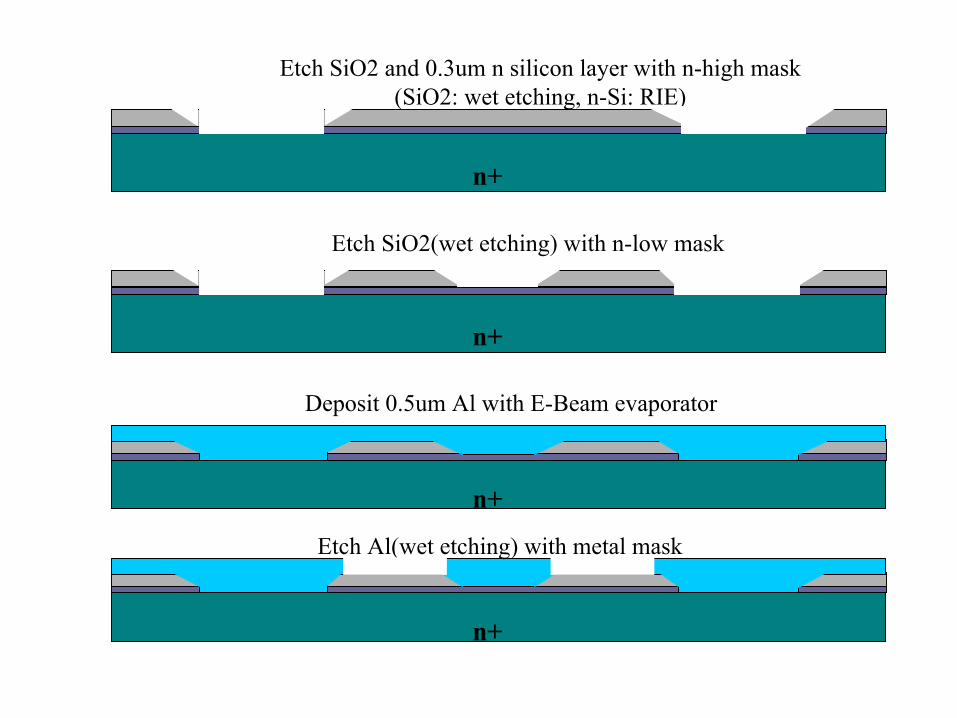
• Mask layout for Schottky diodes• Fabricated Schottky diodes with n+ substrate with n-epi
layer on top• Schottky diodes by CMOS process• RF radiation test• Schottky diodes by using Focused ion beam technology• Schottky diodes designed for MOSIS standard CMOS
process• Conclusion and future work
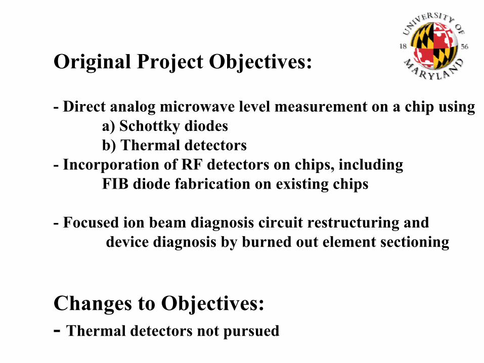
Original Project Objectives:
- Direct analog microwave level measurement on a chip using a) Schottky diodesb) Thermal detectors
- Incorporation of RF detectors on chips, including FIB diode fabrication on existing chips
- Focused ion beam diagnosis circuit restructuring and device diagnosis by burned out element sectioning
Changes to Objectives:- Thermal detectors not pursued
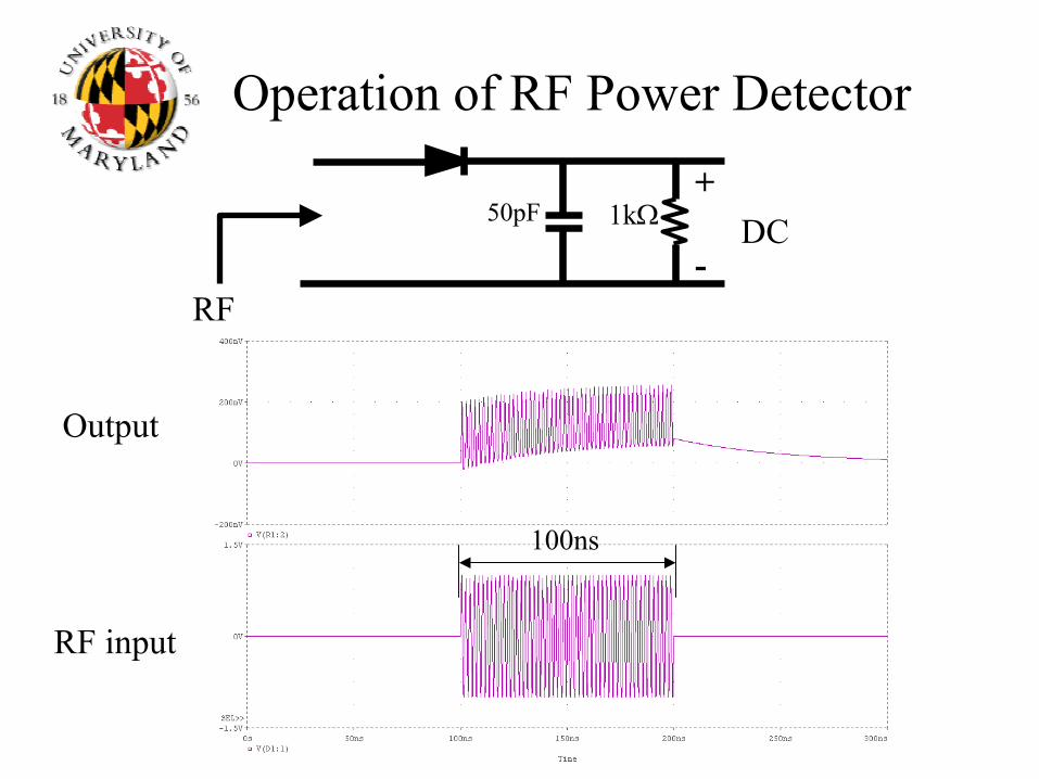
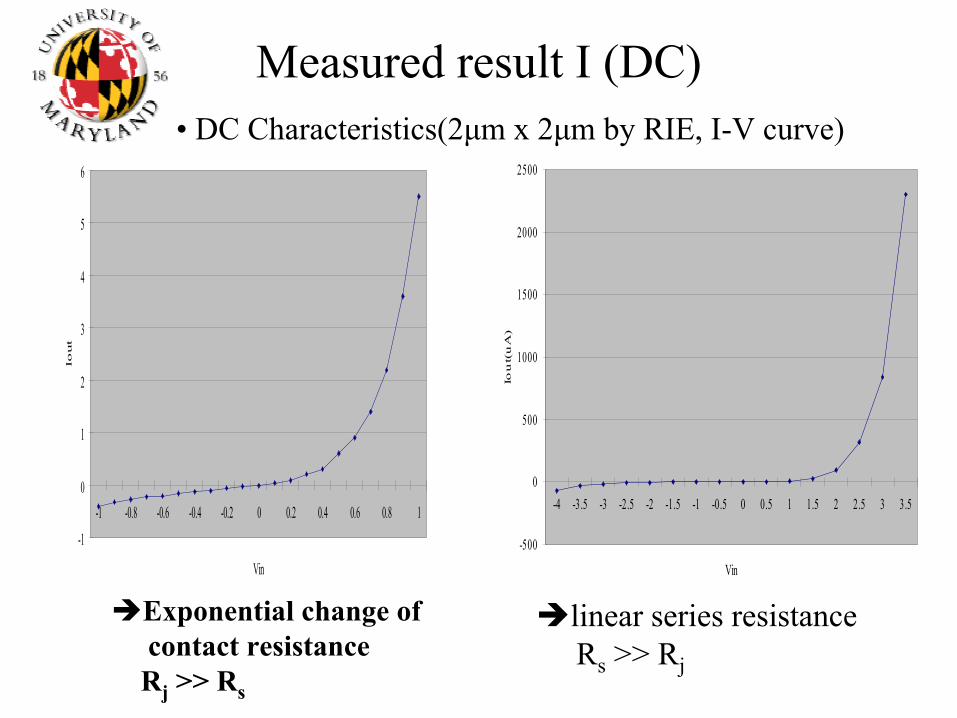
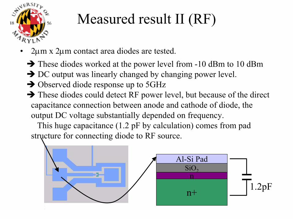
• 2µm x 2µm contact area diodes are tested. These diodes worked at the power level from -10 dBm to 10 dBmDC output was linearly changed by changing power level.Observed diode response up to 5GHz These diodes could detect RF power level, but because of the direct
capacitance connection between anode and cathode of diode, the output DC voltage substantially depended on frequency.
This huge capacitance (1.2 pF by calculation) comes from pad structure for connecting diode to RF source.
n+
nSiO2
Al-Si Pad
1.2pF
Rj: Junction ResistanceCj: Junction capacitanceRs: Series resistance (Rsn + Rs n+ )Co : Overlay capacitance between Al-Si pad and n+ layer
CoRj Cj
Rs
Equivalent circuit
• Overlay capacitance gives direct path between anode and cathode of Schottky diode.
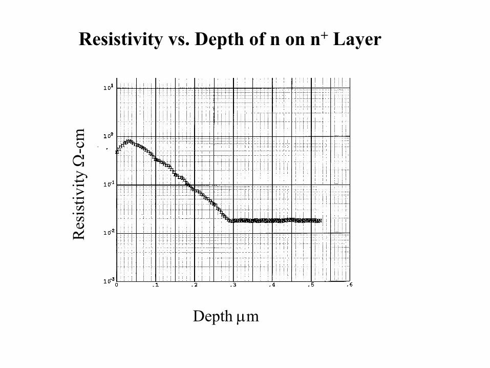
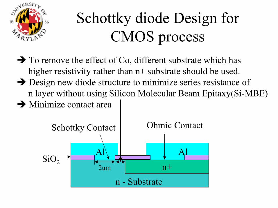
To remove the effect of Co, different substrate which has higher resistivity rather than n+ substrate should be used.Design new diode structure to minimize series resistance of n layer without using Silicon Molecular Beam Epitaxy(Si-MBE)Minimize contact area
Schottky diode Design for CMOS process
n+2um
n - Substrate
Al AlSiO2
Schottky Contact Ohmic Contact
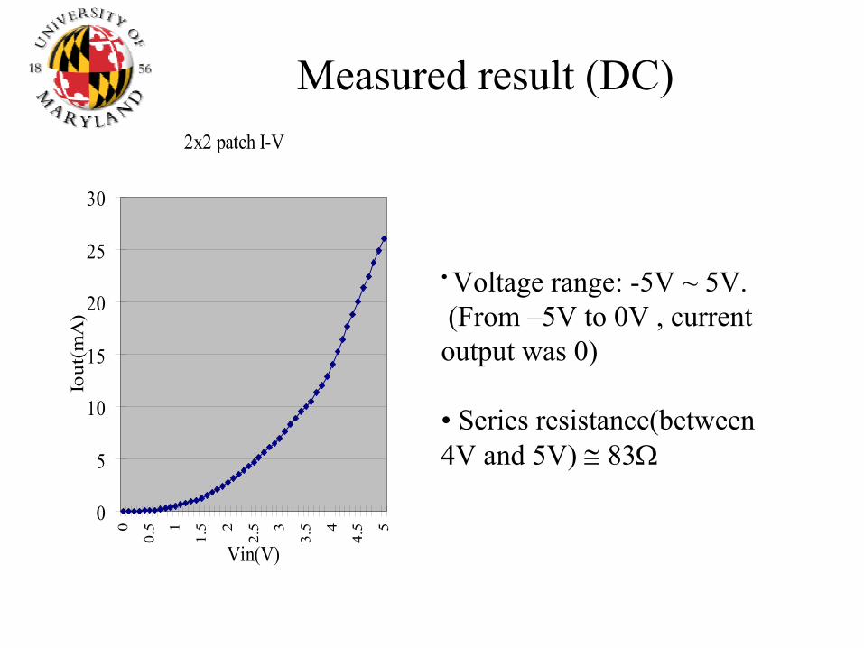
Measured result (DC)2x2 patch I-V
0
5
10
15
20
25
30
0
0.5 1
1.5 2
2.5 3
3.5 4
4.5 5
Vin(V)
Iout
(mA
)
• Voltage range: -5V ~ 5V. (From –5V to 0V , current output was 0)
• Series resistance(between 4V and 5V) ≅ 83Ω
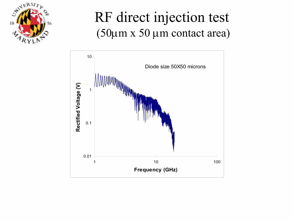
RF direct injection test(50µm x 50 µm contact area)
DC output vs RF Power level
01
23
4
0 5 10 15 20 25
RF power(dBm)O
utp
ut
vo
ltag
e(V
)
RF input:Cascade probe
DC output
GSG
RF direct injection test(2µm x 2 µm contact area)
DC output vs. Power level
00.5
11.5
2
0 5 10 15 20
Power [dBm]
Ou
tpu
t V
olt
ag
e [
V]
5 GHZ 6 GHZDC output vs. Frequency
00.5
11.5
22.5
1 3 5 7 9Frequency(GHz)
Ou
tp
ut v
olt
ag
e(V
)
Flat response at high frequency range
RF direct injection test(50µm x 50 µm contact area)
0.01
0.1
1
10
1 10 100
Frequency (GHz)
Rect
ified
Vol
tage
(V)
Diode size 50X50 microns
-0.01
0
0.010.02
0.03
0.04
0.05
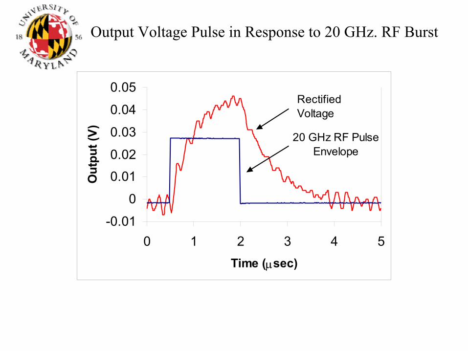
0 1 2 3 4 5Time (µsec)
Out
put (
V) 20 GHz RF Pulse Envelope
Rectified Voltage
Output Voltage Pulse in Response to 20 GHz. RF Burst
-0.10
0.10.20.30.40.50.60.70.8
0 1 2 3 4 5Time (µsec)
Out
put (
V)Rectified Voltage
2GHz RF Pulse Envelope
Output Voltage Pulse in Response to 2GHz.RF Burst
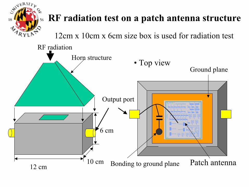
RF radiation test on a patch antenna structure
Horn structureRF radiation
12 cm10 cm
6 cm
12cm x 10cm x 6cm size box is used for radiation test
Output port
• Top viewGround plane
Bonding to ground plane Patch antenna
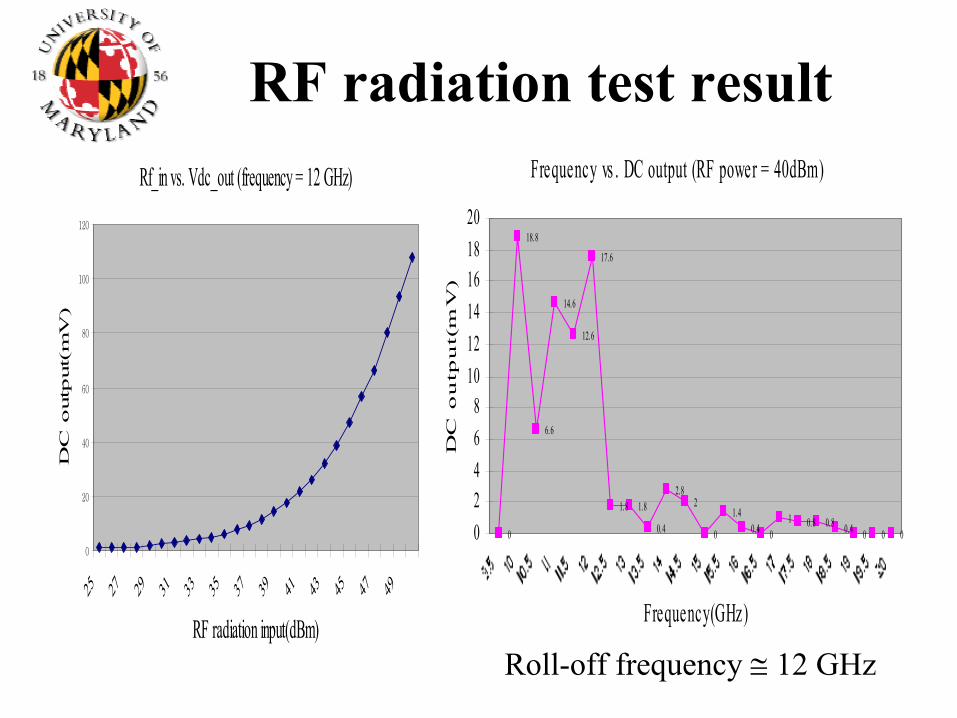
RF radiation test resultRf_in vs. Vdc_out (frequency = 12 GHz)
0
20
40
60
80
100
120
25 27 29 31 33 35 37 39 41 43 45 47 49
RF radiation input(dBm)
DC
outp
ut(
mV
)
Frequency vs . DC output (RF power = 40dBm)
0
18.8
6.6
14.6
12.6
17.6
1.8 1.8
0.4
2.82
0
1.40.4 0
1 0.8 0.8 0.4 0 0 002468
101214161820
Frequency(GHz)
DC
ou
tpu
t(m
V)
Roll-off frequency ≅ 12 GHz
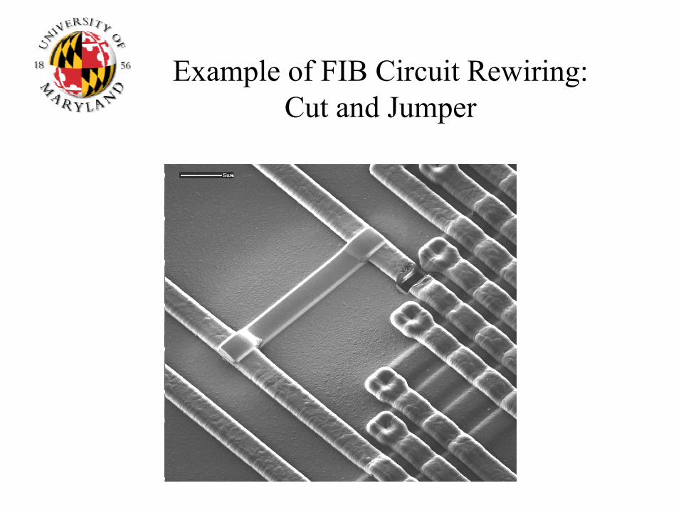
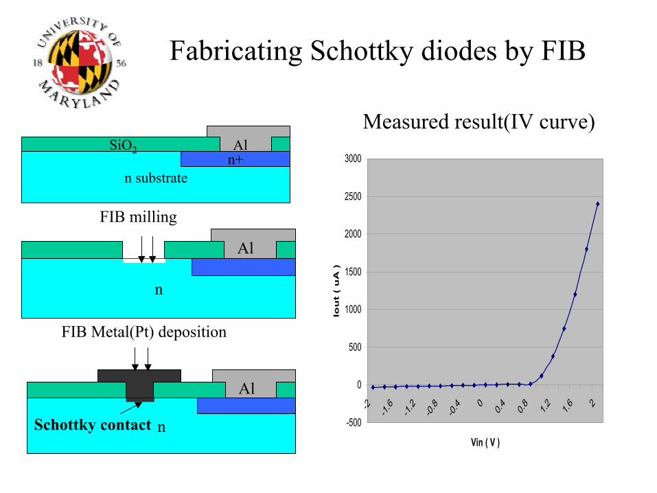
Fabricating Schottky diodes by FIB
n substraten+
SiO2 Al
n
Al
FIB Metal(Pt) deposition
Schottky contact -500
0
500
1000
1500
2000
2500
3000
-2
-1.6
-1.2
-0.8
-0.4 0
0.4
0.8
1.2
1.6 2
Vin ( V )
Iou
t (
uA
)
n
Al
FIB milling
Measured result(IV curve)
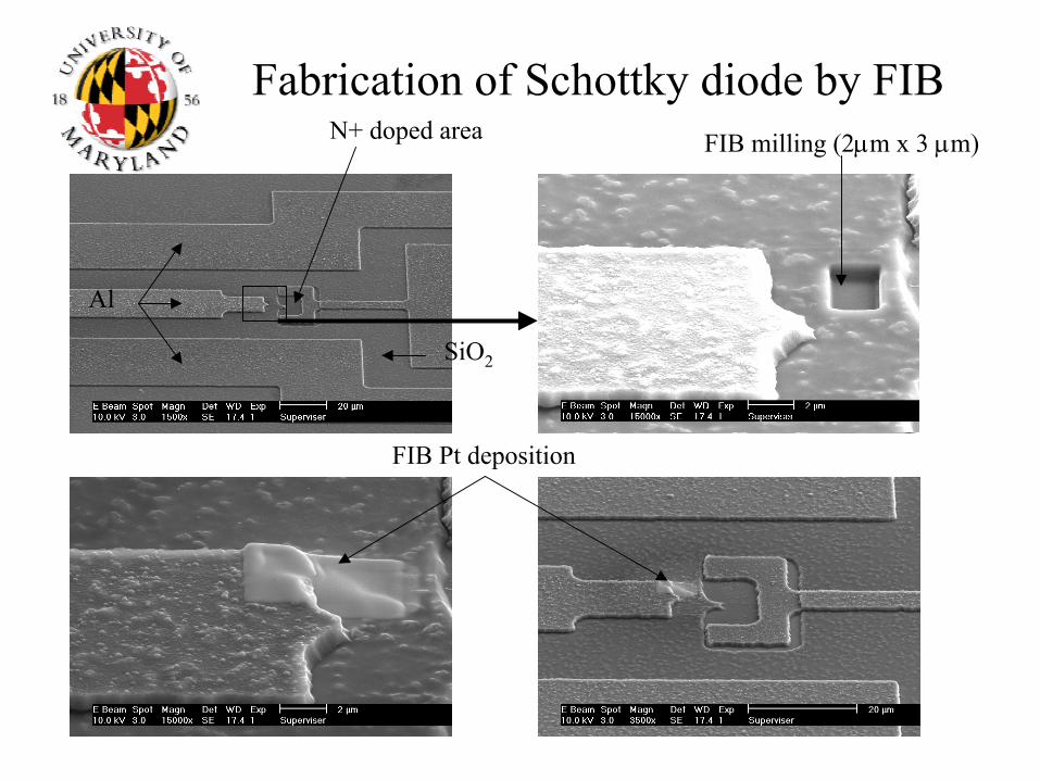
Fabrication of Schottky diode by FIBN+ doped area
Al
SiO2
FIB milling (2µm x 3 µm)
FIB Pt deposition
RF direct injection test of FIB diode
Vout vs. Frequency at 15dBm RF power
0.1
1
10
1 3 5 7 9 11 13 15 17 19 21Frequency(GHz)
Vo
ut (
V)
Vout vs. Frequency sweep Vout vs. RF power sweep
FIB pow er sweep at 8GHz and 10GHz
0
0.5
1
1.5
2
2.5
0 5 10 15 20 25
Injected RF pow er(dBm)
Vo
ut (
V)
8GHz10GHz
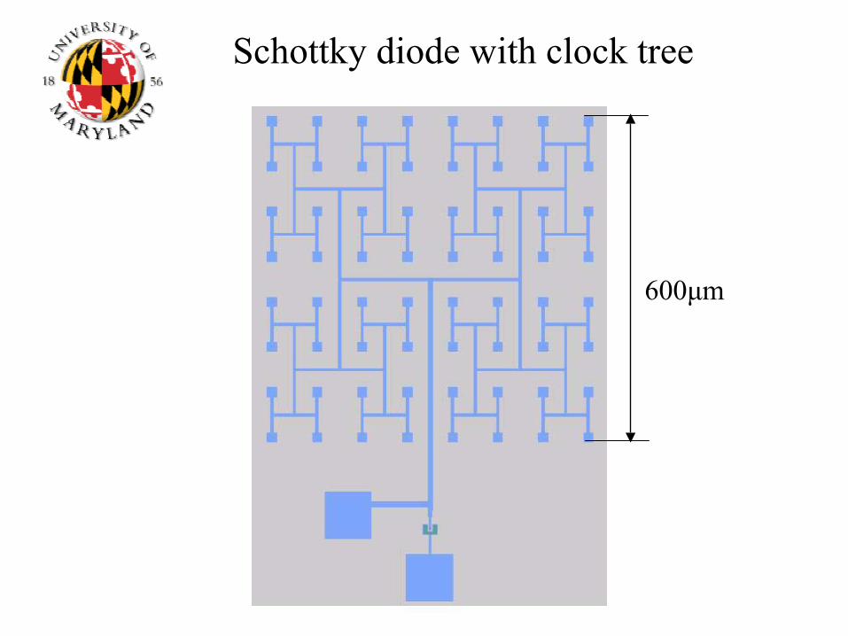
Schottky diodes with capacitor load and MOSFET amp for amplifying small output signal
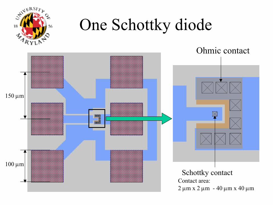
One Schottky diode
100 µm
150 µm
Schottky contactContact area: 2 µm x 2 µm - 40 µm x 40 µm
Ohmic contact
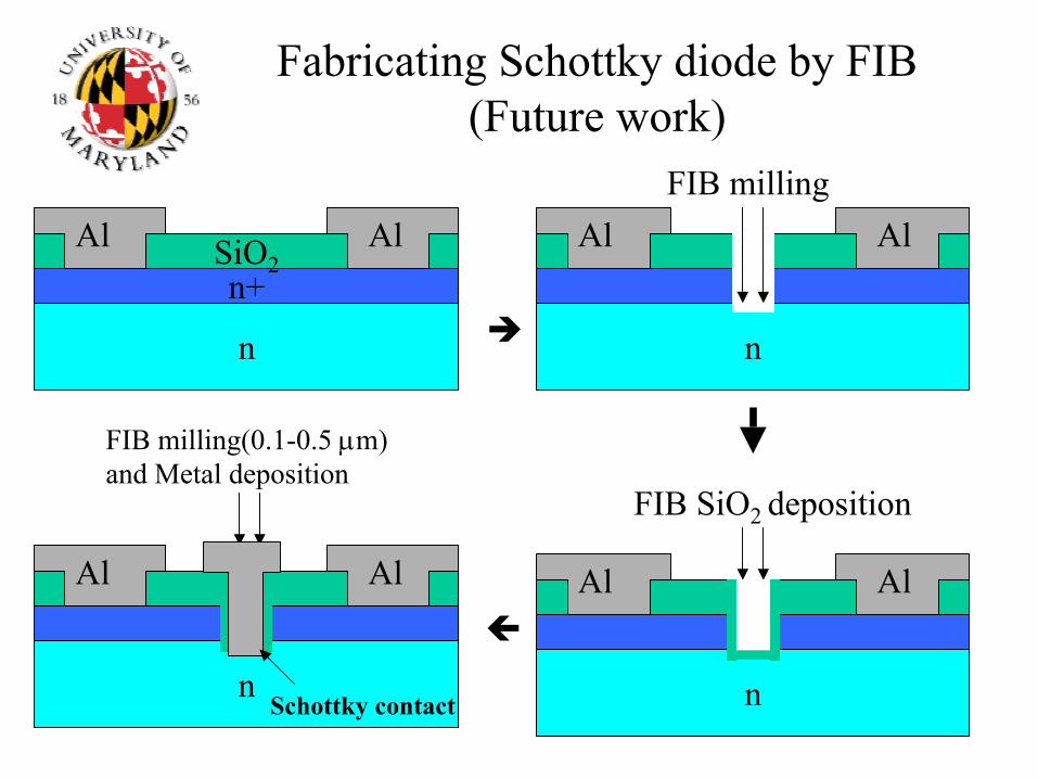
Fabricating Schottky diode by FIB(Future work)
n+
n
SiO2Al Al
n
Al AlFIB milling
n
Al Al
FIB SiO2 deposition
n
Al Al
FIB milling(0.1-0.5 µm)and Metal deposition
Schottky contact
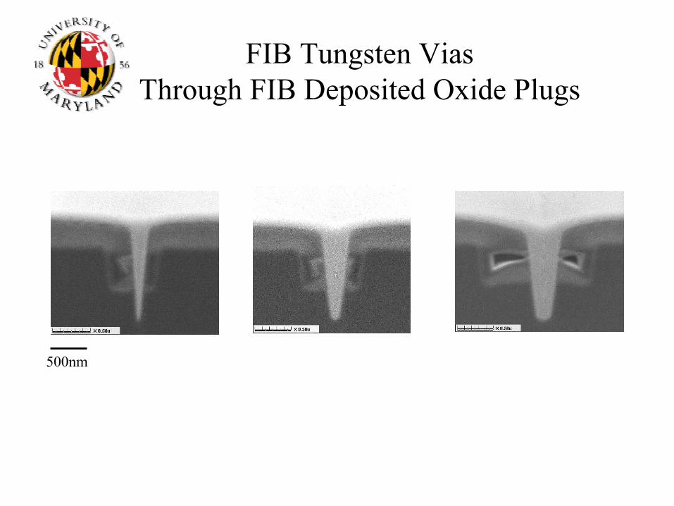
FIB Tungsten Vias Through FIB Deposited Oxide Plugs
500nm
Summary
• Schottky diodes on n-epi and n+ substrate were fabricated and tested
• CMOS process Schottky diodes were designed, fabricated and tested with RF radiation up to 12.5GHz (50X higher than previous CMOS result)and by direct injection up to 20GHz
• Schottky diodes were fabricated by FIB techniques and tested up to 17.5 GHz
• Various Schottky diodes have been designed and submitted to MOSIS for standard CMOS processing
• Paper will be presented at the 2003 International Semiconductor Device Research Symp. in DC
Future work• MOSIS chips now being built will be tested by
RF radiation and direct injection• Post processing MOSIS chips for FIB diodes• Diodes with in-situ amplifiers on chip• Diodes with built in DC bias will be designed
for MOSIS and built• Diodes will be incorporated into test chips
designed by colleagues to verify variousRF propagation models
Understand what limits frequency & push toward 100GHz without MBE