Page 1
Schottky Tunnel Contacts for Efficient Coupling of Photovoltaics and Catalysts
Collaborators: Paul C. McIntyre, Y.W. Chen, J.D. Prange, A. Scheuermann, M. Gunji, O. Hendricks
Support: Precourt Institute for Energy Seed Grant; CIS Seed Funds;
Stanford Graduate Fellowship, NSF Graduate Fellowship, GCEP
Christopher E. D. Chidsey
Department of Chemistry
Stanford University
Page 2
Storage: Energy Density Comparison
2
Pumped Hydro Storage
e.g. pump 1 L of water up the Hoover Dam
Energy density ≈ 1.8 kJ/L
Li Ion Rechargeable Battery
Energy density* ≈ 0.9-2.2 MJ/L
Hydrogen Storage
e.g. H2 in metal hydrides
Energy density ≈ 5-15 MJ/L
Liquid Fuel
e.g. 2 C8H18 + 25 O2 → 16 CO2 + 18 H2O
Energy density ≈ 35 MJ/L
* http://www.greencarcongress.com/2009/12/panasonic-20091225.html ¶ Sorensen, B., Renewable Energy Conversion, Transmission and Storage. Elsevier. (2007)
Page 3
Major Scientific Challenges of
Photoelectrochemical Fuel Synthesis
• Oxidative stability of anode
• Proper alignment of band edges
• Optimizing solar absorption
• Making liquid fuels rather than hydrogen gas
(not addressed in this work)
3
Page 4
-2
-1
0
1
2
0 1 10 11 12 13 14 5 6 7 8 9 3 4 2
pH
Pote
ntial, V
(vs.
NH
E)
TiO2
Ti3+
Ti2O3
Ti
TiO
Water Oxidation
Proton Reduction
Titanium Pourbaix Diagram
Why we want to use Titanium Dioxide
4
Page 5
Photoelectrochemical Electrolysis of Water
• Schematic of solar hydrogen synthesis by photolysis of water using a
semiconducting photoanode with Eg = 3.0 eV (such as TiO2,* SrTiO3).
Basic Research Needs for Solar Energy Utilization, US DOE (2005)
* A. Fujishima and K. Honda, Nature 238, 37-38 (1972). 5
Page 6
Photoanode Selection • Stable semiconductor absorbers tend to have large band gaps
– e.g. TiO2 with 3.4eV
– Only able to absorb UV portion of solar spectrum
Si
Fe2O3
TiO2
A B
M. Grätzel, Nature 414, 338-44 (2001).
6
• Use silicon with a smaller band gap but protect it with larger band gap, corrosion-resistant layer of TiO2.
• Must also control band offsets and add additional voltage.
Page 7
“We disregard in our treatment the special case of such thin layers (<
50 Å)… it is hardly possible to produce such thin layers without
pinholes or larger defects.”
H. Gerisher et. al. (J. Electrochem. Soc., 1983, 130(11), 2173-2179.)
Background – Protecting Si Photoanodes
A. Bard et. al. (J. Electrochem. Soc., 1977, 124(2), 225-229.)
“There does not appear to be any advantage in depositing TiO2
…because of the inability to transfer holes from the substrate through
the TiO2.”
Conclusion: Don’t Use TiO2
Conclusion: Don’t Use Thin Layers
Our Work: Use Thin Layers of TiO2 7
Page 8
Atomic-Layer-Deposition (ALD) Protection of Silicon Electrode
• Combine chemical stability of TiO2 with efficient photo-absorption by Si substrate
• Coat thin TiO2 by ALD as corrosion resistant tunnel oxide
• Deposit thin surface layer of a known water oxidation catalyst (e.g. Ir) H2O(g)
TDMAT(g) Saturated adsorption
HNMe2 (g)
TiO2(s)
8
Y.W. Chen et al., Nature Mater. 10, 539 (2011).
Page 9
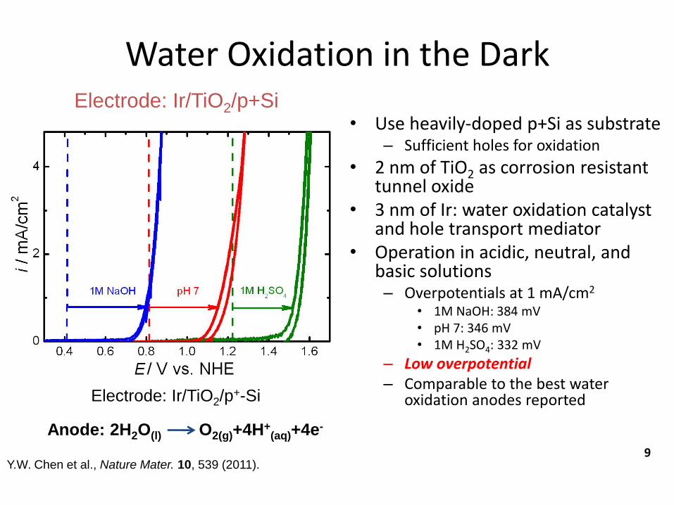
Water Oxidation in the Dark
• Use heavily-doped p+Si as substrate – Sufficient holes for oxidation
• 2 nm of TiO2 as corrosion resistant tunnel oxide
• 3 nm of Ir: water oxidation catalyst and hole transport mediator
• Operation in acidic, neutral, and basic solutions – Overpotentials at 1 mA/cm2
• 1M NaOH: 384 mV • pH 7: 346 mV • 1M H2SO4: 332 mV
– Low overpotential – Comparable to the best water
oxidation anodes reported
Electrode: Ir/TiO2/p+-Si
Electrode: Ir/TiO2/p+Si
9
Anode: 2H2O(l) O2(g)+4H+(aq)+4e-
Y.W. Chen et al., Nature Mater. 10, 539 (2011).
Page 10
• Use lightly-doped n-Si as substrate – Holes must be photo-generated for
efficient oxidation
• Without illumination – No observable peaks
• With AM 1.5 illumination – “Overpotentials” at 1 mA/cm2
• 1M NaOH: -171 mV • pH 7: -219 mV • 1M H2SO4: -200 mV
– Large water oxidation current density below equilibrium (dark) potential
– Inferred photovoltage ≈ 550 mV
Electrode: Ir/TiO2/n-Si
10
Water Oxidation in Simulated Solar Light
Y.W. Chen et al., Nature Mater. 10, 539 (2011).
Page 11
1 M H2SO4
Light Electrolysis – n-Si Substrates
Current saturation under illumination: 26 mA/cm2
Theoretical limit for Silicon: 43 mA/cm2
11
60% charge collection
Page 12
Stability of Anodes – n-Si with Solar Illumination
Hold spot of anode at a constant current of 5 mA/cm2
Samples with TiO2
Samples without TiO2
Samples with TiO2
Samples without TiO2
1 M Base 1 M Acid
12
Page 13
Stability of Anodes – TEM
Before (left) and after (right) images of Ir/TiO2/Si anode for 3 hr stability Test
13 Y.W. Chen et al., Nature Mater. 10, 539 (2011).
Page 14
Stability of Anodes – XPS Depth Profiling After Stability Test – Protection with TiO2
14 Y.W. Chen et al., Nature Mater. 10, 539 (2011).
Page 15
Ir/2 nm TiO2/p+-Si
2 nm TiO2/p+-Si
Electronic Transport Characterization
• Use Fe(CN)63-/Fe(CN)6
4- redox pair to study charge transfer efficiency in electrodes
– Fe(CN)63-/Fe(CN)6
4- redox reaction has low kinetic barrier (Scherer et al., J. Electroanal. Chem., 85, p77, 1977)
• Importance of Ir layer as carrier transport mediator
– No Fe(II)/Fe(III) peaks observed for TiO2/p+-Si samples without Ir top layer
– Large Fe(II)/Fe(III) peak with the thin Ir top layer
– Peak-to-peak splitting similar to conductive electrodes (e.g. ITO)
• Efficient electron transport explained by band structure
– Nearly flat band at equilibrium on p+-Si substrates
15
Page 16
• No oxidation wave observed without illumination – Lack of holes in n-Si in the dark – Have to generate electron-hole
pairs for oxidation reaction to proceed
– Difficult to do with thick Si depletion layer
• Oxidation wave recovers with illumination – Electron-hole pairs supplied by
incident photons
• E0 shifts to the lower potential – Effective photovoltage ~550mV
when compared to the dark CV – Similar to the photovoltage
observed for water oxidation
Ir/2 nm TiO2/n-Si light Ir/2 nm TiO2/p+-Si
Ir/2 nm TiO2/n-Si
Electronic Transport Characterization
16
Page 17
TiO2 Thickness Effects
17
• Amorphous TiO2 as-deposited
• Film thickness can be controlled using ALD cycle number
• Films have smooth interfaces and uniform thickness
A.G. Scheuermann et al., Energy Environ. Sci. DOI: 10.1039/c3ee41178h
Page 18
TiO2 Thickness Effects
• Thin (2 nm) TiO2 has a very small peak-to-peak splitting – ~130 mV
• Thick (10 nm) TiO2 has a much larger peak-to-peak splitting – ~610 mV
• Greater barrier to hole transport through thick TiO2
• ALD enables growth of a thin and pinhole-free TiO2 tunnel oxide – facile carrier transport
Ir/2 nm TiO2/p+-Si
Ir/10 nm TiO2/p+-Si
18 Y.W. Chen et al., Nature Mater. 10, 539 (2011).
• Standard ferri/ferrocyanide redox couple in water
• Peak-to-peak splitting measures barrier to electron
transport from electrode to electrolyte
Page 19
19
0 2 4 6 8 10 120
100
200
300
400
500
600
Base
pH7
Acid
FFC
Overp
ote
ntial (m
V)
TiO2 thickness (nm)
TiO2 Thickness Effects: Overpotential
• Increasing TiO2 thickness requires increasing overpotential
for the same water oxidation rate; ~ 20 mV/nm TiO2
• At very small thicknesses, the overpotential for water splitting
is approximately constant, suggesting it is not limited by
electronic conduction A.G. Scheuermann et al., Energy Environ. Sci. DOI: 10.1039/c3ee41178h
Ir/TiO2/p+Si
Page 20
Conduction Mechanism: Ir Solid State Contact
• Solid-state contact current-voltage measurements – No solution here – p+Si substrate – 50 nm Ir layer as top contact
• Observe tunneling conduction – by varying TiO2 thickness – by varying temperature & applied bias
• Thin TiO2 – Current almost independent of
temperature – Direct tunneling through the ALD-grown
oxide
• Thick TiO2 – Current increases (by several orders of
magnitude) with temperature – Current is thermally activated and bulk
limited 20 Y.W. Chen et al., Nature Mater. 10, 539 (2011).
Applied VG = -0.5 V on Ir contact
Vfb = +0.13 V
Page 21
Solid-State MIS Characterization
21
• Good CV behavior of ultrathin films on p-Si substrate
• No Vfb shift with thickness Low fixed charge in oxide • Predicted shifts with ΦM suggests Fermi-level unpinned
50nm Ir / x TiO2 / native SiO2 / p-Si / 20nm Pt
-0.5
0
0.5
1
1.5
2
Fla
t b
an
d v
olt
ag
e (
V)
Gate Metal
Gate metal effect on Vfb
Theoretical range
Observed
Ir Pt Pd Ni Al -2.0 -1.5 -1.0 -0.5 0.0 0.5 1.0 1.5 2.00.0
0.5
1.0
1.5
2.0
2.5
3.0
Capacitance (
uF
/cm
2)
Gate Bias (V)
800kHz
1nm TiO2
8nm TiO2
-1.2 -0.8 -0.4 0.0 0.4 0.8 1.20.0
0.5
1.0
1.5
2.0
2.5
Ca
pa
cit
an
ce
(u
F/c
m2
)
Gate Bias (V)
1kHz
800kHz
2nm TiO2
/ / A.G. Scheuermann et al., Energy Environ. Sci. DOI: 10.1039/c3ee41178h
Page 22
22
MIS Junction Band Structure1-3
1. M. Perego et al., J. Appl. Phys. 2008, 103, 043509.
2. W. Mönch, J. Appl. Phys. 2010, 107, 013706.
3. M. Houssa et al., J. Appl. Phys. 2000, 87, 8615.
• Bulk-limited electron hopping conduction through the TiO2 layer and tunneling across the ultra-thin SiO2 layer.
• Bulk conduction through TiO2 contributes ~ 20 mV of overpotential increase per nm of thickness at J = 1 mA/cm2
• Corresponds to a bulk resistivity of 2x10⁸ ˑcm
• The bulk resistivity of TiO2 will
depend on its oxygen stoichiometry, crystallinity, etc.
Page 23
23
Conclusions
• Fuels generated from renewable energy can help accommodate
intermittency. -high energy density
• Water is the only readily accessible source of electrons for solar fuel
synthesis at large scale.
• Water oxidation is a kinetically difficult reaction that requires
oxidation stable but catalytically active surfaces.
• Atomic layer deposited tunnel oxides can protect Si and, potentially,
other high-quality semiconductor absorbers so they can be used in
efficient solar-driven water splitting.
• Atomic layer deposition of ultrathin and pinhole-free TiO2 produces a
Schottky tunnel junction coupling a high quality semiconductor to
a nanoscale oxidation catalyst .
• ALD-TiO2 adds only a modest overpotential penalty of 20 mV/nm