IJCSI International Journal of Computer Science Issues, Vol. 2, 2009ISSN (Online): 1694-0784 ISSN (Printed): 1694-0814 33 IJCSI IJCSI Self-Partial and Dynamic Reconfiguration Implementatio n for AES using FPGA Zine El Abidine ALAOUI ISMAILI and Ahmed MOUSSA Innovative Technologies Laboratory, National School of Applied Sciences, Tangier, PBox 1818, Morocco [email protected][email protected]Abstract This paper addresses efficient hardware/software implementat ion approaches for the AES (Advanced Encryption Standard) algorithm and describes the design and performance testing algorithm for embedded system. Also, with the spread of reconfigurable hardware such as FPGAs (Field Programmable Gate Array) embedded cryptographic hardware became cost-effective. Nevertheless, it is worthy to note that nowadays, even hardwired cryptographic algorithms are not so safe. From another side, the self-reconfiguring platform is reported that enables an FPGA to dynamically reconfigure itself under the control of an embedded microprocessor. Hardware acceleration significantly increases the performance of embedded systems built on programmable logic. Allowing a FPGA-based MicroBlaze processor to self-select the coprocessors uses can help reduce area requirements and increase a system's versatility. The architecture proposed in this paper is an optimal hardware implementation algorithm and takes dynamic partially reconfigurable of FPGA. This implementation is good solution to preserve confidentiality and accessibility to the information in the numeric communication. Key words: Cryptography; Embedded systems; Reconfigurable computing; Self-reconfiguration 1.Introduction Today, ultra deep submicronic technologies offer high scale density of integration for communication systems. This growth in integration has been accompanied with dramatically increase of complexity and transaction speed of this systems. As a consequence, security becomes a challenge and a critical issue especially for real time applications where materiel and software resources are very precious and necessary to provide a minimum ofservice quality. Indeed, today speed and computing power impose the recourse to sophisticated and more complicated cryptography algorithms for high level security. Full software implementation is very heavy and slows down considerably speed of the information exchange. From another side, full hardware implementation is very expensive in terms of area, power and can also deteriorate speed of information transitions. This can be done dynamically at run-time and without user interaction, while the static part of the chip is not interrupted. The idea we put into practice is a coarse-grained partially dynamically reconfigurable implementation of a cryptosystem. Our prototype implementation consists of a FPGA which is partially reconfigured at run-time to provide countermeasures against physical attacks. The static part is only configured upon system reset. Some advantages ofdynamic reconfiguration for cryptosystems have been explored before [1, 2, 3]. In such systems, the main goal ofdynamic reconfigurability is to use the available hardware resources in an optimal way. This is the first work that considers using a coarse-grained partially dynamically reconfigurable architecture in cryptosystems to prevent physical attacks by introducing temporal and/or spatial jitter [4, 5]. This paper presents an optimal implementation of the AES (Advanced Encryption Standard) cryptography algorithm by the use of a dynamic partially reconfigurable FPGA [6]. The reconfigurable aspect adapts the allowed basic bloc size to both the loop number and the size of the provided information, and makes all the AES blocs reconfigurable. The paper is organized as follows: section 2 describes the AES algorithm. Reconfigurable FPGA and selfreconfigurable methodology is presented in section 3, 4 and 5. The proposed methodology of algorithm implementation is given in section 6. Finally, results are presented and illustrated in section 7.
Transcript
8/14/2019 Self-Partial and Dynamic Reconfiguration Implementation for AES using FPGA,, IJCSI, Volume 2, August 2009.
This paper addresses efficient hardware/software implementation
approaches for the AES (Advanced Encryption Standard)algorithm and describes the design and performance testingalgorithm for embedded system.
Also, with the spread of reconfigurable hardware such as FPGAs(Field Programmable Gate Array) embedded cryptographichardware became cost-effective. Nevertheless, it is worthy to
note that nowadays, even hardwired cryptographic algorithms arenot so safe.From another side, the self-reconfiguring platform is reported
that enables an FPGA to dynamically reconfigure itself under thecontrol of an embedded microprocessor. Hardware accelerationsignificantly increases the performance of embedded systems
built on programmable logic. Allowing a FPGA-based
MicroBlaze processor to self-select the coprocessors uses canhelp reduce area requirements and increase a system's versatility.
The architecture proposed in this paper is an optimal hardwareimplementation algorithm and takes dynamic partially
reconfigurable of FPGA. This implementation is good solution to preserve confidentiality and accessibility to the information inthe numeric communication.
Today, ultra deep submicronic technologies offer high
scale density of integration for communication systems.
This growth in integration has been accompanied with
dramatically increase of complexity and transaction speedof this systems. As a consequence, security becomes a
challenge and a critical issue especially for real time
applications where materiel and software resources are
very precious and necessary to provide a minimum of service quality.
Indeed, today speed and computing power impose therecourse to sophisticated and more complicated
cryptography algorithms for high level security. Full
software implementation is very heavy and slows down
considerably speed of the information exchange. From
another side, full hardware implementation is veryexpensive in terms of area, power and can also deteriorate
speed of information transitions. This can be done
dynamically at run-time and without user interaction,
while the static part of the chip is not interrupted. The ideawe put into practice is a coarse-grained partially
dynamically reconfigurable implementation of a
cryptosystem.
Our prototype implementation consists of a FPGA which
is partially reconfigured at run-time to provide
countermeasures against physical attacks. The static part isonly configured upon system reset. Some advantages of
dynamic reconfiguration for cryptosystems have been
explored before [1, 2, 3]. In such systems, the main goal of dynamic reconfigurability is to use the available hardwareresources in an optimal way. This is the first work that
considers using a coarse-grained partially dynamically
reconfigurable architecture in cryptosystems to prevent physical attacks by introducing temporal and/or spatial
jitter [4, 5].
This paper presents an optimal implementation of the AES
(Advanced Encryption Standard) cryptography algorithm by the use of a dynamic partially reconfigurable FPGA [6].
The reconfigurable aspect adapts the allowed basic bloc
size to both the loop number and the size of the provided
information, and makes all the AES blocs reconfigurable.The paper is organized as follows: section 2 describes the
AES algorithm. Reconfigurable FPGA and self
reconfigurable methodology is presented in section 3, 4and 5. The proposed methodology of algorithm
implementation is given in section 6. Finally, results are
presented and illustrated in section 7.
8/14/2019 Self-Partial and Dynamic Reconfiguration Implementation for AES using FPGA,, IJCSI, Volume 2, August 2009.
IJCSI International Journal of Computer Science Issues, Vol. 2, 2009 34
IJCSIIJCSI
2. AES Encryption Algorithm
The National Institute of Standards and Technology (NIST)has initiated a process to develop a Federal Information
Processing Standard (FIPS) for the AES, specifying an
Advanced Encryption Algorithm to replace the Data
Encryption Standard (DES) which expired in 1998 [6,7]. NIST has solicited candidate algorithms for inclusion inAES, resulting in fifteen official candidate algorithms of
which five have been selected as finalists. Unlike DES,
which was designed specifically for hardware
implementations, one of the design criteria for AEScandidate algorithms is that they can be efficiently
implemented in both hardware and software. Thus, NIST
has announced that both hardware and software performance measurements will be included in their
efficiency testing. However, prior to the third AES
conference in April 2000, virtually all performance
comparisons have been restricted to software
implementations on various platforms [5]. In October 2000,
NIST chose Rijndael as the Advanced EncryptionAlgorithm.
The AES use the Rijndael encryption algorithm with
cryptography keys of 128, 192, 256 bits. As in most of the
symmetrical encryption algorithms, the AES algorithmmanipulates the 128 bits of the input data, disposed in a 4
by 4 bytes matrix, with byte substitution, bit permutation
and arithmetic operations in finite fields, more specifically,
addition and multiplications in the Galois Field 28
(GF(28 )). Each set of operations is designated by round.
The round computation is repeated 10, 12 or 14 timesdepending on the size of the key (128, 192, 256 bits
respectively). The coding process includes themanipulation of a 128-bit data block through a series of
logical and arithmetic operations. In the computation of
both the encryption and decryption, a well defined order
exists for the several operations that have to be performedover the data block.
The following describes in detail the operation performed
by the AES encryption in each round. The State variable
contains the 128-bit data block to be encrypted. In theEncryption part, first the data block to be encrypted is split
into an array of bytes called as state matrix. This algorithm
is based on round function, and different combinations of
the algorithm are structured by repeating the roundfunction different times. Each round function contains
uniform and parallel four steps: SubBytes, ShiftRows,
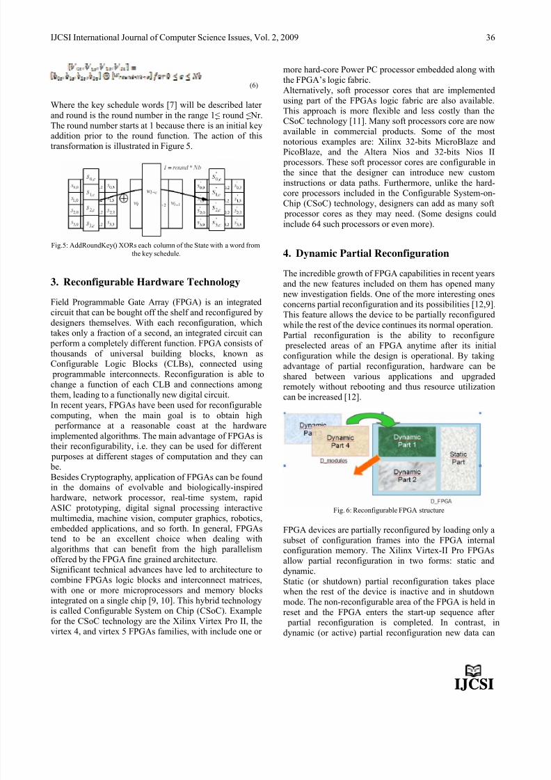
MixColumn and AddRoundKey transformation and eachstep has its own particular functionality. This is
represented by this flow diagram. Here the round key is
derived from the initial key and repeatedly applied to
transform the block of plain text into cipher text blocks.The block and the key lengths can be independently
specified to any multiple of 32 bits, with a minimum of
128 and a maximum of 256 bits. The repeated application
of a round transformation state depends on the block
length and the key length. For various block length and
key length variable’s value are given in table1.The number of rounds of AES algorithm to be performed
during the execution of the algorithm is dependent on the
key size. The number of rounds, Key length and Block Size in the AES standard is summarized in Table 1 [8].
Table 1: Margin specifications Key-Block-Round Combinations for AES
Key length
(Nk round)
Key length
(Bits)
Number of
Round (Nr)
AES-128 4 128 10
AES-192 6 192 12
AES-256 8 256 14
As mentioned before the coding process consists on themanipulation of the 128-bit data block through a series of
logical and arithmetic operations, repeated a fixed number of times. This number of rounds is directly dependent onthe size of the cipher key. In the computation of both the
encryption and decryption, a well defined order exists for
the several operations that have to be performed over thedata block. The encryption/decryption process runs as
embedded applications, and so forth. In general, FPGAstend to be an excellent choice when dealing with
algorithms that can benefit from the high parallelismoffered by the FPGA fine grained architecture.Significant technical advances have led to architecture to
combine FPGAs logic blocks and interconnect matrices,
with one or more microprocessors and memory blocks
integrated on a single chip [9, 10]. This hybrid technologyis called Configurable System on Chip (CSoC). Example
for the CSoC technology are the Xilinx Virtex Pro II, the
virtex 4, and virtex 5 FPGAs families, with include one or
more hard-core Power PC processor embedded along with
the FPGA’s logic fabric.
Alternatively, soft processor cores that are implemented
using part of the FPGAs logic fabric are also available.
This approach is more flexible and less costly than theCSoC technology [11]. Many soft processors core are now
available in commercial products. Some of the most
notorious examples are: Xilinx 32-bits MicroBlaze andPicoBlaze, and the Altera Nios and 32-bits Nios II
processors. These soft processor cores are configurable in
the since that the designer can introduce new custom
instructions or data paths. Furthermore, unlike the hard-core processors included in the Configurable System-on-
Chip (CSoC) technology, designers can add as many soft
processor cores as they may need. (Some designs could
include 64 such processors or even more).
4. Dynamic Partial Reconfiguration
The incredible growth of FPGA capabilities in recent yearsand the new features included on them has opened many
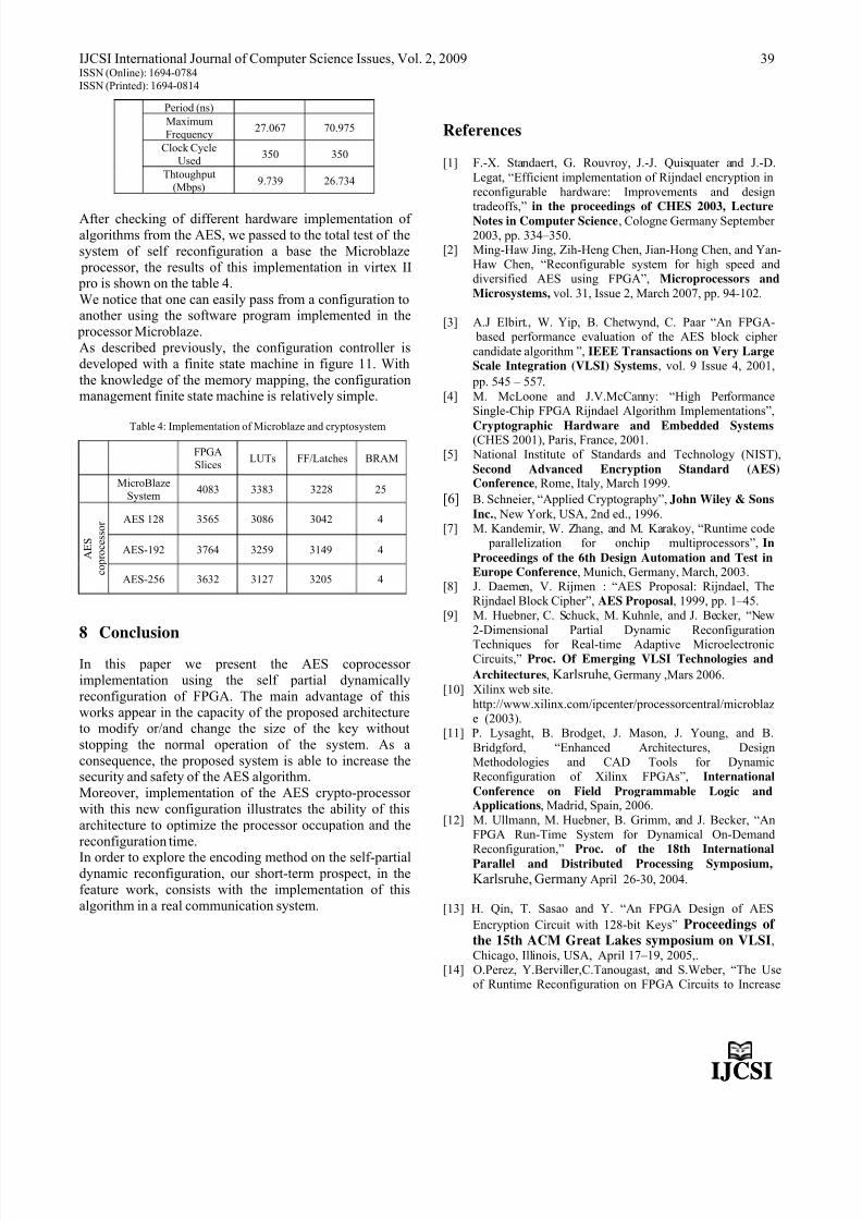
new investigation fields. One of the more interesting onesconcerns partial reconfiguration and its possibilities [12,9].
This feature allows the device to be partially reconfigured
while the rest of the device continues its normal operation.Partial reconfiguration is the ability to reconfigure
preselected areas of an FPGA anytime after its initial
configuration while the design is operational. By taking
advantage of partial reconfiguration, hardware can be
shared between various applications and upgradedremotely without rebooting and thus resource utilization
can be increased [12].
Fig. 6: Reconfigurable FPGA structure
FPGA devices are partially reconfigured by loading only a
subset of configuration frames into the FPGA internalconfiguration memory. The Xilinx Virtex-II Pro FPGAs
allow partial reconfiguration in two forms: static and
dynamic.
Static (or shutdown) partial reconfiguration takes placewhen the rest of the device is inactive and in shutdown
mode. The non-reconfigurable area of the FPGA is held in
reset and the FPGA enters the start-up sequence after partial reconfiguration is completed. In contrast, in
dynamic (or active) partial reconfiguration new data can
8/14/2019 Self-Partial and Dynamic Reconfiguration Implementation for AES using FPGA,, IJCSI, Volume 2, August 2009.
IJCSI International Journal of Computer Science Issues, Vol. 2, 2009
ISSN (Online): 1694-0784
ISSN (Printed): 1694-0814
39
IJCSIIJCSI
Period (ns)
Maximum
Frequency27.067 70.975
Clock Cycle
Used350 350
Thtoughput
(Mbps)9.739 26.734
After checking of different hardware implementation of algorithms from the AES, we passed to the total test of the
system of self reconfiguration a base the Microblaze
processor, the results of this implementation in virtex II pro is shown on the table 4.
We notice that one can easily pass from a configuration toanother using the software program implemented in the
processor Microblaze.
As described previously, the configuration controller is
developed with a finite state machine in figure 11. With
the knowledge of the memory mapping, the configurationmanagement finite state machine is relatively simple.
Table 4: Implementation of Microblaze and cryptosystem
FPGA
SlicesLUTs FF/Latches BRAM
MicroBlaze
System4083 3383 3228 25
AES 128 3565 3086 3042 4
AES-192 3764 3259 3149 4 A E S
c o p r o c e s s o r
AES-256 3632 3127 3205 4
8 Conclusion
In this paper we present the AES coprocessor
implementation using the self partial dynamically
reconfiguration of FPGA. The main advantage of this
works appear in the capacity of the proposed architectureto modify or/and change the size of the key without
stopping the normal operation of the system. As a
consequence, the proposed system is able to increase thesecurity and safety of the AES algorithm.
Moreover, implementation of the AES crypto-processor
with this new configuration illustrates the ability of this
architecture to optimize the processor occupation and the
reconfiguration time.
In order to explore the encoding method on the self-partialdynamic reconfiguration, our short-term prospect, in the
feature work, consists with the implementation of this
algorithm in a real communication system.
References
[1] F.-X. Standaert, G. Rouvroy, J.-J. Quisquater and J.-D.
Legat, “Efficient implementation of Rijndael encryption inreconfigurable hardware: Improvements and designtradeoffs,” in the proceedings of CHES 2003, Lecture
Notes in Computer Science, Cologne Germany September 2003, pp. 334–350.
[2] Ming-Haw Jing, Zih-Heng Chen, Jian-Hong Chen, and Yan-Haw Chen, “Reconfigurable system for high speed anddiversified AES using FPGA”, Microprocessors and
Microsystems, vol. 31, Issue 2, March 2007, pp. 94-102.
[3] A.J Elbirt., W. Yip, B. Chetwynd, C. Paar “An FPGA- based performance evaluation of the AES block cipher
candidate algorithm ”, IEEE Transactions on Very Large
IJCSI International Journal of Computer Science Issues, Vol. 2, 2009 40
IJCSIIJCSI
the Performance of the AES Algorithm Implementation”,Journal of Universal Computer Science, vol. 13, no. 3,
2007, pp.349-362.[15] N. Saqib, F.Rodriguez-Henriquez, and A. Diaz-Pérez, “Two
approaches for a single-Chip FPGA Implementation of an
Encyptor/Decryptor AES Core” International C-
Conference on Field-Programmable Logic and
Applications , Lisbon , Portugal, September 2003 .[16] M Mogollon: “Cryptography and Security Services:
Mechanisms and Applications” Cybertech Publishing,2007.
[17] Z.A, Alaoui, A. Moussa, A. Elmourabit and K. Amechnoue“Flexible Hardware Architecture for AES Cryptography Algorithm” IEEE Conference on Multimedia Computing
and Systems, ouarzazate, morocco, April 2009.
Z. alaoui-Ismaili, received the DEA in electronics in 1997 andthe Ph.D. degree in Electronics and industrial ComputerEngineering in 2002, both from University IbnTofail de Kenitra,Morocco. He is currently researcher teacher at the Telecoms &
Electronics department of National School of Applied Sciencestangier, Morocco, since June 2003.His main research interests are FPGA based reconfigurablecomputing applications, with a special focus on dynamic partialreconfiguration and embedded systems.Dr. Alaoui_Ismaili authored or coauthored more than 10 papers journal and conference.He is president of Association Moroccan Society ofmicroelectronics.
A. Moussa, was born in 1970 in Oujda, Morocco. He receivedthe Licence in Electronics from the University of Oujda, Morocco,in 1994, and the PhD in Automatic Control and InformationTheory from the University of Kenitra, Morocco, in 2001. Heworked two years as a post-graduate researcher at theUniversity of Sciences and Technology of Lille, France. At 2003he joined Sanofi-Aventis research laboratory in Montpellier,
France where he supervised Microarray analysis activities .He isnow a professor at the National School of Applied Sciences inTangier-Morocco and his current research interests are in theapplication of the Markov theory and multidimensional dataanalysis to image processing, and embedded systems.