1 Semiconductor Flash Memory Scaling by Min She B.S. (University of Science and Technology of China) 1996 M.S. (Johns Hopkins University) 1997 A dissertation submitted in partial satisfaction of the requirements for the degree of Doctor of Philosophy in Engineering-Electrical Engineering and Computer Sciences in the GRADUATE DEVISION of the UVIVERSITY OF CALIFORNIA, BERKELEY Committee in charge: Professor Tsu-Jae King, Chair Professor Vivek Subramanian Professor Timothy Sands Fall 2003
Transcript
1
Semiconductor Flash Memory Scaling
by
Min She
B.S. (University of Science and Technology of China) 1996 M.S. (Johns Hopkins University) 1997
A dissertation submitted in partial satisfaction of the
requirements for the degree of
Doctor of Philosophy
in
Engineering-Electrical Engineering and Computer Sciences
in the
GRADUATE DEVISION
of the
UVIVERSITY OF CALIFORNIA, BERKELEY
Committee in charge:
Professor Tsu-Jae King, Chair Professor Vivek Subramanian
Professor Timothy Sands
Fall 2003
2
The dissertation of Min She is approved:
University of California, Berkeley
Fall 2003
Chair Date
Date
Date
3
Semiconductor Flash Memory Scaling
Copyright 2003
by
Min She
4
Abstract
Semiconductor Flash Memory Scaling
by
Min She
Doctor of Philosophy in Engineering -
Electrical Engineering and Computer Sciences
University of California, Berkeley
Professor Tsu-Jae King, Chair
Semiconductor flash memory is an indispensable component of modern electronic
systems. The minimum feature size of an individual CMOSFET has shrunk to 15nm with
an equivalent gate oxide thickness (EOT) of 0.8nm in 2001. However, semiconductor
flash memory scaling is far behind CMOS logic device scaling. For example, the EOT of
the gate stack in semiconductor flash memory is still more than 10nm. Moreover,
semiconductor flash memory still requires operation voltage of more than 10V, while the
operation voltage of CMOS logic has been scaled to 1V or even less.
This dissertation addresses the issue of gate stack scaling and voltage scaling for
future generations of semiconductor flash memory, and proposes solutions based on new
memory structure and new materials that are compatible with the current CMOS process
flow. Chapter 1 discusses the key challenges in scaling flash memories. In chapter 2, a
theoretical model that accounts for both the Coulomb blockade effect and the quantum
confinement effect is proposed to model semiconductor nanocrystal memory. The
program/erase speed and retention time in terms of nanocrystal size, tunnel oxide
5
thickness, and different tunnel material other than silicon oxide has been investigated.
Semiconductor nanocrystal memory is shown to have the potential to replace the
conventional floating gate flash memory. Chapter 3 demonstrates that high quality silicon
nitride can be used as the tunnel dielectric to enhance the programming speed, since it
offers a low injection barrier as compared to silicon oxide tunnel dielectric. Retention
time is also enhanced due to the fact that thick tunnel nitride can be used for the same
EOT. In Chapter 4, Hafnium oxide was investigated to replace silicon nitride as the
charge trap/storage layer in SONOS (silicon-oxide-nitride-oxide-silicon) type trap-based
memory. Since the conduction band offset between Hafnium oxide and tunnel oxide is
larger than that between silicon nitride and tunnel oxide, the tunnel barrier from the
charge trap layer is reduced/eliminated during programming; fast programming speed
was achieved with Hafnium oxide trap layer experimentally. The large conduction band
offset can also improve the retention time. New device structures are also indispensable
in making flash memory more scalable. In Chapter 5, a FinFET SONOS flash memory
device has been demonstrated. Its channel length is scalable to 40nm. The experimental
results showed that the FinFET SONOS memory exhibited good program/erase speed,
high endurance and good reading disturbance. It is a suitable embedded memory for the
future FinFET circuit. FinFET memory can achieve a much smaller cell size than that
Dunga, Hei Kam, Dr. Jin He, Dr. Jane Xuemei Xi, Dr. Jun Lin, for their friendship and
support.
I would like to thank Professor Yi Shi at Nanjing University, China, Professor Shinji
Nozaki at University of Electro-Communications, Japan and Professor Tso-Ping Ma at
Yale University for the discussion, help and collaboration. Their supports made my
research life enjoyable.
I would like to thank my family for their love, support and encouragement,
especially to my grandmother for the wonderful childhood I spent with her.
11
Chapter 1
Introduction
1.1 Semiconductor memory comparison
Semiconductor memory is an indispensable component of modern electronic
systems. It is used in personal computers, cellular phones, digital cameras, smart-media,
networks, automotive systems, global positioning systems. Table 1.1 lists the
characteristics of different types of semiconductor memory that either have been
commercialized or are being developed in the industry.
Static Random Access Memory (SRAM) is used as a cache memory in personal
computers since it offers the fastest write/read (8ns) speed among all memories.
However, a single SRAM cell consists of 6 transistors (6T), so SRAM chip density is
very low, although 4T SRAM cells have been demonstrated [1]. SRAM memory can
retain the stored information as long as the power is on, drawing very little current.
However, the information will be lost when the power is turned off, so SRAM is not a
nonvolatile memory.
A Dynamic Random Access Memory (DRAM) cell consists of one transistor and one
capacitor (1T1C). It is superior to SRAM in many aspects except that the write speed is
slower in the DRAM (50ns) than in the SRAM. However, its cell size is much smaller
than that of SRAM and thus it is a low cost commodity memory device. Compared to
12
flash memory, DRAM has much faster program/read speed with very low operating
voltage, while flash memory needs 1us to 1ms programming time and high programming
voltage. Unfortunately, DRAM is a volatile memory. The data retention time is about
100ms in DRAM while it is 10 years in flash memory: a DRAM cell needs refreshing
frequently to maintain its data, so its power consumption is significant. Furthermore, the
size of a DRAM cell is larger than that of a flash memory cell. Scaling the DRAM cell
size down is difficult due to the large capacitor required to store data.
In the past decade, memory chips with low power consumption and low cost have
attracted more and more attention due to the booming market of portable electronic
devices such as cellular phones and digital cameras. These applications require the
memory to have ten years data retention time, so that the nonvolatile memory device has
become indispensable. There are mainly four types of nonvolatile memory technology:
flash memory, Ferro-electric Random Access Memory (FeRAM*), Magnetic Random
Access Memory (MRAM) and phase change memory. Flash memory is presently the
most suitable choice for nonvolatile applications for the following reasons:
1) Flash memory can achieve the highest chip density. A flash memory cell consists
of only one transistor [2]. A FeRAM memory cell generally consists of one transistor
and one capacitor [3], while a MRAM cell needs a transistor and a magnetic tunnel
junction [1]. Phase change memory was expected to be a promising nonvolatile
memory [5]; however, its memory cell consists of one resistor and a bipolar junction
transistor. Until now, only a 4MB phase change memory chip has been demonstrated.
It will take more effort to demonstrate whether the phase change memory is really a
promising technology.
*FeRAM is not a perfect nonvolatile memory since its reading mode is destructive. A programming verification is required to restore the data after reading.
3D potential No No Possible Possible ? ? No SER susceptibility
Yes Yes No No Yes No No
Relative cost per bit
Low High Medium Medium High ? Low
Extra mask needed for embedded memory
6-8 2 4 3-4
In production Yes yes Yes Yes Yes 2004 N/A
Table 1.1: Performance Comparison between volatile memory (DRAM and SRAM) and nonvolatile memory (Flash, FRAM, MRAM and phase change memory) devices. Among the nonvolatile memories, flash memory is the only memory compatible with the current CMOS process flow. Overall, the flash memory exhibits the best performance except for the disadvantages of high programming voltage and slow program/erase speed.
14
2) Flash memory possesses the multi-bit per cell storage property [6]. Four distinct
threshold voltage (VT) states can be achieved in a flash memory cell by controlling the
amount of charge stored in its floating gate. Two-bits/cell (with four VT states) flash
memory cells have already been commercialized. A four-bits/cell flash memory device
is feasible and is under development now [7]. Multi-bit storage increases memory
density and thus reduces the cost per bit significantly. Furthermore, Matrix
Semiconductor Inc. demonstrated multi- layer (sometimes called “three-dimensional
integration”) SONOS flash memory recently [8]. This novel idea offers another
possibility to achieve even higher density and lower cost technologies based on flash
memory.
A 2GB NAND-type flash memory chip has been demonstrated in [9]. A plot of the
NOR-type flash memory cell size versus technology generation is shown in Fig1.1
(with FeRAM as a comparison). At the 130nm generation, a FeRAM memory cell is
160 140 120 100 80 60 40 20
0.01
0.1
1
10
solution NOT known
year of 2004
In production
Cel
l siz
e (u
m2 )
Technology node(nm)
Flash NOR FeRAM
Figure 1.1: Cell size comparison between flash memory and FeRAM. Flash memory has the smallest cell size among all of the nonvolatile memories. The data is from the 2002 International Technology Roadmap for Semiconductors.
15
as 26 times larger than its flash memory counterpart.
3) Flash memory fabrication process is compatible with the current CMOS process
and is a suitable solution for embedded memory applications. A flash memory cell is
simply a MOSFET cell, except that a poly-silicon floating gate [10] (or Silicon Nitride
charge trap layer [8]) is sandwiched between a tunnel oxide and an inter-poly oxide to
form a charge storage layer. All other nonvolatile memories require integration of new
materials that are not as compatible with a conventional CMOS process. It is easier
and more reliable to integrate flash memory than other nonvolatile memories with
logic and analog devices in order to achieve better chip performance for wireless
communication and wireless computation [11].
Since flash memory possesses these three key advantages, it has become the
mainstream nonvolatile memory device nowadays.
However, flash memory exhibits some evident disadvantages as shown in Table 1.1:
the device has a slow program/erase speed and requires a high voltages to program/erase
its data. Additionally, its endurance also needs to be improved, although 105
program/erase cycles is enough for most applications. This thesis will investigate several
ways to improve the program/erase speed and reduce the operation voltage.
1.2 Semiconductor flash memory scaling
The minimum feature size of an individual CMOSFET has shrunk to 15nm with an
equivalent gate oxide thickness (EOT) of 0.8nm in 2001, [12]. However, semiconductor flash
memory scaling is far behind CMOS logic device scaling. For example, the EOT of the gate stack
in semiconductor flash memory is still more than 10nm. Moreover, semiconductor flash memory
16
still requires operation voltages of more than 10V, while the operation voltage of CMOS logic has
been scaled to about 1V or even less.
It is important to scale the EOT of the gate stack to achieve a small memory cell size,
and also prolong battery life. A floating gate flash memory structure is shown in Fig 1.2.
The gate stack consists of an 8nm thermal oxide as the tunnel layer, a 150nm poly-silicon
floating gate and a 13nm (EOT) inter-poly oxide layer [10]. The EOT of the whole gate
stack is 21nm. A typical drain bias is 2V in the reading mode and 4.5V in the
programming mode. This memory cell suffers from serious short channel effects when
the channel length is scaled to sub 100nm, since the EOT of the gate stack is very thick
and the drain bias is relatively large. Both the drain- induced barrier lowering (DIBL)
effect and the sub-surface punch-through effect induce significant leakage current during
reading and programming. As shown in Fig 1.3, the leakage current contributed by the
unselected cells along the same bit line may be so significant that the sensing circuit
thinks the selected cell is at a low threshold voltage (VT) state (with high reading current)
although the selected cell actually is at a high VT state (with low reading current). During
programming, the leakage current may be very significant so that it causes significant
power consumption.
Tunnel oxide
Interpoly dielectric
Well
Drain Source
Control Gate
Floating Gate
Figure 1.2: Schematic cross-section of a floating gate memory device. It is essentially a MOSFET, except that a floating gate is sandwiched between a tunnel oxide and an inter-poly oxide. The tunnel oxide must be thicker than 8nm to maintain 10 years retention time at 85oC.
17
The high voltages required for operation inhibit memory chip density improvement.
A flash memory chip consists of two parts: the core memory cells, and the peripheral
micro-controller circuit. Many high voltage transistors are used in the peripheral circuit to
produce the high voltage required to program/erase the core memory cells. These high
voltage transistors consume a lot of area. In the 0.18um technology generation, the
peripheral circuit occupies an area on the chip that is comparable to the area required for
the core memory. The peripheral circuit scales more slowly than the core memory, since
the operation voltages have not been scaled down over the past several technology
generations. The peripheral circuit also consumes a lot of power to generate the high
voltage.
2V
2V
WL i-1
WL i
WL i+1
BL j-1 BL j BL j+1
Selected cell Unselected cell
Figure 1.3: Word line (WL) i and bit line (BL) j are biased in reading mode to read the selected memory cell (i, j). The current leakage from the unselected cells along the same bit line j may contribute significant current to cause a wrong reading of cell (i, j).
18
Furthermore, the high voltage operation has a direct impact on the core memory
array scaling. Fig 1.4 shows the NROM memory array layout [13]. The poly-silicon
word lines (WL) should be patterned as close as possible to each other to reduce the
memory array size. Unfortunately, the poly-silicon word lines will suffer serious
capacitive coupling when the spacing between them is reduced. Since the poly-silicon
word line is usually very long (several tens of microns), the cross coupling is very strong.
If either word line i-1 or word line i+1 is turned on (or both word lines are on at the same
WL i-1
BL j+1
WL i WL i+1
BL j
BL j-1
100nm
Selected cell Unselected cell
Figure 1.4: The spacing (100nm shown in the figure) between the word lines has to be scaled down further to increase the core memory density. During programming of the selected cell (WL i-1 biased at 10V), word line i is also turned on due to capacitive coupling, so the unselected cell is also programmed. This cross coupling is more severe as the spacing between word lines is decreased, thus limiting the scalability of the word line spacing.
19
time), word line i will be turned on too, due to the cross coupling effect. Then, the
unselected cell will be erroneously programmed.
The scaling of the gate stack and operation voltages are often related to each other.
A tunnel oxide thickness of more than 8nm is currently used in the commercial flash
memory chip to meet the ten years data retention time requirement. If the tunnel oxide
were to be scaled below 2nm, the operation voltage could be reduced from more than
10V to below 4V [14]. Unfortunately, the retention time would also be reduced, from 10
years to several seconds.
Technology node (nm) 90 65 50 35 25 Flash NOR Lg(um) Flash NOR highest W/E voltage (V) 7-9 7-9 7-9 7-9 7-9 Flash NAND highest Voltage (V) 17-19 15-17 15-17 15-17 15-17 NOR tunnel oxide(nm) NAND tunnel oxide(nm) 7-8
0.2-0.22 0.19-0.21 0.17-0.19 0.14-0.16 0.12-0.14
6-7 6-7 6-7 6-7
8.5-9.5 8-9 8-9 8 8
Solution known Solution exist Solution NOT known
Year of production 2004 2007 2010 2013 2016
Table 1.2: Tunnel oxide and operation voltage scaling predicted by the 2002 International Technology Roadmap for Semiconductors.
20
Table 1.2 shows the 2002 International Technology Roadmap for Semiconductor
flash memory [15]. The channel length of the NOR type flash memory will still be longer
than 100nm by the year 2016. Short channel effects prevent the channel length from
being aggressively scaled. The operation voltage and the tunnel oxide will not scale at all
in the coming five technology generations.
1.3 Organization
This dissertation addresses the aforementioned issue of gate stack scaling for
future generations of semiconductor flash memory, and proposes solutions based on new
memory structures and new materials that are compatible with the current CMOS process
flow. Chapter 2 discusses the scaling limit of semiconductor nanocrystal memory
devices. After an introduction of the general scaling requirement for tunnel oxide, a
theoretical model taking into account the quantum confinement effect and the Coulomb
blockade effect is proposed to explain the program/erase and retention characteristics of a
nanocrystal memory. The effect of nanocrystal size, tunnel oxide thickness and tunnel
material on the device performance is investigated. It is concluded that semiconductor
nanocrystal memory is a promising nonvola tile memory although a more delicate
fabrication method is required to achieve uniform nanocrystal size.
In Chapter 3, high quality Jet vapor deposited (JVD) silicon nitride is proposed as a
tunnel dielectric in floating gate flash memory. The hot electron injection barrier at the
interface between the JVD nitride and the silicon substrate is 2.12eV, which is much
lower than the 3.15eV injection barrier offered by a thermal silicon oxide tunnel
dielectric. More efficient electron injection is expected during programming with JVD
21
nitride tunnel dielectric. After hot carrier injection efficiency is discussed, the device
operation principle and fabrication process are shown. Then, the device performance is
presented. A comparison between JVD nitride and thermal oxide as a tunnel dielectric is
made in terms of program/erase speed, retention, programming disturbance and so on.
High quality silicon nitride can also be a tunnel dielectric in a trap-based flash
memory. In Chapter 3, thermal silicon nitride is used as a tunnel dielectric in a SONOS-
type (polysilicon-oxide-nitride-oxide-silicon) memory device. The principle of silicon
nitride as the tunnel dielectric in trap-based memory is different from the JVD nitride as
the tunnel dielectric in floating gate flash memory. The device fabrication and
characterization are presented. Although the thermal silicon nitride is thinner than
required due to fabrication limitations (so the memory is not nonvolatile), initial results
show that high quality silicon nitride can still be a promising tunnel dielectric for trap-
based nonvolatile memory applications.
Instead of scaling the tunnel oxide, new charge trap/storage materials can also be
used to improve the programming speed at low operation voltage and improve the
retention at the same time. In Chapter 4, a high electron affinity, high-K dielectric is
investigated as a charge trap layer to replace the conventional LPCVD silicon nitride trap
layer in the SONOS-type flash memory. To be integrated in flash memories, these new
charge trap materials should be thermally stable during high temperature processes, in
addition to providing deep trap energy levels and sufficient trap density. A memory
device with hafnium oxide charge trap layer shows faster programming speed than a
device with silicon nitride charge trap layer and good retention.
22
Chapter 5 proposes a double-gate “FinFET” SONOS flash memory for embedded
silicon-on- insulator (SOI) application. The FinFET flash memory demonstrates similar
performance as the bulk SONOS flash memory, although there is no body contact in the
FinFET device. Good sub-threshold swing is achieved with the FinFET structure, so that
the ratio of reading current between the selected cell and the unselected cell is increased.
Memory devices fabricated with (100) channel surface and (110) channel surface are
compared in terms of program/erase speed and retention. A high-density memory circuit
is proposed to achieve a very small cell size for sub 100nm technology generation.
The dissertation is concluded with a summary of the major results and possible
future research directions in Chapter 6.
1.4 References
[1] “Advanced Memory Technology and Architecture”, short course, IEDM 2001.
[2] Seiichi Aritome, “Advanced Flash Memory Technology and Trends for Files Storage
Application”, pp.763, IEDM 2002.
[3] D.J. Jung, “Highly Manufacturable 1T1C 4Mb FRAM with Novel Sensing Scheme”,
pp.279-282, IEDM 1999,
[5] S. Lai and T. Lowrey, “OUM- A 180nm Nonvolatile Memory Cell Element
Technology for Stand Alone and Embedded Applications”, pp.803, IEDM 2001.
[6] Paolo Cappelletti, “Flash Memories”, Kluwer Academic Publishers, 1999.
[7] Pier Luigi Rolandi et al, “A 4-bit/cell Flash Memory Suitable for Stand-Alone and
Embedded Mass Storage Applications”, pp.75, Non-Volatile Semiconductor Memory
Workshop, Monterey, CA 2000.
23
[8] A.J. Walker et al, “ 3D TFT-SONOS Memory Cell for Ultra-High Density File
Storage Applications”, 2003 Symposium on VLSI Technology.
[9] D.C. Kim et al, “ A 2Gb NAND Flash Memory with 0.044 um2 Cell Size using 90nm
Flash Technology”, pp.919-922, IEDM, 2002.
[10] Takuya Kitamura et al, “ A Low Voltage Operating Flash Memory Cell with High
Coupling Ratio Using Horned Floating Gate with Fine HSG”, pp.104-105, 1998
Symposium on VLSI Technology.
[11] A.Fazio, “0.13um Logic+Flash: Technology and Applications”, Non-Volatile
[13] B.Eitan et al, “NROM: A novel localized trapping, 2-bit nonvolatile memory cell”
pp. 543-545, Vol.21, Issue 11, IEEE Electron Device Letters, 2000.
[14] Y. King, “Thin Dielectric Technology and Memory Devices”, Ph.D dissertation,
Univ. of California, Berkeley, CA 1999.
[15]“International Technology Roadmap for Semiconductors, 2002 update” at
http://public.itrs.net/Files/2002Update/Home.pdf.
24
Chapter 2
Modeling of semiconductor nanocrystal memory
2.1 Introduction
Aggressive scaling of semiconductor memory cells and the dramatic increase in the
memory array size demand a high density, low cost, and low power consumption cell
structure. It is hard to scale a DRAM cell with a large capacitor. Frequent refreshing in
DRAM results in large power consumption. Flash EEPROM does not require refreshing
and thus consumes less power and achieves much higher array density with a stacked
floating gate structure. However, Flash EEPROM is much slower to program and has poor
endurance. In order to improve the write/erase speed of a floating-gate device, the
thickness of the tunnel oxide must be reduced. The tunnel oxide must be less than 25Å in
order to achieve 100 ns write/erase time for a reasonable programming voltage (<10 V)
[1]. Unfortunately, the retention time will be too short then. Stress- induced leakage current
(SILC) will further degrade the retention time. Currently, commercial flash memory
devices use tunnel oxide thicker than 8nm to guarantee 10 years retention time, which
results in high programming voltage and slow programming speed.
25
To alleviate the tunnel-oxide design trade-off for floating-gate memory devices, a
single-transistor memory-cell structure with discrete nanocrystal charge-storage sites
embedded within the gate dielectric was proposed [2]. The possibility of exceeding the
performance limits of the conventional floating-gate device spurred many subsequent
investigations into this approach. In the conventional floating-gate flash memory, if there
is one defect chain across the tunnel oxide, all of the charges stored on the floating-gate
will leak back to either the channel or the source/drain though the defect chain. The
floating gate memory requires thick tunnel oxide to prevent charge loss through the defect
chain. The serious leakage problem during retention can be eliminated by utilizing a
semiconductor nanocrystal memory structure. Only the electrons stored on the nanocrystal
directly above the defect chain will be affected since the nanocrystals are separated from
each other within the gate oxide dielectric. Hence the tunnel oxide thickness in the
nanocrystal memory device can be reduced to allow faster programming and lower voltage
operation. Various techniques have been developed to form the nanocrystals in the gate
oxide. For example, Kim et al. employed LPCVD to fabricate Si nanocrystals with 4.5
nm average size and an areal density of 5×1011 cm-2 [3]. King et al. fabricated Ge
nanocystals by oxidation of a Si1-xGex layer formed by ion implantation, and demonstrated
quasi-nonvolatile memory operation with a 0.4 V threshold-voltage shift [4]. Although the
performance of nanocrystal memory devices with various nanocrystal sizes and
tunnel/control oxide thicknesses has been experimentally investigated, no theory is
available to guide the design of nanocrystal memory devices or to predict their
performance limits. In this Chapter, a theoretical model that accounts for both the
Coulomb blockade effect [5] and the quantum confinement effect is proposed to calculate
26
the write/erase speed in terms of germanium (Ge) nanocrystal size, tunnel oxide thickness,
and different tunnel material other than silicon dioxide, followed by a trap model to
describe the retention. The impacts of nanocrystal size and tunnel-oxide thickness are
analyzed, and the suitability of nanocrystal memory devices for nonvolatile memory and
DRAM applications is discussed.
2.2 Device modeling
2.2.1 Write/Erase modeling
The write and erase processes for an n-channel semiconductor nanocrystal memory
device are illustrated schematically in Fig. 2.1(b) and 2.1(c).
T1
Si-sub
Control gate
“write “
SiO2 Ec
Et
T2 D
“erase”
Tunnel oxide
Ec
SiO2
Figure 2.1: (a) Schematic cross-section of nanocrystal memory device structure; (b) illustration of write process: inversion- layer electron tunnels into the nanocrystal; (c) illustration of erase process: accumulation layer hole tunnels into the nanocrystal, electron in nanocrystal can tunnel back to the channel.
Si-sub
source
drain
Control gate(poly)
nanocrystal
Control oxide
Tunnel oxide
(a)
(b)
(c)
27
During the write process, a positive gate voltage is applied to inject channel
inversion-layer electrons into the nanocrystals. During the erase process, a reverse gate
bias is applied to cause the electrons to tunnel back into the channel and the accumulation-
layer holes to tunnel into the nanocrystal from the channel. To simplify the theoretical
analysis, the control oxide thickness T2 is fixed at 50Å, unless otherwise mentioned. This
thickness is enough to block the electron and hole tunneling between the control gate and
the nanocystal. Hence tunneling across the control oxide layer is neglected. It is assumed
that the nanocrystals are well separated (by greater than 5 nm) so that lateral tunneling
between nanocrystals can be neglected, which is essential for enhancing the retention time
compared with the conventional floating gate flash memory. The time-dependent
tunneling current density between the two-dimensional electron gas (2DEG) and the
nanocrystal during the write process can be expressed as:
dEEfEEfEPgetJ iji cnEE
ji )()()()()(,
ρ∑ ∫≥
= (2.1)
where
P(E) transmission probability across the tunnel oxide calculated with WKB
approximation;
i index for the two degenerate valleys (total six valleys) of the conduction band;
j index of sub-band for each conduction band valley;
)(Eiρ density of states for each valley;
)(Ef fermi distribution;
ig the degeneracy for these two degenerate valleys;
28
)(Ef j impact frequency of the electrons impinging on the tunnel layer/silicon substrate
interface;
cnE conduction band edge in the nanocrystal.
Assuming a triangular electrostatic potential at the silicon substrate, the impact
frequency can be expressed as
2/1)3/(4
)( −= jzsi
sij Em
eEEF
ε (2.2)
Here siE is the silicon surface electrical field, siε is the silicon dielectric constant,
zm is the silicon electron effective mass along the (100) direction, and jE is the j-th
sub-band bottom energy. The electric field and sub-band bottom energy in terms of
applied gate voltage are calculated using a quantum simulator developed at the University
of California at Berkeley [1][6]. Only electrons with energies higher than the nanocrystal
conduction band edge cnE can tunnel into the nanocrystal. The total charge on the
nanocrystal is expressed as:
( ) dttw
AtJQ ∫=0
(2.3)
Where wt is the write pulse time and A is nanocrystal capture cross section area.
The injection current is time-dependent since the electric field across the tunnel oxide
depends on the charge in the nanocrystal. The coulomb blockade effect will be explained
first followed by the quantum confinement effect. When one electron is stored, the
nanocrystal potential energy is raised by the electrostatic charging energy e2/2C, where C
is the nanocrystal capacitance, which depends mainly on the nanocrystal size, though it
also depends on tunnel oxide thickness and control oxide thickness. The capacitance is
29
self-consistently calculated using an electrodynamics method [7]. The electron charge
will raise the nanocrystal potential energy and reduce the electric field across the tunnel
oxide, resulting in reduction of the tunneling current density during the write process. For
a nanocrystal of 3nm diameter, 2.5nm thick tunnel oxide and 5nm thick control oxide, the
electrostatic charge energy will be 95meV if there is one electron on the nanocrystal. If
there are two electrons, this charging energy can be 380meV, which is so high that the
second electron will have difficulty tunneling across the tunnel oxide layer. The Coulomb
blockade effect has both advantages and disadvantages. It is more dominant at low
programming voltages (<3V). In a flash memory array, device cells often encounter
disturbances with low gate voltage soft-programming. The Coulomb blockade effect can
effectively inhibit the electron tunneling at low gate voltage and improve the flash
memory array immunity to disturbance. On the other hand, the Coulomb blockade effect
should be reduced by employing large nanocrystals if large tunneling current and fast
programming speed are desired. The Coulomb blockade effect has a detrimental effect on
the retention time, since the electrons in the nanocrystal have large tendency to tunnel
back into the channel if the nanocrystal potential energy is high in retention mode.
The quantum confinement effect becomes significant when the nanocrystal size
shrinks to the nanometer range, which causes the conduction band in the nanocrystal to
shift to higher energy compared with bulk material [8]. The quantum confinement energy
dependence on nanocrystal size has been studied both experimentally and theoretically
with the tight-binding model [9]. Compared with bulk Ge, a 3nm Ge nanocrystal can
have a conduction band shift of 0.5eV, which is significant enough to affect the electrical
performance of the nanocrystal memory cell. In the energy band diagram shown in
30
Fig.2.1, the Coulomb blockade charging energy only raises the electrostatic potential of
the nanocrystal; the quantum confinement energy shifts the nanocrystal conduction band
edge upward so that the conduction band offset between the nanocrystal and the
surrounding oxide is reduced.
The material properties of the oxide tunnel dielectric are shown in Table 2.1. The
conduction band energy shifts for 5, 3 and 2 nm nanocrystal size are taken as 0.15, 0.5 and
1 eV respectively, which are the average values from several experimental sources
[10][11]. These values are close to the published data calculated from the tight binding
model [9]. For the erase process, the accumulation- layer holes tunneling into the
nanocrystal valence band are calculated similarly to calculating the write process. The
valence band energy shifts of the nanocrystals are 0.25, 0.49 and 0.78eV for 5, 3 and 2nm
nanocrystal size, respectively. The times required to charge each nanocrystal with one
electron and one hole are defined as the write time and erase time, respectively. The
capture area is approximated as the physical cross-section of the nanocrystal.
During the retention mode, the electrons inside the nanocrystal can not be stored in
the conduction band for several reasons. First, the conduction band edge inside the
nanocrystal is higher than that of the substrate because of the charging effect and quantum
Table 2.1: tunnel dielectric material properties.
31
confinement effect, which allows electrons to tunnel back to the channel very easily. This
is not consistent with the long retention time observed in the published experimental data
[3][5]. Second, the experimental retention time measurement shows large temperature
dependence even in the narrow temperature range between room temperature and 85oC
[1][3]. If the electrons are stored in the nanocrystal conduction band, the retention time
should only show mild change between room temperature and 85oC, even if the
conduction barrier height dependence on temperature is taken into account [12]. Third, the
memory phenomenon disappears if the semiconductor nanocrystal memory device is
annealed in hydrogen [13]. This suggests that there are many deep trap states such as a Pb
center in the nanocrystal [14]. The electrons will fall into in the deep traps after they
tunnel into the nanocrystal conduction band. The trap model proposed here can also
explain the long retention time observed and the large temperature dependence of
retention time. In this paper, the trap model will be described first. Then the trap energy
level will be extracted from experimental data [1][5]. Finally the retention time in terms of
tunnel oxide thickness will be examined to study the suitability of nanocrystal memory
devices for nonvolatile memory and DRAM applications.
After an electron is injected into the nanocrystal, it will fall into the trap states through
some scattering mechanism. During erasing or retention, electrons will be thermally de-
trapped to the conduction band and will then tunnel back to the channel.
The probability of an electron escaping from the deep trap states back to the channel
is described as
dEEkT
EEEfEPtP
cnEE
timp )()exp()()()( ρα∫
+−=
> (2.4)
32
Here, )(EP is the transmission probability across the tunnel oxide, and )exp(kT
EE t+− is
the de-trapping efficiency from the deep trap level into the conduction band, where tE is
the relative trap energy level below the conduction band. )(Ef imp is the Weinberg impact
frequency expressed as hEE s /)( + that describes the escape frequency of the electron
from the conduction band. sE is the quantum confinement energy that is equal to the
conduction band energy shift mentioned earlier. The electron can impinge on the
nanocrystal/oxide interface from all directions. Only the perpendicular component of the
Weinberg impact frequency is effective in the retention time calculation, as shown in Fig
2.2. Therefore a factor α is included to take into account the geometry effect. It can be
treated as a fitting parameter for any nanocrystal shape.
During retention mode, the electric field across the tunnel oxide is very small and the
accumulation- layer hole density is negligible so that there is no significant hole tunneling
into the nanocrystal. Hence only electron tunneling back into the channel is considered
during retention mode. Then the time dependence of the charge in the nanocrystal can be
expressed as:
)()(/)( tQtPdttdQ −= (2.5)
∫−= dttPeQtQ )()0()( (2.6)
fimp control oxide substrate
Figure. 2.2: Illustration of the geometry effect. Electron impinges on the nanocrystal surface in every direction.
33
From the above expression, the remaining charge on the nanocrystal can be calculated
in terms of time and temperature. The retention time is defined as the time when 20% of
the charge leaks at zero gate bias. In this thesis, the deep trap energy level is assumed to
be independent of the nanocrystal size. This assumption is reasonable since the trap
energy level depends mainly on the bonding distortion at the nanocystal/surrounding
dielectric interface [14]. The bonding distortion should depend on the nanocrystal shape,
the nanocrystal material and the tunnel dielectric material, rather than nanocrystal size.
2.3 Results and discussion
The deep trap energy level and the geometry factor in Equation (2.4) are extracted
from the experimental retention data [1]. Since the retention time depends on temperature
as shown in Equation (2.4), the deep trap energy level tE can be fitted with the
experimental retention data obtained at room temperature and 85oC, as shown in Fig.2.3.
The deep trap energy level tE and the geometry factor α are extracted to be 0.51eV and
9.08e-3, respectively.
20 40 60 80 100 120102
103
104
105
106
trap model (E t=0.51eV) experimental data[1]
D=3nm, T1=15A
Ret
entio
n tim
e (s
ec)
Temperature (oC)Figure 2.3: The trap energy level and the geometry effect can be determined by fitting with experimental data.
34
2.3.1 Impact of Nanocrystal size and tunnel oxide thickness on device performance
Fig. 2.4 shows the write/erase (W/E) characteristics as a function of gate voltage for
various tunnel-oxide thicknesses, for 3 nm-diameter Ge spherical nanocrystals. At a 20 Å
tunnel oxide thickness, the write speed can reach 100ns at programming voltage of 10 V.
For a thicker tunnel oxide of 30 Å, a write speed of 10 sµ can be achieved at 10V
programming voltage.
Figure 2.4: The write/erase characteristics for various tunnel oxide thicknesses T1, for 3nm nanocrystal. Fast programming speed can be achieved at low programming voltage.
-10 -8 -6 -4 -2 0 2 4 6 8 1010-9
10-7
10-5
10-3
10-1
101
103
105
107
109
erasewrite
D=3nm T1=20A T
1=25A
T1=28A T1=30A
Pro
gram
min
g tim
e (s
ec)
Gate Voltage (V)
20 22 24 26 28 3010-8
10-6
10-4
10-2
100
102
104
106
108
1010
1012
write at 10V
retention at 85oC
write at 5V
D=2nm D=3nm D=5nm
time
(sec
)
tunnel oxide thickness (A)
: Rete Figure 2.5: Programming and retention time vs. tunnel oxide thicknesses, for various nanocrystal sizes. For 5nm nanocrys tal, 25 Å tunnel oxide can guarantee 10 years retention time and 1 sµ programming speed can be maintained at 10V. Semiconductor nanocrystal memory can work as a flash memory exceeding the performance of conventional floating gate memory.
35
Fig. 2.5 shows the retention time versus the tunnel oxide thickness for various
nanocrystal sizes. A tunnel oxide of 28 Å is thick enough to guarantee 10 years retention
time at 85oC for a 3nm nanocrystal. The impact of nanocrystal size on write/retention
performance is also shown. The characteristics for nanocrystals of 2nm, 3nm and 5nm
diameter are compared. As shown in Fig. 2.4, 5nm nanocrystals can be programmed
fastest and have better retention time at all tunnel oxide thicknesses. Larger diameters
favor electron charging due to small quantum confinement/Coulomb-charging effects, and
hence larger tunneling probability. Quantum confinement effects dominate for D smaller
than 5 nm, because the quantum confinement energy is approximately inversely
proportional to the square of nanocrystal diameter (or radius) while the Coulomb charging
energy is only inversely proportional to the diameter. For faster programming speed, large
nanocrystal size is desirable. However as mentioned before, it is desirable to reduce the
nanocrystal size for better reliability (stress induced leakage during retention). So there is
a trade-off between programming speed and reliability in selecting the nanocrystal size.
The quantum confinement energy in a 5nm nanocrystal is only 0.15eV, which is already
very small. The Coulomb charging effect cannot be reduced significantly unless very large
nanocrystals (>20nm) are utilized. Hence 5nm diameter nanocrystals would be a good
choice for practical application of nanocrystal memory devices. It is evident from Fig. 2.4
that the tunnel oxide thickness can be reduced to 25 Å to guarantee 10 years retention with
5nm nanocrystals, and a 1 sµ programming speed can be maintained at 10V. The
retention/programming time ratio is at least 106 times larger than that of floating gate
Recently low barrier, high-K materials such as jet vapor deposited (JVD) nitride have
been demonstrated to be good tunnel dielectrics for flash memory devices [15]. High-K
materials offer three advantages: low barrier results in larger tunneling current and hence
improves programming speed; high-K constant reduces the charging energy; deep trap
energy level can be obtained with the high-K material [16]. The write/retention
characteristic in terms of tunnel nitride thickness is shown in Fig. 2.6.
The relative trap energy level (0.51eV) is assumed to be the same as that in a thermal
oxide tunnel dielectric. Figure 6 shows that the nitride tunnel layer of 28 Å is enough to
guarantee 10 years retention time at 85oC, while achieving 18 ns write speed at a
programming voltage of 10V. Fig. 2.7 shows a comparison of the write speed obtained
with different tunnel dielectrics. For a certain specified retention time (for example, 10
Figure Figure2.6: The retention time and write speed vs. the nitride tunnel layer thickness.
37
104 105 106 107 108 109 101010-11
10-10
10-9
10-8
10-7
10-6
10-5
10-4
Vg=10V
10 years
Oxide tunnel layer, Et=0.51eV Nitride tunnel layer, E
t=0.51eV
Nitride tunnel layer, Et=0.8eV
Writ
e sp
eed
(sec
)
Retention time (sec)
years), the nitride tunnel layer memory is much faster because the electron injection
barrier of the nitride is only 2.12eV, which is much lower than the 3.15eV barrier of
oxide. In the Fowler-Nordheim (10V programming voltage) tunneling regime, the
tunneling current depends strongly on the injection barrier height. High-K tunnel
dielectrics can provide deeper trap energy level [16]. If tE is taken to be 0.8eV, then the
nitride tunnel layer memory can be programmed much faster than the oxide tunnel layer
memory even at a programming voltage of 5V, since the nitride thickness can be reduced
further for a specified retention time.
To illustrate the role of the charging energy reduction obtained by using high-K
dielectrics, the programming speeds of 2nm Ge nanocrystal embedded in nitride vs. oxide
dielectric are compared, since the charging energy for 5nm nanocrystal embedded in oxide
is only about 50meV. As shown in Fig. 2.8, the oxide and nitride tunnel layer thicknesses
are chosen to guarantee 10 years retention time while the charging energies are 154.7meV
and 77.9meV, respectively. A tunnel nitride thickness of 40Å is needed to guarantee 10
Figure 6 F Figure 2.7: The write speed comparison of nitride tunnel layer and oxide tunnel layer memories. The nitride layer memory has much faster programming speed at large gate bias. The tunnel nitride layer thickness can be reduced if the trap energy level is 0.8eV, which result in enhanced programming speed.
38
years retention time because of the large quantum confinement energy of a 2nm
nanocrystal. At large programming voltage (>7V), the nitride memory programming speed
is much faster due to the lower tunneling barrier. For small programming voltage (<4V),
the nitride tunnel layer memory programming speed is slower since the nitride tunnel layer
is very thick. The disadvantage of the large physical thickness outweighs the benefit from
the reduction of the charging energy obtained by using a nitride tunnel layer. If the
charging energy of a nanocrystal embedded in nitride is assumed to be 154.7meV, the
programming speed of the nitride memory is at least one order of magnitude slower than
what it ideally should be. Reduction of the charging energy improves the programming
speed, but the improvement is overwhelmed by the disadvantage of the larger physical
nitride thickness required for retention.
Recently a multiple tunnel layer stack was proposed to improve the programming
speed [17][18]. Although the reliability of the multi- tunnel layer is questionable, a bi- layer
tunnel dielectric consisting of thermal oxide/HfO 2 is investigated here to see if it could be
Figure 7: Figure 2.8: The reduction of charging energy achieved by using nitride tunnel dielectric helps the programming speed, although it is overwhelmed by the disadvantage of the thicker tunnel nitride thickness needed for retention.
39
applied in the semiconductor nanocrystal memory. HfO 2 has very low electron injection
barrier of 1.5eV and high dielectric constant of 24. The electron effective mass inside
HfO2 is taken to be 0.11m0. The energy band diagram during write/retention is shown in
Fig. 2.9. During a write operation, the energy band of the HfO 2 is below that of the silicon
substrate so that HfO 2 won’t block electron injection into the nanocrystal. Since the
electric field during retention is very small, HfO 2 blocks electron tunneling back to the
substrate very efficiently. So both the programming speed and the retention time can be
enhanced.
The comparison of a bi- layer tunnel dielectric and single oxide tunnel layer is shown
in Fig. 2.10. The bi- layer offers faster programming speed for programming voltage above
4.2V. For instance, the programming speed is 200ns at 6V; that is much better than the
140 sµ speed of single oxide tunnel memory. Also, the retention of the multi-tunnel layer
memory is 800 times longer than the single tunnel layer memory (not shown here).
(4) Si-sub
“write “
“retention”
Ec
Et
Control gate
SiO2
(1) (2) (3)
Et
Si-sub
Figure 2.9: Energy band diagram during write and retention. (1): control oxide. (2): nanocrystal. (3): hafnium oxide. (4): thermal oxide.
40
In conclusion, the low injection barrier, reduction of charging energy and deep trap
energy level obtained from high-K materials can improve nanocrystal memory
performance.
2.3.3 Semiconductor nanocrystal memory as DRAM
The analysis above shows that the semiconductor nanocrystal memory device is
promising for non-volatile memory application due to the advantages of fast
programming speed at low voltage and good retention characteristic with thin tunnel
oxide. It would be desirable if the nanocrystal memory could replace DRAM since the
processing flow for nanocrystal memory device is much simpler and nanocrystal memory
is more scalable. Nanocrystal memory with thin tunnel oxide (below 15 Å) is considered
0 2 4 6 8 1010-12
10-10
10-8
10-6
10-4
10-2
100
102
104
106
25A single oxide layer 10A oxide/62A HfO2 layer
D=50A, T2=50A
Pro
gram
min
g tim
e(se
c)
Gate Voltage(V)
Figure 2.10: The bi- layer tunnel layer offers faster programming than the single tunnel
layer when the gate voltage exceeds 4.2V.
41
here. The write/erase characteristic for 5nm and 3nm nanocrystal memories with 15 Å
tunnel oxide are shown in Fig. 2.11a. The retention times are shown in Fig. 2.11c.
Figure 2.11a: Write/Erase characteristic for 15 Å tunnel oxide thickness. 10ns write speed can’t be achieved at low programming voltage (<3V) even with larger nanocrystal.
-6 -5 -4 -3 -2 -1 0 1 2 3 4 5 610
-11
10-10
10-9
10-8
10-7
10-6
10-5
10-4
T1=10A
D=3nm, T2=50A
D=3nm, T2=30A
D=5nm, T2=50A
D=5nm, T2=30A
Pro
gram
min
g tim
e(se
c)
Gate voltage (V)
Figure 2.11b: Write/Erase characteristic for 10 Å tunnel oxide thickness. 10ns write speed can achieved at low programming voltage. Scaling the control oxide can help the write speed further.
42
Fig. 2.11a shows that it is difficult to obtain 10 ns write time at low voltage (3V),
regardless of nanocrystal diameter. Larger programming voltages (e.g. 10 V) can be used
to improve write/erase speed, of course. Fig. 2.11b shows that 10 ns write/erase times can
be achieved with 10Å tunnel oxide, for both 3nm and 5nm nanocrystal. For a 5nm
nanocrystal, scaling the top control oxide from 50 Å to 30 Å can result in sub-nanosecond
write speed at 3V. However this scaling is not recommended since it results in a small
threshold voltage (VT) window. The refresh time at 85oC is still better than that of DRAM.
For example, the retention time of a 5nm nanocrystal memory is about 300 seconds with
10 Å tunnel oxide thickness.
Based on the above analysis, the nanocrystal memory device would work very well
as a flash-EEPROM memory device and DRAM. The semiconductor nanocrystal memory
performance will also depend on the shape of the nanocrystals as well as their crystalline
9 10 11 12 13 14 15 16101
102
103
104
105
106
at 85oC
D=3nm D=5nm
Ret
entio
n tim
e(se
c)
Tunnel oxide thickness (A)
Figure 2.11c: The retention time characteristics for thin tunnel oxide thickness. 300 seconds retention time can be maintained at 10 Å, which is still better than that of DRAM. Semiconductor nanocrystal memory could work as DRAM
43
orientation, since these influence both the quantum confinement/Coulomb-charging
energy and the transmission efficiency. These variations in nanocrystal characteristics are
not considered here.
Unfortunately, semiconductor nanocrystal memory may not be the ultimate
solution to flash memory scaling, although it is a novel memory structure that still
attracts a lot of attention now. It is hard to control the uniformity of the
nanocrystals’ size and their physical locations in the channel. It is not a surprise
that nanocrystal memories exhibit large device-to-device variation [1].
2.4 Conclusion
A model based on Coulomb blockade and quantum confinement theory has been
developed to predict the write/erase speed of nanocrystal memory devices and to serve as
a guide for their design. A trap model is proposed to describe the retention. Germanium
nanocrystal memory devices can provide at least 106 times larger retention-time to write-
time ratio than conventional floating-gate devices. The optimum nanocrystal size is
around 5nm. High-K, low barrier tunnel materials such as nitride can enhance the
performance further. Nanocrystal memory could also work as a DRAM, although the
retention time enhancement may not be significant enough.
44
2.5 References
[1] Y. King, “Thin Dielectric Technology and Memory Devices”, Ph.D thesis, UC,
Berkeley, 1999
[2] S. Tiwari, F. Rana, K. Chan, H. Hanafi, W. Chan and D. Buchanan, “Volatile and
Non-Volatile Memories in Silicon with Nano-Crystal Storage,” IEDM Technical
Digest, p. 521, 1995.
[3] I. Kim, S. Han, K. Han, J. Lee and H. Shin, “Room Temperature Single Electron
Effects in a Si Nano-Crystal Memory,” IEEE Electron Device Letters, Vol. 20, No. 12,
1999.
[4] Y. King, T.-J. King and C. Hu, “MOS Memory Using Germanium Nanocrystals
Formed by Thermal Oxidation of Si1-xGex”, IEDM Technical Digest, p.115, 1998.
[5] H. Grabert and Michel H. Devoret, “Single charge tunneling: Coulomb blockade
phenomena in nanostructures,” New York: Plenum Press, 1992.
[6] “Quantum Mechanical CV Simulator”, available at http://www-
device.eecs.berkeley.edu/research/qmcv/qmcv.html.
[7] J.D.Jackson, “Classcial Electrodynamics”, published by John Wiley & Sons, 1999.
[8] T. Takagahara and K.Takeda, “Theory of the quantum confinement effect on excitons
in quantum dots of indirect-gap materials,” Phys. Rev. B, Vol. 46, p. 15578, 1992.
[9] Y. Niquet, G. Allan, C. Delerue and M. Lannoo, “Quantum confinement in germanium
Chapter 3 Low barrier tunnel dielectrics for flash memory 3.1 Introduction Thermal silicon dioxide has been used as the tunnel dielectric since the invention of
flash memory. Low voltage operation requires the tunnel oxide thickness to be scaled.
However, it is difficult to reduce the tunnel oxide thickness below 7nm, if 10 years
retention time is desired. In this chapter, low tunnel barrier dielectric such as silicon
nitride is investigated as an alternative tunnel dielectric to make flash memory more
scalable.
3.2 JVD nitride as a tunnel dielectric in floating gate flash
memory
In this section, Jet Vapor deposited nitride [1] is used as a tunnel dielectric in the
flash memory. The hot electron injection barriers of the tunnel oxide and the JVD tunnel
nitride are 3.15eV and 2.12eV, respectively. Hence electron injection is much more
47
efficient, and fast programming can be achieved at low operation voltage, if the tunnel
dielectric is JVD nitride.
3.2.1 Introduction
In a conventional flash memory device programmed by hot-electron injection, the
electrons must have energy close to or higher than that of the oxide barrier (3.15eV) to be
injected into the floating gate. A very small percentage of electrons in the channel have
such high energy, as shown in Fig. 3.1 [2], so the current injected into the floating gate is
very small, resulting in slow programming. High voltages are required to produce these
hot electrons, so it is difficult to scale the program/erase voltages with each technology
node. A low-barrier tunnel dielectric is therefore necessary to improve programming
efficiency and speed with the possibility of reducing the operating voltages.
Recently, JVD (jet vapor deposited) nitride has been demonstrated to be a promising
high-quality gate dielectric for future CMOS technologies [1] since it offers smaller gate
Figure 3.1: The electron energy distribution in the channel near the drain side. L=0.5um, Tox=10nm, VGS=1.5V and VDS=3V [2]. The majority of the electrons have energy lower than 3.15eV.
0.0 0.5 1.0 1.5 2.0 2.5 3.0 3.510-10
10-8
10-6
10-4
10-2
100
102
electron energy (eV)
elec
tron
dis
trib
utio
n (a
.u)
48
leakage current and reduced stress-induced leakage current compared to SiO 2 gate
dielectric. Due to its low barrier for electrons (2.12eV), JVD nitride can be used as the
tunnel dielectric in a flash memory device in order to enhance hot-electron injection and
thereby improve the programming speed. Since the tunneling barrier for holes is only
1.9eV, hot hole injection can be used for erasing with appropriate operating voltages. In
this work, the performance characteristics of the first p-channel flash memory devices
with JVD nitride tunnel dielectric are presented. P-channel flash memory devices offer
several advantages over their n-channel counterparts: lower power, higher speed and
better reliability [3]. As compared with co-fabricated control devices with thermal silicon
dioxide tunnel die lectric of the same equivalent oxide thickness, the JVD nitride devices
show markedly better performance.
3.2.2 Hot carrier injection efficiency
Although the hot carrier injection phenomenon in CMOS devices has been studied
for a long time, it is still difficult to model the injection current accurately. In this section,
the lucky electron model of channel hot electron injection developed by Hu [4] and the
hot electron injection current model developed by Sonada [5] are employed to
qualitatively study the programming efficiency in the floating gate flash memory.
Figure 3.2: Cross-section of a floating gate flash memory device. The hot electron injection process is illustrated with arrows.
Control gate
Tunnel oxide
Interpoly Dielectric
Floating gate
N+ N+
Substrate
A
B
49
For an electron to be injected into the floating gate, it needs to acquire enough
kinetic energy (φ0=3.15eV) to surmount the tunnel oxide barrier. The channel electron
gains kinetic energy from the lateral channel electrical field and becomes “hot” when it
accelerates from the source side to the drain side (location A) under positive drain bias.
The lateral electric field reaches its maximum near the drain region. This is why the hot
electron injection always happens near the drain side. Assuming the lateral electrical field
is Em at the drain, the electrons must travel a distance of φ0/Em to acquire kinetic energy
of φ0. However, during the acceleration, the electrons will encounter optical phonon
scattering and lose their kinetic energy. Only some lucky electrons can avoid the
scattering and acquire enough kinetic energy. If the mean free path associated with the
phonon scattering is λ , the probability for a lucky electron to acquire kinetic energy of
0φ or more is )/0( λφ mEe − .
For an electron to be injected into the floating gate, its momentum must be redirected
towards the substrate/ tunnel oxide interface and the electron will move from location A
to location B (location B is at the interface). After that the electron will be swept into the
floating gate if the electric field across the tunnel oxide favors its injection. The
probability of an electron acquiring the kinetic energy 0φ or more and retaining the
appropriate momentum after re-direction [4] is
)/0(0 4
λφφ
λ mE
b
m eE
p −= (3.1)
After integrating the injection probability and the current along the channel, the hot
electron injection current is expressed as:
50
)/(2)( λφφ
λ mEb
b
mdsdinj e
EIAI −= (3.2)
Here dsI is the channel current and dA is a constant [5]. If the injection barrier bφ is
reduced, the injection current will increase exponentially according to Equation (3.2).
Since JVD nitride offers a small injection barrier, flash memory with a JVD tunnel layer
can be programmed faster than the memory with an oxide tunnel layer.
3.2.3 Retention and erase
During retention, electrons could tunnel back to the channel, constituting a large
leakage current. The magnitude of the leakage current depends on both the thickness and
the electron barrier height of the tunnel dielectric. The tunneling probability is expressed
as:
)*)(
2exp(0
dxmx
Td e∫−=
hφ
(3.3)
Here, d is the dielectric thickness. me is the electron mass inside the tunnel dielectric and
it is 0.5m0 for both nitride and oxide. Since the electrons will raise the floating gate
Figure 3.3: The energy band diagram during retention. Only the conduction band edge is shown here. The electrons in the floating gate can leak back to the channel due to the internal electric field induced by the charges in the floating gate.
0
Channel
Tunnel dielectric
Floating gate
)(xφ
V0
x
EC Control gate
Interpoly dielectric
3.15eV
51
potential, there is small voltage drop V0 across the tunnel dielectric. V0 is the floating
gate potential relative to the channel during retention mode. The tunneling probability is
calculated in terms of V0, as shown in Fig. 3.4(a).
During retention, the control gate, source/drain and body are grounded. V0 will be
about 2V if the threshold voltage shift between the programmed state and the erased state
is 3V, assuming the coupling ratio of the memory device is 0.65 [2]. Since the voltage
drop is smaller than the 3.15eV electron injection barrier, the electrons leak away via
“direct tunneling” during retention. The tunneling probability depends very weakly on the
electron barrier height but strongly on the tunnel dielectric thickness. As shown in Fig.
3.4(a), the leakage current through an 8nm tunnel nitride is about four orders of
magnitude lower than that through a 5nm tunnel oxide at a V0 of 2V, and as a result the
retention time is greatly enhanced. The technique of biasing the control gate during
retention can be applied to enhance the retention time for floating gate flash memory. If
the control gate bias is set at 3V during retention, V0 will be 0V. Then the leakage current
through an 8nm tunnel nitride is more than ten orders of magnitude lower than that
through a 5nm tunnel oxide.
Figure 3.4: (a) The tunneling probability comparison. (b) The energy band diagram during erasing.
During erasing, high voltage is applied across the tunnel dielectric so that the
electrons can tunnel out of the floating gate via Fowler-Nordheim (F-N) tunneling (the
control gate is biased with negative voltage). As shown in Fig. 3.4(b), when the voltage
drop across the tunnel dielectric exceeds the electron tunnel barrier height 0φ , F-N
tunneling current depends more on the tunnel barrier height than on the tunnel dielectric
thickness. Increasing the tunnel dielectric thickness will not decrease the tunneling
current if the same electric field is applied. The nitride offers a 2.12eV tunnel barrier,
which is much lower than the 3.15eV tunnel barrier from the oxide tunnel dielectric. The
memory device with an 8nm tunnel nitride has faster erasing speed than the device with a
5nm tunnel oxide, as shown in Fig. 3.4 although the tunnel nitride is physically thicker.
3.2.4 Device fabrication The p-channel flash memory device structure is shown in Fig. 3.5.
After N-well formation and active area definition, 30keV phosphorus channel
implantation was performed to adjust the threshold voltage. Jet Vapor Deposited nitride
Figure 3.5: Schematic cross-section of a P-channel flash memory device. The electrons accelerate towards the channel from the drain side to gain enough kinetic energy and then be injected into the floating gate.
N-Well
P+P+
Control gate Floating gate
53
was then deposited at Yale University at room temperature and annealed in N2 at 800oC
for 30 minutes. Afterwards, an in-situ phosphorus-doped amorphous silicon layer was
deposited as the floating gate and patterned. High-temperature oxide (HTO) and N+
poly-Si were deposited for the interpoly dielectric and control gate, respectively.
Standard back-end processing was used to complete the device fabrication. The detailed
fabrication process is listed in the Appendix. The intrinsic threshold voltage is close to –
2.2V, so a programmed device becomes a depletion mode transistor if the VT shift
exceeds 2.2V. This issue can be avoided by increasing the channel doping concentration,
so that the device will always remain in enhancement mode.
The programming mechanisms are shown in Fig. 3.6. Under applied bias, electrons
will tunnel from the valence band into the conduction band in the drain region. Then the
electrons will accelerate towards the channel, gain enough kinetic energy and be injected
into the floating gate. This programming process is called Band to Band Tunneling
Induced Hot Electron Injection (BBHE) [3].
Figure 3.6: (a) BBHE is used to program the P-channel memory device. The electrons accelerate towards the channel from the drain due to the lateral electrical field. (b) The vertical energy bang diagram along the dotted line in (a) is shown here. The electrons tunnel from the valence band into the conduction band of the drain.
N-Well
-5V
6V
float
P+ P+
(a)
Ev
Ec
P+ drain
(b) FG
54
3.2.5 Device characteristics
The devices are programmed by band-to-band tunneling- induced hot electron
(BBHE) injection for high efficiency. Data are reported for devices with W/L =
0.7µm/0.4µm. For an 8 nm JVD nitride (~5 nm EOT) tunnel dielectric device, the
threshold voltage shift reaches 2V in 0.6µs and 3V in 1µs when the control-gate voltage
(Vcg) is biased at only 6V, as shown in Fig.3.7.
A parallel programming scheme can be adopted to program the memory array since
the power consumption is less than 100nA/um for the BBHE programming mechanism.
<2 ns/byte programming speed can be obtained if 512 bytes are programmed in parallel.
In flash memory, the charge-pump circuit used to generate the high-voltage supply
generally consumes much power. Therefore, the use of lower programming voltages
provided by the JVD nitride tunnel dielectric can substantially reduce charge-pump
circuit power consumption. For a 5 nm SiO 2 tunnel dielectric device, the VT shift reaches
2V at 400µs, for the same programming voltage. This is almost 700 times slower than
that of the JVD nitride device, confirming the speed advantage of JVD nitride flash
memory.
0.1 1 10 100 1000
0
1
2
3
4 Vcg=6V, Vd=-5V
5nm oxide 8nm nitride
VT s
hift
(V)
Programming time (µs)
Figure 3.7: The JVD nitride flash memory device can be programmed in 1µs at low voltage. To reach 2V VT shift, it’s almost 700 times faster than the oxide device.
55
The retention times are compared in Fig. 3.8. It is clear that the nitride device has
better retention than the oxide device, although 8 nm JVD nitride will not provide for 10-
year retention time. As shown here, a 12 nm JVD nitride memory device should meet 10-
year retention time requirement.
The p-channel JVD nitride flash memory device can be erased by either of two
mechanisms: conventional F-N tunneling, or hot-hole injection (Fig. 3.9.(a)). Erasing
time of 60µs is achieved by F-N tunneling (–12V Vcg). Hot-hole injection can be used for
even faster erase (<10µs). However, hot-hole erasing consumes a lot of power
(~100uA/um)), so F-N erasing is still preferred for block erase. Although it is faster to
erase a single bit using hot-hole injection, erasing a whole block with hot holes becomes
much slower compared with erasing with F-N mechanism. As shown in Fig. 3.9.(b), the
memory device with an 8nm JVD nitride as the tunnel dielectric has faster erasing speed
0.01 0.1 1 10 100 1000
-2.0
-1.5
-1.0
-0.5Programmed state
Erased state
T=150 oC
5nm oxide 8nm nitride 12nm nitrideV
T (V
)
time(hours)Figure 3.8: Retention characteristics after 10,000 cycles. 8nm JVD nitride memory device has better retention than the oxide control device. 12nm JVD is adequate for 10 years retention time requirement.
56
than the memory device with 5nm oxide tunnel dielectric. This is due to the fact that JVD
nitride offers a low tunnel barrier during erasing.
100 101 102 103 104 105-3
-2
-1
0
1
Erased
Programmed
Vt (
V)
cycles (number)
Figure 3.10: Endurance characteristics of P-channel 8nm JVD nitride flash memory device. Program: hot electron, Erase: hot hole.
Figure 3.9: (a) Erase characteristics for the 8nm JVD nitride flash memory device. (b) The 8nm JVD nitride memory device has faster erasing speed than the 5nm oxide memory device.
0.01 0.1 1 10 100-2.5
-2.0
-1.5
-1.0
-0.5
0.0
0.5
1.0
1.5
2.0 F-N tunneling erasing: Vcg=-12V. Hot hole erasing: Vcg=-8V, Vd=-5V.
Endurance data are shown in Fig. 3.10 for BBHE programming and hot-hole
erasing. The device shows little degradation up to 105 cycles. The JVD nitride flash
memory device can alternatively be programmed using hot holes and erased using
BBHE, although the data are not shown here.
The programming characteristics of a 12 nm JVD nitride device are shown in Fig.
3.11. A 3V VT shift in 1µs can be achieved with a control gate bias of 8V. This device
possesses multi- level programming capability, with uniform 1.3V shift in VT for each 1V
increment in Vcg [6]. Thus, two-bit storage per cell is possible for significant
improvement in storage density. Similar multi- level programming was also observed for
the 8 nm nitride device at correspondingly lower gate voltage. The self-convergent
programming feature of BBHE is key to the multi- level storage property. It should be
noted that the devices fabricated in this work are not optimized for hot-carrier injection.
Reductions in programming voltage should be achievable by optimizing the dopant
profiles in the channel and drain regions.
0 1 2 3 4 5 6
0
1
2
3
4
erased state
12nm nitrideVd=-5V
1.3V
1.3V
1.3VVcg=6V
Vcg=7V
Vcg=8V
Vt s
hift
(V)
programming time (µs)
Figure 3.11: Programming characteristic of 12nm JVD nitride flash memory device. It shows multi- level capability with low voltage programming using BBHE.
58
In the memory array, programming dis turbance happens to the unselected cells
that share either the bit line or the word line with the selected cell. The high injection
efficiency offered by the BBHE mechanism not only achieves fast programming speed at
low operation voltage but also can cause programming disturbance to the unselected
cells. The programming disturbance characteristics are shown in Fig.3.12. Assuming
there is 1024 cells per bit line, the worst case stress time is
msststress 024.111024 =×= µ
Here, sµ1 is the programming time for a 3V threshold voltage shift. The worst case stress
time is around 1ms. Since there is no significant disturbance on the unselected cell when
the drain is stressed at –5V for up to one second in the JVD nitride memory, drain
disturbance is not an issue here. As shown in Fig. 3.12, the memory cell with oxide
tunnel dielectric suffers less drain disturbance, where the drain disturbance is negligible
for disturb time up to 100s. The programming time in the oxide memory is also longer so
that the worst case stress time is also longer. The JVD nitride device also shows good
High-quality silicon-nitride (Si3N4) formed by rapid thermal nitridation is
investigated as the tunnel dielectric in a SONOS-type memory device for the first time.
Compared to a conventional SiO 2 tunnel dielectric, thermal Si3N4 provides 100× better
retention after 1e5 P/E cycles and better endurance characteristics with low programming
voltages. Hence, the SONNS structure is promising for non-volatile memory
applications.
3.3.1 Introduction
The SONOS (poly-Silicon-Oxide-Nitride-Oxide-Silicon) memory device has
received a lot of attention due to its advantages over the traditional floating-gate flash
device. These include reduced process complexity, lower voltage operation, improved
cycling endurance, and elimination of drain- induced turn-on [7-10]. The SONOS
memory device is more scalable than the floating gate flash memory since the equivalent
oxide thickness (EOT) of the gate stack is thinner in the SONOS memory than in the
floating gate memory. For example, the tunnel oxide and inter-poly dielectric thickness is
60
8.5nm and 15nm in the floating gate memory [11], resulting in the total gate stack of
19nm. A typical gate stack in the SONOS memory consist of 2.7nm tunnel oxide, 5nm
charge trap nitride and another 5nm control oxide [12], the EOT of the gate stack is about
10nm. In a conventional SONOS memory device with SiO 2 tunnel dielectric, the
electrons and holes must tunnel through a 3.15eV and 4.5eV energy barriers,
respectively, to be injected into the SiNx charge trap layer. Reducing the SiO 2 tunnel layer
thickness improves the programming speed, but at the expense of reducing the retention
time. Stress- induced leakage current degrades the retention time further. A low-barrier
tunnel dielectric is necessary to improve the programming speed with the possibility of
increasing the retention time if the tunnel dielectric can offer lower gate leakage current
and reduced stress- induced leakage current compared to the SiO 2 tunnel dielectric. High
quality Si3N4 is a candidate for such a dielectric. It has been predicted that silicon nitride
could be used as the tunnel dielectric in trap-based memories [13][14]. To date no
experimental results have been reported, however. In this chapter, a SONOS-type flash
memory device was fabricated using thermal nitride grown by rapid thermal nitridation as
the tunnel dielectric. The SONNS (poly-Silicon-Oxide-Nitride-Nitride-Silicon) memory
device is compared to the conventional SONOS memory device in terms of programming
speed, endurance and retention time, and is found to have significantly superior
performance.
3.3.2 Device principle
Fig. 3.13(a) shows the structure of the SONNS memory device.
Programming and erasing are achieved by pulsing the gate voltage to induce electron
and hole tunneling, respectively, from the Si substrate into traps located within the
61
interlayer nitride. (Source, body, and drain regions are grounded during
programming/erasing and retention.) The energy band diagrams during programming
and retention are shown in Fig.3.13.
During programming/erasing, the electric field across the tunnel dielectric is very
large (10MV/cm); the tunneling current depends strongly on the tunnel barrier height.
Since the nitride barriers are only 2.1eV for electrons and 1.9eV for holes, fast
programming/erasing speed can be achieved with direct tunneling in the SONNS device,
even if the tunnel nitride is physically thicker than the tunnel oxide in the control SONOS
device.
Figure 3.13(a) Schematic cross-section of the SONNS memory device. The tunnel dielectric is thermal oxide in the control (SONOS) memory device. (b) SONNS energy band diagram during programming. The dashed lines correspond to the case of a SiO 2
tunnel dielectric, for comparison. (c) Energy band diagram during retention of electrons. (d) Energy band diagram during retention of holes. ETA (~1eV) and ETD (at middle gap) are the electron and hole trap energy levels in the interlayer nitride, respectively.
control gate
control oxide
tunnel nitride
trap nitride
N+
p-sub
N+ N+ gate control oxide
tunnel dielectric
EC
EV
trap nitride
channel
channel N+ gate
ETA
(c)
channel N+ gate
ETD
(a) (b)
(d)
62
Since the electric field in the tunnel dielectric is relatively small (~1MV/cm) during
retention [15], the thicker tunnel nitride can effectively block electrons and holes from
leaking back to the channel, resulting in longer retention time.
3.3.3 Device fabrication
N-channel SONNS and SONOS devices were fabricated using a conventional process
with LOCOS isolation. The 2.6nm tunnel nitride in the SONNS memory devices was
formed by rapid thermal nitridation (RTN) at 1100oC in NH3 ambient. The 1.7nm tunnel
oxide in the control SONOS devices was grown at 800oC in dilute O2 (10%) ambient.
The 5nm SixNy (x:y=4:5 determined by Auger Electron Spectroscopy) charge-trapping
interlayer was formed by low-pressure chemical vapor deposition (LPCVD) at 750oC. As
shown in Fig.3.14, the etch rates for the trapping nitride and the tunnel nitride in 5:1 BHF
were found to be 1.5nm/min and 0.35nm/min, respectively. The slower etch rate of the
tunnel nitride confirms that it is of higher quality. The control oxide was 4nm high-
temperature oxide (HTO) deposited at 800oC and densified in a steam ambient at 800oC
for 20 minutes. The data reported here are for devices with W/L = 2µm/0.4µm.
0 100 200 300 400 500 600
0
2
4
6
8
10
RTN tunnel nitride
InterlayerLPCVD nitride
CVD-SiN/RTN-Si3N
4 stack
5:1 BHF etch
0.35nm/min.
1.5nm/min.
nitr
ide
thic
knes
s (n
m)
etch time (sec)
Figure 3.14: HF etch test on LPCVD-nitride/RTN-nitride stack. The etch rate of the RTN-nitride is lower, indicative of higher quality.
63
3.3.4 Results and discussion
The program/erase (P/E) characteristics for SONNS and control SONOS memory
devices are shown in Fig. 3.15 and Figure 3.16, respectively. The channel doping in the
SONNS device is lower than in the SONOS device because of dopant diffusion during
the high-temperature RTN process; thus, the intrinsic Vt values are slightly different.
However, the Vt windows are comparable: for 10ms P/E pulse time, the Vt windows are
1.80V and 1.89V for the SONNS and SONOS devices, respectively.
Endurance characteristics are shown in Fig. 3.17 The SONNS memory device
maintains a wide Vt window even after 106 P/E cycles. In contrast, the SONOS device
begins to exhibit degradation after 104 P/E cycles. The Vt shift upward is due to
interface-trap generation, and is less severe for the programmed state due to the effect of
trapped electrons (reduced interface-trap “programming efficiency”), resulting in a
narrowing of the Vt window with increasing number of cycles in the SONOS memory
device.
10-6 10-5 10-4 10-3 10-2 10-1
-1.0
-0.5
0.0
0.5
1.0
1.5
1.8V Vt window
26A tunnel nitride
Vt (
V)
P/E time (sec)
Vg=8V program Vg=-7V erase
Figure 3.15: Program/erase characteristics of the SONNS memory device. 1.8V Vt window is achieved with 10ms P/E times.
10-6 10-5 10-4 10-3 10-2 10-1
-1.0
-0.5
0.0
0.5
1.0
1.5
1.89V Vt window
17A tunnel oxide
Vt (
V)
P/E time (sec)
Vg=8V program Vg=-7V erase
Figure 3.16: Program/erase characteristics of the control SONOS memory device. 1.89V Vtwindow is achieved with 10ms P/E times.
64
101 102 103 104 105 106 107-1.0
-0.5
0.0
0.5
1.0
1.5
0.104V/dec
0.1V/dec
0.108V/dec
0.13V/dec
85oC26A tunnel nitride
Vt (
V)
Retention time(sec)
105 cycle precycle
Retention characteristics at 85oC are shown in Fig. 3.18 and Fig. 3.19. For a 0.5V
Vt window, a fresh SONNS device achieves 107 seconds retention time, as compared to
3×10⁶ seconds for the SONOS control device. The thicker tunnel dielectric in the SONNS
device provides for better electron and hole retention. It should also be noted that, for a
given electric field at the Si surface, the electric field in the tunnel nitride layer is smaller
than in the tunnel oxide layer because of the higher permittivity of nitride. After 105 P/E
cycles, the SONNS device can still maintain a ≥0.5V Vt window after 106 seconds,
whereas the retention time of the SONOS memory device degrades to 104 seconds. In the
SONNS device, the hole loss rate after 105 P/E
101 102 103 104 105 106-1.5
-1.0
-0.5
0.0
0.5
1.0
1.5
2.0
Program: 8V, 10msErase: -7V, 10ms
Vt (
V)
P/E cycles
26A tunnel nitride 17A tunnel oxide
Figure 3.18: Retention characteristics of the SONNS memory device after 105 P/E cycles (8V/-7V, 10ms P/E). For a 0.5V Vtwindow, the retention time is better than 107 seconds in a fresh device and 106
seconds after 105 P/E cycles.
Figure 3.17: Endurance characteristics of fabricated SONNS and SONOS memory devices. The SONNS memory device shows little degradation even after 106 P/E cycles, while the SONOS memory device shows more degradation after P/E cycles.
65
cycles increases only slightly compared to that of the fresh device, while it increases
significantly (from 0.13V/decade to 0.18V/decade) in the SONOS device. Erased-state
retention is related to interface trap density, since trapped holes can tunnel out of the
interlayer nitride to available interface trap states, as shown in Fig. 3.13(d). The evolution
of interface trap density (determined using the charge-pumping technique) with the
number of P/E cycles is shown in Fig.3.20. Although the initial interface trap density is
higher for the tunnel nitride, it is more robust against interface trap generation, so that
better hole retention is ultimately seen in the SONNS device.
101 102 103 104 105 106 107-1.0
-0.5
0.0
0.5
1.0
1.5
0.103V/dec
0.112V/dec
0.18V/dec
0.13V/dec 85oC17A tunnel oxide
Vt (
V)
time (sec)
105 cycle precycle Figure 3.19: Retention characteristics of the
control SONOS memory device after 105
P/E cycles (8V/-7V, 10ms P/E). For 0.5V Vt window, the retention time is only 3*106
seconds in a fresh device; it degrades to 104
seconds after 105 P/E cycles.
100 101 102 103 104 105 1060
20
40
60
80
100
Inte
rfac
e tr
ap d
ensi
ty (
1010
/cm
2 )
P/E cycles
SONOS control memory SONNS memory
Figure 3.20: The tunnel nitride is more robust against interface-trap generation. The trap density in the SONOS device exceeds that in the SONNS device after 105 P/E cycles.
66
3.3.5 Conclusion
High-quality nitride is applied as the tunnel dielectric in a SONOS-type memory
device for the first time. For comparable program/erase speed, the endurance a SONNS
device is better than for a SONOS and the retention time of a SONNS device is 100x
times superior to that for a SONOS device after 1e5 cycles. This is due to the quality of
the thermal nitride, its robustness against interface trap generation and the lower electric
field in the nitride during programming/erasing. High-quality nitride is therefore a
promising tunnel dielectric for future flash memory technology.
3.4 References [1] T.P. Ma, “Making silicon nitride film a viable gate dielectric”, IEEE Trans. Electron
Devices, 45(3), pp. 680-690, 1998.
[2] Flash Memories, edited by P. Cappelletti et al., Kluwer Academic Publishers, 1999.
[3] T. Ohnakado, H. Onoda, O. Sakamoto, K. Hayashi, N. Nishioka, H. Takada, K.
Sugahara, N. Ajika and S. Satoh, “Device characteristics of 0.35 µm P-channel DINOR
flash memory using band-to-band tunneling- induced hot electron (BBHE)
programming”, IEEE Trans. Electron Devices, Vol. 46, pp. 1866-1871, 1999.
[4] S. Tam, P.K. Ko and C. Hu, “Lucky-Electron Model of Channel Hot-Electron
Injection in MOSFET’s”, IEEE Trans. Electron Devices, 31(9), pp. 1116-1125, 1984.
[5] K. Sonada, M.Tanizawa, S. Shimiza, Y. Araki, S. Kawai and T. Ogura, S. Kobayashi,
K. Ishikawa and Y. Inoue, “Compact Modeling of Flash Memory Cells Including
Substrate-Bias-Dependent Hot-Electron Gate Current”, pp.215-218, Proceeding of
SISPAD, 2003.
67
[6] R.-L. Lin, Y.-S. Wang and Charles C.-H. Hsu, “Multi- level p-channel flash
memory”, The 5th International Conference on Solid-State and Integrated Circuit
Technology, pp. 457, 1998.
[7] T.Y.Chan, K.K.Young and C.Hu, “A true single-transistor oxide-nitride-oxide
EEPROM device”. IEEE Electron Device Letters, vol.8, no.3, pp.93-95, 1987.
[8] M.White, Y.Yang, P.Ansha and M.L.French, “A low voltage SONOS nonvolatile
semiconductor memory technology” IEEE Transactions on Components, Packaging and
MONOS single transistor memory cell with separated source lines”
International Electron Devices Meeting, IEDM Technical Digest., pp.995-998,1998.
68
[13] K.Yoshikawa, “Embedded Falsh Memories-Technology assessment and future“,
International Symposium on VLSI Technology, Systems, and Applications, pp.183-186,
1999.
[14] K.Nomoto, I.Fujiwara, H.Aozasa, T.Terano and T.Kobayashi, “Analytical model of
the programming characteristics of scaled MONOS memories with a variety of trap
densities and a proposal of a trap-density-modulated MONS memory”, International
Electron Devices meeting, pp.301-304, 2001.
[15] Y.Yang and M. White, “Charge Retention of Scaled SONOS nonvolatile memory
devices at elevated temperatures”, Solid -State Electronics 44, pp.949-958, 2000.
Chapter 4 High-K material as charge trap/storage Layer
4.1 Introduction
Poly-silicon has been used as the charge trap/storage layer in floating gate flash
memory for a long time. Poly-silicon is a very reliable material and is fully compatible
with the current CMOS process flow. However, poly-silicon shows some intrinsic
disadvantages and thus may not be the ultimate charge trap/storage material for scaled
flash memory technology.
Figure 4.1(a) shows the energy band diagram of a floating gate flash memory device
during retention. The electrons are stored in the conduction band of the poly-silicon
floating gate. There are two main disadvantages for using poly-silicon as the charge
storage layer. First, the electrons impinge to the tunnel oxide/floating gate interface very
frequently, thereby having a large tendency to leak back to the channel (this is known as
the escape frequency). Second, since poly-silicon is a conducting material, the electrons
can move freely in the conduction band. If there is a defect chain within the tunnel oxide,
all of the trapped electrons in the floating gate can easily leak to the channel or
source/drain through it. This is why a very thick tunnel oxide (>7nm) is required to
70
reduce the tunneling probability of the electron leakage and thus achieve 10 years
retention time for the floating gate flash memory. Unfortunately, a thick tunnel oxide
requires a high operation voltage for program/erase; as a result, the endurance of the flash
memory device is degraded.
The disadvantages mentioned before can be eliminated by using a low pressure
chemical vapor deposited (LPCVD) silicon nitride film as the charge trap layer. The
energy band diagram of a nitride trap-based memory (SONOS memory) is shown in
Figure 4.1(b). In the SONOS memory, electrons are stored in the physically discrete traps
(labeled with the trap energy level of Et) below the nitride conduction band [1]. In this
device, the electrons cannot move freely between the discrete trap locations, hence the
SONOS memory device is very robust against the defects inside the tunnel oxide and has
better endurance than the floating gate flash memory. In the retention mode, electrons can
leak to the channel through the direct tunneling process shown as path “1” in Fig. 4.1(b).
However, in this device the escape frequency is very small. Alternatively, electrons can
Figure 4.1: Comparison between the poly-silicon floating gate memory and the silicon nitride trap-based memory. (a) Energy band diagram during retention in the Poly-Si floating gate memory device. 0φ =3.15eV. (b) Energy band diagram during retention in the nitride trap- based memory (SONOS). A typical Et value is between 0.8 to 1.1eV below Ec [1][2]. 0φ =1.03eV.
tunnel oxide
Poly-silicon-Floating-gate
φ0 φ1:3.15eV
control oxide
N+ gate
Ec EV
channel
φ0 (“2”)
φ1:3.15eV (“1”) Et
tunnel oxide
trap layer control oxide
N+ gate
Ec EV
71
be thermally de-trapped into the nitride conduction band and then tunnel back to the
channel (this is path “2” in the figure). This thermal de-trapping rate is exponentially
reduced with a deep trap energy level. For these reasons, the SONOS flash memory can
have much better retention time than the floating gate flash memory. A tunnel oxide of
3nm is thick enough to guarantee 10 years retention time in the SONOS flash memory.
4.2 Advantages of using high-k materials
The SONOS memory device still faces some challenges for further improvement.
The tunnel oxide needs to be scaled more aggressively to improve the program/erase
speeds. However, the tunnel oxide thickness cannot be reduced below 20Å to improve
the programming speed, if ten years retention time must be guaranteed. The tunnel oxide
scaling may not help the programming speed significantly, as shown in Fig. 4.2. The
charge trap nitride
control gate
φ0
tunnel oxide
control oxide
Ec EV
ballistic transport
Figure 4.2: When the tunnel oxide is scaled, the voltage drop across it is reduced for the same programming voltage. This increases the nitride tunnel barrier, as shown by the light gray area. The benefit from tunnel oxide scaling is significantly reduced due to the nitride barrier.
72
programming speed enhancement from the tunnel oxide scaling is limited since electrons
must tunnel through a significant portion of the nitride (shown in the dark gray area)
before becoming trapped, especially for low programming voltages. This programming
mechanism is called the modified Fowler-Nordheim tunneling process [3]. If the tunnel
oxide is scaled to improve the programming speed, less voltage will be dropped across
the tunnel oxide (see the energy band diagram shown with the dashed line in Fig. 4.2),
assuming the same electric field is maintained during programming. As shown by the
light gray area in the figure, there will be a larger tunnel barrier within the nitride charge
trap layer for the scaled device. This larger barrier reduces the electron tunneling
probability and hence the electron injection current during programming. Therefore the
advantage of using a thin tunnel oxide to improve the programming speed is offset by the
existence of the nitride tunnel barrier. To mitigate this effect, a larger conduction band
offset 0φ between the tunnel oxide and the charge trap layer is desirable to reduce (or
eliminate) the extra tunnel barrier from the charge trap layer during programming. The
offset 0φ between the tunnel oxide and the nitride charge trap layer is only 1.03 eV.
A larger 0φ is also desirable to mitigate the trapped electron leakage during
retention. As shown in Fig. 4.1(b), there are two charge- loss mechanisms: (1) direct
tunneling, with an associated barrier height? 0φ +Et; and (2) thermally assisted de-trapping
into the nitride conduction band and subsequent tunneling through the tunnel oxide, with
associated barrier height 0φ . Thus a larger conduction-band offset 0φ between the charge
trap layer and the tunnel oxide is essential for achieving a longer retention time.
Consequently, in order to improve both the programming speed (with a low
programming voltage) and the retention time, it is desirable to use a charge trap material
73
with a lower conduction band edge (higher electron affinity) to achieve a larger offset 0φ .
Recently, high-permittivity (“high-k”) dielectric materials such as HfO 2 and ZrO2 have
been investigated to replace thermal oxide as the MOSFET gate dielectric [4][5]. Such
materials have a lower conduction band edge than does silicon nitride. A comparison of
some dielectric material properties is given in Table 4.1.
For instance, if HfO 2 were to be used as the charge trap layer, 0φ would be 1.65 eV,
which is much larger than the 1.03 eV barrier associated with a nitride trap layer. Thus, it
should be advantageous to use a high-k material as the charge trap layer in a SONOS-
type memory device, provided that it contains a sufficient density of deep trap states. The
electron trap level Et has been reported to be 1.0 eV for ZrO2 [5] and 1.5eV for JVD
HfO2 [4]. The trap density and trap energy level in a high-k charge trap layer could be
tuned by adjusting the deposition process parameters.
Additionally, high-k materials offer two other advantages. A high-k charge trap
layer is effective in reducing the effective oxide thickness (EOT) of the gate stack. As
device gate lengths (L) scale down to smaller dimensions, severe short channel effects
(SCE) of cell transistors deteriorate the sub-threshold swing and cause variations in
Material Si3N4 HfO2 ZrO2 TiO2
Conduction band height (eV) *
2.12
1.5 1.5 ~ 0
0φ (eV) 1.03 1.65 1.65 3.15
K 7.5 24 24 ~60
Et(eV) 0.8~1.0[1,2] 1.5[4] 1.0[5]
Table 4.1: The material properties of several high-k materials. * Relative to the Silicon conduction band.
74
threshold voltage (Vth). These deviations of intrinsic Vth by gate length variations result
in a limitations of low voltage operations. Reduction of EOT of the gate stack is essential
in overcoming SCE. In addition, as the gate width (W) is scaled, the reduction in read-
cell-current limits the access speed. A thinner EOT can also improve the drivability of the
cell transistors. Moreover, high-k materials are more effective in scattering and capturing
of electrons. In SONOS flash memory, scaling the nitride trap layer may not help to scale
the programming voltage or improve the programming speed. If the nitride trap layer is
as thin as 3-4 nanometers, the electrons may pass through the nitride trap layer in ballistic
transport mode instead of encountering any collisions and getting captured, as shown in
Fig.4.2. If the control oxide is also thin, the electron will just leak to the control gate
during programming. This phenomenon is more evident in the NROM SONOS memory
cell [6], where the hot electron injection is used to program the cell. The hot electrons
have enough kinetic energy above the conduction band of the control oxide and they will
leak to the control gate very easily if the nitride trap layer is too thin to capture them
efficiently. For the same EOT, the high-k charge trap layer is physically thicker than the
nitride trap layer. Hence a larger areal trap density can be achieved with high-k materials
and the thicker charge trap layers scatter/capture electrons efficiently.
4.3 Theoretical device modeling
The electron injection current and the threshold voltage shift during programming
can be calculated in the following way. In Fig.4.3, d1, d2 and d3 represents the thickness
of the tunnel oxide, the charge trap layer and the top control oxide, respectively. E1, E2
and E3 are the corresponding electric fields in each layer. 1ε , 2ε and 3ε are the dielectric
75
constants for each layer. Here, the tunnel oxide is thermal oxide and the top control oxide
layer is a high temperature oxide (HTO), while the charge trap layer is either silicon
nitride or Hafnium oxide. The electric fields E1 and E3 are constant (not a function of
physical location) assuming there is no fixed charge in the tunnel oxide layer and the
control oxide layer. The electron distribution inside the charge trap layer is assumed to be
)(xρ .
According to the Gauss law,
)(),0( 222332211 dEEEE εεεε == (4.1)
The applied gate voltage Vg is distributed across the substrate, the tunnel oxide,
the charge trap layer and the control oxide. It is expressed as
∫ +++=2
033211 )(
d
sg dEdxxEdEV φ , (4.2)
Where sφ is the band bending of the silicon substrate at the substrate/tunnel dielectric
interface. sφ is related to the electric field E1. In these simulations, a quantum simulator
[7] is utilized to calculate sφ for a given E1.
gate
EC
EV
x
1
1
1
εEd
2
2
2
εEd
3
3
3
εEd
0
)(xρ
Figure 4.3: The energy band diagram during programming, shown with the labels for each layer.
76
The electric field in the trap layer E2, and the threshold voltage shift ? Vth are
related to the charge inside the trap layer through the following expressions:
2
2 ),(ε
ρ txdxdE
−= (4.3)
dxtxdxd
tVd
th ),()()(2
03
3
2
2 ρεε
∫ +−
−=∆ (4.4)
The total charge trapped in the trap layer is calculated as ∫=t
inj dttItQ0
)()( (4.5)
Here )(tIinj is the injection current and it can be calculated with equation (2.1) in
Chapter 2.
The iteration procedure to calculate the injected charge in the charge trap layer is
shown in Fig. 4.4. From the equation (4.4) the threshold voltage shift can be calculated.
Now the retention time is modeled. During retention, electrons can leak through two
processes:
1. Trap-to-band tunneling (TB) of the trapped electrons directly onto the silicon
substrate.
2. Thermal de-trapping (Th) to the trap layer conduction band and subsequent
tunneling to the silicon substrate.
Calculate Iinj(t), Q(t+dt)=Q(t)+Iinj(t)*dt
Re-calculate the Electric field and the energy band diagram with new Q(t) value.
Integrate another time step of dt
Figure 4.4: Iterative procedure to calculate the total injected charge and the resulting threshold voltage shift.
77
The threshold voltage decay can be modeled by considering the above processes [2].
The trap-to-band tunneling rate is proportional to the tunneling escape frequency and the
tunneling probability through the tunnel dielectric layer and a portion of the charge trap
layer; it can be expressed as
21TBTBTBTB PPfe = (4.6)
Here TBf is the tunneling escape frequency and TBf is equal to 1)( −TBt , where TBt is a
characteristic time constant of 5*10-12 s. 1TBP and 2
TBP are the tunneling probabilities
through the tunnel dielectric and the charge trap layer, respectively. If the electric field
across the tunnel dielectric is very small, 1TBP and 2
TBP can be expressed as
10,1 )(22
dEqm
PTAeox
TB h
+=
φ (4.7)
xEm
PTAen
TB h
)22 ,1 = (4.8)
Otherwise WKB approximation is used to calculate 1TBP and 2
TBP .
The thermal de-trapping rate describes the thermal excitation of the trapped electrons
from the trap energy level to the charge trap layer conduction band and subsequent
tunneling to the silicon substrate. According to the Shockley-Read-Hall theory [8]; it is
expressed as
TBKTAE
th eATe−
= 2
And 2/32,
,)
2(
32
h
km
mk
gA Ben
en
Bn
πσ= (4.9)
78
10-6 10-5 10-4 10-3 10-2 10-1 100
0
1
2
3
4
550A control oxidetrap layer: 26A(EOT)Vg=8V
nitride trap layer
HfO2 trap layer
VT s
hift
(V)
Programming time(sec)
20A tunnel oxide 25A tunnel oxide
Here, g is the degeneracy in the conduction band and nσ is the capture cross section
in the Shockley-Read-Hall theory.
The charge decay in the charge trap layer can be described as
),()(),(
txeedt
txdthTB ρ
ρ+−= (4.10)
The resulting threshold voltage shift can be calculated with Equation (4.4).
Fig. 4.5 shows the simulated programming characteristics at a programming voltage
of 8V. For a 20 Å tunnel oxide thickness, the HfO 2 charge trap layer can provide three
orders of magnitude faster programming speed, for 2.5V VT shift. For more than 2V VT
shift, the HfO2 trap-based device with a 25 Å tunnel oxide can program faster than the
nitride trap-based device with a 20 Å tunnel oxide. The faster programming speed offered
Figure 4.5: Simulated programming characteristics. For a 20Å tunnel oxide & 2.5V Vt shift, the device with the HfO2 trap layer offers 1000X faster programming speed. The physical thicknesses of the HfO 2 trap layer and the nitride trap layer are 15nm and 5nm, respectively.
79
by HfO2 is due to the fact that there is a thinner tunnel barrier from the HfO 2 charge trap
layer than from the nitride charge trap layer.
The simulated retention characteristics are shown in Fig. 4.6. The HfO 2 charge trap
layer provides at least two orders of better retention than a nitride charge trap layer, for a
wide range of trap energy levels. The large barrier offset 0φ offered by HfO 2 results in the
longer retention time.
4.4 HfO2 as the charge trap layer in SONOS flash memory
N+ poly-Si gated capacitors with tunnel-oxide/charge trap layer/control-oxide
dielectric stacks were fabricated on n-type Si substrates, as shown in Figure 4.7. The 2nm
tunnel oxide is grown in 10% O2 ambient (diluted by N2) at 800oC, followed by N2
annealing for 20 minutes at 900oC. Then 2nm LPCVD silicon nitride barrier layer is
deposited at 650oC with a gas flow of Si2Cl2H4 (DCS) and NH3 in the ratio of 1:3. The
barrier layer will prevent the HfO 2 layer and the tunnel oxide layer from reacting during
0.6 0.7 0.8 0.9 1.0 1.1
102
103
104
105
106
107
108
Ret
entio
n tim
e(se
c)
Et(eV)
HfO2 Nitride
200
400
600
800
100020A tunnel oxide50A control oxidetrapping layer:26A EOT85oC
rete
ntio
n ra
tio (H
fO2/n
itrid
e)Figure 4.6: Simulated retention characteristics vs. trap energy level: VT shift is 3V at t=0, retention time is defined as the time when 1V VT shift is remaining. HfO 2 offers at least one hundred times better retention.
80
subsequent high temperature process steps. A 14 nm HfO 2 is deposited from the
decomposition of Hf-butoxide at 500oC with rapid thermal chemical vapor deposition
technique (RTCVD) [9][10]. In the control device for comparison, a 4.5nm LPCVD
nitride is deposited at 750o with a gas flow of DCS and NH3 in the ratio of 1:1. In both
devices a 7.5nm high temperature oxide (HTO) is deposited as the control oxide at 800oC
with a gas flow ratio of DCS :O 2=1:10. The control oxide is a little thicker than expected;
5nm control oxide is sufficient. Then the control gate is formed by the deposition of N+
polysilicon. Both devices are annealed at 900oC for 30 minutes.
The devices with HfO 2 or silicon nitride as the charge trap layer are designated as
“device H” or “device N”, respectively. Both devices have a comparable EOT of the gate
stack. The devices were UV-erased before measurement. The measured intrinsic flat-
band voltage (VFB) for “device H” was 0.3V, whereas that for “device N” was -0.41V.
N-sub 2nm tunnel oxide
2nm barrier nitride
Trap layer: nitride or HfO2
7.5nm HTO
N+ poly gate
Figure 4.7: Cross-sectional view of the device structure. The 2nm barrier nitride prevents the interfacial layer growth between the tunnel oxide and the HfO 2 layer during the high temperature annealing process.
81
Since the theoretical VFB value is -0.21V, the HfO 2 and the silicon nitride charge trap
layers contain negative and positive fixed charge Qf, respectively. The C-V
characteristics are shown in Figure 4.8. Both devices show more than 5V hysteresis
window within 10V gate sweep voltage. In the Hafnium oxide charge trap layer, there is
more electron charging and negligible hole charging, while in the nitride charge trap
layer, there is comparable amount of electron charging and hole charging.
-10 -5 0 5 100
5
10
15
20
25
30
Cap
acita
nce
(pF)
Vg (V)
Nitride HfO2
Figure 4.8: Both devices show large hysteresis window within 10V sweeping voltage.
10-5 10-4 10-3 10-2 10-1 100
0.00.5
1.01.52.02.53.03.54.0
VF
B s
hift(
V)
Program time (sec)
Vg=8V Vg=9V Vg=10V
Solid: HfO2
Open: Nitride
Figure 4.9: Measured programming characteristics: The device with a HfO 2 charge trap layer programs faster than a device with a silicon nitride charge trap layer.
82
The programming characteristics for both devices are shown in Fig. 4.9. The device
with HfO2 charge trap layer offers faster programming speed than the device with nitride
charge trap layer. At a programming voltage of 10V, the device with HfO 2 charge trap
layer can achieve 2.5V VFB shift in 10ms, which is 40 times faster than the programming
speed of the device with nitride charge trap layer. The 10V programming characteristics
curve of the device “H” coincide with the 8V programming characteristics curve of the
device “N”, which means that the device with HfO 2 charge trap layer can be programmed
with reduced voltage for the same programming time and programming level. Without
the negative fixed charge, “device H” would program even more quickly. This is because
the negative fixed charge in the HfO 2 layer reduces the electric field across the tunnel
oxide in device “H” during programming, as illustrated in Fig. 4.10(a). For 10V
(“2”)
Et
tunnel oxide
HfO2
E-field
φ0
(“1”) Ec EV
(b)
Figure 4.10: The negative fixed charge in the HfO 2 charge trap layer degrades device performance (dotted line). (a) The negative fixed charge decreases the electric field across the tunnel oxide during programming. (b) The negative fixed charge increases the electric field across the tunnel oxide during the retention mode.
E-field
HfO2tunnel oxide
control oxide
(a)
83
programming voltage, the expected electric field is 7.9MV/cm at the beginning of the
programming pulse and it is 6.0MV/cm after 2.5V VFB shift is achieved. Unfortunately
the actual electric field is reduced to 7.4MV/cm and 5.5MV/cm by the negative fixed
charge, respectively.
Fig. 4.11 shows data retention characteristics at 85oC. “Device H” can retain >0.7V
VFB shift after 10 years retention. “Device N” shows slightly better retention. This is
unexpected and not consistent with the theoretical calculation. There are two reasons for
this. First, the trap energy level in the Hafnium oxide is a little bit shallower than that in
the silicon nitride. The trap energy level is extracted to be 0.9eV in the hafnium oxide as
shown later, while it is 1.0eV in the silicon nitride. However, the small difference of the
trap energy level cannot solely explain the slightly better retention values observed in
“Device N”. As shown in Fig. 4.6, the device with hafnium oxide trap layer should still
have better retention than the device with nitride trap layer even if the trap energy level is
a little bit shallower in “Device H”. Second, the presence of fixed negative charge in the
HfO2 layer increases the electric field across the tunnel oxide in retention mode, resulting
in a higher rate of charge loss, as illustrated in Figure 4.10(b). Forming gas annealing was
carried out to reduce the fixed charge in both device “H” and “N”[11], Unfortunately
both devices show degraded retention due to the contamination from the annealing
furnace. The high frequency CV curve exhibits low frequency CV characteristics, which
is proof that some contamination must have occurred during the forming gas annealing. If
both devices are programmed to the same VFB so that the electric field during retention is
the same, then “device H” retains charge better than “device N”, as shown in Fig.4.12.
(Of course, there is less electron charge in the device H.)
84
102 103 104 105 106 107 1080.0
0.5
1.0
1.5
2.0
2.5
10 yrs
85oC
VF
B (V
)
Retention time(sec)
HfO2
nitride
102 103 104 105 106 107 1080.0
0.5
1.0
1.5
2.0
2.5
3.0
3.5
10 yrs
85oC
VFB
shi
ft (V
)
Retention time(sec)
HfO2
nitride
Figure 4.11: Retention characteristic: VFB shift=3.2 V at t=0. Both devices show good retention time.
Figure 4.12: If VFB (2.8V) is the same for both devices at t=0, HfO 2 charge trap layer provides superior retention.
85
If the figure of merit is defined as the ratio of programming speed to retention time,
“device H” exhibits approximately 7 times better performance even with significant
negative fixed charge in the HfO 2 trap layer. Fig. 4.13 compares the VFB shift as a
function of the programming voltage. The areal trap density is extracted from the
saturated VFB shift at 10V. It is estimated to be 1x10¹³/cm2 in both devices. The trap
energy level in HfO 2 is estimated to be 0.9eV from Frenkel-Poole current measurements
under gate injection, as shown in the insert. It should be noted that the HfO 2 deposition
process was not optimized in this work. By reducing the negative fixed charge in the
HfO2 material, even better performance characteristics should be attainable.
Figure 4.13: VFB shift vs. gate voltage and pulse times. Both devices have comparable areal trap density. The trap energy level in HfO 2 is derived from the Frenkel-Poole conduction current, as shown in the insert.
5 6 7 8 9 10
0.5
1.0
1.5
2.0
2.5
3.0
3.5
4.0
4.5
5.0
5.5
VF
B s
hift
(V)
Vg(V)
HfO2,20sec
nitride, 20sec HfO2,5min nitride,5min
2.4 2.6 2.8 3.0
26
28
30
32gate injectionVg=-1.3VE
t=0.9eV
-In(
J/E
)1000/T (1/K)
PtHfO2
86
4.5 TiO2 as a charge trap layer
As shown in Table 4.1, TiO2 offers an even larger conduction barrier offset
0φ between it and the tunnel oxide; hence TiO 2 could also be a good trap material.
Fig. 4.14 and Fig. 4.15 show the memory effect and the retention characteristics of
a TiO2 MOS capacitor with Aluminum gate fabricated on N-type substrate, respectively.
A 20 nm-thick TiO2 layer was formed by reactive ion sputtering in the Novellus
sputtering machine (at 400oC, 6 mTorr, 300W in 10% O2) [12]. A 1.0 nm-thick SiO 2
interfacial layer may have been formed at the TiO 2/Si interface by oxygen ions during the
sputtering process, although no tunnel oxide was intentionally grown before TiO 2
sputtering. Notably, only 3V gate sweep voltage is needed to achieve 1V VFB window, as
shown in Fig. 4.14. This device has excellent retention characteristics; 0.7V memory
window is maintained after 10 years of retention time at room temperature, even without
a control oxide, as shown in Fig. 4.15. The EOT of the gate stack is as thin as 2.7 nm.
-3 -2 -1 0 1 2 30
3
6
9
12
Cap
acita
nce(
fF/µ
m2 )
Vg (V)
Figure 4.14: 1V hysteresis window can be obtained within 3V gate sweeping.
87
The retention time can be explained with the energy band diagram shown in the
Fig.4.16. The energy level of the trap states in the TiO 2 is aligned into the band gap of the
silicon substrate; hence there are not available states in the silicon substrate for the
101 102 103 104 105 106 107 108 1090.0
0.2
0.4
0.6
0.8
1.0
1.2
intrinsic state
programmed state
VFB
(V)
retention time(sec)
Figure 4.15: Retention characteristic: 0.7V window is obtained after 10 years retention at room temperature.
φ1:3.15eV
interfacial oxide
TiO2
Al gate Ec
EV
φ0 (“2”)
Et
(“1”)
Figure 4.16: Energy band diagram of a SONOS device that uses TiO 2 as the trap later. This diagram corresponds to the retention mode.
88
trapped electrons to tunnel into. The charge leakage through the direct tunneling process
(path “1”) is very small, which results in very good retention time at room temperature,
although the interfacial oxide is too thin and there is no control oxide to block electron
tunneling. The retention at raised temperature (85OC) degrades significantly, however.
This is due to the fact that the energy level of the trap states is shallow (<0.6eV). At
raised temperature, the electrons are thermally de-trapped into the TiO 2 conduction band
and leak away through path “2”. Since there is no tunnel oxide and control oxide to block
the electron leakage, the leakage current through path “2” increases significantly with
raised temperature, which results in degraded retention time.
4.6 Conclusion
In this work, HfO 2 is demonstrated as a charge trap/storage layer to improve the
SONOS-type flash memory performance. A SONOS flash memory with HfO 2 charge trap
layer programs much faster than conventional SONOS memory while achieving good
retention. Further improvements on the HfO 2 material properties include: the reduction or
elimination of the negative fixed charge; it is also desirable to increase the trap energy
level to 1.5eV, as demonstrated in the Jet Vapor deposited HfO 2. HfO2 is a promising
charge trap material for SONOS-type flash memory.
TiO2 has also been investigated as an alternative charge trap material. Since TiO 2
offers even higher k and larger band offset 0φ than the HfO2, it could be a promising
charge trap layer too. However, there are two difficulties when using TiO 2 as a charge
trap layer to improve memory performance. First, TiO 2 is not a thermally stable material
based on our experiments, although a thermally stable TiO 2 film has been demonstrated
previously [13][14]. In this work, a TiO 2 MOS-capacitor is processed at low temperature
89
(<450oC). Second, the trap energy level in the TiO 2 is very shallow. More efforts are
required to adjust the process conditions to achieve a deep trap energy level in the TiO 2
film.
Other charge trap materials could be synthesized and used in flash memory devices
for further improvement. A good charge trap material possesses the following material
properties: first, there should be deep trap states and enough trap density inside the band
gap; second, the trapped charge should stay in the discrete trap location; third, the
conduction band energy level of this material (relative to that of silicon) should be low
enough, which favors both the carrier injection into the charge trap layer and the retention
time.
90
4.7 References
[1] H. Aozasa, I. Fujiwara, A. Nakamura and Y. Komatsu, “Analysis of Carrier Traps in
Si3N4 in Oxide/Nitride/Oxide for Metal/Oxide/Nitride/Oxide Silicon Nonvolatile
Memory”, Japanese Journal of Applied Physics, Vol.38, Part 1, No.3A, pp.1441-1447,
1999.
[2] Y.Yang and M.H.White, “Charge retention of scaled SONOS nonvolatile memory
devices at elevated temperatures”, Solid State Electronics, Vol. 44, pp.949-958, 2000.
[3] White, M.H.; Yang Yang; Ansha Purwar; French, M.L., “A low voltage SONOS
nonvolatile semiconductor memory technology”, IEEE Transactions on Components,
Packaging and Manufacturing Technology Part A, Vol. 20, pp.190-195, 1997.
[4] Zhu, W.; Ma, T.P.; Tamagawa, T.; Di, Y.; Kim, J.; Carruthers, R.; Gibson, M.;
Furukawa, T.; “HfO2 and HfAlO for CMOS: thermal stability and current transport “,
International Electron Devices Meeting Technical Digest, pp. 20.4.1 -20.4.4, 2001.
[5] T. Yamaguchi, H. Satake, N. Fukushima and A. Toriumi, “ Band Diagram and Carrier
Conduction Mechanism in ZrO2/Zr-silicate/Si MIS Structure Fabricated by Pulsed- laser-
ultra-thin (1.5 nm) TiO 2-Si3N 4 gate dielectric for deep sub-micron CMOS technology”,
International Electron Devices Meeting Technical Digest. pp. 137 –140, 1999.
92
Chapter 5
FinFET SONOS Flash Memory .
5. 1 Introduction
CMOS logic devices have been fabricated using bulk silicon substrates for several
decades. The gate length of an individual MOSFET has shrunk to15nm with an
equivalent gate oxide thickness (EOT) of 0.8nm [1]. Although the EOT of the gate stack
has been scaled below 1nm, the short channel MOSFET still suffers from degraded
device performance: worse sub-threshold swing, punch-through. Unfortunately, much
thicker gate stacks, typically with EOT of more than 10nm, are used in flash memory
devices; hence it is more difficult to scale flash memory than CMOS logic. It has been
predicted that scaling of flash memory beyond the 50nm technology generation is almost
impossible [2].
0 1 2 3 4 5
10-2
10-1
100
101
102
103
104
Programmed
Erased
I DS (µ
A/µ
m)
Vg(V)
L=100nm L=40nm
VDS
=5V
Figure 5.1: Simulated transfer characteristics for bulk-Si memory device. The ratio of the reading current (on current) to the leakage current (off current) decreases with channel length.
93
The binary state of a flash memory cell is read by sensing the drain current. The
gate voltage is biased in-between the erased VT and the programmed VT during reading;
the drain voltage is biased around 1V or 1.5V. If the memory cell is at the “low VT”
state, there will be significant drain current (reading current, which is around 100uA/um).
The drain current is negligible when the memory cell is at the “high VT” state. The ratio
of the reading current to the leakage current should be large enough to ensure accurate
reading. There may be 1024 cells along a single bit line. The high VT state of a memory
cell may be “wrongly” read as the low VT state if the leakage current per cell is more than
0.001 of the reading current for the low VT state, since the leakage currents contributed
by the other 1023 bits add toge ther. This phenomenon was illustrated in Fig. 1.3 in
Chapter 1. Steep subthreshold swing is required to eliminate the possibility of a read
error, as shown in Fig. 5.1.
In the past several years, the ultra thin body SOI FET structure [3] and the double
gate fully depleted (FD) SOI FinFET structure [4] have been proposed to suppress short-
channel effects for sub-100nm CMOS technologies. The subsurface punch-through
observed in bulk-Si MOSFETs can be eliminated by using a very thin silicon channel;
and the double gate structure controls the channel potential better than the single gate
structure. Therefore short channel effects are better controlled with a double gate thin-
body SOI device. In this chapter, a SONOS (poly-silicon-oxide-nitride-oxide-silicon)
flash memory device is fabricated using the FinFET SOI structure for improved
scalability. The SONOS flash memory device offers a simplified fabrication process as
94
compared to the conventional bulk-Si floating gate flash memory device; hence it is a
good candidate for embedded memory for future FinFET-based integrated circuits.
Fig. 5.2 compares the short channel effects for a conventional bulk SONOS memory
device and double gate SONOS memory device. In the double gate memory device, the
silicon body thickness is assumed to be 20nm (a thinner body is better for suppressing
short channel effects.).
(c)
0 1 2 3 4 510-3
10-2
10-1
100
101
102
103
104
S=77mV/dec (SOI)S=130mV/dec (bulk)Vds=1.5V
Dra
in C
urre
nt (µ
A/µ
m)
Gate Voltage (V)
Bulk SOI
channel Doping: 0 for SOI1e18/cm3 for bulk
Programmed state: charge=3e12/cm2
(a)
Source Drain
Control gate
0L
20nm
y
(b)
20nm
Well
Control gate
Source Drain 0L
y
Figure 5.2: (a) N-channel double gate thin body memory device. The body thickness is 20nm. (b) N-channel conventional bulk-Si memory device. The source/drain junction is assumed to be 20nm. (c) Subthreshold swing comparison at L=100nm (by simulation). The gate stack consists of 2.8nm tunnel oxide/6.1nm charge trap nitride/4.7nm control oxide
95
Shallow source/drain junctions are required to control short channel effects in a bulk-
Si device. In the double gate memory device, the source/drain (S/D) junction is limited by
the thickness of the silicon body, as shown in Fig. 5.2 (a). It is therefore relatively easy to
form shallow S/D junctions in the double gate memory device. The body can be patterned
using a spacer lithography technology, and its thickness can be scaled below 20nm [5]. In
the conventional bulk-Si memory device, the source/drain junction is formed by ion
implantation. Although the dopants can be implanted at very low energy, they diffuse
very quickly during the high temperature thermal activation step. Hence it is difficult to
fabricate a 20nm-deep source/drain junction in the bulk-Si memory device, although the
source/drain junction depth in the bulk-Si memory device will be assumed to be the same
as that in the double gate memory device in Fig. 5.2 (b). The channel doping
concentration (boron) is assumed to be 1018/cm3 in the bulk-Si memory device and 0 in
the double gate memory device. High channel doping is necessary in the bulk-Si device
to control short channel effects.
As shown in Fig. 5.2 (c), the subthreshold swing is 77mV/dec and 130mV/dec for the
double gate device and the bulk-Si device, respectively. The double gate controls the
channel potential better than the single gate and hence better subthreshold swing is
achieved with a double gate structure.
In this work, an Oxide/Nitride/Oxide (ONO) gate stack is fabricated on a narrow
silicon-on- insulator fin to form a FinFET SONOS memory device. It is found that this
device exhibits performance similar to a bulk-Si SONOS memory device [6], although
the FinFET SONOS device doesn’t have a body contact. Devices fabricated on (100) and
96
(110) silicon surfaces are compared in terms of program/erase speeds, endurance and
retention. A compact FinFET memory layout is proposed to achieve small cell size.
5.2 Experiment
Fig. 5.3 shows the structure of a FinFET SONOS memory device. This device has
conducting channels on three surfaces: the fin sidewalls and top surface, with a total
effective channel width of 120nm. The polysilicon gate encapsulates the ONO gate stack
that is deposited on the three surfaces. The crystal orientation of the channel surface on
the sidewalls of the fin was controlled by properly orienting the fin relative to the major
wafer flat, as shown in Fig. 5.3(c).
Figure 5.3: (a) Three dimensional view of a FinFET memory device. (b) The cross sectional view shows that the N+ poly gate surrounds the ONO stack that is deposited on the two sidewalls and the top surface of the Silicon Fin. (c) (100) and (110) channel fin can be obtained by properly orienting the fin relative to the wafer flat.
(a)
BOX
S D
GONO
5.2nm HTO 6.3nm nitride 2.5nm oxide
LTO
N+ poly
20nm
50nm
BOX
Si
(b)
S
G
D
S G
D
(110)
(110) channel (100) channel
(100) surface
(c)
97
Key fabrication process steps are listed in Table 5.1. The process started with a
standard SOI wafer with 100nm silicon film on 400nm oxide (BOX). Thermal oxidation
of the silicon film and subsequent oxide removal was used to thin down the silicon film
to 50nm. The silicon fin was patterned using the “Nanowriter” electron beam lithography
facility in the Lawrence Berkeley National Laboratory (LBNL). The source/drain contact
pads were patterned with I- line lithography in the UC Berkeley Microfabrication
Laboratory. Dry etching was used to etch the thinned SOI layer to form source/drain
mesas with a bridging Fin, and was followed by sacrificial oxidation to improve the Fin
sidewall quality. After wet etching of the sacrificial oxide in HF, the ONO gate stack was
deposited, followed by N+ polysilicon. The control gate was patterned by electron beam
lithography. Standard contact and metallization steps completed the device fabrication.
Fig. 5.4 shows a plan-view SEM image of a (110) memory cell, with device dimensions
Lg=350nm and Tsi=20nm. A variety of drawn gate lengths ranging from 20nm to 100nm
in 20nm steps were included in the gate mask. Unfortunately, the sub-100nm features
were broken due to b-beam overexposure during the gate lithography step. Thus, it was
a) Thin down SOI film from 100nm to 50nm by oxidation b) Fin patterning by E-beam lithography, TSi=20nm c) 2nm sacrificial oxide to improve the etched sidewalls d) 2.5nm thermal tunnel oxide, 810°C, 10% O2 e) 6.3nm LPCVD nitride f) 5.2nm LPCVD HTO g) 200nm n+ poly gate deposited by LPCVD h) Gate patterned by E-beam lithography, Lg=350nm i) Source/drain doping: P31 40KeV, 1e16cm-2, 920°C, 20s j) Contact and metallization k) N2/H2 anneal at 400°C for 5min
Table 5.1: FinFET memory device fabrication process flow.
98
not possible to study gate length scaling of the FinFET flash memory device
experimentally, although in principle it should be more scalable than the conventional
bulk-Si flash memory device.
The fabrication process for a FinFET device is simpler than that for a bulk-Si device.
For example, the active area of a FinFET memory cell is naturally isolated from that of
other cells by the 400nm BOX, and as a result shallow trench isolation (STI) is not
required as in bulk-Si device fabrication. The cross section TEM picture of a memory test
structure is shown in Fig. 5.5. Some portion of the oxide hard mask still remained on the
top of the Fin, so a bump is observed on the top of the Fin as shown in Fig. 5.5(b). The
electron/hole charge during program/erase is negligible on the top of the Fin since the
tunnel oxide there is several times thicker than that on the sidewalls. To improve the
Figure 5.4: SEM top view of a (110) channel FinFET memory device. The narrow Fin forms a bridge between the source/drain, with the control gate surrounding the Fin. The fin thickness width is 20nm.
Source Drain
Gate
99
FinFET memory device performance in the future, the oxide hard mask can be etched
away completely before the gate stack formation, to obtain a larger VT window.
(a)
(c) (d)
Figure 5.5: (a) a series of Si Fins are patterned on the SOI substrate. (b) An enlarged TEM image shows the cross section of the FinFET SONOS memory device. The ONO gate stack is formed on the top surface and the two sidewalls. (c) The LPCVD High Temperature Oxide and the nitride thickness are 5.2nm and 6.3nm on the planar surface, respectively. (d) The HTO and the nitride thickness are 4.7nm and 6.1nm on the sidewall, respectively. The sidewall step coverage is good.
(b)
Nitride
100
As shown in Fig. 5.5(b), the nitride charge trap layer and the control oxide layer are
uniformly deposited on the Fin sidewalls. The nitride and control oxide thicknesses on
the sidewalls are 6.1nm and 4.7nm, respectively, as shown in Fig. 5.5(d). Fig. 5.5(c)
shows that the nitride and control oxide thicknesses deposited on the planar surface are
6.3nm and 5.2nm, respectively. The step coverage coefficient of the nitride and the HTO
on the sidewalls is therefore better than 0.9, close to ideal.
5.3 Device characteristics
The program/erase (P/E) characteristics, with source and drain grounded, of a
FinFET SONOS memory device fabricated with (100) sidewalls are shown in Fig. 5.6
and Fig. 5.7.
10-6 10-5 10-4 10-3 10-2 10-1 100 101-1.0
-0.5
0.0
0.5
1.0
1.5
2.0
2.5
3.0
3.5
Vt (
V)
Erase time (s)
Vg=-9V Vg=-10V Vg=-11V Vg=-12V
10-6 10-5 10- 4 10 -3 10 -2 10-1 100 1011.0
1.5
2.0
2.5
3.0
3.5
4.0
4.5
Vt (
V)
Program time (s)
Vg=10V Vg=9V
Figure 5.6: The programming characteristics of (100) channel FinFET memory device.
Figure 5.7: The erasing characteristics of the (100) channel FinFET memory device.
101
A threshold voltage (VT) window between 0.9V (erased state) and 2.9V
(programmed state) can be achieved with a 10ms/-11V erase pulse and a 5ms/10V
program pulse, respectively. The intrinsic VT is found to be around 0.9V after the device
is erased by ultraviolet light. When the erase voltage is low (absolute magnitude<11V),
negative VT can be achieved with a long erase pulse. This suggests that it is possible to
have holes injected from the channel into the nitride layer, although the fin is very thin
and cannot produce abundant hole charge in the channel. With a high erase voltage, VT
eventually saturates due to the balance of the electron current tunneling through the
control oxide and the hole current tunneling through the tunnel oxide [4]. The electron
tunneling current from the N+ gate to the nitride charge trap layer through the control
oxide becomes significant when the gate is biased with a large negative voltage.
The FinFET memory device has similar program/erase characteristics as the bulk
silicon memory device, although there is no body contact in the FinFET memory device.
Fig. 8(a) and 8(b) show the potential and electric field across the gate stack during
programming for the device shown in Fig. 5.2, as simulated using device simulation
software from ISE [7]. The control gate is biased at 10V with source/drain grounded. The
body of the bulk memory device is also grounded. The simulated potential can be
expressed as:
extif V
q
EEV +
−= (6.1)
Where fE and iE are the Fermi level and the intrinsic energy of the Si region,
respectively. extV is the externally applied voltage bias. For example, q
EE if − is 0.55V
102
for the N+ gate contact, so the potential of the gate contact is 10.55V with a 10V external
voltage bias.
The channel potential in the FinFET memory is well-defined at 0.46V for a gate bias
of 10V. The electric field (E-field) across the tunnel oxide in the FinFET device is a little
smaller than that in the bulk device, as shown in Fig. 5.8 (b). However, it is not an
intrinsic disadvantage of the FinFET device. If the gate material is N+ polysilicon in the
FinFET device, the E-field across the tunnel oxide would be the same as that in the bulk
device, as shown in Fig. 5.8(b). In this work, the control gate in both the bulk-Si and
FinFET memory devices is N+ polysilicon.
Figure 5.8(a): Simulated voltage distribution across the gate stack during programming. The gate stack consists of 2.8nm tunnel oxide/6.1nm charge trap nitride/4.7nm control oxide. The gate is biased at 10V.
-20 -10 0 10 20-2
0
2
4
6
8
10
12
Pot
entia
l (V
)
y (nm)
Bulk FinFET: midgap
gate workfunction FinFET: N+ gate
103
-20 -10 0 10 20
0
2
4
6
8
10
E-f
ield
(M
V/c
m)
y (nm)
Bulk FinFET: Midgap
gate workfunction FinFET: N+ gate
Figure 5.8(b): Simulated electric field (E-field) distribution across the gate stack. The gate is biased at –11V. Although the E-field across the tunnel oxide is a little smaller in the FinFET memory device with midgap workfunction gate, the E-field can be as large as that in the bulk memory device by using an N+ poly-Si gate.
-20 -10 0 10 20
0
-2
-4
-6
-8
-10
-12
Pot
entia
l (V
)
y (nm)
Bulk Memory FinFET Memory
Figure 5.9(a): Simulated voltage distribution across the gate stack during erasing. The gate is biased at -11V. The gate material is N+ poly-Si for both the bulk-Si and FinFET memory devices.
104
Figure 5.9(a) and 5.9(b) shows the simulated potential and electrical field across
the gate stack during erasing. The control gate is biased at -11V with source/drain and the
body of the bulk memory grounded. The electric field across the tunnel oxide is same in
the bulk memory and FinFET memory devices.
10-6 10-5 10-4 10-3 10 -2 10-1
0.0
0.5
1.0
1.5
2.0
2.5
3.0
Vg=10V Vg=9V
Vt (
V)
Pulse time (s)
Vg=-11V Vg=-10V
Figure 5.10: The programming/erasing characteristics of (110) channel FinFET memory device.
-20 -10 0 10 20
0
2
4
6
8
10
Ele
ctric
fiel
d (M
V/c
m)
y (nm)
Bulk Memory FinFET memory
Figure 5.9(b): Simulated Electric field distribution across the gate stack during erasing. The gate is biased at -11V. The gate is assumed to be N+ poly and midgap workfunction material in the bulk memory and FinFET, respectively.
105
The FinFET SONOS memory device fabricated with (110) sidewalls has slower P/E
speeds, as shown in Fig 5.10: a 12ms/10V program pulse and a –11V/35ms erase pulse
are required to achieve the same Vt window as for the (100) device. This is simply due to
the thicker tunnel oxide of 28Å grown on the (110) silicon surface as compared with the
(100) silicon surface. Both (100) and (110) memory devices show good endurance, up to
1 million P/E cycles without apparent degradation, as shown in Fig. 5.11.
101 102 103 104 105 1060.0
0.5
1.0
1.5
2.0
2.5
3.0
3.5
Vt (
V)
Cycle numbers
(100) device (110) device
Figure 5.11: The endurance characteristics of both (100) and (110) channel memory device. Large memory window is maintained after 1 millions P/E cycles.
0 1 2 3 41E-12
1E-11
1E-10
1E-9
1E-8
1E-7
1E-6
1E-5
1E-4
Fresh S=72mV/dec 1M cycle S=110mV/dec
(100) device (110) device
Dra
in c
urre
nt (A
)
Vg (V)
Fresh S=72mV/dec 1M cycle S=140mV/dec
0 1 2 3 4
Figure 5.12: Both devices show good subthreshold swing. The (100) channel memory has less degradation after 1 million cycles.
106
The Id-Vg characteristics in Fig. 5.12 show subthreshold swing before and after 1
million P/E cycles: changing from 72mV/dec to 110mV/dec for the (100) memory
device, and from 72mV/dec to 140mV/dec for the (110) memory device. The
subthreshold swing degradation is due to interface trap generation during the P/E cycles.
The mobility curves are shown in Fig. 5.13. The mobility degradation after P/E cycling is
smaller in the (100) device than in the (110) device. The mobility degradation is also
related to the interface trap generation. Hence it is concluded that there are fewer
interface traps generated after 1 million P/E cycles in the (100) device.
The retention time measured at 85oC after 1 million P/E cycles is shown in Fig.
5.14. Both devices have more than 1.4V Vt window after 10 years retention time. The
(110) memory device shows better retention time due to its thicker tunnel oxide grown on
Figure 5.13: The mobility vs. vertical electrical field. There is less mobility degradation in the (100) device after P/E cycles.
107
the (110) silicon surface, although the thicker tunnel oxide may suffer more degradation
after P/E cycles.
Fig. 5.15 shows the selected cell current (Vg=1.6V, Vt=0.88V) and leakage current
from the unselected cell (Vg=0V, Vt=0.88V) along the same bit line during a reading
100 101 102 103 104 105 106 107 108 1090.5
1.0
1.5
2.0
2.5
3.0
After 1 million cylcesAt 85oC
10 years
Vt (
V)
Retention time (s)
(100) device (110) device
0.0 0.5 1.0 1.5 2.0 2.5 3.010-12
10-11
10-10
10-9
10-8
10-7
10-6
10-5
10-4
10-3
After 1 million cycles
Dra
in c
urre
nt (
A/u
m)
Drain voltage (V)
Vg=0V Vt=0.88V Vg=1.6V Vt=0.88V Vg=1.6V Vt=2.15V
Figure 5.15: Drain current comparison between the programmed cell and erased cell of (100) channel.
Figure 5.14: Retention Characteristics: both devices have more than 1.4V window for 10 years retention time after 1million P/E cycles. The (110) device shows better retention time due to the thicker tunnel oxide.
108
operation. The ratio of the read current to the leakage current is more than six orders of
magnitude, for read drain voltages up to 3.0V. Thus, it will be very easy to read a cell
along a bit line where there are 1024 cells. The good ratio comes from the fact that the
FinFET device has much better subthreshold swing than a bulk-Si device.
The reading disturbance characteristics of the (100) device are shown in Fig. 5.16.
More than 1.2V VT window and 1.3V VT window are maintained after 10 years reading
time for Vd at 1.2V and 2V, respectively. The reading current is 90uA/um and
102.5uA/um for Vd at 1.2Vand 2V, respectively. It is preferred to read the cell at drain
bias of 1.2V to reduce the reading disturbance. The reading current/cell can be increased
with larger channel width. The reduction in the VT window shown in Fig. 5.16 includes
both the charge retention loss during the read disturbance measurement and the actual
read disturbance. (It is difficult to separate these components since they may be coupled
to each other.) Thus, the actual reduction in VT window due to read disturbance should be
better than what is shown in Fig. 5.16. The Vt window after 10 years retention is 1.4V, as
shown in Fig. 5.14. It can therefore be concluded that the read disturbance causes 0.2V Vt
window reduction after 10 years of reading for 2V drain disturbance.
5.4 A compact FinFET flash memory array
Recently the NROM SONOS (poly-Si-oxide-nitride-oxide-silicon) memory device
(Fig. 5.17) has attracted much attention since it offers 2-bits storage per cell, which
doubles the flash memory storage density and reduces the cost per bit. Saifun
Semiconductor Inc. demonstrated two-bits/cell operation of the NROM memory [8].
In the NROM memory, the word line (WL) and the N+ Bit line 2 (BL2) are biased at
9V and 5V during programming bit 2, respectively. The hot electrons will inject into a
local portion of the nitride charge trap layer near the Bit line 2 junction. During erasing,
the WL and BL2 are biased at -5V and 5V, respectively, so band-to-band tunneling
induced hot holes in the BL2 junction will inject into the local portion of the nitride to
annihilate the electrons stored there. A reverse bias scheme is use to read out Bit 2: the
word line and Bit line 1 (BL1) are biased in the reading mode to read bit 2, while the Bit
line 2 is grounded. A complementary scheme is used to program/erase/read Bit 1.
Figure 5.17: The NROM SONOS memory device structure. The electrons are stored in the local trap storage site near the source or drain, achieving two bits/cell.
N+ BL2 N+ BL1
Control oxide
WL
Program
Read
Bit 1 Bit 2 Nitride
Tunnel oxide
110
The NROM array layout is shown in Fig. 5.18. Since it adopts the buried bit line
layout [8], Bit line contact is not required for every memory cell, unlike the conventional
NOR type flash memory. The array layout is therefore much simpler than that of the
conventional NOR type flash memory and the memory cells can be patterned more
closely to each other to achieve small cell size. However, the NROM flash memory still
encounter some challenges for further scaling. A cell size is shown enclosed by the dotted
line in Fig.5.18. The channel length L, channel width W, Word line space S and bit line
width BLW should be scaled to achieve a small cell size. Scaling the bit line width BLW
is not trivial.
Figure 5.18: NROM memory array layout. The buried bit lines are formed before the gate stack formation. Fewer bit line contacts is preferred to achieve small cell size.
WL
BL
W
L
S
BLW
Contact_S
111
First, it is difficult to fabricate sub 100nm wide buried bit line. The buried bit line
is formed by Arsenic implantation before fabricating the ONO gate stack, as shown in
Fig. 5.19. The implantation window is assumed to be 30nm wide. Very low energy
implantation is required to make sure the lateral implantation straggle is small.
Unfortunately, the following ONO gate stack fabrication involves some high temperature
process steps. For example, the 6nm tunnel oxide is usually grown in O2 ambient at
850oC for several tens of minutes and annealed at 900oC. Fortunately the nitride
deposition is done below 800oC. There are two methods to form the control oxide; both
of them require high temperature. In the first method, the control oxide can be formed by
thermally oxidizing some portion of the nitride layer, which is done at high temperature
(>950oC) as is standard in NROM fabrication. In the second method, high temperature
oxide (HTO) is deposited to form the control oxide at 800oC, followed by a densification
annealing at 900oC for 30 minutes [9]. The high thermal budget during the ONO gate
As As
30nm
Bitline
Implantation mask
Figure 5.19: In the buried Bit line layout, Bit line is formed before the gate stack; formation is by Arsenic implantation
112
stack formation will make the arsenic dopants diffuse laterally and significantly; hence it
is difficult to achieve sub 100nm bit line widths.
Second, since the Bit line is formed with arsenic implantation /thermal diffusion, its
resistance will increase with decreased BLW. It is impossible to use silicide to reduce the
Bit line resistance since the buried Bit line is formed before the gate stack formation. In
the 0.18um generation, the Bit line width is about 0.3um and there is only one Bit line
contact for every 8 bits, which saves a lot of chip area. If the Bit line resistance is very
high, the actual drain voltage for the selected cell (enclosed by the dotted line shown in
Fig. 5.18) will be significantly smaller than 5V, although there is a 5V supply at the Bit
line contact. A Bit line contact close to the selected cell is then required, which implies
that more contacts have to be inserted along the Bit line. A Bit line contact may be
required for every two or four bits, depending on the exact bit line width. More Bit line
contacts increase the average memory cell size.
It is also difficult to scale the channel width. For fast random access, a relatively
large reading current is required. A smaller W will result in a smaller reading current.
Furthermore, the channel width W is also the word line width. Since a word line is made
of N+ doped poly-silicon strip, its resistance also increases with narrower W, which
could also reduce the access speed. The channel length (L) and the word line space (S)
scaling will be discussed later.
113
A FinFET SOI structure can make the NROM cell size more scalable, as shown in
Fig. 5.20. Each Fin channel is addressable by its unique combination of Bit line (BL),
Source line (SL) and Word line (WL). The Source line plays the same role as the Bit line
although it is given a different name.
In the above layout, the minimum feature size that can be patterned by conventional
lithography is assumed to be 30nm. The 10nm Fin could be patterned with spacer
technology [5], which does not require a high-resolution lithography tool. The Bit line
and Source line widths are each 40nm. The Fin length (channel length) is assumed to be
100nm here. The channel is vertical and its width is equal to the Fin height, which is
BL5
BL2
BL3
BL4
BL1
SL1
BL6
SL2
WL1 WL2 WL3 WL4
100nm
Figure 5.20: A FinFET NROM memory array: Lg=100nm and fin thickness is 10nm.
114
determined by the starting silicon film thickness and not by lithography; hence the
channel width dimension does not affect the FinFET memory scaling. As shown in
Fig.5.20, a single cell size is 60nm*160nm and it offers two bits, resulting in a bit size of
0.0048um2.
The comparison between bulk NROM and FinFET NROM is made here.
1) Cell size. (100nm channel length is assumed in both bulk and FinFET NROM)
The Bit line width (BLW) should be scaled to 60nm and the polysilicon word line
width (W) should be scaled to 40nm to achieve a cell size of 60nm*160nm in the bulk
NROM shown in Fig.5.18, assuming that there is a 20nm space between the word lines
and no Bit line contact is required.
2) Channel length.
The channel length in the FinFET NROM is more scalable than the channel length in
the bulk memory, as demonstrated in Fig.5.2. However, 100nm channel length is
assumed in both bulk and FinFET NROM in this comparison. It is difficult to scale the
channel length below 100nm for 2-bit operation.
3) Channel width.
In the FinFET NROM, the channel is vertical and its width is equal to twice of the
Fin height, which is determined by the starting silicon film thickness and not by
lithography. 100nm channel width is obtained with a 50nm thick starting silicon film.
The channel only occupies a planar area of 100nm (channel length)*10nm (Fin
thickness), and therefore the channel width scaling is not an issue in the FinFET memory.
In the bulk NROM, the channel width (W in Fig.5.18) should be scaled to 40nm to
achieve a cell size of 60nm*160nm. Smaller channe l width results in smaller reading
115
current and hence slower access speed. The reading current can be increased by raising
the reading voltage, but it will require the VT window to be increased too.
4) Bit line width
Both the Bit line width “BLW” in the bulk NROM (Fig. 5.18) and the Bit line width
“BW” in the FinFET NROM (Fig. 5.20) should be scaled to achieve small cell size. The
Bit line width in the FinFET NROM is scalable with technology generation. However,
scaling the Bit line width down to sub 100nm in the bulk NROM is difficult, as explained
before.
5) Polysilicon word line and cross-coupling
Patterning a 40nm wide polysilicon word line is straightforward in the bulk NROM.
However, the polysilicon word line is very long. If there are 128 words along each word
line, the polysilicon word line length is
mnm µ24.10)2/128(*160 =
The capacitive coupling between adjacent word lines becomes significant if the
spacing between them is scaled to 20nm.
In the FinFET NROM, the polysilicon word line is shorter. Assuming 128 words
along each word line, its length is
mnm µ84.3)2/128(*60 =
The polysilicon word line is wider in the FinFET NROM; its width is 100nm and is
equal to the channel length. Shorter and wider word line reduces its resistance and
improves the access speed. Furthermore, the space between the adjacent word lines is
60nm in the FinFET NROM; there will be less capacitance cross coupling between them.
116
For a technology generation that can resolve 30nm minimum feature size, a new
layout shown in Fig. 5.21 can make the FinFET memory scalable even further. In this
layout, The Fins are patterned closer to each other to minimize the cell size. The cell size
is shown in Fig. 5.22 and it is calculated as
2/)(*)2/22
( BsBhSwLABw
++++
The cell dimension and cell size for different technology generations are
summarized in Table 5.2. For the 30 nm technology generation, the cell size is
40nm*160nm, resulting in a bit size of 0.0032 um2.
Figure 5.21: In this layout, the Fins are patterned more closely to each other to achieve a smaller cell size.
Table 5.2: FinFET NROM cell size for different technology generations. The FinFET structure can make flash memory scalable to 30nm technology generation. * data from the 2002 International Technology Roadmap for Semiconductors.
118
The 10nm Fin could be patterned with the spacer technology as shown in Fig. 5.23.
First, a 30nm thick dummy material (for example, Ge) is deposited on the top of the
starting silicon film. The 50nm wide dummy pads are patterned with 30nm space
between them, followed by oxide deposition. The oxide thickness deposited on the top
surface is controlled in a way that the oxide thickness on the sidewalls is 10nm. The
oxide is etched back so the oxide hard mask is formed along the sidewall of the dummy
pads. After the dummy pads are selectively etched away, a conventional lithography step
is used to define the source/drain pads, as shown in Fig. 5.23(e). Then the silicon film is
etched to form the Fin, source/drain pads.
50nm 30nm
30nm
(a) Dummy material is deposited on the silicon thin film. 50nm wide dummy pads are patterned with 30nm spacing.
(b) Oxide is conformally deposited on top of the dummy material. The thickness of the oxide is controlled so that 10nm thick oxide is deposited on the sidewalls.
119
As shown in Table 5.2, the FinFET memory is well scalable to 30nm generation,
although it is predicted that it is very difficult to scale the conventional bulk-Si NOR-type
(c) The oxide is etched back anisotropically so oxide hard mask is obtained along the sidewalls.
(d) Selective etching away the dummy material. Oxide spacers are left. Adjusting the dummy material thickness controls the oxide hard mask height.
(e) Conventional lithography is used to define the source/drain pad
Figure 5.23: The FinFET NROM fabrication process.
120
flash memory below the 45nm generation [2]. The ONO gate stack thickness has to be
scalable to make FinFET memory scalable below 30nm. A typical ONO gate stack
thickness is 20nm [8], so a 50nm space is required between two adjacent Fins to
accommodate the ONO gate stack and the poly control gate, as shown in Fig. 5.24. Thus,
ONO physical gate stack thickness limits the FinFET memory scaling.
5.5 Summary
FinFET SOI SONOS flash memory devices have been demonstrated for the first
time. The devices show good program/erase speeds, endurance (up to 1 million P/E
cycles without apparent degradation) and retention (large Vt window after 10 years
retention time at 85oC). The ratio of read current to leakage current exceeds 106, which
makes the detection of the cell current during a read operation relatively easy. Because of
its thicker tunnel oxide, the (110) channel memory device has slower P/E speeds but
better retention time than the (100) channel memory device. The FINFET NROM can
make the NOR-type flash memory scalable down to 30nm generation. It is scalable below
30nm generation if the ONO physical gate stack thickness can be scalable down.
50nm
Figure 5.24: The ONO gate stack thickness needs to be reduced for the space between the Fins to be scalable.


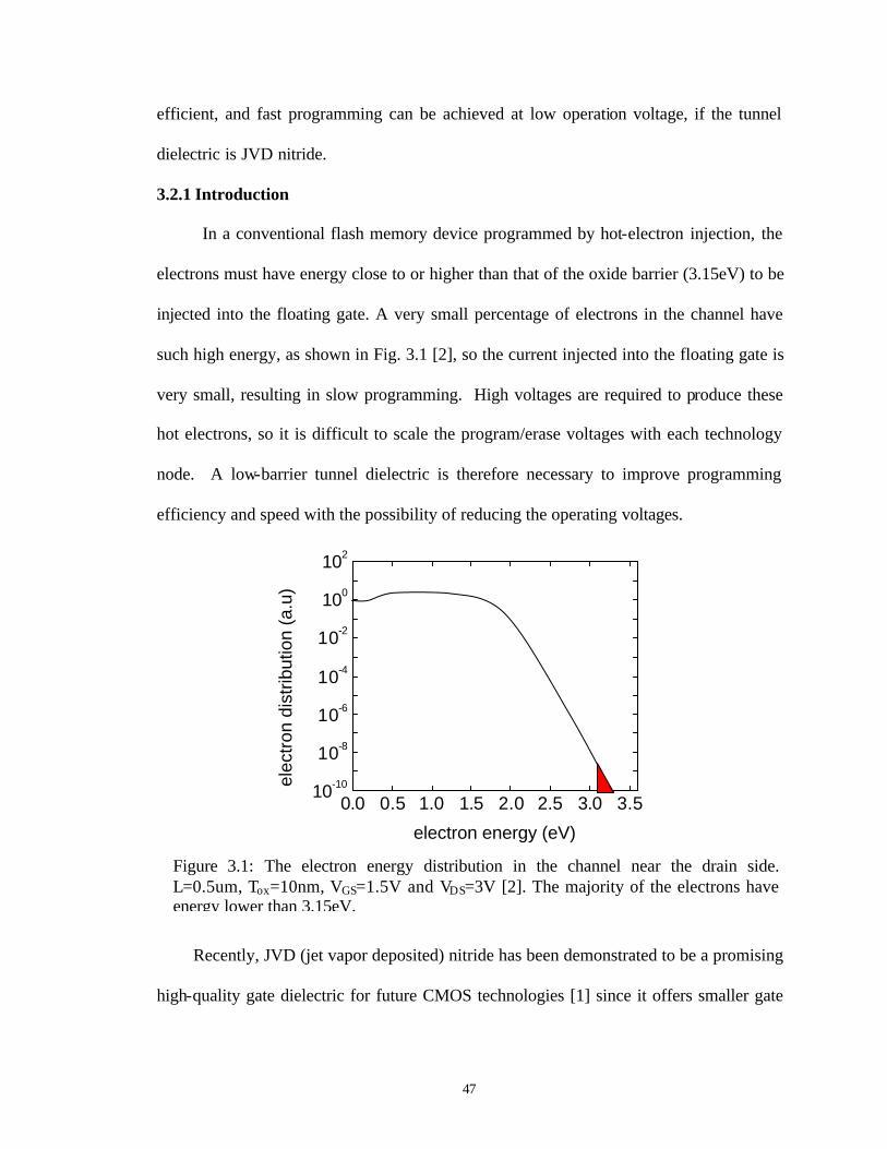


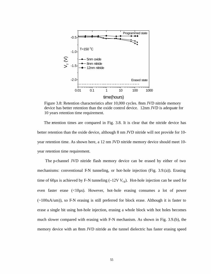
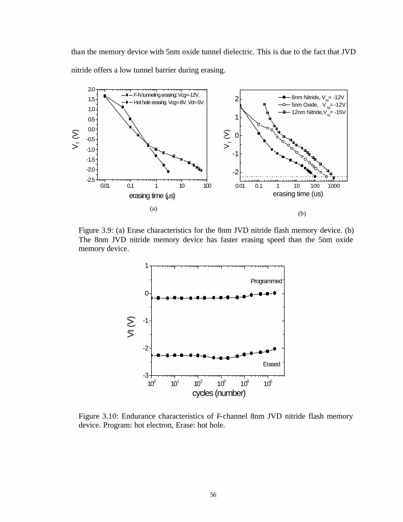
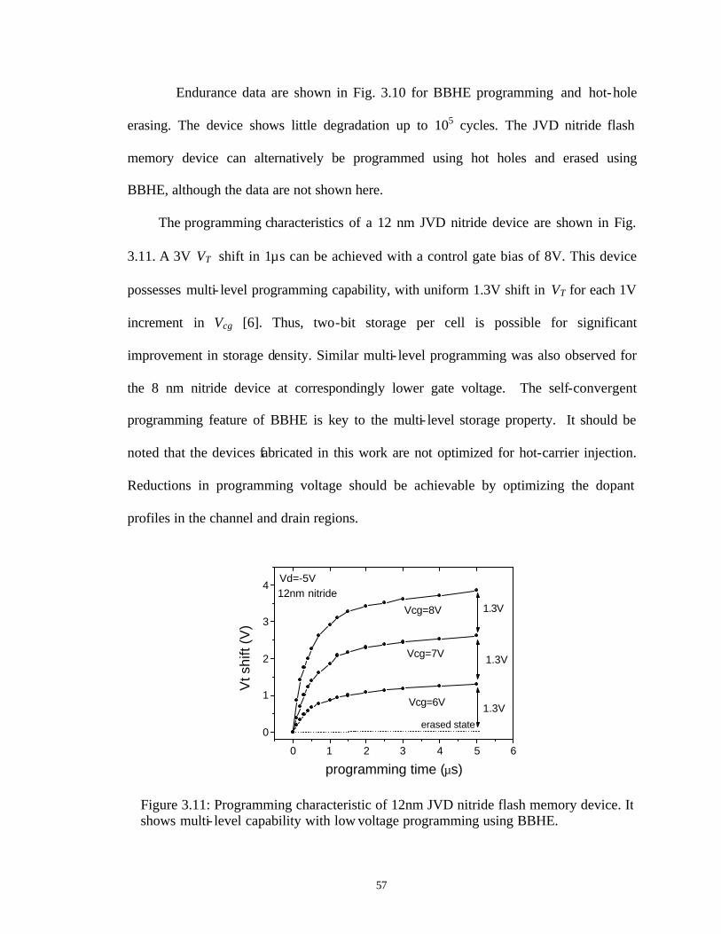


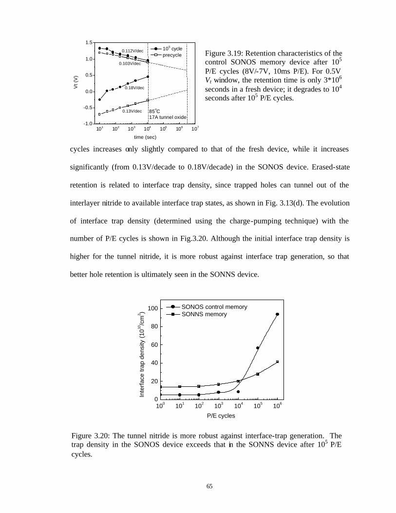


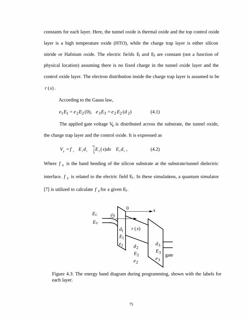


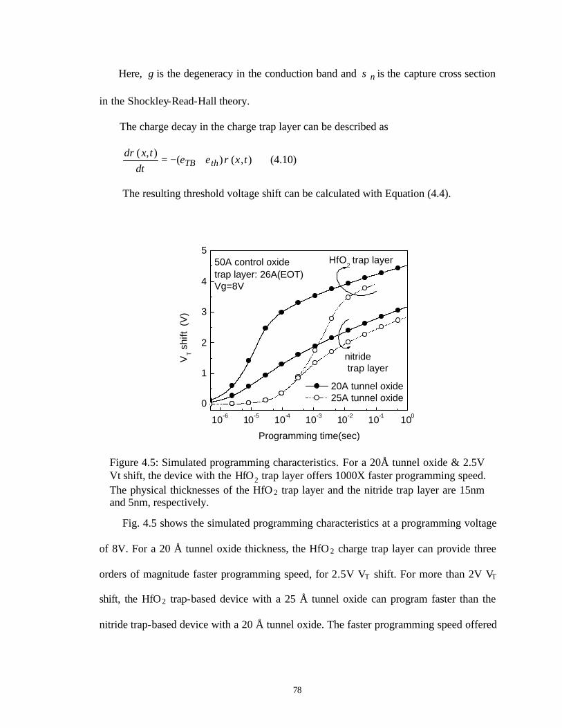

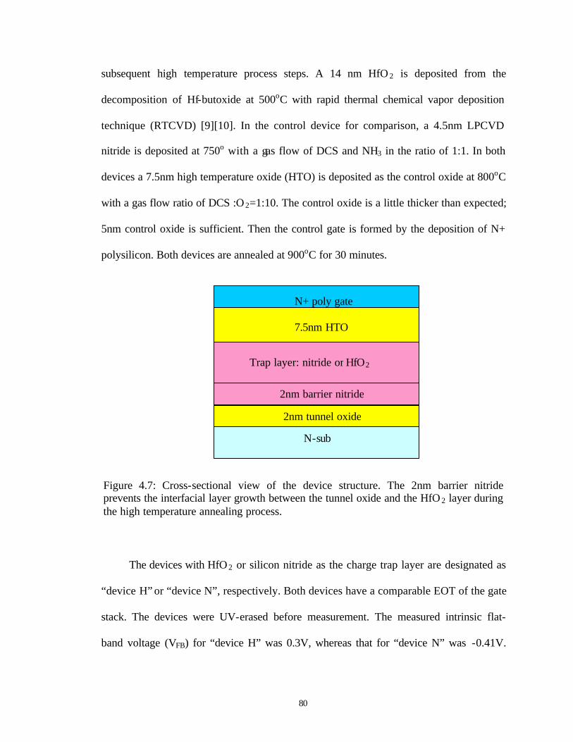


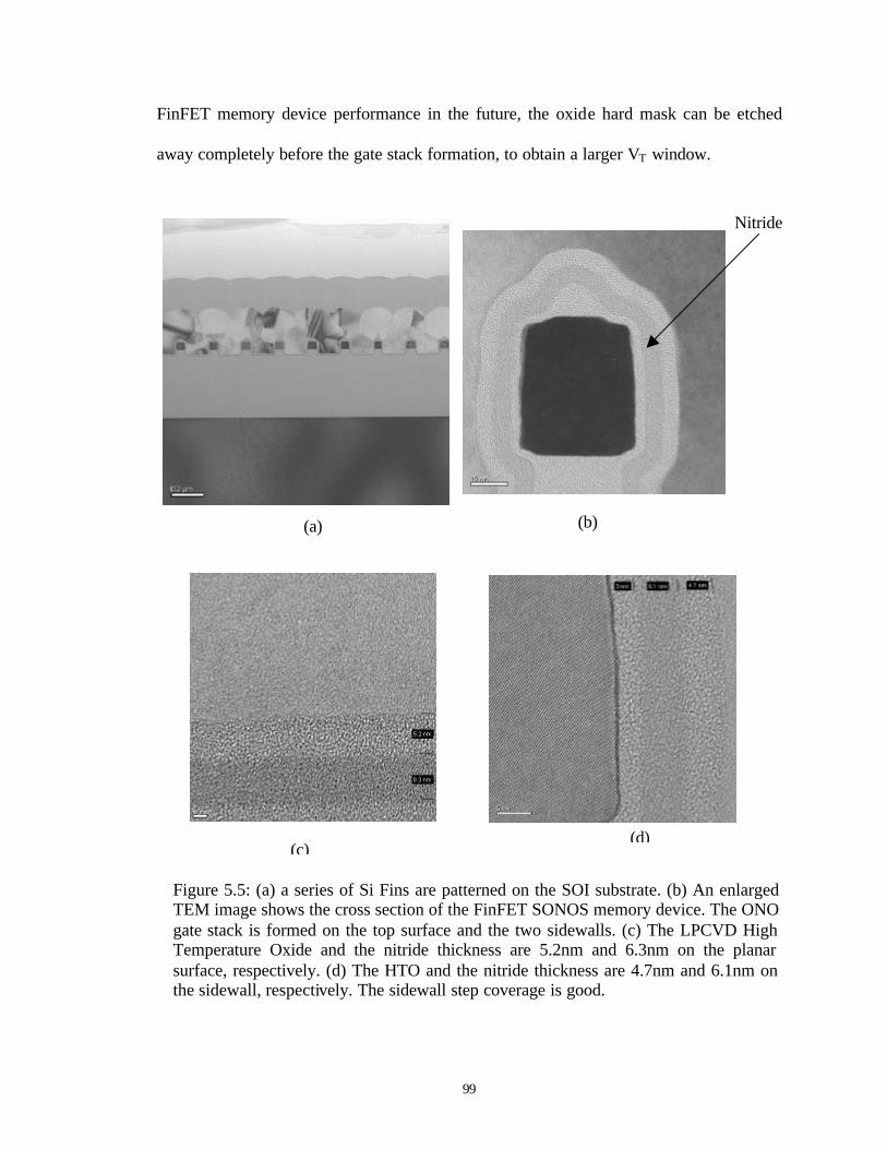


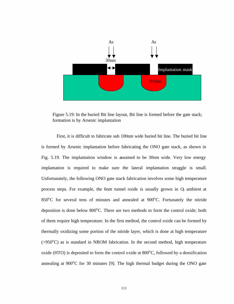


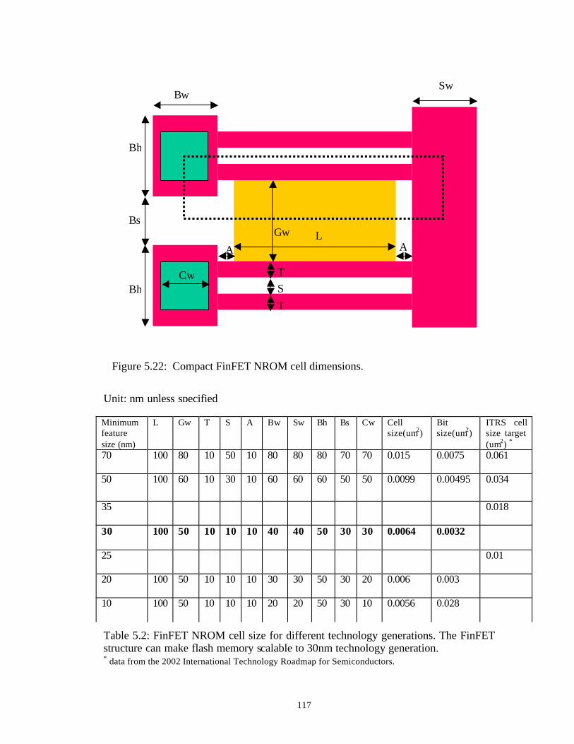


![Emerging Challenges in NAND Flash Technology FG NAND cell has been scaled down over 18 years. [ Year ] MLC SLC? 9 Presentation Agenda NAND Flash Market Overview Technology Scaling](https://static.documents.pub/doc/80x56/5ad528727f8b9a075a8c8fef/emerging-challenges-in-nand-flash-technology-fg-nand-cell-has-been-scaled-down-over.jpg)


