+ Models
CERI-2837; No of Pages 7
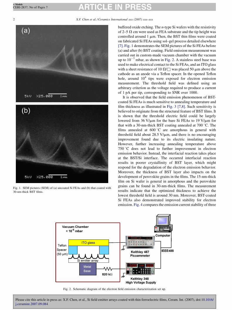
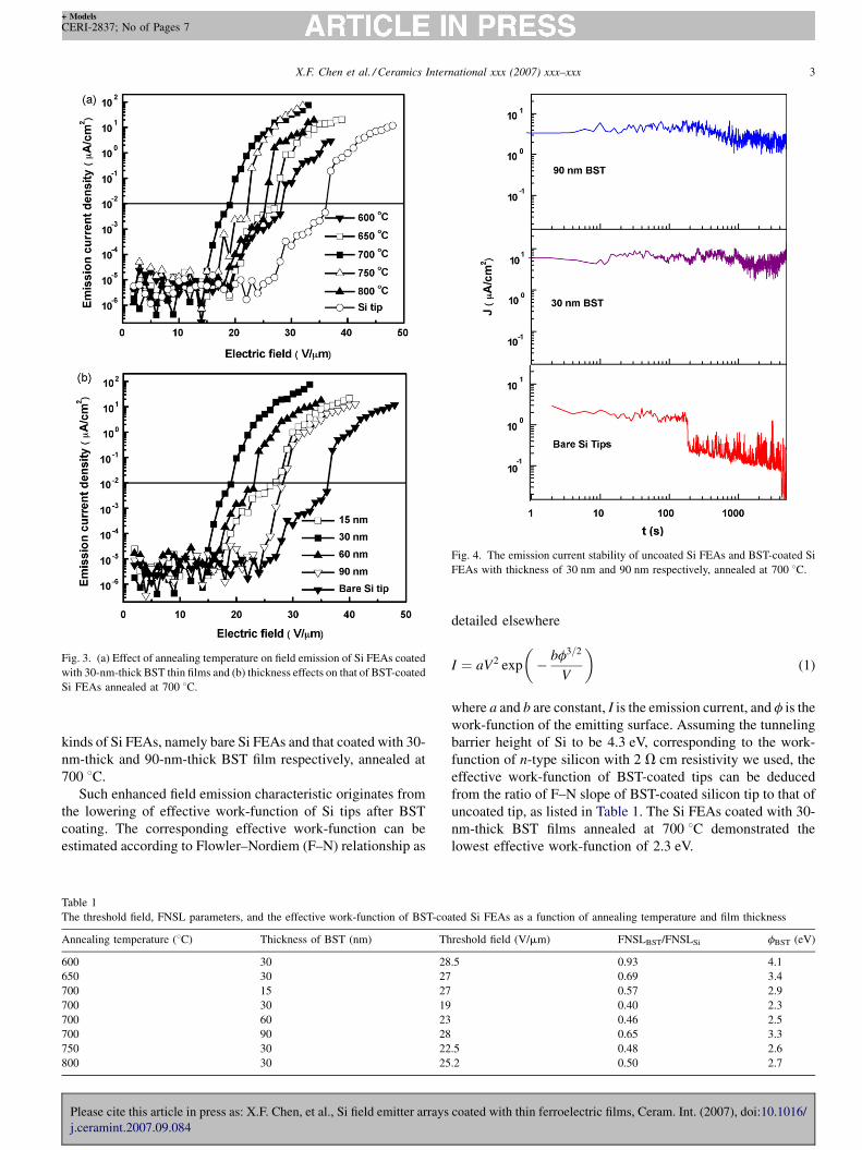
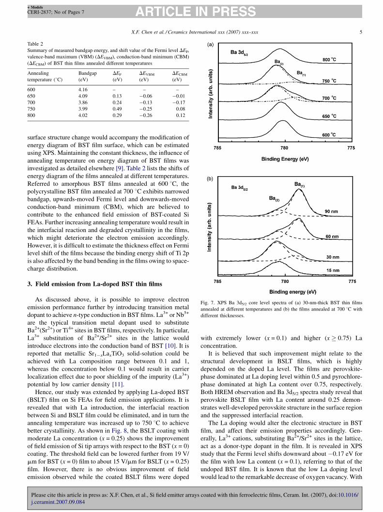
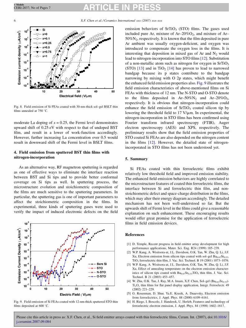
Si field emitter arrays coated with thin ferroelectric films
X.F. Chen a,*, W. Zhu b, H. Lu b, J.S. Pan c, H.J. Bian b, O.K. Tan b, C.Q. Sun b
a Electronic Materials Research Laboratory, Key Laboratory of the Ministry of Education, Xi’an Jiaotong University, Xi’an 710049, Chinab Microelectronics Centre, School of Electrical and Electronic Engineering, Nanyang Technological University, Nanyang Avenue, Singapore 639798
c Institute of Materials Research & Engineering, 3 Research Link, Singapore 117602
Abstract
This paper demonstrates novel approach on Si field emitter arrays (FEAs) coated with thin ferroelectric films for vacuum microelectronic
applications, which exhibit enhanced electron emission behaviors. The films were deposited using sol–gel and sputtering process, respectively. In
sol–gel approach, the emission behavior is highly correlated to the crystallinity of (Ba,Sr)TiO3 (BST) layer. The interfacial reaction between Si and
BST film would deteriorate the crystallinity of the films, and in turn impede the electron emission from silicon tips. The film thickness and the
dopants also affect the emission behaviors significantly. In sputtering process, the nitrogen-incorporated SrTiO3 (STO) films are deposited with
eliminated interfacial due to relatively lower processing temperature. The enhanced emission characteristics are highly correlated with nitrogen-
incorporation and film thickness. These encouraging results have offered great promise for the application of ferroelectric films in field emission
devices.
# 2007 Elsevier Ltd and Techna Group S.r.l. All rights reserved.
Keywords: Field emission; Ferroelectric thin films
www.elsevier.com/locate/ceramint
Available online at www.sciencedirect.com
Ceramics International xxx (2007) xxx–xxx
1. Introduction
Field emission (FE) is usually based on the physical
phenomenon of quantum tunneling, in which electrons are
injected from the surface of materials into vacuum under the
applied electric field. Compared to thermionic cathode vacuum
tubes, the field emission devices could offer some unique
advantages, such as compact size, modest power consumption
and possibility to integrate with solid-state electronics. They
have a number of important applications both in military and
domestic industries, including flat panel displays, microcol-
umns for electron beam parallel writing, various types of
vacuum microelectronic devices, RF devices, vacuum sensors
and space instruments [1]. To date, a variety of field emission
cold cathode materials have been developed, including
materials for microfabricated field emitter arrays, diamond
and related films, quasi one-dimensional nanomaterials like
carbon nanotubes and ferroelectric materials. Recently, the
enhanced electron emission behavior from the Ba0.66Sr0.33TiO3
(BST)-coated silicon tip arrays was discovered by Kang [2,3]
* Corresponding author. Tel.: +86 29 82668584; fax: +86 29 82668794.
E-mail address: [email protected] (X.F. Chen).
0272-8842/$32.00 # 2007 Elsevier Ltd and Techna Group S.r.l. All rights reserve
doi:10.1016/j.ceramint.2007.09.084
Please cite this article in press as: X.F. Chen, et al., Si field emitter arrays
j.ceramint.2007.09.084
and Zhu [4]. BST is a well-known material in ferroelectric
family. However, the emission current from BST film surface is
different from the so-called ferroelectric electron emission
(FEE). It is known that FEE is an unconventional electron
emission effect [5,6] and generated by a deviation of
spontaneous polarization from the equilibrium state under
pyroelectric, piezoelectric effects, or polarization reversal. In
contrast, the emission current from BST thin films demon-
strates a steady state current and is much similar to the classic
types of electron emission from the solids. The emission
behavior is found to be highly correlated with their structure
[2,3] and stoichiometric composition [4]. In this paper, we
summarize our recent advances on the enhanced field emission
of BST films coated on microfabricated Si field emitter arrays
(FEAs) via sol–gel and sputtering process. Moreover, a series of
structural studies for understanding the corresponding mechan-
ism is given also.
2. Field emission from BST thin films
Firstly, Si FEAs were fabricated using conventional
microfabrication techniques, like photolithographic patterning,
silicon anisotropic etching, oxidation for tip sharpening, and
d.
coated with thin ferroelectric films, Ceram. Int. (2007), doi:10.1016/
Fig. 1. SEM pictures (SEM) of (a) uncoated Si FEAs and (b) that coated with
30-nm-thick BST films.
Fig. 2. Schematic diagram of the electron
X.F. Chen et al. / Ceramics International xxx (2007) xxx–xxx2
+ Models
CERI-2837; No of Pages 7
Please cite this article in press as: X.F. Chen, et al., Si field emitter arrays
j.ceramint.2007.09.084
buffered oxide etching. The n-type Si wafers with the resistivity
of 2–5 V cm were used as FEA substrate and the tip height was
controlled around 1 mm. Then, the BST thin films were coated
on fabricated Si FEAs using sol–gel process detailed elsewhere
[7]. Fig. 1 demonstrates the SEM pictures of the Si FEAs before
(a) and after (b) BST coating. Field emission measurement was
carried out in custom-made vacuum chamber with the vacuum
up to 10�7 mbar, as shown in Fig. 2. A stainless steel base was
used to make electrical contact to the Si FEAs, and an ITO glass
with a sheet resistance of 10 V/& was placed 50 mm above the
cathode as an anode via a Teflon spacer. In the opened Teflon
hole, around 104 tips were exposed for electron emission
measurement. The threshold field was defined using an
arbitrary criterion as the voltage required to produce a current
of 1 pA per tip, corresponding to SNR over 1000.
It is observed that the field emission phenomenon of BST-
coated Si FEAs is much sensitive to annealing temperature and
film thickness as illustrated in Fig. 3 [7,8]. Such sensitivity is
believed to originate from the structural feature of BST films. It
is shown that the threshold electric field could be largely
lowered from 36 V/mm for the bare Si FEAs to 19 V/mm for
that with a 30-nm-thick BST coating annealed at 700 8C. The
films annealed at 600 8C are amorphous in general with
threshold field about 28.5 V/mm, and there is no encouraging
improvement found due to its electric insulating nature.
However, further increasing annealing temperature above
750 8C does not lead to further improvement in electron
emission behavior. Instead, the interfacial reaction takes place
at the BST/Si interface. The occurred interfacial reaction
results in poorer crystallinity of BST layer, which might
respond for the degradation of the electron emission behavior.
Moreover, the thickness of BST layer also impacts on the
development of perovskite grains in the films. The 15-nm-thick
film on Si wafer is general in amorphous and the perovskite
grains can be found in 30-nm-thick films. The measurement
results indicate that the optimized thickness to achieve the
lowest threshold field is around 30 nm. Moreover, BST-coated
Si FEAs also demonstrated improved stability for electron
emission. Fig. 4 compares the emission current stability of three
field emission characterization set up.
coated with thin ferroelectric films, Ceram. Int. (2007), doi:10.1016/
Fig. 3. (a) Effect of annealing temperature on field emission of Si FEAs coated
with 30-nm-thick BST thin films and (b) thickness effects on that of BST-coated
Si FEAs annealed at 700 8C.
Fig. 4. The emission current stability of uncoated Si FEAs and BST-coated Si
FEAs with thickness of 30 nm and 90 nm respectively, annealed at 700 8C.
X.F. Chen et al. / Ceramics International xxx (2007) xxx–xxx 3
+ Models
CERI-2837; No of Pages 7
kinds of Si FEAs, namely bare Si FEAs and that coated with 30-
nm-thick and 90-nm-thick BST film respectively, annealed at
700 8C.
Such enhanced field emission characteristic originates from
the lowering of effective work-function of Si tips after BST
coating. The corresponding effective work-function can be
estimated according to Flowler–Nordiem (F–N) relationship as
Table 1
The threshold field, FNSL parameters, and the effective work-function of BST-coa
Annealing temperature (8C) Thickness of BST (nm) Th
600 30 28
650 30 27
700 15 27
700 30 19
700 60 23
700 90 28
750 30 22
800 30 25
Please cite this article in press as: X.F. Chen, et al., Si field emitter arrays
j.ceramint.2007.09.084
detailed elsewhere
I ¼ aV2 exp
�� bf3=2
V
�(1)
where a and b are constant, I is the emission current, and f is the
work-function of the emitting surface. Assuming the tunneling
barrier height of Si to be 4.3 eV, corresponding to the work-
function of n-type silicon with 2 V cm resistivity we used, the
effective work-function of BST-coated tips can be deduced
from the ratio of F–N slope of BST-coated silicon tip to that of
uncoated tip, as listed in Table 1. The Si FEAs coated with 30-
nm-thick BST films annealed at 700 8C demonstrated the
lowest effective work-function of 2.3 eV.
ted Si FEAs as a function of annealing temperature and film thickness
reshold field (V/mm) FNSLBST/FNSLSi fBST (eV)
.5 0.93 4.1
0.69 3.4
0.57 2.9
0.40 2.3
0.46 2.5
0.65 3.3
.5 0.48 2.6
.2 0.50 2.7
coated with thin ferroelectric films, Ceram. Int. (2007), doi:10.1016/
X.F. Chen et al. / Ceramics International xxx (2007) xxx–xxx4
+ Models
CERI-2837; No of Pages 7
Up to now, the mechanism for such enhanced field emission
behaviors is not well-understood yet. For general under-
standing, the field emission process of BST-coated Si FEAs
would experience three major steps, including supply electrons
to BST film, electron transport to surface, and electron emission
into vacuum. Therefore, some material issues including the
interfacial structure between BST film and Si tip, micro-
structural features in BST film, and energy diagram of emitter
surface would affect electron transport in different steps
accordingly. For examples, the structure development of the
films would be affected by their thickness and annealing
temperature. In high-resolution electron microscopy (HREM)
observation, the 15-nm-thick BST film annealed at 700 8C is
amorphous in general. With thickness increasing, there is a two-
layered structure observed, an amorphous layer near Si wafer
and a polycrystalline layer at the top surface. Fig. 5 illustrates a
typical cross-sectional HREM image of 30-nm-thick BST films
annealed at 700 8C. Moreover, the clear interface contrast can
be observed at BST/Si interface, which is attributed to the
formation of silicon oxide interfacial layer during sol–gel
process. Second ion mass spectroscopy (SIMS) analysis was
also performed to clarify the interface structure. It is shown that
there is a mixture region with Ba, Sr, Ti, Si and O presented at
BST/Si interface. The mixture layer originates from the solid-
state reaction between BSTand Si during the annealing process,
corresponding to (Ba,Sr)TixSiyOz. With annealing temperature
increasing, the reaction is promoted showing the broadened
Fig. 5. Cross-sectional HREM images of sol–gel derived 30-nm-thick BST thin
films annealed at 700 8C.
Fig. 6. SIMS depth profiles for sol–gel BST thin film annealed at (a) 700 8C and
(b) 800 8C for 1 h.
Please cite this article in press as: X.F. Chen, et al., Si field emitter arrays
j.ceramint.2007.09.084
overlapping region of Si, Ba, Sr, Ti and O profiles, as illustrated
in Fig. 6.
Moreover, the surface construction would affect the field
emission behaviors also. X-ray photoelectron spectroscopy
(XPS) study on the Ba 3d5/2 core level spectra of BST films
gives a clear picture on the emitter surface structure [9]. It is
know that the Ba 3d5/2 spectrum is composed of two peaks with
the lower binding energy at 779.1 eV and the high binding
energy at 780.5 eV, corresponding to the coordinated Ba(1) and
uncoordinated Ba(2), respectively. As shown in Fig. 7(a), the
coordinated Ba peak could only be observed in the films
annealed at 700 and 750 8C, indicating the formation of
perovskite grains on the surface. Similarly, only the uncoor-
dinated Ba could be found in 15-nm-thick BST film, indicating
amorphous state at the surface. The coordinated Ba could be
observed in the films with thickness above 30 nm and its
content increase substantially with thickness increasing as
shown in Fig. 7(b).
In perovskite structure, the corner-shared TiO6 octahedra
dominate the main electronic properties of BST. In a simplified
ionic model, it would lead to a completely full O 2p valence
band and an empty Ti 3d conduction band for BST. Therefore,
coated with thin ferroelectric films, Ceram. Int. (2007), doi:10.1016/
Fig. 7. XPS Ba 3d5/2 core level spectra of (a) 30-nm-thick BST thin films
annealed at different temperatures and (b) the films annealed at 700 8C with
different thicknesses.
Table 2
Summary of measured bandgap energy, and shift value of the Fermi level DEF,
valence-band maximum (VBM) (DEVBM), conduction-band minimum (CBM)
(DECBM) of BST thin films annealed different temperatures
Annealing
temperature (8C)
Bandgap
(eV)
DEF
(eV)
DEVBM
(eV)
DECBM
(eV)
600 4.16 – – –
650 4.09 0.13 �0.06 �0.01
700 3.86 0.24 �0.13 �0.17
750 3.99 0.49 �0.25 0.08
800 4.02 0.29 �0.26 0.12
X.F. Chen et al. / Ceramics International xxx (2007) xxx–xxx 5
+ Models
CERI-2837; No of Pages 7
surface structure change would accompany the modification of
energy diagram of BST film surface, which can be estimated
using XPS. Maintaining the constant thickness, the influence of
annealing temperature on energy diagram of BST films was
investigated as detailed elsewhere [9]. Table 2 lists the shifts of
energy diagram of the films annealed at different temperatures.
Referred to amorphous BST films annealed at 600 8C, the
polycrystalline BST film annealed at 700 8C exhibits narrowed
bandgap, upwards-moved Fermi level and downwards-moved
conduction-band minimum (CBM), which are believed to
contribute to the enhanced field emission of BST-coated Si
FEAs. Further increasing annealing temperature would result in
the interfacial reaction and degraded crystallinity in the films,
which might deteriorate the electron emission accordingly.
However, it is difficult to estimate the thickness effect on Fermi
level shift of the films because the binding energy shift of Ti 2p
is also affected by the band bending in the films owing to space-
charge distribution.
3. Field emission from La-doped BST thin films
As discussed above, it is possible to improve electron
emission performance further by introducing transition metal
dopant to achieve n-type conduction in BST films. La3+ or Nb5+
are the typical transition metal dopant used to substitute
Ba2+(Sr2+) or Ti4+ sites in BST films, respectively. In particular,
La3+ substitution of Ba2+/Sr2+ sites in the lattice would
introduce electrons into the conduction band of BST [10]. It is
reported that metallic Sr1�xLaxTiO3 solid-solution could be
achieved with La composition range between 0.1 and 1,
whereas the concentration below 0.1 would result in carrier
localization effect due to poor shielding of the impurity (La3+)
potential by low carrier density [11].
Hence, our study was extended by applying La-doped BST
(BSLT) film on Si FEAs for field emission applications. It is
revealed that with La introduction, the interfacial reaction
between Si and BSLT film could be eliminated, and in turn the
annealing temperature was increased up to 750 8C to achieve
better crystallinity. As shown in Fig. 8, the BSLT coating with
moderate La concentration (x = 0.25) shows the improvement
of field emission of Si tip arrays with respect to the BST (x = 0)
coating. The threshold field can be lowered further from 19 V/
mm for BST (x = 0) film to about 15 V/mm for BSLT (x = 0.25)
film. However, there is no obvious improvement of field
emission observed while the coated BSLT films were doped
Please cite this article in press as: X.F. Chen, et al., Si field emitter arrays
j.ceramint.2007.09.084
with extremely lower (x = 0.1) and higher (x � 0.75) La
concentration.
It is believed that such improvement might relate to the
structural development in BSLT films, which is highly
depended on the doped La level. The films are perovskite-
phase dominated at La doping level within 0.5 and pyrochlore-
phase dominated at high La content over 0.75, respectively.
Both HREM observation and Ba 3d5/2 spectra study reveal that
perovskite BSLT film with La content around 0.25 demon-
strates well-developed perovskite structure in the surface region
and the suppressed interfacial reaction.
The La doping would alter the electronic structure in BST
film, and affect their emission properties accordingly. Gen-
erally, La3+ cations, substituting Ba2+/Sr2+ sites in the lattice,
act as a donor-type dopant in the film. It is revealed in XPS
study that the Fermi level shifts downward about �0.17 eV for
the film with low La content (x = 0.1), referring to that of the
undoped BST film. It is known that the low La doping level
would lead to the remarkable decrease of oxygen vacancy. With
coated with thin ferroelectric films, Ceram. Int. (2007), doi:10.1016/
Fig. 8. Field emission of Si FEAs coated with 30-nm-thick sol–gel BSLT thin
films annealed at 750 8C.
X.F. Chen et al. / Ceramics International xxx (2007) xxx–xxx6
+ Models
CERI-2837; No of Pages 7
moderate La doping of x = 0.25, the Fermi level demonstrates
upward shift of 0.25 eV with respect to that of undoped BST
film, and result in a lower of work-function accordingly.
However, further increasing La concentration over 0.5 would
result in downward shift of the Fermi level in BSLT films.
4. Field emission from sputtered BST thin films with
nitrogen-incorporation
As an alternative way, RF magnetron sputtering is regarded
as one of effective ways to eliminate the interface reaction
between BST and Si tips and to provide better conformal
coverage on Si tips as well. In sputtering process, the
microstructure evolution and stoichiometric composition of
the films are much sensitive to the sputtering parameters. In
particular, the sputtering gas is one of important parameters to
affect the stoichiometric composition in the films. In
experimental, three kinds of sputtering gases were used to
verify the impact of induced electronic defects on the field
Fig. 9. Field emission of Si FEAs coated with 12-nm-thick sputtered STO thin
films deposited at 600 8C.
Please cite this article in press as: X.F. Chen, et al., Si field emitter arrays
j.ceramint.2007.09.084
emission behaviors of SrTiO3 (STO) films. The gases used
included pure Ar, mixture of Ar–20%O2, and mixture of Ar–
50%N2, respectively. It is known that the film deposited in pure
Ar ambient was usually oxygen-deficient, and oxygen was
introduced to compensate the oxygen loss in the films. It is
interesting that deposition in mixed gas of Ar and N2 would
lead to nitrogen-incorporation into STO films [12]. Substitution
of a non-metallic atom such as nitrogen for oxygen in SrTiO3
(STO) [13] and in TiO2 [14] has proven to lead to narrowed
bandgap because its p states contribute to the bandgap
narrowing by mixing with O 2p states, which might benefit
the enhanced field emission properties also. Fig. 9 illustrates the
field emission characteristics of above-mentioned films on Si
FEAs with thickness of 12 nm. The N-STO and O-STO denote
to the films deposited in Ar–50%N2 and Ar–20%O2,
respectively. It is obvious that nitrogen-incorporation could
enhance the field emission of SrTiO3 coated silicon tip by
lowering the threshold field to 17 V/mm. In experimental, the
nitrogen-incorporation in STO films has been confirmed using
Fourier transform infrared spectroscopy (FTIR), Auger
electron spectroscopy (AES) and XPS, respectively. The
preliminary results show that the field emission properties of
STO coated Si FEAs are also depended on the nitrogen content
in the films [12]. However, the detailed state of nitrogen-
incorporated in STO films has not been understood yet.
5. Summary
Si FEAs coated with thin ferroelectric films exhibit
relatively low threshold field and improved emission stability.
The enhanced field emission behaviors are highly correlated to
the microstructure features of coated thin ferroelectric films, the
interface between Si and ferroelectric thin film, and non-
stoichiometric defect and space-charge distribution in the films,
which may alter their energy diagram accordingly. The detailed
mechanism has not been well-understood so far. But the
upwards shift of Fermi level in the films could give a reasonable
explanation on such enhancement. These encouraging results
would offer great promise for the application of ferroelectric
films in field emission devices.
References
[1] D. Temple, Recent progress in field emitter array development for high
performance applications, Mater. Sci. Eng. R24 (1999) 185–239.
[2] W.P. Kang, A. Wisitsora-at, J.L. Davidson, O.K. Tan, W. Zhu, Q. Li, J.F.
Xu, Electron emission from silicon tips coated with sol–gel Ba0.67Sr0.33-
TiO3 ferroelectric thin film, J. Vac. Sci. Technol. B 19 (2001) 1073–1076.
[3] W.P. Kang, A. Wisitsora-at, J.L. Davidson, O.K. Tan, W. Zhu, Q. Li, J.F.
Xu, Effect of annealing temperature on the electron emission character-
istics of silicon tips coated with Ba0.67Sr0.33TiO3 thin film, J. Vac. Sci.
Technol. B 21 (2003) 453–457.
[4] W. Zhu, O.K. Tan, J. Ray, M.A. Imam, X.F. Chen, Sol–gel (Ba0.67Sr0.33)-
TixOy thin films for flat panel display application, Integr. Ferroelectr. 49
(2002) 221–229.
[5] G. Rosenman, D. Shur, Ya.E. Krasik, A. Duaevsky, Electron emission
from ferroelectrics, J. Appl. Phys. 88 (2000) 6109–6161.
[6] H. Riege, I. Boscolo, J. Handerek, U. Herleb, Features and technology of
ferroelectric electron emission, J. Appl. Phys. 84 (1998) 1602–1617.
coated with thin ferroelectric films, Ceram. Int. (2007), doi:10.1016/
X.F. Chen et al. / Ceramics International xxx (2007) xxx–xxx 7
+ Models
CERI-2837; No of Pages 7
[7] X.F. Chen, H. Lu, W.G. Zhu, O.K. Tan, Enhanced field emission of silicon
tips coated with sol–gel-derived (Ba0.65Sr0.35)TiO3 thin film, Surf. Coat.
Technol. 198 (2005) 266–269.
[8] H. Lu, X.F. Chen, W.G. Zhu, J.S. Pan, O.K. Tan, Annealing temperature
effect on field emission of silicon emitter arrays with sol–gel
(Ba0.65Sr0.35)TiO3 coatings, Ferroelectrics 334 (2006) 529–537.
[9] H. Lu, J.S. Pan, X.F. Chen, W.G. Zhu, O.K. Tan, Influence of annealing
temperature on the band structure of sol–gel Ba0.65Sr0.35TiO3 thin films on
n-type Si(1 0 0), Appl. Phys. Lett. 88 (2006) 132907.
[10] X.G. Guo, X.S. Chen, Y.L. Sun, L.S. Sun, X.H. Zhou, W. Lu, Electronic
band structure of Nb doped SrTiO3 from first principle calculation, Phys.
Lett. A 317 (2003) 501–506.
Please cite this article in press as: X.F. Chen, et al., Si field emitter arrays
j.ceramint.2007.09.084
[11] Y. Tokura, Y. Taguchi, Y. Okada, Y. Fujishima, T. Arima, Filling depen-
dence of electronic properties on the verge of metal-mott-insulator
transition in Sr1�xLaxTiO3, Phys. Rev. Lett. 70 (1993) 2126–2129.
[12] X.F. Chen, H. Lu, H.J. Bian, W.G. Zhu, C.Q. Sun, O.K. Tan, Electron
emission of silicon field emitter arrays coated with N-doped SrTiO3 film,
J. Electroceram. 16 (2006) 419–423.
[13] J. Wang, S. Yin, M. Komatsu, Q. Zhang, F. Saito, T. Sato, Preparation and
characterization of nitrogen doped SrTiO3 photocatalyst, Appl. Catal. B:
Environ. 52 (2004) 149–156.
[14] R. Asahi, T. Morikawa, T. Ohwaki, K. Aoki, Y. Taga, Visible-light
photocatalysis in nitrogen-doped titanium oxides, Science 293 (2001)
269–271.
coated with thin ferroelectric films, Ceram. Int. (2007), doi:10.1016/