IEEE TRANSACTIONS ON ELECTRON DEVICES, VOL. 55, NO. 11, NOVEMBER 2008 3107
Si, SiGe Nanowire Devices by Top–DownTechnology and Their Applications
Navab Singh, Kavitha D. Buddharaju, S. K. Manhas, A. Agarwal, Subhash C. Rustagi,G. Q. Lo, N. Balasubramanian, and Dim-Lee Kwong
Invited Paper
Abstract—Nanowire (NW) devices, particularly the gate-all-around (GAA) CMOS architecture, have emerged as the front-runner for pushing CMOS scaling beyond the roadmap. Thesedevices offer unique advantages over their planar counterpartswhich make them feasible as an option for 22-nm and beyond tech-nology nodes. This paper reviews the current technology status forrealizing the GAA NW device structures and their applications inlogic circuit and nonvolatile memories. We also take a glimpse intoapplications of NWs in the “more-than-Moore” regime and brieflydiscuss the application of NWs as biochemical sensors. Finally, wesummarize the status and outline the challenges and opportunitiesof the NW technology.
F EATURE-SIZE scaling in CMOS technology has contin-ued to follow the diktat of Moore’s law [1] for more than
40 years. Although the structure remained planar, the CMOSdevice architecture has undergone many a mutation to sustainthe scaling pace. Implementation of LDD, lateral nonunifor-mity in channel doping, reduction in junction depth, and verticalnonuniformity in well doping including pocket and HALOimplants are a few examples. In addition, the performanceof scaled devices has been further improved by introducingstressors in the structure to improve mobility [2], [3]. Thegate leakage current issue is tackled by the following ways:1) slowing down the scaling of the gate oxide thickness and2) introducing high-k materials in the gate dielectric [4]. Cir-cuits of 45 nm with high-k and metal gates are in production [5].
The device scaling, however, appears to be reaching the end-of-the-technology roadmap [6]. The major challenges beingfaced in further scaling are as follows: 1) degraded gate electro-
Manuscript received May 2, 2008; revised July 28, 2008. Current versionpublished October 30, 2008. The review of this paper was arranged by EditorC. Guy.
N. Singh, K. D. Buddharaju, A. Agarwal, S. C. Rustagi, G. Q. Lo, andD.-L. Kwong are with the Institute of Microelectronics, Singapore 117685(e-mail: [email protected]).
S. K. Manhas is with the Department of Electronics and Computer Engineer-ing, Indian Institute of Technology, Roorkee 247667, India.
N. Balasubramanian is with Silterra, Kulim 09000, Malaysia.Color versions of one or more of the figures in this paper are available online
at http://ieeexplore.ieee.org.Digital Object Identifier 10.1109/TED.2008.2005154
Fig. 1. Progression of device structure from single-gated planar to fully GAANW MOSFETs.
static control of the channel potential leading to short-channeleffects—threshold voltage roll-off, large DIBL, and poor sub-threshold slope (SS); 2) increased gate and junction leakages;3) reduced channel mobility; and 4) increased source/drain (S/D)resistance. The increased doping in the channel which is neededto help the control of the gate over the channel vis-à-vis that ofsource and drain terminals leads to degraded performance.
The electrostatics gets improved in multiple-gate structures[7] as the gate influences the channel potential from more thanone side and thus relaxes the demand on the doping. Fig. 1shows the evolution of multiple-gate transistors schematicallyin the order of increasing gate electrostatic control. Apparently,the gate-all-around (GAA) structure is the most resistant toshort-channel effects among all the emerging device structuresfor a given silicon body thickness. The simulations [8] indicate
3108 IEEE TRANSACTIONS ON ELECTRON DEVICES, VOL. 55, NO. 11, NOVEMBER 2008
that in cylindrical GAA architecture, the gate length can bescaled to 5 nm with the corresponding scaling of the intrinsicnanowire (NW) channel body. Furthermore, the cylindricalgeometry gives inverse logarithmic dependence of the gatecapacitance on the channel diameter, and thus, the gate length inthese devices can be scaled with wire diameter without reducingthe gate dielectric thickness. It also makes the GAA NWarchitecture an excellent candidate for SONOS-type nonvolatilememory (NVM) applications where the gate dielectric has to benecessarily thicker.
Interestingly, the NW structures provide for very largesurface-to-volume ratio that makes them ideal structures forsensing of chemical/biochemical species [9]. The NW surfacecan be sensitized to bind [10] the target species which has amagnified impact on the electrical transport in the body of theNW due to its smaller volume.
The fabrication technology of NW channels can be broadlycategorized into two groups, namely, 1) the bottom–up ap-proach and 2) the top–down approach. In the case of bottom–upapproach, the wire channels are synthesized, for example, usingvapor–liquid–solid chemistry [11], typically with the help of ametal catalyst. Many approaches have been investigated for as-sembly [12]–[14], including the templated growth [15] of NWs.Fabrication of silicon NWs (Si-NWs) and devices has also beenreported using etching, with the platinum NW masks beingprepared with the help of the superlattice NW pattern transfer(SNAP) process [16], [17]. NWs have also been synthesizedin the “microcracks” induced in the thin films using stress fortemplated growth [18].
The bottom–up approaches involving synthesis of NWs havebeen extensively reviewed in the literature, for instance, byXia et al. [11], Law et al. [19], and Lu and Lieber [20], andare not discussed in further detail in this paper. In the top–downapproach, the NWs are prepared in place utilizing lithographyand etch processes, followed by trimming or stress-limitedoxidation techniques. Integration of top–down-fabricated NWsin circuit functionality is straightforward, while the bottom–upapproach faces a daunting challenge of assembling the wiresinto circuit functions.
This paper reviews the current status of the NW technologyand applications, with a particular focus on the top–downapproach and the GAA NW CMOS device architecture. Thetop–down fabrication approaches proposed by different groupsare reviewed in Section II. The device electrical characteriza-tion and carrier transport results are reviewed in Section III.Recently reported circuit implementations using these novel de-vices are discussed in Section IV. The application of the GAANW architecture as NVM is discussed in Section V. Section VIbriefly reports the results for different sensor applications ofthe NW-based devices. The challenges and opportunities of theNW technology are discussed in Section VII, and conclusionsare summarized in Section VIII.
II. NW AND GAA NW DEVICE FABRICATION
There are a few variants of fabrication approaches reportedfor the realization of NWs and devices using the top–downtechnique. All approaches start with the silicon wafers as the
substrate and involve lithography and etching processes forstarting pattern definition. Different process steps such as hard-mask trimming [21], etching in H2 ambient [22], and/or stress-limited oxidation processes [23] follow to convert the siliconstructures defined in the earlier step into NWs. The stress-limited oxidation is usually carried out at low temperature tokeep the grown oxide in stress to progressively slow downthe oxidation rate, thus leaving a nanometer-scale silicon coreembedded in the oxide. The stress-limited oxidation was firstreported on vertical 1-D nanorod structures by Liu et al. [23]wherein the silicon columns of about 40–50 nm in diameter andabout 1000 nm in height were subjected to long oxidation (upto more than 40 h) at low temperatures (800 ◦C) that reducedthe core of the silicon to less than 5 nm.
Kedzierski et al. [24] made use of this stress-limited oxida-tion for obtaining the lateral NWs and utilized those as transis-tor channels, with the thick stress-limited grown oxide servingas the gate dielectric. Although the gate dielectric thickness waslarge (∼25 nm), the devices showed good performance in termsof on-current, on-to-off-current ratios, DIBL, as well as SS.
As an alternative approach for reducing the fins to NWs,hydrogen annealing of an ultranarrow fin has been used byYang et al. [25]. NWs with 10-nm diameter and truncated cylin-drical shape have been fabricated. The fabricated sub-10-nm-gate-length NW FETs in omega gate architecture showed verylow OFF-state leakage current and excellent gate delay. Hy-drogen annealing has also been reported by Ernst et al. [26]with vertically stacked NW for high-performance circuits.Tezuka et al. [22] have applied hydrogen annealing/etching forSi and SiGe NWs to reduce the sidewall roughness.
Another approach to define Si-NWs and GAA transistors hasbeen reported by Suk et al. [21] and Yeo et al. [27]. In this ap-proach, silicon fin is split into two NWs—twin Si-NW—usingthe hard-mask trimming process. The lateral dimensions ofNWs are defined by trimming of the hard mask, while thevertical dimensions are given by the thickness of the siliconepitaxial layer on top of a sacrificial SiGe layer. The GAAtransistors fabricated on these 8-nm-thick wires with grownoxide as the gate dielectric and damascene poly-silicon gateelectrodes down to the physical gate length of 15 nm showexcellent gate control and other characteristics.
Our group at IME, Singapore, has extensively implementedthe self-limiting oxidation process for Si-NW fabrication inlateral as well as vertical architectures. The wires have beencarefully released by etching away the grown oxide in dilute HF[28], [29]. Fig. 2 shows the SEM images of various combina-tions of NWs fabricated using the lithographic pattern transferand self-limiting oxidation processes. The different NW shapesand arrangements are a result of variants defined on the mask.
Fig. 2(a) shows a 0.85-μm-long single NW obtained froma low-aspect-ratio fin. Fig. 2(b) shows vertically aligned twinNWs fabricated out of a single high-aspect-ratio fin, with thetop-left inset showing the TEM image of a partially oxidizedfin and the bottom-right inset showing the same for verticallyaligned twin Si-NWs after full conversion. Fin aspect ratios ofabout two and more result in twin wires. Fig. 2(c) shows a 1-Darray of NWs. The large-area ordered mesh of NWs shownin Fig. 2(d) is an indication of the robustness of the process.
SINGH et al.: Si, SiGe NANOWIRE DEVICES BY TOP–DOWN TECHNOLOGY AND THEIR APPLICATIONS 3109
Fig. 2. (a) Single Si-NW. (b) Vertically stacked twin Si-NWs. The top insetshows the TEM cross section of a partially oxidized silicon fin indicating themechanism; the center region is oxidizing faster and has become much thinnerthan the top and the bottom. The lower inset shows the TEM cross section ofthe twin NW embedded in oxide. (c) Array of Si-NWs. (d) Large-area regularmesh of NWs. The inset shows the curved NWs by the curved pattern definedusing lithography. (e) and (f) 1.0-μm tall isolated and dense arrays of verticalSi-NWs of ∼20-nm diameter, respectively.
The inset on the top-left corner shows the curved NWs obtainedupon oxidation of curved silicon fins defined by lithography ona bulk wafer. Fig. 2(e) and (f) shows the SEM micrograph ofisolated and dense array of vertical NWs fabricated using thesame process sequence as lateral NWs.
By utilizing such NWs as channel body, we have fabri-cated GAA NW-FETs [28], NW-Schottky barrier FETs [30],SONOS-type NVM cells [31], and NW logic circuits. In ourapproach, the device and circuit fabrication is straightforward—very similar to the process steps used in standard CMOS flow.The gate oxide is grown or deposited on the NWs, followedby gate electrode deposition and definition. S/D implantation,metallization, followed by alloying complete the fabricationprocess similar to the planar FETs. The NW channel remainsundoped, i.e., no intentional doping to adjust VTH or to controlshort-channel effects is introduced. After NW formation, thekey process is gate definition in which the dry etching processrequires a high selectivity to gate dielectric.
Shown in Fig. 3(a) is the tilted view of the SEM imageafter gate definition. The TEM cross section across the NWchannel is shown in Fig. 3(b), where ∼3-nm-thick Si-NW and
Fig. 3. (a) GAA NW transistor with gate length of 350 nm after gate pattern-ing and (b) its TEM cross section in which ∼3-nm-thick Si-NW surrounded by4-nm SiO2 followed by poly-silicon is clearly seen. The inset shows the NWchannel before poly-gate deposition. Reprinted with permission from [29].
Fig. 4. (a) NW device after gate definition. (b) TEM cross-sectional imageof the NW channel across the length. The Ge% is conformed using EDX.Reprinted with permission from [32].
4-nm-thick oxide are clearly seen to be surrounded with theGAA polysilicon. The tilted view of the SEM image of thewire channel just after gate oxidation is shown as an insetin Fig. 3(b).
The top–down fabrication has been extended to SiGe NWchannels targeting high-speed requirements. Pattern-dependentGe condensation (1-D condensation in wider S/D contact padsand 2-D condensation in the narrow fins) is observed during theoxidation process. This leads to heterojunction NW structures(S/D with 30% Ge and NW channel with ∼70% Ge), whichwere integrated into a PFET, with HfO2 as the high-k gatedielectric, along with TaN as the metal gate. Fig. 4(a) showsthe tilted view of the SEM micrograph of the device aftergate definition, along with the TEM cross-sectional image inFig. 4(b) of ∼13-nm-thick NW channel after complete fabri-cation. These Ge-rich NW PFETs in nearly GAA architectureshow significant drive current enhancement vis-à-vis planardevices [32].
One of the issues with the NW-based devices is the low-drive-current capability per NW channel due to ultranarrowchannel body which limits the total number of charge carriers.Increasing the number of NWs laterally helps increase the drivecurrent but at the cost of increased consumption of silicon estateand increase in parasitic. Our group devised a novel approachby vertically stacking the NWs using SiGe as the sacrificiallayer. The differential in oxidation rate between Si and SiGeleads to faster oxidation of SiGe as well as condensation of Geonto the Si surface in the stack [33], [34]. Vertical stacking ofNWs yields much higher drive current without any increase inthe consumption of silicon estate. Fig. 5 shows the SEM images
3110 IEEE TRANSACTIONS ON ELECTRON DEVICES, VOL. 55, NO. 11, NOVEMBER 2008
Fig. 5. Tilted view of the SEM images after release of the stacked NW.(Left) Two stacks of three-stacked NWs. (Right) Five stacks of four-stackedNWs. Reprinted with permission from [34].
Fig. 6. Tilted view of the SEM images of the released Si-NWs of length0.85 μm anchored on both sides (left) before and (right) after high-k and metaldepositions. The wires are severely twisted in the opposite direction after metaldeposition. Reprinted with permission from [35].
of the fabricated 2 × 3 (left) and 5 × 4 (right) stacked arrays ofNW channels. Similar stacking using dry etching of sacrificialSiGe layer, followed by H2, annealing has been reported byErnst et al. [26].
We obtained interesting results related to the impact ofstress on the physical structure of NWs when we fabricatedhigh-k/metal gate GAA devices. Severe twisting of anchoredSi-NW beams was observed once the tantalum nitride (TaN)metal was sputter deposited on the HfO2-coated NWs [35]. TheNWs maintained electrical continuity under estimated stresslevel of the order of ∼4 GPa, which originated from the stressin the deposited metal film. Fig. 6 shows the tilted view SEMimages of the wires before and after metal deposition; severetwisting is clearly visible.
III. ELECTRICAL CHARACTERIZATION OF NW MOSFETs
A. I–V Characteristics
Most of the reported data on the I–V characteristics of GAANW FETs show excellent gate control, near-ideal subthresholdbehavior, high ION/IOFF ratio, and high drive current [21],[27]–[29]. For instance, we obtained ION values of 2.4 and1.3 mA/μm, DIBL values of 8 and 13 mV/V, and SS of 60and 65 mV/dec for NMOS and PMOS, respectively [29]. TheI–V characteristics of these GAA Si-NW devices with 3-nmdiameter are shown in Fig. 7, where the current is normalizedto diameter. Although it is a matter of debate, it is worthmentioning here that the typical trend in the contemporaryNW literature is the normalization to diameter, which may beappropriate only with fully volume-inverted channels existingin the case of ultranarrow undoped wire channels. With thickerwire where conduction remains at surface, it should be more
appropriate to use perimeter for normalization. We have usednormalization to diameter for wire diameters up to 10 nm.Above 10 nm, normalization to perimeter is performed.
The drive performance has been recently improved verysignificantly [36] by appropriate salicidation of S/D extensionsand reduction of gate length to 8 nm; the NMOS drive currentof 3.67 mA/μm is achieved with excellent gate control with10-nm-thick wire channels.
Table I gives the comparative list of device electrical andstructural parameters reported in the literature, along with thebest reported FinFET performance.
The terminal characteristics of heterostructure PFETs(Fig. 6) are shown in Fig. 8. The heterojunction NW FET withNW of ∼13-nm diameter exhibits ∼4.5× transconductanceand drive current improvements compared to the correspondingplanar device. The enhanced hole injection velocity on accountof heterojunction between the source and the channel, com-pressive strain, and high Ge contents (70%) in the channelare speculated as possible contributors to the improvement.Possible causes of low values of absolute current in the case ofboth the NW and the planar device could be not-so-good qualityof interface between HfO2 and SiGe channel body as well as onaccount of increased scattering due to alloyed Ge [32].
In Fig. 9, the transfer characteristics of the GAA NW FETsfabricated on vertically stacked NWs (Fig. 5) are presented. Thedevice electrostatic behavior is as good as reported on singleSi-NW channels in Fig. 7. Thus, our vertical stacking strategyleads to enhanced drive capability per silicon estate withoutcompromising on the other performance parameters. The ab-sence of gm degradation in NMOS relative to that in PMOSpoints to confinement of electrons to the core of the wires andholes to the surface due to bandgap offsets between Si and SiGesketched in the inset of Fig. 9 [34]. The SiGe surface is a resultof Ge condensation into silicon during the oxidation process.
B. Carrier Transport in NW Channels
Characterization and modeling of carrier transport in theNW channels are paramount for applications of these devicesin circuits as well as for physical understanding. The NWdevices are usually undoped, and the short-channel effects arecontrolled using device architecture. The carrier transport in theundoped GAA NW channel is expected to be superior to that ofthe planar bulk FET due to reduced Coulomb scattering—fewerionized dopants in the intentionally undoped NW channel. Dueto the cylindrical symmetry, the surface electric field is higherin GAA FET, and that is expected to reduce the carrier mobility,specifically due to relatively rough surface made up of multipleorientations of the exposed crystal planes. In the case of ul-trathin NW channels, however, most of the carriers remain inthe core of the wire on account of quantum–mechanical effectsand thus enjoy low vertical field and weak scattering. In viewof the aforementioned factors, 1-D transport may have largermean free paths of the carriers and, hence, higher mobility/ballisticity [40]. It will be therefore interesting to investigatethe carrier mobility in NW FETs. However, the measurementof the ultralow capacitance of the NW channels is challenging,and not much data are reported using the measured C–Vcharacteristics.
SINGH et al.: Si, SiGe NANOWIRE DEVICES BY TOP–DOWN TECHNOLOGY AND THEIR APPLICATIONS 3111
Fig. 7. (a) Transfer characteristics of GAA n- and p-FETs (Fig. 3: LG = 350 nm and TOX = 4 nm) showing near-ideal subthreshold swing indicating theexcellent electrostatic control. (b) Drain current characteristics showing that high drive currents are possible in GAA FETs. Reprinted with permission from [29].
TABLE INW AND FinFET TRANSISTOR PERFORMANCE DATA
Fig. 8. (Left) Transconductance gm and (right) output characteristics comparing the SiGe hetero-NW device (Fig. 4: LG = 350 nm, NW diameter of∼13 nm, and THfO2 = 8 nm) performance with that of the planar reference device. The current values are normalized to the perimeter of the wire. Reprintedwith permission from [32].
Cui et al. [41] used the numerically simulated capacitancevalues, in conjunction with the measured I–V characteristics,to estimate the mobility in grown PMOS NW transistors, andestimated the peak hole mobility to be ∼1350 cm2/V · s in10–20-nm-thick Si-NW channels. Tu et al. [42] measured theC–V characteristics for grown Ge NWs with Schottky barrierS/D using special shielding arrangements on the probe stationat low temperatures. The hole mobility value obtained wasreported to be ∼400 cm2/V · s. Recently, Tezuka et al. [22]reported split C–V measurement on top–down omega-gatedstrained and unstrained Si and Ge NW devices by connectingabout 500 device channels in parallel. Mobility enhancementby a factor of 1.6 for holes and 1.9 for electrons is observeddue to the introduced strain. Suk et al. [43] reported a peak
mobility value of 300 cm2/V · s for holes and ∼200 cm2/V · sfor electrons from the C–V measurements of ∼10 000 GAANW device channels in parallel. They reported an enhancementin mobility with reduction in NW diameter until 4 nm and areduction in mobility below 4-nm NW diameter. The highervalues of hole mobility compared to electron mobility wereattributed to the presence of compressive stress in the channeldue to Ge in S/D extension pads. Fig. 10(a) and (b) showsthe mobility data from Tezuka et al. [22] and Suk et al. [43],respectively, plotted against NW diameter/thickness indicatinga large scatter in mobility values and behavior.
The S/D access resistance is another critical parameter whichneeds to be extracted from actual devices and has been an issuein grown NWs due to the small volume of silicon in the contact
3112 IEEE TRANSACTIONS ON ELECTRON DEVICES, VOL. 55, NO. 11, NOVEMBER 2008
Fig. 9. Per-NW Id−Vg and gm−Vg plots for stacked NW n-FETs andp-FETs with LG = 500 nm and NW diameter of ∼30 nm. Reproduced herewith permission from [34].
Fig. 10. Experimentally extracted electron and hole mobility values in NWFETs plotted against the NW diameter/thickness. (a) Is from [22] for the caseof omega-gated NW FET, and (b) is from [43] for the case of GAA NW FET(reprinted with permission).
area. Recently, Suk et al. [22] reported the extension resistancein the range of 1.5–2 kΩ, which is at par with the planar bulkFETs [44].
C. Quantum–Mechanical Effects on Transport atLow Temperature
Electrical characterization of NW devices at cryogenic tem-peratures shows the evidence of discrete energy bands as a re-sult of quantum confinement [45]–[48]. Discrete energy bandsin conduction (valence) band have direct impact on the transportas well as the threshold voltage. Colinge et al. [45], [46] showedoscillatory gm–VG behavior in ultranarrow fin channels. Wehave observed oscillation in ID–VG characteristics and a reduc-tion in drive current at low temperature, possibly on accountof intersubband scattering of the carriers due to large energyseparation in the subbands for NW channels with reduceddiameters (7 nm), as shown in Fig. 11 [48].
IV. NW CMOS CIRCUITS
The NW transistors are being projected for terahertz switch-ing applications due to their good dc performance andextremely small gate-to-channel capacitance resulting in ul-trasmall intrinsic gate delay (CV/I). However, the projecteddelays based on the dc characteristics of individual transistorsand the estimated capacitance using an ideal structure arenot always good indicators of the device performance whileused in circuits due to the presence of various parasitics. The
Fig. 11. Measured IDS−VGS (at VDS = 50 mV) characteristics of ∼7-nmtriangular Si-NW n-FET with effective gate length of ∼300 nm at differenttemperatures: 5 K, 37 K, 77 K, 137 K, 200 K, and 295 K. Reprinted withpermission from [48].
importance of the parasitic associated with the device structurebecomes clearly evident only when the devices are evaluatedin a circuit. For instances, although carbon-nanotube (CNT)devices are projected to be extremely fast devices, the first ringoscillator (RO) reported [49] using CNTs is slow, showing adelay of 1.4 ns due to the parasitic in the fabricated structures.The RO on plastic/glass using grown NW channels from theHarvard group [50] shows a stage delay of ∼14 ns, whichincreases by almost a factor of three on silicon due to increasedparasitic. These devices use larger gate lengths (2 μm). Forevaluating the performance of NW devices in circuits, we havefabricated and characterized the GAA NW CMOS inverterlogic gates and ROs.
A. GAA Si-NW CMOS Inverters
We have demonstrated CMOS inverters with NW GAA chan-nels using the top–down approach [51]–[54]. The symmetryin pull-up/pull-down characteristics has been achieved in twodifferent ways, namely, 1) by using a longer n-channel devicecompared with the p-channel device [51] and 2) by using alarger number of NWs in p-channel transistors [52]–[54]. Inboth ways, the inverters performed with excellent gains, noisemargins, and extremely low (a few nanoamperes) short-circuitcurrent. Fig. 12 shows the tilted view of the SEM image ofNW NMOS and PMOS transistors of the inverter with differentnumber of channels in each device for symmetry. The insetsin the figure show the corresponding wire channels before gatestack deposition.
Shown in Fig. 13(a) are the inverter dc characteristics. Theinverters function well down to 0.2 V of VDD, which is anextremely good result for low-voltage/low-power applications.Fig. 13(b) shows the phase inversion characteristics of GAANW CMOS inverters at 1 MHz. The inverter used for dynamicperformance characterization comprised 20 n-channel and50 p-channel NW MOSFETs.
Wang et al. [17] also reported CMOS NW inverters fabri-cated using the SNAP process. The circuit functionality wasdemonstrated, but the gain was poor. The inverters with grownNWs as the channel bodies and integrated on the glass/plasticsubstrate with long channel [50] show relatively better charac-teristics using high VDD values (∼43 V). This performance may
SINGH et al.: Si, SiGe NANOWIRE DEVICES BY TOP–DOWN TECHNOLOGY AND THEIR APPLICATIONS 3113
Fig. 12. Tilted view of the SEM image of NMOS and PMOS GAA NWtransistors of the inverter logic after poly-gate definition. The channel lengthis 0.35 μm. The NW channels of ∼5–7-nm thickness are shown as insets.
Fig. 13. (a) Transfer characteristics of inverter at different VDD’s, with VIN
and VOUT plotted interchangeably on the x- and y-axes (reprinted withpermission). (b) Dynamic (pulse) response of an inverter with 50 pairs of PMOSchannels and 20 pairs of NMOS channels at 1 MHz. The output levels clearlyreach VDD. LG = 0.35 μm and TOX = 5 nm.
Fig. 14. 41-stage RO waveforms at VDD = 1.2 V. The frequency of oscilla-tion is ∼8.8 MHz, LG = 0.25 μm, and TOX = 9 nm.
have a possible application in stretchable/wearable electronicsfor grown NW device technology once the device structure isimproved to bring down the required VDD values.
B. GAA Si-NW CMOS ROs
ROs are the basic tools to characterize the digital perfor-mance of technology. We have fabricated and characterized41-stage NW CMOS ROs using the top–down approach. Themeasured RO wave shapes are shown in Fig. 14. The waveshapes were picked up with the help of the active probe(Picoprobe model 35 with 50-fF input capacitance). The signalexcursion does not traverse rail to rail due to the smaller size
Fig. 15. (a) SEM image of twin-Si-NW channels after oxide, nitride, andpoly-Si-NC depositions. The inset shows the AFM image of the nanocrystals.(b) TEM cross section of one of the NW channels across the wire length.Reprinted with permission from [61].
of the NW CMOS buffer at the output. The delay per stageis ∼1.4 ns, which is much higher than the best value reported(5.1 ps) using bulk planar FET [55] and 13.9 ps with FinFET[56] devices. Our delay is similar to those reported for CNTRO [49]. The typical delay for planar technology at 0.25-μmgate length, which is incidentally the gate length of the devicesused in our ROs, is ∼40 ps [57]. The main cause of the largerdelay in our case is the low drive current of the NW FETs dueto very narrow channels (vis-à-vis 0.25-μm planar devices) andthe parasitic capacitance due to the relatively long extension ofgate polysilicon beyond the NW channel for gate contact. Thisextension region sits over a thin buried oxide (less than 0.15 μmin thickness) in our structures. We believe that increasingthe buried oxide thickness and implementing the salicidationprocess [36] will significantly improve the RO performance.
V. NW NVMs
Floating-gate NVM has two major limitations that impactthe integration density, namely, 1) neighboring cell interferenceand 2) short-channel effects. Multiple-gate devices in SONOSarchitecture [49] relax these limitations very significantly.The SONOS structure is inherently immune to neighboringcell interference [58], while the multiple-gate structures helpovercome the short-channel effects. Thus, NWs in NVM arepoised to increase the density of integration to ultimate scalinglimit.
In addition, the radial field distribution in cylindrical GAAstructures indicates high concentration of field at the silicon/tunneling oxide interface compared to that in the blockingoxide [31]. In the case of a 5-nm-diameter Si-NW channel, wefind that the cylindrical geometry enhances the electric fieldat the Si–SiO2 interface by approximately three times withrespect to the planar structure with the same dielectric thickness(ONO: 4.5nm/4.5nm/9nm). Also, the GAA device leads tolower electric field in the blocking oxide, i.e., far away fromthe axis of the cylinder. This helps in using Fowler–Nordhiem(F/N) tunneling as the preferred mode of programming anderase.
We fabricated a SONOS-type NVM cell with and withouttrap layer engineering (TLE) using the top–down approach.Fig. 15(a) shows the SEM image of vertically aligned twin-Si-NW channels after tunnel oxide (4.5 nm), trap nitride (4.5 nm),silicon nanocrystals (Si-NCs), and blocking oxide (8 nm)
3114 IEEE TRANSACTIONS ON ELECTRON DEVICES, VOL. 55, NO. 11, NOVEMBER 2008
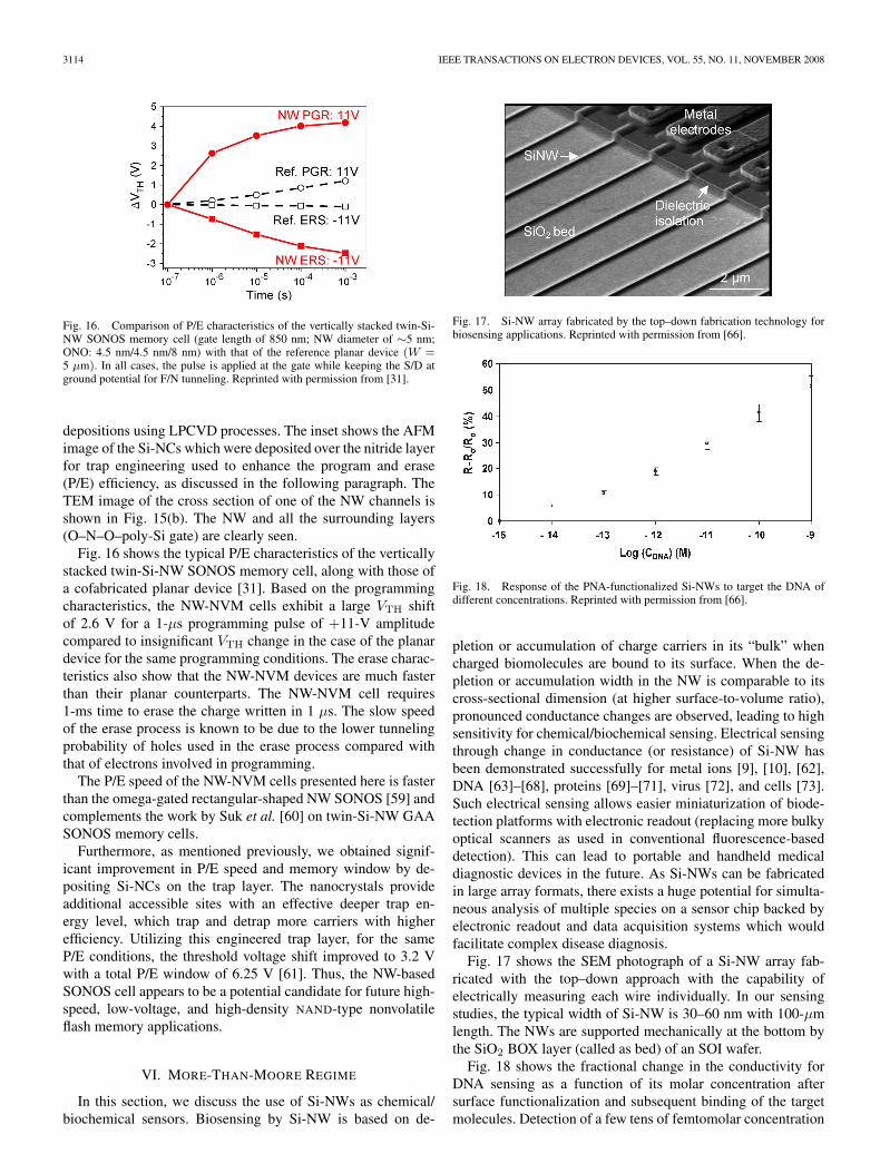
Fig. 16. Comparison of P/E characteristics of the vertically stacked twin-Si-NW SONOS memory cell (gate length of 850 nm; NW diameter of ∼5 nm;ONO: 4.5 nm/4.5 nm/8 nm) with that of the reference planar device (W =5 μm). In all cases, the pulse is applied at the gate while keeping the S/D atground potential for F/N tunneling. Reprinted with permission from [31].
depositions using LPCVD processes. The inset shows the AFMimage of the Si-NCs which were deposited over the nitride layerfor trap engineering used to enhance the program and erase(P/E) efficiency, as discussed in the following paragraph. TheTEM image of the cross section of one of the NW channels isshown in Fig. 15(b). The NW and all the surrounding layers(O–N–O–poly-Si gate) are clearly seen.
Fig. 16 shows the typical P/E characteristics of the verticallystacked twin-Si-NW SONOS memory cell, along with those ofa cofabricated planar device [31]. Based on the programmingcharacteristics, the NW-NVM cells exhibit a large VTH shiftof 2.6 V for a 1-μs programming pulse of +11-V amplitudecompared to insignificant VTH change in the case of the planardevice for the same programming conditions. The erase charac-teristics also show that the NW-NVM devices are much fasterthan their planar counterparts. The NW-NVM cell requires1-ms time to erase the charge written in 1 μs. The slow speedof the erase process is known to be due to the lower tunnelingprobability of holes used in the erase process compared withthat of electrons involved in programming.
The P/E speed of the NW-NVM cells presented here is fasterthan the omega-gated rectangular-shaped NW SONOS [59] andcomplements the work by Suk et al. [60] on twin-Si-NW GAASONOS memory cells.
Furthermore, as mentioned previously, we obtained signif-icant improvement in P/E speed and memory window by de-positing Si-NCs on the trap layer. The nanocrystals provideadditional accessible sites with an effective deeper trap en-ergy level, which trap and detrap more carriers with higherefficiency. Utilizing this engineered trap layer, for the sameP/E conditions, the threshold voltage shift improved to 3.2 Vwith a total P/E window of 6.25 V [61]. Thus, the NW-basedSONOS cell appears to be a potential candidate for future high-speed, low-voltage, and high-density NAND-type nonvolatileflash memory applications.
VI. MORE-THAN-MOORE REGIME
In this section, we discuss the use of Si-NWs as chemical/biochemical sensors. Biosensing by Si-NW is based on de-
Fig. 17. Si-NW array fabricated by the top–down fabrication technology forbiosensing applications. Reprinted with permission from [66].
Fig. 18. Response of the PNA-functionalized Si-NWs to target the DNA ofdifferent concentrations. Reprinted with permission from [66].
pletion or accumulation of charge carriers in its “bulk” whencharged biomolecules are bound to its surface. When the de-pletion or accumulation width in the NW is comparable to itscross-sectional dimension (at higher surface-to-volume ratio),pronounced conductance changes are observed, leading to highsensitivity for chemical/biochemical sensing. Electrical sensingthrough change in conductance (or resistance) of Si-NW hasbeen demonstrated successfully for metal ions [9], [10], [62],DNA [63]–[68], proteins [69]–[71], virus [72], and cells [73].Such electrical sensing allows easier miniaturization of biode-tection platforms with electronic readout (replacing more bulkyoptical scanners as used in conventional fluorescence-baseddetection). This can lead to portable and handheld medicaldiagnostic devices in the future. As Si-NWs can be fabricatedin large array formats, there exists a huge potential for simulta-neous analysis of multiple species on a sensor chip backed byelectronic readout and data acquisition systems which wouldfacilitate complex disease diagnosis.
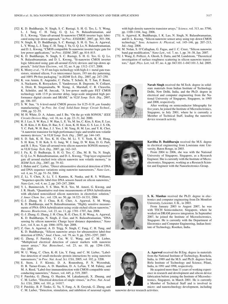
Fig. 17 shows the SEM photograph of a Si-NW array fab-ricated with the top–down approach with the capability ofelectrically measuring each wire individually. In our sensingstudies, the typical width of Si-NW is 30–60 nm with 100-μmlength. The NWs are supported mechanically at the bottom bythe SiO2 BOX layer (called as bed) of an SOI wafer.
Fig. 18 shows the fractional change in the conductivity forDNA sensing as a function of its molar concentration aftersurface functionalization and subsequent binding of the targetmolecules. Detection of a few tens of femtomolar concentration
SINGH et al.: Si, SiGe NANOWIRE DEVICES BY TOP–DOWN TECHNOLOGY AND THEIR APPLICATIONS 3115
Fig. 19. (Left) NMOS VTH box plot and histogram. The VTH for the majorityof devices lies between 0.12 ± 0.05 V. (Right) NMOS ION box plot andhistogram. The ION for the majority of the devices lies between 5.5 ± 0.5 μA.The NW thickness is from 3 to 6 nm. Reprinted with permission from [29].
demonstrates very high sensitivity of these devices [66]. Sen-sitivity can be enhanced further with reduced SiO2 thicknesson top of wires, similar to the case of a classical FET, asthe charges from the attached biomolecules (gate charges) arecloser to the Si-NW surface for better sensing [67].
VII. CHALLENGES AND OPPORTUNITIES
There has been significant progress in fabrication technology,and in understanding of the electrostatics and transport in theGAA NW devices, huge challenges remain to be met beforethis new device architecture reaches the level of manufacturing.The first challenge is large device parameter variability in thethreshold voltage and ION, as shown in Fig. 19. This variabilityis mainly attributed to possible variation of NW shape andsize/diameter and variation in interface quality. Tight controlof the starting fin dimensions with advanced lithography andshape control using H2 annealing may help in reducing thisvariation. The high sensitivity of device parameters, particularlythe VTH to NW size, could possibly be attributed to the vari-ation in silicon-channel-to-oxide-interface quality and changein bandgap as a result of quantum confinement effects [74].Variation in surface roughness could be the possible reason forVTH fluctuations, as an increase in VTH with surface roughnessis speculated [75]. Probabilistic circuit design techniques couldform part of the solution for the successful implementation ofGAA NW devices into manufacturable circuits.
The second challenge pertains to the tuning of the thresholdvoltage. Due to the very limited volume of channel body, thedoping of the channel for VTH adjustment is not feasible. Due tothe cylindrical architecture, the impact of gate oxide thicknesson VTH is also expected to be significantly diminished. Thefeasible solutions lie with the tuning of the gate electrode workfunction and the wire diameters.
The third challenge is in terms of integration density whichis limited by lithographic resolution in the case of top–downCMOS-compatible NWs. However, we believe that with ad-vances in lithography, the integration density of top–down NWswill keep on increasing and may match the extremely highdensity projections using the bottom–up approach. For highdrive currents, as needed, for example, in pad drivers, verticalstacking of NWs could be a solution as that would reducedemand on silicon estate. Another possible option could be
the use of grown NWs for increasing the drive current/devicedensity once the daunting challenges of their manufacturableassembly in circuit functionality are met successfully.
VIII. CONCLUSION
The status of GAA NW CMOS technology using thetop–down approach has been reviewed. The top–down ap-proach is highly integrable in circuit functionality and iscompatible with the existing CMOS technology. NWs andnanostructures seem to have possible novel solutions in the“more-than-Moore” regime of applications such as in the areaof fabrication of chemical/biochemical sensors. The presentedtop–down techniques can potentially address the needs of the“end-of-the-technology roadmap” and beyond CMOS era, pos-sibly with the help of a hybrid approach. Thus, the NW tech-nology indicates feasibility of opening up newer applicationopportunities for Si technology.
ACKNOWLEDGMENT
The authors would like to thank their students at the Instituteof Microelectronics, particularly J. Fu, Y. Jiang, H. Zhou,B. Yang, and G.-J. Zhang, for their contributions to the workpresented in this paper, and their colleagues S. Balakumar,V. Bliznetsov, B. R. Murthy, and S. H. G. Teo for developingvarious process modules for the authors’ NW technology. Theauthors would also like to thank the supporting staff of theirSemiconductor Process Technologies Laboratory for helping inprocessing the wafers.
REFERENCES
[1] G. E. Moore, “Cramming more components onto integrated circuits,”Electron. Mag., vol. 38, no. 8, p. 114, Apr. 19, 1965.
[2] H.-S. P. Wong, “Beyond conventional transistor,” IBM J. Res. Develop.,vol. 46, no. 2/3, pp. 133–168, 2002.
[3] K.-W. Ang, J. Lin, C.-H. Tung, N. Balasubramanian, G. S. Samudra, andY.-C. Yeo, “Strained n-MOSFET with embedded source/drain stressorsand strain-transfer structure (STS) for enhanced transistor performance,”IEEE Trans. Electron Devices, vol. 55, no. 3, pp. 850–857, Mar. 2008.
[4] D. J. Frank, R. H. Dennard, E. Novak, P. M. Solomon, Y. Taur, andH.-S. P. Wong, “Device scaling limits of Si MOSFETs and their applica-tion dependencies,” Proc. IEEE, vol. 89, no. 3, pp. 259–288, Mar. 2001.
[5] M. T. Bohr, R. S. Chau, T. Ghani, and K. Mistry, “The high-k solution,”IEEE Spectr., vol. 44, no. 10, pp. 29–35, Oct. 2007.
[7] L. Chang, Y.-K. Choi, D. Ha, P. Ranade, S. Xiong, J. Bokor, C. Hu, andT.-J. King, “Extremely scaled silicon nano-CMOS devices,” Proc. IEEE,vol. 91, no. 11, pp. 1860–1873, Nov. 2003.
[8] E. Gnani, S. Reggiani, M. Rudan, and G. Baccarani, “Designconsiderations and comparative investigation of ultra-thin SOI, double-gate and cylindrical nanowire FETs,” in Proc. IEEE ESSDERC, 2006,pp. 371–374.
[9] Y. Cui, Q. Wei, H. Park, and C. M. Lieber, “Nanowire nanosensorsfor highly sensitive and selective detection of biological and chemicalspecies,” Science, vol. 293, no. 5533, pp. 1289–1293, Aug. 17, 2001.
[10] G.-J. Zhang, A. Agarwal, D. Buddharaju, N. Singh, and Z. Gao,“Highly sensitive sensors for alkali metal ions based on complementary-metal–oxide–semiconductor-compatible silicon nanowires,” Appl. Phys.Lett., vol. 90, no. 23, pp. 233 903-1–233 903-3, Jun. 2007.
[11] Y. Xia, P. Yang, Y. Sun, Y. Wu, B. Mayers, B. Gates, Y. Yin, F. Kim, andH. Yan, “One-dimensional nanostructures: Synthesis, characterization,and applications,” Adv. Mater., vol. 15, no. 5, pp. 353–389, Mar. 2003.
3116 IEEE TRANSACTIONS ON ELECTRON DEVICES, VOL. 55, NO. 11, NOVEMBER 2008
[12] G. Li, N. Xi, H. Chen, A. Saeed, and M. Yu, “Assembly of nanostructureusing AFM based nanomanipulation system,” in Proc. IEEE Int. Conf.Robot. Autom., 2004, vol. 1, pp. 428–433.
[13] Y. Huang and C. M. Lieber, “Integrated nanoscale electronics and opto-electronics: Exploring nanoscale science and technology through semi-conductor nanowires,” Pure Appl. Chem., vol. 76, no. 12, pp. 2051–2068,2004.
[14] H. Ye, Z. Gu, and D. H. Gracias, “Integrating nanowires with substratesusing directed assembly and nanoscale soldering,” IEEE Trans. Nanotech-nol., vol. 5, no. 1, pp. 62–66, Jan. 2006.
[15] R. He, D. Gao, R. Fan, R. Hochbaum, C. Carraro, R. Maboudian, andP. Yang, “Si nanowire bridges in microtrenches: Integration of growthinto device fabrication,” Adv. Mater., vol. 17, no. 17, pp. 2098–2102,Apr. 2005.
[16] N. A. Melosh, A. Boukai, F. Diana, B. Gerardot, A. Badalato,P. M. Petroff, and J. R. Heath, “Ultrahigh-density nanowire lattices andcircuits,” Science, vol. 300, no. 5616, pp. 112–115, Apr. 2003.
[17] D. W. Wang, B. A. Sheriff, and J. R. Heath, “Complimentary symmetrysilicon nanowire logic: Power-efficient inverters with gain,” Small, vol. 2,no. 10, pp. 1153–1158, 2006.
[18] R. Adelung, O. Cenk Aktas, J. Franc, A. Biswas, R. Kunz, M. Elbahri,J. Kanzow, U. Schürmann, and F. Faupel, “Strain-controlled growth ofnanowires within thin-film cracks,” Nat. Mater., vol. 3, no. 6, pp. 375–379, Jun. 2004.
[19] M. Law, J. Goldberger, and P. Yang, “Semiconductor nanowires andnanotubes,” Annu. Rev. Mater. Res., vol. 34, pp. 83–122, Aug. 2004.
[20] W. Lu and C. M. Lieber, “Semiconductor nanowires,” J. Phys. D, Appl.Phys., vol. 39, no. 21, pp. R387–R406, Oct. 2006.
[21] S. D. Suk, S.-Y. Lee, S.-M. Kim, E.-J. Yoon, M.-S. Kim, M. Li,C. W. Oh, K. H. Yeo, S. H. Kim, D.-S. Shin, K.-H. Lee, H. S. Park, J. Nam,H. C. J. Park, J.-B. Park, D.-W. Kim, D. Park, and B.-I. Ryu, “Highperformance 5 nm radius Twin Silicon Nanowire MOSFET (TSNWFET):Fabrication on bulk Si wafer, characteristics, and reliability,” in IEDMTech. Dig., 2005, pp. 552–555.
[22] T. Tezuka, E. Toyoda, S. Nakaharai, T. Irisawa, N. Hirashita,Y. Moriyama, N. Sugiyama, N. Taoka, Y. Yamashita, O. Kiso, M. Harada,T. Yamamoto, and S. Takagi, “Observation of mobility enhancementin strained Si and SiGe tri-gate MOSFETs with multi-nanowire chan-nels trimmed by hydrogen thermal etching,” in IEDM Tech. Dig., 2007,pp. 887–890.
[23] H. I. Liu, D. K. Biegelsen, N. M. Johnson, F. A. Ponce, andR. F. W. Pease, “Self-limiting oxidation of Si nanowires,” J. Vac. Sci.Technol. B, Microelectron. Process. Phenom., vol. 11, no. 6, pp. 2532–2537, Nov./Dec. 1993.
[24] J. Kedzierski, J. Bokor, and E. Anderson, “Novel method for silicon quan-tum wire transistor fabrication,” J. Vac. Sci. Technol. B, Microelectron.Process. Phenom., vol. 17, no. 6, pp. 3244–3247, Nov./Dec. 1999.
[25] F.-L. Yang et al., “5 nm-gate nanowire FinFET,” in VLSI Symp. Tech. Dig.,2004, pp. 196–197.
[26] T. Ernest et al., “3D stacked nanowires CMOS integration with a dama-scene FinFET process,” in Proc. SSDM, 2007, pp. 200–201.
[27] K. H. Yeo, S. D. Suk, M. Li, Y. Y. Teoh, K. H. Cho, K. H. Hong,S. K. Yun, M. S. Lee, N. M. Cho, K. H. Lee, D. Y. Hwang, B. K. Park,D. W. Kim, D. G. Park, and B. I. Ryu, “Gate-all-around (GAA)twin silicon nanowire MOSFET (TSNWFET) with 15 nm length gate and4 nm radius nanowires,” in IEDM Tech. Dig., 2006, pp. 539–542.
[28] N. Singh, A. Agarwal, L. K. Bera, T. Y. Liow, R. Yang, S. C. Rustagi,C. H. Tung, R. Kumar, G. Q. Lo, N. Balasubramanian, and D.-L. Kwong,“High-performance fully depleted silicon nanowire (diameter ≤ 5 nm)gate-all-around CMOS devices,” IEEE Electron Device Lett., vol. 27,no. 5, pp. 383–386, May 2006.
[29] N. Singh, F. Y. Lim, W. W. Fang, S. C. Rustagi, L. K. Bera, A. Agarwal,C. H. Tung, K. M. Hoe, S. R. Omampuliyur, D. Tripathi, A. O. Adeyeye,G. Q. Lo, N. Balasubramanian, and D. L. Kwong, “Ultra-narrow siliconnanowire gate-all-around CMOS devices: Impact of diameter, channel-orientation and low temperature on device performance,” in IEDM Tech.Dig., 2006, pp. 548–551.
[30] E. J. Tan, K. L. Pey, N. Singh, G. Q. Lo, D. Z. Chi, K. M. Hoe, P. S. Lee,and G. D. Cui, “Silicon nanowire Schottky barrier NMOS transistors,” inProc. SSDM, Tsukuba, Japan, Sep. 18–21, 2007, pp. 816–817.
[31] J. Fu, N. Singh, K. D. Buddharaju, S. H. G. Teo, C. Shen, Y. Jiang,C. X. Zhu, M. B. Yu, G. Q. Lo, N. Balasubramanian, D. L. Kwong,E. Gnani, and G. Baccarani, “Si-nanowire based gate-all-around non-volatile SONOS memory cell,” IEEE Electron Device Lett., vol. 29, no. 5,pp. 518–521, May 2008.
[32] Y. Jiang, N. Singh, T. Y. Liow, W. Y. Loh, S. Balakumar, K. M. Hoe,C. H. Tung, V. Bliznetsov, S. C. Rustagi, G. Q. Lo, D. S. H. Chan, and
D. L. Kwong, “Ge-rich (70%) SiGe nanowire MOSFET fabricated usingpattern-dependent Ge-condensation technique,” IEEE Electron DeviceLett., vol. 29, no. 6, pp. 595–598, Jun. 2008.
[33] L. K. Bera, H. S. Nguyen, N. Singh, T. Y. Liow, D. X. Huang,K. M. Hoe, C. H. Tung, W. W. Fang, S. C. Rustagi, Y. Jiang, G. Q. Lo,N. Balasubramanian, and D. L. Kwong, “Three dimensionally stackedSiGe nanowire array and gate-all-around p-MOSFETs,” in IEDM Tech.Dig., 2006, pp. 1–4.
[34] W. W. Fang, N. Singh, L. K. Bera, H. S. Nguyen, S. C. Rustagi,G. Q. Lo, N. Balasubramanian, and D.-L. Kwong, “Vertically stackedSiGe nanowire array channel CMOS transistors,” IEEE Electron DeviceLett., vol. 28, no. 3, pp. 211–213, Mar. 2007.
[35] N. Singh, W. W. Fang, S. C. Rustagi, K. D. Budharaju, S. H. G. Teo,S. Mohanraj, G. Q. Lo, N. Balasubramanian, and D.-L. Kwong, “Obser-vation of metal-layer stress on Si nanowires in gate-all-around high-κ/metal-gate device structures,” IEEE Electron Device Lett., vol. 28, no. 7,pp. 558–561, Jul. 2007.
[36] Y. Jiang et al., “Low resistivity metallic nanowire contact engineeringfor gate-all-around nanowire transistors with 8 nm gate lengths,” in VLSISymp. Tech. Dig., 2008, pp. 34–35.
[37] G. Zheng, W. Ly, S. Jin, and C. M. Lieber, “Synthesis and fabricationof high-performance n-type silicon nanowire transistors,” Adv. Mater.,vol. 16, no. 21, pp. 1890–1893, Nov. 2004.
[38] Y. Hu, J. Xiang, G. Liang, H. Yan, and C. M. Lieber, “Sub-100 nanome-ter channel length Ge/Si nanowire transistors with potential for 2 THzswitching speed,” Nano Lett., vol. 8, no. 3, pp. 925–930, Mar. 2008.
[39] J. Kavalieros, B. Doyle, S. Datta, G. Dewey, M. Doczy, B. Jin,D. Lionberger, M. Metz, W. Rachmady, M. Radosavljevic, U. Shah,N. Zelick, and R. Chau, “Tri-gate transistor architecture with high-k gatedielectrics, metal gates and strain engineering,” in VLSI Symp. Tech. Dig.,2006, pp. 61–62.
[40] J. Wang, P. Solomon, and M. Lundstrom, “A general approach for the per-formance assessment of nanoscale silicon field effect transistors,” IEEETrans. Electron Device, vol. 51, no. 9, p. 1366, Sep. 2004.
[41] Y. Cui, Z. Zhong, D. Wang, W. U. Wang, and C. M. Lieber, “Highperformance silicon nanowire field effect transistors,” Nano Lett., vol. 3,no. 2, pp. 149–152, Jan. 2003.
[42] R. Tu, L. Zhang, Y. Nishi, and H. Dai, “Measuring the capacitance of in-dividual semiconductor nanowires for carrier mobility assessment,” NanoLett., vol. 7, no. 6, pp. 1561–1565, Jun. 2007.
[43] S. D. Suk, M. Li, Y. Y. Yeoh, K. H. Yeo, K. H. Cho, I. K. Ku, H. Cho,W. J. Jang, D.-W. Kim, and W.-S. Lee, “Investigation of nanowire sizedependency on TSNWFET,” in IEDM Tech. Dig., 2007, pp. 552–555.
[44] H. Ohta, Y. Kim, Y. Shimamune, T. Sakuma, A. Hatada, A. Katakami,T. Soeda, K. Kawamura, H. Kokura, H. Morioka, T. Watanabe, J. Oh,Y. Hayami, J. Ogura, M. Tajima, T. Mori, N. Tamura, M. Kojima, andK. Hashimoto, “High performance 30 nm gate bulk CMOS for 45 nmnode with Σ-shaped SiGe-SD,” in IEDM Tech. Dig., 2005, pp. 247–250.
[45] J.-P. Colinge, L. Floyd, A. J. Quinn, G. Redmond, J. C. Alderman,W. Xiong, C. R. Cleavelin, T. Schulz, K. Schruefer, G. Knoblinger, andP. Patruno, “Temperature effects on trigate SOI MOSFETs,” IEEE Elec-tron Device Lett., vol. 27, no. 3, pp. 172–174, Mar. 2006.
[46] J.-P. Colinge, A. J. Quinn, L. Floyd, G. Redmond, J. C. Alderman,W. Xiong, C. R. Cleavelin, T. Schulz, K. Schruefer, G. Knoblinger, andP. Patruno, “Low-temperature electron mobility in trigate SOIMOSFETs,” IEEE Electron Device Lett., vol. 27, no. 2, pp. 120–122,Feb. 2006.
[47] J.-P. Colinge, J. C. Alderman, W. Xiong, and C. R. Cleavelin, “Quantum-mechanical effects in trigate SOI MOSFETs,” IEEE Trans. Electron De-vices, vol. 53, no. 5, pp. 1131–1136, May 2006.
[48] S. C. Rustagi, N. Singh, Y. F. Lim, G. Zhang, S. Wang, G. Q. Lo,N. Balasubramanian, and D. L. Kwong, “Low-temperature trans-port characteristics and quantum-confinement effects in gate-all-aroundSi-nanowire N-MOSFET,” IEEE Electron Device Lett., vol. 28, no. 10,pp. 909–912, Oct. 2007.
[49] Z. Chen, J. Appenzeller, P. M. Solomon, Y.-M. Lin, and P. Avouris, “Gatework function engineering for nanotube-based circuits,” in Proc. ISSCC,2007, pp. 68–69.
[50] R. S. Friedman, M. C. McAlpine, D. S. Ricketts, D. Ham, andC. M. Lieber, “High-speed integrated nanowire circuits,” Nature, vol. 434,p. 1085, 2005.
[51] S. C. Rustagi, N. Singh, W. W. Fang, K. D. Buddharaju,S. R. Omampuliyur, S. H. G. Teo, C. H. Tung, G. Q. Lo,N. Balasubramanian, and D. L. Kwong, “CMOS inverter based ongate-all-around silicon-nanowire MOSFETs fabricated using top–downapproach,” IEEE Electron Device Lett., vol. 28, no. 11, pp. 1021–1024,Nov. 2007.
SINGH et al.: Si, SiGe NANOWIRE DEVICES BY TOP–DOWN TECHNOLOGY AND THEIR APPLICATIONS 3117
[52] K. D. Buddharaju, N. Singh, S. C. Rustagi, S. H. G. Teo, L. Y. Wong,L. J. Tang, C. H. Tung, G. Q. Lo, N. Balasubramanian, andD. L. Kwong, “Gate-all-around Si-nanowire CMOS inverter logic fabri-cated using top–down approach,” in Proc. ESSDERC, 2007, pp. 303–306.
[53] N. Singh, K. D. Buddharaju, S. C. Rustagi, S. H. G. Teo, A. Agarwal,L. Y. Wong, L. J. Tang, C. H. Tung, J. Yu, G. Q. Lo, N. Balasubramanian,and D. L. Kwong, “CMOS compatible Si-nanowire inverter logic gate forlow power applications,” in Proc. SSDM, 2007, pp. 814–815.
[54] K. D. Buddharaju, N. Singh, S. C. Rustagi, S. H. G. Teo, G. Q. Lo,N. Balasubramanian, and D. L. Kwong, “Si-nanowire CMOS inverterlogic fabricated using gate-all-around (GAA) devices and top–down ap-proach,” Solid State Electron., vol. 52, no. 9, pp. 1312–1317, 2008.
[55] K. Mistry et al., “A 45 nm logic technology with high-k+ metal gate tran-sistors, strained silicon, 9 cu interconnect layers, 193 nm dry patterning,and 100% Pb-free packaging,” in IEDM Tech. Dig., 2007, pp. 247–250.
[56] K. von Arnim, E. Augendre, C. Pacha, T. Schulz, K. T. San, F. Bauer,A. Nackaerts, R. Rooyackers, T. Vandeweyer, B. Degroote, N. Collaert,A. Dixit, R. Singanamalla, W. Xiong, A. Marshall, C. R. Cleavelin,K. Schrüfer, and M. Jurczak, “A low-power multi-gate FET CMOStechnology with 13.9 ps inverter delay, large-scale integrated high per-formance digital circuits and SRAM,” in VLSI Symp. Tech. Dig., 2007,pp. 106–107.
[57] S. W. Sun, “A 6-level-metal CMOS process for 0.25–0.18 μm foundrymanufacturing,” in Proc. Int. Conf. Solid-State Integr. Circuit Technol.,1998, pp. 52–55.
[58] M. H. White, D. A. Adams, and J. Bu, “On the go with SONOS,” IEEECircuits Devices Mag., vol. 16, no. 4, pp. 22–31, Jul. 2000.
[59] H. J. Lee, S. W. Ryu, J. W. Han, L. E. Yu, M. Im, C. Kim, S. Kim, E. Lee,K. H. Kim, J. H. Kim, D. Bae, S. C. Jeon, K. H. Kim, G. S. Lee, J. S. Oh,Y. C. Park, W. H. Bae, J. J. Yoo, J. M. Yang, H. M. Lee, and Y. K. Choi,“A nanowire transistor for high performance logic and terabit non-volatilememory devices,” in VLSI Symp. Tech. Dig. , 2007, pp. 144–145.
[60] S. D. Suk, K. H. Yeo, K. H. Cho, M. Li, Y. Y. Yeoh, K. H. Hong,S. H. Kim, Y. H. Koh, S. G. Jung, W. J. Jang, D. W. Kim, D. G. Park,and B. I. Ryu, “Gate-all-around twin silicon nanowire SONOS memory,”in VLSI Symp. Tech. Dig., 2007, pp. 142–143.
[61] J. Fu, K. D. Budharaju, S. H. G. Teo, C. Zhu, M. B. Yu, N. Singh,G. Q. Lo, N. Balasubramanian, and D.-L. Kwong, “Trap layer engineeredgate all around stacked twin silicon nanowire non volatile memory,” inIEDM Tech. Dig., 2007, pp. 79–82.
[62] J. Hahm and C. Lieber, “Direct ultrasensitive electrical detection of DNAand DNA sequence variations using nanowire nanosensors,” Nano Lett.,vol. 4, no. 51, pp. 51–54, 2004.
[63] Z. Li, Y. Chen, X. Li, T. I. Kamins, K. Nauka, and R. S. Williams,“Sequence-specific label-free DNA sensors based on silicon nanowires,”Nano Lett., vol. 4, no. 2, pp. 245–247, 2004.
[64] Y. L. Bunimovich, Y. S. Shin, W.-S. Yeo, M. Amori, G. Kwong, andJ. R. Heath, “Quantitative real-time measurements of DNA hybridizationwith alkylated nonoxidized silicon nanowires in electrolyte solution,”J. Amer. Chem. Soc., vol. 128, no. 50, pp. 16 323–16 331, 2006.
[65] G.-J. Zhang, H. J. Chua, R.-E. Chee, A. Agarwal, S. M. Wong,K. D. Buddharaju, and N. Balasubramanian, “Highly sensitive measure-ments of PNA–DNA hybridization using oxide-etched silicon nanowire,”Biosens. Bioelectron., vol. 23, no. 11, pp. 1701–1707, Jun. 2008.
[66] G.-J. Zhang, G. Zhang, J. H. Chua, R.-E. Chee, E. H. Wong, A. Agarwal,K. D. Buddharaju, N. Singh, Z. Gao, and N. Balasubramanian, “DNAsensing by silicon nanowire: Charge layer distance dependence,” NanoLett., vol. 8, no. 4, pp. 1066–1070, Apr. 2008.
[67] Z. Gao, A. Agarwal, A. D. Trigg, N. Singh, C. Fang, C. H. Tung, andK. D. Buddharaju, “Silicon nanowire arrays for ultrasensitive label-freedetection of DNA,” Anal. Chem., vol. 79, no. 9, pp. 3291–3297, 2007.
[68] G. Zheng, F. Patolsky, Y. Cui, W. U. Wang, and C. M. Lieber,“Multiplexed electrical detection of cancer markers with nanowiresensor arrays,” Nat. Biotechnol., vol. 23, no. 10, pp. 1294–1301,Oct. 2005.
[69] W. U. Wang, C. Chen, K.-H. Lin, Y. Fang, and C. M. Lieber, “Label-free detection of small-molecule–protein interactions by using nanowirenanosensors,” in Proc. Nat. Acad. Sci. USA, 2005, vol. 102, p. 3208.
[70] E. Stern, J. F. Klemic, D. A. Routenberg, P. N. Wyrembak,D. B. Turner-Evans, A. D. Hamilton, D. A. LaVan, T. M. Fahmy, andM. A. Reed, “Label-free immunodetection with CMOS-compatible semi-conducting nanowires,” Nature, vol. 445, p. 519, 2007.
[71] F. Patolsky, G. Zheng, O. Hayden, M. Lakadamyali, X. Zhuang, andC. M. Lieber, “Electrical detection of single viruses,” in Proc. Nat. Acad.Sci. USA, 2004, vol. 101, p. 14 017.
[72] F. Patolsky, B. P. Timko, G. Yu, Y. Fang, A. B. Greytak, G. Zheng, andC. M. Lieber, “Detection, stimulation, and inhibition of neuronal signals
with high-density nanowire transistor arrays,” Science, vol. 313, no. 5790,pp. 1100–1104, Aug. 2006.
[73] A. Agarwal, K. Buddharaju, I. K. Lao, N. Singh, N. Balasubramanian,and D. L. Kwong, “Silicon nanowire sensor array using top–down CMOStechnology,” Sens. Actuators A: Physical, vol. 145–146, pp. 207–213,Jul.–Aug. 2008.
[74] M. Nolan, S. O’Callaghan, G. Fagas, and J. C. Creer, “Silicon nanowireband gap modification,” Nano Lett., vol. 7, no. 1, pp. 34–38, Jan. 2007.
[75] J. Wang, E. Pollizzi, A. Ghosh, S. Datta, and M. Lundstrom, “Theoreticalinvestigation of surface roughness scattering in silicon nanowire transis-tors,” Appl. Phys. Lett, vol. 87, no. 4, pp. 043 101-1–043 101-3, Jul. 2005.
Navab Singh received the M.Tech. degree in solid-state materials from Indian Institute of TechnologyDelhi, New Delhi, India, and the Ph.D. degree inelectrical and computer engineering from the Na-tional University of Singapore, Singapore, in 1995and 2008, respectively.
After working on semiconductor lithography forfive years, he joined the Institute of Microelectronics,Singapore, in July 2001, where he is currently aMember of Technical Staff, leading the nanowiredevice research activity.
Kavitha D. Buddharaju received the M.S. degreein electrical engineering from Louisiana state Uni-versity, Baton Rouge, in 2003.
From 2004 to 2006, she was with the NationalUniversity of Singapore, Singapore, as a ResearchEngineer. She is currently with the Institute of Micro-electronics, Singapore, working as a Research Scien-tist and Engineer with the Nanoelectronics Group.
S. K. Manhas received the Ph.D. degree in elec-tronics and computer engineering from De MontfortUniversity, Leicester, U.K., in 2003.
From January 2003 to August 2007, he waswith TECH Semiconductor, Singapore, where heworked on DRAM process integration. In September2007, he joined the Institute of Microelectronics,Singapore. He is currently with the Department ofElectronics and Computer Engineering, Indian Insti-tute of Technology, Roorkee, India.
A. Agarwal received the B.Eng. degree in materialsfrom the National Institute of Technology, Rourkela,India, in 1989 and the M.S. and Ph.D. degrees fromBirla Institute of Technology and Science, Pilani,India, in 1991 and 1998, respectively.
He acquired more than 11 years of working experi-ence in research and development and silicon devicefabrication before joining the Institute of Microelec-tronics, Singapore, in March 2001. He is currentlya Member of Technical Staff and is involved inmicro- and nanotechnology development, including
nanowire device research activities.
3118 IEEE TRANSACTIONS ON ELECTRON DEVICES, VOL. 55, NO. 11, NOVEMBER 2008
Subhash C. Rustagi received the Ph.D. degree inphysics from Kurukshetra University, Kurukshetra,India, in 1980.
In 1982, he joined CARE, Indian Institute ofTechonology, Delhi, India. Since 1999, he has beenwith the Institute of Microelectronics, Singapore,where he is currently a Member of Technical Staff,working on modeling and transport in nanowireCMOS devices.
G. Q. Lo received the Ph.D. degree in electrical andcomputer engineering from the University of Texas,Austin, in 1992.
After being with Integrated Device Technology,Inc., for 12 years, he joined the Institute of Mi-croelectronics, Singapore, where he is currently theDirector for Nanoelectronics and Photonics Programand Semiconductor Process Technology Laboratory.
N. Balasubramanian received the Ph.D. degree inphysics from Indian Institute of Technology, Madras,India, in 1990.
He was an Engineering Section Manager forCMOS front-end technologies with CharteredSemiconductor Manufacturing Ltd., Singapore.In 1998, he joined the Institute of Microelectronics,Singapore, where he held various positions,including Director for Semiconductor ProcessTechnology and Director for Bioelectronics andBioMEMS Program. Since April 2008, he has been
with Silterra, Kulim, Malaysia.
Dim-Lee Kwong received the Ph.D. degree fromRice University, Houston, TX.
Since 2005, he has been with the Institute ofMicroelectronics, Singapore, as the Executive Direc-tor. Prior to that, he was a Professor of electricaland computer engineering and held an Earl N. andMargaret Brasfield Endowed Professorship with theUniversity of Texas, Austin, and a Temasek Pro-fessor with the National University of Singapore,Singapore. He has supervised more than 54 Ph.D.students.