Duljit S. Malhi, Member, IEEE, Lawrence E. Larson, Fellow, IEEE, Dawn Wang, Cuneyt Demirdag, andVictoria Pereira
Abstract—This paper presents the design considerations andexperimental results of a transmitter integrated circuit (IC) forwide-band code division multiple access (W-CDMA) mobileterminal application based on a superheterodyne architecture.Implemented by utilizing IBM’s 0.5- m SiGe BiCMOS tech-nology, the transmitter IC consumes approximately 270 mWwith a 3.0-V power supply. The radio-frequency IC features athird-order output intercept point (OIP3) of +25.0 dBm, a 95-dBdynamic range, and 6.3% error vector magnitude.
Index Terms—Automatic gain control, baluns, error vector mag-nitude, wideband code division multiple access (W-CDMA).
I. INTRODUCTION
W IRELESS communication is evolving rapidly fromlow-bit-rate voice services to high-bit-rate multimedia
applications. Internet access and video and picture transferservices are key drivers. These applications require a few tensof kilobits per second to approximately 2 Mb/s data rate. Thus,the capability targets for the third-generation (3G) cellularsystem have been defined as 144 kb/s for high-speed vehiculartraffic, 384 kb/s for pedestrian or low-speed vehicular traffic,and 2 Mb/s for indoor offices and/or local wireless loops. Thestandardization of the 3G cellular systems [1] is quite matureand systems are in deployment state. The systems are knownas UMTS or IMT-2000. In Europe and Japan, the wide-bandcode-division multiple-access (W-CDMA) scheme has beenadopted as the air interface [2]–[3]. The W-CDMA mobile ter-minals or User Equipment (UE) Power Class 3 are targeted fora maximum transmission power of24 dBm and a minimumof 50 dBm power levels at the antenna, which translatesinto 74 dB of dynamic range. To account for manufacturingprocesses, operating temperature, and power supply variation,extra margin in the dynamic range is essential. At the antenna,the adjacent channel leakage ratio (ACLR), which determineshow much of the mobile terminal’s transmitted power is
Manuscript received November 18, 2002; revised April 10, 2003.D. S. Malhi was with TriQuint Semiconductor, Lowell, MA 01854 USA. He
is now with Synopsys, Mississauga, ON L5B 1M2, Canada (e-mail: [email protected]).
L. E. Larson is with the Center for Wireless Communications, Department ofElectrical and Computer Engineering, University of California at San Diego, LaJolla, CA 92093 USA (e-mail: [email protected]).
D. Wang was with IBM, Lowell, MA 01852 USA. She is now with TriQuintSemiconductor, Lowell, MA 01854 USA.
C. Demirdag was with IBM, Lowell, MA 01852 USA. He is now with Kenet,Inc., Reading, MA 01867 USA.
V. Pereira was with IBM, Lowell, MA 01852 USA. She is now with NorthropGrumman, Palm Harbor, FL 34683 USA.
Digital Object Identifier 10.1109/JSSC.2003.815908
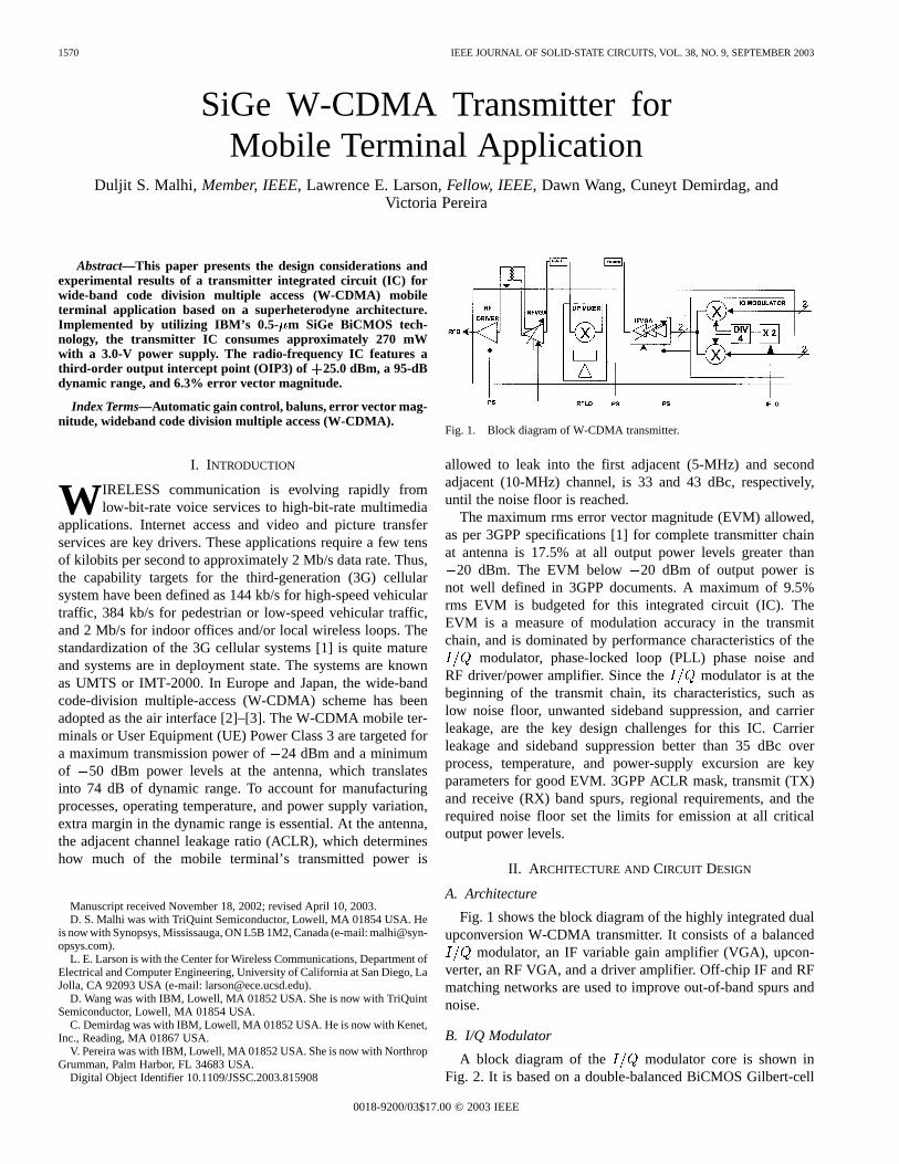
Fig. 1. Block diagram of W-CDMA transmitter.
allowed to leak into the first adjacent (5-MHz) and secondadjacent (10-MHz) channel, is 33 and 43 dBc, respectively,until the noise floor is reached.
The maximum rms error vector magnitude (EVM) allowed,as per 3GPP specifications [1] for complete transmitter chainat antenna is 17.5% at all output power levels greater than
20 dBm. The EVM below 20 dBm of output power isnot well defined in 3GPP documents. A maximum of 9.5%rms EVM is budgeted for this integrated circuit (IC). TheEVM is a measure of modulation accuracy in the transmitchain, and is dominated by performance characteristics of the
modulator, phase-locked loop (PLL) phase noise andRF driver/power amplifier. Since the modulator is at thebeginning of the transmit chain, its characteristics, such aslow noise floor, unwanted sideband suppression, and carrierleakage, are the key design challenges for this IC. Carrierleakage and sideband suppression better than 35 dBc overprocess, temperature, and power-supply excursion are keyparameters for good EVM. 3GPP ACLR mask, transmit (TX)and receive (RX) band spurs, regional requirements, and therequired noise floor set the limits for emission at all criticaloutput power levels.
II. A RCHITECTURE ANDCIRCUIT DESIGN
A. Architecture
Fig. 1 shows the block diagram of the highly integrated dualupconversion W-CDMA transmitter. It consists of a balanced
modulator, an IF variable gain amplifier (VGA), upcon-verter, an RF VGA, and a driver amplifier. Off-chip IF and RFmatching networks are used to improve out-of-band spurs andnoise.
B. I/Q Modulator
A block diagram of the modulator core is shown inFig. 2. It is based on a double-balanced BiCMOS Gilbert-cell
MALHI et al.: SiGe W-CDMA TRANSMITTER FOR MOBILE TERMINAL APPLICATION 1571
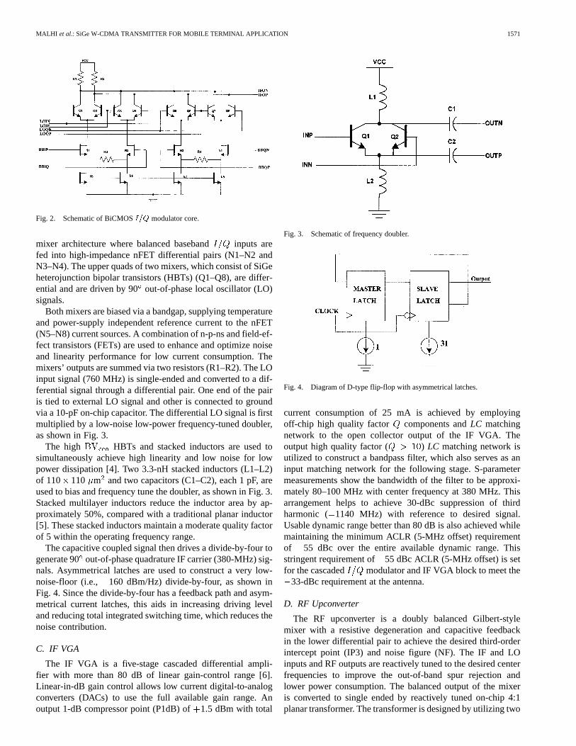
Fig. 2. Schematic of BiCMOSI=Q modulator core.
mixer architecture where balanced baseband inputs arefed into high-impedance nFET differential pairs (N1–N2 andN3–N4). The upper quads of two mixers, which consist of SiGeheterojunction bipolar transistors (HBTs) (Q1–Q8), are differ-ential and are driven by 90out-of-phase local oscillator (LO)signals.
Both mixers are biased via a bandgap, supplying temperatureand power-supply independent reference current to the nFET(N5–N8) current sources. A combination of n-p-ns and field-ef-fect transistors (FETs) are used to enhance and optimize noiseand linearity performance for low current consumption. Themixers’ outputs are summed via two resistors (R1–R2). The LOinput signal (760 MHz) is single-ended and converted to a dif-ferential signal through a differential pair. One end of the pairis tied to external LO signal and other is connected to groundvia a 10-pF on-chip capacitor. The differential LO signal is firstmultiplied by a low-noise low-power frequency-tuned doubler,as shown in Fig. 3.
The high HBTs and stacked inductors are used tosimultaneously achieve high linearity and low noise for lowpower dissipation [4]. Two 3.3-nH stacked inductors (L1–L2)of 110 110 m and two capacitors (C1–C2), each 1 pF, areused to bias and frequency tune the doubler, as shown in Fig. 3.Stacked multilayer inductors reduce the inductor area by ap-proximately 50%, compared with a traditional planar inductor[5]. These stacked inductors maintain a moderate quality factorof 5 within the operating frequency range.
The capacitive coupled signal then drives a divide-by-four togenerate 90out-of-phase quadrature IF carrier (380-MHz) sig-nals. Asymmetrical latches are used to construct a very low-noise-floor (i.e., 160 dBm/Hz) divide-by-four, as shown inFig. 4. Since the divide-by-four has a feedback path and asym-metrical current latches, this aids in increasing driving leveland reducing total integrated switching time, which reduces thenoise contribution.
C. IF VGA
The IF VGA is a five-stage cascaded differential ampli-fier with more than 80 dB of linear gain-control range [6].Linear-in-dB gain control allows low current digital-to-analogconverters (DACs) to use the full available gain range. Anoutput 1-dB compressor point (P1dB) of1.5 dBm with total
Fig. 3. Schematic of frequency doubler.
Fig. 4. Diagram of D-type flip-flop with asymmetrical latches.
current consumption of 25 mA is achieved by employingoff-chip high quality factor components andLC matchingnetwork to the open collector output of the IF VGA. Theoutput high quality factor ( ) LC matching network isutilized to construct a bandpass filter, which also serves as aninput matching network for the following stage. S-parametermeasurements show the bandwidth of the filter to be approxi-mately 80–100 MHz with center frequency at 380 MHz. Thisarrangement helps to achieve 30-dBc suppression of thirdharmonic ( 1140 MHz) with reference to desired signal.Usable dynamic range better than 80 dB is also achieved whilemaintaining the minimum ACLR (5-MHz offset) requirementof 55 dBc over the entire available dynamic range. Thisstringent requirement of 55 dBc ACLR (5-MHz offset) is setfor the cascaded modulator and IF VGA block to meet the
33-dBc requirement at the antenna.
D. RF Upconverter
The RF upconverter is a doubly balanced Gilbert-stylemixer with a resistive degeneration and capacitive feedbackin the lower differential pair to achieve the desired third-orderintercept point (IP3) and noise figure (NF). The IF and LOinputs and RF outputs are reactively tuned to the desired centerfrequencies to improve the out-of-band spur rejection andlower power consumption. The balanced output of the mixeris converted to single ended by reactively tuned on-chip 4:1planar transformer. The transformer is designed by utilizing two
1572 IEEE JOURNAL OF SOLID-STATE CIRCUITS, VOL. 38, NO. 9, SEPTEMBER 2003
Fig. 5. Layout of cross-coupled planer transformer.
Fig. 6. Lumped model of planer 4:1 transformer.
pairs of tightly coupled inductors, one of which is connected inseries and other in parallel to achieve a 4:1 inductance ratio. Itis necessary to use capacitive tuning to minimize the insertionloss of the transformer. The transformer has minimum insertionloss when used for a 4:1 impedance transformation ratio, butcan be used for higher or lower impedance ratios with increasedinsertion loss [5], [7]. Due to the true differential nature ofboth the input and output ports, it allows us to interface differ-entially with an off-chipLC bandpass filter or single-ended,whichever provides optimum performance. The layout of theeach tightly coupled pair of inductors (half transformer) hasa size of 266 266 m . The full transformer is shown inFig. 5. To achieve 3-dB insertion loss, 4-m-thick 10- m-widetop-level metal is used to design the coupled inductors and athin lower metal layer is used for the underpass. The lumpedmodel of the complete transformer is shown in Fig. 6. All fourtightly coupled inductors (L1–L4) and corresponding resistors(R7–R10), which determine the quality factor of individualinductors, carry the same value. C7 and C8 are couplingcapacitors between the tightly coupled inductors. CapacitorsC1–C6 and resistors R1–R6 represent substrate loss.
The coupling coefficients, represented by K1 and K2, are ap-proximately 0.7 for this transformer. The mixer core and LObuffer are precisely biased by an on-chip bandgap circuit andoff-chip precision resistor to tailor the bias current to achieve op-timum overall performance. The measured conversion gain, NF,and output P1dB over process, temperature, and power-supplyvariation are within 5% of nominal values, which are 3, 11, and
0.0 dBm, respectively. The LO-to-RF, IF-to-RF, and LO-to-IFisolations are 34, 32, and 60 dB, respectively.
E. RF VGA
RF amplification and variable gain function at 1.95 GHz isperformed with a class-A VGA. The single-stage VGA is basedon current-steering architecture for gain control. It is temper-ature and process compensated and offers 30-dB gain-controlrange and 18 dB of gain. It consumes only 28 mA while pro-viding 7 dBm output P1dB and 5-dB NF. Open collectors ofthe RF VGA allow greater off-chip and on-chip matching flex-ibility to improve linearity, gain, and single-ended or differen-tial operation. In this particular version of the transmitter, anoff-chip RF transformer is used to convert balanced outputs tounbalanced signal. This off-chip flexibility helps in controllingcascaded performance in optimizing the first iteration of the in-tegrated design.
F. Class-AB Driver
The class-AB driver is a single-ended single-stage common-emitter amplifier with C-B negative feedback for improved sta-bility and linearity. The Class-AB design was chosen to achievehigh linearity and low noise for minimum bias current of 16 mA.High-breakdown ( ) high-linearity SiGe HBTs [8], [9] areused to achieve very high linearity for low quiescent currentconsumption. The driver provides 14-dB gain, 4-dB NF, and
15-dBm output P1dB while consuming only 16 mA of quies-cent current at 7-dBm output power. Again, the open collectordesign allows higher low-loss off-chip matching. It also pro-vides an added flexibility in optimizing power gain and ACLRfor an optimum performance interface with the high-power am-plifier (HPA). This amplifier has a gain variation of less than
2 dB over process and1 dB over temperature and supplyvoltage, permitting manufacturing to take place with no expen-sive tuning or calibration.
III. EXPERIMENTAL RESULTS
A transmitter IC for W-CDMA mobile terminal applicationwas implemented using IBM 0.5-m SiGe BiCMOS produc-tion technology. This technology offers dual breakdown SiGeHBTs and CMOS devices as well as planar inductors. Customstacked inductors and transformers are developed to implementhigh-density integrated RF circuits with optimum performance.A photomicrograph of the chip is shown in Fig. 7. The activearea of the IC is 2.54 mm 2.54 mm and is compatiblefor a 32-pin exposed-paddle BCC32++ or QFN32 package.Measurements of individual building blocks and fully cascadedTX chains were performed. The total power dissipation ofapproximately 270 mW was achieved with a 3.0-V typicalvoltage supply. The IF LO was chosen at a fixed frequency of760 MHz and the RF LO was varied from 1540 to 1600 MHz.Both continuous-wave (CW) and hybrid phase shift keying(HPSK) modulated input signals were used to characterize theTX IC for dynamic range, linearity, noise, spurs, and EVM. Aninput sine-wave signal of 500 kHz frequency with varied inputvoltage swing (i.e., typical 1.0 V differential) was used to
MALHI et al.: SiGe W-CDMA TRANSMITTER FOR MOBILE TERMINAL APPLICATION 1573
Fig. 7. Photomicrograph of chip.
Fig. 8. Measured adjacent and alternate channel characteristics for+7.0-dBmoutput power.
measure the input and output P1dB and dynamic range of theintegrated IC. Cascaded input P1dB of 4.0 Vdifferential andoutput P1dB of 15 dBm was measured.
The typical HPSK modulated input signal of 1.3 V dif-ferential with a peak-to-average ratio of multimode transmissionof approximately 6 dB, as well as a chip rate of 3.84 MHz anda Kaiser window ( ) was used to measure ACLR, ACLRmask, and EVM. The close-in or TX band noise floor is spec-ified in the spectrum emission mask. Fig. 8 shows the detailedACLR measurement as per 3GPP requirements for an output of
7 dBm at 5 MHz and 10-MHz offset. The CW measure-ment also shows that the TX and RX band noise floor is less than
130 dBm/Hz and 150 dBm/Hz, respectively. The TX bandnoise floor improves as the output power levels are reduced. TheRX band noise floor remains constant over the whole dynamicrange.
Fig. 9 shows the modulated output power of TX IC versusACLR at 5-MHz offset for both up and down channels. It canbe seen that the ACLR of 49 dBc for7-dBm modulated powercan be achieved at5-MHz offset. It is well above the minimum
Fig. 9. Modulated output power versus ACLR.
Fig. 10. Measured HPSK constellation for output power of+7 dBm.
requirement of 33 dBc at the antenna for the complete trans-mitter including the HPA stage.
The Advantest R3267/73 test setup was used to analyze con-stellation and EVM characteristics. The measured worst caseEVM is less than 6.3%, which is sufficiently small to satisfy the9.5% budgeted for this IC. The constellation plot of HPSK mod-ulated signal is shown in Fig. 10.
IV. CONCLUSION
A highly integrated and production RF transmitter IC de-signed in IBM’s 0.5- m SiGe BiCMOS process has been pre-sented for W-CDMA applications satisfying or exceeding all3GPP requirements. For a typical output modulated power of
7 dBm, 49-dBc ACLR at 5-MHz offset, TX band noise floorof 141 dBm/Hz at 8.5-MHz offset for low output power levels,RX band noise floor of 144 dBm/Hz for all output signallevels, and rms EVM of 6.3% are achieved. The IC consumes270 mW of total power for 3.0-V typical voltage supply.
ACKNOWLEDGMENT
The authors would like to thank Dr. K. Itoh, H. Joba,Y. Matsunami, S. Shinju, and Dr. N. Suematsu of Mitsubishi
1574 IEEE JOURNAL OF SOLID-STATE CIRCUITS, VOL. 38, NO. 9, SEPTEMBER 2003
Electric Corporation for their contributions and for manyvaluable discussions. They would also like to thank G. Lindsayand S. Simmers for layout, L. Prestia, R. Festa, S. McGoldrick,and M. Deering for measurements, B. Mangla and his team formanufacturing support, and J. Ardizzoni for application notes.
REFERENCES
[1] The 3rd Generation Partnership Project. (1998–2003). [Online]. Avail-able: http://www.3gpp.org
[2] E. Dahlmann, P. Beming, J. Knutsson, F. Ovesgo, M. Persson, and C.Roobol, “W-CDMA—The radio interface for future mobile multimediacommunications,”IEEE Trans. Veh. Technol., vol. 47, pp. 1105–1118,Nov. 1998.
[3] L. B. Milstein, “Wideband code division multiple access,”IEEE J. Se-lect. Areas Commun., vol. 18, pp. 1344–1354, Aug. 2000.
[4] D. Wang, K. Krishnamurthi, S. Gibson, and J. Brunt, “A 2.5-GHz lownoise high linearity LNA/Mixer IC in SiGe BiCMOS technology,” inIEEE Radio Frequency Integrated Circuit Symp. Dig. Papers, May 2001,pp. 249–252.
[5] L. Tao, J. Gillis, D. Wang, and P. Cooper, “Design and modeling of com-pact on-chip transformer/balun using multi-level metal winding for RFintegrated circuits,” inIEEE Radio Frequency Integrated Circuit Symp.Dig. Papers, May 2001, pp. 117–120.
[6] H. Joba, Y. Takahashi, Y. Matsunami, K. Itoh, S. Shinjo, N. Suematsu, D.S. Malhi, D. Wang, K. Schelkle, and P. Bacon, “W-CDMA SiGe TX-ICwith high dynamic range and high power control accuracy,” inIEEERadio Frequency Integrated Circuit Symp. Dig. Papers, June 2002, pp.27–30.
[7] J. Long, “Monolithic transformers for silicon RF IC design,”IEEE J.Solid-State Circuits, vol. 35, pp. 1368–1382, Sept. 2000.
[8] G. Niu, Q. Liang, J. D. Cressler, C. S. Webster, and D. L. Harame,“RF linearity characteristics of SiGe HBT’s,”IEEE Trans. MicrowaveTheory Tech., vol. 49, pp. 1558–1565, Sept. 2001.
[9] S. Shinjo, K. Mori, H. Joba, and N. Suematsu, “Low quiescent currentmirror type self bias control circuit,” inProc. Eur. Microwave Conf., vol.3, 2001, pp. 207–210.
Duljit S. Malhi (M’01) received the B.Sc. and M.Sc.degrees from the University of Delhi, Delhi, India, in1979 and 1981, respectively, the M.Tech. degree fromthe Indian Institute of Technology, Delhi, in 1983,and the M.A.Sc. degree in electrical engineering fromthe University of Toronto, Toronto, ON, Canada, in1991.
From 1990 to 1999, he was with Nortel Networks,Ottawa, ON, as a Senior Member of Scientific Staffworking on the design of various analog and digitalintegrated circuits in various internal and external Si
and SiGe BiCMOS technologies for their application in optical and wirelessnetworks. From 1999 to 2003, he was with IBM and its divestiture TriQuintSemiconductor, where he built various RF and mixed-signal integrated circuitsfor their application in third-generation (3G) wireless handsets. He is currentlywith Synopsys, Mississauga, ON, as a Senior R&D Engineer. He has publishedover 14 research papers in various IEEE journals and conferences and has re-ceived four U.S. patents. His current research interests include building RF andmixed-signal systems-on-chip for wireless and wireline applications.
Lawrence E. Larson(S’82–M’86–SM’90–F’00) re-ceived the B.S. and M. Eng. degrees in electrical engi-neering from Cornell University, Ithaca, NY, in 1979and 1980, respectively, the Ph.D. degree in electricalengineering and MBA degree from the University ofCalifornia at Los Angeles in 1986 and 1996, respec-tively.
From 1980 to 1996, he was with Hughes ResearchLaboratories, Malibu, CA, where he directed thedevelopment of high-frequency microelectronicsin GaAs, InP, Si/SiGe, and MEMS technologies.
He joined the faculty of the University of California at San Diego (UCSD),La Jolla, in 1996, where he is the Inaugural Holder of the CommunicationsIndustry Chair. He is currently Director of the UCSD Center for WirelessCommunications. During the 2000–2001 academic year, he was on leave withIBM Research, San Diego, where he directed the development of RFICs forthird-generation applications. He has published over 150 papers, coauthoredthree books, and holds 25 U.S. patents.
Dr. Larson was the recipient of the 1995 Hughes Electronics Sector PatentAward for his work on RF MEMs, a corecipient of the 1996 Hughes ElectronicsLawrence A. Hyland Patent Award for his work on low-noise millimeter-waveHEMTs, and the 1999 IBM Microelectronics Excellence Award for his work inSi/SiGe HBT technology.
Dawn Wang received the B.S.E.E. and M.S.E.E. de-grees from Tsinghua University, Beijing, China, andthe M.S. degree in solid-state physics from ArizonaState University, Tempe.
She was with Texas Instruments of Tucsonfrom 1995 to 1998, where she was involvedwith device electrical characterization and analogand mixed-signal product engineering. In 1998,she joined the Boston Wireless Design Center,IBM Microelectronics, Lowell, MA, focusing onfront-end highly integrated RF IC designs in SiGe
BiCMOS technology for handset applications. She was also actively engagedwith the IBM technology development team to define high-performancedevices for RF applications. Since June 2002, she has been with TriQuintSemiconductors, Boston, MA, working on SiGe power amplifier circuit designand characterization. She has published more than ten technical papers in RFIC design areas.
Cuneyt Demirdag received the B.S. degree inelectrical engineering from the Middle East Tech-nical University, Ankara, Turkey, in 1995 and theM.S.E.E. degree from The Ohio State University,Columbus, in 1997.
From 1997 to 2000, he was a Design Engineer withFujitsu Microelectronics, Dallas, TX. From 2000 to2002, he was a Design Engineer with the W-CDMAchipset development team at IBM Microelectronics,Lowell, MA. In 2002, he joined Kenet Inc., Reading,MA. His main research interests are in RF and analog
IC designs.
Victoria Pereira received the B.S. degree in elec-trical engineering from the University of SouthernCalifornia, Los Angeles, in 1990.
She was with Hughes Electronics, now Raytheon,from 1990 to 1996 designing mixed-signal analogICs, hybrid and module for radar applications. Shetransferred to Raytheon Advanced Products to workon high-speed converter designs in IC, hybrid andmodule design from 1996 to 1999. She joined theIBM Wireless Design Center in 1999, where shewas involved in developing transceiver ICs for
handset applications using IBM’s SiGe process. She is currently with NorthropGrumman, Palm Harbor, FL, where she is involved in high-end integratedcommunication ICs in 0.35-�m SiGe process.