SANDIA REPORT SAND2009-6759 Unlimited Release Printed October 2009 Simulation of Ion Beam Induced Current in Radiation Detectors and Microelec- tronic Devices Gyorgy Vizkelethy Prepared by Sandia National Laboratories Albuquerque, New Mexico 87185 and Livermore, California 94550 Sandia is a multiprogram laboratory operated by Sandia Corporation, a Lockheed Martin Company, for the United States Department of Energy’s National Nuclear Security Administration under Contract DE-AC04-94AL85000. Approved for public release; further dissemination unlimited.
Transcript
SANDIA REPORT SAND2009-6759 Unlimited Release Printed October 2009
Simulation of Ion Beam Induced Current in Radiation Detectors and Microelec-tronic Devices Gyorgy Vizkelethy Prepared by Sandia National Laboratories Albuquerque, New Mexico 87185 and Livermore, California 94550 Sandia is a multiprogram laboratory operated by Sandia Corporation, a Lockheed Martin Company, for the United States Department of Energy’s National Nuclear Security Administration under Contract DE-AC04-94AL85000. Approved for public release; further dissemination unlimited.
2
Issued by Sandia National Laboratories, operated for the United States Department of Energy by Sandia Corporation. NOTICE: This report was prepared as an account of work sponsored by an agency of the United States Government. Neither the United States Government, nor any agency thereof, nor any of their employees, nor any of their contractors, subcontractors, or their employees, make any warranty, express or implied, or assume any legal liability or responsibility for the accuracy, completeness, or usefulness of any information, apparatus, product, or process dis-closed, or represent that its use would not infringe privately owned rights. Reference herein to any specific commercial product, process, or service by trade name, trademark, manufacturer, or otherwise, does not necessarily constitute or imply its endorsement, recommendation, or fa-voring by the United States Government, any agency thereof, or any of their contractors or subcontractors. The views and opinions expressed herein do not necessarily state or reflect those of the United States Government, any agency thereof, or any of their contractors. Printed in the United States of America. This report has been reproduced directly from the best available copy. Available to DOE and DOE contractors from U.S. Department of Energy Office of Scientific and Technical Information P.O. Box 62 Oak Ridge, TN 37831 Telephone: (865) 576-8401 Facsimile: (865) 576-5728 E-Mail: [email protected] Online ordering: http://www.osti.gov/bridge Available to the public from U.S. Department of Commerce National Technical Information Service 5285 Port Royal Rd. Springfield, VA 22161 Telephone: (800) 553-6847 Facsimile: (703) 605-6900 E-Mail: [email protected] Online order: http://www.ntis.gov/help/ordermethods.asp?loc=7-4-0#online
3
SAND2009-6759 Unlimited Release
Printed October 2009
Simulation of Ion Beam Induced Current in Ra-diation Detectors and Microelectronic Devices
Gyorgy Vizkelethy Radiation-Solid Interactions Sandia National Laboratories
P.O. Box 5800 Albuquerque, New Mexico 87185-MS1056
Abstract
Ionizing radiation is known to cause Single Event Effects (SEE) in a variety of elec-tronic devices. The mechanism that leads to these SEEs is current induced by the ra-diation in these devices. While this phenomenon is detrimental in ICs, this is the basic mechanism behind the operation of semiconductor radiation detectors. To be able to predict SEEs in ICs and detector responses we need to be able to simulate the radia-tion induced current as the function of time. There are analytical models, which work for very simple detector configurations, but fail for anything more complex. On the other end, TCAD programs can simulate this process in microelectronic devices, but these TCAD codes costs hundreds of thousands of dollars and they require huge computing resources. In addition, in certain cases they fail to predict the correct be-havior. A simulation model based on the Gunn theorem was developed and used with the COMSOL Multiphysics framework.
4
ACKNOWLEDGMENTS We would like to than Prof. Ettore Vittone for the very useful discussion of the adjoint method.
5
CONTENTS INTRODUCTION ......................................................................................................................................7 THEORY OF IBIC......................................................................................................................................9 THE GUNN THEOREM ...............................................................................................................................................9 CHARGE TRANSPORT IN SEMICONDUCTORS AND THE GUNN THEOREM.......................................................11 THE ADJOINT METHOD...........................................................................................................................................11
APPLICATION OF THE GUNN THEOREM IN COMSOL MULTIPHYSICS ................................ 14 EXAMPLES.............................................................................................................................................. 17 SIMPLE CZT DETECTOR.........................................................................................................................................17 SIMPLE SI PN DIODE ..............................................................................................................................................21 REALISTIC PN DIODE .............................................................................................................................................23
FIGURES Figure 1 Charge being moved in the Q-V space................................................................. 9 Figure 2 Induced charge (left) and current (right) in a simple CZT detector from excess charge generated in valorous positions. ............................................................................ 17 Figure 3 Induced charge in a simple CZT detector as a function of the position of the excess charge .................................................................................................................... 18 Figure 4 CCE maps for hole lifetimes of 5 µs (a), 500 ns (b), 100 ns (c), and 10 ns (d). 19 Figure 5 CCE curves along the axis of the CZT detector ................................................. 19 Figure 6 CCE map of a CZT detector with a damaged region near the anode. ................ 20 Figure 7 X and Y profiles of the CCE map of the damaged CZT detector. ..................... 20 Figure 8 Electron and hole currents in a simple PN diode ............................................... 21 Figure 9 Y components of the Gunn weighting potential (left) and the electric field (right) of the simple PN diode...................................................................................................... 22 Figure 10 Simple PN diode CCE maps at various times. The black curve shows the space charge distribution. ........................................................................................................... 22 Figure 11 Induced charge versus time calculated by the direct (solid line) and adjoint (dashed line) methods. ...................................................................................................... 23 Figure 12 Electron (left), hole (middle) density distribution and location of excess change creation (right). ................................................................................................................. 23 Figure 13 Induced electron and hole currents for P1, P2 (left), and P3 (right). ............... 24 Figure 14 Excess charge distribution for the center track................................................. 24 Figure 15 Induced currents (left) and charges (right) for ion tracks through the center and the edge of the diode. ........................................................................................................ 25
6
NOMENCLATURE CCE Charge Collection Efficiency CZT Cadmium-Zinc-Telluride DOE Department of Energy FEM Finite Element Method IBIC Ion Beam Induced Charge/Current MOS Metal-Oxide-Semiconductor MOSFET MOS Field Effect Transistor SEE Single Event Effects SEU Single Event Upset SNL Sandia National Laboratories SRH Shockley-Reed-Hall recombination TCAD Technology Computer Aided Design
7
INTRODUCTION Ion Beam Induced Charge/Current (IBIC) is the result of the interaction of ionizing radia-tion with solids. It can be detrimental in microelectronic devices causing Single Event Effects (SEEs), which can lead to the malfunction of the device or even a whole circuit. This can be catastrophic in satellites and other spacecraft. On the other hand, IBIC is the basic mechanism of radiation detection in semiconductor devices. In addition IBIC can be used to analyze materials properties of semiconductors [1]. When ionizing radiation (energetic ions, electrons, and gamma rays) interacts with a semiconductor, electron-hole (e-h) pairs are created along the trajectory of the ionizing particle. If there is an electric field in the region of charge creation, the charge will drift under the influence of the elec-tric field toward the electrodes that created the field. In the absence of the electric field the charges will diffuse until they reach a region that has an electric field or recombine during their diffusion. The drifting charge will induce a current on the electrodes of the device, that either allows the measurement of the amount of charge created (and through this charge the amount of energy lost in the device by the ionizing particle) or the current will flow in the circuit in excess of the normal operating current. It is important to be able to determine these currents and their time dependence to understand the operation of semiconductor detectors and how electronic circuits are affected in radiation environ-ment. The basic theory of IBIC was developed through several steps by Shockley [2], Ramo [3], and finally a most general theorem was given by Gunn [4], although at that time they did not use the term IBIC. More recent reviews are available in [5, 6]. This theory has some limitations due to its assumptions but is generally very useful to explain IBIC. Un-fortunately, actual current signals can only be calculated analytically in very few cases, for very simple devices. The microelectronic industry uses TCAD codes to help design electronic devices. These TCAD codes solve the Poisson equation simultaneously with the drift-diffusion equations for electrons and holes. These codes are capable of simulating the IBIC signal for even complex devices. Due to the huge effort to develop them they cost hundreds of thousands of dollars which people who use IBIC usually cannot afford, or cannot justify spending. In addition some of these codes fail in certain cases. The IBIC signal can be calculated by solving the Poisson and drift-diffusion equations and applying the Gunn theorem. For moderately complex devices this can be done using finite element methods. We chose the COMSOL Multiphysics framework to simulate IBIC signals using the Gunn theorem.
9
THEORY OF IBIC In the following we will review the Gunn theorem, how it can be applied to calculate an IBIC signal, and the adjoint method that allows us to calculate charge collection effi-ciency (CCE) for detectors under certain circumstances. We have to note that the CCE is not really correct term although we will use it since it is an accepted term in detector physics. We have to emphasize that charge measured at the electrodes of a device or de-tector is not the charge actually arriving from the body of the device or detector, but a charge induced due to the movement of charge carriers in an electric field. It is very im-portant to understand the above fact without which certain IBIC phenomena cannot be explained such as IBIC in MOS structures [7-14]. The Gunn theorem [4] Here we will give a brief review of the Gunn theorem for those who are not familiar with it. Let’s consider an arbitrary arrangement of conductors and charges. The charges can either be on the conductors or they can be space charge such as in a p-n junction. The charge distribution can depend on the potential on the conductors but the system is static when the potentials are constants. An infinitesimal charge, q is introduced and moving at the speed of v in the system. We want to calculate the induced current Ii in the ith elec-trode. Let the voltage on the ith electrode be Vi and the charge Qi. We can describe the system by expressing Qi as the function of Vi. This relationship obviously will depend on the position of q denoted as . Let’s consider the movement of the charge in the Vi-Qi space as shown in Figure 1. During the movement of the charge the potential on all other electrodes than the ith electrode is kept constant.
Figure 1 Charge being moved in the Q-V space
10
Starting at point a we move the charge to point b (from to r + dr ) while the Vi is kept
constant. This movement is not due to the presence of electric field, but is done by an ex-ternal force. The mechanical work done against the electric field is −q ⋅
E ⋅dr . Next,
we leave the q charge in place and increase the potential from Vi to Vi+dVi, to point c in
the diagram. This change in the potential will change the electric field to
E +
∂E
∂Vi V
⋅dVi
where the V index of the differential means that the potentials on all the other electrodes are kept constant as we required above. Since the charge is stationary during this step, there is no mechanical work done by an external force. Then we allow q to return to its
original position, . On the path from c to d the work done is q ⋅E +
∂E
∂Vi V
⋅dVi⎛
⎝⎜
⎞
⎠⎟ ⋅dr .
Finally, to restore the system to its original state, we lower the potential back to the origi-nal Vi while keeping the q charge in place. Since there is no movement of the charge, no work is done. The net work done by the external force on q in the cycle is
U = −q ⋅
E ⋅dr + q ⋅
E +
∂E
∂Vi⋅dVi
⎛
⎝⎜⎞
⎠⎟⋅dr = q ⋅ ∂
E
∂Vi V
⋅dVi ⋅dr (1).
The work done by the external circuit that controls Vi is (2). This work is equal to the area enclosed by the abcd curve in Figure 1. We can estimate this area by the area of a parallelogram whose width is dVi and its height is
dQi =∇rQi ⋅d
r , W =
∇rQi ⋅d
r ⋅dVi (3) where the r index means differentiation with respect to r. Since the initial and final condi-tions are the same, the net energy change must be zero; therefore,
0 =U +W =
∇rQi ⋅d
r ⋅dVi + q ⋅∂E
∂Vi V
⋅dVi ⋅dr ⇒
∇rQi = −q ⋅ ∂
E
∂Vi V
(4).
represents the rate of charge induced in the ith electrode when the q charge is moved. To obtain the induced current
Ii =
dQi
dt=∇rQi ⋅
drdt
(5)
we have to multiply with the velocity of the q charge. Therefore, the induced cur-rent in the ith electrode is
Ii = −q ⋅ v ⋅ ∂
E
∂Vi V
(6).
In the future we will call the
∂E
∂Vi V
term the Gunn weighting function.
11
Charge transport in semiconductors and the Gunn theorem To apply the Gunn theorem to a semiconductor where moving charges are electrons and holes, we need to replace the individual charge with a charge distribution. The current due to a dq charge then is
dIi = −dq ⋅ v r( ) ⋅ ∂
E r( )∂Vi V
= −ρ r( ) ⋅ v r( ) ⋅ ∂E r( )∂Vi V
⋅d 3r (7).
To calculate the total induced current we need to integrate equation (7)
Ii = − ρ r( ) ⋅ v r( ) ⋅ ∂
E r( )∂Vi V
⋅d 3rΩ∫ = −
Jn +
Jp( ) ⋅ ∂
E r( )∂Vi V
⋅d 3rΩ∫ (8)
where Ω is the volume of the device, and and are the electron and hole current densi-ties. The current densities can be expressed as the functions of diffusivities and drift velocities
Jp = e ⋅
upr( ) ⋅ p r( ) − Dp
r( ) ⋅∇p r( )( )
Jn = −e ⋅ un
r( ) ⋅n r( ) − Dnr( ) ⋅∇n r( )( ) (9)
where e is the elementary charge, Dn and Dp are the diffusion coefficients, un and
up are the drift velocities, and n and p are the densities of electrons and holes, respectively. Here we are using a general drift velocity term instead of mobility times electric field, which is usually used. To obtain the electron and hole densities we have to solve the appropriate drift-diffusion equations.
∂n∂t
+∇ n ⋅ un − Dn ⋅
∇n( ) = Rn +Gn
∂p∂t
+∇ p ⋅ up − Dp ⋅
∇p( ) = Rp +Gp
(10)
where R and G are the recombination and generations terms for electrons and holes, respec-tively. Now we have to consider the boundary conditions. Assuming ohmic (Γo) contacts at the elec-trodes and insulator/semiconductor interfaces elsewhere (Γi ) the boundary conditions are
n r ,t( ) = 0 ∀t,∀r ∈Γo
n̂ ⋅∇n r ,t( ) = 0 ∀t,∀r ∈Γ i
(11)
where n̂ is the normal to the surface. The same boundary conditions are valid for the holes. For a elementary point charge generated at t=0, at some we can set the generation term to Gn
r ,t( ) = δ r − ′r( ) ⋅δ t( ) (12). The full treatment of the problem would be the solution of Poisson’s equation and the two drift-diffusion equations simultaneously. In many cases, when the excess charge does not dis-turb the electric field significantly, the drift-diffusion equations can be decoupled from Pois-son’s equation, which will make the solution easier.
The adjoint method
12
The following derivation loosely follows [15-17] but is more general. A powerful technique can be used to calculate CCE over the whole volume of the device when certain conditions are met. The adjoint method can be used if the electron and whole equations can be decou-pled and the recombination term can be linearized. In this case the recombination term is simply –n/τn and –p/τp with τn,p being the lifetime of electrons and protons. In the following let’s denote n or p with c. The drift diffusion equation that has to be solved for a point charge is
∂c r ,t( )∂t
+∇ c r ,t( ) ⋅ uc
r ,t( ) − Dc ⋅∇c r ,t( )( ) + c
r ,t( )τ c
= δ r − ′r( ) ⋅δ t( ) (13).
If we define the L[c] linear operator as (in the following we will omit the index c)
L c[ ] = ∂c
∂t− D ⋅ Δc + u −
∇D( ) ⋅ ∇c + ∇u ⋅ c + cτ (14)
equation (13) becomes L c[ ] = δ r − ′r( ) ⋅δ t( ) (15). The adjoint equation with a generic adjoint generation term G* is (see Appendix)
L* c+⎡⎣ ⎤⎦ = G
* ⇒ −∂c+
∂t− D ⋅ Δc+ + − u −
∇D( ) ⋅ ∇c+ + c
+
τ= G* (16).
Let’s consider the following expression c ⋅ L
* c+⎡⎣ ⎤⎦ − c+ ⋅ L c[ ] = c ⋅G* − c+ ⋅δ r − ′r( ) ⋅δ t( ) (17).
By integrating (17) from 0 to t and for the volume of Ω we have
c+ ′r ,0( ) = d ′t ⋅ d 3r ⋅ c r ,t( ) ⋅G* r ,t( )
Ω∫0
t
∫ − d ′t ⋅ d 3r ⋅ c ⋅ L* c+⎡⎣ ⎤⎦ − c+ ⋅ L c[ ]( )
Ω∫0
t
∫ (18).
Let’s expand the left hand side of equation (17) and after rearranging it we get
c ⋅ L* c+⎡⎣ ⎤⎦ − c
+ ⋅ L c[ ] = −∂ c ⋅ c+( )
∂t+∇ D ⋅ c+ ⋅
∇c − c ⋅
∇c+( )( ) − ∇ u ⋅ c ⋅ c+( ) (19).
The second term of the integral in equation (18) becomes
d ′t ⋅ d 3r ⋅ c ⋅ L* c+⎡⎣ ⎤⎦ − c
+ ⋅ L c[ ]( )Ω∫
0
t
∫ = − d 3r c ⋅ c+0
t( )Ω∫ + d ′t ⋅ D ⋅ c+ ⋅
∇c − c ⋅
∇c+( ) − u ⋅ c ⋅ c+( )
0
t
∫Γ
(20).
If we set a final condition c+ r ,t( ) = 0 ∀r ∈Ω,t > 0 and taking into account that the excess
charge is included in the generation term ( cr ,t( ) = 0 ∀r ∈Ω,t = 0 ) the first integral is zero.
We can define the boundary conditions for adjoint function c+ for ohmic and insulator inter-faces as c
+ r ,t( ) = 0 ∀r ∈Γo,∀t and c+ r ,t( ) = 0 and n̂ ⋅
∇c = 0 ∀r ∈Γ i ,∀t . Then the
second part of the integral in equation (20) becomes zero, too. Finally, equation (18) be-comes
c+ ′r ,0( ) = d ′t ⋅ d 3r ⋅ c r , ′t( ) ⋅G* r , ′t( )
Ω∫0
t
∫ (21).
Let’s return for a moment to the induced current. The induced charge due to the movement of electrons (c=n)
Qin t( ) = e ⋅ d ′t u r( ) ⋅ c r( ) − D r( ) ⋅
∇c r( )( ) ⋅ ∂
E r( )∂Vi V
d 3rΩ∫
0
t
∫ (22).
13
The second term of the integral is
D ⋅∇c ⋅ ∂
E
∂Vi VΩ∫ ⋅d 3r = c ⋅D ⋅
∂E
∂Vi V Γ
− c ⋅∇ D ⋅
∂E
∂Vi V
⎛
⎝⎜
⎞
⎠⎟Ω∫ (23).
Assuming that the first term is zero the induced charge is
Qin t( ) = e ⋅ d ′t c r( ) u r( ) ⋅ ∂
E r( )∂Vi V
+∇ D r( ) ⋅ ∂
E r( )∂Vi V
⎛
⎝⎜
⎞
⎠⎟
⎛
⎝⎜
⎞
⎠⎟ ⋅d 3rΩ∫
0
t
∫ (24).
If we compare equation (24) with equation (21) we can see that by choosing
Gn* r ,t( ) = e ⋅ un
r( ) ⋅ ∂E r( )∂Vi V
+∇ Dn
r( ) ⋅ ∂E r( )∂Vi V
⎛
⎝⎜
⎞
⎠⎟
⎛
⎝⎜
⎞
⎠⎟ (25)
the adjoint function, will be the induced charge Qin(t). Similarly, the adjoint genera-tion term for holes is:
Gp* r ,t( ) = −e ⋅ up
r( ) ⋅ ∂E r( )∂Vi V
+∇ Dp
r( ) ⋅ ∂E r( )∂Vi V
⎛
⎝⎜
⎞
⎠⎟
⎛
⎝⎜
⎞
⎠⎟ (26).
The adjoint equation is a final value problem, c+ r ,t( ) = 0 t > 0 . To convert it to an initial
value problem we can make a change of variables . This will change the sign of the time differential in the adjoint equation, but in equation (21) we will have c
+ ′r ,t( ) instead of c
+ ′r ,0( ) . Therefore, our adjoint equation is
∂c+
∂t− D ⋅ Δc+ − u +
∇D( ) ⋅ ∇c+ + c
+
τ= G* (27).
With a little rearrangement we will have an equation the resembles the drift-diffusion equa-tion
∂c+
∂t+∇ − u ⋅ c+ − D ⋅
∇c( ) = −c+ ⋅ 1
τ+∇u⎛
⎝⎜⎞⎠⎟+G* (28).
There are two differences between equation (28) and equation (10): • The sign of the drift term is negative. • There is an extra “recombination” term.
To be able to use the COMSOL drift-diffusion module we need to replace with without forgetting what the physical meaning is. The new drift-diffusion equations for the ad-joint electron and hole densities are
∂n+
∂T+∇ vn ⋅n
+ − Dn ⋅∇n+( ) = −n+ 1
τ n−∇vn
⎛⎝⎜
⎞⎠⎟+ e ⋅ −vn ⋅
∂E
∂Vi V
+∇ Dn ⋅
∂E
∂Vi V
⎛
⎝⎜
⎞
⎠⎟
⎛
⎝⎜
⎞
⎠⎟
∂p+
∂T+∇ vp ⋅ p
+ − Dp ⋅∇p+( ) = − p+ 1
τ p
−∇vp
⎛
⎝⎜⎞
⎠⎟+ e ⋅ vn ⋅
∂E
∂Vi V
−∇ Dp ⋅
∂E
∂Vi V
⎛
⎝⎜
⎞
⎠⎟
⎛
⎝⎜
⎞
⎠⎟
(29).
Using vn = − un = − −µn ⋅
E( ) = −µn ⋅
∇ϕ and
vp = − up = − µp ⋅
E( ) = µp ⋅
∇ϕ we will have
14
∂n+
∂T+∇ −µn ⋅
∇ϕ ⋅n+ − Dn ⋅
∇n+( ) = −n+ 1
τ n+∇ µn ⋅
∇ϕ( )⎛
⎝⎜⎞⎠⎟+ e ⋅ µn ⋅
∇ϕ ⋅
∂E
∂Vi V
+∇ Dn ⋅
∂E
∂Vi V
⎛
⎝⎜
⎞
⎠⎟
⎛
⎝⎜
⎞
⎠⎟
∂p+
∂T+∇ µp ⋅
∇ϕ ⋅ p+ − Dp ⋅
∇p+( ) = − p+ 1
τ p
−∇ µp ⋅
∇ϕ( )⎛
⎝⎜⎞
⎠⎟+ e ⋅ µp ⋅
∇ϕ ⋅
∂E
∂Vi V
−∇ Dp ⋅
∂E
∂Vi V
⎛
⎝⎜
⎞
⎠⎟
⎛
⎝⎜
⎞
⎠⎟
(30)
where φ is the electrostatic potential. The initial and boundary conditions are
c+ r ,T( ) = 0 ∀r ∈Γ
n̂ ⋅∇c+ r ,T( ) = 0 ∀r ∈Γ i
c+ r ,0( ) = 0 ∀r ∈Ω
(31).
When we are dealing with detectors that do not have space charge and the mobilities and dif-fusion coefficients do not have spatial dependence, equation (30) simplifies significantly
∂n+
∂T− µn ⋅
∇ϕ ⋅
∇n+ − Dn ⋅ Δn
+ = −n+
τ n+ e ⋅µn ⋅
∇ϕ ⋅
∂E
∂Vi V
∂p+
∂T+ µp ⋅
∇ϕ ⋅
∇p+ ⋅ −Dp ⋅ Δp
+ = −p+
τ p
+ e ⋅µp ⋅∇ϕ ⋅
∂E
∂Vi V
(32).
APPLICATION OF THE GUNN THEOREM IN COMSOL MULTIPHYS-ICS
COMSOL Multiphysics is a Finite Element Method package, which has several physics modules. A physics module means the set of partial differential equations that describe the physics of a model. In the IBIC simulation we use the electricity and drift-diffusion models. We assume that the charge created in the device does not significantly disturb the electric field due the external electrodes. The first step we need is to calculate the potential in the de-vice. We have to solve the Poisson equation and the static drift-diffusion equations for elec-trons and holes. In certain cases when there is not current flowing in the device (an MOS ca-pacitor for example) only the Poisson equation needs to be solved. Generally, we need to start from zero volt at the terminals and ramp up the voltage due to the highly nonlinear na-
ture of the semiconductor problems. Then we need to calculate the Gunn potential,
∂E
∂Vias the
function of the spatial coordinates for the entire device and for electrodes for which we want to calculate the IBIC current. Unfortunately, COMSOL is not capable of doing it in this ver-sion and we do not know if it will be in future versions. We need to use MATLAB, which can communicate with COMSOL. After calculating the potential we can pass this function back to COMSOL. The next depends on whether we use the direct or the adjoint method. In case of the direct method we add new transient drift-diffusion modules (one for electrons and one for holes) and solve it with the created charge as initial condition. Then we multiply the total fluxes with the Gunn potential and integrate it for the entire device at every time step of interest. This will give us the IBIC current on the electrode we are interested in.
15
In case of the adjoint method we solve a similar set of transient drift-diffusion equations with the appropriate changes made to the equations and with the new source terms as described in the previous chapter. This will give us the CCE over the entire device assuming a delta func-tion in each point. To calculate the time profile of the induced charge for a certain initial charge distribution, we have to calculate the convolution of the CCE with the charge creation profile. To calculate the induced current we need to differentiate the charge transient with re-spect to the time. There are advantages and disadvantages of both methods. • The direct method calculates the current so there is no need for differentiation, which can
create artifacts when the charge is not a smooth function of the time. • The direct method can be used even when the electron and hole recombination process
cannot be decoupled (Shockley-Reed-Hall recombination) while the adjoint method re-quires this decoupling.
• The adjoint method calculates the CCE for the entire device in one solution.
The choice depends on what our goal is. For example in case of a CZT detector the adjoint method is more useful because we are interested in the efficiency of the detector. In another case, for example in a microelectronic device where the recombination terms cannot be de-coupled we need to use the direct method. As shown later in some simple cases there is no difference between the two methods. Even setting up the grid for the two methods is the same, if the generated charge has a quickly varying spatial profile. In both cases we need a finer grid in the vicinity of the generated charge, because in case of the direct method the sta-ble solution of the partial differential equation requires it, and in case of the adjoint method the integration of the CCE requires it.
17
EXAMPLES
Simple CZT detector In this example we will investigate the effect of the hole lifetime on the CCE of a simple CZT detector and how the CCE map changes when there is a damaged region in the detector. This effect was observed experimentally when CZT detectors were characterized using IBIC with a He beam [18]. Let’s consider a piece of CZT with anode and cathode contacts sepa-rated by 1 mm. We will use typical parameters that are µn = 1350 cm2/Vs, µp = 120 cm2/Vs, τn = 5 µs, and τp = 5 µs. The applied detector bias is 100 V. This example actually can be solved analytically; we mainly use it to check our method. At first we use the direct method by placing 1013 e/cm3 charge into a 1 µm radius circle in different positions.
Figure 2 Induced charge (left) and current (right) in a simple CZT detector from ex-
cess charge generated in valorous positions. Figure 2 shows the induced charges (left) and currents (right) from excess charge created in the middle (red), 0.1 mm from the anode (blue), and 0.1 mm from the cathode. From the cur-rent figure we can clearly see the electron (fast component) and hole (slow componenent) contributions due to the vastly different mobilities. Even at the relatively long lifetimes (5 µs for both the holes and electrons) there is no complete charge collection (the deposited charge is 5.03x10⁻³ C/mm) and the CCE decreases, as the charge is created closer to the anode. If we look at the current for the charge created close to the anode (the induced charge is mainly due to the movement of electrons and they travel almost the entire length of the detector) we can see that the current slightly decreases due to the finite lifetime. In these detectors the hole lifetime is usually much shorter. To illustrate the effect of the short hole lifetime we changed the hole lifetime to 10 ns and performed a set of simulations creating the excess charge along the axis of the detector in 0.1 mm steps. Figure 3 shows that the induced charge decreases almost linearly as the excess charge is created closer and closer to the anode.
18
Figure 3 Induced charge in a simple CZT detector as a function of the position of the
excess charge The CZT detectors are used to detect gamma rays. When a gamma ray travels through the de-tector, it interacts with the material at several locations. Therefore, to be able to do good spectroscopy we need to know the CCE for the entire detector. The adjoint method makes it easy to calculate a CCE map for the entire detector. We used this method to map the CCE at various hole lifetimes. To calculate one whole map takes about the same time as one point in Figure 3. These maps are shown for 4 different hole lifetimes in Figure 4. The color scale goes from zero to 1 and cathode is where the CCE is the highest. Figure 5 shows the CCE curves along the axis of the detector. The 10 ns curve is the same as the induced charge in Figure 3, which shows that the direct and adjoint methods are equivalent.
19
Figure 4 CCE maps for hole lifetimes of 5 µs (a), 500 ns (b), 100 ns (c), and 10 ns (d).
Figure 5 CCE curves along the axis of the CZT detector
20
CZT detectors are often characterized using focused high-energy proton or helium beams. In contrast to the gamma rays, long ion irradiation can damage the detector significantly. The MeV ions can create defects in the CZT, which serve as traps for the electrons and holes, ef-fectively shortening their lifetime in the damaged region. To simulate this effect we used re-duced electron lifetime in a small region close to the anode.
Figure 6 CCE map of a CZT detector with a damaged region near the anode.
Figure 7 X and Y profiles of the CCE map of the damaged CZT detector.
In this case we used 5 µs electron lifetime and 500 ns hole lifetime and set the lifetime of the electrons in the damaged region so short that they did not make it through. Figure 6 shows the CCE map for the entire detector. A depression in the middle of the map clearly shows the
21
effect of the damage. It can be seen more clearly in Figure 7 which shows the Y (left) and X (right) cross sections of the map. The Y curves show that the CCE is the same for points be-tween the anode and the damaged region (the electrons travel the entire distance to the anode and the holes travel as far as their lifetime allows). For points where the electrons’ path goes through the damage, the CCE is somewhat less than in the undamaged areas. We would like to emphasize that the model was set up so that the electrons are trapped in the damaged re-gion, which means that they never reach the anode; therefore, they are not “collected” there. This shows again that charge is not collected but induced on the detector’s electrodes. Simple Si PN diode In this example we modeled a diode with and abrupt junction at half of the length of the di-ode. We set the p side to 1015 1/cm3 and the n side to 1014 1/cm3 doping and used standard parameters for the mobility and lifetime (µn = 800 cm2/Vs, µp = 200 cm2/Vs, τn = 0.1 µs, and τp = 0.1 µs). We applied -1 V to the p side reverse biasing the diode and used SRH as the re-combination term. This resulted in a very narrow depletion region in the p side and a much wider depletion region in the n side. The space charge distribution is shown as the black line in Figure 10. Again using the direct method we simulated excess charge in three different po-sitions, at the metallurgical junction (y=5 µm), in the n side away from the junction but still in the depletion layer (y=8 µm), and in the p side where there is no field at all (y=2 µm).
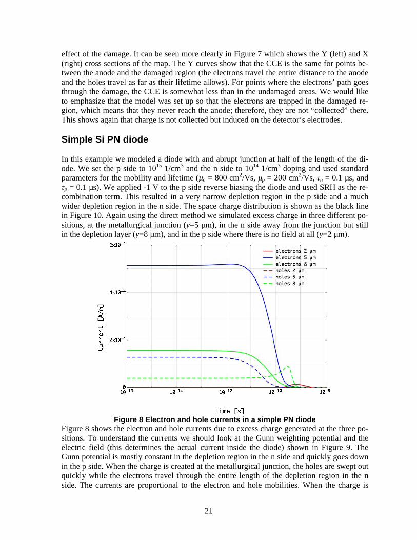
Figure 8 Electron and hole currents in a simple PN diode
Figure 8 shows the electron and hole currents due to excess charge generated at the three po-sitions. To understand the currents we should look at the Gunn weighting potential and the electric field (this determines the actual current inside the diode) shown in Figure 9. The Gunn potential is mostly constant in the depletion region in the n side and quickly goes down in the p side. When the charge is created at the metallurgical junction, the holes are swept out quickly while the electrons travel through the entire length of the depletion region in the n side. The currents are proportional to the electron and hole mobilities. When the charge is
22
created in the depletion region on the n-side (y=8 µm) the electrons are swept out quickly and the induced current is smaller than when the charge created in the middle since the electrons are travelling through a region where the electric field is low; therefore, the electron drift ve-locity is low. On the other hand, the holes travel through the depletion layer in the n and p sides, the hole current lasts an order of magnitude longer than the electron current. We should note that the peak in the hole current occurs when the holes pass the metallurgical junction where the electric field is the highest. When the charge is created in the p side where there is no field (y=2 µm), the charge has to diffuse to the junction (the Gunn weighting po-tential is zero outside of the depletion layer). Obviously, the hole current will be zero in that case and the electrons will drift through the depletion layer. But by this time the electron density will be low due to diffusion, so the current will be low. Notice again the peak in the electron current when the center of the electron distribution drifts through the junction.
Figure 9 Y components of the Gunn weighting potential (left) and the electric field
(right) of the simple PN diode
Figure 10 Simple PN diode CCE maps at various times. The black curve shows the
space charge distribution. We applied the adjoint method for this simple PN diode to calculate the CCE map. Figure 10 shows the CCE along the axis of the diode at various times. The final CCE is the curve at 10-
8 s; by this time both the electron and hole currents become zero. It is obvious from the figure
23
that we have near 100 % CCE when the charge is created in the depletion layer (there is a lit-tle drop at the junction) and the CCE decreases approximately linearly outside the depletion layer. The direct and adjoint calculations gave practically the same results for this case as shown in Figure 11. The slight differences are due to the fact that the two calculations used different grids. The direct calculation used a finer grid at the location of the charge genera-tion, while the adjoint calculation used a uniform grid except at the junction.
Figure 11 Induced charge versus time calculated by the direct (solid line) and adjoint
(dashed line) methods. Realistic PN diode The final example is a more realistic diode. The diode was made from an n-type Si substrate by diffusion where the peak of the acceptor distribution was 1017 1/cm3. A 2 µm wide ohmic contact was placed to the center of the p diffusion and -1 V was applied. The electron and hole densities with the 3 locations for which we calculated the IBIC signals are shown in Figure 12. Positions are as follows: P1 is to the left of the junction, P2 is in the p-type region about 0.5 µm from the surface, and P3 is in the n-type region about 4 µm from the surface.
Figure 12 Electron (left), hole (middle) density distribution and location of excess
change creation (right).
24
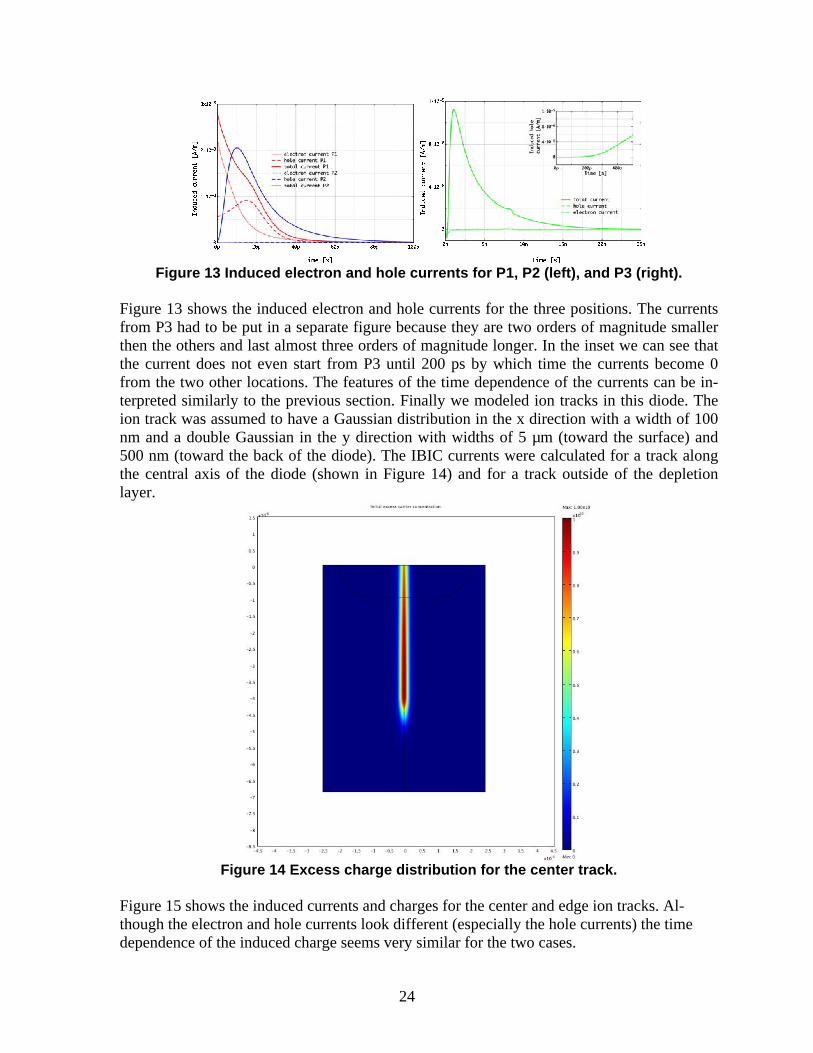
Figure 13 Induced electron and hole currents for P1, P2 (left), and P3 (right).
Figure 13 shows the induced electron and hole currents for the three positions. The currents from P3 had to be put in a separate figure because they are two orders of magnitude smaller then the others and last almost three orders of magnitude longer. In the inset we can see that the current does not even start from P3 until 200 ps by which time the currents become 0 from the two other locations. The features of the time dependence of the currents can be in-terpreted similarly to the previous section. Finally we modeled ion tracks in this diode. The ion track was assumed to have a Gaussian distribution in the x direction with a width of 100 nm and a double Gaussian in the y direction with widths of 5 µm (toward the surface) and 500 nm (toward the back of the diode). The IBIC currents were calculated for a track along the central axis of the diode (shown in Figure 14) and for a track outside of the depletion layer.
Figure 14 Excess charge distribution for the center track.
Figure 15 shows the induced currents and charges for the center and edge ion tracks. Al-though the electron and hole currents look different (especially the hole currents) the time dependence of the induced charge seems very similar for the two cases.
25
Figure 15 Induced currents (left) and charges (right) for ion tracks through the center
and the edge of the diode.
27
CONCLUSION We applied the Gunn theorem in the COMSOL Multiphysics FEM software to calculate IBIC signals from detectors and microelectronic devices. We used both the direct and the ad-joint method to calculate IBIC signals as the function of time and CCE maps. We showed through examples that the direct and the adjoint method give the same results. In the future we will extend these calculations to more complicated structures.
29
REFERENCES
1. Breese, M.B.H., et al., A review of ion beam induced charge microscopy. Nuclear
Instruments & Methods in Physics Research Section B-Beam Interactions with Materials and Atoms, 2007. 264(2): p. 345-360.
2. Shockley, W., Currents to conductors induced by a moving point charge. Journal of Applied Physics, 1938. 9(10): p. 635-636.
3. Ramo, S., Currents Induced by Electron Motion. Proceedings of I.R.E., 1939. 27: p. 584-585.
4. Gunn, J.B., A General Expression for Electrostatic Induction and its Application to Semiconductor Devices. Solid-State Electronics, 1964. 7: p. 739-742.
5. Vittone, E., Theory of ion beam induced charge measurement in semiconductor devices based on the Gunn's theorem. Nuclear Instruments & Methods in Physics Research Section B-Beam Interactions with Materials and Atoms, 2004. 219-20: p. 1043-1050.
6. Vittone, E., et al., Theory of ion beam induced charge collection in detectors based on the extended Shockley-Ramo theorem. Nuclear Instruments & Methods in Physics Research Section B-Beam Interactions with Materials and Atoms, 2000. 161: p. 446-451.
7. Ferlet-Cavrois, V., et al., Statistical Analysis of the Charge Collected in SOI and Bulk Devices Under Heavy lon and Proton Irradiation—Implications for Digital SETs. IEEE Transaction on Nuclear Science, 2006. 53(6): p. 3242-3252.
8. Ferlet-Cavrois, V., et al., Charge collection by capacitive influence through isolation oxides. IEEE Transactions on Nuclear Science, 2003. 50(6): p. 2208-2218.
9. Ohshima, T., et al. Change in Ion Beam Induced Current from Si Metal-Oxide-Semiconductor Capacitors after Gamma-Ray Irradiation. 2008. Ft Worth, TX.
10. Schwank, J.R., et al., Charge collection in SOI capacitors and circuits and its effect on SEU hardness. IEEE Transactions on Nuclear Science, 2002. 49(6): p. 2937-2947.
11. Schwank, J.R., et al., Analysis of heavy-ion induced charge collection mechanisms in SOI circuits. Solid-State Electronics, 2004. 48(6): p. 1027-1044.
12. Vizkelethy, G., D.K. Brice, and B.L. Doyle, Heavy ion beam induced current/charge (IBIC) through insulating oxides. Nuclear Instruments & Methods in Physics Research Section B-Beam Interactions with Materials and Atoms, 2006. 249: p. 204-208.
13. Vizkelethy, G., D.K. Brice, and B.L. Doyle, The theory of ion beam induced charge in metal-oxide-semiconductor structures. Journal of Applied Physics, 2007. 101(7).
14. Vizkelethy, G., et al., Anomalous charge collection from silicon-on-insulator structures. Nuclear Instruments & Methods in Physics Research Section B-Beam Interactions with Materials and Atoms, 2003. 210: p. 211-215.
15. Prettyman, T.H. Theoretical framework for mapping pulse shapes in semiconductor radiation detectors. 1998. Jerusalem, Israel.
16. Prettyman, T.H. Method for mapping charge pulses in semiconductor radiation detectors. 1998. Ann Arbor, Michigan.
17. Vittone, E., Private communication. 2009. 18. Doyle, B.L., G. Vizkelethy, and D.S. Walsh, Ion beam induced charge collection
(IBICC) studies of cadmium zinc telluride (CZT) radiation detectors. Nuclear Instruments & Methods in Physics Research Section B-Beam Interactions with Materials and Atoms, 2000. 161: p. 457-461.
31
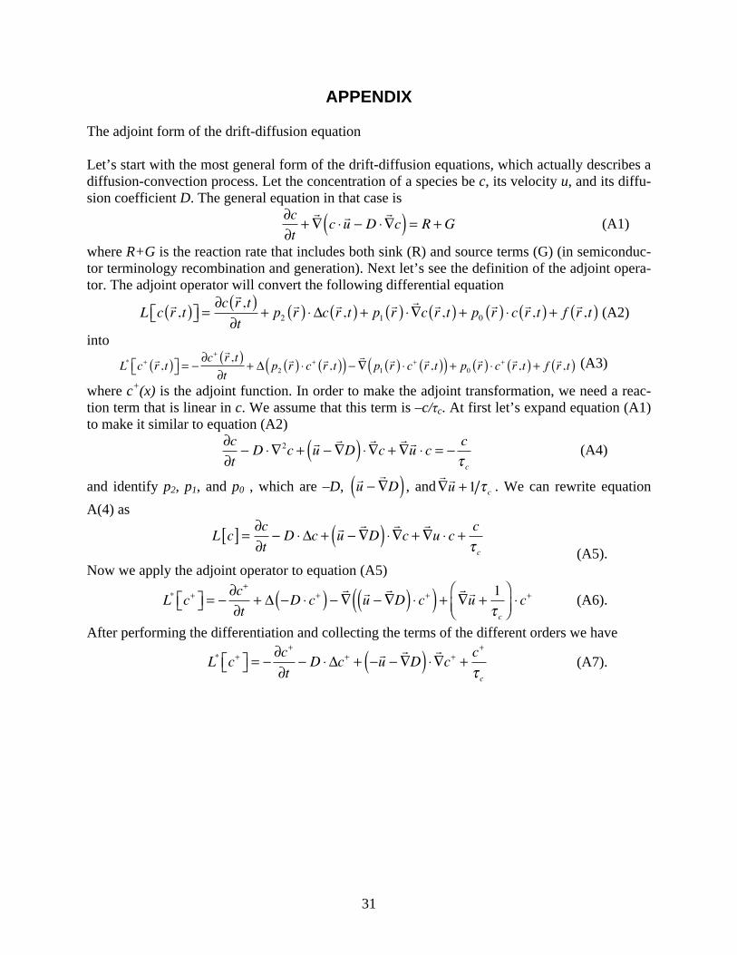
APPENDIX The adjoint form of the drift-diffusion equation Let’s start with the most general form of the drift-diffusion equations, which actually describes a diffusion-convection process. Let the concentration of a species be c, its velocity u, and its diffu-sion coefficient D. The general equation in that case is
∂c∂t
+∇ c ⋅ u − D ⋅
∇c( ) = R +G (A1)
where R+G is the reaction rate that includes both sink (R) and source terms (G) (in semiconduc-tor terminology recombination and generation). Next let’s see the definition of the adjoint opera-tor. The adjoint operator will convert the following differential equation
L c r ,t( )⎡⎣ ⎤⎦ =
∂c r ,t( )∂t
+ p2r( ) ⋅ Δc r ,t( ) + p1
r( ) ⋅∇c r ,t( ) + p0
r( ) ⋅ c r ,t( ) + f r ,t( ) (A2)
into
L* c+ r ,t( )⎡⎣ ⎤⎦ = −
∂c+ r ,t( )∂t
+ Δ p2r( ) ⋅ c+ r ,t( )( ) − ∇ p1
r( ) ⋅ c+ r ,t( )( ) + p0 r( ) ⋅ c+ r ,t( ) + f r ,t( ) (A3)
where c+(x) is the adjoint function. In order to make the adjoint transformation, we need a reac-tion term that is linear in c. We assume that this term is –c/τc. At first let’s expand equation (A1) to make it similar to equation (A2)
∂c∂t
− D ⋅∇2c + u −∇D( ) ⋅ ∇c + ∇u ⋅ c = −
cτ c
(A4)
and identify p2, p1, and p0 , which are –D, u −∇D( ) , and
∇u +1 τ c . We can rewrite equation
A(4) as
L c[ ] = ∂c
∂t− D ⋅ Δc + u −
∇D( ) ⋅ ∇c + ∇u ⋅ c + c
τ c (A5). Now we apply the adjoint operator to equation (A5)
L* c+⎡⎣ ⎤⎦ = −
∂c+
∂t+ Δ −D ⋅ c+( ) − ∇ u −
∇D( ) ⋅ c+( ) +
∇u + 1τ c
⎛⎝⎜
⎞⎠⎟⋅ c+ (A6).
After performing the differentiation and collecting the terms of the different orders we have