All 3 phase Fluxgate sensor outputs are summed together and given as inputs to these comparators
VTH
VTH
VTL
VTLOvercurrentIndication
Earth FaultIndication
Optional SPI Connection for External Motor Controller
x 4 5V
+6V DC input
x 2
TIDA - 00208
DC BUS_P
DC BUS_M
DC Link Current
R Y B
x 3
Piccolo�F28027
TPS7A4700 REF5025+ OPA322
TLV70033
REF2033
TLC372
TLC372
MOTOR
OPA4322
ADS7853
TI DesignsSingle-Ended Signal Conditioning Circuit for Current andVoltage Measurement Using Fluxgate Sensors
TI Designs Design FeaturesTI Designs provide the foundation that you need • Designed to Measure All 3-Phase Motor Currentsincluding methodology, testing and design files to Along with DC-Link Current Through 6-A Fluxgatequickly evaluate and customize the system. TI Designs Sensor (Scalable up to 50 A)help you accelerate your time to market. • Single-Ended Signal Conditioning Circuit to
Interface Fluxgate Sensors With Single-EndedDesign Resources ADCs• Two Onboard 14-Bit Dual Channel SimultaneousTool Folder Containing Design FilesTIDA-00208
Sampling SAR ADCs With 4-Wire SPI to InterfaceOPA4322 Product Folder With External Motor ControllersADS7853 Product Folder
• Provision to Measure Current and Voltage ThroughADS7253 Product FolderInternal ADCs of TI's Piccolo™ ControllerTPS7A4700 Product FolderTMS320F28027TLV70033 Product Folder
• < 0.1% DC Accuracy of Signal Conditioning CircuitREF5025 Product FolderREF2033 Product Folder • Overload and Earth Fault Protections for Each
Channels With <100-ns Sensing DelaysTLC372 Product FolderOPA322 Product Folder • Provision to Interface the Signal ConditioningLAUNCHXL-F28027 Tool Folder Circuit With External ADC
Featured ApplicationsASK Our E2E Experts • AC Variable Speed and Servo Motor DrivesWEBENCH® Calculator Tools
• Static Converters• DC Motor Drives• UPS Systems• Solar Inverters• Power Supplies for Welding Applications
All trademarks are the property of their respective owners.
1TIDU583–October 2014 Single-Ended Signal Conditioning Circuit for Current and VoltageMeasurement Using Fluxgate SensorsSubmit Documentation Feedback
B) Current measurement in the bottom side emitter path of each half-bridge
C) Current measurement in the output phases
3~
B
System Description www.ti.com
An IMPORTANT NOTICE at the end of this TI reference design addresses authorized use, intellectual property matters and otherimportant disclaimers and information.
1 System DescriptionCurrent measurement is an inherent part of any inverter-driven application. One important reason formeasuring the motor current is to control algorithm. Vector control and direct torque control require currentsensing for control purposes. Approaches for sensorless control require the motor current measurement toprovide accurate control with low cost and complexity. Information of motor parameters is important forseveral control schemes. Stator current measurement is used for the estimation of these parameters.Motor current information is also required to detect the motor’s insulation condition. Electrical insulation isthe most critical component for operating electrical motors. Stator insulation failure during motor operationcan lead to motor failure, resulting in a costly outage.
Another important phenomenon is protection from hardware overload and earth fault conditions. Typically,these conditions occur when the current exceeds the limit of 200% or 300% of its nominal current.Derating must be taken into account when using the drive in different conditions. Ambient temperature orother environmental conditions such as dust or humidity are unknown, especially when a drive is notinstalled by the end-user but the machine manufacturer. The end user must identify all derating factors toreach a reliable solution.
Above the drive-designed ambient temperature, drives can usually operate when the maximum outputcurrent is derated according to the user’s manual of the drive. The switching frequency also playsimportant role. The higher the switching frequency of the drive is, the more the power semiconductorsgenerate heat losses. Therefore, the drive output current is derated when increasing the switchingfrequency, which applies to nominal current, overload current, and maximum instantaneous current.
The motor current can be measured at different points in the inverter. Figure 1 shows the overview ofusual measurement locations, considering a 3-phase inverter for a motor control application:
Figure 1. Typical Measuring Locations for Current Measurement in Motor Drives
2 Single-Ended Signal Conditioning Circuit for Current and Voltage TIDU583–October 2014Measurement Using Fluxgate Sensors Submit Documentation Feedback
From Figure 1, the least expensive variant of current measurement (A) is often used for applications in thelower power range. Typically, the current measurement is done on DC-MINUS bus, because this may bethe reference potential of the microcontroller (MCU) and is therefore not necessary to isolate the signal.Another alternative location of current measurement, found particularly in the low-to-medium power rangeis variant B. In this case, the current is measured at the emitter of the bottom IGBT of each arm in a 3-phase inverter. The end user can also dispense with third current measurement as this can be derived bycalculation based on the two measured current signals. The advantage of this measurement method issimilar to that of variant a, in that the negative section of the DC-bus can be taken as the commonreference potential. However, the disadvantage is the increased stray inductance. In high dynamic drivesand high-power applications, current is usually measured in the output phases of the inverter (variant C inFigure 1). The third current sensor is not necessary in this case either.
The design TIDA-00208 is predominantly intended for current measurement using fluxgate sensors in ACmotor drives, but the design can also be used for DC drives. The objective of this design is to provide asolution for single-ended signal conditioning circuit along with SAR analog-to-digital converters (ADCs) tomeasure motor current using fluxgate sensors, typically available from companies like LEM Technologiesand VACUUMSCHMELZE. Designs commonly use single-ended ADCs integrated inside the controller forcurrent measurement for industrial motor drives. This design overcomes inaccuracies by using low-costfront-end op-amps with proper filtering. This design also shows the front-end interfacing with the Piccoloseries of MCUs (consisting of single-ended input ADCs) from Texas Instruments (TI).
The signal conditioning circuit for fluxgate current sensors is required for the following reasons:• Fluxgate sensors have inherent noise at 450 kHz / 900kHz because of the internal oscillator and
switching, so proper filtering is required.• Typical fluxgate sensors have a reference signal on REF pin (always at 2.5 V) and signal output
available on the OUT pin (±0.625 V riding on a 2.5-V reference). The output voltage of fluxgatesensors may not match the input range of ADCs (external or internal to the controller). In this scenario,level shifting may be required.
• Fluxgate sensors can measure up to 300% of their nominal rating. It is important to detect the overloadcondition and protect the drive.
• For a fluxgate sensor with nominal current (In) of 6 A with 300% of nominal current rating, the signalstrength can vary from 0.625 V [2.5 – (3 × 0.625)] to 4.375 V [2.5 + (3 × 0.625)]. However, the ADCsintegrated into microcontrollers can take 0 to 3.3 V, so level shifting is required.
• If using single-ended ADC inside Piccolo controllers, the common-mode voltage needs to be shiftedfrom 2.5 V to 1.65 V, unlike the external ADCs.
2 Design Requirements• To measure a 3-phase motor current and DC-Link current in a variable speed drive using fluxgate
sensor (up to 6 A)• Signal conditioning circuit with 0.1% accuracy to interface with a single-ended SAR ADC• Simultaneous sampling of all current channels• Hardware overload detection within < 100 ns• Hardware earth fault detection within < 100 ns
3TIDU583–October 2014 Single-Ended Signal Conditioning Circuit for Current and VoltageMeasurement Using Fluxgate SensorsSubmit Documentation Feedback
All 3 phase Fluxgate sensor outputs are summed together and given as inputs to these comparators
VTH
VTH
VTL
VTLOvercurrentIndication
Earth FaultIndication
Optional SPI Connection for External Motor Controller
x 4 5V
+6V DC input
x 2
TIDA - 00208
DC BUS_P
DC BUS_M
DC Link Current
R Y B
x 3
Piccolo�F28027
TPS7A4700 REF5025+ OPA322
TLV70033
REF2033
TLC372
TLC372
MOTOR
OPA4322
ADS7853
Block Diagram www.ti.com
3 Block DiagramThe system block diagram is shown in Figure 2. This design uses four fluxgate current sensors: three forthe motor phase currents and one for measuring the current flowing through the DC-Link. Each of thesensors is interfaced with the quad low-noise op-amp OPA4322. The four outputs of OPA4322 are:1. Connected to the onboard 14-bit SAR ADCs (ADS7853), the digital output of which is taken out on a
connector to interface with external motor controllers or processors2. Connected to the 40-pin connector to interface with the internal ADC of Piccolo TMS320F28027
To provide protection against overcurrent fault condition, each of the phases is provided with two fastresponding comparators, the TLC372 (one for detection of overcurrent in a positive half-cycle and one fordetection of overcurrent in a negative half-cycle). For ground fault detection, the output signals comingfrom each of the phases are combined together and compared against references using two TLC372s.Both protection circuits have a response time of less than 100 nanoseconds.
The entire board receives power from the 6-V DC power supply available on most of the industrial motordrives. The 6-V DC input is step-downed by a high-precision, low-noise low-dropout regulator (LDO)TPS7A4700 to generate 5 V. (TPS7A4700 has an input voltage range up to 36 V, so it can also be usedin case a 15-V or 24-V supply is available). The 5 V is used to power the operational amplifiers (op-amps),onboard ADCs, and the fluxgate current sensors. For a digital supply, the low-cost LDO TLV70033 is usedfor 5-V to 3.3-V conversion. When used with 5-V ADCs, the output of op-amps should be biased at 2.5 Vwhereas when used with internal ADC of the Piccolo controller, the output should be biased at 1.65 V. The2.5-V reference is generated using the REF5025 and OPA322 (used as buffer for reference). TheREF2033 is used to generate reference voltage of 1.65 V and 3.3 V.
Figure 2. System Block Diagram
4 Single-Ended Signal Conditioning Circuit for Current and Voltage TIDU583–October 2014Measurement Using Fluxgate Sensors Submit Documentation Feedback
4 Highlighted ProductsThis reference design features the following devices from TI:• OPA4322: Low-noise, 1.8-V, RRI/O, CMOS op-amp• ADS7253 and ADS7853: Dual, high-speed, 12-bit and 14-bit, simultaneous-sampling, SAR ADCs• TPS7A4700: 1-A, low noise (4.17μVRMS), high-voltage LDO• TLV70033: 200-mA, low IQ, LDO• REF5025 - Low-noise, very low-drift, precision voltage reference• OPA322 - Low-noise, 1.8-V RRIO, CMOS om-amp with shutdown• REF2033: Low-drift, low-power, dual-output VREF and VREF / 2 voltage reference• TLC372: Dual general purpose LinCMOS™ differential comparator
For more information on each of these devices, see their respective product folders at www.ti.com or clickon the links for the product folders in Design Resources.
5TIDU583–October 2014 Single-Ended Signal Conditioning Circuit for Current and VoltageMeasurement Using Fluxgate SensorsSubmit Documentation Feedback
5.1 Open-Loop and Close-Loop Fluxgate SensorsThe operating principle of open-loop current transducers is shown in Figure 3 (taken from LEMTechnologies' voltage transducer catalogue). The magnetic flux created by the primary current IP isconcentrated in a magnetic circuit and measured in the air gap using a fluxgate device. The output fromthe fluxgate device is then signal conditioned to provide an exact representation of the primary current atthe output.
Figure 3. Open-Loop Fluxgate Sensor
On the other hand, the operating principle of a close-loop fluxgate sensor is that of a current transformerequipped with a magnetic sensing element, which senses the flux density in the core. As shown inFigure 4, the output of the field sensing element is used as the error signal in a control loop driving acompensating current through the secondary winding of the transformer. At low frequencies, the controlloop maintains the flux through the core near zero. As the frequency rises, an increasingly large fraction ofthe compensating current is due to the operation in transformer mode. The secondary current is thereforethe image of the primary current. In a voltage output transducer, the compensating current is converted toa voltage through a precision resistor and made available at the output of a buffer amplifier.
Figure 4. Close-Loop Fluxgate Sensor
6 Single-Ended Signal Conditioning Circuit for Current and Voltage TIDU583–October 2014Measurement Using Fluxgate Sensors Submit Documentation Feedback
5.2 Details of Fluxgate Sensor CKSR 6-NP From LEM TechnologiesSelecting the right transducer is often a trade-off between several parameters: accuracy, frequencyresponse, weight, size, costs, and so on. The CKSR 6-NP is a close-loop fluxgate sensor from LEMTechnologies. The CKSR 6-NP typically measures current (DC, AC, or pulsed) with galvanic separationbetween the primary and secondary circuit. The internal structure of CKSR 6-NP is shown in Figure 5.
Figure 5. Internal Structure of CKSR 6-NP
The CKSR 6-NP can do bipolar measurements with a single unipolar 5-V power supply. The device canprovide its internal voltage reference on an external pin (VREF) or receive an external voltage reference toshare it with MCUs or ADCs. The output signal is available on the OUT pin, which is an amplified voltagesignal proportional to the primary current. In a single-supply voltage, the output signal varies around anon-zero reference. In CKSR 6-NP, the output signal rides over a 2.5-V reference. The output voltage isproportional to the nominal primary current as shown in Equation 1.
where• VOUT is output voltage• I is the primary current• In is nominal primary current (for example, In = 6 A for CKSR 6-NP) (1)
Close-loop fluxgate transducers provide excellent accuracy at 25°C, generally below 1% of the nominalrange, and a reduced error over the specified temperature range (–40°C to 105°C). Table 1 shows theaccuracy data for CKSR 6-NP (taken from its datasheet).
Table 1. Accuracy of CKSR 6-NP
PARAMETER SYMBOL UNIT MIN TYP MAXOverall accuracy XG % of IPN 1.7
Overall accuracy at TA = 85°C (105°C) XG % of IPN 2.2 (2.4)Accuracy X % of IPN 0.8
Accuracy at TA = 85°C (105°C) X % of IPN 1.4 (1.6)
7TIDU583–October 2014 Single-Ended Signal Conditioning Circuit for Current and VoltageMeasurement Using Fluxgate SensorsSubmit Documentation Feedback
6 Overcurrent and Earth Fault ProtectionContemporary state-of-the-art inverters are equipped with full IGBT protection, including overcurrent andearth fault protection. An overcurrent condition is one of the fatal drive faults that could destroy IGBTdevices in a motor drive system. IGBT overcurrent conditions fall into three categories: ground fault,line-to-line short, and shoot-through.
Table 2. Overcurrent Conditions and Possible Causes
OVERCURRENT CONDITION POTENTIAL CAUSEGround fault Motor insulation breakdown to ground
Mis-wiring, motor leads short, motor phase-to-phase insulationLine-to-line short breakdownShoot-through False IGBT turn-on
Table 2 lists overcurrent conditions and their potential causes. When considering an IGBT overcurrentprotection scheme, evaluate two important factors. The first factor is what type of overcurrent protectionthe system must provide and how the system can shut down. The second factor is the control architecture.Control architecture significantly influences the method and implementation of the overcurrent protection.Protection of IGBT devices is normally implemented in the hardware circuit. However, the circuitimplementation and the type of overcurrent-sensing device vary depending on which overcurrent conditionis being addressed.
This design implements the overcurrent protection using two comparators for each phase. The twothresholds are derived from the output voltage coming from fluxgate sensors (one for the positive cycleand one for the negative cycle). On the other hand, the earth fault protection is implemented by adding thethree signals coming from current sensors connected in each phase and compared against two thresholds(one for the positive cycle and one for the negative cycle).
The total propagation delay of shutdown also is important. The current sensor itself has some delay, whichincludes delay for the sensing mechanism and its own response time. Therefore, no matter how theprotection circuit is implemented, this delay time must be added to the circuit delay to meet the IGBTshort-circuit duration time.
8 Single-Ended Signal Conditioning Circuit for Current and Voltage TIDU583–October 2014Measurement Using Fluxgate Sensors Submit Documentation Feedback
7.1 Selection of ADC• Input voltage range: CKSR 6-NP fluxgate sensor provides a 2.5-V reference output and an output
voltage proportional to primary current riding on a 2.5-V reference signal. The output voltagecorresponding to the measured current is given by VREF – VOUT. This differential signal can go up to300% of its nominal output (that is, ±0.625 × 3 = ±1.875 V).
• Number of channels: The three phases (R, Y, and B) and DC-Link current measurement require fourchannels. It is better to have four ADCs that can be simultaneously sampled.
• Simultaneous sampling: For optimal 3-phase motor control, it is important to take simultaneous currentmeasurements for each of the phases.
• Sampling speed: A typical industrial motor drive application uses a sampling frequency of 100 to 250kSPS, so the minimum sampling frequency required for the selected ADC is 300 kSPS.
• Number of bits (resolution): Generally, 12 to 14 bits of resolution is enough for an industrial motor driveusing fluxgate sensors.
• Supply voltage: Since the CKSR 6-NP has an operating voltage range from 4.75 to 5.25 V, use anADC with a supply voltage of 5 V.
• Reference requirement: Have internal as well external reference options on hand.
ADS7253 and ADS7853 are suitable devices for the mentioned criteria. The features of ADS7253 andADS7853 are as follows:• Pin compatible family: 12 to 14 bits• Simultaneous sampling of two channels (If the /CS signal of two ADS7x53 devices combine, all four
ADCs — two in each ADS7x53 — can be sampled simultaneously).• Sampling speed: 1 MSPS• Single-ended and pseudo-differential inputs• Excellent DC/AC performance• Dual, programmable, buffered 2.5-V internal reference for gain calibration• Extended temperature range: –40°C to 125°C
9TIDU583–October 2014 Single-Ended Signal Conditioning Circuit for Current and VoltageMeasurement Using Fluxgate SensorsSubmit Documentation Feedback
7.2 Selection of Operational AmplifierThe op-amp is a critical piece of the analog signal chain and can often have a dramatic impact on theperformance of the entire signal chain. The primary functions of this op-amp are:1. To buffer the inputs coming from the sensor2. To amplify the low level input signals coming from the sensor3. To provide the desired common-mode voltage at the output
Table 3 gives a comprehensive list of the factors that need to be considered in determining the choice ofthe op-amp.
Table 3. Selection Considerations for the Op-Amp
REQUIREMENT BENEFITMinimizing this reduces input loading on sensor, and minimizesHigh input impedance input current offsets on input resistors.Minimizing this reduces the amount of current noise thatInput current noise becomes converted to voltage noise on input resistors.
Voltage noise Minimizing this improves the overall signal-to-noise ratio.Maximizing this reduces the amount of input offset changes dueCMRR versus frequency to high dv/dt at the inverter output.Minimizing this reduces the amount that the total unadjustedVoltage offset drift error changes at the output of the op-amp.Designing a single-supply amplifier simplifies the system supply
Single-supply operation requirements, which usually correlate with a lower powerarchitecture.A rail-to-rail input can help to interface sensors that have largeInput type input swings.With a rail-to-rail output configuration, the amplified input signal
Output type can reach the supply voltage and can use the FS range of ADCin a more successful way.
This reference design uses OPA4322 as front-end amplifier for ADC. The OPA4322 is a quad-channelCMOS op-amp featuring low noise and rail-to-rail I/Os optimized for single-supply applications.
7.3 Selection of External Voltage ReferencesTIDA-00208 uses ADS7253, which has an external reference voltage range from 2.4 V to AVDD (or 5 V)as shown in Table 4 (taken from the ADS7253 datasheet).
Table 4. Voltage Reference Input Limits
PARAMETER TEST CONDITIONS MIN TYP MAX UNIT±VREF range 2.4 2.5 AVDD V
VREF reference voltage (input) AVDD /2 × VREF range 2.4 2.5 V2
The design needs an external reference IC that can provide 2.5 V. The REF5025, selected for thisreference, is a low-noise, low-drift, very high-precision voltage reference.
On the other hand, the internal ADC of a controller can take a maximum voltage of 2.5 V on the analoginput pins. For signals coming to the inputs of internal ADCs, the common-mode voltages must be at mid-scale to bias the input bipolar signals. The REF2033 can provide two voltages: 1.65 V and 3.3 V.
10 Single-Ended Signal Conditioning Circuit for Current and Voltage TIDU583–October 2014Measurement Using Fluxgate Sensors Submit Documentation Feedback
7.4 Selection of ComparatorA typical industrial drive needs to have overcurrent and earth fault protection to operate within 300nanoseconds. To reach this goal, the following comparators are compared and TLC372 is selected. TheTLC372 has a 200-nanosecond response time. Table 5 shows the comparison chart.
Table 5. Comparison Chart for Comparator Selection
PARAMETER LM293 LM293A TLC372 TLV1702 LMV7235 LM6511 TLV1391No. of 2 2 2 2 1 1 1ChannelsSupply voltage 2 2 3 2.2 2.7 2.5 2(min) in VoltsSupply voltage 36 36 16 36 5.5 30 7(max) in VoltsT(RESP) low- 1.3 1.3 0.2 0.78 0.075 0.18 0.7to-high (in μS)
Open- Open- Open- Open-Open-drain,Output type collector, collector, collector, Open-collector Open-collector collector,Push-pullOpen Drain Open Drain Open Drain Open DrainInput offsetvoltage (in 5 2 5 0.3 6 8 9mV) - MaxInput offsetcurrent (in nA) 50 50 0.001 0.5 200 200 150- MaxInput biascurrent (in nA) 250 250 0.03 20 400 50 400- MaxSupply current 1 1 0.3 ?? 0.1 5 0.175(in mA) - Max
SOIC-8, SOIC-8, SOIC-8,Packages MSOP8-, SOT-23, SC-VSSOP-8, VSSOP-8, TSSOP-8, SOIC-8 SOT-23available QFN-8 70PDIP-8 PDIP-8 PDIP-8, SO-8Temperature –25 to 85 –25 to 85 –40 to 125 –40 to 125 –40 to 85 –40 to 85 –40 to 85(in °C)
7.5 Selection of Power Devices: Voltage RegulatorsThe entire board is powered using the 6-V DC power supply available on most of the industrial motordrives. The drive can also have 24-V or 15-V supplies available. To step down the 6-V DC input togenerate 5 V, the board requires a high-precision, low-noise LDO. The 5-V is used to power op-amps,onboard ADCs as well as the fluxgate current sensors, so the total current output requirement from theLDO is at least 500 mA.
The TPS7A47 is a family of positive voltage (36 V), ultra low-noise (4 μVRMS) LDOs capable of sourcing a1-A load. The TPS7A4700 output voltages are user-programmable (up to 20.5 V) using a printed circuitboard (PCB) layout without the need of external resistors or feed-forward capacitors, which reduces theoverall component count. The TPS7A47 is designed with bipolar technology primarily for high-accuracy,high-precision instrumentation applications where clean voltage rails are critical to maximize systemperformance. This feature makes the device ideal for powering op-amps, ADCs, digital-to-analogconverters (DACs), and other high-performance analog circuitry. (TPS7A4700 has an input voltage rangeup to 36 V, so the device can also be used in case a 15-V or 24-V supply is available). The digital supplyrequires a low-cost LDO to convert the 5 V to 3.3 V with a <200-mA output current capability. TheTLV70033 is a 3-pin, low-cost LDO that can provide the 200-mA current to convert the 5 V to 3.3 V.
11TIDU583–October 2014 Single-Ended Signal Conditioning Circuit for Current and VoltageMeasurement Using Fluxgate SensorsSubmit Documentation Feedback
8.1 Decoupling for Fluxgate Current SensorAs per the CKSR 6-NP datasheet, the internal fluxgate oscillator draws current pulses of up to 30 mA at arate of 900 kHz. A significant 900-kHz voltage ripple on the supply pin (Vc) can indicate a power supplywith high impedance. At these frequencies, the power supply rejection ratio is low, and the ripple mayappear on the transducer output Vout and reference Vref. The transducer has internal decouplingcapacitors, but in the case of a power supply with high impedance, it is better to use local decoupling(100 nF or more, located close to the transducer).
In this design, the fluxgate sensor is decoupled using the 1-µF ceramic capacitor (as shown in Figure 6).The capacitor is placed very close to the sensor in the layout.
Figure 6. CKSR 6-NP with Capacitor Decoupling on Supply Pin
8.2 Designing the ADC Input StageConverting analog-to-digital signals requires sampling an input signal at a constant rate. Any higherfrequency content in the input signal beyond half the sampling frequency is digitized and folded back intothe low-frequency spectrum. This process is called aliasing. Therefore, an analog anti-aliasing filter mustremove the harmonic content from the input signal before being sampled by the ADC. An anti-aliasingfilter is designed as a low-pass RC filter, for which the 3-dB bandwidth is optimized based on specificapplication requirements. A high-bandwidth filter is required to allow accurately settling the signal at theADC inputs during the small acquisition time window. For AC signals, the filter bandwidth should be keptlow to band-limit the noise fed into the ADC input, thereby increasing the signal-to-noise ratio (SNR) of thesystem. The datasheet of ADS7253 suggests the component values for anti-aliasing filter as shown inFigure 7:
Figure 7. Anti-Aliasing Filter for ADS7x53
The cut-off frequency of anti-aliasing filter is calculated using Equation 2.
(2)
12 Single-Ended Signal Conditioning Circuit for Current and Voltage TIDU583–October 2014Measurement Using Fluxgate Sensors Submit Documentation Feedback
Designing the input stage is a two-step optimization process:1. Select a noise rejection input capacitor that charges the sample-hold capacitor (CSH).2. Identify an op-amp that can consume low power and recharge the input capacitor.
A filter capacitor, CFLT, which connects across the ADC inputs and filters the noise from the front-end drivecircuitry, reduces the sampling charge injection and provides a charge bucket to quickly charge theinternal sample-and-hold capacitors during the acquisition process. The noise reduction filter blockconsists of a capacitor, CFLT, which is added between the two input pins as shown in Figure 8. This blockhelps minimize noise by attenuating the kick-back noise from the ADC and also by band-limiting thebroadband noise of the op-amp.
Figure 8. Input Capacitor CFLT for Attenuating Noise
This filter capacitor acts as a charge reservoir by providing the charges to CSH during acquisition time. Theop-amp delivers charges to the capacitor to bring it up to the input voltage V as shown in Figure 9. Thiscapacitor must be large enough to charge or discharge the sample-hold capacitor during acquisition timeand retain 95% of its initial voltage.
Figure 9. Filter Capacitor Delivering Charges to CSH
13TIDU583–October 2014 Single-Ended Signal Conditioning Circuit for Current and VoltageMeasurement Using Fluxgate SensorsSubmit Documentation Feedback
The sampling capacitor inside ADS7x53 has a typical value of 40 pF. When the input is at its maximum,CSH has to be charged to 2xVREF during the sampling time. The corresponding charge needed isapproximately 200 pC (40 pF × 5 V). While delivering 200 pC to CSH, the voltage across this capacitorshould not drop below 5% of its initial voltage, which is VREF to keep the op-amp in its linear operatingregion (no slew).
As a rule of thumb, the value of this capacitor should be at least 20 times the specified value of the ADCsampling capacitance. For these devices, the input sampling capacitance is equal to 40 pF. Therefore, thevalue of CFLT should be greater than 800 pF. Note that driving capacitive loads can degrade the phasemargin of the input amplifiers, which makes the amplifier marginally unstable. To avoid amplifier stabilityissues, series isolation resistors (RFLT) are used at the output of the amplifiers. A higher value of RFLT ishelpful from the amplifier stability perspective but adds distortion as a result of interactions with thenonlinear input impedance of the ADC. Distortion increases with source impedance, input signalfrequency, and input signal amplitude. Therefore, the selection of RFLT requires balancing the stability anddistortion of the design. For these devices, TI recommends limiting the value of RFLT to a maximum of22 Ω to avoid any significant degradation in linearity performance. The tolerance of the selected resistorscan be chosen as 1%.
TIDA-00208 uses CFLT = 0.01 μF and RFLT = 10 Ω, with the cut-off frequency of 79.58 kHz.
The flicker and broadband noise introduced by the op-amp (or FDA) can be verified using Equation 3:
(3)
14 Single-Ended Signal Conditioning Circuit for Current and Voltage TIDU583–October 2014Measurement Using Fluxgate Sensors Submit Documentation Feedback
8.3 Designing the Amplifier StageFigure 10 shows the OPA4322 section. As mentioned earlier, TIDA-00208 has four sensors on board,which means the design requires four amplifiers. The OPA4322 is a quad op-amp, and each channel inOPA4322 is used for one fluxgate sensor.
Important observations from Figure 10 are:• Single-supply operation: The OPA4322 is powered through 5 V coming out of TPS7A4700 (as
explained in Section 8.6). One bypass capacitor with a value of 0.1 μF is placed very close to theAVDD pin of OPA4322.
• Output common-mode setting: The non-inverting pin of the op-amp is supplied with 2.5 V (coming fromVREF_BUF or the sensor REF output) in case the pin interfaces with an external ADC. But when theinternal ADC of the Piccolo controller is used, the common-mode voltage needs to be 1.65 V. In thatcase, the external voltage on non-inverting pin of op-amp is supplied through 1.65 V (coming fromREF2033 REF/2).
• Input signal filtering: The fluxgate sensors have an inherent noise due to their internal structure. Bothinputs of OPA4322 use a low-pass filter. The design of filters is explained in Section 8.4.
• Selection of gain:– When used with the external ADC, the output can have a common-mode voltage of 2.5 V and the
full-scale range of the ADC can be 5 V. The fluxgate sensors can work up to 300% of their nominalcurrent range, which means the signal must have a gain to go from 1.875 to 2.5 V at 300% of theoperating current. This signal gives a gain of 1.33.
– When used with internal ADC of controller, the output can have a common-mode voltage of 1.65 Vand the full-scale range of the ADC can be 3.3 V. The fluxgate sensors can work up to 300% oftheir nominal current range, which means the signal must have a gain to go from 1.875 to 1.65 V at300% of the operating current. This signal gives a gain of 0.88. If the current measurementrequirement is only up to 200% or 250%, a gain of 1 can be used.
• Selection of components: The 0.1-μF caps in the feedback helps to reduce overall noise of the system.One important thing to note that the resistors also have their internal noise. The resistor noise dependson the value of resistor. Select the input and feedback resistor values in some kΩ (preferably < 5 kΩ)to reduce the effect of noise from resistors.
Figure 10. OPA4322 Interface Between Sensor and ADC
15TIDU583–October 2014 Single-Ended Signal Conditioning Circuit for Current and VoltageMeasurement Using Fluxgate SensorsSubmit Documentation Feedback
8.4 Noise Filtering for Fluxgate Current SensorFluxgates have an inherent noise (450 kHz / 900 kHz) at their output that needs filtering. A low-pass filteris designed with a cut-off frequency of 20 kHz using TI’s FilterPro™ software as shown in Figure 11.
Figure 11. Low-Pass Filter Design Simulation Using FilterPro
16 Single-Ended Signal Conditioning Circuit for Current and Voltage TIDU583–October 2014Measurement Using Fluxgate Sensors Submit Documentation Feedback
8.5 Designing the Reference Circuit for ADCAn ADC is as good as its reference because ADCs compare an input to a known reference and its binaryscaled weights to estimate an equivalent digital code. An accurate digital conversion of the input signalrequires a highly accurate, low-drift, low-noise reference. The reference should also support the dynamiccharge requirements without affecting the noise and linearity performance of the device. An ideal ADC isone that gives the same digital code for a given input. For a capacitor-based ADC reference input, theload at the reference pin spikes out every time a bit value is estimated. Not only does reference currenttransient multiple times within a conversion cycle, but also the magnitude of the transient current varybetween the conversions. A noisy reference shows up as a variation of code out at the output of the ADCfor a fixed input. A noisy reference also degrades the linearity, THD, and SNR.
Figure 12. Reference Driver Circuit
As shown in Figure 12, designing the reference drive circuitry is a four-step optimization process thatinvolves1. identifying a reference that is suitable for the application2. designing a filter that limits the broadband noise from the reference3. estimating the capacitor value needed to provide the reference drive current4. identifying an op-amp that is suitable for low power that can recharge the capacitor
17TIDU583–October 2014 Single-Ended Signal Conditioning Circuit for Current and VoltageMeasurement Using Fluxgate SensorsSubmit Documentation Feedback
A reference can introduce two types of noise: flicker noise and broadband noise. Flicker noise is the noisedominant at low frequencies and broadband noise dominates at high frequencies. The broadband noise, inparticular, can be of the order of hundreds of microvolts and can easily exceed the tens of microvolts ofRMS noise of the converter. Typically, flicker noise is specified on the datasheet as peak-to-peak noise upto 10 Hz. This noise has to be scaled down by a factor of 6.6 to convert it into RMS noise. On the otherhand, the density of broadband spectral noise may not be specified on the datasheet. For a band-gapreference, the density is 0.1 μVRMS/√Hz to 10 μVRMS/√Hz in magnitude and is inversely proportional to thesquare root of the quiescent current of the reference. If the reference is not specified, Equation 4 gives agood approximation:
(4)
As seen from Figure 13, noise and power are inversely related. A reference with low IQ inherently comeswith higher noise.
Figure 13. Broadband Noise versus Reference Quiescent Current
For REF5025, IQ_REF = 800 μA, which gives the broadband noise a density equal to 250 nV/√Hz usingFigure 13.
18 Single-Ended Signal Conditioning Circuit for Current and Voltage TIDU583–October 2014Measurement Using Fluxgate Sensors Submit Documentation Feedback
BufferAn op-amp is needed to recharge the capacitor above. Additional noise introduced by the buffer should beminimized while selecting this op-amp. However, this selection is less of a concern because unlikereferences where output noise density is a few μV/√Hz, the same will be in the range of10 nV/√Hz to 100 nV/√Hz for op-amps. The broadband noise gets further band-limited by the isolationresistor and the capacitor following the buffer. Flicker and broadband noise introduced by the op-ampshould be verified for it to be significantly smaller (less than one-third) than the reference noise beforefinalizing on the op-amp. Reducing the buffer noise to less than a third of the reference noise makes theop-amp noise term insignificant when it gets added to the reference noise (square root of summation ofsquares). Flicker noise is specified on the datasheet as peak-to-peak noise up to 10 Hz. This noise has tobe scaled down by a factor of 6.6 to convert it into RMS noise. The total noise introduced by the op-amp isthe square root of the sum of the squares of the flicker noise and broadband RMS noise. Equation 3 canbe used to verify the same.
Note that high resolution converters cause the size of the capacitor in the charge bucket to become toolarge, causing stability issues in most of the op-amps. This issue can be addressed with a series isolationresistor at the cost of the bandwidth of the op-amp. Choosing the right capacitor, op-amp, and isolationresistor is an iterative process that has to be verified by simulation. During this process the capacitancemight require minimal adjustments from the starting value taking stability, voltage drop, and cutofffrequency into consideration.
Reference for External ADC: REF5025 + OPA322The REF5025 is used as a 2.5-V voltage reference device. Use a supply bypass capacitor rangingbetween 1 to 10 μF. The REF5025 allows access to the band-gap through the TRIM/NR pin. Placing acapacitor from the TRIM/NR pin to GND in combination with the internal resistors creates a low-pass filter.A capacitance of 1 μF creates a low-pass filter with the corner frequency between 10 and 20 Hz. This filterdecreases the overall noise measured on the VOUT pin by half. A higher capacitance results in a lower filtercutoff frequency, further reducing output noise. Note that use of this capacitor increases startup time.Figure 14 shows schematic capture of REF5025 and the OPA322-based buffer connected at the output ofthe REF5025 so as to recharge the capacitor at the output.
Figure 14. REF5025 + OPA322 Circuit
Reference for Internal ADC of Piccolo TMS320F28027: REF2033The REF2033 can provide two reference voltages, 1.65 V and 3.3 V. The 3.3 V is given as reference tothe integrated ADC, and 1.65 V is used as signal common-mode inputs coming from op-amps. Figure 15shows the reference circuit using the REF2033.
Figure 15. REF2033 Circuit to Provide 1.65 V and 3.3 V as Reference
19TIDU583–October 2014 Single-Ended Signal Conditioning Circuit for Current and VoltageMeasurement Using Fluxgate SensorsSubmit Documentation Feedback
8.6 Power Supply: 5-V and 3.3-V GenerationThe TIDA-00208 board can be powered through connector J12. The input voltage can be 6 V, 15 V, or24 V based on the availability in the industrial drive. The output voltage for the TPS7A4700 is set bygrounding the appropriate control pins. When grounded, all control pins add a specific voltage on top ofthe internal reference voltage (VREF = 1.4 V). For example, when grounding pins 0P4V and 3P2V, thevoltage values 0.4 V and 3.2 V are added to the 1.4-V internal reference voltage for VOUT(NOM) equal to 5.0V. Figure 16 shows the TPS7A4700 section of the design. One green LED (LD1) is provided to indicateavailability of the 5-V output.
Figure 16. 6- to 5-V Conversion Using TPS7A4700
The TLV70033 converts the 5 V to 3.3 V. Figure 17 shows the schematic for the same.
Figure 17. 5- to 3.3-V Conversion Using TLV70033
8.7 Design for Overcurrent and Earth Fault Detection CircuitsGenerally, the fluxgate sensors can be operated up to 300% of their nominal current ratings for a shorterduration. If the current goes beyond 300%, enable the protection mechanism. For example, in this design,the thresholds are calculated as follows:• Nominal current rating (In) = 6 Amperes
Corresponding fluxgate sensor output voltage = 0.625 Volts• 300% of the nominal rating = 18 Amperes
Corresponding fluxgate sensor output voltage at 300% current = 0.625 × 3 = 1.875 Volts
The output of fluxgate sensor always rides on 2.5 V, so the positive and negative values can go up to4.375 V and 0.625 V, respectively. Considering 50 mV as a buffer, the thresholds are calculated as:• Threshold for positive cycle = VTH (pos) = 2.5 V + 1.875 V + 0.05 V = 4.38 Volts• Threshold for negative cycle = VTH (neg) = 2.5 V – 1.875 V – 0.05 V = 0.62 Volts
20 Single-Ended Signal Conditioning Circuit for Current and Voltage TIDU583–October 2014Measurement Using Fluxgate Sensors Submit Documentation Feedback
8.7.1 Overcurrent ProtectionThe overcurrent protection is implemented as shown in Figure 18. The resistor dividers are calculated forVTH (pos) = 4.38 V and VTH (neg) = 0.62 V. Each channel has individual overcurrent protection. Theindication of the overcurrent's condition is shown with an LED at the output.
Figure 18. Overcurrent Protection Using TLC372
8.7.2 Earth Fault ProtectionThe earth fault protection is implemented as shown in Figure 19. The resistor dividers are calculated forVTH (pos) = 4.38 V and VTH (neg) = 0.62 V. The signals coming out from each channel are summedtogether with resistors. The indication of the overcurrent's condition is shown with an LED at the output.Both OC_FAULT and GND_FAULT are available on connector J9.
Figure 19. Earth Fault Protection Using TLC372
21TIDU583–October 2014 Single-Ended Signal Conditioning Circuit for Current and VoltageMeasurement Using Fluxgate SensorsSubmit Documentation Feedback
8.8 Connections to Onboard External ADCs: ADS7853The ADS7853 belongs to a family of pin-compatible, dual, high-speed, simultaneous-sampling, ADCs thatsupport single-ended and pseudo-differential analog inputs. Each device includes two individuallyprogrammable reference sources that can be used for system-level gain calibration. Also, a flexible serialinterface that can operate over a wide power-supply range enables easy communication with a largevariety of host controllers. The interface is fully specified over the extended industrial temperature range(–40°C to 125°C). Figure 20 shows the schematic for the two ADS7853 devices available on board. TheSPI outputs are available on a connector to interface with external motor controller (as shown inFigure 21).
Reference: Both ADCs can use either their internal references or an external reference coming from theREF5025 (VREF_BUF).
Power supply: Both ADCs are powered at AVDD with a 5-V supply voltage coming from the TPS7A4700with a decoupling cap of 10 μF placed very close to the device. The DVDD supply is given from 3.3 Vcoming from the TLV70033. DVDD also has a decoupling capacitor of 10 μF placed very close to thedevice.
Simultaneous sampling of all four ADCs: All four ADCs can sample the input signals simultaneously byconnecting the /CS pins together and giving one single /CS signal to the ADCs.
Figure 20. ADS7853 Circuit
Figure 21. SPI Signals of External ADCs Taken Out on a Connector
22 Single-Ended Signal Conditioning Circuit for Current and Voltage TIDU583–October 2014Measurement Using Fluxgate Sensors Submit Documentation Feedback
8.9 Connections to Piccolo 28027 LaunchPad™The C2000™ Piccolo LaunchPad LAUNCHXL-F28027 is a complete low-cost experimenter board for theTI Piccolo F2802x devices. The LAUNCHXL-F28027 kit features all the hardware and software necessaryto develop applications based on the F2802x microprocessor. The LaunchPad is based on the supersetF28027 device and easily allows users to migrate to lower cost F2802x devices once the design needsare known. The device offers an on-board JTAG emulation tool allowing direct interface to a PC for easyprogramming, debugging, and evaluation. In addition to JTAG emulation, the USB interface provides aUART serial connection from the F2802x device to the host PC.
The LAUNCHXL-F28027 C2000 LaunchPad features include:• USB debugging and programming interface through a high-speed galvanically isolated XDS100v2
emulator featuring a USB/UART connection• Superset F28027 device that allows applications to easily migrate to lower cost devices• Nibble (4-bit) wide LED display• Two push buttons for user feedback and device reset• Easily accessible device pins for debugging purposes or as sockets for adding customized extension
boards• Boot selection and USB and UART disconnect switches.
An image of the LaunchPad is shown in Figure 22:
Figure 22. Image of LAUNCHXL-F28027
23TIDU583–October 2014 Single-Ended Signal Conditioning Circuit for Current and VoltageMeasurement Using Fluxgate SensorsSubmit Documentation Feedback
24 Single-Ended Signal Conditioning Circuit for Current and Voltage TIDU583–October 2014Measurement Using Fluxgate Sensors Submit Documentation Feedback
Figure 23 shows the schematic capture for the pin-mapping explained in Table 7. This design alsoprovides an option to mount external clamping diodes for the analog inputs.
Figure 23. Schematic Capture for J11 and J14 (To Be Connected to 40-Pin Connector on LaunchPad)
25TIDU583–October 2014 Single-Ended Signal Conditioning Circuit for Current and VoltageMeasurement Using Fluxgate SensorsSubmit Documentation Feedback
9.1 Noise Filtering for Fluxgate Current SensorAs explained in Section 8.4, low-pass filters are used to filter out the 450-kHz / 900-kHz noise signal fromfluxgate sensors. Figure 24 shows the waveforms before and after the filter. The noise signal on OUT pinof the fluxgate sensor is having frequency of 452.1 kHz, which is same as the internal fluxgate oscillatorfrequency.
NOTE: The signals captured in Figure 24 also include noise from the oscilloscope itself.
Figure 24. Noise Signal Before and After the Low-Pass Filter
9.2 DC (or Dynamic) Performance of the System Using External ADC ADS7253All ADC circuits suffer from some amount of inherent broadband noise contributed by the internalresistors, capacitors, and other circuitry, which is referred to the inputs of the ADC. The front-end drivercircuit also contributes some noise to the system, which can also be referred to the ADC inputs. Thecumulative noise, often called as the input-referred noise of the ADC, has a significant impact on theoverall system performance. The most common way to characterize this noise is by using a constant DCvoltage as the input signal and collecting a large number of ADC output codes. A histogram can then beplotted to show the distribution of output codes, which can be used to illustrate the impact of noise on theoverall system performance. For a theoretically perfect ADC system, the histogram of output codes is asingle vertical bar because the ADC output is always the same for a DC input voltage. However, the noisecontributions from the ADC and the front-end circuit lead to a distribution of output codes, which providesa measure of the overall system's DC noise. If the output code distribution has large peaks and valleysthat make it distinctly non-Gaussian, then the histogram indicates significant DNL errors in the ADC orissues with the system design such as insufficient power supply decoupling, improper ground connections,or other poor PCB layout effects.
The noise-free resolution of an ADC is defined as the number of steady output bits from the converterbeyond. The system performance is dominated by noise, and it is not possible to differentiate betweenindividual code transitions. This resolution is an extremely conservative measurement of the ADC'sperformance because the formula for noise-free resolution is derived from the peak-to-peak code noise,which is extremely dependent on the total number of samples. Do not confuse the effective noise-freeresolution and effective number of bits (ENOB) with each other as they are two completely differententities. The ENOB for an ADC is measured with an AC sinusoidal input signal and includes the effectsdue to quantization noise and distortion terms, which have no impact on a DC measurement.
26 Single-Ended Signal Conditioning Circuit for Current and Voltage TIDU583–October 2014Measurement Using Fluxgate Sensors Submit Documentation Feedback
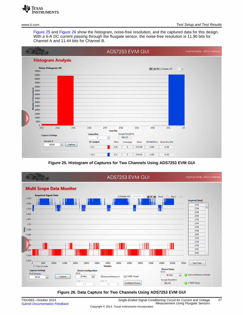
Figure 25 and Figure 26 show the histogram, noise-free resolution, and the captured data for this design.With a 6-A DC current passing through the fluxgate sensor, the noise-free resolution is 11.90 bits forChannel A and 11.44 bits for Channel B.
Figure 25. Histogram of Captures for Two Channels Using ADS7253 EVM GUI
Figure 26. Data Capture for Two Channels Using ADS7253 EVM GUI
27TIDU583–October 2014 Single-Ended Signal Conditioning Circuit for Current and VoltageMeasurement Using Fluxgate SensorsSubmit Documentation Feedback
9.3 AC (or Static) Performance of the System Using External ADC ADS7253For any data acquisition system, an important focus is to achieve excellent dynamic performance whileminimizing the total power consumption of the system. The main AC specifications to consider are THD,SNR, SINAD, and ENOB. Essentially, these parameters are different ways of quantifying the noise anddistortion performance of an ADC based on a fast Fourier transform (FFT) analysis. A typical FFT plot foran ADC is shown in Figure 27.
Figure 27. Typical FFT Plot Showing Different Dynamic Parameters
The SNR provides insight into the total noise of the system. The total noise of the data acquisition systemis the RSS of the front-end amplifier noise (Vn_AMP_RMS) and the ADC noise (Vn_ADC_RMS). The ADC noiseincludes the quantization noise as well as the noise contributed by the ADC internal circuitry, or the input-referred noise of the ADC. The total noise contributions from all these sources, denoted as Vn_TOT_RMS, arereferred to the input of the ADC to calculate the total SNR of the system (SNRSYS).
(5)
ENOB is an effective measurement of the quality of a digitized signal from an ADC by specifying thenumber of bits above the noise floor. For an ideal N-bit ADC with only quantization noise, the SNR (in dB)can be calculated as:
(6)
While ENOB provides a good summary of the ADC dynamic performance, it does not describe theconverter's entire performance over the operating frequency ranges and input signals. Additionally, ENOBdoes not include the ADC DC specifications such as offset and gain error. Therefore, pay attention toother converter specifications as well depending on the application using the ADC.
28 Single-Ended Signal Conditioning Circuit for Current and Voltage TIDU583–October 2014Measurement Using Fluxgate Sensors Submit Documentation Feedback
For an AC current of 4.5 VRMS at a frequency of 50 Hz, the conditioned voltage signal (at the output ofADS7253) is captured, and the FFT of the system is also taken using the ADS7253EVM and SDCCboard. As shown in Figure 28 and Figure 29, the GUI captures show the captured AC signal, the FFT, andother parameters.
Figure 28. AC Signal Capture for Two Channels Using ADS7253 EVM GUI
Figure 29. FFT and SNR Shown for Two Channels Using ADS7253 EVM GUI
29TIDU583–October 2014 Single-Ended Signal Conditioning Circuit for Current and VoltageMeasurement Using Fluxgate SensorsSubmit Documentation Feedback
The FFT for both channels show an SNR of approximately 67.5 dB at a signal amplitude of –8.9 dBFS.This result is just an indication of performance, but the actual SNR can be measured when the device isoperated with an input voltage that has reached the full-scale value of the ADC input range. Figure 30 isthe setup used to measure the AC and DC performance for this reference design.
Figure 30. Test Setup for AC and DC Tests for ADS7253
30 Single-Ended Signal Conditioning Circuit for Current and Voltage TIDU583–October 2014Measurement Using Fluxgate Sensors Submit Documentation Feedback
9.4 DC Accuracy Tests (at 25°C and 75°C)The following figures show the accuracy of the signal at each stage. Figure 31 shows accuracy of signal atthe output of THS4531 at 25°C and Figure 32 shows accuracy of signal at 75°C. It includes the offset andgain error compensation along with passive component mismatches in the feedback path of THS4531.
Figure 31. Op-Amp Accuracy at 25°C (Left) for Positive Current (Right) for Negative Current
Figure 32. Op-Amp Accuracy at 75°C (Left) for Positive Current (Right) for Negative Current
31TIDU583–October 2014 Single-Ended Signal Conditioning Circuit for Current and VoltageMeasurement Using Fluxgate SensorsSubmit Documentation Feedback
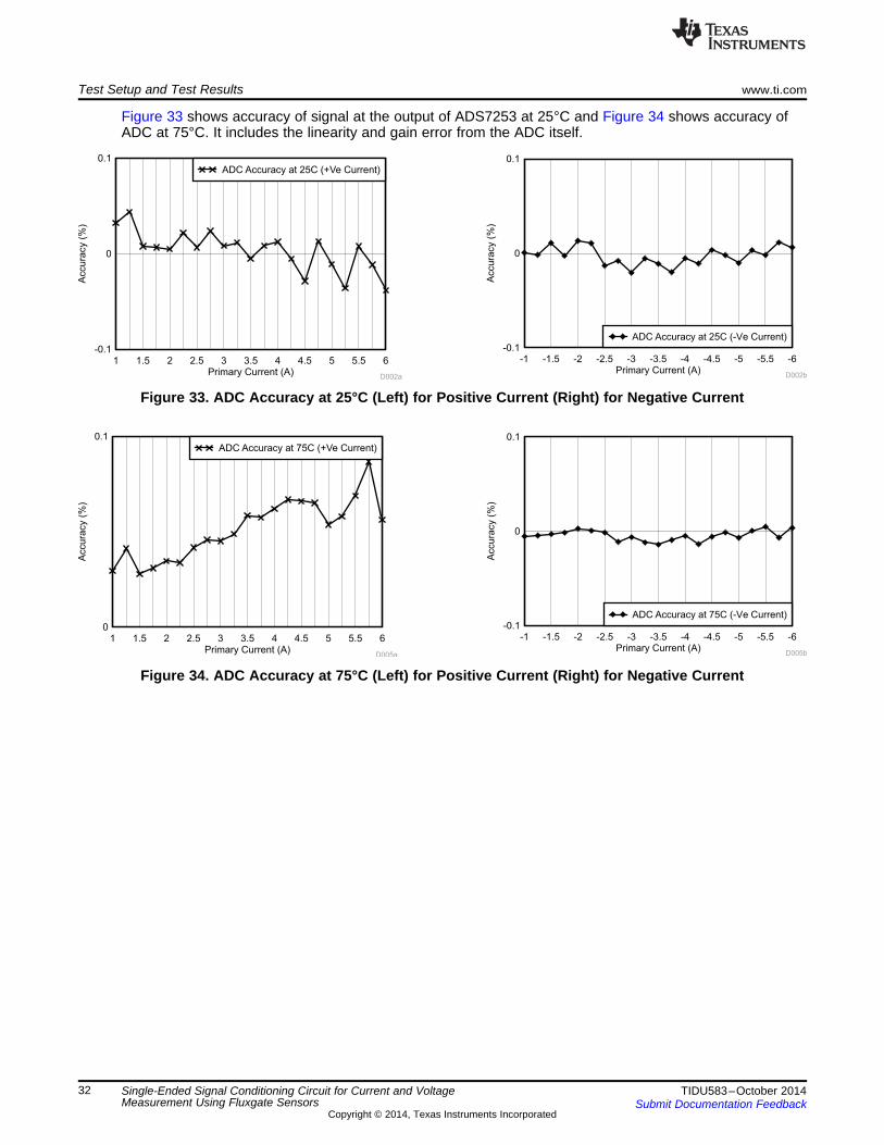
Figure 33 shows accuracy of signal at the output of ADS7253 at 25°C and Figure 34 shows accuracy ofADC at 75°C. It includes the linearity and gain error from the ADC itself.
Figure 33. ADC Accuracy at 25°C (Left) for Positive Current (Right) for Negative Current
Figure 34. ADC Accuracy at 75°C (Left) for Positive Current (Right) for Negative Current
32 Single-Ended Signal Conditioning Circuit for Current and Voltage TIDU583–October 2014Measurement Using Fluxgate Sensors Submit Documentation Feedback
Figure 35 shows accuracy of signal for the entire signal chain (FDA + ADC) at 25°C and Figure 36 showsthe total accuracy at 75°C. Note that in a typical drive application, the current sensor would be used from30% to 100% of its nominal current rating so the accuracy should be considered for primary current from±1.75A to ±6A.
Figure 35. Total Accuracy at 25°C (Left) for Positive Current (Right) for Negative Current
Figure 36. Total Accuracy at 75°C (Left) for Positive Current (Right) for Negative Current
33TIDU583–October 2014 Single-Ended Signal Conditioning Circuit for Current and VoltageMeasurement Using Fluxgate SensorsSubmit Documentation Feedback
9.5 DC Accuracy Tests Using Piccolo 28027 Internal ADC (on LaunchPad)The accuracy of Internal ADC of Piccolo 28027 controller is measured along with the fluxgate-basedreference design. Figure 37 shows the screenshot capture of ADC output code GUI. The total accuracycurve is as shown in Figure 38.
Figure 37. Screenshot of Internal ADC GUI for Piccolo Controller
Figure 38. Total Accuracy While Using Internal ADC of Piccolo 28027 Controller(Left) for Positive Current (Right) for Negative Current
34 Single-Ended Signal Conditioning Circuit for Current and Voltage TIDU583–October 2014Measurement Using Fluxgate Sensors Submit Documentation Feedback
9.5.1 AC (or Dynamic) Performance Using Piccolo 28027 Internal ADCFor an AC current of 4.5 VRMS at a frequency of 50 Hz, the conditioned voltage signal (at the output ofOPA4322) is captured, and the FFT of the system is also taken using the Piccolo 28027 LaunchPad.Figure 39 shows the captured signal. Note the time period X2-X1 (= 20.05457026 ms), which correspondsto the 49.86-Hz frequency.
Figure 39. Signal Capture Using Piccolo 28027 LaunchPad
35TIDU583–October 2014 Single-Ended Signal Conditioning Circuit for Current and VoltageMeasurement Using Fluxgate SensorsSubmit Documentation Feedback
9.6 Power Supply and Reference Circuit Functionality TestsThe power supply circuit is tested for functionality and ripple measurement. Figure 40 shows the output ofTPS7A4700 set at 5 V.
Figure 40. 5-V Signal From TPS7A4700
Figure 41 shows the 3.3-V digital supply voltage generated using TLV70033.
Figure 41. 3.3-V Reference Signal Generated by TLV70033
36 Single-Ended Signal Conditioning Circuit for Current and Voltage TIDU583–October 2014Measurement Using Fluxgate Sensors Submit Documentation Feedback
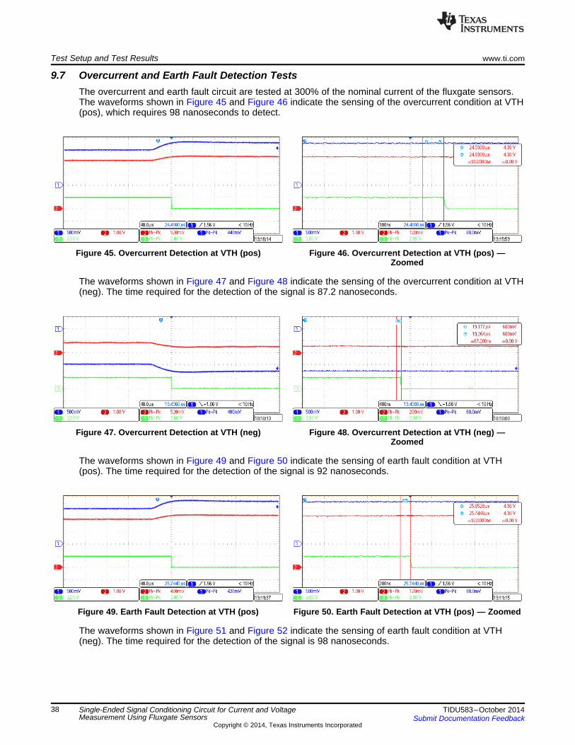
9.7 Overcurrent and Earth Fault Detection TestsThe overcurrent and earth fault circuit are tested at 300% of the nominal current of the fluxgate sensors.The waveforms shown in Figure 45 and Figure 46 indicate the sensing of the overcurrent condition at VTH(pos), which requires 98 nanoseconds to detect.
Figure 45. Overcurrent Detection at VTH (pos) Figure 46. Overcurrent Detection at VTH (pos) —Zoomed
The waveforms shown in Figure 47 and Figure 48 indicate the sensing of the overcurrent condition at VTH(neg). The time required for the detection of the signal is 87.2 nanoseconds.
Figure 47. Overcurrent Detection at VTH (neg) Figure 48. Overcurrent Detection at VTH (neg) —Zoomed
The waveforms shown in Figure 49 and Figure 50 indicate the sensing of earth fault condition at VTH(pos). The time required for the detection of the signal is 92 nanoseconds.
Figure 49. Earth Fault Detection at VTH (pos) Figure 50. Earth Fault Detection at VTH (pos) — Zoomed
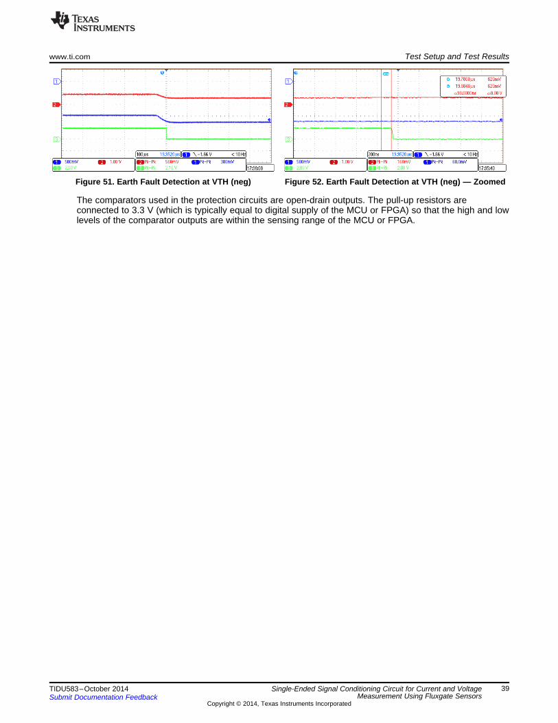
The waveforms shown in Figure 51 and Figure 52 indicate the sensing of earth fault condition at VTH(neg). The time required for the detection of the signal is 98 nanoseconds.
38 Single-Ended Signal Conditioning Circuit for Current and Voltage TIDU583–October 2014Measurement Using Fluxgate Sensors Submit Documentation Feedback
Figure 51. Earth Fault Detection at VTH (neg) Figure 52. Earth Fault Detection at VTH (neg) — Zoomed
The comparators used in the protection circuits are open-drain outputs. The pull-up resistors areconnected to 3.3 V (which is typically equal to digital supply of the MCU or FPGA) so that the high and lowlevels of the comparator outputs are within the sensing range of the MCU or FPGA.
39TIDU583–October 2014 Single-Ended Signal Conditioning Circuit for Current and VoltageMeasurement Using Fluxgate SensorsSubmit Documentation Feedback
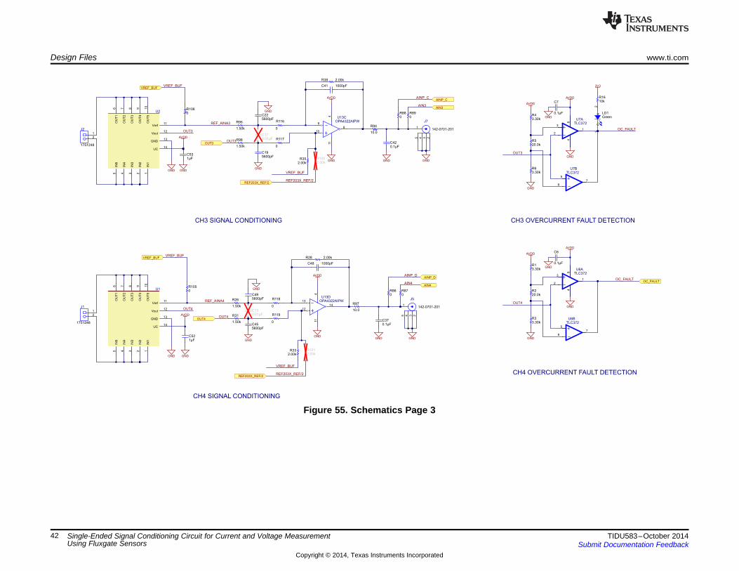
10.1 SchematicsTo download the schematics, see the design files at TIDA-00208.
Figure 53. Schematics Page 1
40 Single-Ended Signal Conditioning Circuit for Current and Voltage Measurement TIDU583–October 2014Using Fluxgate Sensors Submit Documentation Feedback
42 Single-Ended Signal Conditioning Circuit for Current and Voltage Measurement TIDU583–October 2014Using Fluxgate Sensors Submit Documentation Feedback
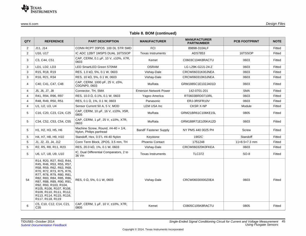
10.2 Bill of MaterialsTo download the bill of materials (BOM), see the design files at TIDA-00208.
Table 8. BOM
MANUFACTURERQTY REFERENCE PART DESCRIPTION MANUFACTURER PCB FOOTPRINT NOTEPARTNUMBER1 !PCB Printed Circuit Board Any TIDA-00208 Fitted
CAP, CERM, 10 µF, 16 V, ±20%, X5R,1 C4 Taiyo Yuden EMK107BBJ106MA-T 0603 Fitted06031 D1 Diode, Schottky, 60 V, 1 A, SMA ON Semiconductor MBRA160T3G SMA Fitted1 J10 Receptacle, 100 mil, 3×1, TH TE Connectivity 534237-1 Receptacle, 100 mil, 3×1 Fitted1 J13 Connector, DC Jack 2.1×5.5 mm, TH CUI Inc. PJ-102A Power Jack, 14.4×11×9 mm Fitted1 J15 Header, Male 8-pin, 100-mil spacing Sullins PEC08SAAN 0.100 inch × 8 Fitted
Terminal Block, 2×1, 2.54 mm,1 J9 Terminal Block, 2×1, 2.54 mm, TH TE Connectivity 282834-2 FittedTHThermal Transfer Printable Labels, PCB Label 0.650" H × 0.200"1 LBL1 Brady THT-14-423-10 Fitted0.650" W × 0.200" H - 10,000 per roll W
44 Single-Ended Signal Conditioning Circuit for Current and Voltage Measurement TIDU583–October 2014Using Fluxgate Sensors Submit Documentation Feedback
46 Single-Ended Signal Conditioning Circuit for Current and Voltage Measurement TIDU583–October 2014Using Fluxgate Sensors Submit Documentation Feedback
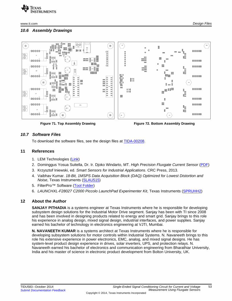
10.3 PCB LayoutTo download the layer plots, see the design files at TIDA-00208.
NOTE: The total dimension of the board is 120 × 100 mm.
10.3.1 Layout Guidelines
Layout of Amplifier SectionThe OPA4322 is a wideband amplifier. To realize the full operational performance of the device:1. Follow good high-frequency PCB layout practices.2. Connect the bypass capacitors between each supply pin and ground as close to the device as
possible.3. Design the bypass capacitor traces for minimum inductance.
Layout of ADC SectionThe most important considerations in designing the PCB layout are as follows:1. Keep the length of traces from the reference buffer circuit (REF and OPA) to the REFP input pin of the
ADC as small as possible to minimize the trace inductance that can lead to instability and potentialissues with the accurate settling of the reference voltage.
2. Locate the input driver circuit as close as possible to the inputs of the ADC to minimize loop area,making the layout more robust against EMI/RFI rejection. Similarly, keep the resistors and capacitor ofthe anti-aliasing filter at the inputs of the ADC close together and close to the inputs of the ADC tominimize the loop area.
3. Use a ground plane underneath the device and partition the PCB into analog and digital sections.Avoid crossing digital lines with the analog signal path and keep the analog input signals and thereference input signals away from noise sources.
4. Keep the power sources to the device clean and well-bypassed. Use 10-μF, ceramic bypass capacitorsin close proximity to the analog (AVDD) and digital (DVDD) power-supply pins. Avoid placing viasbetween the AVDD and DVDD pins and the bypass capacitors. Connect all ground pins to the groundplane using short, low impedance paths.
5. Bypass the REFIO-A and REFIO-B reference inputs and outputs with 10-μF, X7R-grade, 0805-size,16-V rated ceramic capacitors (CREF-x). Place the reference bypass capacitors as close as possibleto the reference REFIO-x pins and connect the bypass capacitors using short, low-inductanceconnections. Avoid placing vias between the REFIO-x pins and the bypass capacitors. Use small 0.1-Ωto 0.2-Ω resistors (RREF-x) in series with the reference bypass capacitors to improve stability.
6. Place the fly-wheel RC filters immediately next to the input pins. Among ceramic surface-mountcapacitors, COG (NPO) ceramic capacitors provide the best capacitance precision. The type ofdielectric used in COG (NPO) ceramic capacitors provides the most stable electrical properties overvoltage, frequency, and temperature changes.
47TIDU583–October 2014 Single-Ended Signal Conditioning Circuit for Current and VoltageMeasurement Using Fluxgate SensorsSubmit Documentation Feedback
48 Single-Ended Signal Conditioning Circuit for Current and Voltage TIDU583–October 2014Measurement Using Fluxgate Sensors Submit Documentation Feedback
50 Single-Ended Signal Conditioning Circuit for Current and Voltage TIDU583–October 2014Measurement Using Fluxgate Sensors Submit Documentation Feedback
10.5 Gerber FilesTo download the Gerber files, see the design files at TIDA-00208.
Figure 70. Fabrication Drawing
52 Single-Ended Signal Conditioning Circuit for Current and Voltage Measurement TIDU583–October 2014Using Fluxgate Sensors Submit Documentation Feedback
12 About the AuthorSANJAY PITHADIA is a systems engineer at Texas Instruments where he is responsible for developingsubsystem design solutions for the Industrial Motor Drive segment. Sanjay has been with TI since 2008and has been involved in designing products related to energy and smart grid. Sanjay brings to this rolehis experience in analog design, mixed signal design, industrial interfaces, and power supplies. Sanjayearned his bachelor of technology in electronics engineering at VJTI, Mumbai.
N. NAVANEETH KUMAR is a systems architect at Texas Instruments where he is responsible fordeveloping subsystem solutions for motor controls within Industrial Systems. N. Navaneeth brings to thisrole his extensive experience in power electronics, EMC, analog, and mixed signal designs. He hassystem-level product design experience in drives, solar inverters, UPS, and protection relays. N.Navaneeth earned his bachelor of electronics and communication engineering from Bharathiar University,India and his master of science in electronic product development from Bolton University, UK.
53TIDU583–October 2014 Single-Ended Signal Conditioning Circuit for Current and VoltageMeasurement Using Fluxgate SensorsSubmit Documentation Feedback
Texas Instruments Incorporated ("TI") reference designs are solely intended to assist designers (“Buyers”) who are developing systems thatincorporate TI semiconductor products (also referred to herein as “components”). Buyer understands and agrees that Buyer remainsresponsible for using its independent analysis, evaluation and judgment in designing Buyer’s systems and products.TI reference designs have been created using standard laboratory conditions and engineering practices. TI has not conducted anytesting other than that specifically described in the published documentation for a particular reference design. TI may makecorrections, enhancements, improvements and other changes to its reference designs.Buyers are authorized to use TI reference designs with the TI component(s) identified in each particular reference design and to modify thereference design in the development of their end products. HOWEVER, NO OTHER LICENSE, EXPRESS OR IMPLIED, BY ESTOPPELOR OTHERWISE TO ANY OTHER TI INTELLECTUAL PROPERTY RIGHT, AND NO LICENSE TO ANY THIRD PARTY TECHNOLOGYOR INTELLECTUAL PROPERTY RIGHT, IS GRANTED HEREIN, including but not limited to any patent right, copyright, mask work right,or other intellectual property right relating to any combination, machine, or process in which TI components or services are used.Information published by TI regarding third-party products or services does not constitute a license to use such products or services, or awarranty or endorsement thereof. Use of such information may require a license from a third party under the patents or other intellectualproperty of the third party, or a license from TI under the patents or other intellectual property of TI.TI REFERENCE DESIGNS ARE PROVIDED "AS IS". TI MAKES NO WARRANTIES OR REPRESENTATIONS WITH REGARD TO THEREFERENCE DESIGNS OR USE OF THE REFERENCE DESIGNS, EXPRESS, IMPLIED OR STATUTORY, INCLUDING ACCURACY ORCOMPLETENESS. TI DISCLAIMS ANY WARRANTY OF TITLE AND ANY IMPLIED WARRANTIES OF MERCHANTABILITY, FITNESSFOR A PARTICULAR PURPOSE, QUIET ENJOYMENT, QUIET POSSESSION, AND NON-INFRINGEMENT OF ANY THIRD PARTYINTELLECTUAL PROPERTY RIGHTS WITH REGARD TO TI REFERENCE DESIGNS OR USE THEREOF. TI SHALL NOT BE LIABLEFOR AND SHALL NOT DEFEND OR INDEMNIFY BUYERS AGAINST ANY THIRD PARTY INFRINGEMENT CLAIM THAT RELATES TOOR IS BASED ON A COMBINATION OF COMPONENTS PROVIDED IN A TI REFERENCE DESIGN. IN NO EVENT SHALL TI BELIABLE FOR ANY ACTUAL, SPECIAL, INCIDENTAL, CONSEQUENTIAL OR INDIRECT DAMAGES, HOWEVER CAUSED, ON ANYTHEORY OF LIABILITY AND WHETHER OR NOT TI HAS BEEN ADVISED OF THE POSSIBILITY OF SUCH DAMAGES, ARISING INANY WAY OUT OF TI REFERENCE DESIGNS OR BUYER’S USE OF TI REFERENCE DESIGNS.TI reserves the right to make corrections, enhancements, improvements and other changes to its semiconductor products and services perJESD46, latest issue, and to discontinue any product or service per JESD48, latest issue. Buyers should obtain the latest relevantinformation before placing orders and should verify that such information is current and complete. All semiconductor products are soldsubject to TI’s terms and conditions of sale supplied at the time of order acknowledgment.TI warrants performance of its components to the specifications applicable at the time of sale, in accordance with the warranty in TI’s termsand conditions of sale of semiconductor products. Testing and other quality control techniques for TI components are used to the extent TIdeems necessary to support this warranty. Except where mandated by applicable law, testing of all parameters of each component is notnecessarily performed.TI assumes no liability for applications assistance or the design of Buyers’ products. Buyers are responsible for their products andapplications using TI components. To minimize the risks associated with Buyers’ products and applications, Buyers should provideadequate design and operating safeguards.Reproduction of significant portions of TI information in TI data books, data sheets or reference designs is permissible only if reproduction iswithout alteration and is accompanied by all associated warranties, conditions, limitations, and notices. TI is not responsible or liable forsuch altered documentation. Information of third parties may be subject to additional restrictions.Buyer acknowledges and agrees that it is solely responsible for compliance with all legal, regulatory and safety-related requirementsconcerning its products, and any use of TI components in its applications, notwithstanding any applications-related information or supportthat may be provided by TI. Buyer represents and agrees that it has all the necessary expertise to create and implement safeguards thatanticipate dangerous failures, monitor failures and their consequences, lessen the likelihood of dangerous failures and take appropriateremedial actions. Buyer will fully indemnify TI and its representatives against any damages arising out of the use of any TI components inBuyer’s safety-critical applications.In some cases, TI components may be promoted specifically to facilitate safety-related applications. With such components, TI’s goal is tohelp enable customers to design and create their own end-product solutions that meet applicable functional safety standards andrequirements. Nonetheless, such components are subject to these terms.No TI components are authorized for use in FDA Class III (or similar life-critical medical equipment) unless authorized officers of the partieshave executed an agreement specifically governing such use.Only those TI components that TI has specifically designated as military grade or “enhanced plastic” are designed and intended for use inmilitary/aerospace applications or environments. Buyer acknowledges and agrees that any military or aerospace use of TI components thathave not been so designated is solely at Buyer's risk, and Buyer is solely responsible for compliance with all legal and regulatoryrequirements in connection with such use.TI has specifically designated certain components as meeting ISO/TS16949 requirements, mainly for automotive use. In any case of use ofnon-designated products, TI will not be responsible for any failure to meet ISO/TS16949.IMPORTANT NOTICE