SANKEN ELECTRIC CO., LTD. http://www.sanken-ele.co.jp/en/ SLA7070MPRT Series Unipolar 2-Phase Stepper Motor Driver ICs Application Information SLA7070MPRT-AN, Rev. 1.4 General Description This document describes the SLA7070MPRT series, which are unipolar 2-phase stepping motor driver ICs. The SLA7070MPRT series employs a clock input method as a control signal input method, enabling full control of the device operation using only a few signal lines, instead of the conventional phase input method that requires about 10 signal lines. This allows simplification of the circuit design and a reduced workload on the control microprocessor. In addition, the SLA7070MPRT series is improved in its reliability by preventing the IC from damage due to abnor- mal conditions. For example, it has a flag output terminal to signal that a protection circuit has operated. The series also has a built-in protection circuitry against motor coil opens/shorts and thermal shutdown protection as well. All the SLA7070MPRT series ICs are compatible in their pin layouts and interface specifications, allowing custom- ers the flexibility of choosing the IC that is optimal for the target equipment characteristics. Features and Benefits • Power supply voltages, V BB : 46 V (max.), 10 to 44 V normal operating range • Logic supply voltages, V DD : 3.0 to 5.5 V • Maximum output currents: 1 A, 1.5 A, 2 A, 3 A • Built-in sequencer • Full-, half-, and microstepping available (microstepping options are capable of full-, half-, quarter-, eighth-, and sixteenth-stepping Figure 1. SLA7070MPRT packages are fully molded ZIPs with an exposed pad for heatsink mounting. The SLA7070MMPR series product variants and optional features Part Number Stepping Rate Output Current (I OUT ) (A) Input Clock Edge Detection Blanking Time (μs) Standard Standard SLA7070MPRT Full and half step 1 Rising (positive) edge 3.2 SLA7071MPRT 1.5 SLA7072MPRT 2 SLA7073MPRT 3 SLA7075MPRT Microstep 1 Rising (positive) edge 1.7 SLA7076MPRT 1.5 SLA7077MPRT 2 SLA7078MPRT 3 • Built-in sense resistor, R SInt • All variants are pin-compatible for enhanced design flexibility • ZIP type 23-pin molded package (SLA package) • Self-excitation PWM current control with fixed off-time (microstepping options off-time adjusted automatically by step reference current ratio; 3 levels) • Built-in synchronous rectifying circuit reduces losses at PWM-off • Synchronous PWM chopping function prevents motor noise in Hold mode • Sleep mode for reducing the IC input current in stand-by state • Built-in protection circuitry against motor coil opens/shorts and thermal shutdown protection options Applications • LBPs, PPCs, ATMs, industrial robots, and so forth January 10, 2013
Transcript
SANKEN ELECTRIC CO., LTD.http://www.sanken-ele.co.jp/en/
SLA7070MPRT Series Unipolar 2-Phase Stepper Motor Driver ICs
Application Information
SLA7070MPRT-AN, Rev. 1.4
General DescriptionThis document describes the SLA7070MPRT series, which are unipolar 2-phase stepping motor driver ICs. The SLA7070MPRT series employs a clock input method as a control signal input method, enabling full control of the device operation using only a few signal lines, instead of the conventional phase input method that requires about 10 signal lines. This allows simplification of the circuit design and a reduced workload on the control microprocessor.
In addition, the SLA7070MPRT series is improved in its reliability by preventing the IC from damage due to abnor-mal conditions. For example, it has a flag output terminal to signal that a protection circuit has operated. The series also has a built-in protection circuitry against motor coil opens/shorts and thermal shutdown protection as well.
All the SLA7070MPRT series ICs are compatible in their pin layouts and interface specifications, allowing custom-ers the flexibility of choosing the IC that is optimal for the target equipment characteristics.
Features and Benefits• Power supply voltages, VBB : 46 V (max.), 10 to 44 V
normal operating range• Logic supply voltages, VDD : 3.0 to 5.5 V• Maximum output currents: 1 A, 1.5 A, 2 A, 3 A• Built-in sequencer• Full-, half-, and microstepping available (microstepping
options are capable of full-, half-, quarter-, eighth-, and sixteenth-stepping
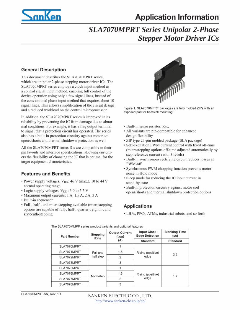
Figure 1. SLA7070MPRT packages are fully molded ZIPs with an exposed pad for heatsink mounting.
The SLA7070MMPR series product variants and optional features
Part Number SteppingRate
Output Current(IOUT)(A)
Input Clock Edge Detection
Blanking Time(μs)
Standard StandardSLA7070MPRT
Full and half step
1
Rising (positive) edge 3.2
SLA7071MPRT 1.5
SLA7072MPRT 2
SLA7073MPRT 3
SLA7075MPRT
Microstep
1
Rising (positive) edge 1.7
SLA7076MPRT 1.5
SLA7077MPRT 2
SLA7078MPRT 3
• Built-in sense resistor, RSInt• All variants are pin-compatible for enhanced
design flexibility• ZIP type 23-pin molded package (SLA package)• Self-excitation PWM current control with fixed off-time
(microstepping options off-time adjusted automatically by step reference current ratio; 3 levels)
• Built-in synchronous rectifying circuit reduces losses at PWM-off
• Synchronous PWM chopping function prevents motor noise in Hold mode
• Sleep mode for reducing the IC input current in stand-by state
• Built-in protection circuitry against motor coil opens/shorts and thermal shutdown protection options
Applications• LBPs, PPCs, ATMs, industrial robots, and so forth
Monolithic IC (MIC) 22Output MOSFET Chip 22Sense Resistor 22
Functional Description 23PWM Current Control 23
Blanking Time 23PWM Off-Time 26Protection Functions 27
Application Information 29Motor Current Ratio Setting (R1, R2, RS) 29Lower Limit of Control Current 29Avalanche Energy 29On-Off Sequence of Power Supply (VBB and VDD) 30Motor Supply Voltage (VM) and Main Power Supply Voltage (VBB) 31Internal Logic Circuits 31
Thermal Design Information 32Characteristic Data 34
3SANKEN ELECTRIC CO., LTD.
SLA7070MPRT-AN, Rev. 1.4
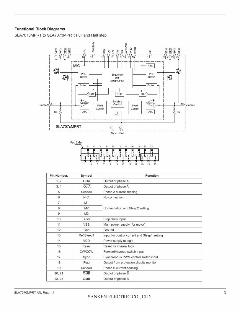
Functional Block DiagramsSLA7070MPRT to SLA7073MPRT: Full and Half step
Sequencerand
Sleep Circuit
SynchroControlPWM
ControlOSC
Comp+-
DAC
Pre-Driver
PWMControl
OSC
DAC
Pre-Driver
+-
MIC
SLA707xMPRT
Reg.
OutA
OutA
OutA
OutA
OutB
OutB
OutB
OutB
VD
D
Ref/Sleep1
Flag
N.C.
M1
M2
M3
CW/C
CW
Clock
Reset
VBB
SenseBSenseA
GndSync
Rs Rs
1 2 3 4
5
6 7 8 9 10 11
12
1314 1516
17
18
19
20 21 22 23
Protect Protect
TSD
Comp
Pin Number. Symbol Function1, 2 OutA Output of phase A
3, 4 O u t A Output of phase A
5 SenseA Phase A current sensing
6 N.C. No connection
7 M1
Commutation and Sleep2 setting8 M2
9 M3
10 Clock Step clock input
11 VBB Main power supply (for motor)
12 Gnd Ground
13 Ref/Sleep1 Input for control current and Sleep1 setting
14 VDD Power supply to logic
15 Reset Reset for internal logic
16 CW/CCW Forward/reverse switch input
17 Sync Synchronous PWM control switch input
18 Flag Output from protection circuits monitor
19 SenseB Phase B current sensing
20, 21 O u t B Output of phase B
22, 23 OutB Output of phase B
1 3 5 7 9 11 13 15 17 19 21 23
2 4 6 8 10 12 14 16 18 20 22Pad Side
4SANKEN ELECTRIC CO., LTD.
SLA7070MPRT-AN, Rev. 1.4
Sequencerand
Sleep Circuit
SynchroControlPWM
ControlOSC
+-
DAC
Pre-Driver
PWMControl
OSC
DAC
Pre-Driver
+-
Reg.
OutA
OutA
OutA
OutA
OutB
OutB
OutB
OutB
VD
D
Ref/Sleep1
Flag
MO
M1
M2
M3
Clock
Reset
VBB
SenseBSenseA
GndSync
Rs Rs
1 2 3 4
5
6 7 8 9 10 11
12
1314 1516
17
18
19
20 21 22 23
Protect Protect
TSD
CW/C
CW
Comp Comp
MIC
SLA707xMPRT
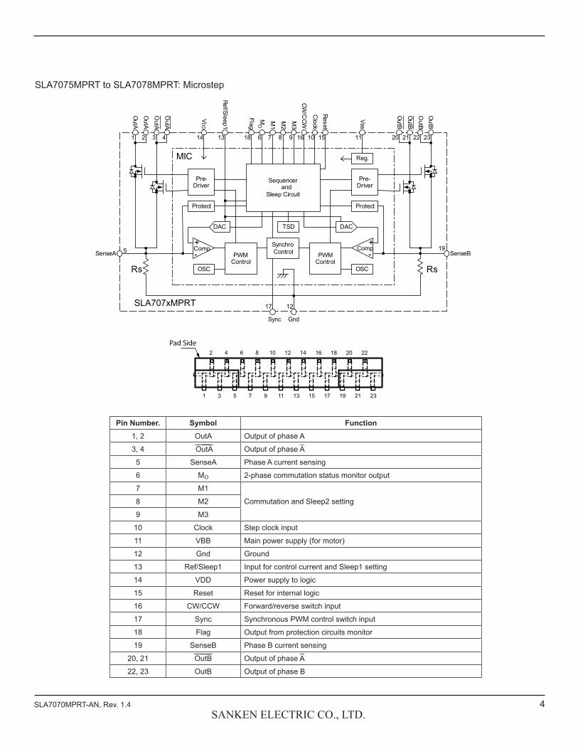
SLA7075MPRT to SLA7078MPRT: Microstep
Pin Number. Symbol Function1, 2 OutA Output of phase A
3, 4 O u t A Output of phase A
5 SenseA Phase A current sensing
6 MO 2-phase commutation status monitor output
7 M1
Commutation and Sleep2 setting8 M2
9 M3
10 Clock Step clock input
11 VBB Main power supply (for motor)
12 Gnd Ground
13 Ref/Sleep1 Input for control current and Sleep1 setting
14 VDD Power supply to logic
15 Reset Reset for internal logic
16 CW/CCW Forward/reverse switch input
17 Sync Synchronous PWM control switch input
18 Flag Output from protection circuits monitor
19 SenseB Phase B current sensing
20, 21 O u t B Output of phase A
22, 23 OutB Output of phase B
1 3 5 7 9 11 13 15 17 19 21 23
2 4 6 8 10 12 14 16 18 20 22Pad Side
5SANKEN ELECTRIC CO., LTD.
SLA7070MPRT-AN, Rev. 1.4
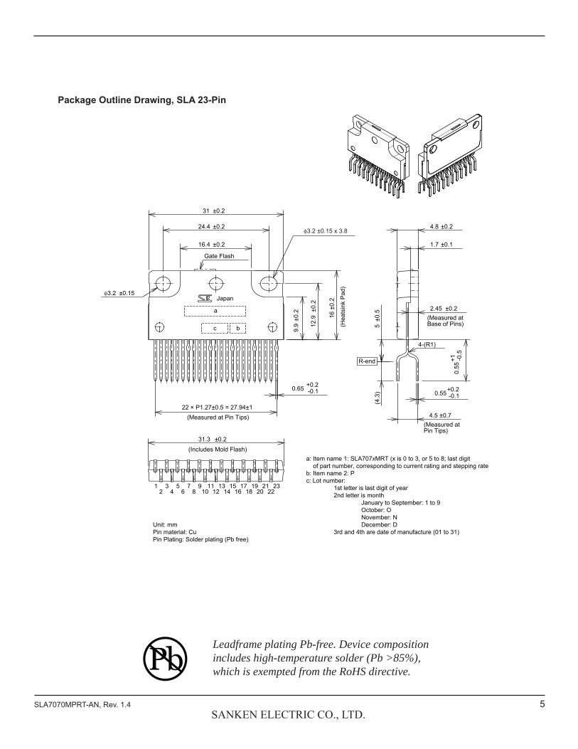
Leadframe plating Pb-free. Device composition includes high-temperature solder (Pb >85%), which is exempted from the RoHS directive.
1.7 ±0.1
4.8 ±0.2
16.4 ±0.2
31 ±0.2
24.4 ±0.2
3.2 ±0.15
12.9
±0.2
0.65 +0.2-0.1
16±0
.2
9.9
±0.2
4-(R1)
5±0
.5
0.55+0.2-0.1
0.55
+1 -0.5
4.522 × P1.27±0.5 = 27.94±1
±0.7
R-end
31.3 ±0.2
12
34 10
1156
78
912
1314
1516
1718
1920
2122
23
(Includes Mold Flash)
2.45 ±0.2(Measured atBase of Pins)
(Measured at Pin Tips)
Unit: mmPin material: CuPin Plating: Solder plating (Pb free)
a: Item name 1: SLA707xMRT (x is 0 to 3, or 5 to 8; last digit of part number, corresponding to current rating and stepping rate)b: Item name 2: Pc: Lot number: 1st letter is last digit of year 2nd letter is month January to September: 1 to 9 October: O November: N December: D 3rd and 4th are date of manufacture (01 to 31)
(Measured at Pin Tips)
(Hea
tsin
k P
ad)
Gate Flash
Japan
a
bc
(4.3
)
3.2 ±0.15 x 3.8
Package Outline Drawing, SLA 23-Pin
6SANKEN ELECTRIC CO., LTD.
SLA7070MPRT-AN, Rev. 1.4
Recommended Operating Conditions Unless specifically noted, TA is 25°CCharacteristic Symbol Test Conditions Min. Typ. Max. Unit
Load (Motor Supply) Voltage VM – – 44 V
Main Power Supply Voltage VBB 10 – 44 V
Logic Supply Voltage VDD
Surge voltage at VDD pin should be less than ±0.5 V to avoid malfunctioning in operation
3.0 – 5.5 V
Case Temperature TcMeasured at pin 12, without heatsink – – 90 °C
Electrical Characteristics• This section provides separate sets of electrical characteristic data for each product.
• The polarity value for current specifies a sink as "+ ," and a source as “−,” referencing the IC.
• Please refer to the datasheet of each product for additional details.
Absolute Maximum Ratings Unless specifically noted, TA is 25°C Characteristic Symbol Notes Rating Unit
Load (Motor Supply) Voltage VM 46 V
Main Power Supply Voltage VBB 46 V
Logic Supply Voltage VDD6 V
≤1 μs (5% duty) 7 V
Output Current IO
SLA7070MPRTSLA7075MPRT
Control current value
1.0 A
SLA7071MPRTSLA7076MPRT 1.5 A
SLA7072MPRTSLA7077MPRT 2.0 A
SLA7073MPRTSLA7078MPRT 3.0 A
Logic Input Voltage VIN −0.3 to VDD+0.3 V
REF Input Voltage VREF −0.3 to VDD+0.3 V
Sense Voltage VRS ±1 V
Power Dissipation PD Without heatsink 4.7 W
Junction Temperature TJ 150 °C
7SANKEN ELECTRIC CO., LTD.
SLA7070MPRT-AN, Rev. 1.4
Electrical Characteristics Common to All Variants Unless specifically noted, TA is 25°CCharacteristic Symbol Test Conditions Min. Typ. Max. Unit
Main Power Supply CurrentIBB Normal mode – – 15 mA
IBBS Sleep1 and Sleep2 mode – – 100 μA
Logic Power Current IDD – – 5 mA
MOSFET Breakdown Voltage VDSS VBB = 44 V, ID = 1 mA 100 – – V
Maximum Response Frequency fclk Clock duty = 50% 250 – – KHz
Logic Supply VoltageVIL – – 0.25 × VDD V
VIH 0.75 × VDD – – V
Logic Supply CurrentIIL – ±1 – μA
IIH – ±1 – μA
REF Input Voltage1VREF See figure 1 – – – V
VREFS Output off, Sleep1 mode 2.0 – VDD V
REF Input Current IREF – ±10 – μA
SENSE Voltage VSENSEVREF = 0 to 1.5 VStep reference current ratio: 100%
VREF – 0.03 – VREF –
0.03 V
Sleep to Enable Recovery Time tSE Sleep1 and Sleep2 100 – – μs
Switching Timetcon Clock edge to output on – 2.0 – μs
tcoff Clock edge to output off – 1.5 – μs
Overcurrent Detection Voltage2 VOCP At motor coil short-circuit 0.65 0.7 0.75 V
Overcurrent Detection Current ( VOCP / RS )
IOCP
SLA7070MPRT, SLA7075MPRT, SLA7071MPRT, SLA7076MPRT – 2.3 – A
SLA7072MPRT, SLA7077MPRT – 3.5 – A
SLA7073MPRT, SLA7078MPRT – 4.6 – A
Load Disconnection Undetected Time topp From PWM off – 2 – μs
Overheat Protection Temperature TtsdMeasured at back of device case (after heat has saturated) – 140 – °C
Flag Output VoltageVFlagL IFlagL = 1.25 mA – – 1.25 V
VFlagH IFlagH = –1.25 mA VDD – 1.25 – – V
Flag Output CurrentIFlagL – – 1.25 mA
IFlagH –1.25 – – mA1In a state of: Sleep1, IBBS, output off, and Sequencer enabled.2In a condition of VSENSE ≥ VOCP , the protection circuit will activate.
8SANKEN ELECTRIC CO., LTD.
SLA7070MPRT-AN, Rev. 1.4
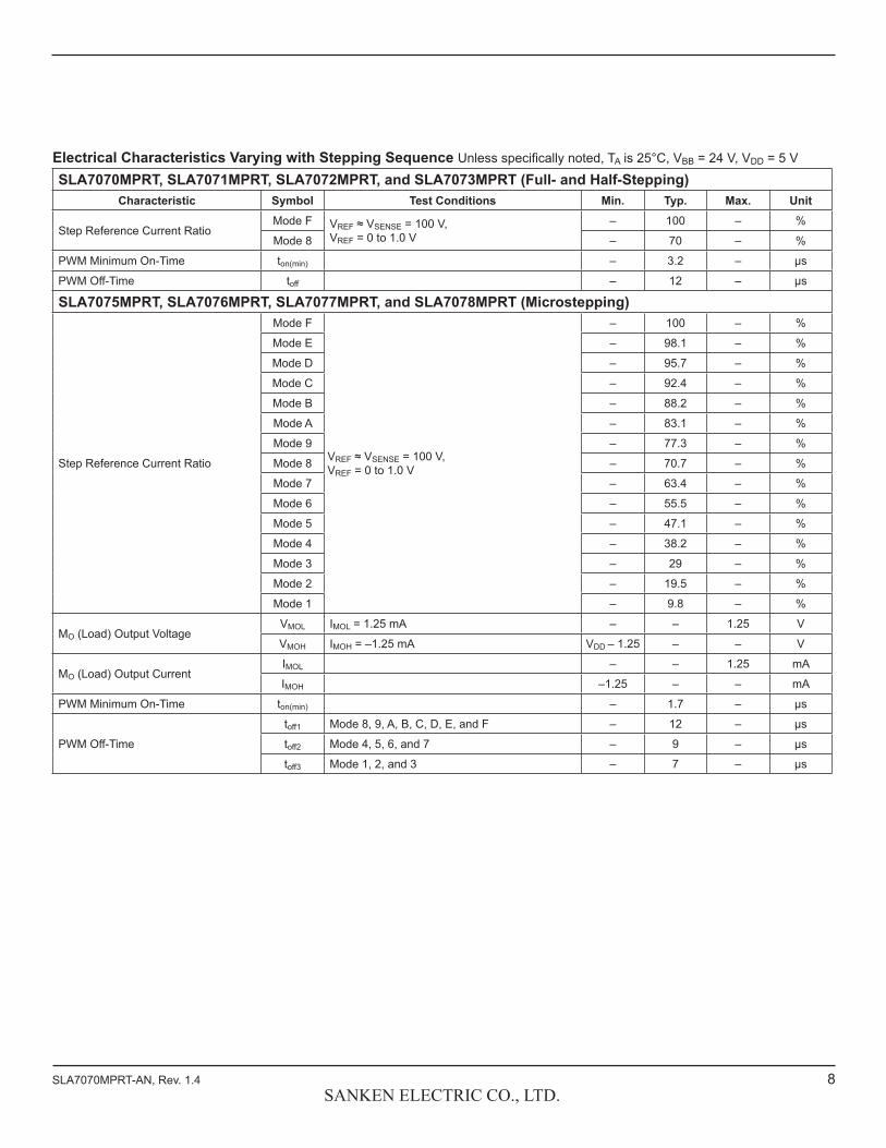
Electrical Characteristics Varying with Stepping Sequence Unless specifically noted, TA is 25°C, VBB = 24 V, VDD = 5 V
SLA7070MPRT, SLA7071MPRT, SLA7072MPRT, and SLA7073MPRT (Full- and Half-Stepping) Characteristic Symbol Test Conditions Min. Typ. Max. Unit
Step Reference Current RatioMode F VREF ≈ VSENSE = 100 V,
VREF = 0 to 1.0 V– 100 – %
Mode 8 – 70 – %
PWM Minimum On-Time ton(min) – 3.2 – μs
PWM Off-Time toff – 12 – μs
SLA7075MPRT, SLA7076MPRT, SLA7077MPRT, and SLA7078MPRT (Microstepping)
Step Reference Current Ratio
Mode F
VREF ≈ VSENSE = 100 V, VREF = 0 to 1.0 V
– 100 – %
Mode E – 98.1 – %
Mode D – 95.7 – %
Mode C – 92.4 – %
Mode B – 88.2 – %
Mode A – 83.1 – %
Mode 9 – 77.3 – %
Mode 8 – 70.7 – %
Mode 7 – 63.4 – %
Mode 6 – 55.5 – %
Mode 5 – 47.1 – %
Mode 4 – 38.2 – %
Mode 3 – 29 – %
Mode 2 – 19.5 – %
Mode 1 – 9.8 – %
MO (Load) Output VoltageVMOL IMOL = 1.25 mA – – 1.25 V
VMOH IMOH = –1.25 mA VDD – 1.25 – – V
MO (Load) Output CurrentIMOL – – 1.25 mA
IMOH –1.25 – – mA
PWM Minimum On-Time ton(min) – 1.7 – μs
PWM Off-Time
toff1 Mode 8, 9, A, B, C, D, E, and F – 12 – μs
toff2 Mode 4, 5, 6, and 7 – 9 – μs
toff3 Mode 1, 2, and 3 – 7 – μs
9SANKEN ELECTRIC CO., LTD.
SLA7070MPRT-AN, Rev. 1.4
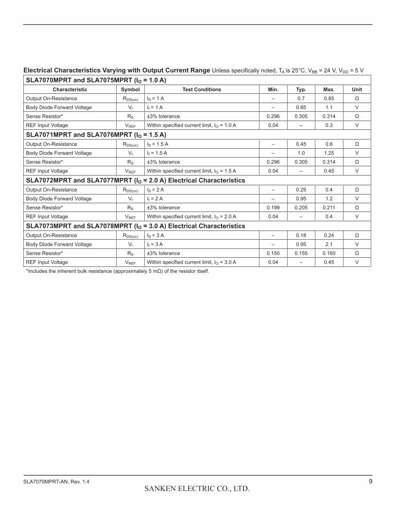
Electrical Characteristics Varying with Output Current Range Unless specifically noted, TA is 25°C, VBB = 24 V, VDD = 5 V
SLA7070MPRT and SLA7075MPRT (IO = 1.0 A) Characteristic Symbol Test Conditions Min. Typ. Max. Unit
Output On-Resistance RDS(on) ID = 1 A – 0.7 0.85 Ω
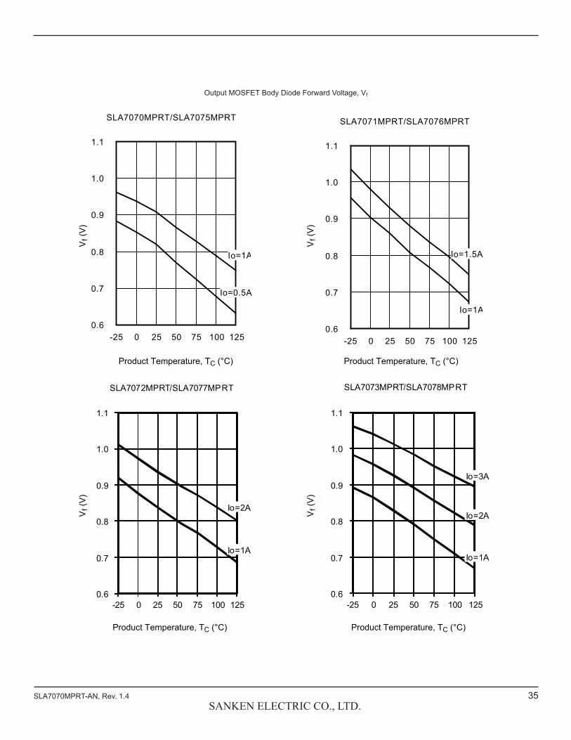
Body Diode Forward Voltage Vf If = 1 A – 0.85 1.1 V
Sense Resistor* RS ±3% tolerance 0.296 0.305 0.314 Ω
REF Input Voltage VREF Within specified current limit, IO = 1.0 A 0.04 – 0.3 V
SLA7071MPRT and SLA7076MPRT (IO = 1.5 A) Output On-Resistance RDS(on) ID = 1.5 A – 0.45 0.6 Ω
Body Diode Forward Voltage Vf If = 1.5 A – 1.0 1.25 V
Sense Resistor* RS ±3% tolerance 0.296 0.305 0.314 Ω
REF Input Voltage VREF Within specified current limit, IO = 1.5 A 0.04 – 0.45 V
SLA7072MPRT and SLA7077MPRT (IO = 2.0 A) Electrical Characteristics Output On-Resistance RDS(on) ID = 2 A – 0.25 0.4 Ω
Body Diode Forward Voltage Vf If = 2 A – 0.95 1.2 V
Sense Resistor* RS ±3% tolerance 0.199 0.205 0.211 Ω
REF Input Voltage VREF Within specified current limit, IO = 2.0 A 0.04 – 0.4 V
SLA7073MPRT and SLA7078MPRT (IO = 3.0 A) Electrical Characteristics Output On-Resistance RDS(on) ID = 3 A – 0.18 0.24 Ω
Body Diode Forward Voltage Vf If = 3 A – 0.95 2.1 V
Sense Resistor* RS ±3% tolerance 0.150 0.155 0.160 Ω
REF Input Voltage VREF Within specified current limit, IO = 3.0 A 0.04 – 0.45 V
*Includes the inherent bulk resistance (approximately 5 mΩ) of the resistor itself.
10SANKEN ELECTRIC CO., LTD.
SLA7070MPRT-AN, Rev. 1.4
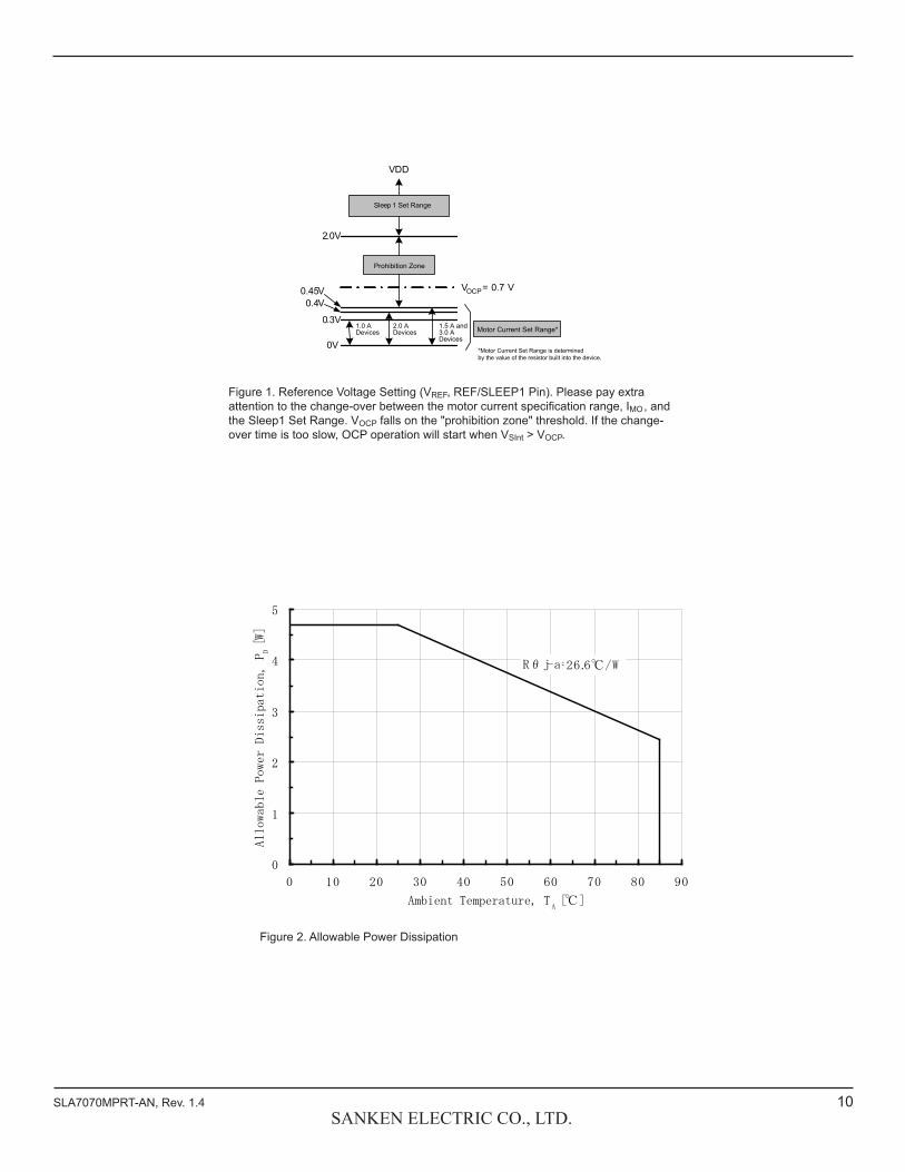
VOCP= 0.7 V
0.3V
VDD
0V
2.0V
Sleep
Prohibition Zone
1 Set Range
0.4V0.45V
1.0 ADevices
2.0 ADevices
1.5 A and3.0 ADevices
Motor Current Set Range*
*Motor Current Set Range is determined by the value of the resistor built into the device.
Figure 1. Reference Voltage Setting (VREF, REF/SLEEP1 Pin). Please pay extra attention to the change-over between the motor current specification range, IMO , and the Sleep1 Set Range. VOCP falls on the "prohibition zone" threshold. If the change-over time is too slow, OCP operation will start when VSInt > VOCP.
Figure 2. Allowable Power Dissipation
11SANKEN ELECTRIC CO., LTD.
SLA7070MPRT-AN, Rev. 1.4
SLA7075MPRTSLA7076MPRTSLA7077MPRTSLA7078MPRT
VBBOutA OutA OutBOutBVDD
Clock
Sync
CW/CCW
Ref/SleepSense BSenseA Gnd
R1
R3R2
Sleep
Q1
CA
CB
Vs=10 to 44 V
VCC =3.0 5to .5V
Logic Gnd Power Gnd
Pin12Gnd
Reset/Sleep1
M1M2M3
MoFlag
C1
C2
Micro-controller
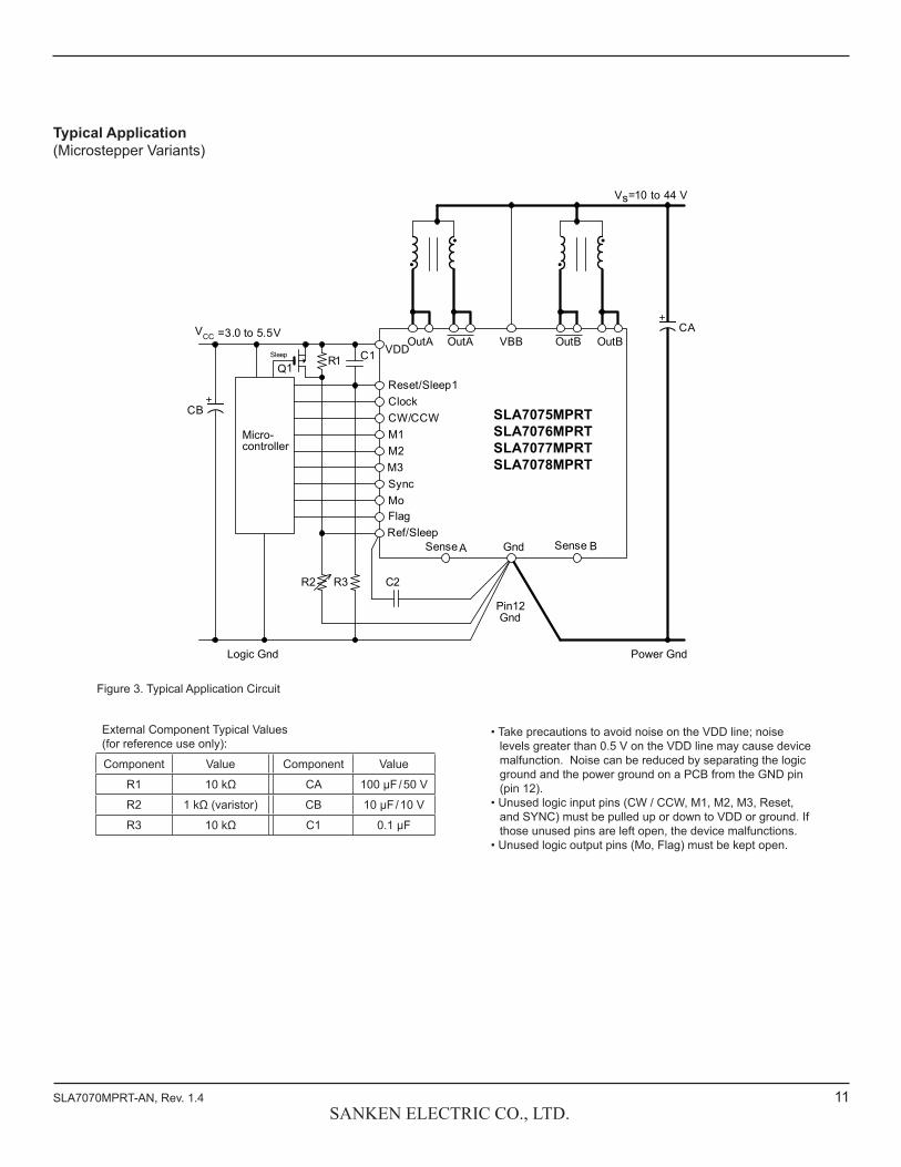
Typical Application(Microstepper Variants)
External Component Typical Values(for reference use only):
Component Value Component Value
R1 10 kΩ CA 100 μF / 50 V
R2 1 kΩ (varistor) CB 10 μF / 10 V
R3 10 kΩ C1 0.1 μF
• Take precautions to avoid noise on the VDD line; noise levels greater than 0.5 V on the VDD line may cause device malfunction. Noise can be reduced by separating the logic ground and the power ground on a PCB from the GND pin (pin 12).
• Unused logic input pins (CW / CCW, M1, M2, M3, Reset, and SYNC) must be pulled up or down to VDD or ground. If those unused pins are left open, the device malfunctions.
• Unused logic output pins (Mo, Flag) must be kept open.
Figure 3. Typical Application Circuit
12SANKEN ELECTRIC CO., LTD.
SLA7070MPRT-AN, Rev. 1.4
Truth TablesCommon Input PinsTable 1 shows the truth table for input pins common to both half/full step and microstep variants of the SLA7070MPRT series.
• The Reset function is asynchronous. If the input on the Reset pin is high, the internal logic circuit is reset. At this point, if the Ref pin stays low, then the DMOS outputs turn on at the starting point of excitation. Note that the Disable control functions are not available with the Reset pin signal set high.
• Voltage at the Ref / Sleep1 pin controls the PWM current and the Sleep1 function. For normal operation, VREF should be below 1.5 V (low level). Applying a voltage greater than 2.0 V (high level) to the Ref / Sleep1 pin disables the outputs and puts the motor in a free state (coast). This function is used to minimize power consumption when the device is not in use. Although it disables much of the internal circuitry, including the out-put MOSFETs and regulator, the sequencer / translator circuit remains active.
• The Sync function is active only for 2-phase excitation timing. If this function is used during other than 2-phase excitation tim-ing, the overall stepping sequence might collapse because PWM off-time and set current are different in each phase A and phase B control scenario. (2-phase excitation timing is when the step reference current ratio of both phase A and phase B is Mode 8.)
Commutation/Sleep2 FunctionTable 2 shows the logic of the pins (M1, M2, and M3) which set commutation. In the Sleep2 function, the outputs are disabled and the driver supply current (IBB) is reduced. However, unlike the Sleep1 function, the logic circuitry is put into a standby state and therefore the sequencer / translator circuit is not active.
Note: When awakening from Sleep2 mode, a delay of 100 μs or longer before sending a Clock pulse is recommended.
Monitor Output PinThe SLA7070MPRT series provides two device status monitor outputs:
• Flag pin – Protection feature operation• Mo pin (microstep variants only) – Stepping sequenceTable 3 shows the logic for the monitor pins. The outputs turn off when the protection circuit starts operating. To release the protec-tion state, cycle (set low, and then high) the logic supply voltage (VDD).
Table 1. Truth Table for Common Input Pins (Half/Full and Microstep)Pin Name Low Level High Level Clock
Reset Normal operation Logic reset
(Positive Edge)
CW/CCW Forward (CW) Reverse (CCW)
M1, M2, M3 Commutation (Sleep2 is not included)
Ref / Sleep1 Normal operation Sleep1 function
Sync Non-sync PWM control Sync PWM control
Table 2. Commutation-Sleep2 Truth Table for Common Input Pins (Half/Full and Microstep)
Pin NameFull / Half Step Microstep
M1 M2 M3L L L Full step (Mode 8 fixed) Full step (Mode 8 fixed)
H L L Full step (Mode F fixed) Full step (Mode F fixed)
L H L Half step Half step
H H L Half step (Mode F fixed) Half step (Mode F fixed)
L L H
Sleep2 function
Quarter step
H L H Eighth step
L H H Sixteenth step
H H H Sleep2 function
Table 3. Monitor Output Pins Logic Pin Name Low Level High Level
Flag Normal operation Protection circuit operation
Mo Other than 2-phase excitation timing 2-phase excitation timing
13SANKEN ELECTRIC CO., LTD.
SLA7070MPRT-AN, Rev. 1.4
Logic Input PinsThe low pass filter incorporated with the logic input pins (Reset, Clock, CW/CCW, M1, M2, M3, and Sync) improves noise rejec-tion. The logic inputs are CMOS input compatible, and therefore they are in a high impedance state. Use the IC at a fixed input level, either low or high.
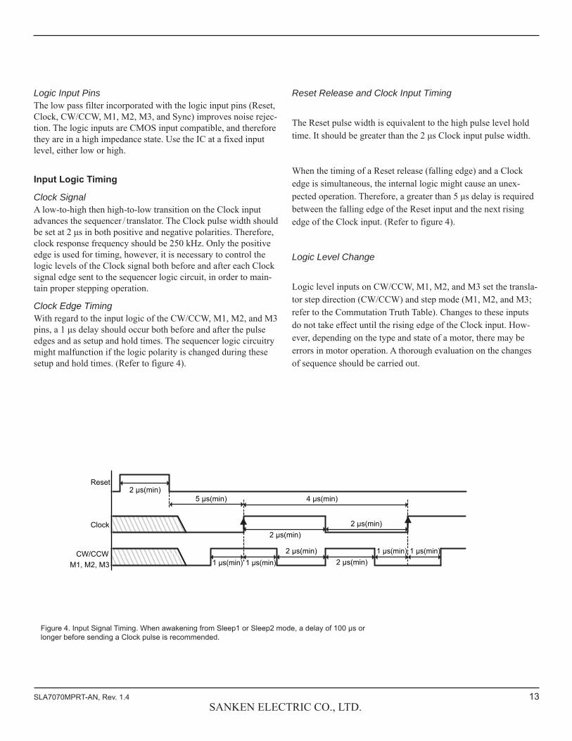
Input Logic Timing
Clock SignalA low-to-high then high-to-low transition on the Clock input advances the sequencer / translator. The Clock pulse width should be set at 2 μs in both positive and negative polarities. Therefore, clock response frequency should be 250 kHz. Only the positive edge is used for timing, however, it is necessary to control the logic levels of the Clock signal both before and after each Clock signal edge sent to the sequencer logic circuit, in order to main-tain proper stepping operation.
Clock Edge TimingWith regard to the input logic of the CW/CCW, M1, M2, and M3 pins, a 1 μs delay should occur both before and after the pulse edges and as setup and hold times. The sequencer logic circuitry might malfunction if the logic polarity is changed during these setup and hold times. (Refer to figure 4).
Reset Release and Clock Input Timing
The Reset pulse width is equivalent to the high pulse level hold time. It should be greater than the 2 μs Clock input pulse width.
When the timing of a Reset release (falling edge) and a Clock edge is simultaneous, the internal logic might cause an unex-pected operation. Therefore, a greater than 5 μs delay is required between the falling edge of the Reset input and the next rising edge of the Clock input. (Refer to figure 4).
Logic Level Change
Logic level inputs on CW/CCW, M1, M2, and M3 set the transla-tor step direction (CW/CCW) and step mode (M1, M2, and M3; refer to the Commutation Truth Table). Changes to these inputs do not take effect until the rising edge of the Clock input. How-ever, depending on the type and state of a motor, there may be errors in motor operation. A thorough evaluation on the changes of sequence should be carried out.
Figure 4. Input Signal Timing. When awakening from Sleep1 or Sleep2 mode, a delay of 100 μs or longer before sending a Clock pulse is recommended.
Reset2 μs(min)
2 μs(min)2 μs(min)
2 μs(min)1 μs(min) 1 μs(min)
1 μs(min) 1 μs(min)2 μs(min)
5 μs(min) 4 μs(min)
Clock
CW/CCWM1, M2, M3
14SANKEN ELECTRIC CO., LTD.
SLA7070MPRT-AN, Rev. 1.4
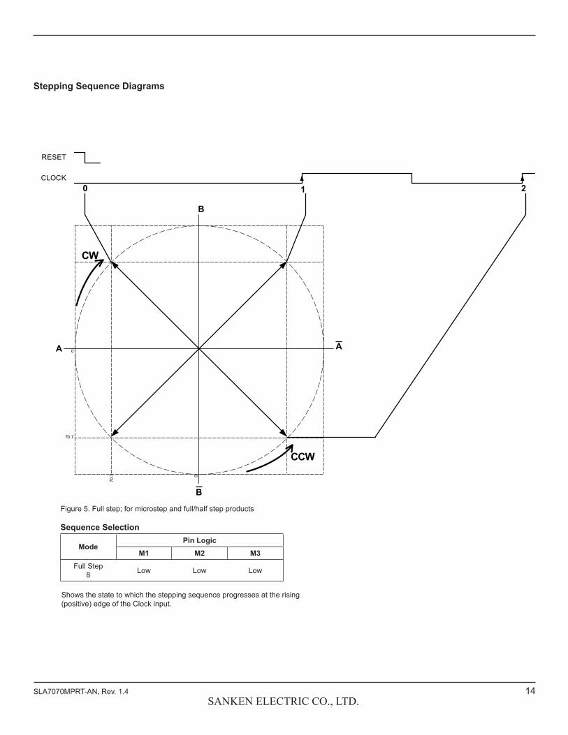
Figure 5. Full step; for microstep and full/half step products
Sequence Selection
ModePin Logic
M1 M2 M3Full Step
8 Low Low Low
Shows the state to which the stepping sequence progresses at the rising (positive) edge of the Clock input.
A
B
B
A
0 1 2
70.7
0
70.7 0
RESET
CLOCK
CW
CCW
Stepping Sequence Diagrams
15SANKEN ELECTRIC CO., LTD.
SLA7070MPRT-AN, Rev. 1.4
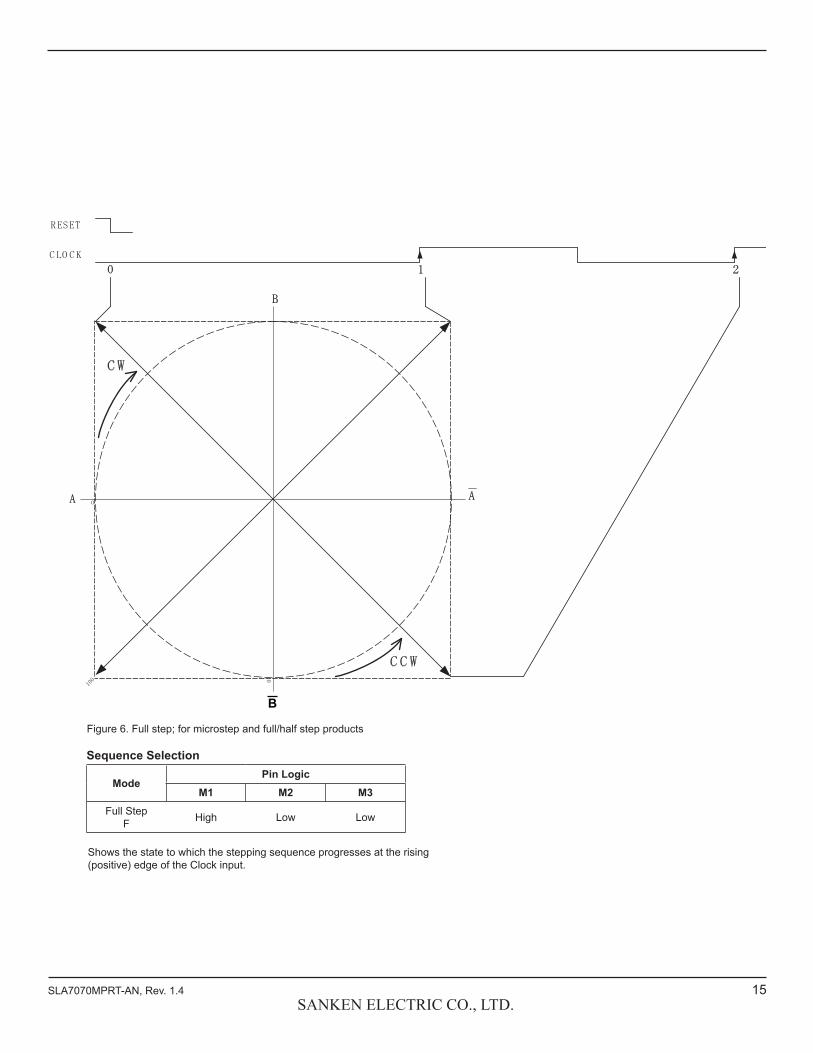
Figure 6. Full step; for microstep and full/half step products
Sequence Selection
ModePin Logic
M1 M2 M3Full Step
F High Low Low
B
Shows the state to which the stepping sequence progresses at the rising (positive) edge of the Clock input.
16SANKEN ELECTRIC CO., LTD.
SLA7070MPRT-AN, Rev. 1.4
Figure 7. Half step; for microstep and full/half step products
Sequence Selection
ModePin Logic
M1 M2 M3Half Step
8, F Low High Low
A
B
B
A
0 1 2 3 4
100
70.7
0
70.7 0
RESET
CLOCK
CW
CCW
Shows the state to which the stepping sequence progresses at the rising (positive) edge of the Clock input.
17SANKEN ELECTRIC CO., LTD.
SLA7070MPRT-AN, Rev. 1.4
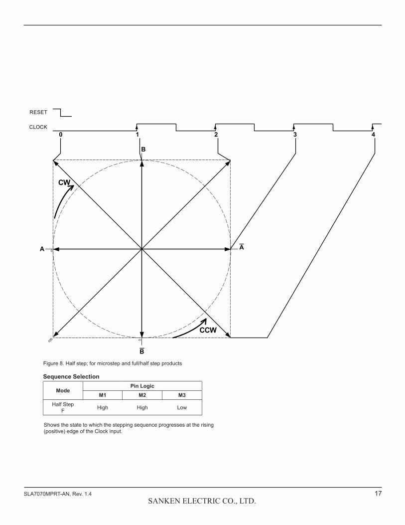
Figure 8. Half step; for microstep and full/half step products
Sequence Selection
ModePin Logic
M1 M2 M3Half Step
F High High Low
A
B
B
A
0 1 2 3 4
100
0
0
RESET
CLOCK
CW
CCW
Shows the state to which the stepping sequence progresses at the rising (positive) edge of the Clock input.
18SANKEN ELECTRIC CO., LTD.
SLA7070MPRT-AN, Rev. 1.4
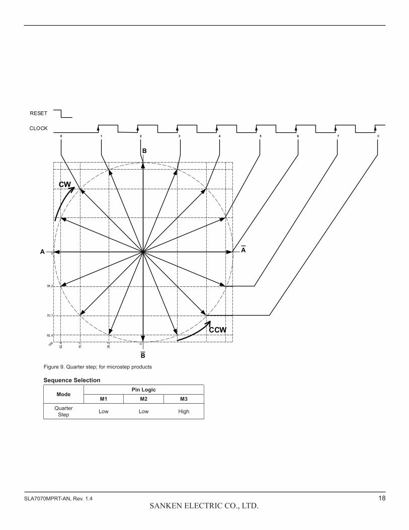
Figure 9. Quarter step; for microstep products
Sequence Selection
ModePin Logic
M1 M2 M3Quarter
Step Low Low High
A
B
B
A
0 1 2 3 4 5 6 7 8
92.4
100
70.7
38.2
0
70.7
38.2 0
92.4
RESET
CLOCK
CW
CCW
19SANKEN ELECTRIC CO., LTD.
SLA7070MPRT-AN, Rev. 1.4
Figure 10. Eighth step; for microstep products
Sequence Selection
ModePin Logic
M1 M2 M3EighthStep High Low High
A
B
B
A
0 1 2 3 4 5 6 7 8 9 10
11
12
13
14
15
16
98.192.4
100
98.1
83.1
70.7
55.5
38.2
19.5
0
83.1
70.7
55.5
38.2
19.5 0
92.4
RESET
CLOCK
CW
CCW
Shows the state to which the stepping sequence progresses at the rising (positive) edge of the Clock input.
20SANKEN ELECTRIC CO., LTD.
SLA7070MPRT-AN, Rev. 1.4
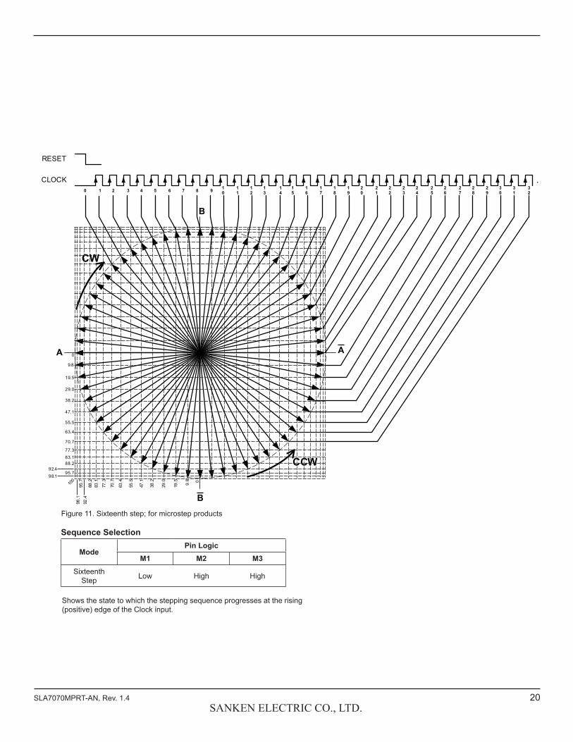
Figure 11. Sixteenth step; for microstep products
Sequence Selection
ModePin Logic
M1 M2 M3Sixteenth
Step Low High High
A
B
B
A
98.192.4
95.7
100
98.1
95.7
88.283.177.3
70.7
63.4
55.5
47.1
38.2
29.0
19.5
9.8
0
88.2
83.1
77.3
70.7
63.4
55.5
47.1
38.2
29.0
19.5 9.8 0
92.4
CW
CCW
10 2 3 4 65 7 8 9 10
11
12
13
15
14
16
17
18
19
20
21
22
23
24
25
26
27
28
29
30
31
32
…
RESET
CLOCK
Shows the state to which the stepping sequence progresses at the rising (positive) edge of the Clock input.
21SANKEN ELECTRIC CO., LTD.
SLA7070MPRT-AN, Rev. 1.4
Table 4. Excitation Mode States
DirectionInternal Sequence State Step Sequencing
Phase A Phase B Full Step Half Step 1/4 Step 1/8 Step 1/16 StepPWM Mode PWM Mode Mode 8 Mode F Mode 8, F Mode F
CounterClockwise
Clockwise
A 8 B 8 X X* X X* X X XA 7 B 9 XA 6 B A X XA 5 B B XA 4 B C X X XA 3 B D XA 2 B E X XA 1 B F X– – B F X X X X X A 1 B F X A 2 B E X X A 3 B D X A 4 B C X X X A 5 B B X A 6 B A X X A 7 B 9 X A 8 B 8 X X* X X* X X X A 9 B 7 X A A B 6 X X A B B 5 X A C B 4 X X X A D B 3 X A E B 2 X X A F B 1 X A F – – X X X X X A F B 1 X A E B 2 X X A D B 3 X A C B 4 X X X A B B 5 X A A B 6 X X A 9 B 7 X A 8 B 8 X X* X X* X X X A 7 B 9 X A 6 B A X X A 5 B B X A 4 B C X X X A 3 B D X A 2 B E X X A 1 B F X– – B F X X X X XA 1 B F XA 2 B E X XA 3 B D XA 4 B C X X XA 5 B B XA 6 B A X XA 7 B 9 XA 8 B 8 X X* X X* X X XA 9 B 7 XA A B 6 X XA B B 5 XA C B 4 X X XA D B 3 XA E B 2 X XA F B 1 XA F – – X X X X XA F B 1 XA E B 2 X XA D B 3 XA C B 4 X X XA B B 5 XA A B 6 X XA 9 B 7 X
Sequence state is Mode 8, but step reference current ratio is Mode F. Mode F has step reference current ratio of 100%, and PWM off-time of 12 μs.
Excitation Change SequenceThe change of excitation modes is determined by the settings of the excitation pins (M1, M2, and M3) before and after the step signal.Table 4 shows each excitation mode state setting.
22SANKEN ELECTRIC CO., LTD.
SLA7070MPRT-AN, Rev. 1.4
Individual Circuit Descriptions
Monolithic IC (MIC)• Sequencer Logic The single Clock input is used for step tim-ing. Direction is controlled by the CW/CCW input. Commutation mode is controlled by the combination of the M1, M2, and M3 inputs logic levels. For details, refer to the Commutation Truth Table.
• PWM Control Each pair of outputs is controlled by a fixed off-time PWM current-control circuit. The internal oscillator (OSC) sets the off-time. Its operation mechanism is identical to that of the SLA7070M family. Refer to the PWM Current Control sec-tion for further details.
• Synchronous Control This function prevents occasional motor noise during Hold mode, which normally results from asynchronous PWM operation of both motor phases. A logic high at the Sync input sets synchronous operation. A logic low sets asynchronous operation. The use of synchronous operation during normal stepping is not recommended because it produces less motor torque and can cause motor vibration due to staircase current. The use of synchronous operation when the motor is not in operation is allowed only in full/half step sequence timing, due to the difference in the current controlled and PWM off-time at other step sequence timings.
• DAC (D-to-A Converter) In microstep sequencing, the cur-rent at each step is set by the value of a sense resistor (RSInt), a reference voltage (VREF), and the output voltage of the DACs, controlled by the output of the sequencer / translator). Please refer the electric characteristic, Step Reference Current Ratio, page 8.
• Regulator Circuit The integrated regulator circuit is used in driving the output MOSFET gates and powering other internal linear circuits.
• Protect Circuit A built-in protection circuit against motor coil opens or shorts is provided. Protection is activated by sensing voltage on the internal RSInt resistors; therefore, an overcurrent condition cannot be detected which results from the the Outx pins or Sensex pins, or both, shorting to Gnd. Protection against motor coil opens is available only during PWM operation; therefore, it does not work at constant voltage driving, when the motor is rotating at high speed. Operation of the protection circuit disables all of the DMOS outputs. To come out of protection mode, cycle the logic supply, VDD .
• TSD circuit This circuit protects a driver by shifting the output to Disable mode when the temperature of a product control IC (MIC) rises and becomes higher than threshold value. In order to reset, cycle the logic supply, VDD .
Output MOSFET ChipThe value of the built-in output DMOS chip varies according to which of the four different output current ratings has been selected.
Sense ResistorThe resistance varies according to which of the four different output current ratings has been selected, as follows:
Output Current(A)
RSInt Resistance(Ω typ)
1 0.305
1.5 0.305
2 0.205
3 0.155
Each resistance shown above includes the inherent resistance (approximately 5 mΩ) in the resistor itself.
23SANKEN ELECTRIC CO., LTD.
SLA7070MPRT-AN, Rev. 1.4
PWM Current ControlBlanking TimeThe actual operating waveforms on the Sensex pins when driving a motor are shown in figure 12. The actual operating waveforms on the Sensex pins when driving a motor are shown in figure 13. Immediately after PWM turns OFF, ringing (or spike) noise on the Sensex pins isobserved for a few μs. Ringing noise can be generated by various causes, such as capacitance between motor coils and inappropriate motor wiring.
Each pair of outputs is controlled by a fixed off-time (7 to 12 μs, depending on stepping mode) PWM current-control circuit that limits the load current to a target value, ITRIP . Initially, an output is enabled and current flows through the motor winding and the current-sense resistors. When the voltage across the current sense resistor equals the DAC output voltage, VTRIP , the current sense comparator resets the PWM latch. This turns off the driver for the fixed off-time, during which the load inductance causes the cur-rent to recirculate for the off-time period. Therefore, if the ringing noise on the sense resistor equals and surpasses VTRIP , PWM turns off.
To prevent this phenomenon, the blanking time is set to override signals from the current-sense comparator for a certain period immediately after PWM turns on.
Functional Description
ITRIP
5 μs/div
ITRIP
500 ns/div
Figure 12. Operating waveforms on the Sensex pins during PWM chopping (circled area of left panel is shown in expanded scale in right panel)
Figure 13. Sensex pin waveform during PWM control
tON
Blanking Time
A
A
0
ITRIP
tOFF(Fixed)
PWM Pulse Width
24SANKEN ELECTRIC CO., LTD.
SLA7070MPRT-AN, Rev. 1.4
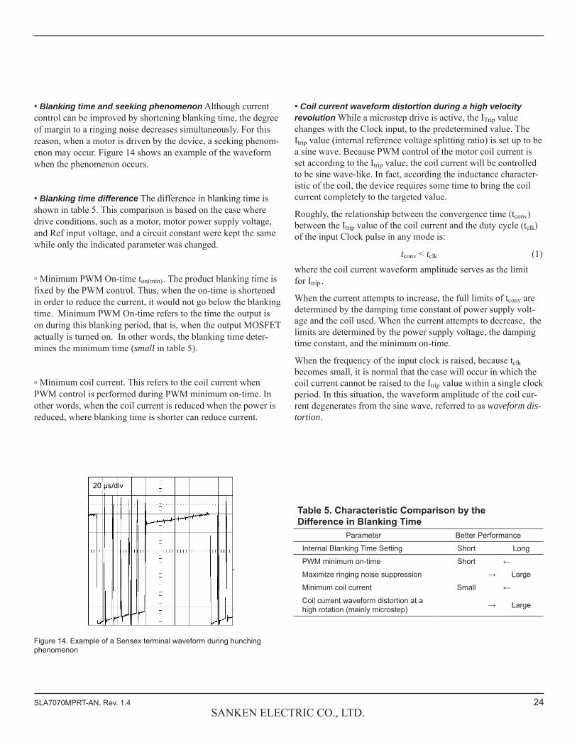
• Blanking time and seeking phenomenon Although current control can be improved by shortening blanking time, the degree of margin to a ringing noise decreases simultaneously. For this reason, when a motor is driven by the device, a seeking phenom-enon may occur. Figure 14 shows an example of the waveform when the phenomenon occurs.
• Blanking time difference The difference in blanking time is shown in table 5. This comparison is based on the case where drive conditions, such as a motor, motor power supply voltage, and Ref input voltage, and a circuit constant were kept the same while only the indicated parameter was changed.
▫ Minimum PWM On-time ton(min) . The product blanking time is fixed by the PWM control. Thus, when the on-time is shortened in order to reduce the current, it would not go below the blanking time. Minimum PWM On-time refers to the time the output is on during this blanking period, that is, when the output MOSFET actually is turned on. In other words, the blanking time deter-mines the minimum time (small in table 5).
▫ Minimum coil current. This refers to the coil current when PWM control is performed during PWM minimum on-time. In other words, when the coil current is reduced when the power is reduced, where blanking time is shorter can reduce current.
• Coil current waveform distortion during a high velocity revolution While a microstep drive is active, the ITrip value changes with the Clock input, to the predetermined value. The Itrip value (internal reference voltage splitting ratio) is set up to be a sine wave. Because PWM control of the motor coil current is set according to the Itrip value, the coil current will be controlled to be sine wave-like. In fact, according the inductance character-istic of the coil, the device requires some time to bring the coil current completely to the targeted value.
Roughly, the relationship between the convergence time (tconv) between the Itrip value of the coil current and the duty cycle (tclk) of the input Clock pulse in any mode is:
tconv < tclk (1)
where the coil current waveform amplitude serves as the limit for Itrip .
When the current attempts to increase, the full limits of tconv are determined by the damping time constant of power supply volt-age and the coil used. When the current attempts to decrease, the limits are determined by the power supply voltage, the damping time constant, and the minimum on-time.
When the frequency of the input clock is raised, because tclk becomes small, it is normal that the case will occur in which the coil current cannot be raised to the Itrip value within a single clock period. In this situation, the waveform amplitude of the coil cur-rent degenerates from the sine wave, referred to as waveform dis-tortion.
20 μs/div
Figure 14. Example of a Sensex terminal waveform during hunching phenomenon
Table 5. Characteristic Comparison by the Difference in Blanking Time
Parameter Better Performance
Internal Blanking Time Setting Short Long
PWM minimum on-time Short ←
Maximize ringing noise suppression → Large
Minimum coil current Small ←
Coil current waveform distortion at a high rotation (mainly microstep) → Large
25SANKEN ELECTRIC CO., LTD.
SLA7070MPRT-AN, Rev. 1.4
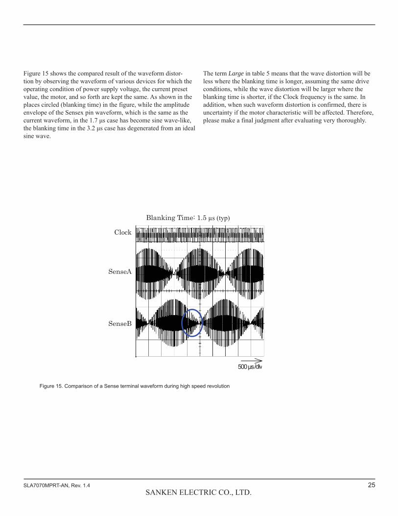
Figure 15 shows the compared result of the waveform distor-tion by observing the waveform of various devices for which the operating condition of power supply voltage, the current preset value, the motor, and so forth are kept the same. As shown in the places circled (blanking time) in the figure, while the amplitude envelope of the Sensex pin waveform, which is the same as the current waveform, in the 1.7 μs case has become sine wave-like, the blanking time in the 3.2 μs case has degenerated from an ideal sine wave.
The term Large in table 5 means that the wave distortion will be less where the blanking time is longer, assuming the same drive conditions, while the wave distortion will be larger where the blanking time is shorter, if the Clock frequency is the same. In addition, when such waveform distortion is confirmed, there is uncertainty if the motor characteristic will be affected. Therefore, please make a final judgment after evaluating very thoroughly.
500 μs/div
SenseA
SenseB
1.5 typ(Blanking Time: 1.5 μs (typ)
Clock
Figure 15. Comparison of a Sense terminal waveform during high speed revolution
26SANKEN ELECTRIC CO., LTD.
SLA7070MPRT-AN, Rev. 1.4
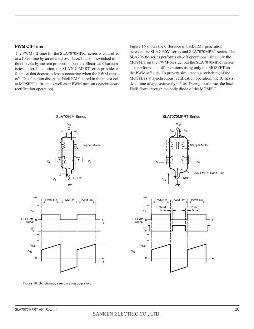
PWM Off-Time The PWM off-time for the SLA7070MPRT series is controlled at a fixed time by an internal oscillator. It also is switched in three levels by current proportion (see the Electrical Character-istics table). In addition, the SLA7070MPRT series provides a function that decreases losses occurring when the PWM turns off. This function dissipates back EMF stored in the motor coil at MOSFET turn-on, as well as at PWM turn-on (synchronous rectification operation).
Figure 16 shows the difference in back EMF generation between the SLA7060M series and SLA7070MPRT series. The SLA7060M series performs on–off operations using only the MOSFET on the PWM-on side, but the SLA7070MPRT series also performs on–off operations using only the MOSFET on the PWM-off side. To prevent simultaneous switching of the MOSFETs at synchronous rectification operation, the IC has a dead time of approximately 0.5 μs. During dead time, the back EMF flows through the body diode of the MOSFET.
Figure 16. Synchronous rectification operation
SLA7060M Series SLA7070MPRT Series
VBB
RSExt RSIntVS
VS VS
FET GateSignal
FET GateSignal
Vg
Stepper Motor Stepper Motor
VBB
IoffIonIoffIon
VS
VgVg Vg
Vg Vg
PWM On PWM Off PWM On
Back EMF at Dead Time
Vg
+V
VREF
0t
Vg
+V
VREF
0
0 0
t
t t
PWM On PWM Off PWM On
Dead Time
DeadTime
27SANKEN ELECTRIC CO., LTD.
SLA7070MPRT-AN, Rev. 1.4
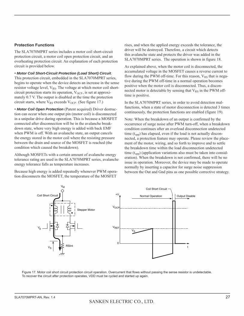
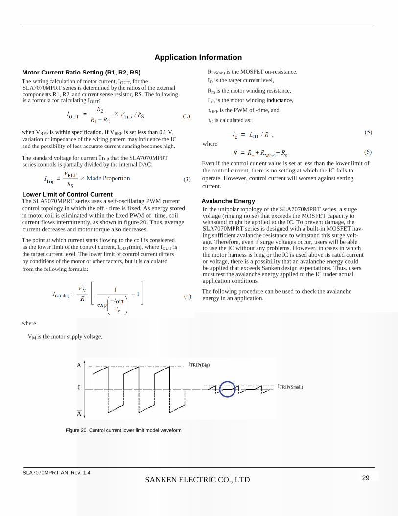
Protection FunctionsThe SLA7070MPRT series includes a motor coil short-circuit protection circuit, a motor coil open protection circuit, and an overheating protection circuit. An explanation of each protection circuit is provided below.
• Motor Coil Short-Circuit Protection (Load Short) Circuit. This protection circuit, embedded in the SLA7070MPRT series, begins to operate when the device detects an increase in the sense resistor voltage level, VRS. The voltage at which motor coil short-circuit protection starts its operation, VOCP , is set at approxi-mately 0.7 V. The output is disabled at the time the protection circuit starts, where VRS exceeds VOCP . (See figure 17.)
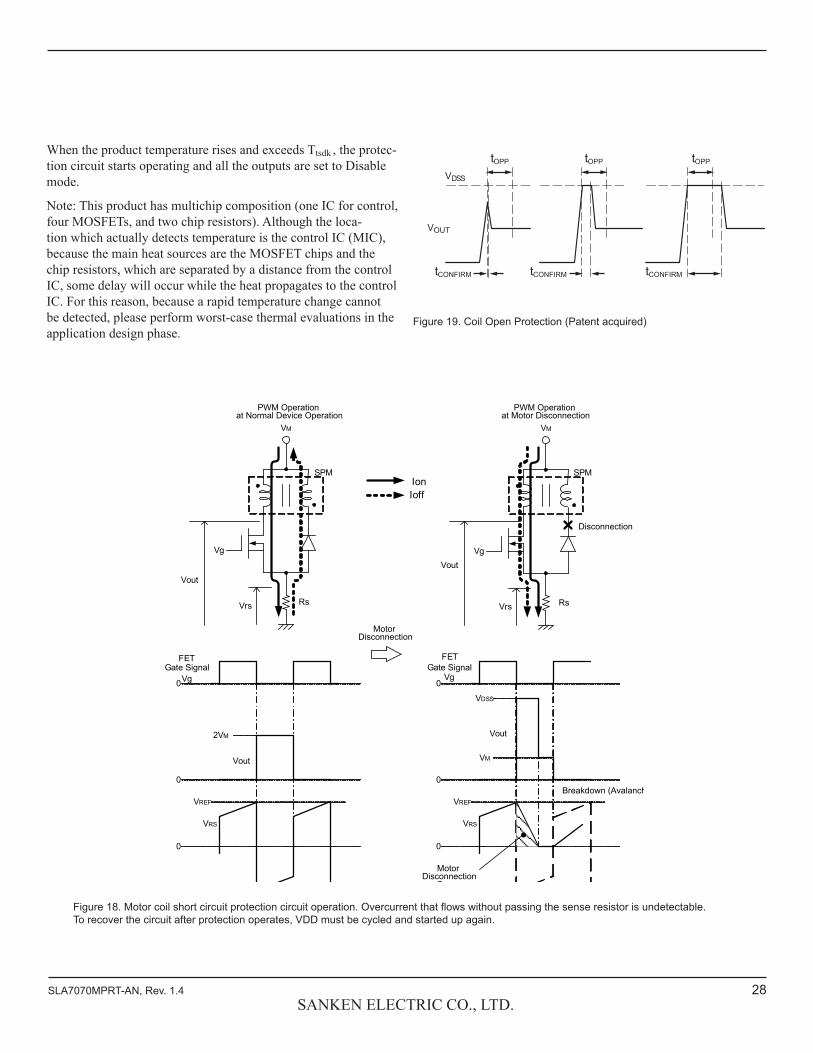
• Motor Coil Open Protection (Patent acquired) Driver destruc-tion can occur when one output pin (motor coil) is disconnected in a unipolar drive during operation. This is because a MOSFET connected after disconnection will be in the avalanche break-down state, where very high energy is added with back EMF when PWM is off. With an avalanche state, an output cancels the energy stored in the motor coil where the resisting pressure between the drain and source of the MOSFET is reached (the condition which caused the breakdown).
Although MOSFETs with a certain amount of avalanche energy tolerance rating are used in the SLA7070MPRT series, avalanche energy tolerance falls as temperature increases.
Because high energy is added repeatedly whenever PWM opera-tion disconnects the MOSFET, the temperature of the MOSFET
rises, and when the applied energy exceeds the tolerance, the driver will be destroyed. Therefore, a circuit which detects this avalanche state and protects the driver was added in the SLA7070MPRT series. The operation is shown in figure 18.
As explained above, when the motor coil is disconnected, the accumulated voltage in the MOSFET causes a reverse current to flow during the PWM off-time. For this reason, VRS that is nega-tive during the PWM off-time in a normal operation becomes positive when the motor coil is disconnected. Thus, a discon-nected motor is detectable by sensing that VRS in the PWM off-time is positive.
In the SLA7070MPRT series, in order to avoid detection mal-functions, when a state of motor disconnection is detected 3 times continuously, the protection functions are enabled (figure 19).
Note: When the breakdown of an output is confirmed by the occurrence of surge noise after PWM turn-off, when a breakdown condition continues after an overload disconnection undetected time (topp) has elapsed, even if the load is not actually discon-nected, a protection feature may operate. Please review the place-ment of the motor, wiring, and so forth to improve and to settle the breakdown time within the load disconnection undetected time (topp) (application variations also must be taken into consid-eration). When the breakdown is not confirmed, there will be no issue in operation. Moreover, the device may be made to operate normally by inserting a capacitor for surge noise suppression between the Out and Gnd pins as one possible corrective strategy.
Stepper Motor
Coil Short Circuit
Coil Short Circuit
Normal Operation Output Disable
VM
VOCP
+V
VREF
0tRSIntVS
VSVg
Figure 17. Motor coil short circuit protection circuit operation. Overcurrent that flows without passing the sense resistor is undetectable. To recover the circuit after protection operates, VDD must be cycled and started up again.
28SANKEN ELECTRIC CO., LTD.
SLA7070MPRT-AN, Rev. 1.4
When the product temperature rises and exceeds Ttsdk , the protec-tion circuit starts operating and all the outputs are set to Disable mode.
Note: This product has multichip composition (one IC for control, four MOSFETs, and two chip resistors). Although the loca-tion which actually detects temperature is the control IC (MIC), because the main heat sources are the MOSFET chips and the chip resistors, which are separated by a distance from the control IC, some delay will occur while the heat propagates to the control IC. For this reason, because a rapid temperature change cannot be detected, please perform worst-case thermal evaluations in the application design phase.
Figure 18. Motor coil short circuit protection circuit operation. Overcurrent that flows without passing the sense resistor is undetectable. To recover the circuit after protection operates, VDD must be cycled and started up again.
0
0
2VM
VREF
Vout
VRS
0
0
VM
VREF
Vout
VRS
VDSS
0 0
FET Gate Signal Gate Signal
Breakdown (Avalanch
Vg
FET
Vg
Vg
SPM
PWM Operation at Normal Device Operation
PWM Operation at Motor Disconnection
Disconnection
Motor Disconnection
Motor Disconnection
S
Vout
Vrs Rs
Vg
SPM
Vout
Vrs Rs
IonIoff
VM VM
tOPP
tCONFIRM tCONFIRM tCONFIRM
tOPP tOPP
VOUT
VDSS
Figure 19. Coil Open Protection (Patent acquired)
A
0
A
Application Information
Motor Current Ratio Setting (R1, R2, RS)
The setting calculation of motor current, IOUT, for the
SLA7070MPRT series is determined by the ratios of the external
components R1, R2, and current sense resistor, RS. The following
is a formula for calculating IOUT:
when VREF is within specification. If VREF is set less than 0.1 V,
variation or impedance of the wiring pattern may influence the IC
and the possibility of less accurate current sensing becomes high.
The standard voltage for current ITrip that the SLA7070MPRT series controls is partially divided by the internal DAC:
Lower Limit of Control Current The SLA7070MPRT series uses a self-oscillating PWM current
control topology in which the off - time is fixed. As energy stored
in motor coil is eliminated within the fixed PWM of -time, coil
current flows intermittently, as shown in figure 20. Thus, average
current decreases and motor torque also decreases.
The point at which current starts flowing to the coil is considered
as the lower limit of the control current, IOUT(min), where IOUT is
the target current level. The lower limit of control current differs
by conditions of the motor or other factors, but it is calculated
from the following formula:
RDS(on) is the MOSFET on-resistance,
IO is the target current level,
Rm is the motor winding resistance,
Lm is the motor winding inductance,
tOFF is the PWM of -time, and
tC is calculated as:
where
Even if the control cur ent value is set at less than the lower limit of
the control current, there is no setting at which the IC fails to
operate. However, control current will worsen against setting
current.
Avalanche Energy
In the unipolar topology of the SLA7070MPRT series, a surge voltage (ringing noise) that exceeds the MOSFET capacity to
withstand might be applied to the IC. To prevent damage, the SLA7070MPRT series is designed with a built-in MOSFET hav- ing sufficient avalanche resistance to withstand this surge volt- age. Therefore, even if surge voltages occur, users will be able to use the IC without any problems. However, in cases in which the motor harness is long or the IC is used above its rated current or voltage, there is a possibility that an avalanche energy could be applied that exceeds Sanken design expectations. Thus, users must test the avalanche energy applied to the IC under actual application conditions.
The following procedure can be used to check the avalanche
energy in an application.
where
VM is the motor supply voltage,
ITRIP(Big)
ITRIP(Small)
Figure 20. Control current lower limit model waveform
SLA7070MPRT-AN, Rev. 1.4
SANKEN ELECTRIC CO., LTD 29
30SANKEN ELECTRIC CO., LTD.
SLA7070MPRT-AN, Rev. 1.4
Given:
From the waveform test result (reference figure 22)
VDS(AV) = 140 V,ID = 1 A, andt = 0.5 μs.
The avalanche energy, EAV can be calculated using the following:
VDS(AV) ID1/2
1/2
EAV=
==
t
140 (V)
0.035 (mJ)
1 (A) 0.5 10-6 (µs)
(7)
By comparing the EAV calculated with the graph shown in fig-ure 23, the application can be evaluated if it is safe for the IC, by being within the avalanche energy-tolerated does range of the MOSFET.
On-Off Sequence of Power Supply (VBB and VDD)There is no restriction of the on-off sequence between the main power supply, VBB, and the logic supply, VDD.
0
4
8
12
16
20
0 25 50 75 100 125 150
EA
V [m
J]
Product Temperature, Tc [°C]
SLA7073M and SLA7078M
SLA7070M andSLA7075M
SLA7071M andSLA7076M
SLA7072M and SLA7077M
Stepper Motor
RSInt
VM
I D
VD S(A V )
Figure 21. Test points
Figure 22. Waveform at avalanche breakdown
Figure 23. SLA7070MPRT iterated avalanche energy tolerated level, EAV(max)
31SANKEN ELECTRIC CO., LTD.
SLA7070MPRT-AN, Rev. 1.4
Motor Supply Voltage (VM) and Main Power Supply Voltage (VBB)Because the SLA7070MPRT series has a structure that sepa-rates the control IC (MIC) and the power MOSFETs as shown in the Functional Block diagrams, the motor supply and main power supply are separated. Therefore, it is possible to drive the IC using different power supplies and different voltages for motor supply and main power supply. However, extra caution is required because the supply voltage ranges differ among power supplies.
Internal Logic CircuitsResetThe sequencer/translator circuit of this product is initialized after logic supply (VDD) is applied, and the power-on reset function operates. To initialize the sequencer/translator, the output imme-diately after power-on indicates the status that the power circuits are in the home state. In a case where the sequencer/translator must be reset after the motor has been operating, a reset signal must be input on the Reset pin. In a case in which external reset control is not necessary, and the Reset pin is not used, the Reset pin must be pulled to logic low on the application circuit board.
Clock InputWhen the Clock input signal stops, excitation changes to the motor Hold state. At this time, there is no difference to the IC if the Clock input signal is at the low level or the high level. The SLA7070MPRT series is designed to move one sequence incre-ment at a time, according to the current stepping mode, when a positive Clock pulse edge is detected.
Chopping Synchronous CircuitThe SLA7070MPRT series has a chopping synchronous func-tion to protect from abnormal noises that may occasionally occur during the motor Hold state. This function can be operated by setting the Sync pin at high level. However, if this function is used during motor rotation, control current does not stabilize, and therefore this may cause reduction of motor torque or increased vibration. So, Sanken does not recommend using this function while the motor is rotating. In addition, the synchronous circuit should be disabled in order to control motor current properly in case it is used other than in dual excitation state (Modes 8 and F) or single excitation Hold state.
In normal operation, generally the input signal for switching can be sent from an external microcomputer. However, in applica-tions where the input signal cannot be transmitted adequately due to limitations of the port, the following method can be taken to use the functions.
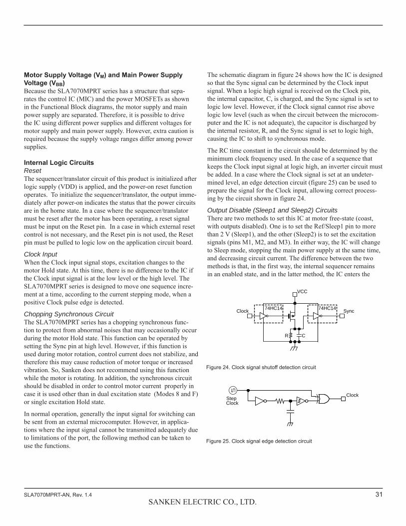
The schematic diagram in figure 24 shows how the IC is designed so that the Sync signal can be determined by the Clock input signal. When a logic high signal is received on the Clock pin, the internal capacitor, C, is charged, and the Sync signal is set to logic low level. However, if the Clock signal cannot rise above logic low level (such as when the circuit between the microcom-puter and the IC is not adequate), the capacitor is discharged by the internal resistor, R, and the Sync signal is set to logic high, causing the IC to shift to synchronous mode.
The RC time constant in the circuit should be determined by the minimum clock frequency used. In the case of a sequence that keeps the Clock input signal at logic high, an inverter circuit must be added. In a case where the Clock signal is set at an undeter-mined level, an edge detection circuit (figure 25) can be used to prepare the signal for the Clock input, allowing correct process-ing by the circuit shown in figure 24.
Output Disable (Sleep1 and Sleep2) CircuitsThere are two methods to set this IC at motor free-state (coast, with outputs disabled). One is to set the Ref/Sleep1 pin to more than 2 V (Sleep1), and the other (Sleep2) is to set the excitation signals (pins M1, M2, and M3). In either way, the IC will change to Sleep mode, stopping the main power supply at the same time, and decreasing circuit current. The difference between the two methods is that, in the first way, the internal sequencer remains in an enabled state, and in the latter method, the IC enters the
Clock Sync
VCC
74HC1474HC14
R C
Figure 24. Clock signal shutoff detection circuit
Figure 25. Clock signal edge detection circuit
StepClock
Clock
32SANKEN ELECTRIC CO., LTD.
SLA7070MPRT-AN, Rev. 1.4
Hold state. Moreover, in the method using the excitation signals (Sleep2), excitation timing remains in a standby state, even if a signal is input on the Clock pin during Sleep mode.
When awaking to normal operating mode (motor rotation) from Disable (Sleep1 or Sleep2) mode, set an appropriate delay time from cancellation of the Disable mode to the initial Clock input edge. In doing so, consider not only the rise time for the IC, but also the rise time for the motor excitation current, which is important (see figure 26).
Ref/Sleep1 PinThe Ref/Sleep1 pin provides access to the following functions:
• Standard voltage setting for output current level setting
• Output Enable-Disable control input
These functions are further described in the Truth Table section, and in the discussion of output disabling, above.
Range A. In this range, control current value also varies in accordance with VREF. Therefore, losses in the IC and the sense resistors must be given extra consideration.
Range B. In this range, the voltage that switches output enable and disable (Sleep mode) exists. At enable, the same cautions apply as in range A. In addition, for some cases, there are pos-sibilities that the output status will become unstable as a result of iteration between enable and disable.
Logic Input PinsIf a logic input pin (Clock, Reset, CW/CCW, M1, M2, M3, or Sync) is not used (fixed logic level), the pin must be tied to VDD or Gnd. Please do not leave them floating, because there is pos-sibility of undefined effects on IC performance when they are left open.
Output Pins (MO and Flag). The MO and Flag output pins are designed as monitor outputs, and inside of the IC is an output inverter (see figure 27). Therefore, let these pins float if they are not used.
Thermal Design InformationIt is not practical to calculate the power dissipation of the SLA7070MPRT series accurately, because that would require factors that are variable during operation, such as time periods and excitation modes during motor rotation, input frequencies and sequences, and so forth. Given this situation, it is preferable to perform an approximate calculation at worst conditions. The following is a simplified formula for calculation of power dis-sipation:
(RDS(on)+ RS)I2OUT 2PD =
(8)
where
P is the power dissipation in the IC,IOUT is the operating output current,RDS(on) is the resistance of the output MOSFET, andRS is the current sense resistance.
Based on the PD calculated using the above formula, the expected increase in operating junction temperature, ΔTJ , of the IC can be estimated using figure 28. This result must be added to the worst case ambient temperature when operating, TA(max). Based on the calculation, there is no problem unless TA(max) plus ΔTJ exceeds 150°C.
100 μs(minimum)
Ref/Sleep1 orM1, M2, and M3
Clock
t
Figure 26. Timing delay between Disable mode cancellation and the next Clock input
Figure 27. MO pin and Flag pin general internal circuit layout
Figure 28. Temperature increase
V
Mo or FLAG
DD
Static electricityprotection circuit
150
0 0.5 1.0 1.5 2.0 2.5 3.0 3.5 4.0 4.5 5.0
125
100
75
50
25
0
ΔTC-A = 21.3 x PD
ΔTJ-A = 26.6 x PD
Maximum Allowable Power Dissipation, PD(max) (W)
Incr
ease
in Ju
nctio
n Te
mpe
ratu
reΔT
J (°C
)
33SANKEN ELECTRIC CO., LTD.
SLA7070MPRT-AN, Rev. 1.4
When the IC is used with a heatsink attached, device package thermal resistance, RθJA , is a variable used in calculating ΔTj-a. The value of RθFIN is calculated from the following formula:RθJA≈RθJC+RθFin=RθJA–RθCA+RθFin
(9)
where Rθj-a is the thermal resistance of the heatsink. ΔTj-a can be calculated with using the value of RθJA.
The following procedure should be used to measure product tem-perature and to estimate junction temperature in actual operation:
First, measure the temperature rise at pin 12 of the device (ΔTc-a).
Second, estimate the loss (P) and junction temperature (Tj) from the temperature rise with reference to figure 28, temperature increase graph. At this point, the device temperature rise )(ΔTc-a) and the junction temperature rise (Tj) are almost equivalent under the following formula:
ΔTJ ΔTc-a+PD Rθj-c≈
(10)
CAUTION
The SLA7070MPRT series is designed as a multichip, with separate power elements (MOSFET), control IC (MIC), and sense resistance. Consequently, because the control IC cannot accurately detect the temperature of the power elements (which are the primary sources of heat), the ICs do not provide a protec-tion function against overheating. For thermal protection, users must conduct sufficient thermal evaluations to be able to ensure that the junction temperature does not exceed the warranty level (150°C).
This thermal design information is provided for preliminary design estimations only. The thermal performance of the IC will be significantly determined by the conditions of the application, in particular the state of the mounting PCB, heatsink, and the ambient air. Before operating the IC in an application, the user must experimentally determine the actual thermal performance.
The maximum recommended case temperatures (at the center, pin 12) for the IC are:
• The contents in this document are subject to changes, for improvement and other purposes, without notice. Make sure that this is the latest revision of the document before use.
• Application and operation examples described in this document are quoted for the sole purpose of reference for the use of the prod-ucts herein and Sanken can assume no responsibility for any infringement of industrial property rights, intellectual property rights or any other rights of Sanken or any third party which may result from its use.
• Although Sanken undertakes to enhance the quality and reliability of its products, the occurrence of failure and defect of semicon-ductor products at a certain rate is inevitable. Users of Sanken products are requested to take, at their own risk, preventative measures including safety design of the equipment or systems against any possible injury, death, fires or damages to the society due to device failure or malfunction.
• Sanken products listed in this document are designed and intended for the use as components in general purpose electronic equip-ment or apparatus (home appliances, office equipment, telecommunication equipment, measuring equipment, etc.).
When considering the use of Sanken products in the applications where higher reliability is required (transportation equipment and its control systems, traffic signal control systems or equipment, fire/crime alarm systems, various safety devices, etc.), and whenever long life expectancy is required even in general purpose electronic equipment or apparatus, please contact your nearest Sanken sales representative to discuss, prior to the use of the products herein.
The use of Sanken products without the written consent of Sanken in the applications where extremely high reliability is required (aerospace equipment, nuclear power control systems, life support systems, etc.) is strictly prohibited.
• In the case that you use Sanken products or design your products by using Sanken products, the reliability largely depends on the degree of derating to be made to the rated values. Derating may be interpreted as a case that an operation range is set by derating the load from each rated value or surge voltage or noise is considered for derating in order to assure or improve the reliability. In general, derating factors include electric stresses such as electric voltage, electric current, electric power etc., environmental stresses such as ambient temperature, humidity etc. and thermal stress caused due to self-heating of semiconductor products. For these stresses, instantaneous values, maximum values and minimum values must be taken into consideration.
In addition, it should be noted that since power devices or IC's including power devices have large self-heating value, the degree of derating of junction temperature affects the reliability significantly.
• When using the products specified herein by either (i) combining other products or materials therewith or (ii) physically, chemically or otherwise processing or treating the products, please duly consider all possible risks that may result from all such uses in advance and proceed therewith at your own responsibility.
• Anti radioactive ray design is not considered for the products listed herein.• Sanken assumes no responsibility for any troubles, such as dropping products caused during transportation out of Sanken's distribu-
tion network.• The contents in this document must not be transcribed or copied without Sanken's written consent.