Page 1
UNIT VI
SMALL SINGLE LOW FREQUENCY TRANSISTOR
AMPLIFIERS
6.1 Introduction
V-I characteristics of an active device such as BJT are non-linear. The analysis of a non- linear
device is complex. Thus to simplify the analysis of the BJT, its operation is restricted to the
linear V-I characteristics around the Q-point i.e. in the active region. This approximation is
possible only with small input signals. With small input signals transistor can be replaced with
small signal linear model. This model is also called small signal equivalent circuit.
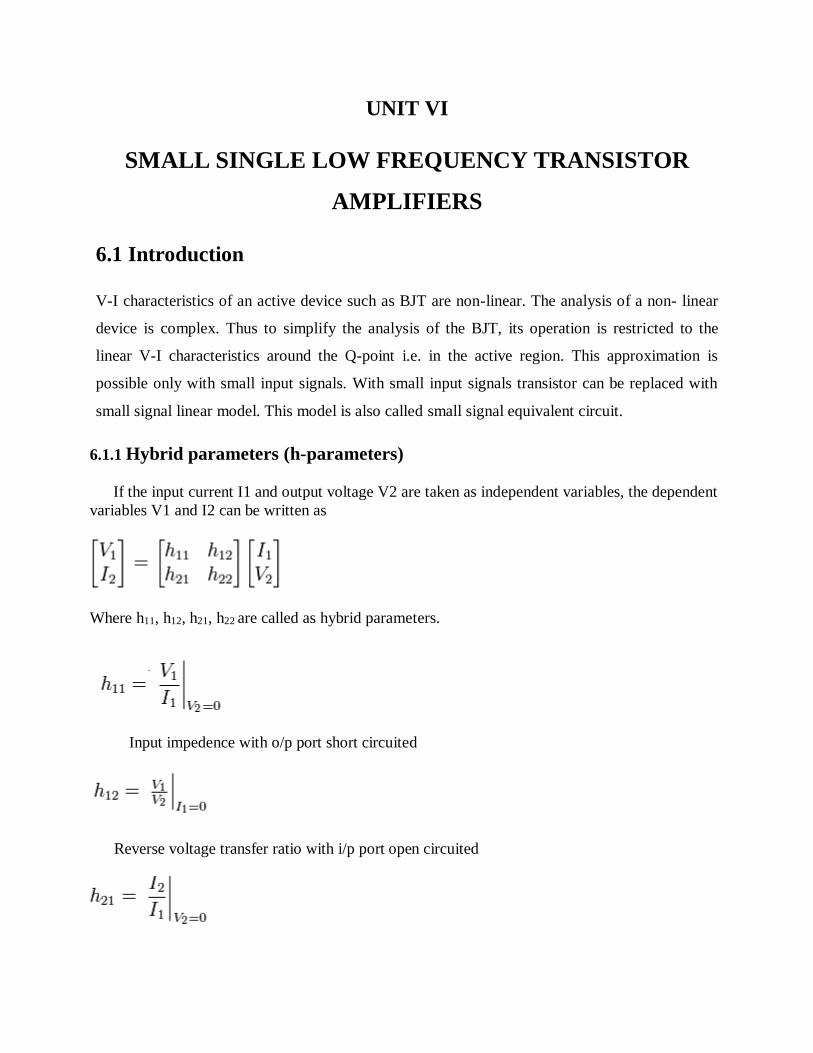
6.1.1 Hybrid parameters (h-parameters)
If the input current I1 and output voltage V2 are taken as independent variables, the dependent
variables V1 and I2 can be written as
Where h11, h12, h21, h22 are called as hybrid parameters.
Input impedence with o/p port short circuited
Reverse voltage transfer ratio with i/p port open circuited
Page 2
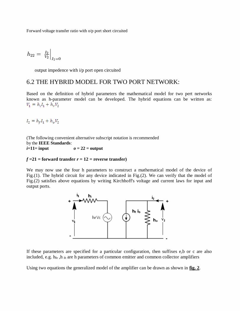
Forward voltage transfer ratio with o/p port short circuited
output impedence with i/p port open circuited
6.2 THE HYBRID MODEL FOR TWO PORT NETWORK:
Based on the definition of hybrid parameters the mathematical model for two pert networks
known as h-parameter model can be developed. The hybrid equations can be written as:
(The following convenient alternative subscript notation is recommended
by the IEEE Standards:
i=11= input o = 22 = output
f =21 = forward transfer r = 12 = reverse transfer)
We may now use the four h parameters to construct a mathematical model of the device of
Fig.(1). The hybrid circuit for any device indicated in Fig.(2). We can verify that the model of
Fig.(2) satisfies above equations by writing Kirchhoff's voltage and current laws for input and
output ports.
If these parameters are specified for a particular configuration, then suffixes e,b or c are also
included, e.g. hfe ,h ib are h parameters of common emitter and common collector amplifiers
Using two equations the generalized model of the amplifier can be drawn as shown in fig. 2.
Page 3
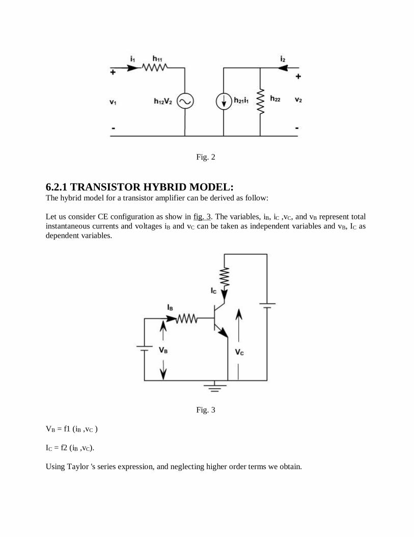
Fig. 2
6.2.1 TRANSISTOR HYBRID MODEL: The hybrid model for a transistor amplifier can be derived as follow:
Let us consider CE configuration as show in fig. 3. The variables, iB, iC ,vC, and vB represent total
instantaneous currents and voltages iB and vC can be taken as independent variables and vB, IC as
dependent variables.
Fig. 3
VB = f1 (iB ,vC )
IC = f2 (iB ,vC).
Using Taylor 's series expression, and neglecting higher order terms we obtain.
Page 4
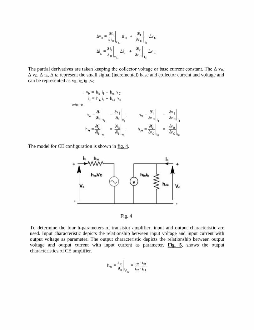
The partial derivatives are taken keeping the collector voltage or base current constant. The Δ vB,
Δ vC, Δ iB, Δ iC represent the small signal (incremental) base and collector current and voltage and
can be represented as vB, iC, iB ,vC
The model for CE configuration is shown in fig. 4.
Fig. 4
To determine the four h-parameters of transistor amplifier, input and output characteristic are
used. Input characteristic depicts the relationship between input voltage and input current with
output voltage as parameter. The output characteristic depicts the relationship between output
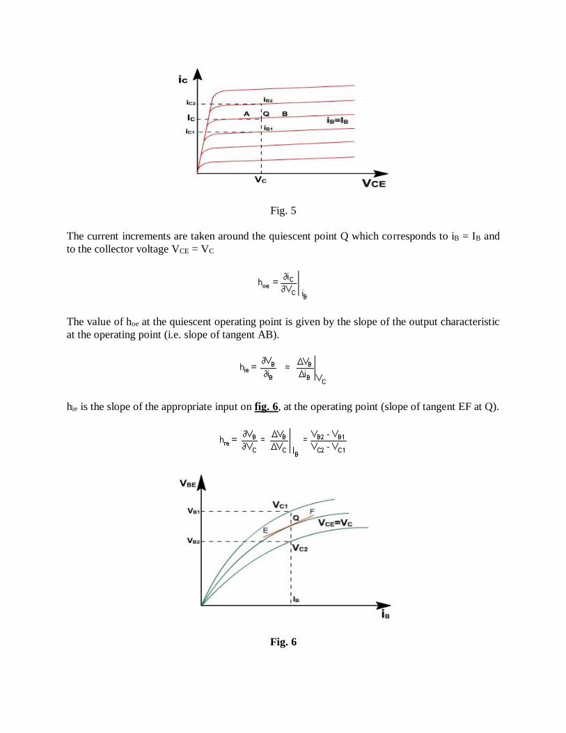
voltage and output current with input current as parameter. Fig. 5, shows the output
characteristics of CE amplifier.
Page 5
Fig. 5
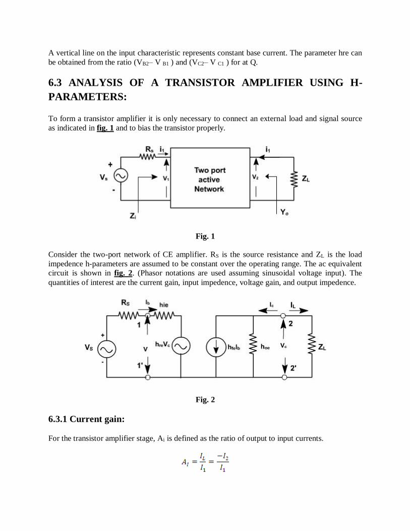
The current increments are taken around the quiescent point Q which corresponds to iB = IB and
to the collector voltage VCE = VC
The value of hoe at the quiescent operating point is given by the slope of the output characteristic
at the operating point (i.e. slope of tangent AB).
hie is the slope of the appropriate input on fig. 6, at the operating point (slope of tangent EF at Q).
Fig. 6
Page 6
A vertical line on the input characteristic represents constant base current. The parameter hre can
be obtained from the ratio (VB2– V B1 ) and (VC2– V C1 ) for at Q.
6.3 ANALYSIS OF A TRANSISTOR AMPLIFIER USING H-
PARAMETERS:
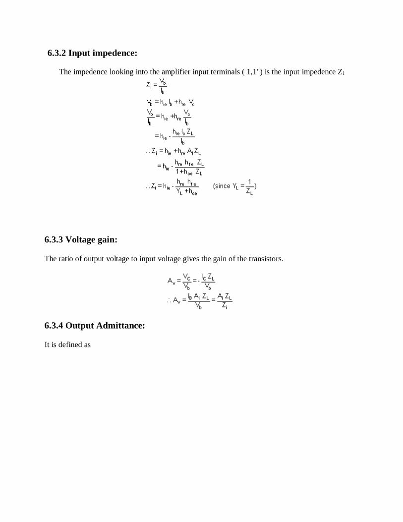
To form a transistor amplifier it is only necessary to connect an external load and signal source
as indicated in fig. 1 and to bias the transistor properly.
Fig. 1
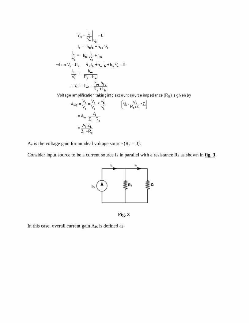
Consider the two-port network of CE amplifier. RS is the source resistance and ZL is the load
impedence h-parameters are assumed to be constant over the operating range. The ac equivalent
circuit is shown in fig. 2. (Phasor notations are used assuming sinusoidal voltage input). The
quantities of interest are the current gain, input impedence, voltage gain, and output impedence.
Fig. 2
6.3.1 Current gain:
For the transistor amplifier stage, Ai is defined as the ratio of output to input currents.
Page 7
6.3.2 Input impedence:
The impedence looking into the amplifier input terminals ( 1,1' ) is the input impedence Z i
6.3.3 Voltage gain:
The ratio of output voltage to input voltage gives the gain of the transistors.
6.3.4 Output Admittance:
It is defined as
Page 8
Av is the voltage gain for an ideal voltage source (Rv = 0).
Consider input source to be a current source IS in parallel with a resistance RS as shown in fig. 3.
Fig. 3
In this case, overall current gain AIS is defined as
Page 9
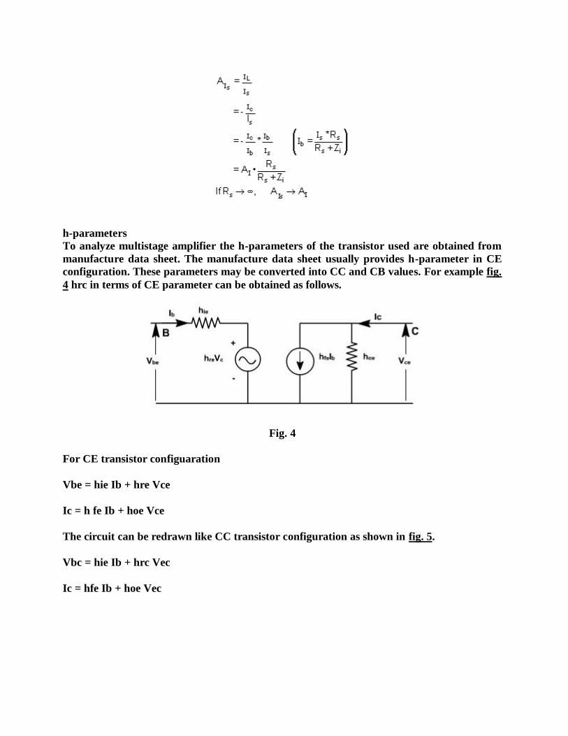
h-parameters
To analyze multistage amplifier the h-parameters of the transistor used are obtained from
manufacture data sheet. The manufacture data sheet usually provides h-parameter in CE
configuration. These parameters may be converted into CC and CB values. For example fig.
4 hrc in terms of CE parameter can be obtained as follows.
Fig. 4
For CE transistor configuaration
Vbe = hie Ib + hre Vce
Ic = h fe Ib + hoe Vce
The circuit can be redrawn like CC transistor configuration as shown in fig. 5.
Vbc = hie Ib + hrc Vec
Ic = hfe Ib + hoe Vec
Page 10
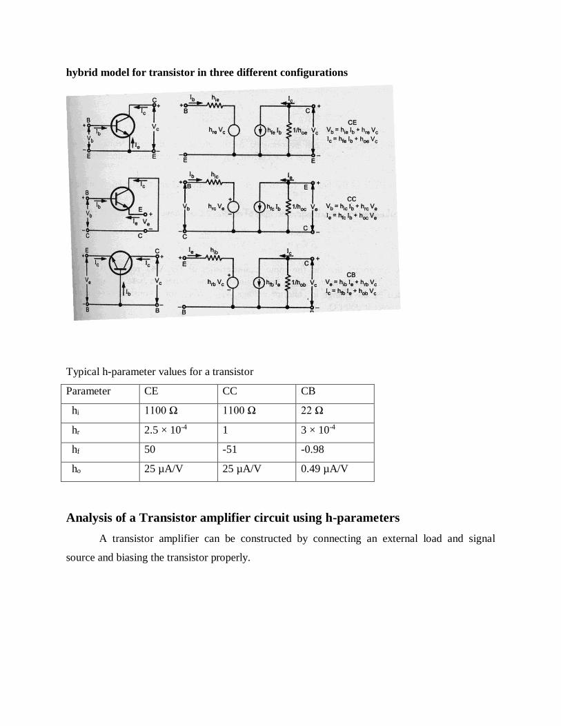
hybrid model for transistor in three different configurations
Typical h-parameter values for a transistor
Parameter CE CC CB
hi 1100 Ω 1100 Ω 22 Ω
hr 2.5 × 10⁻⁴ 1 3 × 10⁻⁴
hf 50 -51 -0.98
ho 25 µA/V 25 µA/V 0.49 µA/V
Analysis of a Transistor amplifier circuit using h-parameters
A transistor amplifier can be constructed by connecting an external load and signal
source and biasing the transistor properly.
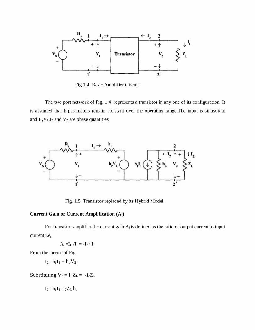
Page 11
Fig.1.4 Basic Amplifier Circuit
The two port network of Fig. 1.4 represents a transistor in any one of its configuration. It
is assumed that h-parameters remain constant over the operating range.The input is sinusoidal
and I1,V1,I2 and V2 are phase quantities
Fig. 1.5 Transistor replaced by its Hybrid Model
Current Gain or Current Amplification (Ai)
For transistor amplifier the current gain Ai is defined as the ratio of output current to input
current,i.e,
Ai =IL /I1 = -I2 / I1
From the circuit of Fig
I2= hf I1 + hoV2
Substituting V2 = ILZL = -I2ZL
I2= hf I1- I2ZL ho
Page 12
I2 + I2ZL ho = hf I1
I2( 1+ ZL ho) = hf I1
Ai = -I2 / I1 = - hf / ( 1+ ZL ho)
Therefore,
Ai = - hf / ( 1+ ZL ho)
Input Impedence (Zi)
In the circuit of Fig , RS is the signal source resistance .The impedence seen when looking into
the amplifier terminals (1,1’) is the amplifier input impedence Zi,
Zi = V1 / I1
From the input circuit of Fig V1 = hi I1 + hrV2
Zi = ( hi I1 + hrV2) / I1
= hi + hr V2 / I1
Substituting
V2 = -I2 ZL = A1I1ZL
Zi = hi + hr A1I1ZL / I1
= hi + hr A1ZL
Substituting for Ai
Zi = hi - hf hr ZL / (1+ hoZL)
= hi - hf hr ZL / ZL(1/ZL+ ho)
Taking the Load admittance as YL =1/ ZL
Zi = hi - hf hr / (YL + ho)
Page 13
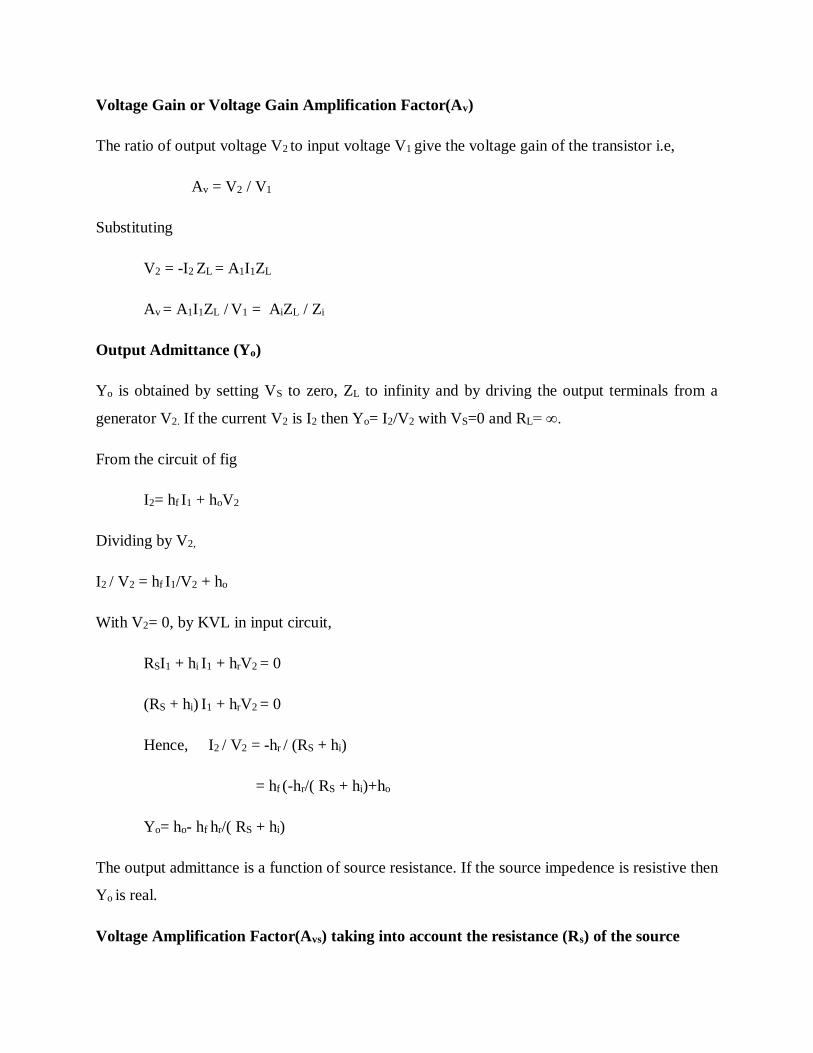
Voltage Gain or Voltage Gain Amplification Factor(Av)
The ratio of output voltage V2 to input voltage V1 give the voltage gain of the transistor i.e,
Av = V2 / V1
Substituting
V2 = -I2 ZL = A1I1ZL
Av = A1I1ZL / V1 = AiZL / Zi
Output Admittance (Yo)
Yo is obtained by setting VS to zero, ZL to infinity and by driving the output terminals from a
generator V2. If the current V2 is I2 then Yo= I2/V2 with VS=0 and RL= ∞.
From the circuit of fig
I2= hf I1 + hoV2
Dividing by V2,
I2 / V2 = hf I1/V2 + ho
With V2= 0, by KVL in input circuit,
RSI1 + hi I1 + hrV2 = 0
(RS + hi) I1 + hrV2 = 0
Hence, I2 / V2 = -hr / (RS + hi)
= hf (-hr/( RS + hi)+ho
Yo= ho- hf hr/( RS + hi)
The output admittance is a function of source resistance. If the source impedence is resistive then
Yo is real.
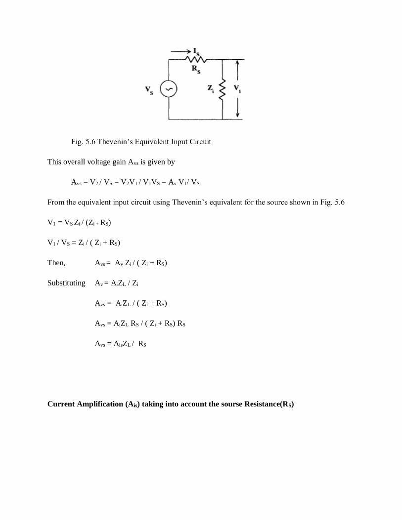
Voltage Amplification Factor(Avs) taking into account the resistance (Rs) of the source
Page 14
Fig. 5.6 Thevenin’s Equivalent Input Circuit
This overall voltage gain Avs is given by
Avs = V2 / VS = V2V1 / V1VS = Av V1/ VS
From the equivalent input circuit using Thevenin’s equivalent for the source shown in Fig. 5.6
V1 = VS Zi / (Zi + RS)
V1 / VS = Zi / ( Zi + RS)
Then, Avs = Av Zi / ( Zi + RS)
Substituting Av = AiZL / Zi
Avs = AiZL / ( Zi + RS)
Avs = AiZL RS / ( Zi + RS) RS
Avs = AisZL / RS
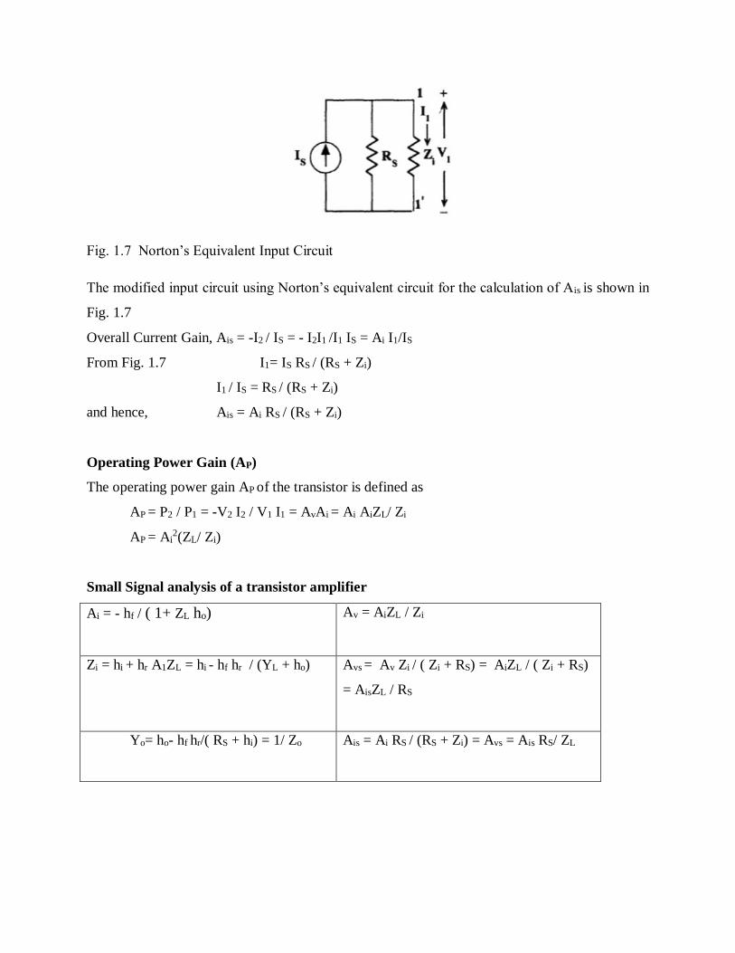
Current Amplification (Ais) taking into account the sourse Resistance(RS)
Page 15
Fig. 1.7 Norton’s Equivalent Input Circuit
The modified input circuit using Norton’s equivalent circuit for the calculation of Ais is shown in
Fig. 1.7
Overall Current Gain, Ais = -I2 / IS = - I2I1 /I1 IS = Ai I1/IS
From Fig. 1.7 I1= IS RS / (RS + Zi)
I1 / IS = RS / (RS + Zi)
and hence, Ais = Ai RS / (RS + Zi)
Operating Power Gain (AP)
The operating power gain AP of the transistor is defined as
AP = P2 / P1 = -V2 I2 / V1 I1 = AvAi = Ai AiZL/ Zi
AP = Ai2(ZL/ Zi)
Small Signal analysis of a transistor amplifier
Ai = - hf / ( 1+ ZL ho)
Av = AiZL / Zi
Zi = hi + hr A1ZL = hi - hf hr / (YL + ho)
Avs = Av Zi / ( Zi + RS) = AiZL / ( Zi + RS)
= AisZL / RS
Yo= ho- hf hr/( RS + hi) = 1/ Zo
Ais = Ai RS / (RS + Zi) = Avs = Ais RS/ ZL
Page 16
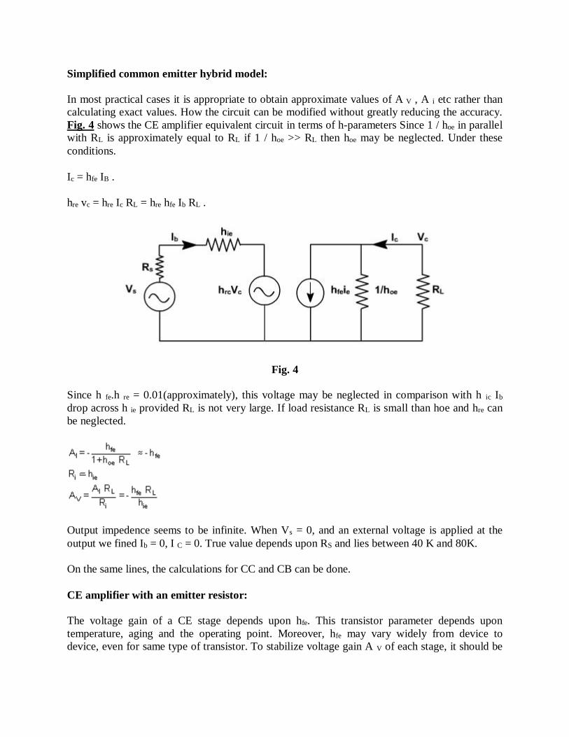
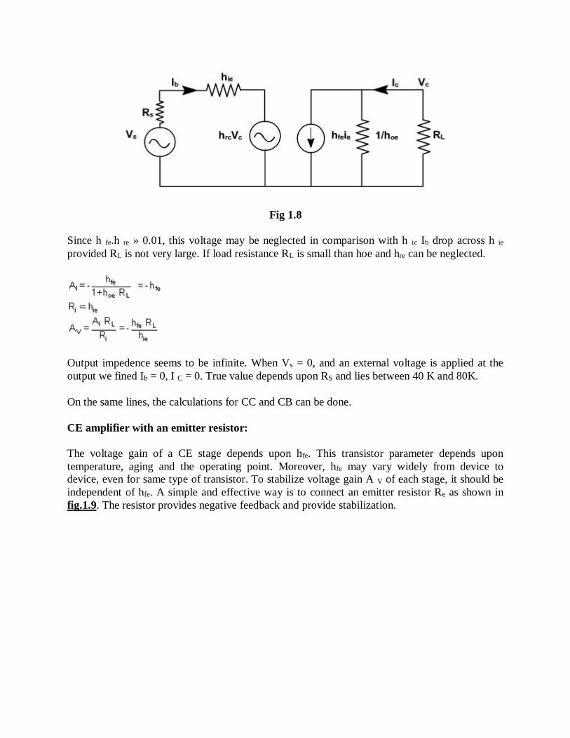
Simplified common emitter hybrid model:
In most practical cases it is appropriate to obtain approximate values of A V , A i etc rather than
calculating exact values. How the circuit can be modified without greatly reducing the accuracy.
Fig. 4 shows the CE amplifier equivalent circuit in terms of h-parameters Since 1 / hoe in parallel
with RL is approximately equal to RL if 1 / hoe >> RL then hoe may be neglected. Under these
conditions.
Ic = hfe IB .
hre vc = hre Ic RL = hre hfe Ib RL .
Fig. 4
Since h fe.h re = 0.01(approximately), this voltage may be neglected in comparison with h ic Ib
drop across h ie provided RL is not very large. If load resistance RL is small than hoe and hre can
be neglected.
Output impedence seems to be infinite. When Vs = 0, and an external voltage is applied at the
output we fined Ib = 0, I C = 0. True value depends upon RS and lies between 40 K and 80K.
On the same lines, the calculations for CC and CB can be done.
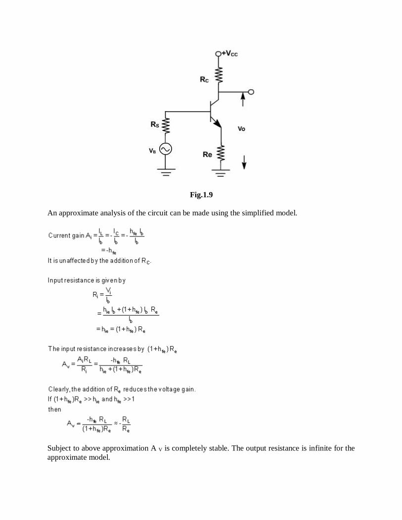
CE amplifier with an emitter resistor:
The voltage gain of a CE stage depends upon hfe. This transistor parameter depends upon
temperature, aging and the operating point. Moreover, hfe may vary widely from device to
device, even for same type of transistor. To stabilize voltage gain A V of each stage, it should be
Page 17
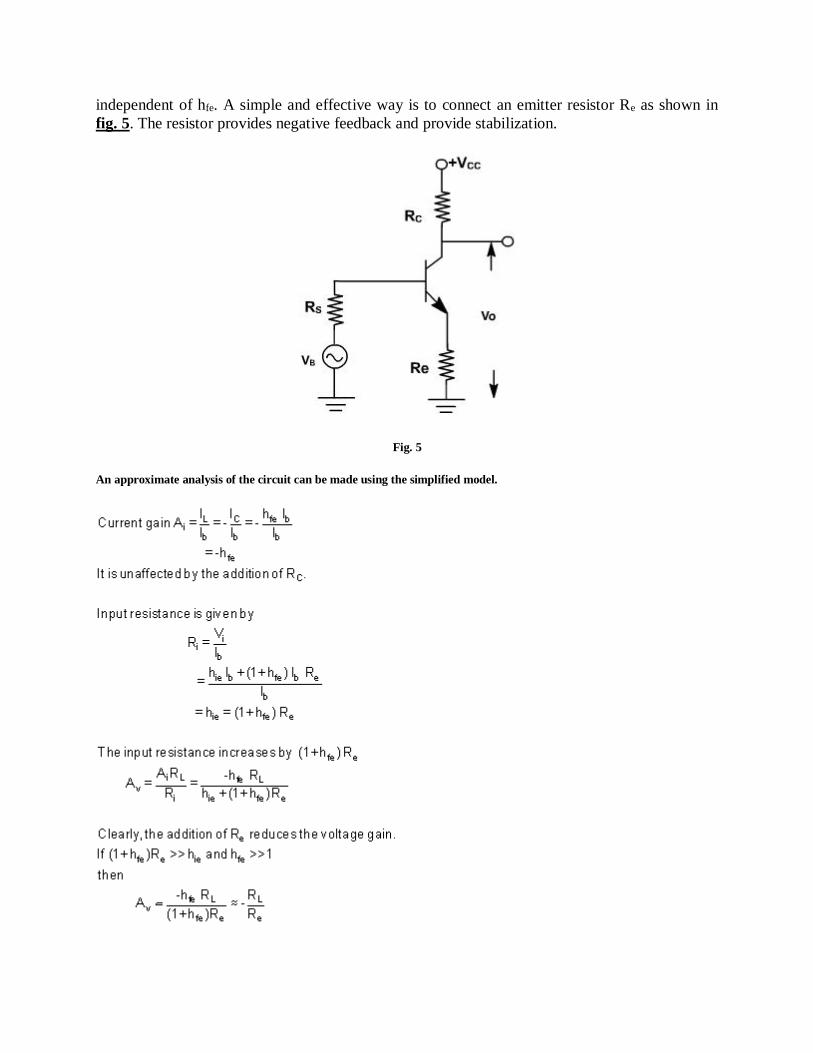
independent of hfe. A simple and effective way is to connect an emitter resistor Re as shown in
fig. 5. The resistor provides negative feedback and provide stabilization.
Fig. 5
An approximate analysis of the circuit can be made using the simplified model.
Page 18
Subject to above approximation A V is completely stable. The output resistance is infinite for the approximate model.
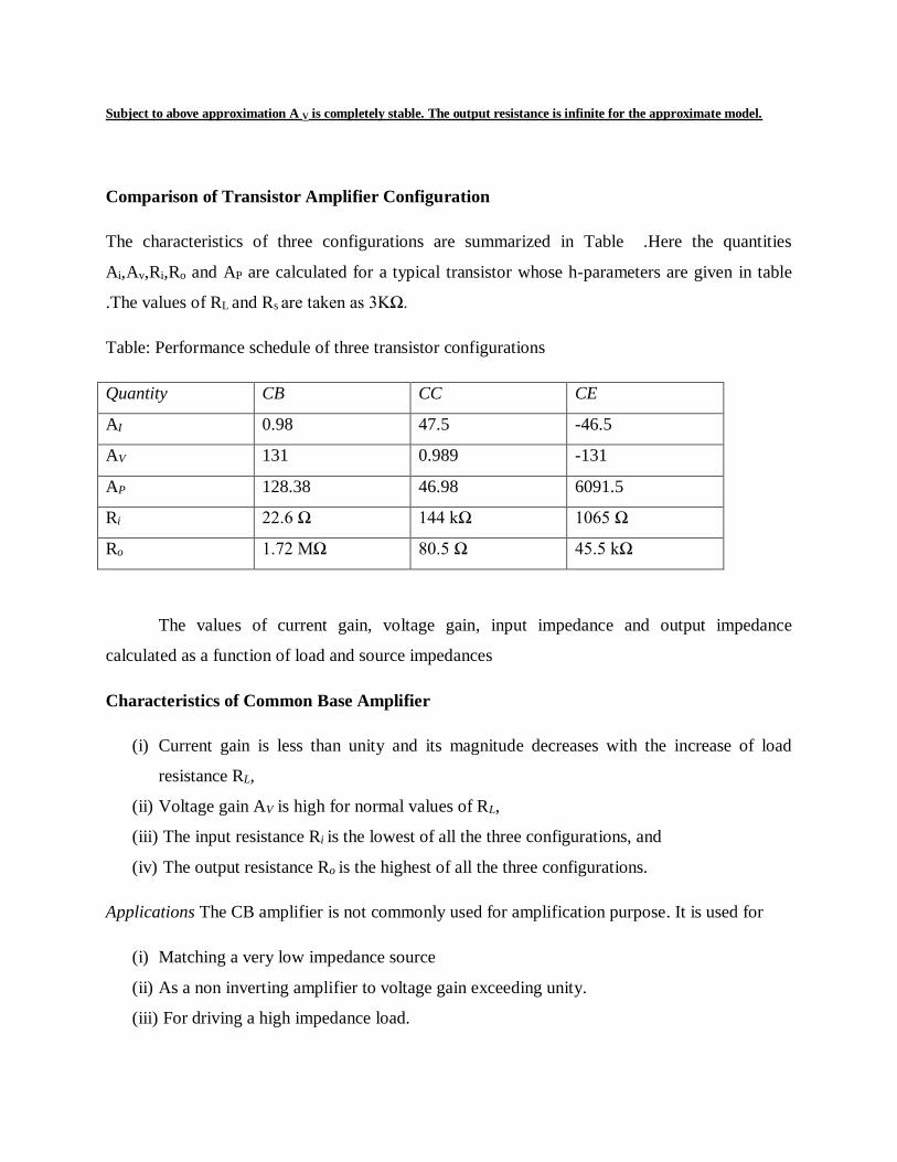
Comparison of Transistor Amplifier Configuration
The characteristics of three configurations are summarized in Table .Here the quantities
Ai,Av,Ri,Ro and AP are calculated for a typical transistor whose h-parameters are given in table
.The values of RL and Rs are taken as 3KΩ.
Table: Performance schedule of three transistor configurations
Quantity CB CC CE
AI 0.98 47.5 -46.5
AV 131 0.989 -131
AP 128.38 46.98 6091.5
Ri 22.6 Ω 144 kΩ 1065 Ω
Ro 1.72 MΩ 80.5 Ω 45.5 kΩ
The values of current gain, voltage gain, input impedance and output impedance
calculated as a function of load and source impedances
Characteristics of Common Base Amplifier
(i) Current gain is less than unity and its magnitude decreases with the increase of load
resistance RL,
(ii) Voltage gain AV is high for normal values of RL,
(iii) The input resistance Ri is the lowest of all the three configurations, and
(iv) The output resistance Ro is the highest of all the three configurations.
Applications The CB amplifier is not commonly used for amplification purpose. It is used for
(i) Matching a very low impedance source
(ii) As a non inverting amplifier to voltage gain exceeding unity.
(iii) For driving a high impedance load.
Page 19
(iv) As a constant current source.
Characteristics of Common Collector Amplifier
(i) For low RL (< 10 kΩ), the current gain Ai is high and almost equal to that of a CE
amplifier.
(ii) The voltage gain AV is less than unity.
(iii) The input resistance is the highest of all the three configurations.
(iv) The output resistance is the lowest of all the three configurations.
Applications The CC amplifier is widely used as a buffer stage between a high impedance source
and a low impedance load.
Characteristics of Common Emitter Amplifier
(i) The current gain Ai is high for RL < 10 kΩ.
(ii) The voltage gain is high for normal values of load resistance RL.
(iii) The input resistance Ri is medium.
(iv) The output resistance Ro is moderately high.
Applications: CE amplifier is widely used for amplification.
Simplified common emitter hybrid model:
In most practical cases it is appropriate to obtain approximate values of A V , A i etc rather than
calculating exact values. How the circuit can be modified without greatly reducing the accuracy.
Fig 1. 8 shows the CE amplifier equivalent circuit in terms of h-parameters Since 1 / hoe in
parallel with RL is approximately equal to RL if 1 / hoe >> RL then hoe may be neglected. Under
these conditions.
Ic = hfe IB .
hre vc = hre Ic RL = hre hfe Ib RL .
Page 20
Fig 1.8
Since h fe.h re » 0.01, this voltage may be neglected in comparison with h ic Ib drop across h ie
provided RL is not very large. If load resistance RL is small than hoe and hre can be neglected.
Output impedence seems to be infinite. When Vs = 0, and an external voltage is applied at the
output we fined Ib = 0, I C = 0. True value depends upon RS and lies between 40 K and 80K.
On the same lines, the calculations for CC and CB can be done.
CE amplifier with an emitter resistor:
The voltage gain of a CE stage depends upon hfe. This transistor parameter depends upon
temperature, aging and the operating point. Moreover, hfe may vary widely from device to
device, even for same type of transistor. To stabilize voltage gain A V of each stage, it should be
independent of hfe. A simple and effective way is to connect an emitter resistor Re as shown in
fig.1.9. The resistor provides negative feedback and provide stabilization.
Page 21
Fig.1.9
An approximate analysis of the circuit can be made using the simplified model.
Subject to above approximation A V is completely stable. The output resistance is infinite for the
approximate model.
Page 22
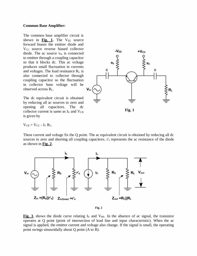
Common Base Amplifier:
The common base amplifier circuit is
shown in Fig. 1. The VEE source
forward biases the emitter diode and
VCC source reverse biased collector
diode. The ac source vin is connected
to emitter through a coupling capacitor
so that it blocks dc. This ac voltage
produces small fluctuation in currents
and voltages. The load resistance RL is
also connected to collector through
coupling capacitor so the fluctuation
in collector base voltage will be
observed across RL.
The dc equivalent circuit is obtained
by reducing all ac sources to zero and
opening all capacitors. The dc
collector current is same as IE and VCB
is given by
VCB = VCC - IC RC.
Fig. 1
These current and voltage fix the Q point. The ac equivalent circuit is obtained by reducing all dc
sources to zero and shorting all coupling capacitors. r'e represents the ac resistance of the diode
as shown in Fig. 2.
Fig. 2
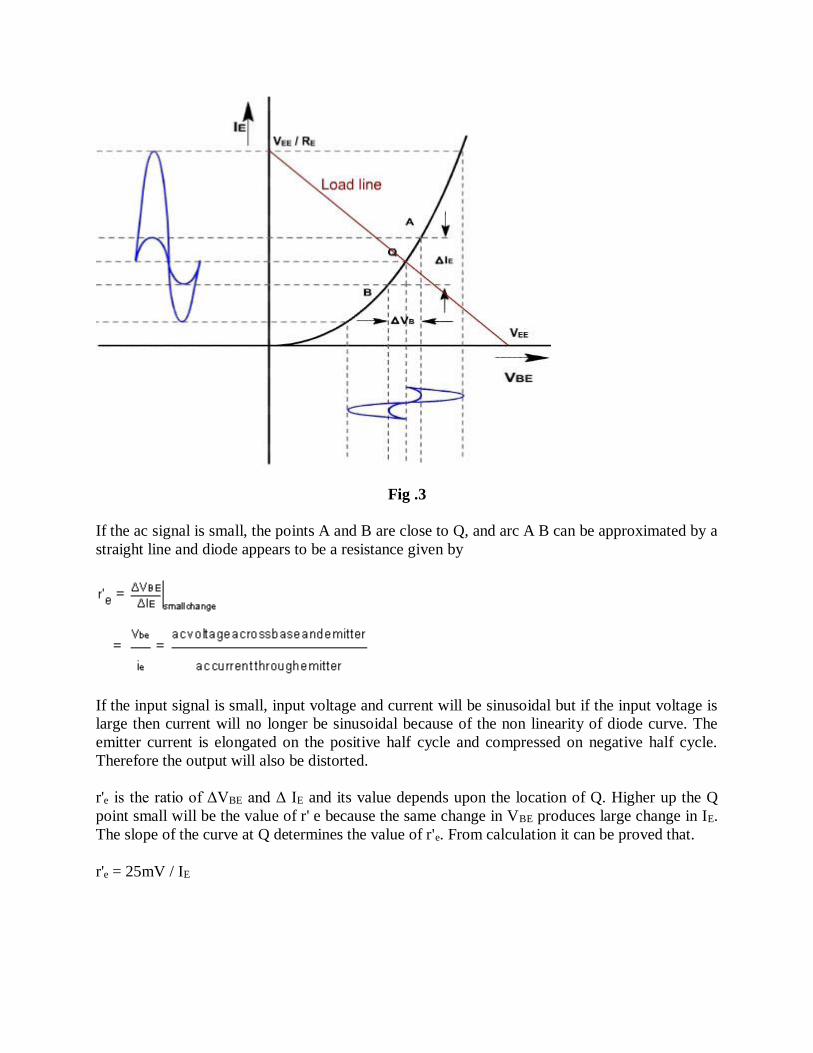
Fig. 3, shows the diode curve relating IE and VBE. In the absence of ac signal, the transistor
operates at Q point (point of intersection of load line and input characteristic). When the ac
signal is applied, the emitter current and voltage also change. If the signal is small, the operating
point swings sinusoidally about Q point (A to B).
Page 23
Fig .3
If the ac signal is small, the points A and B are close to Q, and arc A B can be approximated by a
straight line and diode appears to be a resistance given by
If the input signal is small, input voltage and current will be sinusoidal but if the input voltage is
large then current will no longer be sinusoidal because of the non linearity of diode curve. The
emitter current is elongated on the positive half cycle and compressed on negative half cycle.
Therefore the output will also be distorted.
r'e is the ratio of ΔVBE and Δ IE and its value depends upon the location of Q. Higher up the Q
point small will be the value of r' e because the same change in VBE produces large change in IE.
The slope of the curve at Q determines the value of r'e. From calculation it can be proved that.
r'e = 25mV / IE
Page 24
Common Base Amplifier
Proof:
In general, the current through a diode is given by
Where q is he charge on electron, V is the drop across diode, T is the temperature and K is a
constant.
On differentiating w.r.t V, we get,
The value of (q / KT) at 25°C is approximately 40.
Therefore,
or,
To a close approximation the small changes in collector current equal the small changes in
emitter current. In the ac equivalent circuit, the current ‘iC' is shown upward because if ‘ie'
increases, then ‘iC' also increases in the same direction.
Voltage gain:
Since the ac input voltage source is connected across r'e. Therefore, the ac emitter current is
given by
ie = Vin / r'e
or, Vin = ie r'e
The output voltage is given by Vout = ic (RC || RL)
Page 25
Under open circuit condition vout = ic Rc
Small Signal CE Amplifiers:
CE amplifiers are very popular to amplify the small signal ac. After a transistor has been biased
with a Q point near the middle of a dc load line, ac source can be coupled to the base. This
produces fluctuations in the base current and hence in the collector current of the same shape and
frequency. The output will be enlarged sine wave of same frequency.
The amplifier is called linear if it does not change the wave shape of the signal. As long as the
input signal is small, the transistor will use only a small part of the load line and the operation
will be linear.
On the other hand, if the input signal is too large. The fluctuations along the load line will drive
the transistor into either saturation or cut off. This clips the peaks of the input and the amplifier is
no longer linear.
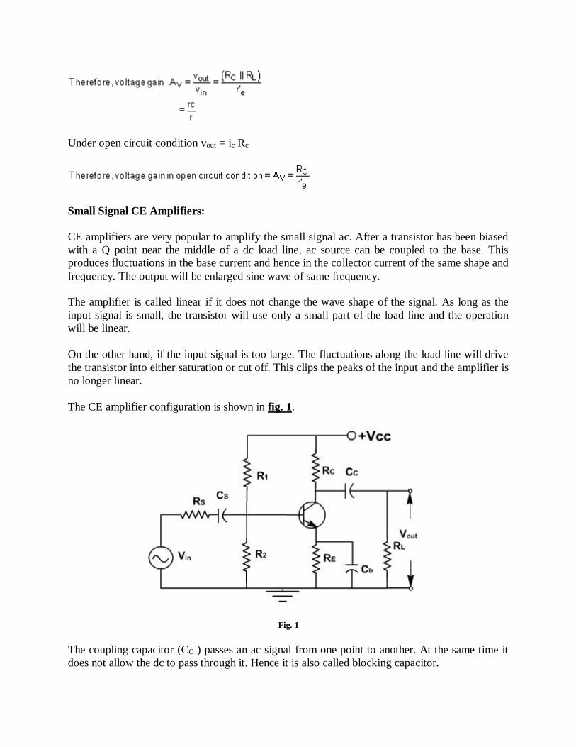
The CE amplifier configuration is shown in fig. 1.
Fig. 1
The coupling capacitor (CC ) passes an ac signal from one point to another. At the same time it
does not allow the dc to pass through it. Hence it is also called blocking capacitor.
Page 26
Fig. 2
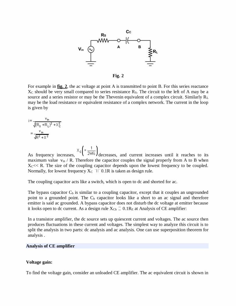
For example in fig. 2, the ac voltage at point A is transmitted to point B. For this series reactance
XC should be very small compared to series resistance RS. The circuit to the left of A may be a
source and a series resistor or may be the Thevenin equivalent of a complex circuit. Similarly RL
may be the load resistance or equivalent resistance of a complex network. The current in the loop
is given by
As frequency increases, decreases, and current increases until it reaches to its
maximum value vin / R. Therefore the capacitor couples the signal properly from A to B when
XC<< R. The size of the coupling capacitor depends upon the lowest frequency to be coupled.
Normally, for lowest frequency XC 0.1R is taken as design rule.
The coupling capacitor acts like a switch, which is open to dc and shorted for ac.
The bypass capacitor Cb is similar to a coupling capacitor, except that it couples an ungrounded
point to a grounded point. The Cb capacitor looks like a short to an ac signal and therefore
emitter is said ac grounded. A bypass capacitor does not disturb the dc voltage at emitter because
it looks open to dc current. As a design rule XCb 0.1RE at Analysis of CE amplifier:
In a transistor amplifier, the dc source sets up quiescent current and voltages. The ac source then
produces fluctuations in these current and voltages. The simplest way to analyze this circuit is to
split the analysis in two parts: dc analysis and ac analysis. One can use superposition theorem for
analysis .
Analysis of CE amplifier
Voltage gain:
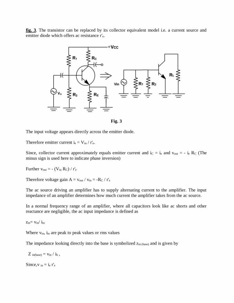
To find the voltage gain, consider an unloaded CE amplifier. The ac equivalent circuit is shown in
Page 27
fig. 3. The transistor can be replaced by its collector equivalent model i.e. a current source and
emitter diode which offers ac resistance r'e.
Fig. 3
The input voltage appears directly across the emitter diode.
Therefore emitter current ie = Vin / r'e.
Since, collector current approximately equals emitter current and iC = ie and vout = - ie RC (The
minus sign is used here to indicate phase inversion)
Further vout = - (Vin RC) / r'e
Therefore voltage gain A = vout / vin = -RC / r'e
The ac source driving an amplifier has to supply alternating current to the amplifier. The input
impedance of an amplifier determines how much current the amplifier takes from the ac source.
In a normal frequency range of an amplifier, where all capacitors look like ac shorts and other
reactance are negligible, the ac input impedance is defined as
zin= vin/ iin
Where vin, iin are peak to peak values or rms values
The impedance looking directly into the base is symbolized zin (base) and is given by
Z in(base) = vin / ib ,
Since,v in = ie r'e
Page 28
zin (base) = r'e.
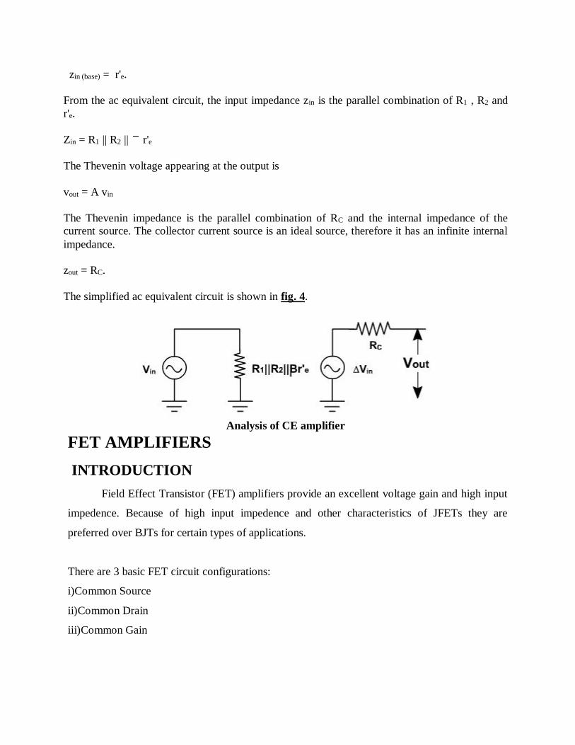
From the ac equivalent circuit, the input impedance zin is the parallel combination of R1 , R2 and
r'e.
Zin = R1 || R2 || r'e
The Thevenin voltage appearing at the output is
vout = A vin
The Thevenin impedance is the parallel combination of RC and the internal impedance of the
current source. The collector current source is an ideal source, therefore it has an infinite internal
impedance.
zout = RC.
The simplified ac equivalent circuit is shown in fig. 4.
Analysis of CE amplifier
FET AMPLIFIERS
INTRODUCTION
Field Effect Transistor (FET) amplifiers provide an excellent voltage gain and high input
impedence. Because of high input impedence and other characteristics of JFETs they are
preferred over BJTs for certain types of applications.
There are 3 basic FET circuit configurations:
i)Common Source
ii)Common Drain
iii)Common Gain
Page 29
Similar to BJT CE,CC and CB circuits, only difference is in BJT large output collector
current is controlled by small input base current whereas FET controls output current by means
of small input voltage. In both the cases output current is controlled variable.
FET amplifier circuits use voltage controlled nature of the JFET. In Pinch off region, ID
depends only on VGS.
THE FET SMALL SIGNAL MODEL:-
The linear small signal equivalent circuit for the FET can be obtained in a manner similar to that
used to derive the corresponding model for a transistor.
We can express the drain current iD as a function f of the gate voltage and drain voltage Vds.
Id =f(Vgs,Vds)------------------(1)
The transconductance gm and drain resistance rd:-
If both gate voltage and drain voltage are varied, the change in the drain current is approximated
by using taylors series considering only the first two terms in the expansion
∆id= |vds=constant .∆vgs |vgs=constant∆vds
we can write ∆id=id
∆vgs=vgs
∆vds=vds
Id=gm v Vds→(1)
Where gm= |Vds |Vds
gm= |Vds
Is the mutual conductance or transconductance .It is also called as gfs or yfs common source
forward conductance .
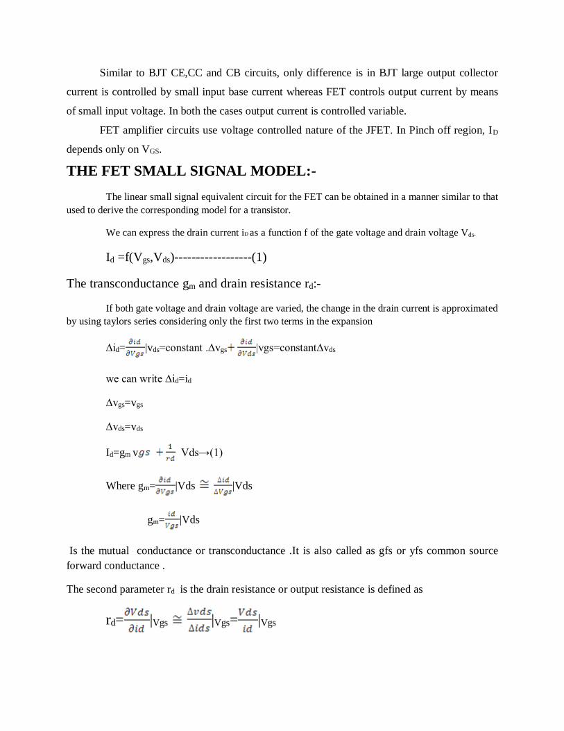
The second parameter rd is the drain resistance or output resistance is defined as
rd= |Vgs |Vgs= |Vgs
Page 30
rd= |Vgs
The reciprocal of the rd is the drain conductance gd .It is also designated by Yos and
Gos and called the common source output conductance . So the small signal equivalent circuit
for FET can be drawn in two different ways.
1.small signal current –source model
2.small signal voltage-source model.
A small signal current –source model for FET in common source configuration can be
drawn satisfying Eq→(1) as shown in the figure(a)
This low frequency model for FET has a Norton’s output circuit with a dependent
current generator whose magnitude is proportional to the gate-to –source voltage. The
proportionality factor is the transconductance ‘gm’. The output resistance is ‘rd’. The input
resistance between the gate and source is infinite, since it is assumed that the reverse biased gate
draws no current. For the same reason the resistance between gate and drain is assumed to be
infinite.
The small signal voltage-source model is shown in the figure(b).
This can be derived by finding the Thevenin’s equivalent for the output part of fig(a) .
These small signal models for FET can be used for analyzing the three basic FET
amplifier configurations:
1.common source (CS) 2.common drain (CD) or source follower
3. common gate(CG).
(a)Small Signal Current source model for FET (b)Small Signal voltage source model for FET
Here the input circuit is kept open because of having high input impedance and the output
circuit satisfies the equation for ID
Page 31
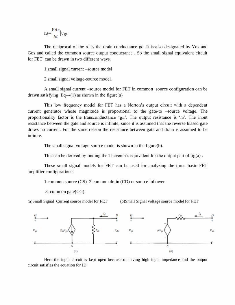
Common Source (CS) Amplifier
Fig. 7.1 (a) CS Amplifier (b) Small-signal equivalent circuit
A simple Common Source amplifier is shown in Fig. 7.1(a) and associated small signal
equivalent circuit using voltage-source model of FET is shown in Fig. 7.1(b)
Voltage Gain
Source resistance (RS) is used to set the Q-Point but is bypassed by CS for mid-frequency
operation. From the small signal equivalent circuit ,the output voltage
VO = -RDµVgs(RD + rd)
Where Vgs = Vi , the input voltage,
Hence, the voltage gain,
AV = VO / Vi = -RDµ(RD + rd)
Input Impedence
From Fig. 7.1(b) Input Impedence is
Zi = RG
For voltage divider bias as in CE Amplifiers of BJT
RG = R1 R2
Page 32
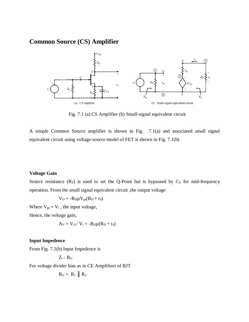
Output Impedance
Output impedance is the impedance measured at the output terminals with the input voltage VI =
0
From the Fig. 7.1(b) when the input voltage Vi = 0, Vgs = 0 and hence
µ Vgs = 0
The equivalent circuit for calculating output impedence is given in Fig. 7.2.
Output impedence Zo = rd RD
Normally rd will be far greater than RD . Hence Zo ≈ RD
Common Drain Amplifier
A simple common drain amplifier is shown in Fig. 7.2(a) and associated small signal equivalent
circuit using the voltage source model of FET is shown in Fig. 7.2(b).Since voltage Vgd is more
easily determined than Vgs, the voltage source in the output circuit is expressed in terms of Vgs
and Thevenin’s theorem.
Fig. 7.2 (a)CD Amplifier (b)Small-signal equivalent circuit
Voltage Gain
The output voltage,
VO = RSµVgd / (µ + 1) RS + rd
Where Vgd = Vi the input voltage.
Hence, the voltage gain,
Av = VO / Vi = RSµ / (µ + 1) RS + rd
Input Impedence
Page 33
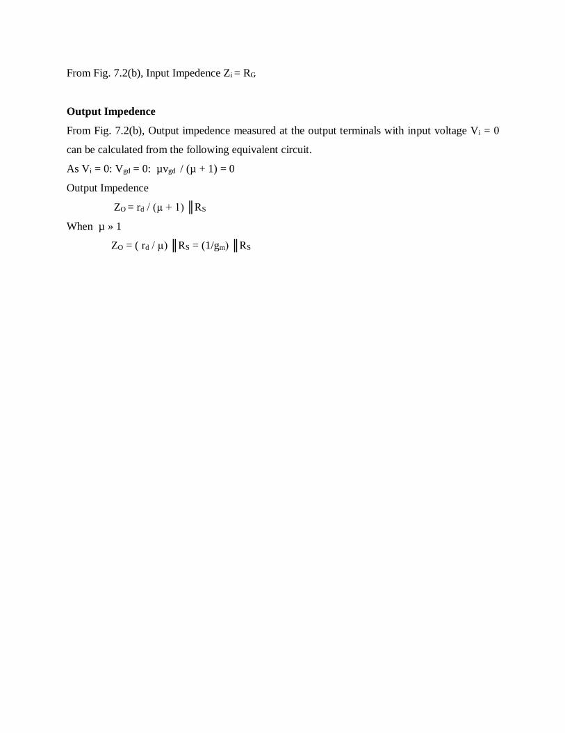
From Fig. 7.2(b), Input Impedence Zi = RG
Output Impedence
From Fig. 7.2(b), Output impedence measured at the output terminals with input voltage Vi = 0
can be calculated from the following equivalent circuit.
As Vi = 0: Vgd = 0: µvgd / (µ + 1) = 0
Output Impedence
ZO = rd / (µ + 1) RS
When µ » 1
ZO = ( rd / µ) RS = (1/gm) RS
![RESEARCHARTICLE ThePerilsofAdaptingtoDoseErrorsin ...vvmisic/chan_misic_perils_of_dose...In [23]wealsodescribe twoothermethodsforupdating δ and δ ,thereactive− methodand thereactive+](https://static.documents.pub/doc/80x56/60c502aa35167d03ba1ef42f/researcharticle-theperilsofadaptingtodoseerrorsin-vvmisicchanmisicperilsofdose.jpg)


![Single-spinasymmetries with 2 hadron fragmentation: The ... · 0.5 0.55 0.6 0.65 0.7 0.75 0.8 0.85 0.9 0.95 1 Mhh [GeV] sin δ 0 sin δ p sin(δ 0-δ p) Fit data with: À Á Â Ã](https://static.documents.pub/doc/80x56/5fc888da40e2897c3b5a2e4f/single-spinasymmetries-with-2-hadron-fragmentation-the-05-055-06-065-07.jpg)


![Introduction to Algorithms · 2019. 9. 13. · Initializing d[s] ←0 and d[v] ←∞for all v ∈V –{s} establishes d[v] ≥δ(s, v) for all v ∈V, and this invariant is maintained](https://static.documents.pub/doc/80x56/60c8e523b1e4b33eb447aec1/introduction-to-algorithms-2019-9-13-initializing-ds-a0-and-dv-aafor.jpg)


