Page 1
Soliton based Return to Zero Logic using 180nm CMOS
Sai Venkatesh Balasubramanian
Sree Sai Vidhya Mandhir, Mallasandra, Bengaluru-560109, Karnataka, India.
[email protected]
Abstract: A Return-to-Zero Logic consisting of Soliton based clock is proposed, and is seen to exhibit more
robustness in propagation through interconnects compared with conventional square pulses at
microwave and millimeter wave frequencies. The generation of solitons using the nonlinearity of a
single transistor is discussed and various combinational and sequential logic circuits based on
soliton logic are implemented and characterized using Deep Submicron VLSI SPICE
implementations at 180nm CMOS Technology. In addition, Pulse Compression based on single
transistor is also discussed. The simplicity of implementation of the soliton logic, coupled with the
compatibility with existing CMOS technologies form the key highlights of the present work, paving
the way for a futuristic low distortion computing era.
Keywords: Soliton, Return to Zero Logic, Microwind, 180nm CMOS, Pulse Compression
1. Introduction: Most state-of-the-art computing systems operating on microwave and millimeter wave frequencies
encounter a common problem - signal distortion1,2,3
. Analysis of the spectral features of the clock signal
used, namely the square wave, clearly indicate the pitfalls in using such a signal, briefly described as
follows: the square wave, theoretically having infinite frequency components, experiences severe high-
frequency attenuation while propagating through transmission channels and interconnects, which have
been shown to exhibit a low pass behavior4. These effects become more pre-dominant at the higher
Gigahertz and Terahertz frequencies, where even interconnects within and between chips significantly
attenuate high frequency components5,6,7
.
The present work attempts to address this problem by proposing a return-to-zero logic system based on
Gaussian-like soliton pulses, building on the successful application of such pulses in photonics
technology8. It is seen that the solitons have lesser dominance of high frequency components unlike the
square wave along with providing good switching characteristics8. Transmission Line models are used to
compare the robustness of the square wave and pulse-based clocks on propagation along typical
microstrip interconnects. A Return-to-zero logic is then proposed using the presence of the pulse as logic
“high” and the absence as logic “low”. The generation of the pulses using the nonlinearity of a single
CMOS inverter is then described and implemented in deep submicron VLSI level SPICE using 180nm
technology. The basic units of combinational and sequential logic - the NAND Gate and the RS NAND
Latch are then implemented and the waveforms are analyzed. Also, a typical combinational circuit - the
2:1 multiplexer and a typical memory element - the 6 terminal Static RAM are described. Finally, a very
important and useful phenomenon in the context of high-speed soliton clocks, namely pulse compression
is explored. The use of extremely simple circuitry to generate the solitons, coupled with the observed
robustness of solitons in comparison with conventional square based clock signals form the main
highlights of the present work.
Page 2
2. The Concept of Solitons The concept of using Solitons as carriers in low-distortion communication systems has its origin in optical
communications, where the „soliton‟ is defined as a solution to the Nonlinear Schrödinger Equation
(NLSE) depicting pulse propagation in optical fibers8. The NLSE and its hyperbolic secant based solution
are a mathematical characterization of the exact balance between the dispersive and nonlinear effects of
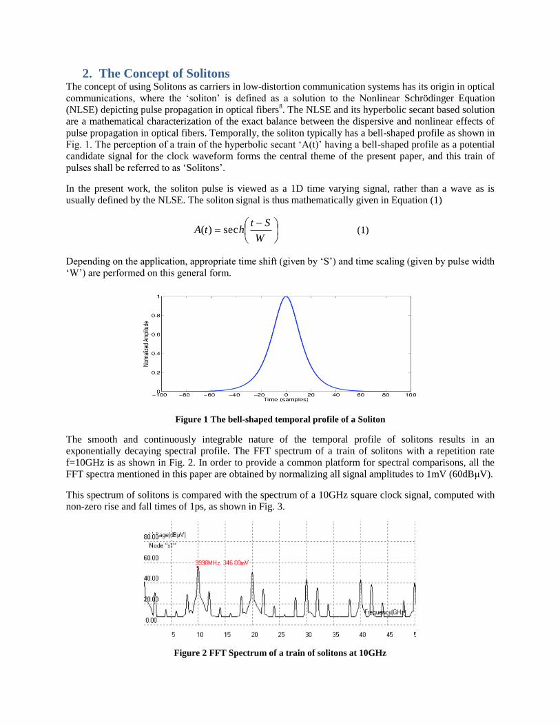
pulse propagation in optical fibers. Temporally, the soliton typically has a bell-shaped profile as shown in
Fig. 1. The perception of a train of the hyperbolic secant „A(t)‟ having a bell-shaped profile as a potential
candidate signal for the clock waveform forms the central theme of the present paper, and this train of
pulses shall be referred to as „Solitons‟.
In the present work, the soliton pulse is viewed as a 1D time varying signal, rather than a wave as is
usually defined by the NLSE. The soliton signal is thus mathematically given in Equation (1)
W
SthtA sec)( (1)
Depending on the application, appropriate time shift (given by „S‟) and time scaling (given by pulse width
„W‟) are performed on this general form.
Figure 1 The bell-shaped temporal profile of a Soliton
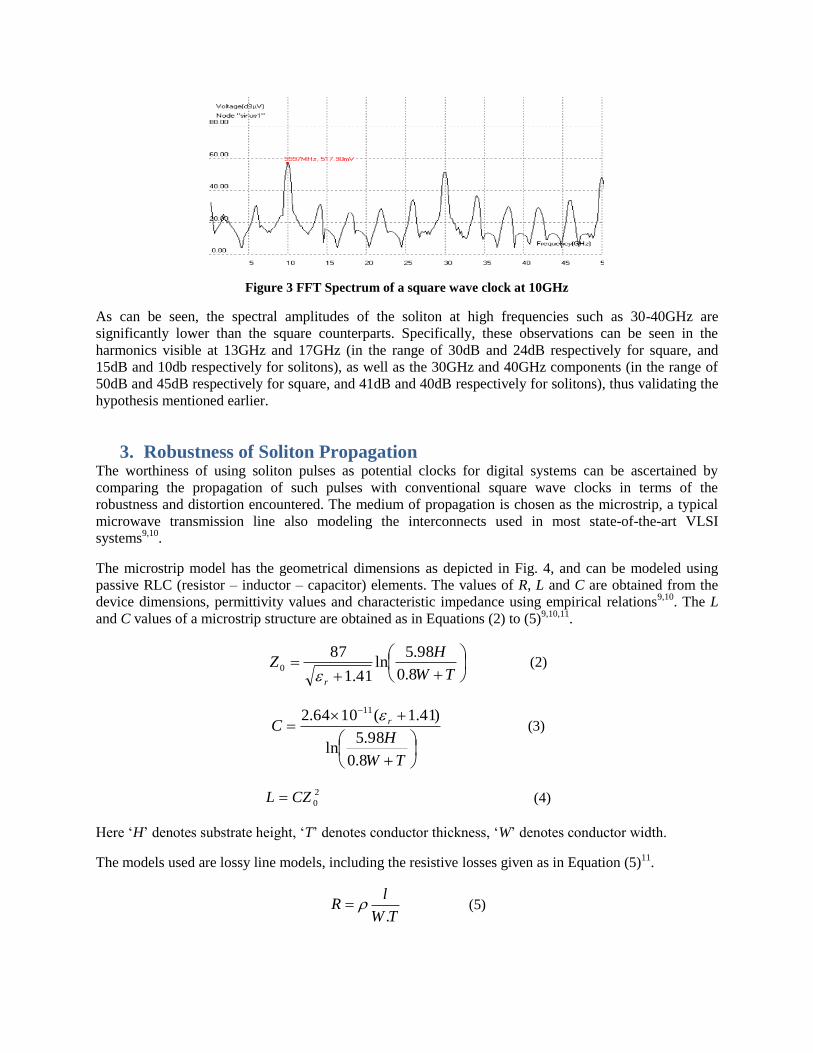
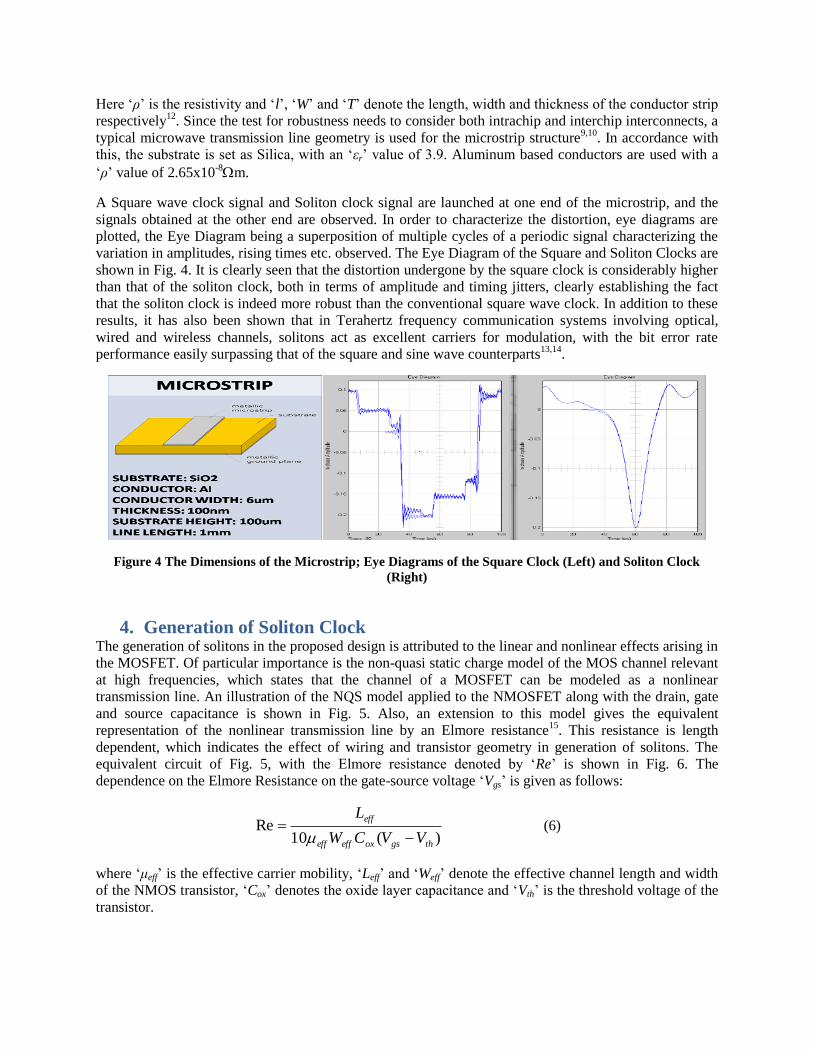
The smooth and continuously integrable nature of the temporal profile of solitons results in an
exponentially decaying spectral profile. The FFT spectrum of a train of solitons with a repetition rate
f=10GHz is as shown in Fig. 2. In order to provide a common platform for spectral comparisons, all the
FFT spectra mentioned in this paper are obtained by normalizing all signal amplitudes to 1mV (60dBμV).
This spectrum of solitons is compared with the spectrum of a 10GHz square clock signal, computed with
non-zero rise and fall times of 1ps, as shown in Fig. 3.
Figure 2 FFT Spectrum of a train of solitons at 10GHz
Page 3
Figure 3 FFT Spectrum of a square wave clock at 10GHz
As can be seen, the spectral amplitudes of the soliton at high frequencies such as 30-40GHz are
significantly lower than the square counterparts. Specifically, these observations can be seen in the
harmonics visible at 13GHz and 17GHz (in the range of 30dB and 24dB respectively for square, and
15dB and 10db respectively for solitons), as well as the 30GHz and 40GHz components (in the range of
50dB and 45dB respectively for square, and 41dB and 40dB respectively for solitons), thus validating the
hypothesis mentioned earlier.
3. Robustness of Soliton Propagation The worthiness of using soliton pulses as potential clocks for digital systems can be ascertained by
comparing the propagation of such pulses with conventional square wave clocks in terms of the
robustness and distortion encountered. The medium of propagation is chosen as the microstrip, a typical
microwave transmission line also modeling the interconnects used in most state-of-the-art VLSI
systems9,10
.
The microstrip model has the geometrical dimensions as depicted in Fig. 4, and can be modeled using
passive RLC (resistor – inductor – capacitor) elements. The values of R, L and C are obtained from the
device dimensions, permittivity values and characteristic impedance using empirical relations9,10
. The L
and C values of a microstrip structure are obtained as in Equations (2) to (5)9,10,11
.
TW
HZ
r8.0
98.5ln
41.1
870
(2)
TW
HC r
8.0
98.5ln
)41.1(1064.2 11 (3)
2
0CZL (4)
Here „H‟ denotes substrate height, „T‟ denotes conductor thickness, „W‟ denotes conductor width.
The models used are lossy line models, including the resistive losses given as in Equation (5)11
.
TW
lR
. (5)
Page 4
Here „ρ‟ is the resistivity and „l‟, „W‟ and „T‟ denote the length, width and thickness of the conductor strip
respectively12
. Since the test for robustness needs to consider both intrachip and interchip interconnects, a
typical microwave transmission line geometry is used for the microstrip structure9,10
. In accordance with
this, the substrate is set as Silica, with an „εr‟ value of 3.9. Aluminum based conductors are used with a
„ρ‟ value of 2.65x10⁻⁸m.
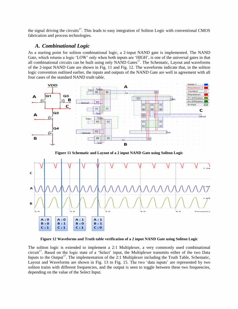
A Square wave clock signal and Soliton clock signal are launched at one end of the microstrip, and the
signals obtained at the other end are observed. In order to characterize the distortion, eye diagrams are
plotted, the Eye Diagram being a superposition of multiple cycles of a periodic signal characterizing the
variation in amplitudes, rising times etc. observed. The Eye Diagram of the Square and Soliton Clocks are
shown in Fig. 4. It is clearly seen that the distortion undergone by the square clock is considerably higher
than that of the soliton clock, both in terms of amplitude and timing jitters, clearly establishing the fact
that the soliton clock is indeed more robust than the conventional square wave clock. In addition to these
results, it has also been shown that in Terahertz frequency communication systems involving optical,
wired and wireless channels, solitons act as excellent carriers for modulation, with the bit error rate
performance easily surpassing that of the square and sine wave counterparts13,14
.
Figure 4 The Dimensions of the Microstrip; Eye Diagrams of the Square Clock (Left) and Soliton Clock
(Right)
4. Generation of Soliton Clock The generation of solitons in the proposed design is attributed to the linear and nonlinear effects arising in
the MOSFET. Of particular importance is the non-quasi static charge model of the MOS channel relevant
at high frequencies, which states that the channel of a MOSFET can be modeled as a nonlinear
transmission line. An illustration of the NQS model applied to the NMOSFET along with the drain, gate
and source capacitance is shown in Fig. 5. Also, an extension to this model gives the equivalent
representation of the nonlinear transmission line by an Elmore resistance15
. This resistance is length
dependent, which indicates the effect of wiring and transistor geometry in generation of solitons. The
equivalent circuit of Fig. 5, with the Elmore resistance denoted by „Re‟ is shown in Fig. 6. The
dependence on the Elmore Resistance on the gate-source voltage „Vgs‟ is given as follows:
)(10Re
thgsoxeffeff
eff
VVCW
L
(6)
where „μeff‟ is the effective carrier mobility, „Leff‟ and „Weff‟ denote the effective channel length and width
of the NMOS transistor, „Cox‟ denotes the oxide layer capacitance and „Vth‟ is the threshold voltage of the
transistor.
Page 5
Figure 5 Non-quasi static representation of a NMOS channel
Figure 6 Equivalent circuit of non quasi static channel effect
The basis for the generation of solitons is the application of a sinusoidal signal to a CMOS inverter, where
the nonlinearity of the MOSFET provides appropriate wave shaping and harmonic generation yielding a
train of solitons as the output. The schematic and layout is created using the Microwind software in
180nm CMOS Technology, and are illustrated in Fig. 7 and Fig. 8 along with the output voltage
waveform obtained16
.
Figure 7 Schematic and Layout of the Soliton Clock Generator as obtained from Microwind
Page 6
Figure 8 Input and Output Voltage Waveforms of the Soliton Clock Generator as obtained from Microwind
The generated soliton pulse train is verified by fitting it with a standard hyperbolic secant (sech) pulse of
a Full Width Half Maximum (FWHM) of 42ps, and this is shown in Fig. 9. It is seen that there is a
reasonably good match between the obtained output and ideal Soliton pulse.
Figure 9 Soliton Clock output from Microwind fitted to a ‘sech’ based solitary pulse
The generated soliton clock is used to formulate a return to zero logic system, where the presence of a
pulse indicates „1‟ or logic „HIGH‟ and the absence of a pulse represents „0‟ or logic „LOW‟. An example
of a bit stream using this logic convention is shown in Fig. 10.
Figure 10 Example of a Bit Stream using the Soliton Logic Convention
5. Logic Circuits using Soliton Logic In this section, various combinational and sequential logic circuits using the soliton logic are implemented
and the waveforms are characterized17
. All the implementations are performed in the 180nm CMOS
Technology using the Microwind Software, with the transistor dimension set to an aspect ratio of
400nmx200nm. A noteworthy feature about the Soliton Logic is that all the logic circuits designed use the
conventional schematics that have been used for square wave based clocks, with the only difference being
Page 7
the signal driving the circuits17
. This leads to easy integration of Soliton Logic with conventional CMOS
fabrication and process technologies.
A. Combinational Logic
As a starting point for soliton combinational logic, a 2-input NAND gate is implemented. The NAND
Gate, which returns a logic „LOW‟ only when both inputs are „HIGH‟, is one of the universal gates in that
all combinational circuits can be built using only NAND Gates17
. The Schematic, Layout and waveforms
of the 2-input NAND Gate are shown in Fig. 11 and Fig. 12. The waveforms indicate that, in the soliton
logic convention outlined earlier, the inputs and outputs of the NAND Gate are well in agreement with all
four cases of the standard NAND truth table.
Figure 11 Schematic and Layout of a 2 input NAND Gate using Soliton Logic
Figure 12 Waveforms and Truth table verification of a 2 input NAND Gate using Soliton Logic
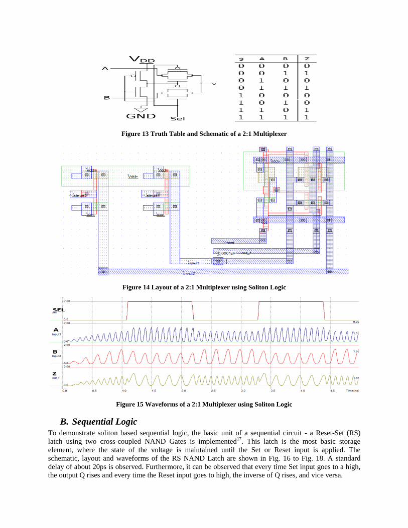
The soliton logic is extended to implement a 2:1 Multiplexer, a very commonly used combinational
circuit17
. Based on the logic state of a „Select‟ input, the Multiplexer transmits either of the two Data
Inputs to the Output17
. The implementation of the 2:1 Multiplexer including the Truth Table, Schematic,
Layout and Waveforms are shown in Fig. 13 to Fig. 15. The two „data inputs‟ are represented by two
soliton trains with different frequencies, and the output is seen to toggle between these two frequencies,
depending on the value of the Select Input.
Page 8
Figure 13 Truth Table and Schematic of a 2:1 Multiplexer
Figure 14 Layout of a 2:1 Multiplexer using Soliton Logic
Figure 15 Waveforms of a 2:1 Multiplexer using Soliton Logic
B. Sequential Logic
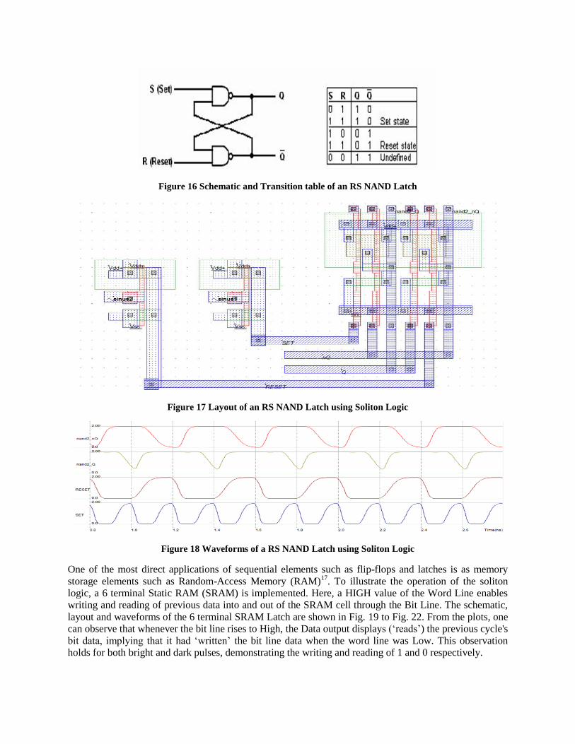
To demonstrate soliton based sequential logic, the basic unit of a sequential circuit - a Reset-Set (RS)
latch using two cross-coupled NAND Gates is implemented17
. This latch is the most basic storage
element, where the state of the voltage is maintained until the Set or Reset input is applied. The
schematic, layout and waveforms of the RS NAND Latch are shown in Fig. 16 to Fig. 18. A standard
delay of about 20ps is observed. Furthermore, it can be observed that every time Set input goes to a high,
the output Q rises and every time the Reset input goes to high, the inverse of Q rises, and vice versa.
Page 9
Figure 16 Schematic and Transition table of an RS NAND Latch
Figure 17 Layout of an RS NAND Latch using Soliton Logic
Figure 18 Waveforms of a RS NAND Latch using Soliton Logic
One of the most direct applications of sequential elements such as flip-flops and latches is as memory
storage elements such as Random-Access Memory (RAM)17
. To illustrate the operation of the soliton
logic, a 6 terminal Static RAM (SRAM) is implemented. Here, a HIGH value of the Word Line enables
writing and reading of previous data into and out of the SRAM cell through the Bit Line. The schematic,
layout and waveforms of the 6 terminal SRAM Latch are shown in Fig. 19 to Fig. 22. From the plots, one
can observe that whenever the bit line rises to High, the Data output displays („reads‟) the previous cycle's
bit data, implying that it had „written‟ the bit line data when the word line was Low. This observation
holds for both bright and dark pulses, demonstrating the writing and reading of 1 and 0 respectively.
Page 10
Figure 19 Schematic of a 6 Terminal SRAM
Figure 20 Layout of an SRAM using Soliton Logic
Figure 21 Waveforms of a SRAM using Bright Soliton based bit line, demonstrating the writing of ‘1’
Figure 22 Waveforms of a SRAM using Dark Soliton based bit line, demonstrating the writing of '0'
Page 11
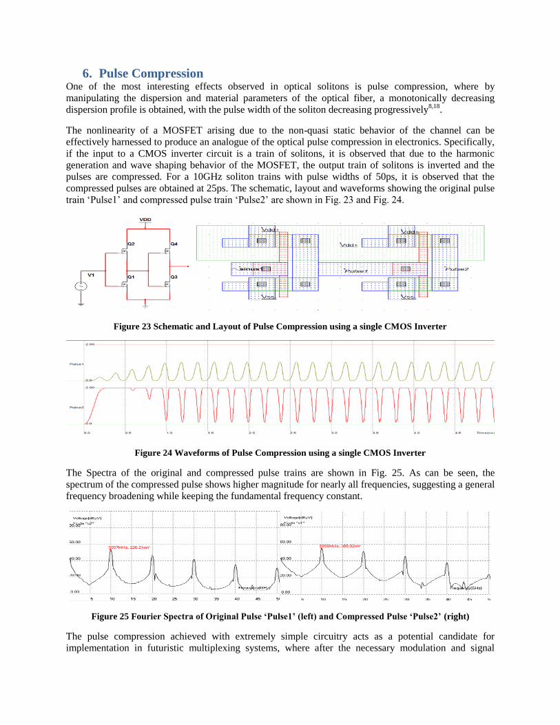
6. Pulse Compression One of the most interesting effects observed in optical solitons is pulse compression, where by
manipulating the dispersion and material parameters of the optical fiber, a monotonically decreasing
dispersion profile is obtained, with the pulse width of the soliton decreasing progressively8,18
.
The nonlinearity of a MOSFET arising due to the non-quasi static behavior of the channel can be
effectively harnessed to produce an analogue of the optical pulse compression in electronics. Specifically,
if the input to a CMOS inverter circuit is a train of solitons, it is observed that due to the harmonic
generation and wave shaping behavior of the MOSFET, the output train of solitons is inverted and the
pulses are compressed. For a 10GHz soliton trains with pulse widths of 50ps, it is observed that the
compressed pulses are obtained at 25ps. The schematic, layout and waveforms showing the original pulse
train „Pulse1‟ and compressed pulse train „Pulse2‟ are shown in Fig. 23 and Fig. 24.
Figure 23 Schematic and Layout of Pulse Compression using a single CMOS Inverter
Figure 24 Waveforms of Pulse Compression using a single CMOS Inverter
The Spectra of the original and compressed pulse trains are shown in Fig. 25. As can be seen, the
spectrum of the compressed pulse shows higher magnitude for nearly all frequencies, suggesting a general
frequency broadening while keeping the fundamental frequency constant.
Figure 25 Fourier Spectra of Original Pulse ‘Pulse1’ (left) and Compressed Pulse ‘Pulse2’ (right)
The pulse compression achieved with extremely simple circuitry acts as a potential candidate for
implementation in futuristic multiplexing systems, where after the necessary modulation and signal
Page 12
conditioning are performed the pulses can be compressed and sent through the channel, thus
accommodating more number of pulses in the same duration.
7. Conclusion The spectral profiles of conventional square clocks and Gaussian based soliton pulses are studied and
after performing transmission line based models, it is found that the solitons are indeed more robust than
square signals while passing through microstrip based interconnects. Based on these observations, a
return to zero logic based on solitons is proposed. The generation of solitons using the nonlinearity of a
single transistor is then discussed, and various combinational and sequential logic circuits using solitons
are explored, all implementations being carried out at the submicron VLSI level using 180nm CMOS
technology. Finally pulse compression of electrical solitons using a single CMOS inverter is discussed
and implemented in 180nm CMOS. The use of Soliton pulses as Clock enhancing the robustness of
propagation, coupled with the simplicity of soliton generation and implementation of logic systems
compatible with state-of-the-art CMOS technologies form the significant highlights of the present work.
References 1. A. Rostami, H. Rasooli, H. Baghban, Terahertz Technology Fundamentals and Applications, Springer,
(2011)
2. C. Caloz, S. Gupta, Q. Zhang, B. Nikfal. Analog Signal Processing. IEEE Microwave Magazine. 14, 87
(2013)
3. W. H. Chen, G. Liu, B. Zdravko, A. Niknejad. A Highly Linear Broadband CMOS LNA Employing
Noise and Distortion Cancellation. IEEE J. Solid-State Circuits, 43, 1164 (2008).
4. G. Kizer, Digital Microwave Communication: Engineering Point-to-Point Microwave Systems, Wiley,
(2013).
5. J. C. Pedro and B. C. Carvalho, Intermodulation Distortion in Microwave and Wireless Circuits, Artech
House, (2003).
6. D. M. Pozar, Microwave Engineering, Wiley, (2011).
7. K. M. Gharaibeh, Nonlinear Distortion in Wireless Systems: Modeling and Simulation with MATLAB,
Wiley, (2011).
8. Y. S. Kivshar, G. Agarwal, Optical Solitons: From Fibers to Photonic Crystals, Academic Press,
(2013).
9. V. K. Tripathi, J. B. Retti. A SPICE model for multiple coupled microstrips and other transmission
lines. IEEE Trans. Microwave Theory and Techniques. 33, 1513 (1985).
10. S. Y. Liao, Microwave Devices and Circuits, Prentice-Hall, (1985).
11. R. Gard, I. Bahl, M. Bozzi, Microstrip Lines and Slotlines, Artech House, (2013).
12. J. Brinkhoff, A. E. Parker. Effect of baseband impedance on FET intermodulation. IEEE Trans.
Microwave Theory and Techniques. 51, 1045 (2003).
13. R. Ganapathy, M. Easwaran, G. J. Raj, B. Sai Venkatesh, K. Porsezian. Modeling and evaluation of
Radio over Fiber Communication Systems on employing Nanophotonic Devices. ICONSET, 181 (2011).
14. B. Sai Venkatesh, R. Ganapathy and K. Porsezian. Design of Terahertz Radio over Fiber - Beyond
4G. WRAP, (2013).
15. M. Chan, K. Hui, C.Hu, P. K. Ko. A robust and physical BSIM3 non quasi static transient and AC
small signal model for circuit simulation. IEEE Trans. Electron Devices. 45, 834, (1998).
16. J. P. Uyemura, Chip Design for Submicron VLSI: CMOS Layout and Simulation, Thomson/Nelson
(2006).
17. R. Dueck, K. Reid, Digital Electronics, Cengage Learning, (2011).
18. K. Porsezian, R. Ganapathy, A. Hasegawa, V. N. Serkin. Nonautonomous Soliton Dispersion
Management. IEEE Quantum Electronics. 45, 1577, (2009).