International Journal of Science, Engineering and Technology Research (IJSETR), Volume 3, Issue 5, May 2014
ISSN: 2278 – 7798 All Rights Reserved © 2014 IJSETR
1241
Abstract— A comparison between different sense
amplifiers for SRAM are performed using 180nm
technology .Comparison is being made with respect to the
sensing delay , power consumption & leakage power by
varying the bit line , data line and load line capacitances
and varying the supply voltage & temperature values.
Effect of these design parameters on the different sense
amplifiers has been analyzed. Comparisons are being
carried out in Cadence gpdk 180nm technology.
Index Terms— VLSA, CLSA, Conventional, PBT,
SFT,
Clamped Bit line, Hybrid Current Sense Amplifiers
I. INTRODUCTION
SRAMs are used as cache memory hence it must perform at
high speed for both read & write operations along with low
power consumption. But memory and its peripheral circuits
can adversely affect the overall speed and power of the
system. Among all the peripherals of a SRAM memory, sense
amplifier plays a major role .It is used to sense or read the
data stored or written onto the selected memory bit. The
performance of sense amplifiers [1] strongly affects both
memory access time and overall power consumption. As the
memory capacity is increasing according to the demand for
large memory size it give rise to large bit line capacitance
which in turn makes memory slower and more energy
hungry.
A sense amplifier plays the role of sensing the differential
voltage generated on the bit line or bit line according to the
data stored in the memory and accordingly convert the data
stored on the bit line/bit line bar to full logic level „1„ or „0‟
which can be read at the output stage . When a memory cell is
being accessed for read operation current "IDATA" is
produced which removes some of the stored charge (dQ)
from the precharged bit lines. Since the bit lines are very
long, and are shared by other similar memory cells, the
parasitic capacitance "CBL" & resistance "RBL" are also
large. Hence, the bit line voltage swing (dVBL) caused by the
removal of "dQ" from the bit line is very small dVBL = Q/CBL.
Sense amplifier is thus used to convert this small voltage
swing to a full logic signal.
To improve the speed & overall performance of memory it is
necessary to understand & analyze different types of sense
amplifiers .According to the demand of situation appropriate
sense amplifier must be used as every design has its own
advantage & disadvantage.
Sense amplifiers are classified on the basis of :-
1)Circuit Types -- differential and non differential
2)Operation Modes -- voltage, current and charge amplifiers.
A differential sense amplifier distinguishes small signals
from noise and starts signal detection faster when compared
to non differential sense amplifier .Even though differential
sensing requires extra silicon area yet in most of the design
the use of differential amplifier allows to combine very high
packaging density with reasonable access time and low
power consumption. The rest of the paper is organized as
follows. Section 2 describes the different sense amplifiers,
Section 3 describes the comparative study of different sense
amplifiers & Section 4 describes the conclusion of this
paper.
II. LITERATURE SURVEY OF VARIOUS SENSE AMPLIFIERS
Differential sense amplifier may be classified as:
1. Voltage sense amplifier
2. Current sense amplifier
3. Charge transfer sense amplifier (CTSA)
The simplest voltage sense amplifier [2] is the differential
couple. When a cell is being read, a small voltage swing
appears on the bit line which is further amplified by
differential couple and use to drive digital logic. However the
bit line voltage swing is becoming smaller and is reaching
the same magnitude as bit line noise, the voltage sense
amplifier become unusable.
The fundamental reason for applying current mode sense
amplifier in sense circuit is their small input impedances.
Benefits of small input and output impedances are reductions
in sense circuit delays, voltage swings, cross-talking,
substrate currents and substrate voltage modulations.
The operation of the CTSA is based on the charge re
distribution mechanism between very high bit line
capacitance and low output capacitance of the sense
amplifier. A differential charge transfer amplifier takes
advantage of the increased bit-line capacitance and also
offers a low-power operation without sacrificing the speed.
A. Voltage sense amplifier
The voltage sense amplifier can be classified as follows
1. Basic differential voltage amplifier.
Review of Different Sense Amplifiers For
SRAM in 180nm Technology
Geeta Pattnaik, Sweta Padma Dash, Komal Priyadarshini, Adyasa Samantaray, Adyasha Rath
International Journal of Science, Engineering and Technology Research (IJSETR), Volume 3, Issue 5, May 2014
ISSN: 2278 – 7798 All Rights Reserved © 2014 IJSETR
1242
2. Simple differential voltage sense amplifier.
3. Full complementary differential voltage sense amplifiers
4. Positive feedback differential voltage sense amplifiers.
5. Full complementary positive feedback voltage sense
amplifiers.
There are many ways to enhance the performance of various
voltage sense amplifiers by adding a few devices to the
differential voltage sense amplifier. These ways are :-
1. Decoupling of bit lines from the sense amplifiers
temporarily.
2. The input and outputs in feedback sense amplifiers can be
separated.
3. Constant current source are applied to the source devices,
4. output signal amplitude can be optimized .
Methods (1) & (2) tends to decrease the capacitive load of
sense amplifier. In Method (3) the sense amplifier source
resistance is virtually increased to achieve high gain, and by
approach (4) amount of switched charges is decreased.
Voltage Sense Amplifier
A voltage sense amplifier [12-13] senses the differential
voltage on the bit-lines and generates a full rail output. Fig. 1
shows the voltage sense amplifier.
Fig. 1 Voltage Latch Sense Amplifier
The design operates basing on the differential voltage
developed on its internal nodes by the input bit lines. During
the active mode when sense amplifier is triggered transistor
M7 is off and pass transistors M1 and M4 are on. As the
differential develops on the bit lines, it does so too on the
internal nodes of the sense amplifier „sol‟ and „sor‟. When
the sense signal „saenb‟ is asserted, the cross-coupled
inverters formed of M2-M5 and M3-M6 amplifies this
differential voltage to its full-swing output.
B. Current Sense Amplifier
Current sense amplifiers can be broadly classified as:
1. Conventional current mode sense amplifier
2. Current latch sense amplifier
3. Clamped bit line sense amplifier
4. Simple 4T sense amplifier
5. PMOS bias type sense amplifier
6. Hybrid current sense amplifier
1) Conventional current mode sense amplifier
The design of the sense amplifier [4] is based on the classic
cross-coupled latch structure (M4-M7). An extra NMOS
transistor (M8) is used for sense amplifier activation and
transistors (Ml-M3) are used to equalize the bit line pair..
The sense amplifier operates in 2 phases: precharge &
sensing and amplifying the sensed signal. During the
precharge phase the EQ signal goes low and the bit-lines are
precharged to VDD. During the sensing phase the EQ and
EN signals are high which activates the cross-coupled
structure and pulls the outputs to the appropriate full logic
level. Conventional current mode sense amplifiers are
suitable for realizing high speed and large size memories.
Since large voltage swing on the bit-lines is not required this
sense amplifier can be suitable for low voltage operation,
However the performance of the sense amplifier depends
strongly on CBL, because output node is loaded with bitline
capacitance. The performance degrades at low voltage
operation i.e., at supply voltages less than1.5V).
Fig. 2 Conventional Current Mode Sense Amplifier
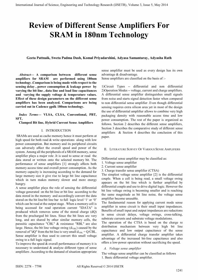
2) Current latch sense amplifier
The operation of this sense amplifier[12-13] is based on
the differential current produced by transistors M9 and
M10 in the two pull down branches of the sense
amplifier. At the activation of the read operation, either
one of the „bit line‟ or „bit line bar‟ inputs is
lowered depending on the data stored in the cell. When
the sense amplifier is activated by pulling down the input
„saenb‟, transistor M11 turns on and the precharge
transistors are simultaneously turned off. The channel
International Journal of Science, Engineering and Technology Research (IJSETR), Volume 3, Issue 5, May 2014
ISSN: 2278 – 7798 All Rights Reserved © 2014 IJSETR
1243
current of M9 and M10 become unequal since their gate
voltages differ by the generated bit line differential
voltages. The current thus flowing in the two branches of
the sense amplifier are unequal and the voltage at either
„out‟ or „outb‟ falls faster than the other node. This
difference in voltage is resolved by the cross-coupled
inverters formed of M2, M6 and M3, M7.
Fig. 3 Current Latch Sense Amplifier
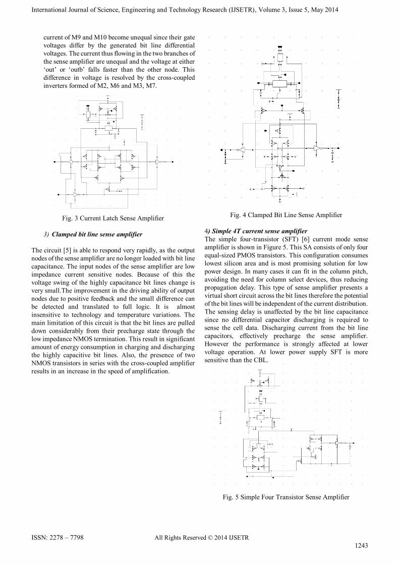
3) Clamped bit line sense amplifier
The circuit [5] is able to respond very rapidly, as the output
nodes of the sense amplifier are no longer loaded with bit line
capacitance. The input nodes of the sense amplifier are low
impedance current sensitive nodes. Because of this the
voltage swing of the highly capacitance bit lines change is
very small.The improvement in the driving ability of output
nodes due to positive feedback and the small difference can
be detected and translated to full logic. It is almost
insensitive to technology and temperature variations. The
main limitation of this circuit is that the bit lines are pulled
down considerably from their precharge state through the
low impedance NMOS termination. This result in significant
amount of energy consumption in charging and discharging
the highly capacitive bit lines. Also, the presence of two
NMOS transistors in series with the cross-coupled amplifier
results in an increase in the speed of amplification.
Fig. 4 Clamped Bit Line Sense Amplifier
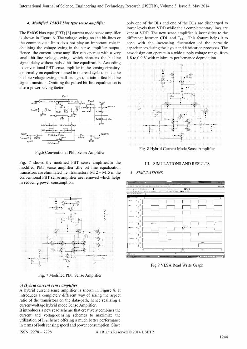
4) Simple 4T current sense amplifier
The simple four-transistor (SFT) [6] current mode sense
amplifier is shown in Figure 5. This SA consists of only four
equal-sized PMOS transistors. This configuration consumes
lowest silicon area and is most promising solution for low
power design. In many cases it can fit in the column pitch,
avoiding the need for column select devices, thus reducing
propagation delay. This type of sense amplifier presents a
virtual short circuit across the bit lines therefore the potential
of the bit lines will be independent of the current distribution.
The sensing delay is unaffected by the bit line capacitance
since no differential capacitor discharging is required to
sense the cell data. Discharging current from the bit line
capacitors, effectively precharge the sense amplifier.
However the performance is strongly affected at lower
voltage operation. At lower power supply SFT is more
sensitive than the CBL.
Fig. 5 Simple Four Transistor Sense Amplifier
International Journal of Science, Engineering and Technology Research (IJSETR), Volume 3, Issue 5, May 2014
ISSN: 2278 – 7798 All Rights Reserved © 2014 IJSETR
1244
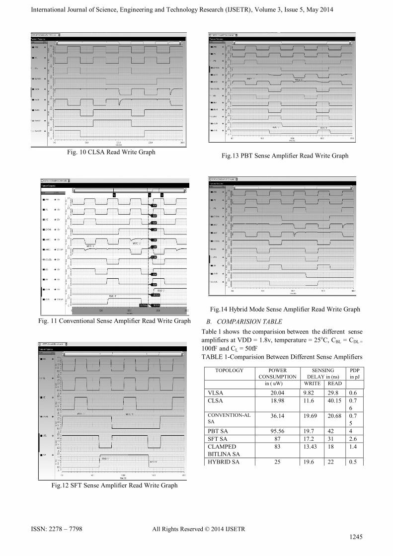
4) Modified PMOS bias type sense amplifier
The PMOS bias type (PBT) [6] current mode sense amplifier
is shown in Figure 6. The voltage swing on the bit-lines or
the common data lines does not play an important role in
obtaining the voltage swing in the sense amplifier output.
Hence the current sense amplifier can operate with a very
small bit-line voltage swing, which shortens the bit-line
signal delay without pulsed bit-line equalization. According
to conventional PBT sense amplifier in the sensing circuitry,
a normally-on equalizer is used in the read cycle to make the
bit-line voltage swing small enough to attain a fast bit-line
signal transition. Omitting the pulsed bit-line equalization is
also a power-saving factor.
Fig.6 Conventional PBT Sense Amplifier
Fig. 7 shows the modified PBT sense amplifier.In the
modified PBT sense amplifier ,the bit line equalization
transistors are eliminated i.e., transistors M12 – M15 in the
conventional PBT sense amplifier are removed which helps
in reducing power consumption.
Fig. 7 Modified PBT Sense Amplifier
6) Hybrid current sense amplifier
A hybrid current sense amplifier is shown in Figure 8. It
introduces a completely different way of sizing the aspect
ratio of the transistors on the data-path, hence realizing a
current-voltage hybrid mode Sense Amplifier.
It introduces a new read scheme that creatively combines the
current and voltage-sensing schemes to maximize the
utilization of Icell, hence offering a much better performance
in terms of both sensing speed and power consumption. Since
only one of the BLs and one of the DLs are discharged to
lower levels than VDD while their complementary lines are
kept at VDD. The new sense amplifier is insensitive to the
difference between CDL and CDL . This feature helps it to
cope with the increasing fluctuation of the parasitic
capacitances during the layout and fabrication processes. The
new design can operate in a wide supply voltage range, from
1.8 to 0.9 V with minimum performance degradation.
Fig. 8 Hybrid Current Mode Sense Amplifier
III. SIMULATIONS AND RESULTS
A. SIMULATIONS
Fig.9 VLSA Read Write Graph
International Journal of Science, Engineering and Technology Research (IJSETR), Volume 3, Issue 5, May 2014
ISSN: 2278 – 7798 All Rights Reserved © 2014 IJSETR
1245
Fig. 10 CLSA Read Write Graph
Fig. 11 Conventional Sense Amplifier Read Write Graph
Fig.12 SFT Sense Amplifier Read Write Graph
Fig.13 PBT Sense Amplifier Read Write Graph
Fig.14 Hybrid Mode Sense Amplifier Read Write Graph
B. COMPARISION TABLE
Table 1 shows the comparision between the different sense
amplifiers at VDD = 1.8v, temperature = 25oC, CBL = CDL =
100fF and CL = 50fF
TABLE 1-Comparision Between Different Sense Amplifiers
TOPOLOGY POWER
CONSUMPTION
SENSING
DELAY in (ns)
PDP
in pJ
in ( uW) WRITE READ
VLSA 20.04 9.82 29.8 0.6
CLSA 18.98 11.6 40.15 0.7
6 CONVENTION-AL
SA 36.14 19.69 20.68 0.7
5
PBT SA 95.56 19.7 42 4
SFT SA 87 17.2 31 2.6
CLAMPED
BITLINA SA
83 13.43 18 1.4
HYBRID SA 25 19.6 22 0.5
International Journal of Science, Engineering and Technology Research (IJSETR), Volume 3, Issue 5, May 2014
ISSN: 2278 – 7798 All Rights Reserved © 2014 IJSETR
1246
Fig. 15 PDP Graph Of The Sense Amplifiers
IV. CONCLUSION
The obvious advantage of VLSA over the CLSA is the
requirement of lower number of transistors which means
faster access and smaller footprint. But the challenge in using
this topology has been the race condition for isolation signal
that decouples the sense amplifier bit line from the array bit
line. If the sense amplifier is enabled while M1 and M4 are
on, the memory bit line (bit or bit bar) could be discharged to
logic 0. In traditional designs, a different signal other than
sen (isolate) is used to control M1 and M4 which makes it
hard to match sense and isolate operation, but for our design
we used the same signal that enable the sense amplifier to
isolate the array bit lines. The PDP value of VLSA topology
is better than CLSA but only due to the race condition
problem seen and requirement of enough differential voltage
on the bit line pair, we go for current mode sense amplifiers
.The current mode sense amplifiers sense and operate
accordingly basing upon the differential current generated on
the bit line pair instead of differential voltage which results
in reduction in power consumption. From the PDP results
shown in table 1,we can conclude that hybrid mode sense
amplifier is the best option for both high speed and low power
sense amplifier .
ACKNOWLEDGMENT
The authors would like to thank the faculties of KIIT
University for their continuous support and guidance. The
authors would also like to thank KIIT University, Odisha for
providing the necessary tools & software for carrying out the
analysis and simulation of the paper.
REFERENCES
[1] E. Seevinck, P. van Beers, and H. Ontrop, “Current-mode techniques for
high-speed vlsi circuits with application to current sense amplifier for CMOS
SRAM‟s,” IEEE J. Solid-State Circuits, vol. 26, no. 4, pp.525–536, Apr. 1991
[2] A. Hajimiri and R. Heald, Design Issues in Cross-Coupled Inverter Sense
Amplifier. New York, 1998, pp. 149–152.
[3]A.-T. Do, S. J. L. Yung, K. Zhi-Hui, K.-S. Yeo, and L. J. L. Yung, “A full
current-mode sense amplifier for low-power SRAM applications,” in Proc.
IEEE Asia Pacific Conf. on Circuits Syst., 2008, pp. 1402–1405.
[4]Comparative study of different current mode sense amplifiers in submicron
CMOS technology A. Chrysanthopoulos, Y. Moisiadis, Y. Tsiatouhas and A.
Arapoyanni.,pp-154-159 IEEE Proc.-Circuits Devices Syst., Vol. 149, No. 3,
June 2002.
[4]Uetake, T., Maki, Y., Nakadai, T., Yoshida, K., Susuki, M., And Nanjo, R.:
„A 1.0ns access 770MHz 36kb SRAM macro‟ Symposium on VLSI Circuits:
Digest of Technical Papers, 1999.
[5]Blalock, T.N., And Jaeger, R.C.: „A high-speed clamped
bit-line current-mode sense amplifier‟, IEEE J. Solid-State Circuits,
[6]Sasaki, K., Ishibashi, K., Ueda, K., Komiyaji, K., Yamanaka, T.,
Hashimoto, N., Toyoshima, H., Kojima, F., And Shimizu, A,: „A 7-11s
140-mW I-Mb CMOS SRAM with current sense amplifier‟. ZEEE J.
Solid-State Circuits, 1992.
[7]Toumazou. C., Lidgey, Fj.J., And Haigh, D.G.: „Analogue IC
design: The current-mode approach‟ (Peter Peregrinus Ltd., London,
UK, April 1990)
[8]Seki, T., Itoh, E., Furukawa, C., Maeno, I., Ozawa, T., Sano, H., And
Suzuki, N.: „A 6-11s 1-Mb CMOS SRAM with latched sense amplifier‟. IEEE
J. Solid-State Circuits. 1993.
[9]Chun L. H and Mean Hom Ho, "High-Speed Sense Amplifier For Sram
Applications", IEEEXplore, pp. 577 - 580,2004.
[10]Baker Mohammad, Martin Saint-Laurent, Paul Bassett, and Jacob
Abraham. Cache Design for Low Power and High Yield, IEEE
International Symposium on Quality Electronic Design (ISQED) ,March
2008, pp 103-107, San Jose, CA, USA
[11]Baker Mohammad, Jacob Abraham; A reduced Voltage Swing Circuit
Using A single Supply to Enable Lower Voltage Operation for SRAMbased
Memory; Microelectronics journal, Elsevier, December 2011
[12]N. Shibata, “Current sense amplifiers for low-voltage memories,” IEICE
Trans. Electron, vol. 79, pp.1120–1130, Aug. 1996.
Ms. Geeta Pattnaik She is currently
pursuing M-Tech in VLSI and
Embedded system at KIIT University
, Odisha.. She had completed her
B.Tech from Seemanta Engineering
College affiliated to Biju Pattnaik
University and Technology in the year
2011 in the stream of Electronics &
Telecommunication. Her area of
interest is low power, high speed
digital VLSI circuit design & mixed
signal ICs. .
Ms. Sweta Padma Dash. She is
currently pursuing Master in VLSI
and Embedded system at KIIT
University , Odisha. She had
completed B.Tech from Modern
Institute of Technology and
Management, affiliated to Biju
pattnaik University and Technology
in the year 2012. Her areas of interest
include analog and mixed signal ICs.
Ms. Komal Priyadarshini. She is
currently pursuing Master in VLSI
and Embedded system at KIIT
University , Odisha. She had
completed B.Tech from Konark
Institute Of Science & Technology,
affiliated to Biju pattnaik University
and Technology in the year 2011. Her
areas of interest include digital VLSI.
International Journal of Science, Engineering and Technology Research (IJSETR), Volume 3, Issue 5, May 2014
ISSN: 2278 – 7798 All Rights Reserved © 2014 IJSETR
1247
Ms. Adyasa Samantaray She has
received her B.Tech degree from Biju
Pattnaik University of Technology in
the year 2009 in Applied Electronics
& Instrumentation Engineering. She
is presently pursuing her M.Tech at
KIIT University with specialization in
VLSI & Embedded System. Her areas
of interest include high speed, low
power digital and analog design.
Ms. Adyasha Rath. She is presently
pursuing her M.Tech with
specialization in VLSI & Embedded
Systems under KIIT University. She
has received her B.Tech degree from
Biju Pattnaik University of
Technology in Electronics &
Communication Engineering in the
year 2012. Her areas of interest
include low power, high speed analog
and mixed mode circuit design.