34 JOHNS HOPKINS APL TECHNICAL DIGEST, VOLUME 20, NUMBER 1 (1999) AND M Some Key Issues in Microelectronic Packaging Guy V. Clatterbaugh, Paul Vichot, and Harry K. Charles, Jr. ilitary and space electronics are tending toward increased system perfor- mance, i.e., higher speed, higher circuit density, and higher functionality. Recent reductions in government spending on space and military hardware have also made cost reduction a key consideration. As electronics approach physical size and performance limits, practical considerations such as wireability, thermal management, electromagnetic compatibility, and system reliability become dominant issues in system design. Resolving such issues requires the use of sophisticated analysis and computational methods. (Keywords: Electronic packaging, Multiconductor transmission line analysis, Printed circuit board thermal analysis, Wireability.) INTRODUCTION In recent years, the electronics industry has discov- ered that the major economic advances made in high- performance electronic circuitry have come with in- creased integration. The industry is rapidly converging toward true wafer-scale integration, i.e., toward an entire system fabricated on one silicon substrate. Every 5 years or so, we see wafer foundries processing larger silicon wafers with smaller line geometries. Today, 12- in. wafers are being processed with 0.35-mm lines. By the year 2010, 16-in. wafers and 0.10-mm lines will likely be the standard. Even with the increased ability to build larger chips with greater functionality, very few systems function as a single chip. Instead, the trend is to take advantage of recent technology advances in electronic packaging to pack chips side by side, sometimes even in three- dimensional stacks, to achieve still higher levels of functionality and performance while reducing volume and weight. The quest to achieve better performance (higher speed and integration) has placed pressure on manu- facturers and has forced integrated circuits (ICs) closer together. High-speed computer systems require that the central processing unit and the memory and con- trollers be proximal to minimize interconnection de- lays. The increased functionality of these chips has increased the number of inputs and outputs (I/Os). This, in turn, has imposed routing demands that have changed the way we think about fabricating printed wiring boards (PWBs) and building IC packages. The higher speeds and higher densities also create thermal and thermal stress problems that challenge the limits of today’s microelectronic materials and manufactur- ing methods.
Transcript
G. V. CLATTERBAUGH, P. VICHOT, AND H. K. CHARLES, JR.
M
Some Key Issues in Microelectronic Packaging
Guy V. Clatterbaugh, Paul Vichot, and Harry K. Charles, Jr.
ilitary and space electronics are tending toward increased system perfor-mance, i.e., higher speed, higher circuit density, and higher functionality. Recentreductions in government spending on space and military hardware have also madecost reduction a key consideration. As electronics approach physical size andperformance limits, practical considerations such as wireability, thermal management,electromagnetic compatibility, and system reliability become dominant issues insystem design. Resolving such issues requires the use of sophisticated analysis andcomputational methods.(Keywords: Electronic packaging, Multiconductor transmission line analysis, Printedcircuit board thermal analysis, Wireability.)
INTRODUCTIONIn recent years, the electronics industry has discov-
ered that the major economic advances made in high-performance electronic circuitry have come with in-creased integration. The industry is rapidly convergingtoward true wafer-scale integration, i.e., toward anentire system fabricated on one silicon substrate. Every5 years or so, we see wafer foundries processing largersilicon wafers with smaller line geometries. Today, 12-in. wafers are being processed with 0.35-mm lines. Bythe year 2010, 16-in. wafers and 0.10-mm lines willlikely be the standard.
Even with the increased ability to build larger chipswith greater functionality, very few systems function asa single chip. Instead, the trend is to take advantageof recent technology advances in electronic packagingto pack chips side by side, sometimes even in three-dimensional stacks, to achieve still higher levels of
34 JOH
functionality and performance while reducing volumeand weight.
The quest to achieve better performance (higherspeed and integration) has placed pressure on manu-facturers and has forced integrated circuits (ICs) closertogether. High-speed computer systems require thatthe central processing unit and the memory and con-trollers be proximal to minimize interconnection de-lays. The increased functionality of these chips hasincreased the number of inputs and outputs (I/Os).This, in turn, has imposed routing demands that havechanged the way we think about fabricating printedwiring boards (PWBs) and building IC packages. Thehigher speeds and higher densities also create thermaland thermal stress problems that challenge the limitsof today’s microelectronic materials and manufactur-ing methods.
NS HOPKINS APL TECHNICAL DIGEST, VOLUME 20, NUMBER 1 (1999)
In this era of dwindling federal budgets, cost is amajor concern. Previously, high performance and highreliability were demanded of military and space elec-tronic systems; cost was often not an issue. However,the military now mandates as much use of commercialoff-the-shelf hardware as possible, and the watchwordfrom NASA is “smaller, lighter, and cheaper.” So whilethe emphasis on cost has increased, the emphasis onperformance and reliability has remained high. Withthis heightened demand for more complexity, cost-reduction opportunities are being strained.
The primary objective of microelectronic packagingis to design an electronic system that will satisfy therequirements for a particular application at a reason-able cost. Because of the many options available tointerconnect and house an electronic system, thechoice of a packaging technology for a given applica-tion is not always straightforward. Selection criteriamay include one or more technology drivers:
These fundamental design considerations affectspeed, functionality, junction temperatures, volume,and weight. The primary goal is to select the most cost-effective yet reliable interconnection technology,which requires a quantification of the technologydrivers. The resolution of these key design issues oftendepends on the use of sophisticated analysis methods.
This article discusses some of the quantitative toolsdeveloped and used at APL to assist the electronicpackaging engineer in selecting reliable, cost-effectivesolutions for packaging high-performance electronicsystems. After briefly examining various packagingoptions, we will detail five of the seven selection cri-teria already noted: wireability, yield, cost, heat trans-fer, and electromagnetic performance.
MICROELECTRONIC PACKAGINGOPTIONS
Microelectronic packaging is a branch of engineer-ing that deals with the design of methods for the fab-rication and manufacture of interconnected miniatureelectronic systems (e.g., ICs and discrete and integrat-ed passive devices) and the reliability of those systems.Specifically, microelectronic packaging involves rout-ing signals while maintaining signal integrity, dis-tributing ground and power to ICs, dispersing dissipat-ed thermal energy while maintaining structural and
JOHNS HOPKINS APL TECHNICAL DIGEST, VOLUME 20, NUMBER 1 (
SOME KEY ISSUES IN MICROELECTRONIC PACKAGING
material integrity, and protecting the circuit from en-vironmental hazards.
Almost all of the methods for packaging ICs includethe use of a PWB with connectors that provide thereal-world I/Os to an electronic circuit. The traditionalpackaging approach involves the use of single packag-es. The chief advantage of single-chip packages is theability to fully test the IC before interconnecting it tothe underlying substrate. Such packaged devices areeither through-hole mounted or surface mounted tothe PWB.
Surface-mounted components do not require viaholes to go through the entire board. Instead, packagesand other surface-mounted components can be sol-dered to both sides of the PWB, thereby increasingcircuit density. This approach is called surface-mounttechnology (SMT). The addition of area-array–stylepackages such as ball-grid arrays (BGAs) and chip-scale packages (CSPs) is making SMT competitivewith the highest-density packaging technologies, al-though the reliability of some area-array packages isstill questionable.
A newer packaging technology involves the attach-ment of more than one device onto a high-densityinterconnection substrate, which is then mounted ina large package. This provides both I/O pins and en-vironmental protection. This so-called multichip mod-ule (MCM) technology is further characterized by thesubstrate technologies used to interconnect the at-tached ICs.
MCM-D represents thin film “deposited” metal anddielectric multilayers. MCM-D substrates have thehighest wiring densities of all MCM technologiesowing to the sophisticated semiconductor processingequipment used to manufacture them. MCM-C refersto multilayered “ceramic” substrates, fired from stackedalternating layers of screened metal inks and unfiredceramic sheets. This technology yields a moderatelydense wiring capacity. MCM-L refers to multilayersubstrates made from stacked, metallized PWB “lami-nates,” which are individually patterned and then lam-inated. Once considered a low-density interconnecttechnology, MCM-L is rapidly approaching the densityof MCM-C and MCM-D technologies.
Direct chip attach (DCA) or chip-on-board(COB) technology entails mounting the ICs directlyto the PWB. A plastic encapsulant, which is “globbed”over the bare IC and then cured, provides environmen-tal protection. ICs can be interconnected to the sub-strate using either flip-chip, tape-automated bonding,or wire bonding methods. DCA technology is partic-ularly economical for systems that are limited to 10 orfewer ICs, since larger numbers of chips can affectsystem yield and DCA assemblies can be difficult torework.
1999) 35
G. V. CLATTERBAUGH, P. VICHOT, AND H. K
An advantage common to boththe DCA and MCM packagingoptions is the elimination of theIC package interconnection level,which allows closer proximity(shorter propagation delays) andreduced lead inductance. The pri-mary disadvantage with both meth-ods is the difficulty in purchasingfully tested ICs (the “known gooddie” problem; see the section enti-tled Yield). Other disadvantages of DCA and MCM-L technologies include poor thermal managementowing to the low thermal conductivity of PWB lam-inates and a poor coefficient of thermal expansionmatch between the die and the substrate. Solving thelast problem usually requires an interposer substratesuch as molybdenum for wire bonded die and anunderfill epoxy for flip-chip die.
The multichip carrier module (MCCM, Fig. 1)attempts to marry all the positive aspects of DCA withMCM technology. The MCCM is simply a small MCMon a thin metal carrier that can be bonded or mechan-ically attached to a PWB. The metal bottom acts asboth a heat spreader and a stress interposer for theMCM substrate. The MCCM has peripheral leads forwire bonding, soldering, or tab bonding to a PWB. Thebare ICs are protected using a glob-top material.
We return now, for the remainder of this article, toa discussion of some key issues in the selection ofpackaging technologies and an examination of quan-titative tools used to analyze them at APL.
SELECTION CRITERIA ANDANALYSIS
WireabilityThe objective of a wireability analysis is to deter-
mine, before layout, the ability to route a PWB. Oftenthe board size is fixed for a particular application, andthe board cost may be constrained as well. Wiringanalysis can predict the number of layers required towire the components for a particular circuit design andascertain the routability of high I/O, single-chip pack-ages. Since the routing effort and the layer count aredirectly proportional to board cost, wireability analysisis a useful tool for projecting substrate cost.
Basic Wireability Concepts
The basic concepts behind wireability analysis in-clude wiring demand, wiring capacity, average wirelength, and connectivity. Wiring demand D is theamount of wiring required to interconnect a givencircuit. Wiring capacity C is the amount of wiring
Figure 1. High-den
36
. CHARLES, JR.
sity surface-mount assembly with multichip carrier modules.
JO
available for interconnection. Wiring demand is relat-ed to wiring capacity through the equation
D = «C , (1)
where « is wiring efficiency. Typically, wiring efficiencyis near 50%, since a substrate cannot be wired using100% of its available capacity.
Wiring capacity, which is a function of the minimumsignal line pitch Ps that can be fabricated on a givensubstrate technology, is usually normalized to a givensquare dimension such as 1 in. or 1 cm. Sometimes itis normalized to the size of pitch Pp of the chip carrierpackages or bare die attached to the PWB. In this case(neglecting via holes and through-holes), for N, signallayers, the total wiring capacity C, is given by
C, = PpN,/Ps . (2)
To obtain the wiring demand, we must estimate theaverage length L per interconnection. This lengthbetween any two points is not “as the crow flies,” sincealternate layers of signal line are usually routed in x ory orthogonal streets. This length is sometimes referredto as the Manhattan length, which is given by|x1 2 x2| 1 |y1 2 y2|. The wiring demand is simplythe number of pin-to-pin connections Npp times theaverage wiring length L. If we consider that for anaverage of Npins number of pins per net there are(Npins 2 1)/Npins number of wires, then for NI/Os num-ber of I/Os, the wiring demand is simply
D =N
NN L .pins
pinsI/Os
−
1
(3)
To estimate average wire length, Rose et al.1 assumethat chips on a substrate interact with their nearestneighbors or second-nearest neighbors. This yieldsan average length of L = (Pp 1 2Pp)/2 = 1.5Pp.Rickerts2 estimates this length to be approximatelyL = 0.77P Np chips
. ,0 245 where Nchips is the number of chipsto be interconnected.
HNS HOPKINS APL TECHNICAL DIGEST, VOLUME 20, NUMBER 1 (1999)
SOME KEY ISSUES IN MICROELECTRONIC PACKAGING
Rent’s Rule
Estimating the wiring demand in the absence of apreliminary layout requires the use of Rent’s Rule,which is given by the relation
NI/Os = agb , (4)
where
NI/Os = number of chip, package, or substrate I/Osg = number of circuits contained within the chip,
package, or substrate,a = Rent’s coefficient, or the average number of
connections per circuit or I/O, andb = Rent’s exponent.
Approximate Rent’s Rule exponents and coefficientsfor various devices are given in Table 1.
Rent’s Rule is especially useful in determining re-quired circuit density and optimal device placementfor a particular circuit design. In the following exam-ple, we extend the model described by Schmidt3 for aPWB with an I/O connector on one edge to estimatethe maximum wiring required by a four-sided MCMwith I/Os on all sides. The total number of gates (orcircuits) G on an MCM containing an arbitrary num-ber of circuits can be found from the relation
G = N gi ii =
m,
1∑ (5)
where Ni is the number of type i components, and mis the number of different devices. (This assumes thatall of the circuits have the same Rent’s relationship).The total package I/O count NI/Os, assuming no inter-action between circuits of different types (a worst-casewiring scenario), is given by
Table 1. Rent’s Rule coefficients and exponents forvarious device technologies.
JOHNS HOPKINS APL TECHNICAL DIGEST, VOLUME 20, NUMBER 1 (1
NI/Os = aGb . (6)
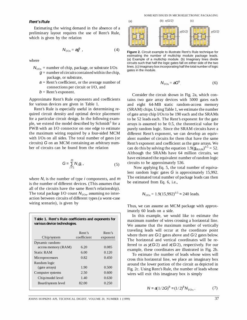
Consider the circuit shown in Fig. 2a, which con-tains two gate array devices with 5000 gates eachand eight 64-MB static random-access memory(SRAM) chips. Using Table 1, we estimate the numberof gate array chip I/Os to be 190 each and the SRAMsto be 52 leads each. The Rent’s exponent for the gatearrays is assumed to be 0.5, the theoretical value forpurely random logic. Since the SRAM circuits have adifferent Rent’s exponent, we can develop an equiv-alent number of circuits for them that have the sameRent’s exponent and coefficient as the gate arrays. Wecan do this by solving the equation 1.9(gSRAM)0.5 = 52.Although the SRAMs have 64 million circuits, wehave estimated the equivalent number of random logiccircuits to be approximately 536.
Now applying Eq. 5, the total number of equiva-lent random logic gates G is approximately 15,992.The estimated total number of package leads can thenbe estimated from Eq. 6, i.e.,
NI/Os = 1.9(15,992)0.5 ≈ 240 leads.
Thus, we can assume an MCM package with approx-imately 60 leads on a side.
In this example, we would like to estimate themaximum number of wires crossing a horizontal line.We assume that the maximum number of verticallytraveling leads will occur at the coordinate pointwhere there are G/2 gates above and G/2 gates below.The horizontal and vertical coordinates will be re-ferred to as y(G/2) and x(G/2), respectively. For ourexample, these coordinates are illustrated in Fig. 2b.
To estimate the number of leads whose wires willcross this horizontal line, we place an imaginary boxaround the lower portion of the circuit as depicted inFig. 2c. Using Rent’s Rule, the number of leads whosewires will exit this imaginary box is simply
N = a G Nb b(1/ ) ( / ) .I/Os2 1 2= (7)
Figure 2. Circuit example to illustrate Rent’s Rule technique forestimating the number of multichip module package leads.(a) Example of a multichip module. (b) Imaginary lines dividecircuits such that half the logic gates fall on either side of the twolines. (c) Imaginary box incorporating half the total number of logicgates in the module.
(a) (b) (c)x(G/2)
y(G/2) y(G/2)
999) 37
3
G. V. CLATTERBAUGH, P. VICHOT, AND H. K. CHARLES, JR.
Also, since we can assume that the number of leadsleading to the package I/O pins located beneath thisline will not affect the wire congestion in the verticaldirection, we must reduce the number of package leadsby a factor of (1 – N9I/Os/NI/Os), where N9I/Os is thenumber of package leads available to the G/2 circuitswithout crossing over the imaginary line y(G/2). Thus,the maximum number of vertically going leads can begiven by
N = NN
Nb
h I/OsI/Os
I/Os
(1/ ) .21 − ′
(8)
The number of wires crossing that horizontal line Whis given by
W = aNh h . (9)
In our example, the number of package leads N9Leadsavailable without crossing the line G/2 is 120. There-fore, assuming an average of 1.9 leads per the maxi-mum number of vertically going wires crossing thehorizontal line y(G/2), the number of wires is estimat-ed to be 161. By the symmetry of this particular ex-ample, the maximum number of horizontally travelingwires crossing the vertical line x(G/2) would also be161. If the module substrate is approximately 1.5 in.wide and the line-to-line pitch is 10 mils, then thewiring capacity is 150 wires per layer. However, withan assumed routing efficiency of 50%, the actual wir-ing capacity is 75 lines per layer. Thus, for a total of322 wires, at least five signal layers would be requiredto route this design.
Ball-Grid Array Package
A BGA package has an advantage over quad flatpacks in that its component footprint will grow moreslowly with pin count. This increase in package pindensity, however, can severely impact the routabilityof the PWB, as we will now show.
As a measure of wireability, we use the average wireor trace length L. It has been shown that an averagewiring length of L > 2.5PP is easy to wire, whereas L< 2.0PP is difficult to wire.1 For our purposes here, wewill consider L < 1.2PP to be unwireable.4
Now, consider a square array of 256 I/O BGA pack-ages (0.885 in2) arranged on a 1-in. pitch. Using Eqs.1, 2, and 3, we can express the average length as
L =P N
P N
N
NP«
p layers
s I/Os
pins
pinsp
( )
( ).
− 1 (10)
8 JOH
For our example, we assume typical PWB wiringboard design guidelines with 10-mil signal lines and10-mil spaces (i.e., Ps = 0.02). For a 1-in. package pitchPc, an average of 3 pins per net (Npins), 6 signal layers(Nlayers), a routing efficiency of 0.5, and 256 packageI/Os, we get an average length of
L = P P( . )( )( )
( . )( )( )
( ). .p p0 5
1 60 02 256
33 1
0 88−
≈
This is clearly an unacceptable number for routingBGAs on a 1-in. package pitch using conventionalPWB design rules. Increasing the package pitch or thenumber of layers can increase the average length L toa reasonable value. However, only by varying the PWBdesign guidelines (reducing line widths and via diam-eters) can we improve routability without significantlyincreasing cost (more layers) or decreasing circuitdensities.
YieldOne reason for the slow growth of MCM technol-
ogy has been the unavailability of “known good dies”(KGDs). Because bare dies are hard to test at the waferlevel, sources of KGDs have been slow to develop.Currently, the availability of KGDs from manufactur-ers has been limited to easy-to-test devices such asmemory chips. Some chip suppliers, however, areprocuring bare dies from manufacturers, testing them,and burning them in using a number of clever but cost-intensive schemes.
To deal with the demand and lack of availability ofKGDs, manufacturers and chip suppliers have turnedto several different solutions, including
• Exotic techniques: For example, first a dielectric isdeposited, via holes are opened in the dielectric, thedielectric is metallized, and then the wafer is pat-terned with enlarged bond pads. Dies are wire bondedfrom the enlarged portion of the pad to a temporarysubstrate that is used solely for testing. After testing,the chip is removed from the temporary substrate andwire bonds are removed as well.
• Micro-sockets: Miniature sockets with tiny gold bumpcontacts are mounted on connectorized boards. Thetest die is then placed topside down into the socketso that the gold bumps are contacting the die.
• Lot sampling: This entails packaging and burning ina specified number of dies and determining a statisti-cal probability of failure for a given lot.
• Wafer test structures: This approach calls for theattachment of test structures to wafers with featuresthat are an order of magnitude more susceptible tocommon failure modes. These structures are pack-aged and burned in. If all the dies in a wafer lot pass
NS HOPKINS APL TECHNICAL DIGEST, VOLUME 20, NUMBER 1 (1999)
functional testing and the test structures surviveburn in, then the dies are sold as KGDs.
Despite some progress by KGD suppliers, it is un-likely that all of the devices typically used in militaryor space applications will become available as KGDs.The question then becomes: Can reliable and cost-effective systems be manufactured using MCM andDCA technologies without access to KGDs? The bestway to answer this question is by examining yieldstatistics.
The yield Ym of an MCM or DCA assembly dependson the number of chips Nc and the chip yield Yc afterburn-in. This relation is given by
Y Y Nm c(%) .c= 100 (11)
From Eq. 11 we can see that as the number of chipsincreases, the chip yield must improve to maintainboard yield.
Depending upon the manufacturing methods, mod-ules can often be repaired. The yield after n reworksis given by
Y Y N Y n
m c( )(%) .c c= −1 (12)
For example, a board with 20 chips and a chip yieldof 90% will result in about 1 module in 10 working thefirst time, neglecting other components. With thesame chip yield, the probability of having a good boardafter one rework rises to 81%. For a board with 30 ICsand the same chip yield, the probability of a goodboard would be about 4%. The probability after re-working the board would be 73%. In both cases, theprobability of a board working after a second reworkis better than 96%.
Sometimes, in cases where the number of modulesrequired is low but the performance must be high (forexample, in space applications), starting several mod-ules to yield one is an acceptable practice. The prob-ability that one module will be good after starting Nmmodules with a module yield of Ym is given by
P YN
1 100 1 1(%) .mm= − −( )
(13)
For the case of a 30-chip module with a chip yield of90% and an initial build of 3 modules, the probabilityof success after one rework is 98%.
Recently, Rozel5 presented extensive chip yield datafrom Texas Instruments, Inc. (Table 2). The data in-dicate that most of their devices will experience a lessthan 1% fallout in subsequent module testing.
JOHNS HOPKINS APL TECHNICAL DIGEST, VOLUME 20, NUMBER 1 (
SOME KEY ISSUES IN MICROELECTRONIC PACKAGING
A graphical cost analysis illustrating the trade-offsassociated with purchasing KGDs versus typical dies isshown in Fig. 3. The graph shows the relationshipbetween number of chips used in a module versusmodule cost for various yield/rework and test scenarios.The cost model used to generate Fig. 3 is based on Eqs.11 and 12 and assumes that KGDs are 3 times moreexpensive than ones that are only functionally tested.Depending on the volume of chips purchased, KGDscould cost anywhere from 2 to 10 times as much asuntested dies. Rework cost is on a per-chip basis;module test cost increases with the number of chips permodule.
Mod
ule
cost
($)
Number of chips
16,000
14,000
12,000
10,000
8,000
6,000
4,000
2,000
00 20 40 60 80
Figure 3. Multichip module cost as a function of chip yield,including effect of rework and test costs. (Diamonds = 99% chipyield/rework test cost high; black squares = 99% chip yield/reworktest cost low; yellow triangles = known good die, no rework; greentriangles = 90% chip yield/rework test cost high; red squares = 90%chip yield/rework test cost low.)
specific IC Power, continuity (die) 99.0Microprocessor Scan, emulation (module) 65.0Glue Functional (module) 99.2
Note: Reprinted with permission from Ref. 5, a CMP Media,Inc., publication.
1999) 39
G. V. CLATTERBAUGH, P. VICHOT, AND H. K. CHARLES, JR.
For this cost model, both high-yield dies (99%) andlower-yield dies (90%) are more cost-effective thanKGDs when module rework and test costs are low.When repair and test costs are high, modules built withhigh-yield dies (99%) are still more cost-effective thanKGDs, except for those built with less than 30 chips.
CostIn an environment of limited capital for modern
electronic packaging equipment, it becomes an eco-nomic necessity to predict which technologies willbecome dominant players in the near future. In addi-tion to the capital expense, establishing a manufactur-ing capability also requires significant process develop-ment. For example, gearing up one’s manufacturingcapability to support a primarily tape-automated bond-ing technology when it first arrived on the scene 10years ago would have turned out to be a major mistake.On the other hand, investing in SMT 10 years agowould have proved to be profitable.
Whereas choosing a technology based on perfor-mance criteria requires engineering analysis, the selec-tion of cost-effective technologies for future spacebornesystems (e.g., electronic communications, missile guid-ance, underwater sensors) requires some cost modelinganalysis. APL developed a cost analysis software pack-age that employs wiring models discussed here andelsewhere6,7 to compare performance advantages andfabrication costs among various electronic packagingapproaches. The following example illustrates how thisprogram was used to compare the manufacturing costsof three packaging technologies—MCM-L, standardSMT, and SMT using CSPs—to fabricate a conven-tional 25-chip digital signal processing unit.
The assumptions used for this analysis include ag-gressive line spacing, a wire bonded MCM-L, CMOS(complementary metal-oxide semiconductor) randomlogic, no repair requirements, and no hermeticity re-quirements. The program determines substrate layer
40 JOH
count, estimates internal and external substrate I/Osusing Rent’s Rule, factors in chip dimensions andspacing, determines average and longest trace length,and includes a penalty factor for via type.
Cost parameters include the substrate fabrication inunits of dollars/layer/cm2, chip interconnection inunits of dollars/interconnect, and package or encapsu-lation costs in units of dollars/mounted chip or package(Table 3). Repair costs were not considered here.Other costs associated with manufacturing microelec-tronic systems such as design, bare-board tests, systemtests, and environmental tests were not consideredbecause they are similar for all three of the packagingtechnologies in this example.
A cost comparison among the various packagingapproaches investigated here is presented in Table 4.The analysis assumes a minimum quantity of 1,000units. In Table 5, we compare cost and performance forthese three packaging technologies. The results indi-cate that from a purely performance point of view,MCM-L is preferable to CSP and SMT. From a coststandpoint, in 1000-unit quantities, MCM-L is alsopreferred; however, for larger, 10,000-unit quantities,SMT with CSP become more cost-effective.
Heat Transfer
Characteristics in DCA and MCM-L Substrates
Of all the MCM substrate technologies, MCM-Lhas always been the least expensive to fabricate. In thepast, the lower density of MCM-L has inhibited its usefor high-performance MCMs. However recent tech-nology advances have resulted in both smaller linesand smaller spacing (2 mils typically) and the devel-opment of laser-drilled microvias (8-mil diameter andless). In addition, some DCA applications are emerg-ing that require components to be mounted on bothsides of the high-density PWB. With the increaseddensity of MCM-L and the desire to use both sides of
Table 3. Comparison of cost parameters for a 25-chip signal processing unit.
PackageDie attach and glob topping 1.25–1.35 (dollars/mounted chip or pkg.) 0.40 (dollars/mounted chip or pkg.)SMT 3.00–6.00 (dollars/mounted chip or pkg.) 2.75–5.50 (dollars/mounted chip or pkg.)CSP 6.00–12.00 (dollars/mounted chip or pkg.) 5.75–11.50 (dollars/mounted chip or pkg.)
NS HOPKINS APL TECHNICAL DIGEST, VOLUME 20, NUMBER 1 (1999)
SOME KEY ISSUES IN MICROELECTRONIC PACKAGING
Table 4. Cost comparison (in $) for MCM-L, CSP, and SMT: 25-chip signal processing unit.
Moduletype Substrate Assembly Chip Test Package Total
the substrate for component attachment, the needto more accurately predict board performance hasincreased.
For thermal analysts, one of the most challengingproblems is estimating board temperatures when con-duction through the PWB is the primary heat transferpath. When air is plentiful, increasing airflow overcomponents is a means to cool them. In space appli-cations, however, heat must be transported throughthe board and through attached heat sinks to an ex-ternal radiator. Heat pipes are an option, but the as-sociated hardware adds weight and volume that MCM-L and DCA technologies seek to reduce.
The key to optimizing system weight and volume isto provide as much heat sinking as necessary to meetcomponent temperature requirements. The analystmust therefore be able to accurately predict devicetemperatures, which is difficult owing to the extremeinhomogeneity of the PWB substrate. A typical PWBsubstrate has laminates consisting of a matrix of glassfibers and a polymer such as polyimide or epoxy. Thelaminates are usually coated on one side or two witha copper foil that range from 0.25 oz (0.35 mil thick)to 2 oz (2.8 mils thick). The copper foil on the lam-inates is etched into lines, planes, pads, etc. The lam-inates are then bonded to each other using relativelythick adhesive layers known as prepreg. The finishedboard is typically sprinkled with 1-mil-thick copper-plated via holes that connect conductors on differentlayers. Because of this complexity, performing an anal-ysis using modern thermal analysis methods (e.g.,
JOHNS HOPKINS APL TECHNICAL DIGEST, VOLUME 20, NUMBER 1 (1
finite element, finite difference), even on the smallestmultilayer PWB, would require solving matrix equa-tions with millions of matrix elements. Solving suchequations would take an inordinate amount of time,even for today’s high-speed computers.
One solution to this problem of complexity is to(1) categorize certain areas of the PWB with respect toline density, via hole density, and plane density,(2) perform a detailed analysis on each area yieldinglumped equivalent thermal conductivities, and (3) per-form a simplified thermal analysis using those lumpedelement properties. Since copper ground planes, coppersignal lines, and plated via holes can impact both lateraland vertical thermal conductivity, it is useful to breakdown the PWB into representative sections such as
• High via density/high line density; typical of areassurrounding chips where chip I/Os are intercon-nected to the substrate
• High line density/low via density; typical of spacesbetween devices usually used for line routing
• High via density/low line density; typical of areasunder chips (high via density is used to conduct heataway from heat-dissipating chips)
• Low via density/low line density; typical of stagnantareas along board edges and corners where availablespace is rarely used for routing interconnections
• Thermal vias; typically placed under heat-dissipat-ing components to enhance heat conduction
A conventional cross section of a PWB section fora 10-layer board is illustrated in Fig. 4. We chose this
999) 41
G. V. CLATTERBAUGH, P. VICHOT, AND H. K. CHARLES, JR.
sides, making tradbeneath the devichousing will occuedges of the boargussets that are lohousing.
Figure 4. Cross section of a typical 10-metal-layer PWB.
Top and bottommetal layer
Laminate
Ground plane
Prepreg
Power plane
Signal
board since it afforded a reasonable number of pad andsignal layers (six) as well as four planes for controllingsignal line impedance and assisting in lateral heattransfer. Thermal contours for one of the typical PWBsections (high line density/low via density) analyzed inthis study using the finite element method are illustrat-ed in Fig. 5. Results from the analysis of several rep-resentative PWB sections, also analyzed using the fi-nite element method, are presented in Table 6.
Preliminary Thermal Analysis of Commandand Data Handling DCA Assembly
We used the estimated thermal conductivities listedin Table 6 for the eight prototype PWB sections toperform a thermal analysis of a COB assembly intend-ed for future space missions. The proposed componentlayout and housing of the board, which is a command
Figure 5. Thermal analysis results for a high line density/low viadensity section of a 10-metal-layer PWB.
and data handling (C&DH) sys-tem used in all spacecraft, is illus-trated in Fig. 6. This COB designis a prototype for future APLSpace Department electronic sys-tems and is partially supported bya grant from NASA. The newdesign offers a 4:1 reduction insize over a previous SMT design.Components are mounted to both
itional heat sinking methods frome impractical. Heat transfer to ther along a narrow strip at the fourd and out through the mountingcated on the bottom portion of the
H
Figure 6. Component layout for the command and data handling(C&DH) COB circuit.
Table 6. Finite element method calculated in-plane andz-axis thermal conductivities for typical PWB sectionsfor 10-layer command and data handling COB assembly.
Thermal conductivity(W/m-°C)
Situation analyzed x–y plane z-axis
High line density/high via density 14.6
High line density/low via density 25.6
High line density/no vias 31.9
High via density/low line density 12.2
No lines/low via density 21.7
No lines/no vias 23.6
10-mil thermal vias/50-mil pitch 35.8
10-mil filled thermal vias/50-milpitch 42.1
NS HOPKINS APL TECHNICAL DIGEST, VOLUME 20, NUMBER 1 (1999)
Figure 7. Finite element thermal model for the C&DH COB circuit.
The finite element model of the C&DH PWB isdepicted in Fig. 7; the various colors represent thedifferent thermal conductivities used to model partic-ular sections of the PWB. The board was modeledusing thick, three-dimensional, second-order plateelements. In all, 831 elements and 2,568 nodes wereused. The immense reduction in computational effortcan be appreciated by comparing the representativesection of Fig. 5, which was composed of 19,236 ele-ments and 22,069 nodes. Isothermal contours for theC&DH COB assembly are presented in Fig. 8.
Electromagnetic PerformanceNew device technologies are rapidly pushing beyond
our ability to package and interconnect these devicewhile still preserving signal integrity. High-speedsilicon-based computers are reaching clock speeds of500 MHz with subnanosecond rise times. Gallium ar-senide digital logic used in the fastest supercomputersis clocked at frequencies approaching 1 GHz, with risetimes in the 150- to 250-ps range. The next large leapin computer processing speed may likely come from thesuperconducting, Josephson junction–based ICs suchas superconducting quantum interference devices8
(SQUIDs) and quantum flux parametrons9 (QFPs).The rise times for superconducting devices are ex-tremely fast and range from 10 to 100 ps.
Fast-rising digital signals typically have harmoniccontent well above the fundamental clock frequencyof the circuit. The maximum significant frequency ofa digital signal can be approximated by the equation
Ftmaxr
.,= 0 5
(14)
JOHNS HOPKINS APL TECHNICAL DIGEST, VOLUME 20, NUMBER 1 (1
SOME KEY ISSUES IN MICROELECTRONIC PACKAGING
Figure 8. Isothermal contours for the C&DH COB circuit.
where tr is rise time. Thus, for superconducting circuitswith rise times of 10 ps, the maximum harmoniccontent will exceed 50 GHz.
At typical high-speed clock rates between 100 and500 MHz, characterizing the electrical performance ofvarious substrate technologies is a two-step process.The first step involves calculating transmission lineparameters for the capacitance and inductance. For alossy medium (poor conductors and lossy dielectrics),signal line resistance and conductance are also calcu-lated. For multiconductor transmission lines, the ca-pacitance, inductance, resistance, and conductancetake the form of matrices.
Calculating the matrix elements for these matricesrequires the use of an electromagnetic simulation pro-gram that can (1) simulate the electromagnetic fieldsin a multiconductor environment, and (2) calculatecharge and current distributions from which thecapacitance, inductance, resistance, and conductancematrices may be extracted. Field simulation programsemploy either boundary element or moment methodswhen the field equations are cast in integral equationform, or they use finite element methods when thefield equations are more conveniently expressed indifferential equation form.
The second step involves casting the transmissionline equations into matrix form as a set of n-coupledequations given by
0 0
0
1
1
1
1
L
C 0
vxix
L R
C G
i
v
itvt
2
2
2
2
∂∂∂∂
+
= −
∂∂∂∂
,(15)
where C, L, R, and G are the square n x n capacitance,inductance, resistance, and conductance matrices,respectively. The terms v and i represent the n × 1
Temperature (°C)Range: 11.10
11.1010.31
9.518.717.917.126.325.534.733.943.142.341.550.75
10 3 422
999) 43
G. V. CLATTERBAUGH, P. VICHOT, AND H. K. CHARLES, JR.
voltage and current vectors, respectively. The variablex represents the length along the transmission line,and t represents time.
For lossless transmission lines (R<<L and G<<C),Eq. 15 can be written in the coupled form, i.e.,
∂∂∂∂
= −
∂∂∂∂
vxix
L
C
itvt
0
0. (16)
These voltages and currents can be decoupled to yieldthe following eigenvalue equations:
L C I v =[ ][ ] − [ ]{ }l 0 , (17)
and
C L I i =[ ][ ] − [ ]{ }l 0 , (18)
respectively, where [I] is the identity matrix and l isthe set of n eigenvalues.
Solving these characteristic equations for the asso-ciated eigenvalues and eigenvectors by following theprocedure similar to that described by Chang10 allowsone to diagonalize the L and C matrices, yielding theset of n-uncoupled equations
∂∂∂∂
= −′
′
∂∂∂∂
vxix
L
C
itvt
0
0, (19)
where L9 and C9 are the diagonalized inductance andcapacitance matrices, respectively.
An uncoupled characteristic impedance and prop-agation velocity can be given by the following rela-tionships:
zLCk
k
k
= ′′ (20)
and
vPkk
= 1
l, (21)
44 JOH
where L9k and C9k are the mode equivalent inductanceand capacitance, respectively, and lk is the kth eigen-value of Eq. 17. The uncoupled transmission lines fromEq. 19 lead to the equivalent circuit model for the twoline system, as shown in Fig. 9. The subcircuits in thismodel consist of voltage controlled voltage sources,voltage controlled current sources, and delay lines.The matrix [Mv] in Fig. 9a represents the matrix ofeigenvectors resulting from the solution of Eq. 17. Thematrix [ ]MI
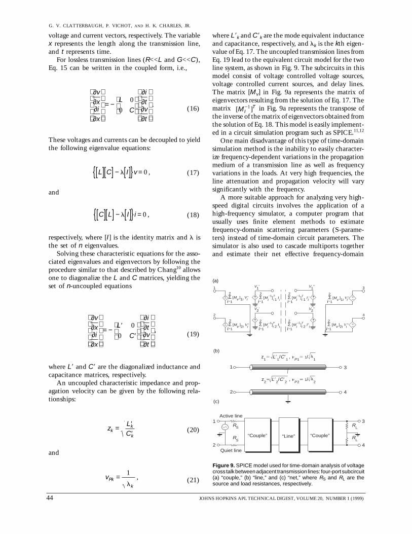
T21 in Fig. 9a represents the transpose ofthe inverse of the matrix of eigenvectors obtained fromthe solution of Eq. 18. This model is easily implement-ed in a circuit simulation program such as SPICE.11,12
One main disadvantage of this type of time-domainsimulation method is the inability to easily character-ize frequency-dependent variations in the propagationmedium of a transmission line as well as frequencyvariations in the loads. At very high frequencies, theline attenuation and propagation velocity will varysignificantly with the frequency.
A more suitable approach for analyzing very high-speed digital circuits involves the application of ahigh-frequency simulator, a computer program thatusually uses finite element methods to estimatefrequency-domain scattering parameters (S-parame-ters) instead of time-domain circuit parameters. Thesimulator is also used to cascade multiports togetherand estimate their net effective frequency-domain
Figure 9. SPICE model used for time-domain analysis of voltagecross talk between adjacent transmission lines: four-port subcircuit(a) “couple,” (b) “line,” and (c) “net,” where RS and RL are thesource and load resistances, respectively.
(a)
3
4
RL
RL
RS
RS
Z1
2
z25 L9
2/C9
2 , n
P25 1/ l
2
1 3
2 4
z15 L9
1/C9
1 , n
P15 1/ l
1
Active line
Quiet line
“Couple” “Line” “Couple”
(b)
(c)
Σ [Mv ]1i Vi′2
Σ [Mv ]2i Vi′2
Σ [MI ]i 1 Ii
2
Σ [MI ]i 2 Ii
2Σ [Mv ]2i Vi′′2
Σ [MI ]i 1 Ii′
2
i=1
Σ [MI ]i 2 I ′i
2
Σ [Mv ]1i Vi′′2
3
4
1
2
12
12
V1′ V1′′
V2′ V2′′
12
12
➝➝
➝➝
i=1
i=1i=1
i=1
i=1
i=1
i=1
–1 T –1 T
–1 T –1 T
NS HOPKINS APL TECHNICAL DIGEST, VOLUME 20, NUMBER 1 (1999)
SOME KEY ISSUES IN MICROELECTRONIC PACKAGING
S-parameters. The finite element formulation can ac-count for skin effects, dielectric losses, coupling effects,and parasitic reactances caused by discontinuity struc-tures such as transmission line bends and vias.
To obtain time-domain results, the frequency re-sponse for the complete network is computed. Theimpulse response is then calculated by performing aninverse Fourier transform on the frequency response.The time-domain waveforms transmitted through thecircuit are then computed by performing a convolutionon the circuit’s impulse response with the desired inputsignal waveform.
Analysis of Vias in Low-Temperature Co-firedCeramic MCM-Cs
This section illustrates the alternative frequency-domain approach for analyzing signal transmission inthe time domain. Our example is the investigation ofthe degradation effect that a via has on a high-speeddigital signal as it traverses through the via. The resultsfrom the via simulation presented here will subse-quently be incorporated into a larger electrical modelfor a clock distribution circuit detailed in the nextsection. This clock distribution circuit is to be used ina superconductive network switching circuit. We candefine a via as a vertical, electrically conductive pathbetween one conductor layer and another within amultilayer circuit board. By using the complex bound-ary conditions of the via, we can estimate the S-parameters of this multilevel connection and then usethe results in a frequency-domain simulator where thevia is represented as a simple two-port network. Whenvias, represented as two-port networks, are cascadedwith sections of transmission line networks for use ina frequency-domain simulator, an accurate and com-putationally efficient method for simulating high-speed signal transmission through the circuit board isachieved.
Vias are required in multilayer circuits to verticallytranslate signals between different conductor layers.As circuit elements, vias are normally modeled as smallinductors. The magnitude of this inductance is usuallyapproximated by
L = . hh
d5 08
41ln ,
+
(22)
where L is the inductance in nanohenries, h is the vialength in inches, and d is the via diameter in inches.
At very low frequencies this parasitic inductancehas no effect on the signal as it propagates betweenlayers. As the frequency content of the signal increas-es, the inductive reactance presented by this via maybecome significant.
JOHNS HOPKINS APL TECHNICAL DIGEST, VOLUME 20, NUMBER 1 (1
We considered a low-temperature, co-fired ceramictape from DuPont for a multilayer MCM substrate forhigh-speed superconducting ICs. The application is ahigh-speed (10-GHz) serial-to-parallel converter. Therise times of such devices are nominally 40 ps, with amaximum frequency content of approximately 12.5GHz. The loss tangent for the DuPont 901 materialis less than 0.002 for frequencies as high as 20 GHz.The gold conductor thickness for this fabrication pro-cess is typically 8 to 12 mm, and the surface roughnessof these conductors may range from 0.33 to 0.86 mm.The skin depth for gold at 2.5 GHz is 1.6 mm, whileat 10 GHz it is 0.79 mm. Since the skin depth is smallerthan the metallization thickness, the series resistancewill vary with frequency. For frequencies above 10GHz, the skin depth is on the order of the surfaceroughness of the conductor, and the effective seriesresistance will increase even further. For high-speeddigital signals, variations in resistance, propagationvelocity, etc., with respect to frequency lead to disper-sion and distortion of the pulse (e.g., rounding of pulseedges and spreading of pulse width).
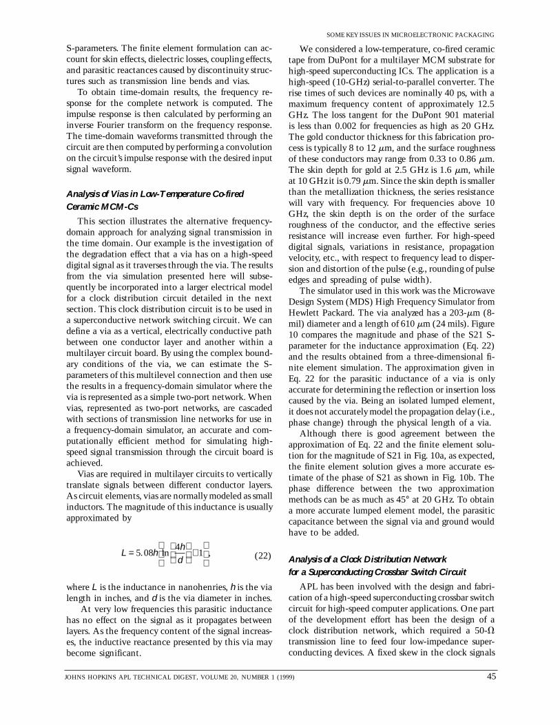
The simulator used in this work was the MicrowaveDesign System (MDS) High Frequency Simulator fromHewlett Packard. The via analyzed has a 203-mm (8-mil) diameter and a length of 610 mm (24 mils). Figure10 compares the magnitude and phase of the S21 S-parameter for the inductance approximation (Eq. 22)and the results obtained from a three-dimensional fi-nite element simulation. The approximation given inEq. 22 for the parasitic inductance of a via is onlyaccurate for determining the reflection or insertion losscaused by the via. Being an isolated lumped element,it does not accurately model the propagation delay (i.e.,phase change) through the physical length of a via.
Although there is good agreement between theapproximation of Eq. 22 and the finite element solu-tion for the magnitude of S21 in Fig. 10a, as expected,the finite element solution gives a more accurate es-timate of the phase of S21 as shown in Fig. 10b. Thephase difference between the two approximationmethods can be as much as 45° at 20 GHz. To obtaina more accurate lumped element model, the parasiticcapacitance between the signal via and ground wouldhave to be added.
Analysis of a Clock Distribution Networkfor a Superconducting Crossbar Switch Circuit
APL has been involved with the design and fabri-cation of a high-speed superconducting crossbar switchcircuit for high-speed computer applications. One partof the development effort has been the design of aclock distribution network, which required a 50-Vtransmission line to feed four low-impedance super-conducting devices. A fixed skew in the clock signals
999) 45
G. V. CLATTERBAUGH, P. VICHOT, AND H. K. CHARLES, JR.
Figure 10. Estimated S21 S-parameter magnitude (a) and phase(b) for a multilayer ceramic via using an analytical approximation(red curves) and finite element method (green curves).
23.0
22.5
22.0
21.5
21.0
20.5
0
20151050Frequency (5 GHz/division)
S21
S-p
aram
eter
(dB
)
280
260
240
220
0
20151050Frequency (5 GHz/division)
S21
ang
le (d
eg)
(a)
(b)
of 12 ps between inputs was also required. Since thevoltage level required to switch the QFP logic was anorder of magnitude lower than the input signal, thedesign would allow for one reflection back to thesource, which then must absorb all of the reflectedenergy. Multiple reflections could not be tolerated, asthey would compromise signal integrity at the QFPinputs and could affect the skew.
Since the signal was a fast-rising digital pulse, anarrowband impedance transformer was not accept-able. Resistor-based transformers are normally wide-band, but the heat dissipation of the resistors wouldraise the temperature of the superconducting ICsabove the superconducting temperature.
After some preliminary design evaluations, a spiderclock circuit was designed that featured a 50-V lineterminating directly into four 26-V legs. In the spiderdesign, a single impedance mismatch exists at thepoint where the 50-V input line transitions into thefour 26-V lines. Provided that the circuit is impedance
46 JOH
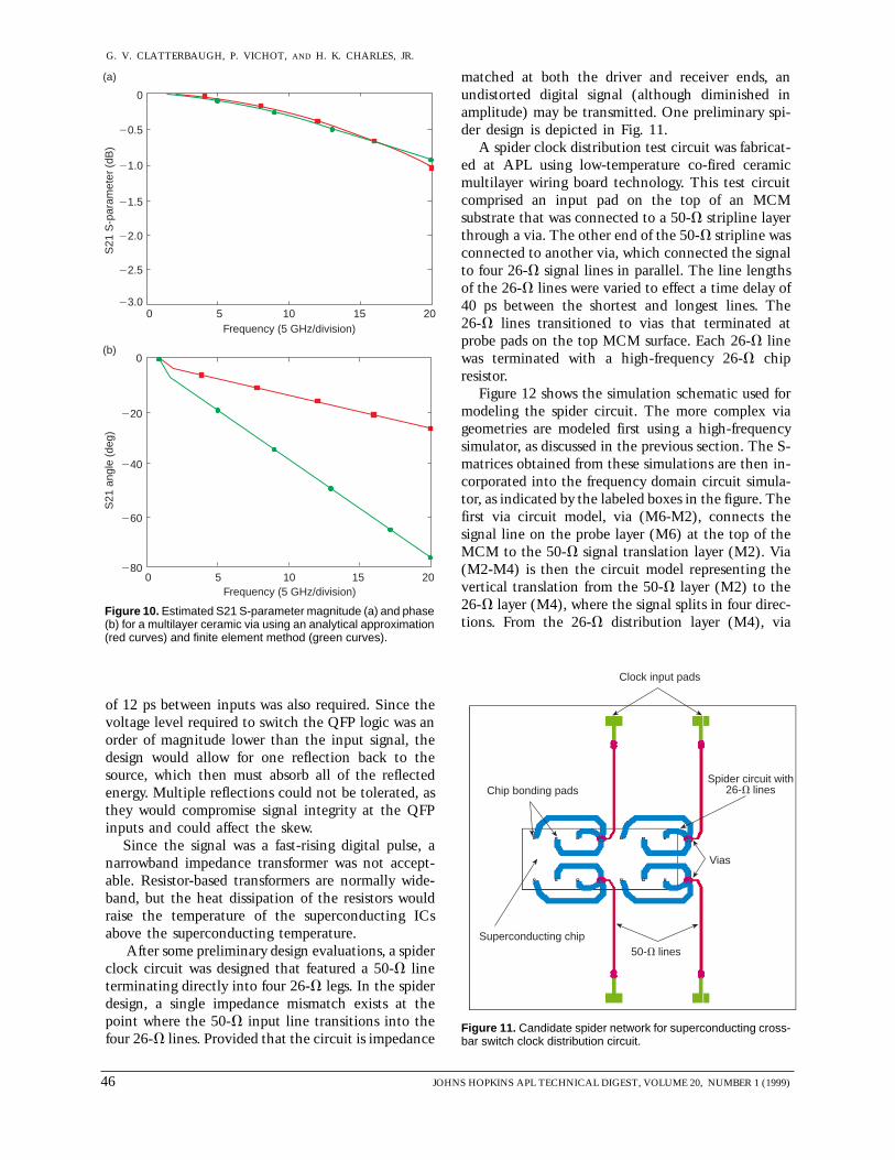
matched at both the driver and receiver ends, anundistorted digital signal (although diminished inamplitude) may be transmitted. One preliminary spi-der design is depicted in Fig. 11.
A spider clock distribution test circuit was fabricat-ed at APL using low-temperature co-fired ceramicmultilayer wiring board technology. This test circuitcomprised an input pad on the top of an MCMsubstrate that was connected to a 50-V stripline layerthrough a via. The other end of the 50-V stripline wasconnected to another via, which connected the signalto four 26-V signal lines in parallel. The line lengthsof the 26-V lines were varied to effect a time delay of40 ps between the shortest and longest lines. The26-V lines transitioned to vias that terminated atprobe pads on the top MCM surface. Each 26-V linewas terminated with a high-frequency 26-V chipresistor.
Figure 12 shows the simulation schematic used formodeling the spider circuit. The more complex viageometries are modeled first using a high-frequencysimulator, as discussed in the previous section. The S-matrices obtained from these simulations are then in-corporated into the frequency domain circuit simula-tor, as indicated by the labeled boxes in the figure. Thefirst via circuit model, via (M6-M2), connects thesignal line on the probe layer (M6) at the top of theMCM to the 50-V signal translation layer (M2). Via(M2-M4) is then the circuit model representing thevertical translation from the 50-V layer (M2) to the26-V layer (M4), where the signal splits in four direc-tions. From the 26-V distribution layer (M4), via
Figure 11. Candidate spider network for superconducting cross-bar switch clock distribution circuit.
Chip bonding pads
Superconducting chip50-V lines
Vias
Spider circuit with26-V lines
Clock input pads
NS HOPKINS APL TECHNICAL DIGEST, VOLUME 20, NUMBER 1 (1999)
SOME KEY ISSUES IN MICROELECTRONIC PACKAGING
Figure 12. Circuit representation of a spider clock distribution network. (Z0 = impedence, RS = source impedence, td = propagation delay,and tr = rise time; tr = 20 ps and unit-step source = 0 to 2 V.)
(M4-M6) represents the vertical translation back tothe uppermost layer (M6) of the MCM, where theoutput signals are probed across the 26-V chip resis-tance. The transmission line models in Fig. 12 char-acterize the horizontal propagation of the signals onthe individual layers of the MCM. The excitation isa unit-step voltage source with a rise time of 20 ps.
Figure 13a shows the computed waveforms from thecircuit simulation for a unit-step voltage source witha 10 to 90% rise time of 20 ps. These waveformsrepresent the signals transmitted to each of the fouroutputs of the spider circuit. Line A represents theshortest leg of the circuit with an equivalent propaga-tion delay of 11 ps; line D represents the longest legwith a delay of 51 ps (see Fig. 12). The waveform forline A has a rise time of 38 ps; the waveform for lineD has a rise time of 47 ps. The slower edge rate of lineD may be attributed to transmission line attenuationsince its path length is nearly 5 times greater than lineA’s. Figure 13b shows the effects of disparate signaledge rates on the overall skew of the circuit. Thecircuit was originally designed to have a time delay of40 ps between the transmitted signals on line A andline D. Accounting for the unequal edge rates betweenlines A and D, the actual time delay measuredis 44 ps.
SUMMARY
The relentless progression of IC manufacturers to-ward the fabrication of circuits with higher speeds andhigher densities is constantly challenging the abilityof packaging engineers to integrate ICs into highly
JOHNS HOPKINS APL TECHNICAL DIGEST, VOLUME 20, NUMBER 1 (
functional, high-performance electronic systems. Thisarticle has discussed some of the methods developedto assist the electronic packaging engineer in findingsolutions to the difficult problems associated with suchhigh-performance electronics.
Some of the issues pertaining to the wireability ofdensely populated wiring boards and high I/O areaarray–style packages have been addressed and exam-ples have been given. The message here is that higherdensity packages and devices will require designguidelines with smaller features such as lines, spaces,and vias.
Issues pertaining to manufacturing cost modelingwere also presented. The KGD problem was examinedin some detail. Several yield models were discussed andindustry data provided that lend some insight into theproblem. A cost model was described that showed howassembly cost may depend as much on repair and testcosts as it does on the probability that a chip is a KGD.Cost comparisons were made among two prominenttechnologies, MCM-L and SMT, and a third more re-cent player, CSP. Cost analyses indicated that in smallerquantities, MCM-L would remain the least expensivelaminate-based packaging technology, whereas in high-er quantities, CSP was more cost-effective.
The difficult issue of thermally analyzing complexPWB laminates was presented, and methods for moreaccurately predicting device temperatures were provid-ed. Finally, methods for analyzing signal integrity in amulticonductor environment were discussed. Severalexamples illustrating the use of these methods to solvecurrent high-speed electronic packaging design prob-lems were also given.
1999) 47
G. V. CLATTERBAUGH, P. VICHOT, AND H. K. CHARLES, JR.
Figure 13. Simulated circuit performance for a spider clock distribution circuit. (a) Waveforms at 26-V loads for the four legs of the spiderclock distribution circuit in response to a unit-step voltage with a 20-ps rise time. (b) Estimated signal skew between the shortest andlongest legs.
0.35
–0.15
–0.05
0.05
0.15
0.25
100 200 300 400 500Time (ps)
Sig
nal m
agni
tude
(V
)
Line BLine A
Line C
Line D
(a)
0.35
–0.15
–0.05
0.05
0.15
0.25
Sig
nal m
agni
tude
(V
)
100 200 300 400Time (ps)
44 psLine A
Line D
(b)
REFERENCES1Rose, K., Chiba, T., Heller, W. R., and Mikhail, W. F., “Package Wiring and
Terminals,” in Microelectronics Packaging Handbook, Part I, R. R. Tummala,E. J. Rymaszewski, and A. G. Klopfstein (eds.), Chapman & Hall, New York,pp. 130–195 (1997).
2Rickerts, R. G., “Design Tradeoffs,” in Electronic Materials Handbook, Vol. 1,Packaging, ASM International, Materials Park, OH, pp. 18–44 (1989).
3Schmidt, D. C., “Circuit Pack Parameter Estimation Using Rent’s Rule,”IEEE Trans. Comput. CAD-1(4), 186–192 (Oct 1982).
4Amerson, R., and Kuekes, P., “A Twenty-Seven Chip MCM-C,” in SPIEProc. 2256, pp. 578–582 (1994).
5Rozel, L., “MCM Testing,” Electronic Engineering Times (9 Oct 1995).6Charles, Jr., H. K., “Cost Versus Technology Trade-Offs for Multichip
Modules,” ISHM J. Microelectron. Electron. Packaging 19(3), 295–300 (1996).7Messner, G., “Cost-Density Analysis of Interconnections,” IEEE Trans.
11Tripathi, V. K., and Retting, J. B., “A SPICE Model for Multiple CoupledMicrostrips and Other Transmission Lines,” IEEE Trans. Microwave TheoryTech. MTT-33, 1513–1518 (Dec 1985).
12Clatterbaugh, G. V., and Charles, Jr., H. K., Advanced Packaging for VLSI/VHSIC Applications: Electrical, Thermal, and Mechanical Considerations - AnIR&D Report, TG-1362, JHU/APL, Laurel, MD (Nov 1987).
THE AUTHORS
GUY V. CLATTERBAUGH received B.S. and M.S. degrees in physics fromDrexel University. He has been a staff scientist with the Microelectronics Groupand then the Electronic Services Group at APL since 1982. Mr. Clatterbaughwas appointed to the Principal Professional Staff in 1996. He has authored orco-authored over 60 papers concerning wire bonding, soldering, high-speeddigital packaging, and multichip modules. Mr. Clatterbaugh’s current interestsinclude electro-optical interconnections, flip-chip bonding, and surface-mountsoldering. He is currently a member of the International Microelectronics andPackaging Society. His e-mail address is [email protected].
HARRY K. CHARLES, JR., received his B.S. in 1967 from Drexel Universityand his Ph.D. in 1972 from The Johns Hopkins University, both in electricalengineering. He joined APL in 1972 as a Postdoctoral Research Associate. Heis currently Assistant Department Head for Engineering in the TechnicalServices Department and a member of the Principal Professional Staff. Dr.Charles has worked for 25 years in the microelectronics arena and is a specialistin electronic devices, systems, packaging, and reliability. His latest interestsinclude multichip module design, fabrication, and testing; advanced intercon-nect; biomedical instrumentation; and novel sensors based on MEMS technol-ogy. He is a Fellow and former President of IMAPS (The InternationalMicroelectronics and Packaging Society), a Fellow of the IEEE, and a memberof the Board of Governors of IEEE’s Components Packaging and ManufacturingTechnology (CPMT) Society. His e-mail address is [email protected].
PAUL VICHOT received his B.S. degree in physics from Duke University in1993 and an M.S. degree in electrical engineering from the University ofColorado at Boulder in 1997. He is currently working towards a Ph.D. inelectrical engineering at the University of Colorado. Mr. Vichot recently joinedAPL’s Strike Warfare Systems Group, where he has been working on thedevelopment of high-performance digital systems based on superconductingdevice technology. His current research interests include electronic packag-ing, microwaves, superconductivity, and digital systems. His e-mail address [email protected].