Page 1
1
SERVICE MANUAL FE-2 CHASSISMODEL COMMANDER DEST CHASSIS NO.
KV-21FX30B RM-887 FR SCC-Q54G-A
KV-21FX30E RM-887 ESP SCC-Q53H-A
MODEL COMMANDER DEST CHASSIS NO.
RM-889
KV-21FX30K RM-887 OIRT SCC-Q51J-A
Page 2
2
TABLE OF CONTENTS
Section Title Page Section Title Page
Specifications .................... 3Connectors .................... 4Self Diagnostic Software .................... 5
1. GENERALSwitching On the TV andAutomatically Tuning .................... 6Introducing the Menu System .................... 7Menu Guide .................... 7Teletext .................... 10Specifications .................... 11Troubleshooting .................... 11
2. DISASSEMBLY
2-1. Rear Cover Removal .................... 122-2. Speaker Disconnection .................... 122-3. Speaker Box Removal .................... 122-4. Speaker Box Disassembly .................... 122-5. A Board PWB Removal 1 .................... 132-6. A Board PWB Removal 2 .................... 132-7. Service Position .................... 132-8. Wire Dressing .................... 132-9. Picture Tube Removal .................... 14
3. SET-UP ADJUSTMENTS
3-1. Beam Landing .................... 153-2. Convergence .................... 163-3. Focus Adjustment .................... 183-4. Screen (G2), White Balance .................... 18
4. CIRCUIT ADJUSTMENTS
4-1. Electrical Adjustments .................... 194-2. Test Mode 1 .................... 214-3. Test Mode 2 .................... 21
5. DIAGRAMS
5-1. Block Diagrams (1) .................... 23Block Diagrams (2) .................... 25
5-2. Circuit Board Location .................... 265-3. Schematic Diagrams and
Printed Wiring Boards .................... 26* C Board .................... 27* A Board .................... 29
5-4. Semiconductors .................... 375-5. IC Blocks .................... 39
6. EXPLODED VIEWS
6-1. Chassis .................... 406-2. Picture Tube .................... 41
7. ELECTRICAL PARTS LIST .................... 42
CAUTION
SHORT CIRCUIT THE ANODE OF THE PICTURE TUBE AND THEANODE CAP TO THE METAL CHASSIS, CRT SHIELD, OR THECARBON PAINTED ON THE CRT, AFTER REMOVAL OF THEANODE CAP.
WARNING !!
AN ISOLATION TRANSFORMER SHOULD BE USED DURINGANY SERVICE WORK TO AVOID POSSIBLE SHOCK HAZARDDUE TO LIVE CHASSIS, THE CHASSIS OF THIS RECEIVER ISDIRECTLY CONNECTED TO THE POWER LINE.
SAFETY-RELATED COMPONENT WARNING !!
COMPONENTS IDENTIFIED BY SHADING AND MARKED £ ONTHE SCHEMATIC DIAGRAMS, EXPLODED VIEWS AND IN THEPARTS LIST ARE CRITICAL FOR SAFE OPERATION. REPLACETHESE COMPONENTS WITH SONY PARTS WHOSE PARTNUMBERS APPEAR AS SHOWN IN THIS MANUAL OR INSUPPLEMENTS PUBLISHED BY SONY.
ATTENTION
APRES AVOIR DECONNECTE LE CAP DE’LANODE,COURT-CIRCUITER L’ANODE DU TUBE CATHODIQUE ETCELUI DE L’ANODE DU CAP AU CHASSIS METALLIQUE DEL’APPAREIL, OU AU COUCHE DE CARBONE PEINTE SUR LETUBE CATHODIQUE OU AU BLINDAGE DU TUBECATHODIQUE.
ATTENTION !!
AFIN D’EVITER TOUT RISQUE D’ELECTROCUTIONPROVENANT D’UN CHÁSSIS SOUS TENTION, UNTRANSFORMATEUR D’ISOLEMENT DOIT ETRE UTILISÈ LORSDE TOUT DÈPANNAGE LE CHÁSSIS DE CE RÈCEPTEUR ESTDIRECTMENT RACCORDÈ Á L’ALIMENTATION SECTEUR.
ATTENTION AUX COMPOSANTS RELATIFS ÁLA SECURITÈ!!
LES COMPOSANTS IDENTIFIÈS PAR UNE TRAME ET PAR UNEMARQUE £ SUR LES SCHÈMAS DE PRINCIPE, LES VUESEXPLOSÈES ET LES LISTES DE PIECES SONT D’UNE IMPOR-TANCE CRITIQUE POUR LA SÈCURITÈ DU FONCTIONNEMENT,NE LES REMPLACER QUE PAR DES COMPSANTS SONY DONTLE NUMÈRO DE PIÈCE EST INDIQUÈ DANS LE PRÈSENTMANUEL OU DANS DES SUPPLÈMENTS PUBLIÈS PAR SONY.
Page 3
3
LEDOMMETI metsySnoisiveleT metsySoeretS egarevoClennahC metsySroloC
B L,I,K/D,H/G/BMACIN/NAMREG
oeretS
01F-2F,21E-2E:FHV96B-12B,96F-12F,96E-12E:FHUQ-B,02S-1S,30S-10S:VTELBAC
14S-12S:REPYH
MACES,LAP85.3CSTN,34.4CSTN
)NIOEDIV(
E K/D,H/G/BMACIN/NAMREG
oeretS
21E-2E:FHV96E-12E:FHU
02S-1S,30S-10S:VTELBAC14S-12S:REPYH
MACES,LAP85.3CSTN,34.4CSTN
)NIOEDIV(
K K/D,H/G/BMACIN/NAMREG
oeretS
21R-10R,21E-2E:FHV96R-12R,96E-12E:FHU
02S-1S,30S-10S:VTELBAC14S-12S:REPYH
MACES,LAP85.3CSTN,34.4CSTN
)NIOEDIV(
emaNledoMmetI
B03XF12-VK E03XF12-VK K03XF12-VK
bmoClaP FFO FFO FFO
PIP FFO FFO FFO
ytiroirPBGR NO NO NO
xoBrefooW FFO FFO FFO
1tracS NO NO NO
2tracS NO NO NO
)3(nitnorF NO NO NO
4tracS FFO FFO FFO
rotcejorP FFO FFO FFO
G/BmroN NO NO NO
ImroN NO FFO FFO
K/DmroN NO NO NO
SUAmroN FFO FFO FFO
LmroN NO FFO FFO
TASmroN FFO FFO FFO
MmroN FFO FFO FFO
txeteleT NO NO NO
oeretSmaciN NO NO NO
ebuTerutciP
nortinirTDFyalpsiDtalF)sehcni12(mc55xorppA
derusaemerutcipmc15xorppA()yllanogaid
tuptuodnuoSrekaepstfeLdnathgiR )SMR(W7x2)rewoPcisuM(W41x2
snoitacificepSlareneG
]RAER[slanimreTtuptuO/tupnIstnemeriuqeRrewoP V042-022
rotcennocoruEnip-12:1)dradnatsCELENEC(
.slangisoediVdnaoiduArofstupnI.BGRrofstupnI
oiduAdnaoediVVTfostuptuO.slangis
noitpmusnoCrewoP W78
rotcennocoruEnip-12:2.slangisoediVdnaoiduArofstupnI
.oediVSrofstupnI.slangisoiduAdnaoediVVTfostuptuO
)elbatceles(
snoisnemiD mm584x644x545xorppA
thgieW gk62xorppA
srotcennoCACR slangisoiduaroftuptuOelbairaV seirosseccAdeilppuS)1(rednammoCetomeR788-MR
)2(yrettab6RdetangisedCEI
]TNORF[slanimreTtuptuO/tupnI serutaeFrehtOtxeteleT,noitcetedotuAmetsysVT
kniltramS
kcajenohpdaeH kcajinimoerets lortnoCderarfnI:metsySlortnoCetomeR
stupnioiduA skcajonohpstnemeriuqerrewoP
cdV3noitangisedCEIseirettab2
)AAezis(6RstupnioediV skcajonohp
.ecitontuohtiwegnahcottcejbuserasnoitacificepsdnangiseD
Page 4
4
21 pin connector
Connected Not Connected (open) * at 20Hz - 20kHz
Pin No 1 2 4 Signal Signal level
1 Audio output B(right)
Standard level : 0.5V rmsOutput impedence : Less than 1kohm*
2Audio output B(right)
Standard level : 0.5V rmsOutput impedence : More than 10kohm*
3Audio output A(left)
Standard level : 0.5V rmsOutput impedence : Less than 1kohm*
4 Ground (audio)
5 Ground (blue)
6 Audio input A(left)
Standard level : 0.5V rmsOutput impedence : More than 10kohm*
7 Blue input 0.7 +/- 3dB, 75 ohms positive
8 Function select(AV control)
High state (9.5-12V) : Part mode Low state (0-2V) : TV modeInput impedence : More than 10K ohmsInput capacitance : Less than 2nF
9 Ground (green)
10 Open
11 Green Green signal : 0.7 +/- 3dB, 75 ohms, positive
12 Open
13 Ground (red)
14 Ground (blanking)
15
_ _ Red input 0.7 +/- 3dB, 75 ohms, positive
_ (S signal Chroma input)
0.3 +/- 3dB, 75 ohms, positive
16 Blanking input(Ys signal)
High state (1-3V) Low state (0-0.4V)Input impedence : 75 ohms
17 Ground (video output)
18 Ground (video input)
19 Video output 1V +/- 3dB, 75ohms, positive sync 0.3V(-3+10dB)
20
_ _ Video input 1V +/- 3dB, 75ohms, positive sync 0.3V(-3+10dB)
_ Video inputY (S signal)
1V +/- 3dB, 75ohms, positive sync 0.3V(-3+10dB)
21 Common ground(plug, shield)
19
17
15
13
11
9
7
5
3
1
20
18
16
14
12
10
8
6
4
2
21
Rear Connection Panel Front Connection Panel
Page 5
5
FE-2 SELF DIAGNOSTIC SOFTWARE
The identification of errors within the FE-2 chassis is triggered in one of two ways :- 1: Busy or 2: Device failure to respond to IIC. In the eventof one of these situations arising the software will first try to release the bus if busy (Failure to do so will report with a continuous flashingLED) and then communicate with each device in turn to establish if a device is faulty. If a device is found to be faulty the relevant device numberwill be displayed through the LED (Series of flashes which must be counted) See table 1., non fatal errors are reported using this method.Each time the software detects an error it is stored within the NVM. See Table 2.
Flash Timing Example : e.g. error number 3
StBy LED
ON ON ON
OFF OFF
Table 1 How to enter into Table 2
1. Turn on the main power switch of the TV set and enter intothe‘Stanby Mode’.
2. Press the following sequence of buttons on the RemoteCommander.
i+ 5 -(ON SCREEN (DIGIT 5) (VOLUME -) (TV) DISPLAY)
3. The following table will be displayed indicating the errorcount.
Table 2
Note: To clear the error count data press ‘80’ on the Remote commander.
UNEMRORRE
20E30E40E50E60E70E80E90E01E11E
EMITGNIKROWSRUOH
SETUNIM
PCOA/NPVO
CNYSVRKI
CIIMVN
ELGNUJRENUT
PDNUOSV8
)552,0()552,0()552,0()552,0()552,0()552,0()552,0()552,0()552,0()552,0(
0000000000
211
egasseMrorrEDELedoC
rorreoN 00devreseR 10
)noitcetorPtnerruCrevO(PCO 20desUtoN 30
cnySlacitreVoN 40norewoptarorrERKI 50
norewoptawolsenilatadro/dnakcolcsubCII 60norewoptaegdelwonkcasubCIIonMVN 70
desUtoN 80norewoptaegdelwonkcaonrenuT 90
rorrErossecorPdnuoS 01rorrestlov8rellortnocelgnuJ 11
Page 6
6
8Fi
rst
Tim
e O
per
atio
n
You
r T
V is
now
rea
dy fo
r us
e
5T
he A
uto
Tun
ing
men
u ap
pear
s on
the
scre
en. P
ress
the
O
K b
utto
n to
sel
ect Y
es.
6T
he T
V s
tart
s to
aut
omat
ical
ly s
earc
h an
d s
tore
all
av
aila
ble
broa
dca
st c
hann
els
for
you.
Thi
s pr
oced
ure
coul
d ta
ke s
ome
min
utes
. Ple
ase
be
pat
ient
and
do
not p
ress
any
but
ton.
Oth
erw
ise
the
a
utom
atic
tuni
ng w
ill n
ot b
e co
mpl
eted
.
If n
o ch
anne
ls w
ere
foun
d d
urin
g th
e au
to tu
ning
pr
oces
s th
en a
new
men
u ap
pear
s au
tom
atic
ally
on
the
scre
en a
skin
g yo
u to
con
nect
the
aeri
al. P
leas
e co
nnec
t the
aer
ial (
see
page
6) a
nd p
ress
OK
. The
au
to tu
ning
pro
cess
will
sta
rt a
gain
.
7A
fter
all
avai
labl
e ch
anne
ls a
re c
apti
oned
and
sto
red
,
the
Pro
gram
me
Sor
tin
g m
enu
appe
ars
auto
mat
ical
ly
on th
e sc
reen
ena
blin
g yo
u to
cha
nge
the
ord
er in
w
hich
the
chan
nels
app
ear
on th
e sc
reen
.
a)If
you
wis
h to
kee
p th
e br
oad
cast
cha
nnel
s in
the
tu
nned
ord
er, g
o to
ste
p 8.
b)
If y
ou w
ish
to s
tore
the
chan
nels
in a
dif
fere
nt o
rder
:
1Pr
ess
the
orbu
tton
to s
elec
t the
pro
gram
me
num
ber
wit
h th
e ch
anne
l (T
V B
road
cast
) you
wis
h
to r
earr
ange
, the
n pr
ess
the
butt
on.
2Pr
ess
the
orbu
tton
to s
elec
t the
new
prog
ram
me
num
ber
posi
tion
for
your
sel
ecte
d
chan
nel (
TV
Bro
adca
st),
then
pre
ss
.
3R
epea
t ste
ps b
)1 a
nd b
)2 if
you
wis
h to
cha
nge
the
ord
er o
f the
oth
er c
hann
els.
8Pr
ess
the
ME
NU
but
ton
to r
emov
e th
e m
enu
from
the
sc
reen
.
No
chan
nel f
ound
Ple
ase
conn
ect a
eria
l
Con
firm
OK
Pro
gram
me:
01
Sys
tem
:
B/G
Cha
nnel
:
C
21
Aut
o Tu
ning
Sea
rchi
ng...
Pro
gram
me
Sor
ting
Sel
ect c
hann
el:
Exi
t:
ME
NU
Pro
gram
me:
01
T
VE
02
T
VE
2
03
TV
3
04
C33
05
C
27
06
C
58
OK
Pro
gram
me
Sor
ting
Sel
ect n
ew p
ositi
on:
Exi
t:
ME
NU
Pro
gram
me:
01
T
VE
02
T
VE
2
03
TV
3
04
C33
05
C
27
06
C
58
05
C
27
OK
K K K
Do
you
wan
t to
star
t au
tom
atic
tuni
ng?
Yes
No
OK
K
ME
NU
7
GB
Lang
uage
Sel
ect L
angu
age:
i4 Sve
nska
Nor
skE
nglis
hN
eder
land
sFr
ança
isIta
liano
i$
OK
Cou
ntry
Sel
ect c
ount
ry:
i4 Sve
rige
Nor
ge- Ita
liaD
euts
chla
ndÖ
ster
reic
h i$
OK
K K K
If pi
ctur
e sl
ants
, ple
ase
adju
st p
ictu
re r
otat
ion
Not
nec
essa
ryA
djus
t now
OK
Sw
itch
ing
On
th
e T
V a
nd
Au
tom
ati
call
y T
un
ing
The
firs
t tim
e yo
u sw
itch
on
your
TV
, a s
eque
nce
of m
enu
scre
en a
ppea
r on
the
TV
ena
blin
g yo
u to
: 1) c
hoos
e th
e la
ngua
ge o
f the
men
u sc
reen
, 2) c
hoos
e th
e co
untr
y in
whi
ch y
ou w
ish
to o
pera
te th
e T
V, 3
) ad
just
the
pict
ure
slan
t 4) s
earc
h an
d s
tore
all
avai
labl
e ch
anne
ls (T
V
Bro
adca
st) a
nd 5
) cha
nge
the
ord
er in
whi
ch th
e ch
anne
ls (T
V B
road
cast
) app
ear
on th
e sc
reen
.H
owev
er, i
f you
nee
d to
cha
nge
any
of th
ese
sett
ings
, you
can
do
that
by
sele
ctin
g th
e ap
prop
riat
e op
tion
in th
e (S
et U
p m
enu)
or
by p
ress
ing
the
Aut
o St
art U
p B
utto
n
on th
e T
V s
et.
Firs
t Ti
me
Op
erat
ion
cont
inue
d...
1C
onne
ct th
e T
V p
lug
to th
e m
ains
soc
ket (
220-
240V
AC
, 50
Hz)
Pres
s th
e o
n/of
f but
ton
on th
e T
V s
et to
turn
on
the
TV
.T
he fi
rst t
ime
you
pres
s th
is b
utto
n, a
Lan
guag
e m
enu
dis
play
s au
tom
atic
ally
on
the
TV
scr
een.
2Pr
ess
the
orbu
tton
on
the
rem
ote
cont
rol t
o se
lect
th
e la
ngua
ge, t
hen
pres
s th
e O
K b
utto
n to
con
firm
you
r se
lect
ion.
Fro
m n
ow o
n al
l the
men
us w
ill a
ppea
r in
the
sele
cted
lang
uage
.
3T
he C
oun
try
men
u ap
pear
s au
tom
atic
ally
on
the
TV
sc
reen
. Pre
ss th
e or
butt
on to
sel
ect t
he c
ount
ry in
w
hich
you
will
ope
rate
the
TV
set
, the
n pr
ess
the
OK
bu
tton
to c
onfi
rm y
our
sele
ctio
n.
• If
the
coun
try
in w
hich
you
wan
t to
use
the
TV
set
doe
s no
t app
ear
in th
e lis
t, se
lect
“-”
inst
ead
of a
co
untr
y.•
In o
rder
to a
void
wro
ng te
lete
xt c
hara
cter
s fo
r C
yrill
ic la
ngua
ges
we
reco
mm
end
to s
elec
t Rus
sia
coun
try
in th
e ca
se th
at y
our o
wn
coun
try
doe
s not
ap
pear
in th
e lis
t.
4B
ecau
se o
f the
ear
th’s
mag
neti
sm, t
he p
ictu
re m
ight
sla
nt.
The
Pic
ture
Rot
atio
n
men
u al
low
s yo
u to
cor
rect
the
pict
ure
slan
ts if
it is
nec
essa
ry.
a) I
f it i
s no
t nec
essa
ry, p
ress
orto
sel
ect N
ot
nec
essa
ry a
nd p
ress
OK
.
b) I
f it i
s ne
cess
ary,
pre
ssor
to s
elec
t Ad
just
now
, th
en p
ress
OK
and
cor
rect
any
sla
nt o
f the
pic
ture
be
twee
n –5
and
+5
by p
ress
ing
or. F
inal
ly p
ress
OK
to s
tore
.
The
ope
ratin
g in
stru
ctio
ns m
entio
ned
here
are
par
tial a
bstr
acts
fro
m t
he ‘O
pera
ting
Inst
ruct
ion
Man
ual’.
The
pag
e nu
mbe
rs o
f th
e ‘O
pera
ting
Inst
ruct
ion
Man
ual’
rem
ain
as in
the
man
ual.
SECTION 1 GENERAL
Page 7
7
9
GB
Intr
od
uci
ng
an
d U
sin
g t
he M
en
u S
yst
em
You
r T
V u
ses
an o
n-sc
reen
men
u sy
stem
to g
uid
e yo
u th
roug
h th
e op
erat
ions
. Use
the
follo
win
g bu
tton
s on
the
Rem
ote
Con
trol
to o
pera
te th
e m
enu
syst
em:
1Pr
ess
the
ME
NU
but
ton
to s
wit
ch th
e fi
rst l
evel
men
u on
.
Men
u S
yste
m
2•
To
high
light
the
des
ired
men
u or
opt
ion,
pre
ssor
.•
To
ente
r to
the
sele
cted
men
u or
opt
ion,
pre
ss.
• T
o re
turn
to th
e la
st m
enu
or o
ptio
n, p
ress
.•
To
alte
r se
ttin
gs o
f you
r se
lect
ed o
ptio
n, p
ress
/
/or
.
• T
o co
nfir
m a
nd s
tore
you
r se
lect
ion,
pre
ss O
K.
3Pr
ess
the
ME
NU
but
ton
to r
emov
e th
e m
enu
from
the
scre
en.
cont
inue
d...
Men
u G
uid
e
PIC
TUR
E A
DJU
STM
ENT
The
“Pi
ctur
e A
dju
stm
ent”
men
u al
low
s yo
u to
al
ter
the
pict
ure
adju
stm
ents
.
To
do
this
: aft
er s
elec
ting
the
item
you
wan
t to
alte
r pre
ss, t
hen
pres
s re
peat
edly
//
orto
ad
just
it a
nd fi
nally
pre
ss O
K to
st
ore
the
new
ad
just
men
t.T
his
men
u al
so a
llow
s yo
u to
cus
tom
ise
the
pict
ure
mod
e ba
sed
on
the
prog
ram
me
you
are
wat
chin
g: P
erso
nal
(for
ind
ivid
ual s
etti
ngs)
. L
ive
(for
live
bro
adca
st p
rogr
amm
es).
Mo
vie
(for
film
s).
Leve
l 1
Leve
l 2
Leve
l 3 /
Fu
nct
ion
Pic
ture
Adj
ustm
ent
Mod
e: P
erso
nal
C
ontr
ast
B
right
ness
C
olou
r
Sha
rpne
ss
Hue
R
eset
OK
Pic
ture
Adj
ustm
ent
Mod
e: P
erso
nal
C
ontr
ast
B
right
ness
C
olou
r
Sha
rpne
ss
Hue
R
eset
OK
•B
righ
tnes
s, C
olou
r an
d Sh
arpn
ess
can
only
be
alte
rate
d if
“Per
sona
l” m
ode
is s
elec
ted.
•H
ue is
onl
y av
aila
ble
for
NT
SC c
olou
r si
gnal
(e.g
: USA
vid
eo ta
pes)
.•
Sele
ct R
eset
and
pre
ss O
K to
res
et th
e pi
ctur
e to
the
fact
ory
pres
et le
vels
.
ME
NU
K
ME
NU
10M
enu
Sys
tem
SOU
ND
AD
JUST
MEN
TT
he “
Soun
d A
dju
stm
ent”
men
u al
low
s yo
u to
al
ter
the
soun
d a
dju
stm
ents
.
To
do
this
: aft
er s
elec
ting
the
item
you
wan
t to
alte
r, p
ress
. t
hen
pres
s re
peat
edly
/
/ o
r to
ad
just
it a
nd fi
nally
pre
ss O
K
to s
tore
the
new
ad
just
men
t.
Leve
l 1
Leve
l 2
Leve
l 3 /
Fu
nct
ion
Thi
s m
enu
also
con
tain
s tw
o su
bmen
us a
s fo
llow
ing:
Mod
e
Per
son
al (f
or in
div
idua
l set
ting
s)
Roc
k P
op J
azz
Det
ail A
dju
stm
ent
Sou
nd
Eff
ect:
Off
:N
orm
al.
Sp
atia
l:A
cous
tic
soun
d e
ffec
t.
Au
to v
olu
me:
Off
:V
olum
e ch
anne
l cha
nges
acc
ord
ing
to
the
broa
dca
st s
igna
l.O
n:
Vol
ume
leve
l of t
he c
hann
els
will
st
ay th
e sa
me,
ind
epen
den
t of t
he
broa
dca
st s
igna
l (e.
g. in
the
case
of
adve
rtis
emen
ts).
TV
Sp
eak
ers:
Off
:So
und
from
ext
erna
l am
plif
ier
co
nnec
ted
to th
e au
dio
out
puts
on
th
e re
ar o
f the
TV
set
.O
n:
Soun
d fr
om th
e T
V s
et.
•T
rebl
e an
d B
ass
can
only
be
alte
red
if “P
erso
nal”
mod
e is
sel
ecte
d.
•Se
lect
Res
et a
nd p
ress
OK
to r
eset
the
soun
d to
the
fact
ory
pres
et le
vels
.
•In
cas
e of
a b
iling
ual b
road
cast
sel
ect D
ual S
ound
and
set
A fo
r so
und
chan
nel 1
, B fo
r so
und
chan
nel
2 or
Mon
o fo
r m
ono
chan
nel i
f ava
ilabl
e. F
or a
ste
reo
broa
dcas
t you
can
cho
ose
Ster
eo o
r M
ono.
cont
inue
d...
Pic
ture
Adj
ustm
ent
Mod
e: P
erso
nal
C
ontr
ast
B
right
ness
C
olou
r
Sha
rpne
ss
Hue
R
eset
OK
Sou
nd A
djus
tmen
tM
ode:
P
erso
nal
Tre
ble
Bas
s B
alan
ce R
eset
Dua
l Sou
nd:
M
ono
Det
ail A
djus
tmen
t
OK
Sou
nd A
djus
tmen
tM
ode:
P
erso
nal
Tre
ble
Bas
s B
alan
ce R
eset
Dua
l Sou
nd:
M
ono
Det
ail A
djus
tmen
t
OK
Page 8
8
11
GB
Men
u S
yste
m
SLEE
P TI
MER
The
“Sl
eep
Tim
er”
opti
on in
the
“Tim
er”
men
u al
low
s yo
u to
sel
ect a
tim
e pe
riod
for
the
TV
to
swit
ch it
self
aut
omat
ical
ly in
to th
e st
and
by
mod
e.
To
do
this
: aft
er s
elec
ting
the
opti
on p
ress
, th
en p
ress
orto
set t
he ti
me
peri
od d
elay
(m
ax. o
f 4 h
ours
) and
fina
lly p
ress
OK
to s
tore
. •
Whi
le w
atch
ing
the
TV
, you
can
pre
ss th
e
butt
on o
n th
e re
mot
e co
ntro
l to
disp
lay
the
ti
me
rem
aini
ng.
•O
ne m
inut
e be
fore
the
TV
sw
itch
es it
self
into
st
andb
y m
ode,
the
tim
e re
mai
ning
is d
ispl
ayed
on
th
e T
V s
cree
n au
tom
atic
ally
.
ON
TIM
ERT
he “
On
Tim
er”
opti
on in
the
“Tim
er”
men
u al
low
s yo
u to
sel
ect a
tim
e pe
riod
for
the
TV
to
swit
ch it
self
aut
omat
ical
ly o
n fr
om s
tand
by
mod
e.
To
do
this
: aft
er s
elec
ting
the
opti
on p
ress
,
then
pre
ssor
to se
t the
tim
e pe
riod
del
ay
(max
. 12
hour
s) a
nd p
ress
OK
to s
tore
. Fin
ally
pr
ess
the
stan
dby
but
ton
on
the
rem
ote
cont
rol.
Aft
er th
e se
lect
ed le
ngth
of t
ime
the
TV
sw
itch
es o
n au
tom
atic
ally
.
•T
he s
tand
by in
dica
tor
on th
e T
V s
et fl
ashe
s
regu
larl
y to
indi
cate
that
“O
n T
imer
” is
act
ive.
•
Any
loss
of p
ower
will
cau
se th
ese
sett
ings
to b
e
clea
red.
If y
ou h
ave
not a
ctiv
ated
the
“On
Tim
er”
opti
on b
ut th
e in
dic
ator
on th
e T
V s
et
flas
hes,
ple
ase
cont
act t
o yo
ur n
eare
st
Sony
Ser
vice
Cen
tre.
LAN
GU
AG
E /
CO
UN
TRY
The
“L
angu
age/
Cou
ntry
” op
tion
in th
e “S
et
Up”
men
u al
low
s yo
u to
sel
ect t
he la
ngua
ge
that
the
men
us a
re d
ispl
ayed
in. I
t als
o al
low
s yo
u to
sel
ect t
he c
ount
ry in
whi
ch y
ou w
ish
to
oper
ate
the
TV
set
.
To
do
this
: aft
er s
elec
ting
the
opti
on, p
ress
an
d th
en p
roce
ed in
the
sam
e w
ay a
s in
the
step
s 2
and
3 o
f the
sec
tion
“Sw
itch
ing
On
the
TV
and
Aut
omat
ical
ly T
unin
g”.
Leve
l 1
Leve
l 2
Leve
l 3 /
Fu
nct
ion
Pic
ture
Adj
ustm
ent
Mod
e: P
erso
nal
C
ontr
ast
B
right
ness
C
olou
r
Sha
rpne
ss
Hue
R
eset
OK
Tim
er
Sle
ep T
imer
:
O
ff
On
Tim
er:
O
ff
OK
Tim
er
Sle
ep T
imer
:
O
ff
On
Tim
er:
O
ff OK
Pic
ture
Adj
ustm
ent
Mod
e: P
erso
nal
C
ontr
ast
B
right
ness
C
olou
r
Sha
rpne
ss
Hue
R
eset
OK
Tim
er
Sle
ep T
imer
:
O
ff
On
Tim
er:
i O
ff
OK
Tim
er
Sle
ep T
imer
:
O
ff
On
Tim
er:
O
ff OK
cont
inue
d...
Pic
ture
Adj
ustm
ent
Mod
e: P
erso
nal
C
ontr
ast
B
right
ness
C
olou
r
Sha
rpne
ss
Hue
R
eset
OK
Set
Up
Lan
guag
e/C
ount
ry A
uto
Tuni
ng P
rogr
amm
e S
ortin
g
Prog
amm
e La
bel
s
AV
Pre
set
Man
ual P
rogr
amm
e P
rese
t D
etai
l Set
Up
OK
Set
Up
La
ngua
ge/C
ount
ry
Aut
o Tu
ning
Pr
ogra
mm
e S
ortin
g
Prog
amm
e La
bel
s
AV
Pre
set
M
anua
l Pro
gram
me
Pres
et
Det
ail S
et U
p
OK
12M
enu
Sys
tem
cont
inue
d...
AU
TO T
UN
ING
The
“A
uto
Tun
ing”
opt
ion
in th
e “S
et U
p”
men
u al
low
s yo
u to
aut
omat
ical
ly s
earc
h fo
r an
d s
tore
all
avai
labl
e T
V c
hann
els.
To
do
this
: aft
er s
elec
ting
the
opti
on, p
ress
an
d th
en p
roce
ed in
the
sam
e w
ay a
s in
TV
st
eps
5 an
d 6
of t
he s
ecti
on “
Swit
chin
g O
n th
e T
V a
nd A
utom
atic
ally
Tun
ing”
.
PRO
GR
AM
ME
SOR
TIN
GT
he “
Prog
ram
me
Sort
ing”
opt
ion
in th
e “S
et
Up”
men
u al
low
s yo
u to
cha
nge
the
ord
er in
w
hich
the
chan
nels
(TV
Bro
adca
st) a
ppea
r on
th
e sc
reen
.
To
do
this
: aft
er s
elec
ting
the
opti
on, p
ress
and
then
pro
ceed
in th
e sa
me
way
as
in s
tep
7 b)
of
the
sect
ion
“Sw
itch
ing
On
the
TV
and
A
utom
atic
ally
Tun
ing”
.
PRO
GR
AM
ME
LAB
ELS
The
“Pr
ogra
mm
e L
abel
s” o
ptio
n in
the
“Set
U
p” m
enu
allo
ws
you
to n
ame
a ch
anne
l usi
ng
up to
five
cha
ract
ers
(let
ters
or
num
bers
).
To
do
this
: 1
Aft
er s
elec
ting
the
opti
on, p
ress
, the
n pr
ess
orto
sel
ect t
he p
rogr
amm
e nu
mbe
r w
ith
the
chan
nel y
ou w
ish
to n
ame.
2Pr
ess
. Wit
h th
e fi
rst e
lem
ent o
f the
Lab
el
colu
mn
high
light
ed, p
ress
orto
sel
ect
a le
tter
or n
umbe
r (se
lect
“-“
for a
bla
nk),
then
pr
ess
to c
onfi
rm th
is c
hara
cter
. Sel
ect t
he
othe
r fou
r cha
ract
ers
in th
e sa
me
way
. Fin
ally
pr
ess
OK
to s
tore
.
AV
PR
ESET
The
“A
V P
rese
t” o
ptio
n in
the
“Set
Up”
men
u al
low
s yo
u to
des
igna
te a
nam
e to
the
exte
rnal
eq
uipm
ent y
ou h
ave
conn
ecte
d to
the
sock
ets o
f th
is T
V.
To
do
this
:1
Aft
er s
elec
ting
the
opti
on, p
ress
, the
n pr
ess
orto
sel
ect t
he in
put s
ourc
e yo
u w
ish
to n
ame
(AV
1 an
d A
V2
are
for
the
rear
Sc
arts
and
AV
3 fo
r fr
ont c
onne
ctor
s). T
hen
pres
s.
Leve
l 1
Leve
l 2
Leve
l 3 /
Fu
nct
ion
Pic
ture
Adj
ustm
ent
Mod
e: P
erso
nal
C
ontr
ast
B
right
ness
C
olou
r
Sha
rpne
ss
Hue
R
eset
OK
Set
Up
La
ngua
ge/C
ount
ry A
uto
Tuni
ng Pr
ogra
mm
e S
ortin
g Pr
ogam
me
Label
s AV
Pre
set
M
anua
l Pro
gram
me
Pres
et D
etai
l Set
Up
OK
Set
Up
La
ngua
ge/C
ount
ry
Aut
o Tu
ning
Pr
ogra
mm
e S
ortin
g
Prog
amm
e La
bel
s
AV
Pre
set
M
anua
l Pro
gram
me
Pres
et
Det
ail S
et U
p
OK
Pic
ture
Adj
ustm
ent
Mod
e: P
erso
nal
C
ontr
ast
B
right
ness
C
olou
r
Sha
rpne
ss
Hue
R
eset
OK
Set
Up
Lan
guag
e/C
ount
ry A
uto
Tuni
ng Pr
ogra
mm
e S
ortin
g Pr
ogam
me
Label
s AV
Pre
set
M
anua
l Pro
gram
me
Pres
et D
etai
l Set
Up
OK
Set
Up
La
ngua
ge/C
ount
ry
Aut
o Tu
ning
Pr
ogra
mm
e S
ortin
g
Prog
amm
e La
bel
s
AV
Pre
set
M
anua
l Pro
gram
me
Pres
et
Det
ail S
et U
p
OK
Pic
ture
Adj
ustm
ent
Mod
e: P
erso
nal
C
ontr
ast
B
right
ness
C
olou
r
Sha
rpne
ss
Hue
R
eset
OK
Set
Up
La
ngua
ge/C
ount
ry
Aut
o Tu
ning
Pr
ogra
mm
e S
ortin
g
Prog
amm
e La
bel
s
AV
Pre
set
M
anua
l Pro
gram
me
Pres
et
Det
ail S
et U
p
OK
Set
Up
Lan
guag
e/C
ount
ry
Aut
o Tu
ning
Pr
ogra
mm
e S
ortin
g
Prog
amm
e La
bel
s
AV
Pre
set
M
anua
l Pro
gram
me
Pres
et
Det
ail S
et U
p
OK
Pic
ture
Adj
ustm
ent
Mod
e: P
erso
nal
C
ontr
ast
B
right
ness
C
olou
r
Sha
rpne
ss
Hue
R
eset
OK
Set
Up
La
ngua
ge/C
ount
ry
Aut
o Tu
ning
Pr
ogra
mm
e S
ortin
g
Prog
amm
e La
bel
s
AV
Pre
set
M
anua
l Pro
gram
me
Pres
et
Det
ail S
et U
p
OK
Set
Up
Lan
guag
e/C
ount
ry A
uto
Tuni
ng Pr
ogra
mm
e S
ortin
g Pr
ogam
me
Label
s AV
Pre
set
M
anua
l Pro
gram
me
Pres
et D
etai
l Set
Up
OK
Page 9
9
14M
enu
Sys
tem
cont
inue
d...
b) L
abel
a c
hann
el u
sing
up
to fi
ve c
hara
cter
s.
To
do
this
: Hig
hlig
htin
g th
e P
rogr
amm
e op
tion
, pre
ss th
e P
RO
GR
+/-
but
ton
to s
elec
t th
e pr
ogra
mm
e nu
mbe
r w
ith
the
chan
nel
you
wis
h to
nam
e. W
hen
the
prog
ram
me
you
wan
t to
nam
e ap
pear
s on
the
scre
en, s
elec
t th
e L
abel
opt
ion
and
pre
ss. N
ext
pres
sor
to s
elec
t a le
tter
, num
ber
or
“-“
for
a bl
ank.
Pre
ss
to c
onfi
rm th
is
char
acte
r. S
elec
t the
oth
er fo
ur c
hara
cter
s in
th
e sa
me
way
. Aft
er s
elec
ting
all
the
char
acte
rs, p
ress
OK
twic
e to
sto
re.
c)N
orm
ally
the
auto
mat
ic fi
ne tu
ning
(AFT
) is
oper
atin
g, h
owev
er y
ou c
an m
anua
lly fi
ne
tune
the
TV
to o
btai
n a
bett
er p
ictu
rere
cept
ion
in th
e ca
se th
at th
e pi
ctur
e is
dis
tort
ed.
To
do
this
: whi
le w
atch
ing
the
chan
nel (
TV
B
road
cast
) you
wis
h to
fine
tune
, sel
ect t
he
AFT
opt
ion
and
pre
ss. N
ext p
ress
or
to a
dju
st th
e fi
ne tu
ning
bet
wee
n -1
5 an
d +
15. F
inal
ly p
ress
OK
twic
e to
sto
re.
d) S
kip
any
unw
ante
d p
rogr
amm
e nu
mbe
rs
whe
n th
ey a
re s
elec
ted
wit
h th
e PR
OG
R +
/-
butt
ons.
To
do
this
: Hig
hlig
htin
g th
e P
rogr
amm
e
opti
on, p
ress
the
PR
OG
R +
/- b
utto
n to
sel
ect
the
prog
ram
me
num
ber
you
wan
t to
skip
. W
hen
the
prog
ram
me
you
wan
t to
skip
appe
ars
on th
e sc
reen
, sel
ect t
he S
kip
opt
ion
and
pre
ss
. Nex
t pre
ssor
to s
elec
t Y
es. F
inal
ly p
ress
OK
twic
e to
con
firm
and
st
ore.
To
canc
el th
is fu
ncti
on a
fter
war
ds, s
elec
t “N
o”
inst
ead
of “
Yes
” in
the
step
abo
ve.
e) T
his
opti
on a
llow
s yo
u to
vie
w a
nd r
ecor
d
corr
ectl
y sc
ram
blin
g ch
anne
ls w
hen
usin
g a
dec
oder
con
nect
ed to
the
Scar
t :2/
d
irec
tly
or th
roug
h a
VC
R.
Thi
s op
tion
is o
nly
avai
labl
e d
epen
din
g on
the
coun
try
you
have
sel
ecte
d in
the
“Lan
guag
e/C
ount
ry”
men
u.
To
do
this
: sel
ect t
he D
ecod
er o
ptio
n an
d
pres
s. N
ext p
ress
orto
sel
ect O
n.
Fina
lly p
ress
OK
twic
e to
con
firm
and
sto
re.
To
canc
el th
is fu
ncti
on a
fter
war
ds, s
elec
t “O
ff”
inst
ead
of “
On”
in th
e st
ep a
bove
.
S
Leve
l 1
Leve
l 2
Leve
l 3 /
Fu
nct
ion
Pic
ture
Adj
ustm
ent
Mod
e: P
erso
nal
C
ontr
ast
B
right
ness
C
olou
r
Sha
rpne
ss
Hue
R
eset
OK
Set
Up
La
ngua
ge/C
ount
ry
Aut
o Tu
ning
Pr
ogra
mm
e S
ortin
g
Prog
amm
e La
bel
s
AV
Pre
set
M
anua
l Pro
gram
me
Pres
et
Det
ail S
et U
p
OK
Set
Up
La
ngua
ge/C
ount
ry
Aut
o Tu
ning
Pr
ogra
mm
e S
ortin
g
Prog
amm
e La
bel
s
AV
Pre
set
M
anua
l Pro
gram
me
Pres
et
Det
ail S
et U
p
OK
15
GB
Men
u S
yste
m
NO
ISE
RED
UC
TIO
NT
he “
Noi
se R
educ
tion
” op
tion
in th
e “D
etai
l Set
U
p” m
enu
allo
ws
to r
educ
e au
tom
atic
ally
the
pict
ure
nois
e in
cas
e of
a w
eak
broa
dca
stin
g si
gnal
.
To
do
this
: aft
er s
elec
ting
the
opti
on, p
ress
.
The
n pr
ess
orto
sel
ect A
uto
. Fin
ally
pr
ess
OK
to c
onfi
rm a
nd s
tore
.
To
canc
el th
is fu
ncti
on a
fter
war
ds, s
elec
t “O
ff”
inst
ead
of “
Aut
o” in
the
step
abo
ve.
AV
2 O
UTP
UT
The
“A
V2
Out
put”
opt
ion
in th
e “D
etai
l Set
U
p” m
enu
allo
ws
you
to s
elec
t the
sou
rce
to b
e ou
tput
from
the
Scar
t con
nect
or :
2/q
in
ord
er y
ou c
an re
cord
fro
m th
is S
cart
any
sig
nal
com
ing
from
the
TV
or
from
an
exte
rnal
eq
uipm
ent c
onne
cted
to th
e Sc
art c
onne
ctor
:
1/ o
r fr
ont c
onne
ctor
s 3
and
3.
If y
our
VC
R s
uppo
rts
Smar
tlin
k, th
is
proc
edur
e is
not
nec
essa
ry.
To
do
this
: aft
er s
elec
ting
the
opti
on, p
ress
. T
hen
pres
sor
to s
elec
t the
des
ired
ou
tput
sig
nal:
TV
, AV
1, A
V3
or A
UT
O.
If y
ou s
elec
t “A
UT
O”,
the
outp
ut s
igna
l w
ill a
lway
s be
the
sam
e on
e th
at is
d
ispl
ayed
on
the
scre
en.
If y
ou h
ave
conn
ecte
d a
dec
oder
to th
e Sc
art :
2/q
or
to a
VC
R c
onne
cted
to
this
Sca
rt, p
leas
e re
mem
ber t
o ch
ange
bac
k th
e “A
V2
Out
put”
to “
AU
TO
” or
“T
V”
for
a co
rrec
t uns
cram
blin
g.
Leve
l 1
Leve
l 2
Leve
l 3 /
Fu
nct
ion
Pic
ture
Adj
ustm
ent
Mod
e: P
erso
nal
C
ontr
ast
B
right
ness
C
olou
r
Sha
rpne
ss
Hue
R
eset
OK
Set
Up
La
ngua
ge/C
ount
ry A
uto
Tuni
ng Pr
ogra
mm
e S
ortin
g Pr
ogam
me
Label
s AV
Pre
set
M
anua
l Pro
gram
me
Pres
et D
etai
l Set
Up
OK
Det
ail S
et U
p
N
oise
Red
uctio
n:
AV
2 O
utput
: R
GB
Cen
trin
g:
Pic
ture
Rot
atio
n:
Aut
oT
V0 0 O
K
cont
inue
d...
Pic
ture
Adj
ustm
ent
Mod
e: P
erso
nal
C
ontr
ast
B
right
ness
C
olou
r
Sha
rpne
ss
Hue
R
eset
OK
Set
Up
La
ngua
ge/C
ount
ry A
uto
Tuni
ng Pr
ogra
mm
e S
ortin
g Pr
ogam
me
Label
s AV
Pre
set
M
anua
l Pro
gram
me
Pres
et D
etai
l Set
Up
OK
Det
ail S
et U
p
N
oise
Red
uctio
n:
AV
2 O
utput
:
RG
B C
entr
ing:
Pic
ture
Rot
atio
n:
Aut
oT
V0 0 O
K
Page 10
10
16M
enu
Sys
tem
RG
B C
ENTR
ING
Whe
n co
nnec
ting
an
RG
B s
ourc
e, s
uch
as a
“P
layS
tati
on”,
you
may
nee
d to
rea
dju
st th
e ho
rizo
ntal
pos
itio
n of
the
pict
ure.
In th
at c
ase,
yo
u ca
n re
adju
st it
thro
ugh
the
“RG
B C
entr
ing”
op
tion
in th
e “D
etai
l Set
Up”
.
To
do
this
: whi
le w
atch
ing
an R
GB
sou
rce
sele
ct
the
“RG
B C
entr
ing”
opt
ion
and
pre
ss
. The
n pr
ess
or to
ad
just
the
cent
re o
f the
pi
ctur
e be
twee
n –1
0 an
d +
10. F
inal
ly p
ress
OK
to c
onfi
rm a
nd s
tore
.
PIC
TUR
E R
OTA
TIO
NB
ecau
se o
f the
ear
th’s
mag
neti
sm, t
he p
ictu
re
mig
ht s
lant
. In
this
cas
e, y
ou c
an c
orre
ct th
e pi
ctur
es s
lant
by
usin
g th
e op
tion
“Pi
ctur
e R
otat
ion”
in th
e “D
etai
l Set
Up”
men
u.
To
do
this
: aft
er s
elec
ting
the
opti
on, p
ress
.
The
n pr
ess
orto
cor
rect
any
sla
nt o
f the
pi
ctur
e be
twee
n -5
and
+5
and
fina
lly p
ress
OK
to
sto
re.
Leve
l 1
Leve
l 2Le
vel 3
/ F
un
ctio
n
Pic
ture
Adj
ustm
ent
Mod
e: P
erso
nal
C
ontr
ast
B
right
ness
C
olou
r
Sha
rpne
ss
Hue
R
eset
OK
Set
Up
La
ngua
ge/C
ount
ry A
uto
Tuni
ng Pr
ogra
mm
e S
ortin
g Pr
ogam
me
Label
s AV
Pre
set
M
anua
l Pro
gram
me
Pres
et D
etai
l Set
Up
OK
Det
ail S
et U
p
N
oise
Red
uctio
n:
AV
2 O
utput
: R
GB
Cen
trin
g:
Pic
ture
Rot
atio
n:
Aut
oT
V0 0 O
K
Pic
ture
Adj
ustm
ent
Mod
e: P
erso
nal
C
ontr
ast
B
right
ness
C
olou
r
Sha
rpne
ss
Hue
R
eset
OK
Set
Up
La
ngua
ge/C
ount
ry A
uto
Tuni
ng Pr
ogra
mm
e S
ortin
g Pr
ogam
me
Label
s AV
Pre
set
M
anua
l Pro
gram
me
Pres
et D
etai
l Set
Up
OK
Det
ail S
et U
p
N
oise
Red
uctio
n:
AV
2 O
utput
:
RG
B C
entr
ing:
Pic
ture
Rot
atio
n:
Aut
oT
V0 0 O
K
17
GB
Tele
text
Tel
etex
t is
an in
form
atio
n se
rvic
e tr
ansm
itte
d b
y m
ost T
V s
tati
ons.
The
ind
ex p
age
of th
e
tele
text
ser
vice
(usu
ally
pag
e 10
0) g
ives
you
info
rmat
ion
on h
ow to
use
the
serv
ice.
To
op
erat
e te
lete
xt, u
se th
e re
mot
e co
ntro
l but
tons
as
ind
icat
ed b
elow
.
Mak
e su
re to
use
a c
hann
el (T
V B
road
cast
) wit
h a
stro
ng s
igna
l, ot
herw
ise
tele
text
err
ors
m
ay o
ccur
.
To S
wit
ch O
n T
elet
ext
: A
fter
sel
ect t
he T
V c
hann
el w
hich
car
ries
the
tele
text
you
wis
h to
vie
w, p
ress
.
To S
elec
t a
Tele
text
pag
e:In
put 3
dig
its
for
the
page
num
ber,
usi
ng th
e nu
mbe
red
but
tons
.•
If y
ou h
ave
mad
e a
mis
take
, ret
ype
the
corr
ect p
age
num
ber.
• If
the
coun
ter
on th
e sc
reen
con
tinu
es s
earc
hing
, it i
s be
caus
e th
is p
age
is n
ot a
vaila
ble.
In th
at c
ase,
inpu
t ano
ther
pag
e nu
mbe
r
To a
cces
s th
e n
ext
or
pre
ced
ing
pag
e:Pr
ess
PR
OG
R +
() o
r P
RO
GR
- (
).
To s
up
erim
po
se t
elet
ext
on
to
th
e TV
:W
hils
t you
are
vie
win
g te
lete
xt, p
ress
. P
ress
it a
gain
to c
ance
l tel
etex
t mod
e.
To f
reez
e a
tele
text
pag
e:So
me
tele
text
pag
es h
ave
sub-
page
s w
hich
follo
w o
n au
tom
atic
ally
. To
stop
them
, pre
ss
/. P
ress
it a
gain
to c
ance
l the
free
ze.
To r
evea
l co
nce
aled
info
rmat
ion
(e.
g: a
nsw
er t
o a
qu
iz):
Pres
s /
. Pre
ss it
aga
in to
con
ceal
the
info
rmat
ion.
To S
wit
ch O
ff T
elet
ext:
Pr
ess
.
Fast
ext
Fast
ext s
ervi
ce le
ts y
ou a
cces
s pa
ges
wit
h on
e bu
tton
pus
h.W
hile
you
are
in T
elet
ext m
ode
and
Fas
text
is b
road
cast
, a c
olou
r co
ded
men
u ap
pear
s at
th
e bo
ttom
of t
he te
lete
xt p
age.
Pre
ss th
e co
lour
but
ton
(red
, gre
en, y
ello
w o
r blu
e) to
acc
ess
th
e co
rres
pond
ing
page
.
Tele
text
TELE
TEX
TIn
dex
Prog
ram
me
New
sSp
ort
Wea
ther
25 153
101 98
TELE
TEX
TIn
dex
Prog
ram
me
New
sSp
ort
Wea
ther
25 153
101 98
TELE
TEX
TIn
dex
Prog
ram
me
New
sSp
ort
Wea
ther
25 153
101 98
TELE
TEX
TIn
dex
Prog
ram
me
New
sSp
ort
Wea
ther
25 153
101 98
TELE
TEX
TIn
dex
Prog
ram
me
New
sSp
ort
Wea
ther
25 153
101 98
TELE
TEX
TIn
dex
Prog
ram
me
New
sSp
ort
Wea
ther
25 153
101 98
TELE
TEX
TIn
dex
Prog
ram
me
New
sSp
ort
Wea
ther
25 153
101 98
TELE
TEX
TIn
dex
Prog
ram
me
New
sSp
ort
Wea
ther
25 153
101 98
Page 11
11
20Sp
eci
fica
tio
ns
Ad
dit
ion
al In
form
atio
n
TV s
yste
m:
Dep
end
ing
on y
our
coun
try
sele
ctio
n:
B/
G/
H, D
/K
Co
lou
r sy
stem
:PA
L, S
EC
AM
N
TSC
3.5
8, 4
.43
(onl
y V
ideo
In)
Ch
ann
el C
ove
rag
e:V
HF:
E
2-E
12U
HF:
E
21-E
69C
AT
V:
S1-S
20H
YPE
R:
S21-
S41
D/
K:
R1-
R12
, R21
-R69
Pict
ure
Tu
be:
Flat
Dis
play
FD
Tri
nitr
on21
” (a
ppro
x. 5
5 cm
. mea
sure
d
dia
gona
lly)
Rea
r Te
rmin
als
:1/
21-p
in s
cart
con
nect
or
(CE
NE
LE
C s
tand
ard
)
incl
udin
g au
dio
/vi
deo
inpu
t, R
GB
inpu
t, T
V
aud
io/
vid
eo o
utpu
t.
:2/
q
21-p
in S
cart
con
nect
or
(CE
NE
LE
C s
tand
ard
) in
clud
ing
aud
io /
vid
eo
inpu
t, S
vid
eo in
put,
sele
ctab
le a
udio
/ v
ideo
ou
tput
and
Sm
artl
ink
inte
rfac
e.
aud
io o
utpu
ts (L
eft/
Rig
ht) -
pho
no ja
cks
Fro
nt
Term
inal
s…
3
vid
eo in
put –
pho
no ja
ck
3
aud
io in
put –
pho
no ja
cks
head
phon
es ja
ck
Des
ign
an
d s
pec
ific
atio
ns
are
sub
ject
to
ch
ang
e w
ith
ou
t n
oti
ce.
Eco
log
ical
Pap
er-
Tota
lly C
hlo
rin
e Fr
ee
Sou
nd
Ou
tpu
t:2
x 14
W (m
usic
pow
er)
2 x
7 W
(RM
S)
Pow
er C
on
sum
pti
on
:60
W
Stan
db
y Po
wer
Co
nsu
mp
tio
n:
0.5
W
Dim
ensi
on
s (w
x h
x d
) :
App
rox.
545
x 4
46 x
485
mm
.
Wei
gh
t:A
ppro
x. 2
6 K
g.
Acc
esso
ries
su
pp
lied
:1
Rem
ote
Con
trol
(RM
-887
)2
Bat
teri
es (I
EC
des
igna
ted
)
Oth
er f
eatu
res:
•T
elet
ext,
Fast
ext,
TO
Ptex
t•
Slee
p T
imer
•W
ake
UP
Tim
er•
Smar
tlin
k (d
irec
t lin
k be
twee
n yo
ur T
V s
et
and
a c
ompa
tibl
e V
CR
. For
mor
ein
form
atio
n on
Sm
artl
ink,
ple
ase
refe
r to
th
e In
stru
ctio
n M
anua
l of y
our
VC
R).
•T
V s
yste
m A
utod
etec
tion
.
21
GB
Tro
ub
lesh
oo
tin
g H
ere
are
som
e si
mpl
e so
luti
ons
to th
e pr
oble
ms
whi
ch m
ay a
ffec
t the
pic
ture
and
sou
nd.
Ad
dit
ion
al In
form
atio
n
Pro
ble
m
No
pict
ure
(scr
een
is d
ark)
and
no
soun
d.
Poor
or
no p
ictu
re (s
cree
n is
dar
k),
but g
ood
sou
nd.
No
pict
ure
or n
o m
enu
info
rmat
ion
from
equ
ipm
ent c
onne
cted
to th
e Sc
art c
onne
ctor
.
Goo
d p
ictu
re, n
o so
und
.
No
colo
ur o
n co
lour
pro
gram
mes
.
Dis
tort
ed p
ictu
re w
hen
chan
ging
pr
ogra
mm
es o
r se
lect
ing
tele
text
.
Wro
ng c
hara
cter
s ap
pear
whe
n vi
ewin
g te
lete
xt.
Pict
ure
slan
ted
Noi
sy p
ictu
re w
hen
view
ing
a T
V
chan
nel.
No
unsc
ram
blin
g or
uns
tabl
e pi
ctur
e w
hils
t vie
win
g a
scra
mbl
ing
chan
nel
wit
h a
dec
oder
con
nect
ed th
roug
h th
e Sc
art c
onne
ctor
:2/
q.
Rem
ote
cont
rol d
oes
not f
unct
ion.
The
sta
ndby
ind
icat
or
on
the
TV
fl
ashe
s ev
en th
ough
the
“On
Tim
er”
Solu
tio
n
•C
heck
the
aeri
al c
onne
ctio
n.•
Plu
g th
e T
V in
and
pre
ss th
e b
utto
n on
the
fron
t of
T
V.
•If
the
stan
dby
ind
icat
or
is o
n, p
ress
b
utto
n on
th
e re
mot
e co
ntro
l.
•U
sing
the
men
u sy
stem
, sel
ect t
he “
Pict
ure
Ad
just
men
t” m
enu
and
sel
ect “
Res
et”
to r
etur
n to
the
fa
ctor
y se
ttin
gs.
•C
heck
that
the
opti
onal
equ
ipm
ent i
s on
and
pre
ss th
e
but
ton
repe
ated
ly o
n th
e re
mot
e co
ntro
l unt
il th
e
corr
ect i
nput
sym
bol i
s d
ispl
ayed
on
the
scre
en.
• P
ress
the
+
/- b
utto
n on
the
rem
ote
cont
rol.
• C
heck
that
“T
V S
peak
ers”
is “
On”
on
the
“Sou
nd
Ad
just
men
t” m
enu.
• C
heck
that
hea
dph
ones
are
not
con
nect
ed.
• U
sing
the
men
u sy
stem
, sel
ect t
he “
Pict
ure
Ad
just
men
t” m
enu
and
sel
ect “
Res
et”
to r
etur
n to
fa
ctor
y se
ttin
gs.
• T
urn
off a
ny e
quip
men
t con
nect
ed to
the
Scar
t
conn
ecto
r on
the
rear
of t
he T
V.
• U
sing
the
men
u sy
stem
, ent
er to
the
“Lan
guag
e/C
ount
ry”
men
u an
d s
elec
t the
cou
ntry
in w
hich
you
op
erat
e th
e T
V s
et. F
or C
yrill
ic la
ngua
ges,
we
agre
emen
t to
sele
ct R
ussi
a co
untr
y in
the
case
that
you
r ow
n co
untr
y d
oes
not a
ppea
r in
the
list.
• U
sing
the
men
u sy
stem
, sel
ect t
he “
Pict
ure
Rot
atio
n”
opti
on in
the
“Det
ail S
et U
p” m
enu
to c
orre
ct th
e
pict
ure
slan
t.
• U
sing
the
men
u sy
stem
, sel
ect t
he “
Man
ual
Prog
ram
me
Pres
et”
men
u an
d a
dju
st F
ine
Tun
ing
(A
FT) t
o ob
tain
bet
ter
pict
ure
rece
ptio
n.•
Usi
ng th
e m
enu
syst
em, s
elec
t the
“N
oise
Red
ucti
on”
op
tion
in th
e “D
etai
l Set
Up”
men
u an
d s
elec
t
“Aut
o” to
red
uce
the
nois
e in
the
pict
ure.
• U
sing
the
men
u sy
stem
, sel
ect t
he “
Set U
p” m
enu.
T
hen
ente
r to
“D
etai
l Set
Up”
opt
ion
and
set
“A
V2
Out
put”
to “
TV
”.
• R
epla
ce th
e ba
tter
ies.
• C
onta
ct to
you
r ne
ares
t Son
y se
rvic
e ce
ntre
.
In c
ase
of p
robl
ems,
hav
e yo
ur T
V s
ervi
ced
by
qual
ifie
d p
erso
nnel
. Nev
er o
pen
the
casi
ng y
ours
elf.
Page 12
12
SECTION 2 DISASSEMBLY
2-1. Rear Cover Removal
Release the mains power cable from its securing posts.Remove the rear cover fixing screws indicated. Pull the rearcover away from the front beznet. Take care when removingthe rear cover not to damage the speaker cables as speakersare fitted inside the rear cover.
2-2. Speaker Connector Disconnection
Before completely removing the rear cover disconnect thespeaker connectors which are located on the inside base ofthebeznet.
2-3. Speaker Box Removal
To remove the speaker box pull forward in the direction ofthe arrows while holding the rear cover. Ensure the weight issupported as the box is pulled from its mountings.
To gain access to the speaker remove the six screws and pullthe two halves of the speaker box apart.
2-4. Speaker Box Disassembly
Screws
3 Screws at rear ofSpeaker Box=>
=>
=>
=> <=
<=
=>
=>
=>
Page 13
13
2-6. A Board PWB Removal [ Step 2 ]2-5. A Board PWB Removal [ Step 1 ]
2-8. Wire Dressing
Ensure that all wires do not touch heat-sinks and hightemperature hot spots. All wires must be kept at a minimumdistance of 20mm away from the EHT lead.
2-7. Service Position
Remove screw.<=
Remove FBTsupport bracket.
<=
Release the 2 securingclips located at eitherside of the chassis andslide the PWB clear ofthe bracket.
<=
Place the A Board PWB in theposition indicated to carry outservicing.
Page 14
14
Anode button
a
* REMOVING PROCEDURES.
Turn up one side of the rubber cap inthe direction indicated by the arrow a
1 2 Using a thumb pull up the rubber cap firmly in the direction indicated by the arrow b
3 When one side of the rubber cap is separated from the anode button, the anode-cap can be removed by turning up the rubber cap and pulling it up in the direction of the arrow c
b
b
c
How to handle the Anode-Cap
1. To prevent damaging the surface of the anode-cap do not usesharp materials.
2. Do not apply too great a pressure on the rubber, as this may causedamage to the anode connector.
3. A metal fitting called a shatter hook terminal is fitted inside therubber cap.
4. Do not turn the rubber foot over excessively, this may causedamage if the shatter hook sticks out.
Removal of the Anode-Cap
2-9. Picture Tube Removal
WARNING:BEFORE REMOVING
THE ANODE CAP
High voltage remains in the CRT evenafter the power is disconnected. Toavoid electric shock, discharge CRTbefore attempting to remove the anodecap. Short between anode and CRTcoated earth ground strap.
Coated EarthGround Strap
1. Discharge the anode of the CRT and remove the anode cap.2. Release the EHT lead from its CRT support bracket.3. Unplug all interconnecting leads from the Deflection yoke,
degaussing coils and CRT grounding strap.4. Remove the C Board from the CRT.5. Remove the chassis assembly.6. Loosen the Deflection yoke fixing screw and remove.7. Remove the Degaussing Coil holders.8. Place the set with the CRT face down on a cushion.9. Unscrew the four CRT fixing screws [ located on each CRT
corner ] and remove the CRT.10. Remove the Degaussing Coils.
Remove the CRT grounding strap and spring tentioners.[Take care not to handle the CRT by the neck.]
3
4
1
10
8
2
5
6
7
9
Page 15
15
GREEN
BLUERED
Preparation:1. In order to reduce the influence of geomagnetism on the
set’s picture tube, face it in an easterly or westerly direction.2. Switch on the set’s power and degauss with the degausser.
1. Input an all white signal from the pattern generator. Set theContrast and Brightness to normal.
2. Set the pattern generator raster signal to Red.3. Move the deflection yoke forward and adjust with the
purity control so that the Red is at the centre and the Blueand Green take up equally sized areas on each side of thescreen. [See Fig.3-1 - 3-3].
4. Move the deflection yoke backwards and adjust so that theentire screen becomes Red. [See Fig.3-1]
5. Switch the raster signal to Blue, then to Green and verifythe condition.
6. When the position of the deflection yoke has beendetermined, fasten the deflection yoke with the screws.
7. If the beam does not land correctly in all the corners, use amagnet to correct it. [See Fig.3-4]
• When complete readjustment is necessary or a new picturetube is installed, carry out the following adjustments.
• Unless there are specific instructions to the contrary, carryout these adjustments with the rated power supply.
• Unless there are specific instructions to the contrary, set thecontrols and switches to the following settings :
Contrast .................... 80% [or remote control ormal]
Brightness ................... 50%
Carry out the adjustments in the following order :3-1. Beam Landing.3-2. Convergence.3-3. Focus.3-4. White Balance.
Note : Test equipment required.1. Color bar/pattern generator.2. Degausser.3. Oscilloscope.4. Digital multimeter.
Caution :
High voltages are present on the Deflection yoke terminals- take care when handling the Deflection yoke whilst carryingout adjustments.
Fig.3-4
Fig. 3-1.
Fig. 3-3.
Fig. 3-2. Purity
SECTION 3 SET-UP ADJUSTMENTS
3-1. Beam Landing
Page 16
16
4. If the V.STAT magnet is moved in the direction of the (a)and (b) arrows, the Red, Green and Blue points move as
indicated below.
1. [Moving horizontally], adjust the H.STAT control so thatthe Red, Green and Blue points are on top of each other atthe centre of the screen.
2. [Moving vertically], adjust the V.STAT magnet so that theRed, Green and Blue points are on top of each other at thecentre of the screen.
3. If the H.STAT variable resistor is unable to bring the Red,Green and Blue points together at the centre of the screen,adjust the horizontal convergence with the H.STAT variableresistor and the V.STAT magnet in the manner indicatedbelow.[In this case, the H.STAT variable resistor and the V.STATmagnet influence each other].
The movement of the magnets interact with each other and sothe respective dot position should be monitored while carryingout this adjustment.Use the H.STAT VR to adjust the Red, Green and Blue dots sothat they coincide at the centre of the screen(by moving the dots in the horizontal direction).
G BR G BR G BR
GBR G BR G
BR
3-2. Convergence
Operation of the BMC (Hexapole) magnet.
Preparation:
• Before starting this adjustment, adjust the focus, horizontalsize and vertical size.
• Minimize the Brightness setting.
• Input a dot pattern from the pattern generator.
Horizontal and Vertical Static Convergence
Center dot
R G B
R
G
B
C Board
RV702 (H STAT)H STAT Convergence(on mount side)
H STATconvergence
control
V.STAT Vertical Static Magnet
Fig.3-5
• Tilt the V.STAT magnet and adjust the static convergence byopening or closing the V.STAT magnet.
B
G
R
B
G
R
a
a
b
b
a b
BGR
a
a
BGR
b
b
B
G
R
a
b
R
G
B
ba
Page 17
17
a
b
d
Permalloy AssyX-4387-214-1
c
Install the permalloy assemblyfor the area that needs correcting.
Convergence adjustment with permalloy
Tilt Direction
If you are unable to adjust the corner convergence properly,this can be corrected with the use of permalloy magnets.
HTIL correction can be performed by adding a TLH correctionassembly to the Deflection yoke.
HTIL Adjustment
YCH Adjustment
TLV Adjustment
Geometry Adjustment.
Preparation:
Before starting this adjustment, adjust the horizontal andvertical static convergence.
1. Remove the deflection yoke spacer.2. Tilt the deflection yoke as indicated in the figure below and
optimise the geometry.Tilting the DY Up and Down will balance the upper andlower pin adjustment.Tilting the DY Left and Right will balance the H-Trapadjustment.
3. Re-install the deflection yoke spacer.
+YCH VR
Deflection Yoke
+
+
Deflection Yoke
+ TLV VR
Screen Corner Convergence
TLH pieces
Deflection Yoke
a-d: screen-cornerconvergence defect
a b
c d
Page 18
18
1. Receive a television broadcast signal.2. Normalize the picture setting.3. Adjust the focus control located on the flyback transformer
to obtain the best focus at the centre of the screen.Bring only the centre area of the screen into focus, themagenta-ring appears on the screen. In this case, adjust thefocus to optimize the screen uniformly.
3-4. Screen (G2), White Balance
[Adjustment in the service mode using the remotecommander]
G2 adjustment
1. Input a dot signal from the pattern generator.2. Set the Picture, Brightness and Colour to minimum.3. Apply 175V DC from an external power supply to the R, G
and B cathodes of the CRT.4. Whilst watching the picture, adjust the G2 control [SCREEN]
located on the Flyback Transformer to the point just beforethe flyback return lines disappear.
Layout of each control
1. Input an all-white signal from the pattern generator.2. Enter into the ‘Service Mode’ by pressing ‘TEST’, ‘TEST’
and ‘MENU’ on the Service Commander.3. Select ‘Service’ from the on screen menu display and press
the right arrow button on the remote commander.4. The ‘Service’ menu will appear on the screen.
[See Page 19]5. Set the ‘Contrast’ to MAX.6. Set the ‘R-Drive’ to 25.7. Adjust the ‘G-Drive’ and the ‘B-Drive’ so that the white
balance becomes optimum.8. Press the ‘OK’ button to write the data for each item.9. Set the ‘Contrast’ to MIN.10. Adjust the ‘G-Cutoff’, and the ‘R-Cutoff’ with the left and
right buttons on the remote commander so that the whitebalance becomes optimum.
11. Press the ‘OK’ button to write the data for each item.
White balance adjustment for TV mode
V.STAT
BMC (Hexapole)
Purity
3-3. Focus Adjustment
Screen
Focus
Page 19
19
Sub Brightness Adjustment
1. Input a Monoscope pattern.2. Press ‘TEST’ ‘TEST’ 13 on the Remote Commander.3. Adjust the ‘Sub-Brightness’ data so that there is barely a
difference between the 0 IRE and 10 IRE signal levels.
1. Input a video signal that contains a small 100% white area on ablack background.
2. Connect an digital voltmeter to Pin 10 of J701 [C Board].3. Adjust the Sub-Contrast [‘TT11’] to obtain a voltage of
95 +/-5V.
Sub Contrast Adjustment
4-1. Electrical Adjustments
Service adjustments to this model can be performed using thesuppliedemote Commander RM-887.
‘TT—’ will appear in the upper right corner of the screen.Other status information will also be displayed.
3. Press ‘MENU’ on the remote commander to obtain the followingmenu on the screen.
4. Move to the corresponding adjustment item using theup or down arrow buttons on the Remote Commander.
5. Press the right arrow button to enter into the required menu item.6. Press the ‘Menu’ button on the Remote Commander to quit the
Service Mode when all adjustments have been completed.
Note :
• Before performing any adjustments ensure that the correct model has been selected in the ‘Model Setting’ menu.
• After carrying out the service adjustments, to prevent thecustomeraccessing the ‘Service Menu’ switch the TV set OFF and thenON.
i+ 5 +(ON SCREEN (DIGIT 5) (VOLUME +) (TV) DISPLAY)
SECTION 4 CIRCUIT ADJUSTMENTS
How to enter into the Service Mode
TSUJDAFI
tsujdACGAetumotuA
niaGoiduAgnitaGL
)51+,61-( 0+100
yrtemoeGecivreS
ngiseDsutatSdnuoS
tsujdaFIuneMrorrE
03.1voeretS2-EFhFFhFFatadyrotcaF
G1143PSM:eciveDPSM
ECIVRES
R-tesffOG-tesffOevirD-RevirD-GevirD-B
qerF-kaePyaleD-amuL
0CSkaeP-etihW
tnocbuSthgirbuS
locbuSprahsbuS.rBffotuC
DSOrBTXTrB
)36,0()36,0()36,0()36,0()36,0(
)3,0()51,0(
)3,0()51,0()51,0()36,0()36,0()36,0()36,0()51,0()51,0(
jdAjdA
52jdAjdA
08251413
jdA1306019
YRTEMOEG
ytiraeniL-VllorcS-VklBH-tfeL
klBH-thgiRelgnA-V
woB-VertneC-H
eziS-HpmA-niP
niP-renroC-UniP-renroC-L
esahPniPepolS-V
eziS-VnoitcerroC-S
ertneC-VmooZ-V
atnegaM
)36,0()36,0()51,0()51,0()36,0()36,0()36,0()36,0()36,0()36,0()36,0()36,0()36,0()36,0()36,0()36,0()36,0()36,0(
jdA2386
jdAjdAjdAjdAjdAjdAjdAjdA
53jdAjdAjdA
3204
1. Turn on the main power switch and enter into the stand-by mode.2. Press the following sequence of buttons on the Remote
Commander.
UNEMRORRE
20E30E40E50E60E70E80E90E01E11E
EMITGNIKROWSRUOH
SETUNIM
PCOA/NPVO
CNYSVRKI
CIIMVN
ELGNUJRENUT
PDNUOSV8
)552,0()552,0()552,0()552,0()552,0()552,0()552,0()552,0()552,0()552,0(
0000000000
211
Page 20
20
Sub Colour Adjustment
1. Receive a PAL colour bar signal.2. Connect an oscilloscope to Pin 5 of CN003 [A Board].3. Enter into the ‘Service’ service menu.4. Adjust the ‘Sub Colour’ data so that the Cyan, Magenta and
Blue colour bars are of equal levels as indicated below.
Same Level
B-Out Waveform
Tuner AGC Adjustment
Note:There should be no need to adjust the AGC as this is pre-adjusted during manufacture of the FRONTEND. If the AGCdoes need adjustment then follow steps 1. to 4. below.
1. Receive a signal of 62dBuV / 75 ohm terminated via the tunerantenna socket.
2. Connect a voltmeter to pin1 of TU101 [print side of A Board] or to the AGC pin of CN001 [mount side of A Board].
3. Confirm that the AGC voltage is 3.5volts +/- 0.3volts.4. If adjustment is required, then re-adjust the AGC variable
resistor (located at the top rear of the FRONTEND) to obtaina voltage of 3.5V +/- 0.3V.
1. Enter into the ‘Geometry’ service menu.2. Select and adjust each item in order to obtain the optimum image.
[ Print side of A board ]
Deflection System Adjustment
V SIZE
V LIN
S CORRECTION
V CENTRE
H CENTRE
H SIZE
PIN AMP
PIN PHASE
CORNER PIN
V ANGLE
YRTEMOEG
ytiraeniL-VllorcS-VklBH-tfeL
klBH-thgiRelgnA-V
woB-VertneC-H
eziS-HpmA-niP
niP-renroC-UniP-renroC-L
esahPniPepolS-V
eziS-VnoitcerroC-S
ertneC-VmooZ-V
atnegaM
)36,0()36,0()51,0()51,0()36,0()36,0()36,0()36,0()36,0()36,0()36,0()36,0()36,0()36,0()36,0()36,0()36,0()36,0(
jdA2386
jdAjdAjdAjdAjdAjdAjdAjdA
53jdAjdAjdA
3204
Page 21
21
4-2. TEST MODE 1:
Test Mode 2 is available by pressing the ‘TEST’ button twice, OSD‘TT’ appears. The functions described below are available byselecting the two numbers. To release the ‘Test mode 2’, press 00, 10,20 ... twice or switch the TV set into Stand-by mode. In ‘TT Menu’mode, it is possible to remove the Menu from the screen by pressingthe Speaker Off button once. Pressing the Speaker OFF button asecond time will cause the Menu to reappear. The function is kepteven when the menu is not displayed on screen !!.
Test Mode 1 is available by pressing the ‘TEST’ button once, OSD‘T’ appears. The functions described below are available by selectingthe indicated keys. The ‘T’ is released automatically after eachcommand is executed.
4-3. TEST MODE 2:
YEK NOITCNUFEDOM-T
+emulov mumixamemulov
-emulov muminimerutciP
+erutcip mumixamerutciP
-erutcip muminimerutciP
puruoloc mumixamruoloc
nwodruoloc muminimruoloc
thgirb-ssenthgirb mumixamssenthgirb
krad-ssenthgirb muminimssenthgirb
hsilprup-euh hsilprup-euh
hsineerg-euh hsineerg-euh
prahs-ssenprahs mumixamssenprahs
tfos-ssenprahs muminimssenprahs
tfelecnalab tfelllufecnalab
thgirecnalab thgirllufecnalab
puelbert mumixamelbert
nwodelbert muminimelbert
pussab mumixamssab
nwodssab muminimssab
00 ffoedom'TT'
10 mumixamerutciP
20 muminimerutciP
30 %53otemuloVenohpdaeh/rekaepsteS
40 %05otemuloVenohpdaeh/rekaepsteS
50 %56otemuloVenohpdaeh/rekaepsteS
60 %08otemuloVenohpdaeh/rekaepsteS
70 edomgniegA
80 noitidnoCgnippihS
11 tnemtsujdaerutcipbuS
21 tnemtsujdaruolocbuS
31 tnemtsujdassenthgirBbuS
41 tnemtsujdanoitisoPHtxeT
51 tseTlioCnoitatoR
61 %05levelerutciP
91 elbasiD/elbanEedoMyrotcaF
12 RKEDAnoitanitseD
22 LBnoitanitseD
32 RKEDAnoitanitseD
42 UnoitanitseD
52 RKEDAnoitanitseD
62 LBnoitanitseD
72 RKEDAnoitanitseD
82 RKEDAnoitanitseD
13 elbasiD/elbanEffotuhSotuA
33 FFO/NOnoitatoR
53 sutatsVTyalpsiD;9:61><3:4TRC
63 tsetNO/FFO)MV(noitaludoMyticoleV
83 tnemtsujda2G
14 MVNesilaitini-eR
34 dnuosAlauDtceleS
44 dnuosBlauDtceleS
54 dnuosonoMtceleS
64 dnuosoeretStceleS
84 nigrivnonsaMVNteS
94 nigrivsaMVNteS
15 ffo/noybloDlautriV
25 elbanE)tnemecnahnessaB(BPM/refoowbuS
45 RKEDAnoitani)partamorhc(M/CerutcurtstoD
55 )SPLA/YNOS(noitcelesrenuT
65 elbasid/elbaneEBB
75 elbasid/elbaneenilunemEBB
16 tnemtsujdACGAotuA
26 elbasid/elbanednabesabmorfMA
36 rotcennoc3CYelbasiD/elbanE
46 ytiroirpBGRelbasiD/elbanE
56 elbasid/elbanetceted-otuaBGR
66 elbasid/elbaneremitnO
76 tnemtsujdACGAlaunaM
86 )melborpN(erusaemretnuoc62XelbasiD/elbanE
96 erutaefICAelbasiD/elbanE
17 oedivLAPecroF
27 )noitidnocoedivlamronerotser(LAPecrof-nU
37 )47.6/5.6(metsys2K/DnotiewZelbanE
47 )47.5/5.6(metsys3K/DnotiewZelbanE
87 tfelllufecnalaB
97 thgirllufecnalaB
78 tsetsyeklacoL
98 godhctawelbasiD/elbanE
19 edommooz9:41teS
29 edommoozTRAMSteS
39 edommooz9:61teS
49 edomMOOZteS
59 edommooz3:4teS
99 unememiTgnikroWdnarorrEyalpsiD
Page 23
23 24
5-1. BLOCK DIAGRAMS (1)
LOWB
5
4
1
CN001
J401(1/2)
79
63
5
7
4
3
2
1 5
4
RELAYSWITCH
Q601
T603SRT
16
15
17
18
18
16
1
2
15
8
11
12
IC602ERROR AMP
1 2
PH601ISOLATOR
+B
D638RECT
AUDIOVCC
+B
LOWB
3.3V REG
H-OUTQ533
STBY+3.3V
IC608
7
5
IC501V OUTPUT
3
1
VD+
BOOST
REF
OUT
PIN OUTQ532
6
5
4
3
2
1
D571,Q571,574
T511FBT
FV
ABL
12
3
4
1
5
6
13
8
9
11
10
7
V DY
V- DY+
DY ASSYV- DY-
H DY
H- DY+
H- DY-
V- DY+
V- DY-
H- DY+
H- DY+
TO C BOARDCN707
H1
200V
TO PICTURETUBE
2
3
6
5
+
-
+
-
1
7
IC531PIN CORRECTION
EW
HPPROTECT
IN
VP
VD-
4 1
23
T531HDT
IC609STANDBYPOWER
HD
D
C
T602
D632RECT
IC001MICRO, VIDEO PROCESSOR,ROM, AUDIO, VIDEO SWITCH
CN601
CN510
VD
VGCH
VS
HP
+B
HV
CN508
XTAL OUT
RED
NVM WP
LED L AUDIO
TO SPEAKERS
A ( )POWER SUPPLY, DEFLECTION,SMALL SIGNAL BOARD,
AUDIO AMPLIFIER
IC601
D514-15V RECT
VIDEO
L
+5VSTBY
1
2
1
3DGC
DGC
DGC
DGCCHECK
DGC CHECK
CN603
CN602
POWER
S601
2
1
H- DY-
H- DY-
TO C BOARDCN706
G2
IC604DUAL DC REGULATOR
2 1 +8V
D608
LINE FILTERT601
RELAYRY601
MAIN RECTD601
1
3
4
6
7
9
CT
VSENSE
RT
TIMER
SS
OCP
12VG(G)
Q606
Q607
6
5
4
7
3
LOWB
D624
D622
D618
D619
VM VCC
QCP DETECTQ612, 602
1
4
CN1201
J1200
R AUDIO
64
XTAL IN
48
AUDIO MUTE 5
AUD OUT/CV6520
6
6721 VCC OUT
IC002REMOTE CONTROL
RECEIVER
+3.3VSTBY
6
5
2
3
+
-
+
-
7
1
+5V STBY
IC201AUDIO AMP
MUTE
1 IN/INL
10
14OUT/L
H-DRIVEQ535
FUNCTION SWITCHS001 - S006 68
IC401AV LINK
+5V STBY
69
R0 58
A10
B10
1
2
3
4
G0 57
B0 56
IK 55
GREEN
BLUE
IK
EWD 17
VD- 18
VD+ 19
ABL 54
73
TO C BOARDCN703
TO C BOARDCN1705
7
CN504
J401(2/2)
NSC CORRECTROT COIL
AGC
SCL
SDA
VIDEO
IC004
SDA
6 SCL
5
7WP
71 SCL
72 SDA
36 CVBS2/CVBSY2
2 KEY/CS
3 AGC
53 B2/UIN
1 MODE1
80 MODE2
52 G2/YIN
51 R2/VIN
46 -/C4
50 INSSW2
40 CVBS1
45 -/CVBS4Y4
65 KEY/CS
32 AUDIO 1
29 AUDIO 2
42 CVBS3
A8
A11
A7
B8
A15
A16
B20
B15
A20
A2
BLUE IN
MODE1
MODE2
GREEN IN
RED IN
C2 IN
BLK
V IN 1
Y/V IN 2
IC003RESET
BUFFERQ401,411
A19
TU101MUTE SW
Q212
AUDIO
AUDIO
VIDEOSTBY 70
2 FB
D513+15V RECT
5
1
D625
Page 24
5-1. BLOCK DIAGRAMS (2)
25 26
5-2. CIRCUIT BOARD LOCATION
5-3. SCHEMATIC DIAGRAMS AND PRINTED WIRING BOARDSNote :• All capacitors are in µF unless otherwise noted.• pF : µµF 50WV or less are not indicated except for
electrolytic types.• Indication of resistance, which does not have one for
rating electrical power, is as follows.
Pitch : 5mmElectrical power rating : 1/4W
• Chip resistors are 1/10W• All resistors are in ohms.
k = 1000 ohms, M = 1000,000 ohms
• : nonflammable resistor.
• : fusible resistor.
• : internal component.
• : panel designation or adjustment for repair.
• All variable and adjustable resistors have characteristic curve B, unless otherwise noted.
• All voltages are in Volts.• Readings are taken with a 10Mohm digital mutimeter.• Readings are taken with a color bar input signal.• Voltage variations may be noted due to normal production
tolerences.
• : B + bus.
• : B - bus.
• : RF signal path.
• : earth - ground.
• : earth - chassis.
Reference Information
RESISTOR RN : METAL FILM
RC : SOLID
FPRD : NON FLAMMABLE CARBON
FUSE : NON FLAMMABLE FUSIBLE
RS : NON FLAMMABLE METAL OXIDE
RB : NON FLAMMABLE CEMENT
RW : NON FLAMMABLE WIREWOUND
: ADJUSTMENT RESISTOR
COIL LF-8L : MICRO INDUCTOR
CAPACITOR TA : TANTALUM
PS : STYROL
PP : POLYPROPYLENE
PT : MYLAR
MPS : METALIZED POLYESTER
MPP : METALIZED POLYPROPYLENE
ALB : BIPOLAR
ALT : HIGH TEMPERATURE
ALR : HIGH RIPPLE
Les composants identifiés par une trame etpar une marque sont d'une importancecritique pour la sécurité. Ne les remplacerque par des pièces de numéro spécifié.specified.
Note :
The components identified by shadingand marked are critical for safety.Replace only with the part numbers specified in the parts list.
Note :
CVM Board
A Board
S1 Board
VM
C
H
D1A
JA2
N
D
A1D2
C
A
H1
PICTURE TUBE
CN703R
G
B
IK
TO BOARDT511 (FBT)
HCV
R
G
B
HV
RCV
G2
G4
G2
TO A BOARDCN504
1
2
3
6
+8V
1
3
CN1801
ROT -
ROT +
+
-
IC1801
6 75
+-
2 13
TOROTATION
COILNS CORRECT
7
C ( )RGB OUT
3
1
5
2
R IN
G IN
B IN
IK
7
9
8
KR
KG
KB
IC701
Page 25
27 28
C [ RGB OUT ]
oNfeR oNniP )V(egatloV
1081CI
1 3.1
2 3.1
3 4.1
5 1.4
6 1.47 0.7
8 0.8
IC Voltage Table
feR )e( )b( )c( feR )e( )b( )c( feR )e( )b( )c(
107Q 2.421 8.421 202 607Q 5.7 1.8 0.521 217Q 8.521 4.621 9.102
207Q 3.2 0.3 5.7 707Q 6.421 8.521 5.5 317Q 0.331 4.231 9.102
307Q 5.7 1.8 6.131 807Q 5.3 1.2 5.7 517Q 3.231 5.131 1.8
407Q 131 4.231 2.5 907Q 5.7 1.8 3.321 617Q 8.521 0.521 1.8
507Q 5.2 1.3 5.7 017Q 0.321 3.421 5.5 717Q 2.421 4.321 1.8
Semiconductor Voltage Table
C board Waveforms
20us/div
1.88 Vp-p (H)
TP320us/div
1.88 Vp-p (H)
TP2
20us/div
74 Vp-p (H)
TP520us/div
74 Vp-p (H)
TP6
20us/div
1.76 Vp-p (H)
TP7
10us/div
1.77 Vp-p (H)
TP1
20us/div
TP4
74 Vp-p (H)
TP4
C Board Waveforms
Page 26
29 30
NOTE:Portions of the circuit marked as shown are highvoltage areas. Use care to prevent electric shockduring inspection or repair.
A [ PRINTED WIRING BOARD ]
IC Voltage TableoNfeR oNniP )V(egatloV oNfeR oNniP )V(egatloV
100CI
1 0
100CI
76 8.42 2.3 86 4.03 9.2 96 05 0 07 06 0.2 17 08 3.2 27 09 0.8 37 1.701 0.5 47 0.521 0 57 1.831 0 67 5.3-41 0.4 77 061 4.1 87 2.371 5.1 97 2.381 0 08 091 0
105CI
1 3.002 8.3 3 6.21-12 8.3 5 2.022 0.5 6 9.3162 0 7 3.082 5.3
135CI
1 4.192 6.3 2 3.203 9.1 3 8.113 3.0 5 4.223 6.3 6 6.143 9.1 7 4.653 4.1
106CI
1 4.08-63 9.3 2 5.08-83 8.1 3 2.08-04 3.3 4 2.08-24 3.3 5 5.18-34 4.1 6 6.18-54 0 7 8.77-64 0 9 8.18-74 6.3 01 67-84 8.2 11 9.18-94 3.2 21 4.97-05 2.0 41 5.6115 5.2 51 1125 5.2 61 4.4135 5.2 81 4.6845 1.2
1021CI
1 1155 2.5 3 9.465 0.3 5 075 1.3 6 085 1.3 7 3.1195 2.3 9 3.026 0 01 036 0 21 046 0 41 53.1156 0
Semiconductor Voltage TablefeR )e( )b( )c( feR )e( )b( )c(
310Q 0 7.0 0 406Q 0 0 5.2
610Q 0 0 3.3 806Q 0 0 6.5
212Q 0 7.0 0 906Q 6.5 6.5 0
104Q 8.4 2.4 8.1
114Q 1.1 7.1 2.4 feR )s( )g( )d(
106Q 6.5 8.4 3.5 606Q 9.01 5.41 7.68
206Q 2.41 1.5 8 706Q 4.28- 9.97- 9.01
306Q 8 8 0 535Q 0 5.2 2.59
A B C D E F G H I J K L M
1
2
3
4
5
6
7
8
9
10
EDOID 914D 2-E 220D 2-J 702D 3-F 504D 2-B 914D 2-E 634D 2-A 415D 9-C 206D 5-J 916D 6-H 236D 5-K 310Q 3-I 335Q 6-A 0121Q 3-H 102CI 3-D
100D 2-I 110D 2-F 530D 3-K 012D 5-I 604D 2-B 024D 2-B 105D 9-D 435D 5-E 406D 9-F 026D 5-M 336D 5-L 410Q 1-L 535Q 4-B 1121Q 3-H 104CI 3-I
200D 3-I 210D 3-J 630D 3-K 112D 5-I 704D 2-B 124D 2-C 205D 9-D 535D 6-E 806D 8-F 126D 5-J 836D 6-I 940Q 3-J 106Q 5-K 0321Q 3-B 105CI 01-E
300D 2-K 310D 1-M 150D 3-L 212D 5-I 804D 2-B 224D 2-C 305D 2-I 635D 6-B 016D 5-J 326D 5-J 046D 5-L 202Q 3-E 206Q 5-G 1321Q 3-B 135CI 4-F
400D 4-M 410D 1-J 101D 1-B 822D 4-E 014D 2-C 324D 2-C 405D 2-I 735D 4-C 116D 5-G 426D 6-G 946D 6-L 302Q 2-F 306Q 5-G 2321Q 3-B 106CI 01-F
500D 3-L 610D 2-J 301D 1-E 632D 3-D 114D 3-C 424D 2-M 505D 2-M 835D 6-E 216D 5-G 526D 6-H 4021D 4-I 212Q 5-I 406Q 5-H 3321Q 2-C 206CI 7-F
220D 2-J 810D 3-I 401D 2-E 932D 3-D 214D 3-D 724D 4-A 605D 4-D 935D 5-B 316D 6-J 726D 7-K 5021D 4-I 104Q 1-C 606Q 01-G S'CI 406CI 5-H
702D 3-F 910D 3-L 501D 1-A 204D 3-E 314D 3-C 824D 3-C 705D 2-M 145D 5-F 416D 8-K 826D 7-L 0321D 5-D 904Q 1-G 706Q 9-G 100CI 2-K 806CI 5-L
504D 2-B 020D 8-M 601D 1-B 304D 2-B 414D 2-B 924D 3-D 215D 8-D 375D 5-F 516D 5-H 926D 7-L ROTSISNART 114Q 2-D 806Q 6-J 200CI 8-M 906CI 6-L
604D 3-L 120D 2-L 701D 2-B 404D 3-I 814D 3-B 534D 2-A 315D 9-D 106D 9-I 816D 6-H 136D 7-L 200Q 2-K 235Q 4-D 906Q 6-J 400CI 2-H 1021CI 4-H
Semiconductor Location Table
Page 27
31 32 33
KV-21FX30 [9-927-404-01]
A [ POWER SUPPLY, DEFLECTION, AUDIO AMPLIFIER (Page 1/2) ]
Page 28
34 35 36
A [ POWER SUPPLY, DEFLECTION, AUDIO AMPLIFIER (Page 2/2) ]
A Board Waveforms
1.83 Vp-p (V)
20us/div
TP7
20us/div
1.88 Vp-p (H)
TP1
5ms/div
TP8
488 mVp-p (V)
20us/div
1.86 Vp-p (H)
TP320us/div
1.84 Vp-p (H)
TP220us/div
6.0 Vp-p (H)
TP420us/div
5.4 Vp-p (H)
TP520us/div
TP6
16.8 Vp-p (H)
5ms/div
50.8 Vp-p (V)
TP115ms/div
49.8 Vp-p (V)
TP920us/div
TP10
1.06 kVp-p (H)
Page 29
37
LM358NLM393DTLM393NM5216PTDA2822MTEA2124
5-4. SEMICONDUCTORS
DTA144ESADTA144ESA-TPDTC114EKA-T146DTC143TKA-T146DTC144EKA-T-146R2SA1037K-T-146-RR2SA1162-G2SA1037AK-T-146-QR2SD601A-QTX2SC1623-L5-L62SC2412K-QR2SC2412K-T-146-QR2SC2412K-T-146-R
SE-135NSE135N-LF4
TDA9394H
TOP209P
BF421-AMMO2SA1091-O 2SC2785-HFE
2SA933AS-QRT2SAG33ASQT2SA933AS-RT2SC1740S-RT
IRF614-005IRF614-037IRF620
8 7 6 5
1 3 4
( TOP VIEW )
2
1 23
1 V OUT
2 V IN
3 GND
( TOP VIEW )
E C B
C
B
E
B
C E
BCE
LETTER SIDE
BCE
( MARKING SIDE VIEW )
64 41
1 24
80
65
25
40
MSP3410D-PP-B8
71
1 32
3364
STV9379
2SK2251-01-F19
E B C
Page 30
38
SLA-570KT3F
ERA81-004TP1ERA83-006MTZJ-3.6AMTZJ-T-77-2.2AHZS9.INBZMTZJ-T-77-3.6BMTZJ-T-77-4.7BMTZJ-T-77-5.1BMTZJ-T-77-5.6BMTZJ-T-77-6.8AMTZJ-T-77-8.2BMTZJ-T-77-7.5BMTZJ-T-77-9.1MTZJ-T-77-9.1BMTZJ-T-77-10
MTZJ-T-72-10AMTZJ-T-72-10BMTZJ-T-77-15BMTZJ-T-77-33AMTZJ-33CMTZJ-7.5BP6KE200ASYRD3.9ES-B2RD7.5ESB2RD9.1ES-B3RD10ESB2RD15ES-T1B21SS119-25TD1SS133T-77
1SS355TE-17RD12SB2UDZS-TE-17-4.7BUDZS-TE-17-5.6BUDZS-TE-17-6.8BUDZS-TE-17-9.1BUDZ-TE-17-22B
UF4005PKG23
CATHODE
ANODE
CATHODEANODE
CATHODE
ANODE
CATHODE
ANODE
DAN202KDAN202K-T146MA8330-TX
D4SB60L-F
AK04-V1AU-01Z-V1BYD33GBYD33G-AMMODINL20-TADINL20-U-TA2DINL40-U-TR2ERB44-06TP1EGP20GEG-1Z-V1EL1ZERD28-06S
ERD28-06SERC06-15SLFMN-G12SGP08DPKG23RGP10GPKG23RG15GPKG23RG1CLF-B1RU-3AMRU3YX-LF-C4RU3YX-V1RU-4AM-T31SS292T-77
CATHODE
ANODE
2
1
3
132
Page 31
39
5-5 IC BLOCK DIAGRAMS
2
5
SW
3
1
4
Vref -
-
+
+
GND
1
2
3
7
5
-
+
-
+
6
4 3 2 6 7
1
5
Vsense
RemoteDVLD Internal OFF
Latch
Centre
OscSS
F/B Timer
TSD
OCP
Control
Logic
LevelShift
Sel=34vref 5v15v/8vDriver
Reg. 10v
18 8
14
16
15
10
12
11
9
A BOARD IC604 BA41W12ST-V5
A BOARD IC401/IC531 LM393DT
A BOARD IC601 MCZ3001D
A BOARD IC1201 TDA7497
98
11
5
Pwr Gnd
MUTE/STBY
PROTECTION
14
7
Sgn Gnd
1 +
-
+
-
1060K
12
15
13
Pwr Gnd
Vss
Page 32
SECTION 6EXPLODED VIEWS
NOTE :
Items with no part number and no description are not stocked because they are seldom required for routine service. The construction parts of an assembled part are indicated with a collation number in the remarks column.
Items marked “*” are not stocked since they are seldom required for routine service. Some delay should be anticipated when ordering these items.
6-1. CHASSIS
REF.NO. PART.NO DESCRIPTION REMARK REF.NO. PART.NO DESCRIPTION REMARK
40
1 £ 1-571-433-31 SWITCH, PUSH (AC POWER)2 *4-204-143-04 BRACKET, MAIN3 *4-202-531-01 AC CORD LOCK (SC)4 £ 1-765-286-11 CORD POWER5 *4-204-517-05 SUPPORT, FBT6 £ 1-453-314-31 TRANSFORMER ASSY, FLYBACK7 *A-1632-936-A A BOARD, COMPLETE (KV-21FX30B) *A-1632-930-A A BOARD, COMPLETE (KV-21FX30E/21FX30K)
8 8-598-535-10 FRONTEND (BTF-EF411) (KV-21FX30B) 8-598-533-00 FRONTEND (BTF-EC411) (KV-21FX30E/21FX30K)9 A-1678-206-A SPEAKER BOX ASSY LEFT 10,1110 1-505-924-11 SPEAKER (15X6.5CM)11 4-039-358-01 SCREW, (4x16) (+) BV TAPPING12 A-1678-207-A SPEAKER BOX ASSY RIGHT 10,1113 4-204-711-11 COVER, REAR
9
1
4
8 7
2 3
5
6
12
11
13
11
10
1111
10
11
Page 33
6-2. PICTURE TUBE
REF.NO. PART.NO DESCRIPTION REMARK REF.NO. PART.NO DESCRIPTION REMARK
41
64 4-369-318-22 SPRING, TENSION65 £ 1-419-772-11 COIL, DEGAUSSING66 *4-205-248-01 CUSHION DGC67 4-204-900-01 BAND, DGC68 *4-203-022-01 HOLDER, HV69 £ 1-251-839-21 CAP ASSY, HIGH VOLTAGE70 4-203-658-01 SPACER, DY71 4-203-648-01 SCREW (5), SELF-TAPPING72 4-308-870-00 CLIP, LEAD WIRE73 1-452-094-11 MAGNET, ROTATABLE DISK; 15MM Ø74 1-452-032-11 MAGNET, DISK; 10MM Ø75 X-4387-214-1 PERMALLOY ASSY, CORRECTION76 3-701-007-00 BAND, BINDING
51 X-4200-723-1 BEZNET ASSY 52-5852 4-047-464-01 CATCHER, PUSH53 4-204-901-21 DOOR, (PAINTED)54 3-703-035-12 SHAFT LID55 4-204-902-11 WINDOW, ORNAMENTAL (PRINTED)56 4-204-903-11 BUTTON, POWER (PAINTED)57 4-204-426-01 SPRING58 4-204-706-01 GUIDE, LIGHT59 4-204-666-01 SHEET, BLOTTING 60 £ 8-738-836-05 PICTURE TUBE (A51LPT60X)61 8-451-505-41 DEFLECTION YOKE (Y21RSA-L)62 1-452-728-61 COIL, NA ROTATION (RT-154)63 *A-1639-020-A C BOARD, COMPLETE
53
57
58
52
59
60
74
76
75
72
73
6162
6364
65
66
67
71
70
6968
66
5655
54
51
Page 34
SECTION 7ELECTRICAL PARTS LIST
PARTS LISTING TABLE OF CONTENTS
Note : Refer to the designated variant parts list when seeking a part indicated by an asterisk (*) Parts indicated (XX) on the Schematic Diagram are not used in this model and therefore do not appear in the Parts List.
42
A BOARD COMMON Parts List : Parts common to all models listed in this manual ..................... 43
A BOARD VARIANT Parts List : Parts that belong only to the model specifi ed
Model
KV-21FX30 ............................................................................................. 50
C BOARD COMPLETE Parts List : ............................................................................................. 50
MISCELLANEOUS : ............................................................................................. 52
ACCESSORIES AND PACKAGING MATERIALS : ......................................................................................... 52
Page
Page 35
REF.NO. PART.NO DESCRIPTION REMARK REF.NO. PART.NO DESCRIPTION REMARK
43
*A-1632-936-A A Board, Complete (KV-21FX30B) *A-1632-930-A A Board, Complete (KV-21FX30E/ KV-21FX30K)
A Board, Common Parts
4-203-258-02 HOLDER, LED *4-374-846-01 COVER, CAPACITOR, CAP TYPE 4-382-854-01 SCREW (M3X8), P, SW (+) 4-382-854-01 SCREW (M3X8), P, SW (+)
< CAPACITOR >
C001 1-126-933-91 ELECT 100UF 20.00% 16VC002 1-163-233-91 CERAMIC CHIP 18PF 5.00% 50VC004 1-163-037-91 CERAMIC CHIP 0.022UF 10.00% 50VC005 1-126-935-91 ELECT 470UF 20.00% 10VC006 1-163-233-91 CERAMIC CHIP 18PF 5.00% 50V
C007 1-162-949-91 CERAMIC CHIP 47PF 5.00% 50VC009 1-164-004-91 CERAMIC CHIP 0.1UF 10.00% 25VC010 1-164-005-91 CERAMIC CHIP 0.47UF 16VC011 1-163-005-91 CERAMIC CHIP 470PF 10.00% 50VC012 1-126-963-91 ELECT 4.7UF 20.00% 50V
C013 1-162-970-11 CERAMIC CHIP 0.01UF 10.00% 25VC014 1-162-970-11 CERAMIC CHIP 0.01UF 10.00% 25VC015 1-162-970-11 CERAMIC CHIP 0.01UF 10.00% 25VC018 1-162-970-11 CERAMIC CHIP 0.01UF 10.00% 25VC020 1-164-004-91 CERAMIC CHIP 0.1UF 10.00% 25V
C021 1-163-037-91 CERAMIC CHIP 0.022UF 10.00% 50VC022 1-126-935-91 ELECT 470UF 20.00% 10VC025 1-126-935-91 ELECT 470UF 20.00% 16VC026 1-162-970-11 CERAMIC CHIP 0.01UF 10.00% 25VC027 1-164-004-91 CERAMIC CHIP 0.1UF 10.00% 25V
C028 1-163-009-91 CERAMIC CHIP 0.001UF 10.00% 50VC030 1-163-009-91 CERAMIC CHIP 0.001UF 10.00% 50VC033 1-163-009-91 CERAMIC CHIP 0.001UF 10.00% 50VC035 1-163-009-91 CERAMIC CHIP 0.001UF 10.00% 50VC036 1-163-009-91 CERAMIC CHIP 0.001UF 10.00% 50V
C037 1-136-244-11 FILM 0.1UF 2.00% 50VC038 1-163-038-91 CERAMIC CHIP 0.1UF 25VC039 1-164-505-91 CERAMIC CHIP 2.2UF 16VC040 1-163-017-91 CERAMIC CHIP 0.0047UF 10.00% 50VC042 1-163-017-91 CERAMIC CHIP 0.0047UF 10.00% 50V
C043 1-163-037-91 CERAMIC CHIP 0.022UF 10.00% 50VC044 1-164-346-91 CERAMIC CHIP 1UF 16VC045 1-164-489-91 CERAMIC CHIP 0.22UF 10.00% 16VC046 1-163-037-91 CERAMIC CHIP 0.022UF 10.00% 50VC047 1-126-935-91 ELECT 470UF 20.00% 16V
C053 1-164-004-91 CERAMIC CHIP 0.1UF 10.00% 25VC055 1-535-143-61 LEAD,JUMPER (5.0MM)C100 1-126-933-91 ELECT 100UF 20.00% 16VC103 1-126-965-91 ELECT 22UF 20.00% 50V
C105 1-162-970-11 CERAMIC CHIP 0.01UF 10.00% 25VC106 1-126-933-91 ELECT 100UF 20.00% 16VC112 1-162-970-11 CERAMIC CHIP 0.01UF 10.00% 25VC211 1-162-970-91 CERAMIC CHIP 0.01UF 10.00% 25VC213 1-163-249-91 CERAMIC CHIP 82PF 5.00% 50V
C214 1-163-139-91 CERAMIC CHIP 820PF 5.00% 50VC215 1-163-084-91 CERAMIC CHIP 1.5PF 0.25PF 50VC216 1-163-117-91 CERAMIC CHIP 100PF 5.00% 50VC217 1-163-084-91 CERAMIC CHIP 1.5PF 0.25PF 50VC218 1-163-249-91 CERAMIC CHIP 82PF 5.00% 50V
C221 1-163-109-91 CERAMIC CHIP 47PF 5.00% 50VC222 1-163-117-91 CERAMIC CHIP 100PF 5.00% 50VC223 1-126-965-91 ELECT 22UF 20.00% 50VC224 1-163-117-91 CERAMIC CHIP 100PF 5.00% 50VC225 1-126-157-91 ELECT 10UF 20.00% 16V
C226 1-164-004-91 CERAMIC CHIP 0.1UF 10.00% 25VC227 1-163-117-91 CERAMIC CHIP 100PF 5.00% 50VC228 1-126-965-91 ELECT 22UF 20.00% 50VC229 1-163-017-91 CERAMIC CHIP 0.0047UF 10.00% 50VC230 1-164-336-91 CERAMIC CHIP 0.33UF 25V
C232 1-126-157-91 ELECT 10UF 20.00% 16VC233 1-164-004-91 CERAMIC CHIP 0.1UF 10.00% 25VC234 1-107-823-91 CERAMIC CHIP 0.47UF 10.00% 16VC235 1-164-005-91 CERAMIC CHIP 0.47UF 25VC236 1-126-157-91 ELECT 10UF 20.00% 16V
C237 1-126-965-91 ELECT 22UF 20.00% 50VC238 1-163-117-91 CERAMIC CHIP 100PF 5.00% 50VC239 1-126-157-91 ELECT 10UF 20.00% 16VC242 1-163-009-91 CERAMIC CHIP 0.001UF 10.00% 50VC245 1-163-009-91 CERAMIC CHIP 0.001UF 10.00% 50V
C401 1-126-964-91 ELECT 10UF 20.00% 50VC404 1-162-970-91 CERAMIC CHIP 0.01UF 10.00% 25VC407 1-164-346-91 CERAMIC CHIP 1UF 16VC408 1-127-715-91 CERAMIC CHIP 0.22UF 10% 16VC409 1-126-964-91 ELECT 10UF 20.00% 50V
C410 1-162-970-11 CERAMIC CHIP 0.01UF 10.00% 25VC411 1-163-009-91 CERAMIC CHIP 0.001UF 10.00% 50VC412 1-164-346-91 CERAMIC CHIP 1UF 16VC414 1-164-346-91 CERAMIC CHIP 1UF 16VC415 1-164-346-91 CERAMIC CHIP 1UF 16V
C416 1-126-964-91 ELECT 10UF 20.00% 50VC417 1-162-970-11 CERAMIC CHIP 0.01UF 10.00% 25VC418 1-164-004-91 CERAMIC CHIP 0.1UF 10.00% 25VC419 1-162-964-91 CERAMIC CHIP 0.001UF 10.00% 50VC423 1-127-715-91 CERAMIC CHIP 0.22UF 10% 16V
C424 1-163-009-91 CERAMIC CHIP 0.001UF 10.00% 50VC426 1-163-009-91 CERAMIC CHIP 0.001UF 10.00% 50VC427 1-163-009-91 CERAMIC CHIP 0.001UF 10.00% 50VC428 1-163-009-91 CERAMIC CHIP 0.001UF 10.00% 50VC429 1-163-009-91 CERAMIC CHIP 0.001UF 10.00% 50V
H7 A
Page 36
REF.NO. PART.NO DESCRIPTION REMARK REF.NO. PART.NO DESCRIPTION REMARK
44
C430 1-102-114-91 CERAMIC 470PF 10.00% 50VC435 1-163-017-91 CERAMIC CHIP 0.0047UF 10.00% 50VC436 1-163-017-91 CERAMIC CHIP 0.0047UF 10.00% 50VC437 1-164-346-91 CERAMIC CHIP 1UF 16VC438 1-164-346-91 CERAMIC CHIP 1UF 16V
C445 1-126-964-91 ELECT 10UF 20.00% 50VC446 1-126-964-91 ELECT 10UF 20.00% 50VC447 1-162-970-11 CERAMIC CHIP 0.01UF 10.00% 25VC449 1-127-715-91 CERAMIC CHIP 0.22UF 10% 16VC501 1-126-968-91 ELECT 100UF 20.00% 50V
C502 1-163-038-91 CERAMIC CHIP 0.1UF 25VC503 1-126-968-91 ELECT 100UF 20.00% 50VC504 1-106-220-91 MYLAR 0.1UF 10.00% 100VC505 1-137-194-81 FILM 0.47UF 5.00% 50VC506 1-162-970-11 CERAMIC CHIP 0.01UF 10.00% 25V
C508 1-163-035-91 CERAMIC CHIP 0.047UF 50VC509 1-107-364-81 MYLAR 0.01UF 10.00% 400VC510 1-163-005-91 CERAMIC CHIP 470PF 10.00% 50VC513 1-107-662-91 ELECT 22UF 20.00% 250VC515 1-104-666-91 ELECT 220UF 20.00% 25V
C517 1-104-666-91 ELECT 220UF 20.00% 25VC518 1-106-375-81 MYLAR 0.022UF 10.00% 250VC519 1-163-275-91 CERAMIC CHIP 0.001UF 5.00% 50VC520 1-163-038-91 CERAMIC CHIP 0.1UF 25VC524 1-216-295-91 SHORT 0
C525 1-123-024-51 ELECT 33UF 160VC531 1-126-964-91 ELECT 10UF 20.00% 50VC532 1-163-017-91 CERAMIC CHIP 0.0047UF 10.00% 50VC535 1-163-251-91 CERAMIC CHIP 100PF 5.00% 50VC536 1-137-713-11 FILM 0.47UF 5% 250V
C537 1-106-351-91 MYLAR 0.0022UF 99% 200VC538 1-165-319-91 CERAMIC CHIP 0.1UF 50VC539 1-107-642-91 ELECT 3.3UF 20.00% 200VC540 1-137-051-91 FILM 0.033UF 10.00% 400VC541 1-106-383-91 MYLAR 0.047UF 10.00% 200V
C542 1-162-131-91 CERAMIC 220PF 10.00% 2KVC545 1-164-004-91 CERAMIC CHIP 0.1UF 10.00% 25VC546 1-135-840-51 FILM 0.036UF 3% 400VC547 1-115-522-21 FILM 1UF 5.00% 250VC550 1-107-638-91 ELECT 33UF 20.00% 160V
C552 1-102-212-91 CERAMIC 820PF 10.00% 500VC555 1-117-644-31 FILM 10000PF 3.00% 1.2KVC580 1-162-970-11 CERAMIC CHIP 0.01UF 10.00% 25VC582 1-163-255-91 CERAMIC CHIP 150PF 5.00% 50VC583 1-163-009-91 CERAMIC CHIP 0.001UF 10.00% 50V
C600 1-119-888-51 CERAMIC 2200PF 20.00% 250VC601 £ 1-136-516-12 FILM 0.1UF 20.00% 300VC602 £ 1-136-516-12 FILM 0.1UF 20.00% 300VC603 £ 1-119-899-51 CERAMIC 1000PF 20.00% 250VC604 £ 1-119-899-51 CERAMIC 1000PF 20.00% 250V
C605 1-111-036-91 ELECT 470UF 20.00% 16VC606 1-125-991-11 ELECT 180UF 20% 450VC607 1-126-964-91 ELECT 10UF 20.00% 50VC608 1-126-963-91 ELECT 4.7UF 20.00% 50VC610 1-126-941-91 ELECT 470UF 20.00% 25V
C611 1-163-009-91 CERAMIC CHIP 0.001UF 10.00% 50VC612 1-104-571-91 CERAMIC 0.0015UF 10.00% 2KVC613 1-104-571-91 CERAMIC 0.0015UF 10.00% 2KVC614 1-161-964-51 CERAMIC 0.0047UF 250VC615 1-115-339-91 CERAMIC CHIP 0.1UF 10.00% 50V
C616 1-165-127-91 CERAMIC 470PF 10.00% 500VC617 1-165-127-91 CERAMIC 470PF 10.00% 500VC618 1-126-949-91 ELECT 220UF 20.00% 35VC619 1-164-644-51 CERAMIC 330PF 10.00% 500VC620 1-137-990-21 FILM 33000PF 3% 800V
C621 1-164-644-51 CERAMIC 330PF 10.00% 500VC622 1-104-571-91 CERAMIC 0.0015UF 10.00% 2KVC623 1-104-571-91 CERAMIC 0.0015UF 10.00% 2KVC624 1-126-935-91 ELECT 470UF 20.00% 16VC625 £ 1-127-798-51 CERAMIC 4700PF 20.00% 250V
C626 1-126-967-91 ELECT 47UF 20.00% 50VC627 1-126-964-91 ELECT 10UF 20.00% 50VC628 1-126-963-91 ELECT 4.7UF 20.00% 50VC629 1-165-127-91 CERAMIC 470PF 10.00% 500VC630 1-107-648-41 ELECT 100UF 20.00% 160V
C631 1-126-942-91 ELECT 1000UF 20.00% 25VC632 1-126-964-91 ELECT 10UF 20.00% 50VC633 1-163-009-91 CERAMIC CHIP 0.001UF 10.00% 50VC634 1-128-562-91 ELECT 47UF 20.00% 100VC635 1-136-165-81 FILM 0.1UF 5.00% 50V
C636 1-136-479-41 FILM 0.001UF 2.00% 50VC637 1-126-967-91 ELECT 47UF 20.00% 50VC638 1-107-679-91 ELECT 10UF 20.00% 450VC639 1-104-665-91 ELECT 100UF 20.00% 25VC640 1-104-664-91 ELECT 47UF 20.00% 25V
C641 1-115-785-91 ELECT 470UF 20.00% 16VC642 1-104-665-91 ELECT 100UF 20.00% 25VC643 1-165-127-91 CERAMIC 470PF 10.00% 500VC645 1-164-004-91 CERAMIC CHIP 0.1UF 10.00% 25VC648 1-125-782-91 CERAMIC 4700PF 10.00% 1KV
C649 1-163-038-91 CERAMIC CHIP 0.1UF 25VC657 1-126-952-91 ELECT 1000UF 20.00% 35VC1201 1-126-972-51 ELECT 1000UF 20.00% 50VC1203 1-535-143-61 LEAD,JUMPER (5.0MM)C1207 1-126-960-91 ELECT 1UF 20.00% 50V
C1209 1-163-033-91 CERAMIC CHIP 0.022UF 50VC1210 1-126-960-91 ELECT 1UF 20.00% 50VC1211 1-163-033-91 CERAMIC CHIP 0.022UF 50VC1213 1-216-295-91 SHORT 0C1215 1-126-952-91 ELECT 1000UF 20.00% 35V
A
Page 37
REF.NO. PART.NO DESCRIPTION REMARK REF.NO. PART.NO DESCRIPTION REMARK
45
C1218 1-109-982-91 CERAMIC CHIP 1UF 10.00% 10VC1219 1-104-666-91 ELECT 220UF 20.00% 25VC1221 1-115-339-91 CERAMIC CHIP 0.1UF 10.00% 50VC1223 1-163-001-91 CERAMIC CHIP 220PF 10.00% 50VC1227 1-163-001-91 CERAMIC CHIP 220PF 10.00% 50V
C1228 1-126-952-91 ELECT 1000UF 20.00% 35VC1229 1-163-001-91 CERAMIC CHIP 220PF 10.00% 50VC1230 1-163-001-91 CERAMIC CHIP 220PF 10.00% 50VC1235 1-126-960-91 ELECT 1UF 20.00% 50VC1236 1-126-960-91 ELECT 1UF 20.00% 50V
< CONNECTOR >
CN001 *1-564-508-51 PLUG, CONNECTOR 5PCN003 *1-564-510-51 PLUG, CONNECTOR 7PCN501 1-580-798-32 CONNECTOR PIN (DY)CN506 1-695-915-21 TAB (CONTACT)CN508 *1-564-508-51 PLUG, CONNECTOR 5P
CN601 1-580-843-11 PIN, CONNECTOR (POWER)CN602 1-508-765-13 PIN, CONNECTOR (5MM PITCH) 3PCN603 *1-508-786-13 PIN, CONNECTOR (5MM PITCH) 2PCN604 1-695-915-21 TAB (CONTACT)CN1201 *1-564-507-51 PLUG, CONNECTOR 4P
< DIODE >
D001 8-719-069-55 DIODE UDZSTE-175.6BD002 8-719-069-55 DIODE UDZSTE-175.6BD003 8-719-109-69 DIODE RD3.6ES-B2D004 8-719-302-47 DIODE SEL1210S-DD005 8-719-929-15 DIODE HZS9.1NB2
D006 8-719-109-89 DIODE RD5.6ESB2D007 8-719-069-55 DIODE UDZSTE-175.6BD008 8-719-074-43 DIODE BAS316-115D010 8-719-074-43 DIODE BAS316-115D011 8-719-074-43 DIODE BAS316-115
D012 8-719-929-15 DIODE HZS9.1NB2D013 8-719-109-69 DIODE RD3.6ES-B2D014 1-216-295-91 SHORT 0D016 8-719-109-89 DIODE RD5.6ESB2D018 8-719-109-69 DIODE RD3.6ES-B2
D019 8-719-978-33 DIODE UDZSTE-176.8BD020 8-719-109-89 DIODE RD5.6ESB2D021 8-719-978-33 DIODE DTZ-TT11-6.8BD022 8-719-069-55 DIODE UDZSTE-175.6BD035 8-719-069-55 DIODE UDZSTE-175.6B
D036 8-719-069-55 DIODE UDZSTE-175.6BD051 8-719-081-98 DIODE MM3Z6V8T1D101 8-719-977-81 DIODE DTZ33BD103 8-719-081-98 DIODE MM3Z6V8T1D104 8-719-069-55 DIODE UDZSTE-175.6B
D105 8-719-069-55 DIODE UDZSTE-175.6B
B1 A
D106 8-719-069-55 DIODE UDZSTE-175.6BD107 8-719-069-55 DIODE UDZSTE-175.6BD207 8-719-069-60 DIODE UDZSTE-179.1BD210 8-719-069-55 DIODE UDZSTE-175.6BD211 8-719-069-60 DIODE UDZSTE-179.1B
D212 8-719-914-43 DIODE DAN202KD228 8-719-069-55 DIODE UDZSTE-175.6BD235 8-719-069-55 DIODE UDZSTE-175.6BD236 8-719-069-60 DIODE UDZSTE-179.1BD239 8-719-069-60 DIODE UDZSTE-179.1B
D402 8-719-081-98 DIODE MM3Z6V8T1D403 8-719-978-33 DIODE DTZ-TT11-6.8BD404 8-719-109-89 DIODE RD5.6ESB2D405 8-719-081-98 DIODE MM3Z6V8T1D406 8-719-081-98 DIODE MM3Z6V8T1
D407 8-719-081-98 DIODE MM3Z6V8T1D408 8-719-978-33 DIODE DTZ-TT11-6.8BD410 8-719-978-33 DIODE DTZ-TT11-6.8BD411 8-719-978-33 DIODE DTZ-TT11-6.8BD412 8-719-081-98 DIODE MM3Z6V8T1
D413 8-719-978-33 DIODE DTZ-TT11-6.8BD414 8-719-081-98 DIODE MM3Z6V8T1D418 8-719-069-60 DIODE UDZSTE-179.1BD419 8-719-049-26 DIODE RB721QD420 8-719-081-98 DIODE MM3Z6V8T1
D421 8-719-049-26 DIODE RB721QD422 8-719-978-33 DIODE DTZ-TT11-6.8BD423 8-719-081-98 DIODE MM3Z6V8T1D424 8-719-069-60 DIODE UDZSTE-179.1BD427 8-719-082-01 DIODE MM3Z12VT1
D428 8-719-978-33 DIODE DTZ-TT11-6.8BD429 8-719-978-33 DIODE DTZ-TT11-6.8BD435 8-719-069-60 DIODE UDZSTE-179.1BD436 8-719-069-60 DIODE UDZSTE-179.1BD501 8-719-908-03 DIODE GP08D
D502 8-719-081-90 DIODE PDZ22B-115D503 8-719-069-55 DIODE UDZSTE-175.6BD504 8-719-074-43 DIODE BAS316-115D505 8-719-081-97 DIODE MMDL914T1D506 8-719-908-03 DIODE GP08D
D507 8-719-070-59 DIODE PDZ6.8B-115D512 8-719-302-43 DIODE EL1ZD513 8-719-302-43 DIODE EL1ZD514 8-719-302-43 DIODE EL1ZD534 8-719-908-03 DIODE GP08D
D535 8-719-908-03 DIODE GP08DD536 8-719-945-80 DIODE ERC06-15SD537 8-719-070-62 DIODE PDZ9.1B-115D538 8-719-908-03 DIODE GP08DD539 8-719-928-08 DIODE ERD28-08S
Page 38
REF.NO. PART.NO DESCRIPTION REMARK REF.NO. PART.NO DESCRIPTION REMARK
46
< IC >
IC001 8-759-837-20 IC TDA9394H/N1/4/0310IC002 8-742-180-20 HYB IC SBX 3081-51(30)IC004 8-759-575-72 IC M24C08-WMN6TIC201 6-700-410-01 IC MSP3410G-PP-B8IC401 8-759-665-11 IC LM393DT
IC501 8-759-339-59 IC TDA8177IC531 8-759-665-11 IC LM393DTIC601 8-759-670-30 IC MCZ3001DIC602 8-749-016-19 IC SE135N-LF4IC604 8-759-668-87 IC BA41W12ST-V5
IC608 8-759-591-02 IC L78L33ABZ-APIC609 8-759-468-89 IC TOP209PIC1201 8-759-831-57 IC TDA7495S
< JACK >
J401 1-766-296-21 CONNECTOR, DUAL SCARTJ402 1-770-329-11 JACK, PIN 3PJ404 1-784-632-11 JACK, PIN 2PJ1200 1-568-267-11 JACK
< COIL >
L001 1-408-611-21 INDUCTOR 47UHL003 1-412-006-41 INDUCTOR 10UHL004 1-408-611-21 INDUCTOR 47UHL006 1-408-611-21 INDUCTOR 47UHL027 1-216-295-91 SHORT 0
L101 1-412-534-41 INDUCTOR 56UHL102 1-408-611-21 INDUCTOR 47UHL103 1-412-002-41 INDUCTOR 4.7UHL104 1-412-002-41 INDUCTOR 4.7UHL201 1-408-602-21 INDUCTOR 8.2UH
L202 1-408-591-21 INDUCTOR 1UHL203 1-408-602-21 INDUCTOR 8.2UHL205 1-408-591-21 INDUCTOR 1UHL206 1-535-143-61 LEAD, JUMPER (5.0MM)L207 1-408-591-21 INDUCTOR 1UH
L401 1-410-993-42 INDUCTOR 1UHL403 1-410-993-42 INDUCTOR 1UHL404 1-410-993-42 INDUCTOR 1UHL405 1-535-143-61 LEAD, JUMPER (5.0MM)L406 1-535-143-61 LEAD, JUMPER (5.0MM)
L410 1-216-025-91 RES-CHIP 100 5% 1/10WL430 1-412-002-41 INDUCTOR 4.7UHL446 1-410-993-42 INDUCTOR 1UHL448 1-410-993-42 INDUCTOR 1UHL501 1-414-187-31 INDUCTOR 47UH
L502 1-412-531-41 INDUCTOR 33UHL503 1-412-521-41 INDUCTOR 4.7UH
A F4 A
D541 1-216-295-91 SHORT 0D573 8-719-082-00 DIODE MM3Z4V7T1D601 8-719-510-53 DIODE D4SB60LD602 8-719-911-19 DIODE 1SS119-25D604 8-719-083-94 DIODE FUF4005
D608 8-719-063-70 DIODE D1NL20UD610 8-719-110-41 DIODE RD15ES-B2D611 8-719-991-33 DIODE 1SS133T-77D612 8-719-991-33 DIODE 1SS133T-77D613 8-719-911-19 DIODE 1SS119-25
D614 8-719-077-76 DIODE D2SB60A-F04D615 8-719-929-15 DIODE HZS9.NB2D618 8-719-022-97 DIODE D2S4MTA1D619 8-719-022-97 DIODE D2S4MTA1D620 8-719-109-85 DIODE RD5.1ESB2
D621 8-719-109-89 DIODE RD5.1ESB2D623 8-719-911-19 DIODE 1SS119-25D624 8-719-063-70 DIODE D1NL20UD625 8-719-062-39 DIODE D4SBL20UF1D627 8-719-063-70 DIODE D1NL20U
D628 8-719-083-49 DIODE P6KE200ASYD629 8-719-083-94 DIODE FUF4005D631 8-719-921-63 DIODE MTZJ-7.5BD632 8-719-063-70 DIODE D1NL20UD633 8-719-109-69 DIODE RD3.6ES-B2
D638 8-719-083-92 DIODE YG802C09RF122D640 8-719-921-63 DIODE MTZJ-7.5BD649 8-719-978-33 DIODE UDZSTE-176.8BD1204 8-719-069-55 DIODE UDZSTE-175.6BD1205 8-719-081-90 DIODE PDZ22B-115
D1230 8-719-074-43 DIODE BAS316-115
< FUSE >
F601 £ 1-576-232-21 FUSE (H.B.C.) 5A/250V *1-533-725-11 HOLDER, FUSE (F601)
< FERRITE BEAD >
FB601 1-410-397-31 FERRITE 1.1UHFB602 1-410-397-31 FERRITE 1.1UHFB604 1-410-397-31 FERRITE 1.1UHFB605 1-410-397-31 FERRITE 1.1UHFB606 1-412-911-11 FERRITE 0UH
FB607 1-412-911-11 FERRITE 0UH
< FILTER >
FL201 1-239-803-21 FILTER, EMI
Page 39
REF.NO. PART.NO DESCRIPTION REMARK REF.NO. PART.NO DESCRIPTION REMARK
47
L504 1-535-143-61 LEAD, JUMPER (5.0MM)L505 1-412-533-41 INDUCTOR 47UHL507 1-412-533-41 INDUCTOR 47UHL532 1-412-553-41 INDUCTOR 3.3MHL533 1-406-989-11 INDUCTOR 10MH
L535 1-459-111-21 INDUCTOR 10MHL537 1-419-552-11 COIL, HORIZONTAL LINEARITYL538 1-419-263-11 COIL, WITH COREL601 1-408-603-21 INDUCTOR 10UHL602 1-408-611-21 INDUCTOR 47UH
L603 1-535-143-61 LEAD, JUMPER (5.0MM)L1200 1-535-143-61 LEAD, JUMPER (5.0MM)L1201 1-535-143-61 LEAD, JUMPER (5.0MM)L1203 1-535-143-61 LEAD, JUMPER (5.0MM)
< PHOTO COUPLER >
PH601 £ 8-749-016-21 IC TCET1103G
< IC LINK >
PS1201 1-533-597-31 LINK, IC
< TRANSISTOR >
Q002 8-729-027-56 TRANSISTOR DTC143TKA-T146Q013 8-729-120-28 TRANSISTOR 2SC1623-L5L6Q049 8-729-120-28 TRANSISTOR 2SC1623-L5L6Q202 8-729-120-28 TRANSISTOR 2SC1623-L5L6Q203 8-729-120-28 TRANSISTOR 2SC1623-L5L6
Q212 8-729-422-33 TRANSISTOR 2SD601A-Q-TXQ401 8-729-026-49 TRANSISTOR 2SA1037AK-T146Q409 8-729-120-28 TRANSISTOR 2SC1623-L5L6Q411 8-729-120-28 TRANSISTOR 2SC1623-L5L6Q532 8-729-053-33 TRANSISTOR IRF614-037
Q533 8-729-051-82 TRANSISTOR BU4508DX-ON5210Q535 8-729-053-33 TRANSISTOR IRF614-037Q601 8-729-026-49 TRANSISTOR 2SA1037AK-T146Q602 8-729-119-78 TRANSISTOR 2SC2785-HFEQ603 8-729-029-56 TRANSISTOR DTA144ESA
Q604 8-729-030-02 TRANSISTOR DTC144ESAQ606 8-729-053-36 TRANSISTOR 2SK2640-01MRQ607 8-729-053-36 TRANSISTOR 2SK2640-01MRQ608 8-729-120-28 TRANSISTOR 2SC1623-L5L6Q609 8-729-026-49 TRANSISTOR 2SA1037AK-T146
Q1210 8-729-120-28 TRANSISTOR 2SC1623-L5L6Q1211 8-729-120-28 TRANSISTOR 2SC1623-L5L6Q1230 8-729-027-56 TRANSISTOR DTC143TKA-T146Q1231 8-729-027-56 TRANSISTOR DTC143TKA-T146Q1232 8-729-026-50 TRANSISTOR 2SA1037AK-T146-QR
Q1233 8-729-026-50 TRANSISTOR 2SA1037AK-T146-QR
< RESISTOR >
JR4 1-216-295-91 SHORT 0JR7 1-216-295-91 SHORT 0JR9 1-216-295-91 SHORT 0JR10 1-216-295-91 SHORT 0JR16 1-216-296-91 SHORT 0
JR21 1-216-295-91 SHORT 0JR24 1-216-295-91 SHORT 0JR25 1-216-295-91 SHORT 0JR204 1-216-296-91 SHORT 0JR206 1-216-295-91 SHORT 0
JR209 1-216-295-91 SHORT 0JR210 1-216-295-91 SHORT 0JR211 1-216-296-91 SHORT 0JR213 1-216-295-91 SHORT 0JR401 1-216-295-91 SHORT 0
JR409 1-216-295-91 SHORT 0JR418 1-216-296-91 SHORT 0JR419 1-216-295-91 SHORT 0JR423 1-216-296-91 SHORT 0JR508 1-216-296-91 SHORT 0
JR516 1-216-296-91 SHORT 0JR517 1-216-296-91 SHORT 0JR601 1-216-295-91 SHORT 0JR609 1-216-295-91 SHORT 0JR610 1-216-296-91 SHORT 0
JR1209 1-216-295-91 SHORT 0
R003 1-216-065-91 RES-CHIP 4.7K 5% 1/10WR004 1-216-033-91 RES-CHIP 220 5% 1/10WR005 1-216-041-91 RES-CHIP 470 5% 1/10WR006 1-216-025-91 RES-CHIP 100 5% 1/10WR007 1-216-025-91 RES-CHIP 100 5% 1/10W
R008 1-216-025-91 RES-CHIP 100 5% 1/10WR009 1-216-049-91 RES-CHIP 1K 5% 1/10WR010 1-216-049-91 RES-CHIP 1K 5% 1/10WR011 1-216-295-91 SHORT 0R012 1-216-121-91 RES-CHIP 1M 5% 1/10W
R014 1-216-065-91 RES-CHIP 4.7K 5% 1/10WR017 1-216-025-91 RES-CHIP 100 5% 1/10WR018 1-208-820-91 METAL CHIP 39K 0.5% 1/10WR020 1-216-077-91 RES-CHIP 15K 5% 1/10WR022 1-216-089-91 RES-CHIP 47K 5% 1/10W
R023 1-216-031-91 RES-CHIP 180 5% 1/10WR024 1-216-025-91 RES-CHIP 100 5% 1/10WR025 1-216-025-91 RES-CHIP 100 5% 1/10WR026 1-216-025-91 RES-CHIP 100 5% 1/10WR027 1-216-025-91 RES-CHIP 100 5% 1/10W
R028 1-216-025-91 RES-CHIP 100 5% 1/10W
A
Page 40
REF.NO. PART.NO DESCRIPTION REMARK REF.NO. PART.NO DESCRIPTION REMARK
48
R212 1-216-069-91 RES-CHIP 6.8K 5% 1/10WR213 1-216-081-91 RES-CHIP 22K 5% 1/10WR214 1-216-041-91 RES-CHIP 470 5% 1/10WR215 1-216-037-91 RES-CHIP 330 5% 1/10WR216 1-216-097-91 RES-CHIP 100K 5% 1/10W
R217 1-216-222-91 RES-CHIP 10K 5% 1/8WR220 1-216-031-91 RES-CHIP 180 5% 1/10WR221 1-216-190-91 RES-CHIP 470 5% 1/8WR232 1-216-025-91 RES-CHIP 100 5% 1/10WR233 1-216-069-91 RES-CHIP 6.8K 5% 1/10W
R234 1-216-069-91 RES-CHIP 6.8K 5% 1/10WR235 1-216-069-91 RES-CHIP 6.8K 5% 1/10WR236 1-216-069-91 RES-CHIP 6.8K 5% 1/10WR238 1-216-025-91 RES-CHIP 100 5% 1/10WR246 1-260-107-91 CARBON 4.7K 5% 1/2W
R248 1-249-429-91 CARBON 10K 5% 1/4WR249 1-216-097-91 RES-CHIP 100K 5% 1/10WR250 1-216-230-91 RES-CHIP 22K 5% 1/8WR251 1-216-069-91 RES-CHIP 6.8K 5% 1/10WR252 1-216-069-91 RES-CHIP 6.8K 5% 1/10W
R401 1-410-993-42 INDUCTOR 1UHR402 1-216-041-91 RES-CHIP 470 5% 1/10WR403 1-216-113-91 RES-CHIP 470K 5% 1/10WR404 1-216-113-91 RES-CHIP 470K 5% 1/10WR405 1-216-864-91 SHORT 0
R406 1-216-296-91 SHORT 0R407 1-216-022-91 RES-CHIP 75 5% 1/10WR408 1-216-022-91 RES-CHIP 75 5% 1/10WR409 1-216-025-91 RES-CHIP 100 5% 1/10WR410 1-216-025-91 RES-CHIP 100 5% 1/10W
R411 1-216-022-91 RES-CHIP 75 5% 1/10WR412 1-216-025-91 RES-CHIP 100 5% 1/10WR413 1-216-113-91 RES-CHIP 470K 5% 1/10WR414 1-216-022-91 RES-CHIP 75 5% 1/10WR415 1-216-022-91 RES-CHIP 75 5% 1/10W
R416 1-216-027-91 RES-CHIP 120 5% 1/10WR417 1-216-113-91 RES-CHIP 470K 5% 1/10WR418 1-216-113-91 RES-CHIP 470K 5% 1/10WR419 1-216-022-91 RES-CHIP 75 5% 1/10WR420 1-216-073-91 RES-CHIP 10K 5% 1/10W
R421 1-216-049-91 RES-CHIP 1K 5% 1/10WR422 1-216-864-91 SHORT 0R423 1-216-113-91 RES-CHIP 470K 5% 1/10WR424 1-216-113-91 RES-CHIP 470K 5% 1/10WR425 1-216-085-91 RES-CHIP 33K 5% 1/10W
R426 1-216-073-91 RES-CHIP 10K 5% 1/10WR427 1-216-113-91 RES-CHIP 470K 5% 1/10WR428 1-216-073-91 RES-CHIP 10K 5% 1/10WR429 1-216-089-91 RES-CHIP 47K 5% 1/10WR430 1-216-073-91 RES-CHIP 10K 5% 1/10W
A
R029 1-216-061-91 RES-CHIP 3.3K 5% 1/10WR030 1-216-821-91 RES-CHIP 1K 5% 1/16WR031 1-216-061-91 RES-CHIP 3.3K 5% 1/10WR032 1-216-061-91 RES-CHIP 3.3K 5% 1/10WR033 1-216-073-91 RES-CHIP 10K 5% 1/10W
R034 1-216-121-91 RES-CHIP 1M 5% 1/10WR035 1-216-101-91 RES-CHIP 150K 5% 1/10WR036 1-216-083-91 RES-CHIP 27K 5% 1/10WR039 1-216-065-91 RES-CHIP 4.7K 5% 1/10WR040 1-216-033-91 RES-CHIP 220 5% 1/10W
R041 1-216-025-91 RES-CHIP 100 5% 1/10WR042 1-216-025-91 RES-CHIP 100 5% 1/10WR044 1-216-073-91 RES-CHIP 10K 5% 1/10WR045 1-216-025-91 RES-CHIP 100 5% 1/10WR046 1-216-025-91 RES-CHIP 100 5% 1/10W
R047 1-216-025-91 RES-CHIP 100 5% 1/10WR048 1-216-073-91 RES-CHIP 10K 5% 1/10WR049 1-216-049-91 RES-CHIP 1K 5% 1/10WR050 1-216-025-91 RES-CHIP 100 5% 1/10WR051 1-216-295-91 SHORT 0
R053 1-216-077-91 RES-CHIP 15K 5% 1/10WR055 1-216-025-91 RES-CHIP 100 5% 1/10WR056 1-216-081-91 RES-CHIP 22K 5% 1/10WR060 1-216-025-91 RES-CHIP 100 5% 1/10WR061 1-216-025-91 RES-CHIP 100 5% 1/10W
R062 1-216-077-91 RES-CHIP 15K 5% 1/10WR063 1-216-061-91 RES-CHIP 3.3K 5% 1/10WR064 1-216-069-91 RES-CHIP 6.8K 5% 1/10WR065 1-216-295-91 SHORT 0R066 1-216-053-91 RES-CHIP 1.5K 5% 1/10W
R067 1-216-073-91 RES-CHIP 10K 5% 1/10WR070 1-216-025-91 RES-CHIP 100 5% 1/10WR071 1-216-049-91 RES-CHIP 1K 5% 1/10WR072 1-216-295-91 SHORT 0R074 1-216-073-91 RES-CHIP 10K 5% 1/10W
R090 1-216-057-91 RES-CHIP 2.2K 5% 1/10WR092 1-216-073-91 RES-CHIP 10K 5% 1/10WR094 1-216-025-91 RES-CHIP 100 5% 1/10WR095 1-216-065-91 RES-CHIP 4.7K 5% 1/10WR096 1-216-025-91 RES-CHIP 100 5% 1/10W
R101 1-216-093-91 RES-CHIP 68K 5% 1/10WR102 1-216-097-91 RES-CHIP 100K 5% 1/10WR104 1-216-295-91 SHORT 0R105 1-414-813-21 INDUCTOR 0UHR106 1-215-900-51 METAL OXIDE 22K 5% 2W
R107 1-216-025-91 RES-CHIP 100 5% 1/10WR108 1-216-025-91 RES-CHIP 100 5% 1/10WR201 1-216-025-91 RES-CHIP 100 5% 1/10WR202 1-216-073-91 RES-CHIP 10K 5% 1/10WR211 1-216-081-91 RES-CHIP 22K 5% 1/10W
Page 41
REF.NO. PART.NO DESCRIPTION REMARK REF.NO. PART.NO DESCRIPTION REMARK
49
A
R431 1-216-073-91 RES-CHIP 10K 5% 1/10WR433 1-216-073-91 RES-CHIP 10K 5% 1/10WR434 1-216-073-91 RES-CHIP 10K 5% 1/10WR435 1-216-295-91 SHORT 0R438 1-216-022-91 RES-CHIP 75 5% 1/10W
R439 1-216-022-91 RES-CHIP 75 5% 1/10WR440 1-216-049-91 RES-CHIP 1K 5% 1/10WR441 1-216-051-91 RES-CHIP 1.2K 5% 1/10WR442 1-216-085-91 RES-CHIP 33K 5% 1/10WR443 1-216-073-91 RES-CHIP 10K 5% 1/10W
R444 1-216-061-91 RES-CHIP 3.3K 5% 1/10WR446 1-216-113-91 RES-CHIP 470K 5% 1/10WR447 1-216-295-91 SHORT 0R448 1-216-113-91 RES-CHIP 470K 5% 1/10WR449 1-216-295-91 SHORT 0
R450 1-216-041-91 RES-CHIP 470 5% 1/10WR451 1-216-041-91 RES-CHIP 470 5% 1/10WR453 1-216-171-91 RES-CHIP 75 5% 1/8WR454 1-216-001-91 RES-CHIP 10 5% 1/10WR455 1-216-295-91 SHORT 0
R460 1-216-049-91 RES-CHIP 1K 5% 1/10WR461 1-216-022-91 RES-CHIP 75 5% 1/10WR462 1-216-029-91 RES-CHIP 150 5% 1/10WR501 1-216-091-91 RES-CHIP 56K 5% 1/10WR502 1-216-073-91 RES-CHIP 10K 5% 1/10W
R503 1-215-888-21 METAL OXIDE 220 5% 2WR504 1-249-385-91 CARBON 2.2 5% 1/4WR505 1-216-677-91 METAL CHIP 12K 0.5% 1/10WR506 1-208-796-91 METAL CHIP 3.9K 0.5% 1/10WR507 1-216-349-51 METAL OXIDE 1 5% 1W
R508 1-216-677-91 METAL CHIP 12K 0.5% 1/10WR509 1-208-796-91 METAL CHIP 3.9K 0.5% 1/10WR510 1-216-113-91 RES-CHIP 470K 5% 1/10WR512 1-249-382-91 CARBON 1.2 5% 1/4WR514 1-249-377-91 CARBON 0.47 5% 1/4W
R515 1-249-377-91 CARBON 0.47 5% 1/4WR516 1-214-907-81 METAL 56K 1% 1/2WR517 1-215-461-91 METAL 47K 1% 1/4WR518 1-216-059-91 RES-CHIP 2.7K 5% 1/10WR519 1-216-129-91 RES-CHIP 2.2M 5% 1/10W
R520 1-215-883-21 METAL OXIDE 33 5% 2WR523 1-216-117-91 RES-CHIP 680K 5% 1/10WR524 1-216-083-91 RES-CHIP 27K 5% 1/10WR525 1-216-057-91 RES-CHIP 2.2K 5% 1/10WR526 1-216-089-91 RES-CHIP 47K 5% 1/10W
R527 1-216-079-91 RES-CHIP 18K 5% 1/10WR528 1-216-097-91 RES-CHIP 100K 5% 1/10WR529 1-216-073-91 RES-CHIP 10K 5% 1/10WR530 1-216-085-91 RES-CHIP 33K 5% 1/10WR531 1-216-057-91 RES-CHIP 2.2K 5% 1/10W
R532 1-216-085-91 RES-CHIP 33K 5% 1/10WR533 1-216-081-91 RES-CHIP 22K 5% 1/10WR534 1-216-117-91 RES-CHIP 680K 5% 1/10WR535 1-216-097-91 RES-CHIP 100K 5% 1/10WR538 1-535-143-71 LEAD, JUMPER (7.5MM)
R539 1-215-892-81 METAL OXIDE 1K 5% 2WR540 1-215-887-21 METAL OXIDE 150 5% 2WR542 1-216-121-91 RES-CHIP 1M 5% 1/10WR543 1-216-065-91 RES-CHIP 4.7K 5% 1/10WR544 1-216-103-91 RES-CHIP 180K 5% 1/10W
R545 1-216-129-91 RES-CHIP 2.2M 5% 1/10WR546 1-215-920-51 METAL OXIDE 3.3K 5% 3WR547 1-215-886-21 METAL OXIDE 100 5% 2WR548 1-212-849-61 FUSIBLE 4.7 5% 1/4WR549 1-216-369-21 METAL OXIDE 1 5% 2W
R551 1-215-873-21 METAL OXIDE 4.7K 5% 1WR552 1-216-848-91 RES-CHIP 180K 5% 1/16WR553 1-249-381-91 CARBON 1 5% 1/4WR554 1-216-105-91 RES-CHIP 220K 5% 1/10WR556 1-215-920-51 METAL OXIDE 3.3K 5% 3W
R557 1-216-065-91 RES-CHIP 4.7K 5% 1/10WR558 1-216-025-91 RES-CHIP 100 5% 1/10WR559 1-249-428-91 CARBON 8.2K 5% 1/4WR560 1-249-429-91 CARBON 10K 5% 1/4WR561 1-216-129-91 RES-CHIP 2.2M 5% 1/10W
R562 1-216-117-91 RES-CHIP 680K 5% 1/10WR565 1-216-049-91 RES-CHIP 1K 5% 1/10WR568 1-215-920-51 METAL OXIDE 3.3K 5% 3WR583 1-216-081-91 RES-CHIP 22K 5% 1/10WR589 1-216-295-91 SHORT 0
R591 1-215-892-51 METAL OXIDE 1K 5% 2WR595 1-249-377-91 CARBON 0.47 5% 1/4WR600 1-211-964-91 METAL CHIP 33 0.5% 1/10WR601 1-208-776-91 METAL CHIP 560 0.5% 1/10WR602 1-202-962-11 CEMENTED 3.3 5% 10W
R603 1-220-926-21 FUSIBLE 0.47 10% 1/2WR605 1-216-049-91 RES-CHIP 1K 5% 1/10WR606 £ 1-202-719-91 SOLID 1M 10% 1/2WR608 1-216-073-91 RES-CHIP 10K 5% 1/10WR609 1-216-677-91 METAL CHIP 12K 0.5% 1/10W
R610 1-215-481-91 METAL 330K 1% 1/4WR611 1-216-059-91 RES-CHIP 2.7K 5% 1/10WR612 1-249-429-91 CARBON 10K 5% 1/4WR613 £ 1-219-720-91 METAL 8.2M 5% 1WR615 1-215-385-91 METAL 33 1% 1/4W
R618 1-247-889-91 CARBON 270K 5% 1/4WR619 1-216-065-91 RES-CHIP 4.7K 5% 1/10WR621 1-216-113-91 RES-CHIP 470K 5% 1/10WR622 1-216-073-91 RES-CHIP 10K 5% 1/10WR623 1-216-081-91 RES-CHIP 22K 5% 1/10W
Page 42
REF.NO. PART.NO DESCRIPTION REMARK REF.NO. PART.NO DESCRIPTION REMARK
50
A C
< SWITCH >
S001 1-692-431-21 SWITCH, TACTILS002 1-692-431-21 SWITCH, TACTILS003 1-692-431-21 SWITCH, TACTILS004 1-692-431-21 SWITCH, TACTILS005 1-692-431-21 SWITCH, TACTIL
S006 1-692-431-21 SWITCH, TACTILS601 £ 1-571-433-31 SWITCH, PUSH (AC POWER)
SW532 1-572-707-21 SWITCH, LEVER
< TRANSFORMER >
T511 £ 1-453-314-31 TRANSFORMER ASSY, FLYBACKT531 1-437-210-21 TRANSFORMER, HORIZONTAL DRIVET601 £ 1-427-962-11 TRANSFORMER, LINE FILTERT602 £ 1-431-732-31 TRANSFORMER, CONVERTER (SRT)T603 £ 1-435-976-11 TRANSFORMER, CONVERTER (PIT)
< THERMISTOR >
TH601 1-803-586-41 THERMISTOR
THP601 £ 1-803-951-11 THERMISTOR, PTC
< VARISTOR >
VDR601 1-803-830-31 VARISTOR (ERZV14D621)
< CRYSTAL >
X001 1-578-774-71 VIBRATOR, CRYSTALX201 1-760-628-21 VIBRATOR, CRYSTAL
A Board Variant Parts KV-21FX30
< TUNER >
TU101 8-598-535-10 FRONTEND BTF-EF411 (KV-21FX30B) 8-598-533-00 FRONTEND BTF-EC411 (KV-21FX30E/21FX30K)
*A-1639-020-A C Board, Complete
4-382-854-01 SCREW (M3X8), P, SW (+) 4-382-854-01 SCREW (M3X8), P, SW (+)
< CAPACITOR >
C701 1-136-189-91 MYLAR 0.1UF 10.00% 250VC702 1-126-964-91 ELECT 10UF 20.00% 50VC703 1-101-004-91 CERAMIC 0.01UF 50VC708 1-162-114-51 CERAMIC 0.0047UF 2KVC710 1-107-957-91 ELECT 1UF 20.00% 250V
C1803 1-101-005-91 CERAMIC 0.022UF 50VC1804 1-126-964-91 ELECT 10UF 20.00% 50VC1805 1-101-880-91 CERAMIC 47PF 5.00% 50V
R624 1-216-001-91 RES-CHIP 10 5% 1/10WR625 1-216-073-91 RES-CHIP 10K 5% 1/10WR627 1-249-389-91 CARBON 4.7 5% 1/4WR628 1-247-791-91 CARBON 22 5% 1/4WR629 1-216-073-91 RES-CHIP 10K 5% 1/10W
R632 1-249-417-91 CARBON 1K 5% 1/4WR633 1-215-481-91 METAL 330K 1% 1/4WR634 1-217-625-11 METAL 0.05 10% 2WR635 1-260-300-71 CARBON 4.7 5% 1/2WR636 1-249-413-91 CARBON 470 5% 1/4W
R637 1-216-041-91 RES-CHIP 470 5% 1/10WR639 1-208-814-91 METAL CHIP 22K 0.5% 1/10WR640 1-208-830-91 METAL CHIP 100K 0.5% 1/10WR641 1-216-097-91 RES-CHIP 100K 5% 1/10WR642 1-249-405-91 CARBON 100 5% 1/4W
R643 1-216-089-91 RES-CHIP 47K 5% 1/10WR645 1-216-073-91 RES-CHIP 10K 5% 1/10WR647 1-216-049-91 RES-CHIP 1K 5% 1/10WR648 1-215-481-91 METAL 330K 1% 1/4WR649 1-208-805-91 METAL CHIP 9.1K 0.5% 1/10W
R650 1-208-758-91 METAL CHIP 100 0.5% 1/10WR651 1-220-926-21 FUSIBLE 0.47 10% 1/2WR652 1-216-081-91 RES-CHIP 22K 5% 1/10WR653 1-216-073-91 RES-CHIP 10K 5% 1/10WR654 1-216-001-91 RES-CHIP 10 5% 1/10W
R656 1-216-365-51 METAL OXIDE 0.47 5% 2WR660 1-247-807-91 CARBON 100 5% 1/4WR1200 1-260-093-81 CARBON 330 5% 1/2WR1201 1-260-093-81 CARBON 330 5% 1/2WR1207 1-216-077-91 RES-CHIP 15K 5% 1/10W
R1208 1-216-067-91 RES-CHIP 5.6K 5% 1/10WR1209 1-216-073-91 RES-CHIP 10K 5% 1/10WR1210 1-216-077-91 RES-CHIP 15K 5% 1/10WR1211 1-216-049-91 RES-CHIP 1K 5% 1/10WR1212 1-216-057-91 RES-CHIP 2.2K 5% 1/10W
R1213 1-216-049-91 RES-CHIP 1K 5% 1/10WR1214 1-216-049-91 RES-CHIP 1K 5% 1/10WR1215 1-216-049-91 RES-CHIP 1K 5% 1/10WR1230 1-216-041-91 RES-CHIP 470 5% 1/10WR1231 1-216-113-91 RES-CHIP 470K 5% 1/10W
R1232 1-216-041-91 RES-CHIP 470 5% 1/10WR1233 1-216-113-91 RES-CHIP 470K 5% 1/10WR1235 1-216-073-91 RES-CHIP 10K 5% 1/10WR1236 1-216-073-91 RES-CHIP 10K 5% 1/10W
< RELAY >
RY601 1-755-388-91 RELAY (AC POWER)
Page 43
REF.NO. PART.NO DESCRIPTION REMARK REF.NO. PART.NO DESCRIPTION REMARK
51
M1 C
< CONNECTOR >
CN702 1-695-915-21 TAB (CONTACT)CN703 *1-564-510-51 PLUG, CONNECTOR 7PCN706 1-695-915-21 TAB (CONTACT)CN707 *1-564-508-51 PLUG, CONNECTOR 5PCN1801 *1-564-506-51 PLUG, CONNECTOR 3P
< DIODE >
D701 8-719-991-33 DIODE 1SS133T-77D702 8-719-901-83 DIODE 1SS83D704 8-719-110-41 DIODE RD15ES-B2D705 8-719-302-43 DIODE EL1ZD706 8-719-901-83 DIODE 1SS83
D707 8-719-901-83 DIODE 1SS83D708 8-719-109-97 DIODE RD6.8ES-B2D709 8-719-109-97 DIODE RD6.8ES-B2D710 8-719-109-97 DIODE RD6.8ES-B2D1801 8-719-048-53 MTZJ-T-72-10B
D1802 8-719-048-53 MTZJ-T-72-10BD1803 8-719-048-53 MTZJ-T-72-10B
< IC >
IC701 8-759-491-92 IC TDA6107Q-N1IC1801 8-759-603-37 IC M5216P
< SOCKET >
J701 £ 1-251-595-11 SOCKET, CRT
< COIL >
L704 1-414-183-31 INDUCTOR 10UH
< RESISTOR >
R701 1-247-903-91 CARBON 1M 5% 1/4WR702 1-249-429-91 CARBON 10K 5% 1/4WR703 1-535-143-61 LEAD, JUMPER (5.0MM)R704 1-216-372-51 METAL OXIDE 1.8 5% 2WR705 1-215-869-21 METAL OXIDE 1K 5% 1W
R706 1-249-411-91 CARBON 330 5% 1/4WR712 1-215-869-21 METAL OXIDE 1K 5% 1WR716 1-249-411-91 CARBON 330 5% 1/4WR718 1-202-814-91 SOLID 33K 10% 1/2WR726 1-215-869-21 METAL OXIDE 1K 5% 1W
R727 1-249-411-91 CARBON 330 5% 1/4WR741 1-202-549-81 SOLID 100 20% 1/2WR1801 1-249-441-91 CARBON 100K 5% 1/4WR1805 1-249-429-91 CARBON 10K 5% 1/4WR1806 1-247-899-91 CARBON 680K 5% 1/4W
R1807 1-249-429-91 CARBON 10K 5% 1/4W
R1808 1-249-429-91 CARBON 10K 5% 1/4WR1809 1-249-429-91 CARBON 10K 5% 1/4WR1810 1-249-429-91 CARBON 10K 5% 1/4W
< VARIABLE RESISTOR >
RV702 1-225-952-11 RES, ADJ, METAL FILM 110M
Page 44
REF.NO. PART.NO DESCRIPTION REMARK REF.NO. PART.NO DESCRIPTION REMARK
52
MISCELLANEOUS
£ 1-571-433-31 SWITCH, PUSH (AC POWER) £ 1-765-286-11 CORD, POWER £ 1-453-314-31 TRANSFORMER ASSY, FLYBACK 8-598-535-10 FRONTEND (BTF-EF411) (KV-21FX30B) 8-598-533-00 FRONTEND (BTF-EC411) (KV-21FX30E/21FX30K)
1-505-924-11 SPEAKER (15X6.5CM) £ 8-738-836-05 PICTURE TUBE (A51LPT60X) 8-451-505-41 DEFLECTION YOKE (Y21RSA-L) 1-452-728-61 COIL, NA ROTATION (RT-154) £ 1-419-772-11 COIL DEGAUSSING
£ 1-251-839-21 CAP ASSY, HIGH VOLTAGE 1-452-094-11 MAGNET, ROTATABLE DISK; 15MM Ø 1-452-032-11 MAGNET, DISK; 10MM Ø
ACCESSORIES AND PACKAGING MATERIALS 4-206-090-21 INSTRUCTION MANUAL (KV-21FX30B) (GERMAN/FRENCH/ITALIAN/DUTCH) 4-206-090-11 INSTRUCTION MANUAL (KV-21FX30E) (GERMAN/GREEK/TURKISH) 4-206-090-41 INSTRUCTION MANUAL (KV-21FX30E) (ITALIAN) 4-206-090-51 INSTRUCTION MANUAL (KV-21FX30E) (DANISH/SPANISH/NORWEGIAN/PORTUGUESE/ SWEDISH/FINNISH) 4-206-090-31 INSTRUCTION MANUAL (KV-21FX30K) (BULGARIAN/CZECH/ENGLISH/HUNGARIAN/ POLISH/RUSSIAN)
*4-039-905-11 BAG, PROTECTION *4-206-068-01 INDIVIDUAL CARTON
REMOTE COMMANDER
1-418-476-21 COMMANDER, STANDARD (RM-887)
C D
Page 45
9-927-404-01
Sony CorporationSony UK
Service Promotions Dept.
English01EP7140-1
Printed in U.K.© 2001.5
A new TV Repair Assistance Tool that combines ease of use and powerful PC software tools toallow you to save valuable time during many TV repairs.
The TRACE interface connects to the PC's serial port. It providesconnection to the TV's I2C bus and can be provided with an InfraRedtransmitter (optional).
The interface is powered by a standard 9 V PP3 battery for portableuse, and can also be powered by an external 9V/25mA DC powersupply.
The TRACE software that is supplied with the interface allows you to:
With the optional IR Add-on kit, the following features can be added:
Additional features such as Adjustments and Troubleshooting areavailable in chassis-dependent software modules. Please contact yourlocal Sony Service organisation for the latest information.
•••
Read, restore and compare NVM contents via the I2C busAcknowledge check of all I2C devices in the TV setRead Error Codes (emulation of the Error Reader tool)
Remote Commander emulationUser programmable Functional Check through InfraredFast and documented Test Mode setting of all Sony TV chassis
•••
Partnumbers: TRACE Starter Kit (TRACE interface + software): 9-948-320-70TRACE Software (for users of the I2C Link interface): 9-948-340-80TRACE IR Add-on (IR interface + Remote Commander software): 9-948-320-80
PC requirements: IBM-compatible PC with operating system Windows95, Windows98, or WindowsNT*.
* WindowsNT only supported with TRACE interface
Note: For workshops already using the existing I2C Link parallel port interface (9-948-320-30), this software can be used as well, replacing theTV Data Handling software (9-948-340-50), but Error Reader and IR functions can only be accessed with the TRACE interface.


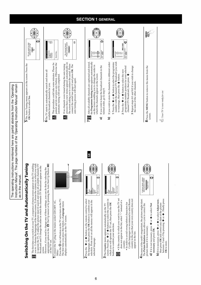
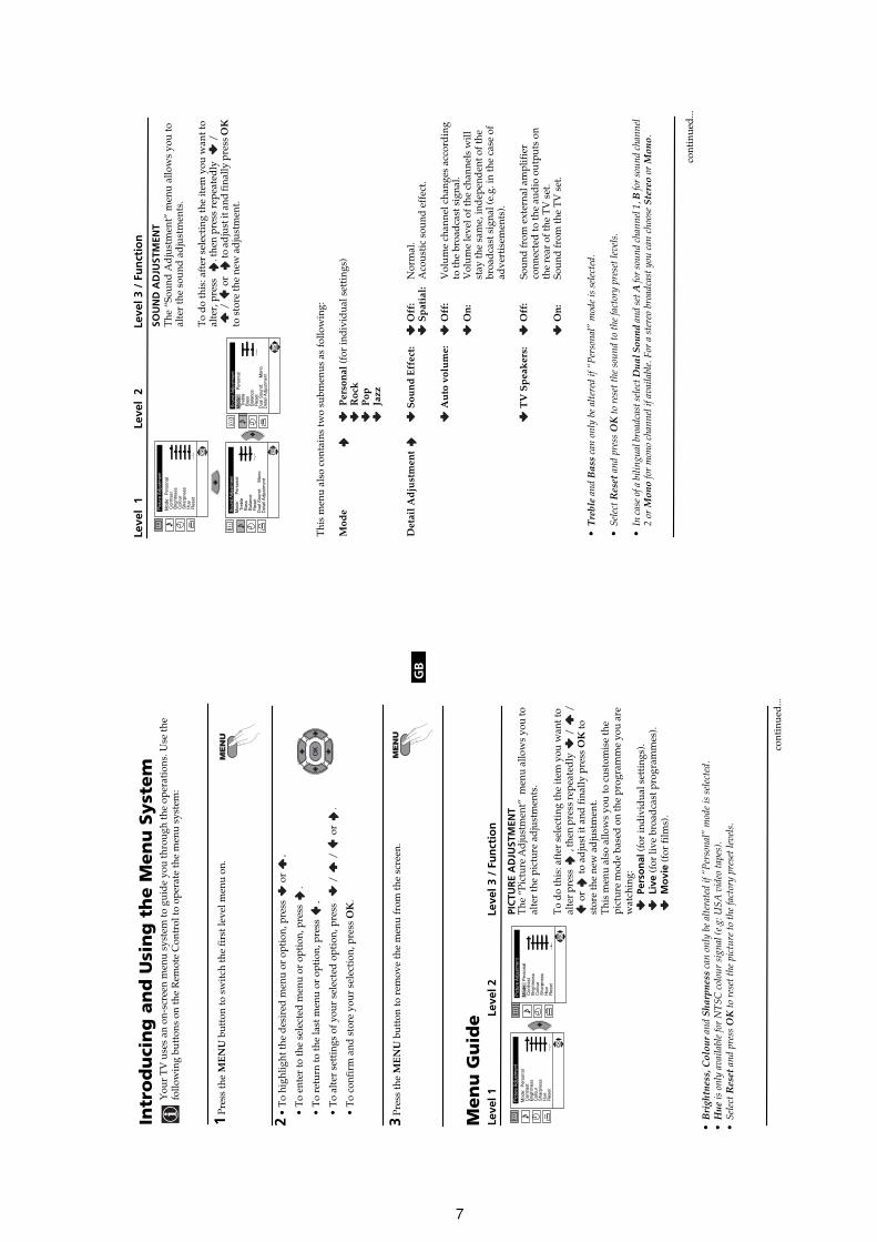
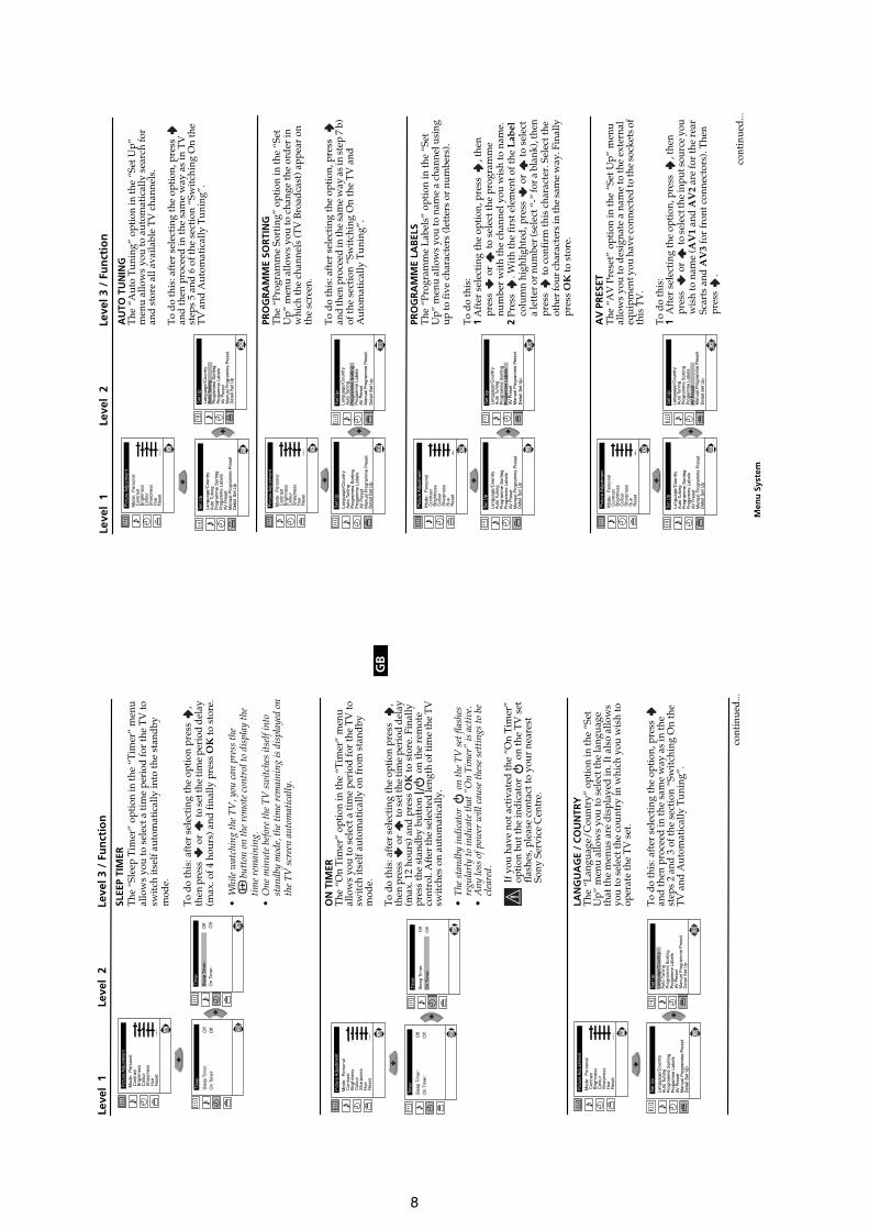


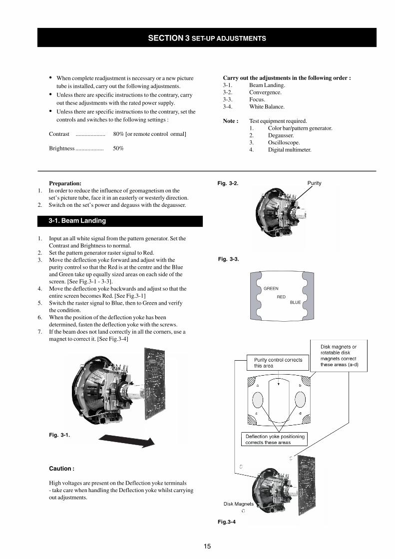


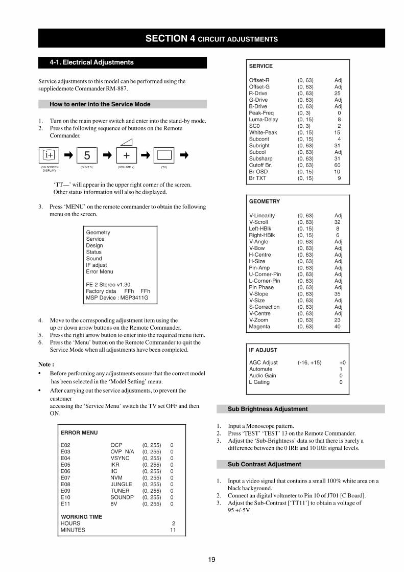
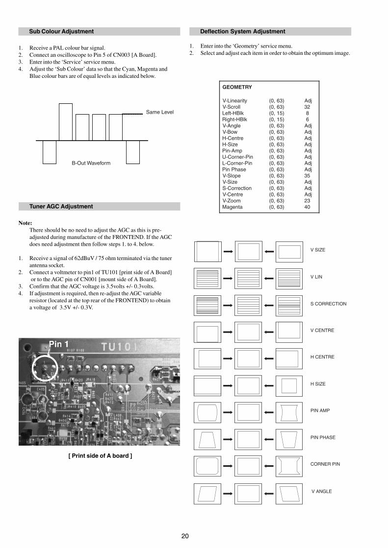


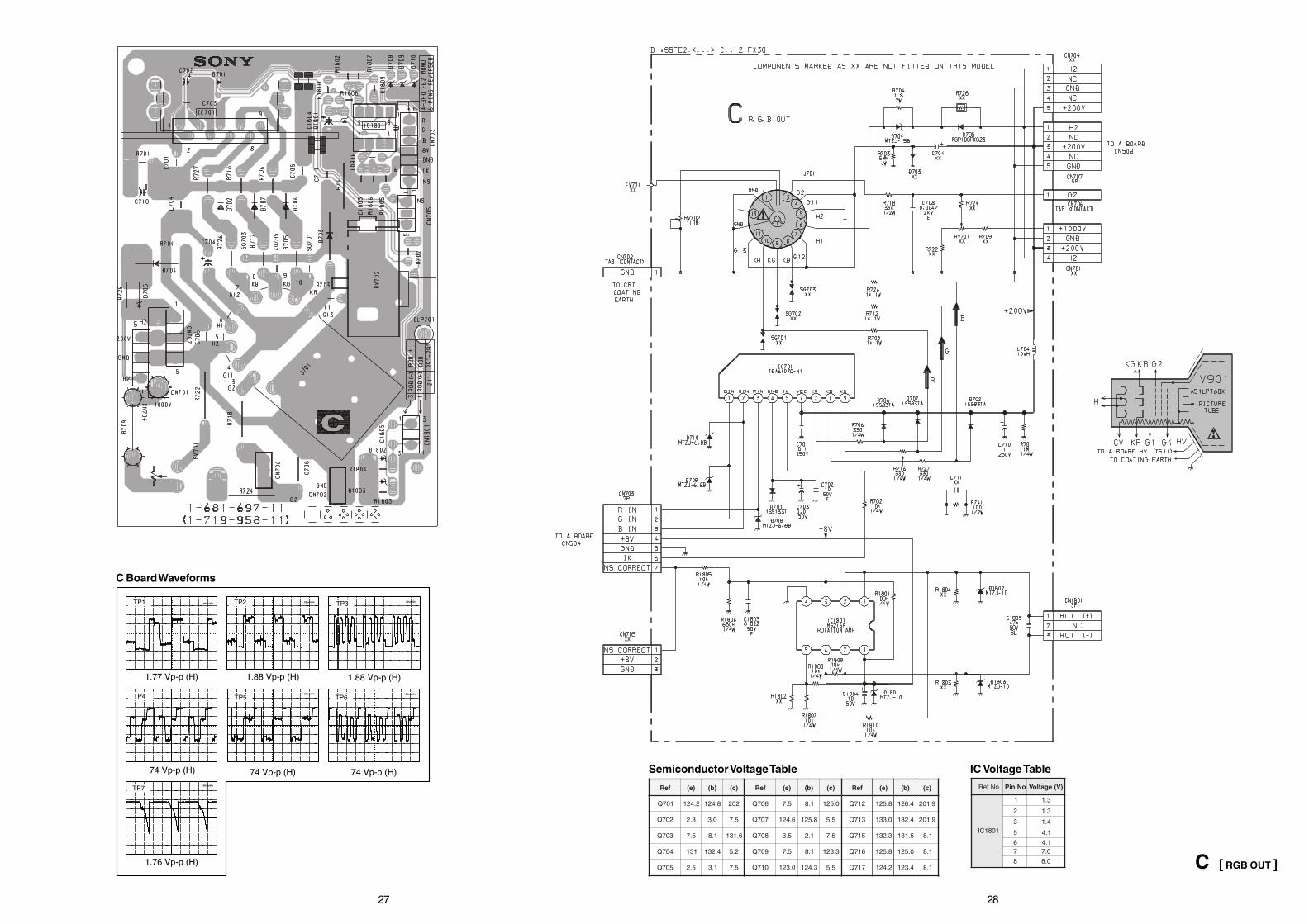
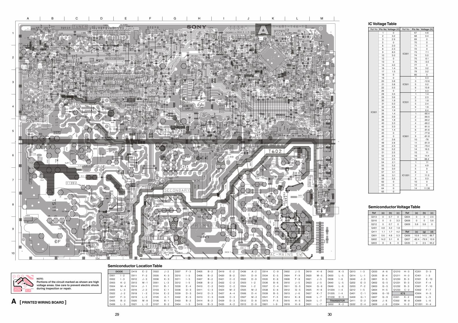


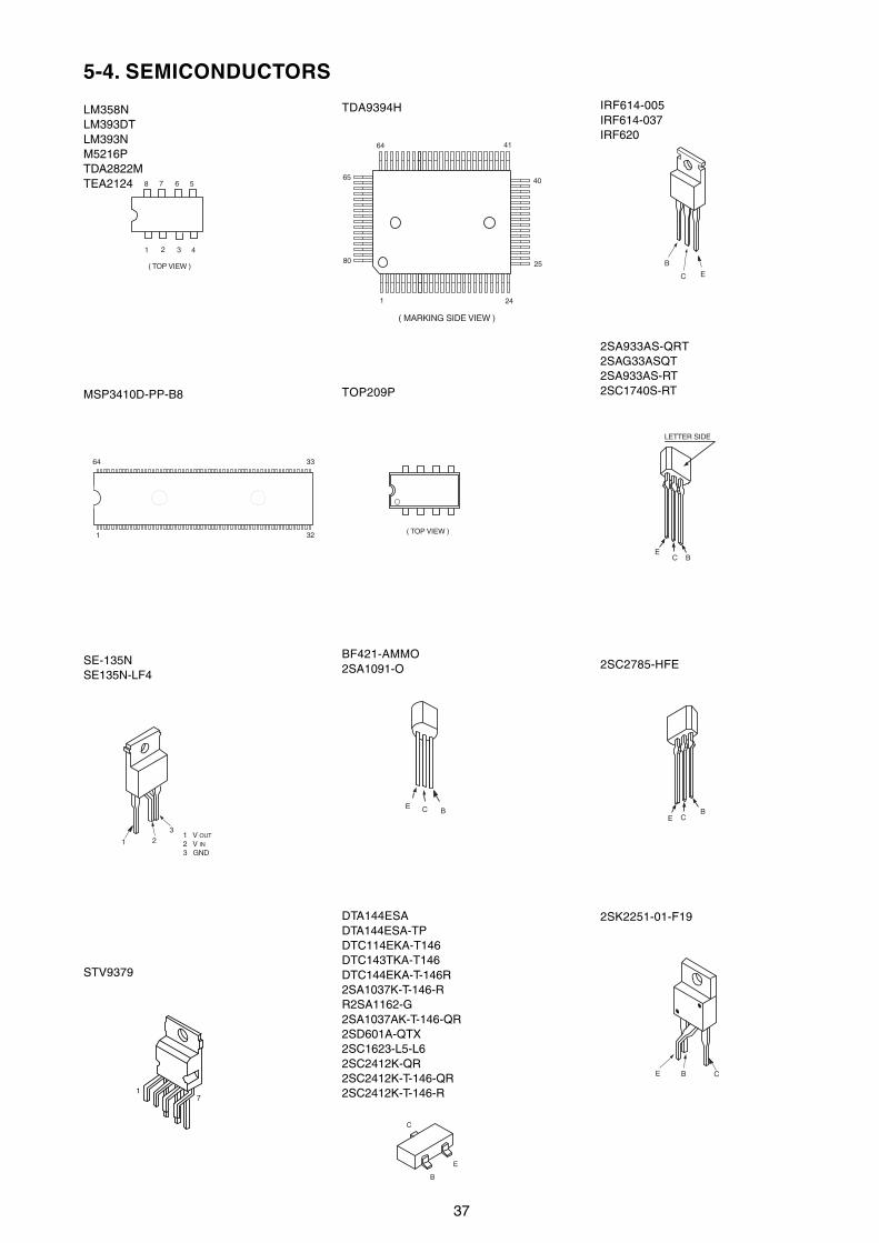


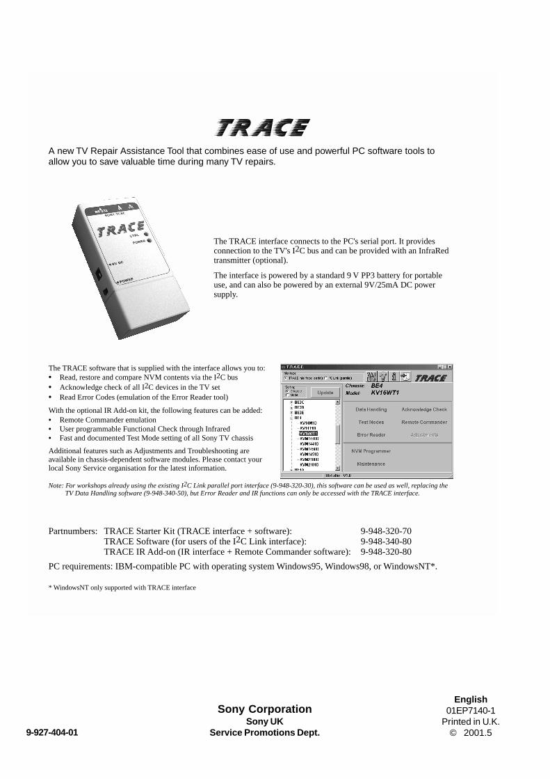


![Sony Kv-29se10b e k Bx-1l-Chassis [ET]](https://static.documents.pub/doc/80x56/55cf9926550346d0339be33d/sony-kv-29se10b-e-k-bx-1l-chassis-et.jpg)


