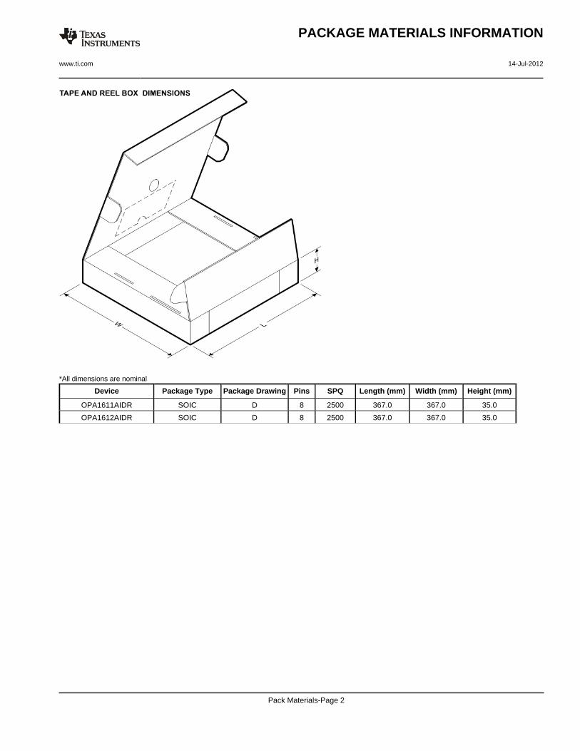
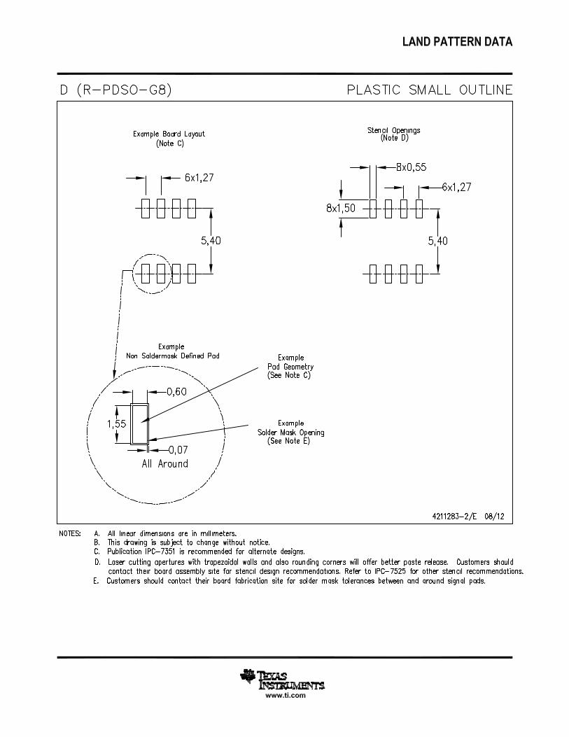
1FEATURES DESCRIPTIONThe OPA1611 (single) and OPA1612 (dual)
23• SUPERIOR SOUND QUALITYbipolar-input operational amplifiers achieve very low• ULTRALOW NOISE: 1.1nV/√Hz at 1kHz1.1nV/√Hz noise density with an ultralow distortion of• ULTRALOW DISTORTION: 0.000015% at 1kHz. The OPA1611 and OPA1612
0.000015% at 1kHz offer rail-to-rail output swing to within 600mV with a• HIGH SLEW RATE: 27V/μs 2kΩ load, which increases headroom and maximizes
dynamic range. These devices also have a high• WIDE BANDWIDTH: 40MHz (G = +1)output drive capability of ±30mA.• HIGH OPEN-LOOP GAIN: 130dB
• UNITY GAIN STABLE These devices operate over a very wide supply rangeof ±2.25V to ±18V, on only 3.6mA of supply current• LOW QUIESCENT CURRENT:per channel. The OPA1611 and OPA1612 op amps3.6mA PER CHANNELare unity-gain stable and provide excellent dynamic• RAIL-TO-RAIL OUTPUTbehavior over a wide range of load conditions.• WIDE SUPPLY RANGE: ±2.25V to ±18VThe dual version features completely independent• SINGLE AND DUAL VERSIONS AVAILABLEcircuitry for lowest crosstalk and freedom frominteractions between channels, even when overdrivenAPPLICATIONSor overloaded.
• PROFESSIONAL AUDIO EQUIPMENTBoth the OPA1611 and OPA1612 are available in• MICROPHONE PREAMPLIFIERS SO-8 packages and are specified from –40°C to
• ANALOG AND DIGITAL MIXING CONSOLES +85°C. SoundPlus™• BROADCAST STUDIO EQUIPMENT• AUDIO TEST AND MEASUREMENT• HIGH-END A/V RECEIVERS
1
Please be aware that an important notice concerning availability, standard warranty, and use in critical applications of TexasInstruments semiconductor products and disclaimers thereto appears at the end of this data sheet.
2SoundPlus is a trademark of Texas Instruments Incorporated.3All other trademarks are the property of their respective owners.
This integrated circuit can be damaged by ESD. Texas Instruments recommends that all integrated circuits be handled withappropriate precautions. Failure to observe proper handling and installation procedures can cause damage.
ESD damage can range from subtle performance degradation to complete device failure. Precision integrated circuits may be moresusceptible to damage because very small parametric changes could cause the device not to meet its published specifications.
ABSOLUTE MAXIMUM RATINGS (1)
Over operating free-air temperature range (unless otherwise noted).
VALUE UNIT
Supply Voltage VS = (V+) – (V–) 40 V
Input Voltage (V–) – 0.5 to (V+) + 0.5 V
Input Current (All pins except power-supply pins) ±10 mA
Output Short-Circuit (2) Continuous
Operating Temperature (TA) –55 to +125 °CStorage Temperature (TA) –65 to +150 °CJunction Temperature (TJ) 200 °C
Human Body Model (HBM) 3000 V
ESD Ratings Charged Device Model (CDM) 1000 V
Machine Model (MM) 200 V
(1) Stresses above these ratings may cause permanent damage. Exposure to absolute maximum conditions for extended periods maydegrade device reliability. These are stress ratings only, and functional operation of the device at these or any other conditions beyondthose specified is not supported.
(2) Short-circuit to VS/2 (ground in symmetrical dual supply setups), one amplifier per package.
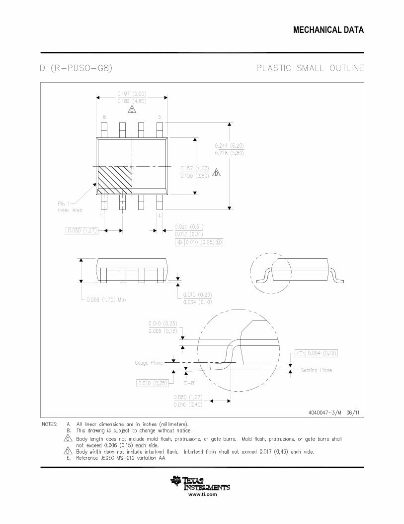
(1) For the most current package and ordering information see the Package Option Addendum at the end of this document, or see the TIweb site at www.ti.com.
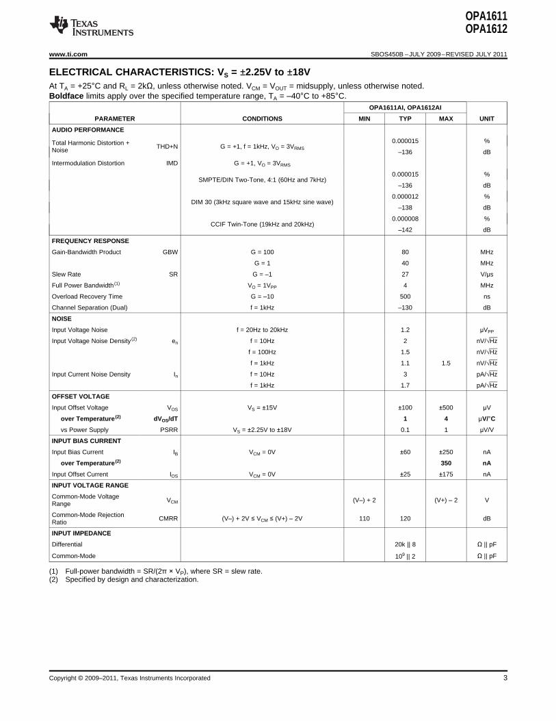
PIN CONFIGURATIONS
D PACKAGE D PACKAGEOPA1611, SO-8 OPA1612, SO-8
(TOP VIEW) (TOP VIEW)
(1) NC denotes no internal connection. Pin can be left floating or connected to any voltage between (V–) and (V+).
ELECTRICAL CHARACTERISTICS: VS = ±2.25V to ±18VAt TA = +25°C and RL = 2kΩ, unless otherwise noted. VCM = VOUT = midsupply, unless otherwise noted.Boldface limits apply over the specified temperature range, TA = –40°C to +85°C.
OPA1611AI, OPA1612AI
PARAMETER CONDITIONS MIN TYP MAX UNIT
AUDIO PERFORMANCE
0.000015 %Total Harmonic Distortion + THD+N G = +1, f = 1kHz, VO = 3VRMSNoise –136 dB
Intermodulation Distortion IMD G = +1, VO = 3VRMS
0.000015 %SMPTE/DIN Two-Tone, 4:1 (60Hz and 7kHz)
–136 dB
0.000012 %DIM 30 (3kHz square wave and 15kHz sine wave)
–138 dB
0.000008 %CCIF Twin-Tone (19kHz and 20kHz)
–142 dB
FREQUENCY RESPONSE
Gain-Bandwidth Product GBW G = 100 80 MHz
G = 1 40 MHz
Slew Rate SR G = –1 27 V/μs
Full Power Bandwidth (1) VO = 1VPP 4 MHz
Overload Recovery Time G = –10 500 ns
Channel Separation (Dual) f = 1kHz –130 dB
NOISE
Input Voltage Noise f = 20Hz to 20kHz 1.2 μVPP
Input Voltage Noise Density (2) en f = 10Hz 2 nV/√Hz
f = 100Hz 1.5 nV/√Hz
f = 1kHz 1.1 1.5 nV/√Hz
Input Current Noise Density In f = 10Hz 3 pA/√Hz
f = 1kHz 1.7 pA/√Hz
OFFSET VOLTAGE
Input Offset Voltage VOS VS = ±15V ±100 ±500 μV
over Temperature (2) dVOS/dT 1 4 μV/°C
vs Power Supply PSRR VS = ±2.25V to ±18V 0.1 1 μV/V
ELECTRICAL CHARACTERISTICS: VS = ±2.25V to ±18V (continued)At TA = +25°C and RL = 2kΩ, unless otherwise noted. VCM = VOUT = midsupply, unless otherwise noted.Boldface limits apply over the specified temperature range, TA = –40°C to +85°C.
OPA1611AI, OPA1612AI
PARAMETER CONDITIONS MIN TYP MAX UNIT
OPEN-LOOP GAIN
Open-Loop Voltage Gain AOL (V–) + 0.2V ≤ VO ≤ (V+) – 0.2V, RL = 10kΩ 114 130 dB
AOL (V–) + 0.6V ≤ VO ≤ (V+) – 0.6V, RL = 2kΩ 110 114 dB
OUTPUT
Voltage Output VOUT RL = 10kΩ, AOL ≥ 114dB (V–) + 0.2 (V+) – 0.2 V
RL = 2kΩ, AOL ≥ 110dB (V–) + 0.6 (V+) – 0.6 V
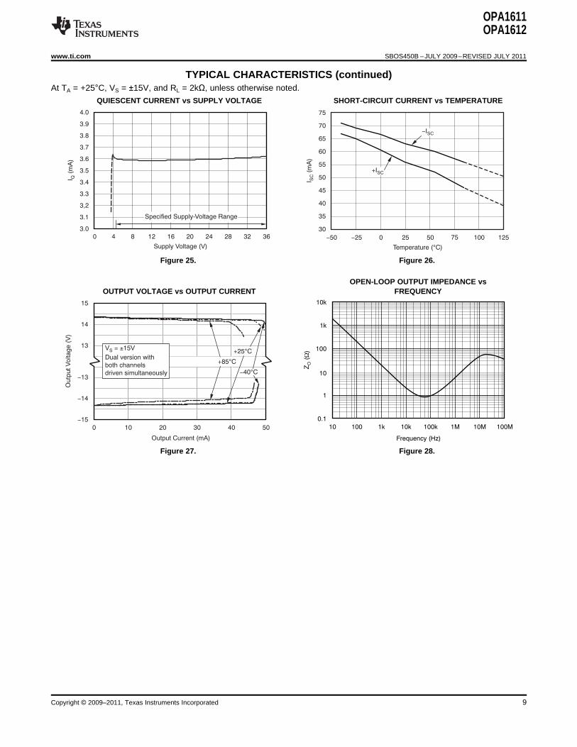
Output Current IOUT See Figure 27 mA
Open-Loop Output ZO See Figure 28 ΩImpedance
Short-Circuit Current ISC +55/–62 mA
Capacitive Load Drive CLOAD See Typical Characteristics pF
POWER SUPPLY
Specified Voltage VS ±2.25 ±18 V
Quiescent Current IQ IOUT = 0A 3.6 4.5 mA(per channel)
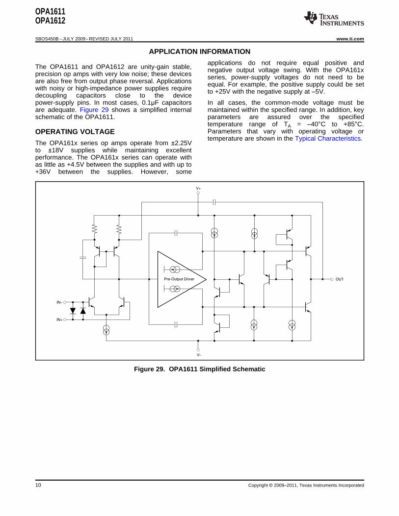
applications do not require equal positive andThe OPA1611 and OPA1612 are unity-gain stable, negative output voltage swing. With the OPA161xprecision op amps with very low noise; these devices series, power-supply voltages do not need to beare also free from output phase reversal. Applications equal. For example, the positive supply could be setwith noisy or high-impedance power supplies require to +25V with the negative supply at –5V.decoupling capacitors close to the devicepower-supply pins. In most cases, 0.1μF capacitors In all cases, the common-mode voltage must beare adequate. Figure 29 shows a simplified internal maintained within the specified range. In addition, keyschematic of the OPA1611. parameters are assured over the specified
temperature range of TA = –40°C to +85°C.Parameters that vary with operating voltage orOPERATING VOLTAGEtemperature are shown in the Typical Characteristics.
The OPA161x series op amps operate from ±2.25Vto ±18V supplies while maintaining excellentperformance. The OPA161x series can operate withas little as +4.5V between the supplies and with up to+36V between the supplies. However, some
INPUT PROTECTION current noise is negligible, and voltage noisegenerally dominates. The low voltage noise of the
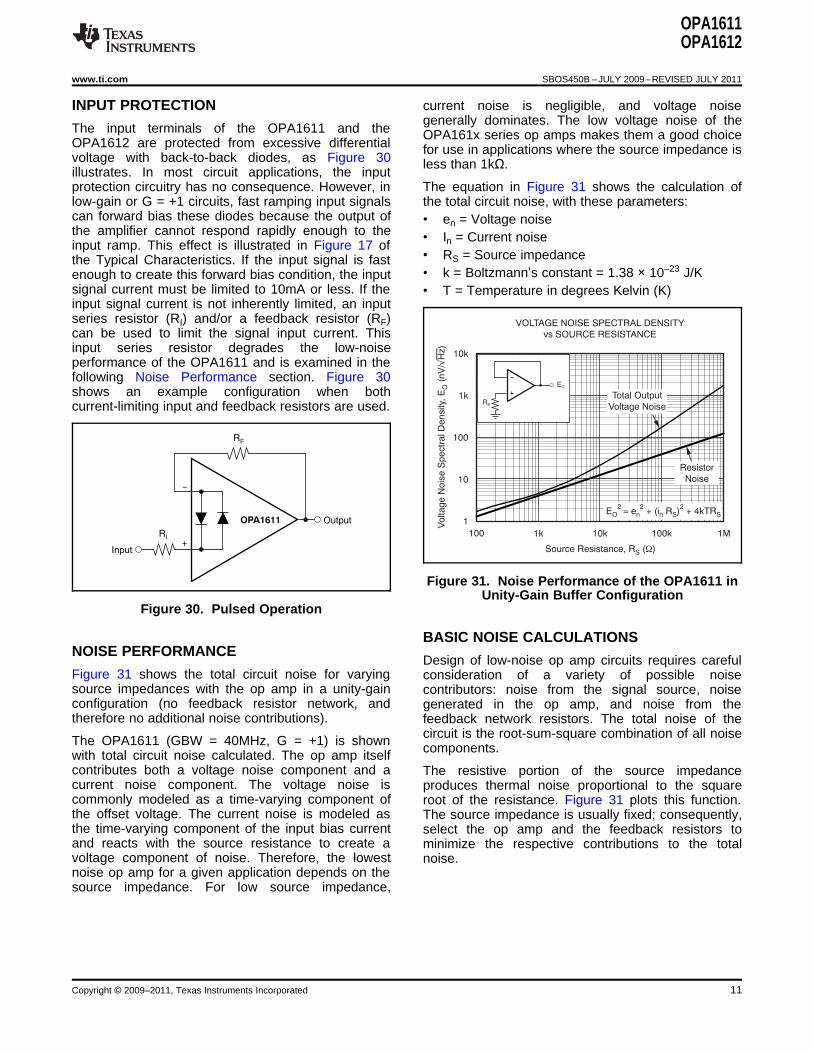
The input terminals of the OPA1611 and the OPA161x series op amps makes them a good choiceOPA1612 are protected from excessive differential for use in applications where the source impedance isvoltage with back-to-back diodes, as Figure 30 less than 1kΩ.illustrates. In most circuit applications, the inputprotection circuitry has no consequence. However, in The equation in Figure 31 shows the calculation oflow-gain or G = +1 circuits, fast ramping input signals the total circuit noise, with these parameters:can forward bias these diodes because the output of • en = Voltage noisethe amplifier cannot respond rapidly enough to the • In = Current noiseinput ramp. This effect is illustrated in Figure 17 of
• RS = Source impedancethe Typical Characteristics. If the input signal is fast• k = Boltzmann’s constant = 1.38 × 10⁻²³ J/Kenough to create this forward bias condition, the input
signal current must be limited to 10mA or less. If the • T = Temperature in degrees Kelvin (K)input signal current is not inherently limited, an inputseries resistor (RI) and/or a feedback resistor (RF)can be used to limit the signal input current. Thisinput series resistor degrades the low-noiseperformance of the OPA1611 and is examined in thefollowing Noise Performance section. Figure 30shows an example configuration when bothcurrent-limiting input and feedback resistors are used.
Figure 31. Noise Performance of the OPA1611 inUnity-Gain Buffer Configuration
Figure 30. Pulsed Operation
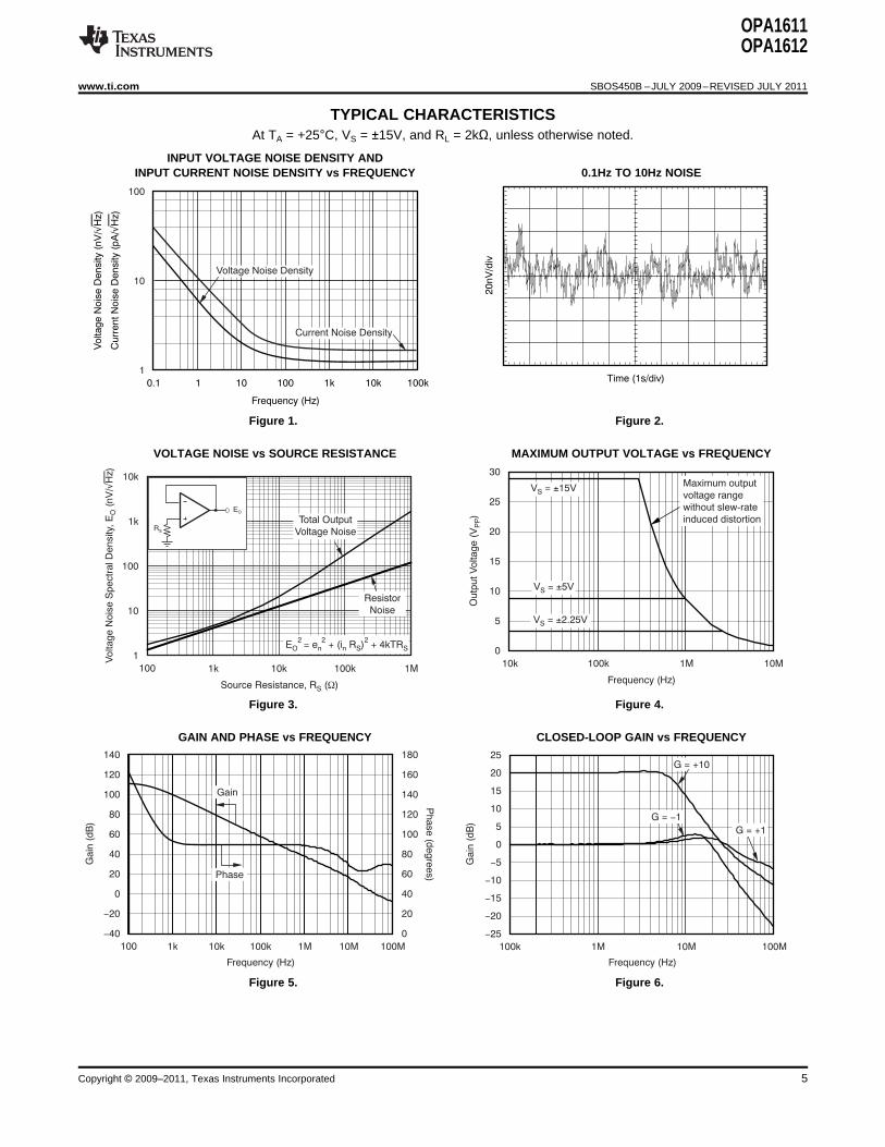
BASIC NOISE CALCULATIONSNOISE PERFORMANCE
Design of low-noise op amp circuits requires carefulFigure 31 shows the total circuit noise for varying consideration of a variety of possible noisesource impedances with the op amp in a unity-gain contributors: noise from the signal source, noiseconfiguration (no feedback resistor network, and generated in the op amp, and noise from thetherefore no additional noise contributions). feedback network resistors. The total noise of the
circuit is the root-sum-square combination of all noiseThe OPA1611 (GBW = 40MHz, G = +1) is shown components.with total circuit noise calculated. The op amp itselfcontributes both a voltage noise component and a The resistive portion of the source impedancecurrent noise component. The voltage noise is produces thermal noise proportional to the squarecommonly modeled as a time-varying component of root of the resistance. Figure 31 plots this function.the offset voltage. The current noise is modeled as The source impedance is usually fixed; consequently,the time-varying component of the input bias current select the op amp and the feedback resistors toand reacts with the source resistance to create a minimize the respective contributions to the totalvoltage component of noise. Therefore, the lowest noise.noise op amp for a given application depends on thesource impedance. For low source impedance,
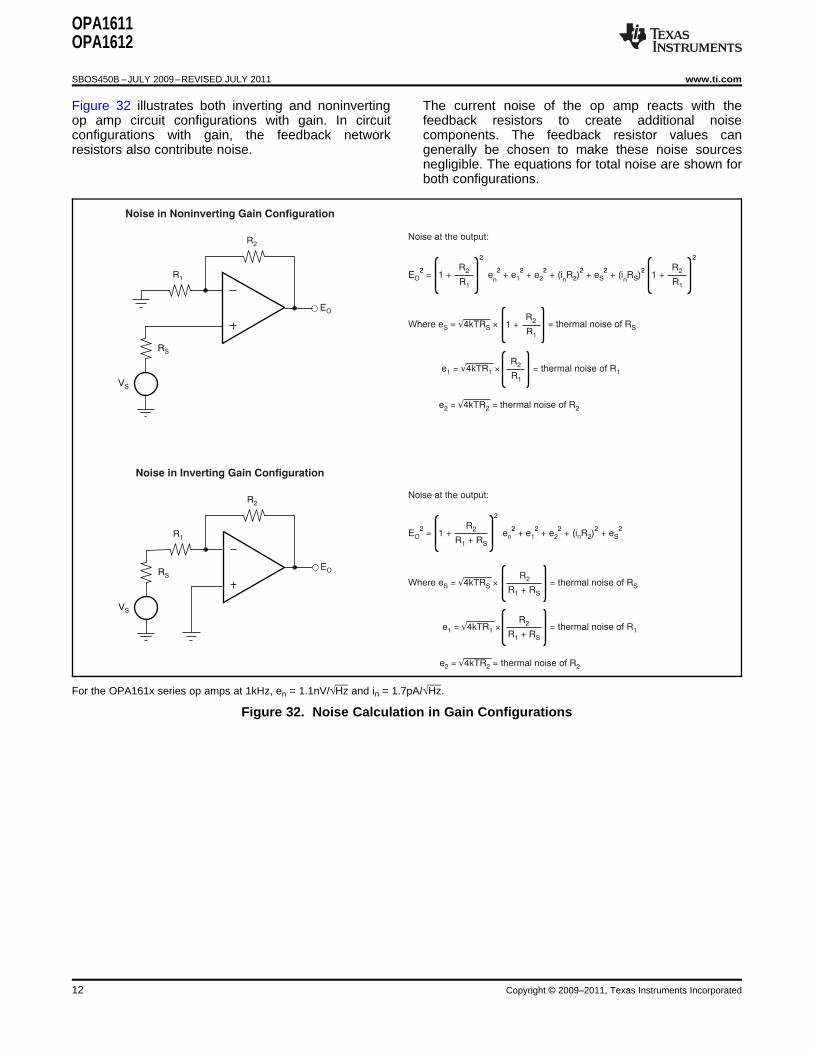
Figure 32 illustrates both inverting and noninverting The current noise of the op amp reacts with theop amp circuit configurations with gain. In circuit feedback resistors to create additional noiseconfigurations with gain, the feedback network components. The feedback resistor values canresistors also contribute noise. generally be chosen to make these noise sources
negligible. The equations for total noise are shown forboth configurations.
For the OPA161x series op amps at 1kHz, en = 1.1nV/√Hz and in = 1.7pA/√Hz.
Figure 32. Noise Calculation in Gain Configurations
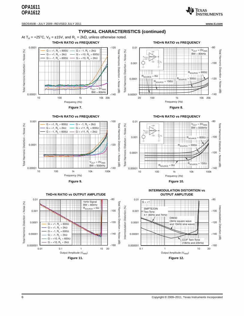
TOTAL HARMONIC DISTORTION Validity of this technique can be verified byMEASUREMENTS duplicating measurements at high gain and/or high
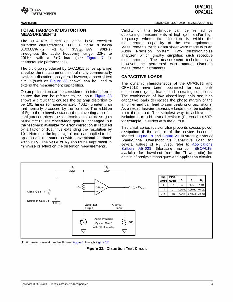
frequency where the distortion is within theThe OPA161x series op amps have excellent measurement capability of the test equipment.distortion characteristics. THD + Noise is below Measurements for this data sheet were made with an0.00008% (G = +1, VO = 3VRMS, BW = 80kHz) Audio Precision System Two distortion/noisethroughout the audio frequency range, 20Hz to analyzer, which greatly simplifies such repetitive20kHz, with a 2kΩ load (see Figure 7 for measurements. The measurement technique can,characteristic performance). however, be performed with manual distortion
measurement instruments.The distortion produced by OPA1611 series op ampsis below the measurement limit of many commerciallyavailable distortion analyzers. However, a special test CAPACITIVE LOADScircuit (such as Figure 33 shows) can be used to
The dynamic characteristics of the OPA1611 andextend the measurement capabilities.OPA1612 have been optimized for commonly
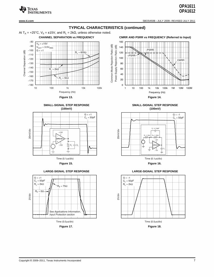
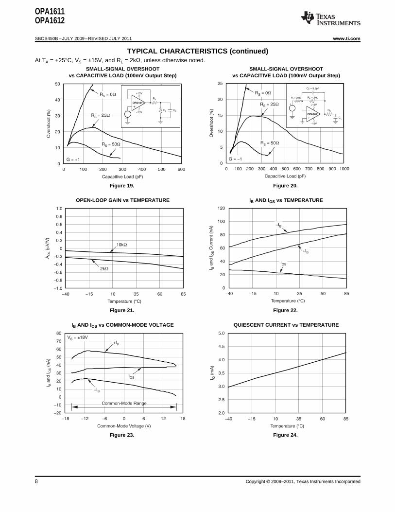
Op amp distortion can be considered an internal error encountered gains, loads, and operating conditions.source that can be referred to the input. Figure 33 The combination of low closed-loop gain and highshows a circuit that causes the op amp distortion to capacitive loads decreases the phase margin of thebe 101 times (or approximately 40dB) greater than amplifier and can lead to gain peaking or oscillations.that normally produced by the op amp. The addition As a result, heavier capacitive loads must be isolatedof R3 to the otherwise standard noninverting amplifier from the output. The simplest way to achieve thisconfiguration alters the feedback factor or noise gain isolation is to add a small resistor (RS equal to 50Ω,of the circuit. The closed-loop gain is unchanged, but for example) in series with the output.the feedback available for error correction is reduced
This small series resistor also prevents excess powerby a factor of 101, thus extending the resolution bydissipation if the output of the device becomes101. Note that the input signal and load applied to theshorted. Figure 19 and Figure 20 illustrate graphs ofop amp are the same as with conventional feedbackSmall-Signal Overshoot vs Capacitive Load forwithout R3. The value of R3 should be kept small toseveral values of RS. Also, refer to Applicationsminimize its effect on the distortion measurements.Bulletin AB-028 (literature number SBOA015,available for download from the TI web site) fordetails of analysis techniques and application circuits.
(1) For measurement bandwidth, see Figure 7 through Figure 12.
POWER DISSIPATION It is helpful to have a good understanding of thisbasic ESD circuitry and its relevance to an electrical
OPA1611 and OPA1612 series op amps are capable overstress event. Figure 34 illustrates the ESDof driving 2kΩ loads with a power-supply voltage up circuits contained in the OPA161x series (indicatedto ±18V. Internal power dissipation increases when by the dashed line area). The ESD protection circuitryoperating at high supply voltages. Copper leadframe involves several current-steering diodes connectedconstruction used in the OPA1611 and OPA1612 from the input and output pins and routed back to theseries op amps improves heat dissipation compared internal power-supply lines, where they meet at anto conventional materials. Circuit board layout can absorption device internal to the operational amplifier.also help minimize junction temperature rise. Wide This protection circuitry is intended to remain inactivecopper traces help dissipate the heat by acting as an during normal circuit operation.additional heat sink. Temperature rise can be furtherminimized by soldering the devices to the circuit An ESD event produces a short duration,board rather than using a socket. high-voltage pulse that is transformed into a short
duration, high-current pulse as it discharges througha semiconductor device. The ESD protection circuitsELECTRICAL OVERSTRESSare designed to provide a current path around the
Designers often ask questions about the capability of operational amplifier core to prevent it from beingan operational amplifier to withstand electrical damaged. The energy absorbed by the protectionoverstress. These questions tend to focus on the circuitry is then dissipated as heat.device inputs, but may involve the supply voltage pins
When an ESD voltage develops across two or moreor even the output pin. Each of these different pinof the amplifier device pins, current flows through onefunctions have electrical stress limits determined byor more of the steering diodes. Depending on thethe voltage breakdown characteristics of thepath that the current takes, the absorption deviceparticular semiconductor fabrication process andmay activate. The absorption device internal to thespecific circuits connected to the pin. Additionally,OPA1611 triggers when a fast ESD voltage pulse isinternal electrostatic discharge (ESD) protection isimpressed across the supply pins. Once triggered, itbuilt into these circuits to protect them fromquickly activates and clamps the ESD pulse to a safeaccidental ESD events both before and duringvoltage level.product assembly.
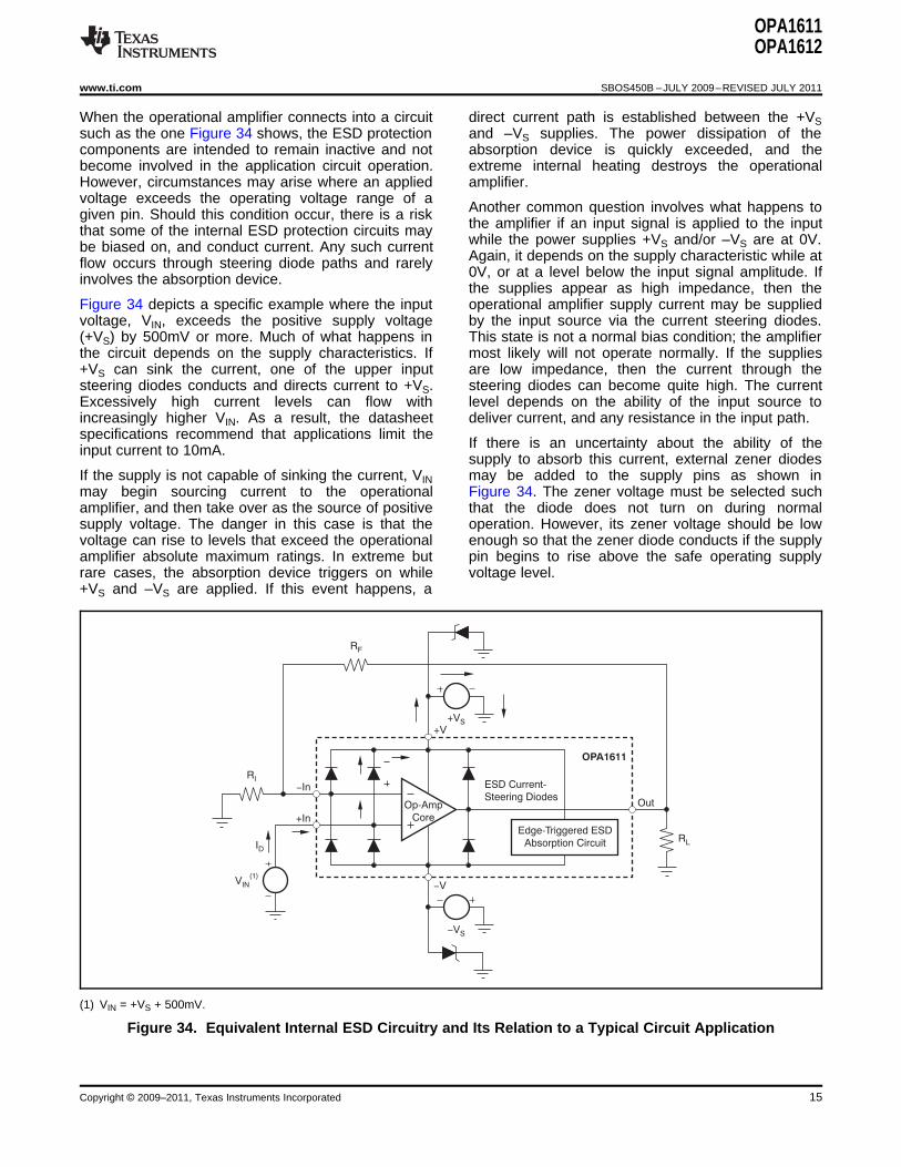
When the operational amplifier connects into a circuit direct current path is established between the +VSsuch as the one Figure 34 shows, the ESD protection and –VS supplies. The power dissipation of thecomponents are intended to remain inactive and not absorption device is quickly exceeded, and thebecome involved in the application circuit operation. extreme internal heating destroys the operationalHowever, circumstances may arise where an applied amplifier.voltage exceeds the operating voltage range of a
Another common question involves what happens togiven pin. Should this condition occur, there is a riskthe amplifier if an input signal is applied to the inputthat some of the internal ESD protection circuits maywhile the power supplies +VS and/or –VS are at 0V.be biased on, and conduct current. Any such currentAgain, it depends on the supply characteristic while atflow occurs through steering diode paths and rarely0V, or at a level below the input signal amplitude. Ifinvolves the absorption device.the supplies appear as high impedance, then the
Figure 34 depicts a specific example where the input operational amplifier supply current may be suppliedvoltage, VIN, exceeds the positive supply voltage by the input source via the current steering diodes.(+VS) by 500mV or more. Much of what happens in This state is not a normal bias condition; the amplifierthe circuit depends on the supply characteristics. If most likely will not operate normally. If the supplies+VS can sink the current, one of the upper input are low impedance, then the current through thesteering diodes conducts and directs current to +VS. steering diodes can become quite high. The currentExcessively high current levels can flow with level depends on the ability of the input source toincreasingly higher VIN. As a result, the datasheet deliver current, and any resistance in the input path.specifications recommend that applications limit the
If there is an uncertainty about the ability of theinput current to 10mA.supply to absorb this current, external zener diodes
If the supply is not capable of sinking the current, VIN may be added to the supply pins as shown inmay begin sourcing current to the operational Figure 34. The zener voltage must be selected suchamplifier, and then take over as the source of positive that the diode does not turn on during normalsupply voltage. The danger in this case is that the operation. However, its zener voltage should be lowvoltage can rise to levels that exceed the operational enough so that the zener diode conducts if the supplyamplifier absolute maximum ratings. In extreme but pin begins to rise above the safe operating supplyrare cases, the absorption device triggers on while voltage level.+VS and –VS are applied. If this event happens, a
(1) VIN = +VS + 500mV.
Figure 34. Equivalent Internal ESD Circuitry and Its Relation to a Typical Circuit Application
NOTE: Page numbers for previous revisions may differ from page numbers in the current version.
Changes from Revision A (August, 2009) to Revision B Page
• Revised Features list items ................................................................................................................................................... 1
• Added max specification for input voltage noise density at f = 1kHz ................................................................................... 3
• Corrected typo in footnote 1 for Electrical Characteristics .................................................................................................... 3
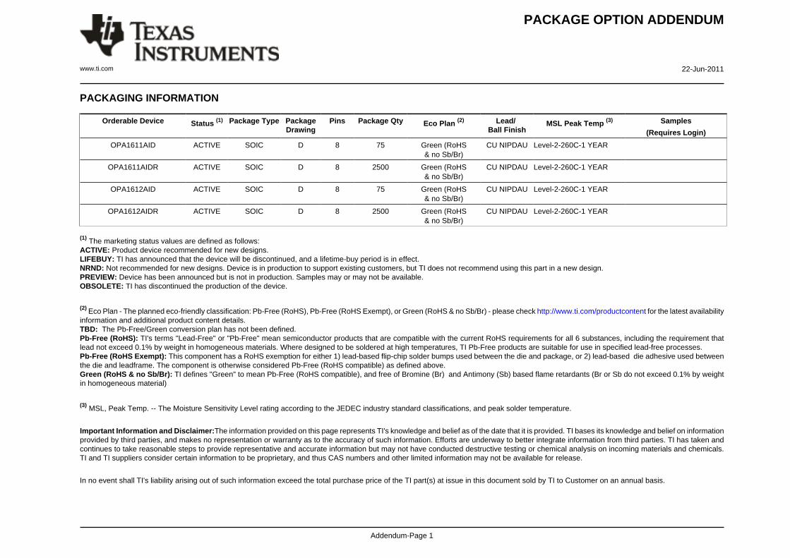
Orderable Device Status (1) Package Type PackageDrawing
Pins Package Qty Eco Plan (2) Lead/Ball Finish
MSL Peak Temp (3) Samples
(Requires Login)
OPA1611AID ACTIVE SOIC D 8 75 Green (RoHS& no Sb/Br)
CU NIPDAU Level-2-260C-1 YEAR
OPA1611AIDR ACTIVE SOIC D 8 2500 Green (RoHS& no Sb/Br)
CU NIPDAU Level-2-260C-1 YEAR
OPA1612AID ACTIVE SOIC D 8 75 Green (RoHS& no Sb/Br)
CU NIPDAU Level-2-260C-1 YEAR
OPA1612AIDR ACTIVE SOIC D 8 2500 Green (RoHS& no Sb/Br)
CU NIPDAU Level-2-260C-1 YEAR
(1) The marketing status values are defined as follows:ACTIVE: Product device recommended for new designs.LIFEBUY: TI has announced that the device will be discontinued, and a lifetime-buy period is in effect.NRND: Not recommended for new designs. Device is in production to support existing customers, but TI does not recommend using this part in a new design.PREVIEW: Device has been announced but is not in production. Samples may or may not be available.OBSOLETE: TI has discontinued the production of the device.
(2) Eco Plan - The planned eco-friendly classification: Pb-Free (RoHS), Pb-Free (RoHS Exempt), or Green (RoHS & no Sb/Br) - please check http://www.ti.com/productcontent for the latest availabilityinformation and additional product content details.TBD: The Pb-Free/Green conversion plan has not been defined.Pb-Free (RoHS): TI's terms "Lead-Free" or "Pb-Free" mean semiconductor products that are compatible with the current RoHS requirements for all 6 substances, including the requirement thatlead not exceed 0.1% by weight in homogeneous materials. Where designed to be soldered at high temperatures, TI Pb-Free products are suitable for use in specified lead-free processes.Pb-Free (RoHS Exempt): This component has a RoHS exemption for either 1) lead-based flip-chip solder bumps used between the die and package, or 2) lead-based die adhesive used betweenthe die and leadframe. The component is otherwise considered Pb-Free (RoHS compatible) as defined above.Green (RoHS & no Sb/Br): TI defines "Green" to mean Pb-Free (RoHS compatible), and free of Bromine (Br) and Antimony (Sb) based flame retardants (Br or Sb do not exceed 0.1% by weightin homogeneous material)
(3) MSL, Peak Temp. -- The Moisture Sensitivity Level rating according to the JEDEC industry standard classifications, and peak solder temperature.
Important Information and Disclaimer:The information provided on this page represents TI's knowledge and belief as of the date that it is provided. TI bases its knowledge and belief on informationprovided by third parties, and makes no representation or warranty as to the accuracy of such information. Efforts are underway to better integrate information from third parties. TI has taken andcontinues to take reasonable steps to provide representative and accurate information but may not have conducted destructive testing or chemical analysis on incoming materials and chemicals.TI and TI suppliers consider certain information to be proprietary, and thus CAS numbers and other limited information may not be available for release.
In no event shall TI's liability arising out of such information exceed the total purchase price of the TI part(s) at issue in this document sold by TI to Customer on an annual basis.
Texas Instruments Incorporated and its subsidiaries (TI) reserve the right to make corrections, enhancements, improvements and otherchanges to its semiconductor products and services per JESD46, latest issue, and to discontinue any product or service per JESD48, latestissue. Buyers should obtain the latest relevant information before placing orders and should verify that such information is current andcomplete. All semiconductor products (also referred to herein as “components”) are sold subject to TI’s terms and conditions of salesupplied at the time of order acknowledgment.
TI warrants performance of its components to the specifications applicable at the time of sale, in accordance with the warranty in TI’s termsand conditions of sale of semiconductor products. Testing and other quality control techniques are used to the extent TI deems necessaryto support this warranty. Except where mandated by applicable law, testing of all parameters of each component is not necessarilyperformed.
TI assumes no liability for applications assistance or the design of Buyers’ products. Buyers are responsible for their products andapplications using TI components. To minimize the risks associated with Buyers’ products and applications, Buyers should provideadequate design and operating safeguards.
TI does not warrant or represent that any license, either express or implied, is granted under any patent right, copyright, mask work right, orother intellectual property right relating to any combination, machine, or process in which TI components or services are used. Informationpublished by TI regarding third-party products or services does not constitute a license to use such products or services or a warranty orendorsement thereof. Use of such information may require a license from a third party under the patents or other intellectual property of thethird party, or a license from TI under the patents or other intellectual property of TI.
Reproduction of significant portions of TI information in TI data books or data sheets is permissible only if reproduction is without alterationand is accompanied by all associated warranties, conditions, limitations, and notices. TI is not responsible or liable for such altereddocumentation. Information of third parties may be subject to additional restrictions.
Resale of TI components or services with statements different from or beyond the parameters stated by TI for that component or servicevoids all express and any implied warranties for the associated TI component or service and is an unfair and deceptive business practice.TI is not responsible or liable for any such statements.
Buyer acknowledges and agrees that it is solely responsible for compliance with all legal, regulatory and safety-related requirementsconcerning its products, and any use of TI components in its applications, notwithstanding any applications-related information or supportthat may be provided by TI. Buyer represents and agrees that it has all the necessary expertise to create and implement safeguards whichanticipate dangerous consequences of failures, monitor failures and their consequences, lessen the likelihood of failures that might causeharm and take appropriate remedial actions. Buyer will fully indemnify TI and its representatives against any damages arising out of the useof any TI components in safety-critical applications.
In some cases, TI components may be promoted specifically to facilitate safety-related applications. With such components, TI’s goal is tohelp enable customers to design and create their own end-product solutions that meet applicable functional safety standards andrequirements. Nonetheless, such components are subject to these terms.
No TI components are authorized for use in FDA Class III (or similar life-critical medical equipment) unless authorized officers of the partieshave executed a special agreement specifically governing such use.
Only those TI components which TI has specifically designated as military grade or “enhanced plastic” are designed and intended for use inmilitary/aerospace applications or environments. Buyer acknowledges and agrees that any military or aerospace use of TI componentswhich have not been so designated is solely at the Buyer's risk, and that Buyer is solely responsible for compliance with all legal andregulatory requirements in connection with such use.
TI has specifically designated certain components which meet ISO/TS16949 requirements, mainly for automotive use. Components whichhave not been so designated are neither designed nor intended for automotive use; and TI will not be responsible for any failure of suchcomponents to meet such requirements.
Products Applications
Audio www.ti.com/audio Automotive and Transportation www.ti.com/automotive
Amplifiers amplifier.ti.com Communications and Telecom www.ti.com/communications
Data Converters dataconverter.ti.com Computers and Peripherals www.ti.com/computers