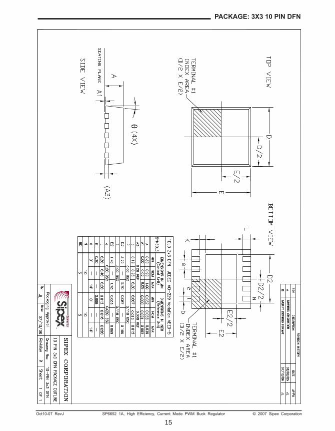
Features1A Output Current1.4MHz Constant Frequency Operation97% Efficiency Possible 0.5µA (Max.) Shutdown Current Adjustable Output Voltage No External FETs or Schottky Diode Required Uses Small Value Inductors and Ceramic Output Capacitors Low Dropout Operation: 100% Duty Cycle Soft Start and Thermal Shutdown Protection Easy Frequency Synchonization Lead Free, RoHS Compliant package: l Small (3mm X 3mm) 10 Pin DFN or MSOP
applications Mobile Phones PDAs DSCs MP3 Players USB Devices Point of Use Power
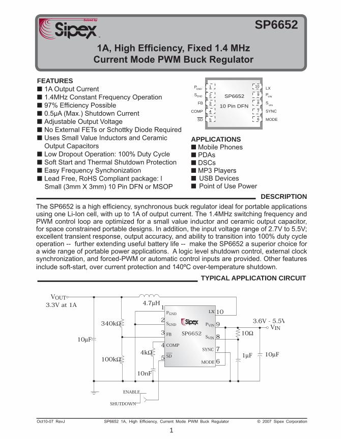
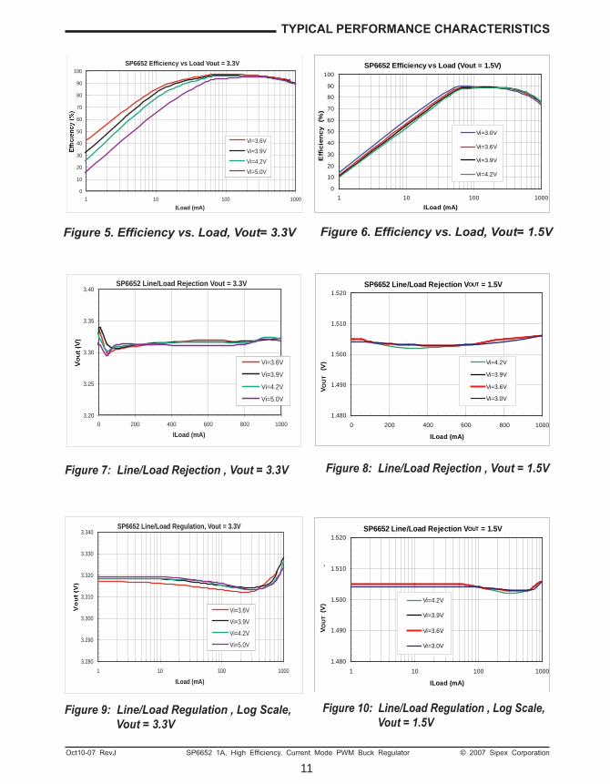
The SP6652 is a high efficiency, synchronous buck regulator ideal for portable applications using one Li-Ion cell, with up to 1A of output current. The 1.4MHz switching frequency and PWM control loop are optimized for a small value inductor and ceramic output capacitor, for space constrained portable designs. In addition, the input voltage range of 2.7V to 5.5V; excellent transient response, output accuracy, and ability to transition into 100% duty cycle operation -- further extending useful battery life -- make the SP6652 a superior choice for a wide range of portable power applications. A logic level shutdown control, external clock synchronization, and forced-PWM or automatic control inputs are provided. Other features include soft-start, over current protection and 140ºC over-temperature shutdown.
typical application circuit
Description
1A, High Efficiency, Fixed 1.4 MHz Current Mode PWM Buck Regulator
PVIN,SVIN ...........................................................................-0.3V to 6.0VPGND to SGND .....................................................................-0.3V to 0.3VLX to PGND .............................................................. - 0.3V to PVIN+0.3VStorage Temperature ....................................................-65 °C to 150 °COperating Temperature .................................................. -40°C to +85°C
ABSOLUTE MAXIMUM RATINGSThese are stress ratings only and functional operation of the device atthese ratings or any other above those indicated in the operation sec-tions of the specifications below is not implied. Exposure to absolute maximum rating conditions for extended periods of time may affect reliability.
electrical cHaracteristicsVIN = UVIN = VSDN = 3.6V, IO = 0mA, TAMB = -40°C to +85°C, typical values at 27°C unless otherwise noted. The ♦ denotes the specifications which apply over the full temperature range, unless otherwise specified.
PARAMETER MIN typ MAX units conDitions
Input Operating Voltage 2.85 5.5 V ♦ Result of IQ measurement at VIN = PVIN = 5.5V
FB Set Voltage 0.784 0.8 0.816 V ♦FB Set Current - 0.0 µA ♦ VFB = 0.8V
PGNDPower Ground Pin. Synchronous rectifier current returns through this pin.
SGND Internal Ground Pin. Control circuitry returns current to this pin.
3 FBExternal feedback network input connection. Connect a resistor from FB to ground and from FB to VOUT to control the output voltage. Regulation point at FB = 0.8V Typical.
4 COMP Compensation pin for error loop. Connect an R and C in series to ground to control open loop pole and zero.
5 SD Shutdown control input. Tie pin to VIN for normal operation, tie to ground for shutdown. TTL input threshold.
6 MODE Connect this pin to VIN.
7 SYNC An external clock signal can be connected to this pin to synchronize the switching frequency.
8 SVINInternal supply voltage. Control circuitry is powered from from this pin. Use an RC filter close to the pin to cut down supply noise.
9 PVINSupply voltage for the output driver stage. Inductor charging current passes through this pin.
0 LX Inductor switching node. Inductor tied between this pin and the output capacitor to create regulated output voltage.
Current Mode Control and Slope CompensationThe SP6652 is designed to use low value ceramic capacitors and low value inductors to reduce the converter’s volume and cost in portable devices. Current mode PWM control was, therefore, chosen for the ease of compensation when using ceramic output capacitors and better transient line rejec-tion, which is important in battery powered applications. Current mode control spreads the two poles of the output power train filter far apart so that the modulator gain crosses over at -20dB/decade instead of the usual -40dB/decade. The external compensation network is, simply, a series RC circuit con-nected between ground and the output of the internal transconductance error amplifier.
It is well known that an unconditional insta-bility exists for any fixed frequency current-mode converter operating above 50% duty cycle. A simple, constant-slope compensa-tion is chosen to achieve stability under these conditions. The most common high duty cycle application is a Li-Ion battery powered regulator with a 3.3V output (D ≥ 90%). Since the current loop is critically damped when the compensation slope (denoted MCV) equals the negative discharge slope (denoted M2V), the amount of slope compensation chosen is, therefore:
The inductor current is sensed as a voltage across the PMOS charging switch and the NMOS synchronous rectifier (see BLOCK DIAGRAM). During inductor current charge, V(PVIN)-V(LX) represents the charging cur-
rent ramp times the resistance of the PMOS charging switch. To keep the effective current slope compensation constant (remembering current is being compensated, not voltage) the voltage slope must be proportional to RPMOS. To account for this, the slope com-pensation voltage is internally generated with a bias current that is also proportional to RPMOS.
Over Current ProtectionIn steady state closed loop operation the voltage at the COMP pin controls the duty cycle. Due to the current mode control and the slope compensation, this voltage will be:
V(COMP)•ILPK•RPMOS + MCV•TON + VBE(Q1)
The COMP node will be clamped when its voltage tries to exceed V(BLIM) + VBE(Q1). The VBE(Q1) term is cancelled by VBE(Q2) at the output of the translator. The correct value of clamp voltage is, therefore:
V(BLIM) = IL(MAX)• RPMOS + MCV •TON
The IL(MAX) term is generated with a bias current that is proportional to RPMOS, to keep the value of current limit approximately constant over process and temperature variations, while the MCV •TON is generated by a peak-holding circuit that senses the amplitude of the slope compensation ramp at the end of TON.
There is minimum on-time (TON) generated even if the COMP node is at zeroV, since the peak current comparator is reset at the end of a charge cycle and is held low during a blanking time after the start of the next charge cycle. This is necessary to swamp the transients in the inductor current ramp around switching times. The minimum TON (100ns, nominally) is not sufficient for the COMP node to keep control of the current
when the output voltage is low. The inductor current tends to rise until the energy loss from the discharge resistances are equal to the energy gained during the charge phase. For this reason, the clock frequency is cut in half when the feedback pin is below 0.3V, ef-fectively reducing the minimum duty cycle in half. Above V(FB) = 0.3V the clock frequency is normal (see Typical Operating Character-istics: Inductor Current vs. VOUT)
Voltage Loop and Compensation in PWM ModeThe voltage loop section of the circuit con-sists of the error amplifier and the translator circuits (see functional diagram). The input of the voltage loop is the 0.8V reference volt-age minus the divided down output voltage at the feedback pin. The output of the error amplifier is translated from a ground referred signal (the COMP node) to a power input voltage referred signal. The output of the voltage loop is fed to the positive terminal of the Current Loop comparator, and repre-sents the peak inductor current necessary to close the loop.
The total power supply loop is compensated with a series RC network connected from the COMP pin to ground. Compensation is simple due to current-mode control. The modulator has two dominant poles: one at a low frequency, and one above the crossover frequency of the loop, as seen in the graph below, Linearized Modulator Frequency Response vs. Inductor Value.
The low frequency pole for L1= 5µH is 4kHz, the second pole is 500kHz, and the gain-bandwidth is 20kHz. The total loop crossover frequency is chosen to be 200kHz, which is 1/6th of the clock frequency. This sets the second modulator pole at 2.5 times the crossover frequency. Therefore the gain of the error amplifier can be 200kHz/20kHz = 10 at the first modulator pole of 4kHz. The error amp transconductance is 1mA/V, so this sets the RZ resistor value in the com-pensation network at 10/1mA/V = 10kΩ. The zero frequency is placed at the first pole to provide at total system response of -20dB/decade (the zero from the error amp cancels the first modulator pole, leaving the
1 pole rolloff from the error amp pole). The compensation capacitor becomes:
Cc = =
(2π•Rz•pole1) (6.28•10kΩ•4kHz) = 4nF
Soft StartSoft-start is accomplished by disconnect-ing the error amp and inserting a constant 2μA current to charge the compensation capacitor. When power is first applied and the reference establishes, the clamp circuit at the COMP node sets its voltage at one VBE, which is the bottom of the inductor current range. The soft-start current continues to charge up the COMP node, slowly raising the inductor cur-rent level. The inductor current will increase at approximately:
For typical circuit values of CC=6.8nF and RZ=8kΩ, the soft start period is TBD ms.
The inductor current will eventually rise above the required load current and the out-put voltage will charge up. During soft-start the error amp is disconnected and acts as a comparator. When V(FB) rises above the reference, the error amp switches to logic high and ends soft-start, at which point the error amp output is connected to the capaci-tated COMP node.
DetaileD Description
The switching frequency will be reduced to half the normal frequency as long as V(FB) is below 0.3V, as previously discussed in the Over Current Protection section.
100% Duty Cycle in Dropout To extend the battery life in portable applica-tions, the PWM control logic is set up such that if the output SR latch has not been reset by the Current Loop comparator at the end of a clock cycle, the charge signal continues to stay high into the beginning of the next cycle. This will happen naturally when the converter starts to go into dropout. The slope compensation ramp is reset every cycle.
External Clock Synchronization
The SP6652 has an internal 1.4MHz clock that can be defeated by connecting an ex-ternal clock pulse on the SYNC. The capture range for clock synchronization is 1.0 to 2.0MHz. When a clock pulse is present on the SYNC pin, the internal oscillator bias current is scaled back, handing control of the clock pulses to the faster external clock. The pulse width of the clock is approximately 50 ns, whether internally generated or ex-ternally applied.
Thermal Shutdown
The internal die temperature is monitored by a comparator that issues a “TOO HOT” sig-nal when the junction temperature reaches 140˚C, nominally. This signal that inhibits all internal circuits until the temperature has decreased to approximately 135˚C, at which point a normal soft start sequence is initiated.
The SP6652 PWM buck regulator circuit requires 3 capacitors: 10µF for the PVIN input, 1µF input bypass for the SVIN and 10µF for the output are typically recommended. For the input capacitor, a value even larger than 10µF will help reduce input voltage ripple for applications sensitive to ripple on the battery voltage. See the Typical Per-formance Characteristics section for wave-forms on input and output ripple with 10µF capacitors. All the capacitors should be surface mount ceramic for low lead induc-tance necessary at the 1.4MHz switching frequency of the SP6652 and to obtain low ESR. This also helps improve bypassing on the input pin and ripple on the output. Ceramic capacitors with X5R or X7R tem-perature grade are recommended for most applications. A selection of recommended capacitors is included in Table 1. The 1µF SVIN input capacitor should have a series resistor of about 10Ω value connected from the input to the SVIN pin to form an RC low pass filter to remove high frequency spikes present on the input switching pin
COMPONENT SELECTIONPVIN. This will keep the SP6652 internal reference and other sensitive circuits noise free and ensure better output regulation. The GND returns for the PVIN capacitor and the output capacitor should be connected directly to the PGND pin, which should con-nect to the thermal pad ground located un-der the SP6652. The GND return for the 1µF SVIN capacitor should be connected to the SGND pin, which should be connected separately to the PGND pin to avoid adding PGND noise to the SP6652 SGND pin. See the Typical SP6652 Circuit Layout for de-tails on the recommended layout.
Output Voltage SelectionTo set the output voltage for the SP6652, a pair of resistors, RF and RI are used as a voltage divider between the output voltage at the output capacitor and the FB pin and GND, as shown in the typical application cir-cuit. The recommended value for the RI re-sistor is 100KΩ to 200KΩ to keep the quies-cent current low, but not have the impedance too high at the FB pin for good regulation.
The range of typical inductor values and sizes are shown here in Table 2.
The output voltage can be set using the formula:VOUT = VFB*( + RF/RI)
Where VFB = 0.8V typically, and for no-load Ton is kept within 200nsec Minimum: Ton(min) = VOUT/(VIN *Freq).
Compensation Component Selection
For simplicity in compensation with ce-ramic output capacitors, the SP6652 uses current mode PWM control, so all that is needed for stability is a series RZ and CC at the COMP pin to compensate the error amplifier. To see the actual SP6652 re-sponse with frequency, in figure 3 we have taken a bode plot of gain and frequency re-sponse of the SP6652 circuit with 3.3Vout. Looking first at the SP6652 Modulator Gain at low frequency you see a constant gain of about 26dB and the first pole or -3dB point at about 4 kHz, where the slope of the gain curve becomes about -20dB/de-cade. At high frequency on the SP6652 Modulator Gain curve one can see the modulator curve slope increase down-
ward for a high frequency pole at about 150KHz, which is widely separated in frequency from the low frequency 4kHz pole, so that the SP6652 can be compen-sated by a zero at the low frequency pole where the gain slope is only -20dB/decade. The gain for the error amplifier is the cross-
Figure 3. SP6652 Gain and Frequency Response 3.3V output voltage
Manufacturers/ Website Part Number Capacitance/ Voltage
over frequency fzero = 80kHz (from the Bode plot) divided by the loop gain band-width, given as 20kHz, which is used in the following equation:
Error Amp Gain = fzero / (loop gain bandwidth) = 80kHz / 20kHz = 4
The error amp transconductance is about 1mS, so this sets the RZ resistor to be:
Rz = 4/1mS = 4KΩ
We will use RZ = 4KΩ for the 3.3V output compensation.
The zero for loop compensation is placed at the first modulator pole of 4 kHz to pro-vide a loop response of -20/dB/decade at the crossover frequency. The compensa-tion capacitor Cc can be calculated from the crossover frequency pole1 and the RZ
value:
CC = 1/(2π• RZ •pole1) = 1/(2π•4K•4kHz) = 10nF
From the Typical Performance Charac-teristics load step curves, the 2.5V output and 3.3V output are stable with RZ = 4KΩ and CC = 10nF. For 1.8V to 0.85V output, the values RZ = 2KΩ and CC = 10nF are recommended.