1
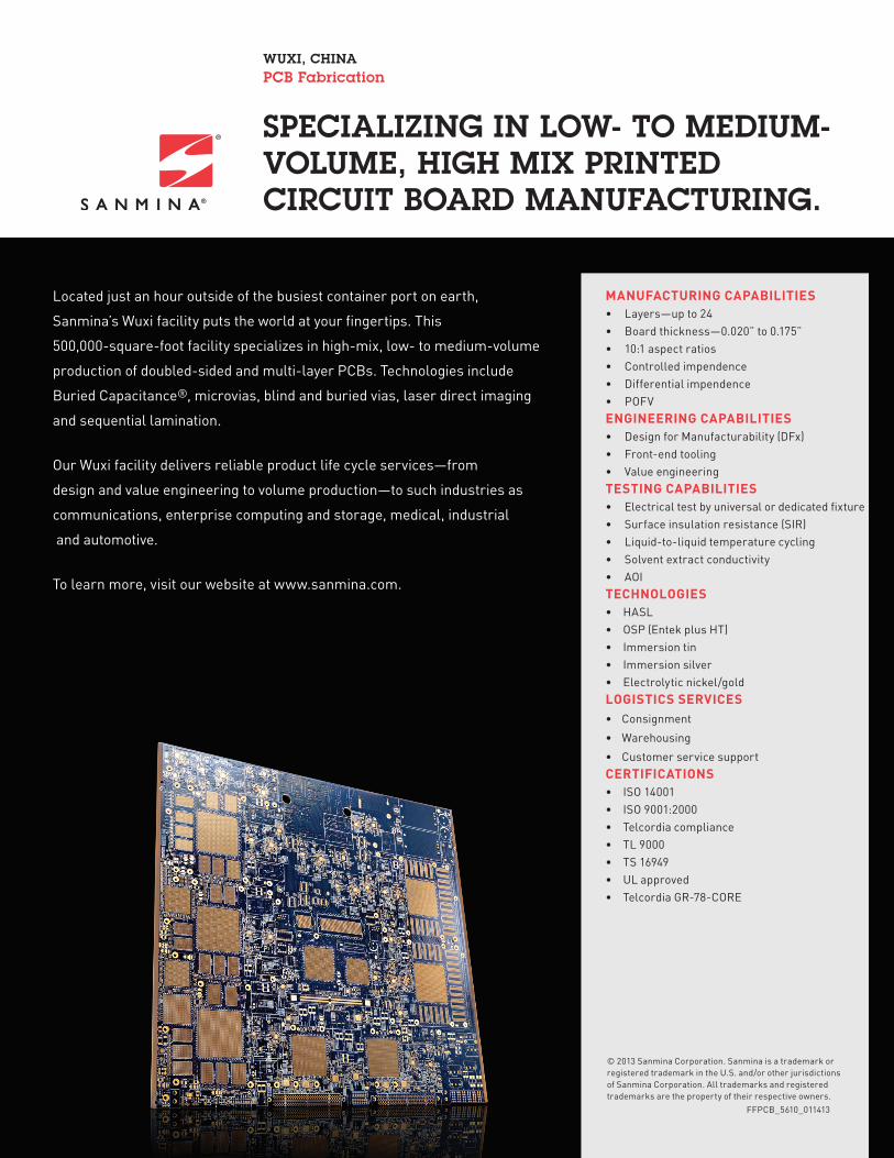
FFPCB_5610_011413 Located just an hour outside of the busiest container port on earth, Sanmina’s Wuxi facility puts the world at your fingertips. This 500,000-square-foot facility specializes in high-mix, low- to medium-volume production of doubled-sided and multi-layer PCBs. Technologies include Buried Capacitance ® , microvias, blind and buried vias, laser direct imaging and sequential lamination. Our Wuxi facility delivers reliable product life cycle services—from design and value engineering to volume production—to such industries as communications, enterprise computing and storage, medical, industrial and automotive. To learn more, visit our website at www.sanmina.com. SPECIALIZING IN LOW- TO MEDIUM- VOLUME, HIGH MIX PRINTED CIRCUIT BOARD MANUFACTURING. MANUFACTURING CAPABILITIES • Layers—up to 24 • Board thickness—0.020” to 0.175” • 10:1 aspect ratios • Controlled impendence • Differential impendence • POFV ENGINEERING CAPABILITIES • Design for Manufacturability (DFx) • Front-end tooling • Value engineering TESTING CAPABILITIES • Electrical test by universal or dedicated fixture • Surface insulation resistance (SIR) • Liquid-to-liquid temperature cycling • Solvent extract conductivity • AOI TECHNOLOGIES • HASL • OSP (Entek plus HT) • Immersion tin • Immersion silver • Electrolytic nickel/gold LOGISTICS SERVICES • Consignment • Warehousing • Customer service support CERTIFICATIONS • ISO 14001 • ISO 9001:2000 • Telcordia compliance • TL 9000 • TS 16949 • UL approved • Telcordia GR-78-CORE WUXI, CHINA PCB Fabrication © 2013 Sanmina Corporation. Sanmina is a trademark or registered trademark in the U.S. and/or other jurisdictions of Sanmina Corporation. All trademarks and registered trademarks are the property of their respective owners.