1663 MEMS/NEMS a 47. MEMS/NEMS and BioMEMS/BioNEMS: Materials, Devices, and Biomimetics Bharat Bhushan Micro-/nanoelectromechanical systems (MEMS/ NEMS) need to be designed to perform expected functions in short durations, typically in the mil- lisecond to picosecond range. The expected life of devices for high-speed contacts can vary from a few hundred thousand to many billions of cy- cles, e.g., over a hundred billion cycles for digital micromirror devices (DMDs), which puts serious requirements on materials. The surface-area-to- volume ratio in MEMS/NEMS is large, and in systems involving relative motion, surface forces such as adhesion, friction, and meniscus and viscous forces become very large compared with iner- tial and electromagnetic forces. There is a need for fundamental understanding of adhesion, fric- tion/stiction, wear, lubrication, and the role of surface contamination and environment, all on the nanoscale. Most mechanical properties are known to be scale dependent, therefore the prop- erties of nanoscale structures need to be measured. For bioMEMS/bioNEMS, adhesion between biologi- cal molecular layers and the substrate, and friction and wear of biological layers, can be important. Component-level studies are required to provide a better understanding of the tribological phe- nomena occurring in MEMS/NEMS. The emergence of the fields of nanotribology and nanomechanics, and atomic force microscopy (AFM)-based tech- niques, has provided researchers with a viable approach to address these problems. The emerging field of biomimetics holds promise for the de- velopment of biologically inspired nanomaterials and nanotechnology products. One example is the design of surfaces with roughness-induced super- hydrophobicity, self-cleaning, and low adhesion based on the so-called lotus effect. This chap- ter presents an overview of nanoscale adhesion, friction, and wear studies of materials and lubri- cation for MEMS/NEMS and bioMEMS/bioNEMS, and component-level studies of stiction phenomena in MEMS/NEMS devices, as well as hierarchical nano- structured surfaces for superhydrophobicity, self- cleaning, and low adhesion. 47.1 MEMS/NEMS Basics ................................ 1664 47.1.1 Introduction to MEMS .................. 1665 47.1.2 Introduction to NEMS ................... 1667 47.1.3 Introduction to BioMEMS/BioNEMS . 1668 47.1.4 Nanotribology and Nanomechanics Issues in MEMS/NEMS and BioMEMS/BioNEMS ................. 1668 47.2 Nanotribology and Nanomechanics Studies of Silicon and Related Materials ........................... 1683 47.2.1 Virgin and Treated/Coated Silicon Samples ..................................... 1684 47.2.2 Nanotribological and Nanomechanical Properties of Polysilicon Films and SiC Film.... 1689 47.3 Lubrication Studies for MEMS/NEMS ........ 1691 47.3.1 Perfluoropolyether Lubricants ....... 1691 47.3.2 Self-Assembled Monolayers (SAMs) 1694 47.3.3 Hard Diamond-Like Carbon (DLC) Coatings ..................................... 1697 47.4 Nanotribological Studies of Biological Molecules on Silicon-Based and Polymer Surfaces and Submicron Particles for Therapeutics and Diagnostics ........... 1698 47.4.1 Adhesion, Friction, and Wear of Biomolecules on Si-Based Surfaces 1698 47.4.2 Adhesion of Coated Polymer Surfaces ........... 1705 47.4.3 Submicron Particles for Therapeutics and Diagnostics ... 1706 47.5 Surfaces with Roughness-Induced Superhydrophobicity, Self-Cleaning, and Low Adhesion ................................ 1708 47.5.1 Modeling of Contact Angle for a Liquid Droplet in Contact with a Rough Surface................... 1710 Part H 47
Transcript
1663
MEMS/NEMS a47. MEMS/NEMS and BioMEMS/BioNEMS:Materials, Devices, and Biomimetics
Bharat Bhushan
Micro-/nanoelectromechanical systems (MEMS/NEMS) need to be designed to perform expectedfunctions in short durations, typically in the mil-lisecond to picosecond range. The expected lifeof devices for high-speed contacts can vary froma few hundred thousand to many billions of cy-cles, e.g., over a hundred billion cycles for digitalmicromirror devices (DMDs), which puts seriousrequirements on materials. The surface-area-to-volume ratio in MEMS/NEMS is large, and in systemsinvolving relative motion, surface forces such asadhesion, friction, and meniscus and viscousforces become very large compared with iner-tial and electromagnetic forces. There is a needfor fundamental understanding of adhesion, fric-tion/stiction, wear, lubrication, and the role ofsurface contamination and environment, all onthe nanoscale. Most mechanical properties areknown to be scale dependent, therefore the prop-erties of nanoscale structures need to be measured.For bioMEMS/bioNEMS, adhesion between biologi-cal molecular layers and the substrate, and frictionand wear of biological layers, can be important.Component-level studies are required to providea better understanding of the tribological phe-nomena occurring in MEMS/NEMS. The emergenceof the fields of nanotribology and nanomechanics,and atomic force microscopy (AFM)-based tech-niques, has provided researchers with a viableapproach to address these problems. The emergingfield of biomimetics holds promise for the de-velopment of biologically inspired nanomaterialsand nanotechnology products. One example is thedesign of surfaces with roughness-induced super-hydrophobicity, self-cleaning, and low adhesionbased on the so-called lotus effect. This chap-ter presents an overview of nanoscale adhesion,friction, and wear studies of materials and lubri-cation for MEMS/NEMS and bioMEMS/bioNEMS, andcomponent-level studies of stiction phenomena inMEMS/NEMS devices, as well as hierarchical nano-
structured surfaces for superhydrophobicity, self-cleaning, and low adhesion.
47.1 MEMS/NEMS Basics ................................ 166447.1.1 Introduction to MEMS .................. 166547.1.2 Introduction to NEMS ................... 166747.1.3 Introduction to BioMEMS/BioNEMS . 166847.1.4 Nanotribology and Nanomechanics
Issues in MEMS/NEMSand BioMEMS/BioNEMS ................. 1668
47.2 Nanotribology and NanomechanicsStudies of Siliconand Related Materials ........................... 168347.2.1 Virgin and Treated/Coated Silicon
47.4 Nanotribological Studies of BiologicalMolecules on Silicon-Basedand Polymer Surfacesand Submicron Particlesfor Therapeutics and Diagnostics ........... 169847.4.1 Adhesion, Friction, and Wear of
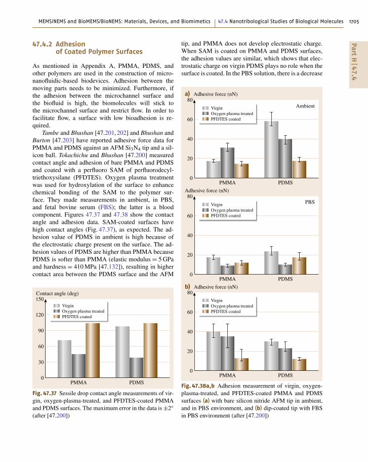
Biomolecules on Si-Based Surfaces 169847.4.2 Adhesion
of Coated Polymer Surfaces........... 170547.4.3 Submicron Particles
for Therapeutics and Diagnostics ... 1706
47.5 Surfaces with Roughness-InducedSuperhydrophobicity, Self-Cleaning,and Low Adhesion ................................ 170847.5.1 Modeling of Contact Angle
for a Liquid Droplet in Contactwith a Rough Surface................... 1710
PartH
47
1664 Part H Micro-/Nanodevice Reliability
47.5.2 Fabrication and Characterizationof Microstructures,Nanostructures,and Hierarchical Structures........... 1711
Microelectromechanical systems (MEMS) refer to mi-croscopic devices that have a characteristic length of< 1 mm but > 100 nm and that combine electrical andmechanical components. Nanoelectromechanical sys-tems (NEMS) refer to nanoscopic devices that havea characteristic length of < 100 nm and that combineelectrical and mechanical components. In mesoscale de-vices, if the functional components are on the micro-or nanoscale, they may be referred to as MEMS orNEMS, respectively. These are referred to as intelligentminiaturized systems comprising sensing, processing,and/or actuating functions and combining electricaland mechanical components. The acronym MEMSoriginated in the USA. The term commonly usedin Europe is microsystem technology (MST), and inJapan it is micromachines. Another term generallyused is micro-nanodevices. The terms MEMS/NEMSare also now used in a broad sense to includeelectrical, mechanical, fluidic, optical, and/or biolog-ical functions. MEMS/NEMS for optical applicationsare referred to as micro-/nanooptoelectromechanicalsystems (MOEMS/NOEMS). MEMS/NEMS for elec-tronic applications are referred to as radiofrequencyMEMS/NEMS (RF-MEMS/RF-NEMS). MEMS/NEMS for biological applications are referred to asbioMEMS/bioNEMS.
To put the characteristic dimensions and weightsof MEMS/NEMS and bioNEMS into perspective, seeFig. 47.1 and Table 47.1. NEMS and bioNEMS shownin the figure range in size from 2 to 300 nm, and thesize of MEMS is 12 000 nm. For comparison, individ-ual atoms are typically a fraction of a nanometer indiameter, deoxyribonucleic acid (DNA) molecules are
≈ 2.5 nm wide, biological cells are in the range of thou-sands of nm in diameter, and human hair is ≈ 75 μmin diameter. NEMS can be built with weight as low as10−20 N with cross sections of about 10 nm, and a mi-cromachined silicon structure can have a weight as lowas 1 nN. For comparison, the weight of a drop of wateris ≈ 10 μN and the weight of an eyelash is ≈ 100 nN.
Micro-nanofabrication techniques include top-downmethods, in which one builds down from the large tothe small, and bottom-up methods, in which one buildsup from the small to the large. Top-down methodsinclude micro-nanomachining methods and methodsbased on lithography as well as nonlithographic minia-turization, mostly for MEMS and fabrication of a fewNEMS devices. In bottom-up methods, also referred toas nanochemistry, devices and systems are assembledfrom their elemental constituents for NEMS fabrication,much as nature uses proteins and other macromoleculesto construct complex biological systems. The bottom-upapproach has the potential to go far beyond the limits oftop-down technology by producing nanoscale featuresthrough synthesis and subsequent assembly. Further-more, the bottom-up approach offers the potential toproduce structures with enhanced and/or completelynew functions. It allows a combination of materials withdistinct chemical composition, structure, and morphol-ogy. For a brief overview of fabrication techniques, seeAppendix A.
MEMS/NEMS and bioMEMS/bioNEMS are ex-pected to have a major impact on our lives, comparableto that of semiconductor technology, information tech-nology, or cellular and molecular biology [47.1–4]. They are used in electromechanical, electronics,
PartH
47.1
MEMS/NEMS and BioMEMS/BioNEMS: Materials, Devices, and Biomimetics 47.1 MEMS/NEMS Basics 1665
Size (nm)0.1 10 1001 1000 10 000 100 000
Human hair50–100μm
DMD12 µm
Red blood cell8 µm
Quantum-dot transistor300 nm
500 nm
Source Drain
Molecular gear10–100 nm
DNA2.5 nm
C atom0.16 nm
Mirror
Hinge
Yoke
Landingtip
MEMS: Characteristic length less than 1 mm,larger than 100 nm
NEMS: Less than 100 nm
SWNT chemical sensor2 nm
1 µm
SWNT
A
Fig. 47.1 Characteristic dimensions of MEMS/NEMS and bioNEMS in perspective. Examples shown are a single-walledcarbon nanotube (SWNT) chemical sensor [47.7], molecular dynamic simulations of carbon-nanotube-based gears [47.8],quantum-dot transistor obtained from van der Wiel et al. [47.9], and DMD (DLP Texas Instruments). For comparison,dimensions and weights of various biological objects found in nature are also presented
information/communication, chemical, and biologicalapplications. The MEMS industry in 2004 was worth≈ US$ 4.5 billion, with a projected annual growth rateof 17% [47.5]. Growth of Si-based MEMS is slow-ing down, while nonsilicon MEMS are picking up. TheNEMS industry was worth ≈ US$ 10 billion dollars in2004, mostly in nanomaterials [47.6]. It is expected toexpand in nanomaterials and biomedical applicationsas well as in nanoelectronics or molecular electronics.Due to the enabling nature of these systems and be-cause of the significant impact they can have on both
commercial and defense applications, industry as wellas federal governments have taken special interest inseeing growth nurtured in this field. MEMS/NEMS andbioMEMS/bioNEMS are the next logical step in thesilicon revolution.
47.1.1 Introduction to MEMS
The advances in silicon photolithographic process tech-nology since the 1960s led to the development ofMEMS in the early 1980s. More recently, lithographic
PartH
47.1
1666 Part H Micro-/Nanodevice Reliability
Table 47.1 Characteristic dimensions and weights in perspective
Characteristic dimensions in perspective
NEMS characteristic length < 100 nm
MEMS characteristic length < 1 mm and > 100 nm
Single-walled carbon nanotube (SWNT) chemical sensor ≈ 2 nm
Molecular gear ≈ 10 nm
Quantum-dot transistor 300 nm
Digital micromirror 12 000 nm
Individual atoms typically a fraction of a nm in diameter
DNA molecules ≈ 2.5 nm wide
Biological cells in the range of thousands of nm in diameter
Human hair ≈ 75 000 nm in diameter
Weights in perspective
NEMS built with cross-sections of ≈ 10 nm as low as 10−20 N
Micromachines, silicon structure as low as 1 nN
Eyelash ≈ 100 nN
Water droplet ≈ 10 μN
processes have also been developed to process non-silicon materials. Lithographic processes are beingcomplemented with nonlithographic processes for fab-rication of components or devices made from plastics orceramics. Using these fabrication processes, researchershave fabricated a wide variety of devices with di-mensions in the submicron range to a few thousandmicrons (see e.g., [47.10–20]). MEMS for mechan-ical applications include acceleration, pressure, flow,and gas sensors, linear and rotary actuators, and othermicrostructures or microcomponents such as electricmotors, gear chains, gas turbine engines, fluid pumps,fluid valves, switches, grippers, and tweezers. MEMSfor chemical applications include chemical sensors andvarious analytical instruments. MOEMS devices in-clude optical components, such as micromirror arraysfor displays, infrared image sensors, spectrometers,barcode readers, and optical switches. RF-MEMS in-clude inductors, capacitors, antennas, and RF switches.High-aspect-ratio MEMS (HARMEMS) have also beenintroduced.
A variety of MEMS devices have been producedand some are in commercial use [47.11, 13–16, 18–20].A variety of sensors are used in industrial, consumer,defense, and biomedical applications. The largest“killer” industrial applications include accelerome-ters, pressure sensors, thermal and piezoelectric inkjetprintheads, and digital micromirror devices. Integratedcapacitive-type silicon accelerometers have been usedin airbag deployment in automobiles since 1991 [47.21,22]; some 90 million units were installed in vehicles
in 2004. Accelerometer technology was over a billion-dollar-a-year industry in 2004, dominated by AnalogDevices followed by Freescale Semiconductor (for-merly Motorola) and Bosch. It is expected to grow withan annual growth exceeding 30%. Tri-axis accelerome-ters are needed to describe three-dimensional motion.Multi-axis accelerometers are being used for manyother applications such as vehicle stability, rollovercontrol, and gyro sensors for automotive applications,and various consumer applications including handhelddevices, e.g., laptops for free-fall detection (2003),cellular phones (2004), and personal digital assistants(PDAs) for menu navigation, gaming, image rotation,and free-fall detection. Silicon-based piezoresistivepressure sensors were launched in 1990 by GE No-vaSensor for manifold absolute pressure (MAP) sensingfor engines and for disposable blood-pressure sensors;their annual sales were more than 30 million units andmore than 25 million units, respectively, in 2004. MAPsensors measure the pressure in the intake manifold,which is fed to a computer that determines the opti-mum air–fuel mixture to maximize fuel economy. Mostvehicles have these as part of the electronic engine con-trol system. Capacitive pressure sensors for tire pressuremeasurements were launched by Freescale Semicon-ductor (formerly Motorola) in early 2000 and are alsomanufactured by Infineon/SensoNor and GE Novasen-sor (2003). Piezoresistive-type sensors are also used,manufactured by various companies such as EnTire So-lutions (2003). The sensing module is located insidethe rim of the wheel and relays the information via
PartH
47.1
MEMS/NEMS and BioMEMS/BioNEMS: Materials, Devices, and Biomimetics 47.1 MEMS/NEMS Basics 1667
radiofrequency to a central processing unit (CPU) in or-der to display it to the driver. In 2005, ≈ 9.2 millionvehicles were equipped with sensors, which trans-lated to ≈ 37 million units. Their sales have grownrapidly, as they are now required in automobiles inthe USA (starting in 2008), which affects 17 millionvehicles (with one device in each tire) sold everyyear. Pressure sensors can be used to detect altitudeby measuring air pressure. For example, global posi-tioning systems (GPS) used for navigation have goodlateral resolution but poor vertical resolution, whichcreates problems in identifying the level in the caseof multiple roads stacked up. A pressure sensor isneeded to determine the level (altitude) by measuringair pressure.
Thermal inkjet printers were developed indepen-dently by HP and Canon and commercialized in1984 [47.23–26] and today are made by Canon, Ep-son, HP, Lexmark, Xerox, and others. They typicallycost less initially than dry-toner laser printers and arethe solution of choice for low-volume print runs. An-nual sales of thermal inkjet printheads with microscalefunctional components were > 500 million units in2004.
Micromirror arrays are used for displays. Commer-cial digital light processing (DLP) equipment, usingdigital micromirror devices (DMD), were launched in1996 by Texas Instruments (TI) for digital projec-tion displays in computer projectors, high-definitiontelevision (HDTV) sets, and movie projectors (DLPcinema) [47.27–29]. Several million projectors hadbeen sold by 2004 (≈ US$ 700 million revenue by TIin 2004). Electrostatically actuated, membrane-typeor cantilever-type microswitches have been devel-oped for direct-current (DC), RF, and optical ap-plications [47.30]. There exists two basic forms ofRF microswitches: the metal-to-metal contact mi-croswitch (ohmic) and the capacitive microswitch. RFmicroswitches can be used in a variety of RF applica-tions, including cellular phones, phase shifters, smartantennas, multiplexers for data acquisition, etc. [47.31].Optical microswitches are finding applications in op-tical networking, telecommunications, and wirelesstechnologies [47.30, 32].
Other applications of MEMS devices include chem-ical/biological and gas sensors [47.20, 33], microres-onators, infrared detectors and focal-plane arrays forEarth observation, space science, and missile de-fense applications, picosatellites for space applications,fuel cells, and many hydraulic, pneumatic, and otherconsumer products. MEMS devices are also being pur-
sued in magnetic storage systems [47.34], where theyare being developed for supercompact and ultrahigh-recording-density magnetic disk drives. Several inte-grated head–suspension microdevices have been fab-ricated for contact recording applications [47.35].High-bandwidth servo-controlled microactuators havebeen fabricated for ultrahigh-track-density applications,where they serve as the fine-position control elementof a two-stage coarse–fine servo system, coupled witha conventional actuator [47.36, 37].
Micro-nanoinstruments and micro-nanomanipula-tors are used to move, position, probe, pattern, andcharacterize nanoscale objects and nanoscale fea-tures [47.38]. Miniaturized analytical equipments in-clude gas chromatography and mass spectrometry.Other instruments include micro-scanning tunnelingmicroscope (micro-STM).
In some cases, MEMS devices are used primar-ily for their miniature size, while in others, as in thecase of airbags, because of their low-cost manufactur-ing techniques. This latter fact has been possible sincesemiconductor processing costs have reduced drasti-cally over the last decade, allowing the use of MEMSin many fields.
47.1.2 Introduction to NEMS
NEMS are produced by nanomachining in a typicaltop-down approach (from large to small) and bottom-up approach (from small to large), largely relyingon nanochemistry (see, e.g., [47.39–45]). The NEMSfield, in addition to the fabrication of nanosystems,has provided impetus for the development of exper-imental and computation tools. Examples of NEMSinclude microcantilevers with integrated sharp nanotipsfor STM and atomic force microscopy (AFM) [47.46,47], quantum corrals formed using STM by placingatoms one by one [47.48], AFM cantilever arrays(millipede) for data storage [47.49], STM and AFMtips for nanolithography, dip-pen nanolithography forprinting molecules, nanowires, carbon nanotubes, quan-tum wires (QWRs), quantum boxes (QBs), quantumtransistors [47.9], nanotube-based sensors [47.50, 51],biological (DNA) motors, molecular gears formed byattaching benzene molecules to the outer walls of car-bon nanotubes [47.8], devices incorporating nm-thickfilms [e.g., in giant-magnetoresistive (GMR) read/writemagnetic heads and magnetic media for magnetic rigiddisk and magnetic tape drives], nanopatterned magneticrigid disks, and nanoparticles (e.g., nanoparticles inmagnetic tape substrates and nanomagnetic particles in
PartH
47.1
1668 Part H Micro-/Nanodevice Reliability
magnetic tape coatings) [47.34,52]. More than 2 billionread/write magnetic heads were shipped for magneticdisk and tape drives in 2004.
Nanoelectronics can be used to build computermemory using individual molecules or nanotubes tostore bits of information [47.53], molecular switches,molecular or nanotube transistors, nanotube flat-paneldisplays, nanotube integrated circuits, fast logic gates,switches, nanoscopic lasers, and nanotubes as elec-trodes in fuel cells.
47.1.3 Introduction to BioMEMS/BioNEMS
BioMEMS/bioNEMS are increasingly used in com-mercial and defense applications (see, e.g., [47.54–61]). They are used for chemical and biochemicalanalyses (biosensors) in medical diagnostics (e.g.,DNA, RNA, proteins, cells, blood pressure and assays,and toxin identification) [47.61, 62], tissue engineer-ing [47.63–65], and implantable pharmaceutical drugdelivery [47.66–68]. Biosensors, also referred to asbiochips, deal with liquids and gases. There are twotypes of biosensors. A large variety of biosensors arebased on micro-nanofluidics [47.61, 69–71]. Micro-nanofluidic devices offer the ability to work withsmaller reagent volumes and shorter reaction times, andperform analyses of multiple types at once. The secondtype of biosensors includes micro-nanoarrays whichperform one type of analysis thousands of times [47.72–75].
A chip, called lab-on-a-CD, with micro-nanofluidictechnology embedded on the disk can test thousands ofbiological samples rapidly and automatically [47.69].An entire laboratory can be integrated onto a singlechip, called a lab-on-a-chip [47.61, 70, 71]. Silicon-based disposable blood-pressure sensor chips wereintroduced in early 1990s by GE NovaSensor forblood-pressure monitoring (≈ 25 million units in 2004).A blood-sugar monitor, referred to as GlucoWatch, wasintroduced in 2002. It automatically checks blood sugarevery 10 min by detecting glucose through the skin,without having to draw blood. If glucose is out of the ac-ceptable range, it sounds an alarm so the diabetic patientcan address the problem quickly. A variety of biosen-sors, many using plastic substrates, are manufactured byvarious companies including ACLARA, Agilent Tech-nologies, Calipertech, and I-STAT.
The second type of biochips – micro-nanoarrays – isa tool used in biotechnology research to analyze DNAor proteins to diagnose diseases or discover new drugs.Also called DNA arrays, they can identify thousand of
genes simultaneously [47.57, 72]. They include a mi-croarray of silicon nanowires, roughly a few nm in size,to selectively bind and detect even a single biologicalmolecule such as DNA or protein by using nanoelec-tronics to detect the slight electrical charge caused bysuch binding, or a microarray of carbon nanotubes todetect glucose electrically.
After the tragedy of September 11, 2001, con-cern about biological and chemical warfare has ledto the development of handheld units with biologicaland chemical sensors for detection of biological germs,chemical or nerve agents, and mustard agents, and theirchemical precursors, to protect subways, airports, watersupplies, and the population at large [47.76].
BioMEMS/bioNEMS are also being developedfor minimally invasive surgery, including endoscopicsurgery, laser angioplasty, and microscopic surgery.Implantable artificial organs can also be produced.Other applications include: implantable drug-deliverydevices, e.g., micro-nanoparticles with drug moleculesencapsulated in functionalized shells for site-specifictargeting applications, and a silicon capsule witha nanoporous membrane filled with drugs for long-termdelivery [47.66, 77–79]; nanodevices for sequencingsingle molecules of DNA in the Human GenomeProject [47.61]; cellular growth using carbon nanotubesfor spinal-cord repair; nanotubes for nanostructured ma-terials for various applications such as spinal fusiondevices; organ growth; and growth of artificial tissuesusing nanofibers.
47.1.4 Nanotribology and NanomechanicsIssues in MEMS/NEMSand BioMEMS/BioNEMS
Tribological issues are important in MEMS/NEMS andbioMEMS/bioNEMS requiring intended and/or unin-tended relative motion. In these devices, various forcesassociated with the device scale down with the size.When the length of the machine decreases from 1 mm to1 μm, the surface area decreases by a factor of a million,and the volume decreases by a factor of a billion. Asa result, surface forces such as adhesion, friction, menis-cus forces, viscous forces, and surface tension that areproportional to surface area become a thousand timeslarger than the forces proportional to the volume, suchas inertial and electromagnetic forces. In addition tothe consequence of large surface-to-volume ratios, thesmall tolerances for which these devices are designedmake physical contacts more likely, thereby makingthem particularly vulnerable to adhesion between ad-
PartH
47.1
MEMS/NEMS and BioMEMS/BioNEMS: Materials, Devices, and Biomimetics 47.1 MEMS/NEMS Basics 1669
jacent components. Slight particulate or chemical con-tamination present at the interface can be detrimental.Furthermore, the small start-up forces and the torquesavailable to overcome retarding forces are small, and theincrease in resistive forces such as adhesion and fric-tion become a serious tribological concern that limitsthe durability and reliability of MEMS/NEMS [47.13].A large lateral force required to initiate relative motionbetween two surfaces, i.e., large static friction, is re-ferred to as stiction and has been studied extensivelyin the tribology of magnetic storage systems [47.34,46, 80–84]. The source of stiction is generally liquid-mediated adhesion, with the source of liquid beingprocess fluid or capillary condensation of water va-por from the environment. Adhesion, friction/stiction(static friction), wear, and surface contamination affectMEMS/NEMS and bioMEMS/bioNEMS performanceand, in some cases, can even prevent devices fromworking. Some examples of devices that experiencenanotribological problems follow.
Nanomechanical properties are scale dependent,therefore these should be measured at relevant scales.
MEMSFigure 47.2 shows examples of several microcompo-nents that can encounter the above-mentioned tribolog-ical problems. The polysilicon electrostatic micromotorhas 12 stators and a four-pole rotor and is producedby surface micromachining. The rotor diameter is120 μm, and the air gap between the rotor and stator is2 μm [47.85]. It is capable of continuous rotation at upto 100 000 rpm. The intermittent contact at the rotor–stator interface and physical contact at the rotor–hubflange interface result in wear issues, and high stic-tion between the contacting surfaces limits repeatabilityof operation or may even prevent operation altogether.Next, a bulk micromachined silicon stator–rotor pair isshown with a bladed rotor and nozzle guide vanes onthe stator with dimensions < 1 mm [47.86, 88]. Theseare being developed for a high-temperature micro gas-turbine engine with rotor dimension of 4–6 mm indiameter and operating speed of up to 1 million rpm(with a sliding velocity in excess of 500 m/s, compa-rable to velocities of large turbines operating at highvelocities) to achieve high specific power, up to a to-tal of ≈ 10 W. Erosion of blades and vanes and designof the microbearings required to operate at the ex-tremely high speeds used in the turbines are some of theconcerns. Ultrashort, high-speed micro hydrostatic gasjournal bearings with length-to-diameter ratio (L/D)of < 0.1 are being developed for operation at surface
2 mm
100 µm
a) b)
c) d)
100 µm
50 µm
Fig. 47.2a–d Examples of MEMS devices and components thatexperience tribological problems. (a) Electrostatic micromotor (af-ter [47.85]). (b) Microturbine bladed rotor and nozzle vanes onthe stator (after [47.86]). (c) Six-gear chain (Sandia). (d) Ni/FeWolfrom-type gear system produced by LIGA (after [47.87])
speeds of the order of 500 m/s, which results in uniquedesign challenges [47.89]. Microfabrica Inc. in the USAis developing microturbines with outer diameter as lowas 0.9 mm to be used as power sources for medicaldevices. They plan to use precision ball bearings.
Next in Fig. 47.2 is a scanning electron microscopy(SEM) micrograph of a surface-micromachined polysil-icon six-gear chain from Sandia National Lab. (Formore examples of an early version, see [47.90].)As an example of nonsilicon components, a mil-ligear system produced using the LIGA processfor a DC brushless permanent magnet millimotor(diameter = 1.9 mm, length = 5.5 mm) with an inte-grated milligear box [47.87, 91, 92] is also shown. Thegears are made of metal (electroplated Ni-Fe) but canalso be made from injected polymer materials (e.g.,polyoxy-methylene or POM) using the LIGA process.Even though the torque transmitted at the gear teeth issmall, of the order of a fraction of nN m, because of thesmall dimensions of gear teeth, the bending stresses arelarge where the teeth mesh. Tooth breakage and wear atthe contact of gear teeth is a concern.
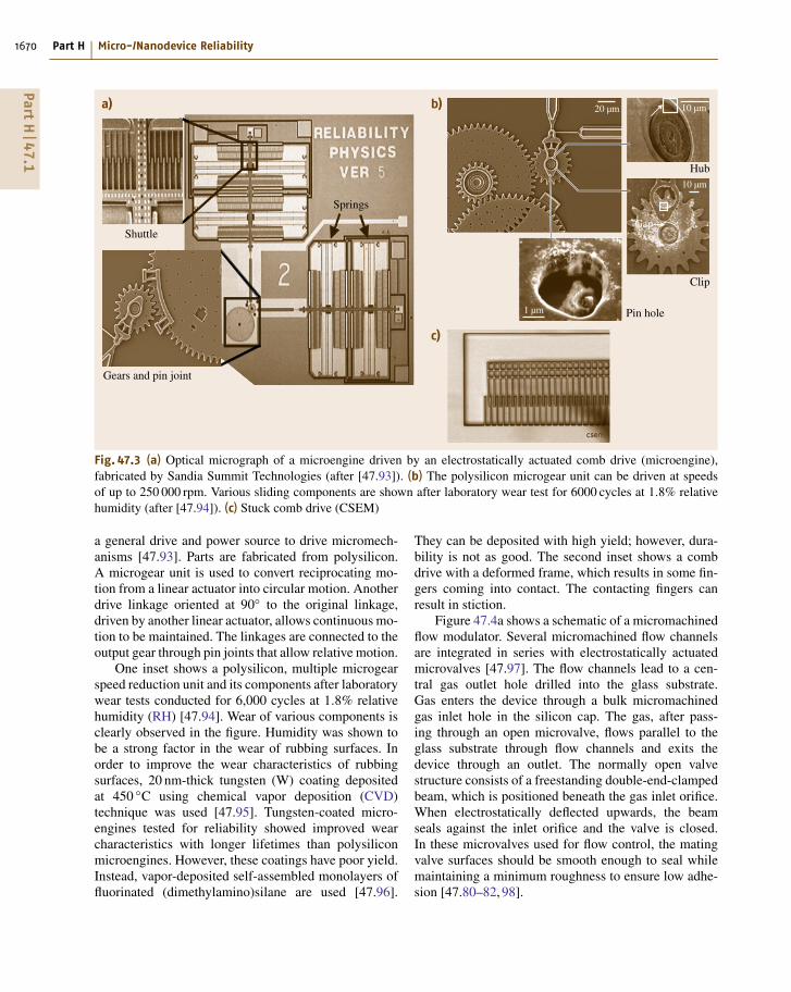
Figure 47.3 shows an optical micrograph of a mi-croengine driven by an electrostatically activated combdrive connected to the output gear by linkages, for oper-ation in the kHz frequency range, which can be used as
PartH
47.1
1670 Part H Micro-/Nanodevice Reliability
a)
1 µm Pin hole
Gears and pin joint
Shuttle
Springs
Clip
Hub
Gap
b)
c)
20 µm 10 µm
10 µm
Fig. 47.3 (a) Optical micrograph of a microengine driven by an electrostatically actuated comb drive (microengine),fabricated by Sandia Summit Technologies (after [47.93]). (b) The polysilicon microgear unit can be driven at speedsof up to 250 000 rpm. Various sliding components are shown after laboratory wear test for 6000 cycles at 1.8% relativehumidity (after [47.94]). (c) Stuck comb drive (CSEM)
a general drive and power source to drive micromech-anisms [47.93]. Parts are fabricated from polysilicon.A microgear unit is used to convert reciprocating mo-tion from a linear actuator into circular motion. Anotherdrive linkage oriented at 90◦ to the original linkage,driven by another linear actuator, allows continuous mo-tion to be maintained. The linkages are connected to theoutput gear through pin joints that allow relative motion.
One inset shows a polysilicon, multiple microgearspeed reduction unit and its components after laboratorywear tests conducted for 6,000 cycles at 1.8% relativehumidity (RH) [47.94]. Wear of various components isclearly observed in the figure. Humidity was shown tobe a strong factor in the wear of rubbing surfaces. Inorder to improve the wear characteristics of rubbingsurfaces, 20 nm-thick tungsten (W) coating depositedat 450 ◦C using chemical vapor deposition (CVD)technique was used [47.95]. Tungsten-coated micro-engines tested for reliability showed improved wearcharacteristics with longer lifetimes than polysiliconmicroengines. However, these coatings have poor yield.Instead, vapor-deposited self-assembled monolayers offluorinated (dimethylamino)silane are used [47.96].
They can be deposited with high yield; however, dura-bility is not as good. The second inset shows a combdrive with a deformed frame, which results in some fin-gers coming into contact. The contacting fingers canresult in stiction.
Figure 47.4a shows a schematic of a micromachinedflow modulator. Several micromachined flow channelsare integrated in series with electrostatically actuatedmicrovalves [47.97]. The flow channels lead to a cen-tral gas outlet hole drilled into the glass substrate.Gas enters the device through a bulk micromachinedgas inlet hole in the silicon cap. The gas, after pass-ing through an open microvalve, flows parallel to theglass substrate through flow channels and exits thedevice through an outlet. The normally open valvestructure consists of a freestanding double-end-clampedbeam, which is positioned beneath the gas inlet orifice.When electrostatically deflected upwards, the beamseals against the inlet orifice and the valve is closed.In these microvalves used for flow control, the matingvalve surfaces should be smooth enough to seal whilemaintaining a minimum roughness to ensure low adhe-sion [47.80–82, 98].
PartH
47.1
MEMS/NEMS and BioMEMS/BioNEMS: Materials, Devices, and Biomimetics 47.1 MEMS/NEMS Basics 1671
a)
b)
Siliconcap
Gasinlet
Beam Flowchannel
Pressuresensor
Gasoulet
Senseplate
Gasoulet
Metal pull-downplate
Slider
Spring
Suspension
Electrostaticactuator (nickel)
Siliconsubstrate
Fixed
Suspended
Fig. 47.4a,b Examples of MEMS devices that experiencetribological problems. (a) Low-pressure flow modulatorwith electrostatically actuated microvalves (after [47.97]).(b) Electroplated-nickel rotary microactuator for magneticdisc drives (after [47.37])
The second MEMS device shown (Fig. 47.4b) is anelectrostatically driven rotary microactuator for a mag-netic disk drive, surface-micromachined by a multilayerelectroplating method [47.37]. This high-bandwidthservo-controlled microactuator, located between a sliderand a suspension, is being developed for ultrahigh-track-density applications, which serves as the fine-position and high-bandwidth control element of a two-stage coarse–fine servo system when coupled witha conventional actuator [47.36, 37]. A slider is placedon top of the central block of a microactuator, whichprovides rotational motion to the slider. The bottomof the silicon substrate is attached to the suspen-sion. The radial flexure beams in the central blockgive rotational freedom of motion to the suspended
mass (slider), and the electrostatic actuator drives thesuspended mass. Actuation is accomplished via in-terdigitated, cantilevered electrode fingers, which arealternatingly attached to the central body of the mov-ing part and to the stationary substrate to form pairs.A voltage applied across these electrodes results inan electrostatic force which rotates the central block.The interelectrode gap width is ≈ 2 μm. Any unin-tended contacts between the moving and stationaryelectroplated-nickel electrodes may result in wear andstiction.
Commercially available MEMS devices also exhibittribological problems. Figure 47.5a shows an integratedcapacitive-type silicon accelerometer fabricated usingsurface micromachining by Analog Devices, a couple ofmm in dimension, which is used for airbag deploymentin automobiles, and more recently for various otherconsumer electronic markets [47.21, 99]. The centralsuspended beam mass (≈ 0.7 μg) is supported on thefour corners by spring structures. The central beam hasinterdigitated cantilevered electrode fingers (≈ 125 μmlong and 3 μm thick) on all four sides that alternatewith those of the stationary electrode fingers as shown,with about a 1.3 μm gap. Lateral motion of the centralbeam causes a change in the capacitance between theseelectrodes, which is used to measure the acceleration.Stiction between the adjacent electrodes as well as stic-tion of the beam structure with the underlying substrate,under isolated conditions, is detrimental to the opera-tion of the sensor [47.21, 99]. Wear during unintendedcontact of these polysilicon fingers is also a problem.A molecularly thick diphenyl siloxane lubricant film,resistant to high temperatures and oxidation, is appliedby a vapor-deposition process on the electrodes to re-duce stiction and wear [47.100]. For deposition, a smallamount of liquid is dispensed into each package beforeit is sealed. As the package is heated in the furnace,the liquid evaporates and coats the sensor surface. Assensors are required to sense low-g accelerations, theyneed to be more compliant and stiction becomes an evenbigger concern.
Figure 47.5b shows a cross-sectional view of a typ-ical piezoresistive-type pressure sensor, which is usedfor various applications including manifold absolutepressure (MAP) and tire pressure measurements in au-tomotive applications, and disposable blood-pressuremeasurements. The sensing material is a diaphragmformed on a silicon substrate, which bends with ap-plied pressure [47.101, 102]. The deformation causesa change in the band structure of the piezoresistors thatare placed on the diaphragm, leading to a change in the
PartH
47.1
1672 Part H Micro-/Nanodevice Reliability
Sensingdiaphragm
Protective polymer gel
Die-attach polymer adhesive
Print plane
Nozzle layer
Refill region Bubble
Barrier layer
To intimateelectronics
Heater
Si heater substrateInk
To ink supply
Applied pressure
Supportingsprings
Suspendedmass
Stationaryplates
Suspendedmass
Stationaryplates
a) b)
c)
Fig. 47.5a–c Examples of MEMS devices in commercial use that experience tribological problems. (a) Capacitive-type silicon accelerometer for automotive sensory applications (after [47.99]). (b) Piezoresistive-type pressure sensor(after [47.102]). (c) Thermal inkjet printhead (after [47.25])
resistivity of the material. MAP sensors are subjected todrastic conditions – extreme temperatures, vibrations,sensing fluid, and thermal shock. Fluid under extremeconditions could cause corrosive wear. Fluid cavitationcould cause erosive wear. The protective gel encapsu-lant generally used can react with the sensing fluid andresult in swelling or dissolution of the gel. Silicon can-not deform plastically, therefore any pressure spikesleading to deformation past its elastic limit will resultin fracture and crack propagation. Pressure spikes couldalso cause the diaphragm to delaminate from the sup-port substrate. Finally, cyclic loading of the diaphragmduring use can lead to fatigue and wear of the silicondiaphragm or delamination.
The schematic in Fig. 47.5c shows a cross-sectionalview of a thermal printhead chip (of the order of10–50 cm3 in volume) used in inkjet printers [47.25].They comprise an ink supply and an array of elementswith microscopic heating resistors on a substrate matedto a matching array of injection orifices or nozzles(≈ 70 μm in diameter) [47.23, 24, 26]. In each element,a small chamber is heated by the resistor, where a briefelectrical impulse vaporizes part of the ink and cre-
ates a tiny bubble. The heaters operate at several kHzand are therefore capable of high-speed printing. Asthe bubble expands, some of the ink is pushed outof the nozzle onto the paper. When the bubble pops,a vacuum is created and this causes more ink fromthe cartridge to move into the printhead. Clogged inkports are the major failure mode. There are varioustribological concerns [47.23]. The surface of the print-head from where the ink is ejected towards the papercan become scratched or damaged as a result of count-less trips back and forth across the pages, which aresomewhat rough. As a result of repeated heating andcooling, the heated resistors expand and contract. Overtime, these elements will experience fatigue and mayeventually fail. Bubble formation in the ink reservoircan lead to cavitation erosion of the chamber, whichoccurs when bubbles formed in the fluid become un-stable and implode against the surface of the solidand impose impact energy on that surface. Fluid flowthrough nozzles may cause erosion and ink particlesmay also cause abrasive wear. Corrosion of the inkreservoir surfaces can also occur as a result of expo-sure of ink to high temperatures as well as due to
PartH
47.1
MEMS/NEMS and BioMEMS/BioNEMS: Materials, Devices, and Biomimetics 47.1 MEMS/NEMS Basics 1673
ink pH. The substrate of the chip consists of siliconwith a thermal barrier layer followed by a thin filmof resistive material and then conducting material. Theconductor and resister layers are generally protected byan overcoat layer of a plasma-enhanced chemical va-por deposition (PECVD) α-SiC:H layer, 200–500 nmthick [47.103].
Figure 47.6a shows two digital micromirror device(DMD) pixels used in digital light processing (DLP)technology for digital projection displays in computerprojectors, high-definition television (HDTV) sets, andmovie projectors [47.27–29]. The entire array (chip set)consists of a large number of oscillating aluminum al-loy micromirrors as digital light switches which are
fabricated on top of a complementary metal–oxide–semiconductor (CMOS) static random-access memoryintegrated circuit. The surface-micromachined arrayconsists of half a million to more than two millionof these independently controlled reflective micromir-rors, each ≈ 12 μm square and with 13 μm pitch, whichflip backward and forward at a frequency of of theorder of 5000–7000 times a second as a result of elec-trostatic attraction between the micromirror structureand the underlying electrodes. For binary operation,the micromirror–yoke structure mounted on torsionalhinges is oscillated ±10◦ (with respect to the planeof the chip set), limited by a mechanical stop. Con-tact between cantilevered spring tips at the end of the
PartH
47.1
1674 Part H Micro-/Nanodevice Reliability
yoke (four present on each yoke) and the underly-ing stationary landing sites is required for true digital(binary) operation. Stiction and wear during contactbetween aluminum-alloy spring tips and landing sites,hinge memory (metal creep at high operating temper-atures), hinge fatigue, shock and vibration failure, andsensitivity to particles in the chip package and operatingenvironment are some of the important issues affectingthe reliable operation of a micromirror device [47.105–109]. A vapor-phase-deposited self-assembled mono-layer of the fatty acid perfluorodecanoic acid (PFDA)on surfaces of the tip and landing sites is used to re-duce stiction and wear [47.110, 111]. However, thesefilms are susceptible to moisture, and to keep moistureout and create a background pressure of PFDA, a her-metic chip package is used. The spring tip is used inorder to use the stored spring energy to pop up the tipduring pull-off. A lifetime estimate of over 100 000 hoperation with no degradation in image quality is thenorm. At a mirror modulation frequency of 7 kHz,each micromirror element needs to switch ≈ 2.5 trillioncycles.
Figure 47.6b shows a schematic of a 256 × 256-port large optical cross-connect, introduced in 2000 byGlimmerglass (Hayward, CA) for optical telecommu-nication networks in order to be able to manipulatea larger number of optical signals rapidly [47.104]. Thisoptical microswitch uses 256 or more movable mirrorson a chip for switching a light beam from an inputfiber to a few output fibers. The mirrors are made ofgold-coated polysilicon and are ≈ 500 μm in diameter.Reliability concerns are the same as those describedabove for DMDs. To minimize stiction, the chipset ishermetically sealed in dry nitrogen (90% N2, 10% He).
Figure 47.6c shows a schematic of an elec-trostatically-actuated capacitive-type RF microswitchfor switching of RF signals at microwave and low fre-quencies [47.112]. It is of membrane type and consistsof a flexible metal (Al) bridge that spans the RF trans-mission line in the center of a coplanar waveguide.When the bridge is up, the capacitance between thebridge and RF transmission line is small, and the RFsignal passes without much loss. When a DC voltageis applied between the RF transmission line and thebridge, the latter is pulled down until it touches a dielec-tric isolation layer. The large capacitance thus createdshorts the RF signal to ground. The failure modes in-clude creep in the metal bridge, fatigue of the bridge,charging and degradation of the dielectric insulator, andstiction of the bridge to the insulator [47.30, 112]. Stic-tion occurs due to capillary condensation of water vapor
from the environment, van der Waals forces, and/orcharging effects. If the restoring force in the bridge ofthe switch is not large enough to pull the bridge upagain after the actuation voltage has been removed, thedevice fails due to stiction. Humidity-induced stictioncan be avoided by hermetically sealing the microswitch.Some roughness of the surfaces reduces the probabilityof stiction. Selected actuation waveforms can be used tominimize charging effects.
NEMSProbe-based data recording technologies are being de-veloped for ultrahigh-areal-density recording, wherethe probe tip is expected to be scanned at veloci-ties up to 100 mm/s. There are three major techniquesbeing developed: thermomechanical [47.49], phasechange [47.113], and ferroelectric recording [47.114,115]. We discuss the tribological issues with two of thewidely pursued techniques [47.116].
Figure 47.7a shows the thermomechanical record-ing system which uses arrays of 1,024 silicon micro-cantilevers and playback on an ≈ 40 nm-thick polymermedium with a harder Si substrate [47.49]. The can-tilevers consist of integrated tip heaters with tips ofnanoscale dimensions. (The sharp tips themselves arealso example of NEMS.) Thermomechanical recordingis a combination of applying a local force to the polymerlayer and softening it by local heating. The tip, heatedto ≈ 400 ◦C, is brought into contact with the polymerfor recording. Readings are done using the cantileverheater, originally used for recording, as a thermal read-back sensor by exploiting its temperature-dependentresistance. The principle of thermal sensing is based onthe fact that the thermal conductivity between the heaterand the storage substrate changes according to the spac-ing between them. When the spacing between the heaterand sample is reduced as the tip moves into a bit,the heater’s temperature and hence its resistance willdecrease. Thus, changes in temperature of the continu-ously heated resistor are monitored while the cantileveris scanned over data bits, providing a means of detect-ing the bits. Erasing for subsequent rewriting is carriedout by thermal reflow of the storage field by heating themedium to 150 ◦C for a few seconds. The smoothnessof the reflown medium allows multiple rewriting of thesame storage field. Bit sizes ranging between 10 and50 nm have been achieved by using a 32 × 32 (1,024) ar-ray write/read chip (3 mm × 3 mm). It has been reportedthat tip wear occurs due to contact between tip and Sisubstrate during writing. Tip wear is considered a majorconcern for the device reliability.
PartH
47.1
MEMS/NEMS and BioMEMS/BioNEMS: Materials, Devices, and Biomimetics 47.1 MEMS/NEMS Basics 1675
Millipede concept32 × 32 tip array
Writing by applying DC voltage in contact mode
AFM cantileverPolarized regions
DCVPZT
SrRuO3Current
SrTiO3
Single tip
b)
a)
Reading of piezoelectric response in contactor electrostatic force in noncontact mode byappling AC voltage
ACVPZTPZT
AFM tip
SrRuO3
SrRuO3
Electrostaticinteraction
SrTiO3
Fig. 47.7a,b Two example of NEMS devices: (a) thermomechanical recording, and (b) ferroelectric recording, whichexperience tribological problems
Figure 47.7b shows a schematic of domain writ-ing and reading in a ferroelectric film. The electricallyconductive AFM tips are placed in contact witha piezoelectric (lead zirconate titanate, PZT) film-coated medium [47.114, 115]. Ferroelectric domains onthe PZT film are polarized by applying short voltagepulses (≈ 10 V, ≈ 100 μs) that exceed the coercive fieldof the PZT layer, resulting in local, nonvolatile changesin the electronic properties of the underlying film. Thetemperature rise during recording is expected to be ofthe order of 80 ◦C. Reading out of the polarization statesin the ferroelectric film can be carried out using two dif-ferent methods. In one method, the static surface charge,proportional to the normal component of polarization,can be detected by electrostatic force microscopy in thenoncontact mode. In the second method, an AFM is op-erated in contact mode and the piezoresponse force ismeasured by applying an alternating-current (AC) volt-age. Wear of the conducting tip and the PZT layer athigh scanning velocities is a major concern for devicereliability. Various lubricant films are being developedto minimize wear [47.113–119].
In magnetic data storage, magnetic recording isaccomplished by relative motion between the mag-netic head slider and a magnetic rigid disk [47.34].
Magnetic rigid disks and heads used today for mag-netic data storage consist of nanostructured films a fewnm thick. Figure 47.8a shows a sectional view ofa conventional multigrain magnetic rigid disk. The su-perparamagnetic effect poses a serious challenge for theever-increasing areal density of disk drives. One of thepromising methods to circumvent the density limita-tions imposed by this effect is the use of a nanopatterneddisk (Fig. 47.8b). In a conventional disk, the thin mag-netic layer forms a random mosaic of nanometer-scalegrains, and each recorded bit consists of many tensof these random grains. In a patterned disk, the mag-netic layer is created as an ordered array of highlyuniform islands, each island capable of storing an indi-vidual bit. These islands may be one or a few grains,rather than a collection of random decoupled grains.This increases the density by a couple of orders ofmagnitude. Figure 47.8c shows a schematic of an in-ductive write/giant-magnetoresistive (GMR) read headstructure. These are constructed from a variety of ma-terials: magnetic alloys, metal conductors, ceramic,and polymer insulators in a complex three-dimensionalstructure. The multilayered thin-film structure used toconstruct the sensor and individual films are only a fewnm thick. The head slider surface, which flies over the
Fig. 47.8a–c Schematic of (a) sectional view of a conven-tional multigrain magnetic rigid disk, (b) nanopatternedmagnetic rigid disk, and (c) an inductive write/GMR readmagnetic head structure for magnetic data storage (Hitachi)
disk surface, is coated with ≈ 3 nm-thick diamond-likecarbon coatings to protect the thin-film structure fromelectrostatic discharge. Any isolated contacts betweenthe disk and sensor and lubricant pickup pose tribologi-cal concerns [47.34].
BioMEMSAn example of a wristwatch-type biosensor basedon microfluidics, referred to as a lab-on-a-chip sys-
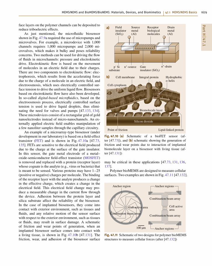
tem, is shown in Fig. 47.9a [47.61, 70]. These systemsare designed either to detect a single or a class of(bio)chemicals or for system-level analytical capabili-ties for a broad range of (bio)chemical species (knownas a micro total analysis system, mTAS), and have theadvantage of incorporating sample handling, separa-tion, detection, and data analysis onto one platform.The chip relies on microfluidics and involves manipu-lation of tiny amounts of fluids in microchannels usingmicrovalves. The test fluid is injected into the chip, gen-erally using an external pump or syringe, for analysis.Some chips have been designed with an integrated elec-trostatically actuated diaphragm-type micropump. Thesample, which can have volume measured in nanoliters,flows through microfluidic channels via an electric po-tential and capillary action using microvalves (havingvarious designs, including membrane type) for variousanalyses. The fluid is preprocessed and then analyzedusing a biosensor. Another example of a biosensor isthe cassette-type biosensor used for human genomicDNA analysis; integrated biological sample prepara-tion is shown in Fig. 47.9b [47.71]. The implementationof micropumps and microvalves allows for fluid ma-nipulation and multiple sample processing steps ina single cassette. Blood or other aqueous solutions canbe pumped into the system, where various processes areperformed.
Microvalves, which are found in most microfluidiccomponents of bioMEMS, can be classified in two cat-egories: active microvalves (with an actuator) for flowregulation in microchannels and passive microvalvesintegrated with micropumps. Active microvalves con-sist of a valve seat and a diaphragm actuated byan external actuator [47.62, 120, 121]. Different typesof actuators are based on piezoelectric, electrostatic,thermopneumatic, electromagnetic, and bimetallic ma-terials, shaped-memory alloys, and solenoid plungers.An example of an electrostatic cantilever-type activemicrovalve is shown in Fig. 47.9c [47.120]. Passivemicrovalves used in micropumps include mechanicalcheck valves and a diffuser/nozzle [47.62, 121–124].Check valves consist of a flap or membrane that iscapable of opening and closing with changes in pres-sure; see Fig. 47.9c for schematics. A diffuser/nozzleuses an entirely different principle and only works withthe presence of a reciprocating diaphragm. When oneconvergent channel works simultaneously with anotherconvergent channel oriented in a specific direction,a change in pressure is possible.
There are four main types of mechanical microp-umps, which include a diaphragm micropump that
PartH
47.1
MEMS/NEMS and BioMEMS/BioNEMS: Materials, Devices, and Biomimetics 47.1 MEMS/NEMS Basics 1677
70–80 µm
Magnetic beadswith dendrimer
Biofilter with immunosensor Microvalve
Control system and circuits
Flow sensor
Embeddedbiofluidicchips
75 mm
a) Lab-on-a-chip
b) Cassette type Wash Valve Filter region Elution chamber
Elution pump
PCR reaction tube
Post-PCR outlet
Post-PCR pumpWasteFilter pump
Sample
Fig. 47.9 (a) MEMS-based biofluidic chip, commonly known as a lab-on-a-chip, that can be worn like a wristwatch(after [47.70]). (b) Cassette-type biosensor used for human genomic DNA analysis (after [47.71]). PCR, polymerasechain reaction
involves mechanical check valves, valveless rectifi-cation pumps that use diffuser/nozzle type valves,valveless pumps without a diffuser/nozzle, electro-static micropumps, and rotary micropumps [47.62,121–124]. Diaphragm micropumps consist of a reciprocat-ing diaphragm which can be piezoelectrically driven,working in synchronization with two check valves(Fig. 47.9c) [47.123]. Electrostatic micropumps havea diaphragm as well, but it is driven using two electrodes(Fig. 47.9c) [47.125]. Valveless micropumps also con-sist of a diaphragm, which is piezoelectrically driven,but do not incorporate passive mechanical valves. In-
stead, these pumps use an elastic buffer or variable-gapmechanism. Finally, a rotary micropump has a rotatingrotor that simply adds momentum to the fluid by the fastmoving action of the blades (Fig. 47.9c) [47.126, 127].Rotary micropumps can be driven using an integratedelectromagnetic motor or by the presence of an externalelectric field. All of these micropumps can be made ofsilicon or a polymer material.
During the operation of the microvalves and microp-umps discussed above, adhesion and friction propertiesbecome important when contacts occur due to rel-ative motion. During operation, active mechanical
PartH
47.1
1678 Part H Micro-/Nanodevice Reliability
c) Active electrostatic microvalve
Electrode plates
Dielectric
Base plate Silicon
Exhaust
Inlet orifice
Passive mechanical check valves
Valveless micropump
Valve 1 Valve 2 Diaphragm Piezodisk
Diaphragm micropump
Inlet Outlet
Piezo discPiezo bimorph cantilever
Membrane valveFlap valve
Inlet
SpacerMembrane
Outlet
Pressure chamber
Upperelectrode
Lowerelectrode
Electrostatic micropump
Rotary micropump
(after [49.119])
(after [49.122])
(after [49.124])
(after [49.121]) (after [49.123])
(after [49.119])
(after [49.125])
(after [49.126])
Closure plate
Fig. 47.9 (c) Multiple examples of valves and pumps found in bioMEMS devices. Mechanical check valves, diaphragmmicropump, valveless micropump, and rotary micropump
microvalves have an externally actuated diaphragmwhich comes into contact with a valve seat to restrictfluid flow. Adhesion between the diaphragm and valveseat will affect the operation of the microvalve. In thediaphragm micropumps, two passive mechanical checkvalves are incorporated into the design. Passive mechan-ical check valves also exhibit adhesion when the flap ormembrane comes into contact with the valve seat whenfluid flow is prevented. Adhesion also occurs duringthe operation of valveless micropumps when the di-aphragm, which is piezoelectrically driven, comes intocontact with the rigid outlet. Finally, adhesion and fric-
tion can also be seen during the operation of rotarymicropumps when the gears rotate and come into con-tact and rub against one another.
If the adhesion between the microchannel surfaceand the biofluid is high, biomolecules will stick to themicrochannel surface and restrict flow. In order to facil-itate flow, microchannel surfaces with low bioadhesionare required. Fluid flow in polymer channels can pro-duce triboelectric surface potential, which may affectthe flow. Polymers are known to generate surface po-tential, and the magnitude of the potential varies fromone polymer to another [47.128–130]. Conductive sur-
PartH
47.1
MEMS/NEMS and BioMEMS/BioNEMS: Materials, Devices, and Biomimetics 47.1 MEMS/NEMS Basics 1679
face layers on the polymer channels can be deposited toreduce triboelectric effects.
As just mentioned, the microfluidic biosensorshown in Fig. 47.9a required the use of micropumps andmicrovalves. For example, a microdevice with 1,000channels requires 1,000 micropumps and 2,000 mi-crovalves, which makes it bulky and poses reliabilityconcerns. Two methods can be used for driving the flowof fluids in microchannels: pressure and electrokineticdrive. Electrokinetic flow is based on the movementof molecules in an electric field due to their charges.There are two components to electrokinetic flow: elec-trophoresis, which results from the accelerating forcedue to the charge of a molecule in an electric field, andelectroosmosis, which uses electrically controlled sur-face tension to drive the uniform liquid flow. Biosensorsbased on electrokinetic flow have also been developed.In so-called digital-based microfluidics, based on theelectroosmosis process, electrically controlled surfacetension is used to drive liquid droplets, thus elimi-nating the need for valves and pumps [47.133, 134].These microdevices consist of a rectangular grid of goldnanoelectrodes instead of micro-nanochannels. An ex-ternally applied electric field enables manipulation ofa few nanoliter samples through the capillary circuitry.
An example of a microarray-type biosensor (underdevelopment in our laboratory) is based on a field-effecttransistor (FET) and is shown in Fig. 47.10a [47.73,135]. FETs are sensitive to the electrical field produceddue to the charge at the surface of the gate insulator.In this sensor, the gate metal electrode of a metal–oxide-semiconductor field-effect transistor (MOSFET)is removed and replaced with a protein (receptor layer)whose cognate is the analyte (e.g., virus or bacteria) thatis meant to be sensed. Various proteins may have 1–25(positive or negative) charges per molecule. The bindingof the receptor layer with the analyte produces a changein the effective charge, which creates a change in theelectrical field. This electrical field change may pro-duce a measurable change in the current flow throughthe device. Adhesion between the protein layer andsilica substrate affect the reliability of the biosensor.In the case of implanted biosensors, they come intocontact with exterior environment, such as tissues andfluids, and any relative motion of the sensor surfacewith respect to the exterior environment, such as tissuesor fluids, may result in surface damage. A schematicof friction and wear points of generation, when animplanted biosensor surface comes into contact witha living tissue, is shown in Fig. 47.10b [47.131]. Thefriction, wear, and adhesion of the biosensor surface
a) Fieldinsulator(SiO2)
Sourcemetal(Al)
Receptorbiologicalmolecules
Drainmetal(Al)
p– Sisubstrate
n+-source Gateinsulator (SiO2)
n+-drain
b)
Point of friction
Silicon dioxide
Biomolecule layer
Cell cytoplasm
Cell membrane Integral protein Hydrophobicα helix
Lipid-linked protein
Fig. 47.10 (a) Schematic of a bioFET sensor (af-ter [47.73]), and (b) schematic showing the generation offriction and wear points due to interaction of implantedbiomolecule layer on a biosensor with living tissue (af-ter [47.131])
may be critical in these applications [47.73, 131, 136,137].
Polymer bioMEMS are designed to measure cellularsurfaces. Two examples are shown in Fig. 47.11 [47.132].
Anchor region
Cell active area
Combination beam array
Anchor regions
Combination beam array
Cell activearea
Combination beam array
Anchor regions100 µm
Fig. 47.11 Schematic of two designs for polymer bioMEMSstructures to measure cellular forces (after [47.132])
PartH
47.1
1680 Part H Micro-/Nanodevice Reliability
The device on the left shows cantilevers anchored at theperiphery of the circular structure, while the device onthe right has cantilevers anchored at the two corners onthe top and the bottom. The cell adheres to the centerof the structure, and the contractile forces generated inthe cell’s cytoskeleton cause the cantilever to deflect.The deflection of the compliant polymer cantilevers ismeasured optically and related to the magnitude of theforces generated by the cell. Adhesion between cellsand the polymer beam is desirable. In order to design thesensors, micro- and nanoscale mechanical properties ofpolymer structures are needed.
BioNEMSMicro-nanofluidic devices provide a powerful plat-form for electrophoretic separations for a variety ofbiochemical and chemical analysis. Electrophoresis isa versatile analytical method which is used for sep-aration of small ions, neutral molecules, and largebiomolecules. Figure 47.12 shows an interdigitatedmicro-nanofluidic silicon array with nanochannels fora separation process. Figure 47.13a shows a schematicof an implantable, immunoisolation submicroscopic
Nanochannels for separation process
Interdigitated micro-/nanofluidic array
Micro-channels
Nano-channel
Exploded view of silicon nanochannels
50 µm
1 µm
Fig. 47.12 Interdigitated micro-nanofluidic silicon arrayfor a separation process (after [47.135, 138])
biocapsule, aimed at drug delivery in order to treatsignificant medical conditions such as type I dia-betes [47.77, 78]. The purpose of the immunoisolationbiocapsule is to create an implantable device capable ofsupporting foreign living cells that can be transplantedinto humans. It is a silicon capsule consisting of twonanofabricated membranes bonded together with thedrug (e.g., encapsulated insulin-producing islet cells)contained within the cavities for long-term delivery. Thepores or nanochannels in a semipermeable membrane assmall as 6 nm are used as flux regulators for long-termrelease of drugs. The nanomembrane also protects ther-apeutic substances from attack by the body’s immunesystem. The pores are large enough to provide the flowof nutrients (e.g., glucose molecules) and drug (e.g.,insulin), but small enough to block natural antibodies.Antibodies have the capability to penetrate any orifice> 18 nm. The 50 nm pores in silicon were etched by us-ing sacrificial-layer lithography, described in AppendixA [47.78].
The main reliability concerns in the micro-nanoflui-dic silicon array and implantable biocapsules arebiocompatibility and potential biofouling (undesir-able accumulation of microorganisms) of the chan-nels/membrane due to protein and cell adsorption frombiological fluids. Biofouling can also result in cloggingof the nanochannels/nanopores, which could potentiallyrender the device ineffective. The adhesion of pro-teins and cells to an implanted device can also causedetrimental results such as inflammation and excessivefibrosis. Deposition of self-assembled monolayers ofselected organic molecules onto the channels of theimplants, which makes them hydrophobic, presents aninnovative solution to combat the adverse effects of bi-ological fluids [47.138–141].
Figure 47.13b shows a conceptual model of anintravascular drug-delivery device: nanoparticles usedto search and destroy disease (tumor) cells [47.79].(The tumor cells have one or two orders of magni-tude higher density of receptors than normal cells andlower pH. Some receptors are only expressed on tu-mor cells.) With lateral dimensions of 1 μm or less, theparticles are smaller than any blood cells. These par-ticles can be injected into the blood stream and travelfreely through the circulatory system. In order to di-rect these drug-delivery nanoparticles to cancer sites,their external surfaces are chemically modified to carrymolecules that have lock-and-key binding specificitywith molecules that support a growing cancer mass.As the particles come into close proximity with dis-eased cells, the ligands on the particle surfaces attach
PartH
47.1
MEMS/NEMS and BioMEMS/BioNEMS: Materials, Devices, and Biomimetics 47.1 MEMS/NEMS Basics 1681
Fig. 47.13a,b Schematics of (a) implantable, immunoisolation submicroscopic biocapsules (drug-delivery device) (af-ter [47.78]), and (b) intravascular nanoparticles for search and destroy of diseased blood cells (after [47.79])
to the receptors on the cells. As soon as the particlesdock onto the cells, a compound is released that formsa pore on the membrane of the cells, which leads tocell death and ultimately to that of the cancer massthat was being nourished by the blood vessel. Theadhesive interactions are regulated by specific (ligand–receptor binding) and nonspecific (short-range van derWaals, electrostatic, and steric) interactions [47.142].Adhesion between nanoparticles and disease cells is re-quired. Furthermore, the particles should travel closeto the endothelium lining of vascular arteries to facil-itate the interaction between the particles and diseasedcells. Decuzzi et al. [47.142] analyzed the marginationof a particle circulating in the blood stream and cal-culated the speed and time for margination (driftingof particles towards the blood vessel walls) as a func-tion of the density and diameter of the particle, basedon various forces present between the circulating par-ticle and the endothelium lining. Human capillaries
can have radii as small as 4–5 μm. They reported thatparticles used for drug delivery should have a radiussmaller than a critical value in the range of 100 nm.
SiO2/Si
Pd/AuPd/Au
1 µm
SWNT biosensor
Fig. 47.14 SEM micrograph of SWNT biosensor; bottomschematic shows adsorption of protein molecules to theSWNT (after [47.7])
PartH
47.1
1682 Part H Micro-/Nanodevice Reliability
Impact/wear
Stiction(meniscus effects)
Suspendedmass
Stationaryplates
a)
b)
Hinge Yoke TipLanding site
Stictionand wear
Unreleased beamRinse liquid
Released beam before drying
Released beam collapsed to substratedue to meniscus forces during drying
SiliconPolysilicon
Sacrificialmaterial
Highly resistive substrate
Of
Side view
Top view
f-state
GND
RF out
RF in
Flexiblemetal bridge
Signalline
Dielectric
Stiction and wear
GND
FieldRFmicro-switch
insulator(SiO2)
Sourcemetal(Al)
Receptorbiologicalmolecules
Drainmetal(Al)
p– SiSubstrate
n+-source Gateinsulator (SiO2)
n+-drain
Fig. 47.15 (a) Summary of tribological issues in MEMS, MOEMS, RF-MEMS, and bioMEMS device operation (af-ter [47.73, 139]), and (b) in microfabrication by surface micromachining
Recent studies show that a lateral force on the par-ticles assists them in faster margination towards theendothelium walls. Thus, nonspherical particles aremore desirable.
Because of their unique mechanical and electricalproperties, single- and multiwalled carbon nanotubes(SWNT and MWNT) are being used for thermalmanagement of high-power devices, reinforced com-posites and superstrong fiber and sheets, chemical andbiological sensors, electromechanical devices, field-emission devices, and molecular electronics and com-puting [47.51, 143]. Figure 47.14 shows a SWNTbiosensor [47.7]. The conductance of carbon nanotube(CNT) devices changes when proteins adsorb on thesurface. The change in electrical resistance is a measure
of protein adsorption. For high performance, adhesionshould be strong between the adsorbent and SWNT.
In summary, adhesion, stiction/friction, and wearclearly limit the lifetimes and compromise theperformance and reliability of MEMS/NEMS andbioMEMS/bioNEMS. Figure 47.15a summarizes thetribological problems encountered in some of theMEMS, MOEMS, RF-MEMS, and bioMEMS devicesjust discussed.
Microfabrication ProcessesIn addition to in-use stiction, stiction issues are alsopresent in some processes used for the fabricationof MEMS/NEMS. For example, the last step in sur-face micromachining involves the removal of sacrificial
PartH
47.1
MEMS/NEMS and BioMEMS/BioNEMS: Materials, Devices, and Biomimetics 47.2 Nanotribology and Nanomechanics 1683
layer(s), called release since the microstructures arereleased from the surrounding sacrificial layer(s). Re-lease is accomplished by an aqueous chemical etch,rinsing, and drying processes. Due to meniscus effectsas a result of wet processes, suspended structures cansometimes collapse and permanently adhere to the un-derlying substrate, as shown in Fig. 47.15b [47.144].Adhesion is caused by water molecules adsorbed onthe adhering surfaces and/or because of formation ofadhesive bonds by silica residues that remain on thesurfaces after the water has evaporated. This so-calledrelease stiction is overcome by using dry release meth-ods, such as CO2 critical-point drying or sublimationdrying [47.145]. CO2 at high pressure is in a supercrit-ical state and becomes liquid. Liquid CO2 is used toremove wet etchant, and then it is converted back to gasphase.
Tribological NeedsVarious MEMS/NEMS are designed to perform ex-pected functions in millisecond to picosecond range.The expected life of the devices for high-speed con-tacts can vary from a few hundred thousand to manybillions of cycles, e.g., over a hundred billion cy-cles for DMDs, which places stringent requirementson materials [47.13, 94, 146–149]. Adhesion betweena biological molecular layer and the substrate (re-ferred to as bioadhesion), reduction of friction andwear of biological layers, biocompatibility, and bio-fouling for bioMEMS/bioNEMS are important. Mostmechanical properties are known to be scale depen-
dent [47.150]. The properties of nanoscale structuresneed to be measured [47.151]. There is a need forthe development of fundamental understanding of ad-hesion, friction/stiction, wear, and the role of surfacecontamination and environment [47.13]. MEMS/NEMSmaterials need to possess good mechanical and tribolog-ical properties on the micro-nanoscale. There is a needto develop lubricants and identify lubrication methodsthat are suitable for MEMS/NEMS. Methods need to bedeveloped to enhance adhesion between biomoleculesand the device substrate, referred to as bioadhesion.Component-level studies are required to provide betterunderstanding of the tribological phenomena occurringin MEMS/NEMS.
The emergence of the field of nanotribology andnanomechanics, and atomic-force microscopy-basedtechniques, has provided researchers with a viable ap-proach to address these problems [47.46, 47, 84, 152–155]. This chapter presents an overview of nanoscaleadhesion, friction, and wear studies of materials and lu-brication for MEMS/NEMS and bioMEMS/bioNEMS,and component-level studies of stiction phenomenain MEMS/NEMS devices. The emerging field ofbiomimetics holds promise for the development of bi-ologically inspired nanomaterials and nanotechnologyproducts [47.156]. One example includes the design ofroughness induced surfaces with superhydrophobicity,self-cleaning, and low adhesion based on the so-calledlotus effect. An overview of hierarchical nanostructuredsurfaces with superhydrophobicity, self-cleaning, andlow adhesion is also presented.
47.2 Nanotribology and Nanomechanics Studiesof Silicon and Related Materials
Materials of most interest for planar fabrication pro-cesses using silicon as the structural material areundoped and boron-doped (p+-type) single-crystal sil-icon for bulk micromachining, and phosphorus (n+-type) doped and undoped low-pressure chemical vapordeposition (LPCVD) polysilicon films for surfacemicromachining. Since silicon-based devices lack high-temperature capabilities with respect to both mechan-ical and electrical properties, SiC is being developedas a structural material for high-temperature microsen-sor and microactuator applications [47.157, 158]. SiCcan also be desirable for high-frequency micromechan-ical resonators, in the GHz range, because of its highmodulus of elasticity to density ratio and consequently
high resonance frequency. Table 47.2 compares se-lected bulk properties of SiC and Si(100). Researchershave found low-cost techniques of producing single-crystalline 3C-SiC (cubic or β-SiC) films via epitaxialgrowth on large-area silicon substrates for bulk micro-machining [47.159] and polycrystalline 3C-SiC filmson polysilicon and silicon dioxide layers for surfacemicromachining of SiC [47.160]. Single-crystalline 3C-SiC piezoresistive pressure sensors have been fabricatedusing bulk micromachining for high-temperature gas-turbine applications [47.161]. Surface-micromachinedpolycrystalline SiC micromotors have been fabricatedand have been reported to provide satisfactory operationat high temperatures [47.162].
PartH
47.2
1684 Part H Micro-/Nanodevice Reliability
Table 47.2 Selected bulk propertiesa of 3C (β- or cubic) SiC and Si(100)
Sample Density Hardness Elastic Fracture Thermal Coeff. of Melting Bandgap(kg/m3) (GPa) modulus toughness conductivityb thermal point (◦C) (eV)
Si(100) 2330 9–10 130 0.95 155 2–4.5 1410 1.1a Unless otherwise stated, data shown were obtained from [47.163]b Obtained from [47.164]
As will be shown, bare silicon exhibits inadequatetribological performance and needs to be coated witha solid and/or liquid overcoat or be surface treated(e.g., oxidation and ion implantation, commonly used insemiconductor manufacturing), which reduces frictionand wear. SiC films exhibit good tribological perfor-mance. Both macroscale and microscale tribologicalproperties of virgin and treated/coated silicon, polysili-con films, and SiC are presented next.
47.2.1 Virgin and Treated/CoatedSilicon Samples
Nanotribological and NanomechanicalProperties of Silicon and Effectof Ion Implantation
Friction and wear of single-crystalline and polycrys-talline silicon samples have been studied, and theeffect of ion implantation with various doses of C+,B+, N+
2 , and Ar+ ion species at 200 keV energy toimprove their friction and wear properties has beenstudied [47.165–167]. The coefficient of macroscalefriction and the wear factor of virgin single-crystal sil-icon and C+-implanted silicon samples as a functionof ion dose are presented in Fig. 47.16 [47.165]. Themacroscale friction and wear tests were conducted us-ing a ball-on-flat tribometer. Each data bar representsthe average value of four to six measurements. Thecoefficient of friction and wear factor for bare siliconare very high and decrease drastically with ion dose.Silicon samples bombarded with an ion dose above1017 C+ cm−2 exhibit extremely low values of coeffi-cient of friction (typically 0.03–0.06 in air) and wearfactor (reduced by as much as four orders of magni-tude). Gupta et al. [47.165] reported that a decrease inthe coefficient of friction and wear factor of silicon asa result of C+ ion bombardment occurred because ofthe formation of silicon carbide rather than amorphiza-tion of silicon. Gupta et al. [47.166] also reported an
Coefficient of friction1
0.8
0.6
0.4
0.2
0
Ion dose (ions/cm2)
Ion dose (ions/cm2)
Wear factor (mm3/Nm)10–2
10–3
10–4
10–5
10–6
10–7
1015 1016 1017 1018
1015 1016 1017 1018
V
PS
P
S,PS S,P S,P
PP
SS
PS
P
S
P
S
V
Fig. 47.16 Influence of ion doses on the coefficient of fric-tion and wear factor on C+-ion bombarded single-crystaland polycrystalline silicon slid against an alumina ball. Vcorresponds to virgin single-crystal silicon, while S and Pdenote tests for doped single- and polycrystalline silicon,respectively (after [47.165])
improvement in friction and wear with B+ ion implan-tation.
PartH
47.2
MEMS/NEMS and BioMEMS/BioNEMS: Materials, Devices, and Biomimetics 47.2 Nanotribology and Nanomechanics 1685
Table 47.3 Surface roughness and micro- and macroscale coefficients of friction of selected samples
Material RMS roughness Coefficient of Coefficient of(nm) microscale frictiona macroscale frictionb
Si(111) 0.11 0.03 0.33
C+-implanted Si(111) 0.33 0.02 0.18a Versus Si3N4 tip, tip radius of 50 nm in the load range of 10–150 nN (2.5–6.1 GPa) at a scanning speed of 5 μm/s
over a scan area of 1 μm × 1 μm in an AFMb Versus Si3N4 ball, ball radius of 3 mm at a normal load of 0.1 N (0.3 GPa) at an average sliding speed of 0.8 mm/s
using a tribometer
Microscale friction measurements were performedusing an atomic force/friction force microscope(AFM/FFM) [47.46, 47, 84, 153]. Table 47.3 presentsvalues of surface roughness and coefficients ofmacroscale and microscale friction for virgin and dopedsilicon. There is a decrease in the coefficients of mi-croscale and macroscale friction values as a result ofion implantation. When measured for the small contactareas and very low loads used in microscale studies,indentation hardness and elastic modulus are higherthan at the macroscale. This, added to the effect of thesmall apparent area of contact reducing the number oftrapped particles on the interface, results in less plowingcontribution and lower friction in the case of mi-croscale friction measurements. Results of microscalewear resistance studies of ion-implanted silicon sam-ples studied using a diamond tip in an AFM [47.168]are shown in Fig. 47.17a,b. For tests conducted at var-ious loads on Si(111) and C+-implanted Si(111), it isnoted that the wear resistance of the implanted sample isslightly poorer than that of virgin silicon up to ≈ 80 μN.Above 80 μN, the wear resistance of implanted Si im-proves. As one continues to run tests at 40 μN fora larger number of cycles, the implanted sample, whichforms hard and tough silicon carbide, exhibits higherwear resistance than the unimplanted sample. Damagefrom the implantation in the top layer results in poorerwear resistance; however, the implanted zone at the sub-surface is more wear resistant than the virgin silicon.
Hardness values of virgin and C+-implantedSi(111) at various indentation depths (normal loads)are presented in Fig. 47.17c [47.168]. The hardness ata small indentation depth of 2.5 nm is 16.6 GPa, andit drops to a value of 11.7 GPa at a depth of 7 nmand a normal load of 100 μN. Higher hardness valuesobtained in low-load indentation may arise from theobserved pressure-induced phase transformation dur-ing nanoindentation [47.169, 170]. Additional increasein the hardness at an even lower indentation depth
of 2.5 nm reported here may arise from the contribu-tion of complex chemical films (not from native oxidefilms) present on the silicon surface. At small volumesthere is a lower probability of encountering materialdefects (dislocations, etc.). Furthermore, according tothe strain gradient plasticity theory advanced by Flecket al. [47.171], large strain gradients inherent to smallindentations lead to the accumulation of geometricallynecessary dislocations that cause enhanced hardening.These are some of the plausible explanations for anincrease in hardness at smaller volumes. If the siliconmaterial were to be used at very light loads, such as inmicrosystems, the high hardness of surface films wouldprotect the surface until it is worn.
From Fig. 47.17c, the hardness value of C+-implanted Si(111) at normal load of 50 μN is 20.0 GPafor an indentation depth of ≈ 2 nm, which is comparableto the hardness value of 19.5 GPa at 70 μN, whereas themeasured hardness value for virgin silicon at an inden-tation depth of ≈ 7 nm (normal load of 100 μN) is only≈ 11.7 GPa. Thus, ion implantation with C+ results inan increase in hardness in silicon. Note that the surfacelayer of the implanted zone is much harder comparedwith the subsurface and may be brittle, leading to higherwear on the surface. The subsurface of the implantedzone (SiC) is harder than the virgin silicon, resultingin higher wear resistance, which is also observed in theresults of macroscale tests conducted at high loads.
Effect of Oxide Filmson Nanotribological Properties of Silicon
Macroscale friction and wear experiments have beenperformed using a magnetic disk drive with bare, ox-idized, and implanted pins sliding against amorphous-carbon-coated magnetic disks lubricated with a thinlayer of perfluoropolyether lubricant [47.172–175].Representative profiles for the variation of the coef-ficient of friction with number of sliding cycles foran Al2O3-TiC slider and bare and dry-oxidized silicon
PartH
47.2
1686 Part H Micro-/Nanodevice Reliability
400
300
200
100
0
Normal load (µN)0 40 80 120 160
400
300
200
100
0
Number of cycles0 20 40 60 80 100
30
20
10
0
Depth (nm)
200
150
100
50
00 10 20 30
a) Wear depth (nm)
1 cycleSi(111)C+-implanted Si(111)
b) Wear depth (nm)
c) Nanohardness (GPa)
Si(111)C+-implanted Si(111)
40 μN normal load
Si(111)C+-implanted Si(111)
Normal load (µN)
Fig. 47.17a–c Wear depth as a function of (a) load (af-ter one cycle), and (b) cycles (normal load = 40 mN) forSi(111) and C+-implanted Si(111). (c) Nanohardness andnormal load as functions of indentation depth for virgin andC+-implanted Si(111) (after [47.168])
pins are shown in Fig. 47.18. For bare Si(111), after aninitial increase in the coefficient of friction, it dropsto a steady state value of 0.1, as seen in Fig. 47.18.The rise in the coefficient of friction for the Si(111)pin is associated with the transfer of amorphous car-
1
0.8
0.6
0.4
0.2
0
Coefficient of friction
Coefficient of friction
0 1200 2400 3600 4800 6000Revolutions
1
0.8
0.6
0.4
0.2
010 0000
Revolutions (×103)20000 30000 40000 50000
Ambient airDry-oxidized silicon pin
Ambient air
Si(111) pinDry nitrogen
Fig. 47.18 Coefficient of friction as a function of numberof sliding revolutions in ambient air for a Si(111) pin inambient air and dry nitrogen, and a dry-oxidized siliconpin in ambient air (after [47.172])
bon from the disk to the pin and oxidation-enhancedfracture of pin material, followed by tribochemical ox-idation of the transfer film, while the drop is associatedwith the formation of a transfer coating on the pin. Dry-oxidized Si(111) exhibits excellent characteristics, andno significant increase was observed over 500 cycles(Fig. 47.18). This behavior has been attributed to thechemical passivity of the oxide and the lack of trans-fer of diamond-like carbon (DLC) from the disk tothe pin. The behavior of PECVD oxide (data are notpresented here) was comparable to that of dry oxide,but for the wet oxide there was some variation in thecoefficient of friction (0.26 to 0.4). The difference be-tween the dry and wet oxide was attributed to increasedporosity of the wet oxide [47.172]. Since tribochemicaloxidation was determined to be a significant factor, ex-periments were conducted in dry nitrogen [47.173,174].
PartH
47.2
MEMS/NEMS and BioMEMS/BioNEMS: Materials, Devices, and Biomimetics 47.2 Nanotribology and Nanomechanics 1687
Table 47.4 RMS, microfriction, microscratching/microwear, and nanoindentation hardness data for various virgin, coated, andtreated silicon samples
Material RMS roughnessa Coefficient of Scratch depthc Wear depthc Nanohardnessc
(nm) microscale frictionb at 40 μN (nm) at 40 μN (nm) at 100 μN (GPa)
Si(111) 0.11 0.03 20 27 11.7
Si(110) 0.09 0.04 20 – –
Si(100) 0.12 0.03 25 – –
Polysilicon 1.07 0.04 18 – –
Polysilicon (lapped) 0.16 0.05 18 25 12.5
PECVD-oxide
coated Si(111) 1.50 0.01 8 5 18.0
Dry-oxidized Si(111) 0.11 0.04 16 14 17.0
Wet-oxidized Si(111) 0.25 0.04 17 18 14.4
C+-implanted Si(111) 0.33 0.02 20 23 18.6a Scan size of 500 nm × 500 nm using AFMb Versus Si3N4 tip in AFM/FFM, radius 50 nm; at 1 μm × 1 μm scan sizec Measured using an AFM with a diamond tip of radius of 100 nm
The variation of the coefficient of friction for a siliconpin sliding against a thin-film disk in dry nitrogen isshown in Fig. 47.18. It is seen that, in a dry nitrogen en-vironment, the coefficient of friction of Si(111) slidingagainst a disk decreased from an initial value of about0.2 to 0.05 with continued sliding. Based on SEM andchemical analysis, this behavior has been attributed tothe formation of a smooth amorphous-carbon/lubricanttransfer patch and suppression of oxidation in a drynitrogen environment. Based on macroscale tests us-ing disk drives, it is found that the friction and wearperformance of bare silicon is not adequate. With dry-oxidized or PECVD SiO2-coated silicon, no significantfriction increase or interfacial degradation was observedin ambient air.
Table 47.4 and Fig. 47.19 show surface roughness,microscale friction, and scratch data, and nanoindenta-tion hardness for the various silicon samples [47.168].Scratch experiments were performed using a diamondtip in an AFM. Results on polysilicon samples are alsoshown for comparison. Coefficients of microscale fric-tion values for all the samples are about the same.These samples could be scratched at a 10 μN load.Scratch depth increased with normal load. Crystallineorientation of silicon has little influence on scratch re-sistance because natural oxidation of silicon in ambientmasks the expected effect of crystallographic orienta-tion. PECVD-oxide samples showed the best scratchresistance, followed by dry-oxidized, wet-oxidized, andion-implanted samples. Ion implantation with C+ doesnot appear to improve scratch resistance.
Wear data on the silicon samples are also presentedin Table 47.4 [47.168]. PECVD-oxide samples showedsuperior wear resistance followed by dry-oxidized,wet-oxidized, and ion-implanted samples. This agreeswith the trends seen in scratch resistance. In PECVD,ion bombardment during the deposition improves thecoating properties such as suppression of columnargrowth, freedom from pinhole, decrease in crystallinesize, and increase in density, hardness, and substrate-coating adhesion. These effects may help in improvingthe mechanical integrity of the sample surface. Coat-ings and treatments improved the nanohardness of
Undoped Si(111)
PECVD-oxide Si(111)Dry-oxidized Si(111)
Wet-oxidized Si(111)
C+-implanted Si(111)
Scratch depth (nm)
Normal load (µN)
250
200
150
100
50
00 20 40 60 80 100
Fig. 47.19 Scratch depth as a function of normal load afterten cycles for various silicon samples: virgin, treated, andcoated (after [47.168])
PartH
47.2
1688 Part H Micro-/Nanodevice Reliability
Sam
ple
RM
SP
–VC
oeffi
cien
tof
fric
tion
Scra
tch
Wea
rN
ano-
You
ng’s
Fra
ctur
e
roug
hnes
sadi
stan
cea
Mic
rob
Mac
roc
dept
hdde
pthe
hard
ness
fm
odul
usf
toug
hnes
sg,
(nm
)(n
m)
(nm
)(n
m)
(GP
a)(G
Pa)
KIC
MP
am
1/2
Und
oped
Si(1
00)
0.09
0.9
0.06
0.33
8984
1216
80.
75
Und
oped
poly
silic
on46
340
0.05
––
––
––
film
(as
depo
site
d)
Und
oped
poly
silic
on0.
866
0.04
0.46
9914
012
175
1.11
film
(pol
ishe
d)
n+-T
ype
poly
silic
on12
910.
07–
––
––
–
film
(as
depo
site
d)
n+-T
ype
poly
silic
on1.
07
0.02
0.23
6151
995
0.89
film
(pol
ishe
d)
SiC
film
2515
00.
03–
––
––
–
(as
depo
site
d)
SiC
film
0.89
60.
020.
206
1625
395
0.78
(pol
ishe
d)
aM
easu
red
usin
gA
FMov
era
scan
size
of10
μm
×10
μm
bM
easu
red
usin
gA
FM/F
FMov
era
scan
size
of10
μm
×10
μm
cO
btai
ned
usin
ga
3m
m-d
iam
eter
sapp
hire
ball
ina
reci
proc
atin
gm
ode
ata
norm
allo
adof
10m
Nan
dav
erag
esl
idin
gsp
eed
of1
mm
/s
afte
r4
msl
idin
gdi
stan
ced
Mea
sure
dus
ing
AFM
ata
norm
allo
adof
40μ
Nfo
rte
ncy
cles
,sca
nle
ngth
of5
μm
eM
easu
red
usin
gA
FMat
norm
allo
adof
40μ
Nfo
ron
ecy
cle,
wea
rar
eaof
2μ
m×
2μ
mf
Mea
sure
dus
ing
nano
inde
nter
ata
peak
inde
ntat
ion
dept
hof
20nm
gM
easu
red
usin
gm
icro
inde
nter
with
Vic
kers
inde
nter
ata
norm
allo
adof
0.5
N
Table 47.5 Summary of micro-/nanotribological properties of thesample materials
PartH
47.2
MEMS/NEMS and BioMEMS/BioNEMS: Materials, Devices, and Biomimetics 47.2 Nanotribology and Nanomechanics 1689
silicon. Note that dry-oxidized and PECVD films areharder than wet-oxidized films as these films maybe porous. High hardness of oxidized films may beresponsible for the measured high scratch/wear resis-tance.
47.2.2 Nanotribologicaland Nanomechanical Propertiesof Polysilicon Films and SiC Film
Studies have also been conducted on undoped polysil-icon film, heavily doped (n+-type) polysilicon film,heavily doped (p+-type) single-crystal Si(100), and3C-SiC (cubic or β-SiC) film [47.176–178]. Thepolysilicon films studied here are different from theones discussed previously.
Table 47.5 presents a summary of the tribologicalstudies conducted on polysilicon and SiC films. Valuesfor single-crystal silicon are also shown for compari-son. Polishing of the as-deposited polysilicon and SiCfilms drastically affect the roughness as the values re-duce by two orders of magnitude. Si(100) appears to bethe smoothest, followed by polished undoped polysili-con and SiC films, which have comparable roughness.The doped polysilicon film shows higher roughnessthan the undoped sample, which is attributed to thedoping process. Polished SiC film shows the lowestfriction, followed by polished and undoped polysili-con film, which strongly supports the candidacy of SiCfilms for use in MEMS/NEMS devices. Macroscalefriction measurements indicate that SiC film exhibitsone of the lowest friction values as compared with theother samples. Doped polysilicon sample shows lowfriction on the macroscale as compared with the un-doped polysilicon sample, possibly due to the dopingeffect.
Figure 47.20a shows a plot of scratch depth ver-sus normal load for various samples [47.176, 177].Scratch depth increases with increasing normal load.Figure 47.21 shows three-dimensional (3-D) AFMmaps and averaged two-dimensional (2-D) profiles ofthe scratch marks on the various samples. It is observedthat scratch depth increases almost linearly with normalload. Si(100) and the doped and undoped polysiliconfilm show similar scratch resistance. From the data,it is clear that the SiC film is much more scratch re-sistant than the other samples. Figure 47.20b showsresults from microscale wear tests on the various films.For all the materials, the wear depth increases almostlinearly with increasing number of cycles. This sug-gests that the material is removed layer by layer in
300
200
100
00 20 40 60 80 100
Wear depth (nm)
300
200
100
00 20 40 60 80 100
Normal load (µN)
Normal load (µN)
600
450
300
150
01050 15 20 25
Number of cycles
a) Search depth (nm)
1 cycle
b) Wear depth (nm)
20 µN normal load
Undoped Si(100)
Undopedpolysilicon film
n+-polysilicon film
SiC film
Fig. 47.20 (a) Scratch depths for ten cycles as a functionof normal load, and (b) wear depths as a function of nor-mal load and as a function of number of cycles for varioussamples (after [47.176])
all the materials. Here also, SiC film exhibits lowerwear depths than the other samples. Doped polysiliconfilm wears less than the undoped film. Higher frac-ture toughness and higher hardness of SiC as comparedwith Si(100) is responsible for its lower wear. Alsothe higher thermal conductivity of SiC (Table 47.2)as compared with the other materials leads to lowerinterface temperatures, which generally results in lessdegradation of the surface [47.34, 80, 82]. Doping of
PartH
47.2
1690 Part H Micro-/Nanodevice Reliability
750
500
250
0
100 80
5
2.5
02.50
5μm
60 40 20
nm
750
500
250
0
100 80
5
2.5
02.50
5μm
μN60 40 20
nm
750
500
250
0
100 80
5
2.5
02.50
5μm
60 40 20 μN
nm
750
500
250
0
100 80
5
2
02.50
5μm
μN60 40 20
nm
5
200
0
–200
100 80 60 40 20
2.50 μm
52.50 μm
52.50 μm
52.50 μm
nm
200
0
–200
100 80 60 40 20 μN
nm
200
0
–200
80 60 40 20 μN
nm
200
0
–200
100 80 60 40 20 μN
nm
100
μN
μN
Undoped Si(100)
Undoped polysilicon film
n+-type polysilicon film
SiC film
Fig. 47.21 AFM 3-D maps and averaged 2-D profiles of scratch marks on various samples (after [47.176])
PartH
47.2
MEMS/NEMS and BioMEMS/BioNEMS: Materials, Devices, and Biomimetics 47.3 Lubrication Studies for MEMS/NEMS 1691
the polysilicon does not affect the scratch/wear resis-tance and hardness much. The measurements made onthe doped sample are affected by the presence of grain
boundaries. These studies indicate that SiC film ex-hibits desirable tribological properties for use in MEMSdevices.
47.3 Lubrication Studies for MEMS/NEMS
Several studies of liquid perfluoropolyether (PFPE) lu-bricant films, self-assembled monolayers (SAMs), andhard diamond-like carbon (DLC) coatings have beencarried out for the purpose of minimizing adhesion, fric-tion, and wear [47.46, 47, 80–84, 152–155, 175]. Manyvariations of these films are hydrophobic (low surfacetension and high contact angle) and have low shearstrength, which provides low adhesion, friction, andwear. Relevant details are presented below.
47.3.1 Perfluoropolyether Lubricants
The classical approach to lubrication uses freely sup-ported multimolecular layers of liquid lubricants [47.46,80, 82, 84]. The liquid lubricants are sometimeschemically bonded to improve their wear resistance.Partially chemically bonded, molecularly thick per-fluoropolyether (PFPE) lubricants are widely usedfor lubrication of magnetic storage media, becauseof their thermal stability and extremely low vaporpressure [47.34], and are found to be suitable forMEMS/NEMS devices.
Adhesion, friction, and durability experimentshave been performed on virgin Si(100) surfacesand silicon surfaces lubricated with various PFPElubricants [47.46, 47, 179–185]. Results of the fol-lowing two PFPE lubricants will be presentedhere: Z-15 (with −CF3 nonpolar end groups),CF3−O−(CF2−CF2−O)m−(CF2−O)n−CF3(m/n ≈ 2/3); and Z-DOL (with −OH polar endgroups), HO−CH2−CF2−O−(CF2−CF2−O)m−(CF2−O)n−CF2−CH2−OH (m/n ≈ 2/3). Z-DOLfilm was thermally bonded at 150 ◦C for 30 min, andthe unbonded fraction was removed by a solvent (fullybonded) [47.34]. The thicknesses of Z-15 and Z-DOL(fully bonded) films were 2.8 and 2.3 nm, respectively.Nanoscale measurements were made using an AFM.The adhesive forces of Si(100), Z-15, and Z-DOL (fullybonded) measured by force calibration plot, and fric-tion force versus normal load plot, are summarized inFig. 47.22. The results measured by these two meth-ods are in good agreement. Figure 47.22 shows thatthe presence of mobile Z-15 lubricant film increases
the adhesive force as compared with that of Si(100)by meniscus formation [47.80, 82, 186], whereas thepresence of solid-phase Z-DOL (fully bonded) filmreduces the adhesive force as compared with that ofSi(100) because of the absence of mobile liquid. Theschematic (bottom) in Fig. 47.22 shows the relative sizeand sources of meniscus. It is well known that the nativeoxide layer (SiO2) on the top of Si(100) wafer ex-hibits hydrophilic properties, and some water moleculescan be adsorbed on this surface. The condensed waterwill form a meniscus as the tip approaches the sam-ple surface. The larger adhesive force in Z-15 is notjust caused by the Z-15 meniscus; the nonpolarized Z-
100
75
50
25
0Z-DOL (Fully bonded)Z-15Si(100)
Z-DOL (Fully bonded)Z-15Si(100)
a) Adhesive force (nN)
b)
Z-DOL
Z-15
H2O
22 °C, RH 45–55%Forcecalibrationplot
Frictionforce plot
O Si O
O
Fig. 47.22 (a) Summary of the adhesive forces of Si(100), Z-15,and Z-DOL (fully bonded) films measured by force calibrationplots and friction force versus normal load plots in ambient air.(b) Schematic showing the effect of meniscus, formed between theAFM tip and the surface sample, on the adhesive and friction forces(after [47.179])
PartH
47.3
1692 Part H Micro-/Nanodevice Reliability
Z-15
Z-DOL (Fully bonded)
O Si O
O
Si(100)
Increasing relative humidity
0%
Z-DOL
70%
Z-15
H2O
b)
Fig. 47.23 (a) Influence of relative humidity on the friction force,adhesive force, and coefficient of friction of Si(100), Z-15, andZ-DOL (fully bonded) films at 70 nN, 2 μm/s, and in 22 ◦C air.(b) Schematic showing the change of meniscus on increasing therelative humidity. In this figure, thermally treated Si(100) is Si(100)wafer that was baked at 150 ◦C for 1 h in an oven (in order to re-move the adsorbed water) just before it was placed in the 0% RHchamber (after [47.179])
15 liquid does not have good wettability and strongbonding with Si(100). Consequently, in the ambientenvironment, condensed water molecules from the en-vironment permeate through the liquid Z-15 lubricantfilm and compete with the lubricant molecules presenton the substrate. The interaction of the liquid lubri-cant with the substrate is weakened, and a boundarylayer of the liquid lubricant forms puddles [47.180,181].This dewetting allows water molecules to be adsorbedonto the Si(100) surface as aggregates along with Z-15 molecules, and both of them can form a meniscuswhile the tip approaches the surface. Thus, the dewet-ting of liquid Z-15 film results in higher adhesive forceand poorer lubrication performance. In addition, as theZ-15 film is fairly soft compared with the solid Si(100)surface, penetration of the tip into the film occurs whilepushing the tip down. This leads to a large area of the
25
20
15
10
5
0
200
175
150
125
100
75
50
25
0
0.15
0.1
0.05
060400 20 80
70 nN, 2 µm/s, 22 °C
a) Friction force (nN)
Si(100)
Z-DOL(Fully bonded)
Z-15
Relative humidity (%)
From friction force plot
Adhesive force (nN)
Si(100)
Z-DOL(Fully bonded)
Z-15
Coefficient of friction
Si(100)
Z-DOL(Fully bonded)
Z-15
Thermally treated Si(100)
Thermally treated Si(100)
Thermally treated Si(100)
tip being involved in forming the meniscus at the tip–liquid (mixture of Z-15 and water) interface. It shouldalso be noted that Z-15 has a higher viscosity comparedwith water, therefore Z-15 film provides higher resis-tance to lateral motion and coefficient of friction. In thecase of Z-DOL (fully bonded) film, the active groups ofZ-DOL molecules are mostly bonded onto Si(100) sub-
PartH
47.3
MEMS/NEMS and BioMEMS/BioNEMS: Materials, Devices, and Biomimetics 47.3 Lubrication Studies for MEMS/NEMS 1693
strate, thus the Z-DOL (fully bonded) film has low freesurface energy and cannot be displaced readily by watermolecules or readily adsorb water molecules. Thus, theuse of Z-DOL (fully bonded) can reduce the adhesiveforce.
To study the effect of relative humidity on frictionand adhesion, the variation of friction force, adhesiveforce, and coefficient of friction of Si(100), Z-15, andZ-DOL (fully bonded) as a function of relative humid-ity are shown in Fig. 47.23. It shows that, for Si(100)and Z-15 film, the friction force increases with a relativehumidity increase up to 45% and then shows a slight de-crease with further increase in relative humidity. Z-DOL(fully bonded) has smaller friction force than Si(100)and Z-15 in the whole testing range, and its frictionforce shows an apparent relative increase for relativehumidity > 45%. For Si(100), Z-15, and Z-DOL (fullybonded), their adhesive forces increase with relative hu-midity, and their coefficients of friction increase witha relative humidity up to 45%, after which they decreasewith further increasing of the relative humidity. It is alsoobserved that the effect of humidity on Si(100) reallydepends on the history of the Si(100) sample. As thesurface of the Si(100) wafer readily adsorbs water inair, without any pretreatment the Si(100) used in ourstudy almost reaches its saturated stage of adsorbed wa-ter, and is responsible for less effect during increasingrelative humidity. However, once the Si(100) wafer wasthermally treated by baking at 150 ◦C for 1 h, a greatereffect was observed.
The schematic (right) in Fig. 47.23 shows thatSi(100), because of its high free surface energy, canadsorb more water molecules with increasing relativehumidity. As discussed earlier, for the Z-15 film inthe humid environment, the condensed water competeswith the lubricant film present on the sample surface,and interaction of the liquid lubricant film with the sil-icon substrate is weakened and a boundary layer ofthe liquid lubricant forms puddles. This dewetting al-lows water molecules to be adsorbed onto the Si(100)substrate mixed with Z-15 molecules [47.180, 181].Obviously, more water molecules can be adsorbed onthe Z-15 surface with increasing relative humidity. Themore adsorbed water molecules in the case of Si(100),along with lubricant molecules in the Z-15 film case,form a bigger water meniscus, which leads to an in-crease of friction force, adhesive force, and coefficientof friction of Si(100) and Z-15 with humidity. How-ever, at very high humidity of 70%, large quantities ofadsorbed water can form a continuous water layer thatseparates the tip and sample surface, acting as a kind of
lubricant, which causes a decrease in the friction forceand coefficient of friction. For Z-DOL (fully bonded)film, because of its hydrophobic surface properties, wa-ter molecules can be adsorbed at humidity > 45% andcause an increase in the adhesive force and frictionforce.
To study the durability of lubricant films at thenanoscale, the friction force of Si(100), Z-15, andZ-DOL (fully bonded) as a function of the number ofscanning cycles is shown in Fig. 47.24. As observedearlier, the friction force of Z-15 is higher than thatof Si(100), with the lowest values for Z-DOL(fullybonded). During cycling, the friction force of Si(100)shows a slight decrease during the initial few cycles,then remains constant. This is related to the removal ofthe top adsorbed layer. In the case of the Z-15 film, thefriction force shows an increase during the initial few
25
20
15
10
5
00 25 50 75 100 125
70 nN, 0.4 µm/s, 22 °C, RH 45–55%
a) Friction force (nN)
Si(100)
Z-DOL (Fully bonded)
Z-15
Number of cycles
Increasing scan number
Z-15
Z-15
H2O
b)
Fig. 47.24 (a) Friction force versus number of sliding cycles forSi(100), Z-15, and Z-DOL (fully bonded) films at 70 nN, 0.4 μm/s,and in ambient air. (b) Schematic (bottom) showing that some liquidZ-15 molecules can be attached to the tip. The molecular interactionbetween the molecules attached to the tip and the Z-15 moleculesin the film results in an increase of the friction force on multiplescanning (after [47.179])
Fig. 47.25 Schematics of the structures of perfluoroalkylsilane and alkylsilane SAMs on Si with native oxide substrates, andperfluoroalkylphosphonate and alkylphosphonate SAMs on Al with native oxide substrates
cycles and then approaches higher and stable values.This is believed to be caused by attachment of the Z-15molecules to the tip. The molecular interaction betweenthese molecules attached to the tip and molecules on thefilm surface is responsible for the increase in friction.However, after several scans, this molecular interactionreaches equilibrium, after which the friction force andcoefficient of friction remain constant. In the case of theZ-DOL (fully bonded) film, the friction force and coef-ficient of friction start out low and remain low duringthe entire test for 100 cycles. This suggests that Z-DOL(fully bonded) molecules do not become attached ordisplaced as readily as those of Z-15.
47.3.2 Self-Assembled Monolayers (SAMs)
For lubrication of MEMS/NEMS, another effective ap-proach involves the deposition of organized and densemolecular layers of long-chain molecules. Two com-mon methods to produce monolayers and thin filmsare the Langmuir–Blodgett (L–B) deposition and self-assembled monolayers (SAMs) by chemical graftingof molecules. L–B films are physically bonded to thesubstrate by a weak van der Waals attraction, whileSAMs are chemically bonded via covalent bonds to thesubstrate. Because of the choice of chain length and ter-minal linking group that SAMs offer, they hold greatpromise for boundary lubrication of MEMS/NEMS.A number of studies have been conducted on the tribo-logical properties of various SAMs [47.138–141, 187–193].
Bhushan and Liu [47.188] studied the effect offilm compliance on adhesion and friction. Basedon friction and stiffness measurements, SAMs withhigh-compliance long carbon chains exhibit low fric-
tion; chain compliance is desirable for low friction.The friction mechanism of SAMs is explained bya so-called molecular-spring model. According to thismodel, chemically adsorbed self-assembled moleculeson a substrate are just like assembled molecular springsanchored to the substrate. An asperity sliding on the sur-face of SAMs is like a tip sliding on the top of molecularsprings or a molecular brush. The molecular-springassembly has compliant features and can experienceorientation and compression under load. The orienta-tion of the molecular springs or brush under normalload reduces the shearing force at the interface, whichin turn reduces the friction force. The orientation isdetermined by the spring constant of a single mol-ecule as well as the interaction between the neighboringmolecules, which can be reflected by packing densityor packing energy. It should be noted that orientationcan lead to conformational defects along the molecu-lar chains, which leads to energy dissipation. SAMswith high-compliance long carbon chains also exhibitthe best wear resistance [47.188, 190]. In wear exper-iments, curves of wear depth as a function of normalload show a critical normal load. Below the criticalnormal load, SAMs undergo orientation. At the crit-ical load, SAMs wear away from the substrate dueto weak interface bond strengths, while above thecritical normal load severe wear takes place on the sub-strate.
Bhushan et al. [47.139, 191], Kasai et al. [47.141],Tambe and Bhushan [47.192], and Tao and Bhushan[47.193] studied various SAMs which were vapor-phase-deposited on Si and Al substrates with nativeoxide films (Fig. 47.25). Perfluorodecyltricholorosi-lane (PFTS), n-octyldimethyl (dimethylamino) silane(ODMS) (n = 7), and n-octadecylmethyl (dimethy-
PartH
47.3
MEMS/NEMS and BioMEMS/BioNEMS: Materials, Devices, and Biomimetics 47.3 Lubrication Studies for MEMS/NEMS 1695
ODDMSODMSPFTSSi Al PFDP ODP
ODDMSODMSPFTSSi Al PFDP DP
ODDMSODMSPFTSSi Al PFDP DP
ODDMSODMSPFTSSi Al PFDP
DP
DP
160
120
80
40
0
0
Adhesive force (nN)
10
20
30
40
50
60
0
Friction force (nN)
0.5
1
1.5
2
2.5
3At 5 nN normal load
Coefficient of friction0.07
0.06
0.05
0.04
0.03
0.02
0.01
0
Si substrate Al substrate
ODP
ODP
ODP
Contact angle (°)
Fig. 47.26 The static contact angle, adhesive force, frictionforce, and coefficient of friction measured using an AFMfor various SAMs on Si and Al substrates (after [47.131,139, 191])
lamino)silane (ODDMS) (n = 17) were deposited onSi substrate. Perfluorodecylphosphonate (PFDP), n-decylphosphonate (DP) (n = 7), and n-octadecylphos-phonate (ODP) (n = 17) were deposited on Al substrate.Figure 47.26 shows the static contact angle, adhesiveforce, friction force, and coefficient of friction of thetwo substrates with various SAMs under ambient condi-tions [47.139, 191]. Based on the data, all films exhibithigher contact angle and lower adhesive force and co-efficient of friction as compared with correspondingsubstrates. Among the various films, PFTS/Si exhibitshigher contact angle and lower adhesive force as com-pared with ODMS/Si and ODDMS/Si. Longer-chainfilm ODDMS/Si has superior performance than shorter-chain film ODMS. Trends for films on Al substrate aresimilar to that on Si substrate. Thus, substrate had littleeffect. The coefficients of friction of various SAMs arecomparable.
The effect of relative humidity for various SAMson Si substrate on adhesion and friction was studied.Adhesive force, friction force at 5 nN of normal load,coefficient of friction, and microwear data are presentedin Fig. 47.27 [47.141,191]. The result of adhesive forcefor silicon showed an increase with relative humidity.This is expected since the surface of silicon is hy-drophilic, as shown in Fig. 47.26. More condensationof water at the tip–sample interface at higher humid-ity increases the adhesive force due to the capillaryeffect. On the other hand, the adhesive force for theSAMs showed a very weak dependency on humidity.This occurs since the surface of the SAMs is hydropho-bic. The adhesive force of ODMS/Si and ODDMS/Sishowed a slight increase from 75% to 90% RH. Suchincrease was absent for PFTS/Si, possibly because ofthe hydrophobicity of PFTS/Si. The friction force of sil-icon showed an increase with relative humidity up to≈ 75% RH and a slight decrease beyond this point. Theinitial increase possibly results from the increase in ad-hesive force. The decrease in friction force at higherhumidity could be attributed to the lubricating effectof the water layer. This effect is more pronounced inthe coefficient of friction. Since the adhesive force in-creased and the coefficient of friction decreased in thisrange, those effects cancel out each other, and the re-sulting friction force showed slight changes. On theother hand, the friction force and coefficient of frictionof SAMs showed very small changes with relative hu-midity, like that found for adhesive force. This suggeststhat the adsorbed water layer on the surface maintained
PartH
47.3
1696 Part H Micro-/Nanodevice Reliability
Relative humidity (%)
Normal load = 5 nN
0 20 40 60 80
40
35
30
25
20
15
10100
a) Adhesive force (nN)
Relative humidity (%)0 20 40 60 80
80
60
40
20
0100
d) Critical normal load (µN)
Relative humidity (%)0 20 40 60 80
0.1
0.08
0.06
0.04
0.02
0100
c) Coefficient of friction
Relative humidity (%)0 20 40 60 80
8
6
4
2
0100
b) Friction force (nN)
SiODDMS/SiODMS/SiPFTS/Si
SiODDMS/SiODMS/SiPFTS/Si
SiODDMS/SiODMS/SiPFTS/Si
ODDMS/SiODMS/SiPFTS/Si
a similar thickness throughout the tested relative humid-ity range. The differences among the SAM types were
Fig. 47.27a–d Effect of relative humidity on (a) adhe-sive force, (b) friction force, (c) coefficient of friction,and (d) microwear for various SAMs on Si substrate (af-ter [47.141, 191]) �
small, within the measurement error; however, a closerlook at the coefficient of friction for ODMS/Si showeda slight increase from 75% to 90% RH as comparedwith PFTS/Si, possibly due to the same reason as for theadhesive force increment. The inherent hydrophobicityof SAMs means that they did not show much relativehumidity dependence.
Figure 47.28a shows the relationship between thedecrease in surface height as a function of the nor-mal load during wear tests for various SAMs on Siand Al substrates [47.141, 191]. As shown in the fig-ure, the SAMs exhibit a critical normal load, beyondwhich the surface height drastically decreases. Fig-ure 47.28a also shows the wear behavior of the Aland Si substrates. Unlike the SAMs, the substratesshow a monotonic decrease in surface height with in-creasing normal load, with wear initiating from thevery beginning, i. e., even for low normal loads. Si(Young’s modulus of elasticity, E = 130 GPa [47.194,195], hardness, H = 11 GPa [47.175]) is relatively hardin comparison with Al (E = 77 GPa, H = 0.41 GPa),and hence the decrease in surface height for Al is muchlarger than that for Si for similar normal loads.
The critical loads corresponding to the sudden fail-ure of SAMs are shown in Fig. 47.28b. Amongst allthe SAMs, ODDMS shows the best performance in thewear tests, which is believed to be because of the effectof the longer chain length. Fluorinated SAMs – PFTSand PFDP – show higher critical load as compared withODMS and DP with similar chain lengths. ODP showshigher critical load as compared with DP because of itslonger chain length. The mechanism of failure of com-pliant SAMs during wear tests was presented earlier. Itis believed that the SAMs fail mostly due to shearingof the molecule at the head group, that is, by means ofshearing of the molecules off the substrate.
To study the effect of relative humidity, wear testswere performed at various humidities. Figure 47.27dshows critical normal load as a function of relativehumidity. The critical normal load showed weak depen-dency on relative humidity for ODMS/Si and PFTS/Si,and was larger for ODMS/Si than PFTS/Si throughoutthe humidity range. This suggests that water moleculescould penetrate into the ODDMS, which might work asa lubricant [47.190]. This effect was absent for PFTS/Siand ODMS/Si.
PartH
47.3
MEMS/NEMS and BioMEMS/BioNEMS: Materials, Devices, and Biomimetics 47.3 Lubrication Studies for MEMS/NEMS 1697
Fig. 47.28 (a) Decrease in surface height as a function ofnormal load after one scan cycle for various SAMs onSi and Al substrates. (b) Comparison of critical loads forfailure during wear tests for various SAMs (after [47.141,191]) �
Bhushan et al. [47.140] and Lee et al. [47.138]studied various fluoropolymer multilayers and fluo-rosilane monolayers on Si and a selected fluorosilaneon PDMS surfaces. For nanoscale devices, such asin nanochannels, monolayers are preferred. They re-ported that all fluorosilane films increased the contactangle. The fluorosilane monolayer – 1H,1H,2H,2H-perfluorodecyltriethoxysilane (PFDTES) – resulted ina contact angle of ≈ 100◦.
Based on these studies, a perfluoro SAM witha compliant layer should have optimized tribologicalperformance for MEMS/NEMS and bioMEMS/bio-NEMS applications.
47.3.3 Hard Diamond-Like Carbon (DLC)Coatings
Hard amorphous carbon (a-C), commonly knownas DLC (implying high hardness), coatings are de-posited by a variety of deposition techniques, in-cluding filtered cathodic arc (FCA), ion beam, elec-tron cyclotron resonance chemical vapor deposition(ECR-CVD), plasma-enhanced chemical vapor depo-sition (PECVD), and sputtering [47.163, 175]. Thesecoatings are used in a wide range of applications,including tribological, optical, electronic, and biomed-ical applications. Ultrathin coatings (3–10 nm thick)are employed to protect against wear and corro-sion in magnetic storage applications – thin-film rigiddisks, metal evaporated tapes, and thin-film read/writehead –, Gillette Mach 3 razor blades, glass win-dows, and sunglasses. The coatings exhibit low friction,high hardness and wear resistance, chemical inert-ness to both acids and alkalis, lack of magneticresponse, and optical bandgap ranging from zeroto a few electron-volts, depending upon the deposi-tion technique and its conditions. Selected data onDLC coatings relevant for MEMS/NEMS applica-tions are presented in a following section on adhesionmeasurements.
a) Decrease in surface height (nm)
b) Critical load (µN)
0
5
10
15
20Si substrate
Si
PFTS
Decrease in surface height (nm)
0
5
10
15
20Si substrate
Si
ODMS
Decrease in surface height (nm)
Normal load (µN)0 10 20 30 40 50 60
Al substrate
DP
Al
ODDMS
ODP
PFDP
0ODDMSODMSPFTSSi Al PFDP ODPDP
20
40
60
0
10
20
30
PartH
47.3
1698 Part H Micro-/Nanodevice Reliability
47.4 Nanotribological Studies of Biological Molecules on Silicon-Basedand Polymer Surfaces and Submicron Particles for Therapeuticsand Diagnostics
47.4.1 Adhesion, Friction, and Wear ofBiomolecules on Si-Based Surfaces
Proteins on silicon-based surfaces are of extremeimportance in various applications, including silicon
a) Silicon (cleaned)
Silica (thermal oxidation)
Precycle cleaned
STA coated (adsorption)
STA coated (adsorption)
Boiled in DI water
Silanized(3-APTES monolayer)
Sulfo-NHS-biotin coated(bonded to silane)
BSA coated
STA coated(bonded to biotin)
Method II
Method IA
Method IB
Patterned
Si
SiO2
CH2CH2CH2NHO
O
NH
S
HNO
Si CH2CH2CH2NHO
O
NH
S
HNOO
O
Si CH2CH2CH2NHO
O
NH
S
HNO
O
O
b)
Streptavidin has four biotin-binding pockets. Two or one may beattached to the biotin on the surface, with theremaining two or three available to bind the biotin analyte
microimplants, various bioMEMS such as biosensors,and therapeutics. Silicon is a commonly used substratein microimplants, but it can have undesired interac-tions with the human immune system. Therefore, tomimic a biological surface, protein coatings are usedon silicon-based surfaces as passivation layers, so thatthese implants are compatible with the body, avoid-ing rejection. Whether this surface treatment is appliedto a large implant or a bioMEMS, the function of theprotein passivation is obtained from the nanoscale 3-Dstructural conformation of the protein. Proteins are alsoused in bioMEMS because of their function specificity.For biosensor applications, the extensive array of pro-tein activities provides a rich supply of operations thatmay be performed at the nanoscale. Many antibodies(proteins) have an affinity to specific protein antigens.For example, pathogens (disease-causing agents, e.g.,viruses or bacteria) trigger the production of antigenswhich can be detected when bound to a specific anti-body on the biosensor. The specific binding behavior ofproteins that has been applied to laboratory assays mayalso be redesigned for in vivo use as sensing elementsof a bioMEMS. The epitope-specific binding propertiesof proteins to various antigens are useful in therapeu-tics. Adhesion between the protein and substrate affectsthe reliability of an application. Among other things, themorphology of the substrate affects the adhesion. Fur-thermore, for in vivo environments, the proteins on thebiosensor surface should exhibit high wear resistanceduring direct contact with tissue and circulatory bloodflow without washing off.
Bhushan et al. [47.73] studied the step-by-stepmorphological changes and the adhesion of a modelprotein – streptavidin (STA) – on silicon-based surfaces.(Also see [47.135, 137, 196].) Figure 47.29a presentsa flowchart showing the sequential modification of a sil-icon surface. In addition to physical adsorption, theyalso used nanopatterning and chemical linker methodsto improve adhesion. A nanopatterned surface con-tains large edge surface area, leading to high surfaceenergy which results in high adhesion. In the chem-ical linker method, sulfo-N-hydroxysuccinimido-biotin
Fig. 47.29 (a) Flowchart showing the samples used andtheir preparation technique. (b) Chemical structure show-ing streptavidin protein binding to the silica substrate bythe chemical linker method �
PartH
47.4
MEMS/NEMS and BioMEMS/BioNEMS: Materials, Devices, and Biomimetics 47.4 Nanotribological Studies of Biological Molecules 1699
(sulfo-NHS-biotin) was used as a cross-linker becausethe bonds between the STA and the biotin moleculeare one of the strongest noncovalent bonds known(Fig. 47.29b). It was connected to the silica surfacethrough a silane linker, 3-aminopropyltriethoxysilane(3-APTES). In order to make a bond between the silanelinker and the silica surface, the silica surface was hy-droxylated. Bovine serum albumin (BSA) was usedbefore STA in order to block nonspecific binding sitesof the STA protein with silica surface. Figure 47.30shows the step-by-step morphological changes in thesilica surface during the deposition process using thechemical linker method. There is an increase in rough-ness [σ and peak-to-valley (P–V) distance] of the silicasurface boiled in deionized (DI) water compared withthe bare silica surface. After the silanization process,there are many free silane links on the surface, whichcaused higher roughness. Once biotin was coated onthe silanized surface, the surface became smoother. Fi-nally, after the deposition of STA, the surface showslarge and small clumps. Presumably, the large clumpsrepresent BSA, and the smaller ones represent STA. Tomeasure adhesion between STA and the correspondingsubstrates, an STA-coated tip (or functionalized tip) wasused and all measurements were made in phosphate-buffered saline (PBS) solution, a medium commonlyused in protein analysis to simulate body fluid. Fig-ure 47.31 shows the adhesion values of various surfaces.The adhesion value between biotin and STA was higherthan that for other samples, as expected. Edges of pat-terned silica also exhibited high adhesion values. Itappears that both nanopatterned surfaces and the chem-ical linker method increase adhesion with STA.
Bhushan et al. [47.131] studied friction and wear ofSTA deposited by physical adsorption and the chemicallinker method. (Also see [47.137].) Figure 47.32 showsthe coefficient of friction between the Si3N4 tip andvarious samples. The coefficient of friction is less forSTA-coated silica samples compared with an uncoatedsample. The streptavidin coating acts as a lubricant film.The coefficient of friction is found to be dependent uponthe concentration of STA, and it decreases with increas-ing concentration. Bhushan et al. [47.73] have reportedthat the density and distribution of the biomolecules
Fig. 47.30 Morphological changes in a silica surface dur-ing functionalization by the chemical linker, imaged inPBS. Streptavidin is covalently bonded at 10 μg/ml con-centration (after [47.73]) �
Silica boiledin DI water
σ = 0.12 nmP–V = 3 nm
σ = 1.1 nmP–V = 17 nm
σ = 0.96 nmP–V = 15 nm
σ = 0.62 nmP–V = 14 nm
σ = 0.78 nmP–V = 15 nm
10
5
0
nm
0
1 µm
Silanized(3-APTESmonolayers)silica
After coatingwith sulpho-NHS-biotin(bonded tosilane)
After coatingwith BSA
After coatingwith streptavidin(bonded to biotin)at 10 µg/ml
10
5
0
nm
0
1 µm
10
5
0
nm
0
1 µm
10
5
0
nm
0
1 µm
10
5
0
nm
0
1 µm
PartH
47.4
1700 Part H Micro-/Nanodevice Reliability
Adhesive force (nN)
Unpatternedsilica
Edge ofpatterned
silica
Silica boiledin DI water
Silica coatedwith
sulfo-NHS-biotin
3.5
3
2.5
2
1.5
1
0.5
0
Streptavidin
Sample surface
AFM tip
Fig. 47.31 Adhesion measurements of silica, patterned sil-icon, silica boiled in DI water, and sulfo-NHS-biotin usingfunctionalized (with streptavidin) tips obtained from force–distance curves, captured in PBS
vary with concentration. At higher concentration of thesolution, the coated layer is more uniform, and thesilica substrate surface is more highly covered with
Coefficient of friction
Precyclecleanedsilica
01 10 100STA by adsorption
Silanizedsilica
NHS-biotincoatedsilica
STA bychemical
linkerat
10 µg/ml
0.01
0.02
0.03
0.04
Fig. 47.32 Coefficient of friction in PBS for various sur-faces with and without biomolecules (after [47.131])
biomolecules than at lower concentration. This meansthat the surface forms a continuous lubricant film athigher concentration.
In the case of samples prepared by the chemicallinker method, the coefficient of friction increases withincreasing biomolecular chain length due to increasedcompliance. When a normal load is applied to the sur-face, the surface gets compressed, resulting in a largercontact area between the AFM tip and the biomolecules.Besides that, the size of STA is much larger than thatof APTES and biotin. This results in a tightly packedsurface with the biomolecules, which results in verylittle lateral deflection of the linker in the case ofSTA-coated biotin. Due to this high contact area andlow lateral deflection, the friction force increases forthe same applied normal load compared with the di-rectly adsorbed surface. These tests reveal that surfacescoated with biomolecules reduce the friction, but if thebiomolecular coating of the surface is too thick or thesurface has some cushioning effect as seen in the chem-ical linker method, this will increase the coefficient offriction.
Figure 47.33 shows the surface height maps andphase images of wear marks on STA deposited by phys-ical adsorption after wear tests at three normal loads.The wear depth increases with increasing normal load.An increase in normal load causes partial damage tothe folding structure of the streptavidin molecules. Itis unlikely that the chemical (covalent) bonds withinthe streptavidin molecule are broken; instead, the fold-ing structure is damaged, leading to wear marks. Whenthe load is high, ≈ 30% of free amplitude (≈ 8 nN), themolecules may have been removed by the AFM tip dueto indentation effect. Because of this, there is significantincrease in the wear depth from 50% of free ampli-tude (≈ 6 nN) to 30% of free amplitude (≈ 8 nN). Thedata show that biomolecules will be damaged duringsliding.
In summary, for samples prepared using nanopat-terning and the chemical linker methods, adhesion ishigher compared with those prepared by the direct ad-sorption method. The coefficient of friction is lowre forSTA-coated silica prepared using the direct adsorptionmethod as compared with an uncoated silica sample.Coefficient of friction decreases with increasing con-centration of STA in the solution because protein acts asa lubricating film. Friction increases for the STA sam-ple prepared using the chemical linker method due tothe cushioning effect and low lateral deformation. Wearof STA increases with the increasing load.
PartH
47.4
MEMS/NEMS and BioMEMS/BioNEMS: Materials, Devices, and Biomimetics 47.4 Nanotribological Studies of Biological Molecules 1701
0
2.5
–2.5
0
0
0
2.5
–2.5
0
0
nm
0 3(µm) (µm) (µm)
(µm) (µm) (µm)
2.5
–2.5
0
0
(nm) (nm) (nm)
3 3
75% of free amplitudea)
b)
50% of free amplitude 30% of free amplitude
Phase images
0
0
0
0
0
0
3
0 5
0 5°
3 3
Fig. 47.33a,b Surface height maps and cross-sectional profiles (a) and phase images (b) of wear marks on precyclecleaned silica coated with streptavidin by physical adsorption after wear tests at three normal loads (increasing from leftto right). The 75, 50 and 30% of free amplitudes correspond to equivalent normal loads of 3, 6 and 8 nN, respectively(after [47.131])
Idealized APTES
R1
SiO
O
R1
SiO
O
R1 R1
SiO
O
Si
Si
SiSi
OOO
OO
Si
OO
SiSiOO
OOO
O
R1R1
R1
R1
R1R1
R1
Si
OO O
O
R1: CH2CH2CH2NH2
R1
Si
O
CH3H3C
R1
Si
O
CH3H3C
R1
Si
O
CH3H3C
Multilayered APTES
Idealized APDMES
SiO2/Al2O3 SiO2/Al2O3SiO2/Al2O3
Fig. 47.34 Chemical structure of silane polymer linker. Schematics of idealized and multilayered APTES and idealizedAPDMES silane polymer films on silicon/SiO2 and aluminum/Al2O3 substrates. Idealized film corresponds to a self-assembled monolayer (after [47.137])
PartH
47.4
1702 Part H Micro-/Nanodevice Reliability
Thickness (nm)Air
SiO2 (Ref.)APTESAPDMES
5
4
3
2
1
0
a) Roughness (nm)
RMS
2
1.5
1
0.5
0
20
15
10
5
0P–V
Roughness (nm)PBS
RMS
2
1.5
1
0.5
0
20
15
10
5
0P–V
b)
Adhesive force (nN)
Biotin
0.5
0.4
0.3
0.2
0.1
0STA-biotin Biotin STA-biotin
STA-biotinBiotin
Roughness (nm)
RMS
2
1.5
1
0.5
0
20
15
10
5
0P–V
Coefficient of friction0.05
0.04
0.03
0.02
0.01
0
APTESAPDMES
Fig. 47.35 (a) Summary of film thickness and surface roughness (RMS and P–V distance) for APTES and APDMES inair. (b) Summary of surface roughness (RMS and P–V distance), adhesive force, and coefficient of biotin and STA–biotinon APTES and APDMES films, all in PBS buffer solution. Error bars represent ±1σ (after [47.137])
APDMES to Improve Adhesion, Friction,and Wear of Biomolecular Films
APTES films used in the just-reported study were notvery smooth, and P–V distances were substantiallygreater than the summed bond strengths of APTES.The biotin/STA deposited on APTES films was notvery robust. APTES films are commonly described asSAMs, though this is often inaccurate [47.197–199].
APTES monomers can form infinite, cross-linked silox-ane polymer lattices because APTES is a multivalent(trivalent) silane and can form a multilayered structuredue to intermolecular polymerization with significantcross-linking between monomers. It should consist ofsparse cross-links between the polymer and the sub-strate (Fig. 47.34) [47.137]. The propensity to formmultilayers and its low mechanical strength makes
PartH
47.4
MEMS/NEMS and BioMEMS/BioNEMS: Materials, Devices, and Biomimetics 47.4 Nanotribological Studies of Biological Molecules 1703
0 3 µm
3
–30
6
0
nm
nm
Surface heightBiotin on SiO2
Phasea)
0 3 µm
2
–20
4
0
deg
deg
0 3 µm
3
–30
6
0
nm
nm
Surface heightSTA-biotin on SiO2
Phase
0 3 µm
2
–20
4
0
deg
deg
0 3 µm
3
–30
6
0
nm
nm
Biotin over silane polymer on SiO2 STA-biotin over silane polymer on SiO2
APTES
0 3 µm
2
–20
4
0
deg
deg
0 3 µm
3
–30
6
0
nm
nm
0 3 µm
2
–20
4
0
deg
deg
0 3 µm
3
–30
6
0
nm
nmAPDMES
0 3 µm
2
–20
4
0
deg
deg
0 3 µm
3
–30
6
0
nm
nm
0 3 µm
2
–20
4
0
deg
deg
Fig. 47.36 (a) AFM surface height and phase-angle images and cross-sectional profiles obtained after wear test in PBS in tappingmode at 50% of free amplitude (≈ 2 nN) on biotin and STA–biotin on SiO2 and APTES and APDMES films on SiO2. The whitelines indicate the locations of the cross sections
APTES an undesirable interface material. On the otherhand, 3-aminopropyldimethlethoxysilane (APDMES)cannot polymerize into extensive networks because itis monovalent, forming only siloxane dimers or link-ages to substrate oxides (Fig. 47.34). APDMES shouldtherefore produce thinner films of greater mechani-cal robustness than APTES, and provide robustness to
biomolecular layers deposited on top of it. Thinnerinterfaces would also theoretically increase sensor sen-sitivity to analyte.
Bhushan et al. [47.137] examined the thickness anddurability of APDMES deposited on SiO2 and Al2O3substrates, with biotin and biotin/STA bound to them.Figure 47.35a shows the thickness and surface rough-
PartH
47.4
1704 Part H Micro-/Nanodevice Reliability
b) After wear testAPDMES on SiO2 in air contact mode
Average wear depth (nm) Average friction force (nN)
Average wear depth (nm) Average phase change (°)
0 100 200 300 400Average normal load (nN)
5
4
3
2
1
0
1
0.8
0.6
0.4
0.2
0
Biotin over APDMES on SiO2 in PBS in tapping mode
0 1 2 3 4Average normal load (nN)
5
4
3
2
1
0
Average wear depth (nm) Average phase change (°)STA-biotin over APDMES on SiO2 in PBS in tapping mode
0 1 2 3 4Average normal load (nN)
5
4
3
2
1
0
2
1
0
2
1
0
ness (RMS and P–V) of APTES and APDMES andSiO2 substrate for reference. Figure 47.35b shows thesurface roughness, adhesive force. and coefficient offriction for biotin and STA–biotin deposited on APTESand APDMES films. The data show that APTES filmis not very smooth. It was shown in Fig. 47.30 thatbiotin and STA deposited on APTES were also notvery smooth, with high P–V values. The thickness of
Fig. 47.36 (b) Plot of average wear depth and average fric-tion force/phase angle as a function of average normal loadfor APDMES on SiO2 in air in contact mode, biotin overAPDMES on SiO2 in PBS in tapping mode, and on STA–biotin over APDMES on SiO2 in PBS in tapping mode(after [47.137]) �
the APTES layer is larger than the expected mono-layer thickness. The unexpected thickness of the filmrepresents multilayering by APTES. APDMES filmsproduced the thinner film, with a thickness comparableto the summed bond lengths of the APDMES polymer(Fig. 47.35a). Bhushan et al. [47.137] reported that theAPDMES film was more uniform, smoother, and nearlycontinuous, and that it exhibited higher contact angleand lower adhesive force as compared with the APTESfilm. The surface roughness and adhesive force of biotinand STA–biotin on APDMES are also slightly lowerthan that on APTES film. The coefficient of frictionon APDMES appears to be slightly higher than that onAPTES (Fig. 47.35b).
Bhushan et al. [47.137] also studied wear proper-ties of various films. Contact mode always immediatelystripped the surface at low loads; consequently wear ex-periments were performed in tapping mode at variousloads. AFM surface height and phase-angle images andcross-sectional profiles obtained after wear tests for bi-otin and STA–biotin on APTES and APDMES in PBSare shown in Fig. 47.36a. As controls, wear experimentsof biotin and STA–biotin on SiO2 without SAM werealso carried out. The biomolecular films on APDMESwere more robust than on APTES. Given that each mol-ecule of APDMES must be bonded to a surface oxidegroup and that intrapolymer cross-links are not possi-ble in APDMES, it has a higher density of siloxanelinkages to the substrate oxide, making it more robust.Bhushan et al. [47.137] also studied the effect of loadon the wear of APDMES and biotin and STA–biotindeposited on APDMES (Fig. 47.36b). As expected, thewear increased with increasing load. The relationshipbetween the average wear depth (and the coefficient offriction) and the average normal load is generally linear.The slope of the wear depth (and coefficient of friction)against load is steepest for the interface to which STA–biotin was bound because of the cushioning effect of thethick film, as suggested earlier.
In summary, APDMES film is more uniform,smoother, and nearly continuous as compared withAPTES film. These properties of APDMES providea good interfacial material for biomolecular films, pro-viding a smooth and robust structure.
PartH
47.4
MEMS/NEMS and BioMEMS/BioNEMS: Materials, Devices, and Biomimetics 47.4 Nanotribological Studies of Biological Molecules 1705
47.4.2 Adhesionof Coated Polymer Surfaces
As mentioned in Appendix A, PMMA, PDMS, andother polymers are used in the construction of micro-nanofluidic-based biodevices. Adhesion between themoving parts needs to be minimized. Furthermore, ifthe adhesion between the microchannel surface andthe biofluid is high, the biomolecules will stick tothe microchannel surface and restrict flow. In order tofacilitate flow, a surface with low bioadhesion is re-quired.
Tambe and Bhushan [47.201,202] and Bhushan andBurton [47.203] have reported adhesive force data forPMMA and PDMS against an AFM Si3N4 tip and a sil-icon ball. Tokachichu and Bhushan [47.200] measuredcontact angle and adhesion of bare PMMA and PDMSand coated with a perfluoro SAM of perfluorodecyl-triethoxysilane (PFDTES). Oxygen plasma treatmentwas used for hydroxylation of the surface to enhancechemical bonding of the SAM to the polymer sur-face. They made measurements in ambient, in PBS,and fetal bovine serum (FBS); the latter is a bloodcomponent. Figures 47.37 and 47.38 show the contactangle and adhesion data. SAM-coated surfaces havehigh contact angles (Fig. 47.37), as expected. The ad-hesion value of PDMS in ambient is high because ofthe electrostatic charge present on the surface. The ad-hesion values of PDMS are higher than PMMA becausePDMS is softer than PMMA (elastic modulus = 5 GPaand hardness = 410 MPa [47.132]), resulting in highercontact area between the PDMS surface and the AFM
Contact angle (deg)
PMMA0
VirginOxygen plasma treatedPFDTES coated
30
60
90
120
150
PDMS
Fig. 47.37 Sessile drop contact angle measurements of vir-gin, oxygen-plasma-treated, and PFDTES-coated PMMAand PDMS surfaces. The maximum error in the data is ±2◦(after [47.200])
tip, and PMMA does not develop electrostatic charge.When SAM is coated on PMMA and PDMS surfaces,the adhesion values are similar, which shows that elec-trostatic charge on virgin PDMS plays no role when thesurface is coated. In the PBS solution, there is a decrease
PMMA
80
PDMS
60
40
20
0
a) Adhesive force (nN)
Adhesive force (nN)
PBS
Ambient
b) Adhesive force (nN)
PMMA
80
PDMS
60
40
20
0
PMMA
80
PDMS
60
40
20
0
VirginOxygen plasma treatedPFDTES coated
VirginOxygen plasma treatedPFDTES coated
VirginOxygen plasma treatedPFDTES coated
Fig. 47.38a,b Adhesion measurement of virgin, oxygen-plasma-treated, and PFDTES-coated PMMA and PDMSsurfaces (a) with bare silicon nitride AFM tip in ambient,and in PBS environment, and (b) dip-coated tip with FBSin PBS environment (after [47.200])
PartH
47.4
1706 Part H Micro-/Nanodevice Reliability
C
C
C
a) Target search and binding
b) Drug release
c) Cell death
Fig. 47.39a–c The life cycle of a particle injected intra-venously for drug delivery: (a) target search and binding,(b) drug release, and (c) cell death (after [47.142])
in adhesion values because of the lack of a meniscuscontribution. The adhesion values for the FBS-coatedtip in PBS are generally lower than for an uncoated tipin PBS.
In summary, the adhesion values of SAM-coatedsurfaces are lower than bare surfaces in various envi-ronments.
C
z
R
d
x
Endothelium
Blood fow
Force equilibrium
Fel + Fst
d = z – R
η = z /R
FvdW + Fb
Fig. 47.40 A spherical particle moving close to the endothelium wall in a laminar flow. In the inset, the balance of theforces acting on the particle are sketched: Fel, Fst, FvdW, and Fb correspond to the electrostatic force, steric force, vander Waals force, and buoyancy force, respectively (after [47.142])
47.4.3 Submicron Particlesfor Therapeutics and Diagnostics
Submicron particles can be injected into the bloodstream in human capillaries (as small as 4–5 μm) andemployed to deliver drugs to diseased cells, to lo-cate diseased cells or tumoral masses and estimate thestate of disease, and to carry diagnostic agents (fluo-rescent molecules) to diseased cells in order to enhanceimaging [47.142]. Particles exhibiting one of these char-acteristics can be considered as smart systems, whichcan function as purely therapeutic agents, purely diag-nostic agents, or a combination of both. Small deliveryparticles include nanocrystals, synthetic vesicles, lipo-somes, and fabricated silicon.
Particles are reservoirs containing drug or diagnos-tic agents. These are covered with a layer of adhesivemolecules (ligands) for attaching to selected target sites.When a particle is sufficiently close to select cell sur-faces (a few nm), its ligands can interact with thecellular counterpart (receptors), which leads to firm at-tachment. Once the particle is arrested to its target, drugor diagnostic agent is delivered. A schematic of thelifecycle of a particle injected intravenously for drug de-livery is shown in Fig. 47.39. The speed and the timeneeded for a particle circulating in the blood stream toreach the endothelium lining of the human capillary isdependent upon the distance and interactive forces. Theparticle can interact with the endothelium lining throughbuoyancy, van der Waals (vdW), electrostatic, and steric
PartH
47.4
MEMS/NEMS and BioMEMS/BioNEMS: Materials, Devices, and Biomimetics 47.4 Nanotribological Studies of Biological Molecules 1707
forces. These interactions are a function of the mater-ial properties of the particles and any coating on it, inparticular its relative density (particle density relativeto blood), the electrostatic potential, and the dielectricconstant as well as the particle radius. These propertiescan be optimized.
These interacting forces are weak, so the particletrajectory should be close to the endothelium lining,otherwise the particle may not get attracted to the liningto perform its intended function. Decuzzi et al. [47.142]developed an analytical model to predict the trajectoryof a particle freely circulating in the blood stream andassociated interaction forces. The model can be usedto optimize the particle radii and material properties.Figure 47.40 shows a schematic of a spherical particlefreely circulating in the blood stream with its center ata distance z from the endothelium wall. The particlehas a radius R, and its trajectory is governed by theforces exerted by the blood stream and gravitational andelectromagnetic interactions. We assume that the par-ticle is sufficiently far from the endothelium wall thatspecific interactions (such as ligand–receptor interac-tions) can be ignored. At short range (below 1–3 nm),solvation and other steric forces dominate. However,the most important long-range forces (5–10 nm) be-tween particles and wall surfaces in the presence ofa liquid are buoyancy, van der Waals, electrostatic, andsteric forces. The buoyancy force is related to the ra-dius of the particle R and the relative density of theparticle relative to blood. The van der Waals interaction(generally attractive) is related to R, its relative posi-tion with respect to the endothelium wall z, and theHamaker constant A, which depends upon the dielec-tric constants of the media involved. The electrostaticdouble-layer (EDL) interaction (repulsive and attrac-tive) is related to R, z, the ionic concentration, andthe characteristic Debye length of the solution. Finally,the steric repulsive interaction is related to the unper-turbed radius of gyration of polymer chains graftedonto the particle surface, R, and z. The value of var-ious forces as a function of the particle radius R
Table 47.6 Values of the buoyancy force Fb, van der Waals force FvdW, electrostatic force Fel, and steric force Fsr asfunctions of the particle radius for a fixed distance from the wall (η = z/R = 2 or d = R) [47.142]
R (nm) Fb (pN) FvdW (pN) Fel (pN) Fsr (pN)
10 000 41.092 0.0005 ≈ 0 ≈ 0
1000 41.092 × 10⁻³ 0.005 ≈ 0 10−33
100 41.092 × 10⁻⁶ 0.05 10−52 1.2 × 10⁻³
50 51.3 × 10⁻⁷ 0.1 10−25 3 × 10⁻²
0 25
5000 nm
50 nm
500 nm1000 nm10 000 nm
100 nm
Jump intocontact
50 75 100 125 175150
η
t (s)
10
8
6
4
2
0
Fig. 47.41 The dimensionless particle position η(= z/R)as a function of time t for different values of particle radius(R = 10 000, 5000, 1000, 500, 100, and 50 nm). There ex-ists a critical radius Rc at which the travel time is maximum(after [47.142])
for a fixed distance from the wall z is presented inTable 47.6. The dominating force is buoyancy whenthe particle radius is sufficiently large, and van derWaals when the particle is sufficiently small. Electro-static and steric forces are negligible as long as thedistance is larger than the 50 nm considered in this ex-ample.
The travel time needed to reach the wall dependsupon the particle size, as shown in Fig. 47.41. In thisfigure, the dimensionless position of the particle centerwith respect to the endothelium wall η (= z/R) is plot-ted as a function of time t for different particle radii,ranging from R = 10 μm to 50 nm. It was assumed thatparticles were initially at a distance d0(z0 − R) equalto 9R from the endothelium wall (i. e., the center ofthe particle is at z0 = 10R, η0 = z0/R = 10). Thus thedistance traveled scales with the size of the particle.The data show that, as the radius of the particle de-creases, the time needed to reach the wall increases upto a maximum beyond which it decreases as the ra-
PartH
47.4
1708 Part H Micro-/Nanodevice Reliability
a) t (s)
b) t (s)
c) t (s)
100 150 200
Effect of relative density Δρ
300
Rc
Δρ = 102 kg/m3
1000
700
500
300
200
150
100
100 150 200 300
Rc
Δρ = 103 kg/m3
150
100
100 150 200 300R (nm)
R (nm)
R (nm)
Rc
Δρ = 104 kg/m3
30
20
15
Fig. 47.42a–c Travel time as a function of particle ra-dius R for different values of relative density: (a) Δρ =102, (b) Δρ = 103, and (c) Δρ = 104 kg/mm3. The criticalradius Rc depends upon Δρ (after [47.142]) �
dius is further reduced. Larger particles are initially farfrom the endothelium wall; a 10 μm particle is initially100 μm away from the endothelium (z = 10R), whereelectrostatic and van der Waals interactions are negli-gible and particle motion is governed by buoyancy andhemodynamic resistance. As the particle approaches theendothelium wall, van der Waals attraction dominates,and a rapid increase in speed is observed with a jump tocontact like behavior. Such a behavior is more clearlyshown by particles with submicron radius, which arecloser to the endothelium wall, so the van der Waalsforce dominates from the beginning. We note that thereis a critical radius for which the time taken for the par-ticle to travel to the wall is maximum. Selected radiusshould be smaller or larger than the critical radius (pos-sibly smaller so that they can circulate freely even insmaller capillaries).
The effect of the relative density of the particle Δρ
on the critical radius Rc at which travel time is max-imum is plotted in Fig. 47.42. We note that, as Δρ
reduces, Rc increases. As Δρ decreases, the effect ofbuoyancy becomes less important, and van der Waalsattractive forces exert a greater influence as the particleradius decreases.
In summary, the interacting forces are weak, so theparticle trajectory should be close to the endotheliumlining. The trajectory and interaction forces dependupon the particle radii and material properties. Theseresults suggest that particles for therapeutic and di-agnostics should have a radius larger or smaller thana critical value (possibly smaller so that they can cir-culate freely even in smaller capillaries). The materialproperties of the particle and the polymer chains graftedonto it, such as the relative density of the particle, canbe tuned specifically to the type of malignant tissue andthe state of disease, improving the particle affinity withthe diseased cells.
47.5 Surfaces with Roughness-Induced Superhydrophobicity,Self-Cleaning, and Low Adhesion
Various MEMS/NEMS and bioMEMS/bioNEMS re-quire hydrophobic and self-cleaning surfaces and inter-faces with low adhesion and friction. Hydrophobicity of
a surface (wettability) is characterized by the static con-tact angle between a water droplet and the surface. If theliquid does not wet the surface, the value of the contact
PartH
47.5
MEMS/NEMS and BioMEMS/BioNEMS: Materials, Devices, and Biomimetics 47.5 Superhydrophobicity and Self-Cleaning 1709
a)
10 µm 2 µm 0.4 µm
Fig. 47.43 (a) SEM micrographs (shown at three magnifications) of Nelumbo nucifera (lotus) leaf surface, which consistsof microstructure formed by papillose epidermal cells covered with 3-D epicuticular wax tubules on the surface, whichcreate nanostructure [47.204]
angle is 90 < θ ≤ 180◦. Surfaces with a contact anglebetween 150◦ and 180◦ are called superhydrophobic.In addition to the high contact angle, for self-cleaning,superhydrophobic surfaces should also have very lowwater contact angle hysteresis θH. Water droplets rolloff (with some slip) on these surfaces and take con-taminants with them, providing a self-cleaning abilityknown as the lotus effect. Contact angle hysteresis isthe difference between advancing and receding con-tact angles, which are two stable values. It occurs dueto surface roughness and surface heterogeneity. Con-tact angle hysteresis (CAH) reflects the irreversibilityof the wetting/dewetting cycle. It is a measure of theenergy dissipation during the flow of a droplet alonga solid surface. At a low value of CAH, the dropletmay roll in addition to slide, which facilitates the re-moval of contaminant particles. A surface with CAHof < 10◦ is generally referred to as a self-cleaningsurfaces. Surfaces with low CAH have a low waterroll-off (tilt) angle, which denotes the angle to whicha surface must be tilted for roll-off of water droplets.Self-cleaning surfaces are of interest in various appli-cations, including self-cleaning windows, windshields,
b)
Fig. 47.43 (b) Image of a water droplet sitting on the lotusleaf
exterior paints for buildings and navigation ships, uten-sils, roof tiles, textiles, solar panels, and applicationsrequiring antifouling and a reduction of drag in fluidflow, e.g., in micro-nanochannels in micro-nanofluidics.Superhydrophobic surfaces can also be used for energyconservation and conversion. Selection of a proper su-perhydrophobic surface allows the reduction of energydissipation. Secondly, superhydrophobic and superoleo-phobic surfaces can be used for fuel economy. Third, therecently discovered effect of reversible superhydropho-bicity provides the potential for new ways of energyconversion such as the microscale capillary engine.
Wetting may lead to the formation of menisci atthe interface between solid bodies during sliding con-tact, which increases adhesion and friction. In somecases, the wet friction force can be greater than thedry friction force, which is usually undesirable [47.82–84, 126]. On the other hand, high adhesion is de-sirable in some applications, such as adhesive tapesand adhesion of cells to biomaterial surfaces; there-fore, enhanced wetting would be desirable in theseapplications. Numerous applications, such as mag-netic storage devices and micro-nanoelectromechanicalsystems (MEMS/NEMS), require surfaces with low ad-hesion and stiction [47.13, 34, 83, 152, 205].
Some natural surfaces, including leaves of water-repellent plants such as lotus, are known to besuperhydrophobic and self-cleaning due to hierarchicalroughness and the presence of a wax coating [47.206–208]. Figure 47.43 shows SEM micrographs (shownat three magnifications) of a superhydrophobic leaf oflotus (Nelubo nucifera). Lotus is characterized by pa-pillose epidermal cells responsible for the creation ofpapillae or microbumps on the surfaces, covered withthree-dimensional epicuticular wax tubules which area mixture of very long-chain fatty acids molecules(compounds with chains > 20 carbon atoms) and cre-
PartH
47.5
1710 Part H Micro-/Nanodevice Reliability
ate a nanostructure on the entire surface. The contactangle and contact angle hysteresis of the lotus leaf are≈ 164 and 3◦, respectively [47.204, 208, 209].
Superhydrophobic surfaces can be achieved by ei-ther selecting low-surface-energy materials/coating, orby introducing roughness. In this section, we discussdesign, fabrication, and characterization of roughness-induced superhydrophobic and self-cleaning surfacesby mimicking the lotus effect [47.204–206, 209–214].
47.5.1 Modeling of Contact Anglefor a Liquid Droplet in Contactwith a Rough Surface
If a droplet of liquid is placed on a smooth surface, theliquid and solid surfaces come together under equilib-rium at a characteristic angle called the static contactangle θ0 (Fig. 47.44a). The contact angle can be de-termined from the condition of the total energy of thesystem being minimized. Next, consider a rough solidsurface with a typical size of roughness details smallerthan the size of the droplet (of the order of a few hun-dred microns or larger) (Fig. 47.44a). For a droplet incontact with a rough surface without air pockets, re-ferred to as a homogeneous interface, based on theminimization of the total surface energy of the system,the contact angle is given as by the Wenzel equa-tion [47.215]
cos θ = Rf cos θ0 , (47.1)
where θ is the contact angle for rough surfaces and Rfis a roughness factor defined as the ratio of the solid–liquid area ASL divided by its projection onto a flatplane AF
Rf = ASL
AF. (47.2)
The dependence of the contact angle on the roughnessfactor is presented in Fig. 47.44b for different valuesof θ0, based on (47.1). It should be noted that (47.1) isvalid only for moderate roughness, when Rf cos θ0 < 1.The graph shows that, with an increase in the roughnessfactor, a hydrophobic surface becomes more hydropho-bic, whereas a hydrophilic surface becomes even morehydrophilic. As an example, Fig. 47.44c shows a ge-ometry with pyramidal asperities with rounded tops,which has complete packing. The size and shape ofthe asperities can be optimized for a desired roughnessfactor.
For higher roughness, air pockets may be formedbetween the asperities on the surface, which results in
LiquidLiquid
Air
θθ0
Solid
a)
c)
b) Contact angle (θ)
Air
Solid
1 1.5 2
180
150
120
90
60
30
0
θ0 = 150°
θ0 = 30°
θ0 = 120°
θ0 = 90°
θ0 = 60°
Roughness factor Rf
Fig. 47.44 (a) Schematic of a liquid droplet in contact witha smooth solid surface (contact angle θ0) and a rough solidsurface (contact angle θ), (b) contact angle for rough sur-face (θ) as a function of roughness factor (Rf ) for variouscontact angles of the smooth surface (θ0), and (c) schematicof round-topped pyramidal asperities with complete pack-ing (after [47.210])
a composite interface consisting of a solid–liquid anda liquid–air fraction (Fig. 47.45a). In the case of sucha composite interface, the contact angle is given as bythe Cassie–Baxter equation [47.216]
cos θ = Rf cos θ0 − fLA(Rf cos θ0 +1) , (47.3)
where fLA is the fractional liquid–air contact area ofthe liquid–air interfaces under the droplet. In reality,some valleys will be filled with liquid and others withair, and the value of the contact angle is between thevalues predicted by (47.1) and (47.3). Examination of(47.3) shows that the contact angle increases with in-creasing Rf and fLA. Even for a hydrophilic surface,
PartH
47.5
MEMS/NEMS and BioMEMS/BioNEMS: Materials, Devices, and Biomimetics 47.5 Superhydrophobicity and Self-Cleaning 1711
Solid
1 2
Hydrophobic region
Liquid
Air
θ0 = 0°
θ0 = 30°
θ0 = 60°
θ0 = 80°
3 4
b) fLA
a)
Roughness factor Rf
1
0.8
0.6
0.4
0.2
0
Fig. 47.45 (a) Schematic of formation of a compositesolid–liquid–air interface for a rough surface; (b) fLA re-quirement for a hydrophilic surface to be hydrophobic asa function of the roughness factor (Rf ) and θ0 [47.206]
the contact angle increases with increasing fLA. Ata high enough value of fLA, a hydrophilic surface canbecome hydrophobic. The value of fLA at which a hy-drophilic surface could turn into a hydrophobic one isgiven as [47.206]
fLA >Rf cos θ0
Rf cos θ0 +1for θ < 90◦ . (47.4)
Figure 47.45b shows the value of fLA as a function ofRf required for different contact angles θ0 for a hy-drophilic surface to become hydrophobic. The graphshows that, unlike the so-called Wenzel regime, in theso-called Cassie–Baxter regime, even a hydrophilic sur-face can be made hydrophobic at a certain value of fLAfor a given θ0.
As stated earlier, low contact angle hysteresis is de-sirable for self-cleaning. If a droplet sits over a tiltedsurface (Fig. 47.46) the contact angle at the front andback of the droplet corresponds to the advancing andreceding contact angle, respectively. The advancingangle is greater than the receding angle, which re-sults in the contact angle hysteresis. Nosonovsky andBhushan [47.210] derived a relationship for contact an-
αθrecθadv
Fig. 47.46 Tilted surface profile (tilt angle α) with a liquiddroplet; advancing and receding contact angles are θadv andθrec, respectively
gle hysteresis as a function of roughness, given as
θadv − θrec =(√
1− fLA
)Rf
cos θr0 − cos θa0√2(Rf cos θ0 +1)
.
(47.5)
Equation (47.5) shows that increasing roughness (highRf ) and decreasing fractional liquid–air contact areafLA lead to an increase in contact angle hysteresisθH. Increasing fLA is more efficient for decreasing θH;therefore, a composite interface is desirable for self-cleaning.
Formation of a composite interface is a multiscalephenomenon which depends upon the relative sizes ofthe liquid droplet and roughness details. Stability of thecomposite interface is an important issue. Even thoughit may be geometrically possible for the system to be-come composite, it may not be energetically profitablefor the liquid to penetrate into valleys between asperi-ties to form a homogenous interface. The destabilizingfactors include capillary waves, nanodroplet conden-sation, surface inhomogeneity, and liquid pressure.Nosonovsky and Bhushan [47.210] have reported thatconvex surfaces lead to a stable interface. Microstruc-ture resists capillary waves present on the liquid–airsurface, and nanostructures prevent nanodroplets fromfilling the valleys between the asperities and pin thedroplet. Therefore, hierarchical structure is requiredto resist these scale-dependent mechanisms resultingin high contact angle and low contact angle hystere-sis.
47.5.2 Fabrication and Characterizationof Microstructures, Nanostructures,and Hierarchical Structures
Various structures have been fabricated, and character-ization of contact angles and adhesion and friction hasbeen carried out, to validate modeling predictions andprovide design guidelines [47.204, 206, 209, 211, 214].
PartH
47.5
1712 Part H Micro-/Nanodevice Reliability
PMMA low aspect ratio (LAR)Nanopattern
PMMA lotus replicaMicropattern
PMMA high aspect ratio (HAR)
a)
200 nm 1 µm
30 µm
200 nm 1 µm
10 µm
Fig. 47.47 (a) SEM micrographs of the two nanopatternedpolymer surfaces (shown using two magnifications to showboth the asperity shape and the asperity pattern on thesurface) and the micropatterned polymer surface (lotus pat-tern, which has only microstructures on the surface)
Micro- and Nanopatterned Polymer SurfacesNanopatterned poly(methyl methacrylate) (PMMA)surfaces were fabricated using soft lithography. To real-ize a micropatterned sample, a low-resolution replica ofa lotus leaf was made and samples were fabricated usingPMMA and polystyrene (PS) [47.206]. Figure 47.47ashows SEM images of the samples with nanopatternswith two aspect ratios using PMMA and with mi-cropatterns of lotus replicas using PMMA. The PMMAsurfaces were hydrophilic, and were made hydropho-bic by coating them with a self-assembled monolayerof perfluorodecyltriethoxysilane (PFDTES). The staticcontact angles of various samples are presented inFig. 47.47b. For hydrophilic surfaces, the contact an-gle decreases with roughness, while for hydrophobicsurfaces it increases. Using the Wenzel equation, thecontact angles of the hydrophobic nanopatterned andmicropatterned surfaces were calculated using the con-tact angle of the flat surfaces and Rf . The measuredcontact angles of both nanopatterned samples are higherthan the calculated values, whereas for the lotus patternthese are comparable. This suggests that nanopatterns
b) Contact angle (°)
PMMAfilm
30PMMA
lotus
Hydrophilic
HydrophobicCalculated
Hydrophobic
PMMALAR
PMMAHAR
60
120
150
90
PFDTESon PMMA
film
30PFDTES
on PMMAlotus
PFDTESon PMMA
LAR
PFDTESon PMMA
HAR
60
120
150
90
PSfilm
30PS
lotusPFDTES
on PS filmPFDTES
on PS lotus
60
120
150
90
Fig. 47.47 (b) Contact angles for various patterned sur-faces on PMMA and PS polymers, and calculated valuesusing the Wenzel equation (after [47.206])
benefit from air pocket formation. Furthermore, pinningat the top of the nanopatterns stabilizes the droplet. Forthe PS material, the contact angle of the lotus patternalso increased with increasing roughness factor.
Micropatterned Si SurfacesMicropatterned surfaces with a square grid of cylin-drical pillars were produced from single-crystal sil-icon (Si) using photolithography and coated witha self-assembled monolayer, making them hydropho-
PartH
47.5
MEMS/NEMS and BioMEMS/BioNEMS: Materials, Devices, and Biomimetics 47.5 Superhydrophobicity and Self-Cleaning 1713
bic [47.206]. Micropatterns were fabricated with a givendiameter and height of pillars and with a range of pitchvalues. Optical profiler surface height maps of a rep-resentative sample are shown in Fig. 47.48a. Presenceof Wenzel or Cassie–Baxter regime depends upon var-ious factors, including the radius of the droplet and theroughness geometry. A transition criteria has been pro-posed by Bhushan and Jung [47.206], which providesthe relationship for droplet radius and roughness geom-etry for the micropattern discussed here. For a smalldroplet suspended on a patterned surface, the local de-formation is governed by surface effects. The curvatureof a droplet is governed by the Laplace equation. For thepatterned surface, the maximum droop of the dropletoccurs in the center of the square formed by the fourpillars, as shown in Fig. 47.48a. The maximum droopof the droplet can be found in the middle of two di-agonally separated pillars, as shown in the figure, i.e.,(√
2P − D)2/8R. If the droop is greater than the depthof the cavity, then the droplet will just contact the bot-
Wenzel regimeCassie–Baxterregime
b) Static contact angle (°)
Contact angle hysteresis (°), tilt angle (°)
180
150
120
90
0 50 100 150 200 250
0 50 100 150 200 250
5 µm diameter, 10 µm height pillars
Pitch (µm)
Pitch (µm)
90
60
30
0
Contact angle hysteresisTilt angle
Droplet with 1 mm radiusTransition criteria range
Fig. 47.48 (b) Static contact angle [dotted line representsthe transition criteria range obtained using (47.6)] and con-tact angle hysteresis and tilt angles as a function of pitchvalue for a droplet with 1 mm radius (5 μl volume). Data atzero pitch correspond to a flat sample
90 µm 10 µm
0
0
100 µm
5 µm diameter, 10 µm height, 10 µm pitch pillars
Liquid droplet on the micropatterned surface
0
90 µm
100 µm
a) Optical profiler surface height maps of micropatterned Si with PF3
Section A–A
Maximum droop of droplet
D
P
δ
H
√2PD D
A
A
√2P
Fig. 47.48 (a) Surface height maps of a micropatterned surface us-ing an optical profiler and a liquid droplet on the micropatternedsurface, shown to obtain the transition criteria
tom of the cavities between pillars. If it is much greater,transition occurs from the Cassie–Baxter to the Wenzelregime for
(√2P − D
)2
R≥ H . (47.6)
Figure 47.48b shows the static contact angle, con-tact angle hysteresis, and tilt angle as a function of pitchfor a droplet with 1 mm radius (5 μl volume). The con-
PartH
47.5
1714 Part H Micro-/Nanodevice Reliability
tact angle of selected patterned surfaces is much higherthan that of the flat surface. It first increases with in-creasing pitch values, then drops rapidly to a valueslightly higher than that for the flat surface. In the firstportion of the curve, it jumps to a high value corre-sponding to a superhydrophobic surface and continuesto increase because open air space increases with in-creasing pitch, responsible for the greater propensityfor air pocket formation. The sudden drop at a pitchvalue of ≈ 50 μm corresponds to the transition from theCassie–Baxter to the Wenzel regime. The dotted linecorresponds to the value predicted from the transitioncriteria presented in (47.6); the measured and predictedvalues are close.
Figure 47.48b shows contact angle hysteresis andtilt angle as a function of pitch. Both angles are com-parable. The angle first increases with increasing pitch,which has to do with pinning of the droplet at the sharp
Evaporation of a droplet on patterned surface5 µm diameter, 10 µm height, 37.5 µm pitch pillars
Transition from Cassie–Baxter to Wenzel regime
300 µm
Transition
Air pocket No air pocket
Radius: 703 µm 483 µm 360 µm 474 µm
c)
Wenzel regime
Cassie–Baxter regime
Radius of droplet (µm)
1000
800
600
400
200
00 50 100 150
Pitch (µm)
Exp. transition
5 µm diameter, 10 µm height pillars
Fig. 47.48 (c) Radius of droplet for the regime transition as a function of pitch values. The experimental results (circles) arecompared with the transition criterion (solid line, (47.6)) for the patterned surfaces with different pitch values. This figure alsoshows optical micrographs of a water droplet before and just after the transition (after [47.206])
edges of the micropillars. As the pitch increases, thereis greater propensity for air pocket formation and fewersharp edges per unit area, which is responsible for thesudden drop in angle. Above a pitch value of 50 μm, theangle increases very rapidly because of transition to theWenzel regime.
Droplet evaporation experiments have been con-ducted to investigate how droplet size influences thistransition [47.206]. Figure 47.48c shows the radius ofa droplet at which transition occurs as a function ofpitch values. The experimental results (circles) are com-pared with the transition criterion (solid line, 47.6). Itis found that the critical radius of impalement is ingood agreement with our predictions. The critical radiusof the droplet increases linearly with the pitch value.For surfaces with small pitch, the critical radius of thedroplet can become quite small. This figure also showsoptical micrographs of a water droplet before and just
PartH
47.5
MEMS/NEMS and BioMEMS/BioNEMS: Materials, Devices, and Biomimetics 47.5 Superhydrophobicity and Self-Cleaning 1715
d
h
H
DP
Fig. 47.49 Schematic of an ideal hierarchical surface. Mi-croasperities consist of circular pillars with diameter D,height H , and pitch P. Nanoasperities consist of pyrami-dal nanoasperities of height h and diameter d with roundedtops (after [47.206])
after transition. Before the transition, air pockets areclearly visible at the bottom area of the droplet, but af-ter the transition, air pockets are not found at the bottomof the droplet.
Based on the data above, one can achieve a veryhigh contact angle (≈ 170◦) and very low contact anglehysteresis (≈ 2◦) at the critical pitch value.
Surfaces with Microstructure, Nanostructure,and Hierarchical Structure
It has been reported earlier that a hierarchical surfaceis needed to a develop a composite interface with highstability. The structure of an ideal hierarchical surface
10 µm 2 µm 0.8 µm
10 µm 2 µm 0.8 µm
Hierarchical structure using lotus replica
Lotus wax (0.8 µg/mm2) after seven days with ethanol vapor (50 °C)
Hierarchical structure using micropatterned Si replica
a)
Fig. 47.50 (a) SEM micrographs of hierarchical structure using lotus and micropatterned Si replicas
is shown in Fig. 47.49. The asperities should be highenough that the droplet does not touch the valleys. Asan example, for a structure with circular pillars, thefollowing relationship should hold for a composite in-terface: (
√2P − D)2/R < H (47.6). As an example, for
a droplet with a radius on the order of 1 mm or larger,a value of H of the order of 30 μm, and D of the or-der of 15 μm, a P of the order of 130 μm is optimum.Nanoasperities can pin the liquid–air interface and thusprevent liquid from filling the valleys between asper-ities. They are also required to support nanodroplets,which may condense in the valleys between large as-perities. Therefore, nanoasperities should have a smallpitch to handle nanodroplets, with radius < 1 mm downto a few nm. Structures with values of h of the orderof 10 nm and d of the order of 100 nm can be easilyfabricated.
Bhushan et al. [47.204, 209, 211] and Kochet al. [47.214] fabricated surfaces with microstructure,nanostructure, and hierarchical structure. A two-stepmolding process was used to fabricate microstructuresby creating identical copies of a micropatterned Sisurface and lotus leaves. Nanostructures were createdby self-assembly of evaporating synthetic and plantwaxes. Alkanes of varying chain length are commonhydrophobic compounds of plant waxes. The alkanen-hexatriacontane (C36H74) was used for the develop-ment of platelet nanostructures. Tubule-forming waxes,
PartH
47.5
1716 Part H Micro-/Nanodevice Reliability
b) Static contact angle (°)180
150
120
90
60
Flat Nano-structure
Micro-structure
Hierarchicalstructure
Contact angle hysteresis (°)90
60
30
0
Tilt angle (°)90
60
30
0
Adhesive force (nN)400
300
200
100
0
Lotus replicaMicropatterned Si replicaLotus leaf
Fig. 47.50 (b) Bar chart showing the measured static con-tact angle, contact angle hysteresis, and tilt angle onvarious structures. The bar chart also shows adhesiveforces for various structures. The error bars represents ±1standard deviation [47.214]
isolated from leaves of Tropaeolum majus (L.) andNelumbo nucifera (lotus), were used to create tubulestructures. Figure 47.50a shows SEM micrographs ofa hierarchical structure surface using lotus wax on lo-tus replica and micropatterned Si replica. The amountof wax used for evaporation was 0.8 μg/mm2. In or-der to grow tubules, the specimens were placed ina chamber saturated with ethanol vapor at 50 ◦C. Thestatic contact angle, contact angle hysteresis, tilt an-gle, and adhesive forces for various samples are shownin Fig. 47.50b. Figure 47.50b shows that the higheststatic contact angles of 173◦, lowest contact anglehysteresis of 1◦, and tilting angle varying between 1and 2◦ were found for the hierarchical structured Sireplica. The hierarchical structured lotus leaf replicashows a static contact angle of 171◦, the same contactangle hysteresis (2◦), and tilt angles of 1−2◦, simi-lar to that of the hierarchical Si replica. Fresh lotusleaf surface was reported to have a static contact an-gle of 164◦, contact angle hysteresis of 3◦, and a tiltangle of 3◦. Therefore, the artificial hierarchical sur-faces showed higher static contact angle and lowercontact angle hysteresis. Structural differences betweenthe original lotus leaf and the artificial lotus leaf de-
100
80
60
40
20
01–10 µm SiC particles
3° tilt angle
10–15 µm SiC particles
c) Remaining particles (%) Epoxy resinFlat with thin wax layerNanostructureMicrostructure (lotus replica)Microstructure (micropatterned Si replica)Hierarchical structure (lotus replica)Hierarchical structure (micropatterned Si replica)
Fig. 47.50 (c) Bar charts showing remaining particles afterapplying droplets with nearly zero kinetic energy on var-ious structures fabricated using lotus wax using 1–10 μmand 10–15 μm SiC particles. The experiments on the sur-faces with lotus wax were carried out on stages tilted at3◦. The error bars represent ±1 standard deviation (af-ter [47.204])
PartH
47.5
MEMS/NEMS and BioMEMS/BioNEMS: Materials, Devices, and Biomimetics 47.6 Component-Level Studies 1717
scribed here are limited to a difference in wax tubulelength, which is 0.5–1 μm longer in the artificial lotusleaf.
Self-cleaning efficiency tests have also been carriedout by Bhushan et al. [47.204]. The samples were ex-posed to contaminants in a contamination glass chamberand then cleaned with water droplets. Figure 47.50cshows that none of the investigated surfaces was fullycleaned by water rinsing. Most particles (70–80%) re-mained on smooth surfaces, and 50–70% of particleswere found on microstructured surfaces. Most particleswere removed from the hierarchical structured surfaces,but ≈ 30% of the particles remained. A clear differencein particle removal, independent of particle size, wasonly found for flat and nanostructured surfaces, wherelarger particles were removed with higher efficiency.Observations of droplet behavior during movement onthe surfaces showed that droplets rolled only on thehierarchical structured surfaces. On flat, microstruc-tured, and nanostructured surfaces, the first dropletsapplied did not move, but continuous application of wa-ter droplets increased their volumes and led to slidingof these larger droplets. During this, some of the par-ticles were removed from the surfaces. However, thedroplets rolling on hierarchical structures did not collect
dirt particles trapped in the cavities of the microstruc-tures. The data clearly show that hierarchical structureshave superior cleaning efficiency.
47.5.3 Summary
In the Wenzel regime, an increase in roughness on a hy-drophilic surface decreases the contact angle, whereason a hydrophobic surface it increases contact an-gle. However, in the Cassie–Baxter regime, air pocketformation can change a hydrophilic surface to a hy-drophobic surface. Based on studies to explore the effectof droplet size and roughness geometry, the transitionfrom the Cassie–Baxter regime to the Wenzel regimeoccurs below a certain radius of droplet and/or abovea certain pitch value.
For fluid flow applications, for drag reduction, a sur-face should have high contact angle and low contactangle hysteresis. This condition should be achieved bya high value of fractional liquid–air contact area, fLA,and relatively low value of roughness factor, Rf .
The fabricated hierarchical surface shows a highstatic contact angle of ≈ 170◦ and low contact anglehysteresis of ≈ 2◦, which provide superior superhy-drophobic and self-cleaning surfaces.
Most of the friction forces resisting motion in a mi-cromotor are concentrated near the rotor–hub interface,where continuous physical contact occurs. Surfaceroughness usually has a strong influence on the fric-
Table 47.7 Surface roughness parameters and microscale coefficient of friction for various micromotor componentsurfaces measured using an AFM. Mean and ±1σ values are given
RMS roughnessa P–V distancea Skewnessa, Kurtosisa Coefficient of(nm) (nm) Sk K microscale frictionb (μ)
Stator topside 19±1 246±21 1.4±0.50 6.6±1.5 0.08±0.01a Measured from a tapping-mode AFM scan of size 5 μm × 5 μm using a standard Si tip scanning at 5 μm/s
in a direction orthogonal to the long axis of the cantileverb Measured using an AFM in contact mode at 5 μm × 5 μm scan size using a standard Si3N4 tip scanning at 10 μm/s
in a direction parallel to the long axis of the cantilever
tion characteristics on the micro-nanoscale. A catalogof roughness measurements on various components ofa MEMS device does not exist in the literature. Usingan AFM, measurements on various component sur-faces were made for the first time by Sundararajanand Bhushan [47.217]. Table 47.7 shows various sur-face roughness parameters obtained from 5 μm × 5 μm
PartH
47.6
1718 Part H Micro-/Nanodevice Reliability
5 µm05 µm0
Substrate
Rotor underside
σ = 11 nm, P–V = 100 nmσ = 13 nm, P–V = 95 nm
σ = 13 nm, P–V = 80 nmσ = 14 nm, P–V = 75 nm
σ = 19 nm, P–V = 156 nmσ = 20 nm, P–V = 190 nm
0 100nm
Rotor Stator
Rotor underside
Fig. 47.51 Representative AFM surface height images obtained intapping mode (5 μm × 5 μm scan size) of various component sur-faces of a micromotor; root-mean-square (RMS) roughness andpeak-to-valley values of the surfaces are given. The underside ofthe rotor exhibits drastically different topography from the topside(after [47.217])
scans of the various component surfaces of several unlu-bricated micromotors using the AFM in tapping mode.A surface with a Gaussian height distribution shouldhave a skewness of 0 and kurtosis of 3. Although therotor and stator top surfaces exhibit comparable rough-ness parameters, the underside of the rotors exhibitslower root-mean-square (RMS) roughness and peak-to-valley distance values. More importantly, the rotorunderside shows negative skewness and lower kurtosisthan the topsides, both of which are conducive to highreal area of contact and hence high friction [47.80, 82].
The rotor underside also exhibits a higher coefficient ofmicroscale friction than the rotor topside and stator, asshown in Table 47.7. Figure 47.51 shows representativesurface height maps of the various surfaces of a micro-motor measured using the AFM in tapping mode. Therotor underside exhibits varying topography from theouter edge to the middle and inner edge. At the outeredges, the topography shows smaller circular asperities,similar to the topside. The middle and inner regionsshow deep pits with fine edges that may have been cre-ated by the etchants used for etching of the sacrificiallayer. It is known that etching can affect the roughnessof surfaces in surface micromachining. The residencetime of the etchant near the inner region is high, whichis responsible for the larger pits. Figure 47.52 shows theroughness of the surface directly beneath the rotors (thebase polysilicon layer). There appears to be a differencein the roughness between the portion of this surface thatwas initially underneath the rotor (region B) during fab-rication and the portion that was away from the rotorand hence always exposed (region A). The former re-
Fig. 47.52 Surface height images of polysilicon regions di-rectly below the rotor. Region A is away from the rotorwhile region B was initially covered by the rotor priorto the release etch of the rotor. During this step, slightmovement of the rotor caused region B to be exposed (af-ter [47.217])
PartH
47.6
MEMS/NEMS and BioMEMS/BioNEMS: Materials, Devices, and Biomimetics 47.6 Component-Level Studies 1719
gion shows lower roughness than the latter region. Thissuggests that the surfaces at the rotor–hub interface thatcome into contact at the end of the fabrication processexhibit large real areas of contact that result in highfriction.
47.6.2 Adhesion Measurementsof Microstructures
Surface force apparatus (SFA) and AFMs are used tomeasure adhesion on micro- to nanoscales between twosurfaces. In the SFA, adhesion of liquid films sand-wiched between two curved and smooth surfaces ismeasured. In an AFM, as discussed earlier, adhesion be-tween a sharp tip and the surface of interest is measured.The propensity for adhesion between two surfaces canbe evaluated by studying the tendency of microstruc-tures with well-defined contact areas, covering a widespectrum of suspension compliances, to stick to the un-derlying substrate. The test structures which have beenused include the cantilever beam array (CBA) techniquewith different lengths [47.218–221] and stand-off multi-ple dimples mounted on microstructures with a range ofcompliances, standing above a substrate [47.222]. TheCBA technique, which is more commonly used, utilizesan array of micromachined polysilicon beams (for SiMEMS applications) on the mesoscopic length scale,anchored to the substrate at one end and with differentlengths parallel to the surface. It relies on peeling anddetachment of cantilever beams. The change in free en-ergy or the reversible work done to separate unit areas
Pinned
Free
Fig. 47.53 SEM micrograph of a micromachined array ofpolysilicon cantilever beams of increasing length. The mi-crograph shows the onset of pinning for beams longer than34 μm (after [47.218])
of two surfaces from contact is called the work of ad-hesion. To measure the work of adhesion, electrostaticactuation is used to bring all beams into contact with thesubstrate (Fig. 47.53) [47.218, 220]. Once the actuationforce is removed, the beams begin to peel themselvesoff the substrate, which can be observed with an opticalinterference microscope (e.g., a Wyko surface profiler).For beams shorter than a characteristic length, the so-called detachment length, their stiffness is sufficient tofree them completely from the substrate underneath.Beams larger than the detachment length remain ad-hered. The beams at the transition region start to detachand remain attached to the substrate just at the tips. Forthis case, by equating the elastic energy stored withinthe beam and the beam–substrate interfacial energy, thework of adhesion Wad can be calculated by [47.218]
Wad = 3Ed2t3
8�4d
, (47.7)
where E is the Young’s modulus of the beam, d isthe spacing between the undeflected beam and the sub-strate, t is the beam thickness, and �d is the detachmentlength. The technique has been used to screen methodsfor adhesion reduction in polysilicon microstructures.
47.6.3 Microtriboapparatusfor Adhesion, Friction,and Wear of Microcomponents
To measure adhesion, friction, and wear betweentwo microcomponents, a microtriboapparatus has beenused. Figure 47.54 shows a schematic of a microtri-boapparatus capable of using MEMS components fortests [47.223]. In this apparatus, an upper specimen,mounted on a soft cantilever beam, comes into contactwith a lower specimen mounted on a lower speci-men holder. The apparatus consists of two piezos (x-and z-piezos) and four fiber-optic sensors (x- and z-displacement sensors, and x- and z-force sensors). Foradhesion and friction studies, z- and x-piezos are usedto bring the upper specimen and lower specimen intocontact and to apply a relative motion in the lateral di-rection, respectively. The x- and z-displacement sensorsare used to measure the lateral position of the lowerspecimen and vertical position of the upper specimen,respectively. The x- and z-force sensors are used to mea-sure friction force and the normal load/adhesive forcebetween these two specimens, respectively, by monitor-ing the deflection of the cantilever.
As most MEMS/NEMS devices are fabricated fromsilicon, study of silicon-on-silicon contacts is impor-tant. This contact was simulated by a flat single-crystal
PartH
47.6
1720 Part H Micro-/Nanodevice Reliability
z-displacement sensorz-force sensor
Cantilever holder
Cantilever
Upper specimen
Lower specimenLower specimen holder
x-piezox-displacement sensor
Cantilever
Mirrors
z-piezo
x-force sensor
Fig. 47.54 Schematic of the microtriboapparatus including spe-cially designed cantilever (with two perpendicular mirrors attachedto the end), lower specimen holder, two piezos (x- and z-piezos),and four fiber-optic sensors (x- and z-displacement sensors and x-and z-force sensors) (after [47.223])
Si(100) wafer (phosphorus-doped) specimen slidingagainst a single-crystal Si(100) ball (1 mm in diam-eter, 5 × 10¹⁷ atoms/cm3 boron doped) mounted ona stainless-steel cantilever [47.223, 224]. Both of themhave a native oxide layer on their surfaces. The othermaterials studied were 10 nm-thick DLC deposited byfiltered cathodic arc deposition on Si(100), 2.3 nm-thickchemically bonded PFPE (Z-DOL, BW) on Si(100),and hexadecane thiol (HDT) monolayer on evaporatedAu(111) film to investigate their anti-adhesion perfor-mance.
It is well known that, in computer rigid diskdrives, the adhesive force between a magnetic headand a magnetic disk increases rapidly with increas-ing rest time [47.34]. Considering that adhesion andfriction are the major issues that lead to the failureof MEMS/NEMS devices, the effect of rest time onthe microscale on Si(100), DLC, PFPE, and HDT wasstudied; the results are summarized in Fig. 47.55a. Itis found that the adhesive force of Si(100) increaseslogarithmically with rest time up to a certain equilib-rium time (t = 1000 s), after which it remains constant.Figure 47.55a also shows that the adhesive force ofDLC, PFPE, and HDT does not change with rest time.
Single-asperity contact modeling of the dependence ofmeniscus force on rest time has been carried out byChilamakuri and Bhushan [47.225], and the modelingresults (Fig. 47.55b) verify experimental observations.Due to the presence of a thin film of adsorbed wateron Si(100), a meniscus forms around the contact-ing asperities and grows with time until equilibriumoccurs, which causes the effect of rest time on itsadhesive force. The adhesive forces of DLC, PFPE,and HDT do not change with rest time, which sug-gests that the water meniscus is not present on theirsurfaces.
1000
800
600
400
200
0
Rest time (s)100 101 102 103 104 105
15.7
15.6
15.5
15.4
15.3
15.2
Rest time (s)100 102 104 106 108
a) Adhesive force (µN) 22 °C, RH 50%
Si(100)
DLC
PFPE
HDT
b) Meniscus force (µN)
R = 50 µmh0 = 1 nmη = 0.25 Pa s
Fig. 47.55 (a) Influence of rest time on the adhesive forceof Si(100), DLC, chemically bonded PFPE, and HDT.(b) Single-asperity contact modeling results of the effect ofrest time on the meniscus force for an asperity of radius Rin contact with a flat surface with a water film of thicknessof h0 and absolute viscosity of η0 (after [47.225])
PartH
47.6
MEMS/NEMS and BioMEMS/BioNEMS: Materials, Devices, and Biomimetics 47.6 Component-Level Studies 1721
Adhesive force (μN)1000
800
600
400
200
0
Material
22°C, RH 50%
Si(100) DLC PFPE HDT
Si(100)
DLC PFPE HDTH2O
Fig. 47.56 Adhesive forces of Si(100), DLC, chemicallybonded PFPE, and HDT at ambient condition, anda schematic showing the relative size of the water meniscuson different specimens
The measured adhesive forces of Si(100), DLC,PFPE, and HDT at rest time of 1 s are summarized inFig. 47.56, which shows that the presence of solid filmsof DLC, PFPE, and HDT greatly reduces the adhesiveforce of Si(100), whereas HDT film has the lowest ad-hesive force. It is well known that the native oxide layer(SiO2) on top of the Si(100) wafer exhibits hydrophilicproperties, and water molecules, produced by capillarycondensation of water vapor from the environment, caneasily be adsorbed on this surface. The condensed waterwill form a meniscus as the upper specimen approachesthe lower specimen surface. The meniscus force is a ma-jor contributor to the adhesive force. In the case of DLC,PFPE, and HDT, the films are found to be hydrophobicbased on contact angle measurements, and the amountof condensed water vapor is low as compared with thaton Si(100). It should be noted that the measured ad-hesive force is generally higher than that measured inAFM, because the larger radius of Si(100) ball as com-pared with that of an AFM tip induces larger meniscusand van der Waals forces.
To investigate the effect of velocity on friction,the friction force was measured as a function of ve-locity, as summarized in Fig. 47.57a. This indicatesthat, for Si(100), the friction force initially decreaseswith increasing velocity until equilibrium occurs. Fig-
ure 47.57a also indicates that the velocity has almostno effect on the friction properties of DLC, PFPE,and HDT. This implies that the friction mechanisms ofDLC, PFPE, and HDT do not change with velocity.For Si(100), at high velocity, the meniscus is brokenand does not have enough time to rebuild. In addi-tion, it is also believed that tribochemical reaction playsan important role. High velocity leads to tribochemi-cal reactions of Si(100) (which has SiO2 native oxide)with water molecules to form Si(OH)4 film. This filmis removed and continuously replenished during slid-ing. The Si(OH)4 layer at the sliding surface is knownto be of low shear strength. The breaking of the wa-ter meniscus and the formation of the Si(OH)4 layerresults in a decrease in the friction force of Si(100).The DLC, PFPE, and HDT surfaces exhibit hydropho-bic properties, and can adsorb few water moleculesunder ambient conditions. The aforementioned menis-cus breaking and tribochemical reaction mechanisms donot exist for these films. Therefore, their friction forcedoes not change with velocity.
The influence of relative humidity was studied inan environmentally controlled chamber. The adhesiveforce and friction force were measured by making mea-surements at increasing relative humidity; the resultsare summarized in Fig. 47.57b, which shows that, forSi(100), the adhesive force increases with relative hu-midity, but the adhesive force of DLC and PFPE onlyshows a slight increase when humidity is > 45%, whilethe adhesive force of HDT does not change with hu-midity. Figure 47.57b also shows that, for Si(100), thefriction force increases with an increase in relative hu-midity up to 45%, and then it shows a slight decreasewith further increase in the relative humidity. For PFPE,there is an increase in the friction force when humidityis > 45%. In the whole testing range, relative humid-ity does not have any apparent influence on the frictionproperties of DLC and HDT. In the case of Si(100), theinitial increase of relative humidity up to 45% causesmore adsorbed water molecules, which form a largerwater meniscus that leads to an increase of frictionforce. However, at very high humidity of 65%, largequantities of adsorbed water can form a continuous wa-ter layer that separates the tip and sample surfaces, andacts as a kind of lubricant, which causes a decreasein the friction force. For PFPE, dewetting of lubricantfilm at humidity > 45% results in an increase in adhe-sive and friction forces. The DLC and HDT surfacesshow hydrophobic properties, and increasing relativehumidity does not play much of a role in their frictionforce.
PartH
47.6
1722 Part H Micro-/Nanodevice Reliability
1200
1000
800
600
400
200
0
1000
800
600
400
200
0
Sliding velocity (µm/s) Relative humidity (%) Temperature (°C)
a) Effect of sliding velocity
b) Effect of relative humidity c) Effect of temperature
Fig. 47.57a–c The influence of (a) sliding velocity on the friction forces, (b) relative humidity on the adhesive and friction forces,and (c) temperature on the adhesive and friction forces of Si(100), DLC, chemically bonded PFPE, and HDT
The influence of temperature was studied usinga heated stage. The adhesive force and friction forcewere measured by making measurements at increas-ing temperatures from 22 ◦C to 125 ◦C. The results arepresented in Fig. 47.57c, which shows that, once thetemperature is > 50 ◦C, increasing temperature causesa significant decrease of adhesive and friction forcesof Si(100) and a slight decrease in the case of DLCand PFPE. However, the adhesion and friction forcesof HDT do not show any apparent change with test tem-perature. At high temperature, desorption of water andreduction of the surface tension of water lead to the de-crease of adhesive and friction forces of Si(100), DLC,and PFPE. However, in the case of HDT film, as onlya few water molecules are adsorbed on the surface, theaforementioned mechanisms do not play a large role.Therefore, the adhesive and friction forces of HDT donot show any apparent change with temperature. Fig-ure 47.57 shows that, in the whole velocity, relativehumidity, and temperature test range, the adhesive force
and friction force of DLC, PFPE, and HDT are al-ways smaller than that of Si(100), whereas HDT has thesmallest value.
To summarize, several methods can be used toreduce adhesion in microstructures. MEMS/NEMS sur-faces can be coated with hydrophobic coatings such asPFPEs, SAMs, and passivated DLC coatings. It shouldbe noted that other methods to reduce adhesion includethe formation of dimples on the contact surfaces toreduce contact area [47.13, 80, 82, 84, 154, 155, 220].Furthermore, an increase in the hydrophobicity of solidsurfaces (high contact angle, approaching 180◦) canbe achieved by using surfaces with suitable roughness,in addition to lowering their surface energy [47.205,206, 210]. The hydrophobicity of surfaces is dependentupon a subtle interplay between surface chemistry andmesoscopic topography. The self-cleaning mechanismor so-called lotus effect is closely related to the superhy-drophobic properties of the biological surfaces, whichusually show microsculptures on specific scales.
PartH
47.6
MEMS/NEMS and BioMEMS/BioNEMS: Materials, Devices, and Biomimetics 47.6 Component-Level Studies 1723
47.6.4 Static Friction Force (Stiction)Measurements in MEMS
In MEMS devices involving parts in relative motion toeach other, such as micromotors, large friction forcesbecome the factor limiting the successful operation andreliability of the device. It is generally known that mostmicromotors cannot be rotated as manufactured andrequire some form of lubrication. It is therefore crit-ical to determine the friction forces present in suchMEMS devices. To measure the static friction of a rotor-bearing interface in a micromotor in situ, Tai andMuller [47.226] measured the starting torque (voltage)and pausing position for different starting positions un-der a constant bias voltage. A friction–torque modelwas used to obtain the coefficient of static friction. Tomeasure the in situ kinetic friction of the turbine andgear structures, Gabriel et al. [47.227] used a laser-based measurement system to monitor the steady-statespins and decelerations. Lim et al. [47.228] designedand fabricated a polysilicon microstructure to mea-sure the static friction of various films in situ. Themicrostructure consisted of a shuttle suspended abovean underlying electrode by a folded beam suspension.A known normal force was applied, and the lateral forcewas measured to obtain the coefficient of static friction.Beerschwinger et al. [47.229] developed a cantilever-deflection rig to measure the friction in LIGA-processedmicromotors [47.230]. These techniques employ indi-rect methods to determine the friction forces, or involvefabrication of complex structures.
A novel technique to measure the static frictionforce (stiction) encountered in surface-micromachinedpolysilicon micromotors using an AFM has beendeveloped by Sundararajan and Bhushan [47.217].Continuous physical contact occurs during rotor move-ment (rotation) in micromotors between the rotor andlower hub flange. In addition, contact occurs at otherlocations between the rotor and the hub surfaces andbetween the rotor and the stator. Friction forces will bepresent at these contact regions during motor operation.Although the actual distribution of these forces is notknown, they can be expected to be concentrated nearthe hub, where there is continuous contact. If we there-fore represent the static friction force of the micromotoras a single force FS acting at point P1 (as shown inFig. 47.58a), then the magnitude of the frictional torqueabout the center of the motor (O) that must be overcomebefore rotor movement can be initiated is
TS = FS�1 , (47.8)
where �1 is the distance OP1, which is assumed to bethe average distance from the center at which the fric-tion force FS occurs. Now consider an AFM tip movingagainst a rotor arm in a direction perpendicular to thelong axis of the cantilever beam (the rotor arm edgeclosest to the tip is parallel to the long axis of the can-tilever beam), as shown in Fig. 47.58a. When the tipencounters the rotor at point P2, the tip will twist, gen-erating a lateral force between the tip and the rotor(event A in Fig. 47.58b). This reaction force will gen-erate a torque about the center of the motor. Since thetip is trying to move further in the direction shown, thetip will continue to twist to a maximum value, at whichthe lateral force between the tip and the rotor becomeshigh enough such that the resultant torque Tf about thecenter of the motor equals the static friction torque TS.At this point, the rotor will begin to rotate, and thetwist of the cantilever decreases sharply (event B inFig. 47.58b). The twist of the cantilever is measured inthe AFM as a change in the lateral deflection signal (involts), which is the underlying concept of friction forcemicroscopy (FFM). The change in the lateral deflectionsignal corresponding to the above-mentioned events asthe tip approaches the rotor is shown schematically inFig. 47.58c. The value of the peak Vf is a measure ofthe force exerted on the rotor by the tip just before the
a)
b)
c) Lateral deflection
O P1P2
FS
A
B
Vf
100 –200 nmRotor
A B
Rotor
Fig. 47.58 (a) Schematic of the technique used to measure the forceFS required to initiate rotor movement using an AFM/FFM. (b) Asthe tip is pushed against the rotor, the lateral deflection experiencedby the rotor due to the twisting of the tip prior to rotor movement isa measure of the static friction force FS of the rotors. (c) Schematicof the lateral deflection expected during the aforementioned experi-ment. The peak Vf is related to the state of the rotor (after [47.217])
PartH
47.6
1724 Part H Micro-/Nanodevice Reliability
static friction torque is matched and the rotor begins torotate.
Using this technique, the viability of PFPE lubri-cants for micromotors has been investigated, and theeffect of humidity on the friction forces of unlubricatedand lubricated devices was studied as well. Figure 47.59shows static friction forces, normalized by the weightof the rotor, of unlubricated and lubricated micromo-tors as a function of rest time and relative humidity.Rest time here is defined as the time elapsed betweenthe first experiment conducted on a given motor (solid
Normalized static friction force25
20
15
10
5
0
Relative humidity (%)
Rest time (days)100 5 20
0 25 50 75
30
25
20
15
10
5
0
Normalized static friction force
RH = 45%
Rest time = 12 h
UnlubricatedZ-DOL, 2 nm (As is)Z-DOL, 1 nm (BW)
Fig. 47.59 Static friction force values of unlubricatedmotors and motors lubricated using PFPE lubricants, nor-malized by the rotor weight, as a function of rest timeand relative humidity. The rest time is defined as the timeelapsed between a given experiment and the first experi-ment in which motor movement was recorded (time 0). Themotors were allowed to sit at a particular humidity for 12 hprior to measurements (after [47.217])
symbol at time zero) and subsequent experiments (opensymbols). Each open symbol data point is an averageof six measurements. It can be seen that, for the unlu-bricated motor and the motor lubricated with a bondedlayer of Z-DOL(BW), the static friction force is high-est for the first experiment and then drops to an almostconstant level. In the case of the motor with an as-is mo-bile layer of Z-DOL, the values remain very high up to10 days after lubrication. In all cases, there is negligibledifference in the static friction force at 0% and 45% RH.At 70% RH, the unlubricated motor exhibits a substan-tial increase in the static friction force, while the motorwith bonded Z-DOL shows no increase in static frictionforce due to the hydrophobicity of the lubricant layer.The motor with an as-is mobile layer of the lubricantshows consistently high values of static friction forcethat vary little with humidity.
Figure 47.60 summarizes static friction force datafor two motors, M1 and M2, along with schematicsof the meniscus effects for the unlubricated and lubri-cated surfaces. Capillary condensation of water vaporfrom the environment results in the formation of menis-cus bridges between the contacting and near-contactingasperities of two surfaces in close proximity to eachother, as shown in Fig. 47.60. For unlubricated surfaces,more menisci are formed at higher humidity, resulting inhigher friction force between the surfaces. The forma-tion of meniscus bridges is supported by the fact that thestatic friction force for unlubricated motors increases athigh humidity (Fig. 47.60). Solid bridging may occurnear the rotor–hub interface due to silica residues afterthe first etching process. In addition, the drying processafter the final etch can result in liquid bridging formedby the drying liquid due to meniscus force at these ar-eas [47.80, 82, 218, 219]. The initial static friction forcewill therefore be quite high, as evidenced by the soliddata points in Fig. 47.60. Once the first movement of therotor permanently breaks these solid and liquid bridges,the static friction force of the motors will drop (as seenin Fig. 47.60) to a value dictated predominantly by theadhesive energies of the rotor and hub surfaces, the realarea of contact between these surfaces, and meniscusforces due to water vapor in the air, at which point,the effect of lubricant films can be observed. Lubrica-tion with a mobile layer, even a thin one, results in veryhigh static friction forces due to meniscus effects of thelubricant liquid itself at and near the contact regions.It should be noted that a motor submerged in a liquidlubricant would result in a fully flooded lubricationregime. In this case there is no meniscus contribution,and only the viscous contribution to the friction forces
PartH
47.6
MEMS/NEMS and BioMEMS/BioNEMS: Materials, Devices, and Biomimetics 47.6 Component-Level Studies 1725
would be relevant. However, submerging the device ina lubricant may not be a practical method. A solid-likehydrophobic lubricant layer (such as bonded Z-DOL)results in favorable friction characteristics of the motor.The hydrophobic nature of the lubricant inhibits menis-cus formation between the contact surfaces and main-tains low friction even at high humidity (Fig. 47.60).This suggests that solid-like hydrophobic lubricants areideal for lubrication of MEMS, while mobile lubricantsresult in increased values of static friction force.
DMDs are used in digital projection displays, as de-scribed earlier. The DMD has a layered structure, con-
Torsion hinge
Mirror
Mirror array
Yoke andhinge array
Metal array
Yoke
Via 2 contactto CMOS
Landing site
CMOSmemory
Spring tip
Mirroraddresselectrode
Yokeaddresselectrode
Bias reset bus
a)
b)
14 µm
UnlubricatedZ-DOL,2 nm (as is)Z-DOL,1 nm (BW)
Normalized static friction force
Motor
25
20
15
10
5
0M1 M2
Unlubricated
Hub
Rotor
Mobile liquid lubricant
Bonded liquidlubricant
Rotor
Hub
Hub
Rotor
Fig. 47.60 Summary of the effects of liquid and solid lubricants onthe static friction force of micromotors. Despite the hydrophobicityof the lubricant used (Z-DOL), a mobile liquid lubricant (Z-DOL,as-is) leads to very high static friction force due to increased menis-cus forces, whereas a solid-like lubricant (bonded Z-DOL, BW)appears to provide some amount of reduction in static friction force
sisting of an aluminum alloy micromirror layer, a yokeand hinge layer, and a metal layer on a CMOS mem-ory array [47.27–29]. A blown-up view of the DMDand the corresponding AFM surface height images arepresented in Fig. 47.61 [47.108]. Single-layered alu-minum alloy films are used for the construction ofmicromirrors; these are also sometimes used for theconstruction of hinges, spring tips, and landing sites.The aluminum-alloy films are overwhelmingly com-prised of aluminum; trace elements (including Ti andSi) are present to suppress contact spiking and electro-migration, which may occur if current densities becomehigh during electrostatic operation. Multilayered sput-tered SiO2/TiN/Al alloy films are now generally usedfor the landing-site structure to minimize refraction
Fig. 47.61 (a) Exploded view of a DMD pixel. (b) AFMsurface height images of various arrays. The DMD layerswere removed by ultrasonic method (after [47.108]) �
PartH
47.6
1726 Part H Micro-/Nanodevice Reliability
throughout the visible region of the electromagneticspectrum in order to increase the contrast ratio in projec-tion display systems [47.231, 232]. These multilayeredfilms are also generally used for hinges and springtips. A low-surface-energy SAM is maintained on thesurfaces of the DMD, which is packaged in a her-metic environment to minimize stiction during contactbetween the spring tip and the landing site. A SAMof perfluorinated n-alkanoic acid (CnF2n−1O2H) (e.g.,perfluorodecanoic acid or PFDA, CF3(CF2)8COOH)applied by the vapor-phase deposition process is used.A getter strip of PFDA is included inside the hermeti-cally sealed enclosure containing the chip, which actsas a reservoir in order to maintain a PFDA vapor withinthe package.
In order to identify a stuck mirror and character-ize its nanotribological properties, the chip was scanned
Normal mirrors
40µm
3020100 40µm
3020100
40µm
3020100 40µm
3020100
Stuck mirror (in the middle)
0 2000 nm
Stuck mirror removed by AFM Highpass filtered image
0 5000 nm
10.750.50.250
0 100 nm
10.750.50.250
0 50 nm
Adhesive force (nN)
Landing site0 Normal II
200
150
100
50
0Normal IStuck
a)
b)
c)
Fig. 47.62 (a) The top row shows AFM surface height images of a stuck micromirror surrounded by eight normal mi-cromirrors. (b) Left image shows the stuck micromirror which was removed by an AFM tip after repeated scanning athigh normal load. The right image in the bottom row presents a high-pass-filtered image, in which the residual hinge thatsits underneath the removed micromirror is clearly observed. (c) AFM surface height images and adhesive forces of thelanding sites underneath the two normal micromirrors and the stuck micromirror (after [47.108])
using an AFM [47.108]. It was found that it is hardto tilt the stuck micromirror back to its normal posi-tion by adding a normal load at the rotatable cornerof the micromirror; this is thus called a hard stuck mi-cromirror. An example of a stuck micromirror is shownin Fig. 47.62a. Once the stuck micromirror was found,the region was repeatedly scanned at a large normalload, up to 300 nN. After several scans, the stuck mi-cromirror was removed. Once the stuck micromirrorwas removed, the surrounding micromirrors could alsobe removed by continuous scanning under a large nor-mal load (Fig. 47.62a, bottom row). The adhesive forceof the landing site underneath the stuck micromirror andthe normal micromirror are presented in Fig. 47.62b,which clearly indicates that the landing site under-neath the stuck micromirror has much larger adhesion.A 1 μm × 1 μm view of landing sites under stuck and
PartH
47.6
MEMS/NEMS and BioMEMS/BioNEMS: Materials, Devices, and Biomimetics 47.6 Component-Level Studies 1727
Defects exist closeto the uncovered sites
Wear could initiate ifcontact occurs at uncoveredor defects sites
SAM delaminatedfrom the interface
Formation of high-energy surfaceincreases the water adsorption,which in turn leads to large adhesion
Assembledmolecules
Defectsin SAM
Uncoveredsites
Residualhead groups
Molecularfragments
Watermolecule
Fig. 47.63 Suggested mechanisms for wear and stiction (after [47.108])
normal micromirrors are also shown in Fig. 47.62b. Thelanding site under the stuck micromirror has an apparentU-shaped wear mark, which is surrounded by a smearedarea.
Liu and Bhushan [47.108] calculated contactstresses to examine if the stresses were high enough tocause wear at the spring tip–landing site interface. Thecalculated contact stress value was ≈ 33 MPa, which issubstantially lower than the hardness, therefore muchplastic deformation and consequently wear was notexpected. Wear mark was only found on a very fewlanding sites on the DMD, which means that the SAMcoating can generally endure such high contact stresses.Based on data reported in the literature, coverage ofvapor-deposited SAMs is expected to be ≈ 97%. Thebond strength of the molecules close to the boundary ofthe uncovered sites is expected to be weak. Thus, theuncovered sites and the adjacent molecules are referredto as defects in the SAM coating. Occasionally, if con-tact occurs at the defect sites, the large cyclic stress maybe close to the critical load, and lead to initial delamina-tion of the SAM coating at the interface. The continuouscontact leads to the formation of a high-surface-energysurface by exposure of the fresh substrate and forma-tion of SAM fragments. This eventually leads to anincrease in stiction by the formation of large menisci.Once this happens, the stress at the contact area is in-creased, which would accelerate the wear. Based onthis hypothesis, suggested mechanisms for the wear andstiction of the landing site are summarized in Fig. 47.63.Wear initiates at the defect sites, and consequent highstiction can result in high wear. Improving the coverageand wear resistance of SAM coatings could enhance theyield of DMD.
In some cases, the micromirrors are not fully stuckand can be moved by applying a load at the rotatablecorner of the micromirror with a discontinuous motion,
which is called soft stiction. Soft-stuck micromirrorsstudied by Liu and Bhushan [47.109] were identifiedin quality inspection. These micromirrors encounteredslow transition from one end to the other (+1/−1).Figure 47.64 shows AFM surface height images ofa location showing a stuck mirror (S) and surroundingnormal micromirrors Ni (i = 1, 2, 3). Surprisingly, theimages of the stuck and normal micromirror array arealmost the same. On the micromirrors of interest, tiltingtest was performed at the corner of the micromirrors;the rotatable direction of the microarray is indicatedby an arrow in Fig. 47.64. A load–displacement curvefor the stuck micromirror is presented in Fig. 47.65;it is not smooth and appears serrated. This clearlyindicates that, although the micromirror S can be ro-tated, it rotates with hesitation. In regimes 1 and 2,as marked in Fig. 47.65, the slopes are much higher.In order to understand the stiction mechanisms, stic-tion of the landing sites of normal and stuck mirrorswere measured. Unlike a hard-stuck mirror, adhesive
403020100 52.50
0 1000 nm
N1
N2 N3
S
Fig. 47.64 AFM surface height images of normal mi-cromirrors and a soft-stuck micromirror. The soft-stuckmicromirror is labeled S, and the normal micromirrorsstudied are labeled N1, N2, and N3 (after [47.109])
PartH
47.6
1728 Part H Micro-/Nanodevice Reliability
Normal load (nN)
Micromirror displacement (nm)0
0
50
100
150
200 400 1000600 800
3-D view
A–A view
Top view
N1 S
N2 N3
N1
N2
S
N3
S rotatable corner
Regime 1 Regime 2
AA
Fig. 47.65 Load–displacement curve obtained on the ro-tatable corner of micromirror S, and schematic to illustratethe suggested mechanism for occurrence of soft stiction
forces of soft-stuck and normal mirrors were compa-rable, which suggests that the SAM coating is intactfor the soft-stuck mirror. It was found that a high nor-mal load (≈ 900 nN) and of the order of a couple ofhundred scans were required to remove the soft-stuckmicromirrors by the AFM, whereas, only about 300 nNand about ten scans were required to remove a hard-stuck mirror. After careful examination of the AFMimages of the micromirror sidewalls in Fig. 47.64 (bot-
AFM cantilever
Hinge
Residual hinge (yoke is removed)
Fig. 47.66 AFM surface height image of the residualhinge and schematic diagram of the relative position of thehinge and AFM tip during the nanoscale bending and fa-tigue tests. The tip is located at the free end of the hinge(after [47.233])
tom left), it was noted that there were contaminantparticles attached to the sidewalls of the micromir-ror S. It is therefore believed that, during the tiltingtest, for the micromirror S (see schematic in Fig. 47.65)a regime with a sharper slope will occur in the dis-placement curve. Extra force is required to overcomethe resistance induced by these sidewall contamina-tion particles. This is believed to be the reason forthe slow transition of the micromirror during qualityinspection.
Finally, nanomechanical characterization of vari-ous layers used in the construction of landing sites,hinge, and micromirror materials have been meas-ured by Wei et al. [47.231, 232]. Bending and fatiguestudies of hinges have been carried out by Liu andBhushan [47.233] and Bhushan and Liu [47.234] tomeasure their stiffness and fatigue properties. For thesestudies, the micromirror was removed. During removal,the micromirror–yoke structure was removed simulta-neously, leaving the hinge mounted on one end of thearray (Fig. 47.66). The stiffness of the Al hinge was re-ported to be comparable to that of bulk Al. The Al hingeexhibited higher modulus than the SiO2 hinge. The fa-tigue properties depended upon the preparation of thehinge for testing.
47.7 Conclusions
The field of MEMS/NEMS and bioMEMS/bioNEMShas expanded considerably over the last decade. Thelarge surface-to-volume ratio of these devices resultsin very high surface forces, such as adhesion and fric-
tion/stiction, that seriously undermine the performanceand reliability of devices. There is a need for fun-damental understanding of adhesion, friction, stiction,wear, and lubrication, and the role of contamination and
PartH
47.7
MEMS/NEMS and BioMEMS/BioNEMS: Materials, Devices, and Biomimetics 47.A Micro-Nanofabrication Techniques 1729
environment, all on nanoscale. Most mechanical prop-erties are known to be scale dependent, therefore theproperties of nanostructures need to be measured. Us-ing AFM-based techniques, researchers have conductednanotribology and nanomechanics studies of materialsand devices. In addition, component-level testing hasbeen carried out to improve understanding of the nan-otribological phenomena observed in MEMS/NEMS.
Macroscale and microscale tribological studies ofsilicon and polysilicon films have been performed. Theeffect of doping, oxide films, and environment on thetribological properties of these popular MEMS/NEMSmaterials has also been studied. SiC film is found to bea good candidate material for use in high-temperatureMEMS/NEMS devices. Perfluoroalkyl self-assembledmonolayers and bonded perfluoropolyether lubricantsappear to be well suited for lubrication of micro-nanodevices under a range of environmental conditions.DLC coatings can also be used for low friction andwear.
For bioMEMS/bioNEMS, adhesion between bio-logical molecular layers and the substrate, and frictionand wear of biological layers can be important. Adhe-sion of biomolecules on Si substrate surfaces for variousbioMEMS applications can be improved by nanopat-terning and the chemical linker method. Friction andwear mechanisms of protein layers have been stud-ied. The trajectory in the blood stream of submicronparticles used for therapeutic and diagnostics purposesneeds to be optimized in order for them to bond to targetsites on the endothelium wall, for which an analytical
model has been developed. Roughness-induced hierar-chical surfaces have been designed and fabricated forsuperhydrophobicity, self-cleaning, and low adhesionand friction.
Surface roughness measurements of micromachinedpolysilicon surfaces have been carried out using anAFM. The roughness distribution on surfaces is stronglydependent upon the fabrication process. Adhesion andfriction of microstructures can be measured usinga novel microtriboapparatus. Adhesion and frictionmeasurements on silicon-on-silicon confirm AFM mea-surements that hexadecane thiol and bonded perfluo-ropolyether films exhibit superior adhesion and frictionproperties. Static friction force measurements of micro-motors have been performed using an AFM. The forcesare found to vary considerably with humidity. A bondedlayer of perfluoropolyether lubricant is found to satis-factorily reduce the friction forces in the micromotor.Tribological failure modes of digital micromirror de-vices are either hard or soft stiction. In hard stiction,the tip on the yoke remains stuck to the landing siteunderneath. The mechanism responsible for this hardstiction is localized damage of the SAM on the landingsite, whereas in soft stiction the mirror–yoke assem-bly rotates with hesitation. The mechanism responsiblefor soft stiction is contaminant particles present at themirror sidewalls.
AFM/FFM-based techniques show the capability tostudy and evaluate nanotribology and nanomechanicsrelated to MEMS/NEMS and bioMEMS/bioNEMS de-vices.
47.A Micro-Nanofabrication Techniques
Micro-nanofabrication techniques include top-downmethods, in which one builds down from the large tothe small, and bottom-up methods, in which one buildsup from the small to the large.
47.A.1 Top-Down Techniques
The top-down fabrication methods used in the con-struction of MEMS/NEMS include lithographic andnonlithographic techniques to produce micro- and nano-structures. The lithographic techniques fall into threebasic categories: bulk micromachining, surface micro-machining, and LIGA (a German acronym for Lithogra-phie Galvanoformung Abformung, i.e., lithography,electroplating, and molding). The first two approaches,
bulk and surface micromachining, mostly use planarphotolithographic fabrication processes developed forsemiconductor devices in producing two-dimensional(2-D) structures [47.13,19,235–238]. The various stepsinvolved in these two fabrication processes are shownschematically in Fig. 47.67. Bulk micromachining em-ploys anisotropic etching to remove sections throughthe thickness of a single-crystal silicon wafer, typically250–500 μm thick. Bulk micromachining is a provenhigh-volume production process and is routinely usedto fabricate microstructures such as accelerometers,pressure sensors, and flow sensors. In surface microma-chining, structural and sacrificial films are alternativelydeposited, patterned, and etched to produce a free-standing structure. These films are typically made
PartH
47.A
1730 Part H Micro-/Nanodevice Reliability
a) Bulk micromachining
Deposition of silica layers on SiMembrane
⟨111⟩ face
Patterning with mask andetching of Si to produce cavity
Silicon Silica
b) Surface micromachining
Deposition of sacrificial layer
Patterning with mask
Deposition of microstructure layer
Etching of sacrificial layer to produce freestanding structure
Silicon Polysilicon Sacrificialmaterial
Fig. 47.67a,b Schematic of process steps involved in(a) bulk micromachining and (b) surface micromachiningfor fabrication of MEMS
of low-pressure chemical vapor deposition (LPCVD)polysilicon film with 2–20 μm thickness. Surface mi-cromachining is used to produce sensors, actuators,micromirror arrays, motors, gears, and grippers. Theresolution in photolithography is dependent upon thewavelength of light. A commonly used light sourceis an argon fluoride excimer laser with 193 nm wave-length (ultraviolet, UV), used in patterning 90 nm linesand spaces. Deep-UV wavelengths, x-ray lithography,e-beam lithography, focused ion beam lithography,
maskless lithography, liquid-immersion lithography,and STM writing by removing material atom by atomare some of the recent developments for sub-100 nmpatterning.
The fabrication of nanostructures such as nanochan-nels with sub-10 nm resolution can be accomplishedthrough several routes: electron beam (e-beam) lithog-raphy and sacrificial layer lithography (SLL). Theprocess for e-beam lithographic technique is a finelyfocused electron beam that is exposed onto a resist sur-face; the exposure duration and location is controlledwith the use of a computer [47.239, 240]. When the re-sist is exposed to the electron beam, the electrons eitherbreak or join the molecules in the resist, so the localcharacteristics are changed in such a way that furtherprocesses can either remove the exposed part (positiveresist) or the unexposed part (negative resist). The resistmaterial determines whether the molecules will breakor join together and thus whether a positive or negativeimage is produced. E-beam lithography can be used ei-ther to create photolithographic masks for replication orto create devices directly. The masks that are createdcan be used for either optical or x-ray lithography. Onelimitation of e-beam lithography is that throughput isdrastically reduced since a single electron beam is usedto create the entire exposure pattern on the resist. Whilethis technique is slower than conventional lithographictechniques, it is ideal for prototype fabrication becauseno masks are required.
In the SLL process, the use of a sacrificial layer al-lows direct control of nanochannel dimensions as longas there exists a method for removing the sacrificiallayer from the structural layers with absolute selec-tivity. A materials system with such selectivity is thesilicon/silicon oxide system, which is used widely in themicrofabrication of MEMS devices. The use of sidewalldeposition of the sacrificial layer and subsequent etch-ing allows for fabrication of high-density nanochannelsfor biomedical applications, based on surface micro-machining [47.78]. Figure 47.68 shows a schematic ofthe process steps in the sacrificial layer lithographybased on Hansford et al.’s [47.78] work on fabrica-tion of polysilicon membranes with nanochannels. Aswith all membrane protocols, the first step in the fab-rication is etching of the support ridge structure intothe bulk silicon substrate. A low-stress silicon nitride(LSN, or simply nitride), which functions as an etch-stop layer, is then deposited using LPCVD. The basestructural polysilicon layer (base layer) is deposited ontop of the etch-stop layer. The plasma etching of holesin the base layer is what defines the shape of the pores.
PartH
47.A
MEMS/NEMS and BioMEMS/BioNEMS: Materials, Devices, and Biomimetics 47.A Micro-Nanofabrication Techniques 1731
The buried nitride etch stop acts as an etch stop forthe plasma etching of a polysilicon base layer. Afterthe pore holes are etched through the base layer, thepore sacrificial thermal oxide layer is grown on the baselayer. The basic requirement for the sacrificial layer isthe ability to control its thickness with high precisionacross the entire wafer. Anchor points are defined in the
a)Polysilicon
Si(100)
b)
c)
d)
e)
f)
Thermal silicon oxide
Silicon nitride
2nd polysilicon
Silicon nanochannels
Fig. 47.68a–f Schematic of process steps involved in sac-rificial layer lithography. (a) Growth of silicon nitride layer(etch stop) and base polysilicon deposition, (b) hole def-inition in base, (c) growth of thin sacrificial oxide andpatterning of anchor points, (d) deposition of plug polysil-icon, (e) planarization of plug layer, and (f) deposition andpatterning of protective nitride layer through etch, followedby etching of protective, sacrificial, and etch layers for finalrelease of the structure in HF (after [47.78])
sacrificial oxide layer to connect the base layer mechan-ically to the plug layer (necessary to maintain the porespacing between layers). This is accomplished by us-ing the same mask shifted from the pore holes. Thisproduces anchors in one or two corners of each porehole, which provides the desired connection betweenthe structural layers while opening as much pore areaas possible. After the anchor points are etched throughthe sacrificial oxide, the plug polysilicon layer is de-posited (using LPCVD) to fill in the holes. To openthe pores at the surface, the plug layer is planarizedusing chemical mechanical polishing (CMP) down tothe base layer, leaving the final structure with the pluglayer only in the pore hole openings. When the siliconwafer is ready for release, a protective nitride layer isdeposited on the wafer (completely covering both sidesof the wafer). The backside etch windows are etched inthe protective layer, exposing the silicon wafer in thedesired areas, and the wafer is placed in a KOH bathto etch. After the silicon wafer is completely removedup to the membrane (as evidenced by the smooth buriedetch-stop layer), the protective, sacrificial, and etch-stoplayers are removed by etching in concentrated HF. Etch-ing of the sacrificial layer in polysilicon film definesnanochannels.
The LIGA process is based on combined use ofx-ray lithography, electroplating, and molding pro-cesses. X-rays produced by synchroton radiation areused to prepare the mold. The steps involved in theLIGA process are shown schematically in Fig. 47.69.LIGA is used to produce high-aspect-ratio MEMS(HARMEMS) devices that are up to 1 mm in heightand only a few microns in width or length [47.241].The LIGA process yields very sturdy 3-D structures dueto their increased thickness. One of the limitations ofsilicon microfabrication processes originally used forfabrication of MEMS devices is the lack of suitablematerials that can be processed. However, with LIGA,a variety of nonsilicon materials such as metals, ceram-ics, and polymers can be processed.
Nonlithographic micromachining processes, pri-marily in Europe and Japan, are also being used forfabrication of millimeter-scale devices using directmaterial microcutting or micromechanical machining(such as microturning, micromilling, and microdrilling)or removal by energy beams (such as microsparkerosion, focused ion beam, laser ablation, and laserpolymerization) [47.19, 242]. Hybrid technologies in-cluding LIGA and high-precision micromachining tech-niques have been used to produce miniaturized motors,gears, actuators, and connectors [47.87, 91, 92, 243].
PartH
47.A
1732 Part H Micro-/Nanodevice Reliability
Resiststructure
Baseplate Lithography
Electroforming
Metalstructure
Gate plate
Moldinsert
Mold fabrication
Moldingmass
Mold filling
Plasticstructure
Unmolding
Fig. 47.69 Schematic of process steps involved in LIGAfabrication of MEMS
These millimeter-scale devices may find more immedi-ate applications.
The micro-nanofabrication technique known as softlithography is a nonlithographic technique [47.54, 60,244, 245] in which a master or mold is used to gen-erate patterns, defined by the relief on its surface, onpolymers by replica molding [47.246], hot embossing(nanoimprint lithography) [47.247], or by contact print-ing (known as microcontact printing, μCP) [47.248].Soft lithography is faster, less expensive, and moresuitable for most biological applications than glassor silicon micromachining. Polymers have establishedan important role in bioMEMS/bioNEMS because oftheir reduced cost. The use of polymers also of-fers a wide range of material properties to allowtailoring of biological interactions for improved bio-compatibility. Polymer fabrication is believed to beabout an order of magnitude cheaper than siliconfabrication.
Replica molding is the transfer of a topographicpattern by curing or solidifying a liquid precursoragainst the original patterned mold. The mold or stampis generally made of a two-part polymer (elastomerand curing agent), such as poly(dimethylsiloxane)
(PDMS) from photolithographically generated photore-sist master. Solvent-based embossing, or imprinting,uses a solvent to restructure a polymer film. Hot em-bossing, also called nanoimprint lithography, usuallyrefers to the transfer of a pattern from a microma-chined quartz or metal master to a pliable plastic sheet.Heat and high pressure allow the plastic sheet to be-come imprinted. These sheets can then be bondedto various plastics such as poly(methyl methacrylate)(PMMA). Nanoimprint lithography can produce pat-terns on a surface with 10 nm resolution. Contactprinting uses a patterned stamp to transfer ink (mostlyself-assembled monolayer) onto a surface in a patterndefined by the raised regions of a stamp. These tech-niques can be used to pattern line widths as small as60 nm.
Replica molding is commonly used for mass-produced, disposable plastic micro-nanocomponents,for example micro-nanofluidic chips, generally madeof PDMS and PMMA [47.245, 249]; it is more flexi-ble in terms of materials choice for construction thanconventional photolithography.
To assemble microsystems, microrobots are used.Microrobotics include building blocks such as steeringlinks, microgrippers, conveyor system, and locomotiverobots [47.17].
47.A.2 Bottom–Up Fabrication(Nanochemistry)
The bottom–up approach (from small to large) largelyrelies on nanochemistry [47.39,40,42–47]. The bottom–up approach includes chemical synthesis, spontaneousself-assembly of molecular clusters (molecular self-assembly) from simple reagents in solution or bi-ological molecules as building blocks to producethree-dimensional nanostructures as done by nature,quantum dots (nanocrystals) of arbitrary diameter(about 10–105 atoms), molecular-beam epitaxy (MBE)and organometallic vapor-phase epitaxy (OMVPE) tocreate specialized crystals one atomic or molecularlayer at a time, and manipulation of individual atomsby scanning tunneling microscope, atomic force mi-croscope, or atom optics. The self-assembly must beencoded; that is, one must be able to precisely as-semble one object next to another to form a designedpattern. A variety of nonequilibrium plasma chemistrytechniques are also used to produce layered nanocom-posites, nanotubes, and nanoparticles. Nanostructurescan also be fabricated using mechanosynthesis withproximal probes.
PartH
47.A
MEMS/NEMS and BioMEMS/BioNEMS: Materials, Devices, and Biomimetics References 1733
References
47.1 Anonymous: Microelectromechanical Systems: Ad-vanced Materials and Fabrication Methods, NMAB-483 (National Academy Press, Washington 1997)
47.2 M. Roukes: Nanoelectromechanical systems facethe future, Phys. World 2, 25–31 (2001)
47.3 Anonymous: Small Tech 101 – An Introduction toMicro- and Nanotechnology, Small Times (2003)
47.4 M. Schulenburg: Nanotechnology – Innovationfor Tomorrow’s World (European Commission, Re-search DG, Brussels 2004)
47.5 J.C. Eloy: Status of the MEMS Industry 2005, Reportof Yole Developpement, France, presented at SPIEPhotonic West, San Jose (2005)
47.6 S. Lawrence: Nanotech grows up, Technol. Rev.108(6), 31 (2005)
47.7 R.J. Chen, H.C. Choi, S. Bangsaruntip, E. Yenilmez,X. Tang, Q. Wang, Y.L. Chang, H. Dai: An investi-gation of the mechanisms of electrode sensing ofprotein adsorption on carbon nanotube devices,J. Am. Chem. Soc. 126, 1563–1568 (2004)
47.8 D. Srivastava: Computational nanotechnology ofcarbon nanotubes. In: Carbon Nanotubes: Scienceand Applications, ed. by M. Meyyappan (CRC Press,Boca Raton 2004) pp. 25–63
47.9 W.G. van der Wiel, S. De Franceschi, J.M. Elzerman,T. Fujisawa, S. Tarucha, L.P. Kouwenhoven: Elec-tron transport through double quantum dots, Rev.Mod. Phys. 75, 1–22 (2003)
47.30 K. Suzuki: Micro electro mechanical systems (MEMS)micro-switches for use in DC, RF, and optical ap-plications, Jpn. J. Appl. Phys. 41, 4335–4339 (2002)
47.31 V.M. Lubecke, J.C. Chiao: MEMS Technologies forEnabling High Frequency Communication Cicuits,Proc. IEEE 4th Int. Conf. Telecom. in Modern Satel-lite, Cable and Broadcasting Services, Nis (IEEE, NewYork 1999) pp. 1–8
47.32 C.R. Giles, D. Bishop, V. Aksyuk: MEMS for light-wave networks, MRS Bulletin 4, 328–329 (2001)
47.33 A. Hierlemann, O. Brand, C. Hagleitner, H. Baltes:Microfabrication techniques for chemical/biosen-sors, Proc. IEEE 91, 839–863 (2003)
47.34 B. Bhushan: Tribology and Mechanics of MagneticStorage Devices, 2nd edn. (Springer, New York 1996)
47.35 H. Hamilton: Contact recording on perpendicularrigid media, J. Mag. Soc. Jpn. 15(S2), 481–483 (1991)
47.36 D.A. Horsley, M.B. Cohn, A. Singh, R. Horowitz,A.P. Pisano: Design and fabrication of an angularmicroactuator for magnetic disk drives, J. Micro-electromech. Syst. 7, 141–148 (1998)
47.37 T. Hirano, L.S. Fan, D. Kercher, S. Pattanaik,T.S. Pan: HDD tracking microactuator and its in-tegration issues, Proc. ASME Int. Mech. Eng. Congr.Expo., Vol. 2, ed. by A.P. Lee, J. Simon, F.K. Foster,R.S. Keynton (2000) pp. 449–452
47.38 T. Fukuda, F. Arai, L. Dong: Assembly of nanode-vices with carbon nanotubes through nanoroboticmanipulations, Proc. IEEE 91, 1803–1818 (2003)
47.39 K.E. Drexler: Nanosystems: Molecular Machinery,Manufacturing and Computation (Wiley, New York1992)
PartH
47
1734 Part H Micro-/Nanodevice Reliability
47.40 G. Timp (Ed.): Nanotechnology (Springer, New York1999)
47.41 M.S. Dresselhaus, G. Dresselhaus, P. Avouris (Eds.):Carbon Nanotubes, Top. Appl. Phys., Vol. 80(Springer, Berlin Heidelberg 2001)
47.42 E.A. Rietman: Molecular Engineering of Nanosys-tems (Springer, New York 2001)
47.43 W.A. Goddard, D.W. Brenner, S.E. Lyshevski,G.J. Iafrate (Eds.): Handbook of Nanoscience, En-gineering, and Technology (CRC Press, Boca Raton2002)
47.44 H.S. Nalwa (Ed.): Nanostructured Materials andNanotechnology (Academic, San Diego 2002)
47.45 C.P. Poole, F.J. Owens: Introduction to Nanotech-nology (Wiley, Hoboken 2003)
47.46 B. Bhushan: Handbook of Micro/Nanotribology,2nd edn. (CRC, Boca Raton 1999)
47.47 B. Bhushan: Nanotribology and nanomechanics,Wear 259, 1507–1531 (2005)
47.48 J.A. Stroscio, D.M. Eigler: Atomic and molecularmanipulation with a scanning tunneling micro-scope, Science 254, 1319 (1991)
47.49 P. Vettiger, J. Brugger, M. Despont, U. Drechsler,U. Dürig, W. Häberle, M. Lutwyche, H. Rothuizen,R. Stutz, R. Widmer, G. Binning: Ultrahigh den-sity, high data-rate NEMS based AFM datastorage system, Microelectron. Eng. 46, 11–27(1999)
47.50 C. Stampfer, A. Jungen, C. Hierold: Fabrication ofDiscrete Carbon Nanotube Based Nanoscaled ForceSensor, Proc. IEEE Sens. 2004, Vienna (IEEE, NewYork 2004) pp. 1056–1059
47.51 C. Hierold: Carbon Nanotube Devices (Wiley-VCH,Weinheim 2008)
47.52 B. Bhushan: Mechanics and Reliability of Flexi-ble Magnetic Media, 2nd edn. (Springer, New York2000)
47.53 Anonymous: International Technology Roadmapfor Semiconductors (2004) http://public.itrs.net/
47.54 A. Manz, H. Becker (Eds.): Microsystem Tech-nology in Chemistry and Life Sciences, Top.Curr. Chem., Vol. 194 (Springer, Berlin Heidelberg1998)
47.55 J. Cheng, L.J. Kricka (Eds.): Biochip Technology(Harwood Academic Publishers, Philadelphia 2001)
47.56 M.J. Heller, A. Guttman (Eds.): Integrated Micro-fabricated Biodevices (Marcel Dekker, New York2001)
47.64 R.P. Lanza, R. Langer, J. Vacanti (Eds.): Principles ofTissue Engineering, 2nd edn. (Academic, San Diego2000)
47.65 E. Leclerc, K.S. Furukawa, F. Miyata, T. Sakai,T. Ushida, T. Fujii: Fabrication of microstructures inphotosensitive biodegradable polymers for tissueengineering applications, Biomaterials 25, 4683–4690 (2004)
47.66 K. Park (Ed.): Controlled Drug Delivery: Challengesand Strategies (American Chemical Society, Wash-ington 1997)
47.67 R.S. Shawgo, A.C.R. Grayson, Y. Li, M.J. Cima:BioMEMS for drug delivery, Curr. Opin. Solid StateMater. Sci. 6, 329–334 (2002)
47.68 P.A. Oeberg, T. Togawa, F.A. Spelman: Sensors inMedicine and Health Care (Wiley, New York 2004)
47.71 M.R. Taylor, P. Nguyen, J. Ching, K.E. Peterson:Simulation of microfluidic pumping in a genomicDNA blood-processing cassette, J. Micromech. Mi-croeng. 13, 201–208 (2003)
47.72 R. Raiteri, M. Grattarola, M. Butt, P. Skladal: Mi-cromechanical Cantilever-Based Biosensor, Sens.Actuators B: Chemical 79, 115–126 (2001)
47.73 B. Bhushan, D.R. Tokachichu, M.T. Keener, S.C. Lee:Morphology and adhesion of biomolecules on sili-con based surfaces, Acta Biomater. 1, 327–341 (2005)
47.74 H.P. Lang, M. Hegner, C. Gerber: Cantilever arraysensors, Mater. Today 4, 30–36 (2005)
47.75 F. Patolsky, C. Lieber: Nanowire nanosensors,Mater. Today 8(4), 20–28 (2005)
47.76 M. Scott: MEMS and MOEMS for National SecurityApplications. In: Reliability, Testing, and Char-acterization of MEMS/MOEMS II, Proc Proc. SPIEVol. 4980 (SPIE, Bellingham, Washington 2003) pp.xxxvii-xliv
47.77 T.A. Desai, D.J. Hansford, L. Kulinsky, A.H. Nashat,G. Rasi, J. Tu, Y. Wang, M. Zhang, M. Ferrari:Nanopore technology for biomedical applications,Biomed. Devices 2, 11–40 (1999)
47.78 D. Hansford, T. Desai, M. Ferrari: Nano-scale size-based biomolecular separation technology. In:Biochip Technology, ed. by J. Cheng, L.J. Kricka(Harwood Academic Publishers, New York 2001)pp. 341–361
PartH
47
MEMS/NEMS and BioMEMS/BioNEMS: Materials, Devices, and Biomimetics References 1735
47.79 F.J. Martin, C. Grove: Microfabricated drug deliv-ery systems: Concepts to improve clinical benefits,Biomed. Microdevices 3, 97–108 (2001)
47.80 B. Bhushan: Principles and Applications of Tribol-ogy (Wiley, New York 1999)
47.81 B. Bhushan: Modern Tribology Handbook, Vol. 1/2,ed. by B. Bhushan (CRC Press, Boca Raton 2001)
47.82 B. Bhushan: Introduction to Tribology (Wiley, NewYork 2002)
47.83 B. Bhushan: Adhesion and stiction: Mechanisms,measurement techniques, and methods for reduc-tion, J. Vac. Sci. Technol. B 21, 2262–2296 (2003)
47.84 B. Bhushan: Nanotribology and Nanomechanics –An Introduction, 2nd edn. (Springer, Berlin Heidel-berg 2008)
47.85 Y.C. Tai, L.S. Fan, R.S. Muller: IC-processed micro-motors: Design, technology and testing, Proc. IEEEMicro Electro Mech. Syst. (1989) pp. 1–6
47.86 S.M. Spearing, K.S. Chen: Micro-gas turbine enginematerials and structures, Ceram. Eng. Sci. Proc. 18,11–18 (2001)
47.87 H. Lehr, S. Abel, J. Doppler, W. Ehrfeld, B. Hage-mann, K.P. Kamper, F. Michel, C. Schulz, C. Thuri-gen: Microactuators as driving units for micro-robotic systems, Proc. Microrobotics: Compon Appl.2906, 202–210 (1996)
47.88 L.G. Fréchette, S.A. Jacobson, K.S. Breuer,F.F. Ehrich, R. Ghodssi, R. Khanna, C.W. Wong,X. Zhang, M.A. Schmidt, A.H. Epstein: High-speedmicrofabricated silicon turbomachinery and fluidfilm bearings, J. MEMS 14, 141–152 (2005)
47.89 L.X. Liu, Z.S. Spakovszky: Effect of Bearing StiffnessAnisotropy on Hydrostatic Micro Gas Journal Bear-ing Dynamic Behavior, Proc. ASME Turbo Expo 2005(Reno 2005), Paper No. GT-2005–68199
47.90 M. Mehregany, K.J. Gabriel, W.S.N. Trimmer: Inte-grated fabrication of polysilicon mechanisms, IEEETrans. Electron Devices 35, 719–723 (1988)
47.91 H. Lehr, W. Ehrfeld, B. Hagemann, K.P. Kamper,F. Michel, C. Schulz, C. Thurigen: Developmentof micro-millimotors, Minim. Invasive Ther. AlliedTechnol. 6, 191–194 (1997)
47.92 F. Michel, W. Ehrfeld: Microfabrication technolo-gies for high performance microactuators. In:Tribology Issues and Opportunities in MEMS, ed.by B. Bhushan (Kluwer, Dordrecht 1998) pp. 53–72
47.94 D.M. Tanner, N.F. Smith, L.W. Irwin, W.P. Eaton,K.S. Helgesen, J.J. Clement, W.M. Miller, J.A. Wal-raven, K.A. Peterson, P. Tangyunyong, M.T. Dug-ger, S.L. Miller: MEMS Reliability: Infrastructure,Test Structures, Experiments, and Failure Modes,SAND2000–0091 (Sandia National Laboratories, Al-buquerque, New Mexico 2000), Download fromwww.prod.sandia.gov
47.95 S.S. Mani, J.G. Fleming, J.A. Walraven, J.J. Snie-gowski, M.P. de Beer, L.W. Irwin, D.M. Tanner,
D.A. LaVan, M.T. Dugger, H. Jakubczak, W.M. Miller:Effect of W Coating on Microengine Performance,Proc. 38th Annu. Int. Reliab. Phys. Symp. (IEEE, NewYork 2000) pp. 146–151
47.96 M.G. Hankins, P.J. Resnick, P.J. Clews, T.M. Mayer,D.R. Wheeler, D.M. Tanner, R.A. Plass: Vapor de-position of amino-functionalized self-assembledmonolayers on MEMS, Proc. SPIE 4980, 238–247(2003)
47.97 J.K. Robertson, K.D. Wise: An electrostaticallyactuated integrated microflow controller, Sens. Ac-tuators A 71, 98–106 (1998)
47.98 B. Bhushan: Nanotribology and Nanomechanics ofMEMS Devices, Proc. 9th Annu. Workshop MEMS(IEEE, New York 1996) pp. 91–98
47.99 R.E. Sulouff: MEMS opportunities in accelerometersand gyros and the microtribology problems lim-iting commercialization. In: Tribology Issues andOpportunities in MEMS, ed. by B. Bhushan (Kluwer,Dordrecht 1998) pp. 109–120
47.100 J.R. Martin, Y. Zhao: Micromachined Device Pack-aged to Reduce Stiction, US Patent 5694740 (1997)
47.101 G. Smith: The application of microtechnology tosensors for the automotive industry, Microelectron.J. 28, 371–379 (1997)
47.102 M. Parsons: Design and manufacture of automotivepressure sensors, Sensors 18, 32–46 (2001)
47.103 L.S. Chang, P.L. Gendler, J.H. Jou: Thermal me-chanical and chemical effects in the degradationof the plasma-deposited α-SiC:H passivation layerin a multlayer thin-film device, J. Mater Sci. 26,1882–1890 (1991)
47.104 V.A. Aksyuk, F. Pardo, D. Carr, D. Grey-wall, H.B. Chan, M.E. Simon, A. Gasparyan,H. Shea, V. Lifton, C. Bolle, S. Arney, R. Frahm,M. Paczkowski, M. Haueis, R. Ryf, D.T. Neil-son, J. Kim, R. Giles, D. Bishop: Beam-steeringmicromirrors for large optical cross-connects,J. Lightwave Technol. 21, 634–642 (2003)
47.105 S.A. Henck: Lubrication of digital micromirror de-vices, Tribol. Lett. 3, 239–247 (1997)
47.106 M.R. Douglass: Lifetime estimates and unique fail-ure mechanisms of the digital micromirror devices(DMD), Proc. 36th Annu. Int. Reliab. Phys. Symp.(IEEE, New York 1998) pp. 9–16
47.107 M.R. Douglass: DMD reliability: A MEMS successstory, Proc. SPIE 4980, 1–11 (2003)
47.108 H. Liu, B. Bhushan: Nanotribological character-ization of digital micromirror devices using anatomic force microscope, Ultramicroscopy 100, 391–412 (2004)
47.109 H. Liu, B. Bhushan: Investigation of nanotribolog-ical and nanomechanical properties of the digitalmicromirror device by atomic force microscope,J. Vac. Sci. Technol. A 22, 1388–1396 (2004)
47.110 L.J. Hornbeck: Low Surface Energy Passivation Layerfor Micromechanical Devices, US Patent 5602671(1997)
PartH
47
1736 Part H Micro-/Nanodevice Reliability
47.111 R.A. Robbins, S.J. Jacobs: Lubricant Delivery for Mi-cromechanical Devices, US Patent No. 6300294 B1(2001)
47.112 I. DeWolf, W.M. van Spengen: Techniques tostudy the reliability of metal RF MEMS capaci-tive switches, Microelectron. Reliab. 42, 1789–1794(2002)
47.113 B. Bhushan, K.J. Kwak: Platinum-coated probessliding at up to 100 mm s−1 against coated siliconwafers for AFM probe-based recording technology,Nanotechnology 18, 345504 (2007)
47.114 B. Bhushan, K.J. Kwak: Noble metal-coated probessliding at up to 100 mm s−1 against PZT films forAFM probe-based ferroelectric recording technol-ogy, J. Phys. D 20, 225013 (2008), invited
47.115 K.J. Kwak, B. Bhushan: Platinum-coated probessliding at up to 100 mm/s against lead zirconatetitanate films for atomic force microscopy probe-based ferroelectric recording technology, J. Vac.Sci. Technol. A 26, 783–793 (2008)
47.116 B. Bhushan, K. Kwak, M. Palacio: Nanotribol-ogy and nanomechanics of AFM probe-baseddata recording technology, J. Phys. D 20, 365207(2008)
47.117 B. Bhushan, M. Palacio, B. Kinzig: AFM-basednanotribological and electrical characterization ofultrathin wear-resistant ionic liquid films, J. Col-loid Interface Sci. 317, 275–287 (2008)
47.118 M. Palacio, B. Bhushan: Ultrathin wear-resistantionic liquid films for novel MEMS/NEMS applica-tions, Adv. Mater. 20, 1194–1198 (2008)
47.119 M. Palacio, B. Bhushan: Molecularly thick dica-tionic liquid films for nanolubrication, J. Vac. Sci.Technol. A 27(4), 986–995 (2009)
47.120 T. Ohnstein, T. Fukiura, J. Ridley, U. Bonne: Mi-cromachined silicon microvalve, Proc. IEEE-MEMSWorkshop (IEEE, New York 1990) pp. 95–98
47.121 S. Shoji, M. Esashi: Microflow devices and systems,J. Micromech. Microeng. 4, 157–171 (1994)
47.122 M. Stehr, S. Messner, H. Sandmaier, R. Zenergle:The VAMP – A new device for handing liquids orgases, Sens. Actuators A 57, 153–157 (1996)
47.123 P. Woias: Micropumps – Summarizing the firsttwo decades. In: Proc. of SPIE – Microfluidicsand BioMEMS, Vol. 4560, ed. by C.H. Mastrangelo,H. Becker (SPIE, Bellingham, Washington 2001)pp. 39–52
47.124 N.T. Nguyen, X. Huang, T.K. Chuan: MEMS-micropumps: A review, ASME J. Fluids Eng. 124,384–392 (2002)
47.125 B. Bustgens, W. Bacher, W. Menz, W.K. Schomburg:Micropump manufactured by thermoplastic mold-ing, Proc. IEEE-MEMS Workshop (IEEE, Piscataway1994) pp. 18–21
47.127 J. Doepper, M. Clemens, W. Ehrfeld, S. Jung,K.P. Kaemper, H. Lehr: Micro gear pumps for dos-ing of viscous fluids, J. Micromech. Microeng. 7,230–232 (1997)
47.128 J. Henniker: Triboelectricity in polymers, Nature196, 474 (1962)
47.129 M. Sakaguchi, H. Kashiwabara: A generation mech-anism of triboelectricity due to the reaction ofmechaniradicals with mechanoions which are pro-duced by mechanical fracture of solid polymer,Colloid Poly. Sci. 270, 621–626 (1992)
47.131 B. Bhushan, D. Tokachichu, M.T. Keener, S.C. Lee:Nanoscale adhesion, friction, and wear studies ofbiomolecules on silicon based surfaces, Acta Bio-mater. 2, 39–49 (2006)
47.132 G. Wei, B. Bhushan, N. Ferrell, D. Hansford: Micro-fabrication and nanomechanical characterizationof polymer microelectromechanical systems for bi-ological applications, J. Vac. Sci. Technol. A 23,811–819 (2005)
47.133 S.K. Cho, H. Moon, C.-J. Kim: Creating, trans-porting, cutting, and merging liquid droplets byelectrowetting-based actuation for digital mi-crofluidic circuits, J. Microelectromech. Syst. 12,70–80 (2003)
47.134 A.R. Wheeler, H. Moon, C.A. Bird, R.R.O. Loo, C.-J. Kim, J.A. Loo, R.L. Garrell: Digital microfluidicswith in-line sample purification for proteomicsanalysis with MALDI-MS, Anal. Chem. 77, 534–540(2005)
47.135 S.C. Lee, M.T. Keener, D.R. Tokachichu, B. Bhushan,P.D. Barnes, B.R. Cipriany, M. Gao, L.J. Brillson:Protein binding on thermally grown silicon diox-ide, J. Vac. Sci. Technol. B 23, 1856–1865 (2005)
47.136 J. Black: Biological Performance of Materials: Fun-damentals of Biocompatibility (Marcel Dekker, NewYork 1999)
47.137 B. Bhushan, K. Kwak, S. Gupta, S.C. Lee:Nanoscale adhesion, friction and wear studies ofbiomolecules on SAM-coated silica and aluminabased surfaces, J. R. Soc. Interface 6(37), 719–733(2009)
47.138 K.K. Lee, B. Bhushan, D. Hansford: Nanotribologi-cal characterization of perfluoropolymer thin filmsfor BioMEMS applications, J. Vac. Sci. Technol. A 23,804–810 (2005)
47.139 B. Bhushan, T. Kasai, G. Kulik, L. Barbieri, P. Hoff-mann: AFM study of perfluorosilane and alkylsilaneself-assembled monolayers for anti-stiction inMEMS/NEMS, Ultramicroscopy 105, 176–188 (2005)
47.140 B. Bhushan, D. Hansford, K.K. Lee: Surface mod-ification of silicon and PDMS surfaces with vaporphase deposited ultrathin fluorosilane films forbiomedical nanodevices, J. Vac. Sci. Technol. A 24,1197–1202 (2006)
PartH
47
MEMS/NEMS and BioMEMS/BioNEMS: Materials, Devices, and Biomimetics References 1737
47.141 T. Kasai, B. Bhushan, G. Kulik, L. Barbieri, P. Hoff-mann: Nanotribological study of perfluorosilaneSAMs for anti-stiction and low wear, J. Vac. Sci.Technol. B 23, 995–1003 (2005)
47.142 P. Decuzzi, S. Lee, B. Bhushan, M. Ferrari: A the-oretical model for the margination of particleswith blood vessels, Ann. Biomed. Eng. 33, 179–190(2005)
47.143 B. Bhushan: Nanotribology of carbon nanotubes,J. Phys. D 20, 365214 (2008)
47.144 H. Guckel, D.W. Burns: Fabrication of microme-chanical devices from polysilicon films withsmooth surfaces, Sens. Actuators 20, 117–122(1989)
47.145 G.T. Mulhern, D.S. Soane, R.T. Howe: SupercriticalCarbon Dioxide Drying of Microstructures, Proc. Int.Conf. on Solid-State Sens. Actuators (IEEE, New York1993) pp. 296–299
47.146 K.F. Man, B.H. Stark, R. Ramesham: A ResourceHandbook for MEMS Reliability, Rev. A (JPL Press,Jet Propulsion Laboratory, California Institute ofTechnology, Pasadena 1998)
47.147 S. Kayali, R. Lawton, B.H. Stark: MEMS reliabilityassurance activities at JPL, EEE Links 5, 10–13 (1999)
47.148 S. Arney: Designing for MEMS Reliability, MRS Bul-letin 26, 296–299 (2001)
47.149 K.F. Man: MEMS reliability for space applicationsby elimination of potential failure modes throughtesting and analysis (NASA 2001)
47.150 B. Bhushan, A.V. Kulkarni, W. Bonin, J.T. Wyrobek:Nano/picoindentation measurement using a ca-pacitance transducer system in atomic forcemicroscopy, Philos. Mag. 74, 1117–1128 (1996)
47.151 S. Sundararajan, B. Bhushan: Development ofAFM-based techniques to measure mechanicalproperties of nanoscale structures, Sens. ActuatorsA 101, 338–351 (2002)
47.152 B. Bhushan, J.N. Israelachvili, U. Landman: Nan-otribology: Friction, wear and lubrication at theatomic scale, Nature 374, 607–616 (1995)
47.153 B. Bhushan: Nanotribology and nanomechanics ofMEMS/NEMS and BioMEMS/BioNEMS materials anddevices, Microelectron. Eng. 84, 387–412 (2007)
47.154 B. Bhushan: Nanotribology, nanomechanics andnanomaterials characterization, Philos. Trans. R.Soc. A 366, 1351–1381 (2008)
47.155 B. Bhushan: Nanotribology and nanomechanics innano/biotechnology, Philos. Trans. R. Soc. A 366,1499–1537 (2008)
47.156 B. Bhushan: Biomimetics: Lessons from nature –An overview, Philos. Trans. R. Soc. A 367, 1445–1486(2009)
47.157 M. Mehregany, C.A. Zorman, N. Rajan, C.H. Wu: Sil-icon carbide MEMS for harsh environments, Proc.IEEE 86, 1594–1610 (1998)
47.158 J.S. Shor, D. Goldstein, A.D. Kurtz: Characteriza-tion of n-type β-SiC as a Piezoresistor, IEEE Trans.Electron Devices 40, 1093–1099 (1993)
47.159 C.A. Zorman, A.J. Fleischmann, A.S. Dewa,M. Mehregany, C. Jacob, S. Nishino, P. Pirouz: Epi-taxial growth of 3C-SiC films on 4 in. diam Si(100)silicon wafers by atmospheric pressure chemicalvapor deposition, J. Appl. Phys. 78, 5136–5138(1995)
47.160 C.A. Zorman, S. Roy, C.H. Wu, A.J. Fleischman,M. Mehregany: Characterization of polycrystallinesilicon carbide films grown by atmospheric pres-sure chemical vapor deposition on polycrystallinesilicon, J. Mater. Res. 13, 406–412 (1998)
47.161 C.H. Wu, S. Stefanescu, H.I. Kuo, C.A. Zorman,M. Mehregany: Fabrication and Testing of SingleCrystalline 3C-SiC Piezoresistive Pressure Sensors,Technical Digest – 11th Int. Conf. Solid State Sen-sors and Actuators – Eurosensors XV (Munich 2001)pp. 514–517
47.162 A.A. Yasseen, C.H. Wu, C.A. Zorman, M. Mehregany:Fabrication and testing of surface micromachinedpolycrystalline SiC micromotors, IEEE Electron De-vice Lett. 21, 164–166 (2000)
47.163 B. Bhushan, B.K. Gupta: Handbook of Tribol-ogy: Materials, Coatings and Surface Treatments(Krieger, Malabar 1997), Reprint edition
47.164 J.F. Shackelford, W. Alexander, J.S. Park (Eds.): CRCMaterial Science and Engineering Handbook, 2ndedn. (CRC Press, Boca Raton 1994)
47.165 B.K. Gupta, J. Chevallier, B. Bhushan: Tribology ofion bombarded silicon for micromechanical appli-cations, ASME J. Tribol. 115, 392–399 (1993)
47.166 B.K. Gupta, B. Bhushan, J. Chevallier: Modificationof tribological properties of silicon by boron ionimplantation, Tribol. Trans. 37, 601–607 (1994)
47.167 B.K. Gupta, B. Bhushan: Nanoindentation stud-ies of ion implanted silicon, Surf. Coat. Technol.68/69, 564–570 (1994)
47.168 B. Bhushan, V.N. Koinkar: Tribological studies ofsilicon for magnetic recording applications, J. Appl.Phys. 75, 5741–5746 (1994)
47.169 G.M. Pharr: The anomalous behavior of silicon dur-ing nanoindentation, Thin Films 239, 301–312 (1991)
47.170 D.L. Callahan, J.C. Morris: The extent of phasetransformation in silicon hardness indentation,J. Mater. Res. 7, 1612–1617 (1992)
47.171 N.A. Fleck, G.M. Muller, M.F. Ashby, J.W. Hutchin-son: Strain gradient plasticity: Theory and experi-ment, Acta Metall. Mater. 42, 475–487 (1994)
47.172 B. Bhushan, S. Venkatesan: Friction and wearstudies of silicon in sliding contact with thin-filmmagnetic rigid disks, J. Mater. Res. 8, 1611–1628(1993)
47.173 S. Venkatesan, B. Bhushan: The role of environ-ment in the friction and wear of single-crystalsilicon in sliding contact with thin-film magneticrigid disks, Adv. Info Storage Syst. 5, 241–257 (1993)
47.174 S. Venkatesan, B. Bhushan: The sliding friction andwear behavior of single-crystal, polycrystallineand oxidized silicon, Wear 171, 25–32 (1994)
PartH
47
1738 Part H Micro-/Nanodevice Reliability
47.175 B. Bhushan: Chemical, mechanical and tribologicalcharacterization of ultra-thin and hard amorphouscarbon coatings as thin as 3.5 nm: Recent develop-ments, Diam. Rel. Mater. 8, 1985–2015 (1999)
47.176 B. Bhushan, S. Sundararajan, X. Li, C.A. Zorman,M. Mehregany: Micro/nanotribological studies ofsingle-crystal silicon and polysilicon and SiC filmsfor use in MEMS devices. In: Tribology Issues andOpportunities in MEMS, ed. by B. Bhushan (Kluwer,Dordrecht 1998) pp. 407–430
47.177 S. Sundararajan, B. Bhushan: Micro/nanotribologi-cal studies of polysilicon and SiC films for MEMSapplications, Wear 217, 251–261 (1998)
47.178 X. Li, B. Bhushan: Micro/nanomechanical charac-terization of ceramic films for microdevices, ThinSolid Films 340, 210–217 (1999)
47.179 H. Liu, B. Bhushan: Nanotribological character-ization of molecularly-thick lubricant films forapplications to MEMS/NEMS by AFM, Ultrami-croscopy 97, 321–340 (2003)
47.180 V.N. Koinkar, B. Bhushan: Micro/nanoscale studiesof boundary layers of liquid lubricants for magneticdisks, J. Appl. Phys. 79, 8071–8075 (1996)
47.181 V.N. Koinkar, B. Bhushan: Microtribological stud-ies of unlubricated and lubricated surfaces usingatomic force/friction force microscopy, J. Vac. Sci.Technol. A 14, 2378–2391 (1996)
47.182 Z. Tao, B. Bhushan: Bonding, degradation, andenvironmental effects on novel perfluoropolyetherlubrications, Wear 259, 1352–1361 (2005)
47.183 B. Bhushan, M. Cichomski, Z. Tao, N.T. Tran,T. Ethen, C. Merton, R.E. Jewett: Nanotribologicalcharacterization and lubricant degradation studiesof metal-film magnetic tapes using novel lubri-cants, ASME J. Tribol. 129, 621–627 (2007)
47.184 M. Palacio, B. Bhushan: Surface potential andresistance measurements for detecting wear ofchemically-bonded and unbonded molecularly-thick perfluoropolyether lubricant films usingatomic force microscopy, J. Colloid Interface Sci.315, 261–269 (2007)
47.185 M. Palacio, B. Bhushan: Wear detection of can-didate MEMS/NEMS lubricant films using atomicforce microscopy-based surface potential mea-surements, Scr. Mater. 57, 821–824 (2007)
47.186 T. Stifter, O. Marti, B. Bhushan: Theoretical investi-gation of the distance dependence of capillary andvan der Waals forces in scanning force microscopy,Phys. Rev. B 62, 13667–13673 (2000)
47.187 B. Bhushan, A.V. Kulkarni, V.N. Koinkar, M. Boehm,L. Odoni, C. Martelet, M. Belin: Microtribologicalcharacterization of self-assembled and langmuir–blodgett monolayers by atomic force and frictionforce microscopy, Langmuir 11, 3189–3198 (1995)
47.188 B. Bhushan, H. Liu: Nanotribological propertiesand mechanisms of alkylthiol and biphenyl thiolself-assembled monolayers studied by AFM, Phys.Rev. B 63, 245412:1–11 (2001)
47.189 H. Liu, B. Bhushan, W. Eck, V. Stadler: Investiga-tion of the adhesion, friction, and wear propertiesof biphenyl thiol self-assembled monolayers byatomic force microscopy, J. Vac. Sci. Technol. A 19,1234–1240 (2001)
47.190 H. Liu, B. Bhushan: Investigation of nanotribolog-ical properties of self-assembled monolayers withalkyl and biphenyl spacer chains, Ultramicroscopy91, 185–202 (2002)
47.191 B. Bhushan, M. Cichomski, E. Hoque, J.A. DeRose,P. Hoffmann, H.J. Mathieu: Nanotribological char-acterization of perfluoroalkylphosphonate self-assembled monolayers deposited on aluminum-coated silicon substrates, Microsyst. Technol. 12,588–596 (2006)
47.192 N.S. Tambe, B. Bhushan: Nanotribological charac-terization of self assembled monolayers depositedon silicon and aluminum substrates, Nanotechnol-ogy 16, 1549–1558 (2005)
47.193 Z. Tao, B. Bhushan: Degradation mechanisms andenvironmental effects on perfluoropolyether, selfassembled monolayers, and diamondlike carbonfilms, Langmuir 21, 2391–2399 (2005)
47.194 Anonymous: Properties of Silicon, EMIS Data Rev.,Vol. 4 (INSPEC, London 1988)
47.196 E. Eteshola, M.T. Keener, M. Elias, J. Shapiro,L.J. Brillson, B. Bhushan, S.C. Lee: Engineeringfunctional protein interfaces for immunologicallymodified field effect transistor (immunoFET) bymolecular genetics means, J. R. Soc. Interface 5,123–127 (2008)
47.197 K. Kallury, P.M. MacDonald, M. Thompson: Ef-fect of surface water and base catalysis on thesilanization of silica by (aminopropyl)alkoxysilanesstudied by x-ray photoelectron spectroscopy and13C cross-polarization/magic angle spinning nu-clear magnetic resonance, Langmuir 10, 492–499(1994)
47.198 J.H. Moon, J.W. Shin, S.Y. Kim, J.W. Park: For-mation of uniform aminosilane thin layers: animine formation to measure relative surface den-sity of the amine group, Langmuir 12, 4621–4624(1996)
47.199 Y. Han, D. Mayer, A. Offenhausser, S. Ingebrandt:Surface activation of thin silicon-oxides by wetcleaning and silanization, Thin Solid Films 510,175–180 (2006)
47.200 D.R. Tokachichu, B. Bhushan: Bioadhesion of poly-mers for BioMEMS, IEEE Trans. Nanotechnol. 5,228–231 (2005)
47.201 N.S. Tambe, B. Bhushan: Identifying materialswith low friction and adhesion for nanotechnologyapplications, Appl. Phys. Lett. 86, 061906–1-061906–3 (2005)
47.202 N.S. Tambe, B. Bhushan: Micro/nanotribologicalcharacterization of PDMS and PMMA used for
PartH
47
MEMS/NEMS and BioMEMS/BioNEMS: Materials, Devices, and Biomimetics References 1739
47.203 B. Bhushan, Z. Burton: Adhesion and frictionproperties of polymers in microfluidic devices,Nanotechnology 16, 467–478 (2005)
47.204 B. Bhushan, Y.C. Jung, K. Koch: Micro-, nano-,and hierarchical structures for superhydrophobic-ity, self-cleaning and low adhesion, Philos. Trans.R. Soc. A 367, 1631–1672 (2009)
47.205 M. Nosonovsky, B. Bhushan: Multiscale DissipativeMechanisms and Hierarchical Surfaces (Springer,Berlin Heidelberg 2008)
47.206 B. Bhushan, Y.C. Jung: Wetting, adhesion andfriction of superhydrophobic and hydrophilicleaves and fabricated micro/nanopatterned sur-faces, J. Phys. D 20, 225010 (2008)
47.207 K. Koch, B. Bhushan, W. Barthlott: Diversity ofstructure, morphology, and wetting of plant sur-faces, Soft Matter 4, 1943–1963 (2008), invited
47.208 K. Koch, B. Bhushan, W. Barthlott: Multifunctionalsurfaces structures of plants: An inspiration forbiomimetics, Prog. Mater. Sci. 18, 843–855 (2009),invited
47.209 B. Bhushan, K. Koch, Y.C. Jung: Fabricationand characterization of the hierarchical structurefor superhydrophobicity, Ultramicroscopy 109(8),1029–1034 (2009)
47.210 M. Nosonovsky, B. Bhushan: Roughness-inducedsuperhydrophobicity: A way to design non-adhesive surfaces, J. Phys. D 20, 225009 (2008)
47.211 B. Bhushan, K. Koch, Y.C. Jung: Nanostructuresfor superhydrophobicity and low adhesion, SoftMatter 4, 1799–1804 (2008)
47.212 M. Nosonovsky, B. Bhushan: Multiscale frictionmechanisms and hierarchical surfaces in nano-and bio-tribology, Mater. Sci. Eng. R 58, 162–193(2007)
47.213 M. Nosonovsky, B. Bhushan: Biologically-inspiredsurfaces: broadening the scope of roughness, Adv.Funct. Mater. 18, 843–855 (2008)
47.214 K. Koch, B. Bhushan, Y.C. Jung, W. Barthlott: Fab-rication of artificial lotus leaves and significance ofhierarchical structure for superhydrophobicity andlow adhesion, Soft Matter 5, 1386–1393 (2009)
47.215 R.N. Wenzel: Resistance of solid surfaces to wettingby water, Ind. Eng. Chem. 28, 988–994 (1936)
47.216 A. Cassie, S. Baxter: Wetting of porous surfaces,Trans. Faraday Soc. 40, 546–551 (1944)
47.217 S. Sundararajan, B. Bhushan: Static friction andsurface roughness studies of surface microma-chined electrostatic micromotors using an atomicforce/friction force microscope, J. Vac. Sci. Technol.A 19, 1777–1785 (2001)
47.218 C.H. Mastrangelo, C.H. Hsu: Mechanical stabilityand adhesion of microstructures under capillaryforces – Part II: Experiments, J. Microelectromech.Syst. 2, 44–55 (1993)
47.219 R. Maboudian, R.T. Howe: Critical review: Adhesionin surface micromechanical structures, J. Vac. Sci.Technol. B 15, 1–20 (1997)
47.220 C.H. Mastrangelo: Surface force induced failures inmicroelectromechanical systems. In: Tribology Is-sues and Opportunities in MEMS, ed. by B. Bhushan(Kluwer, Dordrecht 1998) pp. 367–395
47.221 M.P. De Boer, T.A. Michalske: Accurate method fordetermining adhesion of cantilever beams, J. Appl.Phys. 86, 817 (1999)
47.222 R.L. Alley, G.J. Cuan, R.T. Howe, K. Komvopoulos:The effect of release-etch processing on surfacemicrostructure stiction, Proc. Solid State Sensorand Actuator Workshop, ed. by C.H. Mastrangelo,C.H. Hsu (IEEE, New York 1992) pp. 202–207
47.223 H. Liu, B. Bhushan: Adhesion and fric-tion studies of microelectromechanical sys-tems/nanoelectromechanical systems materialsusing a novel microtriboapparatus, J. Vac. Sci.Technol. A 21, 1528–1538 (2003)
47.224 B. Bhushan, H. Liu, S.M. Hsu: Adhesion and frictionstudies of silicon and hydrophobic and low fric-tion films and investigation of scale effects, ASMEJ. Tribol. 126, 583–590 (2004)
47.225 S.K. Chilamakuri, B. Bhushan: A comprehensive ki-netic meniscus model for prediction of long-termstatic friction, J. Appl. Phys. 15, 4649–4656 (1999)
47.226 Y.C. Tai, R.S. Muller: Frictional study of IC processedmicromotors, Sens. Actuators A 21–23, 180–183(1990)
47.227 K.J. Gabriel, F. Behi, R. Mahadevan, M. Mehregany:In situ friction and wear measurement in inte-grated polysilicon mechanisms, Sens. Actuators A21–23, 184–188 (1990)
47.228 M.G. Lim, J.C. Chang, D.P. Schultz, R.T. Howe,R.M. White: Polysilicon Microstructures to Char-acterize Static Friction, Proc. IEEE Micro ElectroMechanical Systems (IEEE, New York 1990) pp. 82–88
47.229 U. Beerschwinger, S.J. Yang, R.L. Reuben,M.R. Taghizadeh, U. Wallrabe: Friction measure-ments on LIGA-processed microstructures, J. Mi-cromech. Microeng. 4, 14–24 (1994)
47.230 D. Mathason, U. Beerschwinger, S.J. Yuong,R.L. Reuben, M. Taghizadeh, S. Eckert, U. Wallrabe:Effect of progressive wear on the friction charac-teristics of nickel LIGA processed rotors, Wear 192,199–207 (1996)
47.231 G. Wei, B. Bhushan, S.J. Jacobs: Nanomechanicalcharacterization of digital multilayered thin filmstructures for digital micromirror devices, Ultrami-croscopy 100, 375–389 (2004)
47.232 G. Wei, B. Bhushan, S.J. Jacobs: Nanoscaleindentation fatigue and fracture toughness mea-surements of multilayered thin film structures fordigital micromirror devices, J. Vac. Sci. Technol. A22, 1397–1405 (2004)
PartH
47
1740 Part H Micro-/Nanodevice Reliability
47.233 H. Liu, B. Bhushan: Bending and fatigue study ona nanoscale hinge by an atomic force microscope,Nanotechnology 15, 1246–1251 (2004)
47.234 B. Bhushan, H. Liu: Characterization of nanome-chanical and nanotribological properties of digitalmicromirror devices, Nanotechnology 15, 1785–1791(2004)
47.236 J. Voldman, M.L. Gray, M.A. Schmidt: Microfabrica-tion in biology and medicine, Annu. Rev. Biomed.Eng. 1, 401–425 (1999)
47.237 J.W. Judy: Microelectromechanical systems (MEMS):Fabrication, design, and applications, Smart Mater.Struct. 10, 1115–1134 (2001)
47.238 C. Liu: Foundations of MEMS (Pearson Prentice Hall,Upper Saddle River 2006)
47.239 G. Brewer: Electron-Bean Technology in Microelec-tronic Fabrication (Academic, New York 1980)
47.240 K. Valiev: The Physics of Submicron Lithography(Plenum, New York 1992)
47.241 E.W. Becker, W. Ehrfeld, P. Hagmann, A. Maner,D. Munchmeyer: Fabrication of microstructureswith high aspect ratios and great struc-tural heights by synchrotron radiation lithog-raphy, galvanoforming, and plastic moulding(LIGA process), Microelectron. Eng. 4, 35–56(1986)
47.242 C.R. Friedrich, R.O. Warrington: Surface character-ization of non-lithographic micromachining. In:Tribology Issues and Opportunities in MEMS, ed.by B. Bhushan (Kluwer, Dordrecht 1998) pp. 73–84
47.243 M. Tanaka: Development of desktop machiningmicrofactory, Riken Review 34, 46–49 (2001)
47.245 H. Becker, C. Gaertner: Polymer microfabricationmethods for microfluidic analytical applications,Electrophoresis 21, 12–26 (2000)
47.246 Y. Xia, E. Kim, X.M. Zhao, J.A. Rogers, M. Prentiss,G.M. Whitesides: Complex optical surfaces formedby replica molding against elastomeric masters,Science 273, 347–349 (1996)
47.248 A. Kumar, G.M. Whitesides: Features of gold hav-ing micrometer to centimeter dimensions can beformed through a combination of stamping withan elastomeric stamp and an alkanethiol ink fol-lowed by chemical etching, Appl. Phy. Lett. 63,2002–2004 (1993)
47.249 J.C. McDonald, D.C. Duffy, J.R. Anderson, D.T. Chiu,H. Wu, O.J.A. Schueller, G.M. Whitesides: Fabrica-tion of microfluidic systems in poly(dimethylsilox-ane), Electrophoresis 21, 27–40 (2000)