SRAM Using by Memory Block Dr. A.V.Prathap Kumar 1 , Mr.V.V.S.Sasank 2 Mr. Praveen 3 , Dr. K. Satish kumar 4 1 Professor & Vice Principal 2,3 Assistant Professor 4 Associate Professor 1,4 TKR College of Engineering, Hyderabad 2 ANITS Engineering College,Visakhapatnam 3 MRCET(Malla Reddy College of Engineeering and Technology.) August 16, 2018 Abstract ACMOS technology feature size and threshold voltage have been scaling down for decades forachieving high inte- gration density and high performance. The continuing de- crease in the aspect ratio and the corresponding increases in chip density and operating frequency have made power con- sumption a major concern in VLSI design. This paper pro- vides the outline structures of Static Random Access Mem- ory (SRAM) for low power dissipation with 6T AND 8T SRAM. The reason for attaining low power in the SRAM is by reducing the voltage at output node. The memory block of 4 BIT using 8T designed by 90nm technology with supply voltage of 1.2V. It is implemented by using synopsys tool using custom compiler. Key Words :CMOS, SRAM, SENSE AMPLIFIRE,DECODER 1 International Journal of Pure and Applied Mathematics Volume 120 No. 6 2018, 12019-12029 ISSN: 1314-3395 (on-line version) url: http://www.acadpubl.eu/hub/ Special Issue http://www.acadpubl.eu/hub/ 12019
Transcript
SRAM Using by Memory Block
Dr. A.V.Prathap Kumar1, Mr.V.V.S.Sasank2
Mr. Praveen3, Dr. K. Satish kumar41Professor & Vice Principal
2,3Assistant Professor4Associate Professor
1,4TKR College of Engineering, Hyderabad2ANITS Engineering College,Visakhapatnam
3MRCET(Malla Reddy College of Engineeeringand Technology.)
August 16, 2018
Abstract
ACMOS technology feature size and threshold voltagehave been scaling down for decades forachieving high inte-gration density and high performance. The continuing de-crease in the aspect ratio and the corresponding increases inchip density and operating frequency have made power con-sumption a major concern in VLSI design. This paper pro-vides the outline structures of Static Random Access Mem-ory (SRAM) for low power dissipation with 6T AND 8TSRAM. The reason for attaining low power in the SRAM isby reducing the voltage at output node. The memory blockof 4 BIT using 8T designed by 90nm technology with supplyvoltage of 1.2V. It is implemented by using synopsys toolusing custom compiler.Key Words:CMOS, SRAM, SENSE AMPLIFIRE,DECODER
1
International Journal of Pure and Applied MathematicsVolume 120 No. 6 2018, 12019-12029ISSN: 1314-3395 (on-line version)url: http://www.acadpubl.eu/hub/Special Issue http://www.acadpubl.eu/hub/
12019
1 Introduction
In current years, a high-speed blooming in the field of VLSI has ledto reduced device structures increased transistors bulk of integratedcircuits circuits with high complications. Such designs utilize anextra amount of power and produce an increased amount of heat.Due to these matters, circuit planners are realizing the significanceof limiting power consumption improving energy efficiency at alllevels of the designs.
1.1 About front end design tool
Silicon chip are the best foundation for everything like mobile phonesto smart wearable medical devices to self-driving vehicles (autonomouscars), hence the complexity of system increases therefore the SYN-OPSYS is best solution for designing the complex chip .To achievethe best quality and productivity of devices Synopsys design plat-form is very essential because it provides the design of advanceddigital ,custom analogsignal very quickly with best power ,perfor-mance, area (PPA).
Design compiler:It reads the RTL design (verilog, SV, VHDL) to generating a finalgate level net list ICcompiler:Which provides the complete place and route system that enablesthe 10X faster throughput design to address todays high time to
2
International Journal of Pure and Applied Mathematics Special Issue
12020
market pressure during the best in-class solution for flat hierarchi-cal design planningIC validator:Which provides the physical verification solution, high performanceDRC LVS substantially reduced time to results.Star RC:This is used as solution to achieve the high performance parasiticextraction for IC implementation and design. Also provides theindustry-leading performance capacity for users extraction of gatelevel and transistor level, supports simultaneous multicorner ex-traction (SMC) Which allows to increasing No. of extraction cornerwith single run time with less disk usage and runtime.Custom Compiler:It is the full custom design solution, which has the visually assistedautomation features flow to speed up common design task, reducediteration enable reuse. It eliminates the need to write complicatedcodes and constraints with custom compiler, routine repetitive taskare dealt with automatically without extra setup
2 METHODOLOGY
Conventiona6T SRAM :The schematic of the conventional 6T SRAM full is shown in Fig2.
3
International Journal of Pure and Applied Mathematics Special Issue
12021
The traditional SRAM 6T cell consists of two cross coupled CMOSinverters with two access transistors attached to supportive bitlines. Fig1 shows below the circuit diagram of a SRAM 6T cell[3]. Fallowing operation are perform by SRAM.Read OperationPre charge Bit-lines (BL), BLB (Bit-line bar) to VDD. Turn onWL (Word line). BL or BLB will pull down to low depending onstorage node QD and QBWrite OperationDrive bit line (BL), bit line bar (BLB) with necessary values (0,1or 1,0). Turn on word line, bit lines (BL or BLB) over power cellwith new valuePROPOSED 8T SRAM:
Schematic of 8T SRAM shown in Fig 3. It work similar to 6TSRAM BUT It is reduce the signal swings on the capacitive nodeslike bit lines and bit bar linesMEMORY UNIT 8T SRAMTo design memory requires fallowing circuits1. Write driver2. precharge3. Sense amplifier
4
International Journal of Pure and Applied Mathematics Special Issue
12022
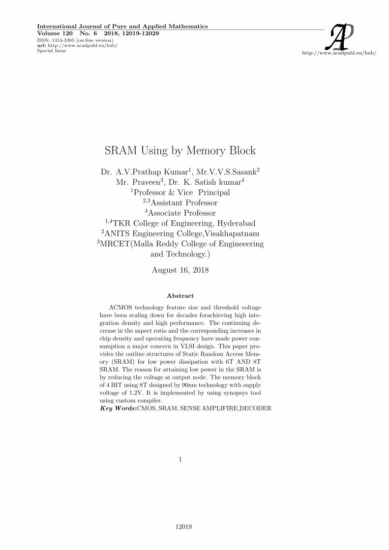
4. decoder
Fig 4: basic memory block
Decoder are used for enabling each memory cell which stores singlebit of data. Precharge is use to keep bit line and bit bar line to vddafter every operation.
3 DESIGN& IMPLEMENTATION OF
8T SRAM of 4 BITS MEMORY CIR-
CUIT
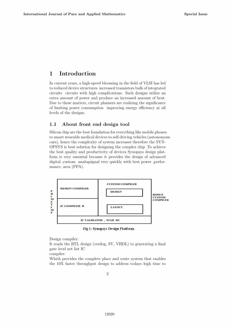
To implement 4 bit SRAM memory a 2-4 row decoder and 2-4column decoders is used. It is arranged in 4x4 matrixes (SRAM 8Tcell) form. Here the outputs of the row decoder are connected to theSRAM cells word line wl and the bit lines of all cells are connectedto the column decoder. When the input to the decoder is 00, theword line wl of first row become high and all the SRAM cell areconnected to the bit line. But depending upon the address of thecolumn decoder one column will be chosen. In this way a particularcell of the SRAM memory array will be picked. For example if00will be the address for both row decoder and column decoder,then a particular cell whose location is 00 in the memory array willbe selected. If address of the row decoder is 00 but the address ofthe column decoder is 01 then second SRAM cell of the first row isselected. Fig 6 shows the schematic of 4 bit sram cell. Simulationshave been performed using SPICE based on SAE(Simulation and
5
International Journal of Pure and Applied Mathematics Special Issue
12023
Analysis Environment) 0.9m CMOS technology with supply voltageof 1.2V.
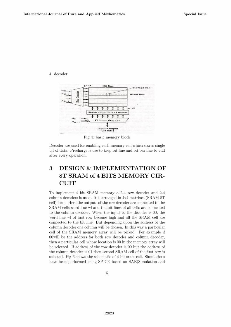
4 EXPERIMENTAL RESULT
Output wave forms of conventional and proposed 6T SRAM areshown in Fig 6 and Fig 7.
6
International Journal of Pure and Applied Mathematics Special Issue
12024
Tabulation of Simulation results:
5 CONCLUSION
Proposed work consists of SRAM memory design using SYNOP-SYS TOOL, observed that SRAM 8T cell dissipates less power incomparison to 6T transistor SRAM cell as the temperature rises.The SRAM 8T transistor SRAM cell dissipates less power at dif-ferent power supply voltages in comparison to SRAM 6T cells. Asthe supply voltage down the power dissipation also reduced. The8T transistor SRAM dissipates less power at higher bit-line capaci-tance in comparison to SRAM 6T transistor. Implemented the 4bitmemory unit.
References
[1] Martin Margala, Low-Power SRAM Circuit Design in IEEEConference: Memory Technology, Design
and Testing, 1999.
7
International Journal of Pure and Applied Mathematics Special Issue
12025
[2] Evelyn Grossar, Michele Stucchi, Karen Maex, and WimDe-haene, Read Stability and Write-Ability Analysis of SRAMCells for Nanometer Technologies in IEEE Journal of SolidState Circuits, Vol 41, No.11,
November 2006.
[3] S.kumar V, A. Noor, Characterization and Comparison of lowpower SRAM cells in Journal of Electron
Devices, Vol.11, 2011.
[4] P.Upadhyay, S.K.Chhotray, R. Kar, D,Mandal, S.P.GhosalAnalysis of Static Noise Margin and Power Dissipation of aProposed Low Voltage Swing 8T SRAM cell in IEEE Confer-ence on Information and
Communication technologies (ICT 2013).
[5] Kevin Zhang, Yih Wang Low-Power SRAMs in NanoscaleCMOS Technologies in IEEE Transactions
On ElectrOn Electron Devices, Vol. 55, No.1, January 2008.
[6] Dinesh Sangwan, DevenderRatheeA study on design and anal-ysis of SRAM & DRAM International
Journal of Enhanced Research in Science Technology & Engi-neering, Vol. 2 Issue 7, July-2013.
[7] Hiroyuki Yamauchi, A Discussion on SRAM Circuit DesignTrend in Deeper Nanometer-Scale
Technologies IEEE Transactions On Very Large Scale Integra-tion (VLSI) Systems, Vol.18.No.5, May 2010.
Authors details
8
International Journal of Pure and Applied Mathematics Special Issue
12026
Dr. A.V.Prathap Kumar is working as a professor in ECE andDean of academics in TKR Engineering college. He published manyNational and International journals and he received Best teacheraward. He conducted many workshop sand international confer-ences. Under his Guidance 6 Research Scholars doing in differentareas. He worked as a R&D Head in K.L.University. And also heworked as Principal in Various Colleges affiliated to JNTUA. Healso act as IEEE, conference judge. he is a life member of ISTE.
Mr.V.V.S.Sasank, received his B.tech and M.tech Degree from GI-TAM University, Visakhapatnam, Andhra Pradesh, India. He got1st rank in M.tech CST from GITAM University. Presently he isworking as Assistant Professor in the IT Department of ANITSEngineering College,Visakhapatnam since one year. He activelyparticipated in various workshops and seminars and presented pa-pers related to information technology. His areas of interests aredata mining, database management system and image processing.
9
International Journal of Pure and Applied Mathematics Special Issue
12027
Mr. Praveen working as Asst.professor in computer science Engi-neering in MRCET(Malla Reddy College of Engineeering and Tech-nology), Hyderabad,Telangana. He is having 2 years of teaching ex-perience and 1.5 year in Industry Experience as Hardware Engineerin HCL Infosystems. He received M.Tech Computer science Engi-neering from GITAM University. He is one of the active memberin Co-Curricular Activities. Presented many paper presentationsand participated in many events. His area of interest include datamining, data warehousing, database system.
10
International Journal of Pure and Applied Mathematics Special Issue


![Design and analysis of SRAM cell for ULP application... Timing Diagram of 8T SRAM cell 1.2.69T SRAM cell Figure.9. is the architecture of 9T SRAM cell[8]. It consists of 03 extra transistors](https://static.documents.pub/doc/80x56/5ace04837f8b9ad13e8ecb0a/design-and-analysis-of-sram-cell-for-ulp-application-timing-diagram-of-8t-sram.jpg)


![Analysis of 6T FinFET SRAM Assist Techniques and …djseo/classes/ee241/...EE241 Final Report 2 (a) (b) (c) Fig. 1 FinFET-based SRAM cell array published by [1]. High Density Cell](https://static.documents.pub/doc/80x56/5ae6f2697f8b9a6d4f8d666f/analysis-of-6t-finfet-sram-assist-techniques-and-djseoclassesee241ee241.jpg)

![IEEE TRANSACTIONS ON VERY LARGE SCALE INTEGRATION … · Schmitt-trigger-based cell [17], whose performance degrades at nominal voltages. Therefore, we have chosen a simple 8T SRAM](https://static.documents.pub/doc/80x56/5f1334a8fd00ec65d621269b/ieee-transactions-on-very-large-scale-integration-schmitt-trigger-based-cell-17.jpg)


