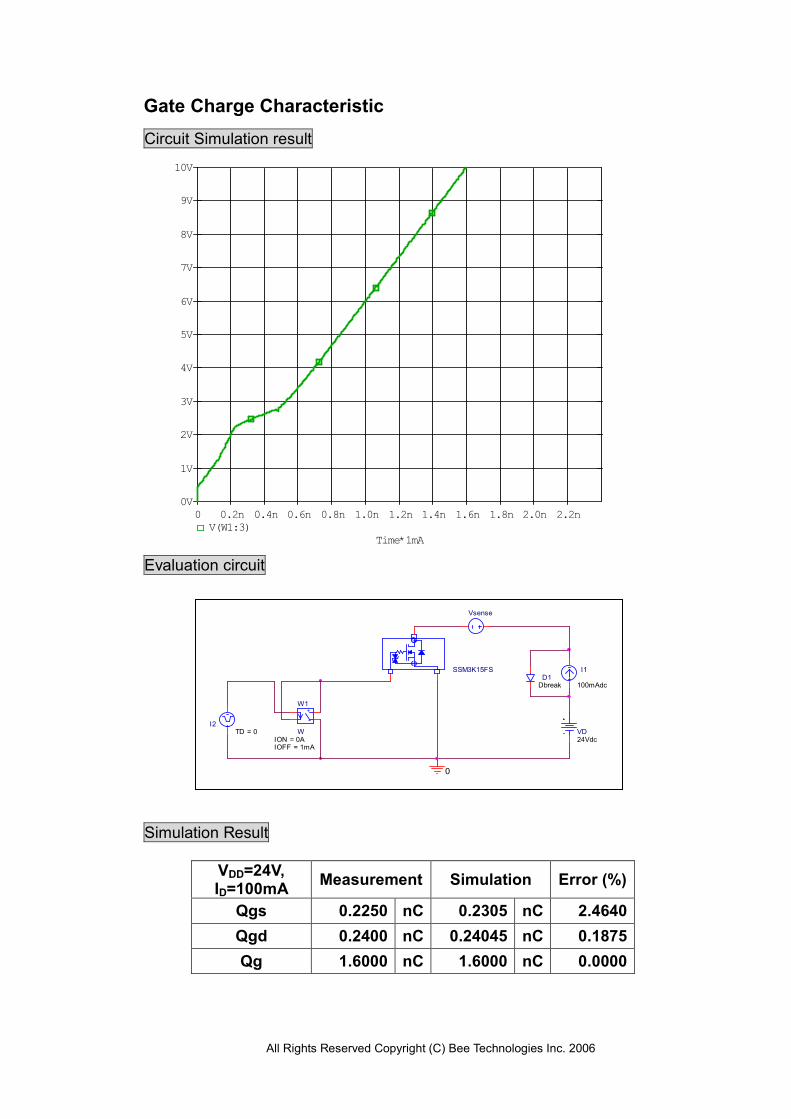
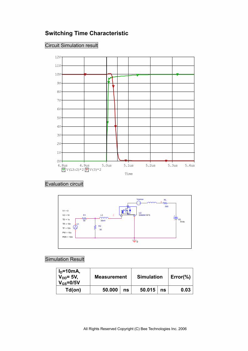
All Rights Reserved Copyright (C) Bee Technologies Inc. 2006
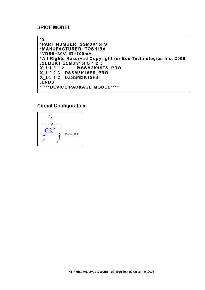
.SUBCKT MSSM3K15FS_PRO D G S CGD 1 G 1p R1 1 G 10MEG S1 1 D G D SMOD1 D1 2 D DGD R2 D 2 10MEG S2 2 G D G SMOD1 M1 D G S S MSSM3K15FS .MODEL SMOD1 VSWITCH( VON=0V VOFF=-10mV RON=1m ROFF=1E12) .MODEL DGD D ( CJO=7.8416E-12 M=.42015 VJ=90.500E-3 .MODEL MSSM3K15FS NMOS + LEVEL=3 L=720.00E-9 W=.2192 KP=732.66E-9 RS=10.000E-3 + RD=.3567 VTO=1.5453 RDS=1.0000E6 TOX=40.000E-9 + CGSO=7E-15 CGDO=45E-12 + CBD=1e-009 MJ=.39887 PB=.93267 RG=418 + NFS=1.0E+12 ETA=0.01 + IS=1E-15 N=5 RB=1 .ENDS *****MOSFET PROFESSIONAL MODEL*****
S
DGD
G
R2
10MEGR1
10M CGD
+
-
+
-
S1
S
D
Q1
+
-
+
-
S2
S
MOSFET SPICE MODE
Equivalent Circuit
All Rights Reserved Copyright (C) Bee Technologies Inc. 2006
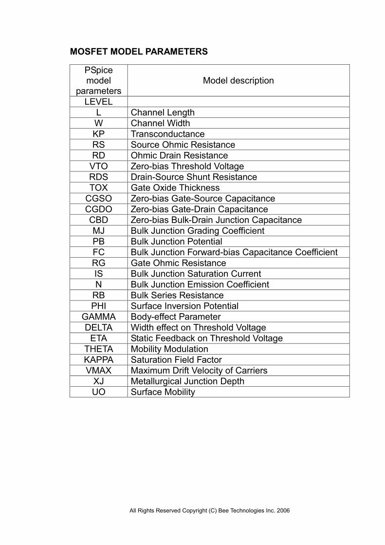
MOSFET MODEL PARAMETERS
PSpice model
parameters Model description
LEVEL
L Channel Length
W Channel Width
KP Transconductance
RS Source Ohmic Resistance
RD Ohmic Drain Resistance
VTO Zero-bias Threshold Voltage
RDS Drain-Source Shunt Resistance
TOX Gate Oxide Thickness
CGSO Zero-bias Gate-Source Capacitance
CGDO Zero-bias Gate-Drain Capacitance
CBD Zero-bias Bulk-Drain Junction Capacitance
MJ Bulk Junction Grading Coefficient
PB Bulk Junction Potential
FC Bulk Junction Forward-bias Capacitance Coefficient
RG Gate Ohmic Resistance
IS Bulk Junction Saturation Current
N Bulk Junction Emission Coefficient
RB Bulk Series Resistance
PHI Surface Inversion Potential
GAMMA Body-effect Parameter
DELTA Width effect on Threshold Voltage
ETA Static Feedback on Threshold Voltage
THETA Mobility Modulation
KAPPA Saturation Field Factor
VMAX Maximum Drift Velocity of Carriers
XJ Metallurgical Junction Depth
UO Surface Mobility
All Rights Reserved Copyright (C) Bee Technologies Inc. 2006
0
0.1
0.2
0.3
0.4
0 0.05 0.1 0.15 0.2
DRIAN CURRENT ID (A)
TRANSCO
NDUCTANCE G
fs(s
)
Measurement
S imulation
Transconductance Characteristic
Circuit Simulation Result
Comparison table
Gfs(S)
Id(A) Measurement Simulation
Error(%)
0.005 0.0476 0.0481 0.96
0.01 0.0667 0.0690 3.45
0.02 0.1000 0.0966 -3.38
0.05 0.1515 0.1524 0.61
0.1 0.2128 0.2155 1.29
0.2 0.3077 0.3044 -1.07
All Rights Reserved Copyright (C) Bee Technologies Inc. 2006
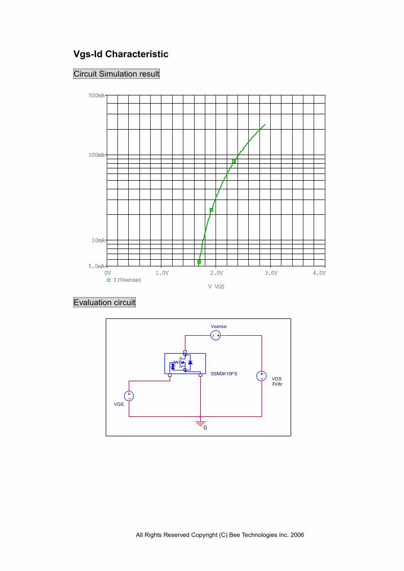
0
SSM3K15FS
VGS
Vsense
VDS3Vdc
Vgs-Id Characteristic
Circuit Simulation result
Evaluation circuit
V_VGS
0V 1.0V 2.0V 3.0V 4.0V
I(Vsense)
10mA
100mA
5.0mA
500mA
All Rights Reserved Copyright (C) Bee Technologies Inc. 2006
0.001
0.01
0.1
1
1 2 3
GATE-SOURCE VOLTAGE VGS (V)
DRAIN
CURRENT ID (A)
MeasurementSimulation
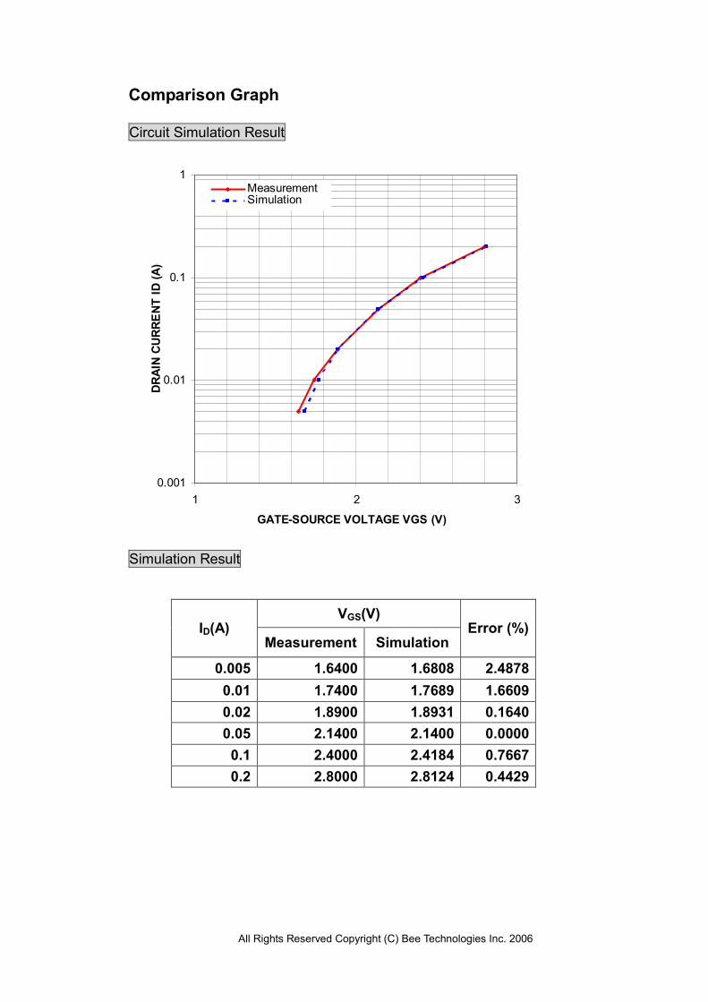
Comparison Graph Circuit Simulation Result
Simulation Result
VGS(V) ID(A)
Measurement Simulation Error (%)
0.005 1.6400 1.6808 2.4878
0.01 1.7400 1.7689 1.6609
0.02 1.8900 1.8931 0.1640
0.05 2.1400 2.1400 0.0000
0.1 2.4000 2.4184 0.7667
0.2 2.8000 2.8124 0.4429
All Rights Reserved Copyright (C) Bee Technologies Inc. 2006
0
Vsense
VDSSSM3K15FS
VGS4Vdc
V_VDS
0V 20mV 40mV 60mV 80mV 100mVI(Vsense)
0A
2mA
4mA
6mA
8mA
10mA
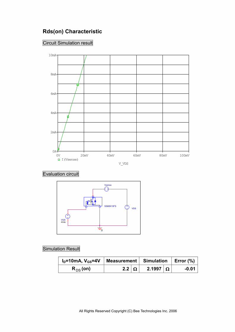
Rds(on) Characteristic
Circuit Simulation result
Evaluation circuit
Simulation Result
ID=10mA, VGS=4V Measurement Simulation Error (%)
RDS (on) 2.2 ΩΩΩΩ 2.1997 ΩΩΩΩ -0.01
All Rights Reserved Copyright (C) Bee Technologies Inc. 2006