Page 1
HAL Id: hal-01942286https://hal.archives-ouvertes.fr/hal-01942286
Submitted on 11 Dec 2018
HAL is a multi-disciplinary open accessarchive for the deposit and dissemination of sci-entific research documents, whether they are pub-lished or not. The documents may come fromteaching and research institutions in France orabroad, or from public or private research centers.
L’archive ouverte pluridisciplinaire HAL, estdestinée au dépôt et à la diffusion de documentsscientifiques de niveau recherche, publiés ou non,émanant des établissements d’enseignement et derecherche français ou étrangers, des laboratoirespublics ou privés.
Stress in thin films and coatings: Current status,challenges, and prospects
Grégory Abadias, Eric Chason, Eric Keckes, Marco Sebastiani, GregoryThompson, Etienne Barthel, Gary Doll, Conal Murray, Chris Stoessel, Ludvik
Martinu
To cite this version:Grégory Abadias, Eric Chason, Eric Keckes, Marco Sebastiani, Gregory Thompson, et al.. Stressin thin films and coatings: Current status, challenges, and prospects. Journal of Vacuum Scienceand Technology A, American Vacuum Society, 2018, 36 (2), pp.020801. �10.1116/1.5011790�. �hal-01942286�
Page 2
1
Stress in thin films and coatings: Current status, challenges and prospects
G. Abadias1*
, E. Chason2, J. Keckes
3, M. Sebastiani
4, G.B. Thompson
5
E. Barthel6, G.L. Doll
7, C.E. Murray
8, C.H. Stoessel
9, L. Martinu
10
1 Institut Pprime, Département de Physique et Mécanique des Matériaux, UPR 3346, CNRS-
Université de Poitiers-ENSMA, SP2MI, Téléport 2, F86962 Futuroscope-Chasseneuil, France
E-mail : [email protected]
2 School of Engineering, Brown University, Providence, Rhode Island 02912-9104, USA
E-mail: [email protected]
3 Department of Materials Physics, Montanuniversität Leoben and Erich Schmid Institute for
Materials Science, Austrian Academy of Sciences, Leoben, Austria
E-mail: [email protected]
4 University of Rome “ROMA TRE”, Engineering Department, Via della Vasca Navale 79,
Rome, Italy, E-Mail: [email protected]
5 Department of Metallurgical & Materials Engineering, The University of Alabama, PO Box
870202, Tuscaloosa, Alabama 35487-0202, USA
E-mail: [email protected]
6Laboratoire Sciences et Ingénierie de la Matière Molle, PSL Research University, ESPCI
Paris, CNRS, et Sorbonne Universités, UPMC Univ Paris 06, F-75231 Paris Cedex 05,
France, E-mail: [email protected]
7Mechanical Engineering Department, The University of Akron, Akron OH, 44325-0406
E-mail: [email protected]
8IBM T.J. Watson Research Center, Yorktown Heights, NY 10598
E-mail: [email protected]
9Eastman Chemical Co., 3788 Fabian Way, Palo Alto, CA94303, USA
E-mail: [email protected]
10
Department of Engineering Physics, Polytechnique Montréal, Montreal, QC, Canada,
E-mail: [email protected]
* Corresponding author
Page 3
2
Abstract
The issue of stress in thin films and functional coatings is a persistent problem in
materials science and technology that has congregated many efforts, both from experimental
and fundamental points of view, to get a better understanding on how to deal with, how to
tailor and how to manage stress in many areas of applications. With miniaturization of device
components, the quest for increasingly complex film architectures and multi-phase systems,
and the continuous demands for enhanced performance, there is a need towards the reliable
assessment of stress on a sub-micron scale from spatially-resolved techniques. Also, the stress
evolution during film and coating synthesis using physical vapor deposition (PVD), chemical
vapor deposition (CVD), plasma enhanced chemical vapor deposition (PECVD) and related
processes is the result of many interrelated factors and competing stress sources, so that the
task to provide a unified picture and a comprehensive model from the vast amount of stress
data remains very challenging.
This article summarizes the recent advances, challenges and prospects of both
fundamental and applied aspects of stress in thin films and engineering coatings and systems,
based on recent achievements presented during the 2016 Stress Workshop entitled “Stress
Evolution in Thin Films and Coatings: from Fundamental Understanding to Control”.
Evaluation methods, implying either wafer curvature, X-ray diffraction (XRD) or focused ion
beam (FIB) removal techniques, are reviewed. Selected examples of stress evolution in
elemental and alloyed systems, graded layers and multilayer-stacks, as well as amorphous
films deposited using a variety of PVD and PECVD techniques are highlighted. Based on
mechanisms uncovered from in situ and real-time diagnostics, a kinetic model is outlined that
is capable of reproducing the dependence of intrinsic (growth) stress on grain size, growth
rate and deposited energy. The problems and solutions related to stress in the context of
optical coatings, inorganic coatings on plastic substrates, and tribological coatings for
aerospace applications, are critically examined.
This review also suggests strategies to mitigate excessive stress levels from novel coating
synthesis perspectives to microstructural design approaches, including the ability to empower
crack-based fabrication processes, pathways leading to stress relaxation and compensation, as
well as management of the film and coating growth conditions with respect to energetic ion
bombardment. Future opportunities and challenges for stress engineering and stress modelling
are considered and outlined.
Page 4
3
Table of content
I. Introduction
II. Evaluation methods for stress determination
A. A nondestructive method: wafer curvature
B. X-ray Diffraction techniques
C. FIB-based methods
D. Methods validation and critical comparison among available measurement
techniques
III. Stress in polycrystalline films: Current models and selected examples
A. Modeling stress development during polycrystalline thin film growth
B. The impact of interface reactivity, alloying and phase transformation on stress
C. Stress gradient and texture development
IV. Stress in engineering coatings and coating systems
A. Stress in microfabricated systems
B. Stress in optical coatings
C. Stress in the coatings on plastics
D. Effects of stress on the performance of tribological coatings for aerospace
applications
E. Key aspects and complementary strategies to tailor intrinsic stress
F. Living with cracks
V. Conclusions and outlooks
Page 5
4
I. Introduction
The presence of stress in thin films and functional coatings constitutes a major concern in
many technological applications as excessive residual stress levels can dramatically affect the
performance, reliability and durability of material components and devices. Worst case
scenarios lead to film cracking for layers subjected to tensile stress1,2
or peeling off, buckling
or blistering in the case of compressive stress.3–6
Residual stress distributions can significantly
impact the adhesion and the fracture toughness of thin films,7–9
the ductility of bulk metallic
glasses (BMG),10
the performance of optoelectronic and aerospace components,11
the thermo-
mechanical behavior of stacks in Through Silicon Vias (TSV) 3D integrated devices,12
the
resonant frequency and lifetime of micro- and nano-electro-mechanical systems (MEMS and
NEMS),13
or cause the emergence of hillocks and whiskers in metal interconnects at the origin
of short circuit failures,14–17
to cite a few examples. Alternately, stress (or strain) can have
beneficial influence on the physical properties of thin layers and nanostructures, e.g.
conductivity,18
dielectric permittivity,19
piezoelectricity, magnetic anisotropy and magneto-
elastic coupling,20,21
or enhancement in charge carrier mobility in silicon-based semiconductor
technology.22
Therefore, there is significant motivation to understand the origin of stress in
thin films as they can directly affect the design, processing and lifetime of advanced materials
and components. Various research strategies to tailor and control the stress state are currently
devised in diverse applications ranging from micro/optoelectronic devices, MEMS/NEMS
(thermal sensors and actuators), optical components (lenses, mirrors, filters, etc..) to
protective and functional coatings intended to impart thermal, mechanical, tribological,
environmental, electrical, magnetic or biological functions. From a technological point of
view, this has generated an intense research and innovation activity over the last decades
related to the measurement of residual stresses, more recently including the determination of
Page 6
5
intrinsic (growth) stress due to thin film deposition conditions, which has gained interest
thanks to the potential offered by in situ and real-time diagnostics.23
Regardless of the technique of film preparation (physical or chemical vapor deposition
(PVD/CVD), electrochemical deposition, etc) thin films can develop large intrinsic stresses in
the course of their growth process. For many materials, the stress magnitude in thin layer
forms and nanostructures can typically exceed the tensile strength of their respective bulk
counterpart.24,25
Indeed, the density of defects that are frozen into a film during deposition can
be two orders of magnitude higher than that produced by the severest cold-work treatment of
a bulk material.26
The concern about stress dates back over a century ago with the observation by Gore that
“the inner and outer surfaces of electrodeposits were in unequal states of cohesive tension”,
causing the plate on which they were deposited to bend.27
This led Stoney28
, some years later,
to derive a relationship between the film stress and the amount of substrate bending, which
can be readily quantified from the measurement of the substrate curvature, or equivalently, its
deflection. Since the pioneer work of Stoney in the early 1900s, considerable work has been
done, especially after 1960s with the achievement of high vacuum conditions during the PVD
processes,29–32
enabling one to separate the various parameters of film growth that influence
the intrinsic film stress while minimizing the influence of impurity content due to chemical
reactivity with residual gas components. Despite that many trends have been identified, in
particular the common stress behaviors depending on material mobility,33–37
the stress
development during thin film growth exhibits complex dependences with respect to the
growth rate, temperature, film microstructure and morphology, so that a complete and
unifying picture of our understanding of stress has not yet been achieved. The situation gets
even more intricate in the case of multicomponent systems, where alloying effects such as
solute atom segregation38,39
or phase transformation40,41
may come into play. Deposition
Page 7
6
processes in which the temporal and energetic profiles in terms of energy and fluxes of
specific species (such as ions) can be manipulated42–45
are opening new avenues for stress
tailoring. This explains why stress is a hot topic amongst the materials science and
engineering community, calling for more systematic testing grounds as well as new
achievements gained from multiscale stress modeling.
From a more practical point of view, the reliable assessment of residual stresses on a
micron, or sub-micron, scale is a strategic challenge for the robust design and reliability of a
wide range of micro- and nano-systems. Protective thin films and coatings often possess
complex gradients of phases, microstructure and residual stresses, which result from (i)
intentionally varying deposition conditions, (ii) self-organization phenomena like competitive
grain growth, diffusion along GBs and/or on the surface, (iii) post-deposition mechanical and
thermal loads caused, for example, by friction between coating and machined surface, and (iv)
the effect of the surrounding environment leading to gas or vapor sorption. Those gradients
decisively influence the functional properties of thin films and coatings, such as hardness,
toughness, oxidation resistance, wear behavior, adhesion and durability. Therefore, in order to
optimize the functional properties, it is necessary to assess the depth variation of residual
stresses with respect to the microstructure with nanoscale resolution. The evolution of the
average in-plane stress can be measured by wafer curvature techniques during deposition,
providing information on the stress profile throughout the film thickness.23 In recent years,
several high-resolution residual stress measurement techniques have been implemented, such
as micro-focus synchrotron X-ray diffraction (XRD),46
holographic transmission electron
microscopy (TEM),47
micro-Raman spectroscopy,48
and electron backscattered diffraction
(EBSD)49
. Unfortunately, most of these methods have limitations in terms of instrument
accessibility, applicability to amorphous (or strongly textured) materials, perfect lattice
rectification and to non-homogeneous stress states. Nonetheless, the measurement of residual
Page 8
7
stress in sub-micron volumes is still a challenging task, especially in the case of strongly
textured, complex multiphase, nano-crystalline or amorphous materials and films.
This article, which gathers contributions from several leading groups working in the field,
encompasses a critical viewpoint on to-date state of knowledge on stress in thin films and
coatings. It gives a non-exhaustive overview and a snapshot on the progress of both
fundamental and applied research deployed in this field, based on recent outcomes presented
during the Stress Workshop entitled “Stress Evolution in Thin Films and Coatings: from
Fundamental Understanding to Control”, that was jointly organized by the Advanced Surface
Engineering Division (ASED) of the American Vacuum Society (AVS) and the Society of
Vacuum Coaters (SVC), in Chicago, in October 2016. It is mostly focused on polycrystalline
thin films, so that the issue of strained surfaces and nanostructures, as well as epitaxial layers,
will not be discussed here. The reader interested in such aspects is referred to the
articles/monographs of Koch50, Ibach51, Brovko et al.52 and Fluri et al.53
Similarly, for more
extensive reviews of this work, particularly on the proposed stress models, it is advisable to
go through the recent tutorial of Chason and Guduru.23
Still, stress in amorphous thin films
represents an important part of technological interests especially in relation to optical coatings
and thin films on plastics.11,54–56
The present paper is divided into several parts. Sections II and III are dedicated to the
fundamental aspects of how thin film stress can be measured and interpreted. In Section II, we
outline the evaluation methods for stress determination, including wafer curvature, XRD and
focused ion beam (FIB)-based techniques. Section III describes recent experimental findings
on stress evolution during thin film growth and their understanding based on a kinetic model,
recently extended to account for energetic particle bombardment during deposition (Sec. III-
A). Selected examples are also provided to highlight chemical alloying effects and phase
transformation (Sec. III-B), as well as the interplay between stress gradient and texture
Page 9
8
development (Sec. III-C). Section IV addresses the ways how to deal with, how to tailor and
manage stress in specific areas of applications. These include the methods and approaches to
assess and control stress in microfabricated systems such as microelectronic components
(Section IV-A), or issues related to the effect of deposition processes and film growth
conditions in the context of most frequent amorphous and polycrystalline optical coatings
(OC) and optical interference filters (OIF), as well as strategies to mitigate excessive stress by
both experimental and design approaches (Section IV-B). Section IV-C gives an overview of
problems and solutions related to stress in the context of inorganic coatings on plastic
substrates, including polymer webs and injection molded components, while Section IV-D
describes case studies related to stress build up and stress compensation approaches in the
context of protective coatings for aeronautical, aerospace and related manufacturing
components. Complementary stress engineering strategies, based on interfacial and alloying
design or pulse management in sputtering processes, are proposed in Section IV-E, followed
by an overview of the present status of understanding and interpreting the formation of cracks
and their propagation in relation to stress (Section IV-F). Finally, Section V summarizes the
still open question related to stress, and it suggests pathways and outlooks for future
developments.
II. Evaluation methods for stress determination
A. A nondestructive method: wafer curvature
An important method for measuring stress in thin films is wafer curvature. The principle behind
the method is to measure the curvature induced in the substrate due to stress in the film. Because it
is non-destructive and can be used in real-time, it has been one of the workhouse techniques for
quantifying stress in thin films.23,33,57,58
In this section, we describe how the curvature is related to
the film stress and make clear some underlying assumptions used in interpreting the measurements.
Page 10
9
We will also discuss some methods that have been developed for measuring stress using wafer
curvature.
The well-known Stoney equation relates the average stress in the film ( ) to the measured
curvature (κ)59
:
(1).
The values Ms and hs refer to the biaxial modulus and thickness of the substrate, respectively.
The product fh is termed the stress-thickness and has units of force/length; note that the average
stress cannot be determined from the curvature without knowing the film thickness. The average
stress in the Stoney equation is assumed to be equi-biaxial and laterally uniform. This ignores, for
instance, that in polycrystalline films the stress may be different at/near the grain boundaries (GBs)
than in the middle of the grain23,60
or that in patterned films (such as metallic interconnect lines) the
stress may be non-uniform over the surface61
.
Even assuming that the stress is laterally uniform, it may still vary through the thickness of the
film. Then the thickness-averaged stress can be computed by integrating the in-plane stress at height
z from the substrate (σxx(z)) over the film thickness (hf):
(2).
In this discussion, we are ignoring the presence of any surface or interfacial stresses that may
also contribute to the curvature.62–64
Because of the thickness averaging, a single curvature
measurement does not provide any information about the depth-dependence of the stress in the film.
The curvature from a film with a non-uniform stress through the thickness is equivalent to a film of
the same thickness with a uniform stress of the average value. A film that induces no curvature in
the substrate may in fact have a large stress gradient in it. The lack of curvature only tells us that the
tensile and compressive stresses integrated over the thickness are equal. Since large stress gradients
2
6
ss
f
hM
h
fh
xx
f
dzzh
0
)(1
Page 11
10
may lead to cracking even though the nominal stress appears to be small, it is important to know the
distribution of stress throughout the film’s thickness.
The depth-dependence of the stress can be explored by measuring the evolution of the stress-
thickness as the film is deposited. The time derivative of the stress-thickness is given by:
(3),
where h is the thickness at time t. The first term on the right corresponds to the effect of adding new
layers to the surface with a stress of σxx(h); this is sometimes referred to as the incremental or
instantaneous stress. The second term corresponds to a change in the stress of the layers that have
already been deposited.
If we can assume that the stress does not change after deposition (i.e., the time derivative in the
second term in Eq. (3) is zero), then the stress at each height in the film is the same as when it was
deposited. In that case, the incremental stress can be determined from the derivative of the stress-
thickness with thickness:
dh
hd
dt
dh
dt
hd
hxx
)()(
)(
(4).
To illustrate how this works, a schematic representation of a film of thickness hf with a
distribution of in-plane stress is given in Figure 1a. The arrows represent the stress at different
heights in the film. The arrows pointing away from the film correspond to tensile stress and those
pointing toward the film correspond to compressive stress. The corresponding evolution of the
curvature during deposition is shown in Figure 1b as a function of thickness with the value hf shown
by the vertical dotted line. The average film stress at this thickness is determined by dividing the
measured curvature by the thickness, represented by the line between the measured value and the
h
xxxx dz
t
z
dt
dhh
dt
hd
0
)()(
)(
Page 12
11
origin. The incremental stress at this thickness is represented by the slope of the stress-thickness at
this point, represented by the tangent line on the curve. Note that at this thickness the average stress
is positive (tensile) while the incremental stress is negative (compressive). The data are taken from
stress-thickness measurements during electron beam evaporation of polycrystalline Ag on SiO2.65
Figure 1: a) Schematic showing the distribution of stress throughout the thickness of a film on a
substrate. b) Evolution of stress-thickness during electron-beam deposition of Ag on SiO2. The
slope of the line from the origin to the solid circle at hf is proportional to the average stress. The
slope of the tangent line is proportional to the incremental stress. c) Evolution of the stress-
thickness when the deposition is terminated.
Recall that in equating the incremental stress with the slope of the stress-thickness, we assumed
that the stress in the deposited layers does not change. The effect of the stress changing in the
deposited layers can be seen when the growth is stopped at a thickness of 100 nm indicated by the
vertical line (Figure 1c). Since there is no more growth, the thickness of the film does not change
after this point. However, it is clear that the stress-thickness relaxes significantly. As discussed
below, this may be due to various stress-induced processes like diffusion of atoms out of the grain
boundary (GB), thermal expansion mismatch or grain growth in the film.
Multiple techniques have been developed for measuring the wafer curvature. Some methods
monitor the change in shape of the cantilever by capacitance66–68
, microbalance,69
dilatometry or
interferometry.70
Others monitor the deflection of light beams reflected from the cantilever surface.
Page 13
12
Some monitor a single reflected beam71
or the spacing between multiple beams reflected from the
surface.23,72,73
A benefit of the multi-beam reflection method is that it reduces the sensitivity to
sample vibration because the curvature is determined from the change in spacing between the
reflected beams. Vibration of the sample may change the direction of the reflected beams, but it
changes them all by the same amount so that the relative spacing between the beams does not
change. Multiple-beam optical stress sensor (MOSS) is therefore useful for in situ measurements in
growth chambers where vacuum pumps may induce a large amount of mechanical vibration, as well
as in liquid media, such as during electrochemical deposition,74,75
where convection (natural or
forced) may induce perturbations.
B. X-ray diffraction techniques
1. Conventional laboratory XRD
Conventional laboratory XRD analysis performed in reflection geometry is routinely used
to characterize average residual stresses and stress gradients in thin films, coatings and near-
surface regions.76–80
Residual stress is determined from the measurement of X-ray elastic
strains, and applying a constitutive equation in the form of a generalized Hooke’s law,
which requires the knowledge of the elastic properties of the film.79
The common procedure
employs the so-called ‘sin2 method’, based on the determination of a set of lattice spacings
hkld using Bragg’s law from the measured Bragg’s angle positions hkl
of hkl reflections at
various sample tilt angles and azimuth angles , whereby represents the angle between
the diffraction vector Q and the sample normal z, and is the rotation angle around z. In many
situations, polycrystalline films exhibit a preferred crystallite orientation of rotational
symmetry around the substrate normal, referred to as a fiber texture, so that it is sufficient to
measure the strain solely as a function of the tilt angle . In the absence of shear stress
components (ij=0 for ij), and assuming an equi-biaxial in-plane stress state (11=22= ),
Page 14
13
the quantity can be readily extracted from the slope of hkld versus sin2 curve, according
to the fundamental equation of x-ray residual stress analysis
(5)
where and
refer to the x-ray elastic constants (XECs), and d0 is the unstrained
lattice parameter. XEC quantities are introduced in the formalism to account for the elastic
anisotropy of crystalline materials. For randomly textured materials, they are independent
of (and ) and can be calculated for each hkl reflection from the single crystal elastic
compliances sij using a grain interaction model.77,79,81
Indeed, in a diffraction experiment, only
a given subset of crystallites contribute to the measured intensity, so that a micromechanical
model relating the strain (or stress) inside these crystallites to the macroscopic average stress
to which the whole specimen is subjected, is required. The most common approximations are
the Reuss (all crystallites are subjected to the same stress),82
Voigt (all crystallites exhibit the
same strain),83
and Neerfeld-Hill limits,84,85
the last being the arithmetic mean of the Reuss
and Voigt estimates.77
Note that for isotropic materials, the XECs reduce to the mechanical
elastic constants, and
, defined as
and
, where E and
are the Young’s modulus and Poisson ratio of the deposit, respectively.
The value of the unstrained lattice parameter d0 can be obtained from the strain-free
direction , derived by stating from the fundamental Eq. (5), which yields
for the case of isotropic materials under an equi-biaxial stress state. In practice, when
the elastic constants of the deposit material are unknown (which is rather often the case for
multicomponent alloys or complex compounds), the strain-free lattice parameter may be
obtained from the intersection point of dhkl vs. sin2 lines obtained for the same deposit under
different stress states.86,87
Page 15
14
However, it is important to note that the lattice spacing hkld represents an average
quantity, which depends on the actual stress depth gradient, z , X-ray penetration depth, ,
chemical gradients influencing zd hkl
o and XRD experiment geometry. In practice, different
approaches can be implemented depending on the laboratory diffraction equipment. On a two-
circle diffractometer, a simple procedure consists in measuring a series of 2 scans around a
single hkl reflection at varying incident beam angles . In this asymmetric geometry, known
as the mode79,88
, the angle is given by . A second option is to use a glancing
angle scan (at fixed ) and determine the hkld lattice spacing of various hkl reflections which
correspond to different values. This approach is well suited for thick polycrystalline
coatings with random orientation of the crystallites, allowing for the selection of hkl
reflections at high 2 values with appreciable intensity, contributing to a higher accuracy in
the measurement of hkld values (misalignment issues of the diffractometer are minimized at
high scattering angle). However, for thin films, Bragg reflections at high scattering angles are
most often hardly measurable.79
A third option, for researchers having a four-circle
diffractometer, is to measure a series of symmetric scans at various inclination angles
of the sample holder around the diffractometer axis (known as mode79,88
, or side-inclination
method76
), allowing for a change in the angle independently of the detector rotation. This
geometry is the same as the one used for pole figure measurements, and has one great virtue
that the accessible tilt angle range is much larger than in the mode (for which ),
starting from =0° to almost =90°. Moreover, the penetration depth remains nearly constant
for a wide range of tilt angles (up to 30-40°).
One should keep in mind, however, that the analysis outlined above is only valid for
polycrystalline thin films/coatings having a random orientation of grains. Thin films/coatings
produced by PVD/CVD techniques rarely belong to this category, as they most often exhibit a
Page 16
15
crystallographic texture related to their specific columnar growth morphology, so that they
can no longer be treated as macroscopically elastically isotropic specimens. In this case, the
stress analysis is more complex, and one has to use the concept of x-ray stress factors to relate
stress and strain.79
Also, the available directions which yield sufficient diffracted intensity
are often restricted to small angular ranges near the intensity poles. However, rather simple
expressions can still be derived for the most common fiber textures, <100>, <110>, <111>
and <112>, when considering crystals with cubic symmetry.79,89
The plots of the strain in
the distinct poles versus sin2 do not generally fall on a straight line, even for a biaxial stress
state. The only exceptions are reflections of the type h00 and hhh, as well as the <111>
texture.
Another approach is offered for the case of thin films with strong and sharp texture (as
also found in epitaxial layers or cold-rolled materials), known as the crystallite group
method.88,90
This method was introduced in 1982 by Willemse et al.,91
and then adapted by
Baron and Hauk to fiber-textured coatings.92
It is based on considering the highly textured
film with a crystallographic growth texture along a given <uvw> direction as a single crystal
aligned along this corresponding ideal orientation, and measuring the lattice spacings of
various hkl planes in the same set of grains belonging to this <uvw> ideal orientation
(crystallite group), at specific angles corresponding to the intensity poles. General
expressions of the elastic strain vs. sin
2 have been reported by Clemens and Bain
90 for
materials with cubic symmetry and for equal or non-equal biaxial stress states. This
methodology is a special case of the sin2 technique discussed above; it differs by the fact
that the texture in the film is explicitly taken into account rather than using XECs or stress
factors to describe geometrical distributions of crystallites in the polycrystalline aggregate.
Kim et al.93
have employed a similar procedure to determine the biaxial stress state in sputter-
deposited AlCu films with a (111) preferred orientation.
Page 17
16
In addition to anisotropy issues in textured thin films, another possible cause for
deviation from linearity of hkld vs. sin2 plots is the presence of stress gradients along the
film thickness, especially when the film thickness is on the same order as the penetration
depth at =0°.89
Different concepts and methods have been proposed to determine the
residual stress gradient z along the surface normal z in equibiaxially stressed
polycrystalline thin films and coatings.79,89,94,95
Neglecting the chemical gradients, the
measured X-ray elastic strain can be expressed as:
0
0
d/exp
d/exp1
zz
zzzd
dd
dd
hkl
hkl
o
hkl
o
hkl
o
hkl
hkl (6),
where is the thin film depth and zd hkl
is the depth-dependent measured lattice spacing. By
varying the experiment geometry, e.g., by changing the angle , it is possible to determine X-
ray elastic strains hkl for various X-ray penetration depths . This information is then used
to calculate the unknown residual stress depth profile z , defined in the real space as a
function of z, by fitting its supposed usually polynomial dependence to the experimental
hkl dependence (Eq. (6)), expressed in the so-called Laplace space, by applying X-ray
elastic constants.94 Since there are, however, infinitely many z dependencies, which can
be fitted to the measured hkl dependence, the inverse Laplace space approach can be used
to evaluate residual stress gradients z only in simplified cases like shot-peened samples
with linear and/or monotonic z dependencies. An illustration will be given in Sect. IV.A
for stress gradients in capped layers. In many other cases, z dependencies can be very
complex, like stepwise or oscillatory, and can be even combined with the presence of
chemical gradients in the sample, smearing the measured hkld values. Therefore, there is a
Page 18
17
need to develop novel characterization approaches, which can be used to assess nanoscale
z dependencies in graded thin films and coatings.
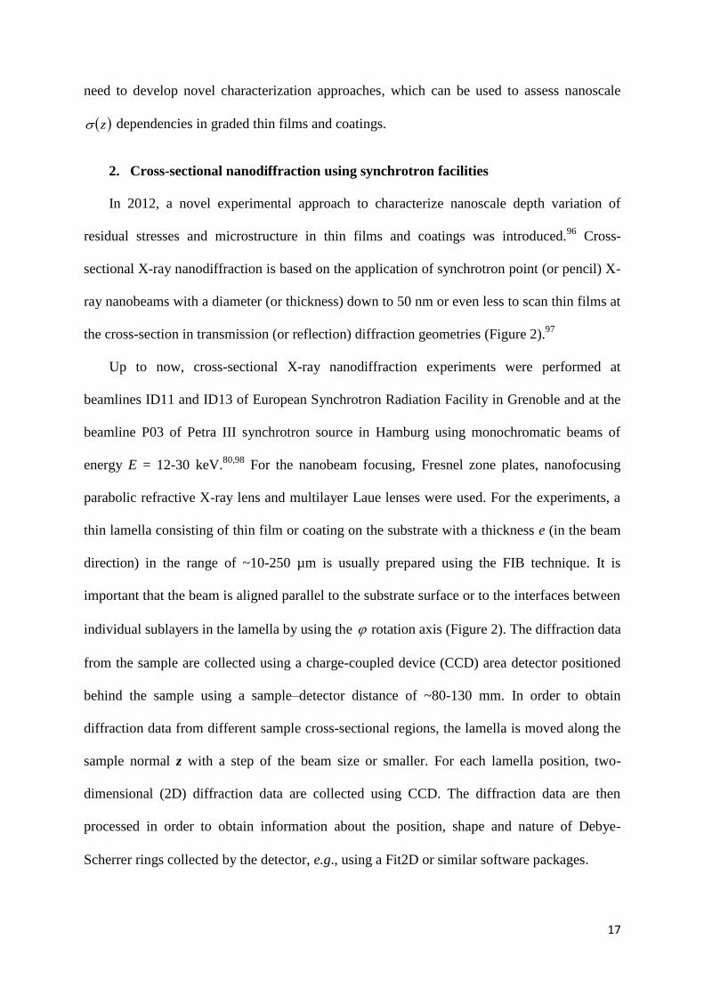
2. Cross-sectional nanodiffraction using synchrotron facilities
In 2012, a novel experimental approach to characterize nanoscale depth variation of
residual stresses and microstructure in thin films and coatings was introduced.96
Cross-
sectional X-ray nanodiffraction is based on the application of synchrotron point (or pencil) X-
ray nanobeams with a diameter (or thickness) down to 50 nm or even less to scan thin films at
the cross-section in transmission (or reflection) diffraction geometries (Figure 2).97
Up to now, cross-sectional X-ray nanodiffraction experiments were performed at
beamlines ID11 and ID13 of European Synchrotron Radiation Facility in Grenoble and at the
beamline P03 of Petra III synchrotron source in Hamburg using monochromatic beams of
energy E = 12-30 keV.80,98
For the nanobeam focusing, Fresnel zone plates, nanofocusing
parabolic refractive X-ray lens and multilayer Laue lenses were used. For the experiments, a
thin lamella consisting of thin film or coating on the substrate with a thickness e (in the beam
direction) in the range of ~10-250 µm is usually prepared using the FIB technique. It is
important that the beam is aligned parallel to the substrate surface or to the interfaces between
individual sublayers in the lamella by using the rotation axis (Figure 2). The diffraction data
from the sample are collected using a charge-coupled device (CCD) area detector positioned
behind the sample using a sample–detector distance of ~80-130 mm. In order to obtain
diffraction data from different sample cross-sectional regions, the lamella is moved along the
sample normal z with a step of the beam size or smaller. For each lamella position, two-
dimensional (2D) diffraction data are collected using CCD. The diffraction data are then
processed in order to obtain information about the position, shape and nature of Debye-
Scherrer rings collected by the detector, e.g., using a Fit2D or similar software packages.
Page 19
18
Figure 2: A schematic view of position-resolved X-ray nanodiffraction experiment carried out in
transmission diffraction geometry on CrN coating with a thickness deposited on Si(100)
substrate prepared as lamella with a thickness e. The sample is moved along the z axis with a
step of the X-ray beam size, and the diffraction data are collected using a CCD detector. The
beam is aligned parallel to the interface using the axis movement. A CrN hkl Debye–Scherrer
ring represents diffraction from CrN crystallites for which the diffraction vectors hkl
Q are
located on a bold line representing schematically Debye-Scherrer (D-S) ring depicted in the
stereographic projection in the top left. The orientation of the diffraction vector can be specified
by angles and . Reprinted with permission from Scripta Mater. 67, 748 (2012). Copyright
2012 Elsevier.
Every hkl Debye-Scherrer ring azimuthal position represents diffraction on (hkl)
crystallographic planes oriented with their normal vector nhkl parallel to the diffraction vector
zhkl
Q (Figure 2). Therefore, Debye-Scherrer rings collected using the 2D detector at the
thin film depth z can be used to evaluate the lattice spacing zd hkl
as a function of the ring
azimuthal angleusing Bragg’s law by analyzing Bragg’s angle zhkl
2 azimuthal
dependencies on the detector. Depending on the diffraction statistics, usually 36 values of
zd hkl
can be determined for 36 azimuthal angle sections called azimuthal cakes. Every
zd hkl
value represents an X-ray probe volume-averaged lattice parameter for the diffraction
Page 20
19
vector zhkl
Q orientation defined by the angles and in Figure 2. For every zd hkl
, X-ray
elastic strain at the thin film depth z can be determined as follows:
hkl
o
hkl
o
hklhkl
d
dzdz
(7).
The measured strain zhkl
can be expressed as a function of unknown strain components
zhkl
ij defined in the sample coordinate system with axes x, y and z from Figure 2 as follows:
zzz
zzzz
hklhklhkl
hklhklhklhkl
1232
2
31
33
22
22
22
11
2
sin2sin2sincoscos2sin
coscossincossin
(8).
By considering thin film X-ray elastic constants zS hkl
221 and zS hkl
1, which depend
on single crystal elastic constants, crystallographic texture, hkl reflection and grain interaction
mechanism, it is possible to write X-ray diffraction Hooke’s law as:
zzzzS
zzzzS
zzzzSz
hkl
hkl
hklhkl
1232
2
31221
33
22
22
22
11
2
221
3322111
sin2sincos2sincos2sin
coscossincossin
(9),
where zij represents unknown stress components defined in the sample coordinate system.
Usually, the stress state in thin films is equi-biaxial with zzz 2211, and the out-
of-plane stress component as well as shear stress components can be neglected with
033 z and 0zij . Consequently, Eq. (9) can be simplified:
222
221
1 sincossin2 zSzzSzz hklhklhkl (10).
Since for small Bragg’s angles the term 2sin and 2cos in Eq. (10) goes to zero and one,
respectively, Eqs. (6) and (10) can be rewritten as:
Page 21
20
zdzSz
zd hkl
o
hklhkl
22
1
2sin
(11).
It means that for every hkl Debye-Scherer ring and the corresponding zd hkl
dependence, the
in-plane residual stress is proportional to the Debye-Scherer ring ellipticity quantitatively
expressed through
2sin/ zd hkl.
In practical cases, zd hkl
values are evaluated for 36 azimuthal positionsof the hkl
Debye-Scherer rings, which are then plotted as a function of 2sin . The slope of the zd hkl
versus 2sin dependence is proportional to the magnitude of the in-plane stress z (Eq.
(11)). An important advantage of this approach is that the unstressed lattice parameter zd hkl
o
has to be determined only approximately.
In the case of thin lamella with the lamella thickness e comparable to or even smaller
than thin film or coating thickness (Figure 2), the lamella preparation results in the
relaxation of the stress component z11 , which influences the measured zhkl
as well as
the evaluated stress z . In that case, it is necessary to perform a finite element (FE)
modeling of the stress state in the thin lamellae in order to recalculate the stress state in the
unstressed sample as extensively discussed elsewhere.97
In majority of cases, it is possible to
prepare a lamellae with e , and the FE analysis is not required.
Another advantage of cross-sectional X-ray nanodiffraction is the fact that besides the
possibility to evaluate residual stress gradients, also thin film and coating depth gradients of
phases and microstructure (including texture and crystallite size) can be determined directly in
real space as a function of the coating depth z. This can be done by evaluating and comparing
individual Debye-Scherrer rings collected at different depths (Figure 2). The approach opens
Page 22
21
the possibility to analyze residual stress gradients in graded thin films with chemical gradients
and correlate them with depth gradients of texture, crystallite sizes and phases.
C. FIB-based methods
1. Method description and validation
In recent years, the development of FIB scanning electron microscopy (SEM) and Digital
Image Correlation (DIC) created new possibilities for the downscaling to the sub-micron scale
of material removal residual stress measurement techniques (e.g., hole drilling, ring-core and
slitting methods).99
The novel FIB techniques involve a combination of FIB milling, SEM imaging, DIC
analysis, and FE modelling.100–116
The method consists of incremental FIB milling, by using
several possible milling geometries, combined with in situ high-resolution field emission gun
SEM imaging of the relaxing surface, and a full field strain analysis by DIC. The through-
thickness profile of the residual stress can also be obtained by comparing the experimentally
measured surface strain with FE and/or analytical constitutive modeling.
FIB-DIC procedures have recently been established as the one method capable of
achieving sub-micron spatial resolution for the residual stress analysis in amorphous
materials, coatings and thin nanostructured layers.100–116
Kang and co-workers100
first
proposed the downscaling of the slitting method measuring the stress release caused by
milling of a slot on a thin diamond-like-carbon (DLC) film deposited on a glass substrate.
Several other milling relaxation geometries have been proposed in the literature, including
hole-drilling,101
ring-core,102–105
H-bar (also called double slot)110
, and four-slot geometries.112
The ring-core geometry has recently received particular attention because of its main
advantages of highest spatial resolution (< 1 µm), the possibility of full 2D strain and stress
mapping, and the fact that complete stress relaxation is achieved if the trench depth h is higher
Page 23
22
than the central stub’s diameter (dm), thus allowing for direct use of the Hooke’s law to
calculate the average residual stress from the measured strain relief. Additionally, the use of a
ring (or pillar) milling geometry could even be used to measure the fracture toughness of the
film, by using the nanoindentation pillar splitting method, which involves sharp
nanoindentation over the pillar to induce fracture of the material at a certain critical load that
can be correlated to the fracture toughness, by knowing the pillar’s radius. Since this section
is focused on the use of the ring-core geometry to measure residual stress, we refer to
previous papers for more details of the possible use of the same geometry to measure fracture
toughness.117,118
In Figure 3, a schematic representing the main steps of the method and examples of the
possible typical dimensions of the core are reported. More details on SEM imaging strategies
and DIC procedures are reported elsewhere.113
Figure 3: Schematic representation of the FIB-DIC method (ring-core) for residual stress
assessment at the micro scale. (a) SEM image acquired before FIB milling and definition of a
grid of markers, (b) FIB incremental milling and acquisition of one (or more) SEM images after
each milling step, (c) DIC to map relaxation strain and (d) extraction of the relaxation strain as a
function of milling depth. In (e-f), the typical size of the milled trench can vary between 1 and
20 µm.
Page 24
23
Significant activities in terms of validation of the method have recently been performed,
including comparisons with other standard measurement techniques. In particular, the
procedure has been validated against conventional XRD (sin2ψ), curvature (Stoney’s
equation) and micro-Raman methods. In a recent paper,111
a critical comparison between the
XRD-sin2ψ and the FIB-DIC methods has been performed on a fully characterized CrN
coating grown by cathodic arc deposition (CAD). While a very good agreement is found
between the two measurements, the observed differences have been critically discussed. In
particular, the uncertainty on the elastic modulus of the coating, which is needed for stress
calculation in both cases, can be the primary explanation for the observed differences.
Additionally, the presence of a texture in the film can be a source of stress calculation errors
in both cases, since it may affect both the linearity of the stress vs sin2ψ fit and the relaxation
strain distribution after FIB milling. The presence of a stress depth profile can also be
considered as a possible source of discrepancy between the two approaches, since this is not
considered in the most conventional XRD-sin2ψ method. In relation to this latter point,
another main source of discrepancy could be the different probing volumes between the two
techniques, which is usually equal to the entire film thickness in the case of FIB-DIC, while it
is a function of the beam energy and angle of incidence in the case of XRD methods.
Page 25
24
Figure 4: Synthetic description of the main experimental and modeling issues related to
FIB-DIC residual stress measurement techniques.
2. Choice of the proper FIB milling geometry
The choice of an appropriate milling geometry allows for a quantitative and detailed
evaluation of the full in-plane stress tensor, the depth profile of residual stress with sub-
micrometer resolution, the stresses inside single grains with different crystal orientation, or
even the Poisson’s ratio of the material.
The selected geometry should be in compliance with the material’s requirements and the
object of the measurement. From this point of view, the method offers multiple possibilities
that may be used for gaining more comprehensive information about the residual stress
distribution over the sample surface and in-depth. Table 1 reports a series of suggestions
regarding selection of the milling geometry for different applications.
Table 1: A summary with practical recommendations on the correct choice of the best
milling geometry for different applications.
Page 26
25
Milling geometry Characteristics Suggested application
Single-slot
Higher displacement, for a given stress,
over a large area. Strong strain gradient
from the edge.
Possibility of stress depth profiling.
Best choice in case of very
thin films and stress profiling
on them.
Double-slot
Uniform strain (linear displacement) in
the area between the two slots. Fast and
simple analysis. Information only from
one direction. Good choice for
homogeneous coatings with equal-
biaxial stress
Homogeneous coatings with
a thickness range 1-10 µm,
where equal-biaxial stress is
expected.
Hole drilling Strong strain gradient from the edge.
Possibility of stress depth profiling.
Good option for depth
profiling, since it is a very
well established procedure
(from macro-scale).
Ring-core
Highest spatial resolution (< 1 µm). Full
2D stress analysis. Possibility of stress
depth profiling. It is the one geometry
that gives surface full stress relaxation:
analytical calculation of stress is
possible for h/dm > 1.
Coatings with a thickness
range 0.2-20 µm.
Best choice for residual stress
mapping over heterogeneous
and/or multi-phase materials.
Analysis on thicker films (>
20 µm) by cross-section
profiles. Possibility of stress
profiling.
Four-slot
Combination between two-slots and
ring-core. Same advantages as ring-core.
Additionally, the Poisson’s ratio can be
obtained within the same experiment.
Procedure is more time-consuming.
Homogeneous coatings with
a thickness range 1-10 µm,
also when non-biaxial stress
is present.
Ion beam layer
removal (ILR)
Method based on cantilever bending
after stress relaxation by FIB cutting.
Fully analytical procedure, but complex
and time-consuming experimental
procedure.
Best procedure for depth
profiling for coatings with
range 0.5-10 µm
3. Residual stress depth profiling
The FIB-DIC method can also be used for residual stress depth profiling by performing
the milling process in a stepwise fashion and by using an extended integral method for stress
calculation. Such method was originally proposed for the hole-drilling method and can be
adapted to other milling geometries provided that the basic influence functions A(H,h) are
assessed by FE calculations:
Page 27
26
(12),
which can be converted into a matrix formulation by assuming the calculation is divided into
n calculation steps:
(13),
where Aij is a triangular matrix of FE calculated calibration coefficients and ε is the measured
strain relief.
The main limitation of the integral method for residual stress depth profiling relies on the
mathematical ill conditioning of the matrix inversion procedure to calculate the stresses,
which involves significant calculation errors for z/dm > 0.3, as discussed in previous papers.
An attempt to solve such limitation is to increase the stub’s diameter in order to keep z/dm
<0.3, or even to perform tests with multiple diameters to gain information on residual stress
distributions over a wider range of depth. Such an approach has been lately used to evaluate
residual stress profiles in multi-layer Cr-CrN coatings, where a significant effect of the
residual stress depth-profile on scratch adhesion was observed and discussed.119
In a recent study, Korsunsky et al. 120
have presented and validated a novel approach for
residual stress depth profiling, based on a novel calculation procedure that revises the
classical integral method (Eq. (13)) by focusing on eigenstrain reconstruction121
to evaluate
the residual stress profile. This new method can overcome the limits of previous approaches,
thus allowing for residual stress depth profiling with <50 nm resolution.
4. Factors affecting method’s reliability
Several error sources have been identified for this method, most of which can be properly
taken into account and corrected for. In particular, the quality of SEM images has been
Page 28
27
identified as the major source of experimental errors and data uncertainty. Recent papers by
de Hosson and co-workers113
have presented a statistical method to check instabilities in SEM
imaging, based on the correlation of digital images and the definition of four different
parameters that can be used to evaluate image qualities and to remove bad images from the
analysis.
Some works have focused on method development as well, showing that best SEM
imaging conditions can be achieved by using the integration of a large number (usually 128)
of micrographs acquired with a low dwell time.104
The same papers have shown strain
measurement to be much more accurate and reliable along the fast SEM scan direction.104,113
The noise associated with strain measurement was quantified to be in the range of 1.0-5.010-
4 for SEM magnifications ranging from 10000 to 50000x.
112,113 A further improvement in
terms of strain resolution can be achieved by using specifically designed surface
patterning/decoration111
and by applying automated electron (and ion) beam drift correction
strategies.104
Another relevant source of calculation errors can be represented by the choice of the
elastic parameters for calculating stresses from strains. This is a particularly critical situation
in the case of strongly oriented materials and/or stress analysis inside single grains with
unknown orientation. A recent paper by E. Salvati et al.122
introduced a simple statistical
procedure to quantify the uncertainty of residual stress evaluation due to elastic anisotropy
effects in materials with unknown texture. It is demonstrated that the uncertainty in stress
calculation can even reach 40% in case of materials with a high anisotropy factor A (Nickel
alloy, A = 2.83), while it can be kept below 10% for Aluminum (A = 1.23).
Finally, the major issue of the additional residual strains induced by FIB damage should
be carefully considered. Recent Molecular Dynamics (MD) studies123
have reported a detailed
and quantitative analysis of the defects and additional strains induced by a cascade of ion
Page 29
28
impacting a material (Silicon) with known energy. Obtained results allowed quantifying the
thickness of the damage layer and the amount of induced residual strains. In combination with
validation experiments, it was then possible to evaluate the minimum pillar diameter for
which the induced strain can be considered as negligible (i.e., lower than the usual strain error
associated to DIC). Results for a 30 kV Ga+ FIB showed that the minimum pillar diameter for
Silicon is equal to 1 µm, thus meaning that FIB artifacts can be considered as negligible for a
trench.
5. Industrially relevant applications
In recent years, the method was used for a very wide range of industrially relevant
applications. Examples include (a) the use of this technique for high-resolution stress mapping
and stress profiling in thin films and coatings, (b) strain mapping in MEMS and TSV
structures, (c) the analysis of residual stress distribution inside single grains (or across GBs) in
polycrystalline materials, (d) the investigation on stress concentration and/or redistribution in
correspondence of fatigue cracks, (e) model validation for residual stress prediction in BMGs,
or even (f) residual stress mapping in biomaterials and biological (dental) tissue.
The method has also been demonstrated to be extremely useful for the design and
production of multilayered PVD coatings with tailored residual stress profile and improved
adhesion. In a recent paper, Renzelli et al.119
showed that multilayer Cr-CrN coatings with
controlled stress gradient could be produced by varying the applied bias voltage during
deposition, as also highlighted by other recent publications. In their work, the authors
demonstrated that reducing the interfacial residual stress can be extremely effective in
improving the scratch adhesion, while maintaining constant the average compressive stress
throughout the film. Residual stress profiles where selected through analytical modeling, and
then experimentally measured by incremental FIB-DIC ring-core method.
Page 30
29
D. Methods validation and critical comparison of the available measurement techniques
In order to establish a critical comparison between different residual stress
characterization methods, a multilayer chromium nitride (CrN) film was deposited on a
Si(100) substrate by means of magnetron sputtering. Deposition of CrN layers was made in an
Ar+N2 gas mixture at a temperature of 350 °C. Three consecutive CrN sub-layers, each 1 μm
in thickness, were deposited by varying the energy of incident ions and without interrupting
the film growth. A sequence of three bias voltages of −40, −120 and −80 V (from substrate to
external surface) was used, resulting in a total film thickness of 3 μm. In Figure 5a, an SEM
micrograph of the film cross-section shows changes in film morphology corresponding to the
bias voltage transitions.
The residual stress gradient in the sample was characterized by three different techniques:
(a) the conventional wafer curvature method based on the Stoney equation,28,124
(b) cross-
sectional X-ray nano-diffraction using a sampling step of 15 nm and X-ray beam diameter of
30 nm,98
and (c) FIB residual stress profiling, according to the procedures described in the
previous sections.
The FIB method allows for both the assessment of the average residual stress in the film
as well as for the evaluation of the residual stress depth profile. Figure 5b shows a micro-
pillar that was incrementally milled by FIB using a current of 48 pA, resulting in a relaxation
strain profile reported in Figure 5c. In this profile (Fig. 5c), a clear transition from a slow
negative relaxation strain in sub-layer-1 to higher positive strains in sub-layer 2 is observed.
This corresponds to mild tensile stress states in sub-layer 1, followed by a higher compressive
stress in sub-layer 2.
According to the stress calculation procedure reported in Section II-C, the average
residual stress analysis by FIB indicated a value of -584±120 MPa, which is in very good
agreement with the result from the curvature method of -429 MPa.
Page 31
30
As reported in other works,103,125
curvature measurements provide usually slightly lower
stress values, in comparison with FIB-DIC. This observation can be explained by considering
that FIB-DIC experiments acquire information from a smaller gauge volume (a few µm3),
while curvature measurements provide information from a larger scale and also include stress
relaxation phenomena due to the presence of micro-droplets and micro-cracks over the entire
film surface.
A comparison between FIB-DIC and cross sectional nanodiffraction is reported in Figure
5d, where a remarkably good agreement between both techniques is indicated. In particular,
both methods demonstrate a clear transition from mild tensile stress in the sub-layer near to
the surface (where grain growth contributes to stress relaxation), to a significantly higher
compressive stress in the second sub-layer, which is associated with the higher bias voltage
(120 V) applied for the sub-layer 2. Then, a relatively smaller compressive stress is detected
in the bottom sub-layer, corresponding to the bias voltage of 40 V. Finally, we observe a
sharp increase of the compressive stress in the film’s region near to the interface,
corresponding to the early stages of film growth with a fine-grained microstructure.
Finally, it can be concluded that both approaches provided very complementary data on
the residual stress gradients in the graded CrN film.
Page 32
31
Figure 5: Complementary results from X-ray nanodiffraction and FIB-DIC analyses of residual
stresses in 3µm thick CrN thin film sputtered in steps using three bias voltages of 40, 120,
80 V (a). A FIB incremental milling of a micro-pillar (b) using a current of 48 pA resulted in a
relaxation of the strain profile (c), which was used to determine the FIB-DIC stress depth profile
(d). For comparison, a stress profile evaluated from X-ray nanodiffraction with a sampling step
of 15 nm is presented. Results presented here demonstrate that both nanodiffraction and FIB-
DIC profiling techniques have become robust methods for stress profiling with sub-micrometer
spatial resolution, for which standardization and industrialization routes could be open.
III. Stress in polycrystalline films: Current models and selected examples
A. Modeling stress development during polycrystalline thin film growth
1. Non-energetic deposition conditions
As noted above, there is a large literature quantifying the evolution of stress in numerous
systems for many deposition methods and processing conditions. Because of the impact of stress on
film performance and failure, there is a strong motivation for trying to understand it in terms of the
underlying atomic-level processes occurring during film growth. In this section we describe recent
Page 33
32
progress in developing a rate-equation based model to understand the dependence of stress on the
temperature, growth rate and evolving microstructure.
Many different kinetic processes occurring simultaneously during film growth can influence the
stress, including deposition, attachment of atoms to terrace ledges, GB formation, and diffusion of
atoms on the surface and into the GB. Some of these are shown schematically in Figure 6. The
deposited atoms can have low kinetic energy in non-energetic processes such as evaporation or
electrodeposition. In energetic deposition processes such as magnetron sputtering (MS), the
deposited species have much higher than thermal kinetic energies that can modify the stress. For
example, sputter deposition is commonly used to counteract large tensile stresses that develop in
films of refractory materials if non-energetic deposition is used. The impact of energetic particle
bombardment on the intrinsic stress development will be addressed specifically in Sections III-A.2,
IV-B.2 and IV-E.
After adsorption on the surface, the deposited atoms may be mobile if the diffusivity is
sufficiently high. These atoms can meet other atoms and form clusters on the surface or diffuse to
sinks such as terrace edges or GBs. The film’s microstructure also evolves as the film grows.
Starting from a bare substrate, the deposited atoms cluster into islands that are initially not
connected, assuming that the film does not wet the substrate. As the thickness increases, the isolated
clusters start to intersect and coalesce into a uniform film. This coincides with the formation of GBs
between the islands. Ultimately, the film becomes relatively uniform and flat; depending on the
material mobility the grain size may continue to change with the thickness as it grows.126
Page 34
33
Figure 6: Schematic of a section of thin film around a GB illustrating kinetic processes that can
influence stress. Reprinted with permission Thin Solid Films 516, 1 (2012). Copyright 2012
Elsevier.
The measurements of stress-thickness in Figure 1b show that the film stress goes through
different stages corresponding to the evolving microstructure. In the earliest stages, the shallow
slope indicates that the incremental stress is small. At a thickness of ~ 10 nm, the slope starts to
increase, indicating a tensile stress in the layers being deposited. At ~ 30 nm, the stress-thickness
reaches a maximum and the incremental stress changes from tensile to compressive. After this, the
incremental stress remains compressive, and the average stress ultimately becomes compressive.
These different regimes of stress evolution are correlated with the evolution of the film’s
microstructure with thickness. The early low-stress stage corresponds to the film consisting of
individual islands on the surface. The increasing tensile stress corresponds to the onset of
coalescence, where the individual islands start to impinge on each other and form GBs between
them. For metal films like Ag, the transition to compressive stress corresponds to the film becoming
fully coalesced into a continuous film. This results in the existence of a maximum (tensile peak) in
the film force evolution with thickness. Recent findings, based on simultaneously coupling MOSS
and surface differential reflectance spectroscopy (SDRS) during deposition of a series of high-
mobility metal films, have demonstrated that the onset of film continuity coincides with the tensile
Page 35
34
peak.127
For materials with lower atomic mobility, the incremental stress may remain tensile and not
become compressive, at least under conditions of low-energetic vapor flux.
The evolution of stress with thickness depends on the material and was described as type I or II
by Abermann.128
The behavior shown for the Ag in Figure 1 is called type II; this is characterized
by the incremental stress changing from tensile to compressive with thickness and relaxing when
the growth is interrupted. These materials have relatively high atomic mobility or low melting
points, like Al, Ag or Au. Alternatively, in type I materials the incremental stress remains tensile
with thickness and does not relax when the growth is interrupted. These materials have relatively
low atomic mobility or high melting points, such as Mo, Ta, and W.
The different stress behavior depends on the material, but it may also be modified by changing
the temperature or growth rate. For instance, evaporated Fe films grown at low temperature show
stress-thickness evolution like type I materials, but when the same material is grown at higher
temperature the behavior is like a type II material.35,58
In general, higher growth rates and lower
temperatures tend to promote type I behavior, while lower growth rates and higher temperatures
promote type II behavior.
The stress depends on the grain size but its dependence is complicated. Koch et al. 129
showed
that smaller grain size can lead to more compressive stress in the growth of a type II material.
Similar behavior was found for electrodeposited Ni and Cu films at low growth rates130
where
smaller grain size led to more compressive stress. However, at high growth rates a smaller grain
size led to the stress becoming more tensile. This shows that stress cannot be understood without
considering the interaction between the growth rate and the grain size. The model developed below
is able to explain this complicated behavior.
There have also been numerous measurements of the stress evolution during relaxation when
the growth is interrupted.33,58,131
This relaxation can be reversible if the growth is resumed shortly
after the interruption;67,132,133
for longer times there can also be an irreversible component.134
Page 36
35
Measurements of the relaxation dependence on the grain size135
suggests that GBs play a role in
relaxation as well as growth stress.
The stress measurements provide guidance about the underlying kinetic processes controlling it.
The correspondence between the rise in the tensile stress and the onset of island coalescence
suggests that GB formation plays a role. Based on this, Hoffman136
suggested a mechanism that
considers the energy for creating new sections of GB between islands and for elastically deforming
the islands. This analysis shows that adjacent islands will snap together to form new GB as long as
the increase in strain energy is less than the decrease in interfacial energy. The maximum tensile
stress is equal to
(14),
where Mf is the film’s biaxial modulus, Δγ is the change in interfacial energy and L is the grain size.
Films with small L are predicted to have more tensile stress at coalescence because of the large
number of GBs, in agreement with recent experimental findings.36
Similar results for the stress at
coalescence have been produced by others using different geometries.137,138
The transition from tensile to compressive stress in type II materials is more controversial and
several mechanisms have been proposed. One mechanism suggests that the compressive stress is
inherited from the stress in the individual islands before they coalesce. This is attributed to the
effect of the surface stress inducing compression in the islands before they become firmly attached
to the surface. However, it is difficult to reconcile this mechanism with the reversibility of the stress
relaxation.
GBs provide symmetry-breaking sites where atoms can be added to the film without distorting
the lattice. Nix and Clemens137
proposed that adding atoms at the GB can relax the tensile stress in
the film. Spaepen139
suggested that other sites where atoms can be trapped are at ledges on the
2
1
2
L
M f
T
Page 37
36
growing surface. These mechanisms provide ways in which compressive stress can be generated in
the film, but they do not explain why the stress should become compressive. Indeed, with increasing
thickness, the film can develop net compressive stress, indicating that it is not just relaxing the
initial tensile stress. Because elastic strain energy raises the total energy of the system, this means
that the stressed film has higher energy than it would if there were no stress. Since generation of
stress raises the system’s total energy, this indicates that there must be a driving force for the
insertion of atoms into the film to generate compressive stress.
Chason et al.65
have proposed that the driving force for atom insertion into the GB is the
supersaturation of atoms on the surface. This is a consequence of the non-equilibrium nature of film
growth which raises the chemical potential of atoms on the surface (μs) during growth relative to
equilibrium. On the other hand, stress in the film changes the chemical potential of atoms in the GB
by σΩ where Ω is the nominal volume of the atom. For compressive film stress (i.e., negative
values of stress) this raises the chemical potential and tends to drive atoms back out of the GB.
Since the chemical potential difference between the surface and GB determines the rate at which
atoms diffuse into the GB, the system can reach a steady-state where there is stress in the film due
to the supersaturation on the surface. The diffusion of atoms in and out of the GB due to the surface
and GB chemical potentials is also consistent with the reversibility of the stress when the growth is
stopped and then resumed.
These mechanisms of tensile stress generation (due to GB formation) and compressive stress
(due to insertion into GBs) have been incorporated into kinetic models65,140
to compare with the
measurements. In the model discussed below, we consider the evolution of stress in each layer of
the film while it is growing. We assume that diffusion in the GB is slow so the stress in the layer
does not change after it is covered by the next layer. An alternate set of analytical equations can be
derived if we assume that the GB diffusion is rapid, i.e., the stress is uniform through the thickness
of the film.65,141
For these two kinetic limits, we can derive analytical expressions for the stress
Page 38
37
evolution. Other GB diffusion conditions can be considered by solving the equations numerically
but they will not result in simple analytical expressions.
The tensile stress in the ith
layer is reduced by the insertion of atoms into the GB (Ni):
(15),
where a is the nominal size of the atom ~ Ω 1/3
. Combining this with the rate of atom insertion
produces an equation for the stress evolution:
(16a),
where (16b),
Cs is the concentration of mobile atoms on the surface, D is the effective diffusivity for transitions
from the surface into the top of the GB, and σc -μs/Ω.
This equation describes the stress in the layer at the surface, starting from the time when
adjacent islands come together in the layer to form a new segment of GB. At this point, the stress is
equal to σT. The stress decays exponentially with time until the top of the GB layer is covered over
by the next layer. The amount of time that the ith
layer is at the surface is equal to a/dt
gbdh
where dt
gbdh
is the rate at which the top of the GB is moving upwards. The resulting stress in the layer is equal
to
(17)
Here we have explicitly shown the grain size dependence of the tensile stress σT by assuming that it
has the value σT,o when the grain size is equal to Lo. In the steady-state, the GB grows at the same
L
aNM i
fTi
)( cii
aL
D
t
dt
dhL
D
C
o
oTCi
gb
eL
L
)(
2/1
,
kT
MC fS
4
Page 39
38
rate as the rest of the film and dt
gbdh
equals the average growth rate, R, so that the steady-state stress
during growth can be expressed as
(18).
The model shows the contributions of different parameters to the steady-state stress. The
exponential contains the term D/RL, showing how larger diffusivity or lower growth rate will drive
the stress to be more compressive. This is consistent with the observations of type I and II materials
as well as measurements of the temperature and growth rate dependence. Both the exponential and
the tensile stress depend on the grain size, which can explain the observed dependence of stress on
the grain size. The rate at which the GB height changes is higher during the initial stage of
coalescence than it is at steady-state, which is consistent with the tensile to compressive transition
in stress with thickness observed for type II materials. This effect was confirmed by studying the
stress evolution in patterned films that grew as an array of hemispherical islands.142,143
In order to compare the model predictions quantitatively with experiments, it is necessary to
fully characterize the sample’s microstructure. This is important because in many films the grain
size changes as the film grows. As described by the structure zone model (SZM) of Thornton and
Hoffman,25
the grain size can remain constant (zone I), change at the surface but not throughout the
film (zone T), or change throughout the film (zone II). The consequence of the microstructural
evolution for the stress-thickness can be seen in Figure 7. The stress-thickness in Fig. 7a shows
results from electrodeposited Ni which grows with constant grain size (zone I). As predicted by Eq.
(18), the constant growth rate and grain size lead to a constant incremental stress. This is consistent
with the stress-thickness evolution reaching a constant slope at larger thicknesses in the figure. The
dependence of the steady-state stress on R, extracted from these data, is shown in Fig. 7b. The red
LR
D
Co
oTCgrowth eL
L
)(
2
1
,
Page 40
39
line represents the results of the model using parameters obtained from non-linear least squares
fitting of the data.
Figure 7: a) Evolution of stress×thickness in electrodeposited Ni at different growth rates
indicated in the figure. b) Steady-state stress as a function of growth rate determined from the
data in (a). c) Evolution of stress-thickness in evaporated Ni at different growth rates indicated
in the figure (adapted from Ref. 144
).
For comparison, evaporated Ni films deposited under UHV conditions have very different
microstructural evolution. Measurements by Yu et al.144
indicate that Ni grows with a zone II
behavior. The film’s grain size is proportional to the thickness, and the grain growth proceeds
through the thickness of the film so that the grains remain columnar in morphology. Therefore we
cannot assume the grain size is constant with thickness. In addition, the extensive grain growth in
the underlying layers can produce additional tensile stress due to densification of the film. As
originally described by Chaudhari,145
increasing the grain size from its initial value creates stress by
removing regions of excess volume at the GBs; this can be modified to consider the contribution of
grain growth to the stress in growing films.23,144
The effect of the changing grain size and grain
growth has significant consequences for the stress-thickness evolution measured in the evaporated
Ni shown in Fig. 7c. Instead of reaching a constant slope, the slope changes continuously with
thickness, and a turnaround phenomenon from compressive to tensile incremental stress is observed
(indicated by arrows).
Validation of the model is ongoing. New experimental studies are being performed in which all
of the necessary parameters are characterized so that the model can be compared directly with the
Page 41
40
data. Modifications of the model are also being made to include the effect of grain growth so that
the results of zone II growth can be analyzed.130
A goal of all this work is to see if a series of kinetic
parameters can be obtained for different materials and growth processes that will allow the stress to
be predicted under different conditions.
2. Influence of energetic vapor flux
It is well known that energetic particle bombardment during growth can strongly modify the
stress,25,146
affecting not only surface but also sub-surface processes. Hoffman and Thornton were
the first to study such effects, and they reported in a series of papers on various single metal films
deposited by cylindrical magnetron sputtering over a large range of Ar working pressure a clear
transition from tensile to compressive stresses when the working pressure was decreased.147–150
They additionally observed that the critical pressure for the compressive to tensile transition
increased with the atomic weight of the metal target relative to that of the working gas, with
increasing discharge voltage, and was dependent on the cathode geometry.151–153
They concluded
that the atomic peening mechanism30,154
contributed to these effects, whereby the impact of incident
energetic particles produced recoil implantation of the coating material surface atoms and
entrapment of working gas atoms, at the origin of compressive stress build-up in the film. However,
the influence of the deposition rate on the compressive stress magnitude could not be isolated from
these experiments.151
In an effort to provide a more complete picture of the stress-inducing effects during PVD film
growth under energetic deposition conditions, the model presented above was extended to take into
account the contribution of incident particle bombardment. Indeed, defect incorporation through
ballistic-induced displacement sequences and/or collision cascades in the growing layer is ignored
in the expression of the intrinsic stress given by Eq. (18). It is well known, however, that incident
particles with energy in the range from several eV up to 100 eV, as typically encountered in MS
Page 42
41
discharges or CAD, provide means to affect not only surface but also sub-surface processes.
Collisions between the impinging particles and surface atoms can result in reflection of incoming
species from the surface, re-sputtering or kinetically-assisted surface diffusion.155
Arriving particles
can also implant in the shallow surface through a series of knock-on mechanisms, providing, by
forward momentum transfer, kinetic energy to atomic recoils. This will induce displacement of sub-
surface atoms located close to the impact site to more favorable sites, like vacant sites, but also will
contribute to the creation of point defects (at interstitials and substitutional sites) above a certain
energy threshold. If film densification occurs when energetic particles flux is involved, it is often
accompanied by the development of compressive stress, as a result of “atomic peening
process”.146,154,156
The volumetric distortion is proportional to the fractional number of atoms being
displaced from their equilibrium sites, which based on the forward sputtering model of Sigmund,157
implies a square root dependence of the compressive stress on the incoming particle energy.146
This explains why low-mobility (type I) materials exhibiting tensile stress under non-energetic
deposition conditions are usually under compressive stress when subjected to energetic vapor
fluxes. An illustration of this phenomenon is shown Figure 8a which compares the evolution of the
film force per unit width of sputtered Ta films with film thickness as a function of Ar working
pressure. A clear transition from a compressive towards a tensile steady-state stress is observed with
increasing Ar pressure from 0.12 to 0.75 Pa. In particular, there exists a critical pressure, Pc, at
which the net average stress would be zero (Pc ~0.5 Pa in the present example). The value of Pc is
material dependent (it increases with the target/gas mass ratio, Mt/Mg), but also depends on the
deposition rate R, geometry of the deposition system (the target-to-substrate distance, dTS) and
nature of plasma discharge.146
Conversely, the application of a negative bias voltage to the
substrate, at a fixed working pressure, increases the compressive stress due to contribution of ion
bombardment-induced defect formation in the growing layer (compare orange and green force
curves in Fig. 8a). The development of tensile stress at high working pressure is related to the
Page 43
42
formation of underdense columnar growth morphology, typical for refractory metals deposited
under kinetically limited surface diffusion conditions.35,58
Figure 8: a) Evolution of the stress-thickness during sputter-deposition of Ta films at different
Ar working pressure (0.12-0.75 Pa range) and bias voltage values (ground, 60 and 190 V).
Note that grounded (0 V bias) substrate conditions correspond to lines without mention of bias
voltage and values given in parenthesis correspond to the average energy per deposited atom,
Edep (see text). b) Evolution of the (compressive) steady-state stress with Edep, determined from
the data in (a). Data are taken from Ref. 158
.
Figure 9: Energy distributions (obtained from “SIMTRA” calculations159
) for a) sputtered Ta
atoms and b) backscattered Ar at two different Ar working pressures: 0.12 and 0.75 Pa.
a)
Page 44
43
Compared to thermal evaporation, the particles flux reaching the substrate for the case of
sputter-deposition is characterized by a broad energy distribution of film-forming species. For
conventional direct current magnetron sputtering (DCMS) discharges, the film-forming species are
essentially neutrals, i.e. sputtered (target) atoms and gas atoms reflected back from the target, while
for high-power impulse magnetron sputtering (HiPIMS),160
there is a large fraction of ionized
species.161,162
The energy distribution of sputtered atoms and backscattered neutrals depend on the
target material type and target voltage, and are therefore intrinsically related to the plasma
conditions.25,162,163
However, the energy of ions can be controlled by applying to the substrate a
certain bias voltage, Us. Also, particles leaving the target experience collisions with working gas
atoms (if dTS is larger than the atom mean free path) during their transport in the gas phase, so that
the energy (and angular) distribution of the particles flux reaching the substrate may differ
significantly from that of the nascent flux leaving the target. As an example, the energy distribution
of Ta sputtered atoms and Ar backscattered atoms is shown in Figure 9, for the case of DCMS of a
Ta target with 280 eV Ar ions, at two different Ar working pressure. These data were computed
using SRIM164
and SIMTRA159
codes, assuming a target-to-substrate distance of 18 cm. The
particles energy range spans two order of magnitudes, from a fraction of eV to > 100 eV. Increasing
the Ar working pressure from 0.12 to 0.75 Pa leads to a modification of the energy distribution of
the incoming particles: a large fraction of Ta and Ar atoms have energy lower than 2 eV, due to
collision-induced thermalization process during transport in the gas phase. Consequently, the
average energy of sputtered Ta atoms, , decreases from 31.1 to 12.3 eV, and that of
backscattered Ar, , from 52.9 eV to 25.9 eV.
Knowing the relative fraction of sputtered atoms, backscattered gas atoms and ions, the mean
energy deposited per incoming Ta particle, Edep, can be calculated from the following expression158
(19),
Page 45
44
where Up is the plasma potential (typically 10 V in standard magnetron configuration), the
ratio of backscattered particles to sputtered particles, the ratio of ionized particles to sputter
particles, and ni is the charge state of the ionized species. As reported in Figure 8b, the compressive
stress gradually increases with Edep, suggesting a larger propensity of defect creation with
increasing deposited energy. If the mean energy per deposited atom provides a simple way of
characterizing the incoming particle flux in terms of growth energetics, this quantity does not reflect
per se the important contribution of single collisional events related to the high energy tail (> 100
eV) of the particles energy distribution, which are scarce events but at the origin of point defect
creation. Indeed for Ta, the energy threshold for atomic displacement, ED, is 80 eV.165
While for
sputtered atoms, the fraction of species having energies higher than 80 eV is small (around 10% at
low pressure), this fraction reaches 31% for the case of reflected Ar (see Figure 9). The contribution
of backscattered gas atoms should not be overlooked when addressing the issue of stress in
sputtered films, especially for heavy-mass targets sputtered with lighter particles for which the
backscattering yield Y may reach > 20% (Y roughly scales with (Mt/Mg)2).
146
Relatively large compressive stress values, up to 4 GPa, have been reported for ion beam-
sputtered Mo films, as a result of incorporation of interstitial defects which induce a volume
expansion of the crystal lattice and an associated expanded stress-free lattice parameter.87,166
If
“atomic peening” is a concept known for several decades, the kinetics of defect incorporation, their
underlying mechanisms and the interplay with film’s microstructure, have not yet been
systematically studied and elucidated. Fillon et al.167
have reported an increase of compressive
stress for sputter-deposited Mo films at higher deposition rates, a behavior which is opposite to
what is observed for materials grown under non-energetic deposition conditions (see Figure 7a). For
Mo films, Magnfält et al.168
have evidenced a densification process in which atoms are inserted at
the GB, causing a source of compressive stress without significant lattice expansion. In this case,
the stress field is biaxial, while the incorporation of point-defects in the grain interior would
Page 46
45
generate a triaxial stress state.166,169
Interstitials (and to some extent substitutional atoms) are, in
general, unstable and can be annihilated by diffusion towards the nearest underdense regions if
sufficient energy is provided. Based on these observations, we proposed to add to the thermally
activated diffusion processes considered in the kinetic model presented in the previous section two
other processes related to sub-surface point defects creation by atomic peening (see Figure 10a),
namely:
- Incorporation of excess atoms at the GB. The average in-plane grain size is denoted as L.
- Creation of defects in the grain, at a depth l from the surface. The value of l depends on the
deposited energy (it is expected to decrease with increasing working pressure P), but is typically a
few monolayers (up to ~2 nm).
We assume that the first process is a diffusionless mechanism occurring by collision-
induced displacement and relocation of atoms to more favorable sites in the vicinity of the GB. This
region is marked by the shaded area in Figure 10a and its width is approximated to be proportional
to the distance l. The contribution of defect trapping at the GB to stress is expressed as
)/( LlAo
energ
gb (20),
where Ao is a parameter that depends on the deposition conditions (Edep, f, R) and that will be
adjusted to compare the model with the data.
For the second mechanism, we consider the rate of defect creation to be equal to fco, where f is
the flux of energetic particles and co is the number of defects generated per particle. We also take
into account the possible annihilation of these defects at the free surface. The balance between
defect creation and relaxation at the free surface depends on the characteristic time s necessary to
diffuse to the surface and the growth rate R. Since the surface is moving upward due to propagation
of the growth front at constant R, the expression of s is not simply given by l2/Di, where Di is
diffusivity of the considered defect. For its complete expression and more details on the stress
Page 47
46
model, we refer the reader to Ref. 170
. It results that the concentration of defects in the steady-state
regime, Css, is given by
s
oss
R
lR
fcC
1
1 (21)
Note that at high R or low Di, the rate of defects annihilation at the free surface goes to zero so that
the value of Css saturates at cof/R. Conversely, when R 0 or Di , then Css 0. The
contribution of defect trapping in the grain interior to stress can be written as
SSo
ener
bulk CL
l )1( (22),
where the term σo represents the stress per defect retained in the bulk. The factor (1-l/L) is present
because we assume the bulk stress effect is proportional to the fraction of energetic particles that are
not within a distance l of the GB. The complete expression for the steady-state stress during
deposition with energetic species is therefore given by
ener
bulk
ener
gbgrowth
tot
ss (23),
where the different stress sources growth, ener
gb and ener
bulk are given by Eqs. (18), (20) and (22),
respectively.
Page 48
47
Figure 10: a) Schematic of the defect creation and annihilation processes due to energetic
particle bombardment considered in the stress model. b) Evolution of the steady-state stress of
sputtered Ta films with different grain-size L versus deposition rate R. Symbols refer to
experimental data obtained from real-time MOSS and solid lines are fits to the model
described in the text.
The comparison of the predictions of the model given by Eq. (23) with experimental data
acquired for a set of sputtered Ta films with different controlled in-plane grain size171
is shown in
Fig. 10b, where solid lines correspond to best-fit values obtained from non-linear least-squares
fitting procedure. One can observe that the trend of increased compressive stress at higher growth
rates is captured by the extended kinetic model. This effect is more pronounced for the series of Ta
films with the largest grain sizes (L = 950 nm). Looking at the individual terms of Eq. (23), it is
found that the dominant stress contribution is ener
bulk which counterbalances and even outweighs the
thermally-activated surface diffusion term growth. The same trend is also reported for sputtered Mo
films, and well reproduced by the model.170
With decreasing grain size, the magnitude of the
Page 49
48
compressive stress is found to increase: an almost linear-dependence of tot
ss with 1/L at constant
growth rate (not shown here) is observed, that can be ascribed primarily to the contribution of ener
gb
which scales with 1/L, [see Eq. (20)]. The other term, growth, also contributes to a higher
compressive stress at lower grain size, but to a lower extent in the present experimental conditions.
The agreement between the calculated stress and the data shows that the model is capable of
reproducing the dependence on R, P and L seen in the experiments which incentivizes further
pursuing this approach to modeling the stress.
An even more challenging area of study is to model the stress evolution in alloy thin films.
These are especially important technologically. Experiments in sputtered metals172
and nitrides173
show that in some cases the alloy behavior looks like a superposition of the stress behaviors of the
individual constituents. This suggests that it may be possible to consider the stress in terms of a
superposition of stress-induced effects in the single element systems. However, there exist
situations, as presented below, where such simple considerations do not hold.
B. The impact of interface reactivity, alloying and phase transformation on stress
The sequence of compressive-tensile-compressive (CTC) stress evolution, shown in
Figure 1b, is typical for high-mobility metals deposited on weakly interacting and inert
substrates, such as amorphous SiO2, for which texture inheritance can be disregarded and
chemical reactivity is insignificant. The resulting film microstructure is, in this case, typical
for a polycrystalline material. On a crystalline template, adatoms will feel the interatomic
potential of the substrate, and will locate at favorable adsorption sites corresponding to
minima of the potential energy landscape of the substrate.40
Under conditions of sufficient
surface diffusivity, a pseudomorphic epitaxial growth is observed, up to a critical thickness
above which the stored elastic strain energy due to lattice mismatch with the substrate is
relieved by means of nucleation and glide of dislocations, cluster nucleation, surface
Page 50
49
undulations, etc.174
. While the case of epitaxy, and how it affects growth stress, is not
addressed in this article, we will highlight in what follows the influence of chemical
interaction with the substrate on the stress evolution. The case of alloy thin films and dynamic
(i.e., during growth) segregation will be addressed in Sec. III-B.2.
1. Interface reactivity and surfactant effects
Figure 11 illustrates the influence of chemical reactivity between the substrate and the
deposited metals on the stress response. In Figure 11a, the film force evolution during growth
of evaporated silver on amorphous germanium (a-Ge) layer is shown, comparatively to the
deposition on a-SiO2, as reported by Flötotto et al. 175
. A CTC behavior is observed for Ag
film on both substrates, but the position of the tensile peak maximum is drastically altered.
This means that the onset of film continuity is reached at a thickness of ~60 nm on a-SiO2 and
~ 8 nm on a-Ge. TEM observations confirm that the Ag film deposited on a-Ge has much
finer grain morphology, and the sequence of islands nucleation, islands coalescence and
formation of a continuous film occurs at much smaller thickness comparatively to on a-SiO2.
By performing angular-resolved X-ray photoelectron spectroscopy, the authors disclosed that
Ge atoms are segregating during growth of Ag, forming a Ge-rich topmost surface layer. The
Ge surface coverage is below 1 ML and decreases with increasing Ag thickness (reaching 0.2
ML for ~300 nm thick Ag film). In the pre-coalescence stage, the higher density of islands
and the lower surface diffusivity of Ag adatoms on the parent a-Ge surface (the diffusion
barrier is 0.45 eV vs. 0.32 eV for Ag on a-Ge and a-SiO2, respectively) promotes the
formation of a continuous Ag film at earlier thickness, together with smaller grain size. In the
post-coalescence stage, the segregating Ge atoms also hinder the surface diffusion of Ag and
lead to continued renucleation of new Ag grains during growth. Due to the much higher GB
Page 51
50
density of the Ag film deposited on a-Ge, this latter one develops larger compressive stress
(see Fig.11a), in agreement with the model presented in Sec. III.A.
Figure 11: a) Real-time evolution of the film force per unit width during thermal evaporation
of Ag films on a-SiO2 and a-Ge surfaces at a growth rate R=0.035 nm/s; graph adapted from
Ref. 175
. b) Real-time evolution of the film force per unit width during sputter-deposition of Cu
films on a-SiO2, a-Ge, a-Si, a-SiNx and a-C surfaces at a growth rate R= 0.065 nm/s.
Fig. 11b shows the evolution of the film force during sputter-deposition of Cu films on
different types of amorphous substrates, namely, a-SiO2, a-Ge, a-Si, a-SiNx and a-C layers.
While Cu films deposited on a-SiO2, a-SiNx and a-C layers exhibit a similar CTC behavior
(having a tensile peak maximum in the 7.5-9.0 nm range), the stress development on a-Si and
a-Ge is markedly different: i) in the earliest growth stage, for Cu film thickness below 1 nm
(~5 ML), the instantaneous stress goes slightly tensile instead of being slightly compressive,
ii) there is no characteristic shape of a tensile peak, and iii) at later growth stages, above 15
nm, less compressive stress is being developed. Noticeably, for a-Ge, the stress shows a
complex evolution, characterized by consecutive compressive and tensile stress transients
below ~12 nm. SDRS experiments reveal the absence of isolated Cu islands on a-Si and a-Ge
Film thickness (nm)
Film
fo
rce
(N
/m)
a) b)Cu film
-9
-6
-3
0
3
0 5 10 15 20 25 30
a-Si
a-C
a-SiNx
a-SiO2
a-Ge
Film
fo
rce
(N
/m)
Film thickness (nm)
Page 52
51
surfaces for Cu film thickness below 2 nm, which suggests a strong chemical reactivity at the
interface. The formation of an interfacial Cu5Ge alloy is evidenced in Cu/Ge multilayer from
analysis of XRD patterns.176
The driving force for this compound formation is yet to be
deciphered, especially to identify the fast diffusing species and any surfactant effect. It is
interesting to note the significant improvement of the [111] out-of-plane texture of Cu films
deposited on a-Ge comparatively to what is observed on a-SiO2, while opposite results were
reported by Flötotto et al.175
for Ag on a-Ge. In the case of Ag/a-Ge, the continuous presence
of segregating Ge adatoms throughout growth reduces the diffusion length of Ag adatoms,
favoring copious renucleation events, which can explain the development of randomly
oriented grains. The stronger reactivity of Cu, compared with that of Ag, together with
dynamic intermixing favored by higher energy particle flux hitting the film surface under
sputter-deposition conditions compared to thermal evaporation, likely explain the distinctive
stress and texture evolutions of these metals on a-Ge. Finally, it can also be concluded from
the stress data of Fig.11b that a-SiNx and a-C behave as weakly-interacting surfaces, similarly
to native silicon dioxide, and can be used as suitable buffer layers for depositing Volmer-
Weber metal films for plasmonics or catalysis applications.
2. Alloying effect
The prior sections have reviewed and established the importance of GB in regulating the
stress evolution in polycrystalline thin films. These examples concerned the case of single
species films. For alloys, with atoms having different surface mobilities, segregation energies
and atomic radii, one may expect synergistic or antagonist effects to come into play, resulting
in different growth stresses. Changing the alloy composition affects the enthalpy of mixing,
which likely also influences the stress state. Fu and Thompson172
have studied the
compositional-dependence of intrinsic stress of FexPt1-x alloys obtained by co-sputtering from
Page 53
52
elemental targets at room temperature. This system is interesting because, when deposited as
pure elements, Fe and Pt are behaving as low-mobility and high-mobility species, developing
tensile and compressive steady-state stress, respectively. In the bulk, Fe and Pt are rather
miscible elements: the Fe-Pt phase diagram exhibits a high-temperature fcc solid solution
domain extending over the whole compositional range, while ordered Fe3Pt, FePt and FePt3
compounds crystallize at lower temperatures. With increasing Pt content in the alloy film, the
intrinsic stress changed from tensile to compressive. However, the stress variation did not
obey a linear mixing trend; in particular, the compressive stresses of FexPt1-x alloys with x
ranging from 0.54 to 0.79 were larger than that of pure Pt. The authors explained this behavior
by the propensity of the more mobile Pt adatoms to segregate at the GB, as confirmed from
atom probe tomography (APT) analysis. The presence of Pt atoms in the GB modifies its
chemical potential, so that more compressive stress is built-up if the chemical potential
difference between the surface and the GB is enhanced with increasing Pt content in the film.
The authors also pointed out that the driving force for the chemical enrichment at the GB is
likely attributed to enthalpy minimization. They also noticed that the alloy with x=0.35
exhibited a “zero-stress” state together with negligible compositional segregation of one
species at the GB compared to the bulk of the grains. It is noteworthy to disclose, for this
specific system, that the alloy composition had little effect on the resulting grain size, and that
the intrinsic stress was not affected by a change in the deposition rate at fixed alloy
composition.
There are other recent reports which highlight the influence of solute segregation on the
microstructure and peculiarities in the stress behavior of binary alloys. It was recognized that
the addition of a few at. % of Al177
or Ni178
in Cu alloys formed by co-sputtering lead to a
higher amount of compressive stress in the continuous (post-coalescence) film regime,
comparatively to the pure Cu case. Similar findings have been obtained in the case of Cu-Ge
Page 54
53
system upon increasing Ge content179
. This effect is consistent with a tensile peak maximum
being shifted to lower film thicknesses, indicating a reduced island size during nucleation and
at percolation in the presence of Ge atoms. While a clear refinement (by a factor of 5) in grain
size was revealed for Cu-Al alloys upon alloying Cu with 1 or 2 at.% Al, pointing to reduction
of adatom surface mobility, similarly to incorporation of impurity elements like oxygen,180
the
decrease in grain size was more moderate (a factor 2-3) in the case of alloying with Ni. Kaub
et al. proposed that the highest compressive stress for the Cu-Ni alloy with the least Ni
content (5 at.%) was due to Ni-enrichment at the GB, with subsequent increase in Ni content
resulting in a decrease of the compressive stress magnitude once the GB saturation is
achieved.178
For the case of low-mobility metals, as exemplified in the Fe-Cr system, addition of Cr in
solute concentration into Fe resulted in a decrease of the tensile stress in the post-coalescence
regime.181
An overall good correlation between the change in grain size L and magnitude of
tensile stress was observed (with scaling with 1/L), although variations in the degree of
film texture, GB character (high-angle vs. low-angle) and GB chemistry182
may also control
the stress state in such systems.
Fu and Thompson also addressed the case of immiscible binary alloys by investigating the
Fe-Cu system.183
The stress evolution was monitored during sputter-deposition a Fe0.51Cu0.49
alloy at different in situ deposition temperatures, from 25°C to 325°C, using a 10 nm thick
Si3N4 buffer layer acting as a diffusion barrier layer to prevent any deleterious silicide
formation at the film/substrate interface. Increasing the deposition temperature resulted in the
phase separation of the FeCu alloy into bcc Fe-rich and fcc Cu-rich phases. While similar
stress evolutions were recorded in the initial stages of island nucleation and coalescence, the
magnitude of the compressive stress was found to increase notably during the continuous
growth regime with deposition temperature. Note that grain size and surface roughness
Page 55
54
significantly increased with deposition temperature. From cross-sectional and plan-view
STEM observations, it was concluded that the Fe islands nucleate off of the Cu islands. The
origin of increased compression at higher deposition temperature could not be associated with
a change in atomic volume during phase separation, as Fe and Cu share similar atomic
volume. Rather, trapping of excess atoms at surface defects and/or at GB was invoked. The
formation of a rougher surface with increasing deposition temperature would, however,
reduce the diffusion of adatoms into GB due to self-shadowing effect and Erlich-Schwoebel
barrier at the step edge.
3. Stress evolution in phase transforming thin films
As described in this review, the growth of a film – from an embryonic island to a
coalescence state – will result in a dynamic evolution of the thin film stress states. This stress
evolution has then been used to infer adatom mobility of the deposited species in relationship
to the film’s microstructure progression. In a similar manner, these same in situ stresses can
be used to help deciphering phase state changes within the film, with such changes being
crystalline-amorphous transformations, polymorphic crystalline transitions, and precipitation.
Thus, stress monitoring can provide unique diagnostic insights into both adatom mobility
between phase states as well as the microstructure evolution between phase states. The stress
generators created by the phase changes are nominally linked to the volumetric change
created by the new phase and/or the interfacial strains resulting from the new phase in contact
with either other phase(s) or the substrate. In this section, a few highlights of stress dependent
responses in phase changing films are given to illustrate how film stress has been employed as
an investigative response into understanding mechanisms of thin film stress evolution.
In the recent works by Li et al. 184,185
, the growth stresses for the hexagonal close packed
(hcp) to body centered cubic (bcc) Ti phase transformation was monitored as the Ti film
Page 56
55
grew. The Ti was deposited in a multilayer stack using two different bcc template layers – Nb
or W – to determine the effect of the template bcc lattice matching on the stabilization. In
each report, the Ti layer thickness equaled that of the bcc template layer. For the Ti/Nb
multilayers,184
the bcc Ti was stabilized up to 2 nm after which it reverted to its bulk hcp
phase with further increases in thickness. This bcc Ti phase is equivalent to its bulk high
temperature -Ti phase. By extrapolating the -Ti lattice parameter to room temperature, it
was found to be 0.327 nm, which was very similar to that of the bcc room temperature Nb
parameter of 0.330 nm. The close matching resulted in a coherent interface. As the Ti layer
initially grew on the Nb layer, the stress-thickness revealed a slight tensile (or positive slope)
condition (Figure 12). This stress response was associated with the tensile strain that occurred
as the bcc Ti lattice matched the slightly larger lattice spacing of the Nb layer. At
approximately 2 nm of Ti growth, the stress-thickness slope transitioned and became negative
or compressive, also shown in Figure 12. Using post mortem electron diffraction of the
multilayers, this thickness corresponded to the change from bcc to hcp Ti.
Figure 12: In situ growth response of Ti on Nb. Note the slight positive or tensile stress response
of Ti up to 2 nm where upon it transitions to a negative or compressive stress for larger layer
thicknesses. This thickness represented the change from bcc to hcp Ti. Figure adapted from
Ref. 184
.
Page 57
56
In comparison, when Ti was deposited onto the bcc W template layers in the Ti/W
multilayer, a different stress response was observed.185
Unlike Nb, W’s lattice parameter of
0.316 nm provided a significant strain that consequently reduced the Ti layer’s stabilization to
being ~1 nm. During Ti’s growth, the stress thickness was found to exhibit a very steep
(negative) slope gradient over the first ~1nm. This was associated with the bcc Ti being under
compression in an attempt to match the W template. Ti’s transformation to hcp Ti after 1 nm
retained the compressive stress state but the stress in the thicker regime was less compressive,
indicating some stress relief with the transformation. In both examples, the in situ stress
measurements provided real-time diagnostics of the phase changing behavior of the growing
film.
Beyond polymorphic crystalline phase transformations in multilayers, amorphous to
crystalline transformations (or crystallization) have also been observed. For example, Mo/Si
multilayers used for X-ray optic mirrors, can stabilize an amorphous Mo layer up to a
thicknesses of ~ 2 nm.186
This amorphous stabilization can be extended by alloying Mo with
Si. Fillon et al. 41
provided a nice summary of this stabilization in relationship to the stress
dependence for a series of Mo1-xSix films. For x < 0.15, a tensile stress was found to develop
after ~3-5 nm of growth with this tensile stress gradually levelling out; for 0.16 ≤ x < 0.19, a
large tensile stress developed after ~13-20 nm of growth which was subsequently retained;
and for x ≥ 0.19, the stress state rapidly became compressive after ~ 3 nm. Each of these
stress states were found to correspond to the phase state of the film. For x ≥ 0.19, the films
were amorphous whereas compositions below this value were related to a critical thickness-
dependence for an amorphous-to-bcc solid solution transition. The authors explained the
critical thickness dependence in terms of volumetric and interfacial energy descriptions for
stabilization, which has also been developed for polymorphic transformations.187
These
stresses would then be related to the volumetric strains that would accompany the
Page 58
57
crystallization of the film. What was intriguing in their findings was that the largest tensile
stresses corresponded to the largest grain sizes. In polycrystalline films, the attractive forces
at the GBs are nominally inversely proportional to the grain size. To explain this potential
conflicting issue, the authors correctly pointed out that these films do not initially grow
polycrystalline but are amorphous, and the stresses dominated by volumetric changes from the
transformation would propagate as elastic strains as the film thickens. Thus, their findings
emphasize prior sections of this review concerning microstructure-stress relationships as well
as expanding those in recognition of the influence of a phase transformation on the stress
response. Recently, this scenario of a spontaneous, compositional- and thickness-dependent
crystallization process in Mo1-xSix alloys was confirmed by combining in situ and real-time
wafer curvature, XRD and X-ray reflectivity experiments simultaneously during thin film
deposition.188
Data reported in Fig. 13a show that the sudden tensile rise that manifests above
a certain deposition time is concomitant with the rapid increase of the integrated XRD
intensity (Fig. 13b) of the bcc (110) peak for Mo1-xSix alloys with Si content x 0.20. This
crystallization is also accompanied by a sudden increase of surface roughness (Fig. 13c),
which continues during later growth. A significant delay in the amorphous-to-bcc solid
solution transition is observed when the Si content approaches a critical composition, x~0.20.
For x=0.20, this critical thickness is found to be ~10 nm. The film with x=0.25 do not exhibit
any phase transition with deposition time and grows persistently in an amorphous state, with a
slight compressive stress and smoother surface. From a simulation of the temporal evolution
of the XRD integrated intensity (Fig. 13b), the propagation velocity of the crystallization front
was found to be ~13 nm/s, highlighting for a relatively fast process. This is, however, several
orders of magnitude lower than what usually takes place during laser-induced or metal-
induced explosive crystallization (EC) of a-Si and a-Ge (velocity on the order of cm/s to
Page 59
58
m/s).189–191
Noteworthy, the initial stress state of precursor a-Si films is suggestive to
influence the EC mechanisms and resulting grain sizes of the formed poly-Si films.191
Figure 13: Time-dependent evolution of a) the stress thickness product measured by MOSS,
b) the integrated XRD intensity of the (110) peak, and c) the surface roughness determined
from XRR, during sputter-deposition of Mo1-xSix alloys.188
Reprinted with permission from
ACS Appl. Mater. Interfaces 8, 34888 (2016). Copyright 2016 American Chemical Society.
Page 60
59
Similar crystallization stress state studies have been investigated in amorphous Te-based
alloys, which are potential phase changing materials for optical data storage. In the work by
Leevard Pedersen et al.192
, a series of ex situ heats were conducted where the stress associated
with the onset of crystallization was monitored during the annealing. The authors noticed that
the observed stress accounted for only ~9% of what would be computed from a purely elastic
crystallization reaction. Further stress relief noted in the films were then associated from the
plastic flow in the amorphous phase. Moreover, the stress relaxation rate after crystallization
was found to be minimal, suggesting to the authors that inelastic stress changes must be
accommodated by viscous flow in the amorphous phase. Thus, from these phase changing
stress studies, the authors concluded that a small volume change and a small elastic modulus
would be preferred in a phase changing optical device film if one is to avoid extensive stress
accumulation from the accompanying viscous flow that occurs upon crystallization.
Beyond internally induced stresses from a phase transformation, film stress dependent
phase changes can also be influenced by external processing variables such as temperature
and deposition method. In the work by Clevenger et al.193
, the tetragonal to cubic phase
change in Ta films were investigated. In their experiments, 100 nm thick Ta films were grown
in both a tensile and compressive stress states dependent on deposition method - evaporation
or DCMS, with the sputtered films further modified by varied pressures and RF substrate bias.
With the variety of Ta films deposited, they were heated up to 850oC at 10
oC/min under
purified He with the stress monitored during the annealing by a wafer curvature method. The
-to- Ta phase transition occurred over a range of temperature between 600-800oC, with the
onset of the transformation strongly dependent on the initial film’s deposition process
conditions. This -to- phase change was noted to be the main stress relief mechanism for the
Page 61
60
Ta films and was most pronounced in the intrinsically compressive stress states. Incomplete
compressive stress relaxation was observed if the film was initially deposited in the -phase
state or if the -phase only partially transformed.
Thin films of NiTi, commonly referred to as the Nitinol shape memory alloys, provide a
unique study of a phase changing material that can be cyclically iterated between two distinct
phases. Such materials are candidates for micro-electro-mechanical-system (MEMS)
applications. Fu et al.194
have reported how variations in processing conditions and Ti content
can alter this phase dependent stress response for a series of Nitinol based films. In their
paper, they varied the sputtering deposition pressure and Ti composition and linked these
variables to the phase changing stress response via ex situ annealing. At the lowest sputtering
pressure (0.8 mTorr), the films exhibited compressive stress states which were associated with
the sputtered atoms having lost minimal kinetic energy from a reduced number of collisions
with gases in the vacuum chamber. These conditions contribute to enhance atomic peening
and adatom mobility during growth, as discussed previously in Sec. III-A. With increasing the
sputtering pressure (3.2 mTorr), the films became tensile which then decreased with an ever
increasing film thickness >250 nm or films deposited at even higher pressures (10 mTorr).
These reduced tensile stress states were rationalized to various relaxation mechanisms within
the microstructure of the evolving film.
In each film, the as-deposited TiNi film state was noted to be amorphous. Upon annealing
the films up to ~ 130oC (400 K), they each exhibited an evolution towards an ever increasing
compressive stress condition where upon the stress then reverted towards either tensile
direction (for the 0.8 mTorr film) or relatively invariant stress evolution (for the 3.2 mTorr
film) during densification of the films’ microstructure (Figure 14a-b). Upon crystallization, a
notable slope change was observed in the films stress state, which then readily became
compressive (negative slope) with increasing temperature. Cooling the films from ~630oC
Page 62
61
(900 K), the stress reverted towards a tensile stress state and the shape memory austenite-
martensitic transformation became readily apparent as an abrupt reduction in stress below 400
K, also shown in Figure 14a-b with appropriate phase transformation identifiers labeled
within the figure. These changes in stress relief provide clear indications of a phase-dependent
stress behavior for alloys whose composition does not change but undergo either a
crystallization or a diffusionless shape memory transformation with temperature.
Figure 14: The stress versus annealing behavior under various transformations (a) NiTi film
grown at 0.8 mTorr (b) NiTi film grown at 3.2 mTorr and (c) for different compositions of NiTi
films.194
Reprinted with permission from Surf. Coat. Technol. 167, 120 (2003). Copyright 2003
Elsevier.
The stress state associated with this shape memory transformation was also found to be
composition-dependent (see Fig. 14c). For films that were 47.5 at.% Ti, a small change in the
stress evolution curve was observed suggesting that the martensitic transformation was not
significant. When the films were 48.5 at.%Ti, the shape memory transformation did increase,
which resulted in an increase in the recovery stress upon the martensitic-austenitic
transformation. But the heating and cooling stress curves did not converge to the same
temperature-stress levels at ambient temperatures, leading to a partially closed hysteresis loop.
This separation was suspected to be associated with an additional R-phase transformation in
the shape memory effect; the R-phase is an intermediate structure between the high
Page 63
62
temperature, high symmetry austenite structure and the low temperature, lower symmetry
martensitic structure. Upon increasing the Ti content to 49.1%, a two-step transformation was
clearly observed upon heating and cooling and is considered clear evidence of this R-phase
transformation. Once the film composition became Ti-rich, i.e. 50.2 at%, the two-step
transformation was not present, the stress vs. temperature heating and cooling loops were
closed, and the films exhibited a perfect shape memory transformation. Further increases in Ti
content decreased the martensitic transformation temperature but with only a partial relaxation
of the stress states that were observed at the prior Ti-rich compositions.
The study by Shen et al.195
compiled many of the characteristics described above but in a
single system which undergoes a composition-dependent phase state - stress dependent
relationship. In their work, reactive sputtering of W in Ar+N2 atmosphere was undertaken to
produce WNx films. It was found that N concentrations less than 8 at.% retained a bcc solid
solution phase, whereas increasing the N content between ~12 to 28 at.% vitrified the W film.
If the N content reach ~ 32 at.%, the film again crystallized as the intermetallic W2N. In all
cases, the films were compressive; however, the stress decreased as the N concentration
increased, with the lowest value being an amorphous film at a concentration of ~ 20 at.% N.
These structural changes were rationalized to be pressure-dependent variations in the mixed
Ar:N2 gas ratio used during sputtering. The gas mixture, at a fixed sputtering pressure of 6
mTorr, appeared to influence the average energy of the species bombarding the film during
deposition. This impacted the microstructure and corresponding residual stress response. As
the N content increased, the columnar microstructure noted in the solid solution W films
transitioned to a disordered amorphous network that promoted a loss in intercolumnar
coupling and increased porosity in the GBs. These phase changed microstructure alternations
facilitated the observed relaxation of the compressive stresses.
Page 64
63
In some cases, the phase transforming stress is a result of intrinsic impurities that cause a
phase transformation. In the very early stages of W film growth, the nominally bcc phase can
adopt a A15 structure, called -W in the literature.196–199
Kaub and Thompson200
have shown
that small amounts of Ti solute coupled with in situ annealing during deposition will change
the thickness stability and the magnitude of the initial stress state for A15 W. They suggested
that the Ti reacts with the residual oxygen in the film which has been suggested to facilitate
the stability of bcc W. APT confirmed a higher presence of titanium oxide complexes in the
mass spectrum providing evidence to support this notation that oxygen is likely regulating the
phase stability of A15 W and by controlling its reactivity with W, the phase transformation is
manipulated. Thus, alloying, in this case, is not necessarily controlling the stress state from a
reaction between the solvent and solute species but rather a means to control impurities in the
system responsible for phase transformations.
A concluding comment is made concerning intermetallic ordering in phase changing
films and their phase-stress responses. Very much like the martensitic transformation of NiTi,
where the composition does not change, an ordered intermetallic film (where the atoms reside
in specific lattice sites) can have an equally pronounced effect on film stress. In the work by
Fu et al. 40
, a series of FePt thin films were sputter deposited at various in situ deposition
temperatures to promote the solid solution A1 to ordered intermetallic L10 phase change. It
was found that upon increasing degree of ordering, the film’s compressive stress was reduced.
Nominally, an increase in deposition temperature would promote higher mobility and
potential microstructures that would increase the compressive stress. This deviation in
behavior for the chemically ordering film was contributed to the adatoms becoming less
mobile as they adopted their thermodynamically preferred lattice registry sites in the growing
film. Even more interesting was the stress relaxation response that occurred with growth
interruption (or, in other words, how the stress evolves with time after deposition ceases). As
Page 65
64
the film increased in degree of chemical order, the rate of compressive stress relaxation
dramatically increased. One could assume a film with a higher compressive stress would be
biased for greater stress relaxation. In contrast, the opposite was noted as the least ordered
films were the most compressive. The rapid stress relaxation noted for the ordered films was
contributed to these ordered films having an additional chemical potential contribution to bias
the stress relaxation according to the model proposed by Chason et al.65,140
Phase transformation, whether polymorphic, crystallization, order-disorder reactions, etc.
have a dramatic effect on the stress evolution of thin films. These transformations result in
varied stress relaxation mechanisms and insights into the mobility responses of the adatoms
involved in these changes. The phase transformations offer stress relieving mechanisms that
will change the mechanical attributes of the films that contain them. Through this brief
section’s overview, a few highlights have been given to illustrate how thin film stress evolves
under a variety of phase transformation types and how residual stress measurements offers a
very valuable diagnostic tool for investigating such phase transformations and their influence
on mechanical responses.
C. Stress gradients and texture development
The structure-stress dependences in nanocrystalline thin films were discussed in previous
sections mainly with respect to the variation of grain size, fraction of GB and growth
kinetics/energetics. The film microstructure can also evolve with respect to the orientation of
the grains, so that the influence of texture development on stress gradient has to be
considered.
Page 66
65
Figure 15: Experimental results collected using cross-sectional X-ray nanodiffraction approach from a
15 µm thick CrN nanocrystalline coating on a Si(100) substrate.96
(a) SEM image from the film
deposited at bias voltages of 40 and 120 V. (b) Diffraction scans collected at different depths
reveals the presence of three sublayers with different lattice parameters and crystallographic texture
gradient. A map (c) of diffraction intensities for CrN 200 reflection demonstrates smooth transitions of
fiber textures across the coating. FWHMs of CrN 111 reflection (d) demonstrate the complex
microstructural development with three nucleation zones. Coating depth dependent in-plane residual
stresses (e) correlate with the microstructural evolution (a-d) and process conditions.
In Figure 15a-e, results from cross-sectional X-ray nanodiffraction analysis on a 15µm
thick CrN coating deposited on Si(100) substrate using MS in an Ar+N2 gas mixture at a
temperature of 350°C using a sequence of three bias voltages of 40, 120 and 40 V are
presented.96
Three consecutive CrN sublayers, each 5 µm in thickness, were deposited by
varying the energy of incident ions and without interrupting the film growth. In Fig. 15a, a
SEM micrograph of the film cross-section demonstrates the film morphology with three
sublayers and needle-like crystallites in the top and bottom sublayers. In Fig. 15b, diffraction
intensity plotted as a function of Bragg’s angle 2 is plotted. The data were obtained by
integrating the Debey-Scherrer rings in the range of 80-100 deg. (Fig. 2). The results
indicate that the middle region of the monolithic CrN coating possesses different lattice
parameter as other two sublayers. The variation of the intensity documents that the texture of
the film changes as a function of the thickness. In Fig. 15c, a variation of the diffraction
Page 67
66
intensity along the Debye-Scherrer ring of CrN 200 reflections documents that the coating
grows in the near-substrate regions with CrN (100) planes oriented parallel to the coating-
substrate interface and that this preferred orientation changes with the distance from the
substrate. In Fig. 15d, a variation of Full Width of Half-Maximum (FWHM) of CrN 111
reflection is presented. At the interface region, large FWHMs values indicate a presence of
small crystallites and/or a presence of strains of second and third order. At a distance of ~3µm
and more from the interface the small and the large FWHMs for 0 and 90 ,
respectively, indicate a presence of anisotropic crystallites elongated along the surface
normal. At a depth of ~5 and ~10µm, when the bias changed, one can observe an increase of
FWHMs indicating the presence of small crystallites and/or a large amount of
crystallographic defects which can be interpreted by nucleation process.
Finally, in Fig. 15e, residual stress dependence in the coating evaluated using Eq. (10) is
presented. At the interface, a relatively large compressive stress of ~1.5 GPa in the coating
nucleation region can be explained by the presence of small crystallites and large density of
GBs, which dominate the microstructure and allows for generation of structural defects during
the film growth. When the film grows the magnitude of the compressive stress decreases and
then saturates at a depth of ~10-12 µm. The decrease and the saturation can be explained by
the gradual evolution of V shape grains and the decrease of GB density. When the bias
changed from 40 to 120 V, at a depth of ~10µm, ion bombardment with more energetic
particles leaves a higher fraction of residual radiation-type damage in the form of clusters of
point defects (mainly interstitials) and/or trapping of atoms at GB sites, as discussed in
Sec.III.A.2, resulting in compressive stress of a higher level (~2.5 GPa). After the bias was
changed again to 40 V, the stress decreased and saturated because of microstructure
saturation.
Page 68
67
The results in Fig. 15 indicate a very complex nature of microstructure and stress
evolution in the coating, which is due to self-organization phenomena as well as process
parameters. The results in Fig. 15 were obtained from one scan lasting less than two minutes
and document the possibility of cross-sectional X-ray nanodiffraction to correlate residual
stress gradients with microstructural evolution and process parameters.
IV. Stress in engineering coatings and coating systems
Fundamental studies on structure-stress interrelation and advanced measurement methods
have become fundamental tools for the understanding of materials performance in real-life
industrial environments. In fact, the accurate knowledge of residual stress distributions at
multiple-length scales (from macro- to nano-) can be extremely relevant to better understand
the mechanical behavior and reliability of micro-systems and thin films in practical
applications.
In the following sections (IV-A to IV-D), a series of industrial applications is presented,
where the importance of residual stress control and monitoring, and the correlation between
residual stress and in-service performance, are highlighted and discussed with specific
reference to previous sections. In particular, we present selected examples from the areas of
microelectronics, optical coatings, coatings on plastics, and tribological coatings for
aerospace. Although more examples from other fields, such as health and energy, could also
be shown, the following considerations and case studies are highly relevant in order to
highlight the main and effective strategies to tailor intrinsic stresses in coatings, with specific
reference to different coating/substrate combinations as presented during the 2016 Stress
Workshop.
Page 69
68
We also provide in Sec. IV-E a brief synthesis of the most common stress generation and
relaxation mechanisms in relevance to the case studies presented in this paper, and outline
novel approaches to manage stress. Finally, Sec. IV-F presents our current understanding on
crack initiation in stressed layers.
A. Stress in microfabricated systems
The promise that nanotechnology holds with respect to increased performance and
reliability lies in the ability to utilize effects that naturally arise in structures with greater
surface-to-volume ratios. For example, the increased mechanical flexibility imparted by
MEMS features by incorporating lithography with novel deposition and etching techniques
have allowed for intricate and unique arrangements of materials and features, from
metamaterials201
to three-dimensional transistors202
. These structures have both enabled new
properties (negative indices of refraction) and have allowed us to greatly improve existing
features, such as stronger electrostatic control in 3D field effect transistor (FET) designs. The
presence of residual stress within such devices, resulting from manufacture or deliberate
incorporation, can represent either an enhancement or a detractor to the overall performance,
based on the mechanical response of the system. Tensile stress, typically observed in metallic
features deposited on dielectric substrates, can be a detriment with respect to failure
mechanisms associated with delamination or cracking, while compressive stresses can
produce buckling.
These effects can be accentuated in complementary metal oxide semiconductor
(CMOS) devices, where tensile stress in combination with diffusion of atoms due to high
current densities by electromigration can lead to open circuit failures203
. However, the
piezoresistive effect found in many semiconductors204,205
leads to an effective change in a
material’s mobility by altering its band structure based on the applied strain. In this way,
Page 70
69
strain engineering, implemented over the past decade in CMOS technology, exploits the
benefits of increased performance by tailoring the composite geometry and magnitude of
strain within adjacent, stressor features. A number of strategies have been employed to
generate strain within the current-carrying regions of devices. The deposition of
heteroepitaxial stressor structures within recesses in the substrate on either side of a device
channel, can be used to induce either compressive strain by using materials that possess a
larger lattice parameter than Si, such as Si1-xGex206
, or tensile strain by incorporating materials
with a smaller lattice parameter, such as Si1-xCx207
. Liner films possessing large residual
stresses can be lithographically patterned to generate stress concentrations near CMOS
features, representing another scheme that has demonstrated increased carrier mobility208
in
the underlying semiconductor.
1. Characterization of residual stress through wafer curvature
Assessing the effectiveness of these approaches first requires a determination of the
intrinsic stress that these stressor materials contain both before and after device manufacture.
Standard characterization involves wafer curvature measurements performed on blanket
stressor films deposited on Si substrates. Quantifying the corresponding residual blanket film
stress (B) relies on using the appropriate mechanical model that describes the elastic
response of the layered, composite system. If the film and substrate are perfectly bonded and
uniform in thickness, then the Timoshenko model209
or the Stoney equation28
, in the case of
film thicknesses much less than that of the substrate, can be used to extract film stress from
the differences in curvature before and after film deposition. For a single-crystal substrate, its
elastic anisotropy and crystallographic orientation affect the observed curvature due to elastic
stress. Neumann’s principle dictates that the symmetry of the crystal system must be present
in the symmetry of the property, which is described by second-rank tensors for stress and
strain210
. For example, strain induced in Si (111) and Si (001) substrates, which possess 3-fold
Page 71
70
and 4-fold symmetry, respectively, generate radially symmetric wafer curvature profiles.
However, Si (110) substrates exhibit 2-fold symmetry and can support two independent radii
of curvature. Because this substrate orientation has been shown to produce improved p-type
device mobility in planar FET211
and FinFET devices212
, it is important to properly analyze
the anisotropic strain distributions and corresponding curvature in such substrates.
The intrinsic elastic anisotropy present in Si can result in a distribution in curvature as
a function of in-plane angle even if the overlying film possesses isotropic stress. This effect is
demonstrated in Figure 16, which depicts the difference in curvature of Si substrates with
(001) and (011) orientations due to an overlying, 0.5 m thick Si3N4 film. As can be seen, the
residual stress of the amorphous Si3N4 film induces curvature displaying two-fold symmetry
in the Si (011) substrate. The greater elastic stiffness along {011} produces minima in
curvature (23.9 km-1
) relative to that (34.4 km-1
) along the more compliant {100} in Si
(011), resulting in a difference of approximately 44% along these two principal directions. In
contrast, a similar Si3N4 film deposited on a Si (001) wafer induces a radially symmetric
curvature of approximately 36.9 km-1
even though the in-plane elastic stiffness within (001)
varies by approximately 30%; it is the symmetry of the wafer’s crystallographic orientation
that dictates distributions in curvature. Comparisons to an analytical model developed for
arbitrary orientations within elastically anisotropic thin films and substrates213
allow for a
quantification of Si3N4 film stress of 1.19 GPa and 1.14 GPa on the Si (001) and (011)
substrates, respectively.
Page 72
71
Figure 16: Comparison of measured curvatures induced in Si substrates of different crystallographic
orientation by blanket silicon nitride films to calculated values.213
The Si (011) wafer possesses two
independent radii of curvature, where greater curvature is exhibited along the more compliant
direction {100} than along {011}. Reprinted with permission from J. Appl. Phys. 104, 103509 (2008).
Copyright 2008 American Institute of Physics
2. Stress distributions in CMOS features
While wafer curvature measurements provide data on the stress state within blanket
stressor films that provide the driving force for elastic deformation, it is necessary to employ
techniques with greater spatial resolution to assess strain distributions that arise within and
near CMOS devices. Several approaches have been applied to this task, including micro-
Raman microscopy214,215
, TEM207,216
, and synchrotron-based microdiffraction217,218
. Micro-
Raman spectroscopy measures stress indirectly through a correlation of phonon frequency
shifts to those for samples with a known stress state (uniaxial, biaxial, etc.). However, laser-
induced heating of the sample can artificially induce such frequency shifts215
, particularly in
silicon-on-insulator (SOI) layers. TEM-based techniques clearly require significant sample
preparation to produce electron-transparent specimens that can also modify the original stress
state in the features under investigation. Among the techniques that allow for in-situ
measurement of strain at a submicron scale, synchrotron-based x-ray microbeam diffraction is
best suited to determining the elastic strain tensor components.
Page 73
72
Strain fields in SOI regions underneath Si3N4 stressor features have been shown to
extend up to 40 times the thickness of the stressor219
. Figure 17a depicts a 0.84 m wide, 105
nm thick Si3N4 feature deposited on a SOI substrate, in which the free edges of the feature
induce stress in the underlying layers. Out-of-plane SOI strain was determined by measuring
the change in the (008) reflection from the SOI region using an x-ray microbeam width of
approximately 0.25 m and a photon energy of 11.2 keV. Depth-averaged strain distributions
within the SOI layer were compared to elastic simulations based on an anisotropic edge force
model220
and the boundary element method (BEM)219
in Figure 17b. Fitting of the models to
the observed strain profiles yielded a compressive stress value (B) of 2.5 GPa in the
unrelaxed Si3N4, equivalent to that found by wafer curvature measurements performed on
blanket wafers. As shown in Figure 17b, the BEM model produces a better representation of
the observed strain distributions and confirms the fully elastic strain transfer between the
Si3N4 feature and SOI, though the sharp strain gradients near the feature corners are not
captured by the measurements due to the finite size of the x-ray beam. The out-of-plane
compressive strain underneath the Si3N4 stressor feature corresponds to in-plane tensile strain
due to Poisson contraction, whereas the portions of the SOI outside of the feature possess in-
plane compressive strain, which would correspond to the device channel regions. However,
similar strain mapping across wider Si3N4 features revealed that the magnitude of strain
induced in the SOI decreased with decreasing stressor width221
, signaling less efficacy in
strain transfer for smaller device sizes. Micro-diffraction measurements performed on SOI
device channels and adjacent, embedded Si1-xCx stressor features show the elastic strain is
also fully transferred222
and suggest a more effective strategy as device dimensions decrease.
Page 74
73
Figure 17: (a) Cross-sectional TEM image of 0.84 m wide Si3N4 stressor feature patterned on a
silicon-on-insulator (SOI) layer and (b) comparison of measured out-of-plane strain in the SOI layer as
a function of position underneath the stressor feature to mechanical modeling simulations based on the
boundary element method (BEM) and an anisotropic edge-force model.221
Reprinted with permission
from Thin Solid Films 530, 85 (2013). Copyright 2013 Elsevier.
3. Stress gradients within microelectronic metallization
A final example that illustrates the effects of stress in microelectronic technology is
the presence of stress gradients within the metallization that provides power to CMOS
devices. It has been known that large current densities within metallic lines can be sufficient
to generate atomic mass flow, or electromigration, and ultimately create voids leading to open
circuit failures223
. Strategies developed over the past five decades to reduce diffusion paths
within the interconnect microstructure involve incorporating select solute atoms that hinder
flux of the metallization and minimizing the number of GBs that are aligned parallel to
current flow. However, such approaches have not been effective at limiting the decrease in
median lifetime of copper-based interconnects, which is halved in every new generation of
CMOS technology, where device density is also doubled224
. Novel capping layers have been
explored to mitigate diffusion along the top surface of the metallization, a location that is
highly susceptible to electromigration225
. Capping films are required to limit oxidation and
Page 75
74
impurity diffusion into interconnects during manufacture. However, the fabrication of copper
metallization contains numerous processing steps that expose the interconnects to high
temperatures. The mismatch in coefficients of thermal expansion between copper and the
other materials that comprise the back-end-of-line levels can induce significant tensile stress
in the metallization due to the thermal cycling. In particular, plastic deformation generated
within the Cu can result in tensile stress gradients that can double the total stress near the cap /
metallic film interface relative to the bulk stress in the film226
. Because greater tensile stress
can exacerbate voiding in interconnect structures, accurate measurement of stress distributions
within these features is critical to understanding their vulnerability to electromigration.
Glancing-incidence x-ray diffraction (GIXRD) can be used to nondestructively probe
strain gradients within metallic films227–229
. By employing angles of the incident and
diffracted x-ray beam with respect to the top sample surface close to the critical angle for total
external reflection, we can control the depth to which diffraction information is collected, as
already mentioned in Sec. II. B. Using the lattice spacings measured by GIXRD in
combination with conventional dhkl vs. sin2() stress techniques for a particular hkl reflection,
stress gradients that develop near the top surface of crystalline films can be quantified relative
to the bulk, in-plane stress230
. Figure 18b depicts the stress gradient extracted from GIXRD
measurements using the (220) reflection from a 2.2 m thick Cu film capped with a 25 nm
SiCxNyHz layer, deposited at a temperature of approximately 3500C. The constraint imposed
by the overlying cap during such thermal excursions is responsible for a greater tensile stress
near the cap / Cu interface relative to that deeper in the Cu film where plastic relaxation is
more prevalent226
. Although the stress gradients, , are collected as a function of incidence
angle, it is important to transform these distributions to ones as a function of depth within the
film.
Page 76
75
In order to accomplish this, the distribution in x-ray beam intensity, which decreases
exponentially with depth due to photoelectric absorption, must be deconvoluted from the
measured shift in lattice spacing. However, difficulties in solving this inverse problem can
result in significant error in obtaining accurate stress profiles231
. To better illustrate this issue,
we superimpose on the measurements in Figure 18b the predicted curves corresponding to
two hypothetical stress gradients, as depicted in Figure 18a. One distribution assumes a
constant value of to a depth of 70 nm followed by an exponential decrease of the stress
gradient (decay length of 39 nm) to the bulk stress value, while the other possesses a constant
that extends to a depth of 105 nm. Least-squares fitting was used to identify these
dimensions as well as the maxima in the stress gradients, 0, of 125 MPa. Although the stress
gradient distribution with an exponential decay exhibited a lower fitting error, both profiles
indicate a depth in the range of 100 to 200 nm below the cap / Cu interface over which plastic
deformation is affected by the overlying cap, and essentially overlap when plotted as a
function of incidence angle (Fig. 18b), highlighting the challenges in finding a unique stress
gradient.
Page 77
76
Figure 18: Stress gradients measured in a SiCxNyHz capped Cu film using GIXRD. (a) Two stress
distributions displayed as a function of depth, where the parameters were determined by least-squares
fitting of the (b) measured (220) x-ray reflection as a function of incidence angle.230
Reprinted with
permission from Appl. Phys. Lett. 104, 081920 (2014). Copyright 2014 American Institute of Physics.
4. Summary – stress in microfabricated systems
Strain distributions within microelectronic features influence many aspects of device
performance, from increased carrier mobility to greater susceptibility to electromigration-
based failure. Extracting stress distributions within these features through complementary
techniques affords us a better understanding of how such distributions impact overall
behavior, as well as how adjacent strain fields interact with each other as device density
increases. With the introduction of more complex device geometries and smaller feature sizes,
future characterization methods must be able to investigate all components of the stress tensor
Page 78
77
in three dimensions within key regions of these features to ensure that strain in the entire
composite can be properly tailored to enhance the key properties essential to these future
devices.
B. Stress in optical coatings
Advances in the physics and technology of thin films have significantly been stimulated
by their use in optical systems for numerous conventional and high-tech applications. This
most frequently includes transparent dielectric optical coatings (OC) for optical interference
filters (OIF) that are, in a broad sense, devices selecting a portion of the transmitted or
reflected light, such as antireflective (AR) coatings, band pass filters, edge filters, hot/cold
mirrors and others11,54,232,233
.
1. Optical coatings requirements
In order to qualify for optical applications, the following criteria should be respected
when choosing the appropriate film material and film deposition process:54
a) The technique must allow good control and reproducibility of the complex
refractive index N() = n() – ik(). The wavelength () dependence of the refractive index
n() and the extinction coefficient k() is governed by the dispersion relations, which depend
on the material’s microstructure. In all OC applications, at least two basic materials must be
available which possess high (nH) and low (nL) indices; they are frequently complemented by
a third, medium (nM) index material. A large (nH - nL) value may help reducing the design
thickness and improving the performance of the OIF.
b) In most OC applications, materials are desired to be amorphous, isotropic, and with
no birefringence, while keeping scattering below 10-4
.
c) The optical film must fulfill certain minimum mechanical requirements; these
include (i) good adhesion, (ii) acceptable scratch-, abrasion- and wear resistance, (iii) high
Page 79
78
environmental durability, (iii) acceptable stress (typically 0–500 MPa in compression), and
(iv) absence of cracks and other defects.
d) The fabrication methods are frequently required to achieve good film thickness
uniformity across the coated part (typically below 3%, or well below 1% for high-precision
applications such as filters for telecommunications), and an acceptable deposition rate (about
1 nm/s).
Stress in thin films is closely related to the microstructure and packing density, which is
a consequence of the fabrication process: in the case of (most frequent) amorphous dielectric
OIFs, attractive forces within pores lead to tensile stress, while gas or vapor entrapment and
its physi- or chemisorption in inner cavities or at GBs lead to compressive stress. In practical
situations, the total internal stress, tot, in OC is determined from bending curvature
measurements: The curvature is obtained by capacitance, electromechanical,
interferometric, and other measurements, usually using a circular plate or a cantilever beam,
and tot is then calculated from the Stoney formula, as described and discussed in detail in
Section IIA.
In order to fully describe the behavior of OC in relation to the fabrication process as well
as to the effect of environmental conditions and the conditions of use, tot is usually expressed
as (e.g., ref. 56
):
tot = int + therm + env (24)
in relation to the intrinsic stress (int), thermal stress (therm), and the stress due to the sorption
of gases and vapor from the surrounding environment within the pores and internal cavities
(env).
A classical example of the evolution of the total stress in the most typical optical film
materials, namely SiO2, during the fabrication cycle using evaporation is shown in Figure 19.
During deposition, the total compressive stress increases with the increasing thickness. At the
Page 80
79
end of the deposition cycle, the Meissner trap is degassed leading to partial filling of the
film’s pores, accompanied by a slight increase of the compressive stress. This stress further
significantly rises due to the sorption of water vapor during venting, followed by a slow stress
relief due to the microstructural relaxation234
.
Figure 19: Variation of stress in a typical optical film (SiO2) during the fabrication process consisting
of EBE, degassing, venting, and exposure to the ambient atmosphere (modified after Ref.234
).
The effect of water sorption has been studied in detail by Hirsch235
who proposed a model
in which the propensity to the accommodation of water molecules is related to the size of
cylindrical pores and the adsorbent dipole moment. In relation to the water vapor sorption
phenomenon, much of the effort in the field of OC has been devoted to the suppression of
porosity by applying appropriate energetic conditions leading to high film packing density
(see e.g., refs. 225,232,236
).
Since most of the OCs appear in the form of discrete multilayer stacks of nH, nL and nM
layers, it is generally accepted that the final stress, represented by the coating/substrate
curvature , scales with the stress of individual layers i weighed by the corresponding film
thickness hi (e.g., refs. 237,238
):
(25)
0 200 400 600 800 1000 1200-70
-60
-50
-40
-30
-20
-10
0
10
stress relief
water
Meißner trap
degassing
under vacuum
= constant
(slope of curve)
during deposition
venting
forc
e p
er
un
it w
idth
[N
/m]
time [s]
Page 81
80
where s is the Poisson ratio, Es the Young’s modulus, and hs substrate thickness.
It has been demonstrated that the curvature method generally used for the assessment of
the stress can also be effectively applied for the determination of the films’ coefficient of
thermal expansion (CTE or f) as well as of the Poisson ratio (f) using the two-substrate
method239
. In this approach the film is simultaneously deposited on two different substrates (1
and 2) with their known (bulk) CTE (s1 and s2), while assuming that the microstructures are
the same. Taking into account the thermal stress for the two individual coating/substrate
combinations240
:
(26)
where Ti is the initial temperature, measuring the variation of stress with temperature (d/dT)
for individual substrates s1 and s2 can then be used to derive f and f from the two following
equations:
(27)
(28)
The only unknowns in the latter equation is the reduced Young’s modulus of the film (Er) that
can be obtained from depth-sensing indentation measurements, while i and Ei are the Poisson
ratio and the Young’s modulus of the diamond indenter. As an example, using c-Si and GaAs
wafers with their known CTE values of Si = 2.6×10⁻⁶ o
C-1
and GaAs = 5.12×10
-6
oC
-1, this
approach yielded f = 4.9×10⁻⁶ o
C-1
and f = 0.22 for Nb2O5, f = 4.4×10⁻⁶ o
C-1
and f = 0.27
for Ta2O5, and f = 2.1×10⁻⁶ o
C-1
and f = 0.11 for SiO2 obtained by dual ion beam sputtering
(DIBS) (for more detail and references, see ref.240
). More recently, this technique has also
been applied for the assessment of the CTE and values of the novel hybrid (organic-
21
2112
)()(
)()(
ss
ssss
f
dT
d
dT
ddT
d
dT
d
1111 2
fsi
i
r
fdT
d
EE
))(1
)(()( i
f
f
fs TTE
T
Page 82
81
inorganic) optical coatings prepared by ion beam assisted chemical vapor deposition (IBA-
CVD).241
A new in situ real-time approach to perform and analyze scratch tests in relation to
stress in transparent coating/substrate systems has recently been introduced242
. This method
allows one to observe, in real-time, the contact region during the scratching process. As an
example, thin TiO2 layers exhibiting stress levels ranging from tensile to compressive were
deposited by ion beam assisted deposition (IBAD) onto plastic substrates. Failure processes
obtained using an increasing and a (novel) decreasing load scratch sequences were linked to
the internal stress in the coatings allowing one to derive a stress management diagram and to
evaluate the yield stress of the layers. Such an approach helped to enhance understanding of
the OC failure mechanisms, but it also outlined a new pathway to increase scratch
measurement reproducibility.
In the next section, we will discuss the relation between the fabrication techniques and
the mechanical stress and stress evolution in OC.
2. Effect of the fabrication technique on stress in optical coatings
OC have traditionally been fabricated by PVD techniques from a solid source; this
includes thermal and electron beam evaporation (EBE), MS, ion beam sputtering (IBS) and
DIBS, and filtered CAD. Advances in low pressure plasma processing, and in plasma
enhanced chemical vapor deposition (PECVD) in particular, have greatly increased the
interest in PECVD for the fabrication of OC, while novel techniques such as atomic layer
deposition (ALD) have also been considered.
As already mentioned above, considerable effort has been devoted to ensure film
densification in order to obtain high packing density. This can be accomplished by increasing
substrate temperature, Ts, or by an appropriate control of ion bombardment energy, Ei ,
Page 83
82
typically below 1 keV. The film microstructure obtained by such processes can be well
described by the SZM, first proposed for evaporated metals243
and for MS25,244
. The SZM has
then been revised by Messier et al. 245
who showed that Ts required for high packing density
can be decreased by superimposed ion bombardment due to growth-related effects such as
interfacial atom mixing, high surface mobility (diffusion) of deposited species, resputtering of
loosely bound species, and deeper penetration of ions below the surface, leading to the
displacement of atoms (forward sputtering or knock-in effects).126
This has since been clearly
demonstrated for OC and other coatings prepared by MS as well as by PECVD11,54,236,246
.
Different approaches have been used to quantitatively describe ion bombardment and its
effect on the film microstructure and properties (see also Section III-B). It appears that a key
parameter for describing such effects is the energy, Edep, delivered to the growing film per
deposited particle that, based on Eq. (19), can be expressed as Edep ~ Ei i/m, where E
denotes energy, the particle flux, and indices i and m refer to ions and neutrals, the latter
one including condensing precursor species. Generally, m can be experimentally determined
as m = R NA/mA where R is the deposition rate, is the density, NA is Avogadro number,
and mA is the atomic mass. These relationships are also reflected in the recent novel structure-
zone diagram that includes the flux of energetic particles as one of the key parameters.247
Typical values of stress for the most frequently used OC prepared by PVD56
and PECVD
have been summarized11,54
; they typically range from 500 to 100 MPa in compression for
SiO2, Ta2O5 and TiO2, while they are around +400 MPa for MgF2. Stress in PECVD optical
films is generally lower compared to PVD. For example, using a dual-mode
microwave/radiofrequency plasma for the deposition of SiO2, SiN1.3, SiON and TiO2 films,
the stress could be adjusted from tensile (around +200 MPa) to compressive (between 100
and 500 MPa), with zero stress values obtained for a substrate bias voltage of about
150V.248
Such transition has been associated with the conversion of a highly porous
Page 84
83
structure to a dense structure related to the energies required for the displacement of
individual atoms constituting the film. This phenomenon has been explored for the fabrication
of porous/dense single-material discrete layer and inhomogeneous layer (rugate) filters249
that
have been proposed as all-optical gas and vapor sensors.250
The performance of hard diamond-like carbon (DLC; a-C:H) films obtained from
hydrocarbon gases or vapors under high energy ion bombardment has frequently been related
to (and limited by) high residual compressive stress. Such high stress has been associated with
the incorporation of hydrogen that is not chemically bonded, but it is physi- or chemisorbed
on inner surfaces or trapped in the voids251
. It has been shown that significantly lower stress
values are obtained for high i/m ion flux ratios but lower ion energy, mainly due to an
enhanced surface mobility and reduced sub-plantation251
, as also supported by MD
simulations.252
Over the years, there has always been a debate about the effect of the deposition
technique on the performance of OC, especially their optical and mechanical properties. In
response to that Klemberg-Sapieha et al. 253
performed a systematic round robin study on the
comparison of the most typical nH and nL OC, namely SiO2, Ta2O5 and TiO2 using PVD
(IBAD, DCMS, HiPIMS, FCAD) and PECVD. It has been found that following optimization
for the best performance (highest packing density), the optical properties were very similar (or
almost identical), while most of the differences were in terms of the mechanical properties,
such as hardness, Young’s modulus and particularly stress (see Figure 20). It has been
concluded that lower values are obtained at higher i/m values. This is also further
supported by a recent study using reactive HiPIMS where the lowest stress for SiO2 and
Ta2O5 films compared to other techniques has clearly been demonstrated (see Figure
20).254,255
In addition, multilayer OIFs, fully fabricated by HiPIMS were also found to exhibit
significantly lower residual stress levels compared to single layers as well as to other
Page 85
84
techniques, an effect accompanied by a substantially increased scratch resistance, and high
environmental and long-term stability.
Figure 20: Comparison of (optimized) residual stress in low index (SiO2) and high index (Ta2O5)
films prepared by different complementary methods including IBAD, pulsed DCMS, DIBS, and
PECVD (according to ref. 253
). The values for films prepared by HiPIMS are taken from ref. 254
This is also in agreement with a study of the effect of Ei on Nb2O5 and Ta2O5 nH films
prepared by DIBS in which has systematically been compressive, but partial stress
relaxation has been observed for Ei above about 250 eV.240
This is in line with a model
according to which the process of stress reduction consists of two stages (e.g., ref. 156
): (i) the
atoms initially implanted in the film are in metastable positions, while (ii) some fraction of the
incoming ion energy is transferred to those atoms, releasing them by a thermal spike from
their metastable positions, moving them to a stable location.
3. Strategies to manage stress in optical coatings
The performance of OC systems and devices may be negatively affected by the
deleterious effects of mechanical stress. In this section we discuss several strategies that allow
one to decrease or compensate stress in the OIF applications, namely (i) use of new or novel
Page 86
85
film materials, (ii) implementing minimum stress as a target in optical filter design, and (iii)
multilayer stack release to obtain free-standing optical filters.
Application of inorganic OIF on plastic substrates such as in ophthalmic applications can
be limited by the incompatibility of the coating and the substrate material due to a large
difference in CTE, possibly leading to cracking, delamination and reduced durability. In this
context, hybrid films have recently been proposed and explored,241,256
fabricated by IBA-
CVD, in which an organic precursor is introduced into the path of an ion beam. Such hybrid
films have been found to possess optical properties suitable for OIF applications, while
providing mechanical performance enhancement due to high mechanical flexibility, high
hardness/modulus ratio, and high durability of the plastic optical components leading, for
example, to decreased “crazing” (visible fracture patterns). In addition, such hybrid films are
substantially less prone to water vapor sorption compared to their inorganic counterparts. This
effect has important consequences on the env contribution to the total stress as illustrated in
Figure 21 demonstrated by a significantly reduced difference between the stress before and
after venting, .
Figure 21: Variation of the total stress in two types of optical films (inorganic SiO2 and hybrid silica-
like organic-inorganic SiOCH) during the purge with dry nitrogen, venting, and exposure to the
ambient atmosphere (after ref.256
).
Page 87
86
Excessive total stress in OIF can exhibit a negative effect on the performance of optical
components such as astronomical mirrors due to substrate bending. This can be compensated
by depositing equivalent film thicknesses on both sides of the substrate by taking into account
the expression for the total stress of the OIF and for the individual layers.257
Recently, a new approach has been demonstrated that simultaneously considers both
optical and mechanical targets in the OIF design258
. Using a supplemental module in the
OpenFilters open source design software (ref. 258
and references therein), each individual
optical layer is represented by its refractive index (nH, nL) and by its stress. This combined
optical/mechanical optimization and design technique has been experimentally validated by
fabricating multilayer stacks using EBE, in combination with their mechanical stress
assessment performed as a function of temperature. Two different stress-compensation
strategies have been compared including (a) a design of two complementary OIFs on either
side of the substrate, and (b) implementing the mechanical properties of the individual
materials in the design of the OIF on one side only. This approach has been tested by the
manufacture of a Fabry–Perot etalon used in astronomy; using evaporated SiO2 and TiO2
films, the substrate curvature could be decreased by 85% and 49% for the first and second
strategies, respectively.
Page 88
87
Figure 22: Spatial distribution of the central wavelength measured in reflection. The filter size is 1.4
mm x 1.4 mm. The vertical scale represents the shift of the filter’s central wavelength: the contour
lines are spaced at 0.2 nm. The cylinder on the top indicates the size of the light beam: (a) typical 100
GHz bandwidth filter produced with standard process, and (b) a 100 GHz filter fabricated with the
ultra-low-stress process.259
Reprinted with permission from Appl. Opt. 45, 1364 (2006). Copyright
2006 Optical Society of America.
OIFs have found widespread use in the fiber optic telecommunication industry. They
must be thermally stable, exhibit excellent spectral performance, have low polarization
dependence, and must be readily produced in high volume260
. One of the frequent ways how
to compensate stress is OIF annealing for stress relaxation261
. However, when pushing toward
an increased complexity of the fiber optic network architecture, more efficient components
require more complex filters, which imply thicker coating designs and smaller final filter size.
In such cases, coating stress at the edges of the filter is relieved through bending or distortion
of the substrate, and the coating becomes thinner. The coating at the center of the filter retains
a high stress condition, and remains thicker. The thickness difference leads to the central
wavelength variation and the resulting passband width performance degradation.
As a remedy to the above problem, it has been proposed to release the coating after
deposition and to reattach it to a suitable substrate, giving rise to an OIF with an ultra-low
stress259
(see Figure 22). Specifically, the OIF is first fabricated on a sacrificial substrate
provided with a moisture sensitive surface. The coating is then released by scratching a small
Page 89
88
part of the disc with a diamond tip: this causes moisture to penetrate to the NaCl layer and
spontaneously (<100 ms) release the dielectric filter. The resulting coating flakes are flat and
have sizes of up to 60 cm2. Since these freestanding filters have a large thermal central
wavelength shift (typically 9 pm/oC), too high for telecommunication applications
260, the
freestanding filter is then attached onto either a high-CTE glass or a stainless-steel washer
with the appropriate CTE (see Figure 22). This process made it possible to produce high
performance filters (200 GHz, 100 GHz, 50 GHz, etc.) with smaller physical dimensions,
while maintaining or improving optical performance.
C. Stress in the coatings on plastics
The topic of stress in thin film-coated structures would not be complete without an
examination of the specific challenges and opportunities of coating polymer components,
many of which enable the light-weight, robust, mass-producible products that surround us.
While the underlying physics is no different than stress-related issues at other interfaces and
substrates, this section looks at particular systemic influences on stress for two popular
polymer substrate configurations: roll-coated polymer webs and injection-molded polymers.
The particular origin of stress-related issues is related to the inherent difference between the
CTE of polymers compared to inorganic coatings by about two orders of magnitude, and the
phenomena related to the complexity of the interfacial region (or “interphase”) between the
two materials.55
1. Stress on Roll-to-Roll – coated polymer webs
The mechanics of a coating on a thin polymer web (e.g., for a window film, as thin as
a few micrometers) introduces significant application effects at stress levels that would be
considered benign when compared to coatings on glass or other rigid substrates. As an
Page 90
89
example, Stoney formula indicates a significant deflection of a 25 m-thick substrate (with a
Young’s Modulus E = 4 GPa) with a 200 nm thick coating with a residual compressive
coating stress of about 60 MPa, giving rise to a 50 mm radius of curvature. It is easy to see
how such a deflection may affect the installability of a window film, for example, if there
were not effective ways to mitigate it for a successful product. Similarly, it explains why
brittle vacuum-deposited coatings on thin substrates can be quite prone to cracking, resulting
in delamination or crazing defects if not designed properly.
The resulting effect on a products’ utility can be quite severe, as the following
examples demonstrate: Structurally perfect barrier coatings (such as those produced by ALD)
based on dielectrics can crack under stress and create diffusion paths that diminish the barrier
function; window films with brittle dielectric coatings can incur “crazing”; electrically
conductive coatings may exhibit much higher sheet resistances due to micro-fractures; the
permissible bending radius of films with high layer counts may be so large that it inhibits
handling, installation or further downstream processing; high-k insulating films may incur
reduced electric breakdown strength due to stress-induced micro-fractures. Therefore,
understanding of the sources of stress and availability of the fundamental mitigation strategies
for industrial applications are very important.
2. Sources of stress in coated polymer webs
While some stress-inducing mechanisms are the same as for any other substrates
(nucleation / film growth effects, differences in CTE), polymer webs incur stresses related to
web handling and due to the thermal (i.e., primary physical variable) conditions during the
coating process262
. A very common substrate for window film products is biaxially oriented
polyethylene terephthalate (BOPET) which requires bulk processing temperatures below the
“glass transition temperature” (Tg) of approximately 70°C to retain its dimensional and
Page 91
90
mechanical characteristics. Coating at higher temperatures will generally (especially when
unconstrained) induce shrinkage that was designed into the material during the stretching
process, and thus impose compressive stress on any coatings. Predicting the behavior of
releasing the shrinkage of a BOPET during a constrained (e.g., web coating) operation
requires very thorough knowledge of the material’s processing history and web coating
conditions, and will complicate the resulting substrate/coating stress regime. While the CTE
difference between polymers and typical vacuum-deposited coatings can be quite large, the
stress influence is frequently relatively benign due to the small permissible temperature
excursion.
BOPET is an example for a web substrate that is produced by extrusion of a molten
resin through a die, and (if desired) subsequent stretching and heat-setting263
, and thus
imparting heat-shrinkability functionality that is advantageous for many applications that
require three-dimensional shape conformity. Some polymers (such as polyimide) require a
different film manufacturing method utilizing casting from a solvent solution, while the
casting process can significantly influence the structural and mechanical properties of the
substrate264
. Such films are typically not heat-shrinkable.
Another significant influence on coating stress during the deposition process is web
handling. Polymer webs are elastic materials, and the high anisotropy of the web geometry
and often of the web manufacturing process has significant implications on stress profiles. A
web coater needs to maintain a certain tension (primarily for sufficient process cooling over a
chilled coating drum, but also for other effects such as scratch control and roll formation), and
the resulting elastic elongation in machine direction induces a constriction and thus
compressive stress in the transverse direction. This non-isotropic stress/strain profile in the
uncoated substrate will be superimposed with the coating stress induced by the sequential
stages of coating formation, and can significantly affect the subsequent processability and
Page 92
91
characteristics of use of the film (Figure 23). Processing of very thick films over small-
diameter rollers may impart additional stresses onto the substrate and possibly the coating,
and create complex load scenarios especially when real-life “noise” factors such as roller
misalignment and web distortion are considered.265
Figure 23: Qualitative composite stress profiles in roll-to-roll web coatings as a result of superposition
of web-handling- and sputter-coating-induced stress profiles (example: compressive dielectric sputter
coating).
Stress mitigation efforts in web coating often focus on balancing the deposition
process conditions with the web handling constraints, and more complex filter stacks are often
designed as dual-sided coatings (on both sides of the substrate) for sufficient stress
compensation. Very elastic films that would incur high stress anisotropy during web handling
may be coated with the assistance of a more rigid carrier film. In view of the limited thermal
budget not only due to the melting temperature, but typically more importantly the Tg value of
many polymer web substrates, this obviously eliminates classical high-temperature thermal
annealing of a coating for effective re-crystallization for stress relief, so a post-treatment is
generally not an option, and the stress mitigation must be accomplished during the deposition
process itself. For some processes, it may be possible to decouple the thermal load of a
coating process from the substrate by special annealing methods such as flash lamp annealing
processes.266
In multi-ply coating systems where the product is made from multiple layers of
coated polymer films (e.g., high-end window film), the aforementioned effects of web
Page 93
92
tensioning and additional coating processes (particularly wet-coatings using solvents, as for
adhesives and hardcoats) and an appropriate product design and coating sequence can be
successfully employed to produce stress-neutral product from quite stressy sub-
components.262
Nevertheless, the demands on production consistency and precise process
control and process monitoring are very high to maintain high production yields.
A stress mitigation strategy may also be found in substituting brittle ceramic
(dielectric) coatings with polymer or polymer composite coatings that typically possess a
much lower modulus, and can conform better to distortions267,268
. It has been shown that the
crack onset value on many organic layers is above 12% as compared to 1% for many ceramic
materials, which translates to a much higher tolerance for tight bending radii. The improved
stress tolerance of such polymer-based thin films and coatings may also be an enabling
characteristic for successful high-performance thin film barriers for flexible polymer devices
such as organic light-emitting devices269
. The approach of utilizing hybrid (organic-inorganic)
layers is also a powerful stress mitigation tool for coatings on injection-molded polymer
products, as is outlined in an example in the next section.
3. Stress in coatings on injection-molded polymers
The proliferation of high-end polymer optics relies on producing high-end coatings,
especially for dielectric filters for anti-reflection, color correction, or other functional
requirements. Coatings on polymers particularly benefited from the success of adding an anti-
scratch coating onto lightweight polycarbonate ophthalmic lenses, and coatings have
expanded from high-performance optical filters to low-cost/mass-produced anti-reflection and
reflector coatings. Coating adhesion and durability are frequent requirements, especially in
applications when exposed to harsh environments.
Page 94
93
Compared to web coatings, the range of substrate polymers is much broader, but the
most prominent materials groups are polycarbonate (PC, including the CR39 derivative,
widely used for ophthalmics), polymethyl methacrylate (PMMA/Acrylic), Polystyrene, and
copolymers (such as blends of acrylic and styrene, e.g., styrene acrylonitrile270
. Other
common specialty polymers for coated optics are polyetherimide (“Ultem®”) and cyclo olefin
polymers (“Zeonex®”). Polymers are selected due to their properties such as refractive index,
spectral transmission, UV sensitivities, mechanical properties, thermal tolerance, molding
process properties, cost, just to name a few.
High-end optical engineering polymers exhibit high compositional stability that is
primarily mandated by the requirement of stable and predictable optical performance. In some
low-cost polymers, oligomer migration over time can affect long-term interface properties.
Oligomers are chain fragments or short monomer structures that may have considerable
mobility and different physical properties compared to the bulk. They may occur as a side
effect of injection molding, or can be intentionally added to modify bulk properties; for
example, thermoplastics often contain ester oligomers as plasticizers to make them more
impact-resistant. The issue with oligomer migration with respect to stress is that the oligomers
accumulating at the component surface may act as a (largely unintended and uncontrolled)
release layer that weakens the substrate-coating interface, and delamination can occur over
time even though initial adhesion was quite sufficient. Similarly, additives such as flow
enhancers or mold release agents may also be sources of interface “skins” that typically
degrade the stress tolerance at the substrate/coating interface.
Most injection-molded polymers are compatible with a wide range of coating
processes as long as thermal and chemical limitations are observed, and exhibit good adhesion
properties that tolerate quite high stress levels271
. PMMA, however, has been shown to be
degraded by deposition process-related plasma radiation, resulting in poor adhesion and
Page 95
94
requiring special coating methods272
. Satisfactory coating adhesion on PMMA requires either
a plasma-free vacuum coating process (such as thermal evaporation or IBAD) or the use of a
radiation protection coating.
The molding conditions of a component have a major influence on the surface
characteristics presented to a coating. During the molding process, the polymer is subjected to
very high pressures, temperatures and often high shear rates that can significantly alter the
component’s chemical and mechanical properties from the bulk polymer resin, and especially
the cooling profile (the outer skin solidifies first while the core is still in melt stage) and bulk
geometry can introduce significant compositional material gradients that may vary on
different areas even within the same injection-molded part. High-precision optical polymer
components may be produced with injection compression molding, which greatly improves
the fidelity of the optical contour to the mold, but also imparts higher stresses and relaxation
phenomena273
. Advanced mold design, flow modeling, and molding process control make it
possible to control material variations, and the same conditions that support good optical
properties of an injection-molded lens typically tend to provide uniform coating interface
conditions for the functional surfaces, creating more predictable interface conditions for
managing coating stress.
Another notable influence on coating stress in injection-molded parts can be the
geometry which may induce large differences in the angle-of-incidence in directional coating
processes. Different ones, such as MS, impart film thickness and sometimes film density non-
uniformity on optics with high-aspect ratio contours, which affects the optical performance as
well as the interfacial stresses at the film-substrate interface. The assumption here would be
that the highest compressive stress levels (due to thickness and bulk density) would be at
surfaces normal to the incident deposition flux, whereas off-angle geometry features exhibit
lower density and lower thickness, and thus lower interfacial stresses. This can make the
Page 96
95
design of stress-compensated precision optics more complicated. It is recognized that
conformal deposition processes, such as PECVD11,54
and lately, particularly ALD274
present
an attractive option to address this issue, although it remains to be seen whether the elevated
deposition temperatures required for many of the attractive coating materials can be lowered
to open up the application space of injection-molded polymer optics.
When it comes to the choice of coating material systems, particular improvement of
the performance of antireflective stacks on plastic lenses has been demonstrated by
implementing hybrid (organic-inorganic) layers in the optical stack.241,256
It was demonstrated
that such hybrid systems provide a significantly improved resistance to temperature- and
humidity-induced stress variation due to a higher elastic recovery of hybrid (SiO2-CHx, ZrO2-
CHx) coatings compared to their inorganic counterparts. Such coatings prepared by IBA-CVD
show a higher thermal expansion (10−5
K−1
) close to that of polymer substrates (10−4
K−1
for
CR-39), and a relatively high H/E ratio (up to 0.16), as well as high durability following
accelerated environmental tests including exposure to high temperature/high humidity, UV
and solar radiation, as well as a saline solution.
Figure 24: Illustration of a structured interfacial region (interphase) between a plasma
deposited film (here SiN1.3 and a polymer substrate (PC)). Schematic illustration of the n(z)
Page 97
96
profile in the interfacial region shows: (i) a crosslinked layer formed by plasma pretreatment
attributed mainly to polymer interaction with energetic VUV emitted light, and (ii) a
transition layer obtained after SiN1.3 deposition (modified after ref. 275
).
Important improvement in the performance of inorganic films on polymer substrates
has been demonstrated by specifically tuning the surface reactions when applying plasma-
based deposition techniques. Surface interactions involving energetic photons, ions, and
reactive species (free radicals) have been found to lead to the formation of a physically thick
structured interfacial region (interphase) between the inorganic coating and the plastic
substrate (see Figure 24) 261,275
. Similar depth profiles have been observed for different
combinations of materials, including SiO2 and SiN1.3 on PET, PC, PMMA, and other
polymers276
: The interphase has been found to be up to several tens of nanometers thick 275,277
;
it consists of a cross-linked layer (region (i) in Figure 24), followed by a transition layer
(region (ii)) formed by intermixing the growing film with the substrate materials, and possibly
by voids. In the case of SiN1.3 shown as example in Figure 24 and aimed for antireflective or
barrier applications, n increases from 1.59 for PC to 1.80, while hardness increases by two
orders of magnitude (from 0.2 GPa for bulk PC to about 2 GPa for the cross-linked surface
layer, and up to 18 GPa for SiN1.3). This inhomogeneity generally leads to a more uniform
stress distribution at the interface, giving rise to better adhesion, tribological properties,
flexibility, stretchability, and other functional characteristics suitable for coated plastics.
4. Summary – Stress in the coatings on plastic
Stress issues for coatings on polymers can lead to significant functional failures at
relatively low stress levels compared to other, more rigid substrates. The manufacturing
conditions for polymer web or molded polymer components can induce complex mechanical
and chemical conditions at the coating/substrate interface, and for thin polymer webs, the
coating may become a significant structural/mechanical component of the composite.
Page 98
97
Successful stress management of coated polymer products depends on a thorough
understanding of the interplay between material properties of the coating and substrate as well
as the processing conditions, both during coating deposition as well as post-processing.
D. Effect of stress on the performance of tribological coatings for aerospace applications
Tribological coatings are employed to mitigate wear-related issues in a variety of
aerospace components. The ability of coatings to meet the demands of specific applications
depends many times upon the relationship between the internal coating stress and the applied
contact stress. However, the relationship between stress and the tribological performance is
not well understood. Yet, coatings are expected to achieve sufficient tribological
performances, especially the components that experience high contact stresses. In order to
illustrate this situation, in the following we describe three examples of critical applications
where stress must be managed to obtain sufficient tribological characteristics, namely landing
wheel bearings, rotorcraft gearbox components, and rotating elements in satellite guidance
systems.
1. Landing gear bearings
Landing gears on aircraft are equipped with grease-lubricated, tapered roller bearings.
Tapered roller bearings are designed to simultaneously accommodate high radial and axial
loads278
. Because of the differences between the inner and outer raceway angles, a force
component is generated during operation that drives the tapered rollers against the rib face in
a sliding contact.279
At touchdown, the rotational speed of the bearings accelerates
instantaneously from rest to accommodate the landing speed of the aircraft. Since the grease is
usually very cold at the time of landing, the amount of lubrication from the bleed of oil out of
Page 99
98
the grease is initially very small. When extremely large axial forces are involved in the
landing, such as aircraft landing on the decks of aircraft carriers, very large loadings can be
generated at the rib face/roller end sliding contact. Large contact stresses applied to a poorly
lubricated, rapidly and highly loaded sliding contact brings asperities of mating surfaces (in
this case the roller ends and rib face) into intimate contact and scuffing or galling type wear
can ensue.
Currently, a metal-doped amorphous carbon coating is being used in some of these
applications to reduce the risk of scuffing at the roller/rib contact of landing gear bearings.
Specifically, the coating is a nanolaminate material consisting of nanocrystalline -TiC
precipitates in an amorphous carbon matrix, i.e., TiC/a-C.
Several application-specific requirements were considered in the selection of this
coating. Because of the large shear stresses applied at the rib/roller interface during landing,
the intrinsic (compressive) stress in the coating needed to be < 1 GPa, and therefore managed
during deposition. The deposition process chosen to apply TiC/a-C was closed-field
unbalanced MS280
, which is a process that can generate large argon ion fluxes ) to the
substrate during coating growth. The maximum temperature during deposition and the
indentation modulus of the coating had to be compatible with the tempering point and
elastic modulus of the steel, ~180°C and 210 GPa, respectively. To accommodate the shear
stresses during the initial contact, the dry sliding friction coefficient of the coating was
required to be small ( ~ 0.06), and the interfacial shear strength required to be large ( ~ 45
MPa)281
. Finally, it was desirable that the coating wear rate should be as low as possible. An
Archard-type wear model282
would suggest that the coating should be as hard as possible.
However, hard coatings have large elastic moduli, which are undesirable for this type of
application since (a) large indentation moduli coatings can have large intrinsic stresses, and
Page 100
99
(b) large moduli coatings tend to wear by fracture due to columnar morphologies. An
alternative method to achieve low wear rates is to avoid wear by columnar fracture of the
coating during sliding contact, engineer the coating to be slightly harder than its counterface,
and use a coating that establishes a stable velocity accommodation mode (VAM) in the
tribological contact.
Although TiC/a-C has a low indentation modulus (110 GPa), it can develop large
intrinsic stresses during deposition since it does not have a columnar morphology, and as with
sputter-deposited coatings, the magnitude of the intrinsic stress increases with coating
thickness. It was found that a ~1 m TiC/a-C coating had a compressive stress of ~1.2 GPa, a
hardness of 8 GPa slightly larger than that of the steel rib face (~7 GPa), and a TiC/a-C/steel
interface that displays an excellent VAM through the creation of a relatively thick, and
durable graphitic transfer layer in dry and partially lubricated sliding contact.281
In a demanding field test where standard tapered roller bearings were able to achieve
at most 1 or 2 landings, bearings with the TiC/a-C coating applied to the roller ends were able
to exceed the target of 50 landings. The coating was able to deliver the desirable tribological
performance because of its ability to inhibit scuffing through the formation of a thick and
durable graphitic velocity accommodation layer, its low friction coefficient against steel, the
absence of columnar fracture-type wear, and its ability to withstand large shear stresses at the
roller end/rib face.
2. Oil-out protection for rotorcraft bearings and gears
A sudden loss of lubrication (oil-out) in rotorcraft gearboxes produces an increase of
frictional forces and a rapid temperature rise of meshing components leading to closures of
radial clearances and mechanical seizures of bearings and gears283
. One of the strategies that
is being pursued to retard temperature rise in gearboxes after a sudden loss of lubrication is
Page 101
100
the use of tribological coatings. Unlike the sliding contact described in the previous example,
bearings and gears in rotorcraft gearboxes function under rolling and mixed mode (i.e.,
rolling/sliding) contact with high Hertzian contact stresses. The desirable functionality of a
coating to provide oil-out protection to rotorcraft bearings and gears is to reduce the frictional
heating of contacting surfaces after loss of lubrication, while remaining intact during normal
operation. Meshing of gear teeth, roller/cage, and roller end/rib face contacts are sources of
large heat generation after an oil-out occurrence. Hence a tribological coating that is
mechanically compatible with the steel components ( , with greater hardness
( a low deposition temperature ( and a small friction coefficient is a
desirable candidate for bearings and gears in these applications. A survey of the literature
indicates that the family of DLC coatings can satisfy these requirements.284
Specifically, a
tungsten-containing, amorphous hydrocarbon (WC/a-C:H) coating appears to be well-suited
to the above coating requirements.
Similar to TiC/a-C, WC/a-C:H is a nanolaminate consisting of nanocrystalline WC
precipitates in an amorphous hydrocarbon matrix, and is commonly deposited by closed field
unbalanced MS. First developed by Dimigen et al. 285
, typical WC/a-C:H coatings utilize a
thin Cr layer to provide a metallurgical bond to steel, can have thicknesses of ~5 m, are hard
( and have an indentation modulus of Y’ ~ 156 GPa. A ~2.8 m thick WC/a-C:H
coating was reported to have a compressive intrinsic stress of , and a relatively low
dry friction coefficient against steel after run-in ( ~ 0.2)281
. Although WC/a-C:H functions
very well as a wear-resistant coating in many applications, it sometimes cannot withstand the
rigors of rolling and mixed mode contact under high Hertzian contact stresses. For example,
Figure 25 is a cross-sectional TEM micrograph of a WC/a-C:H coating on a roller taken from
a bearing after experiencing about 20 million revolutions in boundary lubrication and at 1.5
times rated load286
. The figure shows an uneven fracture-type wear that originated in the ~150
Page 102
101
nm size columns, which transformed the coating into an abrasive surface. The roughened
coating surface abrasively removed the active profile of the bearing raceways and generated
high local contact stresses, eventually leading to an infantile failure of the bearing.
Figure 25: Cross-sectional TEM micrograph of a WC/a-C:H coating on a roller from a bearing after
experiencing about 20 million revolutions in boundary lubrication and at 1.5 times rated load.
To enable the WC/a-C:H coating to withstand high cycle contact stresses, it was
necessary to eliminate the columnar growth morphology. After much effort, deposition
parameters were optimized that accomplished this task. Due to the absence of the columnar
morphology, a maximum coating thickness of about 1 m was required to maintain an
intrinsic compressive stress less than ~1.2 GPa. Bearings with the optimized WC/a-C:H
coating applied to the rolling elements are reported to have significantly longer fatigue lives
in debris-containing and thin-film lubrication environments and are highly resistant to other
forms of wear287
The tribological performance of the non-columnar WC/a-C:H coating in mixed mode
contact was evaluated by Mahmoudi et al.288
Figure 26 displays the Stress Cycle to Failure
(S/n) performance of the coating in boundary layer lubrication and with a 2% slide to roll
ratio. The open symbols denote run-outs (i.e., no failures) while the filled symbols represent
the loss of coating, and the dashed line represents the estimated S/n failure criteria. Under
Page 103
102
these test conditions, the optimized WC/a-C:H coating was able to withstand high cycle
Hertzian stresses of over 2 GPa without failure.
Figure 26: Stress to Cycle to Failure (S/n) performance of an optimized WC/a-C:H coating in
boundary layer lubrication and a 2% slide to roll ratio. The open symbols denote run-outs (i.e., no
failures) while the filled symbols represent the loss of coating, and the dashed line represents the
estimated S/n failure criteria.
A WC/a-C:H coating with a non-columnar morphology that is able to withstand the
high cycle Hertzian contact stresses of bearings and gears during normal operation, should
therefore be able to reduce the frictional heating originating at the roller/cage, roller/rib face,
and gear teeth contact during periods of loss of lubricant.
3. Ball bearings and articulating joints in space platforms
Mechanical components on space platforms normally operate their entire lifetime
using a single charge of lubricant, where typical lubricant quantities are in the milligram
range.289
The lubricant films are typically thin and permit extensive contact between the
mating metal surfaces. Additionally, the interaction of energetic atomic oxygen in low earth
orbit (LEO) promotes a hardening of the lubricant through an oxidation-polymerization
process290
that in turn intensifies the contact between the mating metal surfaces. Without
normal atmospheric oxygen, contacting asperities can easily fuse or weld together, then as the
Page 104
103
surfaces move against each other, the welded asperities break away and form debris particles
that can damage the mechanical systems. In these situations, raceways of ball bearings that
are in continuous operation become severely damaged, and the bearings may not achieve their
designed lifetimes. Ball bearings that undergo oscillatory motion in these environments can
develop worn grooves on the raceways that are geometrically spaced with the balls. This type
of wear is known as false brinelling279
, and can also lead to premature failures of the bearings.
In articulating joints where linear or rotational sliding occurs, poor lubrication conditions
greatly elevate the risk of fretting type wear and galling. A representation of the metal-metal
contact that can ensue between balls and bearing raceways in a poorly lubricated environment
is shown in Figure 27.291
Figure 27: (a) Representation of metal-metal contact between a ball and raceway of a 440C ball
bearing in a depleted lubrication condition. (b) Representation of the separation between metal-metal
contact that a TiC-coated ball provides in the same depleted lubrication condition.291
Reprinted with
permission from Tribol. Int. 23, 129 (1990). Copyright 1990 Butterworth-Heinemann Ltd.
An approach that has been adopted to address the limited lubrication environment of
systems in space platforms is to inhibit metal-metal contact through the use of a tribological
coating. In the late 1970’s, Hintermann et al.292
reported on the development of a process to
apply titanium carbide (TiC) to 440C bearing balls by CVD. The deposition occurred in a
(a) (b)
Page 105
104
reactor at 900 – 1050 °C, and the growth rate was about 1 .293
The chemical reaction
was
During the duration of a 4 m deposition, diffusion of the steel into the coating occurred
resulting in a metallurgical bonding and a progressive transition of physical and mechanical
properties from the steel into the coating.
Because of the high deposition temperatures, a significant distortion and tempering of
the 440C balls also took place. Therefore, after deposition it was necessary to retemper the
440C and polish the coated balls to the desired smoothness and sphericity values. After
polishing, the surface roughness of the TiC was Ra < 0.007 m. The difference in the CTE of
TiC and 440C created compressive stresses in the as-
deposited coatings291
. The magnitude of the stress was found to depend upon the coating
thickness. For example, coatings with a thickness of 3 and 15 m had stresses of ~2.6 and 3.0
GPa, respectively294
. Quenching and tempering were not found to significantly affect the
intrinsic stress of the TiC on 440C. Although coatings with such large amounts of
compressive stress probably could not survive the magnitude of Hertzian contact stresses (~1
GPa) required of rolling element bearings in terrestrial applications, the TiC coatings appear
to work well with lightly loaded bearings utilized in the mechanical systems of space
platforms.
Figure 27 illustrates the functionality of the TiC coating to separate metal contacts in
poorly lubricated environments. The excellent performance of TiC coated balls in a gyro spin
axis bearing has been demonstrated by McKee289
. The review on lubricants in spacecraft295
reported that the TiC coating is an excellent diffusion barrier and is therefore frequently used
Page 106
105
to prevent cold-welding and fretting damage on highly stressed stationary-vibrating contacts
in hold-down and release mechanisms and latches on deployables.
E. Key aspects and complementary strategies to tailor intrinsic stress
1. Stress sources
As documented in the previous sections, the stress in polycrystalline and amorphous films
evolves in a complex way, being in most cases a balance between multiple, competing stress
generation and relaxation mechanisms. It is important to recall that the stress generation is a
result of the subsequent atomic rearrangement within the film that is constrained by its
attachment to the substrate. If the film is not allowed to change structurally, but maintains its
“frozen-in” structure, no stress will develop. Sources of intrinsic (growth) stress are numerous
and are related to any strained regions due to microstructural/structural modifications taking
place either i) within the film bulk (e.g., defect/impurity incorporation at lattice or GB sites,
voids, recrystallization, …), ii) at the film/substrate interface (lattice-mismatch, intermixing,
…) or iii) at the growing film surface (adsorption, surface diffusion, …). Dislocation motion
as well as diffusion processes can operate to reduce stress in the course of film growth or
during subsequent processing.57
The stress can also evolve due to exposure to environmental
media, as illustrated in Sections IV-B and IV-D, or as the result of other extrinsic effects
(chemical reaction, precipitation, plastic or creep deformation, etc).
The examples provided throughout this article have shown importance of thermodynamics
(miscibility between constitutive elements, chemical ordering, phase stability, phase changes);
however, growth kinetics and growth energetics decisively matter in dictating the stress
behavior in films obtained from condensation of vapor fluxes (which occurs under non-
equilibrium conditions), especially for sputter-deposited films. Correlation between intrinsic
Page 107
106
stress and corresponding film microstructure shows that grain size evolution, which also
depends on the adatom mobility, can have a significant effect on the resulting film stress.
From these studies, different mechanisms of stress generation and relaxation have been
reviewed. The kinetic model presented in Section III-A, though not complete, compares
favorably with the measured dependence on the grain size for different types of growth, the
dependence on the growth rate in several systems, as well as on the thickness-dependence in
patterned films. An important benefit of the model is that it provides a quantitative framework
with which to analyze stress evolution under different conditions. It shows how different
parameters may interact so that complex behavior may possibly be understood in terms of the
underlying physical mechanisms, and provides guidelines to develop stress engineering
strategies to control the stress state in functional coatings and nanostructured films. Before
addressing some routes to tailor intrinsic stress, let us summarize the possible sources of
tensile and compressive stresses.
Tensile stresses set-in upon crystallites coalescence31,32,136,137
(corresponding to the second
stage in the CTC behavior of high-mobility materials growing in a Volmer-Weber mode)
when neighboring islands form a GB segment; similarly, attractive forces at column
boundaries in columnar films induce tensile stress. For low-mobility materials, this source of
tensile stress may be propagated in thicker films, as the arriving atoms grow epitaxially on the
already strained film. Any film densification, resulting either from grain growth,57,130,145
annihilation of excess vacancies,57
or phase transformation,41,188
also contributes to tensile
stress generation.
Compressive stresses usually appear at the early growth stages, as a result of capillary
forces (or surface stress) acting in the surface plane of small islands rigidly bonded to the
substrate.62
The mechanisms at the origin of compressive stress during the late film formation
stages (after the film continuity has been reached) are more controversial, but they are
Page 108
107
experimental evidences that the magnitude of this compression scales with the GB density.
Insertion and trapping of excess atoms into GB, either driven by kinetics65,140
or entropic296
effects, reasonably explain much of the experimental findings. However, departure from the
morphological equilibrium of the surface profile in the presence of an atomic flux would be
also a plausible source of compressive stress build-up.297
Nonetheless, whole or part of this
stress component is relieved once deposition is ceased, depending on adatom mobility. For
sputter-deposited film, energetic particle bombardment (atomic peening process)146,154
is an
additional compressive stress-producing mechanism. Lattice distortion produced by
entrapment of impurity atoms of a size different from the hosting crystal is also a causative
source of compression.
For epitaxial systems, lattice mismatch between deposited material and substrate will
induce either compressive or tensile stress, depending on the material combination and
respective lattice spacing. Upon cooling or heating (during deposition or subsequent thermal
cycling), tensile or compressive thermal stresses will develop. For the simple case of an
elemental layer, the thermal stress may be estimated from the difference in CTE between film
and substrate.57,298
It is important to point out that CTE for nanocrystalline films may
significantly differ from bulk values.299
In the following, we propose new insights to control and optimize the intrinsic stress in
polycrystalline films, based either on developing coating synthesis strategies to minimize
growth stress (by appropriate choice of the process parameters) or by employing interfacial
and/or alloy design to purposely tailor film microstructure (and related stress state).
Obviously, appropriate combination of substrate/coating materials (or the use of compensated
layers) is, as far as possible, advisable for minimizing thermal stress.
2. Stress engineering strategies
Page 109
108
a) Optimizing process parameters
Precise control of the intrinsic stress during thin film deposition requires a subtle and
simultaneous manipulation of multiple processing parameters, rendering the task not so
straightforward. As discussed above, and highlighted in the kinetic model, substrate
temperature T and growth rate R can be manipulated to modify the intrinsic stress. For high-
mobility metals, increasing T (or decreasing R) contributes to increase the compressive stress
component while, for low-mobility metals, it will result in a tensile stress increase. This trend
is generally valid for thermal evaporation and electrodeposition conditions. As a rule of
thumb, deposition at T/Tm conditions higher than 0.25-0.3, where Tm is the melting point of
the thin film material, will imply recovery processes that can affect both microstructure and
stress state (relaxation), at the expense of enhancing thermal stress contribution.
There exist additional processes that operate under bombardment with energetic particles
(ions or neutrals), like in MS discharges. In such cases, it is important to remind that for low-
mobility (high Tm) metals, increasing the deposition rate favor incorporation and trapping of
interstitial-type defects, leading to more compressive stress (see Fig. 10b), an opposite
behavior to what is reported for high-mobility (low Tm) evaporated or electrodeposited metals
(see Fig. 7a). Increasing the working pressure often results in a change from compressive to
tensile stress,25
as energetic particles will experience more and more collisions with working
gas atoms (losing part of their kinetic energy) before reaching the substrate. For MS
deposition, the critical pressure, corresponding to the compression-to-tension stress transition
(i.e. a net zero stress), depends on the respective mass of the target material and working gas
atoms (Ar, Xe, He…), as well as geometry of the deposition chamber.146
So a proper choice
of the sputtering gas can be an efficient way in adjusting the stress state in sputtered films.
However, the magnitude of tensile stress is often found to decrease at very high pressures,
when the films become porous, due to the collapse of the mechanical properties (elastic
Page 110
109
moduli) of the film. Such under-dense films are prone to impurity uptake and internal
oxidation upon exposure to ambient atmosphere, so that their stress state can be altered after
venting (see Fig. 19). Usually, post-growth oxygen incorporation generates a compressive
stress contribution.146
Depositions at oblique angles tend to promote tensile stresses,25,300
as the fraction of
intercolumnar voids increases with substrate tilt angles. The increase in surface roughness and
self-shadowing effect also contribute to decrease the rate of adatom incorporation at the GB,
which lessens the magnitude of the compressive stress component of the intrinsic stress.300
b) Interfacial and alloying design
As illustrated in Fig. 11, the interface chemistry plays a decisive role on the nucleation
stage of polycrystalline thin films, and consequently on the microstructure (grain size, texture)
morphology, and related stress state. Controlling the grain size, either through the use of
template layers,301
surfactant elements,175
or alloying,172,178,182
can be advantageously
employed as a robust strategy to tailor the intrinsic stress. Films with coarse microstructures
are recommended to minimize the contribution of defects trapping at the GB.
The combination of materials with different intrinsic stress in a multilayer geometry is
also a possible way to achieve low-stress levels41,119
. Specifically, one can tune the overall
stress state by appropriate choice of the modulation period as well as individual layer
thicknesses.302
Films that remain in an amorphous state, e.g. below a critical thickness302
or
above a certain concentration threshold in the case of alloys,188
are an interesting class of
materials. Under conditions of sufficient mobility, they don’t manifest any significant
morphological change during growth, so that a steady-state stress is in most cases observed.34
Therefore, one can take advantage of the disordered isotropic atomic structure to design films
with smooth surface and tailored stress levels by frustrating any grain-related stress changes.
Page 111
110
Amorphous alloys are used in many applications but their intrinsic stress evolution during
growth remains yet little explored.34,303
c) Tuning ion energy and ion flux
IBAD can be a clever route to control the stress state in thin films. By applying a bias
voltage to the substrate, or by controlling the energy (also ideally the flux) of an independent
ion source, the energy of ionized species can be adjustably controlled. Increasing the bias
voltage will contribute to increase the compressive stress component due to “atomic peening”
through knock-on implantation processes in the growing layer. To initiate this process, the
arriving particles must have energies higher than the energy threshold for atomic
displacement of the thin film material, ED. However, it is interesting to operate at relatively
high bias voltages (typically > 200-300 V) to promote stress relaxation via “thermal spike”
processes.156,304
Therefore, with increasing bombardment energy, the compressive stress
initially increases, goes through a maximum and then decreases. Only a few percent (1-2 %)
of very energetic impacts can favorably act as a stress relief source. This effect has been
capitalized by growing films using plasma immersion ion implantation (PIII), a technique
which has shown to produce low-stress coatings.305
Page 112
111
Figure 28: a) Ion energy distribution functions from Al and Ti targets operated in HiPIMS
mode at 0.4 Pa under Ar+N2 gas mixtures (values correspond to the 20-s highest-target-
current-density portions of the 200 s pulses). b) Residual stress (corrected for thermal stress
contribution) in Ti1-xAlxN films grown using either Al-HiPIMS/Ti-DCMS or Ti-HiPIMS/Al-
DCMS configurations. c) Time evolution of the energy-integrated flux of ions species reaching
the substrate during the Al-HiPIMS/Ti-DCMS discharge (data are obtained from time-resolved
mass spectrometry measurements, see ref. 43
). Reprinted with permission from Surf. Coat.
Technol. 257 (2014) 15. Copyright 2014 Elsevier.
Recently, HiPIMS has proved to be a very promising route to tailor thin film
microstructures and residual stresss.43,44,306,307
By synchronizing the bias voltage to the
temporal profile of the HiPIMS pulse delivered to the cathode material, it is possible to
considerably reduce the compressive stress levels in TiAlN or VAlN films. Data reported in
Fig. 28b clearly show that by appropriate choice of the metal-ion flux during hybrid
HiPIMS/DCMS film growth, the stress can be tailored accordingly. In the case of TiAlN
films, it is conclusive to operate the Al target under HiPIMS conditions, favoring an Al+-rich
incident flux compared to the DCMS case, while the opposite target configuration (Al-
DCMS/Ti-HiPIMS) involves a significant fraction of Ti2+
ions in addition to Ti+ ions (see Fig.
0 50 100 150 200
t [s]
b)
a)
c)
Page 113
112
28a). As a consequence, these doubly-charged species gain an acceleration energy which is
twofold that of Al+ ions. Greczynski et al. have shown that these Ti
2+ ions are at the origin of
larger compressive stress as well as precipitation of wurtzite AlN phase at lower Al content
due to larger values of momentum transfer.43,306
Furthermore, these authors have shown that
the compressive stress can be further decreased if one operates by synchronizing the bias
voltage to the metal-rich portion (see shaded region in Fig. 28c) of the HiPIMS pulse.307
In
such a way, it is possible to select Al+ ions as the predominant energetic species reaching the
substrate, while synchronizing the bias voltage to the entire HiPIMS pulse implies an Ar+-rich
ion flux. Irradiation with energetic Ar+ ions generates compressive stress due to creation of
residual point defects, especially Ar entrapment at interstitial sites, whilst Al atoms can be
primarily incorporated into the metallic lattice sites of the TiAlN film. This metal-ion
bombardment also favors an extended solubility of Al in the cubic lattice of ternary nitrides.44
Thereby, tuning the time domain of ionized fluxes during HiPIMS deposition appears as a
perspective approach to produce metastable layers with controllable stress levels. Finally,
Cemin et al.308
reported that, contrarily to common expectations, the compressive stress
magnitude in Cu HiPIMS films could be significantly reduced despite the energy increase of
the bombarding particles from ~20 to ~100 eV. This behavior was attributed to ion-assisted
grain growth during HiPIMS deposition which involved a large fraction of Cu+ ions.
F. Living with cracks
In our daily experience, we often fall victims to unwanted cracks or pernicious fractures.
This is especially true for thin films where residual stresses result in film cracks. Film
cracking, which is often fatal for film functionality, is usually seen as a nuisance to avoid.
However, it is interesting to note that film cracks frequently assume intriguing morphologies:
a small sample of arresting film crack patterns is provided in Figure 29 with spiral cracks (a1),
Page 114
113
crescent shape zig-zag cracks (a2), festooned circular blisters (b1) and an intriguing parrot
ladder blister network interspersed with floppy nondescript structures (b2). All of these cracks
and blisters formed spontaneously in homogeneous films.
Understanding the rationale behind such morpologies is interesting in itself, but there is
more: we can build structures with cracks. Controlled crack propagation is widely used as a
technological process: as examples we can mention glass cutting and wafer dicing. But these
high-tech contemporary processes are by far predated (and in a sense also outperformed) by
the craftmanship of paleolithic artisans who could produce such amazing artefacts as 20 cm
long, millimeters thick laurel leaf blades out of flintstone by the sole use of conchoidal
fracture.
Figure 29: Various film crack patterns: spiral cracks (a1) and crescent shape zig-zag cracks (a2)
(courtesy J. Marthelot, ref. 309
), festooned circular blisters (b1) (courtesy A. Benedetto) and blister
network (b2) (courtesy J.-Y. Faou, ref. 310
).
It turns out that for thin films, controlled cracking is a relevant elaboration process as
well. On rigid substrates, controlled cracking of films has been proposed for mask fabrication,
to deposit submillimetric stochastic electrical grid.311
The stochastic nature of the mask results
Page 115
114
from the random process of cracking and the absence of periodicity produces interesting
optical properties. In this case, no film delamination should occur, but only sharp through
cracks: wet deposition of the colloidal film material and carefully controlled drying makes it
possible to obtain the clean sharp crack edges and flat crack bottoms eminently suitable for
subsequent metal deposition.
Another area where controlled film cracking is desirable is flexible electronics. Large
deformations of a metal coating deposited on a compliant substrate can be obtained if
triangular crack structures form, allowing out of plane torsion of the resulting ligaments with
no further film rupture during stretching312
. This mode is essentially an excursion from planar
into more 3D deformation. The strategy can be developed further and in many cases, partial
release of the thin film from the substrate (i.e., controlled interfacial cracking or delamination)
is required. The film then assumes the form of a network of compliant straps that similarly
allows formation of large substrate strains without unwanted film rupture313
.
In this last example, the architecture of the coating is defined by lithographic processes
but we could consider carefully controlled cracking, as in the previous example. In fact, film
cracking may emerge as a manufacturing tool for the fabrication of coatings with advanced
architectures314
.
Can we thus think about a design with cracks? To meet this challenge, the control of
crack propagation is vital. Unfortunately, it appears to be the second most difficult problem in
the field of mechanics of materials, as we also know from our daily experience where getting
a crack to go along a precisely defined path seems a difficult, sometimes impossible, task. Of
course, there are physical laws behind film cracking, as the regularity of the patterns in Figure
29 suggests. And even though our understanding of these laws is incomplete, in this section,
we will illustrate some of the fundamental ideas around film cracking.
Page 116
115
1. Concerted film cracking
In a film, some elastic energy is stored, amounting to e = hσ2/2E where σ is the film
stress, E the biaxial modulus, and h the film thickness. Consider one single through crack:
since the film is constrained by the substrate, elastic energy is released in a region of size h on
each side, and the crack can propagate if 2e > Gc (condition 1) where Gc is the film fracture
energy.
In the inorganic sol-gel films309
of Figure 28a the film thickness is such that condition
(1) is not obeyed: one single crack cannot propagate. However, if two cracks propagate one
along the other at separation W then the energy released is much larger as it now involves the
full delamination width W. It is given by We = WΓ + 2h Gc so that e = Γ + 2(h/W) Gc
(condition 2) where Γ is the interfacial rupture energy. A more in-depth analysis shows that
h/W≈ 0.04.315
From this low value, we find that if film adhesion Γ is moderate, condition 2 is
indeed much less stringent than condition 1. Moreover, one can show that the elastic
interaction between the two cracks is stabilizing. If they stray apart, the interaction brings
them back, if they get closer, they are driven apart. As a result a stable concerted propagation
is possible.
Due to the symmetry of the equi-biaxial stress state, the spiral morphology shown in
Figure 28-a1 results from the propagation of the crack in interaction with itself, at a fixed
separation W. In the zig-zag/crescent morphology a2, the crack interacts with itself as well,
but when it comes to the end of a preexisting leg, it strays away to fold back onto itself. This
behavior points to more subtle effects such as instabilities and bifurcations – the reason why it
chose this direction can be better understood from some of the effects presented in the next
section, namely the telephone cord buckle and related morphologies.
Page 117
116
Figure 30: Complex buckle morphologies such as the ubiquitous telephone cord couple non linear
plate mechanics (1), and the mode mixity dependence of interfacial fracture energy: shown here (2) is
the dependence of interfacial rupture energy upon the ratio of shear to normal loading at the crack tip
as quantified by the mode mixity angle (after ref. 316
).
2. Film instabilities, festoons and branches
In the buckling delamination of compressively stressed films, as for the zig-zag concerted
crack(s), the usual telephone cord and related morphologies (such as the parrot ladder - Figure
29-b2) all break the original axial symmetry.
For buckles (also called blisters) the key ingredients are twofold. First, we have to take
into account the geometrical nonlinearities of plate mechanics. As a simple example of this
first element of complexity, let us consider a square sheet of cardboard which is pulled apart
by diagonally opposite corners (Figure 30). Contrary to expectations, the deformed state is not
the symmetric shape shown in Fig. 30-1a but one of two possible configurations where the
full curvature is located along one single diagonal (Figure 30-1b). This arbitrary choice of one
state, out of two, signals bifurcation. But plate nonlinearities by themselves do not lead to the
observed buckle morphologies. Therefore, a second element of complexity needed to
Page 118
117
understand thin film buckles lies in the physics of the interface. When the film buckles, the
interface is loaded both by the opening moment M due to the buckle (Figure 29-b1 inset)
which pries the interface open, and the traction T from the partially relaxed film within the
buckle, which shears the interface. The ratio between these two types of loading (quantified
by the mode mixity angle ) depends upon the plate conformation, and it strongly affects the
actual interfacial energy of rupture (Figure 30-2)316
. Large shear significantly increases the
rupture energy, effectively building up a pinning point. As a result, it is the coupling between
plate nonlinearities and loading dependent rupture energy which gives rise to the diverse
morphologies of thin film buckles.
With such a high degree of complexity, only the simplest geometries can be tackled
analytically. The axi-symmetric case, i.e., the periodic destabilization of a circular blister has
been calculated by Hutchinson et al.317
This morphology has actually been observed (Figure
29-b1), although it is very infrequent in practice. For more complex (and more usual)
morphologies, such as telephone cords and others (Figure 29-b2), one has to resort to
numerical calculations. In this direction, interesting results connecting the period of the
telephone cord buckles and interfacial rupture energy, or predicting branching conditions have
been recently published.310,318
In summary, our improving ability to understand the mechanisms behind film cracking
may empower crack-based fabrication processes for architectured films with advanced
properties. Of course, there is still a long way to go. As with all architectured systems, one of
the limits is the often imperfect match between the desired structures (when we can predict
them, of course) and what is feasible. In this respect, as a final word of caution, we should
stress that what has been discussed here is only crack propagation, i.e., the extension process
of a preexisting crack. For architectured thin film manufacture, one would also need to control
Page 119
118
where a crack will originate, thus calling upon the most difficult problem in the field of
materials science: crack initiation.
V. Conclusions and outlooks
The last decade has seen remarkable progress in the understanding of stress evolution
during growth and processing of thin film materials and coatings. This has been driven by the
development and emergence of new evaluation methods and gaining insight in the underlying
stress mechanisms. Characterization methods, such as wafer curvature and XRD, can be used
in operando and in real-time, making it possible to achieve a fine tuning and control of the
stress level for the design of novel nanostructured materials and functional coatings with
enhanced performance and extended durability. Using state-of-the-art X-ray beam
synchrotron facilities, location and depth-sensing of the microstructural attributes in terms of
grain size, grain shape, phases, texture and residual stress profiles have become possible, with
spatial resolution down to 50 nm, opening important avenues in the assessment of stress in
coatings with complex microstructures and architectures, such as graded composite layers,
multilayered systems, multicomponent and multiphase thin film materials.
Recent experimental findings, supported by analytical models and atomic-scale
simulations, have shown the importance of grain boundaries and deposition flux in governing
the intrinsic stress build-up and relaxation processes during thin film growth. While energetic
particle bombardment often results in the development of compressive residual stress,
controlling the ionization degree of film-forming species and temporal profile of the particle
flux may be advantageously employed to mitigate and tailor the intrinsic stress in specific
films and coating systems.
Besides the energetic control of the film growth through temperature and ion
bombardment as well as interfacial engineering (to ensure good adhesion) and post-deposition
Page 120
119
stress relaxation (e.g., annealing), complementary approaches to mitigate, control and manage
stress are related to specific film and coating architectures; this includes the use of stressors in
microelectronics and micro/nanosystems, use of new and novel coating materials (metallic
glass films, hybrid organic/inorganic films), and the novel multifunctional approach
consisting of implementing and optimizing both optical and thermo-mechanical (stress,
component curvature, CTE) properties in optical coatings and other areas.
One of the key elements in further progress to manage stress relies on our understanding
of the relationship between stress and mechanical instabilities, such as buckling or film
cracking as a consequence of the stored energy dissipation. This issue clearly calls for in-
depth investigations of propagation of preexisting cracks and, particularly, crack initiation,
both related to the assessment of toughness. Such consideration opens up new avenues for
both experimental as well as modeling and simulation studies, including assessment and
control of the stress depth profiles, and crack-based fabrication processes for architectured
films and coatings with advanced properties. These challenges could be used as strain
engineering routes to develop nanoscale systems with innovative device-level functionalities
through a careful control of the mechanical deformations and applied stresses, such as
flexible, stretchable and shape adaptive devices based on atomically-thin materials (graphene,
transition metal dichalcogenide monolayers, Si nano-membranes) or coatings on polymeric
substrates.
Acknowledgements
The authors wish to acknowledge Dr. Jonathan Colin and Clarisse Furgeaud, University
of Poitiers, and Dr. Rostislav Daniel, Montanuniversität Leoben, for their respective
contribution to some of the presented work. MS would like to thank Prof. Edoardo Bemporad
Page 121
120
(Roma TRE University) and Prof. Alexander M. Korsunsky (University of Oxford) for the
extremely useful scientific discussions on residual stress depth profiling by FIB-DIC.
The work of EC was supported by the U.S. Department of Energy, Office of Science,
Basic Energy Sciences, under Award # DE-SC0008799 and the NSF-DMR under Award
#1602491. MS’s work has received research funding from the European Union, within the
large collaborative project OYSTER, Grant Agreement n. 760827. Most of FIB activities
were carried out at the “Inter-Departmental Laboratory of Electron Microscopy” (LIME),
University ROMA TRE (http://www.lime.uniroma3.it). GBT recognizes the support of the
Army Research Office, grant W911NF1310436, Dr. Michael Bakas program manager.
Examples of the results from Polytechnique Montréal have been obtained from the work
supported by the Natural Sciences and Engineering Research Council (NSERC) of Canada
through numerous university-industry research partnership grants, most recently the NSERC
Multisectorial Industrial Research Chair in Coatings and Surface Engineering.
Finally, the authors particularly acknowledge the support of the two cooperating
organizations, namely the Society of Vacuum Coaters (SVC), and the Advanced Surface
Engineering Division (ASED) of the American Vacuum Society (AVS).
Page 122
121
Appendix: list of abbreviations
ALD atomic layer deposition
APT atom probe tomography
AR anti-reflective
ASED Advanced Surface Engineering Division
AVS American Vacuum Society
BEM boundary element method
BMG bulk metal glasses
BOPET biaxially oriented polyethylene terephthalate
CAD cathodic arc deposition
CCD charge-coupled device
CMOS complementary metal oxide semiconductor
CTC compressive-tensile-compressive
CTE coefficient of thermal expansion
CVD chemical vapor deposition
DCMS direct current magnetron sputtering
DIC digital image correlation
DIBS dual ion beam sputtering
DLC Diamond-like carbon
EBSD electron backscattered diffraction
EBE electron beam evaporation
FE finite element
FET field effect transistor
FIB focused ion beam
FWHM full width at half maximum
GB grain boundary
GIXRD glancing-incidence x-ray diffraction
HiPIMS high-power impulse magnetron sputtering
IBA-CVD ion beam assisted chemical vapor deposition
IBAD ion beam assisted deposition
IBS ion beam sputtering
ILR ion beam layer removal
MD molecular dynamics
Page 123
122
MEMS micro -electro-mechanical systems
MOSS multiple-beam optical stress sensor
MS magnetron sputtering
NEMS nano-electro-mechanical systems
OC optical coating
OIF optical interference filters
PC polycarbonate
PECVD plasma enhanced chemical vapor deposition
PET polyethylene terephthalate
PMMA polymethyl methacrylate
PVD physical vapor deposition
SDRS surface differential reflectance spectroscopy
SEM scanning electron microscopy
SOI Silicon on insulator
SVC Society of vacuum coaters
SZM Structure zone model
TEM transmission electron microscopy
UHV ultrahigh vacuum
TSV Trough Silicon Vias
VAM velocity accommodation mode
XRD X-ray diffraction
XRR X-ray reflection
Page 124
123
Figure Captions
Figure 1: (Color online) a) Schematic showing the distribution of stress throughout the
thickness of a film on a substrate. b) Evolution of stress-thickness during electron-beam
deposition of Ag on SiO2. The slope of the line from the origin to the solid circle at hf is
proportional to the average stress. The slope of the tangent line is proportional to the
incremental stress. c) Evolution of the stress-thickness when the deposition is terminated.
Figure 2: (Color online) A schematic view of position-resolved X-ray nanodiffraction
experiment carried out in transmission diffraction geometry on CrN coating with a thickness
deposited on Si(100) substrate prepared as lamella with a thickness e. The sample is moved
along the z axis with a step of the X-ray beam size and the diffraction data are collected using
a CCD detector. The beam is aligned parallel to the interface using the axis movement. A
CrN hkl Debye–Scherrer ring represents diffraction from CrN crystallites for which the
diffraction vectors hkl
Q are located on a bold line representing schematically Debye-Scherrer
ring depicted in the stereographic projection in the top left. The orientation of the diffraction
vector can be specified by angles and . Reprinted with permission from Scripta Mater.
67, 748 (2012). Copyright 2012 Elsevier.
Figure 3: (Color online) Schematic representation of the FIB-DIC method (ring-core) for
residual stress assessment at the micro scale. (a) SEM image acquired before FIB milling and
definition of a grid of markers, (b) FIB incremental milling and acquisition of one (or more)
SEM images after each milling step, (c) DIC to map relaxation strain and (d) extraction of the
relaxation strain as a function of milling depth. (e-f) the typical size of the milled trench can
vary between 1 and 20 µm.
Figure 4: (Color online) Synthetic description of the main experimental and modeling issues
related to FIB-DIC residual stress measurement techniques
Figure 5: (Color online) Complementary results from X-ray nanodiffraction and FIB-DIC
analyses of residual stresses in 3µm thick CrN thin film sputtered in steps using three bias
voltages of 40, 120, 80 V (a). A FIB incremental milling of a micro-pillar (b) using a
current of 48 pA resulted in a relaxation of the strain profile (c), which was used to determine
Page 125
124
the FIB-DIC stress depth profile (d). For comparison, a stress profile evaluated from X-ray
nanodiffraction with a sampling step of 15 nm is presented. Results presented here
demonstrate that both nanodiffraction and FIB-DIC profiling techniques have become robust
methods for stress profiling with sub-micrometer spatial resolution, for which standardization
and industrialization routes could be open
Figure 6: (Color online) Schematic of a section of thin film around a GB illustrating
kinetic processes that can influence stress. Reprinted with permission from Thin Solid
Films 516, 1 (2012). Copyright 2012 Elsevier.
Figure 7: (Color online) a) Evolution of stress-thickness in electrodeposited Ni at different
growth rates indicated in figure. b) Steady-state stress as a function of growth rate determined
from the data in (a). c) Evolution of stress-thickness in evaporated Ni at different growth rates
indicated in figure, from Ref. 144
.
Figure 8: (Color online) a) Evolution of the stress-thickness during sputter-deposition of Ta
films at different Ar working pressure (0.12-0.75 Pa range) and bias voltage (ground, 60 and
190 V). Note that grounded (0 V bias) substrate conditions correspond to lines without
mention of bias voltage and values given in parenthesis correspond to the average energy per
deposited atom, Edep (see text). b) Evolution of the (compressive) steady-state stress with Edep,
determined from the data in (a). Data are taken from Ref. 158
.
Figure 9: (Color online) Energy distribution (obtained from SIMTRA calculations) for a)
sputtered Ta atoms and b) backscattered Ar at two different Ar working pressures: 0.12
and 0.75 Pa.
Figure 10: (Color online) a) Schematic of the defect creation and annihilation processes due
to energetic particle bombardment considered in the stress model. b) Evolution of the steady-
state stress of sputtered Ta films with different grain-size versus deposition rate. Symbols
refer to experimental data obtained from real-time MOSS and solid lines are fits to the model
described in the text.
Figure 11: (Color online) a) Real-time evolution of the film force per unit width during
thermal evaporation of Ag films on a-SiO2 and a-Ge surfaces at a growth rate R=0.035 nm/s,
Page 126
125
graph adapted from Ref. 175
. b) Real-time evolution of the film force per unit width during
sputter-deposition of Cu films on a-SiO2, a-Ge, a-Si, a-SiNx and a-C surfaces at a growth rate
R= 0.065 nm/s.
Figure 12: (Color online) In situ growth response of Ti on Nb. Note the slight positive or
tensile stress response of Ti up to 2 nm where upon it transitions to a negative or compressive
stress for larger layer thicknesses. This thickness represented the change from bcc to hcp Ti.
Figure adapted from Ref. 184
.
Figure 13: (Color online) Time-dependent evolution of a) the stress thickness product
measured by MOSS, b) the integrated XRD intensity of the (110) peak and c) the surface
roughness determined from XRR, during sputter-deposition of Mo1-xSix alloys. 188
Reprinted
with permission from ACS Appl. Mater. Interfaces 8, 34888 (2016). Copyright 2016
American Chemical Society.
Figure 14: The stress versus annealing behavior under various transformations (a) NiTi film
grown at 0.8 mTorr (b) NiTi film grown at 3.2 mTorr and (c) for different compositions of
NiTi films.194
Reprinted with permission from Surf. Coat. Technol. 167, 120 (2003).
Copyright 2003 Elsevier.
Figure 15: (Color online) Experimental results collected using cross-sectional X-ray
nanodiffraction approach from a 15 µm thick CrN nanocrystalline coating on a Si(100)
substrate. (a) SEM image from the film deposited at bias voltages of 40 and 120 V. (b)
Diffraction scans collected at different depths reveals the presence of three sublayers with
different lattice parameters and crystallographic texture gradient. A map (c) of diffraction
intensities for CrN 200 reflection demonstrates smooth transitions of fiber textures across the
coating. FWHMs of CrN 111 reflection (d) demonstrate the complex microstructural
development with three nucleations zones. Coating depth dependent in-plane residual stresses
(e) correlate with the microstructural evolution (a-d) and process conditions.
Figure 16: (Color online) Comparison of measured curvatures induced in Si substrates of
different crystallographic orientation by blanket silicon nitride films to calculated values.213
The Si (011) wafer possesses two independent radii of curvature, where greater curvature is
exhibited along the more compliant direction {100} than along {011}. Reprinted with
Page 127
126
permission from J. Appl. Phys. 104, 103509 (2008). Copyright 2008 American Institute of
Physics.
Figure 17: (Color online) (a) Cross-sectional TEM image of 0.84 m wide Si3N4 stressor
feature patterned on a silicon-on-insulator (SOI) layer and (b) comparison of measured out-of-
plane strain in the SOI layer as a function of position underneath the stressor feature to
mechanical modeling simulations based on the boundary element method (BEM) and an
anisotropic edge-force model. 221
Reprinted with permission from Thin Solid Films 530, 85
(2013). Copyright 2013 Elsevier.
Figure 18: (Color online) Stress gradients measured in a SiCxNyHz capped Cu film using
GIXRD. (a) Two stress distributions displayed as a function of depth, where the parameters
were determined by least-squares fitting of the (b) measured (220) x-ray reflection as a
function of incidence angle. 230
Reprinted with permission from Appl. Phys. Lett. 104, 081920
(2014). Copyright 2014 American Institute of Physics.
Figure 19: (Color online) Variation of stress in a typical optical film (SiO2) during the
fabrication process consisting of EBE, degassing, venting, and exposure to the ambient
atmosphere (modified after Ref.234
).
Figure 20: (Color online) Comparison of (optimized) residual stress in low index (SiO2) and
high index (Ta2O5) films prepared by different complementary methods including IBAD,
pulsed DCMS, DIBS, and PECVD (according to ref. 253
). The values for films prepared by
HiPIMS are taken from ref. 254
.
Figure 21: (Color online) Variation of the total stress in two types of optical films (inorganic
SiO2 and hybrid silica-like organic-inorganic SiOCH) during the purge with dry nitrogen,
venting, and exposure to the ambient atmosphere after ref.256
).
Figure 22: Spatial distribution of the central wavelength measured in reflection. The filter
size is 1.4 mm x 1.4 mm. The vertical scale represents the shift of the filter’s central
wavelength: the contour lines are spaced at 0.2 nm. The cylinder on the top indicates the size
of the light beam: (a) typical 100 GHz bandwidth filter produced with standard process, and
(b) a 100 GHz filter fabricated with the ultra-low-stress process.259
Reprinted with permission
from Appl. Opt. 45, 1364 (2006). Copyright 2006 Optical Society of America.
Page 128
127
Figure 23: Qualitative composite stress profiles in roll-to-roll web coatings as a result of
superposition of web-handling- and sputter-coating-induced stress profiles (example:
compressive dielectric sputter coating).
Figure 24: Illustration of a structured interfacial region (interphase) between a plasma-
deposited film (here SiN1.3 and a polymer substrate (PC). Schematic illustration of the n(z)
profile in the interfacial region shows: (i) a crosslinked layer formed by plasma pretreatment
attributed mainly to polymer interaction with energetic VUV emitted light, and (ii) a
transition layer obtained after SiN1.3 deposition (modified after ref. 275
).
Figure 25: Cross-sectional TEM micrograph of a WC/a-C:H coating on a roller from a
bearing after experiencing about 20 million revolutions in boundary lubrication and at 1.5
times rated load.
Figure 26: Stress to Cycle to Failure (S/n) performance of an optimized WC/a-C:H coating in
boundary layer lubrication and a 2% slide to roll ratio. The open symbols denote run-outs
(i.e., no failures) while the filled symbols represent the loss of coating, and the dashed line
represent the estimated S/n failure criteria.
Figure 27: (a) Representation of metal-metal contact between a ball and raceway of a 440C
ball bearing in a depleted lubrication condition. (b) Representation of the separation between
metal-metal contact that a TiC-coated ball provides in the same depleted lubrication
condition.291
Reprinted with permission from Tribol. Int. 23, 129 (1990). Copyright 1990
Butterworth-Heinemann Ltd.
Figure 28: (Color online) a) Ion energy distribution functions from Al and Ti targets operated
in HiPIMS mode at 0.4 Pa under Ar+N2 gas mixtures (values correspond to the 20-s highest-
target-current-density portions of the 200 s long pulses). b) Residual stress (corrected for
thermal stress contribution) in Ti1-xAlxN films grown using either Al-HiPIMS/Ti-DCMS or
Ti-HiPIMS/Al-DCMS configurations. c) Time evolution of the energy-integrated flux of ions
species reaching the substrate during the Al-HiPIMS/Ti-DCMS discharge (data are obtained
from time-resolved mass spectrometry measurements, see ref. 43
). Reprinted with permission
from Surf. Coat. Technol. 257 (2014) 15. Copyright 2014 Elsevier.
Page 129
128
Figure 29: (Color online) Various film crack patterns: spiral cracks (a1) and crescent shape
zig-zag cracks (a2) (courtesy J. Marthelot, ref. 309
), festooned circular blisters (b1) (courtesy
A. Benedetto) and blister network (b2) (courtesy J.-Y. Faou, ref. 310
).
Figure 30: (Color online) Complex buckle morphologies such as the ubiquitous telephone
cord couple non- linear plate mechanics (1) and the mode mixity dependence of interfacial
fracture energy: shown here (2) is the dependence of interfacial rupture energy upon the ratio
of shear to normal loading at the crack tip as quantified by the mode mixity angle (after ref.
316).
Page 130
129
References
1 M. George, C. Coupeau, J. Colin, and J. Grilhé, Acta Mater. 53, 411 (2005).
2 V.M. Marx, F. Toth, A. Wiesinger, J. Berger, C. Kirchlechner, M.J. Cordill, F.D. Fischer,
F.G. Rammerstorfer, and G. Dehm, Acta Mater. 89, 278 (2015).
3 C. Coupeau, Thin Solid Films 406, 190 (2002).
4 M.W. Moon, J.W. Chung, K.R. Lee, K.H. Oh, R. Wang, and A.G. Evans, Acta Mater. 50,
1219 (2002).
5 R. Boijoux, G. Parry, J.-Y. Faou, and C. Coupeau, Appl. Phys. Lett. 110, 141602 (2017).
6 J.-Y. Faou, S. Grachev, E. Barthel, and G. Parry, Acta Mater. 125, 524 (2017).
7 E. Bemporad, M. Sebastiani, F. Casadei, and F. Carassiti, Surf. Coatings Technol. 201, 7652
(2007).
8 S. Schmidt, T. Hänninen, J. Wissting, L. Hultman, N. Goebbels, A. Santana, M. Tobler, and
H. Högberg, J. Appl. Phys. 121, 171904 (2017).
9 S. Djaziri, P.-O. Renault, E. Le Bourhis, P. Goudeau, D. Faurie, G. Geandier, C. Mocuta,
and D. Thiaudière, J. Appl. Phys. 116, 093504 (2014).
10 Y. Zhang, W.H. Wang, and A.L. Greer, Nat. Mater. 5, 857 (2006).
11 L. Martinu, O. Zabeida, and J.E. Klemberg-Sapieha, in Handb. Thin Film Depos. Technol.,
edited by P.M. Martin, Elsevier (Amsterdam, 2010), pp. 394–467.
12 D. Vogel, ;E. Auerswald, J. Auersperg, P. Bayat, R.D. Rodriguez, D.R.T. Zahn, S. Rzepka,
and B. Michel, Microelectron. Reliab. 54, 1963 (2014).
13 H.D. Espinosa, B.C. Prorock, and M. Fischer, J. Mech. Phys. Solids 51, 47 (2003).
14 I.A. Blech, J. Appl. Phys. 47, 1203 (1976).
15 E. Chason, N. Jadhav, F. Pei, E. Buchovecky, and A. Bower, Prog. Surf. Sci. 88, 103
(2013).
16 A.B. Horsfall, J.M.M. Dos Santos, S.M. Soare, N.G. Wright, A.G. O Neill, S.J. Bull, A.J.
Page 131
130
Walton, A.M. Gundlach, and J.T.M. Stevenson, Semicond. Sci. Technol. 18, 992 (2003).
17 E. Chason, J. Vasquez, F. Pei, N. Jain, and A. Hitt, J. Electron. Mater. 1 (2017).
18 A. Fluri, A. Marcolongo, V. Roddatis, A. Wokaun, D. Pergolesi, N. Marzari, and T.
Lippert, Adv. Sci. 4, 1700467 (2017).
19 K.V.L. V Narayanachari, H. Chandrasekar, A. Banerjee, K.B.R. Varma, R. Ranjan, N.
Bhat, and S. Raghavan, J. Appl. Phys. 119, 014106 (2016).
20 D. Sander, Reports Prog. Phys. 62, 809 (1999).
21 D. Sander, Z. Tian, and J. Kirschner, J. Phys. Condens. Matter 21, 134015 (2009).
22 M.L. Lee, E.A. Fitzgerald, M.T. Bulsara, M.T. Currie, and A. Lochtefeld, J. Appl. Phys. 97,
011101 (2005).
23 E. Chason and P.R. Guduru, J. Appl. Phys. 119, 191101 (2016).
24 E.J. Mills, Proc. Roy. Soc. Lon. 26, 504 (1877).
25 J.A. Thornton and D.W. Hoffman, Thin Solid Films 171, 5 (1989).
26 K.L. Chopra, Thin Film Phenomena, McGrow-Hil (New York, 1969).
27 G. Gore, The Art of Electro-Metallurgy, Longmans, (London, 1890).
28 G.G. Stoney, Proc. Roy. Soc. Lon. 82, 172 (1909).
29 E. Klokholm and B.S. Berry, J. Electrochem. Soc. 115, 823 (1968).
30 F.M. D’Heurle, Metall. Trans. 1, 725 (1970).
31 F.A. Doljack and R.W. Hoffman, Thin Solid Films 12, 71 (1972).
32 R. Abermann, R. Kramer, and J. Mäser, Thin Solid Films 52, 215 (1978).
33 J.A. Floro, S.J. Hearne, J.A. Hunter, P. Kotula, E. Chason, S.C. Seel, and C. V. Thompson,
J. Appl. Phys. 89, 4886 (2001).
34 U. eyer, U. von H lsen, and H. Kopf, J. Appl. Phys. 83, 3065 (1998).
35 R. Koch, Surf. Coatings Technol. 204, 1973 (2010).
Page 132
131
36 G. Abadias, A. Fillon, J.J.J. Colin, A. Michel, and C. Jaouen, Vacuum 100, 36 (2014).
37 D. Depla and B.R. Braeckman, Thin Solid Films 604, 90 (2016).
38 M. Kapoor and G.B. Thompson, Curr. Opin. Solid State Mater. Sci. 19, 138 (2015).
39 T. Kaub, R. Anthony, and G.B. Thompson, J. Appl. Phys. 122, 225302 (2017).
40 B. Fu, W. An, C.H. Turner, and G.B. Thompson, Phys. Rev. Lett. 105, 1 (2010).
41 A. Fillon, G. Abadias, A. Michel, C. Jaouen, and P. Villechaise, Phys. Rev. Lett. 104,
096101 (2010).
42 F. Cemin, D. Lundin, C. Furgeaud, A. Michel, G. Amiard, T. Minea, and G. Abadias, Sci.
Rep. 7, 1655 (2017).
43 G. Greczynski, J. Lu, J. Jensen, S. Bolz, W. Kölker, C. Schiffers, O. Lemmer, J.E. Greene,
and L. Hultman, Surf. Coatings Technol. 257, 15 (2014).
44 G. Greczynski, S. Mráz, H. Ruess, M. Hans, J. Lu, L. Hultman, and J.M. Schneider, J.
Appl. Phys. 122, 025304 (2017).
45 L. Martinu, J.E. Klemberg-Sapieha, O.M. Kuttel, A. Raveh, and M.R. Wertheimer, J. Vac.
Sci. Technol. A 12, 1360 (1994).
46 R. Daniel, A. Zeilinger, T. Schöberl, B. Sartory, C. Mitterer, and J. Keckes, J. Appl. Phys.
117, 235301 (2015).
47 M. Hÿtch, F. Houdellier, F. Hüe, and E. Snoeck, Nature 453, 1086 (2008).
48 F. Ahmed, K. Bayerlein, S.M. Rosiwal, M. Göken, and K. Durst, Acta Mater. 59, 5422
(2011).
49 A.J. Wilkinson, G. Meaden, and D.J. Dingley, Ultramicroscopy 106, 307 (2006).
50 R. Koch, in Growth Prop. Ultrathin Ep. Layers, edited by D.A. King and D.P. Woodruff
(Elsevier B.V., 1997), pp. 448–489.
51 H. Ibach, Surf. Sci. Rep. 35, 71 (1999).
52 O.O. Brovko, D.I. Bazhanov, H.L. Meyerheim, D. Sander, V.S. Stepanyuk, and J.
Kirschner, Surf. Sci. Rep. 69, 159 (2014).
Page 133
132
53 A. Fluri, C.W. Schneider, and D. Pergolesi, in Met. Oxide-Based Thin Film Struct., edited
by N. Pryds and V. Esposito (Elsevier Inc., 2018), pp. 109–132.
54 L. Martinu and D. Poitras, J. Vac. Sci. Technol. A 18, 2619 (2000).
55 L. Martinu and J.E. Klemberg-Sapieha, in Opt. Interf. Filters, edited by N. Kaiser and H.
Pulker (Springer-Verlag, Berlin, 2004), pp. 460–489.
56 G. Strauss, in Opt. Interf. Filters, edited by N. Kaiser and H. Pulker, Springer-V (Berlin,
2004), pp. 207–229.
57 M.F. Doerner and W.D. Nix, Crit. Rev. Solid State Mater. Sci. 14, 225 (1988).
58 R. Koch, J. Phys. Condens. Matter 6, 9519 (1994).
59 L.B. Freund and S. Suresh, Thin Film Materials, Cambridge (2003).
60 E. Vasco and C. Polop, Phys. Rev. Lett. 119, 256102 (2017).
61 Y.-L.L.Y. ‐L. Shen, S. Suresh, and I.A. Blech, J. Appl. Phys. 80, 1388 (1996).
62 R.C. Cammarata, Prog. Surf. Sci. 46, 1 (1997).
63 J. Floro and E. Chason, Appl. Phys. Lett. 69, 3830 (1996).
64 O. Thomas, P. Müller, P. Gergaud, and S. Labat, J. Appl. Phys. 91, 2951 (2002).
65 E. Chason, B.W. Sheldon, L.B. Freund, J. a Floro, and S.J. Hearne, Phys. Rev. Lett. 88,
156103 (2002).
66 R. Koch, H. Leonhard, G. Thurner, and R. Abermann, Rev. Sci. Instrum. 61, 3859 (1990).
67 C. Friesen and C. V. Thompson, Phys. Rev. Lett 89, 126103 (2002).
68 S.G. Mayr and R.S. Averback, Phys. Rev. B 68, 214105 (2003).
69 E. Klokholm, Rev. Sci. Instrum. 40, 1054 (1969).
70 A.J. Rosakis, R.P. Singh, Y. Tsuji, E. Kolawa, and N.R. Moore Jr., Thin Solid Films 325,
42 (1998).
71 O.E. Kongstein, U. Bertocci, and G.R. Stafford, J. Electrochem. Soc. 152, C116 (2005).
Page 134
133
72 A. Schell-Sorokin and R. Tromp, Phys. Rev. Lett. 64, 1039 (1990).
73 J.A. Floro, E. Chason, S.R. Lee, R.D. Twesten, R.Q. Hwang, and L.B. Freund, J. Electron.
Mater. 26, 969 (1997).
74 Q. Van Overmeere, J.F. Vanhumbeeck, and J. Proost, Rev. Sci. Instrum. 81, 045106 (2010).
75 C.-H. Chen, E. Chason, and P.R. Guduru, J. Electrochem. Soc. 164, A574 (2017).
76 B.D. Cullity, Elements of X-Ray Diffraction, 2nd ed. (Addison Wesley, Reading, MA,
1978).
77 I.C. Noyan and J.B. Cohen, Residual Stress Measurement by Diffraction and Interpretation
(Springer-Verlag, New York, 1987).
78 V. Hauk, Structural and Residual Stress Analysis by Nondestructive Methods (Elsevier
B.V., Amsterdam, 1997).
79 M. Birkholz and C. Genzel, in Thin Film Anal. by X-Ray Scatt., edited by M. Birkholz
(Wiley-VCH Verlag GmbH, Weinheim, 2006), pp. 239–296.
80 J. Keckes, J. Appl. Crystallogr. 38, 311 (2005).
81 U. Welzel, M. Leoni, and E.J. Mittemeijer, Philos. Mag. 83, 603 (2003).
82 A. Reuss, Z. Angew. Math. Mech. 9, 49 (1929).
83 W. Voigt, Lehrbuch Der Kristallphysik (Teubner, Leipzig, 1928).
84 H. Neerfeld, Mitt. K.-Wilh.-Inst. Eisenforschg 24, 61 (1942).
85 R. Hill, Proc. Phys. Soc. A 65, 349 (1952).
86 G. Cornella, S.-H. Lee, W.D. Nix, and J.C. Bravman, Appl. Phys. Lett. 71, 2949 (1997).
87 A. Debelle, G. Abadias, A. Michel, and C. Jaouen, Appl. Phys. Lett. 84, 5034 (2004).
88 U. Welzel, J. Ligot, P. Lamparter, A.C. Vermeulen, and E.J. Mittemeijer, J. Appl.
Crystallogr. 38, 1 (2005).
89 C. Genzel, Phys. Status Solidi A 159, 283 (1997).
90 B.M. Clemens and J.A. Bain, MRS Bull. 17, 46 (1992).
Page 135
134
91 P.F. Willemse, B.P. Naughton, and C.A. Verbraak, Mater. Sci. Eng. 56, 26 (1982).
92 H.U. Baron and V. Hauk, Zeitschrift Für Met. 79, 127 (1988).
93 Y.-W. Kim, J. Moser, I. Petrov, J.E. Greene, and S.M. Rossnagel, J. Vac. Sci. Technol. A
12, 3169 (1994).
94 C. Genzel, Mater. Sci. Technol. 21, 10 (2005).
95 C. Genzel and M. Klaus, in Neutrons Synchrotron Radiat. Eng. Mater. Sci. From Fundam.
to Appl., edited by P. Staron, A. Schreyer, H. Clemens, and S. Mayer (Wiley-VCH, 2017), pp.
161–177.
96 J. Keckes, M. Bartosik, R. Daniel, C. Mitterer, G. Maier, W. Ecker, J. Vila-Comamala, C.
David, S. Schoeder, and M. Burghammer, Scr. Mater. 67, 748 (2012).
97 M. Stefenelli, J. Todt, A. Riedl, W. Ecker, T. Müller, R. Daniel, M. Burghammer, and J.
Keckes, J. Appl. Crystallogr. 46, 1378 (2013).
98 A. Zeilinger, J. Todt, C. Krywka, M. Müller, W. Ecker, B. Sartory, M. Meindlhumer, M.
Stefenelli, R. Daniel, C. Mitterer, and J. Keckes, Sci. Rep. 6, 22670 (2016).
99 T. Valente, C. Bartuli, M. Sebastiani, and A. Loreto, J. Therm. Spray Technol. 14, 462
(2005).
100 K.J.J. Kang, N. Yao, M.Y.Y. He, and A.G.G. Evans, Thin Solid Films 443, 71 (2003).
101 N. Sabaté, D. Vogel, A. Gollhardt, J. Keller, C. Cane, I. Gracia, J.R. Morante, and B.
Michel, J. Microelectromechanical Syst. 16, 365 (2007).
102 A.M. Korsunsky, M. Sebastiani, and E. Bemporad, Mater. Lett. 63, 1961 (2009).
103 A.M. Korsunsky, M. Sebastiani, and E. Bemporad, Surf. Coatings Technol. 205, 2393
(2010).
104 M. Sebastiani, C. Eberl, E. Bemporad, and G.M. Pharr, Mater. Sci. Eng. A 528, 7901
(2011).
105 X. Song, K.B. Yeap, J. Zhu, J. Belnoue, M. Sebastiani, E. Bemporad, K. Zeng, and A.M.
Korsunsky, Thin Solid Films 520, 2073 (2012).
Page 136
135
106 M. Sebastiani, G. Bolelli, L. Lusvarghi, P.P. Bandyopadhyay, and E. Bemporad, Surf.
Coatings Technol. 206, 4872 (2012).
107 M. Sebastiani, E. Bemporad, G. Melone, L. Rizzi, A.M. Korsunsky, E. Zschech, S. Ogawa,
and P.S. Ho, AIP Conf. Proc. 1300, 120 (2010).
108 M. Sebastiani, F. Massimi, G. Merlati, and E. Bemporad, Dent. Mater. 31, 1396 (2015).
109 B. Winiarski and P.J. Withers, Exp. Mech. 52, 417 (2012).
110 M. Krottenthaler, C. Schmid, J. Schaufler, K. Durst, and M. Göken, Surf. Coatings
Technol. 215, 247 (2013).
111 E. Bemporad, M. Brisotto, L.E. Depero, M. Gelfi, A.M. Korsunsky, A.J.G. Lunt, and M.
Sebastiani, Thin Solid Films 572, 224 (2014).
112 M. Sebastiani, C. Eberl, E. Bemporad, A.M. Korsunsky, W.D. Nix, and F. Carassiti, Surf.
Coatings Technol. 251, 151 (2014).
113 C. Mansilla, V. Ocelík, and J.T.M. De Hosson, Microsc. Microanal. 20, 1625 (2014).
114 A.J. Lunt, N. Baimpas, E. Salvati, I.P. Dolbnya, T. Sui, S. Ying, H. Zhang, A.K. Kleppe, J.
Dluhoš, and A.M. Korsunsky, J. Strain Anal. Eng. Des. 50, 426 (2015).
115 N. Baimpas, A.J.G. Lunt, I.P. Dolbnya, J. Dluhos, and A.M. Korsunsky, Carbon N. Y. 79,
85 (2014).
116 A.J.G. Lunt and A.M. Korsunsky, Surf. Coatings Technol. 283, 373 (2015).
117 M. Sebastiani, K. Johanns, E.G. Herbert, F. Carassiti, and G.M. Pharr, Philos. Mag. 95,
1928 (2015).
118 M. Sebastiani, K. Johanns, E.G. Herbert, and G.M. Pharr, Curr. Opin. Solid State Mater.
Sci. 19, 324 (2015).
119 M. Renzelli, M.Z. Mughal, M. Sebastiani, and E. Bemporad, Mater. Des. 112, 162 (2016).
120 A.M. Korsunsky, E. Salvati, T. Sui, A.G.J. Lunta, Z. Mughal, R. Daniel, J. Keckes, E.
Bemporad, and M. Sebastiani, Mater. Des. in press (2018).
121 A.M. Korsunsky, J. Mech. Mater. Struct. 1, 259 (2006).
Page 137
136
122 E. Salvati, T. Sui, and A.M. Korsunsky, Int. J. Solids Struct. 87, 61 (2016).
123 A.M. Korsunsky, J. Guénolé, E. Salvati, T. Sui, M. Mousavi, A. Prakash, and E. Bitzek,
Mater. Lett. 185, 47 (2016).
124 G.C.A.M. Janssen, M.M. Abdalla, F. van Keulen, B.R. Pujada, and B. van Venrooy, Thin
Solid Films 517, 1858 (2009).
125 M. Ghidelli, M. Sebastiani, C. Collet, and R. Guillemet, Mater. Des. 106, 436 (2016).
126 I. Petrov, P.B.B. Barna, L. Hultman, and J.E.E. Greene, J. Vac. Sci. Technol. A 21, S117
(2003).
127 G. Abadias, L. Simonot, J.J. Colin, A. Michel, S. Camelio, and D. Babonneau, Appl. Phys.
Lett. 107, 183105 (2015).
128 R. Abermann, Vacuum 41, 1279 (1990).
129 R. Koch, D. Hu, and A.K. Das, Phys. Rev. Lett. 94, 146101 (2005).
130 A.M. Engwall, Z. Rao, and E. Chason, Mater. Des. 110, 616 (2016).
131 A.L. Shull and F. Spaepen, J. Appl. Phys. 80, 6243 (1996).
132 C. Friesen, S.C. Seel, and C. V. Thompson, J. Appl. Phys. 95, 1011 (2004).
133 J. Leib and C. V. Thompson, Phys. Rev. B - Condens. Matter Mater. Phys. 82, 1 (2010).
134 H.Z. Yu, J.S. Leib, S.T. Boles, and C. V. Thompson, J. Appl. Phys. 115, 043521 (2014).
135 J. Leib, R. Mönig, and C. V. Thompson, Phys. Rev. Lett. 102, 256101 (2009).
136 R.W. Hoffman, Thin Solid Films 34, 185 (1976).
137 W.D. Nix and B.M. Clemens, J. Mater. Res. 14, 3467 (1999).
138 L.B. Freund and E. Chason, J. Appl. Phys. 89, 4866 (2001).
139 F. Spaepen, Acta Mater. 48, 31 (2000).
140 E. Chason, J.W. Shin, S.J. Hearne, and L.B. Freund, J. Appl. Phys. 111, (2012).
141 E. Chason, Thin Solid Films 526, 1 (2012).
Page 138
137
142 E. Chason, J.W. Shin, C.H. Chen, A.M. Engwall, C.M. Miller, S.J. Hearne, and L.B.
Freund, J. Appl. Phys. 115, (2014).
143 E. Chason, A.M. Engwall, C.M. Miller, C.H. Chen, A. Bhandari, S.K. Soni, S.J. Hearne,
L.B. Freund, and B.W. Sheldon, Scr. Mater. 97, 33 (2015).
144 H.Z. Yu and C. V. Thompson, Acta Mater. 67, 189 (2014).
145 P. Chaudhari, J. Vac. Sci. Technol. 9, 520 (1972).
146 H. Windischmann, Crit. Rev. Solid State Mater. Sci. 17, 547 (1992).
147 J.A. Thornton, J. Vac. Sci. Technol. 14, 164 (1977).
148 J.A. Thornton, Thin Solid Films 40, 355 (1977).
149 D.W. Hoffman and J.A. Thornton, Thin Solid Films 45, 387 (1977).
150 D.W. Hoffman and J.A. Thornton, J. Vac. Sci. Technol. 20, 355 (1982).
151 J.A. Thornton and D.W. Hoffman, J. Vac. Sci. Technol. A 3, 576 (1985).
152 D.W. Hoffman and J.A. Thornton, J. Vac. Sci. Technol. 17, 380 (1980).
153 J.A. Thornton, J. Tabock, and D.W.W. Hoffman, Thin Solid Films 64, 111 (1979).
154 F.M. D’Heurle and J.M.E. Harper, Thin Solid Films 171, 81 (1989).
155 J. Dalla Torre, G.H. Gilmer, D.L. Windt, R. Kalyanaraman, F.H. Baumann, P.L.
O’Sullivan, J. Sapjeta, T. Díaz de la Rubia, and M. Djafari Rouhani, J. Appl. Phys. 94, 263
(2003).
156 C.A. Davis, Thin Solid Films 226, 30 (1993).
157 P. Sigmund, Topics in Applied Physics: Sputtering by Particle Bombardment I (Springer-
Verlag, Berlin, 1981).
158 J.J.J.J. Colin, G. Abadias, A. Michel, and C. Jaouen, Acta Mater. 126, 481 (2017).
159 K. Van Aeken, S. Mahieu, and D. Depla, J. Phys. D. Appl. Phys. 41, 205307 (2008).
160 V. Kouznetsov, K. Macak, J.M. Schneider, U. Helmersson, and I. Petrov, Surf. Coatings
Technol. 122, 290 (1999).
Page 139
138
161 K. Sarakinos, J. Alami, and S. Konstantinidis, Surf. Coatings Technol. 204, 1661 (2010).
162 A. Anders, J. Appl. Phys. 121, 171101 (2017).
163 D. Depla, S. Mahieu, and J.E. Greene, in Handb. Depos. Technol. Film. Coatings (Elsevier
Ltd., 2010), pp. 253–296.
164 J.F. Ziegler, J.P. Biersack, and U. Littmark, The Stopping and Range of Ions in Matter
(Pergamon Press, New York, 1985).
165 P. Lucasson, in Fundam. Asp. Radiat. Damage Met. (1975), p. 42.
166 J.-D. Kamminga, T.H. de Keijser, R. Delhez, and E.J. Mittemeijer, J. Appl. Phys. 88, 6332
(2000).
167 A. Fillon, G. Abadias, A. Michel, and C. Jaouen, Thin Solid Films 519, 1655 (2010).
168 D. Magnfält, G. Abadias, and K. Sarakinos, Appl. Phys. Lett. 103, 051910 (2013).
169 G. Abadias and Y.Y. Tse, J. Appl. Phys. 95, 2414 (2004).
170 E. Chason, M. Karlson, J.J. Colin, D. Magnfält, K. Sarakinos, and G. Abadias, J. Appl.
Phys. 119, 145307 (2016).
171 J.J. Colin, PhD Thesis, Université de Poitiers, 2015.
172 B. Fu and G.B. Thompson, J. Appl. Phys. 108, 043506 (2010).
173 G. Abadias, L.E.E. Koutsokeras, P. Guerin, and P. Patsalas, Thin Solid Films 518, 1532
(2009).
174 G.H. Gilmer, H. Huang, and C. Roland, Comput. Mater. Sci. 12, 354 (1998).
175 D. Flötotto, Z.M. Wang, L.P.H. Jeurgens, E. Bischoff, and E.J. Mittemeijer, J. Appl. Phys.
112, 043503 (2012).
176 C. Furgeaud, Private Communication (n.d.).
177 M. Pletea, H. Wendrock, R. Kaltofen, O.G. Schmidt, and R. Koch, J. Phys. Condens.
Matter 20, 255215 (2008).
178 T.M. Kaub, P. Felfer, J.M. Cairney, and G.B. Thompson, Scr. Mater. 113, 131 (2016).
Page 140
139
179 C. Furgeaud, L. Simonot, A. Michel, C. Mastail, and G. Abadias, Mater. Des. submitted
(n.d.).
180 H.Z. Yu and C. V Thompson, J. Vac. Sci. Technol. A 33, 021504 (2015).
181 X. Zhou, T. Kaub, R.L. Martens, and G.B. Thompson, Thin Solid Films 612, 29 (2016).
182 X. Zhou, X.-X. Yu, T. Kaub, R.L. Martens, and G.B. Thompson, Sci. Rep. 6, 34642
(2016).
183 B. Fu and G.B. Thompson, Appl. Surf. Sci. 257, 1500 (2010).
184 L. Wan, X.-X. Yu, and G.B. Thompson, Acta Mater. 80, 490 (2014).
185 L. Wan, X.-X. Yu, X. Zhou, and G. Thompson, J. Appl. Phys. 119, 245302 (2016).
186 S. Bajt, D.G. Stearns, and P.A. Kearney, J. Appl. Phys. 90, 1017 (2001).
187 S.A. Dregia, R. Banerjee, and H.L. Fraser, Scr. Mater. 39, 217 (1998).
188 B. Krause, G. Abadias, A. Michel, P. Wochner, S. Ibrahimkutty, and T. Baumbach, ACS
Appl. Mater. Interfaces 8, 34888 (2016).
189 A. Mineo, A. Matsuda, T. Kurosu, and M. Kikuchi, Solid State Commun. 13, 329 (1973).
190 R.L. Chapman, J.C.C. Fan, H.J. Zeiger, and R.P. Gale, Appl. Phys. Lett. 37, 292 (1980).
191 K. Ohdaira and H. Matsumura, J. Cryst. Growth 362, 149 (2013).
192 T.P. Leervard Pedersen, J. Kalb, W.K. Njoroge, D. Wamwangi, M. Wuttig, and F.
Spaepen, Appl. Phys. Lett. 79, 3597 (2001).
193 L.A. Clevenger, A. Mutscheller, J.M.E. Harper, C. Cabral, and K. Barmak, J. Appl. Phys.
72, 4918 (1992).
194 Y. Fu, H. Du, and S. Zhang, Surf. Coatings Technol. 167, 120 (2003).
195 Y.G. Shen, Y.W. Mai, D.R. McKenzie, Q.C. Zhang, W.D. McFall, and W.E. McBride, J.
Appl. Phys. 88, 1380 (2000).
196 S.M. Rossnagel, I.C. Noyan, and C. Cabral, J. Vac. Sci. Technol. B Microelectron.
Nanom. Struct. 20, 2047 (2002).
Page 141
140
197 M.J. O’Keefe and J.T. rant, J. Appl. Phys. 79, 9134 (1996).
198 D.A. Young, Phase Diagram of the Elements (University of California Press, Berkeley,
1991).
199 J.-S. Lee, J. Cho, and C.-Y. You, J. Vac. Sci. Technol. A Vacuum, Surfaces, Film. 34,
021502 (2015).
200 T. Kaub and G.B. Thompson, J. Appl. Phys. 122, 085301 (2017).
201 C.M. Soukoulis and M. Wegener, Nat. Photonics 5, 523 (2011).
202 D. Hisamoto, L. W.-C., J. Kedzierski, H. Takeuchi, K. Asano, C. Kuo, E. Anderson, T.-J.
King, J. Bokor, and C. Hu, IEEE Trans. Elect. Dev. 47, 2320 (2000).
203 P.-C. Wang, G.S. Cargill, I.C. Noyan, and C.K. Hu, J. Appl. Phys. 72, 1296 (1998).
204 J. Bardeen and W. Schockley, Phys. Rev. 80, 72 (1950).
205 C.S. Smith, Phys. Rev. 94, 42 (1954).
206 S.E. Thompson, M. Armstrong, C. Auth, S. Cea, R. Chau, G. Glass, T. Hoffman, J. Klaus,
Z. Ma, B. Mcintyre, A. Murthy, B. Obradovic, L. Shifren, S. Sivakumar, S. Tyagi, T. Ghani,
K. Mistry, M. Bohr, and Y. El-Mansy, IEEE Electron Device Lett. 25, 191 (2004).
207 K.-W. Ang, K.-J. Chui, V. Bliznetsov, C.-H. Tung, A. Du, N. Balasubramanian, G.
Samudra, M.F. Li, and Y.-C. Yeo, Appl. Phys. Lett. 86, 093102 (2005).
208 S. Ito, H. Namba, T. Hirata, K. Ando, S. Koyama, N. Ikezawa, T. Suzuki, T. Saitoh, and T.
Horiuchi, Microelectron. Reliab. 42, 201 (2002).
209 S. Timoshenko, J. Opt. Soc. Am. 11, 233 (1925).
210 J.F. Nye, Physical Properties of Crystals, Oxford Uni (Oxford, 1957).
211 Q. Ouyang, A. Madan, N. Klymko, J. Li, R. Murphy, H. Wildman, R. Davis, C. Murray, J.
Holt, S. Panda, M. Ieong, and C.-Y. Sung, Mater. Res. Soc. Symp. Proc. 913, 13 (2006).
212 K. Akarvardar, C.D. Young, M.O. Baykan, I. Ok, T. Ngai, K.-W. Ang, M.P. Rodgers, S.
Gausepohl, P. Majhi, C. Hobbs, P.D. Kirsch, and R. Jammy, IEEE Electron Device Lett. 33,
351 (2012).
Page 142
141
213 C.E. Murray and K.L. Saenger, J. Appl. Phys. 104, 103509 (2008).
214 I. DeWolf, H. Norström, and H.E. Maes, J. Appl. Phys. 74, 4490 (1993).
215 C. Georgi, M. Hecker, and E. Zschech, J. Appl. Phys. 101, 123104 (2007).
216 F. Hüe, M. Hÿtch, H. Bender, F. Houdellier, and A. Claverie, Phys. Rev. Lett. 100, 156602
(2008).
217 P.G. Evans, P.P. Rugheimer, M.G. Lagally, C.H. Lee, A. Lal, Y. Xiao, B. Lai, and Z. Cai,
J. Appl. Phys. 97, 103501 (2005).
218 C.E. Murray, H.-F. Yan, I.C. Noyan, Z. Cai, and B. Lai, J. Appl. Phys. 98, 013504 (2005).
219 C.E. Murray, K.L. Saenger, O. Kalenci, S.M. Polvino, I.C. Noyan, B. Lai, and Z. Cai, J.
Appl. Phys. 104, 013530 (2008).
220 C.E. Murray, J. Appl. Phys. 100, 103502 (2006).
221 C.E. Murray, S.M. Polvino, I.C. Noyan, Z. Cai, J. Maser, and M. Holt, Thin Solid Films
530, 85 (2013).
222 C.E. Murray, Z. Ren, A. Ying, S.M. Polvino, I.C. Noyan, and Z. Cai, Appl. Phys. Lett. 94,
063502 (2009).
223 R. Rosenberg and L. Berenbaum, Appl. Phys. Lett. 12, 201 (1968).
224 C.-K. Hu, D. Canaperi, S.T. Chen, L.M. Gignac, B. Herbst, S. Kaldor, M. Krishnan, E.
Liniger, D.L. Rath, D. Restaino, R. Rosenberg, J. Rubino, S.-C. Seo, A. Simon, S. Smith, and
W.-T. Tseng, in 2004 IEEE Int. Reliab. Phys. Symp. Proc. (IEEE, 2004), pp. 222–228.
225 C.-K. Hu, D. Canaperi, S.T. Chen, L.M. Gignac, S. Kaldor, M. Krishnan, S.G. Malhotra,
E. Liniger, J.R. Lloyd, D.L. Rath, D. Restaino, R. Rosenberg, J. Rubino, S.-C. Seo, A. Simon,
S. Smith, and W.-T. Tseng, Thin Solid Films 504, 274 (2006).
226 C.E. Murray, P.R. Besser, C. Witt, and J.L. Jordan-Sweet, Appl. Phys. Lett. 93, 221901
(2008).
227 L.G. Parratt, Phys. Rev. 95, 359 (1954).
228 H. Dosch, Phys. Rev. 35, 2137 (1987).
Page 143
142
229 M.F. Doerner and S. Brennan, J. Appl. Phys. 63, 126 (1988).
230 C.E. Murray, Appl. Phys. Lett. 104, 081920 (2014).
231 C. Genzel, Phys. Status Solidi A 156, 353 (1996).
232 N. Kaiser and H. Pulker, editors , Optical Interference Filters, Springer (Berlin, 2004).
233 A. Piegari and F. Flory, editors , Optical Thin Films and Coatings: From Materials to
Applications (Woodhead Publishing Limited, UK, 2013).
234 K. Scherer, L. Nouvelot, P. Lacan, and R. Bosmans, Appl. Opt. 35, 5067 (1996).
235 E.H. Hirsch, J. Phys. D. Appl. Phys. 13, 2081 (1980).
236 L. Martinu, B. Hichwa, and J.E. Klemberg-Sapieha, in 50th Anniversary Book, Society of
Vacuum Coaters (Albuquerque, NM, 2007), pp. 56–69.
237 C. Mahodaux, H. Rigneault, H. Giovannini, L. Escoubas, and P. Morreti, Microsc.
Microanal. Microstruct. 8, 251 (1997).
238 J.S. Kim, K.W. Paik, and S.H. Oh, J. Appl. Phys. 86, 5474 (1999).
239 R. Thielsch, A. Gatto, and N. Kaiser, Appl. Opt. 41, 3211 (2002).
240 E. Çetinörgü, B. Baloukas, O. Zabeida, J.E. Klemberg-Sapieha, and L. Martinu, Appl. Opt.
48, 4536 (2009).
241 M. Caron, O. Zabeida, J.E. Klemberg-Sapieha, and L. Martinu, Surf. Coatings Technol.
314, 131 (2017).
242 T. Poirié, T. Schmitt, E. Bousser, L. Martinu, and J.-E. Klemberg-Sapieha, Tribol. Int. 109,
355 (2017).
243 B.A. Movchan and W.V. Demchishin, Phys. Met. Met. 28, 83 (1969).
244 J.A. Thornton, J. Vac. Sci. Technol. A Vacuum, Surfaces, Film. 4, 3059 (1986).
245 R. Messier, A.P. Giri, and R.A. Roy, J. Vac. Sci. Technol., A 2, 500 (1984).
246 S.M. Rossnagel, J.J. Cuomo, and W.D. Westwood, editors , Handbook of Plasma
Processing Technology (Noyes Publication, Park Ridge, NJ, 1990).
Page 144
143
247 A. Anders, Thin Solid Films 518, 4087 (2010).
248 J.E. Klemberg-Sapieha, L. Martinu, M.R. Wertheimer, P. Günther, R. Schellin, C.
Thielemann, and G.M. Sessler, J. Vac. Sci. Technol. A Vacuum, Surfaces, Film. 14, 2775
(1996).
249 A. Amassian, R. Vernhes, J.E. Klemberg-Sapieha, P. Desjardins, and L. Martinu, Thin
Solid Films 469-470, 47 (2004).
250 R. Vernhes, J.E. Klemberg-Sapieha, and L. Martinu, Sensors Actuators B Chem. 185, 504
(2013).
251 L. Martinu, A. Raveh, D. Boutard, S. Houle, D. Poitras, N. Vella, and M.R. Wertheimer,
Diam. Relat. Mater. 2, 673 (1993).
252 J. Houska, J.E. Klemberg-Sapieha, and L. Martinu, Surf. Coatings Technol. 203, 3770
(2009).
253 J.E. Klemberg-Sapieha, J. Oberste-Berghaus, L. Martinu, R. Blacker, I. Stevenson, G.
Sadkhin, D. Morton, S. McEldowney, R. Klinger, P.J. Martin, N. Court, S. Dligatch, M.
Gross, and R.P. Netterfield, Appl. Opt. 43, 2670 (2004).
254 M. Hála, R. Vernhes, O. Zabeida, J.-E. Klemberg-Sapieha, and L. Martinu, J. Appl. Phys.
116, 213302 (2014).
255 M. Hála, R. Vernhes, O. Zabeida, E. Bousser, J.E. Klemberg-Sapieha, R. Sargent, and L.
Martinu, Surf. Coatings Technol. 241, 33 (2014).
256 O. Zabeida, R. Vernhes, T. Poirié, S. Chiarotto, K. Scherer, T. Schmitt, V. Marushka, J.E.
Klemberg-Sapieha, and L. Martinu, in Opt. Interf. Coatings (OSA, Washington, D.C., 2013),
p. ThA.4.
257 T.C. Begou, C. Hecquet, F. Lemarchand, and M. Lequime, in Opt. Interf. Coatings (OSA,
Washington, D.C., 2013), p. PTE.6.
258 M.-M. de Denus-Baillargeon, T. Schmitt, S. Larouche, and L. Martinu, Appl. Opt. 53,
2616 (2014).
259 G.J. Ockenfuss and R.E. Klinger, Appl. Opt. 45, 1364 (2006).
Page 145
144
260 N.A. O’Brien, M.J. Cumbo, K.D. Hendrix, R.B. Sargent, and M.K. Tilsch, in 44th Tech.
Conf. Proc. (Society of Vacuum Coaters, New Mexico, 2001), pp. 255–261.
261 A. Bergeron and R.B. Sargent, Irreversible Effects of Annealing on Magnetron-Sputtered
Tantalum Pentoxide Films, Private Communication (2008), and S.E. Solberg and B.J. Pond,
US Patent 5930046A (1999)
262 C. Bishop, Vacuum Deposition onto Webs, Films and Foils, Elsevier (2015).
263 D.J. Mcclure, in Proc. 50th SVC Tech. Conf. (Louisville, KY, 2007).
264 D.J. Mcclure, in Proc. 53rd SVC Tech. Conf. (Orlando, FL, 2010).
265 D. Roisum, in Proc. AIMCAL Web Coat. Handl. Conf. Eur. (Dresden, 2016).
266 M. Helgesen, J.E. Carlé, B. Andreasen, M. Hösel, K. Norrman, R. Søndergaard, and F.C.
Krebs, Polym. Chem. 3, 2649 (2012).
267 T. Neubert and M. Vergöhl, in Opt. Thin Film. Coatings, edited by A. Piegari and F. Flory
(Woodhead Publishing, 2013), pp. 427–449.
268 T. Neubert, A. Gaida, W. Huwer, and M. Vergöhl, in Conf. Proc. Opt. Syst. Des.
(Marseille, France, 2011).
269 J.S. Lewis and M.S. Weaver, IEEE J. Sel. Top. Quantum Electron. 10, 45 (2004).
270 K. Kogler, Selection of Plastics for Optical Applications (2016).
271 P. Munzert, U. Schulz, and N. Kaiser, Surf. Coatings Technol. 174-175, 1048 (2003).
272 P. Munzert, U. Schulz, and N. Kaiser, Plasma Process. Polym. 4, S1036 (2007).
273 W.-B. Young, Appl. Math. Model. 29, 955 (2005).
274 K. Pfeiffer, S. Shestaeva, A. Bingel, P. Munzert, L. Ghazaryan, C. van Helvoirt, W.M.M.
Kessels, U.T. Sanli, C. Grévent, G. Schütz, M. Putkonen, I. Buchanan, L. Jensen, D. Ristau,
A. Tünnermann, and A. Szeghalmi, Opt. Mater. Express 6, 660 (2016).
275 A. Bergeron, J.E. Klemberg-Sapieha, and L. Martinu, J. Vac. Sci. Technol. A 16, 3227
(1998).
276 J.E. Klemberg-Sapieha, L. Martinu, N.L.S. Yamasaki, and C.W. Lantman, Thin Solid
Page 146
145
Films 476, 101 (2005).
277 J.E. Klemberg-Sapieha, D. Poitras, L. Martinu, N.L.S. Yamasaki, and C.W. Lantman, J.
Vac. Sci. Technol. A 15, 985 (1997).
278 G. Doll, R.D. Evans, and C.R. Ribaudo, in Surf. Eng. Mater. Sci. III (Minerals, Metals and
Materials Society, TMS, San Francisco, CA, 2005), pp. 153–162.
279 T.A. Harris and M.N. Kotzalas, editors , Essential Concepts of Bearing Technology
(Taylor & Francis Group, CRC Press, Boca Raton, FL, 2007).
280 D.P. Monaghan, D.G. Teer, P.A. Logan, I. Efeoglu, and R.D. Arnell, Surf. Coatings
Technol. 60, 525 (1993).
281 T.W. Scharf and I.L. Singer, Tribol. Lett. 36, 43 (2009).
282 J.F. Archard and W. Hirst, Proc. Roy. Soc. Lon. A 236, 397 (1956).
283 G. Gasparini, N. Motta, A. Gabrielli, and D. Colombo, Gearbox Loss of Lubrication
Performance: Myth, Art or Science? (2014).
284 A. Erdemir and C. Donnet, J. Phys. D. Appl. Phys. 39, R311 (2006).
285 H. Dimigen, H. Hübsch, and R. Memming, Appl. Phys. Lett. 50, 1056 (1987).
286 Y.S. Kang, R.D. Evans, and G.L. Doll, in Proc. STLE/ASME 2008 Int. Jt. Tribol. Conf.
(American Society of Mechanical Engineers, 2008), pp. 745–747.
287 M. Eckels, M.N. Kotzalas, and G.L. Doll, Tribol. Trans. 56, 410 (2013).
288 B. Mahmoudi, C.H. Hager, and G.L. Doll, Surf. Coatings Technol. 283, 96 (2015).
289 F.B. Mckee, Surf. Coatings Technol. 33, 401 (1987).
290 S.M. Hsu and E.E. Klaus, A S L E Trans. 21, 201 (1978).
291 H.J. Boving and H.E. Hintermann, Tribol. Int. 23, 129 (1990).
292 Hintermann, H. E., H. Boving, and W. Hänni, Wear 48, 225 (1978).
293 H.J. Boving and H.E. Hintermann, Thin Solid Films 153, 253 (1987).
294 L. Chollet, H. Boving, and H.E. Hintermann, J. Mater. Energy Syst. 6, 293 (1985).
Page 147
146
295 H.M. Briscoe, in Proc. Int. Symp. Spacecr. Mater. Sp. Envrionment (ESA SP-178, 1982),
pp. 27–34.
296 A. Saedi and M.J. Rost, Nat. Commun. 7, 10733 (2016).
297 H.Z. Yu and C. V. Thompson, Appl. Phys. Lett. 104, 141913 (2014).
298 W.D. Nix, in Met. Film. Electron. Opt. Magn. Appl., edited by K. Barmak and K. Coffey
(Woodhead Publishing Limited, 2014), pp. 353–421.
299 R. Daniel, D. Holec, M. Bartosik, J. Keckes, and C. Mitterer, Acta Mater. 59, 6631 (2011).
300 H.Z. Yu and C. V. Thompson, Acta Mater. 77, 284 (2014).
301 D. Magnfält, A. Fillon, R.D. Boyd, U. Helmersson, K. Sarakinos, and G. Abadias, J. Appl.
Phys. 119, 055305 (2016).
302 Q. Guo, L. Wan, X.-X. Yu, F. Vogel, and G.B. Thomspon, Acta Mater. 132, 149 (2017).
303 S. Dina, U. Geyer, and G. v. von Minnigerode, Ann. Phys. 1, 164 (1992).
304 M.M.M. Bilek, M. Verdon, L. Ryves, T.W.H. Oates, C.T. Ha, and D.R. McKenzie, Thin
Solid Films 482, 69 (2005).
305 M.M.M. Bilek and D.R. McKenzie, Surf. Coatings Technol. 200, 4345 (2006).
306 G. Greczynski, J. Lu, J. Jensen, I. Petrov, J.E. Greene, S. Bolz, W. Kölker, C. Schiffers, O.
Lemmer, and L. Hultman, Thin Solid Films 556, 87 (2014).
307 G. Greczynski, J. Lu, J. Jensen, I. Petrov, J.E. Greene, S. Bolz, W. Kölker, C. Schiffers, O.
Lemmer, and L. Hultman, J. Vac. Sci. Technol. A 30, 61504 (2012).
308 F. Cemin, G. Abadias, T. Minea, C. Furgeaud, F. Brisset, D. Solas, and D. Lundin, Acta
Mater. 141, 120 (2017).
309 J. Marthelot, B. Roman, J. Bico, J. Teisseire, D. Dalmas, and F. Melo, Phys. Rev. Lett.
113, 22 (2014).
310 J.Y. Faou, G. Parry, S. Grachev, and E. Barthel, J. Mech. Phys. Solids 75, 93 (2015).
311 G. Zagdoun, B. Nghiem, E. Valentin, and S. Tchakarov, US Patent 8697186 B2 (2014).
Page 148
147
312 S.P. Lacour, D. Chan, S. Wagner, T. Li, and Z. Suo, Appl. Phys. Lett. 88, 204103 (2006).
313 D.-H. Kim, J.-H. Ahn, W.M. Choi, H.-S. Kim, T.-H. Kim, J. Song, Y.Y. Huang, Z. Liu, C.
Lu, and J.A. Rogers, Science (80-. ). 320, 507 (2008).
314 M. Kim, D.-J. Kim, D. Ha, and T. Kim, Nanoscale 8, 9461 (2016).
315 J. Marthelot, J. Bico, F. Melo, and B. Roman, J. Mech. Phys. Solids 84, 214 (2015).
316 J.W. Hutchinson and Z. Suo, Adv. Appl. Mech. 29, 63 (1992).
317 J.W. Hutchinson, M.D. Thouless, and E.G. Liniger, Acta Metall. Mater. 40, 295 (1992).
318 J.-Y. Faou, G. Parry, S. Grachev, and E. Barthel, Phys. Rev. Lett. 108, 116102 (2012).