26
AVALANCHE PROPRIETARY AND CONFIDENTIAL January 2016 STT-MRAM: Emerging NVM Dr. Rajiv Y. Ranjan Co-founder & CTO
AVALANCHE PROPRIETARY AND CONFIDENTIAL
January 2016
STT-MRAM: Emerging NVM
Dr. Rajiv Y. Ranjan
Co-founder & CTO
AVALANCHE PROPRIETARY AND CONFIDENTIAL AVALANCHE PROPRIETARY AND CONFIDENTIAL
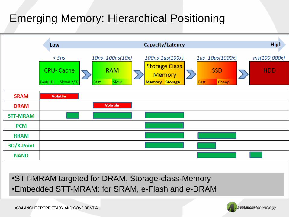
Emerging Memory: Hierarchical Positioning
•STT-MRAM targeted for DRAM, Storage-class-Memory
•Embedded STT-MRAM: for SRAM, e-Flash and e-DRAM
AVALANCHE PROPRIETARY AND CONFIDENTIAL AVALANCHE PROPRIETARY AND CONFIDENTIAL
Emerging Memory / Target Markets
• SRAM: Scaling below 20nm will cause increase cell size and leakage– L2/L3SRAM(embedded)
• STT-MRAM is the Leading candidate • Microprocessor, SOCs, Mobile SOC; Security applications; IOT
• DRAM: Scaling Challenge < 1Xnm – Stand alone and embedded • STT-RAM is the leading candidate
• Performance and low cost
• NOR Flash: Legacy; > $2B TAM
• STT-MRAM, ReRAM
AVALANCHE PROPRIETARY AND CONFIDENTIAL
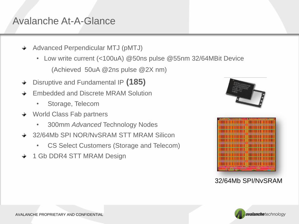
Avalanche At-A-Glance
32/64Mb SPI/NvSRAM
Advanced Perpendicular MTJ (pMTJ)
• Low write current (<100uA) @50ns pulse @55nm 32/64MBit Device
(Achieved 50uA @2ns pulse @2X nm)
Disruptive and Fundamental IP (185)
Embedded and Discrete MRAM Solution
• Storage, Telecom
World Class Fab partners
• 300mm Advanced Technology Nodes
32/64Mb SPI NOR/NvSRAM STT MRAM Silicon
• CS Select Customers (Storage and Telecom)
1 Gb DDR4 STT MRAM Design
AVALANCHE PROPRIETARY AND CONFIDENTIAL AVALANCHE PROPRIETARY AND CONFIDENTIAL
5
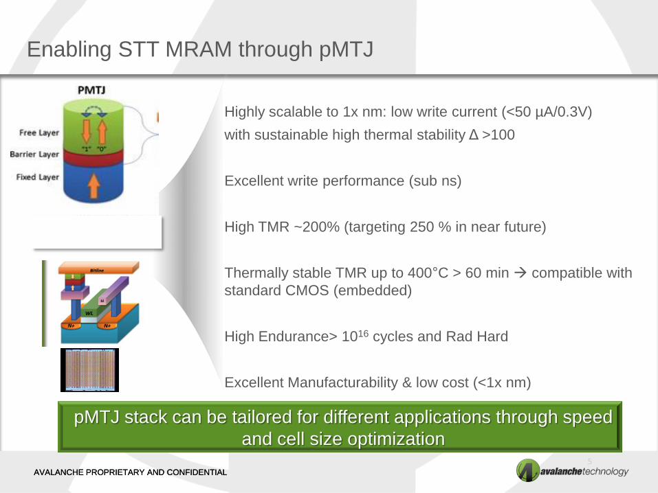
Highly scalable to 1x nm: low write current (<50 µA/0.3V)
with sustainable high thermal stability Δ >100
Excellent write performance (sub ns)
High TMR ~200% (targeting 250 % in near future)
•
Thermally stable TMR up to 400°C > 60 min compatible with
standard CMOS (embedded)
High Endurance> 1016 cycles and Rad Hard
Excellent Manufacturability & low cost (<1x nm)
pMTJ stack can be tailored for different applications through speed
and cell size optimization
Enabling STT MRAM through pMTJ
AVALANCHE PROPRIETARY AND CONFIDENTIAL AVALANCHE PROPRIETARY AND CONFIDENTIAL
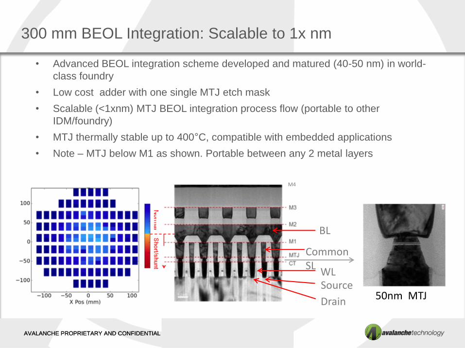
300 mm BEOL Integration: Scalable to 1x nm
• Advanced BEOL integration scheme developed and matured (40-50 nm) in world-
class foundry
• Low cost adder with one single MTJ etch mask
• Scalable (<1xnm) MTJ BEOL integration process flow (portable to other
IDM/foundry)
• MTJ thermally stable up to 400°C, compatible with embedded applications
• Note – MTJ below M1 as shown. Portable between any 2 metal layers
50nm MTJ
Common SL
BL
WL Source
Drain
M4
AVALANCHE PROPRIETARY AND CONFIDENTIAL AVALANCHE PROPRIETARY AND CONFIDENTIAL
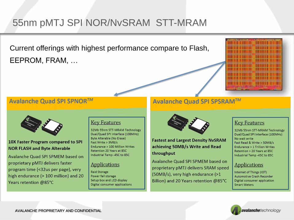
55nm pMTJ SPI NOR/NvSRAM STT-MRAM
Current offerings with highest performance compare to Flash,
EEPROM, FRAM, …
AVALANCHE PROPRIETARY AND CONFIDENTIAL
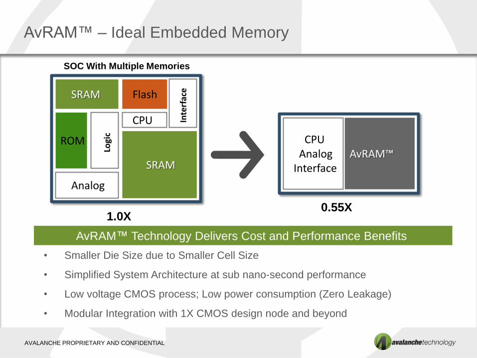
AvRAM™ – Ideal Embedded Memory
• Smaller Die Size due to Smaller Cell Size
• Simplified System Architecture at sub nano-second performance
• Low voltage CMOS process; Low power consumption (Zero Leakage)
• Modular Integration with 1X CMOS design node and beyond
1.0X
SOC With Multiple Memories
SRAM
ROM
Logi
c
CPU
Flash
SRAM
Inte
rfac
e Analog
0.55X
45% Die Size Saving
AvRAM™ CPU Analog Interface
AvRAM™ Technology Delivers Cost and Performance Benefits
AVALANCHE PROPRIETARY AND CONFIDENTIAL
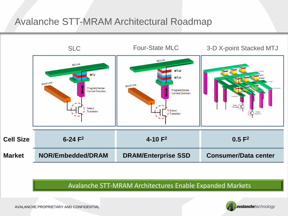
Avalanche STT-MRAM Architectural Roadmap
Cell Size 6-24 F2 4-10 F2 0.5 F2
Market NOR/Embedded/DRAM DRAM/Enterprise SSD Consumer/Data center
3-D X-point Stacked MTJ Four-State MLC SLC
Avalanche STT-MRAM Architectures Enable Expanded Markets
AVALANCHE PROPRIETARY AND CONFIDENTIAL
THANK YOU
10
46600 Landing Parkway – Fremont CA 94538 – T: 510| 897-3300 – F: 510| 438-0143 – www.Avalanche-Technology.com

SNIA NVM Summit Jan 20, 2016
Confidential Information
Private, VC funded, spinout from Freescale in 2008
Delivering our first generation MRAM products with 7 years of consecutive growth and 60M units shipped at 50% gross margin
Second generation product (Spin Torque) provides the opportunity for explosive growth. We are partnered with GLOBALFOUNDRIES to bring products on 300mm manufacturing to our customers
Establishing MRAM as the leading emerging memory technology
Everspin- The Only Company to Deliver MRAM
2
Confidential Information
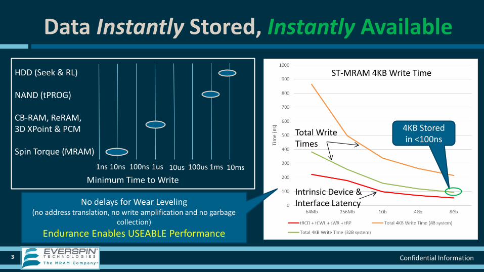
Data Instantly Stored, Instantly Available
3
Minimum Time to Write
10ns 100ns 1us 10us 100us 1ms 10ms 1ns
HDD (Seek & RL) NAND (tPROG) CB-RAM, ReRAM, 3D XPoint & PCM Spin Torque (MRAM)
Intrinsic Device & Interface Latency
ST-MRAM 4KB Write Time
Total Write Times
4KB Stored in <100ns
No delays for Wear Leveling (no address translation, no write amplification and no garbage
collection)
Endurance Enables USEABLE Performance
Confidential Information
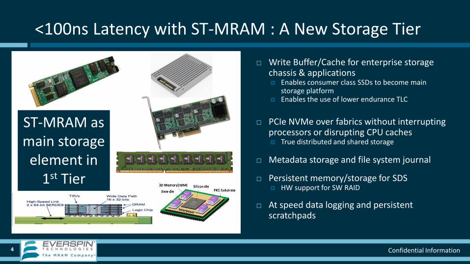
<100ns Latency with ST-MRAM : A New Storage Tier
4
Write Buffer/Cache for enterprise storage chassis & applications Enables consumer class SSDs to become main
storage platform Enables the use of lower endurance TLC
PCIe NVMe over fabrics without interrupting processors or disrupting CPU caches True distributed and shared storage
Metadata storage and file system journal
Persistent memory/storage for SDS HW support for SW RAID
At speed data logging and persistent scratchpads
ST-MRAM as main storage element in
1st Tier
Confidential Information
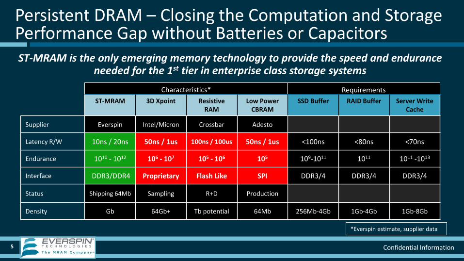
Characteristics* Requirements
5
ST-MRAM 3D Xpoint Resistive RAM
Low Power CBRAM
SSD Buffer RAID Buffer Server Write Cache
Supplier Everspin Intel/Micron Crossbar Adesto
Latency R/W 10ns / 20ns 50ns / 1us 100ns / 100us 50ns / 1us <100ns <80ns <70ns
Endurance 1010 - 1012 106 - 107 105 - 106 105 109-1011 1011 1011 -1013
Interface DDR3/DDR4 Proprietary Flash Like SPI DDR3/4 DDR3/4 DDR3/4
Status Shipping 64Mb Sampling R+D Production
Density Gb 64Gb+ Tb potential 64Mb 256Mb-4Gb 1Gb-4Gb 1Gb-8Gb
ST-MRAM is the only emerging memory technology to provide the speed and endurance needed for the 1st tier in enterprise class storage systems
Persistent DRAM – Closing the Computation and Storage Performance Gap without Batteries or Capacitors
*Everspin estimate, supplier data
Confidential Information
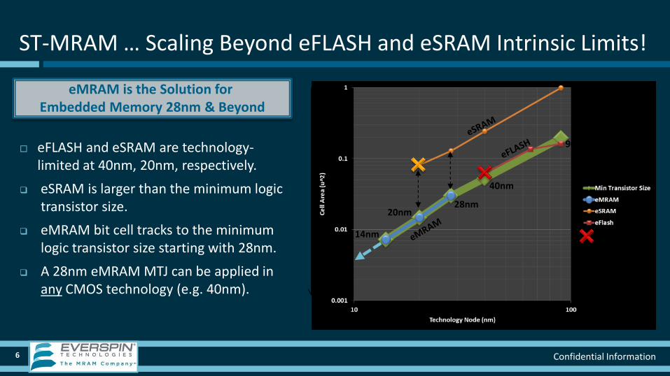
ST-MRAM … Scaling Beyond eFLASH and eSRAM Intrinsic Limits!
6
eFLASH and eSRAM are technology-limited at 40nm, 20nm, respectively.
eSRAM is larger than the minimum logic transistor size.
eMRAM bit cell tracks to the minimum logic transistor size starting with 28nm.
A 28nm eMRAM MTJ can be applied in any CMOS technology (e.g. 40nm).
90nm
40nm
28nm 20nm
14nm Intrinsic Limit
eSRAM Size over Min Transistor Size
eMRAM is the Solution for Embedded Memory 28nm & Beyond
Confidential Information
ST-MRAM is the Emerging Memory Ready to Use
MRAM production experience and know-how 300mm production with GLOBALFOUNDRIES = Quality and Quantity
Everspin branded products first targeted to enterprise storage Embedded MRAM for consumer, industrial, automotive and IOT SoC products
MRAM brings value as more than just memory Persistent DRAM in write intensive storage applications Versatility as embedded memory : Compute, Code, Capture all-in-one
Card-based MRAM to allow for early adoption via reference designs Ecosystem in place compatible with FPGAs and many controller IP products
Moving MRAM into the Mainstream
7

THANK YOU
SNIA NVM Summit Jan 20, 2016
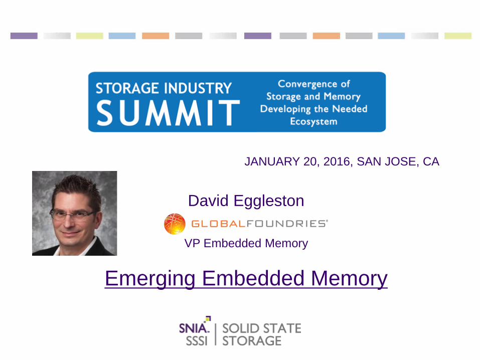
PRESENTATION TITLE GOES HERE David Eggleston
VP Embedded Memory
Emerging Embedded Memory
JANUARY 20, 2016, SAN JOSE, CA
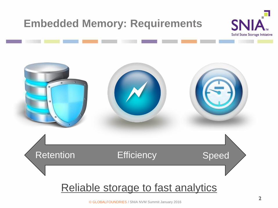
Embedded Memory: Requirements
Reliable storage to fast analytics
Speed Retention Efficiency
© GLOBALFOUNDRIES / SNIA NVM Summit January 2016 2
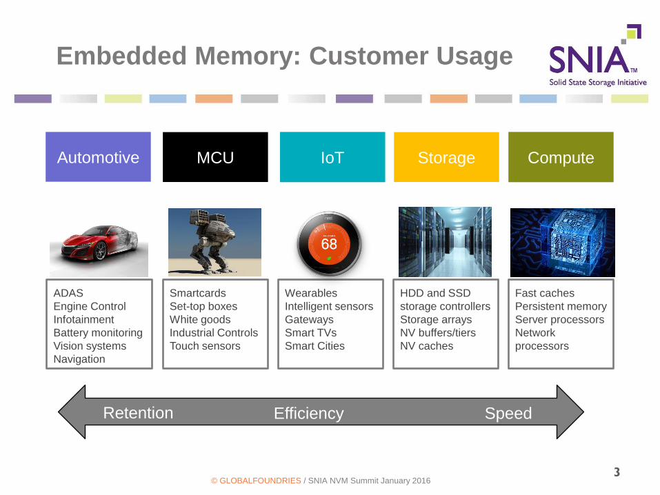
Embedded Memory: Customer Usage
Automotive IoT Compute MCU Storage
ADAS
Engine Control
Infotainment
Battery monitoring
Vision systems
Navigation
Smartcards
Set-top boxes
White goods
Industrial Controls
Touch sensors
Wearables
Intelligent sensors
Gateways
Smart TVs
Smart Cities
HDD and SSD
storage controllers
Storage arrays
NV buffers/tiers
NV caches
Fast caches
Persistent memory
Server processors
Network
processors
Speed Retention Efficiency
© GLOBALFOUNDRIES / SNIA NVM Summit January 2016 3
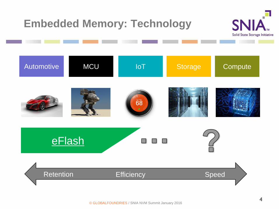
Embedded Memory: Technology
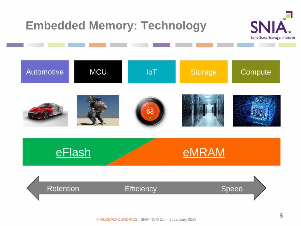
Automotive IoT Compute MCU Storage
Speed Retention Efficiency
eFlash
© GLOBALFOUNDRIES / SNIA NVM Summit January 2016 4
eMRAM eFlash
Embedded Memory: Technology
Automotive IoT Compute MCU Storage
Speed Retention Efficiency
© GLOBALFOUNDRIES / SNIA NVM Summit January 2016 5
eMRAM
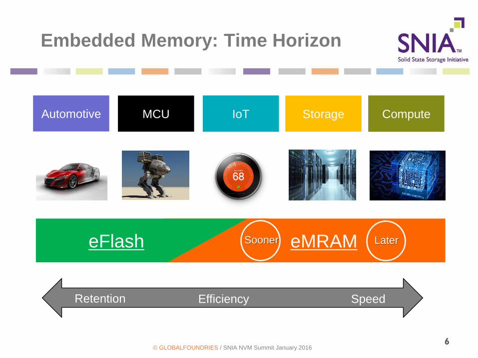
Embedded Memory: Time Horizon
Automotive IoT Compute MCU Storage
Speed Retention Efficiency
eFlash Sooner
© GLOBALFOUNDRIES / SNIA NVM Summit January 2016
Later
6
eMRAM
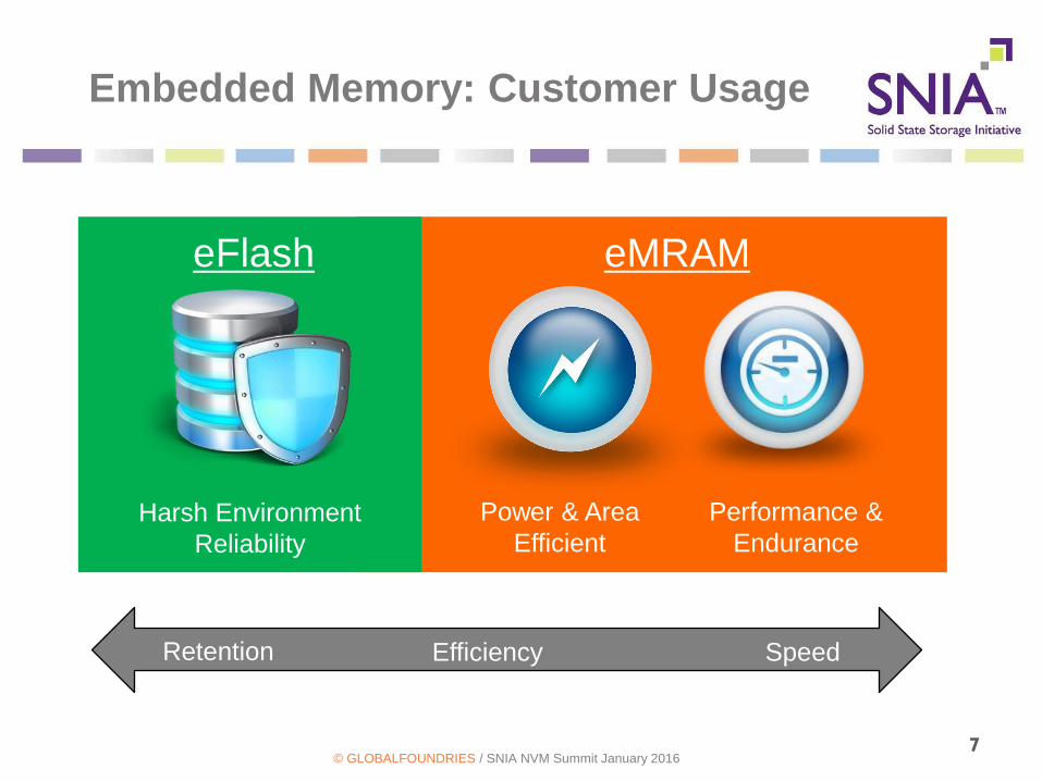
Embedded Memory: Customer Usage
Speed Retention Efficiency
eFlash
Harsh Environment
Reliability
Power & Area
Efficient
Performance &
Endurance
© GLOBALFOUNDRIES / SNIA NVM Summit January 2016 7
GLOBALFOUNDRIES Embedded Memory
Solving your product challenges for the
hyper-connected world.
© GLOBALFOUNDRIES / SNIA NVM Summit January 2016
8


