Page 1
EECS 247- Lecture 17 DAC Design (continued)- Nyquist Rate ADCs © 2007 H.K. Page 1
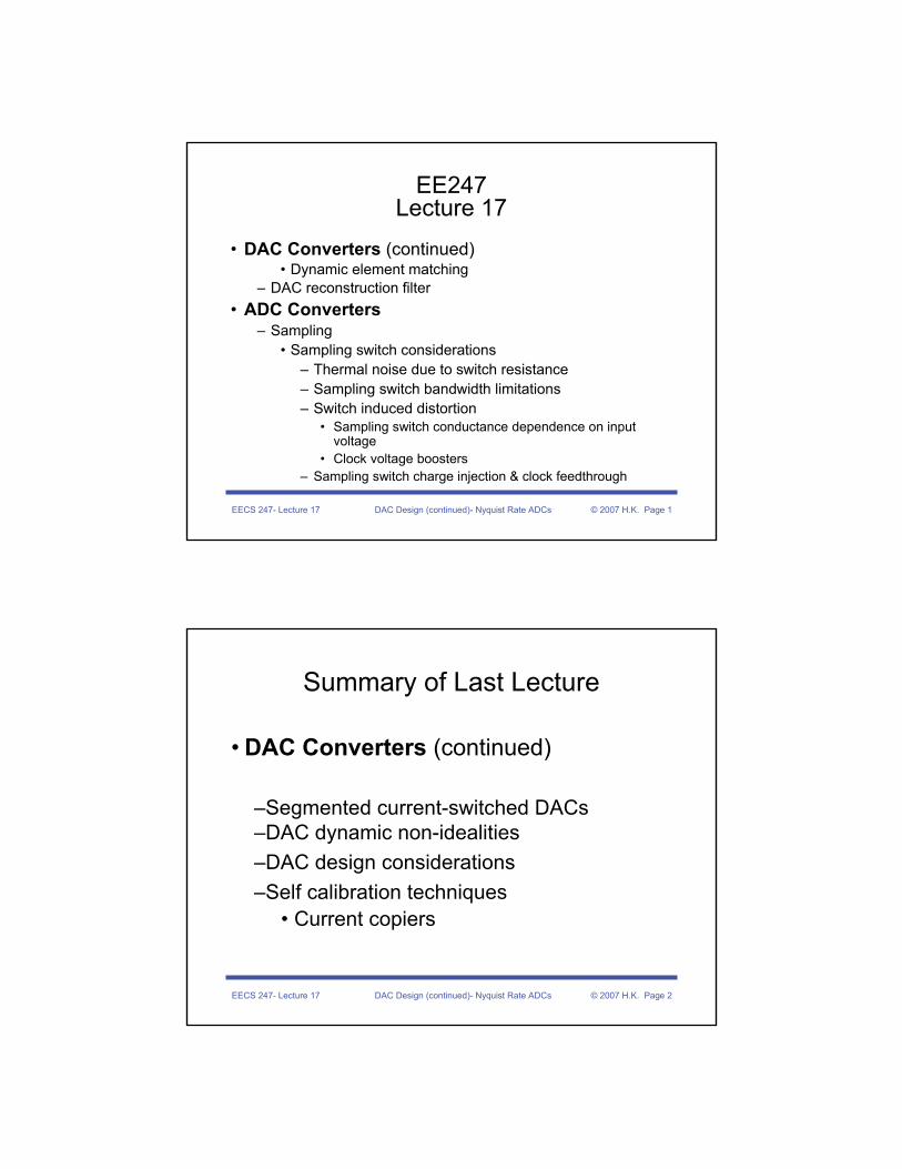
EE247Lecture 17
• DAC Converters (continued)• Dynamic element matching
– DAC reconstruction filter• ADC Converters
– Sampling• Sampling switch considerations
– Thermal noise due to switch resistance– Sampling switch bandwidth limitations– Switch induced distortion
• Sampling switch conductance dependence on input voltage
• Clock voltage boosters– Sampling switch charge injection & clock feedthrough
EECS 247- Lecture 17 DAC Design (continued)- Nyquist Rate ADCs © 2007 H.K. Page 2
Summary of Last Lecture
• DAC Converters (continued)
–Segmented current-switched DACs –DAC dynamic non-idealities–DAC design considerations–Self calibration techniques
• Current copiers
Page 2
EECS 247- Lecture 17 DAC Design (continued)- Nyquist Rate ADCs © 2007 H.K. Page 3
EECS 247- Lecture 17 DAC Design (continued)- Nyquist Rate ADCs © 2007 H.K. Page 4
I
I/2 I/2
Current Divider
16bit DAC (6+10)- MSB DAC uses calibrated current sources
Page 3
EECS 247- Lecture 17 DAC Design (continued)- Nyquist Rate ADCs © 2007 H.K. Page 5
I
I/2 I/2
Ideal Current Divider
Current Divider Inaccuracy due to Device Mismatch
I
I/2+dId /2
Real Current Divider
M1& M2 mismatched
I/2-dId /2
M1 M2M1 M2
Problem: Device mismatch could severely limit DAC accuracyUse of dynamic element matching (next few pages)
M1 & M2 mismatch results in the two output currents not being exactly equal:
d1 d2d
d d1 d2
d d
WLd
thWLd GS th
I II
2
dI I I
I I
ddI 2dV
I V V
+=
−=
⎡ ⎤⎛ ⎞= × +⎢ ⎥⎜ ⎟
− ⎝ ⎠⎣ ⎦
EECS 247- Lecture 17 DAC Design (continued)- Nyquist Rate ADCs © 2007 H.K. Page 6
Page 4
EECS 247- Lecture 17 DAC Design (continued)- Nyquist Rate ADCs © 2007 H.K. Page 7
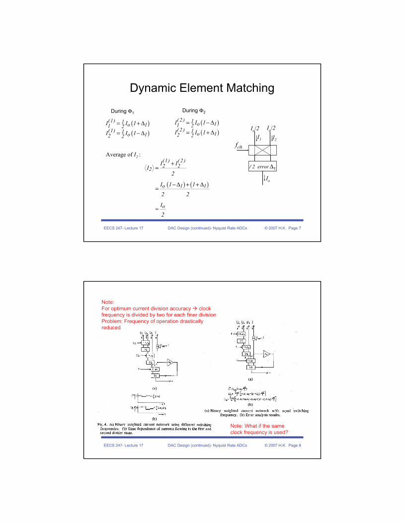
Dynamic Element Matching
( ) ( )
(1) ( 2 )2 22
1 1o
o
I II
2
1 1I2 2
I2
+=
− Δ + + Δ=
≈
( )( )
(1) 1 o 11 2(1) 1 o 12 2
I I 1
I I 1
= + Δ
= − Δ
/ 2 error Δ1
I1
During Φ1 During Φ2
I2fclk
Io
Io/2Io/2( )( )
( 2 ) 1 o 11 2( 2 ) 1 o 12 2
I I 1
I I 1
= − Δ
= + Δ
Average of I2 :
EECS 247- Lecture 17 DAC Design (continued)- Nyquist Rate ADCs © 2007 H.K. Page 8
Note: For optimum current division accuracy clock frequency is divided by two for each finer divisionProblem: Frequency of operation drastically reduced
Note: What if the same clock frequency is used?
Page 5
EECS 247- Lecture 17 DAC Design (continued)- Nyquist Rate ADCs © 2007 H.K. Page 9
Dynamic Element Matching
( )( )
( )( )( )214
1
2)1(
121)1(
3
121)1(
2
121)1(
1
111
1
1
Δ+Δ+=Δ+=
Δ−=
Δ+=
o
o
o
III
II
II ( )( )
( )( )( )214
1
2)2(
121)2(
3
121)2(
2
121)2(
1
111
1
1
Δ−Δ−=Δ−=
Δ+=
Δ−=
o
o
o
III
II
II
During Φ1 During Φ2
( )( ) ( )( )
( )21
2121
)2(3
)1(3
3
14
21111
4
2
ΔΔ+=
Δ−Δ−+Δ+Δ+=
+=
o
o
I
I
III
E.g. Δ1 = Δ2 = 1% matching error is (1%)2 = 0.01%
/ 2 error Δ1
I1
I2
fclk
Io
Io/2
/ 2 error Δ2
I3 I4
fclk
Io/4Io/4
EECS 247- Lecture 17 DAC Design (continued)- Nyquist Rate ADCs © 2007 H.K. Page 10
• Bipolar 12-bit DAC using dynamic element matching built in 1976• Element matching clock frequency 100kHz• INL <0.25LSB!
Page 6
EECS 247- Lecture 17 DAC Design (continued)- Nyquist Rate ADCs © 2007 H.K. Page 11
Example: State-of-the-Art current steering DAC
Segmented:6bit unit-element 8bit binary
EECS 247- Lecture 17 DAC Design (continued)- Nyquist Rate ADCs © 2007 H.K. Page 12
Page 7
EECS 247- Lecture 17 DAC Design (continued)- Nyquist Rate ADCs © 2007 H.K. Page 13
DAC In the Big Picture
• Learned to build DACs– Convert the
incoming digital signal to analog
• DAC output staircase form
• Some applications require filtering (smoothing) of DAC output
reconstruction filter
Analog Post processing
D/AConversion
DSP
A/D Conversion
Analog Preprocessing
Analog Input
Analog Output
000...001...
110
Anti-AliasingFilter
Sampling+Quantization
"Bits to Staircase"
Reconstruction Filter
EECS 247- Lecture 17 DAC Design (continued)- Nyquist Rate ADCs © 2007 H.K. Page 14
DAC Reconstruction Filter
• Need for and requirements depend on application
• Tasks:– Correct for sinx/x droop– Remove “aliases”
(stair-case approximation)
B fs/2
0 0.5 1 1.5 2 2.5 3
x 106
0
0.5
1
DAC
Inpu
t
0 0.5 1 1.5 2 2.5 3
x 106
0
0.5
1
Sin
x/x
0 0.5 1 1.5 2 2.5 30
0.5
1
DAC
Out
put
Normalized Frequency f/fs
Page 8
EECS 247- Lecture 17 DAC Design (continued)- Nyquist Rate ADCs © 2007 H.K. Page 15
Reconstruction Filter Options
• Reconstruction filter options:– Continuous-time filter only– CT + SC filter
• Digital and SC filter possible only in combination with oversampling (signal bandwidth B << fs/2)
• Digital filter– Band limits the input signal prevent aliasing– Could also provide high-frequency pre-emphasis to compensate in-
band sinx/x amplitude droop associated with the inherent DAC S/H function
DigitalFilter DAC SC
FilterCT
Filter
Reconstruction Filters
EECS 247- Lecture 17 DAC Design (continued)- Nyquist Rate ADCs © 2007 H.K. Page 16
DAC Reconstruction Filter Example: Voice-Band CODEC Receive Path
Ref: D. Senderowicz et. al, “A Family of Differential NMOS Analog Circuits for PCM Codec Filter Chip,”IEEE Journal of Solid-State Circuits, Vol.-SC-17, No. 6, pp.1014-1023, Dec. 1982.
Note: fsigmax = 3.4kHz
fsDAC = 8kHz
sin(π fsigmax x Ts )/(π fsig
max xTs )
= -2.75 dB droop due to DAC sinx/x shape
Receive Output
fs= 8kHz fs= 128kHzfs= 8kHz fs= 128kHz
fs= 128kHz
GSR
Reconstruction Filter& sinx/x Compensator
Page 9
EECS 247- Lecture 17 DAC Design (continued)- Nyquist Rate ADCs © 2007 H.K. Page 17
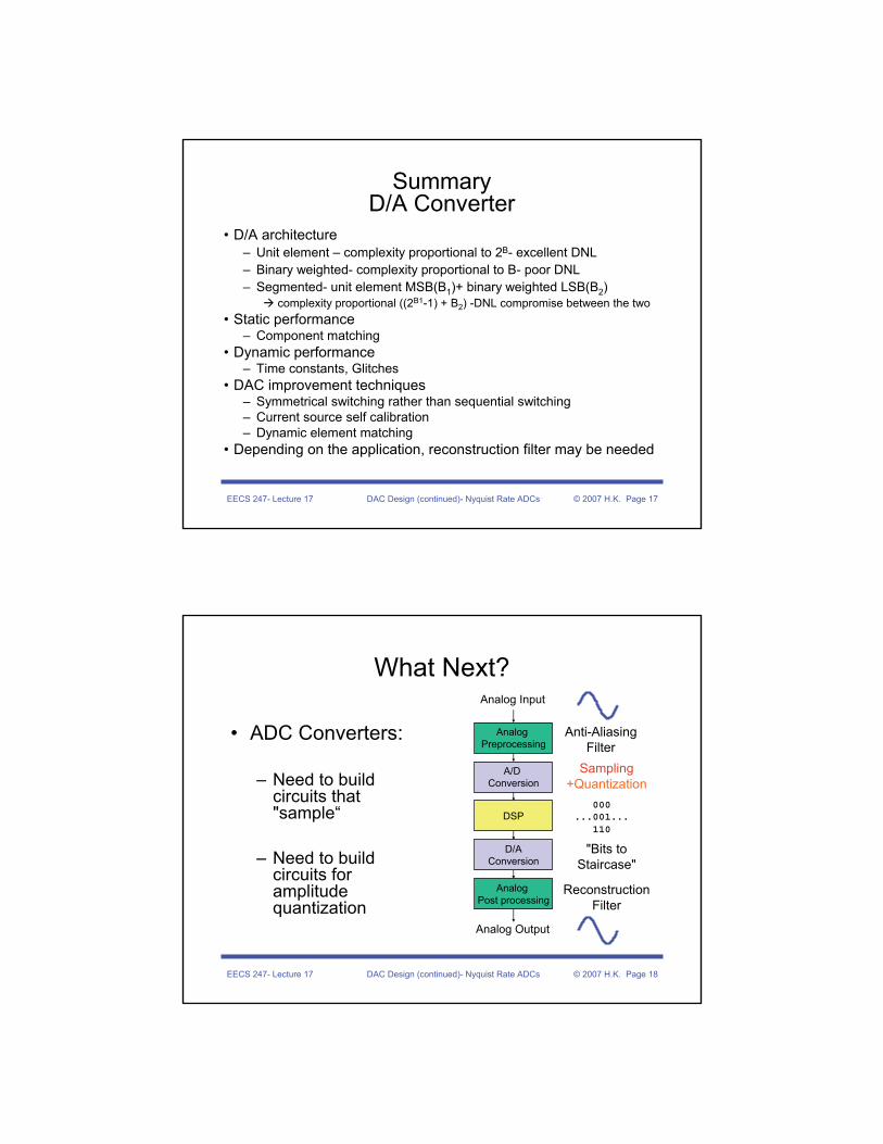
SummaryD/A Converter
• D/A architecture – Unit element – complexity proportional to 2B- excellent DNL – Binary weighted- complexity proportional to B- poor DNL– Segmented- unit element MSB(B1)+ binary weighted LSB(B2)
complexity proportional ((2B1-1) + B2) -DNL compromise between the two• Static performance
– Component matching• Dynamic performance
– Time constants, Glitches• DAC improvement techniques
– Symmetrical switching rather than sequential switching– Current source self calibration– Dynamic element matching
• Depending on the application, reconstruction filter may be needed
EECS 247- Lecture 17 DAC Design (continued)- Nyquist Rate ADCs © 2007 H.K. Page 18
What Next?
• ADC Converters:
– Need to build circuits that "sample“
– Need to build circuits for amplitude quantization
Analog Post processing
D/AConversion
DSP
A/D Conversion
Analog Preprocessing
Analog Input
Analog Output
000...001...
110
Anti-AliasingFilter
Sampling+Quantization
"Bits to Staircase"
Reconstruction Filter
Page 10
EECS 247- Lecture 17 DAC Design (continued)- Nyquist Rate ADCs © 2007 H.K. Page 19
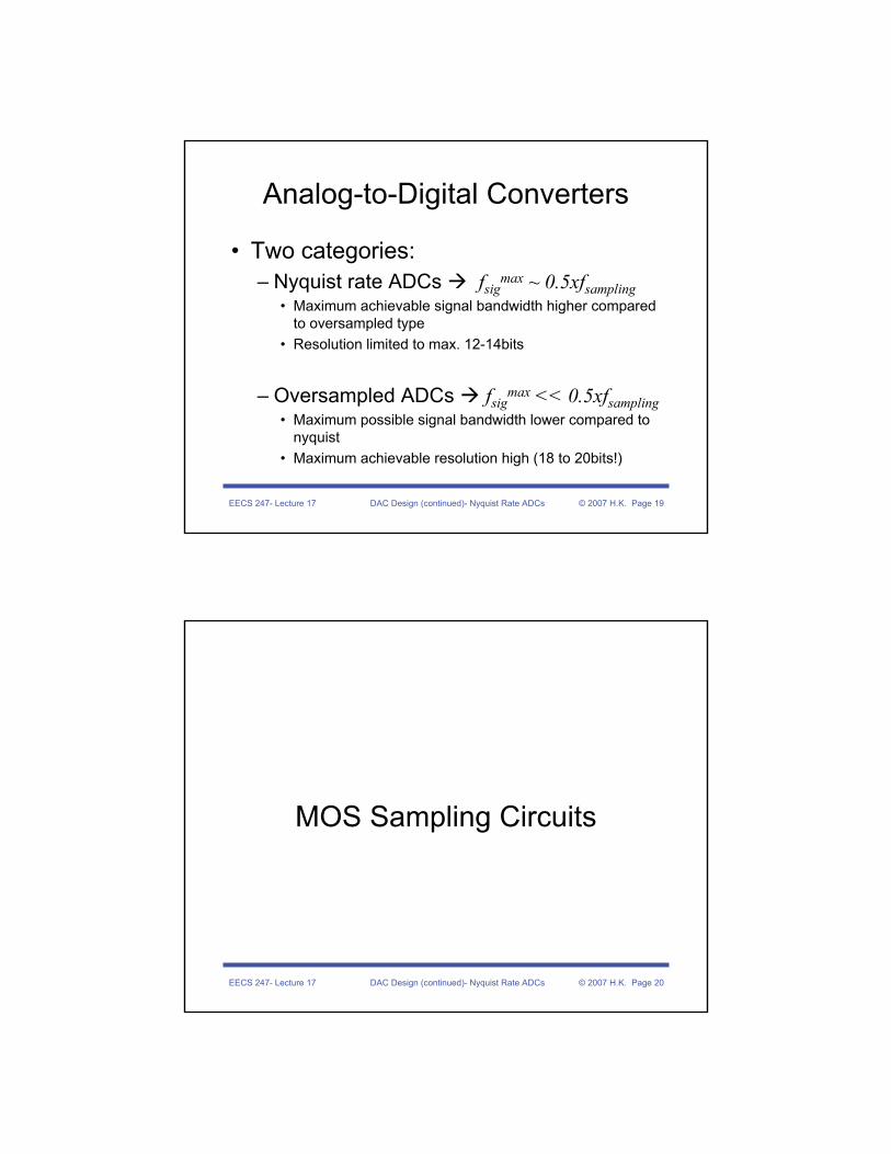
Analog-to-Digital Converters
• Two categories:– Nyquist rate ADCs fsig
max ~ 0.5xfsampling• Maximum achievable signal bandwidth higher compared
to oversampled type• Resolution limited to max. 12-14bits
– Oversampled ADCs fsigmax << 0.5xfsampling
• Maximum possible signal bandwidth lower compared to nyquist
• Maximum achievable resolution high (18 to 20bits!)
EECS 247- Lecture 17 DAC Design (continued)- Nyquist Rate ADCs © 2007 H.K. Page 20
MOS Sampling Circuits
Page 11
EECS 247- Lecture 17 DAC Design (continued)- Nyquist Rate ADCs © 2007 H.K. Page 21
Ideal Sampling• In an ideal world, zero
resistance sampling switches would close for the briefest instant to sample a continuous voltage vIN onto the capacitor C
Output Dirac-like pulses with amplitude equal to VINat the time of sampling
• In practice not realizable!
vIN vOUT
CS1
φ1
φ1
T=1/fS
EECS 247- Lecture 17 DAC Design (continued)- Nyquist Rate ADCs © 2007 H.K. Page 22
Ideal Track & Hold Sampling
vIN vOUT
CS1
φ1
• Vout tracks input for ½ clock cycle when switch is closed• Acquires exact value of Vin at the instant the switch opens• "Track and Hold" (T/H) (often called Sample & Hold!)
φ1
T=1/fS
Page 12
EECS 247- Lecture 17 DAC Design (continued)- Nyquist Rate ADCs © 2007 H.K. Page 23
Ideal T/H Sampling
ContinuousTime
T/H signal(Sampled-Data
Signal)
Clock
Discrete-TimeSignal
time
Trac
k
Hol
d
EECS 247- Lecture 17 DAC Design (continued)- Nyquist Rate ADCs © 2007 H.K. Page 24
Practical SamplingIssues
vIN vOUT
CM1
φ1
• Switch induced noise due to M1 finite channel resistance• Finite Rsw limited bandwidth finite acquisition time• Rsw = f(Vin) distortion• Switch charge injection & clock feedthrough• Clock jitter
Page 13
EECS 247- Lecture 17 DAC Design (continued)- Nyquist Rate ADCs © 2007 H.K. Page 25
kT/C Noise
• Switch resistance & sampling capacitor form a low-pass filter • Noise associated with the switch resistance results in Total noise
variance= kT/C @ the output (see noise analysis in Lecture 1)• In high resolution ADCs kT/C noise at times dominates overall
minimum signal handling capability (power dissipation considerations).
vIN vOUT
C
S1RvIN vOUT
CM1
φ1 4kTRΔf
EECS 247- Lecture 17 DAC Design (continued)- Nyquist Rate ADCs © 2007 H.K. Page 26
Sampling Network kT/C Noise
For ADCs sampling capacitor size is usually chosen based on having thermal noise smaller or equal or at times larger compared to quantization noise:Assumption: Nyquist rate ADC
2
2
2
2
2
212
1212
12
noise Q than equal)(or less is level noise thermalsuch that C Choose12
power noiseon quantizati Total :ADC rateNyquist aFor
FS
B
B
FS
B
B
B
VTkC
VTkC
CTk
×≥→
⎟⎟⎠
⎞⎜⎜⎝
⎛ −≥→
Δ≤
Δ≈
Page 14
EECS 247- Lecture 17 DAC Design (continued)- Nyquist Rate ADCs © 2007 H.K. Page 27
Sampling Network kT/C Noise
0.012 pF2.4 pF52 pF
824 pF211,200 pF
Cmin (VFS = 0.5V)
Required Cmin as a Function of ADC Resolution
0.003 pF0.8 pF13 pF
206 pF52,800 pF
812141620
Cmin (VFS = 1V)B
2
2212FS
BB
VTkC ≥
The large area required for C limit highest achievable resolution for Nyquist rate ADCs Oversampling results in reduction of required value for C (will be covered in oversampled converter lectures)
EECS 247- Lecture 17 DAC Design (continued)- Nyquist Rate ADCs © 2007 H.K. Page 28
Sampling Acquisition Bandwidth
• The resistance R of switch S1 turns the sampling network into a lowpass filter with finite time constant:
τ = RC
• Assuming Vin is constant during the sampling period and C is initially discharged
• Need to allow enough time for the output to settle to less than 1 ADC LSB determines minimum duration for φ1 or maximum clock frequency
vIN vOUT
CS1
φ1
R
( )τ/1)( tinout evtv −−=
φ1
vinvout
δv
Page 15
EECS 247- Lecture 17 DAC Design (continued)- Nyquist Rate ADCs © 2007 H.K. Page 29
Sampling: Effect of Switch On-Resistance
Example:B = 14, C = 13pF, fs = 100MHzTs /τ >> 19.4, or 10τ <<Ts/2 R << 40 Ω
φ1
T=1/fS
tx
( )
( )
( )
/
2
since 11
2 ln
Worst Case:
1 0.722 ln 2 1
1 1 0.722 ln 2 1
s
tx tx tin out out in
Ts
inin
in FS
s sB
Bs s
V V V V eTV e or
V
V V
T TB
Rf C B f C
τ
τ τ
τ
−
−
− << Δ = −
→ << Δ <<⎛ ⎞⎜ ⎟Δ⎝ ⎠
=
×<< ≈−
<< − ≈−
vIN vOUT
CS1
φ1
R
EECS 247- Lecture 17 DAC Design (continued)- Nyquist Rate ADCs © 2007 H.K. Page 30
Switch On-Resistance
( ) ( )
( )
( )( )
0
1,2
1 1
1Let us call @ =0
1
DS
D triodeDSD triode ox GS TH DS
ON DS V
ON
ox GS th ox DD th in
in o o
ox DD th
oON
in
DD th
dIVWI C V V VL R dV
R W WC V V C V V VL L
R V R then R WC V VL
RR VV V
μ
μ μ
μ
→
⎛ ⎞= − − ≅⎜ ⎟⎝ ⎠
= =− − −
=−
=− −
Switch MOS operating in triode mode:
Vin
CM1
φ1 VDDVGS =VDD - Vin
Page 16
EECS 247- Lecture 17 DAC Design (continued)- Nyquist Rate ADCs © 2007 H.K. Page 31
Sampling Distortion
in
DD th
outT V12 V V
in
v
v 1 e τ
⎛ ⎞− −⎜ ⎟⎜ ⎟−⎝ ⎠
=⎛ ⎞⎜ ⎟−⎜ ⎟⎜ ⎟⎝ ⎠
Simulated 10-Bit ADC &Ts/2 = 5τVDD – Vth = 2V VFS = 1VSampling Switch modeled:
Results in HD2=-41dBFS & HD3=-51.4dBFS
EECS 247- Lecture 17 DAC Design (continued)- Nyquist Rate ADCs © 2007 H.K. Page 32
Sampling Distortion
10bit ADC Ts/2 = 10 τVDD – Vth = 2V VFS = 1V
Doubling sampling time (or ½time constant)Results in:
HD2 improved from -41dBFS to -70dBFS ~30dB
HD3 improved from -51.4dBFS to -76.3dBFS ~25dB
Allowing enough time for the sampling network settling Reduces distortion due to switch R non-linear behavior to a tolerable level
Page 17
EECS 247- Lecture 17 DAC Design (continued)- Nyquist Rate ADCs © 2007 H.K. Page 33
Sampling DistortionEffect of Supply Voltage
10bit ADC & Ts/2 = 5τVDD – Vth = 2V VFS = 1V
• Effect of higher supply voltage on sampling distortionHD3 decrease by (VDD1/VDD2)2
HD2 decrease by (VDD1/VDD2)
10bit ADC & Ts/2 = 5τVDD – Vth = 4V VFS = 1V
EECS 247- Lecture 17 DAC Design (continued)- Nyquist Rate ADCs © 2007 H.K. Page 34
Sampling Distortion
10bit ADC Ts/τ = 20VDD – Vth = 2V VFS = 1V
• SFDR sensitive to sampling distortion - improve linearity by:
• Larger VDD /VFS• Higher sampling bandwidth
• Solutions:• Overdesign Larger switches
Issue: Increased switchcharge injectionIncreased nonlinear S &D junction cap.
• Maximize VDD/VFSDecreased dynamic range
if VDD const.• Complementary switch• Constant & max. VGS ≠ f(Vin)
Page 18
EECS 247- Lecture 17 DAC Design (continued)- Nyquist Rate ADCs © 2007 H.K. Page 35
Practical SamplingSummary So Far!
2
2212
B
BFS
C k TV
≥
( )1 for inON o o ox DD th
DD th
WVg g g C V VV V Lμ⎛ ⎞= − = −⎜ ⎟−⎝ ⎠
0.72
sR
B f C<<
• kT/C noise
• Finite Rsw limited bandwidth
• gsw = f (Vin) distortion
vINvOUT
CM1
φ1
EECS 247- Lecture 17 DAC Design (continued)- Nyquist Rate ADCs © 2007 H.K. Page 36
Sampling: Use of Complementary Switches
φ1φ1B
φ1
φ1B
gon
gop
goT =go
n + gopgo
•Complementary n & p switch advantages:Increase in the overall conductanceLinearize the switch conductance for the range |Vth
p|< Vin < Vdd -|Vthn|
Page 19
EECS 247- Lecture 17 DAC Design (continued)- Nyquist Rate ADCs © 2007 H.K. Page 37
Complementary Switch IssuesSupply Voltage Evolution
• Supply voltage has scaled down with technology scaling• Threshold voltages do not scale accordingly
Ref: A. Abo et al, “A 1.5-V, 10-bit, 14.3-MS/s CMOS Pipeline Analog-to-Digital Converter,” JSSC May 1999, pp. 599.
EECS 247- Lecture 17 DAC Design (continued)- Nyquist Rate ADCs © 2007 H.K. Page 38
Complementary SwitchEffect of Supply Voltage Scaling
gon
gop
goT =go
n + gopgeffective
•As supply voltage scales down input voltage range for constant go shrinksComplementary switch not effective when VDD becomes comparable to 2xVth
φ1φ1B
φ1
φ1B
Page 20
EECS 247- Lecture 17 DAC Design (continued)- Nyquist Rate ADCs © 2007 H.K. Page 39
Boosted & Constant VGS Sampling
VGS=const.
OFF ON
• Increase gate overdrive voltage as much as possible + keep VGSconstant
Switch overdrive voltage independent of signal level
Error due to finite RON linear (to 1st order)
Lower Ron lower time constant
• Gate voltage VGS =lowDevice offBeware of signal
feedthrough due to parasitic capacitors
EECS 247- Lecture 17 DAC Design (continued)- Nyquist Rate ADCs © 2007 H.K. Page 40
Constant VGS Sampling
(= voltage @ the switch input terminal)
Page 21
EECS 247- Lecture 17 DAC Design (continued)- Nyquist Rate ADCs © 2007 H.K. Page 41
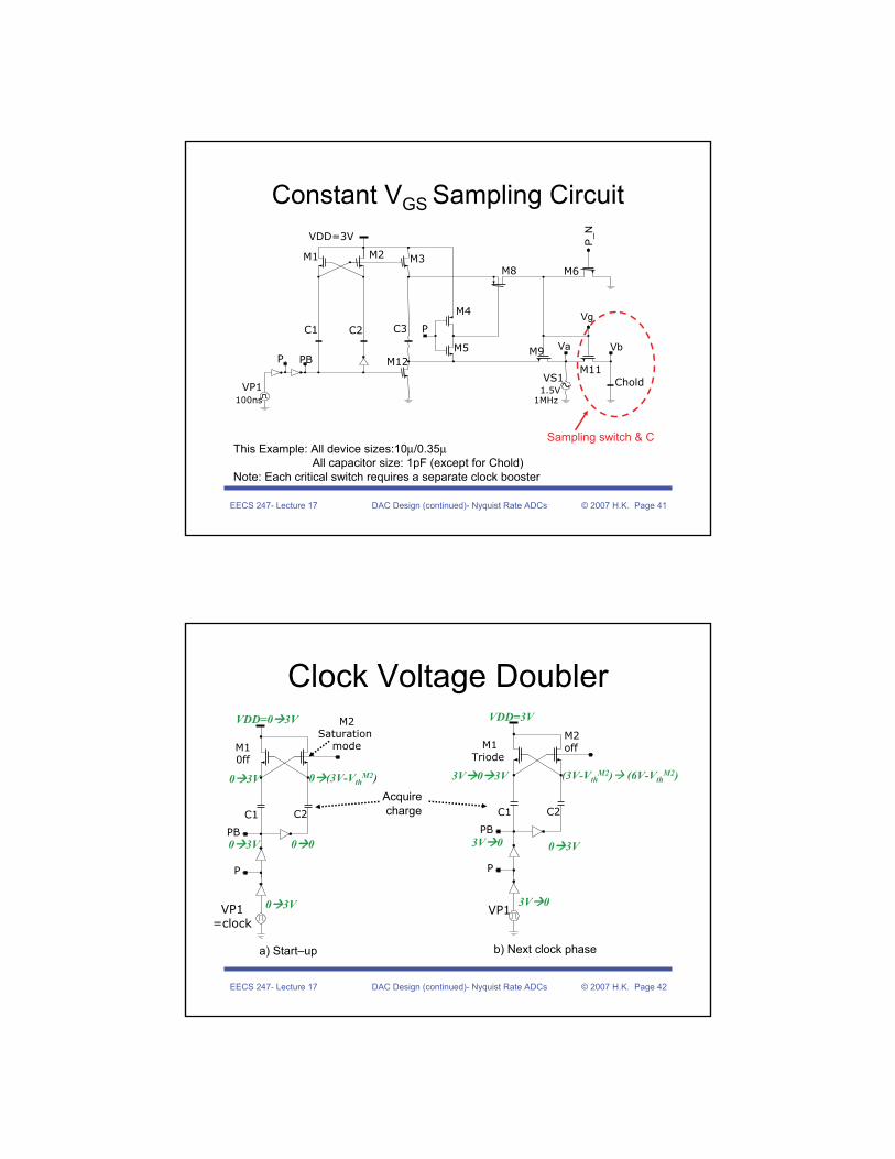
Constant VGS Sampling Circuit
VP1100ns
M12
M8
M9
M6
M11VS1
1.5V1MHz
Chold
P
C1 C2
M1 M2
VDD=3V
M3
C3
M5
M4
P
This Example: All device sizes:10μ/0.35μAll capacitor size: 1pF (except for Chold)
Note: Each critical switch requires a separate clock booster
P_N
Vg
Va Vb
Sampling switch & C
PB
EECS 247- Lecture 17 DAC Design (continued)- Nyquist Rate ADCs © 2007 H.K. Page 42
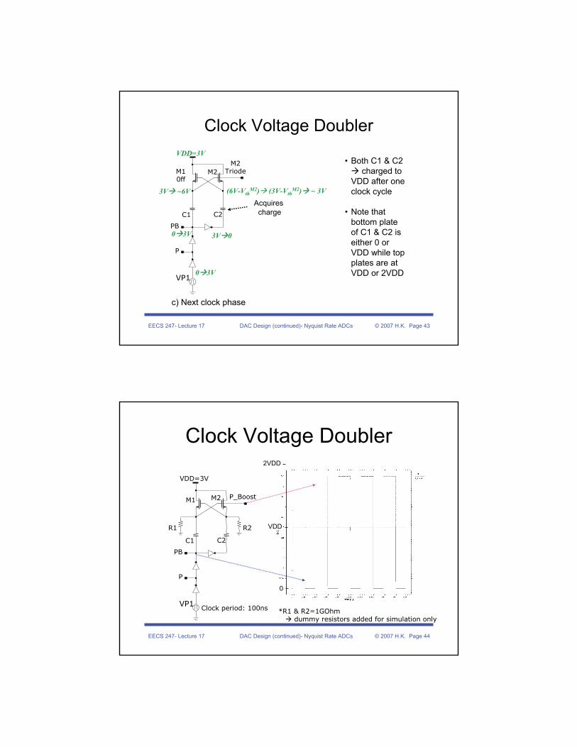
Clock Voltage Doubler
C1 C2
M10ff
M2Saturation
mode
VP1=clock
PB
VDD=0 3V
P
a) Start–up
0 3V
0 3V 0 0
0 3V 0 (3V-VthM2)
Acquire charge C1 C2
M1Triode
M2off
VP1
PB
VDD=3V
P
3V 0
3V 0
3V 0 3V (3V-VthM2) (6V-Vth
M2)
b) Next clock phase
0 3V
Page 22
EECS 247- Lecture 17 DAC Design (continued)- Nyquist Rate ADCs © 2007 H.K. Page 43
Clock Voltage Doubler
C1 C2
M10ff
M2
VP1
PB
VDD=3V
P
0 3V
0 3V
3V ~6V
3V 0
c) Next clock phase
(6V-VthM2) (3V-Vth
M2) ~ 3V
M2Triode
Acquires charge
• Both C1 & C2 charged to
VDD after one clock cycle
• Note that bottom plate of C1 & C2 is either 0 or VDD while top plates are at VDD or 2VDD
EECS 247- Lecture 17 DAC Design (continued)- Nyquist Rate ADCs © 2007 H.K. Page 44
Clock Voltage Doubler
C1 C2
M1 M2
VP1Clock period: 100ns
PB
P_Boost
VDD
2VDD
0
VDD=3V
R1 R2
*R1 & R2=1GOhmdummy resistors added for simulation only
P
Page 23
EECS 247- Lecture 17 DAC Design (continued)- Nyquist Rate ADCs © 2007 H.K. Page 45
Constant VGS Sampler: Φ Low
• Sampling switch M11 is OFF
• C3 charged to ~VDDInput voltage
source
M3Triode
C3
M12Triode
M4
OFF
VS11.5V1MHz
Chold1pF
~ 2 VDD(boosted clock)
VDD
VDD
OFF M11OFF
DeviceOFF
VDD=3V
EECS 247- Lecture 17 DAC Design (continued)- Nyquist Rate ADCs © 2007 H.K. Page 46
Constant VGS Sampler: Φ High
• C3 previously charged to VDD
• M8 & M9 are on:C3 across G-S of M11
• M11 on with constant VGS = VDD
C31pF
M8
M9 M11
VS11.5V1MHz
Chold1pF
VDD
Page 24
EECS 247- Lecture 17 DAC Design (continued)- Nyquist Rate ADCs © 2007 H.K. Page 47
Constant VGS Sampling
Input Switch VGate
Input Signal
Chold Signal
EECS 247- Lecture 17 DAC Design (continued)- Nyquist Rate ADCs © 2007 H.K. Page 48
Boosted Clock Sampling Complete Circuit
Ref: A. Abo et al, “A 1.5-V, 10-bit, 14.3-MS/s CMOS Pipeline Analog-to-Digital Converter,” JSSC May 1999, pp. 599.
Clock Multiplier
Switch
M7 & M13 for reliability
Remaining issues:
-VGS constant only for Vin <Vout
-Nonlinearity due to Vth dependence of M11on body-source voltage
Page 25
EECS 247- Lecture 17 DAC Design (continued)- Nyquist Rate ADCs © 2007 H.K. Page 49
Advanced Clock Boosting Technique
Ref: M. Waltari et al., "A self-calibrated pipeline ADC with 200MHz IF-sampling frontend," ISSCC 2002, Dig. Tech. Papers, pp. 314
Sampling Switch
EECS 247- Lecture 17 DAC Design (continued)- Nyquist Rate ADCs © 2007 H.K. Page 50
Advanced Clock Boosting Technique
• clk low– Capacitors C1a & C1b charged to VDD– MS off– Hold mode
Sampling Switch
clk low
Page 26
EECS 247- Lecture 17 DAC Design (continued)- Nyquist Rate ADCs © 2007 H.K. Page 51
Advanced Clock Boosting Technique
Sampling Switch
• clk high– Top plate of C1a & C1b connected to gate of sampling switch– Bottom plate of C1a connected to VIN– Bottom plate of C1b connected to VOUT– VGS & VGD of MS both @ VDD & ac signal on G of MS average of VIN &
VOUT
clk high
EECS 247- Lecture 17 DAC Design (continued)- Nyquist Rate ADCs © 2007 H.K. Page 52
Advanced Clock Boosting Technique
• Gate tracks average of input and output, reduces effect of I·R drop at high frequencies
• Bulk also tracks signal ⇒ reduced body effect (technology used allows connecting bulk to S)
• Reported measured SFDR = 76.5dB at fin=200MHz
Ref: M. Waltari et al., "A self-calibrated pipeline ADC with 200MHz IF-sampling frontend," ISSCC 2002, Dig. Tech. Papers, pp. 314
Sampling Switch
Page 27
EECS 247- Lecture 17 DAC Design (continued)- Nyquist Rate ADCs © 2007 H.K. Page 53
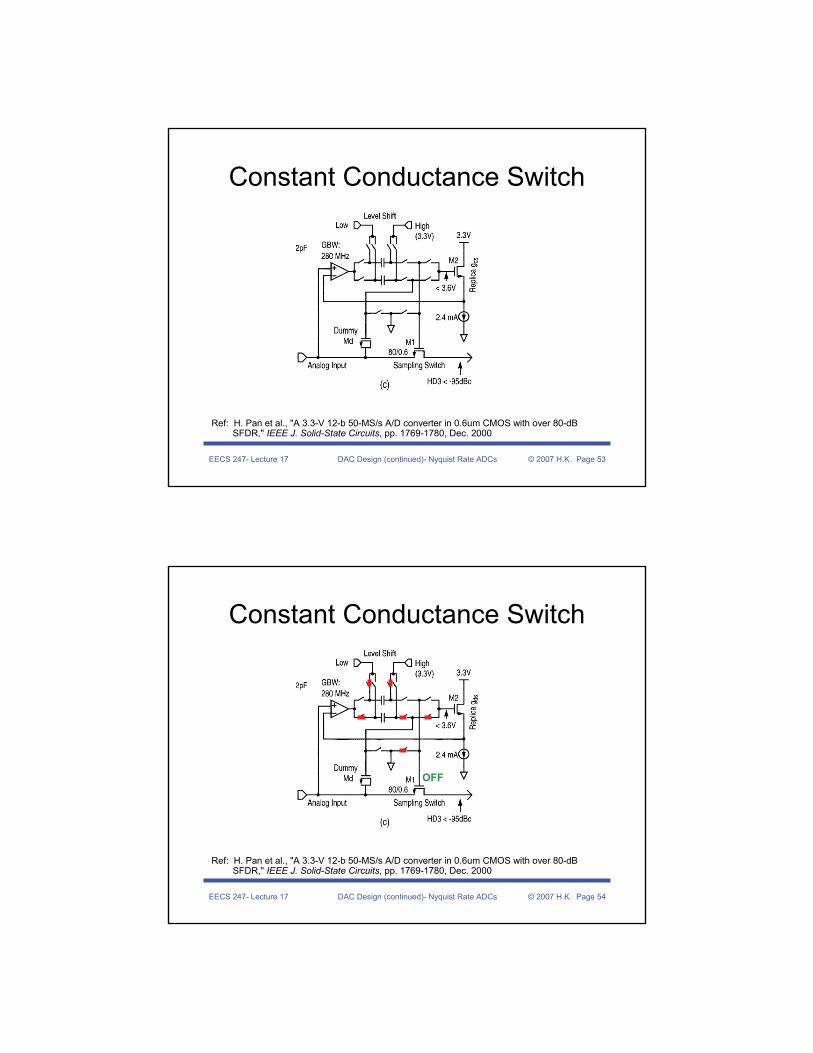
Constant Conductance Switch
Ref: H. Pan et al., "A 3.3-V 12-b 50-MS/s A/D converter in 0.6um CMOS with over 80-dB SFDR," IEEE J. Solid-State Circuits, pp. 1769-1780, Dec. 2000
EECS 247- Lecture 17 DAC Design (continued)- Nyquist Rate ADCs © 2007 H.K. Page 54
Constant Conductance Switch
Ref: H. Pan et al., "A 3.3-V 12-b 50-MS/s A/D converter in 0.6um CMOS with over 80-dB SFDR," IEEE J. Solid-State Circuits, pp. 1769-1780, Dec. 2000
OFF
Page 28
EECS 247- Lecture 17 DAC Design (continued)- Nyquist Rate ADCs © 2007 H.K. Page 55
Constant Conductance Switch
Ref: H. Pan et al., "A 3.3-V 12-b 50-MS/s A/D converter in 0.6um CMOS with over 80-dB SFDR," IEEE J. Solid-State Circuits, pp. 1769-1780, Dec. 2000
ON
M2 Constant currentconstant gds
M1 replica of M2 & same VGSas M2M1 alsoconstant gds
• Note: Authors report requirement of 280MHz GBW for the opamp for 12bit 50Ms/s ADC
• Also, opamp common-mode compliance for full input range required
EECS 247- Lecture 17 DAC Design (continued)- Nyquist Rate ADCs © 2007 H.K. Page 56
Switch Off-Mode Feedthrough Cancellation
Ref: M. Waltari et al., "A self-calibrated pipeline ADC with 200MHz IF-sampling frontend," ISSCC 2002, Dig. Techn. Papers, pp. 314
Page 29
EECS 247- Lecture 17 DAC Design (continued)- Nyquist Rate ADCs © 2007 H.K. Page 57
Practical Sampling
Vo
CM1
φ1
• Rsw = f(Vi) distortion• Switch charge injection & clock feedthrough
Vi
EECS 247- Lecture 17 DAC Design (continued)- Nyquist Rate ADCs © 2007 H.K. Page 58
Sampling Switch Charge Injection & Clock FeedthroughSwitching from Track to Hold
Vi VO
Cs
M1
VG
• First assume Vi is a DC voltage• When switch turns off offset voltage induced on Cs• Why?
VG
t
VH
Vi
VL
Vi +Vth
VO
Vi
toff
ΔV
t
Page 30
EECS 247- Lecture 17 DAC Design (continued)- Nyquist Rate ADCs © 2007 H.K. Page 59
SamplingSwitch Charge Injection
• Channel distributed RC network formed between G,S, and D• Channel to substrate junction capacitance distributed & voltage dependant• Drain/Source junction capacitors to substrate voltage dependant• Over-lap capacitance Cov = LDxWxCox
’ associated with G-S & G-D overlap
MOS xtor operating in triode regionCross section view
Distributed channel resistance & gate & junction capacitances
S
G
D
B
LD
L
Cov Cov
Cjdb
Cjsb
CHOLD
EECS 247- Lecture 17 DAC Design (continued)- Nyquist Rate ADCs © 2007 H.K. Page 60
Switch Charge Injection Slow Clock
• Slow clock clock fall time >> device speed During the period (t- to toff) current in channel discharges channel charge into low impedance signal source
• Only source of error Clock feedthrough from Cov to Cs
VG
t
VH
Vi
VL
Vi +Vth
tofft-
Device still conducting
Page 31
EECS 247- Lecture 17 DAC Design (continued)- Nyquist Rate ADCs © 2007 H.K. Page 61
Switch Clock Feedthrough Slow Clock
VG
t
VH
Vi
VL
Vi +Vth
VO
Vi
toff
ΔV
t
D
Cov
VG
( )
( )
( ) ( )
( )
( )
ovi th L
ov s
ovi th L
so i
ov ov ovo i i th L i th L
s s so i os
ov ovos th L
s s
CV V V V
C C
CV V V
CV V V
C C CV V V V V V 1 V V
C C CV V 1 V
C Cwhere ; V V V
C C
ε
ε
Δ = − + −+
≈ − + −
= + Δ⎛ ⎞
= − + − = − − −⎜ ⎟⎜ ⎟⎝ ⎠
= + +
= − = − −
t-
Cs
EECS 247- Lecture 17 DAC Design (continued)- Nyquist Rate ADCs © 2007 H.K. Page 62
Switch Charge Injection & Clock Feedthrough Slow Clock- Example
( )
' 2ov ox th L
ov
s
ovos th L
s
C 0.1 fF / C 9 fF / V 0.4V V 0
C 10 x0.1 fF /.1%
C 1pFAllowing 1/ 2LSB ADC resolut ion ~ 9bit
CV V V 0.4mV
C
μ μ
μ με
ε
= = = =
= − = − = −
= → <
= − − = −
VG
t
VH
Vi
VL
Vi +Vth
VO
Vi
toff
ΔV
t
Vi VO
Cs=1pF
M1
VG 10μ/0.18μ
t-