PAPER Special Section on Analog Circuit Techniques and Related Topics
A 6bit, 7mW, 700MS/s Subranging ADC using CDAC and Gate-Weighted Interpolation
Hyunui LEE †a), Student Member, Yusuke ASADA††, Nonmember, Masaya MIYAHARA †, Member, and Akira MATSUZAWA †, Fellow
SUMMARY A 6-bit, 7 mW, 700 MS/s subranging ADC using Capacitive DAC (CDAC) and gate-weighted interpolation fabricated in 90 nm CMOS technology is demonstrated. CDACs are used as a reference selection circuit instead of resistive DACs (RDAC) for reducing settling time and power dissipation. A gate-weighted interpolation scheme is also incorporated to the comparators, to reduce the circuit components, power dissipation and mismatch of conversion stages. By virtue of recent technology scaling, an interpolation can be realized in the saturation region with small error. A digital offset calibration technique using capacitor reduces comparator’s offset voltage from 10 mV to 1.5 mV per sigma. Experimental results show that the proposed ADC achieves a SNDR of 34 dB with calibration and FoM is 250 fJ/conv., which is very attractive as an embedded IP for low power SoCs. key words: Analog-to-digital converter (ADC), Capacitor DAC (CDAC), gate-weighted interpolation, digital offset calibration
1. Introduction
6 to 7-bit, several hundred MS/s to around 1 GS/s ADCs are required for disk drive front-ends, backplane and ultra-wideband receivers. Especially for embedded consumer SoCs, an ultra-low power operation is the most important characteristic rather than high resolution and high speed for the conventional ADC cores. This is because total power reduction is very crucial for portable applications and also for addressing green IT regulation.
Conventionally, the flash architecture has been used for these targets because of an advantage to high speed operation [1]. However, the flash architecture has an essential limitation in reducing conversion energy [2, 3]. An open-loop pipelined ADC has been investigated to attain this target [4], however the power dissipation is still large. The successive approximation register (SAR) architecture has been recognized as the most energy efficient architecture; however, it is not easy to increase the conversion rate up to the GS/s range [5, 6]. An asynchronous SAR ADC with interleaving [7] achieves a relatively high conversion rate but design difficulty is
increased. An extremely small FoM of 40 fJ/conv. steps has been attained in a 6-bit 2.2 GS/s ADC using dynamic pipeline architecture [8]. However, this ADC also introduced interleaving technique and the design becomes complicated.
The subranging architecture is a good solution for this target; however, the results have not been attractive. Although, [9] achieves 1 GS/s conversion rate, the power dissipation is very large due to pre-amplifiers which are introduced to reduce offset voltages. Another subranging ADC [10] achieves 8-bit resolution and 770 MS/s conversion rate; however, large power dissipation by pre-amplifiers and buffers are also problematic. A two-step architecture in [11] shows high resolution, but large power dissipation and low conversion speed reduces its attractiveness.
The work presented here is based on the subranging ADC using the CDAC, gate-weighted interpolation scheme, and digitally offset calibrated double-tail latched comparator [12, 13]. This paper is organized as follows: Section 2 introduces the ADC architecture, key schemes and techniques. Section 3 provides the implementation of the proposed ADC. Section 4 details the experimental results, and the paper is finally concluded in Section 5.
2. ADC Architecture and Techniques
2.1 Conventional Subranging Architecture
As introduced in Section 1, the subranging architecture is an attractive solution for our target specification. However, a conventional subranging architecture has a couple of issues, especially the disadvantage of the power dissipation.
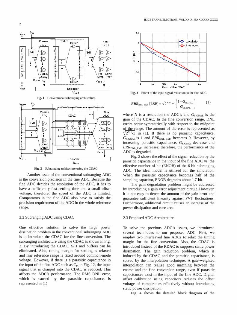
The conventional subranging architecture is shown in Fig. 1 [1]. There are two resistor ladders in the figure. Static current flows through the resistor ladder and this causes large power dissipation. This current can be suppressed by increasing resistance of the resistor ladder. However, reducing the current causes speed degradation, which is not suitable for high speed operation. The pre-amplifiers to reduce comparator’s offset are another source of the power dissipation. Furthermore, the buffers for the fine ADC consume static power.
Manuscript received January xx, 20xx. Manuscript revised March xx, 20xx. † The authors are with the Department of Physical
Electronics, Tokyo Institute of Technology, Tokyo, 152-8552 Japan.
†† The author is with Advantest Corporation, Gunma-ken, 370-0700 Japan
Another issue of the conventional subranging ADC is the conversion precision in the fine ADC. Because the fine ADC decides the resolution of the ADC, it has to have a sufficiently fast settling time and a small offset voltage; therefore, the speed of the ADC is limited. Comparators in the fine ADC also have to satisfy the precision requirement of the ADC in the whole reference range.
2.2 Subranging ADC using CDAC
One effective solution to solve the large power dissipation problem in the conventional subranging ADC is to introduce the CDAC for the fine conversion. The subranging architecture using the CDAC is shown in Fig. 2. By introducing the CDAC, S/H and buffers can be eliminated. Also, timing margin for settling is relaxed and fine reference range is fixed around common-mode voltage. However, if there is a parasitic capacitance in the input of the fine ADC such as CPI in Fig. 12, the input signal that is charged into the CDAC is reduced. This affects the ADC’s performance. The RMS DNL error, which is caused by the parasitic capacitance, is represented in (1)
−−= −
SIGNAL
SIGNAL1DNL_RMS
112]LSB[
GG
ERR N (1)
where N is a resolution the ADC’s and GSIGNAL is the gain of the CDAC. In the fine conversion range, DNL errors occur symmetrically with respect to the midpoint of the range. The amount of the error is represented as
2N-1-1 in (1). If there is no parasitic capacitance, GSIGNAL is 1 and ERRDNL_RMS becomes 0. However, by increasing parasitic capacitance, GSIGNAL decrease and ERRDNL_RMS increases; therefore, the performance of the ADC is degraded.
Fig. 3 shows the effect of the signal reduction by the parasitic capacitance in the input of the fine ADC vs. the effective number of bit (ENOB) of the 6-bit subranging ADC. The ideal model is utilized for the simulation. When the parasitic capacitance becomes half of the sampling capacitor, ENOB degrades about 1.7-bit.
The gain degradation problem might be addressed by introducing a gain error adjustment circuit. However, it is not easy to detect the amount of the gain error and guarantee sufficient linearity against PVT fluctuations. Furthermore, additional circuit causes an increase of the power dissipation and core area.
2.3 Proposed ADC Architecture
To solve the previous ADC’s issues, we introduced several techniques to our proposed ADC. First, we employ two interleaved fine ADCs to relax the timing margin for the fine conversion. Also, the CDAC is introduced instead of the RDAC to suppress static power dissipation. The gain reduction problem, which is induced by the CDAC and the parasitic capacitance, is solved by the interpolation technique. A gate-weighted interpolation can realize good matching between the coarse and the fine conversion range, even if parasitic capacitances exist in the input of the fine ADC. Digital offset calibration using capacitors reduces the offset voltage of comparators effectively without introducing static power dissipation.
Fig. 4 shows the detailed block diagram of the
Fig. 3 Effect of the input signal reduction in the fine ADC.
Fig. 1 Conventional subranging architecture.
Fig. 2 Subranging architecture using the CDAC.
IEICE TRANS. ELECTRON., VOL.XX-X, NO.X XXXX XXXX
3
proposed ADC. The coarse ADC consists of reference ladder, S/H, and 4×2-bit interpolation (IP) cells for 4-bit conversion. Each IP cell consists of 4 comparators that use gate-weighted interpolation technique. To realize the interpolation, the coarse ADC requires voltage shifter to generate two differential signal pairs because the input signal of the ADC is only one differential pair. In the coarse ADC, S/H circuit also performs voltage shifting. There is a resistor ladder in the coarse ADC. The total resistance of the resistor ladder is 1.7 kΩ. The resistor ladder consumes 0.3 mW power.
Two sets of the CDACs are used in the same way as in [11] to generate voltages for the fine conversion, instead of the conventional resistor ladder, in order to reduce the power dissipation and the settling time, simultaneously. Furthermore, these CDACs act as sample and hold circuits (S/H) like the CDAC in a SAR ADC.
The fine ADC consists of 9 comparators for 3-bit conversion which is illustrated as 3b IP cell in Fig. 4. These comparators mainly determine the resolution of the ADC; therefore, it is necessary to reduce their offset voltages. Digital offset calibration is incorporated to the comparator instead of the conventional method, such as a pre-amplifier, for low power dissipation. In Fig. 4, the CAL circuit and the digital memory blocks mean digital logic circuits and D flip-flops for the offset calibration. Two fine ADCs are interleaved to relax its operating frequency margin. Timing of each ADC is controlled by a clock timing controller. Conversion results from the coarse and the fine ADCs are gathered in digital logics and corrected using one redundancy bit.
Fig. 5 shows voltage transfer during conversion of the ADC. When the signal is applied to the ADC, the coarse ADC starts a conversion of 4-bit resolution. After
the coarse conversion, two sets of differential signals are outputted from the CDACs for interpolation according to the results of the coarse ADC. Finally, the fine ADC converts the input signal to the digital value in 3-bit resolution using the interpolation. The detailed explanation of the interpolation is shown in Section 2.4.
Fig. 6 shows a timing chart of the proposed ADC. The coarse ADC operates at the same speed as the sampling frequency; however, the fine ADCs operate at half of the conversion frequency to relax the requirement for the settling time and the timing margins. The fine ADC does not consume any power when it does not convert; therefore, the power dissipation does not increase although the circuit size is increased.
2.4 Interpolation
The proposed ADC addresses the gain reduction issue by using interpolation, which makes it possible to realize fine conversion without any reference voltages and to avoid the effect of the input parasitic capacitance of the fine conversion stages. To implement the interpolation, we introduce a gate-weighted interpolation scheme in the saturation region of MOS transistor to reduce the number of S/H circuits and input capacitance. The circuit implementation is described in Section 3.2.
Fig. 7 shows the 3-bit interpolation in the fine ADC of the proposed ADC. Two differential outputs from CDAC_a and CDAC_b are used to realize the interpolation. These output signals are shifted by 0.5 coarse LSB to realize one bit redundancy (half over range and half under range) for digital error correction [14].
Fig. 4 Proposed subranging ADC architecture.
Fig. 5 Conversion process of the proposed ADC. Fig. 6 Timing chart of the proposed ADC.
IEICE TRANS. ELECTRON., VOL.XX-X, NO.X XXXX XXXX
4
The interpolated voltages VPi and VNi in Fig. 7 can be represented as below
( )d
d
i
iVViV
2
2 INPbINPaP
+−= (2)
( )d
d
i
iVViV
2
2 INNbINNaN
+−= (3)
where d is a resolution of the interpolation, i is the number of the interpolated voltage, VINPa and VINNa are the differential output voltages from the CDAC_a and VINPb and VINNb are the differential voltages from the CDAC_b. For example, at the interpolation point 1 (between -2 and -1), conversion is executed by using only VP1 and VN1. The other conversions are also realized by the interpolated signals. Therefore, reference voltages are not required for the fine conversion and consistency between the coarse and the fine conversion range is realized automatically. Fig. 8 shows the effect of the gain reduction of the input signal for the fine ADC when using the interpolation. Even though the signal gain is reduced, as long as the reduction ratio of two differential signals is the same, the comparison point does not change. Therefore, the proposed ADC does not require a gain error correction circuit to solve this problem.
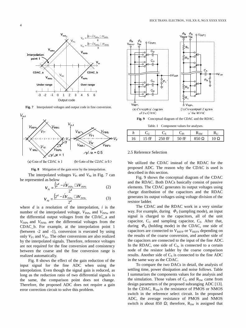
2.5 Reference Selection
We utilized the CDAC instead of the RDAC for the proposed ADC. The reason why the CDAC is used is described in this section.
Fig. 9 shows the conceptual diagram of the CDAC and the RDAC. Both DACs basically consist of passive elements. The CDAC generates its output voltages using charge distribution of the capacitors and the RDAC generates its output voltages using voltage division of the resistor ladder.
The CDAC and the RDAC work in a very similar way. For example, during ΦS (sampling mode), an input signal is charged to the capacitors, all of the unit capacitor, CU and sampling capacitor, CS. After that, during ΦH (holding mode) in the CDAC, one side of capacitors are connected to VREFP or VREFN depending on the results of the coarse conversion, and another side of the capacitors are connected to the input of the fine ADC. In the RDAC, one side of CS, is connected to a certain node of the resistor ladder by the coarse comparison results. Another side of CS is connected to the fine ADC in the same way as the CDAC.
To compare the two DACs in detail, the analysis of settling time, power dissipation and noise follows. Table I summarizes the components values for the analysis and the simulation. Those values of CU and RSW came from design parameters of the proposed subranging ADC [13]. In the CDAC, RSW is the resistance of PMOS or NMOS switch in the reference select circuit. In the proposed ADC, the average resistance of PMOS and NMOS switch is about 850 Ω; therefore, RSW is assigned that
0 1 2 3 4 5 6-1-2-3
VINPa
VINNa VINPb
VINNb
Vin
Vout
Output code
CDAC_a CDAC_b
( )8
8 INPbINPaP
iVViV i
+−=
( )8
8 INNbINNaN
iVViV i
+−=
VP1
VN1
Under range Over range
Fig. 7 Interpolated voltages and output code in fine conversion.
Fig. 8 Mitigation of the gain error by the interpolation.
Fig. 9 Conceptual diagram of the CDAC and the RDAC.
Table. I Component values for analyses.
h CU CS CPI RSW RU
16 15 fF 250 fF 50 fF 850 Ω 10 Ω
IEICE TRANS. ELECTRON., VOL.XX-X, NO.X XXXX XXXX
5
value. h is the number of unit capacitors (resistors). The total number of switches in both of the two DACs is 16, which is the same value as h. For the RDAC, CS is the sum of CU and RSW is same as the CDAC. CPI is parasitic capacitance of the subsequent circuit, such as the fine ADC. The value of CPI is assumed to be 50 fF which is estimated from the proposed fine ADC [13].
In the RDAC, another resistive component RU exists. Basically, the value of RU is decided for the optimal power dissipation and settling time with consideration of RSW. However, in this comparison, RSW is decided first by the CDAC. When using that value of RSW, even if RU is set to 0 Ω, the RDAC shows slower settling time than the CDAC. Although RU cannot influence the following comparison of the settling time, it affects the power dissipation and also settling time a little.
In this comparison, RU is assigned to 10 Ω. For values less than 10 Ω, the power dissipation of the RDAC increases drastically, but the settling time is only reduced by about 5 ps. More detail data is shown in section 2.5.2
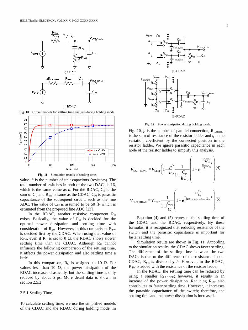
2.5.1 Settling Time
To calculate settling time, we use the simplified models of the CDAC and the RDAC during holding mode. In
Fig. 10, p is the number of parallel connection, RLADDER is the sum of resistance of the resistor ladder and q is the variation coefficient by the connected position in the resistor ladder. We ignore parasitic capacitance in each node of the resistor ladder to simplify this analysis.
−+
−=
+− t
h
h
e
hhp
VVPI
SW
U
PI
CR
C
C1
U
PISTEPOUT_CDAC 1
CC
1
11 (4)
( )
−+
= +
+− t
qeVV PISWLADDER
S
PI
CRR
C
C1
S
PISTEPOUT_RDAC 1
CC
1
1 (5)
Equation (4) and (5) represent the settling time of the CDAC and the RDAC, respectively. By these formulas, it is recognized that reducing resistance of the switch and the parasitic capacitance is important for faster settling time.
Simulation results are shown in Fig. 11. According to the simulation results, the CDAC shows faster settling. The difference of the settling time between the two DACs is due to the difference of the resistance. In the CDAC, RSW is divided by h. However, in the RDAC, RSW is added with the resistance of the resistor ladder.
In the RDAC, the settling time can be reduced by using a smaller RLADDER; however, it results in an increase of the power dissipation. Reducing RSW also contributes to faster settling time. However, it increases the parasitic capacitance of the switch; therefore, the settling time and the power dissipation is increased.
VINVREF
CS
CU
CU
VIN
SH
H
(a) CDAC
RU
RU
RU
(b) RDAC
VREF
CP_CDAC VOUT_CDAC
CPI
SH
H CPI
VOUT_RDAC
IC
IC
IR
IR
ILADDER
VREF+1
VREF
CP_CDAC
CP_RDAC
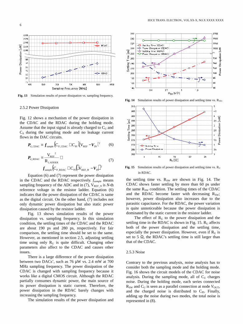
Fig. 12 Power dissipation during holding mode.
Fig. 10 Circuit models for settling time analysis during holding mode.
OUT[m
V]
Fig. 11 Simulation results of settling time.
IEICE TRANS. ELECTRON., VOL.XX-X, NO.X XXXX XXXX
6
2.5.2 Power Dissipation
Fig. 12 shows a mechanism of the power dissipation in the CDAC and the RDAC during the holding mode. Assume that the input signal is already charged to CU and CS during the sampling mode and no leakage current flows in the DAC circuits.
( )( )2INREFPIP_CDACsampled_CDAC VCC VfP −+= (6)
( )( )2INREF_PIP_RDACsample
LADDER
2REF
d_RDAC
VCC
R
V
Vf
P
N −+
+= (7)
Equation (6) and (7) represent the power dissipation in the CDAC and the RDAC respectively. fsample means sampling frequency of the ADC and in (7), VREF_N is N-th reference voltage in the resistor ladder. Equation (6) indicates that the power dissipation of the CDAC is same as the digital circuit. On the other hand, (7) includes not only dynamic power dissipation but also static power dissipation caused by the resistor ladder.
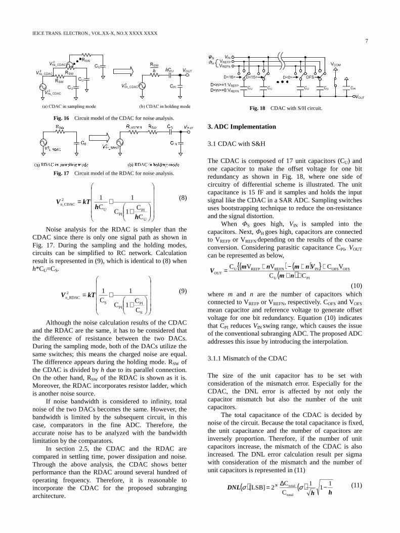
Fig. 13 shows simulation results of the power dissipation vs. sampling frequency. In this simulation condition, the settling times of the CDAC and the RDAC are about 190 ps and 280 ps, respectively. For fair comparison, the settling time should be set to the same. However, as mentioned in section 2.5, adjusting settling time using only RU is quite difficult. Changing other parameters also affect to the CDAC and causes other issues.
There is a large difference of the power dissipation between two DACs’, such as 76 µW vs. 2.4 mW at 700 MHz sampling frequency. The power dissipation of the CDAC is changed with sampling frequency because it works like a digital CMOS circuit. Although the RDAC partially consumes dynamic power, the main source of its power dissipation is static current. Therefore, the power dissipation in the RDAC barely changes with increasing the sampling frequency.
The simulation results of the power dissipation and
the settling time vs. RSW are shown in Fig. 14. The CDAC shows faster settling by more than 60 ps under the same RSW condition. The settling times of the CDAC and the RDAC become faster with decreasing RSW; however, power dissipation also increases due to the parasitic capacitance. For the RDAC, the power variation is quite unnoticeable because the power dissipation is dominated by the static current in the resistor ladder.
The effect of RU to the power dissipation and the settling time in the RDAC is shown in Fig. 15. RU affects both of the power dissipation and the settling time, especially the power dissipation. However, even if RU is set to 5 Ω, the RDAC’s settling time is still larger than that of the CDAC.
2.5.3 Noise
Contrary to the previous analysis, noise analysis has to consider both the sampling mode and the holding mode. Fig. 16 shows the circuit models of the CDAC for noise analysis. During the sampling mode, all of CU charges noise. During the holding mode, each series connected RSW and CU is seen as a parallel connection at node VOUT, and the charged noise is distributed to CPI. Finally, adding up the noise during two modes, the total noise is represented in (8).
Pow
er
Dis
sip
ation [
uW
]
Fig. 13 Simulation results of power dissipation vs. sampling frequency. Fig. 14 Simulation results of power dissipation and settling time vs. RSW.
Sett
ling
Tim
e [
ps]
Pow
er
Dis
sipation [
mW
]
Fig. 15 Simulation results of power dissipation and settling time vs. RU
in RDAC.
IEICE TRANS. ELECTRON., VOL.XX-X, NO.X XXXX XXXX
7
+
+=
U
PIPI
U
2n_CDAC
C
C1C
1
C
1
h
hkTV
(8)
Noise analysis for the RDAC is simpler than the CDAC since there is only one signal path as shown in Fig. 17. During the sampling and the holding modes, circuits can be simplified to RC network. Calculation result is represented in (9), which is identical to (8) when h*CU=CS.
+
+=
S
PIPI
S
2n_RDAC
C
C1C
1
C
1kTV
(9)
Although the noise calculation results of the CDAC and the RDAC are the same, it has to be considered that the difference of resistance between the two DACs. During the sampling mode, both of the DACs utilize the same switches; this means the charged noise are equal. The difference appears during the holding mode. RSW of the CDAC is divided by h due to its parallel connection. On the other hand, RSW of the RDAC is shown as it is. Moreover, the RDAC incorporates resistor ladder, which is another noise source.
If noise bandwidth is considered to infinity, total noise of the two DACs becomes the same. However, the bandwidth is limited by the subsequent circuit, in this case, comparators in the fine ADC. Therefore, the accurate noise has to be analyzed with the bandwidth limitation by the comparators.
In section 2.5, the CDAC and the RDAC are compared in settling time, power dissipation and noise. Through the above analysis, the CDAC shows better performance than the RDAC around several hundred of operating frequency. Therefore, it is reasonable to incorporate the CDAC for the proposed subranging architecture.
3. ADC Implementation
3.1 CDAC with S&H
The CDAC is composed of 17 unit capacitors (CU) and one capacitor to make the offset voltage for one bit redundancy as shown in Fig. 18, where one side of circuitry of differential scheme is illustrated. The unit capacitance is 15 fF and it samples and holds the input signal like the CDAC in a SAR ADC. Sampling switches uses bootstrapping technique to reduce the on-resistance and the signal distortion.
When ΦS goes high, VIN is sampled into the capacitors. Next, ΦH goes high, capacitors are connected to VREFP or VREFN depending on the results of the coarse conversion. Considering parasitic capacitance CPI, VOUT can be represented as below,
( ) ( ) ( ) PIU
OFSOFSINREFNREFPUOUT CC
VCVVC
++++−+=
nmVnmnm
V
(10) where m and n are the number of capacitors which connected to VREFP or VREFN, respectively. COFS and VOFS mean capacitor and reference voltage to generate offset voltage for one bit redundancy. Equation (10) indicates that CPI reduces VIN swing range, which causes the issue of the conventional subranging ADC. The proposed ADC addresses this issue by introducing the interpolation.
3.1.1 Mismatch of the CDAC
The size of the unit capacitor has to be set with consideration of the mismatch error. Especially for the CDAC, the DNL error is affected by not only the capacitor mismatch but also the number of the unit capacitors.
The total capacitance of the CDAC is decided by noise of the circuit. Because the total capacitance is fixed, the unit capacitance and the number of capacitors are inversely proportion. Therefore, if the number of unit capacitors increase, the mismatch of the CDAC is also increased. The DNL error calculation result per sigma with consideration of the mismatch and the number of unit capacitors is represented in (11)
( ) ( )hh
DNL N 11
1
C
C2]LSB[
total
total −∆= σσ (11)
VINVREFP
VREFN
D<16> D<15> D<0> OFS
CU CPI
VCOM
D<n>=1:VREFP
D<n>=0:VREFN
VOUT
S
H
CU CU CU
Fig. 18 CDAC with S/H circuit.
RSW
CU
(a) CDAC in sampling mode
RSW
CU
CURSW
CPI
VOUThCUh
(b) CDAC in holding mode
RSW
Vns_CDAC2
Vns_CDAC2
Vns_CDAC2
Vnh_CDAC2
Fig. 16 Circuit model of the CDAC for noise analysis.
Fig. 17 Circuit model of the RDAC for noise analysis.
IEICE TRANS. ELECTRON., VOL.XX-X, NO.X XXXX XXXX
8
where N is the resolution of the proposed ADC, Ctotal is the total capacitance of the CDAC, and h is the number of capacitors in the CDAC. When the unit capacitance is decreased, the mismatch error of the CDAC is increased with h. However, in the CDAC, the mismatch error is also suppressed by 1/h, because the signal range is divided by h. Finally, DNL error is reduced by about 1/ h. The calculation result of DNL(σ) is 0.011 LSB and the maximum INL(σ) derived from DNL(σ) is 0.03 LSB. Fig. 19 shows the maximum INL(σ) simulation results with 100 times iteration. Averaged the maximum INL(σ) is 0.0292 LSB, which shows good matching with the calculation. Target specifications of the INL & DNL are less than 0.25 LSB each; therefore, the CDAC satisfies the requirements with plenty of margin.
3.2 Comparator with Gate-Weighted Interpolation
The double-tail latched comparator with gate-weighted interpolation shown in Fig. 20 is employed in the proposed ADC. The comparator consists of 4 input MOS transistors for interpolation. The gate-weighted interpolation technique is very effective to reduce the power consumption. The interpolation method which is incorporated in [15] utilizes the on-conductance of a transistor in the linear region. In contrast, we realized the interpolation in the saturation region.
Drain current in the saturation region of a classical long channel MOS transistor exhibits a square-law relationship to (Vgs-VT) and causes non-linearity error when using an interpolation. However, the drain current of the recent scaled MOS transistor is proportional to (Vgs-VT) due to the heavy velocity saturation effect. The
drain current of the input transistor, ID, can be expressed as
( )'TgsD VVWI −≈ α (12)
where α is a coefficient, W is the gate width, and VT’ is the effective threshold voltage. We used the value of 290 mV as the VT’. In Fig. 20, current IP is the sum of the currents in MPa and MPb. Also, IN is the sum of the currents in MNa and MNb. The current IP is represented as below
( ) ( ) '' TINP_bPbTINP_aPaP VVWVVWI −+−= α (13)
where WPx means the gate width of the MOS transistor MPx. Equation (13) shows that IP can be controlled by changing gate width, WPx, even if the input voltages are not changed. The ratio between WPa and WPb is set by the ratio of the interpolation. The IN is also calculated in the same way. Comparators in each interpolating points compare using each IP and IN. This concept is shown in Fig. 7. The simulation results of the interpolation error using the same size of the input MOS transistor is shown in Fig. 21. The simulated interpolation range is assigned ±100mV from Vcom voltage. The interpolation error is less than 0.1 LSB when Vcom voltage is higher than 600 mV. Therefore, in those Vcom voltages, the gate-weighted interpolation can be realized with sufficient accuracy. However, it is difficult to realize the interpolation with Vcom of less than 500 mV, due to the increase of non-linearity.
3.3 Offset Calibration
An offset calibration technique by adjusting capacitance [16] is incorporated to the comparators in the fine ADC. 4-bit binary weighted PMOS varactors are used as voltage controlled capacitors. The gate size of a unit varactor is 200 nm x 100 nm.
Fig. 22 shows the calibration process. In Fig. 22, VCAL is the calibration voltage in the calibration logic and
Fig. 19 Simulation results of the maximum INL.
Fig. 20 Double-tail latched comparator with interpolation and offset
calibration.
Fig. 21 Simulation results of non-linearity error of MOS transistor.
IEICE TRANS. ELECTRON., VOL.XX-X, NO.X XXXX XXXX
9
VOFS is the offset voltage of the comparator. During calibration mode, all input nodes of the comparator are connected to the common voltage. Since all input nodes are the same, the output is determined by the offset voltage. Therefore, calibration logic changes the calibration code to cancel the offset voltage; as a result, VCAL gets closer to VOFS. When VCAL approaches to VOFS within voltage difference of one bit resolution of calibration, the calibration process is ended. After that, calibration code oscillates around the best calibration result. The comparator incorporates 4-bit calibration that operates at the same frequency as the clock resulting in a merely 16 clock cycles calibration process. The resolution of the calibration logic is about 2 mV, which is small enough for the 1/2 LSB (about 9 mV) of the proposed ADC,. The number of bit for calibration is determined by Monte Carlo simulation.
The Monte Carlo simulation results show that large mismatch of about 10 mV(σ) can be suppressed to 0.9 mV(σ) with calibration. The propagation delay with calibration at the input drive voltage of 1 mV is 140 ps and consumed energy for one conversion is 63 fJ/conv.. The input referred noise voltage is about 0.7 mV per sigma of which value is reduced to 64% for the comparator without offset calibration. The increase of node capacitance reduces input referred noise voltage.
3.3.1 Offset Calibration at each Interpolating Point
The introduced offset calibration technique adjusts the slew rate at the VOP_1st, VON_1st nodes in Fig. 20. This slew rate is affected by not only capacitance at the nodes of the VOP_1st and VON_1st but also by the input common-mode voltage. During the calibration mode, all of the comparators are using the same input common-mode voltage. However, in the operation mode, each comparator has a different interpolating ratio, this also means that the input common-mode voltage of each comparator is different. This results in the difference of slew rate between the calibration mode and the operation mode. Therefore, it is necessary to verify that this offset calibration method is effective to reduce the offset voltage for each interpolating point with different input common-mode voltage.
To examine the effect of input common-mode voltage, we introduced variation of Veff against variation of the capacitance at the output nodes such as VOP_1st and VON_1st. The result is shown in (14).
o_1sto_1st 2C
V
C
V effoff −=∂∂ (14)
where Voff is the offset of the comparator, Veff is (Vgs-V t) of the input MOS transistor and Co_1st is the capacitance at the output nodes of VOP_1st and VON_1st. Equation (14) shows the variation of the offset voltage is proportional to Veff; therefore, it is effective to reduce Veff to achieve more accurate offset calibration.
The 1000 times Monte Carlo simulation results of input referred offset voltage after calibration at each interpolating point for 3 common-mode voltages are shown in Fig. 23. The simulation results show that the offset calibration is effective for all interpolation ratios even if the common-mode voltage is changed from 500 mV to 600 mV. This means that the variation of the slew rate is small enough.
4. Experimental Results
The proposed ADC has been fabricated in a 90 nm CMOS technology. Fig. 24 shows the chip micro-photograph and the layout of the ADC, which occupies an active area of 0.13 mm2.
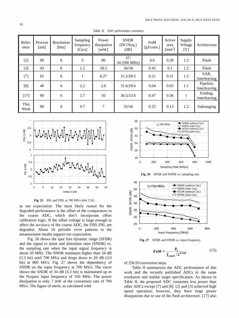
Fig. 25 shows the measured DNL and INL at the conversion rate of 700 MS/s after the offset calibration. The DNL is less than +/‐0.6 LSB and the INL is less than +/‐0.8 LSB. The DNL/INL results are not as good
Input
Refe
rred
Offset
Voltage
(σ
) [m
V]
Fig. 23 Input referred offset voltage after calibration at each
interpolating point.
Fig. 24 Chip micrograph and layout.
Fig. 22 Process of the offset voltage calibration.
IEICE TRANS. ELECTRON., VOL.XX-X, NO.X XXXX XXXX
10
as our expectation. The most likely reason for the degraded performance is the offset of the comparators in the coarse ADC, which don’t incorporate offset calibration logic. If the offset voltage is large enough to affect the accuracy of the coarse ADC, the DNL/INL are degraded. About 16 periodic error patterns in the measurement results support our expectation.
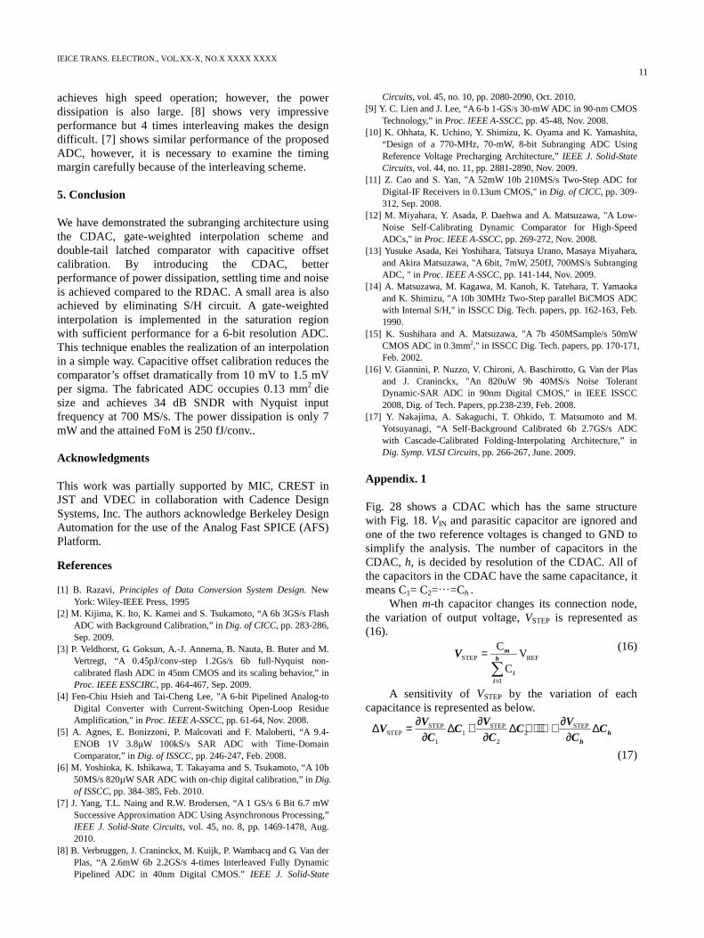
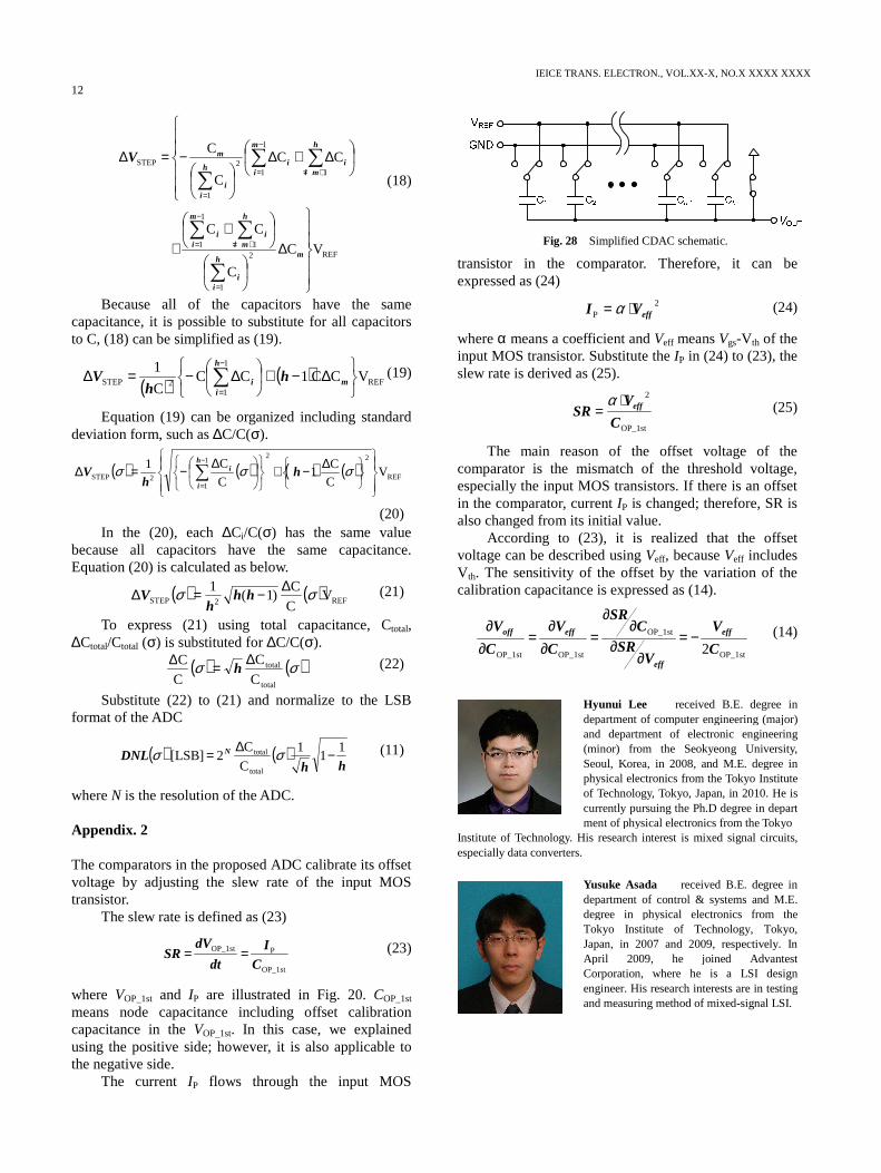
Fig. 26 shows the spur free dynamic range (SFDR) and the signal to noise and distortion ratio (SNDR) vs. the sampling rate when the input signal frequency is about 50 MHz. The SNDR maintains higher than 34 dB (5.3 bit) until 700 MS/s and drops down to 20 dB (3.0 bit) at 800 MS/s. Fig. 27 shows the dependency of SNDR on the input frequency at 700 MS/s. The curve shows the SNDR of 34 dB (5.3 bit) is maintained up to the Nyquist input frequency of 350 MHz. The power dissipation is only 7 mW at the conversion rate of 700 MS/s. The figure of merit, as calculated with
ENOBsample
d
fP
FoM2⋅
= (15)
of 250 fJ/conversion steps. Table II summarizes the ADC performance of this
work and the recently published ADCs in the same resolution and similar target specification. As shown in Table II, the proposed ADC consumes less power than other ADCs except [7] and [8]. [2] and [3] achieved high speed operation; however, they have large power dissipations due to use of the flash architecture. [17] also
achieves high speed operation; however, the power dissipation is also large. [8] shows very impressive performance but 4 times interleaving makes the design difficult. [7] shows similar performance of the proposed ADC, however, it is necessary to examine the timing margin carefully because of the interleaving scheme.
5. Conclusion
We have demonstrated the subranging architecture using the CDAC, gate-weighted interpolation scheme and double-tail latched comparator with capacitive offset calibration. By introducing the CDAC, better performance of power dissipation, settling time and noise is achieved compared to the RDAC. A small area is also achieved by eliminating S/H circuit. A gate-weighted interpolation is implemented in the saturation region with sufficient performance for a 6-bit resolution ADC. This technique enables the realization of an interpolation in a simple way. Capacitive offset calibration reduces the comparator’s offset dramatically from 10 mV to 1.5 mV per sigma. The fabricated ADC occupies 0.13 mm2 die size and achieves 34 dB SNDR with Nyquist input frequency at 700 MS/s. The power dissipation is only 7 mW and the attained FoM is 250 fJ/conv..
Acknowledgments
This work was partially supported by MIC, CREST in JST and VDEC in collaboration with Cadence Design Systems, Inc. The authors acknowledge Berkeley Design Automation for the use of the Analog Fast SPICE (AFS) Platform.
References
[1] B. Razavi, Principles of Data Conversion System Design. New York: Wiley-IEEE Press, 1995
[2] M. Kijima, K. Ito, K. Kamei and S. Tsukamoto, “A 6b 3GS/s Flash ADC with Background Calibration,” in Dig. of CICC, pp. 283-286, Sep. 2009.
[3] P. Veldhorst, G. Goksun, A.-J. Annema, B. Nauta, B. Buter and M. Vertregt, “A 0.45pJ/conv-step 1.2Gs/s 6b full-Nyquist non-calibrated flash ADC in 45nm CMOS and its scaling behavior,” in Proc. IEEE ESSCIRC, pp. 464-467, Sep. 2009.
[4] Fen-Chiu Hsieh and Tai-Cheng Lee, "A 6-bit Pipelined Analog-to Digital Converter with Current-Switching Open-Loop Residue Amplification," in Proc. IEEE A-SSCC, pp. 61-64, Nov. 2008.
[5] A. Agnes, E. Bonizzoni, P. Malcovati and F. Maloberti, “A 9.4-ENOB 1V 3.8µW 100kS/s SAR ADC with Time-Domain Comparator,” in Dig. of ISSCC, pp. 246-247, Feb. 2008.
[6] M. Yoshioka, K. Ishikawa, T. Takayama and S. Tsukamoto, “A 10b 50MS/s 820µW SAR ADC with on-chip digital calibration,” in Dig. of ISSCC, pp. 384-385, Feb. 2010.
[7] J. Yang, T.L. Naing and R.W. Brodersen, “A 1 GS/s 6 Bit 6.7 mW Successive Approximation ADC Using Asynchronous Processing,” IEEE J. Solid-State Circuits, vol. 45, no. 8, pp. 1469-1478, Aug. 2010.
[8] B. Verbruggen, J. Craninckx, M. Kuijk, P. Wambacq and G. Van der Plas, “A 2.6mW 6b 2.2GS/s 4-times Interleaved Fully Dynamic Pipelined ADC in 40nm Digital CMOS.” IEEE J. Solid-State
Circuits, vol. 45, no. 10, pp. 2080-2090, Oct. 2010. [9] Y. C. Lien and J. Lee, “A 6-b 1-GS/s 30-mW ADC in 90-nm CMOS
Technology,” in Proc. IEEE A-SSCC, pp. 45-48, Nov. 2008. [10] K. Ohhata, K. Uchino, Y. Shimizu, K. Oyama and K. Yamashita,
“Design of a 770-MHz, 70-mW, 8-bit Subranging ADC Using Reference Voltage Precharging Architecture,” IEEE J. Solid-State Circuits, vol. 44, no. 11, pp. 2881-2890, Nov. 2009.
[11] Z. Cao and S. Yan, "A 52mW 10b 210MS/s Two-Step ADC for Digital-IF Receivers in 0.13um CMOS," in Dig. of CICC, pp. 309-312, Sep. 2008.
[12] M. Miyahara, Y. Asada, P. Daehwa and A. Matsuzawa, "A Low-Noise Self-Calibrating Dynamic Comparator for High-Speed ADCs," in Proc. IEEE A-SSCC, pp. 269-272, Nov. 2008.
[13] Yusuke Asada, Kei Yoshihara, Tatsuya Urano, Masaya Miyahara, and Akira Matsuzawa, "A 6bit, 7mW, 250fJ, 700MS/s Subranging ADC, " in Proc. IEEE A-SSCC, pp. 141-144, Nov. 2009.
[14] A. Matsuzawa, M. Kagawa, M. Kanoh, K. Tatehara, T. Yamaoka and K. Shimizu, "A 10b 30MHz Two-Step parallel BiCMOS ADC with Internal S/H," in ISSCC Dig. Tech. papers, pp. 162-163, Feb. 1990.
[15] K. Sushihara and A. Matsuzawa, "A 7b 450MSample/s 50mW CMOS ADC in 0.3mm2," in ISSCC Dig. Tech. papers, pp. 170-171, Feb. 2002.
[16] V. Giannini, P. Nuzzo, V. Chironi, A. Baschirotto, G. Van der Plas and J. Craninckx, "An 820uW 9b 40MS/s Noise Tolerant Dynamic-SAR ADC in 90nm Digital CMOS," in IEEE ISSCC 2008, Dig. of Tech. Papers, pp.238-239, Feb. 2008.
[17] Y. Nakajima, A. Sakaguchi, T. Ohkido, T. Matsumoto and M. Yotsuyanagi, “A Self-Background Calibrated 6b 2.7GS/s ADC with Cascade-Calibrated Folding-Interpolating Architecture,” in Dig. Symp. VLSI Circuits, pp. 266-267, June. 2009.
Appendix. 1
Fig. 28 shows a CDAC which has the same structure with Fig. 18. VIN and parasitic capacitor are ignored and one of the two reference voltages is changed to GND to simplify the analysis. The number of capacitors in the CDAC, h, is decided by resolution of the CDAC. All of the capacitors in the CDAC have the same capacitance, it means C1= C2=…=Ch . When m-th capacitor changes its connection node, the variation of output voltage, VSTEP is represented as (16).
REF
1
STEP VC
C
∑=
= h
ii
mV (16)
A sensitivity of VSTEP by the variation of each capacitance is represented as below.
hh
CC
VC
CV
CC
VV ∆
∂∂+⋅⋅⋅+∆
∂∂+∆
∂∂=∆ STEP
22
STEP1
1
STEPSTEP
(17)
IEICE TRANS. ELECTRON., VOL.XX-X, NO.X XXXX XXXX
12
REF2
1
1
1
1
1
1
12
1
STEP
VC
C
CC
CC
C
C
∆
++
∆+∆
−=∆
∑
∑∑
∑∑
∑
=
+=
−
=
+=
−
=
=
mh
ii
h
mii
m
ii
h
mii
m
ii
h
ii
mV
(18)
Because all of the capacitors have the same capacitance, it is possible to substitute for all capacitors to C, (18) can be simplified as (19).
( ) ( ) REF
1
12STEP VCC1CC
C
1
∆−+
∆−=∆ ∑−
=m
h
ii h
hV (19)
Equation (19) can be organized including standard deviation form, such as ∆C/C(σ).
( ) ( ) ( ) ( ) REF
221
12STEP V
C
C1
C
C1
∆−+
∆−=∆ ∑−
=
σσσ hh
Vh
i
i
(20) In the (20), each ∆Ci/C(σ) has the same value because all capacitors have the same capacitance. Equation (20) is calculated as below.
( ) ( ) REF2STEP VC
C)1(
1 σσ ∆−=∆ hhh
V (21)
To express (21) using total capacitance, Ctotal, ∆Ctotal/Ctotal (σ) is substituted for ∆C/C(σ).
( ) ( )σσtotal
total
C
C
CC ∆=∆
h (22)
Substitute (22) to (21) and normalize to the LSB format of the ADC
( ) ( )hh
DNL N 11
1
C
C2]LSB[
total
total −∆= σσ (11)
where N is the resolution of the ADC.
Appendix. 2
The comparators in the proposed ADC calibrate its offset voltage by adjusting the slew rate of the input MOS transistor. The slew rate is defined as (23)
OP_1st
POP_1st
CI
dt
dVSR == (23)
where VOP_1st and IP are illustrated in Fig. 20. COP_1st means node capacitance including offset calibration capacitance in the VOP_1st. In this case, we explained using the positive side; however, it is also applicable to the negative side. The current IP flows through the input MOS
transistor in the comparator. Therefore, it can be expressed as (24)
2P effVI ⋅= α (24)
where α means a coefficient and Veff means Vgs-V th of the input MOS transistor. Substitute the IP in (24) to (23), the slew rate is derived as (25).
OP_1st
2
C
VSR eff⋅
=α (25)
The main reason of the offset voltage of the comparator is the mismatch of the threshold voltage, especially the input MOS transistors. If there is an offset in the comparator, current IP is changed; therefore, SR is also changed from its initial value. According to (23), it is realized that the offset voltage can be described using Veff, because Veff includes V th. The sensitivity of the offset by the variation of the calibration capacitance is expressed as (14).
OP_1st
OP_1st
OP_1stOP_1st 2C
V
VSR
CSR
C
V
C
V eff
eff
effoff −=∂
∂∂
∂=
∂∂
=∂∂ (14)
Hyunui Lee received B.E. degree in department of computer engineering (major) and department of electronic engineering (minor) from the Seokyeong University, Seoul, Korea, in 2008, and M.E. degree in physical electronics from the Tokyo Institute of Technology, Tokyo, Japan, in 2010. He is currently pursuing the Ph.D degree in depart ment of physical electronics from the Tokyo
Institute of Technology. His research interest is mixed signal circuits, especially data converters.
Yusuke Asada received B.E. degree in department of control & systems and M.E. degree in physical electronics from the Tokyo Institute of Technology, Tokyo, Japan, in 2007 and 2009, respectively. In April 2009, he joined Advantest Corporation, where he is a LSI design engineer. His research interests are in testing and measuring method of mixed-signal LSI.
Fig. 28 Simplified CDAC schematic.
IEICE TRANS. ELECTRON., VOL.XX-X, NO.X XXXX XXXX
13
Masaya Miyahara received B.E. degree in Mechanical & Electrical Engineering from Kisarazu National College of Technology, Kisarazu, Japan, in 2004, and M.E. and Ph.D. degree in Physical Electronics from Tokyo Institute of Technology, Tokyo, Japan, in 2006 and 2009 respectively. Since 2009, he has been an Assistant Professor at Department of Physical Electronics, Tokyo Institute of Technology, Tokyo, Japan. His research interests are RF CMOS and Mixed
signal circuits.
Akira Matsuzawa received B.S., M.S., and Ph. D. degrees in electronics engineering from Tohoku University, Sendai, Japan, in 1976, 1978, and 1997 respectively. In 1978, he joined Matsushita Electric Industrial Co. Ltd. Since then, he has been working on research and development of analog and Mixed Signal LSI technologies; ultra-high speed ADCs, intelligent CMOS sensors, RF CMOS circuits, and digital read-channel technologies for DVD systems. From 1997
to 2003, he was a general manager in advanced LSI technology development center. On April 2003, he joined Tokyo Institute of Technology and he is a professor on physical electronics. Currently he is researching in mixed signal technologies; CMOS wireless transceiver, RF CMOS circuit design for SDR and high-speed data converters. He served the guest editor in chief for special issue on analog LSI technology of IEICE transactions on electronics in 1992, 1997, and 2003, committee member for analog technology in ISSCC, IEEE SSCS elected Adcom from 2005 to 2008, and IEEE SSCS Distinguished lecturer. He received the IR100 award in 1983, the R&D100 award and the remarkable invention award in 1994, and the ISSCC evening panel award in 2003 and 2005. He is an IEEE Fellow since 2002 and an IEICE Fellow since 2010.