09/11/2010 1 Synthetic Processes of Nanomaterials Dr Montree Sawangphruk (DPhil) Chemical Engineering, Kasetsart University, Room #1209-5, email:[email protected]http://pirun.ku.ac.th/~fengmrs/ Outline Introduction Formation of Clusters and Nanoparticles from a Supersaturated Vapour Techniques for Cluster Formation Scaling Laws Nanoparticles and Films Produced by Sputtering and Thermal Evaporation and Laser Methods Chemical vapour deposition (CVD) Physical Vapour Deposition (PVD) Atomic Layer Deposition (ALD) Molecular Beam Epitaxy (MBE) Top-down approach Grinding/Milling Lithography Bottom-up approach (Wet Chemistry) Sol-gel process Electrochemical deposition Homework! (a 2-page report)
Transcript
09/11/2010
1
Synthetic Processes of Nanomaterials
Dr Montree Sawangphruk (DPhil)
Chemical Engineering, Kasetsart University, Room #1209-5, email:[email protected]
http://pirun.ku.ac.th/~fengmrs/
Outline
Introduction
Formation of Clusters and
Nanoparticles from a
Supersaturated Vapour
Techniques for Cluster
Formation
Scaling Laws
Nanoparticles and Films Produced
by Sputtering and Thermal
Evaporation and Laser Methods
Chemical vapour deposition
(CVD)
Physical Vapour Deposition
(PVD)
Atomic Layer Deposition (ALD)
Molecular Beam Epitaxy (MBE)
Top-down approach
Grinding/Milling
Lithography
Bottom-up approach (Wet
Chemistry)
Sol-gel process
Electrochemical deposition
Homework! (a 2-page report)
09/11/2010
2
Formation of Clusters and Nanoparticles
from a Supersaturated Vapor
The sizes of the nanoparticles made by these techniques
cover the entire range from dimers to nanoparticles
which are ≤100 nm in diameter.
The term cluster, as used here, is mainly reserved for
smaller nanoparticles containing fewer than 104 atoms or
molecules.
09/11/2010
3
Classical Nucleation Theory for Cluster
Formation
Nucleation of new particles from a continuous phase can
occur heterogeneously or homogeneously.
Heterogeneous nucleation from a vapour phase can
occur on foreign nuclei or dust particles, ions or surfaces.
Homogeneous nucleation occurs in the absence of any
foreign particles or ions when the vapour molecules
condense to form embryonic droplets or nuclei.
Classical Nucleation Theory for Cluster
Formation
Classical nucleation theory can be applied to describe the synthesis of nanoparticles in liquids.
This theory is based on the assumption (known as the capillarity approximation) that embryonic clusters of the new phase can be described as spherical liquid drops with the bulk liquid density inside and the vapour density outside.
The free energy of these clusters, relative to the vapour, is the sum of two terms: a positive contribution from the surface free energy and a negative contribution from the bulk free energy difference between the supersaturated vapour and the liquid.
09/11/2010
4
09/11/2010
5
09/11/2010
6
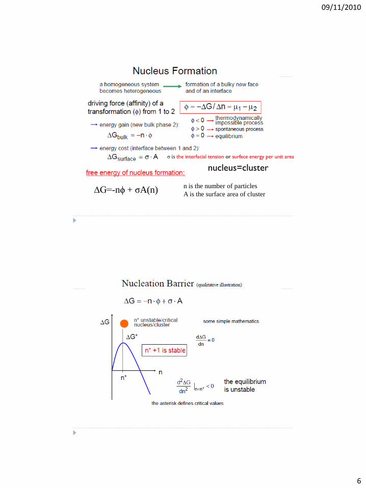
∆G=-nϕ + σA(n)
nucleus=cluster
σ is the interfacial tension or surface energy per unit area
n is the number of particles
A is the surface area of cluster
09/11/2010
7
Classical Nucleation Theory for Cluster
Formation
From experiments,
∆G=-nkBT lnS+4πσ(3υ/4π)2/3n2/3
where σ is the interfacial tension or surface energy per
unit area, A is the surface area of the cluster, ʋ is the
volume per molecule in the bulk liquid, kB is the Boltzmann
constant, T is the temperature, and S, the supersaturation, is
S=P/Pe
P is the vapour pressure and Pe is the equilibrium or 'saturation' vapour pressure
at the temperature of the vapour.
Classical Nucleation Theory for Cluster
Formation
The smallest cluster of size n* which can grow with a decrease in free energy is determined from the condition ∂∆G/∂n = 0. It follows that
∆G(n*)=16πσ3υ2/3(kBT ln S)2
n*=32πσ3ʋ2/3(kBT lnS)3
r*=2σʋ/(kBT lnS)
S, the supersaturation, is P/Pe
ʋ is the volume per molecule in the bulk liquid
P is the vapour pressure and Pe is the equilibrium or 'saturation' vapour pressure
at the temperature of the vapour.
Note
09/11/2010
8
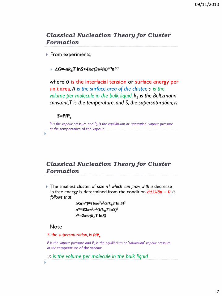
Classical Nucleation Theory for Cluster
Formation
∆G(n*)=16πσ3υ2/3(kBT ln S)2
For S > 1, increasing S reduces the barrier height ∆G(n*)and
the critical size n*, and increases the probability that
fluctuations will allow some clusters to grow large
enough to overcome the barrier and grow into stable
droplets.
Classical Nucleation Theory for Cluster
Formation
Figure 2.1 Free energy of formation as a function of size for several metals for a supersaturation ratio S = 50. Note there is an energy barrier that must be overcome in order to form a stable cluster.
09/11/2010
9
Classical Nucleation Theory for Cluster
Formation
Note that S can be increased either by increasing P or decreasing Pe.
The pressure P can be increased by increasing the rate at which atoms are placed in the vapour or decreasing the rate at which they leave the region where the particle nucleation and growth is occurring.
The pressure Pe can be decreased by decreasing T since Pe is approximately given by
Pe=P0eL(0)/RT
where the latent heat per mole has been approximated by its zero-temperature value L(0), P0 is a constant, and R is the gas constant.
Classical Nucleation Theory for Cluster
Formation
The rate of homogeneous nucleation J, defined as the number of drops nucleated per cubic centimetre per second, is given by
J=K exp[-∆G(n*)/kBT]
The factor K incorporates both the effective collision rate of vapour molecules with a nucleus of size n* and the departure of the cluster distribution from equilibrium.
A critical supersaturation, Sc, can be defined as the supersaturation at which J = 1 cm–3 s–1. Setting J = 1 cm–3 s–1 in equation above, Sc can be obtained using macroscopic values for the surface tension, liquid density, and Pe.
09/11/2010
10
Nanoparticles Produced by Sputtering and
Thermal Evaporation and Laser Methods
The Classical Nucleation Theory discusses the
formation and collection of nanoparticles produced from
a supersaturated vapour produced by thermal
evaporation, sputtering, laser methods, etc.
Scaling Laws
Because of the absence of an exact theory for cluster nucleation and growth, scaling laws are useful for determining the onset conditions for cluster formation.
ζ*=(rch)3-q(Tch)1.5-0.25q
where q (0.5 < q < 1) is a parameter determined experimentally from cluster beam measurements in which the nozzle diameter is varied at constant temperature T0, rch = (m/ρ)1/3, Tch = ΔH0/kB, m is the atomic mass, ρ is the density of the solid, and ΔH0
D is the sublimation enthalpy per atom at 0 K.
09/11/2010
11
Scaling Laws
Empirically it has been found that for: ζ* < 200 no clustering observed
200 < ζ* < 1000 clustering occurs
1000 < ζ* massive condensation occurs with the cluster size > 100 atoms/cluster.
Cluster formation and growth are favoured by decreasing T0and increasing d.
ζ*=(rch)3-q(Tch)1.5-0.25q
Chemical vapor deposition (CVD)
CVD is a chemical process used to produce high-purity,
high-performance solid materials. The process is often
used in the semiconductor industry to produce thin films.
In a typical CVD process, the wafer (substrate) is exposed
to one or more volatile precursors, which react and/or
decompose on the substrate surface to produce the
desired deposit.
Frequently, volatile by-products are also produced, which are removed by gas flow through the reaction chamber.
09/11/2010
12
CVD
In CVD, the vaporized precursors are introduced into a CVD
reactor and adsorb onto a substance held at an elevated
temperature.
These adsorbed molecules will either thermally decompose or
react with other gases/vapours to form crystals.
The CVD process consists of three steps: (a) mass transport
of reactants to the growth surface through a boundary layer
by diffusion, (b) chemical reactions on the growth surface, and
(c) removal of the gas-phase reaction by-products from the
growth surface.
CVD
Nucleation in the gas phase is homogeneous, whereas
nucleation on the substrate is heterogeneous.
Catalysts, usually transition metal particles such as Fe, Ni,
and Co, are also used in the CVD process.
Strained-induced Stranski−Krastanow growth is used to
produce nanoparticles in the CVD process.
09/11/2010
13
CVD
A typical CVD process involving five steps: (1) mass transportation of reactants delivered from the gas/liquid source
to the substrate surface;
(2) the adsorption of reactants on the substrate surface;
(3) the chemical reaction on the substrate surface to form the desired film;
(4) desorption of by-products of the chemical reaction from the substrate surface; and
(5) pumping away of the by-products and unreacted reactant.
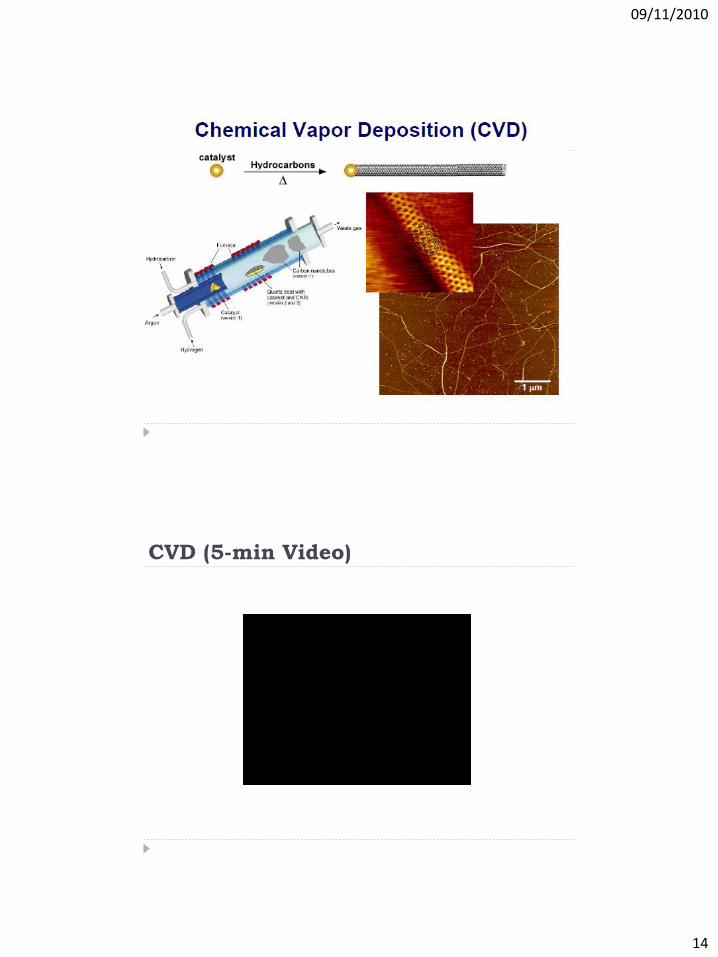
Watching a CNT Growing by CVD (video)
09/11/2010
14
CVD (5-min Video)
09/11/2010
15
Ex. 1 GaN nanotubes were also successfully
produced by CVD.
This reaction was carried out in a conventional furnace with a horizontal quartz tube, where a 4:1 molar mixture of Ga and Ga2O3was placed in an alumina crucible and covered with a porous alumina plate with 3−5 mm diameter channels.
The carbon nanotubes were placed on the porous alumina plate.
The crucible was placed in the hot zone inside the quartz tube and was held in a flowing ammonia atmosphere (400 standard cm3/min) at 1173 K for 1 h.
The Ga2O gas generated from the Ga−Ga2O3 powder mixture flies up toward the region of carbon nanotubes through the porous plate and reacts with the nanotubes and the NH3 gas and produces GaNnanotubes.
GaN nanotubes
09/11/2010
16
TEM images of the starting carbon nanotube
materials and the resulting GaN nanotubes.
(A) Carbon nanotubes used as starting material and (B) GaN nanorods produced
by CVD.
Substances commonly deposited for Integrated Circuits (ICs)
Polysilicon
Polycrystalline silicon is deposited from silane (SiH4), using the
following reaction:
SiH4 → Si + 2 H2 This reaction is usually performed in LPCVD
systems, with either pure silane feedstock, or a solution of
silane with 70-80% nitrogen. Temperatures between 600 and
650 °C and pressures between 25 and 150 Pa yield a growth
rate between 10 and 20 nm per minute.
09/11/2010
17
Types of chemical vapor deposition
A number of forms of CVD are in wide use and are frequently referenced in the literature. These processes differ in the means by which chemical reactions are initiated (e.g., activation process) and process conditions.
Classified by operating pressure Atmospheric pressure CVD (APCVD) - CVD processes at atmospheric
pressure.
Low-pressure CVD (LPCVD) - CVD processes at sub-atmospheric pressures. Reduced pressures tend to reduce unwanted gas-phase reactions and improve film uniformity across the wafer. Most modern CVD processes are either LPCVD or UHVCVD.
Ultrahigh vacuum CVD (UHVCVD) - CVD processes at a very low pressure, typically below 10−6 Pa (~10−8 torr). Note that in other fields, a lower division between high and ultra-high vacuum is common, often 10−7 Pa.
Ex. 2 Silicon dioxide
Silicon dioxide can be deposited by several different
processes. Common source gases include silane and
oxygen, dichlorosilane (SiCl2H2) and nitrous oxide (N2O),
or tetraethylorthosilicate (TEOS; Si(OC2H5)4).
The reactions are as follows:
SiH4 + O2 → SiO2 + 2 H2
SiCl2H2 + 2 N2O → SiO2 + 2 N2 + 2 HCl
Si(OC2H5)4 → SiO2 + byproducts
09/11/2010
18
Ex. 3 Silicon nitride
Silicon nitride is often used as an insulator and chemical
barrier in manufacturing ICs. The following two reactions
deposit nitride from the gas phase:
3 SiH4 + 4 NH3 → Si3N4 + 12 H2 3
SiCl2H2 + 4 NH3 → Si3N4 + 6 HCl + 6 H2
Another two reactions may be used in plasma to deposit
SiNH:
2 SiH4 + N2 → 2 SiNH + 3 H2
SiH4 + NH3 → SiNH + 3 H2
Ex. 4 Metals
CVD processes for molybdenum, tantalum, titanium,
nickel, and tungsten are widely used.
2 MCl5 + 5 H2 → 2 M + 10 HCl
The usual source for tungsten is tungsten hexafluoride,
which may be deposited in two ways:
WF6 →W + 3 F2
WF6 + 3 H2 →W + 6 HF
09/11/2010
19
Physical Vapour Deposition (PVD)
PVD involves condensation from the vapour phase.
The process does not involve a chemical reaction.
The PVD process is composed of three main steps:
(a) generating a vapour phase by evaporation or sublimation of
the material,
(b) transporting the material from the source to the substrate,
and
(c) formation of the particle and/or film by nucleation and
growth.
Physical Vapour Deposition (PVD)
Different techniques have been used to evaporate the
source such as electron beam, thermal energy, sputtering,
cathodic arc plasma, and pulsed laser.
Si nanowire, GeO2 nanowire, Ga2O3 nanowire, ZnO
nanorod, GaO nanobelt and nanosheet, SnO2 nanowire,
nanoribbon, nanotube, etc., have been synthesized using
PVD.
09/11/2010
20
Thermal Evaporation
Thermal evaporation consists of two steps: Material is evaporated from a hot source and then condenses on a relatively cold surface.
The most commonly observed thermal evaporation is the evaporation and condensation of water on the lid of the cooking pot.
In film deposition, thermal evaporation usually takes place in a high vacuum system. Because the energy source is purely thermal energy, the equipment setup is relatively simple.
The deposition species are atoms and ions—usually these atoms and ions do not collide with each other on their journey from the source to the substrate due to high vacuum.
Thermal Evaporation
The advantages of this method are the high deposition
rate and large substrate size.
The downside is that the materials to be deposited are
limited to those with low sublimation or evaporation
temperatures.
09/11/2010
21
Sputtering
Whereas the mechanism for evaporation is thermal
energy, sputtering is based on momentum transfer.
During sputtering, the high-energy ions bombard the
target surface and transfer an amount of kinetic energy
that far exceeds the chemical bonding strength of the
target materials.
Therefore, the source material is ‗‗decomposed‘‘ or
‗‗sputtered‘‘ from the target and deposited on the
substrate.
Schematics of dc sputtering PVD process
09/11/2010
22
PVD animation
Atomic Layer Deposition (ALD)
Definition of ALD
Brief history of ALD
ALD process and equipments
ALD applications
Summary
09/11/2010
23
Definition of ALD
ALD is a method of applying thin films to various substrates with atomic scale precision.
Similar in chemistry to chemical vapor deposition (CVD), except that the ALD reaction breaks the CVD reaction into two half-reactions, keeping the precursor materials separate during the reaction.
ALD film growth is self-limited and based on surface reactions, which makes achieving atomic scale deposition control possible.
By keeping the precursors separate throughout the coating process, atomic layer thickness control of film grown can be obtained as fine as atomic/molecular scale per monolayer.
Brief History of ALD
Introduced in 1974 by Dr. Tuomo Suntola and co-workers
in Finland to improve the quality of ZnS films used in
electroluminescent displays.
Recently, it turned out that ALD also produces outstanding
dielectric layers and attracts semiconductor industries for
making High-K dielectric materials.
09/11/2010
24
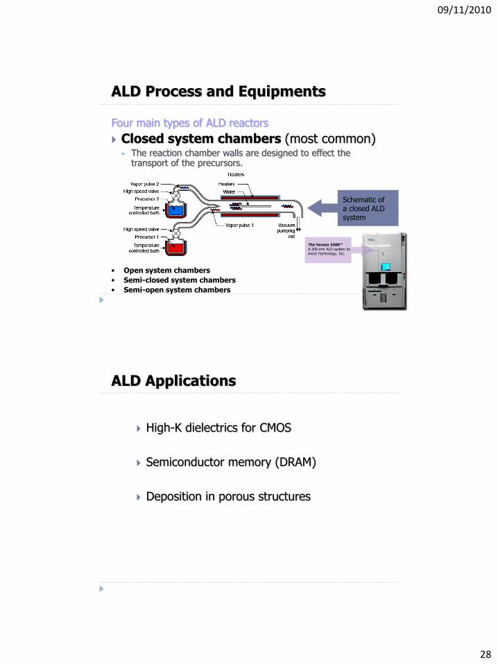
ALD Process and Equipments
Releases sequential precursor gas pulses to deposit a film one layer at a time on the substrate.
The precursor gas is introduced into the process chamber and produces a monolayer of gas on the wafer surface. A second precursor of gas is then introduced into the chamber reacting with the first precursor to produce a monolayer of film on the wafer surface.Two fundamental mechanisms: Chemisorption saturation process Sequential surface chemical reaction process
Example: ALD cycle for Al2O3 deposition
Since each pair of gas pulses (one cycle) produces exactly one monolayer of film, the thickness of the resulting film may be precisely controlled by the number of deposition cycles.
ALD Process and Equipments
• Example: ALD cycle for Al2O3 deposition (Step 1a)
09/11/2010
25
ALD Process and Equipments
• Example: ALD cycle for Al2O3 deposition (Step 1b)
ALD Process and Equipments
4/25/06EE 518 Class Presentation50
• Example: ALD cycle for Al2O3 deposition (Step 1c)
knudson effusion cells (e.g., Ga and As) until they begin
to slowly sublimate.
Gaseous elements then condense on the wafer, where
they may react with each other (e.g., GaAs).
The term ―beam‖ means the evaporated atoms do not
interact with each other or with other vacuum chamber
gases until they reach the wafer.
64
09/11/2010
33
Example: In2O3 on Y-stabilized ZrO2(100) by MBE
65
Top-Down Approach
Milling is a typical top-down method in making nanoparticles.
Etching/lithography
The biggest problem with top-down approach is the imperfection of the surface structure. It is well known that the conventional top-down techniques such as lithography can cause significant crystallographic damage to the processed patterns.
For example, nanowires made by lithography is not smooth and may contain a lot of impurities and structural defects on surface.
09/11/2010
34
Top-Down Approach
Such imperfections would have a significant impact on physical properties and surface chemistry of nanostructures and nanomaterials, since the surface over volume ratio in nanostructures and nanomaterials is very large.
The surface imperfection would result in a reduced conductivity due to inelastic surface scattering, which in turn would lead to the generation of excessive heat and thus impose extra challenges to the device design and fabrication.
Stainless steel –very effective due to their high density
and low contamination of the material being processed,
Stainless steel balls are unsuitable for some applications,
including: Black powder and other flammable materials require
non-sparking lead, antimony, brass, or bronze grinding media
Contamination by iron of sensitive substances such as ceramic
raw materials.
Alumina (90–95% alumina) is widely used in the ceramic
industry to grind clay bodies, frits, glazes and other
ingredients.
Ball Mill
A ball mill is a type of grinder, a cylindrical device , used to
grind materials into extremely fine powder for use in mineral
dressing processes, paints, pyrotechnics, and ceramics.
Ball mills rotate around a horizontal axis, partially filled with
the material to be ground plus the grinding medium. Different
materials are used as media, including ceramic balls and
stainless steel balls.
High-quality ball mills are potentially expensive and can grind
mixture particles to as small as 5 nm, enormously increasing
surface area and reaction rates.
09/11/2010
36
Nanolithography: Top-Down Approach
Nanolithography has been used to advance areas of modern science and technology such as the production of integrated circuits, information storage devices, video screens, microelectromechanical systems (MEMS), miniaturized sensors, microfluidic devices, biochips, photonic bandgap structures, and diffractive optical elements.
Generally, nanolithography can be divided into two categories based on the patterning strategy used: parallel replication and serial writing.
Parallel replication methods such as photolithography, contact printing, and nanoimprint lithography are useful for high throughput, large-area patterning.
Nanolithography: Top-Down Approach
However, most of these methods can only duplicate
patterns, which are predefined by serial writing
approaches and thus cannot be used to arbitrarily
generate different patterns (that is, one photomask leads
to one set of feature sizes for a given wavelength).
In contrast, serial writing methods, such as scanning probe
lithography (SPL) can create patterns with high resolution
and precise registration, but they are limited in
throughput.
09/11/2010
37
Parallel Replication
Schematic of the photolithography fabrication process.
which are the mask reticles in photolithography or the
molds in contact printing and nanoimprint lithography.
Photolithography is the oldest top-down method. It uses
light shining through the masked area on a photoresist
coated substrate (a Si wafer).
The substrate is covered by a photoresist, which is the
key to the photolithography process.
09/11/2010
38
Parallel Replication
The photoresist is an organic-based compound.
The limitation of the photolithography technique is the
dimension of patterns.
The size of pattern that can be produced is up to the
wavelength of the light, which limited to about 37 nm. The
process can be done only on a hard flat surface and in a
provided facility.
Microcontact printing
Schematic illustrating the transfer of alkanethiol molecules from an elastomeric stamp to a substrate.
09/11/2010
39
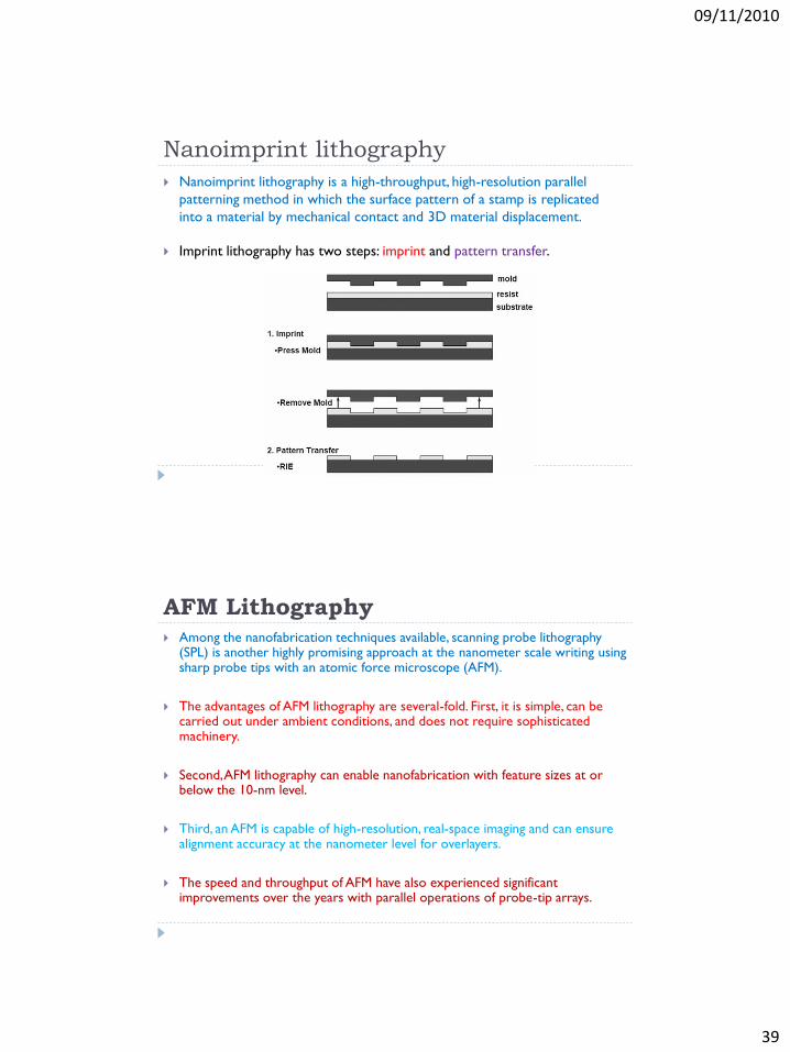
Nanoimprint lithography
Nanoimprint lithography is a high-throughput, high-resolution parallel
patterning method in which the surface pattern of a stamp is replicated
into a material by mechanical contact and 3D material displacement.
Imprint lithography has two steps: imprint and pattern transfer.
AFM Lithography Among the nanofabrication techniques available, scanning probe lithography
(SPL) is another highly promising approach at the nanometer scale writing using sharp probe tips with an atomic force microscope (AFM).
The advantages of AFM lithography are several-fold. First, it is simple, can be carried out under ambient conditions, and does not require sophisticated machinery.
Second, AFM lithography can enable nanofabrication with feature sizes at or below the 10-nm level.
Third, an AFM is capable of high-resolution, real-space imaging and can ensure alignment accuracy at the nanometer level for overlayers.
The speed and throughput of AFM have also experienced significant improvements over the years with parallel operations of probe-tip arrays.
09/11/2010
40
AFM Lithography
Thermomechanical writing by AFM: (a) AFM image of a
sub-100-nm dot array written on polycarbonate using an
electrically heated sharp-cantilever tip with 35-mW, 4-ms
pulses and (b, c) schematics of IBM‘s Millipede.
Bottom-up approach
The colloidal dispersion is a good example of bottom-up approach in the synthesis of nanoparticles.
Bottom-up approach is often emphasized in nanotechnology literature, though bottom-up is nothing new in materials synthesis.
Typical material synthesis is to build atom by atom on a very large scale, and has been in industrial use for over a century.
Bottom-up approach refers to the build-up of a material from the bottom: atom-by-atom, molecule-by-molecule, or cluster-by-cluster.
09/11/2010
41
Bottom-up approach
Bottom-up approach also promises a better chance to
obtain nanostructures with less defects, more
homogeneous chemical composition, and better short
and long range ordering.
This is because the bottom-up approach is driven mainly
by the reduction of Gibbs free energy, so that
nanostructures and nanomaterials such produced are in a
state closer to a thermodynamic equilibrium state.
Sol-gel Process
Sol-gel consists of two words (sol and gel). A sol is defined as a dispersion of solid particles having the size below 1 µm in a liquid media (i.e., water, acetone, acetonitrile, and ethanol) where the Brownian motions suspend the colloidal particles while a gel is a state where both liquid and solid are dispersed in each other, leading to a solid network, which contains liquid components.
The sol-gel process is a facile wet-chemical technique, which is typically used in the field of nanomaterials.
It can be used for producing nanocolloids of metals, and metal oxides.
09/11/2010
42
Nanoscale dispersion (video)
(Real-time Video of nanoparticles suspended in water)
Nanoparticles produced using Sol-gel process
09/11/2010
43
09/11/2010
44
Milestones of Sol-gel Process
Back to the mid-1800s, Ebelman and Graham made silica gel
(SiO2) by using the simple hydrolysis reaction of tetraethyl
orthosilicate (TEOS), Si(OC2H5)4, under the mild acidic
reaction.
Afterwards, this reaction became known as the first reaction
of sol-gel process.
In the 1950s and 1960s, Roy employed the sol-gel process in
producing the highly homogeneous colloidal gels of ceramic
oxides, which involved Al, Si, Ti, Zr, etc., that could not be made
by using the conventional ceramic powder methods.
Milestones of Sol-gel Process
In the meantime, the colloidal silica powder named Du Pont‘s colloidal Ludox spheres was marketed for the first time from the Iler‘s pioneering work in the silica chemistry.
Stober et al. (1992) had in addition done more challenging work using the sol-gel process in controlling the morphology and size of colloids yielding the so-called Stober spherical silica powder.
Unquestionably, this finding has led to current frontier research in the field of nanoscience and nanotechnology known as the bottom-up approach for which nanomaterials are produced from chemical monomer precursors.
09/11/2010
45
Sol-gel Deposition
There are four steps in general for the sol-gel coating process as follows:
(i) the desired colloidal nanomaterials are firstly dispersed in a liquid media to form a sol.
(ii) the deposition of the sol suspension produces coatings on the substrates by spraying, dipping, dropping or spinning.
(iii) the particles in the sol are polymerized through the removal of the stabilizing components and produce a gel in a state of a continuous network.
(iv) the final heat treatments pyrolyze the remaining organic or inorganic components and form an amorphous or crystalline nanomaterials on the desired substrates.
Sol-gel Technology
Owing to the simplicity and low cost of the sol-gel process,
sol-gel technology has significantly impacted on the fields of
engineering ceramics and glass.
There are many current companies all around the world based
on the sol-gel technology such as Advanced Industrial
Materials (Canada), Aspen Systems, Inc. (USA), Gaematech. Co.,
Ltd. (Switzerland), Sol-Gel Technologies (Israel), and Sustainable
Technologies Australia Ltd (Australia).
09/11/2010
46
Sol—Gel Processing of Silica
The sol-gel process for preparing silica and silicates from metal alkoxide
precursors is reviewed and compared to the processing of aqueous
silicates as described by Iler.
Sol-gel processing combines control of composition and microstructure at
the molecular level with the ability to shape material in bulk, powder, fiber,
and thin-film form.
In sol-gel processing of metal alkoxides, hydrolysis reactions replace an
alkoxide group with a hydroxyl group.
Subsequent condensation reactions involving the hydroxyl groups produce
siloxane bonds.
Sol—Gel Processing of Silica
The structure of the evolving silicates is a consequence of the successive
polymerization, gelation, aging, drying, and heating steps.
Often the structures of polymers, gels, and dried gels (either xerogels or
aerogels) may be characterized on the 1-20-nm length scale by a mass or
surface fractal dimension.
On longer length scales, dried gels are micro- or mesoporous, with surface
areas often exceeding 800 m2/g.
During heating, these gels undergo continued polymerization, structural
relaxation, and viscous sintering; dense amorphous silica essentially
indistinguishable from its conventionally prepared counterpart ultimately results.
09/11/2010
47
Sol-gel process
•Aerogel is derived from a
gel in which the liquid
component of the gel has
been replaced with a gas.
•The result is an
extremely low-density
solid, with a notable
effectiveness as a thermal
insulator.
A xerogel is a solid formed from a gel by
drying with unhindered shrinkage.
It usually retains high porosity and enormous
surface area along with very small pore size
(1-10 nm).
A sol is a colloidal suspension of solid particles
in a continuous liquid medium.
Sol-gel Process
09/11/2010
48
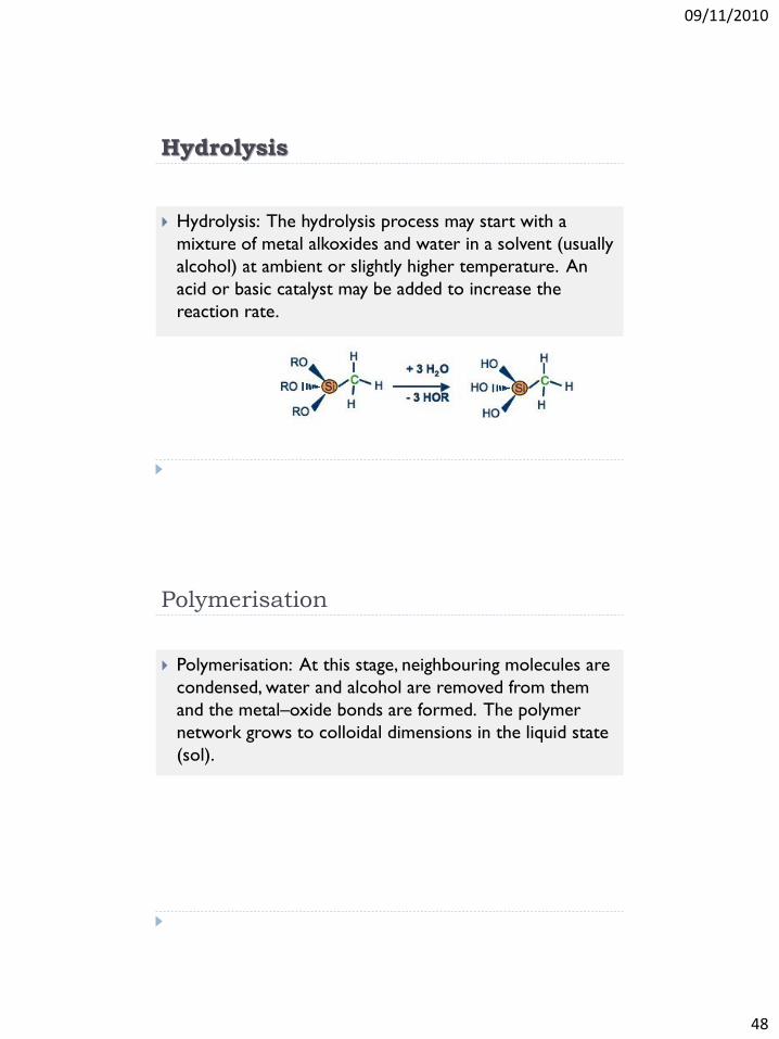
Hydrolysis
Hydrolysis: The hydrolysis process may start with a
mixture of metal alkoxides and water in a solvent (usually
alcohol) at ambient or slightly higher temperature. An
acid or basic catalyst may be added to increase the
reaction rate.
Polymerisation
Polymerisation: At this stage, neighbouring molecules are
condensed, water and alcohol are removed from them
and the metal–oxide bonds are formed. The polymer
network grows to colloidal dimensions in the liquid state
(sol).
09/11/2010
49
Gelification
Gelification: In this stage, the polymer network keeps
growing until a three dimensional network is formed
through the ligand. The system becomes slightly stiff,
which is a typical feature of a gel upon removal of the sol
solvent. The solvent, water and alcohol molecules remain,
however, inside the gel pores. The addition of smaller
polymer units to the main network continues
progressively with gel ageing.
Drying
Drying: Water and alcohol are removed at mild
temperatures (<470 K), giving rise to hydroxylated metal
oxides with a residual organic content. If the aim is to
prepare an aerogel with high specific surface and low
density, the solvent must be removed under supercritical
conditions.
09/11/2010
50
Dehydration
Dehydration: This stage is performed between 670 and
1070K to remove the organic residue and chemically
bonded water. The result is a metal oxide in glass or
microcrystalline form, with microporosity higher than 20–
30%.
Densification
Densification: At temperatures above 1270K we can
obtain dense materials, due to the reaction between the
various components of the precursor in the previous
stage.
09/11/2010
51
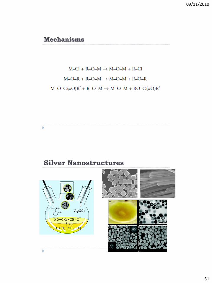
Mechanisms
Silver Nanostructures
09/11/2010
52
Electrochemical deposition
Electrochemical deposition is a low-cost and simple technique, which is well known as an effective method for producing coatings of metals and alloys by reducing metal ions from aqueous electrolytes with an external applied potential or current.
It is used for example to improve corrosion resistance or specific physical and mechanical properties.
Traditional applications have been in the aerospace, automotive, oil and gas, and chemical processing industries.
Electrochemical deposition
An interesting early paper found in the literature by
Cavallaro and Bolognesi was concerned with the
electrochemical deposition of Zn crystals.
More interestingly, not only metals, but also metal oxides
including semiconductors and insulators can be produced
by this technique.
This is very applicable to the field of nanotechnology,
which is often involved with advanced semiconductor
materials.
09/11/2010
53
Electrochemical deposition
Electrochemical deposition
The electrochemical deposition is based on an
electrochemical reaction forming a solid phase from liquid
phase or even sometimes from gas phase (e.g., O2
bubbling gas).
solidM
electrodezeM solution
Z
09/11/2010
54
Electrochemical Deposition
WERECE
v
M+ A- M+
e-WERE
CE
A-
The principle “when solutions containing H2O, H2O2, NO3- or O2 are subject to
electrolysis at negative potentials, reduction to OH- occurs raising the local pH at the electrode surface. Precipitation of hydroxide, followed by dehydration occurs to form oxide films.”
Topics are related to ‗Syntheses of Nanomaterials‘
Template of the report
Synthesis of ........
Methodology Processes and Principles......
Results: SEM, TEM, AFM (images)
References
Sources: ISI web of science and Scopus
09/11/2010
57
References Nanomaterials and Nanochemistry by C. Brechignac, P. Houdy, and M.
Lahmani, Springer (2006)
Nanoscale Devices by G.F. Cerofolini, Springer (2009) Chapters 1-3 and 9-12
Nanocomposite Science and Technology by P.M. Ajayan, L.S. Schadler, and P.V. Braun (2003) Chapters 1-3
Handbook of Nanoscience, Engneering, and Technology (second edition)by W. A. Goddard III, D. W. Brenner, S. E. Lyshevski, and G.J. Iafrate, CRC Press (2007) Chapter 1
Carbon Nanotubes Properties and Applications by M. J. O’Connell, CRC Press (2006) Chapters1, 4, 7, and 9
Nanotechnology: An Introduction to Nanostructuring Techniques by M. Kohler and W Fritzsche, WILEY-VCH (2004) Chapter 1