Tandem, triple and quadruple junction polymer solar cells Citation for published version (APA): Di Carlo Rasi, D. (2018). Tandem, triple and quadruple junction polymer solar cells. Eindhoven: Technische Universiteit Eindhoven. Document status and date: Published: 10/12/2018 Document Version: Publisher’s PDF, also known as Version of Record (includes final page, issue and volume numbers) Please check the document version of this publication: • A submitted manuscript is the version of the article upon submission and before peer-review. There can be important differences between the submitted version and the official published version of record. People interested in the research are advised to contact the author for the final version of the publication, or visit the DOI to the publisher's website. • The final author version and the galley proof are versions of the publication after peer review. • The final published version features the final layout of the paper including the volume, issue and page numbers. Link to publication General rights Copyright and moral rights for the publications made accessible in the public portal are retained by the authors and/or other copyright owners and it is a condition of accessing publications that users recognise and abide by the legal requirements associated with these rights. • Users may download and print one copy of any publication from the public portal for the purpose of private study or research. • You may not further distribute the material or use it for any profit-making activity or commercial gain • You may freely distribute the URL identifying the publication in the public portal. If the publication is distributed under the terms of Article 25fa of the Dutch Copyright Act, indicated by the “Taverne” license above, please follow below link for the End User Agreement: www.tue.nl/taverne Take down policy If you believe that this document breaches copyright please contact us at: [email protected]providing details and we will investigate your claim. Download date: 29. May. 2020
Transcript
Tandem, triple and quadruple junction polymer solar cells
Citation for published version (APA):Di Carlo Rasi, D. (2018). Tandem, triple and quadruple junction polymer solar cells. Eindhoven: TechnischeUniversiteit Eindhoven.
Document status and date:Published: 10/12/2018
Document Version:Publisher’s PDF, also known as Version of Record (includes final page, issue and volume numbers)
Please check the document version of this publication:
• A submitted manuscript is the version of the article upon submission and before peer-review. There can beimportant differences between the submitted version and the official published version of record. Peopleinterested in the research are advised to contact the author for the final version of the publication, or visit theDOI to the publisher's website.• The final author version and the galley proof are versions of the publication after peer review.• The final published version features the final layout of the paper including the volume, issue and pagenumbers.Link to publication
General rightsCopyright and moral rights for the publications made accessible in the public portal are retained by the authors and/or other copyright ownersand it is a condition of accessing publications that users recognise and abide by the legal requirements associated with these rights.
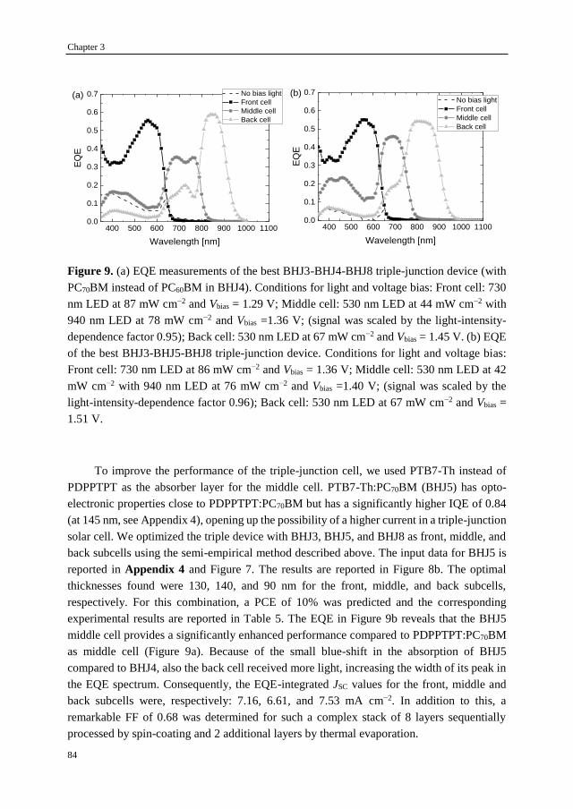
• Users may download and print one copy of any publication from the public portal for the purpose of private study or research. • You may not further distribute the material or use it for any profit-making activity or commercial gain • You may freely distribute the URL identifying the publication in the public portal.
If the publication is distributed under the terms of Article 25fa of the Dutch Copyright Act, indicated by the “Taverne” license above, pleasefollow below link for the End User Agreement:www.tue.nl/taverne
Take down policyIf you believe that this document breaches copyright please contact us at:[email protected] details and we will investigate your claim.
(CIGS) and the relatively new lead halide perovskites. Efficiencies of in order, 14.0%, 28.8%,
22.1%, 22.6% and 22.1% have now been reached by these thin-film technologies.[9] While
these materials present an advantage in terms of absorption coefficient over crystalline
silicon, other aspects such as high cost, use of scarce or toxic elements, and early-stage
technology development currently limit their ubiquitous use. Third generation PV devices
aim at providing very high efficiency at low cost.[10] In this spectrum of PV technologies,
organic photovoltaic (OPV) is now positioned as a second-generation technology that may
provide efficiencies similar to other thin-film technologies, but allows easy processing from
solution, use of non-toxic organic semiconductors, flexibility of panels, and the possibility to
adjust color and transparency. As such OPV offers opportunities e.g. in building integrated
panels that cannot be met by other PV technologies at present.
Introduction
3
1.2 Organic solar cells
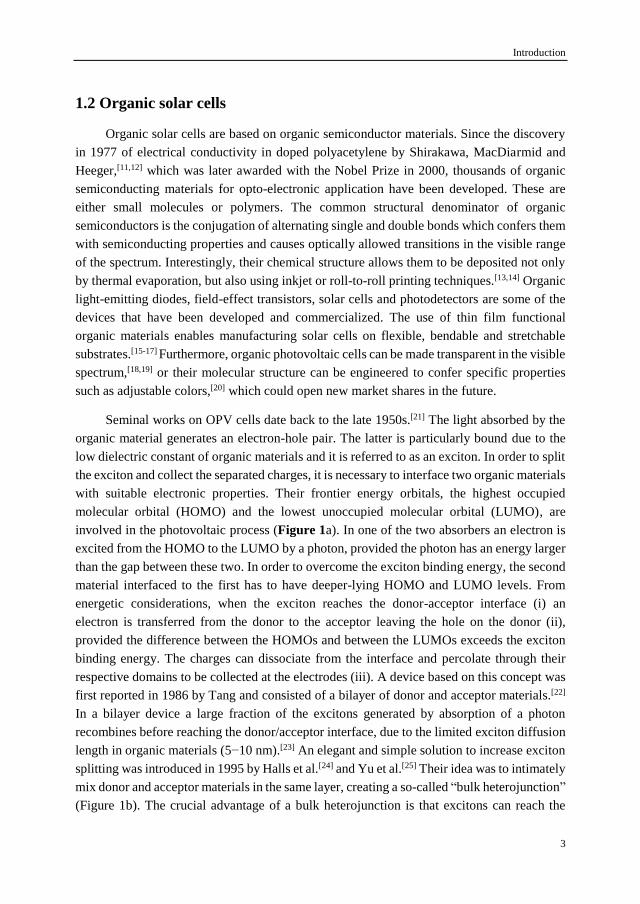
Organic solar cells are based on organic semiconductor materials. Since the discovery
in 1977 of electrical conductivity in doped polyacetylene by Shirakawa, MacDiarmid and
Heeger,[11,12] which was later awarded with the Nobel Prize in 2000, thousands of organic
semiconducting materials for opto-electronic application have been developed. These are
either small molecules or polymers. The common structural denominator of organic
semiconductors is the conjugation of alternating single and double bonds which confers them
with semiconducting properties and causes optically allowed transitions in the visible range
of the spectrum. Interestingly, their chemical structure allows them to be deposited not only
by thermal evaporation, but also using inkjet or roll-to-roll printing techniques.[13,14] Organic
light-emitting diodes, field-effect transistors, solar cells and photodetectors are some of the
devices that have been developed and commercialized. The use of thin film functional
organic materials enables manufacturing solar cells on flexible, bendable and stretchable
substrates.[15-17] Furthermore, organic photovoltaic cells can be made transparent in the visible
spectrum,[18,19] or their molecular structure can be engineered to confer specific properties
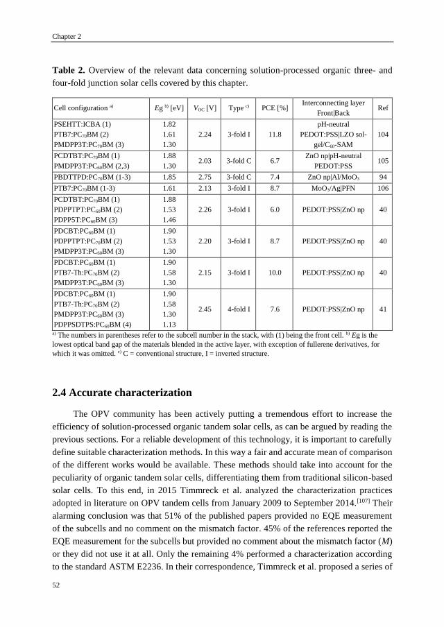
such as adjustable colors,[20] which could open new market shares in the future.
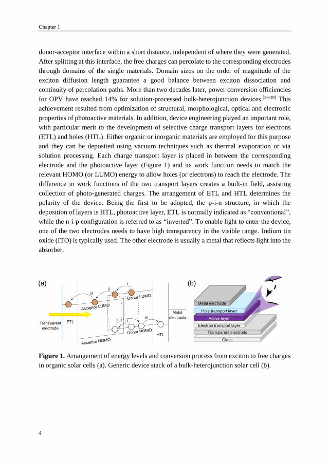
Seminal works on OPV cells date back to the late 1950s.[21] The light absorbed by the
organic material generates an electron-hole pair. The latter is particularly bound due to the
low dielectric constant of organic materials and it is referred to as an exciton. In order to split
the exciton and collect the separated charges, it is necessary to interface two organic materials
with suitable electronic properties. Their frontier energy orbitals, the highest occupied
molecular orbital (HOMO) and the lowest unoccupied molecular orbital (LUMO), are
involved in the photovoltaic process (Figure 1a). In one of the two absorbers an electron is
excited from the HOMO to the LUMO by a photon, provided the photon has an energy larger
than the gap between these two. In order to overcome the exciton binding energy, the second
material interfaced to the first has to have deeper-lying HOMO and LUMO levels. From
energetic considerations, when the exciton reaches the donor-acceptor interface (i) an
electron is transferred from the donor to the acceptor leaving the hole on the donor (ii),
provided the difference between the HOMOs and between the LUMOs exceeds the exciton
binding energy. The charges can dissociate from the interface and percolate through their
respective domains to be collected at the electrodes (iii). A device based on this concept was
first reported in 1986 by Tang and consisted of a bilayer of donor and acceptor materials.[22]
In a bilayer device a large fraction of the excitons generated by absorption of a photon
recombines before reaching the donor/acceptor interface, due to the limited exciton diffusion
length in organic materials (5−10 nm).[23] An elegant and simple solution to increase exciton
splitting was introduced in 1995 by Halls et al.[24] and Yu et al.[25] Their idea was to intimately
mix donor and acceptor materials in the same layer, creating a so-called “bulk heterojunction”
(Figure 1b). The crucial advantage of a bulk heterojunction is that excitons can reach the
Chapter 1
4
donor-acceptor interface within a short distance, independent of where they were generated.
After splitting at this interface, the free charges can percolate to the corresponding electrodes
through domains of the single materials. Domain sizes on the order of magnitude of the
exciton diffusion length guarantee a good balance between exciton dissociation and
continuity of percolation paths. More than two decades later, power conversion efficiencies
for OPV have reached 14% for solution-processed bulk-heterojunction devices.[26-28] This
achievement resulted from optimization of structural, morphological, optical and electronic
properties of photoactive materials. In addition, device engineering played an important role,
with particular merit to the development of selective charge transport layers for electrons
(ETL) and holes (HTL). Either organic or inorganic materials are employed for this purpose
and they can be deposited using vacuum techniques such as thermal evaporation or via
solution processing. Each charge transport layer is placed in between the corresponding
electrode and the photoactive layer (Figure 1) and its work function needs to match the
relevant HOMO (or LUMO) energy to allow holes (or electrons) to reach the electrode. The
difference in work functions of the two transport layers creates a built-in field, assisting
collection of photo-generated charges. The arrangement of ETL and HTL determines the
polarity of the device. Being the first to be adopted, the p-i-n structure, in which the
deposition of layers is HTL, photoactive layer, ETL is normally indicated as “conventional”,
while the n-i-p configuration is referred to as “inverted”. To enable light to enter the device,
one of the two electrodes needs to have high transparency in the visible range. Indium tin
oxide (ITO) is typically used. The other electrode is usually a metal that reflects light into the
absorber.
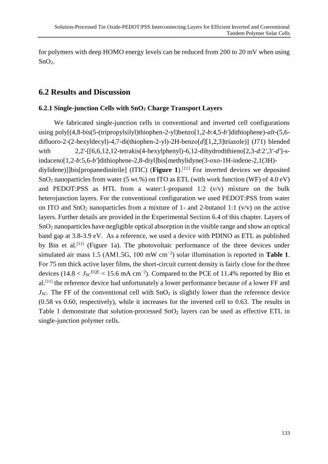
Figure 1. Arrangement of energy levels and conversion process from exciton to free charges
in organic solar cells (a). Generic device stack of a bulk-heterojunction solar cell (b).
Glass
Transparent electrode
Electron transport layer
Active layer
Hole transport layer
Metal electrode
(b) (a)
Introduction
5
1.3 Characterization of solar cells
The standard characterization of solar cells consists in the measurement of their current
density as a function of an applied voltage in sunlight. This returns the J−V characteristic and
it is performed while illuminating the cell under a reference solar spectrum, keeping the cell
at 25 °C. The reference spectrum is the one of the solar light at the sea level and at a latitude
such that the mass of air in the atmosphere through which the light travels is 1.5 times the
one at zenith. This is formally referred to as the AM1.5G spectrum and its intensity is defined
as 100 mW cm−2.[29] Figure 2 shows the tabulated AM1.5G spectrum and an example of a
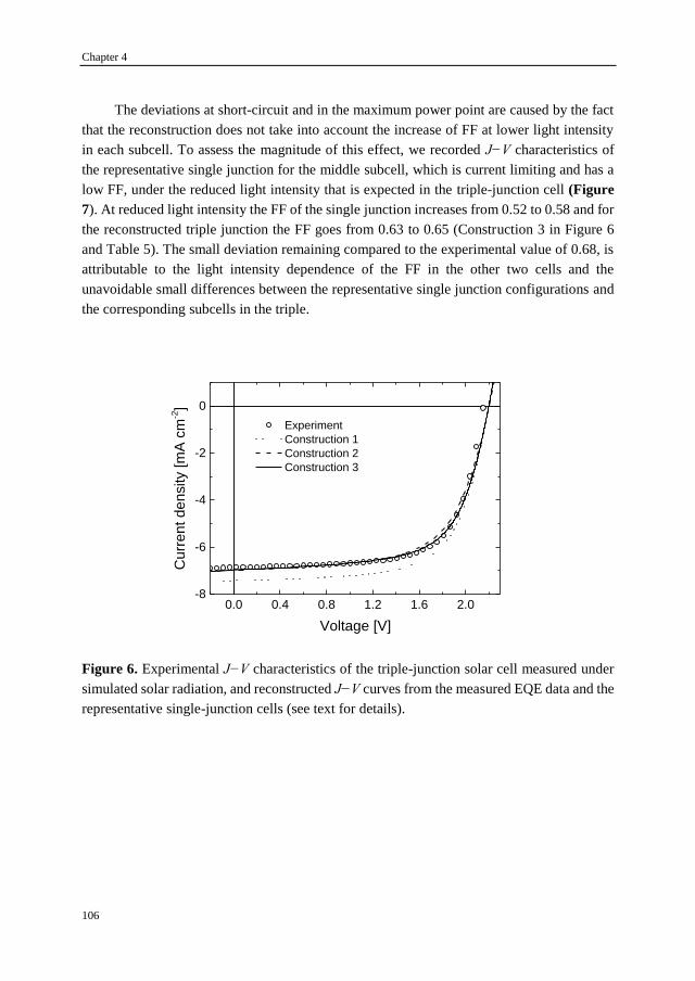
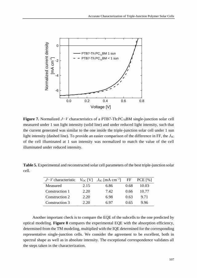
J−V characteristic showing the relevant photovoltaic parameters.
400 600 800 1000 1200 14000.00
0.04
0.08
0.12
0.16
Pow
er
de
nsity [m
W c
m-2 n
m-1]
Wavelength [nm]
100 mW cm-2
(a)
-0.4 0.0 0.4 0.8 1.2 1.6-12
-8
-4
0
JSC
Jmax
Vmax
Curr
en
t d
en
sity [
mA
cm
-2]
Voltage [V]
(b)V
OC
Figure 2. Reference AM1.5G solar spectrum (a), and an example of J−V characteristic of a
solar cell (b).
The relevant information for solar cells that can be derived from the J−V characteristic
lies in the fourth quadrant. The maximum power density the device generates, Pmax,
corresponds to the point on the J−V curve where the product of J and V maximizes. The
voltage and current density at this maximum power point are referred to as Vmax and Jmax,
respectively. Other relevant metrics are the open-circuit voltage VOC and the short-circuit
current density JSC. For organic solar cells the VOC is related to the difference between the
HOMO energy of the donor material and the LUMO energy of the acceptor material. The JSC
is related to the optical band gap of the photoactive layer and the quantum efficiency by
which charges are created and collected. Another relevant parameter is the fill factor (FF).
The FF reflects recombination mechanisms occurring in the device, which affect the
efficiency of charge collection. Referring to Figure 2b, the FF corresponds to the ratio
between the area of the rectangle at maximum power condition and the area of the rectangle
Chapter 1
6
determined by VOC and JSC. In other words, FF = Pmax/(VOC∙JSC). The power conversion
efficiency (PCE) is calculated as Pmax/Pin, where Pin is the power density of the incident light.
Hence, the PCE can be expressed as: PCE = VOC⋅JSC⋅FF/Pin. Because the intensity of the
AM1.5G solar spectrum is 100 mW cm−2, Pmax (expressed in mW cm−2) corresponds
numerically to the PCE (expressed in %). Optimizing the PCE of a solar cell involves the
simultaneous increase of JSC, VOC and FF.
Another useful characteristic of a solar cell is the external quantum efficiency (EQE)
spectrum. The EQE spectrum is measured at each wavelength by comparing the number of
photons Nph(λ) incident on the device to the number of electrons Ne(λ) that can be extracted
under these conditions, usually at short-circuit. The EQE at wavelength λ is defined as the
ratio EQE(λ) = Ne(λ)/Nph(λ). Since a solar simulator cannot reproduce the AM1.5G spectrum
exactly, it is challenging to determine the PCE of a solar cell. Especially, the JSC is very
susceptible to small deviations from the AM1.5G spectrum. The correct JSC can be
determined from measuring the EQE spectrum at short-circuit conditions followed by
numerical of the product of the EQE with the tabulated AM1.5G solar power density
spectrum (Psun). This returns the desired current density (JSCEQE):
JSCEQE = ∫ EQE(λ)⋅Psun(λ)
e λ
h cdλ .
Other quantities appearing in the equation are the elementary charge (e), the Planck constant
(h) and the speed of light (c).
In some cases, the internal quantum efficiency (IQE) spectrum of the photoactive layer
is of interest. The IQE(λ) is the ratio between the number of charges collected (Ne(λ)) and the
number of photons absorbed by the photoactive layer (N′ph(λ)) at each wavelength λ. A
practical way to estimate the IQE derives from a simple manipulation of this definition:
IQE(λ) = Ne(λ)
𝑁′ph(λ) =
EQE(λ)
fA
(λ) ,
where fA(λ) is the fraction of absorbed photons by the photoactive layer (fA = N′ph(λ)/Nph(λ)).
fA is a quantity that can be estimated via optical modeling simulations. Interference effects
play an important role in determining the fraction of photons absorbed by the photoactive
layer in an OPV stack of semitransparent thin films because the total thickness is on the same
order of magnitude as the wavelength of visible light. As reported in the experimental section
of some chapters of this thesis, it is sometimes useful to use the spectrally integrated average
IQE. This quantity can be determined from IQE = JSCEQE/JSC
max, where JSCmax is obtained
from integration of fA with the AM1.5G reference spectrum. When using the spectrally
integrated IQE one effectively assumes that the IQE is independent of the wavelength over
the wavelength range where the photoactive layer absorbs light.
Introduction
7
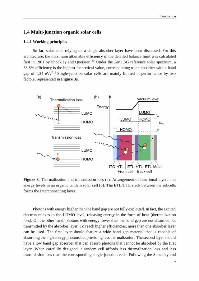
1.4 Multi-junction organic solar cells
1.4.1 Working principles
So far, solar cells relying on a single absorber layer have been discussed. For this
architecture, the maximum attainable efficiency in the detailed balance limit was calculated
first in 1961 by Shockley and Queisser.[30] Under the AM1.5G reference solar spectrum, a
33.8% efficiency is the highest theoretical value, corresponding to an absorber with a band
gap of 1.34 eV.[31] Single-junction solar cells are mainly limited in performance by two
factors, represented in Figure 3a.
Figure 3. Thermalization and transmission loss (a). Arrangement of functional layers and
energy levels in an organic tandem solar cell (b). The ETL/HTL stack between the subcells
forms the interconnecting layer.
Photons with energy higher than the band gap are not fully exploited. In fact, the excited
electron relaxes to the LUMO level, releasing energy in the form of heat (thermalization
loss). On the other hand, photons with energy lower than the band gap are not absorbed but
transmitted by the absorber layer. To reach higher efficiencies, more than one absorber layer
can be used. The first layer should feature a wide band gap material that is capable of
absorbing the high energy photons but providing less thermalization. The second layer should
have a low band gap absorber that can absorb photons that cannot be absorbed by the first
layer. When carefully designed, a tandem cell affords less thermalization loss and less
transmission loss than the corresponding single-junction cells. Following the Shockley and
Chapter 1
8
Queisser detailed balance limit a double-junction (tandem) cell can reach a maximum
efficiency of 42% and a triple-junction cell 49%.[32]
To make a tandem cell the two complementary absorber layers must be connected both
optically and electrically in the same device. A series connection can be accomplished using
an interconnecting layer (ICL), made of a stack of similar interlayer materials used in single-
junction cells. Figure 3b provides a schematic representation of an organic tandem solar cell.
The role of the ICL is to provide an internal contact for recombination of charges from the
active layers, as suggested by the arrows. This internal recombination is necessary to sustain
the photocurrent in the tandem cell. A simple schematic representation of the energy levels
in an OPV tandem is given in Figure 3b. As for single-junction cells, the HTL and the ETL
Fermi level needs to match the relevant HOMO and LUMO levels. These materials also need
to have sufficient Ohmic character to guarantee fast recombination of charges and avoid
voltage loss in the ICL. The voltage of the tandem is the sum of the voltages of the subcells,
since these are connected in series. Therefore the VOC is ideally the sum of the VOCs of the
subcells. Also for tandem cells, the arrangement of HTLs and ETLs determines the polarity
of the device. Because the subcells are connected in series, the photocurrent of a tandem solar
cell is limited by the subcell generating less current. Thus to overcome the intrinsic limits of
single-junction cells, it is of paramount importance that the subcells of a series-connected
tandem cell absorb in complementary regions of the solar spectrum and generate equal
photocurrent.
1.4.2 Early developments
In the first demonstrations of tandem organic solar cells, the materials were thermally
evaporated. Initially only metal clusters were used to interconnect the subcells,[33-35] later
complemented by p- and n-doped organic transport layers.[36,37] In a second stage, active
layers based on solution-processed materials were introduced, with the aim of further moving
the manufacturing towards all-solution-processing.[38,39] The latter consisted of an electron-
donating polymer and an electron-accepting fullerene derivative. In these first publications,
only one active layer was processed from solution and the other one by thermal evaporation.
This choice derived from the intricate requirements of processing all the layers from solution
on top of each other. Further advances in the research field allowed to interconnect in the
same device two solution-processed active layers, first by connecting two single-junction
solar cells deposited on individual substrates,[40] and then by integrating the two subcells
monolithically on the same substrate.[41] In 2007 the first all-solution-processed tandem
polymer solar cells were reported by Gilot et al.[42] and Heeger et al.[43] In both cases the ICL
featured a layer of poly(3,4-ethylenedioxythiophene):polystyrene sulfonate (PEDOT:PSS) as
HTL, stacked on top of a metal oxide layer as ETL. In one case,[42] the stack consisted of zinc
oxide nanoparticles on top of which a pH-neutral formulation of PEDOT:PSS was casted. In
the other case,[43] a film of titanium oxide obtained via a sol-gel route was followed by
Introduction
9
deposition of PEDOT:PSS. The tandem in this second work yielded a PCE of 6.5%.
PEDOT:PSS was later adopted in the vast majority of the tandem solar cells reported (see
also Chapter 2). Starting from there, several advances have been accomplished, which
contributed to increase the efficiency. These improvements concerned for instance the use of
photoactive blends that could afford a high VOC, relative to their optical band gap Eg.[44] This
is usually expressed as the minimum photon energy-loss (Eloss), defined as Eloss = Eg – eVOC.
It must be noted though that the real energy loss per converted photon under operating
condition is higher than Eloss, and it corresponds to E – eVmax, E being the photon’s energy.
As stressed in the previous paragraph, it is important to have active layers with
complementary absorption spectra. The development of low band gap absorbers with
increased performance paved the way towards tandems with efficiencies of 8.6% in 2012[45],
and 10.6% in 2013[46], at hand of Yang and coworkers. On the manufacturing perspective, as
alternative to the initially developed conventional structure, inverted tandem solar cells made
their advent.[47] The ICL was also object of developments, gaining properties like enhanced
resistance against common solvents like chlorobenzene, used for the processing of the back
cell.[48] Self-assembled layers were introduced to engineer the work function at the ICL, and
match the active layer’s relevant frontier energy levels. One of these was the partially
ethoxylated polyethylenimine (PEIE), used to lower the work function of PEDOT:PSS and
match the back cell’s acceptor LUMO.[49] In 2013, Heeger and coworkers found that a similar
function could be carried out by a conjugated polyelectrolyte.[50] As will be discussed in
Chapter 2, this innovation permitted polymer:fullerene based tandem solar cells to set their
record efficiency above 11% in 2015.
Multi-junction cells based on more than two absorber layers have been demonstrated
as well. Initial studies demonstrated the feasibility of realizing such intricate device
structures, both by thermal evaporation[34] as well as via solution-processing[42,51] and with
up to 10[52] and 6 active layers[53], respectively. Triple-junction devices in particular moved
progressively forward with the efficiency, reaching an outstanding 13.2% for evaporated
cells.[54] For solution-processed triples, a PCE of 5.3% was reported in 2013 by Esiner et
al.[55] and 9.6% by Li et al. the same year.[56] Both these triples featured a wide band gap
absorber in the front cell and the same small band gap absorber as both middle and back
subcells. The choice of using twice the same absorber, although not ideal, was practically
successful in virtue of the high current generated by the low band gap cell, with respect to
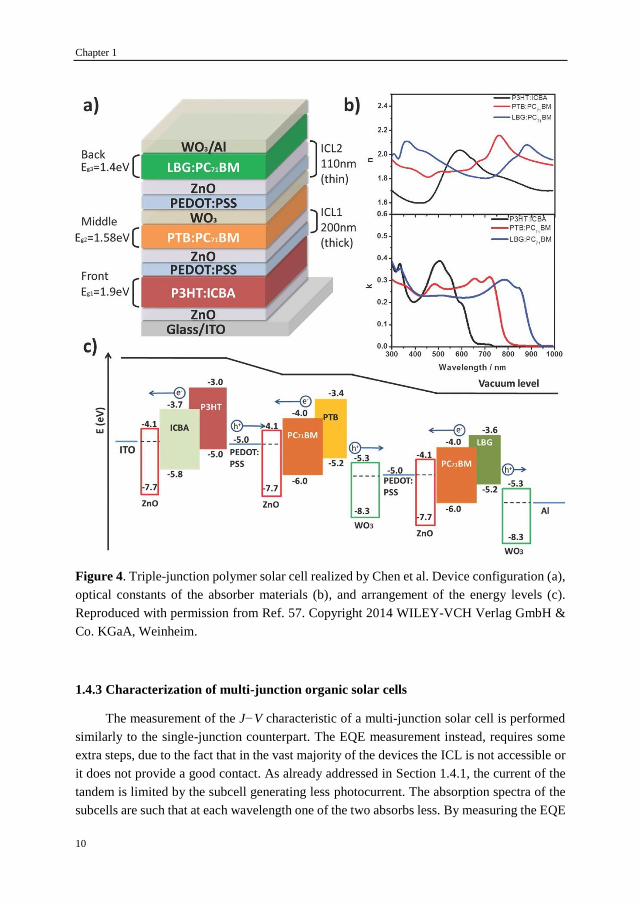
the wide band gap front cell. A remarkable efficiency of 11.6% was reported in 2014 by Yang
and coworkers for a triple-junction cell where active layers with complementary band gaps
were adopted.[57] Figure 4 shows the device stack and optical properties of the three active
layers of this device. The complementarity of the absorption spectra and optimization of
interference effects afforded a high JSC of 7.6 mA cm−2. In addition, a VOC of 2.28 V and FF
of 0.66 contributed to the high efficiency.
Chapter 1
10
Figure 4. Triple-junction polymer solar cell realized by Chen et al. Device configuration (a),
optical constants of the absorber materials (b), and arrangement of the energy levels (c).
Reproduced with permission from Ref. 57. Copyright 2014 WILEY-VCH Verlag GmbH &
Co. KGaA, Weinheim.
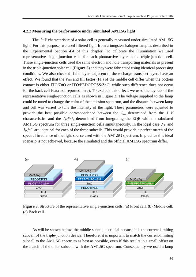
1.4.3 Characterization of multi-junction organic solar cells
The measurement of the J−V characteristic of a multi-junction solar cell is performed
similarly to the single-junction counterpart. The EQE measurement instead, requires some
extra steps, due to the fact that in the vast majority of the devices the ICL is not accessible or
it does not provide a good contact. As already addressed in Section 1.4.1, the current of the
tandem is limited by the subcell generating less photocurrent. The absorption spectra of the
subcells are such that at each wavelength one of the two absorbs less. By measuring the EQE
Introduction
11
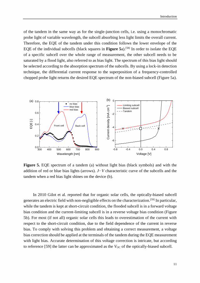
of the tandem in the same way as for the single-junction cells, i.e. using a monochromatic
probe light of variable wavelength, the subcell absorbing less light limits the overall current.
Therefore, the EQE of the tandem under this condition follows the lower envelope of the
EQE of the individual subcells (black squares in Figure 5a).[58] In order to isolate the EQE
of a specific subcell over the whole range of measurement, the other subcell needs to be
saturated by a flood light, also referred to as bias light. The spectrum of this bias light should
be selected according to the absorption spectrum of the subcells. By using a lock-in detection
technique, the differential current response to the superposition of a frequency-controlled
chopped probe light returns the desired EQE spectrum of the non-biased subcell (Figure 5a).
300 400 500 600 700 800 9000.0
0.2
0.4
0.6
0.8
EQ
E [-]
Wavelength [nm]
no bias
blue bias
red bias
Front cell Back cell
(a)
-0.8 -0.4 0.0 0.4 0.8
-6
-4
-2
0
Cu
rre
nt
den
sity [
mA
cm
-2]
Voltage [V]
Limiting subcell
Biased subcell
Tandem
(b)
Figure 5. EQE spectrum of a tandem (a) without light bias (black symbols) and with the
addition of red or blue bias lights (arrows). J−V characteristic curve of the subcells and the
tandem when a red bias light shines on the device (b).
In 2010 Gilot et al. reported that for organic solar cells, the optically-biased subcell
generates an electric field with non-negligible effects on the characterization.[59] In particular,
while the tandem is kept at short-circuit condition, the flooded subcell is in a forward voltage
bias condition and the current-limiting subcell is in a reverse voltage bias condition (Figure
5b). For most (if not all) organic solar cells this leads to overestimation of the current with
respect to the short-circuit condition, due to the field dependence of the current in reverse
bias. To comply with solving this problem and obtaining a correct measurement, a voltage
bias correction should be applied at the terminals of the tandem during the EQE measurement
with light bias. Accurate determination of this voltage correction is intricate, but according
to reference [59] the latter can be approximated as the VOC of the optically-biased subcell.
Chapter 1
12
Similar considerations can be extended to the case of solar cells with more than two
junctions, as will be addressed in Chapter 4 and Chapter 5.
1.4.4 Determination of the wavelength-dependent n and k optical constants
As mentioned in Section 1.3, interference effects have an influence on the absorption
behavior of the active layers in a multiple-stack device. Optical modeling simulations allow
to estimate the fraction of absorbed photons in each layer of a specific sequence, taking into
account reflection and transmission at the interface between adjacent layers. As will become
clear when reading Chapters 3-6, this tool is particularly useful to find the optimal thickness
of the subcells in a multi-junction cell that gives high and balanced absorption of light. It
further allows to estimate the EQE spectrum of these subcells and to determine the IQE
(discussed in Section 1.3). The wavelength-dependent refractive index n(λ) and extinction
coefficient k(λ) are used as input for such simulations and it is therefore very useful to
estimate them for all the layers in the stack of interest. The following procedure focuses on
the determination of these constants for the active layers. For other materials used in
interlayers and electrodes the n and k are readily available from literature, since they are
frequently used.
To determine n(λ) and k(λ), polymer:acceptor blend layers were spin-coated on quartz
substrates and the reflectance and transmittance of the films was measured perpendicular to
the surface. The reflectance spectra (R(λ)) of the layers were used to correct the transmittance
spectra (T(λ)), resulting in the corrected transmission T′ = T/(1−R) of the layers.
Subsequently, the thickness d of the layers was measured with a profilometer and used to
evaluate the extinction coefficient k as: k(λ) = −λ ln(T′(λ))/(4πd). The calculation of the
refractive index n(E) as function of the energy E was implemented in a Python script,
following the Kramers-Kronig relation: n(E) −1 = (2/π) P∫E′ k(E′)/(E′2 – E2) dE′.
Compared to ellipsometry, widely used to determine the optical constants, this
approach does not involve a tedious and time-consuming fitting of the experimental data with
a model. On the other hand, ellipsometry allows to determine the n and k components parallel
to the plane of the layer, which can be relevant in case of anisotropy and when the angle
between the direction of light and the inward surface normal is non-zero. For the studies
involved in this thesis, where devices are illuminated at zero angle, analyzing the reflectance
and transmittance suffices. Moulé and Meerholz already addressed the problem of
determining n(λ) and k(λ) using UV/vis measurements, although in a slightly different way,
and they pointed out the criticalities for which ellipsometry provided less accurate
estimations than their method.[60]
To account for interference effects in the absorber layer on quartz, the optical constants
were determined for three different layer thicknesses and subsequently averaged to obtain the
k(λ) and n(λ) spectra. Although the averaging does not provide a rigorous solution to the
Introduction
13
problem, it provided satisfactory results in terms of modeling the optical absorption of
complex layer stacks, as demonstrated previously, see Refs. [56] and [61].
1.5 Aim and outline of the thesis
The goal of this thesis is to advance in the design, manufacturing, modeling and
characterization of multi-junction polymer solar cells.
Recent trends in the field covering the time lapse between 2015 and 2018 are reported
in Chapter 2. The development of new functional materials for the interconnecting layers and
the photoactive layers represents a significant part of the reported results. Also studies that
focus on manipulating the optical electric field in the device to enhance light absorption are
reviewed next to an overview on the characterization practices. As processing of the multi-
layers stacks is challenging new processing methods and industry-oriented applications are
described.
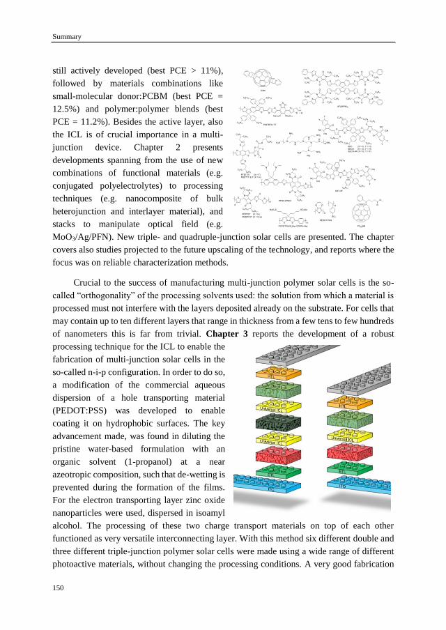
The first problem which was tackled was the development of a processing technique of
the ICL to fabricate inverted tandem and triple-junction solar cells with good versatility, i.e.
compatible with numerous chemically different active layer materials as subcells without the
need to constantly adopt choice of layers or choice of processing conditions to the specific
characteristics of the photoactive layer. The solution to this is provided in Chapter 3. Suitable
formulations of PEDOT:PSS and ZnO nanoparticles as charge transport materials in solvent
mixtures have been developed that allow for sufficient wetting and spreading during
deposition drying and at the same time fulfill the requirement of orthogonality, implying that
during deposition of the second layer, the first layer is not re-dissolved. In this way six
different tandem cells and three triple-junction solar cells involving a variety of active layers
could be made with the same ICL without adjusting the deposition conditions.
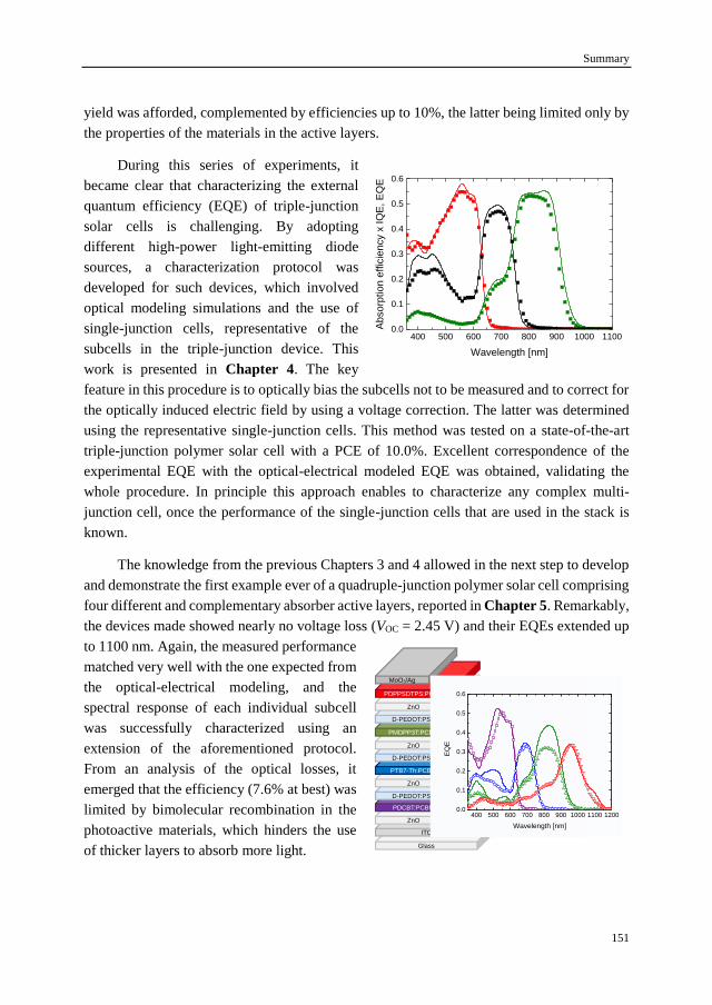
Triple-junction organic solar cells represent an intriguing kind of device for the high
efficiency they can achieve. In order to perform a correct characterization, the peculiarity of
OPV materials should be taken into account, to not overestimate the efficiency. Chapter 4
presents a detailed characterization protocol to fulfill this task, and shows the corresponding
results on a state-of-the-art triple-junction device with a PCE of 10.0%. The method used is
based on opto-electrical modeling simulations and measurements on representative single-
junction cells and provides an excellent match between experimental and modeled J−V and
EQE data.
To further extend the spectral response of triple-junction cells, another absorber
material was stacked on top of the back cell, with an ultralow band gap of ca. 1.1 eV. The
result, presented in Chapter 5, represents the first example ever reported of solution-
Chapter 1
14
processed quadruple-junction organic solar cell with four complementary absorber layers.
Opto-electrical modeling was involved to optimize the performance. The processing of the
ICL developed in Chapter 3 was used to interconnect all the subcells, and the characterization
protocol reported in Chapter 4 was extended to characterize the EQE of the four individual
subcells. The PCE of this cell equals 7.6%, only slightly less than the modeled value of 8.2%.
The versatile deposition technique reported in Chapter 3 allows to fabricate exclusively
inverted configuration devices. In a conventional device PEDOT:PSS would be processed on
top of a zinc oxide layer. Unfortunately the acidic dispersion from which PEDOT:PSS is
processed is not compatible with zinc oxide. In Chapter 6, commercial tin oxide colloidal
dispersions were combined with PEDOT:PSS to form new ICLs for tandems. Both
conventional and inverted tandem solar cells were manufactured with these materials, by
changing the sequence in which these were processed. Both tandem cell configurations
afforded PCEs of more than 10%.
Introduction
15
[1] United Nations. Department of Economic and Social Affairs, Population Division.
World Population Prospects: The 2017 Revision, Key Findings and Advance Tables.
Working Paper No. ESA/P/WP/248. 2017.
[2] J. Goldemberg, World energy assessment; United Nations Development
Programme: New York, NY, 2000.
[3] A. E. Becquerel, Comptes Rendus 1839, 9, 561.
[4] “April 25, 1954: Bell Labs Demonstrates the First Practical Silicon Solar Cell”. APS
News. American Physical Society. 18 (4). April 2009.
[5] D. M. Chapin, C. S. Fuller and G. L. Pearson, J. Appl. Phys. 1954, 25, 676.
[6] K. Yoshikawa, H. Kawasaki, W. Yoshida, T. Irie, K. Konishi, K. Nakano, T. Uto,
D. Adachi, M. Kanematsu, H. Uzu, K. Yamamoto, Nat. Energy 2017, 2, 17032.
[7] International Technology Roadmap for Photovoltaic Results 2017, Ninth edition,
March 2018.
[8] N. S. Lewis, Science 2007, 315, 798.
[9] National Renewable Energy Laboratory, Photovoltaic Efficiency chart, available at:
https://www.nrel.gov/pv/; accessed on 5 September 2018.
[10] M. A. Green, Third Generation Photovoltaics, Springer, 2003, ISBN: 3-540-40137-
7.
[11] C. K. Chiang, C. R. Fincher, Y. W. Park, A. J. Heeger, H. Shirakawa, E. J. Louis,
S. C. Gau, A. G. MacDiarmid, Phys. Rev. Lett. 1977, 39, 1098.
[12] H. Shirakawa, E. J. Louis, A. G. MacDiarmid, C. K. Chiang, A. J. Heeger, J. Am.
Chem. Soc., Chem. Commun. 1977, 16, 578.
[13] R. Søndergaard, M, Hösel, D. Angmo, T. T. Larsen-Olsen, F. Krebs, Mater. Today
2012, 15, 36.
[14] A. Reale, L. La Notte, L. Salamandra, G. Polino, G. Susanna, T. M. Brown, F.
Brunetti, A. Di Carlo, Energy Technol. 2015, 3, 385.
[15] M. Kaltenbrunner, M. S. White, E. D. Glowacki, T. Sekitani, T. Someya, N. S.
Sariciftci, S. Bauer, Nat. Commun. 2012, 3, 1772.
[16] R. Ma, J. Feng, D. Yin, H.-B. Sun, Org. Electron. 2017, 43, 77.
[17] Y. W. Li, G. Y. Xu, C. H. Cui, Y. F. Li, Adv. Energy Mater. 2018, 8, 1701791.
[18] K.-S. Chen, J.-F. Salinas, H.-L. Yip, L. Huo, J. Hou, A. K.-Y. Jen, Energy Environ.
Sci. 2012, 5, 9551.
[19] C.-C. Chen, L. Dou, J. Gao, W. H. Chang, G. Li, Y. Yang, Energy Environ. Sci.
2013, 6, 2714.
[20] J. Min, C. Bronnbauer, Z.-G. Zhang, C. Cui, Y. N. Luponosov, I. Ata, P. Schweizer,
T. Przybilla, F. Guo, T. Ameri, K. Forberich, E. Spiecker, P. Bäuerle, S. A.
Ponomarenko, Y. Li, C. J. Brabec, Adv. Funct. Mater. 2016, 26, 4543.
[21] D. Kearns, M. Calvin, J. Chem. Phys. 1958, 29, 950.
1.6 References
Chapter 1
16
[22] C. W. Tang, Appl. Phys. Lett. 1986, 48, 183.
[23] O. V. Mikhnenko, P. W. M. Blom, T.-Q. Nguyen, Energy Environ. Sci. 2015, 8,
1867.
[24] J. J. M. Halls, C. A. Walsh, N. C. Greenham, E. A. Marseglia, R. H. Friend, S. C.
Moratti, A. B. Holmes, Nature 1995, 376, 498.
[25] G. Yu, J. Gao, J. C. Hummelen, F. Wudl, A. J. Heeger, Science 1995, 270, 1789.
[26] S. Zhang, Y. Qin, J. Zhu, J. Hou, Adv. Mater. 2018, 30, 1800868.
[27] Z. Zheng, Q. Hu, S. Zhang, D. Zhang, J. Wang, S. Xie, R. Wang, Y. Qin, W. Li, L.
Hong, N. Liang, F. Liu, Y. Zhang, Z. Wei, Z. Tang, T. P. Russell, J. Hou, H. Zhou,
Adv. Mater. 2018, 30, 1801801.
[28] S. Li, L. Ye, W. Zhao, H. Yan, B. Yang, D. Liu, W. Li, H. Ade, J. Hou, J. Am. Chem.
Soc. 2018, 140, 7159.
[29] American Society for Testing and Materials (ASTM), Standard G173-03, available
at: http://rredc.nrel.gov/solar/spectra/am1.5/.
[30] W. Shockley, H. J. Queisser, J. Appl. Phys. 1961, 32, 510.
[31] S. Rühle, Sol. Energy 2016, 130, 139.
[32] A. De Vos, J. Phys. D: Appl. Phys. 1980, 13, 839.
[33] M. Hiramoto, M. Suezaki, M. Yokoyama, Chem. Lett. 1990, 19, 327.
[34] A. Yakimov, S. R. Forrest, Appl. Phys. Lett. 2002, 80, 1667.
[35] K. Triyana, T. Yasuda, K. Fujita, T. Tsutsui, Jpn. J. Appl. Phys. 2004, 43, 2352.
[36] J. Drechsel, B. Männig, F. Kozlowski, D. Gebeyehu, A. Werner, M. Koch, K. Leo,
M. Pfeiffer, Thin Solid Films 2004, 451–452, 515.
[37] B. Maennig, J. Drechsel, D. Gebeyehu, P. Simon, F. Kozlowski, A. Werner, F. Li,
S. Grundmann, S. Sonntag, M. Koch, K. Leo, M. Pfeiffer, H. Hoppe, D. Meissner,
N. S. Sariciftci, I. Riedel, V. Dyakonov, J. Parisi, Appl. Phys. A 2004, 79, 1.
[38] G. Dennler, H.-J. Prall, R. Koeppe, M. Egginger, R. Autengruber, N. S. Sariciftci,
Appl. Phys. Lett. 2006, 89, 073502.
[39] A. Colsmann, J. Junge, C. Kayser, U. Lemmer, Appl. Phys. Lett. 2006, 89, 203506.
[40] V. Shrotriya, E. H.-E. Wu, G. Li, Y. Yao, Y. Yang, Appl. Phys. Lett. 2006, 88,
064104.
[41] K. Kawano, N. Ito, T. Nishimori, J. Sakai, Appl. Phys. Lett. 2006, 88, 073514.
[42] J. Gilot, M. M. Wienk, R. A. J. Janssen, Appl. Phys. Lett. 2007, 90, 143512.
[43] J. Y. Kim, K. Lee, N. E. Coates, D. Moses, T.-Q. Nguyen, M. Dante, A. J. Heeger,
Science 2007, 317, 222.
[44] J. Gilot, M. M. Wienk, R. A. J. Janssen, Adv. Mater. 2010, 22, E67.
[45] L. Dou, J. You, J. Yang, C.-C. Chen, Y. He, S. Murase, T. Moriarty, K. Emery, G.
Li, Y. Yang, Nat. Photonics 2012, 6, 180.
[46] J. You, L. Dou, K. Yoshimura, T. Kato, K. Ohya, T. Moriarty, K. Emery, C.-C.
Chen, J. Gao, G. Li, Y. Yang, Nat. Commun. 2013, 4, 1446.
Introduction
17
[47] C.-H. Chou, W. L. Kwan, Z. Hong, L.-M. Chen, Y. Yang, Adv. Mater. 2011, 23,
1282.
[48] J. Yang, R. Zhu, Z. Hong, Y. He, A. Kumar, Y. Li, Y. Yang, Adv. Mater. 2011, 23,
3465.
[49] Y. Zhou, C. Fuentes-Hernandez, J. W. Shim, T. M. Khan, B. Kippelen, Energy
Environ. Sci. 2012, 5, 9827.
[50] J. Jo, J.-R. Pouliot, D. Wynands, S. D. Collins, J. Y. Kim, T. L. Nguyen, H. Y. Woo,
Y. Sun, M. Leclerc, A. J. Heeger, Adv. Mater. 2013, 25, 4783.
[51] D. W. Zhao, X. W. Sun, C. Y. Jiang, A. K. K. Kyaw, G. Q. Lo, D. L. Kwong, IEEE
Electron Device Lett. 2009, 30, 490.
[52] Y. Zou, Z. Deng, W. J. Potscavage, M. Hirade, Y. Zheng, C. Adachi, Appl. Phys.
Lett. 2012, 100, 243302.
[53] J. Gilot, Polymer Tandem Solar Cells, Ph.D. thesis, Eindhoven University of
Technology, 2010, ISBN: 978-90-386-2279-8.
[54] Heliatek, available at: http://heliatek.com.
[55] S. Esiner, H. Van Eersel, M. M. Wienk, R. A. J. Janssen, Adv. Mater. 2013, 25,
2932.
[56] W. Li, A. Furlan, K. H. Hendriks, M. M. Wienk, R. A. J. Janssen, J. Am. Chem. Soc.
2013, 135, 5529.
[57] C.-C. Chen, W.-H. Chang, K. Yoshimura, K. Ohya, J. You, J. Gao, Z. Hong, Y.
Yang, Adv. Mater. 2014, 26, 5670.
[58] R. Timmreck, T. Meyer, J. Gilot, H. Seifert, T. Mueller, A. Furlan, M. M. Wienk,
D. Wynands, J. Hohl-Ebinger, W. Warta, R. A. J. Janssen, M. Riede, K. Leo, Nat.
Photonics 2015, 9, 478.
[59] J. Gilot, M. M. Wienk, R. A. J. Janssen, Adv. Funct. Mater. 2010, 20, 3904.
[60] A. J. Moulé, K. Meerholz, Appl. Phys. Lett. 2007, 91, 061901.
[61] C. Duan, A. Furlan, J. J. van Franeker, R. E. M. Willems, M. M. Wienk, R. A. J.
Janssen, Adv. Mater. 2015, 27, 4461.
Chapter 2
Recent Developments on Solution-Processed
Multi-Junction Organic Solar Cells*
Abstract
This chapter offers an overview of the recent (2015 to mid-2018) developments in the
field of solution-processed multi-junction organic solar cells. In this time lapse different
strategies have been investigated to improve the performance of these devices. An important
one involves the development of new materials and processing methods for the photoactive
layers and the interconnecting layers. In addition, specific layers or combinations thereof
have been conveniently adopted to increase light absorption and improve the photocurrent
by utilizing optical interference effects that play a key role in these multi-junction
semitransparent thin layer stacks. Together with the increase in power conversion efficiency,
accurate characterization procedures are required to keep a critical view on the results and
new insights in this matter are discussed. Application of multi-junction cells for
photoelectrochemical water splitting and upscaling towards a commercial technology are
briefly addressed.
* This chapter has been submitted for publication as part of: D. Di Carlo Rasi, R. A. J.
Janssen. Advances in Solution-Processed Multi-Junction Organic Solar Cells.
Chapter 2
20
2.1 Introduction
In this chapter recent developments in the field of solution-processed organic tandem
solar cells are discussed.† The topic was last reviewed in 2015 and since then significant
progress has been made.[1-8] The materials forming the interconnecting layer (ICL) are key to
the optimal performance of tandem cells. The ICL serves to connect the subcells, both
optically and electrically, preferably without losses. Optical transparency, uniformity,
mechanical robustness, solvent orthogonality during processing, matching with the relevant
HOMO and LUMO levels and Ohmic character are important requisites that the ICL has to
fulfill. Besides the specific materials choice, the processing of the ICL from a liquid medium
plays a decisive role in the success of manufacturing the multi-layer stacks. Co-solvents,
additives, blends, and deposition techniques in general are commonly explored factors to
tweak the characteristics of the ICL. Because the absorber and ICL films are semitransparent
thin layers, interference effects play an important role in the distribution of the optical electric
field in the subcells and in turn in the absorption of light and the generated photocurrent.
Different approaches like the insertion of a thin reflecting materials inside the ICL can alter
the distribution of the optical field, to achieve a better balance in current generation. As
discussed in Chapter 1, tandem solar cells require photoactive materials with different band
gaps. In the context of solution-processed organic photovoltaic (OPV), the absorbers consists
of semitransparent thin films which can have a substantial overlap of their absorption spectra.
Hence, in addition to having different band gaps, photoactive layers should preferably also
have complementary absorption spectra, such that high energy photons that pass the first
layer are not absorbed in the second layer and are reflected at the back electrode. The optimal
thickness of single-junction cells is known to be limited by bimolecular recombination.
Developing photoactive absorber blends with thickness-insensitive performance can alleviate
the disadvantages of spectral overlap between the two subcells and increase the photocurrent.
Moreover, a high external quantum efficiency (EQE) is a prerequisite to absorb the incident
photons and increase the short-circuit current density (JSC). To afford a high open-circuit
voltage (VOC) tandem, both the subcells should possess a low minimum photon energy loss
(Eloss), defined as the difference between their optical band gap (Eg) and eVOC. Recombination
mechanisms should also be kept under control mainly via the creation of a suitable blend
morphology. A significant part of this chapter addresses recent developments of tandem solar
cells where new combinations of photoactive materials are presented. Although not yet
mature for the market, solution-processed tandem OPV technology was studied also related
to industry-oriented aspects such as the processing under ambient atmosphere, the increase
† The results presented in this chapter are largely based on a search on Web of Science, using the keywords:
“TI=((tandem OR triple* OR (multi*junction*) OR (multi-junction*)) AND (organic OR polymer OR (small
molecul*) OR (non-fullerene) OR (*fullerene*) OR (*fullerene-)) AND ((solar cell*) OR photovoltaic* OR
(photovoltaic cell*))) AND PY=(2015-2018)”, limited to the period from January 2015 to August 2018. Articles about hybrid tandem solar cells, articles where no actual device was fabricated and out-of-topic entries were
excluded.
Recent Developments on Solution-Processed Multi-Junction Organic Solar Cells
21
in device area by interconnecting more tandem cells to make a module, and the processing
from solution of the electrodes. The combination of more than two absorbers in solution-
processed multi-junction solar cells is still object of research, aiming at a further increase in
efficiency with respect to tandems. Overall, the reliability of the OPV field hinges on accurate
characterization protocols, taking into account the peculiarities of organic photovoltaic
materials. A detailed protocol for this was published at the beginning of the time period
covered here, and a brief analysis of how researchers now use the protocol is presented. Some
newly-developed exotic device stacks that do not fall in the category of tandems are included.
Besides the clear interest in increasing the power conversion efficiency (PCE) over that of
single-junction devices, specific applications can be identified where the properties of OPV
tandem cells turn advantageous. Photoelectrochemical water splitting is one of them, because
OPV tandem cells can provide the necessary voltage at the operating point. This voltage
should exceed the standard potential of 1.23 V for the water splitting reaction plus the
overpotentials at the electrodes. Conclusive general considerations complete the chapter. An
overview of the relevant features of the tandem cells published in the covered period is
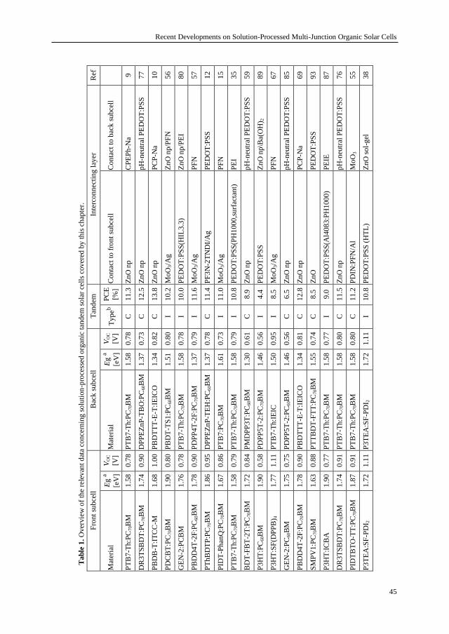
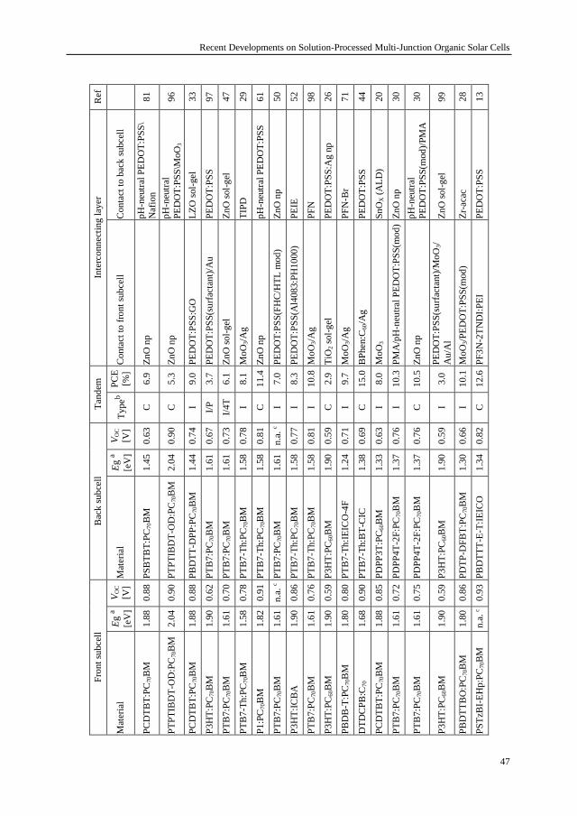
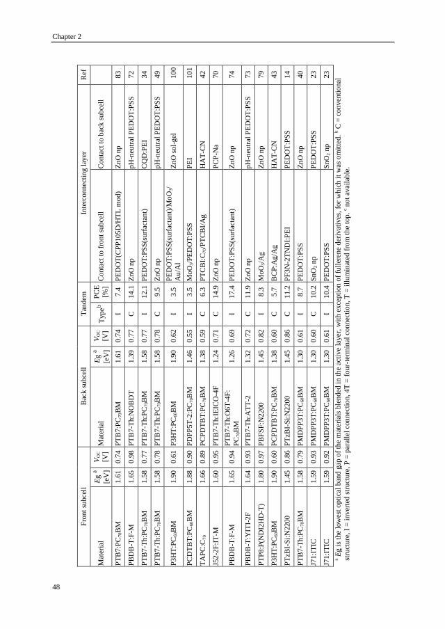
collected in Table 1.
2.2 Tandem solar cells
2.2.1 ICL materials
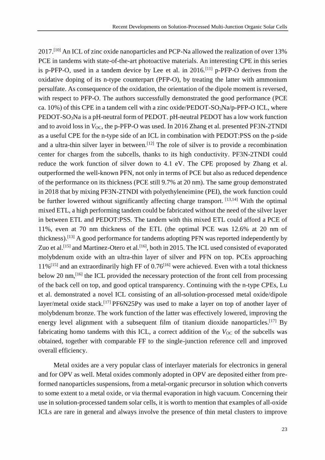
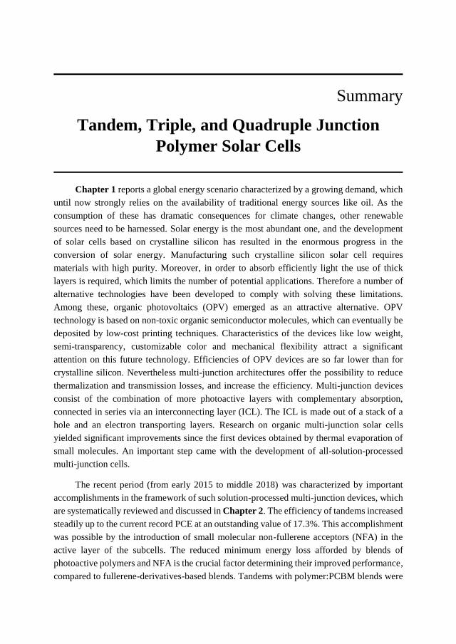
The ICL generally consists of combinations of polymeric and metal oxide materials.
Poly(3,4-ethylenedioxythiophene):polystyrene sulfonate (PEDOT:PSS) as hole transporting
layer (HTL) and zinc oxide nanoparticles as electron transporting layer (ETL) remain a
widely adopted combination of materials. From Table 1, it emerges that also evaporated
molybdenum oxide (HTL), followed by a thin (discontinuous) layer of silver and poly[(9,9-
bis(3′-(N,N-dimethylamino)propyl)-2,7-fluorene)-alt-2,7-(9,9-dioctylfluorene)] (PFN) as
ETL are frequently used. Nevertheless, several new materials have been introduced in recent
years. Especially, conjugated polyelectrolytes (CPE) and structurally related pH-neutral self-
doped conductive polymers (SCPs) are a largely explored alternative both for the p- as well
as for the n-type charge transporting layers. Decorating a conjugated polymer with anionic
or cationic side groups can create dipole moments that change the work function of the
substrate on which they are coated. The CPEs are often wide band gap semiconducting
materials that serve to change the work function. CPEs and SCPs are typically used as thin
layers (< 25 nm) to reduce parasitic light absorption. Generally, CPEs are processed from
alcoholic solvents because these are compatible with most of the tandem stacks. Figure 1
provides the chemical structure of the materials discussed hereafter.
Chapter 2
22
Figure 1. Materials adopted in the ICL of tandem solar cells covered by this chapter. The
references for publications using these materials are provided in Table 1.
In 2015, Zhou et al. presented two new CPEs: PCPDTBTSO3K (CPE-K) and
PCPDTPhSO3Na (CPEPh-Na).[9] Owing to the ionic side groups, a thin layer (10−15 nm) of
these p-type materials could effectively increase the work function of the substrate to 5.2 eV.
Tandem devices using a zinc oxide nanoparticles layer coated with CPEPh-Na as ICL showed
PCE up to 11.3%. Structurally similar is the p-type CPE PCP-Na, adopted by Cui et al. in
Recent Developments on Solution-Processed Multi-Junction Organic Solar Cells
23
2017.[10] An ICL of zinc oxide nanoparticles and PCP-Na allowed the realization of over 13%
PCE in tandems with state-of-the-art photoactive materials. An interesting CPE in this series
is p-PFP-O, used in a tandem device by Lee et al. in 2016.[11] p-PFP-O derives from the
oxidative doping of its n-type counterpart (PFP-O), by treating the latter with ammonium
persulfate. As consequence of the oxidation, the orientation of the dipole moment is reversed,
with respect to PFP-O. The authors successfully demonstrated the good performance (PCE
ca. 10%) of this CPE in a tandem cell with a zinc oxide/PEDOT-SO3Na/p-PFP-O ICL, where
PEDOT-SO3Na is a pH-neutral form of PEDOT. pH-neutral PEDOT has a low work function
and to avoid loss in VOC, the p-PFP-O was used. In 2016 Zhang et al. presented PF3N-2TNDI
as a useful CPE for the n-type side of an ICL in combination with PEDOT:PSS on the p-side
and a ultra-thin silver layer in between.[12] The role of silver is to provide a recombination
center for charges from the subcells, thanks to its high conductivity. PF3N-2TNDI could
reduce the work function of silver down to 4.1 eV. The CPE proposed by Zhang et al.
outperformed the well-known PFN, not only in terms of PCE but also as reduced dependence
of the performance on its thickness (PCE still 9.7% at 20 nm). The same group demonstrated
in 2018 that by mixing PF3N-2TNDI with polyethyleneimine (PEI), the work function could
be further lowered without significantly affecting charge transport. [13,14] With the optimal
mixed ETL, a high performing tandem could be fabricated without the need of the silver layer
in between ETL and PEDOT:PSS. The tandem with this mixed ETL could afford a PCE of
11%, even at 70 nm thickness of the ETL (the optimal PCE was 12.6% at 20 nm of
thickness).[13] A good performance for tandems adopting PFN was reported independently by
Zuo et al.[15] and Martinez-Otero et al.[16], both in 2015. The ICL used consisted of evaporated
molybdenum oxide with an ultra-thin layer of silver and PFN on top. PCEs approaching
11%[15] and an extraordinarily high FF of 0.76[16] were achieved. Even with a total thickness
below 20 nm,[16] the ICL provided the necessary protection of the front cell from processing
of the back cell on top, and good optical transparency. Continuing with the n-type CPEs, Lu
et al. demonstrated a novel ICL consisting of an all-solution-processed metal oxide/dipole
layer/metal oxide stack.[17] PF6N25Py was used to make a layer on top of another layer of
molybdenum bronze. The work function of the latter was effectively lowered, improving the
energy level alignment with a subsequent film of titanium dioxide nanoparticles.[17] By
fabricating homo tandems with this ICL, a correct addition of the VOC of the subcells was
obtained, together with comparable FF to the single-junction reference cell and improved
overall efficiency.
Metal oxides are a very popular class of interlayer materials for electronics in general
and for OPV as well. Metal oxides commonly adopted in OPV are deposited either from pre-
formed nanoparticles suspensions, from a metal-organic precursor in solution which converts
to some extent to a metal oxide, or via thermal evaporation in high vacuum. Concerning their
use in solution-processed tandem solar cells, it is worth to mention that examples of all-oxide
ICLs are rare in general and always involve the presence of thin metal clusters to improve
Chapter 2
24
their conductivity.[18,19] Only in 2018 Becker et al. reported the first all-oxide ICL for polymer
tandem solar cells.[20] A possible reason for the scarcity of such examples might be because
very few materials (like PEDOT:PSS) can guarantee the protection of the front cell active
layer against the processing from solution of the back cell active layer.[21] The exceptional
example of Becker et al. consisted of an inverted (n-i-p) configuration tandem in which
thermally evaporated molybdenum oxide (HTL) and tin oxide (ETL) deposited via atomic
layer deposition were stacked together to form the ICL. Together with the singular protection
against solvents, the authors indicated that a large intrinsic interface dipole at the interface
HTL/ETL makes the conduction bands of molybdenum oxide and tin oxide to align. In
addition, the tandem featuring this ICL did not suffer from the well-known problem of
necessity of UV light soaking. In fact, it is known that exposing common conductive metal
sub-oxides, such as zinc oxide and titanium dioxide, to UV light illumination can increase
their conductivity by a photodoping mechanism.[ 22 ] In Chapter 6, the use of solution-
processable tin oxide nanoparticles suspensions for OPV tandems is presented for the first
time.[23] In combination with PEDOT:PSS as HTL, both conventional (p-i-n) and inverted
architecture tandems were realized using only these two materials, with performance in good
agreement with the expectations. For conventional tandems tin oxide offers the possibility to
avoid the use of pH-neutral PEDOT:PSS, which can cause a loss in VOC due its reduced work
function. In fact, tin oxide proved to be resistant against the acidity of the commercial
formulation of PEDOT:PSS (Al 4083), while zinc oxide is washed away. In 2015 Mitul et al.
implemented solution-processed aluminum-doped zinc oxide (AZO) in a
PEDOT:PSS/AZO/PEIE ICL, where PEIE is the partially ethoxylated polyethyleneimine.[24]
Thermal annealing at 150 °C was required to form AZO from its precursor. To demonstrate
the proper working of this ICL, the authors built a homo tandem using P3HT:PCBM, which
can sustain this temperature. In 2017 Du et al. reported molybdenum oxide nanoparticles as
a solution to overcome interfacial losses occurring in some tandem solar cells where
PEDOT:PSS is used as HTL.[25] They attributed poor hole transporting properties of the
interface between PEDOT:PSS and an active layer with polymers containing nitrogen atoms
to the protonation of the latter. By mixing PEDOT:PSS and MoO3 nanoparticles, the problem
was reported to be solved and tandem solar cells using a PEDOT:PSS:MoO3/ZnO/PEI ICL
showed improved performance compared to the control tandem devices with only
PEDOT:PSS or MoO3. Concerning composite materials with PEDOT:PSS, Torabi et al.
reported in 2015 a mixture of modified PEDOT:PSS and silver nanoparticles as HTL in the
ICL, in combination with sol-gel titanium dioxide as ETL.[26] The silver nanoparticles were
synthesized directly in the dispersion of the modified PEDOT:PSS by reduction of the silver
nitrate precursor with sodium borohydride, without the need of a stabilizer. A homo tandem
was realized to check the performance. The VOC was 1.1 V and the FF 0.60, against the 0.59
V and FF of 0.55 of the reference cell.
Recent Developments on Solution-Processed Multi-Junction Organic Solar Cells
25
Recently, few examples of tandem solar cells have emerged in which metal-organic
compounds have been adopted in the ICL. Lu et al. in 2016[27] and Chang et al. in 2017[28]
adopted zirconium acetylacetonate (Zr-acac) to lower the work function of PEDOT:PSS in
the ICLs: PEDOT:PSS/Zr-acac/PF6N25Py and MoO3/PEDOT:PSS/Zr-acac, respectively.
Zr-acac has the advantage that it can be easily processed from solution and does not require
a thermal annealing treatment. Another example of metal chelate in tandems was published
in 2018 by Shi et al.[29] In their work, Shi et al. used titanium (diisopropoxide)bis(2,4-
pentanedionate (TIPD) on top of evaporated MoO3/Ag as ICL, applying a post-treatment of
150 °C to get the optimal performance of the tandem. A single example of an inorganic
transition metal compound for tandem applications is represented by the phosphomolybdic
acid hydrate (PMA), presented by Lu et al. in 2017 in both conventional and inverted
structure tandems.[30] In their work, a modified pH-neutral PEDOT:PSS layer served as
recombination center for the charges extracted by the PMA HTL and the zinc oxide
nanoparticles ETL. The ICL was then PMA/PEDOT:PSS/ZnO in inverted tandems and vice
versa for the conventional ones. As will be discussed in more detail in Chapter 6, the work
function of pH-neutral PEDOT:PSS does not match the deep-lying HOMO energy level of
some photoactive polymers, generally provoking a loss in VOC.[31] By using PMA in between
pH-neutral PEDOT:PSS and the active layer of P3HT:PC60BM the authors showed a
recovery in the VOC with respect to the control device without PMA (0.62 V vs 0.48 V,
respectively).
Concerning the use allotropic forms of carbon in the ICL, three examples have been
reported in the last period. In 2015 Chang et al. used a cross-linkable azidofullerene
derivative ((C-)PCBN3), doped with tetrabutylammonium iodide (TBAI) as ETL, on top of
PEDOT:PSS.[32] A temperature of 140 °C was used for the curing of the ETL, which allowed
the manufacturing of tandems on a flexible polyethylene naphthalate substrate with good
performance (PCE of 8.7% vs 9.3% on glass). The ETL showed also a weak thickness
dependence of the performance, with an optimum at 10 nm. A mixture of PEDOT:PSS and
graphene oxide has been reported to work in an ICL, together with lithium-doped zinc oxide
(LZO) as ETL, in a publication published in 2015 by da Silva et al.[33] Another form of carbon
for the ICL are carbon quantum dots (CQDs), mixed with PEI described by Kang et al. in
2018.[34] CQDs were synthesized by a microwave reaction starting from citric acid and β-
alanine, resulting in particles with size of ca. 3 nm. A thin layer of the CQDs/PEIE composite
on top of PEDOT:PSS was reported to provide an efficient tunneling junction for the
recombination of charges in the ICL, affording a best efficiency of 12.1%.
2.2.2 Processing multi-junction stacks
For the commercial success of future tandem OPV technology is important to simplify
the manufacturing processes as much as possible. In this section recent advances focusing on
processing of tandem OPV cells are reported.
Chapter 2
26
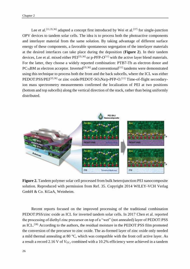
Lee et al.[11,35,36] adapted a concept first introduced by Wei et al.[37] for single-junction
OPV devices to tandem solar cells. The idea is to process both the photoactive components
and interlayer material from the same solution. By taking advantage of different surface
energy of these components, a favorable spontaneous segregation of the interlayer materials
at the desired interfaces can take place during the deposition (Figure 2). In their tandem
devices, Lee et al. mixed either PEI[35,36] or p-PFP-O[11] with the active layer blend materials.
For the latter, they choose a widely reported combination: PTB7-Th as electron donor and
PC70BM as electron acceptor. Inverted[35,36] and conventional[11] tandems were demonstrated
using this technique to process both the front and the back subcells, where the ICL was either
PEDOT:PSS/PEI[35,36] or zinc oxide/PEDOT-SO3Na/p-PFP-O.[11] Time-of-flight secondary-
ion mass spectrometry measurements confirmed the localization of PEI at two positions
(bottom and top subcells) along the vertical direction of the stack, rather than being uniformly
distributed.
Figure 2. Tandem polymer solar cell processed from bulk heterojunction:PEI nanocomposite
solution. Reproduced with permission from Ref. 35. Copyright 2014 WILEY-VCH Verlag
GmbH & Co. KGaA, Weinheim.
Recent reports focused on the improved processing of the traditional combination
PEDOT:PSS/zinc oxide as ICL for inverted tandem solar cells. In 2017 Chen et al. reported
the processing of diethyl zinc precursor on top of a “wet” (not annealed) layer of PEDOT:PSS
as ICL.[38] According to the authors, the residual moisture in the PEDOT:PSS film promoted
the conversion of the precursor to zinc oxide. The as-formed layer of zinc oxide only needed
a mild thermal annealing at 80 °C, which was compatible with the front cell active layer. As
a result a record 2.16 V of VOC, combined with a 10.2% efficiency were achieved in a tandem
Recent Developments on Solution-Processed Multi-Junction Organic Solar Cells
27
device, demonstrating the good functioning of the ICL. Given the hydrophobic nature of
commonly adopted active layer materials, the deposition of a layer of PEDOT:PSS from an
aqueous dispersion requires the use of surfactants to lower the surface energy. Surfactants
are in general insulating and the amount of them necessary to improve the casting can
eventually be substantial and deteriorate the desired properties of PEDOT:PSS. Moreover,
modifying PEDOT:PSS might affect unfavorably the distribution of the insulating PSS part,
creating an energy barrier. In 2016 Prosa et al. proposed a simple approach to recover the
good functioning of a PEDOT:PSS film deposited from a suspension including a surfactant
(Zonyl FS-300).[39] By simply rinsing the film with isopropanol, part of the surfactant and the
excess of PSS at the surface of the layer could be removed. Tandems with isopropanol-rinsed
PEDOT:PSS, followed by zinc oxide nanoparticles as ICL demonstrated optimal
performance, contrary to the pristine device with non-rinsed PEDOT:PSS. In fact, the latter
featured an s-shape in the J–V characteristics, likely denoting the presence of an interfacial
barrier. The results discussed in the Chapter 3 of this thesis[40] demonstrate how both the
requirements of a low annealing temperature of the ICL and a low surface energy of the
PEDOT:PSS dispersion can be satisfied at the same time. It was found that by processing in
inert atmosphere the commercial formulation of PEDOT:PSS (Al4083) from a mixture of
water/1-propanol (1:2 v/v) provides a good coverage for a wide selection of different active
layer materials, without the need of a surfactant. A synthetic procedure of zinc oxide
nanoparticles was also reported, and isoamyl alcohol was adopted as liquid for the dispersion.
The processing of zinc oxide from such suspension did not negatively affect the PEDOT:PSS
layer. Without any thermal annealing treatment, the proposed processing technique afforded
six tandems and three triple-junction solar cells featuring eight active layer materials of
different chemical nature. Using the same technique, the first example of a solution-processed
quadruple-junction polymer solar cell with four complementary absorber layers was reported,
discussed in detail in Chapter 5.[41]
Orthogonality of the solutions is a stringent requirement for fabricating complex device
stacks such as tandems directly from solution. A possible way to get around this constraint is
to stamp transfer the top subcell, avoiding the use of solvents. In 2017 Ka et al. demonstrated
an example of device fabricated in this fashion. In their work they deposited a front cell
consisting of the small molecular donor TAPC blended with C70.[42] Next in the stack they
deposited, also by thermal evaporation, a PTCBI:C70 buffer electron transport layer,
preceding a PTCBI/Ag/HAT-CN interconnecting layer. For the back cell they adopted
PCPDTBT:PC70BM, which has a low band gap of 1.38 eV. The latter was deposited by spin-
coating onto a poly(dimethylsiloxane) stamp, dried in high vacuum from solvents, coated
onto the evaporated front subcell/ICL stack and detached from the stamp after annealing at
100 °C under applied pressure, to form a conformal contact at the interface. The resulting
tandem was characterized by a correct addition of the VOC of the subcells: this was 0.89 and
0.59 V for the front and the back subcells respectively, while for the tandem 1.46 V of VOC
Chapter 2
28
was measured. Maybe due to the limited FF of both the single-junction cells, the tandem
featured a FF of only 0.51, limiting the efficiency to 6.26%. Later, in 2018 Ka et al. also
demonstrated a polymer tandem solar cell where both the front and the back subcells were
deposited by stamp transfer and the interlayers were obtained by thermal evaporation.[43]
P3HT:PC60BM was adopted in the front cell and PCPDTBT:PC70BM as back cell. The
tandem showed full addition of the VOC (1.20 V) and a FF of 0.60. In 2018, Che et al. revisited
the same concept of combining a thermally evaporated front cell together with a solution-
processed back cell.[44] Differently from the work discussed before, the back subcell was
directly deposited by spin-coating on top of the evaporated front subcell. The former was a
DTDCPB:C70 co-evaporated cell, coated with ETL BPhen:C60/Ag, also by thermal
evaporation. Following, PEDOT:PSS was cast to complete the ICL, and the back cell of
PTB7-Th:BT-CIC was deposited by spin-coating. The front cell donor material has a wide
band gap of 1.68 eV, while donor and acceptors in the back cell have band gaps of 1.58 and
1.38 eV, respectively. An outstanding high PCE of 15 % was obtained by this tandem cell,
arising from an EQE between 70% and 80%, corresponding to a measured JSC of 12.7 mA
cm−2. By applying an antireflection coating on the glass facade the JSC increased even further,
up to 13.3 mA cm−2. In addition, the VOC of 1.59 V followed the sum of the constituent
subcells (0.90 and 0.69 V for the front and back cells, respectively), together with a high FF
of 0.71. Another remarkable aspect of this work is the high yield accompanying the high
efficiency: 97% and 95% for solar cells with active area of 2 and 9 mm2, from a total of 130
devices.
2.2.3 Light management
Organic multi-junction solar cells feature stacks of several semitransparent thin films.
For such kind of devices, optical interference effects play an important role, reason for which
a number of papers have focused their attention on how to take advantage of these effects, in
order to improve the balance of absorption of light from the two subcells. In 2015 Zuo et al.
explored the influence of the thickness of the Ag layer in a MoO3/Ag/PFN ICL on the balance
of current from the subcells.[15] In particular, an optical micro-cavity is formed between the
thin silver layer in the ICL (8−14 nm) and the opaque silver contact on the back cell (Figure
3).
Recent Developments on Solution-Processed Multi-Junction Organic Solar Cells
29
Figure 3. Micro-cavity tandem polymer solar cell. Device scheme (a), cartoon
illustrating the micro-cavity enhancement in the back cell (b), and modeled EQE spectra of
the subcells as function of the thickness of the Ag layer in the ICL. Reproduced with
permission of RSC, from Ref. 15 conveyed through Copyright Clearance Center, Inc.
By acting on the thickness of the thin silver layer, the balance of absorption between
front and back subcells could be tuned to achieve current matching. Moreover, the authors
were able to measure the individual subcells directly by accessing externally the intermediate
silver contact. A similar phenomenon was observed in tandem cells with parallel-connection
by Lee et al. in 2015[45] and Zuo et al. in 2017.[46] In the first case MoO3/Ag/MoO3 was the
ICL, while in the second case it was PEDOT:PSS/Ag/Au/MoO3. In a parallel-connection
tandem the requirement of current matching drops, since the total current is the summation
of the current of the subcells. Besides the increase in current, the voltage is pinned to the
lowest voltage between the two subcells. Due to the limited charge mobility in most of the
organic semiconductors, the optimal thickness of a single-junction device is usually
determined by the tradeoff between increasing charge generation by more light absorption in
thicker layers and the concomitant decrease because of bimolecular charge recombination.
To increase light absorption while preserving the fill factor (influenced by charge
recombination), the same active layer absorber can be deposited twice in a homo tandem.
The one reported by Zuo et al. in particular, represented at the time the most efficient example
for organic tandem solar cell with parallel connection (PCE of 11.1%). PTB7-Th:4TIC was
used as active layer. Again to improve the absorption of active layers suffering from
thickness-dependent performance, in 2015 Mantilla-Perez et al. fabricated a four-terminal
homo-tandem solar cell.[47] A glass substrate coated with indium-doped tin oxide (ITO) on
both sides was used to build single-junction cells on each side (Figure 4a).
(a) (b) (c)
Chapter 2
30
Figure 4. Four-terminal tandem (a) and top-illuminated tandem with DMD electrode (b).
Reprinted with permission from Ref. 47 (Copyright (2015) American Chemical Society) and
with permission of RSC from Ref. 48 (conveyed through Copyright Clearance Center, Inc).
As transparent electrode, a dielectric-metal-dielectric (DMD) electrode was deposited
by thermal evaporation on top of one of the active layers, consisting of MoO3/Ag/MoO3. The
top electrode on the other subcell was an opaque metal. Another advantage of this special
architecture is that the two subcells can be operated independently, which solves the
requirement of current or voltage matching. As stressed by the authors, a limiting factor in
their particular device was the DMD electrode, due to its poor transparency. Related to this
point, Zuo et al. reported in 2016 a series-connected tandem solar cell featuring a
MoO3/Ag/TeO2 DMD transparent top electrode.[48] The device was built starting from an
opaque silver layer on glass as bottom electrode, and finished with the DMD stack on top
(Figure 4b). Interestingly, the DMD tandem had a performance close to the ITO-based
counterpart, thanks to the TeO2 capping layer, which reduced the reflection at the thin silver
layer, the first one encountered by light. Another way to enhance the absorption of the active
layers was reported in 2018 by Mayer et al.[49] Here a templated periodical structure was
applied externally on the glass side of an ITO-based tandem solar cell. The structure reported
was made with a UV-curable polymer on a glass substrate and a master template fabricated
with laser interference lithography. A relative increase by 9% in the PCE was recorded
following the application of this diffractive structure.
Optical interference in tandem solar cells is usually optimized considering illumination
in the direction perpendicular to the surface of the device. Nevertheless, in practical scenarios
the solar cell is not constantly oriented in such direction but there is rather a certain angle of
incidence. In 2016 Mertens et al.[50] tried to understand a peculiar behavior of organic tandem
(a) (b)
Recent Developments on Solution-Processed Multi-Junction Organic Solar Cells
31
solar cells, already reported by Riede et al.[51] for evaporated tandem cells in 2011. In detail,
when their device was at a certain angle of orientation Θ with respect to the direction of
incidence of light, the short-circuit current density corrected by the effective area of
illumination (J*SC=JSC/cos(Θ)) was relatively insensitive to this angle, up to 65°.[50] In their
work, the authors showed that both the measured and modeled EQE spectra of the individual
subcells change according to Θ. Nevertheless, both of the corresponding spectrally integrated
J*SCs stay relatively constant. The angle-insensitivity of the performance of organic tandem
solar cells is particularly interesting for their application in realistic operating conditions.
In order for tandem organic solar cells to succeed in their commercialization, appealing
characteristics like the possibility to easily tune their color are very important. In 2017 Luo
et al. reported flexible all-solution-processed polymer tandem solar cells with different
colors.[52] Thanks to the highly conductive PEDOT:PSS top electrode, the reflectivity of the
device was engineered by simply changing the thickness of it. PCE values from 7.23 to 8.34%
were achieved, corresponding to different colors.
2.2.4 Active layer materials
In order to exploit the full potential of tandem solar cells, the active layer materials need
to be engineered to absorb light in complementary regions of the solar spectrum. A number
of materials, either newly developed or previously reported in single-junction devices, have
been adopted in tandem solar cells for this purpose. For a complete list of photoactive
materials, either small molecules or polymers, and their optical gap, the reader should refer
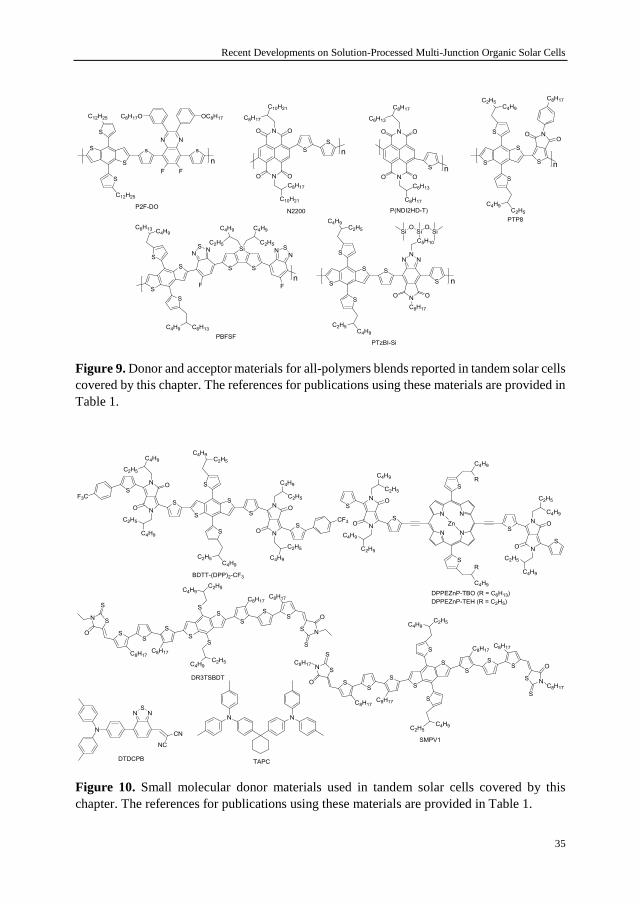
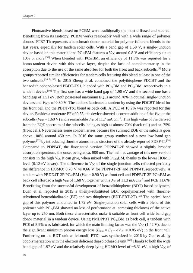
to Table 1. Figures 5-10 show their chemical structure.
Figure 5. Fullerene acceptors used in tandem solar cells covered by this chapter. The
references for publications describing these materials are provided in Table 1.
Chapter 2
32
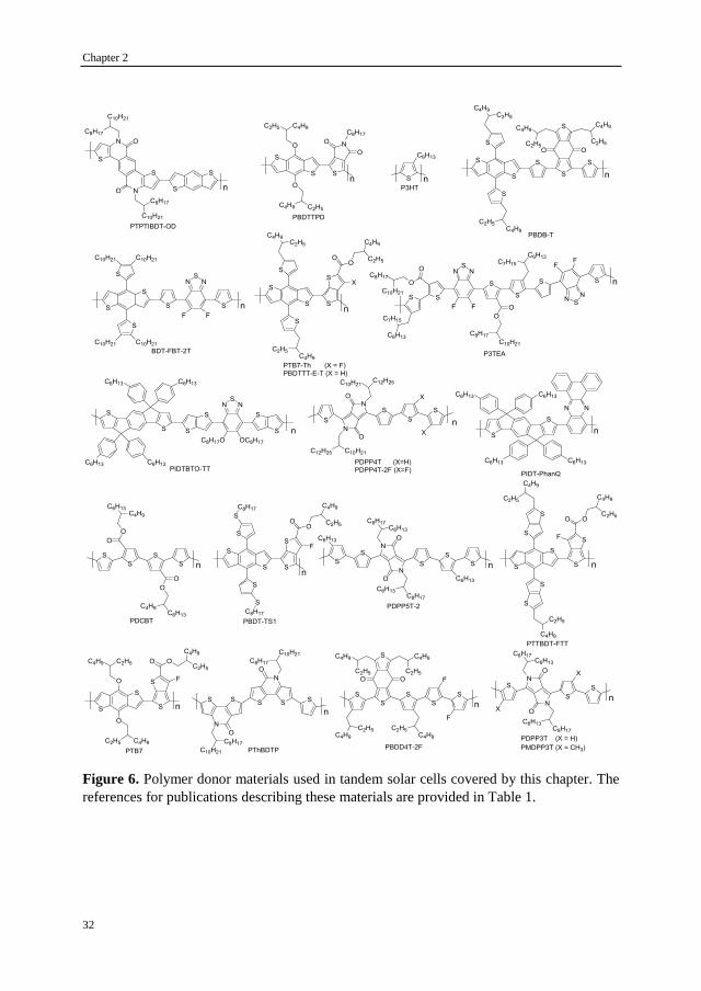
Figure 6. Polymer donor materials used in tandem solar cells covered by this chapter. The
references for publications describing these materials are provided in Table 1.
Recent Developments on Solution-Processed Multi-Junction Organic Solar Cells
33
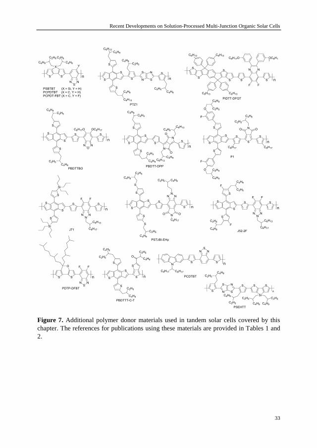
Figure 7. Additional polymer donor materials used in tandem solar cells covered by this
chapter. The references for publications using these materials are provided in Tables 1 and
2.
Chapter 2
34
Figure 8. Non-fullerene acceptor materials used in tandem solar cells covered by this chapter.
The references for publications using these materials are provided in Table 1.
Recent Developments on Solution-Processed Multi-Junction Organic Solar Cells
35
Figure 9. Donor and acceptor materials for all-polymers blends reported in tandem solar cells
covered by this chapter. The references for publications using these materials are provided in
Table 1.
Figure 10. Small molecular donor materials used in tandem solar cells covered by this
chapter. The references for publications using these materials are provided in Table 1.
Chapter 2
36
Photoactive blends based on PCBM were traditionally the most diffused and studied.
Benefiting from its isotropy, PCBM works reasonably well with a wide range of polymer
donors. PTB7-Th represents a benchmark donor material for polymer-fullerene blends in the
last years, especially for tandem solar cells. With a band gap of 1.58 V, a single-junction
device based on this material and PC70BM features a VOC around 0.8 V and efficiency up to
10% or more.[53] When blended with PC70BM, an efficiency of 11.3% was reported for a
homo-tandem device with this active layer, despite the lack of complementarity in the
absorption due to the use of the same absorber for both the front and back subcells.[9] More
groups reported similar efficiencies for tandem cells featuring this blend at least in one of the
two subcells.[34,54,55] In 2015 Zheng et al. combined the polythiophene PDCBT and the
benzodithiophene-based PBDT-TS1, blended with PC70BM and PC60BM, respectively in a
tandem device.[56] The first one has a wide band gap of 1.90 eV and the second one has a
band gap of 1.51 eV. Both possessed maximum EQEs around 70% in optimal single-junction
devices and VOCs of 0.80 V. The authors fabricated a tandem by using the PDCBT blend for
the front cell and the PBDT-TS1 blend as back cell. A PCE of 10.2% was reported for this
device. Besides a moderate FF of 0.55, the device showed a correct addition of the VOC of the
subcells (VOC = 1.60 V) and a remarkable JSC of 11.7 mA cm−2. This high value of JSC derived
from the EQE spectrum of the subcells, being as high as almost 70% (back cell) and ca. 75%
(front cell). Nevertheless some concern arises because the summed EQE of the subcells goes
above 100% around 450 nm. In 2016 the same group synthesized a new low band gap
polymer[57] by introducing fluorine atoms in the structure of the already reported PDPP4T.[58]
Compared to PDPP4T, the fluorinated version PDPP4T-2F showed a slightly broader
absorption spectrum, the onset being at ca. 900 nm. The main advantage of this new version
consists in the high VOC it can give, when mixed with PC60BM, thanks to the lower HOMO
level (0.12 eV lower). The difference in VOC of the single-junction cells reflected perfectly
the difference in HOMO: 0.78 V vs 0.66 V for PDPP4T-2F and PDPP4T, respectively. A
tandem with PBDD4T-2F:PC60BM (VOC = 0.90 V) as front cell and PDPP4T-2F:PC70BM as
back cell afforded a high VOC of 1.68 V, together with a JSC of 11.3 mA cm−2 and PCE 11.6%.
Benefitting from the successful development of benzodithiophene (BDT) based polymers,
Duan et al. reported in 2015 a thienyl-substituted BDT copolymerized with fluorine-
substituted benzothiadiazole (BT) and two thiophenes (BDT-FBT-2T).[59] The optical band
gap of this polymer amounted to 1.72 eV. Single-junction solar cells with a blend of this
polymer with PC70BM showed no loss of performance at increasing thickness of the active
layer up to 250 nm. Both these characteristics make it suitable as front cell wide band gap
donor material in a tandem device. Using PMDPP3T:PC60BM as back cell, a tandem with
PCE of 8.9% was fabricated, for which the main limiting factor was the VOC (1.42 V), due to
the significant minimum photon energy loss (Eloss = Eg – eVOC = 0.85 eV) in the front cell.
Furthering on the BDT unit as leitmotif, PTZ1 was synthesized in 2016 by Guo et al. by
copolymerization with the electron deficient thiazolothiazole unit.[60] Thanks to both the wide
band gap of 1.97 eV and the relatively deep-lying HOMO level of −5.31 eV, a high VOC of
Recent Developments on Solution-Processed Multi-Junction Organic Solar Cells
37
1.01 V was measured for the pristine PTZ1:PC70BM single-junction solar cell, which lowered
to 0.94 V after optimization of the processing conditions. These materials were adopted in a
tandem as front cell, with a blend of the low band gap (1.58 eV) PBDTTT-C-T and PC70BM
in the back cell. The latter was reported to give a VOC of 0.74 V. The measurement of the
tandem returned a PCE of 10.3%, with a nearly ideal addition of the VOC (1.65 V), FF of 0.65
and JSC of 9.6 mA cm−2. Integration of the EQE of the subcells returned 8.15 and 9.80 mA
cm−2 for the front and back subcells, respectively. Indacenodithiophene (IDT) is an
interesting donor unit for donor-acceptor (D-A) copolymers given the planarity of its
structure. A new copolymer of IDT with BT units was reported in 2017 by Ma et al.
(PIDTBTO-TT).[55] The authors copolymerized these units using thienothiophene (TT) as π-
bridges. After optimization of the morphology using PC70BM as acceptor and diiodooctane
as co-solvent, a PCE of 8.15% was recorded. Since the polymer had a band gap of 1.87 eV
and gave VOC of 0.91 V, it was used as front cell of a tandem, in combination with PTB7-
Th:PC70BM in the back cell. A VOC of 1.70 V and PCE of 11.2% were achieved for the best
device. More BDT-based donor polymers were reported by Song et al. in 2017, P1 and P2.[61]
For an optical band gap of 1.82 eV, 0.91 V and 1.00 V of VOC were achieved in single-
junction devices with PC70BM, thanks to deep-lying HOMO levels of −5.43 and −5.50 eV,
respectively. The single junctions were also characterized by EQE spectra of 70%. These
materials were used as front cell for two different tandem solar cells, in combination with
PTB7-Th:PC70BM (VOC = 0.81 V) in the back cell. From the measurements, VOC values of
1.64 (with P1) and 1.72 V (with P2) were achieved, respectively. The measured JSCs were
10.1 (P1) and 9.3 mA cm−2 (P2) and lower JSCs were integrated from the EQE spectra of the
subcells.
In recent years increasing focus in the OPV field is on non-fullerene acceptors
(NFAs).[62-65] NFA molecules allow more freedom to engineer the energy levels (and optical
band gap) to achieve high VOC. Different from fullerene-based acceptors, a reduced offset in
the HOMO-HOMO and LUMO-LUMO of donor and acceptor does not occur at the expense
of efficient charge separation.[66] Studies suggested a different nature of the exciton separation
process in this class of systems. In addition, the photocurrent can benefit from their
substantial absorption coefficient. Although the anisotropy limits the number of successful
donor-acceptor combinations, an increasing number of relevant results have been reported in
the last few years, with important consequences on the efficiency not only of single-junction
but also of tandem solar cells. The review paper by Cheng et al. provides a good picture of
recent results about non-fullerene polymer solar cells and the direction to further advance in
this field. Hou et al. also analyzed the opportunities and challenges of NFAs. For a more in-
depth discussion of the topic, the reader is referred to recent review papers.[62-65] A first
demonstration of how a high VOC can be achieved in tandems with NFAs was given by Liu
et al. in 2016.[67] Two polymer:NFA systems with high VOC and complementary absorption
were selected for their tandem: P3HT:SF(DPPB)4 (the band gaps are 1.90 and 1.77 eV,
Chapter 2
38
respectively) and PTB7-Th:IEIC (band gaps of 1.58 and 1.50 eV, respectively). The first one
delivered a VOC of 1.11 V, while the second one gave 0.95 V. The best tandem device (PCE
= 8.48%) afforded a VOC as high as 1.97 V. The performance in this case was mainly limited
by the FF (0.52), largely determined by the FF of the corresponding single-junction cells
(0.54 and 0.47 for the front and back subcells). The highest VOC for a NFA tandem was
reported in 2017 by Chen et al.[38] With P3TA (band gap = 1.72 eV) and SF-PDI2 (band gap
= 2.07 eV) as polymer donor and NFA, respectively, a low minimum voltage loss could be
achieved (0.6 eV). Due to the limited absorption in the optimal single-junction device,
combining the same active layer blend as both front and back subcells in a homo tandem
allowed to boost the efficiency from 9.5% (single junction) to 10.8% (tandem), accompanied
by a remarkable VOC of 2.13 V. In 2017 multiple NFA systems introduced in tandem solar
cells allowed to break the 12% efficiency threshold, surpassing the current state-of-the-art
for fullerene-based tandems. In 2017 Shi et al. reported an efficient low band gap NFA by
combining a central fused rings electron-donating unit, thiophene-thienothiophene-thiophene
(4T), with a terminal electron-accepting part, 3-(dicyanomethylidene)indan-1-one (IC),
resulting in 4TIC.[68] Given the shallower HOMO level and slightly deeper LUMO level than
the benchmark NFA named ITIC (band gap of 1.59 eV), the 4TIC is characterized by an
energy gap of 1.40 eV. Blended with PTB7-Th as donor, 4TIC demonstrated 10% efficiency
in a single-junction cell, owing to a JSC of 18.4 mA cm−2, together with VOC of 0.78 V and FF
of 0.72, which makes it suitable as back cell for tandems. Therefore, the authors combined it
with PBDB-T:ITIC (PBDB-T has a band gap of 1.80 eV) as front cell, which is capable of
0.92 V of VOC, and JSC and FF of 16.1 mA cm−2 and 0.71, respectively. The tandem afforded
a VOC of 1.65 V, high FF of 0.71 and JSC of 10.6 mA cm−2 (PCE = 12.6%). No EQE spectrum
was reported to support this value. In 2017 Qin et al. profited of the even lower band gap of
the IEICO acceptor (1.34 eV), which together with PBDTTT-E-T (1.55 eV) as donor showed
PCE over 9% in single-junction configuration, with VOC of 0.81 V.[69] In a tandem with this
blend as back cell and PBDD4T-2F:PC70BM as wide band gap front cell (VOC = 0.90 V), a
PCE of 12.8% could be obtained at best, with a VOC of 1.71 V and JSC of 11.51 mA cm−2. The
EQE of both subcells in particular was over 60%, and extended to ca. 900 nm. To achieve
instead wider band gap than ITIC, Cui et al. synthesized its derivative ITCC-M, for which
the band gap was 1.68 eV.[10] Single-junction cells of PBDB-T:ITCC-M were characterized
by a VOC of 1.03 V, in addition to a JSC of 14.5 mA cm−2, reflecting the EQE up to ca. 75%.
Again using PBDTTT-E-T:IEICO as back cell and the blend of the new NFA in the front
cell, the authors could push the PCE to 13%, where the VOC was 1.79 V and the JSC was 11.4
mA cm−2. In 2018, the same group improved the efficiency with respect to the latter result
by carefully choosing more suitable materials for the active layers.[70] In place of PBDB-
T:ITCC-M in the front cell, they adopted the wide band gap (1.94 eV) polymer J52-2F (also
known as PFBZ), blended with IT-M, for which the band gap is 1.60 eV. Due to the wider
and lower band gap of J52-F and IT-M, respectively, the EQE featured higher values in the
range where the polymer absorbs and it was extended up to almost 800 nm thanks to the
Recent Developments on Solution-Processed Multi-Junction Organic Solar Cells
39
acceptor. At the same time, the minimum photon energy loss was also decreased from 0.69
to 0.64 eV and the FF remarkably increased to 0.73. For the back cell, the spectral response
was upshifted to 1000 nm by using the NFA IEICO-4F, which has a lower band gap of 1.24
eV (instead of 1.34 eV of IEICO). This one was blended with the donor PTB7-Th and
together in a single-junction device, they gained a higher EQE over the whole spectral range,
without drop in FF (0.69). The combination of these two active layers yielded a tandem with
best efficiency close to 15% (14.0% certified), thanks to a slightly lower minimum photon
energy loss, significantly higher current (JSC = 13.3 mA cm−2) deriving from the broader
absorption, and improved FF of 0.68 (VOC = 1.65 V). Another reported tandem featuring
PTB7-Th:IEICO-4F as low band gap back cell was demonstrated by Shi et al. again in
2018.[71] A high PCE of 14.1% was also reported by Zhang et al. in 2018 for a NFA-based
tandem.[72] Two new NFAs were synthesized ad-hoc, F-M (band gap 1.65 eV) and NOBDT
(band gap 1.39 eV) and blended with PBDB-T (1.80 eV) and PTB7-Th (1.58 eV),
respectively. Both these blends in single-junction cells showed generally very good
photovoltaic performance. To notice is that both returned EQE values ≥ 70%. The F-M blend
and the NOBDT blend were used as front and back subcells in a tandem cell, respectively.
This device yielded high VOC (1.71), high FF (0.70) and JSC of 11.72 mA cm−2 at the same
time. In 2018 Yue et al. reported a newly developed NFA with medium band gap (1.64 eV)
based on the indenoindene core, named YITI-2F.[73] This NFA was blended with PBDB-T,
reaching an efficiency of 9.7% in single junction, with VOC of 0.93 V, JSC of 15.5 mA cm−2
and FF of 0.70. They adopted this system as front cell of a tandem. For the back cell, PTB7-
Th:ATT-2 was selected, ATT-2 being a previously reported NFA with band gap of 1.32 eV.
In a single junction, the latter gave PCE of 9.52%. The tandem reached an efficiency of 11.9%
at best, mainly limited by the intensity of the EQE, with maxima of ca. 50% and 60% for the
front and back subcells, respectively, and the spectral coverage up to ca. 950 nm. Up to today,
the highest efficiency ever reported for organic solar cells corresponds to an all-solution-
processed (apart from the top electrode) tandem device featuring polymer:NFA blends in
both front and back cells. In 2018 Meng et al. reported a combination of photoactive materials
leading to a significantly higher PCE of 17.4%.[74] With respect to the previous work from
reference [72], the single-junction devices of the front and back cells could afford a
substantially higher JSC, at the expense of only a modest drop in VOC. One of the main reasons
for this simultaneous improvement could derive from the use of the inverted architecture, in
which the silver top contact has better reflectivity than aluminum, used in the precedent work
(Figure 11). In the inverted configuration, the same PBDB-T:F-M single-junction cell
featured a higher EQE of 0.80. For the back cell, a ternary blend of PTB7-Th:O6T-
4F:PC70BM was adopted, where O6T-4F is a NFA (also known as COi8DFIC) with band gap
of 1.26 eV. With respect to the binary PTB7-Th:O6T-4F system, the ternary blend has a red-
shifted absorption up to 1050 nm ca., maybe induced by a morphological change due to the
presence of PCBM. Consequently, its single junction returned an outstanding JSC of 28 mA
cm−2. In the tandem, these high and broad EQEs of the corresponding single junctions
Chapter 2
40
permitted to redistribute the amount of light from the solar spectrum between the subcells,
leading to a balanced JSC of 14.2 mA cm−2 from both of them. This record value of JSC for
OPV tandems largely overcompensated the 60 mV loss of VOC with respect to reference [72],
holding at the same time a FF of 0.74.
Figure 11. Record efficiency (17.4%) tandem organic solar cell. Device stack (a), energy
levels diagram (b), J−V characteristic curve with device metrics (c), and EQE of the subcells
measured under relevant light and voltage bias conditions (d). From Ref. 74. Reprinted with
permission from AAAS.
Very few examples of small-molecular donor materials blended with PCBM in
combination with a tandem cell configuration have been reported in the period considered.
In 2015 Kim et al. optimized the performance of a benzodithiophene-diketopyrrolopyrrole
based small molecule by introducing trifluoromethylbenzene end groups, resulting in BDTT-
(DPP)2-CF3.[75] This molecule has a band gap of 1.55 eV and returned a PCE of 6% at best in
single junction, blended with PC70BM (VOC = 0.70 V). This active layer was incorporated as
back cell in a tandem solar cell, where P3HT:ICBA was used in the front cell. The tandem
(a) (b)
(d) (c)
Recent Developments on Solution-Processed Multi-Junction Organic Solar Cells
41
showed a VOC of 1.53 V, with a FF of 0.68 and JSC of 8.0 mA cm−2, resulting in a PCE of
8.11%. The main limit to the efficiency of the tandem was the low EQE of the back cell (max.
60%). In 2016 Zhang et al. reported the application of a high performing, wide band gap,
small molecular donor material, named DR3TSBDT in tandem cells.[76] This molecule has a
band gap of 1.74 eV and when blended with PC70BM it showed very interesting properties
in single-junction cells: VOC = 0.91 V, JSC = 14.3 mA cm−2 and FF = 0.71 (best PCE of 9.5%).
This makes it interesting as front cell for tandem solar cells. As back cell, the authors chose
PTB7-Th:PC70BM (VOC of 0.80 V). The tandem yielded a best PCE of 11.5%, corresponding
to a FF of 0.65, VOC of 1.69 V and JSC of 10.51 mA cm−2. The spectral overlap with the PTB7-
Th cell leaves room for improvement, provided a lower band gap back cell is adopted instead.
In 2017 the same DR3TSBDT:PC70BM active layer was integrated in a tandem with another
small molecular donor:PC60BM blend by Li et al.[77] The latter was a zinc porphyrin based
molecule, DPPEZnP-TBO, with a low band gap of 1.37 eV. Thanks to a low minimum
photon energy loss, DPPEZnP-TBO:PC60BM had a VOC of 0.73 V in single-junction cells,
and EQE up to ca. 900 nm (maximum of ca. 60%). By combining the latter in a tandem as
back cell, with DR3TSBDT:PC70BM as front cell, a best efficiency of 12.5% was
demonstrated, the highest for solution-processed small-molecular donor systems.
It is certainly also worth to mention the first example of an all-polymer (i.e. polymer
donor and polymer acceptor) tandem solar cell, reported in 2016 by Yuan et al.[78] P2F-DO
and N2200 were blended as donor and acceptor polymers, respectively. The first one has a
band gap of 1.60 eV while the second one has a band gap of 1.45 eV. The optimal single-
junction cell absorbed up to ca. 800 nm and had a VOC of 0.80 V. The PCE was limited to
4.7% because of the low EQE (ca. 40%). To improve the light absorption, a homo tandem
with this materials was manufactured. This one showed the same FF (0.58) and almost twice
the VOC (1.58 V) of the single-junction device. Recently Yuan et al. reported an improved all-
polymer tandem, using complementary absorber layers.[79] For the front cell, a combination
of polymers with similar wide band gap was used: the BDT-based PTP8 (band gap of 1.80
eV) as electron-donating species, and P(NDI2HD-T) (band gap of 1.85 eV) as electron-
accepting component. For the back cell, a newly synthesized ternary conjugated polymer,
PBFSF (band gap of 1.55 eV) was used as donor, while N2200 was the acceptor. The JSC of
the tandem was almost 8 mA cm−2 and the VOC was 1.77 V, together with a FF of 0.59. The
PCE was then 8.3%. A new record PCE for all-polymer tandem cells was established in 2018
by Zhang et al.[14] Again a homo tandem was fabricated, adopting PTzBI-Si as donor and
N2200 as acceptor. The first one has a band gap of 1.78 eV, and when blended with N2200
it returned a VOC of 0.86 V in a single-junction configuration, together with a remarkable FF
above 0.7, and JSC of 15.4 mA cm−2. The tandem cell was characterized by an improved
overall absorption, according to the JSC (8.6 mA cm−2) of the current-limiting subcell, while
VOC and FF were in agreement with the expectation from the single-junction cell, affording a
PCE of 11%.
Chapter 2
42
2.2.5 Upscaling
For the commercial success of solution-processed tandem organic solar cells, it is
important to further develop manufacturing techniques and device configurations that allow
for large area and roll-to-roll production. Many reported high-efficiency tandem solar cells
require the processing of some layers, especially the photoactive ones, in an inert atmosphere
environment. This constraint severely limits the large-scale production. In 2015, Li and
Brabec reported air-processed tandem solar cells with efficiency exceeding 10%.[80] Not only
the ZnO, PEDOT:PSS and PEI charge transport and interconnecting layers were deposited
in ambient air by blade coating, but also the photoactive layers. For the front cell a
commercial polymer (GEN-2) blended with PC60BM was adopted, while for the back cell,
the well-known PTB7-Th:PC70BM was used. In their work, the authors pointed out the
critical drop in performance of the back cell due to the manufacturing in ambient air. A
solvent treatment with ethanol was observed to recover the performance, which they
speculate could remove residual diiodooctane, used as co-solvent for the active layer.
Another important factor to scale the technology up is the achievement of good
efficiency on large area devices. Tandem modules of 1.3 and 2.1 cm2 with PCEs of 5.2% and
4.7% were reported in 2015 by Hanisch et al.[81] In the two cases, 3 and 5 cells were connected
in series, respectively. Also in this work, all the layers but the electrodes were deposited in
ambient air by doctor blade coating, a technique in which the drying is close to slot-die
coating. For the active layers, they used PCDTBT and Si-PCPDTBT (also known as
PSBTBT) for the front and back subcells, respectively, and PC70BM as acceptor. For the ICL,
ZnO nanoparticles and pH-neutral PEDOT:PSS/Nafion were adopted. A combination of laser
and mechanical scribing was used for the patterning at the lines interconnecting the cells.
Although the series resistance of the electrodes increases with the size of the cell, the shunt
resistance can benefit from the increased number of layers in a tandem, with respect to a
single-junction structure, as demonstrated in 2017 by Mao et al.[82] In their work they created
single-junction and tandem solar cells with size of 0.73 and 1 cm2, respectively. They
intentionally created ca. 1 mm2-size defects either in the front cell or the interconnecting
layer. Consequently, they detected only a modest drop in performance for the tandem, while
the single-junction cell underwent a more dramatic loss in performance. On a flexible
polyethersulfone (PES) substrate, they built a 10.5 cm2-size tandem cell, which afforded an
efficiency of 6.5%, fairly close to the PCE of 7.7% of the small size reference tandem (0.05
cm2). The PES substrate was coated with evaporated silver, followed by a thin layer of PEI.
P3HT:ICBA and PTB7-Th:PC60BM were used as active layers for the front and back subcells
and modified PEDOT:PSS/PEI formed the ICL. PEDOT:PSS (modified PH1000) was also
used as top electrode, followed by evaporation of silver grid lines with 5% shadowing loss.
All the non-metallic layers were deposited by spin-coating. The optimization of the front and
back cell layer thickness can be done either via opto(-electrical) modeling or experimentally,
by realizing multiple tandem cells with different thickness of the active layers. In 2018 Glaser
Recent Developments on Solution-Processed Multi-Junction Organic Solar Cells
43
et al. proposed a simple method to optimize the time consuming experimental screening of
the optimal thicknesses of the subcells.[83] To do so they manufactured tandem solar cells on
a single 4 × 4 cm2 substrate by blade coating technique. PTB7:PC70BM was used as active
layer for both the front and back subcells. For the front cell, they created a wedge-shape
thickness profile in one direction. The substrate was then rotated by 90 ° and the back cell
deposited with a similar thickness wedge. In this way a grid of different thickness
combinations for the front and back subcells was determined. The substrate was illuminated
through a small aperture, which was moved along a grid of positions to map the photocurrent.
Upscaling one specific combination of thicknesses to a 4-cells-module of 24 cm2 afforded a
PCE of 5.2%, with geometric fill factor of 84%.
Indium-doped tin oxide is undoubtedly the most used and best performing transparent
electrode for organic solar cells. Unfortunately, the coating of this material requires low-
throughput vacuum-based techniques, such as sputtering. In addition, its application on
flexible substrates is limited by its brittleness. On top of this, the availability and in turn the
price of indium significantly raise the production costs. In this sense, some works explored
the potential of using silver instead of ITO, deposited as a semitransparent grid or as a
nanowire layer.[82,84,85] Guo et al. in 2015 demonstrated a fully solution-processed tandem
polymer solar cell using silver nanowires from a commercially available dispersion for the
semitransparent contact.[85] Interestingly, also the opaque contact was deposited from a
commercially available silver ink, which was cured at relatively low temperature (130 °C),
compatible with flexible substrates. It is worth to mention this since the reference opaque
contact in almost every work on OPV consists of a metal deposited by thermal evaporation
in high vacuum. By depositing all the layers by doctor-blade coating in ambient conditions,
the authors presented a 5.81% tandem on glass and a 4.85% tandem on flexible polyethylene
terephthalate substrates. The commercially available GEN-2 and PDPP5T-2 blended with
PCBM were used a front and back subcells, respectively. The ICL was made of zinc oxide
nanoparticles and pH-neutral PEDOT:PSS. Another interesting semitransparent electrode
from solution is the highly conductive formulation of PEDOT:PSS. In 2015 Tong et al.
provided an example where they used such a highly conductive PEDOT:PSS (PH1000) as a
transparent top electrode for tandem solar cells, deposited by film transfer.[86] Their tandem
device consisted of P3HT:ICBA as both front and back subcells and PH1000/PEI as ICL. For
the top electrode, first a piece of polydimethylsiloxane (PDMS) was attached on a glass
substrate. Before depositing a modified PH1000 dispersion, the PDMS surface was treated
with oxygen plasma to improve the wetting. Once formed, the layer of PEDOT:PSS was
dried at room temperature. Then the surface of top cell was also treated with oxygen plasma
for 5 seconds. The PDMS/PEDOT:PSS was applied on this active layer, with the
PEDOT:PSS in contact with it, and the PDMS stamp was peeled off. In 2016 the same group
reported the use of transfer printed PEDOT:PSS top electrode on a fully solution-processed
tandem solar cell on flexible PES substrate.[87] A modified PH1000 dispersion was used as
Chapter 2
44
bottom electrode, patterned by selective surface treatment of the substrate with oxygen
plasma. To build an inverted tandem, the PH1000 surface was modified with PEI, for the
bottom electrode. P3HT:ICBA and PTB7-Th:PC70BM were used as front and back cell active
layers, and a modified PEDOT:PSS (mixture of Al4083 and PH1000) followed by PEI was
used as ICL. The PCE reached by the device was 6.1%, limited mainly in current because of
the absence of a reflecting electrode.
Related to future technology development, a few publications evaluated the stability of
tandem solar cells.[88,89] Few more studies focused on the process control of the manufacturing
by imaging/probing techniques.[90,91,92]
Recent Developments on Solution-Processed Multi-Junction Organic Solar Cells
45
Ta
ble
1. O
ver
vie
w o
f th
e re
lev
ant
dat
a co
nce
rnin
g s
olu
tion
-pro
cess
ed o
rgan
ic t
andem
so
lar
cell
s co
ver
ed b
y t
his
ch
apte
r.
Ref
9
77
10
56
80
57
12
15
35
59
89
67
85
69
93
87
76
55
38
Inte
rconn
ecti
ng
lay
er
Con
tact
to
bac
k s
ubce
ll
CP
EP
h-N
a
pH
-neu
tral
PE
DO
T:P
SS
PC
P-N
a
Zn
O n
p/P
FN
Zn
O n
p/P
EI
PF
N
PE
DO
T:P
SS
PF
N
PE
I
pH
-neu
tral
PE
DO
T:P
SS
Zn
O n
p\B
a(O
H) 2
PF
N
pH
-neu
tral
PE
DO
T:P
SS
PC
P-N
a
PE
DO
T:P
SS
PE
IE
pH
-neu
tral
PE
DO
T:P
SS
Mo
O3
Zn
O s
ol-
gel
Con
tact
to
fro
nt
sub
cell
Zn
O n
p
Zn
O n
p
Zn
O n
p
Mo
O3/A
g
PE
DO
T:P
SS
(HIL
3.3
)
Mo
O3/A
g
PF
3N
-2T
ND
I/A
g
Mo
O3/A
g
PE
DO
T:P
SS
(PH
1000
,su
rfac
tan
t)
Zn
O n
p
PE
DO
T:P
SS
Mo
O3/A
g
Zn
O n
p
Zn
O n
p
Zn
O
PE
DO
T:P
SS
(Al4
08
3:P
H10
00
)
Zn
O n
p
PD
IN:P
FN
/Al
PE
DO
T:P
SS
(H
TL
)
Tan
dem
PC
E
[%]
11.3
12.5
13.8
10.2
10.0
11.6
11.4
11.0
10.8
8.9
4.4
8.5
6.5
12.8
8.5
9.0
11.5
11.2
10.8
Typ
eb
C
C
C
I I I C
I I C
I I C
C
C
I C
C
I
Bac
k s
ub
cell
VO
C
[V]
0.7
8
0.7
3
0.8
2
0.8
0
0.7
8
0.7
9
0.7
8
0.7
3
0.7
9
0.6
1
0.5
6
0.9
5
0.5
6
0.8
1
0.7
4
0.7
7
0.8
0
0.8
0
1.1
1
Eg
a
[eV
]
1.5
8
1.3
7
1.3
4
1.5
1
1.5
8
1.3
7
1.3
7
1.6
1
1.5
8
1.3
0
1.4
6
1.5
0
1.4
6
1.3
4
1.5
5
1.5
8
1.5
8
1.5
8
1.7
2
Mat
eria
l
PT
B7
-Th:P
C7
0B
M
DP
PE
Zn
P-T
BO
:PC
60B
M
PB
DT
TT
-E-T
:IE
ICO
PB
DT
-TS
1:P
C6
0B
M
PT
B7
-Th:P
C7
0B
M
PD
PP
4T
-2F
:PC
70B
M
DP
PE
Zn
P-T
EH
:PC
60B
M
PT
B7:P
C70B
M
PT
B7
-Th:P
C7
0B
M
PM
DP
P3
T:P
C60B
M
PD
PP
5T
-2:P
C7
0B
M
PT
B7
-Th:I
EIC
PD
PP
5T
-2:P
C6
0B
M
PB
DT
TT
-E-T
:IE
ICO
PT
TB
DT
-FT
T:P
C70B
M
PT
B7
-Th:P
C7
0B
M
PT
B7
-Th:P
C7
0B
M
PT
B7
-Th:P
C7
0B
M
P3
TE
A:S
F-P
DI 2
Fro
nt
subce
ll
VO
C
[V]
0.7
8
0.9
0
1.0
0
0.8
0
0.7
8
0.9
0
0.9
5
0.8
6
0.7
9
0.8
4
0.5
8
1.1
1
0.7
5
0.9
0
0.8
8
0.7
7
0.9
1
0.9
1
1.1
1
Eg
a
[eV
]
1.5
8
1.7
4
1.6
8
1.9
0
1.7
6
1.7
8
1.8
6
1.6
7
1.5
8
1.7
2
1.9
0
1.7
7
1.7
5
1.7
8
1.6
3
1.9
0
1.7
4
1.8
7
1.7
2
Mat
eria
l
PT
B7
-Th:P
C70B
M
DR
3T
SB
DT
:PC
70B
M
PB
DB
-T:I
TC
C-M
PD
CB
T:P
C70B
M
GE
N-2
:PC
BM
PB
DD
4T
-2F
:PC
60B
M
PT
hB
DT
P:P
C70B
M
PID
T-P
han
Q:P
C70B
M
PT
B7
-Th:P
C70B
M
BD
T-F
BT
-2T
:PC
70B
M
P3
HT
:PC
60B
M
P3
HT
:SF
(DP
PB
) 4
GE
N-2
:PC
60B
M
PB
DD
4T
-2F
:PC
70B
M
SM
PV
1:P
C70B
M
P3
HT
:IC
BA
DR
3T
SB
DT
:PC
70B
M
PID
TB
TO
-TT
:PC
70B
M
P3
TE
A:S
F-P
DI 2
Chapter 2
46
Ref
24
32
78
17
68
75
94
95
16
46
60
27
86
82
11
36
48
45
25
39
Inte
rconn
ecti
ng
lay
er
Con
tact
to
bac
k s
ubce
ll
AZ
O s
ol-
gel
/PE
IE
TB
AI-
do
ped
C-P
CB
N3
Zn
O n
p
TiO
2 n
p
PF
N
PE
IE
Mo
O3
Zn
O n
p
PF
N
Au
/Mo
O3
PF
N
a-Z
r(ac
ac)/
PF
6N
25
Py
PE
I
PE
I
PE
DO
T-S
O3N
a/p
-PF
P-O
PE
I
PE
DO
T:P
SS
(PH
1000
/mod
)
Mo
O3
Zn
O n
p/P
EI
Zn
O n
p
Con
tact
to
fro
nt
sub
cell
PE
DO
T:P
SS
(CP
P105
D)
PE
DO
T:P
SS
(su
rfac
tan
t)
PE
DO
T:P
SS
(PH
500
mod
)
Mo
O3 b
ron
ze/P
F6
N2
5P
y
Mo
O3/A
g
PE
DO
T:P
SS
(su
rfac
tan
t)
Zn
O n
p/A
l
PE
DO
T:P
SS
(HT
L m
od
)
Mo
O3/A
g
PE
DO
T:P
SS
/Ag
Mo
O3/A
g
PE
DO
T:P
SS
(su
rfac
tan
t)
PE
DO
T:P
SS
(PH
1000
)
PE
DO
T:P
SS
(Al4
08
3:P
H10
00
)
Zn
O n
p
PE
DO
T:P
SS
(su
rfac
tan
t)
C60-S
AM
/Zn
O s
ol-
gel
Mo
O3/A
g
PE
DO
T:P
SS
:Mo
O3 n
p
PE
DO
T:P
SS
(su
rfac
tan
t)
Tan
dem
PC
E
[%]
3.6
9.3
6.7
8.1
12.6
8.3
8.4
8.1
8.2
11.1
10.3
8.2
3.6
7.7
10.2
9.1
7.4
5.6
8.7
7.8
Typ
eb
I I I I I I C
I I I/P
I I I I C
I
C/T
I/P
I I
Bac
k s
ub
cell
VO
C
[V]
0.6
0
0.6
3
0.8
0
0.7
7
0.7
8
0.7
0
0.9
2
0.7
3
0.7
2
0.7
6
0.7
4
0.7
7
0.8
3
n.a
. c
0.7
7
0.7
6
0.7
4
0.8
4
0.7
8
0.5
8
Eg
a
[eV
]
1.9
0
1.5
0
1.4
5
1.5
8
1.4
0
1.5
5
1.8
5
1.6
1
1.6
1
1.4
0
1.5
8
1.5
8
1.9
0
1.5
8
1.5
8
1.5
8
1.4
4
1.6
6
1.5
8
1.3
0
Mat
eria
l
P3
HT
:PC
60B
M
PS
BT
BT
:PC
70B
M
P2
F-D
O:N
22
00
PB
DT
TT
-C-T
:PC
70B
M
PT
B7
-Th:4
TIC
BD
TT
-(D
PP
) 2-C
F3:
PC
70B
M
PB
DT
TP
D:P
C7
0B
M
PT
B7:P
C70B
M
PT
B7:P
C70B
M
PT
B7
-Th:4
TIC
PB
DT
TT
-C-T
:PC
70B
M
PB
DT
TT
-C-T
:PC
70B
M
P3
HT
:IC
BA
PT
B7
-Th:P
C6
0B
M
PT
B7
-Th:P
C7
0B
M
PT
B7
-Th:P
C7
0B
M
PC
PD
T-F
BT
:PC
70B
M
TA
PC
:C7
0
PT
B7
-Th:P
C6
0B
M
PM
DP
P3
T:P
C60B
M
Fro
nt
subce
ll
VO
C
[V]
0.6
0
0.8
3
0.8
0
0.7
7
0.9
2
0.8
3
0.9
2
0.7
3
0.7
4
0.7
6
0.9
4
0.8
4
0.7
9
n.a
. c
0.7
7
0.7
6
0.9
1
0.7
3
0.9
2
0.7
7
Eg
a
[eV
]
1.9
0
1.9
0
1.4
5
1.5
8
1.5
9
1.9
0
1.8
5
1.6
1
1.6
1
1.4
0
1.9
7
1.9
0
1.9
0
1.9
0
1.5
8
1.5
8
n.a
. c
1.4
4
1.8
6
1.8
0
Mat
eria
l
P3
HT
:PC
60B
M
P3
HT
:IC
BA
P2
F-D
O:N
22
00
PB
DT
TT
-C-T
:PC
70B
M
PB
DB
-T:I
TIC
P3
HT
:IC
BA
PB
DT
TP
D:P
C70B
M
PT
B7:P
C70B
M
PT
B7:P
C70B
M
PT
B7
-Th:4
TIC
PT
Z1:P
C70B
M
P3
HT
:IC
BA
P3
HT
:IC
BA
P3
HT
:IC
BA
PT
B7
-Th:P
C70B
M
PT
B7
-Th:P
C70B
M
PID
TT
-DF
QT
:PC
70B
M
PB
DT
T-D
PP
:PC
60B
M
PT
hB
DT
P:P
C70B
M
HB
G1
:PC
60B
M
Recent Developments on Solution-Processed Multi-Junction Organic Solar Cells
47
Ref
81
96
33
97
47
29
61
50
52
98
26
71
44
20
30
30
99
28
13
Inte
rconn
ecti
ng
lay
er
Con
tact
to
bac
k s
ubce
ll
pH
-neu
tral
PE
DO
T:P
SS
\
Naf
ion
pH
-neu
tral
PE
DO
T:P
SS
\Mo
O3
LZ
O s
ol-
gel
PE
DO
T:P
SS
Zn
O s
ol-
gel
TIP
D
pH
-neu
tral
PE
DO
T:P
SS
Zn
O n
p
PE
IE
PF
N
PE
DO
T:P
SS
:Ag n
p
PF
N-B
r
PE
DO
T:P
SS
Sn
OX (
AL
D)
Zn
O n
p
pH
-neu
tral
PE
DO
T:P
SS
(mod
)/P
MA
Zn
O s
ol-
gel
Zr-
acac
PE
DO
T:P
SS
Con
tact
to
fro
nt
sub
cell
Zn
O n
p
Zn
O n
p
PE
DO
T:P
SS
:GO
PE
DO
T:P
SS
(su
rfac
tan
t)/A
u
Zn
O s
ol-
gel
Mo
O3/A
g
Zn
O n
p
PE
DO
T:P
SS
(FH
C/H
TL
mo
d)
PE
DO
T:P
SS
(Al4
08
3:P
H10
00
)
Mo
O3/A
g
TiO
2 s
ol-
gel
Mo
O3/A
g
BP
hen
:C60/A
g
Mo
O3
PM
A/p
H-n
eutr
al P
ED
OT
:PS
S(m
od
)
Zn
O n
p
PE
DO
T:P
SS
(su
rfac
tan
t)/M
oO
3/
Au
/Al
Mo
O3/P
ED
OT
:PS
S(m
od
)
PF
3N
-2T
ND
I:P
EI
Tan
dem
PC
E
[%]
6.9
5.3
9.0
3.7
6.1
8.1
11.4
7.0
8.3
10.8
2.9
9.7
15.0
8.0
10.3
10.5
3.0
10.1
12.6
Typ
eb
C
C
I I/P
I/4
T
I C
I I I C
I C
I I C
I I C
Bac
k s
ub
cell
VO
C
[V]
0.6
3
0.9
0
0.7
4
0.6
7
0.7
3
0.7
8
0.8
1
n.a
. c
0.7
7
0.8
1
0.5
9
0.7
1
0.6
9
0.6
3
0.7
6
0.7
6
0.5
9
0.6
6
0.8
2
Eg
a
[eV
]
1.4
5
2.0
4
1.4
4
1.6
1
1.6
1
1.5
8
1.5
8
1.6
1
1.5
8
1.5
8
1.9
0
1.2
4
1.3
8
1.3
3
1.3
7
1.3
7
1.9
0
1.3
0
1.3
4
Mat
eria
l
PS
BT
BT
:PC
70B
M
PT
PT
IBD
T-O
D:P
C70B
M
PB
DT
T-D
PP
:PC
70B
M
PT
B7:P
C70B
M
PT
B7:P
C70B
M
PT
B7
-Th:P
C7
0B
M
PT
B7
-Th:P
C7
0B
M
PT
B7:P
C70B
M
PT
B7
-Th:P
C7
0B
M
PT
B7
-Th:P
C7
0B
M
P3
HT
:PC
60B
M
PT
B7
-Th:I
EIC
O-4
F
PT
B7
-Th:B
T-C
IC
PD
PP
3T
:PC
60B
M
PD
PP
4T
-2F
:PC
70B
M
PD
PP
4T
-2F
:PC
70B
M
P3
HT
:PC
60B
M
PD
TP
-DF
BT
:PC
70B
M
PB
DT
TT
-E-T
:IE
ICO
Fro
nt
subce
ll
VO
C
[V]
0.8
8
0.9
0
0.8
8
0.6
2
0.7
0
0.7
8
0.9
1
n.a
. c
0.8
6
0.7
6
0.5
9
0.8
0
0.9
0
0.8
5
0.7
2
0.7
5
0.5
9
0.8
6
0.9
3
Eg
a
[eV
]
1.8
8
2.0
4
1.8
8
1.9
0
1.6
1
1.5
8
1.8
2
1.6
1
1.9
0
1.6
1
1.9
0
1.8
0
1.6
8
1.8
8
1.6
1
1.6
1
1.9
0
1.8
0
n.a
. c
Mat
eria
l
PC
DT
BT
:PC
70B
M
PT
PT
IBD
T-O
D:P
C70B
M
PC
DT
BT
:PC
70B
M
P3
HT
:PC
70B
M
PT
B7:P
C70B
M
PT
B7
-Th:P
C70B
M
P1
:PC
70B
M
PT
B7:P
C70B
M
P3
HT
:IC
BA
PT
B7:P
C70B
M
P3
HT
:PC
60B
M
PB
DB
-T:P
C70B
M
DT
DC
PB
:C70
PC
DT
BT
:PC
70B
M
PT
B7:P
C70B
M
PT
B7:P
C70B
M
P3
HT
:PC
60B
M
PB
DT
TB
O:P
C70B
M
PS
TzB
I-E
Hp:P
C70B
M
Chapter 2
48
Ref
83
72
34
49
10
0
10
1
42
70
74
73
79
43
14
40
23
23
a Eg
is
the
low
est
opti
cal
ban
d g
ap o
f th
e m
ater
ials
ble
nd
ed i
n t
he
acti
ve
layer,
wit
h e
xce
pti
on
of
full
eren
e d
eriv
ativ
es,
for
whic
h i
t w
as o
mit
ted.
b C
= c
onv
enti
onal
stru
ctu
re,
I =
inv
erte
d s
truct
ure
, P
= p
aral
lel
con
nec
tio
n, 4
T =
fou
r-te
rmin
al c
onn
ecti
on
, T
= i
llu
min
ated
fro
m t
he
top
. c n
ot
avai
lab
le.
Inte
rconn
ecti
ng
lay
er
Con
tact
to
bac
k s
ubce
ll
Zn
O n
p
pH
-neu
tral
PE
DO
T:P
SS
CQ
D:P
EI
pH
-neu
tral
PE
DO
T:P
SS
Zn
O s
ol-
gel
PE
I
HA
T-C
N
PC
P-N
a
Zn
O n
p
pH
-neu
tral
PE
DO
T:P
SS
Zn
O n
p
HA
T-C
N
PE
DO
T:P
SS
Zn
O n
p
PE
DO
T:P
SS
Sn
O2 n
p
Con
tact
to
fro
nt
sub
cell
PE
DO
T(C
PP
10
5D
/HT
L m
od
)
Zn
O n
p
PE
DO
T:P
SS
(su
rfac
tan
t)
Zn
O n
p
PE
DO
T:P
SS
(su
rfac
tan
t)/M
oO
3/
Au
/Al
Mo
O3/P
ED
OT
:PS
S
PT
CB
I:C
70/P
TC
BI/
Ag
Zn
O n
p
PE
DO
T:P
SS
(su
rfac
tan
t)
Zn
O n
p
Mo
O3/A
g
BC
P:A
g/A
g
PF
3N
-2T
ND
I:P
EI
PE
DO
T:P
SS
Sn
O2 n
p
PE
DO
T:P
SS
Tan
dem
PC
E
[%]
7.4
14.1
12.1
9.5
3.5
3.5
6.3
14.9
17.4
11.9
8.3
5.7
11.2
8.7
10.2
10.4
Typ
eb
I C
I C
I I C
C
I C
I C
C
I C
I
Bac
k s
ub
cell
VO
C
[V]
0.7
4
0.7
7
0.7
7
0.7
8
0.6
2
0.5
5
0.5
9
0.7
1
0.6
9
0.7
2
0.8
2
0.6
0
0.8
6
0.6
1
0.6
0
0.6
1
Eg
a
[eV
]
1.6
1
1.3
9
1.5
8
1.5
8
1.9
0
1.4
6
1.3
8
1.2
4
1.2
6
1.3
2
1.4
5
1.3
8
1.4
5
1.3
0
1.3
0
1.3
0
Mat
eria
l
PT
B7:P
C70B
M
PT
B7
-Th:N
OB
DT
PT
B7
-Th:P
C7
0B
M
PT
B7
-Th:P
C7
0B
M
P3
HT
:PC
60B
M
PD
PP
5T
-2:P
C7
0B
M
PC
PD
TB
T:P
C70B
M
PT
B7
-Th:I
EIC
O-4
F
PT
B7
-Th:O
6T
-4F
:
PC
70B
M
PT
B7
-Th:A
TT
-2
PB
FS
F:N
220
0
PC
PD
TB
T:P
C70B
M
PT
zBI-
Si:
N22
00
PM
DP
P3
T:P
C60B
M
PM
DP
P3
T:P
C60B
M
PM
DP
P3
T:P
C60B
M
Fro
nt
subce
ll
VO
C
[V]
0.7
4
0.9
8
0.7
7
0.7
8
0.6
1
0.9
0
0.8
9
0.9
5
0.9
4
0.9
3
0.9
7
0.6
0
0.8
6
0.7
9
0.9
3
0.9
2
Eg
a
[eV
]
1.6
1
1.6
5
1.5
8
1.5
8
1.9
0
1.8
8
1.6
6
1.6
0
1.6
5
1.6
4
1.8
0
1.9
0
1.4
5
1.5
8
1.5
9
1.5
9
Mat
eria
l
PT
B7:P
C70B
M
PB
DB
-T:F
-M
PT
B7
-Th:P
C70B
M
PT
B7
-Th:P
C70B
M
P3
HT
:PC
60B
M
PC
DT
BT
:PC
60B
M
TA
PC
:C70
J52
-2F
:IT
-M
PB
DB
-T:F
-M
PB
DB
-T:Y
ITI-
2F
PT
P8
:P(N
DI2
HD
-T)
P3
HT
:PC
60B
M
PT
zBI-
Si:
N22
00
PT
B7
-Th:P
C70B
M
J71:I
TIC
J71:I
TIC
Recent Developments on Solution-Processed Multi-Junction Organic Solar Cells
49
2.3 Three- and four-fold junction solar cells
On the theoretical level, increasing the number of junctions in a many-fold solar cell
would allow to progressively increase the efficiency.[102] In the practice this idea is very
difficult to pursue, especially when the manufacturing is performed via solutions. Developing
highly performing active materials with complementary absorption also poses enormous
limits to its practical realization. In the period 2015-2018 only few triple-junction solar cells
from solution processing have been reported, mainly those presented in Chapter 3.[40]
As mentioned in Chapter 1, the highest efficiency published until the end of 2014 for
all-solution-processed triple-junction solar cells was 11.6%, by Chen et al.[103] In 2015 bin
Mohd Yusoff et al. developed another triple cell, aiming at achieving a higher efficiency.[104]
In their report, PSEHTT (band gap of 1.82 eV) blended with ICBA was used as wide band
gap front cell, while PTB7 (band gap of 1.61 eV) and PMDPP3T (band gap of 1.30 eV) were
adopted as middle and low band gap polymers for the middle and back subcells, respectively,
both blended with PC70BM. The device structure was inverted, and the interconnection of the
subcells was obtained by means of a stack made of pH-neutral PEDOT:PSS, followed by
lithium-doped zinc oxide (LZO) from a sol-gel route and a self-assembled monolayer of C60,
also from solution. The measurement of their triple cell returned a VOC of 2.24 V, JSC = 7.83
mA cm−2 and FF of 0.68, pointing towards a PCE of 11.8%. Regrettably, the characterization
of this triple cell is not completely consistent, because the summed EQE of the subcells
exceeds 100%. In 2016 Gao et al. reported both double- and triple-junction solar cells using
PBDTTPD:PC70BM as absorber material for all the subcells.[94] The aim was to use these
cells for photoelectrochemical water splitting. The homo tandem and triple can potentially
not only afford the high photovoltage required, but they can also increase the efficiency by
increasing the light absorption, which was limited in their optimal single junction. They
fabricated the multi-junction cells with a conventional structure, with a solution-processed
zinc oxide nanoparticles layer, followed by thermally evaporated Al and MoO3 as ICL. The
bottom contact was ITO/PEDOT:PSS and the top contact was Ca/Al. The triple featured a
VOC of 2.75 V, in perfect agreement with the VOC of 0.92 V (at best) of the single junction,
and a FF of 0.68. With respect to the tandem cell, the efficiency of the triple-junction cells
was lower (PCE of 8.35% for the tandem and of 7.42% for the triple), likely due to the fact
that the tandem already afforded a nearly complete absorption of light. Two additional
examples about the use of triple-junction polymer solar cells for water splitting will be
discussed in Section 2.6.[105,106] The results reported in Chapter 3 and published in 2018[40]
show three triple-junction solar cells fabricated using the same PEDOT:PSS/zinc oxide ICL,
also discussed in Section 2.2.2. Briefly, the commercial PEDOT:PSS dispersion was diluted
with 1-propanol and deposited in inert atmosphere on one active layer, a film of ZnO
nanoparticles was stacked on top of it by processing from isoamyl alcohol. These devices
were made with an inverted device structure, using sol-gel zinc oxide on the ITO bottom
Chapter 2
50
contact and evaporated molybdenum oxide/silver as top contact (Figure 12). A first device
used PCDTBT:PC70BM, PDPPTPT:PC60BM and PDPP5T:PC60BM for the front, middle and
back subcells, respectively. These absorbers have different and complementary band gap of,
in order, 1.88, 1.53 eV and 1.46 eV. The triple junction featured a VOC of 2.26 V, perfectly
matched to the sum of the single-junction cells: 0.88, 0.79 and 0.57 V, in the stack. A second
device with PDCBT:PC60BM (front cell), PDPPTPT:PC70BM (middle cell) and
PMDPP3T:PC60BM (back cell) was fabricated. PDCBT and PMDPP3T are better performing
materials with band gaps of 1.90 and 1.30 eV, respectively. The band gap of 1.30 eV of
PMDPP3T created a red-shifted absorption compared to PDPP5T. The use of PC60BM in the
front and back subcells and of PC70BM in the middle cell was aimed at improving the light
absorption by the middle cell, which is usually penalized in the triple configuration. In fact
the front cell can absorb light at its first pass and the back cell can benefit from the reflection
from the metal back contact. For this triple, the thickness of the active layers was optimized
via opto-electrical modeling. The optimal device returned a PCE of 8.7%, with a small loss
of VOC (from 2.26 V expected to 2.20 V), and FF of 0.66. Despite the measures to increase
the current of the middle cell, the EQE was still lagging behind, resulting in a JSC of 6.0 mA
cm−2 (integrated from its EQE). By changing the middle band gap (1.58 eV) material to
PTB7-Th instead of PDPPTPT, the necessary improvement in EQE was obtained, pushing
the JSC up to 6.9 mA cm−2. The FF was 0.68 and the VOC was 2.15 V, giving an overall PCE
of 10%.
In Chapter 5 and in reference [41], the first example of a solution-processed quadruple-
junction solar cell with four complementary absorber layers is reported. This complex device
was manufactured like the aforementioned triple-junction cell with PDCBT, PTB7-Th and
PMDPP3T, by adding another back cell with an ultra-low band gap (1.1 eV):
PDPPSDTPS:PC60BM. By doing so the spectral coverage was extended up to 1150 nm ca.
(Figure 13). The diluted PEDOT:PSS/zinc oxide nanoparticles recombination layer proved
to work efficiently also for this complex stack, made out of 14 functional layers, of which 11
are deposited sequentially from solutions. The VOC (2.45 V) and JSC (5.23 mA cm−2) were
perfectly matched to the expected values from modeling, and the FF was close to the expected
one (0.59 instead of 0.63, respectively), corresponding to a PCE of 7.6%. The EQE spectrum
of each subcell individually was accurately measured using representative light and voltage
bias conditions, returning a general very good agreement with the modeled spectra. From an
analysis of the optical losses, it emerged that the efficiency was mainly limited by
bimolecular recombination in OPV materials, which limits the use of thick active layers to
absorb more light.
An overview of the relevant features of the three- and four-fold junction solar cells
published in the covered period is collected in Table 2.
Recent Developments on Solution-Processed Multi-Junction Organic Solar Cells
51
Figure 12. Device structure of a triple-junction solar cell (a), EQE spectra of triples with
PDCBT and PMDPP3T front and back cells, with PDPPTPT (b) or PTB7-Th (c) as middle
cell. Chemical formulas of the middle cell polymers are reported.
Figure 13. Quadruple-junction polymer solar cell with four complementary absorber layers
and chemical structure of PDPPSDTPS.
Glass
ITO
ZnO
Front cell
D-PEDOT:PSS
ZnO
Middle cell
D-PEDOT:PSS
ZnO
Back cell
MoO3/Ag
400 500 600 700 800 900 10000.0
0.1
0.2
0.3
0.4
0.5
0.6
EQ
E
Wavelength [nm]
400 500 600 700 800 900 10000.0
0.1
0.2
0.3
0.4
0.5
0.6
EQ
E
Wavelength [nm]
PDPPTPT
PTB7-Th
a)
b)
c)
Glass
ITO
ZnO
PDCBT:PCBM
D-PEDOT:PSS
ZnO
PTB7-Th:PCBM
D-PEDOT:PSS
ZnO
PMDPP3T:PCBM
D-PEDOT:PSS
ZnO
PDPPSDTPS:PCBM
MoO3/Ag
400 500 600 700 800 900 1000 1100 12000.0
0.1
0.2
0.3
0.4
0.5
0.6
EQ
E
Wavelength [nm]
Chapter 2
52
Table 2. Overview of the relevant data concerning solution-processed organic three- and
four-fold junction solar cells covered by this chapter.
Cell configuration a) Eg b) [eV] VOC [V] Type c) PCE [%] Interconnecting layer
Front|Back Ref
PSEHTT:ICBA (1)
PTB7:PC70BM (2)
PMDPP3T:PC70BM (3)
1.82
1.61
1.30
2.24 3-fold I 11.8
pH-neutral
PEDOT:PSS|LZO sol-
gel/C60-SAM
104
PCDTBT:PC70BM (1)
PMDPP3T:PC60BM (2,3)
1.88
1.30 2.03 3-fold C 6.7
ZnO np|pH-neutral
PEDOT:PSS 105
PBDTTPD:PC70BM (1-3) 1.85 2.75 3-fold C 7.4 ZnO np|Al/MoO3 94
PTB7:PC70BM (1-3) 1.61 2.13 3-fold I 8.7 MoO3/Ag|PFN 106
PCDTBT:PC70BM (1)
PDPPTPT:PC60BM (2)
PDPP5T:PC60BM (3)
1.88
1.53
1.46
2.26 3-fold I 6.0 PEDOT:PSS|ZnO np 40
PDCBT:PC60BM (1)
PDPPTPT:PC70BM (2)
PMDPP3T:PC60BM (3)
1.90
1.53
1.30
2.20 3-fold I 8.7 PEDOT:PSS|ZnO np 40
PDCBT:PC60BM (1)
PTB7-Th:PC70BM (2)
PMDPP3T:PC60BM (3)
1.90
1.58
1.30
2.15 3-fold I 10.0 PEDOT:PSS|ZnO np 40
PDCBT:PC60BM (1)
PTB7-Th:PC70BM (2)
PMDPP3T:PC60BM (3)
PDPPSDTPS:PC60BM (4)
1.90
1.58
1.30
1.13
2.45 4-fold I 7.6 PEDOT:PSS|ZnO np 41
a) The numbers in parentheses refer to the subcell number in the stack, with (1) being the front cell. b) Eg is the
lowest optical band gap of the materials blended in the active layer, with exception of fullerene derivatives, for
which it was omitted. c) C = conventional structure, I = inverted structure.
2.4 Accurate characterization
The OPV community has been actively putting a tremendous effort to increase the
efficiency of solution-processed organic tandem solar cells, as can be argued by reading the
previous sections. For a reliable development of this technology, it is important to carefully
define suitable characterization methods. In this way a fair and accurate mean of comparison
of the different works would be available. These methods should take into account for the
peculiarity of organic tandem solar cells, differentiating them from traditional silicon-based
solar cells. To this end, in 2015 Timmreck et al. analyzed the characterization practices
adopted in literature on OPV tandem cells from January 2009 to September 2014.[107] Their
alarming conclusion was that 51% of the published papers provided no EQE measurement
of the subcells and no comment on the mismatch factor. 45% of the references reported the
EQE measurement for the subcells but provided no comment about the mismatch factor (M)
or they did not use it at all. Only the remaining 4% performed a characterization according
to the standard ASTM E2236. In their correspondence, Timmreck et al. proposed a series of
Recent Developments on Solution-Processed Multi-Junction Organic Solar Cells
53
general rules for characterizing OPV tandem cells. Without going into details, which the
reader can find in reference [107], they summarized in four points how the characterization
should be performed. First, the bias lights should be selected according to the absorption
spectrum of the active layer absorbers, with a special remark for homo-tandem solar cells,
for which optical simulations should be involved to ensure constant biasing of one subcell
all-over the spectral range of measurement. Second, the necessary voltage bias (Vbias) should
be determined, according to the expected electric field induced by the application of the light
bias. For this, the VOC of the single-junction solar cells can be used as approximation. Third,
the spectral response measurement should be performed according to the ASTM E2236
standard test methods, using chopped monochromatic light and a lock-in technique, while
applying both light and voltage bias. Fourth, the intensity of a two sources solar simulator
should be adjusted to correct for the mismatch of the subcells. Under such a calibrated light
source, the J–V characteristic can be measured, putting emphasis on the correct determination
of the effective area of the solar cell. In addition, the authors recommended a detailed
description of all the experimental procedures and setups involved in the characterization.
Herein a similar research as the one of Timmreck et al. was repeated on Web of Science,
using the keywords and criteria reported in Section 2.1. From this, the papers considered
“highly cited papers” were selected, repeating the research for different time periods: 2015-
2018 (i), 2016-2018 (ii), and 2017-2018 (iii). In addition, recently published papers claiming
high efficiency tandems were included. The research on Web of Science returned 11 articles
(13 total) in the period (i), 7 (8 total) in the period (ii) and 5 (6 total) for the period (iii). Two
entries in period (i) and one entry in period (ii) and (iii) were excluded, being out of topic.
All the entries in list (iii) overlapped with those in list (ii) and similarly for those in list (ii)
with the ones in list (i). Two papers recently published[72,74] and one not covered by the
keywords[70] were included because of the high efficiencies reported. Among other papers
found, not covered by the keywords, one with high number of citations[108] was excluded for
the high complexity of the device structure (series/parallel triple-junction cell), and the others
were not considered because of a lower number of citations. Some of the characteristics of
the EQE measurement there adopted were selected, and are presented in Table 3.
Chapter 2
54
Table 3. Literature survey on solution-processed multi-junction organic tandem solar cells
in the period: January 2015−August 2018. Please refer to the main text for a detailed
description of the criteria.
EQE
tandem
Light
bias
Vbias δJSCEQE
[%]a)
Ref.
+ b) − − n.a. c) 9
+ b) − − n.a. c) 38
+ + − +2.2 12
+ + − +3.8 55
+ d) + − +4.8 56
+ + − +8.7 57
+ + − +0.7 69
+ + n.m. e) +1.5 70
+ + − +3.8 72
+ + − −0.7 77
+ + − n.a. c) 80
+ d) + f) − +8.3 104
+ + + g) +8.7 10
+ + + +1.1 74
a) Relative deviation of the JSC measured under solar simulator with respect to the JSC from
integration of the EQE spectrum of the current-limiting subcell with the reference AM1.5G
solar spectrum (JSCEQE). b) Homo-tandem. c) JSC
EQE Not available. d) Summed EQE of the
subcells exceeds 100% at some wavelengths. e) Not mentioned. f) No details provided g) No
explanation of the choice.
From this list of sensible publications it appears that researchers gave greater
consideration to the importance of EQE measurement, which was neglected in half of the
published papers before the aforementioned correspondence. Although not always described
in detail, a light bias is provided in all the references in Table 3. Two cases[9,38] where homo-
tandem cells were studied, limit themselves to report the EQE measurement without any bias.
Provided that leakage paths in the subcells do no contribute significantly, this should
correspond to the lower envelope of the EQEs of the two subcells.[107] For what concerns the
application of a voltage bias during the EQE measurement, only reference [10] and [74]
report the use of this correction, necessary to not overestimate the efficiency. Although the
correspondence by Timmreck et al. recommends to put effort in the determination of the
exact effective area, neither of the cited publications in Table 3 mentions this for the EQE
measurement. Reference [55] mentions that the size of the beam of the probe light was
smaller than the cell area. This might affect the accuracy of the measurement, especially
because of the high conductivity of many formulations of PEDOT:PSS, largely used to
fabricate tandems.[109,110,111] The overlap of the area of the bottom and top electrodes defines
the effective area in the dark. When light shines on the sample, the lateral region around this
Recent Developments on Solution-Processed Multi-Junction Organic Solar Cells
55
intersection photogenerates charges which can be collected by a highly conductive interlayer,
leading to overestimation of the real current (the entity depends on the lateral conductivity of
the interlayer(s) in question). In addition, the manufacturing of both semitransparent ITO
electrode and the metal contact are subject to limited accuracy, possibly leading to substantial
deviations in their areas and overlap from the nominal values. Therefore, measuring not only
the J−V characteristic but also the EQE (and also for the calibrated reference cell) through
an opaque, non-reflecting mask with an accurately determined aperture area represents a
good practice to avoid such issue. Only reference [10] and [74] report the mismatch factor of
the subcells and only [74] comments on how it was determined. Given the fact that in a series-
connected tandem solar cell the current is limited by the subcell generating less current, it is
interesting to compare the JSC of the tandem measured under simulated solar radiation
(AM1.5G spectrum) with the JSC of the current-limiting subcell (limJSCEQE). The latter can be
derived from its corresponding EQE spectrum, integrated with the tabulated reference
AM1.5G solar spectrum. In Table 3 the relative deviations between JSC and limJSCEQE is
indicated with δJSCEQE. Another easy operation for a quick check that gives more information
about the EQE measurement consists in adding up the EQEs of the individual subcells.
Although this in not always done in this sample of literature, we note that in references [56]
and [104] the summed EQE locally exceeds 100%. No comment was given on possible
reasons for this remarkable outcome.
The correspondence by Timmreck et al. provided a rigorous method to accurately
determine the efficiency of OPV devices. Possibly due to the limited experimental
availability and/or the intricate nature of some of the steps enumerated, the application of this
vade mecum is never fully rigorously performed (following the sensible sample of the recent
literature here considered). Nevertheless, what discussed in this section about the EQE
measurement can likely improve the accuracy, without introducing experimental
complications. In particular, (1) the usage of the proper voltage bias (or the readily available
VOC of the single-junction cells as approximation), (2) the use of a shadow mask with an
accurately determined aperture area, (3) the comparison of the JSC of the tandem as measured
under simulated solar radiation with the EQE-integrated JSC of the current-limiting subcell,
(4) and adding up the EQEs of the subcells over the spectral range of measurement.
Concerning homo-tandem solar cells, Bahro et al. addressed the problem of measuring
the individual subcells by using an intermediate electrode in the ICL zone.[95] In their study,
they fabricated homo tandems based on PTB7:PC70BM as active layer. A combination of
modified PEDOT:PSS and ZnO nanoparticles was involved as ICL. For the creation of the
intermediate electrode, another formulation of highly conductive PEDOT:PSS was deposited
before the ICL on top of the front cell, and structured laterally to avoid effects due to its high
lateral conductivity. The thickness of the PEDOT:PSS bilayer in the three-terminal device
was controlled to match the one in the reference two-terminal tandem, without the extra
PEDOT:PSS electrode. The authors showed that the ICL based on the extra electrode implied
Chapter 2
56
no difference in the optoelectronic performance of the device. Therefore, the EQE of both
front and back subcells could be directly measured, by simply contacting the intermediate
electrode.
Chapter 4 covers an accurate characterization protocol for triple-junction polymer solar
cells, also published in reference [112]. The triple was the same already presented in Section
2.3 from reference [40], with PDCBT, PTB7-Th and PMDPP3T blended with PCBM as
front, middle, and back subcells, respectively. Besides the measurement of its J−V
characteristic curve, the focus was given on the EQE measurement of each individual subcell.
The latter was isolated and acquired by optically biasing the other two subcells. For the
purpose, high power light-emitting diodes with wavelength (in nm) of 530, 730, and 940 nm
were used, which matched the absorption spectra of the subcells. By performing optical
modeling calculations, the amount of current generated by each subcell under different
(combinations of) light bias was predicted. Due to the partial spectral overlap, this was aimed
at ensuring with enough confidence that only one subcell is current-limiting over the whole
range of wavelengths of the measurement. In this prediction, the different IQEs of the
subcells were taken into account. In addition, the predicted light intensity experienced by the
subcells under light bias was recreated on single-junction cells representative of the subcells
and their J−V characteristic was measured. In this way, the necessary voltage bias correction
was determined for each subcell. Without this correction, the EQE of the subcells was seen
to substantially overestimate the correct EQE. The measured EQEs matched remarkably well
the predicted spectra via opto-electrical modeling, validating the whole procedure.
2.5 Unusual device architectures
Besides the series and parallel connected tandem solar cells, few works presented new
unusual device architectures. In a series connection the VOCs add up and the current is
determined by the current-limiting subcell, while in a parallel connection, the currents add
up and the VOC is close to the lowest one of the two subcells (usually the active layer with
lowest band gap). Both these factors complicate achieving high PCE values. In 2015 Guo et
al. proposed a new concept to alleviate these stringent criteria,[108] by connecting in series
two times the low band gap absorber, therefore adding up their VOCs, and connecting this
homo tandem in parallel to the wide band gap absorber, which has a higher VOC (Figure 14).
Going from the bottom to the top, first the low band gap (1.46 eV) homo tandem was realized,
using PDPP5T-2:PC60BM in the active layers. The ICL of the tandem consisted of zinc
oxide/pH-neutral PEDOT:PSS, which was also used on top of the back cell. Then, silver
nanowires were casted on the PEDOT:PSS film to provide the internal contact for the parallel
connection. The parallel subcell was fabricated starting from zinc oxide nanoparticles on the
silver nanowire layer, followed by the wide band gap top cell of either PCDTBT:PC70BM
Recent Developments on Solution-Processed Multi-Junction Organic Solar Cells
57
(band gap = 1.88 eV) or the commercial OPV12:PC60BM (band gap = 1.73 eV), and
completed by the MoO3/Ag top electrode. The VOCs of the PDPP5T-2 single cell and the
PCDTBT and OPV12 subcells were: 0.56, 0.82 and 0.77 V, respectively. The bottom homo
tandem gave almost twice the VOC of the DPP cell (1.08 V). The series-parallel solar cell
demonstrated VOCs of 0.89 and 0.82 V for the PCDTBT- and the OPV12-based devices,
respectively. In accordance with the expectations, these values are much higher than the VOC
of the DPP single cell and close to the VOC of the wide band gap cells. Moreover, the JSC of
the subcells nicely summed up, as expected. The complete stack returned JSCs of 9.67 and
9.55 mA cm−2, with PCDTBT and OPV12, respectively. In both cases the PCE was 5.4%.
a) Values in parenthesis are average values over the number of working devices tested. b) Sum of VOC’s of the corresponding single-junction cells (Table 3). c) ITO/ZnO/BHJ1/D-PEDOT:PSS/ZnO/BHJ4/D-PEDOT:PSS/MoO3/Ag. d) PC70BM was used instead of PC60BM for BHJ4. e) ITO/D-PEDOT:PSS/ZnO/BHJ5/D-PEDOT:PSS/ZnO/BHJ8/MoO3/Ag.
For BHJ3, the loss is evidently much larger (up to 110 mV). We found that in a single-
junction BHJ3 device, the VOC is reduced by about 30 mV when a D-PEDOT:PSS/MoO3/Ag
top contact is used instead of MoO3/Ag. Apparently the VOC of BHJ3 is sensitive to the details
of the processing or the nature of the top contact. Further evidence of the sensitivity of the
VOC of BHJ3 was provided by comparison of the J−V characteristics of single-junction
devices with thermal annealing either before or after evaporating the MoO3/Ag top contact
(data not shown here). The difference in VOC is 100 mV. Presently, we cannot offer a
consistent explanation for this difference, but apparently subtle changes in interface
morphology or composition of BHJ3 in the two annealing procedures have a large effect on
VOC.
The quality of the tandem solar cells can also be evaluated by considering the FF. In a
multi-junction device, the FF is influenced by the FF of each subcell, in particular by the
subcell that limits the photocurrent. Comparing Table 2 and Table 4, we can see that the FF
of the tandems BHJ1-BHJ6, BHJ4-BHJ6 (both with PEIE and ZnO), BHJ1-BHJ4, BHJ3-
BHJ4 and BHJ5-BHJ8 is comparable (≤ ±0.01) with at least one of the corresponding single-
junction cells. For BHJ2-BHJ4, BHJ4-BHJ8 and BHJ3-BHJ5 the corresponding loss in FF is
larger, but the FF never went below 0.59. A special case is the BHJ7-BHJ7 tandem cell where
A Universal Route to Fabricate n-i-p Multi-Junction Polymer Solar Cells via Solution Processing
79
the FF (0.77) was significantly higher than for the single-junction cell (0.68). A possible
cause is the reduced light intensity experienced by each subcell (e.g. lower bimolecular
recombination).
Measuring the external quantum efficiency (EQE) spectrum of a tandem cell gives
insight in the current generated by each subcell, but also in the structural integrity of the
layers, especially on the presence of current leakage paths in one or more photoactive layers.
In an ideal tandem cell, the EQE measured without bias light should follow the lower
envelope of the EQEs of the subcells, determined using representative bias light.[47] In case
of a leakage, the EQE without bias light can be substantially higher.[47] Figure 5 shows that
the EQEs of BHJ2-BHJ4 (best tandem with PEIE as ETL) and BHJ5-BHJ8 (best tandem with
ZnO as ETL) measured without light bias are very close to the expected behavior.
By comparison of VOC and FF values and measuring EQE, we conclude that the D-
PEDOT:PSS/PEIE and D-PEDOT:PSS/ZnO ICLs are suitable for use in a range of tandem
cell configurations.
300 400 500 600 700 800 900 1000 11000.0
0.1
0.2
0.3
0.4
0.5
0.6
0.7
EQ
E
Wavelength [nm]
No bias light
Front cell
Back cell
(a)
300 400 500 600 700 800 900 1000 11000.0
0.1
0.2
0.3
0.4
0.5
0.6
0.7
EQ
E
Wavelength [nm]
No bias light
Front cell
Back cell
(b)
Figure 5. EQE spectra of (a) BHJ2-BHJ4 (PEIE as ETL) and (b) BHJ5-BHJ8 (ZnO as ETL)
recorded with (solid lines) and without (dashed lines) bias light; for the nomenclature refer
to Table 1. LED sources (530 and 730 nm (a) or 530 and 940 nm (b)) were used to optically
bias the front and back subcells, respectively.
3.2.5 ICL for triple-junction solar cells: need for second order orthogonality
After demonstrating tandem solar cells using D-PEDOT:PSS/PEIE and D-
PEDOT:PSS/ZnO as ICL, we studied the application of the same layers to fabricate triple-
junction cells. To make triple-junction cells, the ICL must withstand the deposition of a BHJ
Chapter 3
80
as well as a subsequent ICL. To test the compatibility of the layers with the solvents necessary
for processing, we made ITO/D-PEDOT:PSS/PEIE/BHJ4/MoO3/Ag single-junction cells
and compared their performance with and without rinsing the BHJ4 layer with water/n-
propanol (1:2), before evaporating the top contact. BHJ4 (PDPPTPT:PC60BM) represents an
attractive option as middle cell active layer. Figure 6a demonstrates that the water/n-
propanol (1:2 v/v) mixture has a detrimental effect on the device performance. We observed
similar behavior also with BHJ1 and BHJ6 as photoactive layer (data not shown here),
implying that the effect is not related to the specific choice of the photoactive layer. To better
understand the problem, we performed a similar experiment in which we used a ITO/D-
PEDOT:PSS/ZnO/BHJ4/(D-PEDOT:PSS)/MoO3/Ag cell, with and without the second layer
of D-PEDOT:PSS on top of the active layer. Figure 6b shows that with ZnO on top of D-
PEDOT:PSS the problem does not occur. We thus see that the water/n-propanol (1:2 v/v)
mixture disrupts the interface between PEDOT:PSS and PEIE, beneath the BHJ layer on
which the water/n-propanol mixture is processed. Fortuitously, this problem does not occur
between D-PEDOT:PSS and the ZnO nanoparticles, such that a D-PEDOT:PSS layer can be
processed on a D-PEDOT:PSS/ZnO/BHJ stack. This is remarkable because ZnO is sensitive
to the acidic nature of the D-PEDOT:PSS dispersion and we speculate that acidic water does
not penetrate the BHJ layer but n-propanol does. Given the suitability of the ZnO nanoparticle
layer, we adopted this option instead of PEIE to fabricate triple-junction solar cells.
-0.4 0.0 0.4 0.8 1.2 1.6-20
-10
0
10
20
30
40
50
Cu
rre
nt
de
nsity [
mA
cm
-2]
Voltage [V]
pristine
w/ water:n-propanol
(a)
-0.4 0.0 0.4 0.8 1.2-20
-10
0
10
20
30
40
50
Cu
rre
nt
de
nsity [
mA
cm
-2]
Voltage [V]
w/o D-PEDOT:PSS
w/ D-PEDOT:PSS
(b)
Figure 6. (a) J−V characteristics of an ITO/D-PEDOT:PSS/PEIE/BHJ4/MoO3/Ag cell with
and without rinsing the active layer with water/n-propanol (1:2) before evaporating the top
contact. (b) J−V characteristics of an ITO/D-PEDOT:PSS/ZnO/BHJ4/(D-
PEDOT:PSS)/MoO3/Ag cell with and without the second layer of D-PEDOT:PSS on top of
the active layer.
A Universal Route to Fabricate n-i-p Multi-Junction Polymer Solar Cells via Solution Processing
81
3.2.6 Triple-junction solar cells
We used D-PEDOT:PSS and ZnO nanoparticles to fabricate the ICLs of n-i-p triple-
junction polymer solar cells (Figure 1) and first used BHJ1, BHJ4, and BHJ6 in the front,
middle, and back subcells, respectively (Table 5) using the optimal thicknesses of the single-
junction cell for each layer.
Table 5. Photovoltaic performance of ITO/ZnO/BHJ/D-PEDOT:PSS/ZnO/BHJ/D-
PEDOT:PSS/ZnO/BHJ/MoO3/Ag triple-junction solar cells with different active layer
a) Values in parenthesis are average values over the number of working devices tested. b) Sum of VOC’s of corresponding single-junction cells (Table 3). c) PC70BM was used instead of PC60BM for BHJ4.
By adding the values of VOC’s of the single-junction cells from Table 2, a perfect match
with the experimental value for the triple cells was found. Also the average FF is consistent
with the FFs of the reference cells. The triple cells were fabricated with an excellent yield of
12 good devices out of 12 fabricated. Both the choice of the materials and the optical
interference effects dramatically limited the best PCE (about 6%).
To improve the performance, we applied improved materials in the front (BHJ3) and
back (BHJ8) subcells. The use of PC60BM in BHJ3 and BHJ8 of the front and back cells was
aimed at sacrificing some of the light absorbed by the front and back cell in favor of the
middle cell, which is usually current limiting. Again to favor the middle cell, PC70BM instead
of PC60BM was adopted in the BHJ4. We further optimized the thickness of the active layers
via semi-empirical opto-electrical modeling.[48] The procedure consists of three steps. First
we determined the wavelength-dependent refractive index (n) and extinction coefficient (k)
of each layer and determined the maximum current generated in single-junction cells using
transfer matrix (TM) optical modeling and the AM1.5G spectrum. Next, we fabricated single-
junction cells using a range of different active layer thicknesses and measured the J−V
characteristics and the EQE. The internal quantum efficiency (IQE) of the single junction at
each thickness was determined as the ratio between the JSC obtained by integrating the EQE
with the AM1.5G spectrum and the maximum predicted JSC according to the optical
Chapter 3
82
modeling. Finally, we scaled the experimental J−V characteristics of single-junction cells by
the modeled, IQE-corrected JSC value of each subcell and we combined these according to
Kirchhoff’s law to give the expected J−V characteristics of the triple-junction cell.[49] The
last step is re-iterated for all thickness combinations of interest. All the relevant data are
shown in Appendix 1-3 and Figure 7.
400 600 800 1000
1.0
1.2
1.4
1.6
1.8
2.0
2.2
2.4
n
Wavelength [nm]
0.0
0.2
0.4
0.6
0.8
1.0
1.2
1.4
PDCBT:PC60
BM
PTB7-Th:PC70
BM
PDPPTPT:PC70
BM
PMDPP3T:PC60
BM
k
Figure 7. n and k values of PDCBT:PC60BM (red), PTB7-Th:PC70BM (black),
PDPPTPT:PC70BM (blue) and PMDPP3T:PC60BM (green) as a function of the wavelength.
In the optimization, the thickness of the D-PEDOT:PSS (30 nm) and ZnO (20 nm) in
the interconnection layer was kept constant. The results of the optimization are summarized
in Figure 8a.
A Universal Route to Fabricate n-i-p Multi-Junction Polymer Solar Cells via Solution Processing
83
100 120 140 160 180
80
100
120
140
160
Thickness back cell: 130 nmThickness back cell: 110 nm
Th
ickne
ss m
idd
le c
ell
[nm
]
Thickness front cell [nm]
(a) Thickness back cell: 90 nm
100 120 140 160 180
80
100
120
140
160
Th
ickne
ss m
idd
le c
ell
[nm
]
Thickness front cell [nm]
100 120 140 160 180
80
100
120
140
160
Th
ickne
ss m
idd
le c
ell
[nm
]
Thickness front cell [nm]
5.0
5.5
6.0
6.5
7.0
7.5
8.0
8.5
9.0
PCE [%]
100 120 140 160 18080
100
120
140
160
180
Th
ickn
ess m
iddle
ce
ll [n
m]
Thickness front cell [nm]
Thickness back cell = 70 nm
100 120 140 160 18080
100
120
140
160
180
Thickness back cell = 90 nm
Th
ickn
ess m
iddle
ce
ll [n
m]
Thickness front cell [nm]
100 120 140 160 18080
100
120
140
160
180
Thickness back cell = 110 nm
Th
ickn
ess m
iddle
ce
ll [n
m]
Thickness front cell [nm]
5.5
6.0
6.5
7.0
7.5
8.0
8.5
9.0
9.5
10
PCE [%](b)
Figure 8. Expected PCE for an ITO/ZnO/BHJ3/D-PEDOT:PSS/ZnO/Middle cell/D-
PEDOT:PSS/ZnO/BHJ8/MoO3/Ag triple-junction solar cell as a function of the thickness of
each active layer, according to opto-electrical modeling optimization. The middle cell is
PDPPTPT:PC70BM (a) or PTB7-Th:PC70BM (b).
On the basis of the modeling, we selected 130, 145, and 110 nm, respectively, for the
front, middle, and back subcells. By using this combination of thicknesses, a PCE of around
9% was expected. Table 5 reveals that the PCE (8.7%) of the best cell is close to the predicted
PCE. The difference is acceptable, considering the approximations adopted in the
optimization. Similarly to the tandems with BHJ3, a 60 mV loss in the VOC appeared also in
this triple. The best FF (0.66) nicely lies in the middle of the range reported for the references.
The EQE of the triple-junction cell was measured using appropriate light bias, voltage
bias and light intensity corrections following a protocol which will be described in detail in
Chapter 4. From the EQE spectra in Figure 9a, it can be seen that the middle cell
(PDPPTPT:PC70BM) gave a low EQE signal, limiting the total current extracted from the
device. Integration of the three EQEs with the AM1.5G spectrum gave 7.13, 5.70 and 6.63
mA cm−2. The low current generated by the middle cell is due to the modest IQE = 0.64 at
the optimal thickness (145 nm).
Chapter 3
84
400 500 600 700 800 900 1000 11000.0
0.1
0.2
0.3
0.4
0.5
0.6
0.7
EQ
E
Wavelength [nm]
No bias light
Front cell
Middle cell
Back cell
(a)
400 500 600 700 800 900 1000 11000.0
0.1
0.2
0.3
0.4
0.5
0.6
0.7
EQ
E
Wavelength [nm]
No bias light
Front cell
Middle cell
Back cell
(b)
Figure 9. (a) EQE measurements of the best BHJ3-BHJ4-BHJ8 triple-junction device (with
PC70BM instead of PC60BM in BHJ4). Conditions for light and voltage bias: Front cell: 730
nm LED at 87 mW cm−2 and Vbias = 1.29 V; Middle cell: 530 nm LED at 44 mW cm−2 with
940 nm LED at 78 mW cm−2 and Vbias =1.36 V; (signal was scaled by the light-intensity-
dependence factor 0.95); Back cell: 530 nm LED at 67 mW cm−2 and Vbias = 1.45 V. (b) EQE
of the best BHJ3-BHJ5-BHJ8 triple-junction device. Conditions for light and voltage bias:
Front cell: 730 nm LED at 86 mW cm−2 and Vbias = 1.36 V; Middle cell: 530 nm LED at 42
mW cm−2 with 940 nm LED at 76 mW cm−2 and Vbias =1.40 V; (signal was scaled by the
light-intensity-dependence factor 0.96); Back cell: 530 nm LED at 67 mW cm−2 and Vbias =
1.51 V.
To improve the performance of the triple-junction cell, we used PTB7-Th instead of
PDPPTPT as the absorber layer for the middle cell. PTB7-Th:PC70BM (BHJ5) has opto-
electronic properties close to PDPPTPT:PC70BM but has a significantly higher IQE of 0.84
(at 145 nm, see Appendix 4), opening up the possibility of a higher current in a triple-junction
solar cell. We optimized the triple device with BHJ3, BHJ5, and BHJ8 as front, middle, and
back subcells using the semi-empirical method described above. The input data for BHJ5 is
reported in Appendix 4 and Figure 7. The results are reported in Figure 8b. The optimal
thicknesses found were 130, 140, and 90 nm for the front, middle, and back subcells,
respectively. For this combination, a PCE of 10% was predicted and the corresponding
experimental results are reported in Table 5. The EQE in Figure 9b reveals that the BHJ5
middle cell provides a significantly enhanced performance compared to PDPPTPT:PC70BM
as middle cell (Figure 9a). Because of the small blue-shift in the absorption of BHJ5
compared to BHJ4, also the back cell received more light, increasing the width of its peak in
the EQE spectrum. Consequently, the EQE-integrated JSC values for the front, middle and
back subcells were, respectively: 7.16, 6.61, and 7.53 mA cm−2. In addition to this, a
remarkable FF of 0.68 was determined for such a complex stack of 8 layers sequentially
processed by spin-coating and 2 additional layers by thermal evaporation.
A Universal Route to Fabricate n-i-p Multi-Junction Polymer Solar Cells via Solution Processing
85
3.2.7 Synopsis
By considering the results for the tandem and triple-junction cells, we find that the
combination of D-PEDOT:PSS/nanoparticle ZnO allowed us to use the same coating
techniques to make a wide variety of layer stacks with different active layers in multi-junction
devices. Besides its versatility for processing, the D-PEDOT:PSS/nanoparticle ZnO ICL
matches the energy levels of the active layers adopted with very few exceptions where the
VOC dropped by more than 50 mV (partially due to contact issues of one of the chosen
materials, PDCBT). Regarding the FF, only a small loss was observed for some of the
tandems compared to the individual subcell devices. Using opto-electrical optimization and
by fabricating triple-junction cells, we demonstrated that the D-PEDOT:PSS/nanoparticle
ZnO combination provides an almost loss-less ICL. State-of-the-art triple-junction polymer
solar cell with 10% power conversion efficiency were fabricated in excellent yields (15/16)
where the PCE is limited by the photoactive layers.
3.3 Conclusions
We developed novel ink formulations to deposit virtually loss-less interconnecting
layers for solution-processed n-i-p multi-junction polymer solar cells, using PEDOT:PSS,
ZnO or PEIE. By selecting suitable co-solvents, we improved the film-forming properties of
the dispersions and solutions from which these materials were processed, while preserving
their optical, electrical and structural properties. The formulations are relatively simple and
can be used with a wide range of active layer materials of different chemical nature without
adjustments.
For tandem cells both ZnO and PEIE are convenient as ETL of an ICL. We reported
the results of six different tandem cells with nearly loss-less ICL performance. For fabricating
triple-junction solar cells we find that PEIE is not suitable in the bottom ICL because it
deteriorates upon deposition of the top ICL. We hypothesize that the very thin layer of PEIE
(< 10 nm) in the bottom ICL might intermix with the PEDOT:PSS at their interface as a
consequence of the processing of another layer of PEDOT:PSS on top of the middle cell.
This problem is avoided by using ZnO nanoparticles. By a more judicious choice of the active
layer materials and opto-electrical optimization, the efficiency of the triple-junction cells was
improved to 10%, with very good reproducibility, demonstrating that the ICL allows to
achieve state-of-the-art performance.
The new formulations of PEDOT:PSS, diluted in a near azeotropic water/n-propanol
mixture, and ZnO nanoparticles, dispersed in isoamyl alcohol, represent a versatile
combination to fabricate a nearly loss-less ICL for solution-processed multi-junction n-i-p
polymer solar cells. It alleviates the tedious task of developing and adjusting the ICL for each
Chapter 3
86
specific case. We encourage researchers to adopt these layers for optimizing future multi-
junction devices with novel and improved active layer materials.
3.4 Experimental Section
Materials: Pre-patterned ITO (150 nm) on glass substrates were purchased from
Naranjo Substrates. Molybdenum trioxide powder (99.97%) was purchased from Sigma
Aldrich. The ZnO was either made by a sol-gel route or from pre-formed nanoparticles with
average diameter of 4 nm, as confirmed by dynamic light scattering measurements (see the
corresponding paragraph for the synthesis). The sol-gel consisted of a solution 0.5 M
Zn(CH3COO)2·2H2O (98 %, Acros Organics) and 0.5 M ethanolamine in 2-methoxyethanol.
The suspension of D-PEDOT:PSS was prepared starting from the commercial formulation
Clevios P VPAl 4083. After filtering it with a PVDF 0.45 μm filter we diluted it with n-
propanol while vigorously stirring. For the optimal dilution ratio of 1:2 we added n-propanol
(1 mL) to VPAl 4083 (0.5 mL) in 15 minutes. The suspension was prepared fresh every time,
right before depositing PEDOT:PSS, and no further additives were used. PEIE was purchased
from Sigma Aldrich (batch 04814BGV). Starting from the pristine concentration in water,
which was 37 wt.%, we diluted in isopropanol until the total mass fraction of PEIE became
0.2 wt.% (tandems BHJ1-BHJ6, BHJ2-BHJ4 and BHJ7-BHJ7) or 0.1 wt.% (single-junction
cell of BHJ1 in Table 3 and tandem BHJ4-BHJ6). No particular stirring or additional
operation were used after the addition and the solution was stable for more than 3 weeks.
PC60BM and PC70BM were purchased from Solenne B.V. PCDTBT was purchased from 1-
Material (batch YY7276) and blended with PC70BM in a 1:4 (w/w) ratio in chlorobenzene at
a polymer concentration of 7 mg mL−1. PBDTTPD[50] was mixed with PC70BM in a 1:1.5
(w/w) ratio in chlorobenzene with 5 vol.% of 1-chloronaphthalene at a polymer concentration
of 8 mg mL−1. PDCBT[32] was blended with PC60BM in a 1:1 (w/w) ratio in chloroform
containing 1 vol.% of o-dichlorobenzene at a polymer concentration of 10 mg mL−1.
PDPP5T[33] was combined with PC60BM in 1:2 (w/w) ratio in chloroform with 10 vol.% o-
dichlorobenzene at a polymer concentration of 6 mg mL−1. PDPP3T[51] was blended with
PC60BM 1:2 (w/w) and dissolved in chloroform with 7 vol.% o-dichlorobenzene at a polymer
concentration of 5 mg mL−1. The methylated derivative PMDPP3T[4] was blended with
PC60BM 1:3 (w/w) and dissolved in chloroform containing 7 vol.% o-dichlorobenzene at a
polymer concentration of 4 mg mL−1. PDPPTPT[51] was blended with PC60BM 1:2 (w/w) or
PC70BM 1:2 (w/w) in chloroform with 6 vol.% o-dichlorobenzene at a polymer concentration
of 5 mg mL−1. PTB7-Th was purchased from 1-Material, mixed with PC70BM (1:1.5 w/w)
and dissolved in chlorobenzene containing 3 vol.% diiodooctane at a concentration of 9 mg
mL−1(reference and tandem cells) or 12 mg mL−1 (triple junction cells) of polymer.[36]
A Universal Route to Fabricate n-i-p Multi-Junction Polymer Solar Cells via Solution Processing
PDPPSDTPS 0.30 (0.30) 13.7 (13.0) 0.48 (0.49) 1.97 (1.90) 13.8 -0.9 1.99 a) The average is over 8 devices for the J−V measurement (7 devices for PTB7-Th) while the
EQE was measured on one device. b) JSC determined by integrating the EQE over the AM1.5G
spectrum. c) Difference between JSC and JSC
EQE. d) Determined using JSCEQE.
The measurement of the quadruple-junction devices under the calibrated light source
returned in the best case a VOC of 2.45 V, a JSC of 5.23 mA cm−2 and a FF of 0.59. Together,
these corresponded to a PCE of 7.6%, which matches the expected efficiency of 8.2% rather
well. There is an excellent match between the modeled and experimental values for JSC and
VOC and only the FF is slightly less than expected (0.59 vs. 0.63, see Table 1). Hence, the
interconnecting contact of D-PEDOT:PSS/ZnO does not lead to voltage losses. The slightly
lower FF can be due to small resistive losses in the interconnecting layers, which are not
accounted for in the modeling. Due to the intricate device fabrication, involving 11 solution-
processed layers, the yield of efficient quadruple solar cells is moderate: 6 out of 16 devices
had efficiencies above 7% with an average of 7.3 ± 0.2%. Figure 5a shows the distribution
of PCEs among all 16 devices.
To obtain more insight on the device operation, we measured the EQEs of each subcell.
Measuring the EQE of a specific subcell in a two-terminal quadruple-junction solar cell
requires that this subcell is current limiting over the entire wavelength range over which it is
measured. This can be accomplished by using appropriate bias illumination for the remaining
three subcells. Optically biased subcells, however, induce an electric field in the device which
brings the current-limiting subcell in the reverse bias regime.[14] Because the photocurrent in
Chapter 5
122
polymer solar cells depends on the applied voltage, this can result in an overestimation of the
short-circuit current density and EQE. To correct for this, a suitable bias voltage should be
applied to the quadruple-junction solar cell to compensate for this optically induced electric
field over the subcell of interest. To determine the correct bias illumination conditions we
used opto-electrical modeling,[8] and the results are collected in Table 4. This method
represents an extension of the one already developed for triple-junction cells in Chapter 4.
We approximated the bias voltage corrections as the sum of the VOCs of the representative
single-junction cells measured under AM1.5G illumination (see the Experimental Section 5.4
of this chapter). In practice this differs by only few tens of mV from the actual values.[8]
Figure 4b shows the EQE measurements of the quadruple device measured under
representative light and voltage bias conditions (open markers). Figure 5b-d shows three
additional EQE spectra for nominally identical quadruple-junction cells fabricated on
different substrates. Thanks to the judiciously selected light bias conditions, it possible to
measure the EQE of each individual subcell. Figure 5b-d demonstrates that the voltage
correction during the EQE measurement is important to not overestimate the EQEs. The
measurement without any light bias nicely follows the lower envelope of the EQEs and
suggests that leakage paths are not significant (Figure 5b-d).[15]
To give credence to these measurements, the EQE spectra in Figure 4b are compared
to the curves expected from the fraction of absorbed photons from the AM1.5G spectrum
multiplied by the wavelength-dependent IQE of each photoactive layer. With the exception
of the PMDPP3T:PC60BM middle-back cell, the agreement between experiment and
modeling is outstanding.
Quadruple-Junction Polymer Solar Cells with Four Complementary Absorber Layers
123
0 2 4 6 80
2
4
6
Co
un
ts
PCE [%]
(a)
400 600 800 1000 12000.0
0.1
0.2
0.3
0.4
0.5
0.6V
bias
1.60 V
1.65 V
1.82 V
2.13 V
no bias
EQ
E
Wavelength [nm]
(b)
400 600 800 1000 12000.0
0.1
0.2
0.3
0.4
0.5
0.6
Vbias
1.60 V
1.65 V
1.82 V
2.13 V
no bias
EQ
E
Wavelength [nm]
(c)
400 600 800 1000 12000.0
0.1
0.2
0.3
0.4
0.5
0.6
Vbias
1.60 V
1.65 V
1.82 V
2.13 V
no bias
EQ
E
Wavelength [nm]
(d)
Figure 5. (a) Distribution of the PCE values of the quadruple-junction devices measured
under simulated AM1.5G solar spectrum. Average PCE = 5.9 ± 1.5 %. (b-d) EQE spectra of
the second, third and fourth best quadruple-junction devices, each from different substrates,
acquired under representative light bias conditions, with (empty symbols) and without (filled
symbols) a voltage correction (indicated in the legend).
Chapter 5
124
Table 4. Predicted JSCmax and JSC
IQE for each subcell according to the transfer matrix optical
modeling for different bias illumination conditions. The same IQE values as in tables in
Appendix 1, 4-6 have been used for calculating JSCIQE. The bold-faced rows indicate the