Jitter Comparison Analysis: APEX 20KE PLL vs. Virtex-E DLL Technical Brief 70 January 2001, ver. 1.1 M-TB-070-01.1 Altera Corporation 1 Introduction Clock jitter is the deviation from the ideal timing of clock transition events. Because such deviation can be detrimental to high-speed data transfer and can degrade performance, jitter must be kept to a minimum in a high-speed system. High-speed signaling is very sensitive to jitter. As signals toggle faster and faster, tighter restrictions fall on the signal transmitter and receiver. In many high-speed data applications, the clock edge must fall within a tight margin of time to capture data correctly. The more jitter in a system, the more often the clock edge will fall outside the margin. The frequency of clock edge deviations from the acceptable margin translates to the system’s bit error rate (BER). Figure 1 shows a schematic representation of clock jitter. Figure 1. Clock Jitter Altera Applications conducted multiple tests comparing jitter characteristics of the Altera ® APEX TM 20KE device’s phase-locked loops (PLLs) and the Xilinx Virtex-E device’s delay-locked loops (DLLs). The results showed that the APEX 20KE PLL introduces less intrinsic jitter into the system than the Virtex-E DLL. An APEX 20KE PLL also filters out much of the random input jitter, while the Virtex-E DLL introduces more jitter into the system. Test Flow For these experiments, Altera Applications created similar programming files for the APEX 20KE and Virtex-E devices, using the PLL or DLL to multiply the incoming clock signal by two. All tests used an Altera EP20K400EBC652-1X device and a Xilinx XCV1000E-6-BG560 device. Table 1 shows the specifications for these devices. Notes: (1) BGA: ball-grid array package. (2) Jitter is not a function of speed grade. Table 1. Device Specifications Feature EP20K400E Device XCV1000E Device Package 652-pin BGA (1) 560-pin BGA (1) Speed grade –1 (2) –6 Logic elements (LEs) 16,640 24,576 Core voltage 1.8 V 1.8 V Ideal clock period Jitter Ideal clock edge location Altera Corporation 101 Innovation Drive San Jose, CA 95134 (408) 544-7000 http://www.altera.com https://websupport.altera.com
Transcript
Jitter Comparison Analysis: APEX 20KE PLL vs. Virtex-E DLL
Technical Brief 70 January 2001, ver. 1.1
Introduction
Clock jitter is the deviation from the ideal timing of clock transition events. Because such deviation can be detrimental to high-speed data transfer and can degrade performance, jitter must be kept to a minimum in a high-speed system.
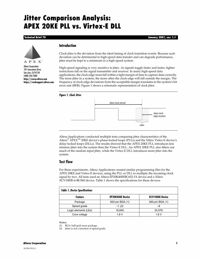
High-speed signaling is very sensitive to jitter. As signals toggle faster and faster, tighter restrictions fall on the signal transmitter and receiver. In many high-speed data applications, the clock edge must fall within a tight margin of time to capture data correctly. The more jitter in a system, the more often the clock edge will fall outside the margin. The frequency of clock edge deviations from the acceptable margin translates to the system’s bit error rate (BER). Figure 1 shows a schematic representation of clock jitter.
Figure 1. Clock Jitter
Altera Applications conducted multiple tests comparing jitter characteristics of the Altera® APEXTM 20KE device’s phase-locked loops (PLLs) and the Xilinx Virtex-E device’sdelay-locked loops (DLLs). The results showed that the APEX 20KE PLL introduces less intrinsic jitter into the system than the Virtex-E DLL. An APEX 20KE PLL also filters out much of the random input jitter, while the Virtex-E DLL introduces more jitter into the system.
Test Flow
For these experiments, Altera Applications created similar programming files for the APEX 20KE and Virtex-E devices, using the PLL or DLL to multiply the incoming clock signal by two. All tests used an Altera EP20K400EBC652-1X device and a Xilinx XCV1000E-6-BG560 device. Table 1 shows the specifications for these devices.
Notes:(1) BGA: ball-grid array package.(2) Jitter is not a function of speed grade.
Table 1. Device Specifications
Feature EP20K400E Device XCV1000E Device
Package 652-pin BGA (1) 560-pin BGA (1)
Speed grade –1 (2) –6
Logic elements (LEs) 16,640 24,576
Core voltage 1.8 V 1.8 V
Ideal clock period
Jitter
Ideal clockedge location
Altera Corporation101 Innovation DriveSan Jose, CA 95134(408) 544-7000http://www.altera.comhttps://websupport.altera.com
M-TB-070-01.1
Altera Corporation 1
TB 70: Jitter Comparison Analysis: APEX 20KE vs. Virtex-E Devices
Lab Equipment
Altera used the following equipment in the APEX 20KE and Virtex-E device tests:
� LeCroy LC584AL 1-GHz scope� HP E3614A power supply� HP E4433B signal generator� HP 8133A pulse generator� HP function/arbitrary waveform generator
Test Conditions
Altera used the following test conditions in the APEX 20KE and Virtex-E device tests:
� Core voltage (VCCINT) = 1.8 V� I/O voltage (VCCIO) = 3.3 V� Temperature = room temperature
Intrinsic Jitter Test
Intrinsic jitter is the jitter created by the device itself. To test intrinsic jitter, Altera Applications configured APEX 20KE and Virtex-E devices with PLLs or DLLs in 2× mode. A 50-MHz low-jitter clock was applied to the clock input of the devices, and the output jitter was measured on each device’s external clock output pin. The “period at level” feature of the LC584AL scope measured the period of the input waveform over a number of sweeps. After the voltage level was selected, the scope measured the time between successive positive edge crossings of that voltage level to determine the period of the waveform. The scope recorded a period for every sweep and calculated the sigma from the distribution of all measured periods. This sigma was equivalent to the root mean square (RMS) period jitter of the waveform. For this experiment, a large number of sweeps were taken until the sigma value visually stabilized on the scope. All measurements were done under quiet conditions.
2 Altera Corporation
TB 70: Jitter Comparison Analysis: APEX 20KE vs. Virtex-E Devices
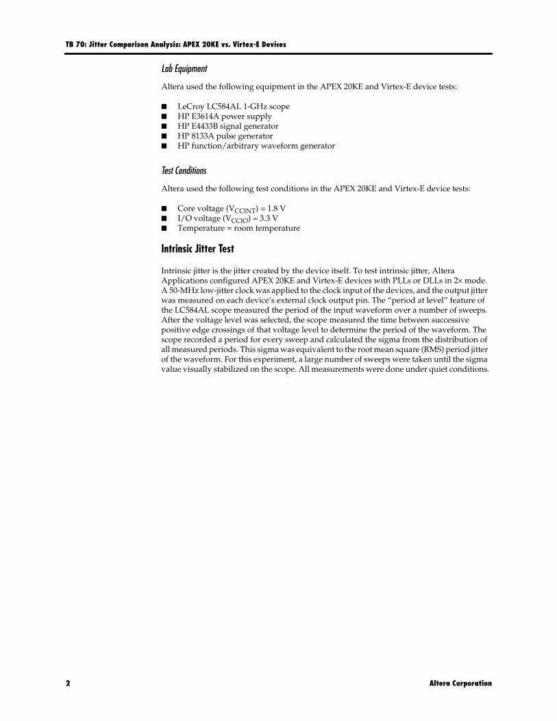
Figure 2 shows the input clock jitter distribution of the 50-MHz clock signal. In Figure 2, the RMS period jitter of the waveform that was driven to both devices was approximately 4 ps.
Figure 2. Input Clock Jitter Distribution (50 MHz)
Altera Corporation 3
TB 70: Jitter Comparison Analysis: APEX 20KE vs. Virtex-E Devices
APEX 20KE Jitter Distribution
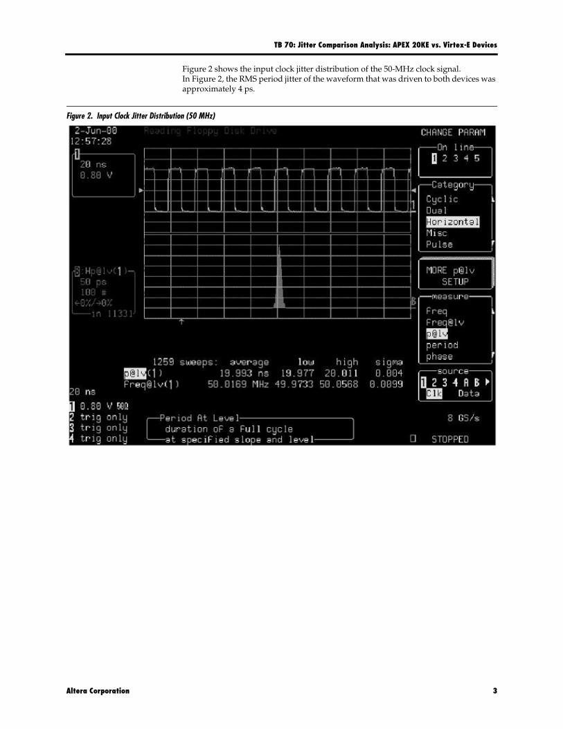
Figure 3 shows output jitter distribution of an APEX 20KE device output when the50-MHz signal (shown in Figure 2) is driven into the APEX PLL. The output jitter distribution of the APEX 20KE device has a sigma value of 15 ps with a 2× frequency average of 100.005 MHz. The jitter distribution curve peak is centered on the ideal period. Using a 6× sigma as the value for peak-to-peak jitter, the maximum peak-to-peak jitter is 90 ps.
Figure 3. APEX 20KE PLL Output Jitter Distribution (2× mode)
90 ps
4 Altera Corporation
TB 70: Jitter Comparison Analysis: APEX 20KE vs. Virtex-E Devices
Virtex-E DLL Output Jitter Distribution
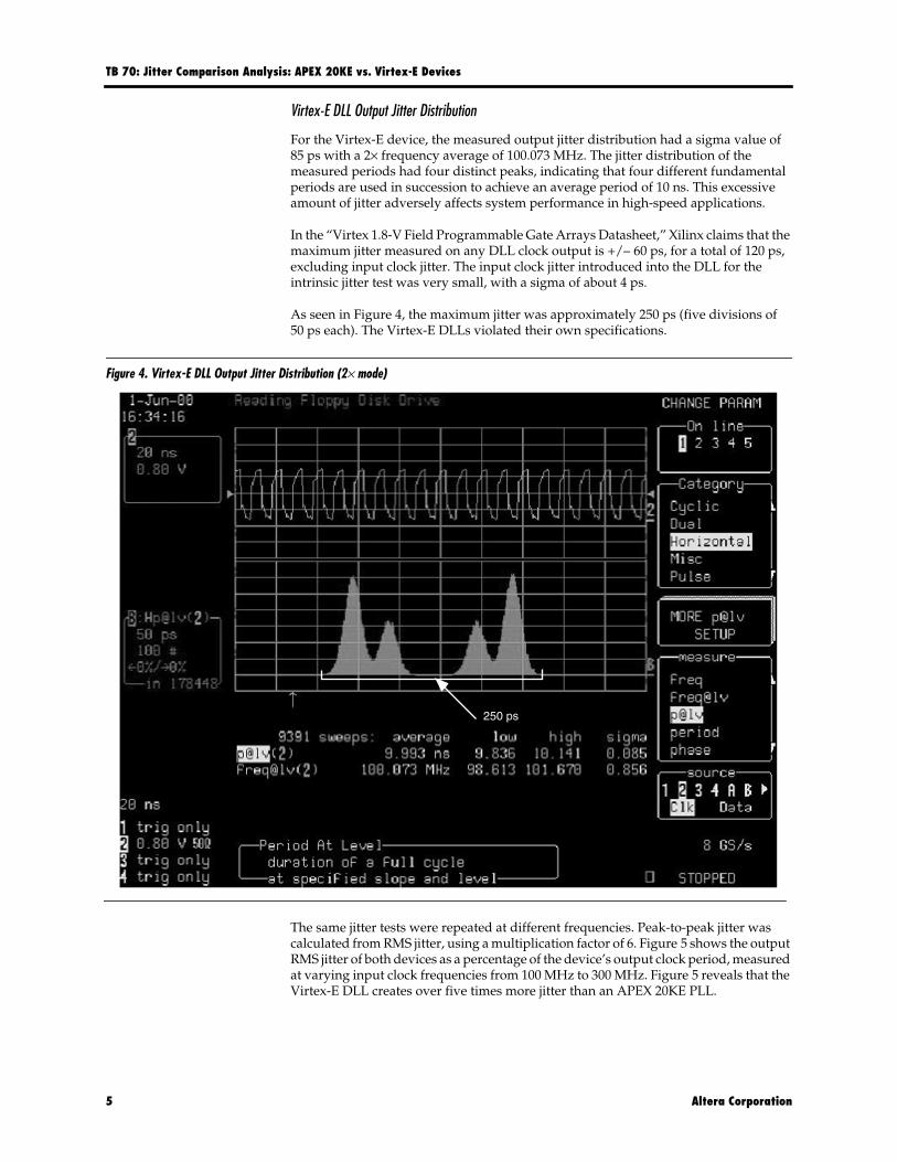
For the Virtex-E device, the measured output jitter distribution had a sigma value of 85 ps with a 2× frequency average of 100.073 MHz. The jitter distribution of the measured periods had four distinct peaks, indicating that four different fundamental periods are used in succession to achieve an average period of 10 ns. This excessive amount of jitter adversely affects system performance in high-speed applications.
In the “Virtex 1.8-V Field Programmable Gate Arrays Datasheet,” Xilinx claims that the maximum jitter measured on any DLL clock output is +/– 60 ps, for a total of 120 ps, excluding input clock jitter. The input clock jitter introduced into the DLL for the intrinsic jitter test was very small, with a sigma of about 4 ps.
As seen in Figure 4, the maximum jitter was approximately 250 ps (five divisions of 50 ps each). The Virtex-E DLLs violated their own specifications.
Figure 4. Virtex-E DLL Output Jitter Distribution (2× mode)
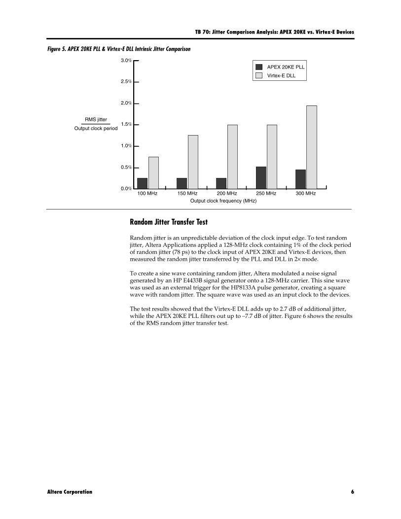
The same jitter tests were repeated at different frequencies. Peak-to-peak jitter was calculated from RMS jitter, using a multiplication factor of 6. Figure 5 shows the output RMS jitter of both devices as a percentage of the device’s output clock period, measured at varying input clock frequencies from 100 MHz to 300 MHz. Figure 5 reveals that the Virtex-E DLL creates over five times more jitter than an APEX 20KE PLL.
250 ps
5 Altera Corporation
TB 70: Jitter Comparison Analysis: APEX 20KE vs. Virtex-E Devices
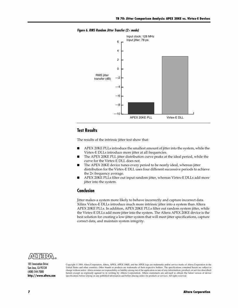
Random jitter is an unpredictable deviation of the clock input edge. To test random jitter, Altera Applications applied a 128-MHz clock containing 1% of the clock period of random jitter (78 ps) to the clock input of APEX 20KE and Virtex-E devices, then measured the random jitter transferred by the PLL and DLL in 2× mode.
To create a sine wave containing random jitter, Altera modulated a noise signal generated by an HP E4433B signal generator onto a 128-MHz carrier. This sine wave was used as an external trigger for the HP8133A pulse generator, creating a square wave with random jitter. The square wave was used as an input clock to the devices.
The test results showed that the Virtex-E DLL adds up to 2.7 dB of additional jitter, while the APEX 20KE PLL filters out up to –7.7 dB of jitter. Figure 6 shows the results of the RMS random jitter transfer test.
Virtex-E DLL
APEX 20KE PLL
0.0%
0.5%
1.0%
1.5%
2.0%
2.5%
3.0%
100 MHz 150 MHz 200 MHz 250 MHz 300 MHz
RMS jitter
Output clock period
Output clock frequency (MHz)
Altera Corporation 6
TB 70: Jitter Comparison Analysis: APEX 20KE vs. Virtex-E Devices
Copyright 2001 Altera Corporation. Altera, APEX, APEX 20KE, and the APEX logo are trademarks and/or service marks of Altera Corporation in theUnited States and other countries. Other brands or products are trademarks of their respective holders. The specifications contained herein are subject tochange without notice. Altera assumes no responsibility or liability arising out of the application or use of any information, product, or service describedherein except as expressly agreed to in writing by Altera Corporation. Altera customers are advised to obtain the latest version of devicespecifications before relying on any published information and before placing orders for products or services. All rights reserved.
®
101 Innovation DriveSan Jose, CA 95134(408) 544-7000http://www.altera.com
Figure 6. RMS Random Jitter Transfer (2× mode)
Test Results
The results of the intrinsic jitter test show that:
� APEX 20KE PLLs introduce the smallest amount of jitter into the system, while the Virtex-E DLLs introduce more jitter at all frequencies.
� The APEX 20KE PLL jitter distribution curve peaks at the ideal period, while the curve for the Virtex-E DLL does not.
� The APEX 20KE device tunes every period to be nearly ideal, whereas jitter distribution for the Virtex-E DLL uses four different successive periods to achieve the 2× frequency average.
� APEX 20KE PLLs filter out input random jitter, whereas Virtex-E DLLs add more jitter into the system.
Conclusion
Jitter makes a system more likely to behave incorrectly and capture incorrect data. Xilinx Virtex-E DLLs introduce much more intrinsic jitter into a system than Altera APEX 20KE PLLs. In addition, APEX 20KE PLLs filter out random system jitter, while the Virtex-E DLLs add more jitter into the system. The Altera APEX 20KE device is the best solution for creating a low-jitter system that will meet jitter specifications, capture correct data, and maintain system integrity.


![20ke coo, K Mg 20kg CORP., K Mg * BB] COARSE 20ke N Mg Mg ...](https://static.documents.pub/doc/80x56/61ca9e8471c5141a2f3b4c43/20ke-coo-k-mg-20kg-corp-k-mg-bb-coarse-20ke-n-mg-mg-.jpg)


