1. General description The TDA8026 is a cost-effective, analog interface for addressing multiple smart card slots in a Point Of Sales (POS) terminal. It can address up to two main cards (synchronous or asynchronous smart cards supported) and up to four Security Access Modules (SAMs). Its packaging supports the latest payment terminal security requirements. 2. Features and benefits I 2 C-bus controlled IC card interface in a TFBGA64 package Supply voltage between 2.7 V and 5.5 V Dedicated microcontroller interface supply voltage (V DD(INTF) ) Shutdown mode ensures very low power consumption when the TDA8026 is inactive Programmable power reduction modes triggered when the card slots are inactive V CC(n) generation via DC-to-DC converter: two card slots can be fully loaded, the three others in reduced consumption mode Two clock input pins: CLKIN1 for card slot 1 and CLKIN2 for card slots 2 to 5 Two transparent I/O lines on microcontroller side, one for card slot 1 and the other for card slots 2 to 5 Five protected, half-duplex, bidirectional, buffered I/O lines with current limitation at 15 mA and a maximum frequency 1 MHz Two I 2 C-bus controlled auxiliary I/O lines V CC(n) regulation on all card slots at I CC 55 mA: 5 V, 3 V or 1.8 V 5 % Current spikes of 40 nAs up to 20 MHz for 5 V cards with controlled rise and fall times Current limitation of approximately 100 mA Thermal protection and short-circuit protection on all card contacts Automatic activation and deactivation sequences initiated by the software or hardware in the event of a short-circuit, card take-off or voltage drop-out for V DD(INTF) , V DD or V UP Enhanced ElectroStatic Discharge (ESD) protection on the card-side up to 6 kV 20 MHz clock input Card clock generation up to 20 MHz and dividable by 1, 2, 4 or 5 with synchronous frequency changes: Stop, HIGH or LOW Clock frequency between 1 MHz and 2.2 MHz in card low-power mode Current limitation on pin CLK (n) TDA8026 Multiple smart card slot interface IC Rev. 1.1 — 30 June 2016 Product data sheet
Transcript
1. General description
The TDA8026 is a cost-effective, analog interface for addressing multiple smart card slots in a Point Of Sales (POS) terminal. It can address up to two main cards (synchronous or asynchronous smart cards supported) and up to four Security Access Modules (SAMs). Its packaging supports the latest payment terminal security requirements.
2. Features and benefits
I2C-bus controlled IC card interface in a TFBGA64 package
Supply voltage between 2.7 V and 5.5 V
Dedicated microcontroller interface supply voltage (VDD(INTF))
Shutdown mode ensures very low power consumption when the TDA8026 is inactive
Programmable power reduction modes triggered when the card slots are inactive
VCC(n) generation via DC-to-DC converter: two card slots can be fully loaded, the three others in reduced consumption mode
Two clock input pins: CLKIN1 for card slot 1 and CLKIN2 for card slots 2 to 5
Two transparent I/O lines on microcontroller side, one for card slot 1 and the other for card slots 2 to 5
Five protected, half-duplex, bidirectional, buffered I/O lines with current limitation at 15 mA and a maximum frequency 1 MHz
Two I2C-bus controlled auxiliary I/O lines
VCC(n) regulation on all card slots at ICC 55 mA:
5 V, 3 V or 1.8 V 5 %
Current spikes of 40 nAs up to 20 MHz for 5 V cards with controlled rise and fall times
Current limitation of approximately 100 mA
Thermal protection and short-circuit protection on all card contacts
Automatic activation and deactivation sequences initiated by the software or hardware in the event of a short-circuit, card take-off or voltage drop-out for VDD(INTF), VDD or VUP
Enhanced ElectroStatic Discharge (ESD) protection on the card-side up to 6 kV
20 MHz clock input
Card clock generation up to 20 MHz and dividable by 1, 2, 4 or 5 with synchronous frequency changes:
Stop, HIGH or LOW
Clock frequency between 1 MHz and 2.2 MHz in card low-power mode
Current limitation on pin CLK(n)
TDA8026Multiple smart card slot interface ICRev. 1.1 — 30 June 2016 Product data sheet
NXP Semiconductors TDA8026Multiple smart card slot interface IC
RST(n) signal lines with current limitation at 20 mA, controlled by an embedded programmable clock pulse counter on asynchronous cards or by a register on synchronous cards
ISO 7816-3 and EMV 4.31 payment systems compatibility
VDD(INTF) supply voltage supervisor ensures correct communication between microcontroller and circuit; threshold internally fixed or set using an external resistor bridge
VDD supply voltage supervisor for spike suppression during power-on and emergency deactivation at power-off; threshold internally fixed
Card presence input with a 17.8 ms (typical) built-in debouncing system on card slots 1 and 2
One interrupt signal (IRQN)
3. Applications
Point Of Sale terminals
Multiple SAM contact readers
4. Quick reference data
1. for C3 version
Table 1. Quick reference data VDD = VDD(INTF) = 3.3 V; fclk(ext) = 10 MHz; GND = 0 V; inductor = 10 H; decoupling capacitors on pins VDD and VUP = 10 F; Tamb = 25 C unless otherwise specified.
Symbol Parameter Conditions Min Typ Max Unit
Supply
VDD supply voltage on pin VDD; DC-to-DC converter on [1] 2.7 - 5.5 V
on pin VDD; DC-to-DC converter off and VCC(n) pin = 5 V
[1] 5.25 - 5.5 V
IDD supply current shutdown mode - 25 40 A
Standby mode - 300 450 A
clock-stop mode; all card slots in this mode; fclk(ext) stopped on pins CLK(n); pins CLKIN1 and CLKIN2 either stopped, HIGH-level or LOW-level
- 3.7 - mA
active mode; all VCC(n) pins = 5 V; fclk(ext) on pins CLK(n) = 5 MHz; ICC(1) = ICC(2) = 55 mA; ICC(3) = ICC(4) = ICC(5) = 2 mA
[2] [3]
- 210 260 mA
VDD(INTF) interface supply voltage on pin VDD(INTF) 1.6 - 3.6 V
IDD(INTF) interface supply current shutdown mode - 10 15 A
active mode; all VCC(n) pins = 5 V; fclk(ext) on pins CLK(n) = 5 MHz
Product data sheet Rev. 1.1 — 30 June 2016 2 of 61
NXP Semiconductors TDA8026Multiple smart card slot interface IC
[1] Refer to Section 8.6 for further information about the DC-to-DC converter operation.
[2] Typical value measurement based on a 85 % DC-to-DC converter and inductance efficiency; depends on PCB layout and external component quality (inductor, capacitor).
[3] Maximum value measurement based on a 125 mA (sum of all card supply currents on pins VCC(n)) current load and a 75 % DC-to-DC converter and inductance efficiency; depends on PCB layout and external component quality (inductor, capacitor).
[4] Two ceramic multilayer 100 nF (minimum) capacitors with a low Equivalent Series Resistance (ESR) should be used to meet these specifications.
[5] Output voltage to the card including ripple.
[6] Refer to Section 8.8.3 for further information.
Card supply voltage pins: VCC(1) to VCC(5)[4]
VCC supply voltage active mode; 2.7 V < VDD < 5.5 V [5]
5 V card; DC ICC(n) 55 mA 4.75 5 5.25 V
3 V card; DC ICC(n) 55 mA 2.85 3 3.15 V
1.8 V card; DC ICC(n) 35 mA 1.71 1.8 1.89 V
active mode; AC current pulses with I < 200 mA, t < 400 ns and f < 20 MHz
[5]
5 V card; current spikes of 40 nAs 4.65 - 5.35 V
3 V card; current spikes of 17.5 nAs 2.76 - 3.24 V
1.8 V card; current spikes of 11.1 nAs 1.62 - 1.98 V
Vripple(p-p) peak-to-peak ripple voltage
20 kHz to 200 MHz with default Register6 (Slew Rate register) settings
- - 350 mV
ICC supply current VCC(n) = 5 V - - 55 mA
VCC(n) = 3 V - - 55 mA
VCC(n) = 1.8 V - - 35 mA
sum of all card supply currents on pins VCC(n); active mode; All VCC pins = 5 V; fclk(ext) on pins CLK(n) = 5 MHz; ICC(1) = ICC(2) = 55 mA; ICC(3) = ICC(4) = ICC(5) = 2 mA
[3] - 116 125 mA
General
tdeact deactivation time total sequence [6] 60 80 100 s
tdeb debounce time - 17.8 23.8 ms
Ptot total power dissipation Tamb = 25 C to +85 C - 455 665 mW
Tamb ambient temperature 25 +25 +85 C
Table 1. Quick reference data …continuedVDD = VDD(INTF) = 3.3 V; fclk(ext) = 10 MHz; GND = 0 V; inductor = 10 H; decoupling capacitors on pins VDD and VUP = 10 F; Tamb = 25 C unless otherwise specified.
Product data sheet Rev. 1.1 — 30 June 2016 8 of 61
NXP Semiconductors TDA8026Multiple smart card slot interface IC
8. Functional description
Remark: Throughout this document ISO 7816-3 and EMV standard terminology conventions have been adhered to and it is assumed that the reader is familiar with these.
8.1 Power supplies
The TDA8026 supply pins are VDD, VDD(INTF) and GND1 to GND10.
• VDD must be between 2.7 V and 5.5 V
• VDD(INTF) must be between 1.6 V and 3.6 V
The VDD, VDD(INTF) supply voltages can be applied to the device at any time, in any sequence. All interface signals to the system controller are referenced to the VDD(INTF) supply voltage which can be lower or higher than VDD. The integrated DC-to-DC converter generates the card supply voltage (VCC(n)) of either 5 V , 3 V or 1.8 V ( 5 %). In addition, the internal voltage regulator delivers VDD(INTREGD) 3.3 V supply voltage.
8.2 Power modes
Three power modes are available for the TDA8026. These are:
• Standby mode
• Active mode with a clock-stop sub-mode
• Shutdown mode
(1) Active mode; DC-to-DC converter is ON.
(2) VCC(n) overcurrent on a card slot causes deactivation of a faulty card slot. All others remain active.
Product data sheet Rev. 1.1 — 30 June 2016 9 of 61
NXP Semiconductors TDA8026Multiple smart card slot interface IC
8.2.1 Standby mode
In Standby mode, both the supply voltages VDD and VDD(INTF) are applied within the specification limits as described in Table 40 on page 40. In addition, the DC-to-DC converter is not running and the card slots are not activated.
8.2.2 Active mode
In active mode, both the VDD and VDD(INTF) supply voltages are applied to the device within the specification limits as described in Table 40 on page 40. A minimum of one card slot is activated. All card slots can be activated at once and communication performed with up to two cards slots.
The DC-to-DC converter has been developed to handle a 116 mA (typical) DC load. This allows two active card slots to communicate with a load of 55 mA while the three remaining card slots are in clock-stop mode (see Section 8.2.3 for information about this mode) with a 2 mA load.
The DC-to-DC converter overload protection is triggered when a higher current load than specified in Table 40 on page 40 is supplied to the DC-to-DC converter (see Section 8.11 for further information).
8.2.3 Clock-stop mode
Clock-stop mode is a low-power mode which is triggered when a card is activated without any communication. In this mode, a supply voltage with a low frequency clock is applied to cards that do not support the clock-stop feature.
8.2.4 Shutdown mode
Shutdown mode is the very low power consumption mode, typically 25 A. The TDA8026 enters this mode when the SDWNN pin is driven LOW. Only presence monitoring on card slot 1 remains enabled. When card insertion or removal is detected on card slot 1, an interrupt signal (IRQN) is sent to the microcontroller.
In shutdown mode, it is assumed that the VDD(INTF) and VDD supply voltages are stable and the SDWNN pin is active LOW.
8.2.4.1 Entering shutdown mode
Shutdown mode is activated when the SDWNN pin is driven LOW. On entering this mode:
1. All card slots are automatically deactivated
2. The power consumption is reduced on completion of the deactivation sequence.
This causes the following:
• Digital module moves in to reset mode. However, card presence monitoring on slot 1 continues to operate normally
• All card slots are disabled and all card pins are forced to 0 V. Again, card presence monitoring on slot 1 continues to operate normally
• Thermal protection is disabled
• The DC-to-DC converter is bypassed
• All interface signal pull-up resistors are disconnected from their supply rail (except the pull-up resistor on the SDWNN pin)
Product data sheet Rev. 1.1 — 30 June 2016 11 of 61
NXP Semiconductors TDA8026Multiple smart card slot interface IC
8.3 Voltage supervisors
8.3.1 Block diagram
8.3.2 Description
The voltage supervisor can be used to perform Power-On Resets (POR) and supply drop detection during a card session. The supervisors control the internal regulated supply voltage (VDD(INTREGD)) and the microcontroller interface supply voltage (VDD(INTF)) to ensure problem-free operation of the TDA8026. This block controls:
• VDD using the internal voltage regulator’s output (VDD(INTREGD))
• the microcontroller interface supply voltage (VDD(INTF)) using the voltage on the PORADJ pin (VPORADJ)
When an alarm occurs, the internal digital controller resets the TDA8026.
Product data sheet Rev. 1.1 — 30 June 2016 13 of 61
NXP Semiconductors TDA8026Multiple smart card slot interface IC
8.4 I2C-bus description
Remark: Refer to the I2C-bus specification for more information.
The I2C-bus interface in the TDA8026 is an I2C-bus slave operating either Standard mode (100 kHz) or Fast mode (400 kHz). In addition, it integrates shift register functions, shift timing generation and slave address recognition.
8.4.1 I2C-bus protocol
The I2C-bus protocol is based on bidirectional, 2-line communication between ICs or modules. The serial bus consists of two bidirectional lines: one for data signals (SDA) and one for clock signals (SCL). Both the SDA and SCL lines must be connected to the VDD(INTF) supply voltage using a pull-up resistor (refer to the I2C-bus specification for more details).
The I2C-bus protocol is defined as follows:
• Data transfer can only be initialized when the I2C-bus is not busy.
• During data transfer, the data line must remain stable when the clock line is HIGH. Changes in the data line while the clock line is HIGH are interpreted as control signals.
8.4.2 Bus conditions
The following bus conditions are defined.
Bus not busy — Both data and clock lines remain HIGH.
Start data transfer — The START condition is generated when the state of the data line changes from HIGH to LOW while the clock line is HIGH.
Stop data transfer — The STOP condition is generated when the state of the data line changes from LOW to HIGH while the clock line is HIGH.
Data valid — The data line state represents valid data, after a START condition with the data line stable for the duration of the clock signal HIGH period. There is one clock pulse per bit of data.
8.4.3 Data transfer
Each data transfer is triggered by a START condition and finished by a STOP condition (see Figure 13 for timing information).
Data transfers can be performed in Standard mode at 100 kHz or Fast mode at 400 kHz. Data transfer is performed on a byte for byte basis in both read or write modes. The information is transmitted in bytes and each receiver acknowledges with a 9th bit (acknowledge).
Each byte is followed by an acknowledge bit and the transmitter must release the SDA line during the acknowledge bit. The master generates an extra acknowledge related clock pulse. The addressed slave receiver must generate an acknowledge bit after receiving each byte. The master-receiver must generate an acknowledge bit after receiving each byte clocked out of the slave transmitter.
The acknowledging device must pull-down the SDA line during the acknowledge clock pulse to ensure the SDA line is stable LOW during the acknowledge related clock pulse HIGH period.
Product data sheet Rev. 1.1 — 30 June 2016 14 of 61
NXP Semiconductors TDA8026Multiple smart card slot interface IC
In addition, the set-up and hold times must be taken into account. The master-receiver must signal the end of the last data byte to the slave transmitter by not sending an acknowledge bit on the last byte that has been clocked out of the slave. The transmitter must ensure the data line is HIGH to enable the master to generate the STOP condition.
8.4.4 Device addressing
Three device addresses are needed to control the TDA8026.
• One high address: The high address enables selection of a bank page (Bank 0 or Bank 1) based on a configuration byte. A bank page relates to a card slot or general registers. See Table 7 for detailed information.
• Two low addresses: The microcontroller uses two low addresses to read and write into the selected bank page (see Table 6 on page 15 to Table 39 on page 38 for detailed information).
The addresses for the device are shown in Table 5 and Table 6.
Bit 1 is the address bit which selects Register0 or Register1. Bit 0 defines either Read or Write mode.
• When bit 0 is set to logic 1, read mode is selected
• When bit 0 is set to logic 0, write mode is selected
Bank 1 page selection is performed when the configuration byte (CSb[7:0]) is written to the high address representing bank 0 based on the A0 pin value.
Using pin A0, two TDA8026s can be used in parallel based on the selection made to the address selection pin A0. Pin A0 is externally hardwired to the pins VDD(INTF) or GND. The voltage on the A0 pin sets the bit 2 address bit
Product data sheet Rev. 1.1 — 30 June 2016 15 of 61
NXP Semiconductors TDA8026Multiple smart card slot interface IC
8.5 Banks and registers
The device registers enable the microcontroller to control the TDA8026. These registers are defined as banks:
• Bank 0 register is a read/write register which enables selection of the required card slot number and access to the corresponding registers Bank 1 registers. In addition, Bank 0 is used to write information about the interrupt status and the product version. The registers in bank 0 (CSb[7:0] = 1h to 5h) are similar to the registers of the TDA8023.
• Bank 1 provides access to the corresponding card slot registers. Bank 1 is composed of several pages which in turn contain registers related to each individual card slot or general registers. Typically, pages can contain two general registers or five card slot related registers.
Remark: The registers are organized in bank pages in order to keep compatibility with the TDA8023.
Bank 1 page selection is performed when the configuration byte (CSb[7:0]) is written to the high I2C-bus address representing bank 0 based on the A0 pin.
Product data sheet Rev. 1.1 — 30 June 2016 16 of 61
xxxxxxxxxxxxxxxxxxxxx xxxxxxxxxxxxxxxxxxxxxxxxxx xxxxxxx x x x xxxxxxxxxxxxxxxxxxxxxxxxxxxxxx xxxxxxxxxxxxxxxxxxx xx xx xxxxx xxxxxxxxxxxxxxxxxxxxxxxxxxx xxxxxxxxxxxxxxxxxxx xxxxxx xxxxxxxxxxxxxxxxxxxxxxxxxxxxxxxxxxx xxxxxxxxxxxx x x xxxxxxxxxxxxxxxxxxxxx xxxxxxxxxxxxxxxxxxxxxxxxxxxxxx xxxxx xxxxxxxxxxxxxxxxxxxxxxxxxxxxxxxxxxxxxxxxxxxxxxxxxx xxxxxxxx xxxxxxxxxxxxxxxxxxxxxxxxx xxxxxxxxxxxxxxxxxxxx xxx
TD
A80
26_1
Pro
du
ct data sh
NX
P S
emico
nd
ucto
rsT
DA
8026M
ultip
le s
ma
rt ca
rd s
lot in
terfac
e IC
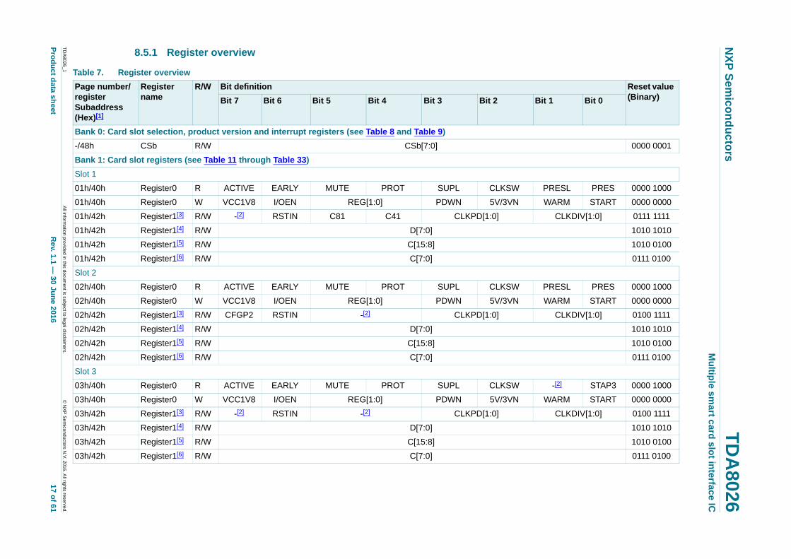
8.5.1 Register overview
Table 7. Register overview
Page number/register
Register name
R/W Bit definition Reset value (Binary)Bit 1 Bit 0
xxxxxxxxxxxxxxxxxxxxx xxxxxxxxxxxxxxxxxxxxxxxxxx xxxxxxx x x x xxxxxxxxxxxxxxxxxxxxxxxxxxxxxx xxxxxxxxxxxxxxxxxxx xx xx xxxxx xxxxxxxxxxxxxxxxxxxxxxxxxxx xxxxxxxxxxxxxxxxxxx xxxxxx xxxxxxxxxxxxxxxxxxxxxxxxxxxxxxxxxxx xxxxxxxxxxxx x x xxxxxxxxxxxxxxxxxxxxx xxxxxxxxxxxxxxxxxxxxxxxxxxxxxx xxxxx xxxxxxxxxxxxxxxxxxxxxxxxxxxxxxxxxxxxxxxxxxxxxxxxxx xxxxxxxx xxxxxxxxxxxxxxxxxxxxxxxxx xxxxxxxxxxxxxxxxxxxx xxx
TD
A80
26_1
Pro
du
ct data sh
NX
P S
emico
nd
ucto
rsT
DA
8026M
ultip
le s
ma
rt ca
rd s
lot in
terfac
e IC
-[2] STAP4 0000 1000
WARM START 0000 0000
CLKDIV[1:0] 0100 1111
1010 1010
1010 0100
0111 0100
-[2] STAP5 0000 1000
WARM START 0000 0000
CLKDIV[1:0] 0100 1111
1010 1010
1010 0100
0111 0100
1100 0010
0001 1111
IO_SR[1:0] 0100 0100
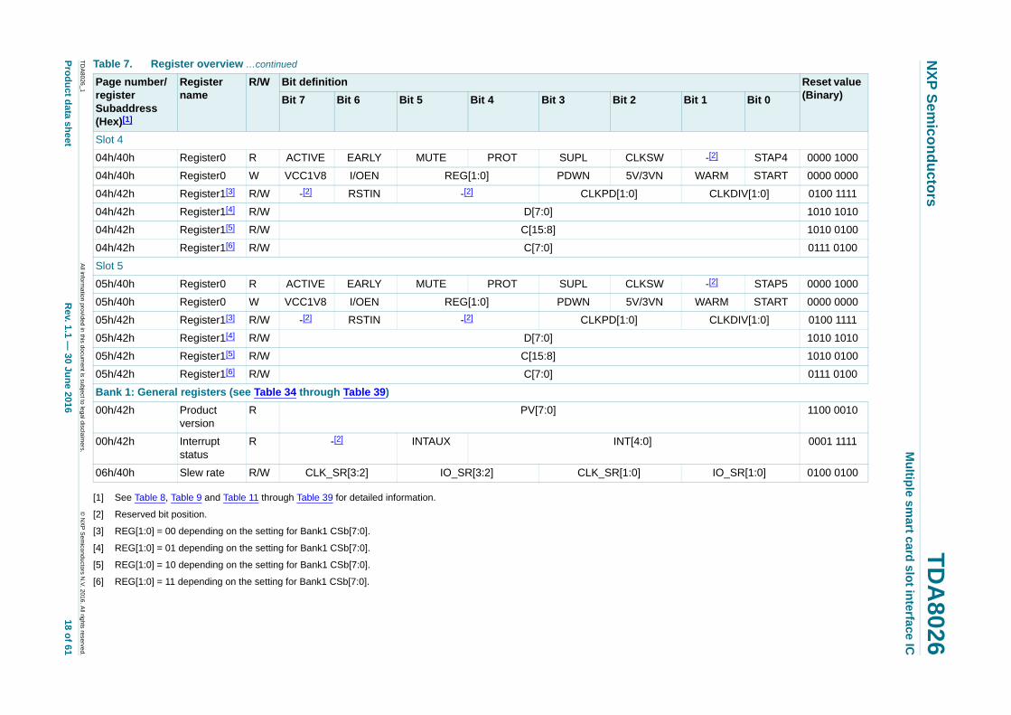
Table 7. Register overview …continued
Page number/register Subaddress (Hex)[1]
Register name
R/W Bit definition Reset value (Binary)Bit 7 Bit 6 Bit 5 Bit 4 Bit 3 Bit 2 Bit 1 Bit 0
NXP Semiconductors TDA8026Multiple smart card slot interface IC
8.5.2 Bank 0 register description
The device registers enable the microcontroller to control the TDA8026. The registers are organized in bank pages to ensure compatibility with the TDA8023.
Bank 0 write register enables selection of the card slot number and access to the corresponding registers in bank 1. The card slot registers in bank 1 are accessed using the configuration byte (CSb[7:0]). The range 01h to 05h is used to select the specific card slot starting at card slot 1 (01h) and ending with card slot 5 (05h) in a similar way to the TDA8023 registers.
8.5.2.1 Bank 0 register (address: 48h) bit allocation
8.5.2.2 Bank 0 bit description
8.5.3 Bank 1 card slots 1 and 2 register descriptions
8.5.3.1 Bank 1 CSb[7:0] Register0 (address 40h) card slot 1 and card slot 2 bit allocation
[1] See Table 11 for the read mode bits and Table 12 for the write mode bits.
When at least one of the PRESL, SUPL, PROT, MUTE and EARLY bits is set to logic 1, IRQN pin is driven LOW until the status byte has been read. After power-on, the SUPL bit is set to logic 1 until the status byte has been read and the IRQN pin is LOW until the voltage supervisor is deactivated.
Table 8. Bank 0 register (address: 48h) bit allocation
Bit 7 6 5 4 3 2 1 0
Symbol CSb[7:0]
Access R/W
Table 9. Bank 0 bit description
Bit Symbol Value Description
7 to 0 CSb[7:0] Bank 1 page selection:
00h selects product version and interrupts status register page
01h selects card slot 1 page
02h selects card slot 2 page
03h selects card slot 3 page
04h selects card slot 4 page
05h selects card slot 5 page
06h selects the clock frequency and I/O lines slew rate settings page
Table 10. Bank 1 CSb[7:0] Register0 (address 40h) card slot 1 and card slot 2 bit allocation
Product data sheet Rev. 1.1 — 30 June 2016 20 of 61
NXP Semiconductors TDA8026Multiple smart card slot interface IC
8.5.3.3 Bank 1 Register0 card slot 1 (address 01h) and card slot 2 (address 02h) write mode bit descriptions
[1] This bit cannot be written when the START bit is logic 1.
[2] It is a mandatory condition for card slots 2 to 5 that only one card slot I/O line is enabled at a time. When switching from one slot to another, the enabled I/O must be disabled before the I/O line for the required card slot is enabled.
Remark: If both pins I/OUC1 and I/OUC2 are connected at the same time, this mandatory condition also applies to card slot 1.
[3] In synchronous mode, this bit cannot be written when START bit is logic 1.
Table 12. Bank 1 Register0 card slot 1 (address 01h) and card slot 2 (address 02h) write mode bit descriptions
Bit Symbol Value Description
7 VCC1V8[1] used together with the 5V/3VN bit
1 set to logic 1: VCC(n) = 1.8 V; ignores the 5V/3VN bit logic state
0 set to logic 0: VCC(n) is set using the 5V/3VN bit
6 I/OEN[2] 1 set to logic 1: pins I/OUCn are switched to pins I/O(n)
0 set to logic 0: pins I/OUCn and I/O(n) are high-impedance with internal pull-up resistor
5 to 4 REG[1:0] - See Table 13 “Bank 1 CSb[7:0] Register0 (address 42h) card slots 1 and card slots 2 bit allocation” on page 22 for detailed information
3 PWDN[3] 1 set to logic 1 to apply the CLKPD[1:0] bit clock settings to pin CLK(n) for the selected card slot
0 set to logic 0 to apply the CLKDIV[1:0] bits clock options to pin CLK(n) for the selected card slot
2 5V/3VN[1] 1 used together with VCC1V8 bit.
set to logic 1 and the VCC1V8 bit is logic 0: VCC(n) = 5 V
0 set to logic 0 and the VCC1V8 bit is logic 0: VCC(n) = 3 V
1 WARM 1 set to logic 1: a warm reset procedure is started
0 set to logic 0: by hardware when a START bit is detected or when MUTE bit is set to logic 1
0 START 1 set to logic 1: starts the activation sequence and cold reset procedure (only if the SUPL and PROT bits are logic 0 and the PRES bit is logic 1)
0 set to logic 0: starts the deactivation sequence
Card Slot 1 Reg[1:0] = 00; see Table 14 on page 22
Symbol -[1] RSTIN C8(1) C4(1) CLKPD[1:0][2] CLKDIV[1:0][3]
Access R/W R/W R/W R/W R/W R/W R/W R/W
Card Slot 2 Reg[1:0] = 00; see Table 14 on page 22
Symbol CFGP2 RSTIN -[1] CLKPD[1:0][2] CLKDIV[1:0[3]]
Access R/W R/W R/W R/W R/W R/W R/W R/W
Card Slot 1 and card slot 2 Reg[1:0] = 01; see Table 16 on page 24
Symbol D[7:0]
Access R/W
Card Slot 1 and card slot 2 Reg[1:0] = 10; see Table 18 on page 24
Symbol C[15:8]
Access R/W
Card Slot 1 and card slot 2 Reg[1:0] = 11; see Table 20 on page 24
Symbol C[7:0]
Access R/W
Table 14. Bank 1 Register1 (REG[1:0] = 00) card slot 1 (address 01h) and card slot 2 (address 02h) Read/Write mode bit descriptions
Bit Symbol Value Description
7 CFGP2[1] enables another type of card detection switch to be used on card socket 1 and card socket 2
1 if CFGP2 is logic 1, an interrupt is generated during each power-up because the reset value of CFGP2 is logic level 0. Refer to the Application note AN10724 for further information
0 the reset value of CFGP2 is logic 0. Refer to the Application note AN10724 for further information
6 RSTIN 1 synchronous mode: when set to logic 1, pin RST(n) is set to HIGH
asynchronous mode: RSTIN is controlled by hardware (ATR management)
0 set to logic 0: pin RST(n) is LOW
5 C8(1)[2] - writing C8(1) bit writes the corresponding value on C8(1) pin
- reading C8(1) bit reads the state of C8(1) pin
4 C4(1)[2] - writing C41 bit writes the corresponding value on C4(1) pin
Product data sheet Rev. 1.1 — 30 June 2016 22 of 61
NXP Semiconductors TDA8026Multiple smart card slot interface IC
[1] Only for card slot 2 register.
[2] Only for card slot 1 register.
[3] fclk(ext) is the external clock frequency applied to pins CLKIN1 and CLKIN2.
8.5.3.6 Bank 1 Register1 (REG[1:0] = 01) card slot 1 (address 01h) and card slot 2 (address 02h) bit allocation
3 to 2 CLKPD[1:0] - asynchronous mode: when PWDN bit is set to logic 1, the CLKPD[1] and CLKPD[2] bits define the card clock
- synchronous mode: when the PWDN bit and the START bit are set to logic 1, the CLKPD[2] bit remains logic 0 and the clock frequency is controlled by the CLKPD[1] bit
00 asynchronous mode: the card clock is stopped and set to logic 0
- synchronous mode: the card clock is set to logic 0
01 asynchronous mode: the card clock is stopped and set to logic 1
- synchronous mode: the card clock is set to logic 1
10 asynchronous mode: the card clock =
Remark: (fosc(int) is the internal oscillator frequency)
11 asynchronous mode: the card clock frequency (f(clk)) is set using the CLKDIV[1:0] bits.
1 to 0 CLKDIV[1:0] asynchronous mode: when the PWDN bit is set to logic 0 the CLKDIV[1:0] bits define the card clock frequency.
synchronous mode: the CLKDIV[1:0] bits are logic 0
00 [3]card slot 1 card clock frequency = fclk(ext) on pin CLK(1)
card slot 2 card clock frequency = fclk(ext) on pin CLK(2)
01 card slot 1 card clock frequency = fclk(ext) / 2 on pin CLK(1)
card slots 2 card clock frequency = fclk(ext) / 2 on pin CLK(2)
10 card slot 1 card clock frequency = fclk(ext) / 4 on pin CLK(1)
card slot 2 card clock frequency = fclk(ext) / 4 on pin CLK(2)
11 card slot 1 card clock frequency = fclk(ext) / 5 on pin CLK(1)
card slot 2 card clock frequency = fclk(ext) / 5 on pin CLK(2)
Table 14. Bank 1 Register1 (REG[1:0] = 00) card slot 1 (address 01h) and card slot 2 (address 02h) Read/Write mode bit descriptions …continued
Bit Symbol Value Description
fosc int 2
Table 15. Bank 1 Register1 (REG[1:0] = 01) card slot 1 (address 01h) and card slot 2 (address 02h) bit allocation
Product data sheet Rev. 1.1 — 30 June 2016 23 of 61
NXP Semiconductors TDA8026Multiple smart card slot interface IC
8.5.3.7 Bank 1 Register1 (REG[1:0] = 01) card slot 1 (address 01h) and card slot 2 (address 02h) read/write mode bit descriptions
8.5.3.8 Bank 1 Register1 (REG[1:0] = 10) card slot 1 (address 01h) and card slot 2 (address 02h) bit allocation
8.5.3.9 Bank 1 Register1 (REG[1:0] = 10) card slot 1 (address 01h) and card slot 2 (address 02h) read/write mode bit descriptions
8.5.3.10 Bank 1 Register1 (REG[1:0] = 11) card slot 1 (address 01h) and card slot 2 (address 02h) bit allocation
8.5.3.11 Bank 1 Register1 (REG[1:0] = 11) card slot 1 (address 01h) and card slot 2 (address 02h) read/write mode bit descriptions
Table 16. Bank 1 Register1 (REG[1:0] = 01) card slot 1 (address 01h) and card slot 2 (address 02h) Read/Write mode bit descriptions
Bit Symbol Description
7 to 0 D[7:0] programmable 8-bit clock counter. This value is applied to all slots. The reset value is AAh. See Section 8.9 “Answer to reset counters” on page 36
Table 17. Bank 1 Register1 (REG[1:0] = 10) card slot 1 (address 01h) and card slot 2 (address 02h) bit allocation
Bit 7 6 5 4 3 2 1 0
Symbol C[15:8]
Access R/W
Table 18. Bank 1 Register1 (REG[1:0] = 10) card slot 1 (address 01h) and card slot 2 (address 02h) Read/Write mode bit descriptions
Bit Symbol Description
7 to 0 C[15:8] most significant byte of a programmable 16-bit clock counter. This value is applied to all slots. The reset value is A4h. See Section 8.9 “Answer to reset counters” on page 36
Table 19. Bank 1 Register1 (REG[1:0] = 11) card slot 1 (address 01h) and card slot 2 (address 02h) bit allocation
Bit 7 6 5 4 3 2 1 0
Symbol C[7:0]
Access R/W
Table 20. Bank 1 Register1 (REG[1:0] = 11) card slot 1 (address 01h) and card slot 2 (address 02h) read/write mode bit descriptions
Bit Symbol Description
7 to 0 C[7:0] least significant byte of a programmable 16-bit clock counter. This value is applied to all slots. The reset value is 74h. See Section 8.9 “Answer to reset counters” on page 36.
Product data sheet Rev. 1.1 — 30 June 2016 24 of 61
NXP Semiconductors TDA8026Multiple smart card slot interface IC
8.5.4 Card slots 3 to 5 register descriptions
8.5.4.1 Bank 1 CSb[7:0] Register0 (address 40h) card slots 3 to 5 bit allocation
[1] Reserved bit position.
[2] See table Table 22 for more detailed information on read mode bits and Table 23 for more detailed information on write mode bits.
8.5.4.2 Bank 1 Register0 card slot 3 (address 03h), card slot 4 (address 04h) and card slot 5 (address 05h) read mode bit descriptions
When at least one of the SUPL, PROT, MUTE and EARLY bits are set to logic 1, the IRQN pin is driven LOW until the status byte has been read. After power-on, the SUPL bit is set to logic 1 until the status byte has been read and the IRQN pin is LOW until the voltage supervisor is deactivated.
Table 21. Bank 1 CSb[7:0] Register0 (address 40h) card slots 3 to 5 bit allocation
Product data sheet Rev. 1.1 — 30 June 2016 25 of 61
NXP Semiconductors TDA8026Multiple smart card slot interface IC
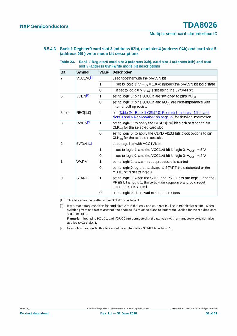
8.5.4.3 Bank 1 Register0 card slot 3 (address 03h), card slot 4 (address 04h) and card slot 5 (address 05h) write mode bit descriptions
[1] This bit cannot be written when START bit is logic 1.
[2] It is a mandatory condition for card slots 2 to 5 that only one card slot I/O line is enabled at a time. When switching from one slot to another, the enabled I/O must be disabled before the I/O line for the required card slot is enabled.
Remark: If both pins I/OUC1 and I/OUC2 are connected at the same time, this mandatory condition also applies to card slot 1.
[3] In synchronous mode, this bit cannot be written when START bit is logic 1.
Table 23. Bank 1 Register0 card slot 3 (address 03h), card slot 4 (address 04h) and card slot 5 (address 05h) write mode bit descriptions
Bit Symbol Value Description
7 VCC1V8[1] used together with the 5V/3VN bit
1 set to logic 1: VCC(n) = 1.8 V; ignores the 5V/3VN bit logic state
0 if set to logic 0 VCC(n) is set using the 5V/3VN bit
6 I/OEN[2] 1 set to logic 1: pins I/OUCn are switched to pins I/O(n)
0 set to logic 0: pins I/OUCn and I/O(n) are high-impedance with internal pull-up resistor
5 to 4 REG[1:0] - see Table 24 “Bank 1 CSb[7:0] Register1 (address 42h) card slots 3 and 5 bit allocation” on page 27 for detailed information
3 PWDN[3] 1 set to logic 1: to apply the CLKPD[1:0] bit clock settings to pin CLK(n) for the selected card slot
0 set to logic 0: to apply the CLKDIV[1:0] bits clock options to pin CLK(n) for the selected card slot
2 5V/3VN[1] used together with VCC1V8 bit
1 set to logic 1: and the VCC1V8 bit is logic 0: VCC(n) = 5 V
0 set to logic 0: and the VCC1V8 bit is logic 0: VCC(n) = 3 V
1 WARM 1 set to logic 1: a warm reset procedure is started
0 set to logic 0: by the hardware: a START bit is detected or the MUTE bit is set to logic 1
0 START 1 set to logic 1: when the SUPL and PROT bits are logic 0 and the PRES bit is logic 1, the activation sequence and cold reset procedure are started
Product data sheet Rev. 1.1 — 30 June 2016 27 of 61
NXP Semiconductors TDA8026Multiple smart card slot interface IC
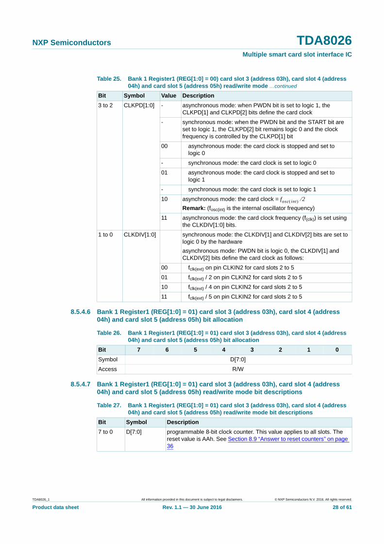
8.5.4.6 Bank 1 Register1 (REG[1:0] = 01) card slot 3 (address 03h), card slot 4 (address 04h) and card slot 5 (address 05h) bit allocation
8.5.4.7 Bank 1 Register1 (REG[1:0] = 01) card slot 3 (address 03h), card slot 4 (address 04h) and card slot 5 (address 05h) read/write mode bit descriptions
3 to 2 CLKPD[1:0] - asynchronous mode: when PWDN bit is set to logic 1, the CLKPD[1] and CLKPD[2] bits define the card clock
- synchronous mode: when the PWDN bit and the START bit are set to logic 1, the CLKPD[2] bit remains logic 0 and the clock frequency is controlled by the CLKPD[1] bit
00 asynchronous mode: the card clock is stopped and set to logic 0
- synchronous mode: the card clock is set to logic 0
01 asynchronous mode: the card clock is stopped and set to logic 1
- synchronous mode: the card clock is set to logic 1
10 asynchronous mode: the card clock =
Remark: (fosc(int) is the internal oscillator frequency)
11 asynchronous mode: the card clock frequency (f(clk)) is set using the CLKDIV[1:0] bits.
1 to 0 CLKDIV[1:0] synchronous mode: the CLKDIV[1] and CLKDIV[2] bits are set to logic 0 by the hardware
asynchronous mode: PWDN bit is logic 0, the CLKDIV[1] and CLKDIV[2] bits define the card clock as follows:
00 fclk(ext) on pin CLKIN2 for card slots 2 to 5
01 fclk(ext) / 2 on pin CLKIN2 for card slots 2 to 5
10 fclk(ext) / 4 on pin CLKIN2 for card slots 2 to 5
11 fclk(ext) / 5 on pin CLKIN2 for card slots 2 to 5
Table 26. Bank 1 Register1 (REG[1:0] = 01) card slot 3 (address 03h), card slot 4 (address 04h) and card slot 5 (address 05h) bit allocation
Bit 7 6 5 4 3 2 1 0
Symbol D[7:0]
Access R/W
Table 27. Bank 1 Register1 (REG[1:0] = 01) card slot 3 (address 03h), card slot 4 (address 04h) and card slot 5 (address 05h) read/write mode bit descriptions
Bit Symbol Description
7 to 0 D[7:0] programmable 8-bit clock counter. This value applies to all slots. The reset value is AAh. See Section 8.9 “Answer to reset counters” on page 36
Product data sheet Rev. 1.1 — 30 June 2016 28 of 61
NXP Semiconductors TDA8026Multiple smart card slot interface IC
8.5.4.8 Bank 1 Register1 (REG[1:0] = 10) card slot 3 (address 03h), card slot 4 (address 04h) and card slot 5 (address 05h) bit allocation
8.5.4.9 Bank 1 Register1 (REG[1:0] = 10) card slot 3 (address 03h), card slot 4 (address 04h) and card slot 5 (address 05h) read/write mode bit descriptions
8.5.4.10 Bank 1 Register1 (REG[1:0] = 11) card slot 3 (address 03h), card slot 4 (address 04h) and card slot 5 (address 05h) bit allocation
8.5.4.11 Bank 1: Bank 1 Register1 (REG[1:0] = 11) card slot 3 (address 03h), card slot 4 (address 04h) and card slot 5 (address 05h) read/write mode bit descriptions
8.5.5 Selection of asynchronous or synchronous mode
When the activation sequence starts, the selected card slot on the TDA8026 uses the RSTIN bit value to configure itself for use with asynchronous or synchronous cards. If the RSTIN bit is set to logic 1 at the activation sequence start (the START bit changes from LOW to HIGH), the TDA8026 will manage asynchronous cards.
In asynchronous mode, the card slot RST(n) pin is controlled by the corresponding ATR counter (see Section 8.9 on page 36).
In synchronous mode, the card slot RST(n) pin is controlled by the corresponding RSTIN bit. The card clock configuration is set by the PWDN bit value at the activation sequence start of the selected card slot (the START bit changed from LOW to HIGH).
Table 28. Bank 1 Register1 (REG[1:0] = 10) card slot 3 (address 03h), card slot 4 (address 04h) and card slot 5 (address 05h) bit allocation
Bit 7 6 5 4 3 2 1 0
Symbol C[15:8]
Access R/W
Table 29. Bank 1 Register1 (REG[1:0] = 10) card slot 3 (address 03h), card slot 4 (address 04h) and card slot 5 (address 05h) read/write mode bit descriptions
Bit Symbol Description
7 to 0 C[15:8] most significant byte of a programmable 16-bit clock counter. This value applies to all slots. The reset value is A4h. See ATR Section 8.9 “Answer to reset counters” on page 36
Table 30. Bank 1 Register1 (REG[1:0] = 11) card slot 3 (address 03h), card slot 4 (address 04h) and card slot 5 (address 05h) bit allocation
Bit 7 6 5 4 3 2 1 0
Symbol C[7:0]
Access R/W
Table 31. Bank 1: Bank 1 Register1 (REG[1:0] = 11) card slot 3 (address 03h), card slot 4 (address 04h) and card slot 5 (address 05h) read/write mode bit descriptions
Bit Symbol Description
7 to 0 C[7:0] least significant byte of a programmable 16-bit clock counter. This value applies to all slots. The reset value is 74h. See Section 8.9 on page 36
Product data sheet Rev. 1.1 — 30 June 2016 29 of 61
NXP Semiconductors TDA8026Multiple smart card slot interface IC
• If the PDWN bit is set to logic 0 at the start of the activation, the card clock value is the CLKIN1 pin frequency for card slot 1 and the CLKIN2 pin frequency for card slots 2 to 5. If CLKDIV[1:0] = 00, the first four clock cycles are not transferred to CLK(n). When CLKDIV[1:0] = 01, 10 or 11, the first five clock cycles are not transferred to CLK(n).
• If the PDWN bit is set to logic 1 at the start of the activation, the clock uses the CLKPD1 bit.
The card clock frequency and the stop state are configured using the CLKDIV[1:0] and CLKPD[1:0] bits. Refer to Table 32 for the configuration in asynchronous mode and Table 33 for synchronous mode.
[1] If CLKDIV[1:0] = 00, the first four clock cycles are not transferred to CLK(n). When CLKDIV[1:0] is not 00, the first five clock cycles are not transferred to CLK(n).
fclk(ext) is the clock input frequency on either pin CLKIN1 or pin CLKIN2 depending on the card slot number.
During transitions, no pulse is shorter than 45 % of the smallest period and both the first/last clock pulse around the change have the correct width; making the frequency change synchronous.
When changing the card clock frequency from one fclk(ext) frequency division to another, the modification is only active after the next rising clock edge.
Any change after switching the card clock frequency from an external fclk(ext) frequency division to the internal oscillator frequency (fosc(int)) is not immediate. The change is indicated by the state of the CLKSW bit (see the register descriptions in Table 11 and Table 22). In addition, it is assumed that the fclk(ext) / x frequency division is less than or equal to 6.25 MHz.
Table 32. Asynchronous mode card clock settings
PWDN bit CLKDIV[1:0] bit CLKPD[1:0] bit Card clock (CLK)
0 00 - fclk(ext)
0 01 - fclk(ext) / 2
0 10 - fclk(ext) / 4
0 11 - fclk(ext) / 5
1 - 00 logic 0
1 - 01 logic 1
1 - 10
1 - 11 fclk(ext) / x (no change)
Table 33. Synchronous mode card clock settings
PWDN bit CLKDIV[1:0] bit CLKPD[1:0] bit Card clock (CLK)
logic 1 at activation sequence start - x0 logic 0
logic 1 at activation sequence start - x1 logic 1
logic 0 at activation sequence start[1] - xx fclk(ext)
Product data sheet Rev. 1.1 — 30 June 2016 32 of 61
NXP Semiconductors TDA8026Multiple smart card slot interface IC
8.6 DC-to-DC converter
The DC-to-DC converter has been designed to provide an average of 5.4 V to the programmable voltage regulators (5 V, 3 V and 1.8 V) for the card slots. It is capable of delivering a total DC current of 116 mA to the card slots.
If the total current from all card slots exceeds 170 mA, the overcurrent/overload protection deactivates the DC-to-DC converter. The addition of a 10 H external coil and Schottky diode ensures the DC-to-DC converter operates at an input voltage range between 2.7 V and 5.5 V.
When the DC-to-DC converter cannot act as a step-up converter, an overload alarm is sent to the digital module and all card slot interfaces are deactivated. This causes the IRQN line to be driven LOW and the Bank 1 Register 0 PROT bit is set to logic 1.
The DC-to-DC converter is deactivated when the TDA8026 is in shutdown mode.
The card slots can be directly supplied by the VDD supply voltage, if it is always above 5.25 V, thus removing the need to use the DC-to-DC converter. In this situation, the supply voltage can be directly applied to the VUP and LX pins as shown in Figure 9.
When DCDC_OFF is set to VDD(INTF), the DC-to-DC converter is shutdown:
• the output power transistors are switched OFF
• the DC-to-DC converter current consumption is 0 A.
8.7 VCC buffer
The current on the VCC buffer is internally limited to approximately 100 mA. When this limit is reached, the automatic deactivation sequence is performed. Each card slot has its own limitation and deactivation of one card slot does not affect the other card slots.
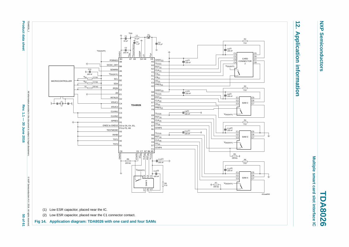
The VCC(n) voltage should be decoupled with two low ESR 100 nF (minimum) capacitors. One capacitor should be placed close to the VCC pin of the device and the other close to the C1 pin of the card connector. See Figure 14 for detailed information.
8.8 Sequencer and clock counter
Each card slot has a dedicated sequencer and clock counter.
The sequencer ensures that the activation and deactivation sequences meet the ISO 7816 and EMV 4.3 standards, even during an emergency deactivation caused by card removal during transaction, supply drop out or a hardware problem. The sequencer is clocked with an internal oscillator (fosc(int)).
Product data sheet Rev. 1.1 — 30 June 2016 33 of 61
NXP Semiconductors TDA8026Multiple smart card slot interface IC
Card slot 1 or card slot 2 can only be activated if a card is detected as present in the slot and if an alarm is not triggered by the voltage supervisor. When both of these parameters are met, the card slots can be activated by setting the Command register START bit. The activation sequence is described in Section 8.8.2.
Card slots 3 to 5 do not have presence monitoring. The corresponding STAP pin is used for card presence detection on these slots.
The deactivation is initiated by the system controller or automatically in the case of a hardware problem or a supply drop out. The deactivation sequence is described in Section 8.8.3.
Outside a session, the card contacts are forced to low-impedance with respect to the GNDC pin.
8.8.1 Standby mode
Standby mode is the default state after a power-on reset. This mode ensures the power consumption remains low until a card is inserted or the microcontroller starts a card session. When there is not an ongoing card session, the internal oscillator runs at its low frequency (t15).
A debouncing time of 17.8 ms is applied to card slot 1 and card slot 2 to allow for card insertion (presence) detection.
8.8.2 Activation sequence
When the card is inactive, pins VCC(n), CLK(n), RST(n) and I/O(n) are LOW which is low-impedance with respect to pin GNDC(n) or pin GNDS depending of the card slot.
The sequencer is clocked by an internal oscillator. When everything is satisfactory (voltage supply, card presence, no hardware problem), the system controller can trigger the card present activation sequence by setting card slot’s START bit to logic 1:
• The internal oscillator switches to its high frequency (t0, see Figure 10).
• The DC-to-DC converter starts (t1).
• VCC(n) starts to rise from 0 V to 1.8 V, 3 V or 5 V during the controlled rise time (t2).
• The voltage on the I/O(n) pin rises to VCC(n), due to integrated 10 k pull-ups for VCC(n) (t3).
• CLK(n) clock signal is sent to the card (t4 = tact) and the RST(n) pin is enabled. The RST(n) pin is managed by the ATR counter or the Register1 RSTIN bit depending on the card slot mode (asynchronous or synchronous).
The sequencer is clocked by which leads to a time interval T = 25 s (typical).
Product data sheet Rev. 1.1 — 30 June 2016 35 of 61
NXP Semiconductors TDA8026Multiple smart card slot interface IC
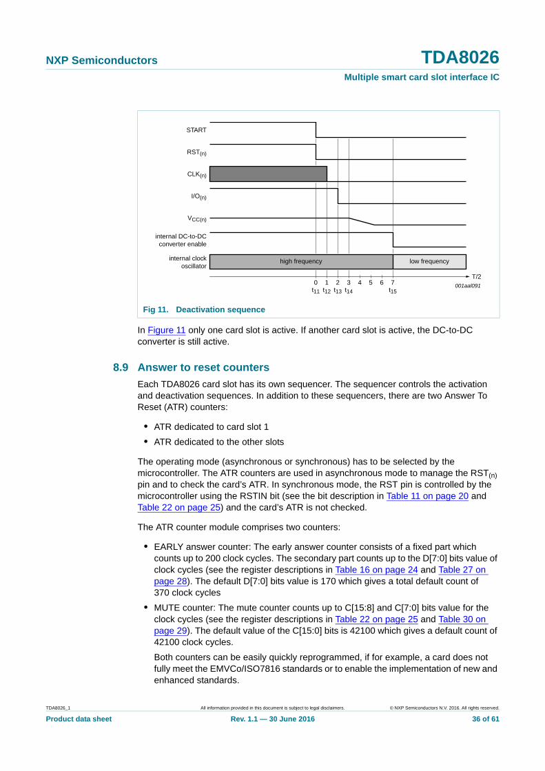
In Figure 11 only one card slot is active. If another card slot is active, the DC-to-DC converter is still active.
8.9 Answer to reset counters
Each TDA8026 card slot has its own sequencer. The sequencer controls the activation and deactivation sequences. In addition to these sequencers, there are two Answer To Reset (ATR) counters:
• ATR dedicated to card slot 1
• ATR dedicated to the other slots
The operating mode (asynchronous or synchronous) has to be selected by the microcontroller. The ATR counters are used in asynchronous mode to manage the RST(n) pin and to check the card’s ATR. In synchronous mode, the RST pin is controlled by the microcontroller using the RSTIN bit (see the bit description in Table 11 on page 20 and Table 22 on page 25) and the card’s ATR is not checked.
The ATR counter module comprises two counters:
• EARLY answer counter: The early answer counter consists of a fixed part which counts up to 200 clock cycles. The secondary part counts up to the D[7:0] bits value of clock cycles (see the register descriptions in Table 16 on page 24 and Table 27 on page 28). The default D[7:0] bits value is 170 which gives a total default count of 370 clock cycles
• MUTE counter: The mute counter counts up to C[15:8] and C[7:0] bits value for the clock cycles (see the register descriptions in Table 22 on page 25 and Table 30 on page 29). The default value of the C[15:0] bits is 42100 which gives a default count of 42100 clock cycles.
Both counters can be easily quickly reprogrammed, if for example, a card does not fully meet the EMVCo/ISO7816 standards or to enable the implementation of new and enhanced standards.
Product data sheet Rev. 1.1 — 30 June 2016 36 of 61
NXP Semiconductors TDA8026Multiple smart card slot interface IC
When operating, the microcontroller starts to configure the selected card slot (card supply voltage) and then triggers the activation sequence using the START bit. The sequencer then performs the activation sequence. The DC-to-DC converter is started, pin VCC(n) is set to the previously configured card supply voltage, pin I/O(n) is enabled and CLK(n) starts (see Section 8.8.2 on page 34 and Section 8.8.3 on page 35). Pin RST(n) is set to LOW.
The ATR counter dedicated to the card slot makes the following checks and takes the steps required:
• START bits from a card detected on pin I/O(n) during the first 200 clock cycles are ignored and the count continues.
• START bits from a card detected while pin RST(n) is set to LOW, with the number of clock cycles between 200 and the C[15:0] bits value (default 42100), cause the EARLY and MUTE bits to be set to logic 1. Pin RST(n) remains LOW and the microcontroller decides if it will accept the card.
• START bits detected after the number of clock cycles is equal to the C[15:0] bits value cause pin RST(n) to be set to HIGH.
• START bits received from the card when the first number of clock cycles is equal to the D[7:0] bits value (default 370) and pin RST(n) set to HIGH cause the EARLY bit to be set to logic 1.
• Cards not answering before 42100 clock cycles (or the C[15:0] bits value) with RST(n) set to HIGH cause the MUTE bit to be set to logic 1.
• Cards answering within the correct time frame, stops the clock cycles count and the microcontroller can send commands to the card.
Figure 12 shows the timings checked by the ATR counters.
When the EARLY and MUTE bits are set to logic 1, they signal an interrupt (see the bit descriptions in Table 12 on page 21, Table 22 on page 25 and Table 36 on page 32).
Product data sheet Rev. 1.1 — 30 June 2016 37 of 61
NXP Semiconductors TDA8026Multiple smart card slot interface IC
The sequence described in Section 8.9 relates to a cold reset. If the card is mute (has not answered), the microcontroller can start a warm reset by setting WARM bit to logic 1 (see the bit descriptions in Table 11 on page 20 and Table 22 on page 25). Then, the ATR counter set pin RST(n) to LOW and performs the same timing checks (see Figure 12).
Remark: It is assumed that two card activations will not take place simultaneously on card slots 2 to 5 because only one I/O(n) line is available for these four slots. There is no protection on the second ATR counter against starting an activation while a count is ongoing. The first ATR counter is dedicated to the slot 1. Consequently, it is mandatory to enable only one slot I/O(n) line at the same time for card slots 2 to 5. When switching from one slot to another one, it is mandatory to first disable the slot I/O(n) line in use before enabling the slot I/O(n) line required. During this transition, no I/O(n) lines are enabled for card slots 2 to 5. This allows the ATR counter to be reset between card slot switching actions. If both pins I/OUC1 and I/OUC2 are connected at the same time, this mandatory condition also applies to card slot 1.
8.10 Slew rate control
Slew rate control is embedded for the clock buffer and the I/O(n) line of each card slot. The rising and falling edge of the card clock signal can be configured using 2 bits in Register6 of bank 1. The settings based on a 30 pF load capacitance and a VCC(n) = 5 V are shown in Table 38.
[1] The high slots are define by [1] (slot 1) and [3] (all other slots).
[2] The low slots are define by [0] (slot 1) and [2] (all other slots).
The rise and fall time is calculated from 10 % to 90 % and 90 % to 10 % (respectively) of the signal amplitude. The default setting for CLK_SR[1]/CLK_SR[3] (high) is LOW and CLK_SR[0]/CLK_SR[2] (low) is HIGH.
Only the falling edge of the card I/O(n) signal can be configured with the two programmable bits in Register6 of bank 1. The settings based on a 30 pF load capacitance and a VCC(n) = 5 V are shown in Table 39 on page 38:
[1] The high slots are define by [1] (slot 1) and [3] (all other slots).
[2] The low slots are define by [0] (slot 1) and [2] (all other slots).
Table 38. Clock Slew rate
CLK_SR[1] (high) CLK_SR[2] (low) Rise and fall time (ns)
Product data sheet Rev. 1.1 — 30 June 2016 38 of 61
NXP Semiconductors TDA8026Multiple smart card slot interface IC
The fall time is calculated from 90 % to 10 % of the signal amplitude. The default setting for IO_SR[0]/IO_SR[2] (low) and IO_SR[1]/IO_SR[3] (high) is LOW (see table Table 39 on page 38).
8.11 Fault detection
The following fault conditions are monitored by the TDA8026.
• Overheating: All the card slots are automatically deactivated and the device is forced in to Standby mode when the detected temperature range is between 125 C to 209 C. The card slot PROT bit is set to logic 1. Above 209 C the device is shutdown.
• Card removal during transaction: A deactivation sequence is performed in accordance with the EMV 4.2 standard.
• DC-to-DC converter overload: All card slots are automatically deactivated and the device is placed in Standby mode when the current supplied by the DC-to-DC converter exceeds 170 mA (ICC parameter for VCC(n)). The card slot PROT bit is set to logic 1
• Card slot current limitation and deactivation: A current level drawn by a card which exceeds 120 mA (Isd parameter for VCC(n)) triggers the deactivation sequence on the faulty card slot. During the deactivation, the current is limited to approximately 110 mA. The card slot PROT bit is set to logic 1
• VDD or VDD(INTF) dropping: A voltage drop occurring on VDD or VDD(iNTF) generates card slot deactivation followed by a device reset. The completion of this phase is validated when the SUPL bits are set to logic 1.
Product data sheet Rev. 1.1 — 30 June 2016 39 of 61
NXP Semiconductors TDA8026Multiple smart card slot interface IC
9. Limiting values
[1] The limiting values depend on the external inductor and VUP decoupling capacitor used.
[2] Every pin withstands the ESD test according to MIL-STD-883C class 3 for card contacts, class 2 for the remaining. Method 3015 (HBM; 1500 ; 100 pF) defines three pulses positive and three pulses negative on each pin referenced to ground.
[3] The 7 kV ESD test is performed in the typical application configuration as depicted in the Application note AN10724 with two external capacitors connected to each VCC(n) line.
10. Thermal characteristics
[1] With a 4-layer board
Table 40. Limiting values In accordance with the Absolute Maximum Rating System (IEC 60134).
Product data sheet Rev. 1.1 — 30 June 2016 40 of 61
NXP Semiconductors TDA8026Multiple smart card slot interface IC
11. Characteristics
[1] fclk(ext) is the external clock frequency applied to pins CLKIN1 and CLKIN2.
[2] Refer to Section 8.6 for further information about DC-to-DC converter operation.
[3] See Figure 6 “The voltage supervisor circuit” on page 12.
[4] See Section 8.3.2 “Description” for a description of the voltage supervisor.
[5] Typical value measurement based on a 85 % DC-to-DC converter and inductance efficiency; depends on PCB layout and external component quality (inductor, capacitor).
[6] Maximum measurement value based on a 125 mA ICC current load and a 75 % DC-to-DC converter and inductance efficiency; depends on PCB layout and external component quality (inductor, capacitor).
Product data sheet Rev. 1.1 — 30 June 2016 42 of 61
NXP Semiconductors TDA8026Multiple smart card slot interface IC
ICC supply current Standby mode and pin VCC(n) grounded
- - 1 mA
active mode; 2.7 V < VDD < 5.5 V
5 V card - - 55 mA
3 V card - - 55 mA
1.8 V card - - 35 mA
sum of all card supply currents on pins VCC(n); active mode; All VCC pins = 5 V; fclk(ext) on pins CLK(n) = 5 MHz; ICC(1) = ICC(2) = 55 mA; ICC(3) = ICC(4) = ICC(5) = 2 mA
[5] - 116 125 mA
SR slew rate rising; maximum CL = 200 nF; 5 V, 3 V and 1.8 V cards
0.06 0.16 0.27 V/s
Cdec decoupling capacitance connected to VCC(n); 100 nF and 100 nF at 20 %
160 200 240 nF
Card reset output pins: RST(1) to RST(5)
Vo output voltage Standby mode
no load 0 - 0.1 V
Io = 1 mA 0 - 0.3 V
Io output current Standby mode and pin RST(n) grounded
0 - 1 mA
VOL LOW-level output voltage
IOL 200 A - C2 version 0 - 0.3 V
IOL 200 A - C3 version 0 - 0.15 VCC(n) V
IOL 20 mA VCC(n) 0.4 - VCC(n) V
VOH HIGH-level output voltage
200 A IOH 0 VCC(n) 0.5 - VCC(n) V
20 mA IOH 0 0 - 0.4 V
tr rise time CL = 100 pF; 10 % to 90 % - - 0.1 s
tf fall time CL = 100 pF; 90 % to 10 % - - 0.1 s
Clock to card output pins: CLK(1) to CLK(5); default register values
Vo output voltage Standby mode
no load 0 - 0.1 V
Io = 1 mA 0 - 0.3 V
Io output current Standby mode and CLK(n) pin grounded
Product data sheet Rev. 1.1 — 30 June 2016 44 of 61
NXP Semiconductors TDA8026Multiple smart card slot interface IC
[1] Two ceramic multilayer capacitors of minimum 100 nF with low Equivalent Series Resistance (ESR) should be used in order to meet these specifications.
[2] Output voltage towards the card, including ripple.
[3] I/O(n) pin has an internal 10 k pull-up resistor to VCC(n).
[4] I/OUCn pin has an internal 11 k pull-up resistor to VDD(INTF).
[5] Maximum value measurement based on a 125 mA (sum of all card supply currents on pins VCC(n)) current load and a 75 % DC-to-DC converter and inductance efficiency; depends on PCB layout and external component quality (inductor, capacitor).
[1] Refer to Section 8.8.3 for further information.
Card presence input: pin PRES; active HIGH when SPRES pin = LOW or active LOW when SPRES pin = HIGH
VIL LOW-level input voltage 0.3 - +0.2 VDD(INTF) V
VIH HIGH-level input voltage 0.8 VDD(INTF) - VDD(INTF) + 0.3 V
Product data sheet Rev. 1.1 — 30 June 2016 47 of 61
NXP Semiconductors TDA8026Multiple smart card slot interface IC
[1] I/OUCn pin has an internal 11 k pull-up resistor to VDD(INTF).
[2] The hold time required (not greater than 300 ns) to bridge the undefined region of the falling edge of SCL must be internally provided by a transmitter.
Serial data input/output pin: SDA; open-drain
VIL LOW-level input voltage
0.3 - +0.3 VDD(INTF) V
VIH HIGH-level input voltage
0.7 VDD(INTF) - VDD(INTF) + 0.3 V
VOL LOW-level output voltage
IOL = 3 mA - - 0.3 V
ILH HIGH-level leakage current
I/O - - 1 A
ILL LOW-level leakage current
depending on the pull-up resistance; input or output
- - 1 A
Serial clock input pin: SCL
VIL LOW-level input voltage
0.3 - +0.3 VDD(INTF) V
VIH HIGH-level input voltage
0.7 VDD(INTF) - VDD(INTF) + 0.3 V
ILIH HIGH-level input leakage current
- - 1 A
IIL LOW-level input current
depends on the pull-up resistance
- - 1 A
I2C-bus timing; see Figure 13
fSCL SCL clock frequency 0 - 400 kHz
tBUF bus free time between a STOP and START condition
1.3 - - s
tHD;STA hold time (repeated) START condition
hold time after which first clock pulse is generated
0.6 - - s
tLOW LOW period of the SCL clock
1.3 - - s
tHIGH HIGH period of the SCL clock
0.6 - - s
tSU;STA set-up time for a repeated START condition
0.6 - - s
tHD;DAT data hold time [2] 0 - - ns
tSU;DAT data set-up time 100 - - ns
tr rise time both SDA and SCL signals; 10 % to 90 %
- - 300 ns
tf fall time both SDA and SCL signals; 90 % to 10 %
Product data sheet Rev. 1.1 — 30 June 2016 51 of 61
NXP Semiconductors TDA8026Multiple smart card slot interface IC
14. Soldering of SMD packages
This text provides a very brief insight into a complex technology. A more in-depth account of soldering ICs can be found in Application Note AN10365 “Surface mount reflow soldering description”.
14.1 Introduction to soldering
Soldering is one of the most common methods through which packages are attached to Printed Circuit Boards (PCBs), to form electrical circuits. The soldered joint provides both the mechanical and the electrical connection. There is no single soldering method that is ideal for all IC packages. Wave soldering is often preferred when through-hole and Surface Mount Devices (SMDs) are mixed on one printed wiring board; however, it is not suitable for fine pitch SMDs. Reflow soldering is ideal for the small pitches and high densities that come with increased miniaturization.
14.2 Wave and reflow soldering
Wave soldering is a joining technology in which the joints are made by solder coming from a standing wave of liquid solder. The wave soldering process is suitable for the following:
• Through-hole components
• Leaded or leadless SMDs, which are glued to the surface of the printed circuit board
Not all SMDs can be wave soldered. Packages with solder balls, and some leadless packages which have solder lands underneath the body, cannot be wave soldered. Also, leaded SMDs with leads having a pitch smaller than ~0.6 mm cannot be wave soldered, due to an increased probability of bridging.
The reflow soldering process involves applying solder paste to a board, followed by component placement and exposure to a temperature profile. Leaded packages, packages with solder balls, and leadless packages are all reflow solderable.
Key characteristics in both wave and reflow soldering are:
• Board specifications, including the board finish, solder masks and vias
• Package footprints, including solder thieves and orientation
• The moisture sensitivity level of the packages
• Package placement
• Inspection and repair
• Lead-free soldering versus SnPb soldering
14.3 Wave soldering
Key characteristics in wave soldering are:
• Process issues, such as application of adhesive and flux, clinching of leads, board transport, the solder wave parameters, and the time during which components are exposed to the wave
• Solder bath specifications, including temperature and impurities
Product data sheet Rev. 1.1 — 30 June 2016 52 of 61
NXP Semiconductors TDA8026Multiple smart card slot interface IC
14.4 Reflow soldering
Key characteristics in reflow soldering are:
• Lead-free versus SnPb soldering; note that a lead-free reflow process usually leads to higher minimum peak temperatures (see Figure 16) than a SnPb process, thus reducing the process window
• Solder paste printing issues including smearing, release, and adjusting the process window for a mix of large and small components on one board
• Reflow temperature profile; this profile includes preheat, reflow (in which the board is heated to the peak temperature) and cooling down. It is imperative that the peak temperature is high enough for the solder to make reliable solder joints (a solder paste characteristic). In addition, the peak temperature must be low enough that the packages and/or boards are not damaged. The peak temperature of the package depends on package thickness and volume and is classified in accordance with Table 49 and 50
Moisture sensitivity precautions, as indicated on the packing, must be respected at all times.
Studies have shown that small packages reach higher temperatures during reflow soldering, see Figure 16.
Table 49. SnPb eutectic process (from J-STD-020C)
Package thickness (mm) Package reflow temperature (C)
Volume (mm3)
< 350 350
< 2.5 235 220
2.5 220 220
Table 50. Lead-free process (from J-STD-020C)
Package thickness (mm) Package reflow temperature (C)
Product data sheet Rev. 1.1 — 30 June 2016 55 of 61
NXP Semiconductors TDA8026Multiple smart card slot interface IC
17. Legal information
17.1 Data sheet status
[1] Please consult the most recently issued document before initiating or completing a design.
[2] The term ‘short data sheet’ is explained in section “Definitions”.
[3] The product status of device(s) described in this document may have changed since this document was published and may differ in case of multiple devices. The latest product status information is available on the Internet at URL http://www.nxp.com.
17.2 Definitions
Draft — The document is a draft version only. The content is still under internal review and subject to formal approval, which may result in modifications or additions. NXP Semiconductors does not give any representations or warranties as to the accuracy or completeness of information included herein and shall have no liability for the consequences of use of such information.
Short data sheet — A short data sheet is an extract from a full data sheet with the same product type number(s) and title. A short data sheet is intended for quick reference only and should not be relied upon to contain detailed and full information. For detailed and full information see the relevant full data sheet, which is available on request via the local NXP Semiconductors sales office. In case of any inconsistency or conflict with the short data sheet, the full data sheet shall prevail.
Product specification — The information and data provided in a Product data sheet shall define the specification of the product as agreed between NXP Semiconductors and its customer, unless NXP Semiconductors and customer have explicitly agreed otherwise in writing. In no event however, shall an agreement be valid in which the NXP Semiconductors product is deemed to offer functions and qualities beyond those described in the Product data sheet.
17.3 Disclaimers
Limited warranty and liability — Information in this document is believed to be accurate and reliable. However, NXP Semiconductors does not give any representations or warranties, expressed or implied, as to the accuracy or completeness of such information and shall have no liability for the consequences of use of such information.
In no event shall NXP Semiconductors be liable for any indirect, incidental, punitive, special or consequential damages (including - without limitation - lost profits, lost savings, business interruption, costs related to the removal or replacement of any products or rework charges) whether or not such damages are based on tort (including negligence), warranty, breach of contract or any other legal theory.
Notwithstanding any damages that customer might incur for any reason whatsoever, NXP Semiconductors’ aggregate and cumulative liability towards customer for the products described herein shall be limited in accordance with the Terms and conditions of commercial sale of NXP Semiconductors.
Right to make changes — NXP Semiconductors reserves the right to make changes to information published in this document, including without limitation specifications and product descriptions, at any time and without notice. This document supersedes and replaces all information supplied prior to the publication hereof.
Suitability for use — NXP Semiconductors products are not designed, authorized or warranted to be suitable for use in medical, military, aircraft, space or life support equipment, nor in applications where failure or
malfunction of an NXP Semiconductors product can reasonably be expected to result in personal injury, death or severe property or environmental damage. NXP Semiconductors accepts no liability for inclusion and/or use of NXP Semiconductors products in such equipment or applications and therefore such inclusion and/or use is at the customer’s own risk.
Applications — Applications that are described herein for any of these products are for illustrative purposes only. NXP Semiconductors makes no representation or warranty that such applications will be suitable for the specified use without further testing or modification.
NXP Semiconductors does not accept any liability related to any default, damage, costs or problem which is based on a weakness or default in the customer application/use or the application/use of customer’s third party customer(s) (hereinafter both referred to as “Application”). It is customer’s sole responsibility to check whether the NXP Semiconductors product is suitable and fit for the Application planned. Customer has to do all necessary testing for the Application in order to avoid a default of the Application and the product. NXP Semiconductors does not accept any liability in this respect.
Limiting values — Stress above one or more limiting values (as defined in the Absolute Maximum Ratings System of IEC 60134) will cause permanent damage to the device. Limiting values are stress ratings only and (proper) operation of the device at these or any other conditions above those given in the Recommended operating conditions section (if present) or the Characteristics sections of this document is not warranted. Constant or repeated exposure to limiting values will permanently and irreversibly affect the quality and reliability of the device.
Terms and conditions of commercial sale — NXP Semiconductors products are sold subject to the general terms and conditions of commercial sale, as published at http://www.nxp.com/profile/terms, unless otherwise agreed in a valid written individual agreement. In case an individual agreement is concluded only the terms and conditions of the respective agreement shall apply. NXP Semiconductors hereby expressly objects to applying the customer’s general terms and conditions with regard to the purchase of NXP Semiconductors products by customer.
No offer to sell or license — Nothing in this document may be interpreted or construed as an offer to sell products that is open for acceptance or the grant, conveyance or implication of any license under any copyrights, patents or other industrial or intellectual property rights.
Export control — This document as well as the item(s) described herein may be subject to export control regulations. Export might require a prior authorization from national authorities.
Quick reference data — The Quick reference data is an extract of the product data given in the Limiting values and Characteristics sections of this document, and as such is not complete, exhaustive or legally binding.
Non-automotive qualified products — Unless this data sheet expressly states that this specific NXP Semiconductors product is automotive qualified, the product is not suitable for automotive use. It is neither qualified nor tested in accordance with automotive testing or application requirements. NXP Semiconductors accepts no liability for inclusion and/or use of non-automotive qualified products in automotive equipment or applications.
NXP Semiconductors TDA8026Multiple smart card slot interface IC
In the event that customer uses the product for design-in and use in automotive applications to automotive specifications and standards, customer (a) shall use the product without NXP Semiconductors’ warranty of the product for such automotive applications, use and specifications, and (b) whenever customer uses the product for automotive applications beyond NXP Semiconductors’ specifications such use shall be solely at customer’s own risk, and (c) customer fully indemnifies NXP Semiconductors for any liability, damages or failed product claims resulting from customer design and use of the product for automotive applications beyond NXP Semiconductors’ standard warranty and NXP Semiconductors’ product specifications.
17.4 TrademarksNotice: All referenced brands, product names, service names and trademarks are the property of their respective owners.
I2C-bus — logo is a trademark of NXP B.V.
18. Contact information
For more information, please visit: http://www.nxp.com
For sales office addresses, please send an email to: [email protected]
For more information, please visit: http://www.nxp.comFor sales office addresses, please send an email to: [email protected]
Date of release: 30 June 2016
Document identifier: TDA8026_1
Please be aware that important notices concerning this document and the product(s) described herein, have been included in section ‘Legal information’.