2
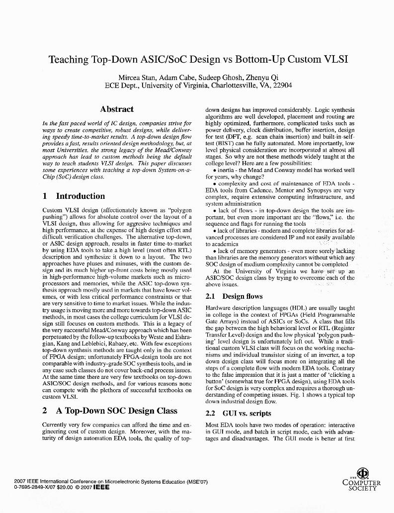
Teaching Top-Down ASICISoC Design vs Bottom-Up Custom VLSI Mircea Stan, Adam Cabe, Sudeep Ghosh, Zhenyu Qi ECE Dept., University of Virginia, Charlottesville, VA, 22904 Abstract In the fast paced world of IC design, companies strive for ways to create competitive, robust designs, while deliver- ing speedy time-to-market results. A top-down design flow provides a fast, results oriented design methodology, but, at most Universities, the strong legacy of the MeadKonway approach has lead to custom methods being the default way to teach students VLSI design. This paper discusses some experiences with teaching a top-down Sysrem-on-a- Chip (SoC)design class. 1 Introduction Custom VLSI design (affectionately known as "polygon pushing") allows for absolute control over the layout of a VLSI design, thus allowing for aggresive techniques and high performance, at the expense of high design effort and difficult verification challenges. The alternative top-down, or ASIC design approach, results in faster time-to-market by using EDA tools to take a high level (most often RTL) description and synthesize it down to a layout. The two approaches have pluses and minuses, with the custom de- sign and its much higher up-front costs being mostly used in high-performance high-volume markets such as micro- processors and memories, while the ASIC top-down syn- thesis approach mostly used in markets that have lower vol- umes, or with less critical performance constraints or that are very sensitive to time tomarket issues. While the indus- try usage is moving more and more towards top-down ASIC methods, in most cases the college curriculum for VLSI de- sign still focuses on custom methods. This is a legacy of the very successful MeadJConway approach which has been perpetuated by the follow-up textbooks by Weste and Eshra- gian, Kang and Leblebici, Rabaey, etc. With few exceptions top-down synthesis methods are taught only in the context of FPGA design; unfortunately FPGA-design tools are not comparable with industry-grade SOC synthesis tools, and in any case such classes do not cover back-end process issues. At the same time there are very few textbooks on top-down ASICISOC design methods, and for various reasons none can compete with the plethora of successful textbooks on custom VLSI. 2 A Top-Down SOC Design Class Currently very few companies can afford the time and en- gineering cost of custom design. Moreover, with the ma- turity of design automation EDA tools, the quality of top- down designs has improved considerably. Logic synthesis algorithms are well developed, placement and routing are highly optimized, furthermore, complicated tasks such as power delivery, clock distribution, buffer insertion, design for test @FT, e.g. scan chain insertion) and built-in-self- test (BIST) can be fully automated. More importantly, low level physical consideration are incorporated at almost all stages. So why are not these methods widely taught at the college level? Here are a few possibilities: inertia - the Mead and Conway model has worked well for years, why change? complexity and cost of maintenance of EDA tools - EDA tools from Cadence, Mentor and Synopsys are very complex, require extensive computing infrastructure, and system administration lack of flows - in top-down design the tools are im- portant, but even more important are the "flows," i.e. the sequence and flags for running the tools lack of libraries - modem and complete librarits for ad- vanced processes are considered IP and not easily available to academics lack of memory generators - even more sorefy'lakking than libraries are the memory generators without which any SOC design of medium complexity cannot be completed At the University of Virginia we have set' up an ASIC/SOC design class by trying to overcome each of the above issues. 2.1 Design flows Hardware description languages (HDL) are usually taught in college in the context of FPGAs (Field Programmable Gate Arrays) instead of ASICs or SoCs. A class that fills the gap between the high behavioral level or RTL (Register Transfer Level) design and the low physical 'polygon push- ing' level design is unfortunately left out. While a tradi- tional custom VLSI class will focus on the working mecha- nisms and individual transistor sizing of an inverter, a top down design class will focus more on integrating all the steps of a complete flow with modem EDA tools. Contrary to the false impression that it is just a matter of 'clicking a button' (somewhat true for FPGA design), using EDA tools for SoC design is very complex and requires a thorough un- derstanding of competing issues. Fig. 1 shows a typical top down industrial design flow. 2.2 GUI vs. scripts Most EDA tools have two modes of operation: interactive in GUI mode, and batch in script mode, each with advan- tages and disadvantages. The GUI mode is better at first 2007 IEEE International Conference on Microelectronic Systems Education (MSE'07) 0-7695-2849-WO7 $20.00 O 2007 IEEE Q C~~PUTER SOCIETY
![ICT-beleidsplan: Beleid [top-down] & differentiatie [bottom-up]](https://static.documents.pub/doc/80x56/55d566d7bb61eb483a8b46d5/ict-beleidsplan-beleid-top-down-differentiatie-bottom-up.jpg)


