www.ultratecusa.com TEC Note #16: A Straightforward Guide to the Sample Preparation of Curved & Warped IC’s Introduction With the semiconductor industry’s adoption of PCB-based substrates for a majority of semiconductor packages, the incidence of in-package die warpage has grown quickly and dramatically in recent years. The move to backside analysis for testing and FA - driven by increased number and density of metallization layers and the ever decreasing size of transistors - has brought with it a myriad of optical and laser-based techniques. Backside ‘through silicon’ techniques require both a direct line-of-sight with the silicon backside and, in most cases, a mirror-polished silicon backside with an uniform remaining silicon thickness (RST) of less, often much less, than 20% of the starting wafer thickness. Couple the evolving backside analytical needs for thinner, more uniform samples, with a packaging-induced silicon center-to-edge warpage that can run to 200 microns or more on larger die sizes, and it is not hard to see that the resulting ‘perfect storm’ requires an entire new 3D sample preparation skill-set -- along with the development of a range of agile and interactive product solutions to assist the FA engineer. This TEC Note provides a level of knowledge regarding the challenges required to produce an optimized sample for various backside analysis techniques, along with comparing several tried-and-tested protocols for thinning and polishing warped devices. What causes a warped die? Warpage occurs due to thermal expansion (CTE) mismatch between the various components in a BGA-style package [10] -- namely the silicon die, the underfill epoxy, and the (pcb-based) substrate. The substrate has a higher CTE which creates warpage in the silicon chip as the package cools to ambient after the molding/curing process. Though overmolded package types have similar thermal CTE mismatch between materials, since molding occurs on both sides of a substrate, the result is package stress, not die warpage. Complex models exist to predict stresses, however a straightforward analogy is to view warpage as resembling a bimetallic strip. [7, 10] 1
Transcript
www.ultratecusa.com
TEC Note #16:
A Straightforward Guide to the Sample Preparation of Curved & Warped IC’s Introduction With the semiconductor industry’s adoption of PCB-based substrates for a majority of semiconductor packages, the incidence of in-package die warpage has grown quickly
and dramatically in recent years.
The move to backside
analysis for testing and FA -
driven by increased number
and density of metallization layers
and the ever decreasing size of transistors - has brought with it a myriad of optical and laser-based techniques. Backside ‘through silicon’ techniques require both a direct line-of-sight with the silicon backside and, in most cases, a mirror-polished silicon backside with an uniform remaining silicon thickness (RST) of less, often much less, than 20% of the starting wafer thickness. Couple the evolving backside analytical needs for thinner, more uniform samples, with a packaging-induced silicon center-to-edge warpage that can run to 200 microns or more on larger die sizes, and it is not hard to see that the resulting ‘perfect storm’ requires an entire new 3D sample preparation skill-set -- along with the development of a range of agile and interactive product solutions to assist the FA engineer. This TEC Note provides a level of knowledge regarding the challenges required to produce an optimized sample for various backside analysis techniques, along with comparing several tried-and-tested protocols for thinning and polishing warped devices.
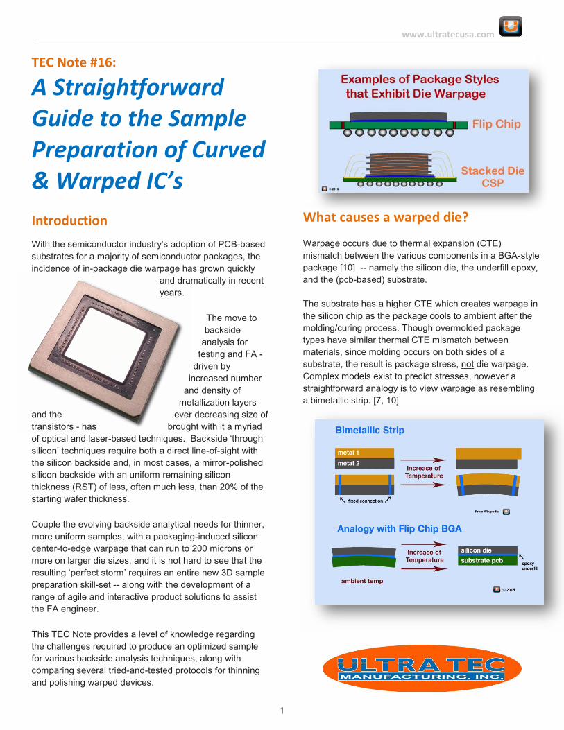
What causes a warped die? Warpage occurs due to thermal expansion (CTE) mismatch between the various components in a BGA-style package [10] -- namely the silicon die, the underfill epoxy, and the (pcb-based) substrate. The substrate has a higher CTE which creates warpage in the silicon chip as the package cools to ambient after the molding/curing process. Though overmolded package types have similar thermal CTE mismatch between materials, since molding occurs on both sides of a substrate, the result is package stress, not die warpage. Complex models exist to predict stresses, however a straightforward analogy is to view warpage as resembling a bimetallic strip. [7, 10]
1
www.ultratecusa.com
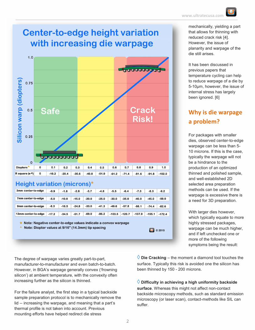
The degree of warpage varies greatly part-to-part, manufacturer-to-manufacturer and even batch-to-batch. However, in BGA’s warpage generally convex (‘frowning silicon’) at ambient temperature, with the convexity often increasing further as the silicon is thinned. For the failure analyst, the first step in a typical backside sample preparation protocol is to mechanically remove the lid -- increasing the warpage, and meaning that a part’s thermal profile is not taken into account. Previous mounting efforts have helped redirect die stress
mechanically, yielding a part that allows for thinning with reduced crack risk [4]. However, the issue of planarity and warpage of the die still arises. It has been discussed in previous papers that temperature cycling can help to reduce warpage of a die by 5-10μm, however, the issue of internal stress has largely been ignored. [6] Why is die warpage a problem? For packages with smaller dies, observed center-to-edge warpage can be less than 5-10 microns. If this is the case, typically the warpage will not be a hindrance to the production of an optimized thinned and polished sample, and well-established 2D selected area preparation methods can be used. If the warpage is excessive there is a need for 3D preparation. With larger dies however, which typically equate to more highly stressed packages, warpage can be much higher, and if left unchecked one or more of the following symptoms being the result:
◊ Die Cracking – the moment a diamond tool touches the surface. Typically this risk is avoided one the silicon has been thinned by 150 - 200 microns. ◊ Difficulty in achieving a high uniformity backside surface. Whereas this might not affect non-contact backside microscopy methods, such as standard emission microscopy (or laser scan), contact-methods like SIL can suffer.
2
www.ultratecusa.com
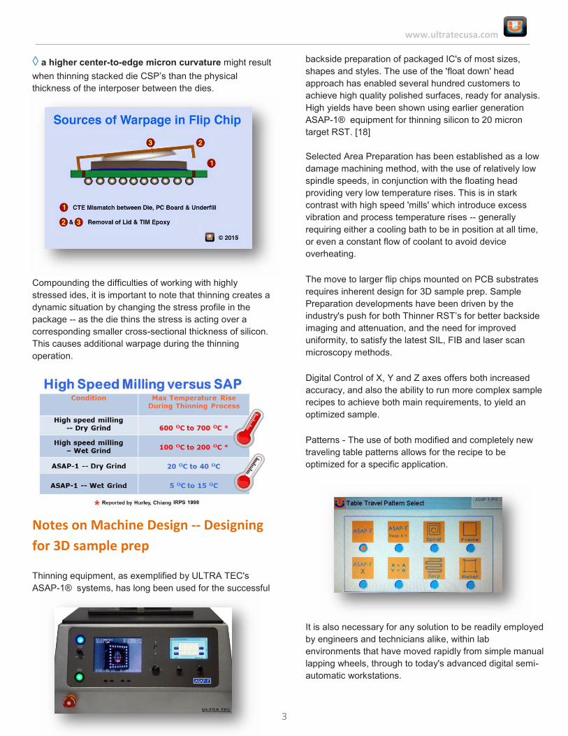
◊ a higher center-to-edge micron curvature might result when thinning stacked die CSP’s than the physical thickness of the interposer between the dies.
Compounding the difficulties of working with highly stressed ides, it is important to note that thinning creates a dynamic situation by changing the stress profile in the package -- as the die thins the stress is acting over a corresponding smaller cross-sectional thickness of silicon. This causes additional warpage during the thinning operation.
Notes on Machine Design -- Designing for 3D sample prep Thinning equipment, as exemplified by ULTRA TEC's ASAP-1® systems, has long been used for the successful
backside preparation of packaged IC's of most sizes, shapes and styles. The use of the 'float down' head approach has enabled several hundred customers to achieve high quality polished surfaces, ready for analysis. High yields have been shown using earlier generation ASAP-1® equipment for thinning silicon to 20 micron target RST. [18] Selected Area Preparation has been established as a low damage machining method, with the use of relatively low spindle speeds, in conjunction with the floating head providing very low temperature rises. This is in stark contrast with high speed 'mills' which introduce excess vibration and process temperature rises -- generally requiring either a cooling bath to be in position at all time, or even a constant flow of coolant to avoid device overheating. The move to larger flip chips mounted on PCB substrates requires inherent design for 3D sample prep. Sample Preparation developments have been driven by the industry's push for both Thinner RST’s for better backside imaging and attenuation, and the need for improved uniformity, to satisfy the latest SIL, FIB and laser scan microscopy methods. Digital Control of X, Y and Z axes offers both increased accuracy, and also the ability to run more complex sample recipes to achieve both main requirements, to yield an optimized sample. Patterns - The use of both modified and completely new traveling table patterns allows for the recipe to be optimized for a specific application.
It is also necessary for any solution to be readily employed by engineers and technicians alike, within lab environments that have moved rapidly from simple manual lapping wheels, through to today's advanced digital semi-automatic workstations.
3
www.ultratecusa.com
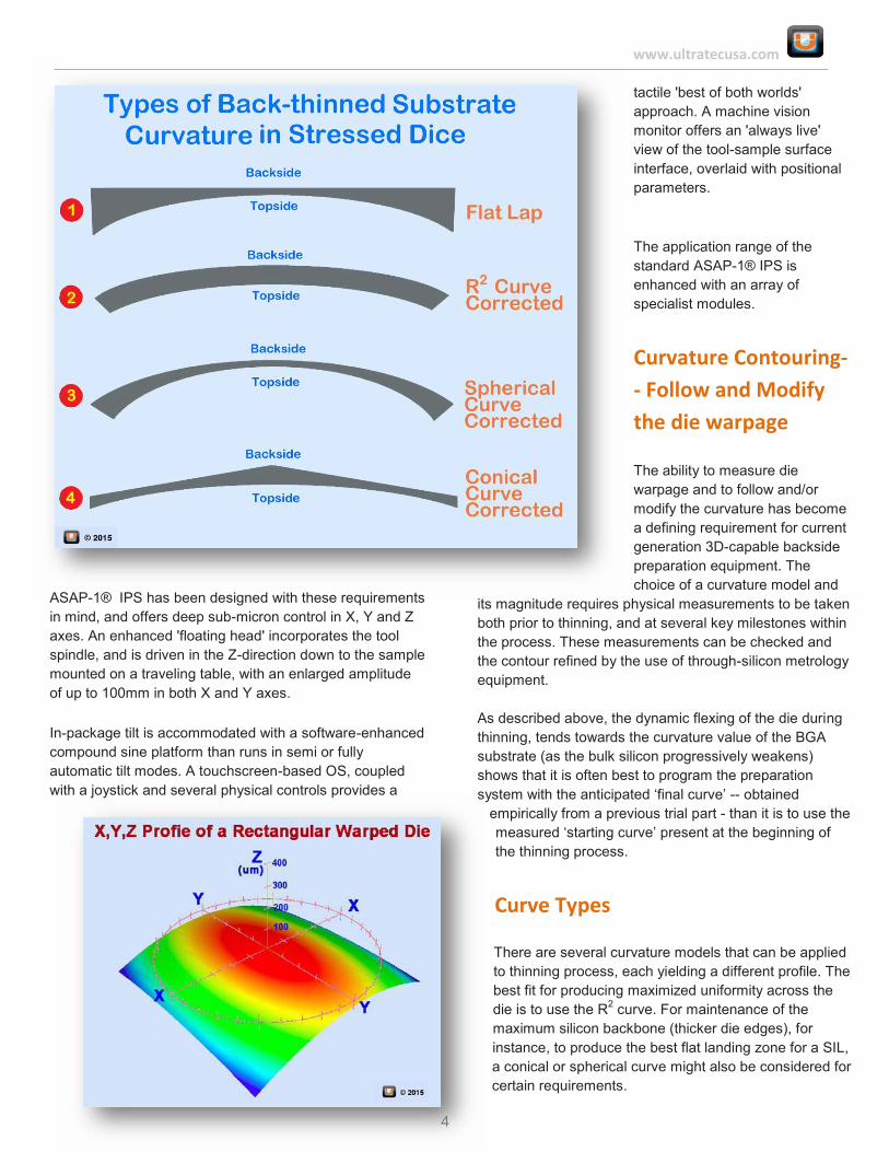
ASAP-1® IPS has been designed with these requirements in mind, and offers deep sub-micron control in X, Y and Z axes. An enhanced 'floating head' incorporates the tool spindle, and is driven in the Z-direction down to the sample mounted on a traveling table, with an enlarged amplitude of up to 100mm in both X and Y axes. In-package tilt is accommodated with a software-enhanced compound sine platform than runs in semi or fully automatic tilt modes. A touchscreen-based OS, coupled with a joystick and several physical controls provides a
tactile 'best of both worlds' approach. A machine vision monitor offers an 'always live' view of the tool-sample surface interface, overlaid with positional parameters. The application range of the standard ASAP-1® IPS is enhanced with an array of specialist modules.
Curvature Contouring-- Follow and Modify the die warpage The ability to measure die warpage and to follow and/or modify the curvature has become a defining requirement for current generation 3D-capable backside preparation equipment. The choice of a curvature model and
its magnitude requires physical measurements to be taken both prior to thinning, and at several key milestones within the process. These measurements can be checked and the contour refined by the use of through-silicon metrology equipment. As described above, the dynamic flexing of the die during thinning, tends towards the curvature value of the BGA substrate (as the bulk silicon progressively weakens) shows that it is often best to program the preparation system with the anticipated ‘final curve’ -- obtained
empirically from a previous trial part - than it is to use the measured ‘starting curve’ present at the beginning of the thinning process. Curve Types There are several curvature models that can be applied to thinning process, each yielding a different profile. The best fit for producing maximized uniformity across the die is to use the R2 curve. For maintenance of the maximum silicon backbone (thicker die edges), for instance, to produce the best flat landing zone for a SIL, a conical or spherical curve might also be considered for certain requirements.
4
www.ultratecusa.com
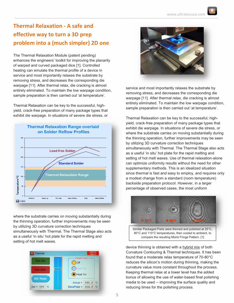
Thermal Relaxation - A safe and effective way to turn a 3D prep problem into a (much simpler) 2D one The Thermal Relaxation Module (patent pending) enhances the engineers’ toolkit for improving the planarity of warped and curved packaged dice [1]. Controlled heating can emulate the thermal profile of a device in service and most importantly relaxes the substrate by removing stress, and decreases the corresponding die warpage [11]. After thermal relax, die cracking is almost entirely eliminated. To maintain the low warpage condition, sample preparation is then carried out ‘at temperature’. Thermal Relaxation can be key to the successful, high-yield, crack-free preparation of many package types that exhibit die warpage. In situations of severe die stress, or
where the substrate carries on moving substantially during the thinning operation, further improvements may be seen by utilizing 3D curvature correction techniques simultaneously with Thermal. The Thermal Stage also acts as a useful ‘in situ’ hot plate for the rapid melting and setting of hot melt waxes.
service and most importantly relaxes the substrate by removing stress, and decreases the corresponding die warpage [11] After thermal relax, die cracking is almost entirely eliminated. To maintain the low warpage condition, sample preparation is then carried out ‘at temperature’. Thermal Relaxation can be key to the successful, high-yield, crack-free preparation of many package types that exhibit die warpage. In situations of severe die stress, or where the substrate carries on moving substantially during the thinning operation, further improvements may be seen by utilizing 3D curvature correction techniques simultaneously with Thermal. The Thermal Stage also acts as a useful ‘in situ’ hot plate for the rapid melting and setting of hot melt waxes. Use of thermal relaxation-alone can optimize uniformity results without the need for other supplementary methods. This is an idealized situation since thermal is fast and easy to employ, and requires only a modest change from a standard (room temperature) backside preparation protocol. However, in a larger percentage of observed cases, the most uniform
device thinning is obtained with a hybrid mix of both Curvature Contouring & Thermal techniques. It has been found that a moderate relax temperature of 70-80°C reduces the silicon’s motion during thinning, making the curvature value more constant throughout the process. Keeping thermal relax at a lower level has the added bonus of allowing the use of water-based final polishing media to be used -- improving the surface quality and reducing times for the polishing process.
Similar Packaged Parts were thinned and polished at 25°C, 80°C and 110°C temperatures, then cooled to ambient, to
compare the resulting Moiré Fringe Pattern. [1]
5
www.ultratecusa.com
Measuring Remaining Silicon Thickness (RST)
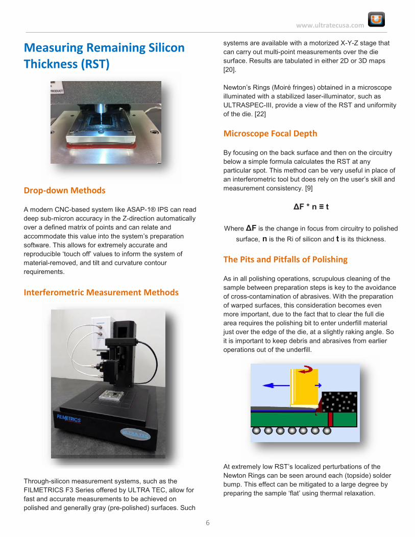
Drop-down Methods A modern CNC-based system like ASAP-1® IPS can read deep sub-micron accuracy in the Z-direction automatically over a defined matrix of points and can relate and accommodate this value into the system’s preparation software. This allows for extremely accurate and reproducible ‘touch off’ values to inform the system of material-removed, and tilt and curvature contour requirements. Interferometric Measurement Methods
Through-silicon measurement systems, such as the FILMETRICS F3 Series offered by ULTRA TEC, allow for fast and accurate measurements to be achieved on polished and generally gray (pre-polished) surfaces. Such
systems are available with a motorized X-Y-Z stage that can carry out multi-point measurements over the die surface. Results are tabulated in either 2D or 3D maps [20]. Newton’s Rings (Moiré fringes) obtained in a microscope illuminated with a stabilized laser-illuminator, such as ULTRASPEC-III, provide a view of the RST and uniformity of the die. [22]
Microscope Focal Depth By focusing on the back surface and then on the circuitry below a simple formula calculates the RST at any particular spot. This method can be very useful in place of an interferometric tool but does rely on the user’s skill and measurement consistency. [9]
ΔF * n ≡ t
Where ΔF is the change in focus from circuitry to polished surface, n is the Ri of silicon and t is its thickness.
The Pits and Pitfalls of Polishing As in all polishing operations, scrupulous cleaning of the sample between preparation steps is key to the avoidance of cross-contamination of abrasives. With the preparation of warped surfaces, this consideration becomes even more important, due to the fact that to clear the full die area requires the polishing bit to enter underfill material just over the edge of the die, at a slightly raking angle. So it is important to keep debris and abrasives from earlier operations out of the underfill.
At extremely low RST’s localized perturbations of the Newton Rings can be seen around each (topside) solder bump. This effect can be mitigated to a large degree by preparing the sample ‘flat’ using thermal relaxation.
6
www.ultratecusa.com
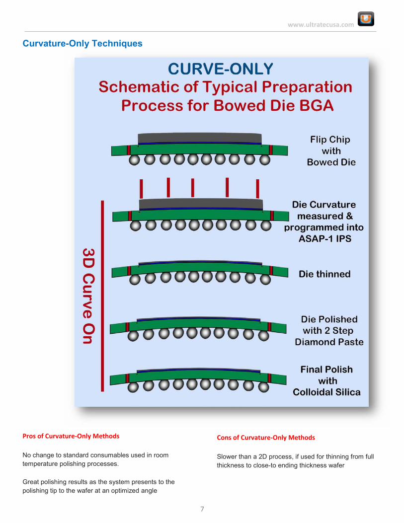
Curvature-Only Techniques Pros of Curvature-Only Methods No change to standard consumables used in room temperature polishing processes. Great polishing results as the system presents to the polishing tip to the wafer at an optimized angle
Cons of Curvature-Only Methods Slower than a 2D process, if used for thinning from full thickness to close-to ending thickness wafer
7
www.ultratecusa.com
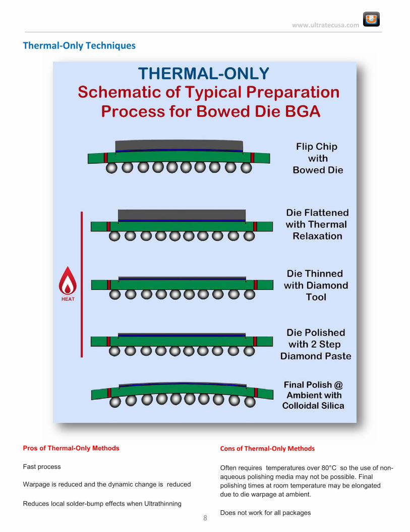
Thermal-Only Techniques Pros of Thermal-Only Methods Fast process Warpage is reduced and the dynamic change is reduced Reduces local solder-bump effects when Ultrathinning
Cons of Thermal-Only Methods Often requires temperatures over 80°C so the use of non-aqueous polishing media may not be possible. Final polishing times at room temperature may be elongated due to die warpage at ambient. Does not work for all packages
8
www.ultratecusa.com
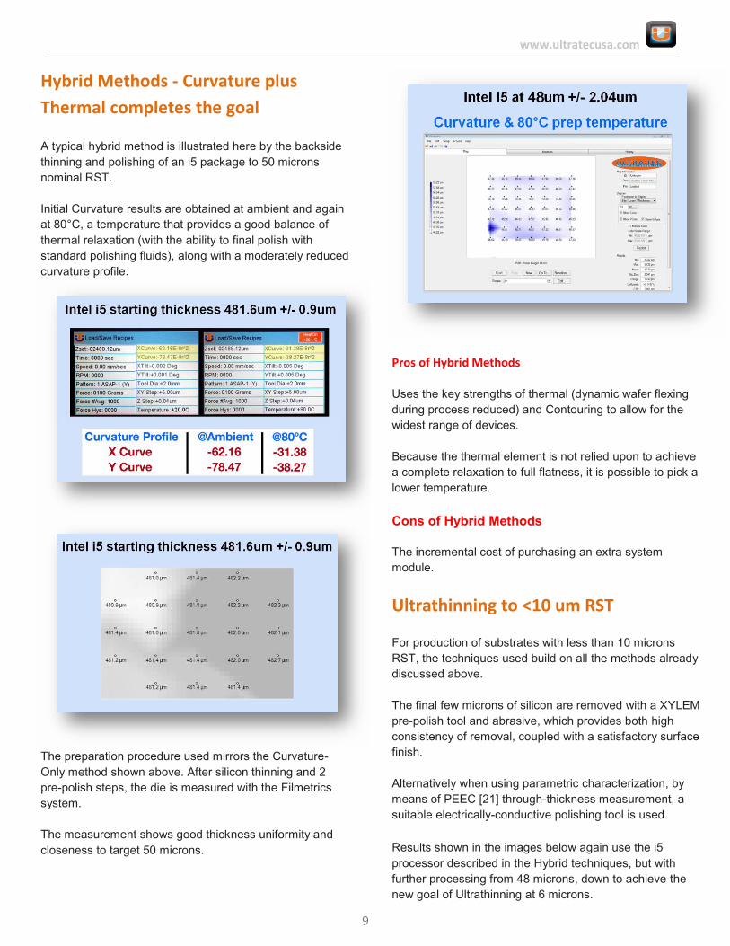
Hybrid Methods - Curvature plus Thermal completes the goal A typical hybrid method is illustrated here by the backside thinning and polishing of an i5 package to 50 microns nominal RST. Initial Curvature results are obtained at ambient and again at 80°C, a temperature that provides a good balance of thermal relaxation (with the ability to final polish with standard polishing fluids), along with a moderately reduced curvature profile.
The preparation procedure used mirrors the Curvature-Only method shown above. After silicon thinning and 2 pre-polish steps, the die is measured with the Filmetrics system. The measurement shows good thickness uniformity and closeness to target 50 microns.
Pros of Hybrid Methods Uses the key strengths of thermal (dynamic wafer flexing during process reduced) and Contouring to allow for the widest range of devices. Because the thermal element is not relied upon to achieve a complete relaxation to full flatness, it is possible to pick a lower temperature. Cons of Hybrid Methods The incremental cost of purchasing an extra system module.
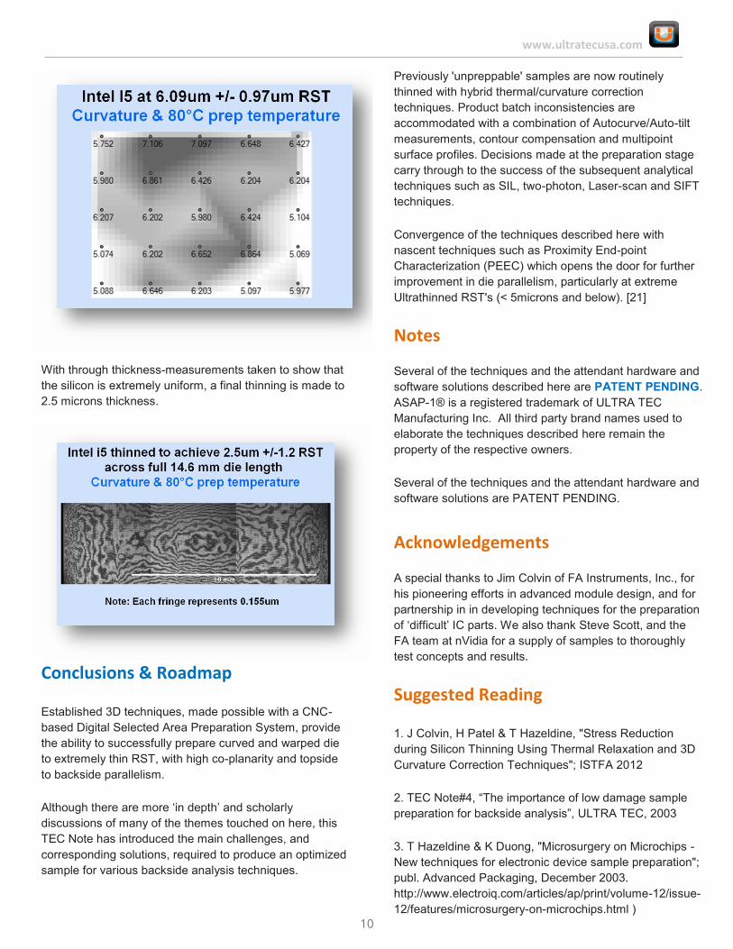
Ultrathinning to <10 um RST For production of substrates with less than 10 microns RST, the techniques used build on all the methods already discussed above. The final few microns of silicon are removed with a XYLEM pre-polish tool and abrasive, which provides both high consistency of removal, coupled with a satisfactory surface finish. Alternatively when using parametric characterization, by means of PEEC [21] through-thickness measurement, a suitable electrically-conductive polishing tool is used. Results shown in the images below again use the i5 processor described in the Hybrid techniques, but with further processing from 48 microns, down to achieve the new goal of Ultrathinning at 6 microns.
9
www.ultratecusa.com
With through thickness-measurements taken to show that the silicon is extremely uniform, a final thinning is made to 2.5 microns thickness.
Conclusions & Roadmap Established 3D techniques, made possible with a CNC-based Digital Selected Area Preparation System, provide the ability to successfully prepare curved and warped die to extremely thin RST, with high co-planarity and topside to backside parallelism. Although there are more ‘in depth’ and scholarly discussions of many of the themes touched on here, this TEC Note has introduced the main challenges, and corresponding solutions, required to produce an optimized sample for various backside analysis techniques.
Previously 'unpreppable' samples are now routinely thinned with hybrid thermal/curvature correction techniques. Product batch inconsistencies are accommodated with a combination of Autocurve/Auto-tilt measurements, contour compensation and multipoint surface profiles. Decisions made at the preparation stage carry through to the success of the subsequent analytical techniques such as SIL, two-photon, Laser-scan and SIFT techniques. Convergence of the techniques described here with nascent techniques such as Proximity End-point Characterization (PEEC) which opens the door for further improvement in die parallelism, particularly at extreme Ultrathinned RST's (< 5microns and below). [21]
Notes Several of the techniques and the attendant hardware and software solutions described here are PATENT PENDING. ASAP-1® is a registered trademark of ULTRA TEC Manufacturing Inc. All third party brand names used to elaborate the techniques described here remain the property of the respective owners. Several of the techniques and the attendant hardware and software solutions are PATENT PENDING. Acknowledgements A special thanks to Jim Colvin of FA Instruments, Inc., for his pioneering efforts in advanced module design, and for partnership in in developing techniques for the preparation of ‘difficult’ IC parts. We also thank Steve Scott, and the FA team at nVidia for a supply of samples to thoroughly test concepts and results.
Suggested Reading 1. J Colvin, H Patel & T Hazeldine, "Stress Reduction during Silicon Thinning Using Thermal Relaxation and 3D Curvature Correction Techniques"; ISTFA 2012 2. TEC Note#4, “The importance of low damage sample preparation for backside analysis”, ULTRA TEC, 2003 3. T Hazeldine & K Duong, "Microsurgery on Microchips - New techniques for electronic device sample preparation"; publ. Advanced Packaging, December 2003. http://www.electroiq.com/articles/ap/print/volume-12/issue-12/features/microsurgery-on-microchips.html )
10
www.ultratecusa.com
4. MM Mulholland and RP Wadell, "A Method of Stress Reduction during Silicon Thinning"; ISTFA 2011 5. T Lundquist, E Delenia, J Harroun and E LeRoy, "Ultra-Thinning of C4 Integrated Circuits for Backside Analysis" Elsevier Science Ltd., pp. 1-5, 2001 6. D Scott, E O'Donnell, T Malik and R Jain, "Global Die UltraThin Silicon for Backside Diagnostics and Circuit Edit" ISTFA 2009 7. Y Li, "Accurate Predictions of Flip Chip BGA Warpage"; IEEE-ECTC 2003 8. W Young and R Budynas, “Roark’s Formulas for Stress & Strain”; 7th Ed., publ. McGraw-Hill, 2002 9. J Colvin, "BGA and Advanced Package Wire to Wire Bonding for Backside Emission Microscopy"; ISTFA 1999 10. DW Garrett, “Elevated Temperature Measurements of Warpage of BGA Packages”; SMT 11. “Thermal Effect on Die Warpage during Back-side Polishing of Flip Chip BGA Device”; Rahman, Wei, Chong, Nasar-Abdat and Narang; IPFA 2013 12. Pecht, Agarwal et al, "Electronic Packaging: Materials and Their Properties"; publ. CRC Press 1999 13. GW Fynn & WJA Powell, "Cutting and Polishing Optical and Electronic Materials"; 2nd Edition. publ. Adam Hilger, 1988 14. S Li, “Chip-Scale Packages and Their Failure Analysis Challenges”; “Microelectronics Failure Analysis Desk Reference”, 6th ed., RJ Ross(Ed), ASM Int’l, 2011,pp 40-48 15. “The State of the Art in Backside Sample Prep”; Jim Colvin, EDFA Vol 4, No.2, 2002 16. “Packages Have Become the New IC’s”; Jim Colvin, EDFA Volume 16, Issue 4, November 2014 17. High-Resolution Backside GMR Magnetic Current Imaging on a Contour-Milled Globally Ultrathin Die”; D Vallet, J Gaudestad, C Richardson, ISTFA 2014 18. “Backside Failure Analysis Techniques: What’s The Gain Of Silicon Getting Thinner”; Boit, Schafer et al; ESREF 2014
19. F Beck, "Integrated Circuit Failure Analysis: A Guide to Preparation Techniques"; publ. John Wiley, 1998 20. Filmetrics F3 Product Literature; http://www.ultratecusa.com/f3-xxt 21. J Colvin, "FemtoFarad/TeraOhm Endpoint Detection for Microsurgery of Integrated Circuit Devices"; ISTFA 2012 Proceedings 22. J Colvin, “Moiré Stabilized Thermal Imaging”; IPFA 2005 23. GW Fynn & WJA Powell, "Cutting and Polishing Optical and Electronic Materials"; 2nd Edition. publ. Adam Hilger, 1988