23
3GPP Radio Prototyping Using Radio420X 1 nutaq.com 3GPP Radio Prototyping Using Radio420X Technical Article

3GPP Radio Prototyping Using Radio420X
1nutaq.com
3GPP Radio Prototyping Using Radio420X
Technical Article

3GPP Radio Prototyping Using Radio420X
1nutaq.com
This application note addresses 3GPP radio design and prototyping when using the Nutaq Radio420X FPGA mezzanine
card (FMC). It discusses the most critical radio requirements as they relate to 3GPP radio conformance testing, namely
TS 51.021 (GSM) and TS 36.141 (LET). Being similar to some extent to LTE, we invite the reader to apply the same methods
and analysis to WCDMA. The main focus is on the GSM DCS1800 pico base station (BTS) and the LTE local area and home
eNB. The scope is limited to FDD in UMTS bands 1, 2, 3 and 4, with a 5 MHz bandwidth for LTE enhanced node B (eNB).
1 INTRODUCTION.............................................................................................................................................................................. 3
2 RADIO420X.CAPABILITIES.AND.RF.PERFORMANCE.......................................................................................................... 4
3 TRANSMITTER.RF.REQUIREMENTS.......................................................................................................................................... 9
3.1 MODULATION ACCURACY: FREQUENCY ERROR, PHASE ERROR AND ERROR VECTOR MAGNITUDE .......9
3.2 ADJACENT CHANNEL POWER ..............................................................................................................................................................12
3.3 NOTE ON OUT OF BAND SPURIOUS EMISSION ...........................................................................................................................13
4 RECEIVER.RF.REQUIREMENTS..................................................................................................................................................14
4.1 REFERENCE SENSITIVITY LEVEL ........................................................................................................................................................ 14
4.2 ADJACENT CHANNEL SELECTIVITY ..................................................................................................................................................15
4.3 RECEIVER INTERMODULATION ........................................................................................................................................................... 18
4.4 BLOCKING PERFORMANCE .................................................................................................................................................................... 19
5 CONCLUSION................................................................................................................................................................................20
6 REFERENCES..................................................................................................................................................................................21
3GPP.Radio.Prototyping.Using.Radio420X
Written by M. Ahmed Ouameur, PhD, MBA
Abstract
Table.of.Content

3GPP Radio Prototyping Using Radio420X
2nutaq.com
Figure 2-1 FMC.Radio420X.board.with.shield.removed................................................................................................................ 4
Figure 2-2 Functional.block.diagram.................................................................................................................................................. 5
Figure 2-3. Radio420X.transmitter.performance:... . a).low.band.from.300.MHz.to.2000.MHz.and... . b).high.band.from.1500.MHz.to.3800.MHz................................................................................................................... 6
Figure 2-4...FMC.Radio420X.RX.filter.banks...................................................................................................................................... 7
Figure 2-5...Radio420X.receiver.performance:... . a).Low.band.from.300.MHz.to.2000.MHz.and... . b).high.band.from.1500.MHz.to.3800.MHz................................................................................................................... 8
Figure 4-1... Narrow.band.and.Wideband.interferer.levels.for.a).local.area.eNB.and.b).home.eNB....................................16
Figure 4-2...Software-selectable.baseband.filters.for.adjacent.channel.selectivity.................................................................17
Table 1-1. GSM.and.LTE.(UMTS).frequency.bands.for.FDD.......................................................................................................... 3
Table 3-1. Required.EVM.for.PDSCH.................................................................................................................................................. 9
Table 3-2. Radio420X.EVM...................................................................................................................................................................11
Table 3-3.. PCS1800.pico’s.modulation.spectrum.and.minimum.VCO.requirement...............................................................12
Table 4-1.. LTE.eNB.reference.sensitivity.level................................................................................................................................14
Table 4-2.. Co-channel.and.adjacent.channel.interference.rejections.for.TCH/FS.................................................................15
Table 4-3.. Intermodulation.performance.requirement.................................................................................................................18
Table 4-4.. Blocking.performance.requirement...............................................................................................................................19
List.of.Figures
List.of.Tables

3GPP Radio Prototyping Using Radio420X
3nutaq.com
Table 1-1 GSM.and.LTE.(UMTS).frequency.bands.for.FDD
. Band. Uplink. Downlink. Band.Gap. Duplex.Separation. GSM. LTE. Comment
. Number. (MHz). (MHz). (MHz). (MHz). Usage. Usage
1 1920–1990 2110–2170 130 190 N Y
2 1850–1910 1930–1990 20 80 Y Y PCS1900
3 1710–1785 1850–1880 20 95 Y Y DCS1800
4 1710–1755 2110–2155 355 400 N Y
1. Introduction
RF transmitters must be designed to generate a clean
signal within the assigned spectrum while keeping
unwanted spurious products within allowable levels.
Likewise, receivers must reliably demodulate the wanted
weak signal while also rejecting interference from
neighbouring channels. Performance requirements for
these RF characteristics aim to ensure that equipment
authorized to operate on GSM or LTE carriers meets certain
minimum standards [1]-[2].
This document focuses on the frequency bands and
arrangements for FDD as shown in Table 1-1. Other
frequency bands and arrangements can be found in
TS 36.141 [2].
The design of the LTE physical layer (PHY) is heavily
influenced by requirements for a high peak transmission
rate (100 Mbps downlink/50 Mbps uplink), multiple channel
bandwidths (1.25 to 20 MHz), and spectral efficiency. To
fulfill these requirements, orthogonal frequency division
multiplexing (OFDM) was selected as the basis for the
physical (PHY) layer. The use of OFDM and multiple-input/
multiple-output (MIMO), two key technologies, significantly
differentiate LTE from other 3G systems such as WCDMA.
LTE adopts different modes of operation (FDD/TDD)
and different downlink and uplink access technologies
(OFDMA, SC-FDMA). GSM, on the other hand, uses GMSK
modulation in both uplink and downlink directions. Time
division multiple access (TDMA) was adopted in GSM as
a multiple access scheme wherein one time frame can
support up to eight users.

3GPP Radio Prototyping Using Radio420X
4nutaq.com
The Radio420X FPGA mezzanine card (FMC) is a powerful
multi-mode software-defined radio (SDR) RF transceiver
module. The Radio420X is designed around the state-of-
the-art, multi-standard, multi-band Lime Microsystems
LMS6002D RF transceiver IC, which supports broadband
coverage, as well as TDD and FDD full duplex modes
of operation [3].
The LMS6002D RF transceiver IC’s bandwidth
(1.5–28 MHz) is selectable on-the-fly, suitable for a large
number of narrowband and broadband applications, and
offers excellent channel selectivity.
Figure 2-1 shows the Radio420X FMC with its shield
removed.
2. Radio420X.capabilities.and.RF.performance
Figure 2-1 FMC Radio420X board with shield removed
3GPP Radio Prototyping Using Radio420X
5nutaq.com
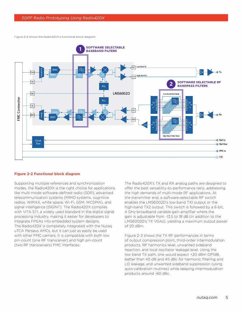
Figure 2-2 Functional block diagram
Supporting multiple references and synchronization
modes, the Radio420X is the right choice for applications
like multi-mode software-defined radio (SDR), advanced
telecommunication systems (MIMO systems, cognitive
radios, WiMAX, white space, Wi-Fi, GSM, WCDMA), and
signal intelligence (SIGINT). The Radio420X complies
with VITA 57.1, a widely used standard in the digital signal
processing industry, making it easier for developers to
integrate FPGAs into embedded system designs.
The Radio420X is completely integrated with the Nutaq
uTCA Perseus AMCs, but it can just as easily be used
with other FMC carriers. It is compatible with both low
pin-count (one RF transceiver) and high pin-count
(two RF transceivers) FMC interfaces.
The Radio420X’s TX and RX analog paths are designed to
offer the best versatility-to-performance ratio, addressing
the high demands of multi-mode RF applications. At
the transmitter end, a software-selectable RF switch
enables the LMS6002D’s low-band TX1 output or the
high-band TX2 output. This switch is followed by a 6-bit,
4 GHz broadband variable gain amplifier where the
gain is adjustable from -13.5 to 18 dB (in addition to the
LMS6002D’s TX VGAs), yielding a maximum output power
of 20 dBm.
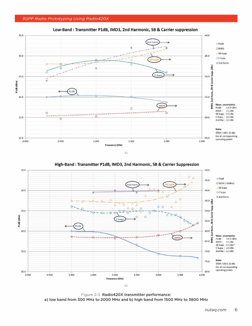
Figure 2-3 shows the TX RF performances in terms
of output compression point, third-order intermodulation
products, RF harmonics level, unwanted sideband
rejection, and local oscillator leakage level. Using the
low band TX path, one would expect +20 dBm OP1dB,
better than 40 dB and 45 dBc for harmonic filtering and
LO leakage, and unwanted sideband suppression (using
auto-calibration routines) while keeping intermodulation
products around -60 dBc.
Figure 2-2 shows the Radio420X’s functional block diagram.
3GPP Radio Prototyping Using Radio420X
6nutaq.com
a)
b)
Figure 2-3 Radio420X.transmitter.performance:.a).low.band.from.300.MHz.to.2000.MHz.and.b).high.band.from.1500.MHz.to.3800.MHz.
3GPP Radio Prototyping Using Radio420X
7nutaq.com
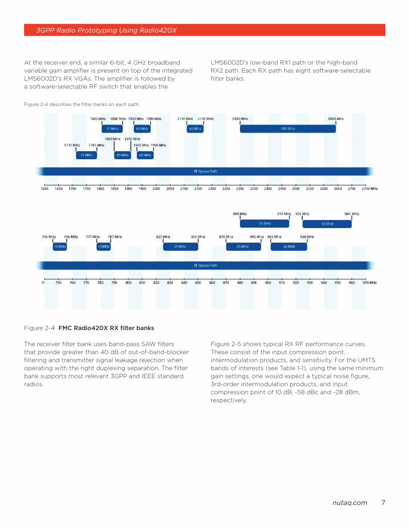
At the receiver end, a similar 6-bit, 4 GHz broadband
variable gain amplifier is present on top of the integrated
LMS6002D’s RX VGAs. The amplifier is followed by
a software-selectable RF switch that enables the
LMS6002D’s low-band RX1 path or the high-band
RX2 path. Each RX path has eight software-selectable
filter banks.
Figure 2-4 FMC.Radio420X.RX.filter.banks
The receiver filter bank uses band-pass SAW filters
that provide greater than 40 dB of out-of-band-blocker
filtering and transmitter signal leakage rejection when
operating with the right duplexing separation. The filter
bank supports most relevant 3GPP and IEEE standard
radios.
Figure 2-5 shows typical RX RF performance curves.
These consist of the input compression point,
intermodulation products, and sensitivity. For the UMTS
bands of interests (see Table 1-1), using the same minimum
gain settings, one would expect a typical noise figure,
3rd-order intermodulation products, and input
compression point of 10 dB, -58 dBc and -28 dBm,
respectively.
Figure 2-4 describes the filter banks on each path.

3GPP Radio Prototyping Using Radio420X
8nutaq.com
a)
b)
Figure 2-5 Radio420X.receiver.performance:.a).Low.band.from.300.MHz.to.2000.MHz.and.b).high.band.from.1500.MHz.to.3800.MHz
In the subsequent sections of this document, we will
demonstrate the Radio420X’s suitability for 3GPP radio
design and prototyping by linking its RF performance
values to frequently used 3GPP metrics, including but
not limited to EVM and ACPR for the transmitter, and
sensitivity and intermodulation attenuation for the receiver.

3GPP Radio Prototyping Using Radio420X
9nutaq.com
This section discusses the implications of GSM and LTE RF performance specifications when designing transmitters.
Transmitters must meet two sets of requirements: those relating to the quality of the intended transmissions, and those
addressing the level of allowable unwanted emissions.
3.1. Modulation.accuracy:.frequency.error,... phase.error.and.error.vector.magnitude
For GSM, GMSK modulation accuracy is measured in
terms of phase error. For the PICO BTS class, the phase
error shall not exceed 5 degrees RMS and 20 degrees
peak while maintaining the mean frequency error across
the burst below 0.1 parts per million (ppm) [1]. The latter
requirement is met with the Radio420X’s high stability
VCTCXO. Phase error is used to verify the correct
implementation of the GMSK modulator and pulse shaping
filtering within the above specified limits under normal and
extreme test conditions and when subjected to vibration.
Analog baseband IQ unbalance and local oscillator (LO)
IQ arms mismatch will also affect phase error. These RF
impairments at the antenna port can be resolved using
an appropriate calibration routine (already supported in
the Radio420X’s calibration software). Care shall also be
taken in PCB layout design to ensure no RF return signal
is fed back from the antenna to the final amplifier stages.
Fortunately, shielding can help for designs with high-
output power levels.
For LTE, error vector magnitude (EVM) is used. EVM is a
measure of the difference between the ideal symbols and
the measured symbols after equalization. The equaliser
parameters are estimated as defined in Annex F of TS
36.141 [2]. The EVM result is defined as the square root
of the ratio of the mean error vector power to the mean
reference power expressed as a percentage. Depending on
the modulation and coding scheme, the purpose of testing
is to verify that the EVM is within the limit specified by the
minimum requirement, as shown in Table 3-1.
Table 3-1 Required.EVM.for.PDSCH
. Modulation.scheme.for.PDSCH. Required.EVM.(%)
QPSK 18.5
16QAM 13.5
64QAM 9
3. Transmitter.RF.requirements
3GPP Radio Prototyping Using Radio420X
10nutaq.com
When used in conjunction with other parameters, EVM
captures the effect of many different signal distortions [4].
It can help pin-point transmit impairments related to:
• Phase noise and frequency error
• IQ imbalance (gain and phase mismatch can create
LO leakage and unwanted sideband components)
• Signal compression effects and nonlinearities
• Spurious components
We will relate EVM to the above signal impairments and
provide quantitative measurements on the Radio420X to
help assess the EVM calculation process.
As far as phase noise is concerned, LO phase noise
consists of random fluctuations around its center
frequency. One common definition is the single sideband
phase noise density L(ƒ) in dBc/Hz for a given frequency
offset ƒ or aggregately in terms of RMS phase noise θrms
in
radian over the information bandwidth. Phase noise affects
modulation accuracy and contributes to EVM. The effect
appears visually as a circular distortion of the signal points
near the center of the constellation.
For example, Let’s look at the Radio420X’s LO phase
noise contribution to EVM. The Radio420X’s LO phase
noise at 2GHz is typically -52dBc/Hz, -70dBc/Hz, -84dBc/
Hz, -88dBc/Hz, -94dBc/Hz, -120dBc/Hz and -136dBc/Hz
at 10Hz, 100Hz, 1kHz, 100kHz, 100kHz 1MHz and 10MHz
offsets, respectively. The calculated RMS phase noise of
0.96o will translate to 1.7% (-35.4 dB) EVM. The following
formula (assuming a high SNR and using 2-order Tailor
series expansion and zero-mean Gaussian distribution for
the phase noise) can be used:
where σ is the RMS LO phase noise.
On the other hand, DC offsets, gain and phase mismatches
in in-phase and quadrature IQ signal paths will directly
affect modulation accuracy. These impairments can be
seen as LO leakage and unwanted sideband rejection
performance. As far as the constellation is concerned
while particularly viewing BPSK pilot symbols, an IQ
gain mismatch would result in pilot symbols spread
mostly along the I-axis, while a phase mismatch would
result in the pilot symbols spread along the Q-axis.
Most transceivers and vector modulators specify these
impairments as LO leakage and single sideband rejection
in dB. A closed form relationship relating to EVM can be
used to assess their contributions as follow
where ACL
and ASSB
are the carrier leakage and single
sideband rejections (SSB) in dB. For reference, the
typical carrier leakage and sideband suppression of the
Radio420X is -45 dB. Both leakages will contribute to
about -45 dB of EVM each. One should also notice the
dB to dB relationship between EVM, carrier leakage, and
unwanted SSB suppressions in high SNR cases.
3GPP Radio Prototyping Using Radio420X
11nutaq.com
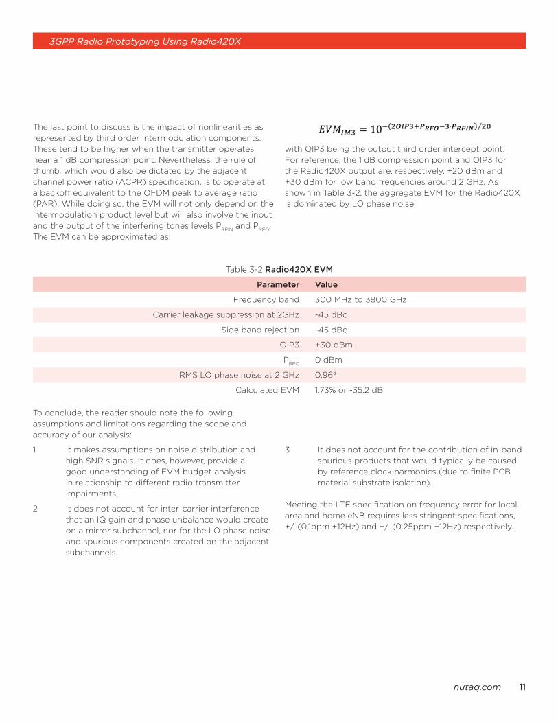
Table 3-2 Radio420X.EVM
. Parameter. Value
Frequency band 300 MHz to 3800 GHz
Carrier leakage suppression at 2GHz -45 dBc
Side band rejection -45 dBc
OIP3 +30 dBm
PRFO
0 dBm
RMS LO phase noise at 2 GHz 0.96°
Calculated EVM 1.73% or -35.2 dB
The last point to discuss is the impact of nonlinearities as
represented by third order intermodulation components.
These tend to be higher when the transmitter operates
near a 1 dB compression point. Nevertheless, the rule of
thumb, which would also be dictated by the adjacent
channel power ratio (ACPR) specification, is to operate at
a backoff equivalent to the OFDM peak to average ratio
(PAR). While doing so, the EVM will not only depend on the
intermodulation product level but will also involve the input
and the output of the interfering tones levels PRFIN
and PRFO
.
The EVM can be approximated as:
with OIP3 being the output third order intercept point.
For reference, the 1 dB compression point and OIP3 for
the Radio420X output are, respectively, +20 dBm and
+30 dBm for low band frequencies around 2 GHz. As
shown in Table 3-2, the aggregate EVM for the Radio420X
is dominated by LO phase noise.
To conclude, the reader should note the following
assumptions and limitations regarding the scope and
accuracy of our analysis:
1 It makes assumptions on noise distribution and
high SNR signals. It does, however, provide a
good understanding of EVM budget analysis
in relationship to different radio transmitter
impairments.
2 It does not account for inter-carrier interference
that an IQ gain and phase unbalance would create
on a mirror subchannel, nor for the LO phase noise
and spurious components created on the adjacent
subchannels.
3 It does not account for the contribution of in-band
spurious products that would typically be caused
by reference clock harmonics (due to finite PCB
material substrate isolation).
Meeting the LTE specification on frequency error for local
area and home eNB requires less stringent specifications,
+/-(0.1ppm +12Hz) and +/-(0.25ppm +12Hz) respectively.

3GPP Radio Prototyping Using Radio420X
12nutaq.com
3.2. Adjacent.channel.power
Table 3-3 PCS1800.pico’s.modulation.spectrum.and.minimum.VCO.requirement
. Frequency. Maximum.limit.per. Maximum.VCO. Radio420X.measured
. offset.in.kHz. TS.51.021.(in.dBc/BW) phase.noise.in.dBc/Hz. phase.noise.@2GHz
+/- 200 -30dBc/30kHz -75 -96
=-30dBc/Hz
-10 Log (30Khz)
+/- 250 -33dBc/30kHz -78 -100
+/- 400 -60dBc/30kHz -105 -108
+/- 600–1200 -60dBc/30kHz -105 -115
+/- 1200–1800 -63dBc/30kHz -108 -120
+/- 1800–6000 -76dBc/100kHz -126 -130
>+/- 6000 -80dBc/100kHz -130 -136
The density of PCBs with small form factors (e.g. FMC) is
a concern in radio design, as many sources of noise and
spurious products may sneak out with the RF signal. The
power supply noise (mainly DC-DC converter switching
noise), for instance, can appear along with the RF signal
close to the carrier (depending on the power supply
switching frequency). Hopefully, these can be contained
within the number of allowed exceptions.
In LTE, the adjacent channel leakage power ratio (ACLR)
is defined as the ratio of the filtered mean power centered
on the assigned channel frequency to the filtered mean
power centered on an adjacent channel frequency. The
requirements apply outside of the RF bandwidth edges,
regardless of the type of transmitter being considered
(single carrier or multi-carrier). The minimum requirement
for Category B eNB (which includes local area and home
eNBs) in paired bands is 44.2 dB or -15 dBm/MHz.
For GSM (GMSK), the modulation, wideband noise and
power level switching spectra can produce significant
interference in the relevant TX and adjacent bands. The
requirements for adjacent channel emissions are tested
by two separate tests that measure different sources
of emission:
• Continuous modulation spectrum and wideband noise
• Switching transients’ spectrum
We will focus on the first item, which is mostly affected by
the transmitter VCO and amplifier stages. The modulation
spectrum puts stringent limitation on VCO phase noise.
For the DCS1800 pico BTS class, the maximum limits are
stated in Table 3-3 and compared to the Radio420X’s
measured phase noise at 2 GHz. This demonstrates that the
Radio420X can meet continuous modulation spectrum and
wideband noise requirements.

3GPP Radio Prototyping Using Radio420X
13nutaq.com
It is interesting to relate ACPR to the 3rd order
intermodulation distortion (IMD3) measured on the
Radio402X. The increase in ACLR is mainly due to
increased adjacent channel occupancy by 3rd and 5th order
intermodulation components [5]. ACLR has been related
to IMD3[5], where an ACLR for n subcarrriers is calculated
using two-tone IMD3 and a correction factor:
with
For a larger number of subcarrriers (as with LTE), a set
of closed form formulas are presented in [5]. [5] relates
ACPR to two-tone intermodulation ratio IMR2 which, in
turn, is linked to third order intercept point IP3 and the
total output power POT
:
Following the established theory in [6-references 1 and 2
therein] the formula for n-tone ACPR is related to IMR2 as
follows:
with N = and M =
for n being an integer multiple of 2.
Asymptotically ACPR will get close to IMR2 when the
number of subcarriers is high. This approximation can be
applied for 20 MHz LTE signals with 2048 subcarriers,
for instance.
For reference, the measured 0 dBm tow-tone IMR2 for
the Radio420X is about -58 dBc at 2 GHz. This suggests
that the expected ACPR is IMR2 with a -24.09 dBm output
power per tone in case of a 5 MHz LTE signal bandwidth.
One would also expect this ACLR level given that the
Radio420X exhibits a typical P1dB of +20 dBm.
Over all, the Radio420X is suitable for LTE radio design
and prototyping at more than +5 dBm of total average
output power. When coupled with off-the-shelf pre-driver
evaluation boards like the SKY77xxx, one can expect a
clear LTE signal at +15 dBm (with more than 12dB back
off) for femtocell applications. GMSK modulation can
operate near compression using less than 3dB backoff,
however, so that one would expect +17 dBm output power
at the antenna connector.
3.3. Out-of-band.spurious.emissions
Spurious emissions in the Radio420X are mostly related to
reference clock harmonics and main RF signal harmonics.
The clock related spurious products are typically measured
at -50dBm/100kHz while the main signal second
harmonic level is at -42 dBc. Operating the Radio420X
at +10 dBm will keep these spurious products below the
recommended FCC limits of -30 dBm (above 1 GHz).
On the other hand, protecting the BTS receiver requires
that spurious emission limitations be set at -88 dBm
in a 100 kHz measurement bandwidth. This translates
into a required VCO phase noise of -138dBm/Hz.
With appropriate TX-RX antenna separation (a few
centimeters), this criteria can easily be met.

3GPP Radio Prototyping Using Radio420X
14nutaq.com
The receiver must reliably demodulate the wanted weak signal, while also rejecting interference from neighbouring
channels. This is addressed by the following requirements: reference sensitivity level, adjacent channel selectivity, receiver
intermodulation, and blocking characteristics.
4.1. Reference.sensitivity.level
GSM defines the static reference sensitivity of the receiver
as the level of signal at the receiver input with a standard
test signal at which the receiver will produce, after
demodulation and channel decoding data with a frame
erasure ratio (FER), a residual bit error ratio (RBER), bit
error ratio (BER), or block error ratio (BLER) better than
or equal to that specified for a specific logical channel
type under static propagation conditions. For the case
of the TCH/FS logical channel, a DCS1800 pico BTS needs
to meet the minimum specifications shown in Table 4-1
with a GMSK signal at -95 dBm [1].
For LTE, the reference sensitivity power level is the
minimum mean power received at the antenna connector
at which a throughput requirement shall be met for
a specified reference measurement channel. To meet
LTE requirements, a throughput of at least 95% of the
maximum throughput shall be achieved with the following
sensitivity level for a 5-MHz channel bandwidth. In
Table 4-1, fixed reference channels A1-3 from [2] are used.
Table 4-1 LTE.eNB.reference.sensitivity.level
. BTS.class. Reference.sensitivity.level.in.dBm. Limits
DCS1800 pico BTS (GSM) -95 FER <0.10 α %
Class Ib RBER < 0.40/α %
Class II RBER 2.0 %
α may be between 1 and 1.6
Local area eNB (LTE) -92.8 Throughput greater than
or equal to 95% of the maximum
throughput
Home eNB (LTE) -92.8 Throughput greater than
or equal to 95% of the maximum
throughput
The typical Radio420X noise figure is 10 dB, which meets the DCS1800 reference sensitivity requirement assuming a
required SNR of 6 dB. For an LTE eNB with QPSK 1/3 modulation and coding scheme (MCS) and a 4.0dB-required SNR
(including a 2 dB implementation margin) a front-end NF of less than 10.2 dB is required.
4. Receiver.RF.requirements
3GPP Radio Prototyping Using Radio420X
15nutaq.com
4.2. Adjacent.channel.selectivity
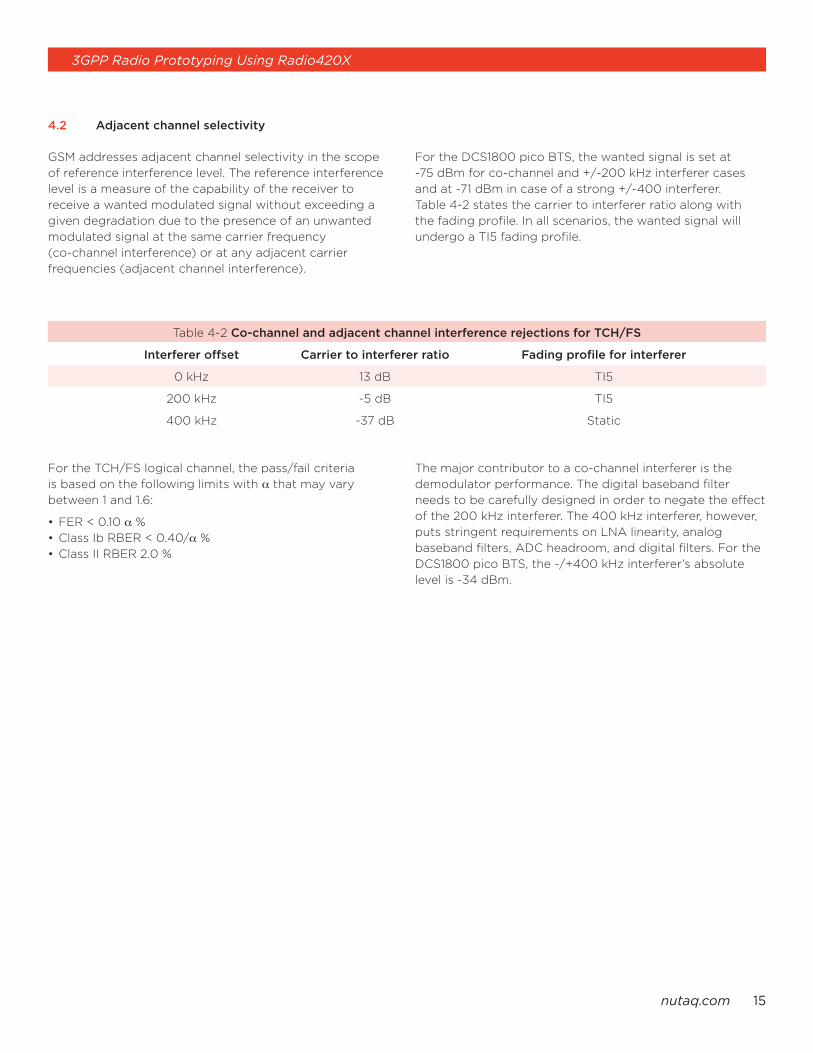
Table 4-2 Co-channel.and.adjacent.channel.interference.rejections.for.TCH/FS
. Interferer.offset. Carrier.to.interferer.ratio. Fading.profile.for.interferer
0 kHz 13 dB TI5
200 kHz -5 dB TI5
400 kHz -37 dB Static
GSM addresses adjacent channel selectivity in the scope
of reference interference level. The reference interference
level is a measure of the capability of the receiver to
receive a wanted modulated signal without exceeding a
given degradation due to the presence of an unwanted
modulated signal at the same carrier frequency
(co-channel interference) or at any adjacent carrier
frequencies (adjacent channel interference).
For the DCS1800 pico BTS, the wanted signal is set at
-75 dBm for co-channel and +/-200 kHz interferer cases
and at -71 dBm in case of a strong +/-400 interferer.
Table 4-2 states the carrier to interferer ratio along with
the fading profile. In all scenarios, the wanted signal will
undergo a TI5 fading profile.
For the TCH/FS logical channel, the pass/fail criteria
is based on the following limits with α that may vary
between 1 and 1.6:
• FER < 0.10 α %
• Class Ib RBER < 0.40/α %
• Class II RBER 2.0 %
The major contributor to a co-channel interferer is the
demodulator performance. The digital baseband filter
needs to be carefully designed in order to negate the effect
of the 200 kHz interferer. The 400 kHz interferer, however,
puts stringent requirements on LNA linearity, analog
baseband filters, ADC headroom, and digital filters. For the
DCS1800 pico BTS, the -/+400 kHz interferer’s absolute
level is -34 dBm.
3GPP Radio Prototyping Using Radio420X
16nutaq.com
a)
b)
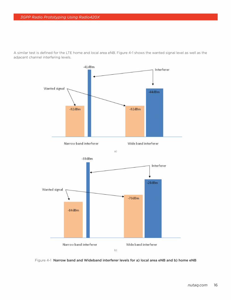
Figure 4-1 Narrow.band.and.Wideband.interferer.levels.for.a).local.area.eNB.and.b).home.eNB
A similar test is defined for the LTE home and local area eNB. Figure 4-1 shows the wanted signal level as well as the
adjacent channel interfering levels.

3GPP Radio Prototyping Using Radio420X
17nutaq.com
Figure 4-2 Software-selectable.baseband.filters.for.adjacent.channel.selectivity
The pass/fail criteria is based on having a throughput of at
least 95% of the maximum throughput. These high signal
levels will put stringent constraints on analog baseband
filter design prior to the ADC. Being part of the integrated
transceiver, the Radio420X’s software-selectable baseband
filters meet the adjacent channel selectivity requirements
given their sharp rejection as shown in Figure 4-2.
The Radio420X’s operation relies on the use of gain
settings to avoid receiver saturation (ADC saturation
mainly). Nevertheless, the Radio420X exhibits a -28 dBm
input compression point (with gain set for maximum
sensitivity), which lends itself well for operation in hostile
environments with large adjacent channel interferers.
On the other hand, added noise due to reciprocal
mixing from LO phase noise must also be accounted for.
Assuming that the phase noise density is flat within the
adjacent channel bandwidth, one can easily determine
the added noise or infer the required maximum LO phase
noise at a given offset.
The maximum LO phase noise at a 400 KHz offset in the
case of the DCS1800 BTS can be determined as follows.
From Table 4-2, the interfering GMSK signal at a 400 KHz
offset is -34 dBm. If one wants to limit the reciprocal noise
to 10 dB below the wanted signal level, then the noise level
shall be less than -81 dBm. Therefore, the required phase
noise shall be better than [-81-(-34)] dBm, i.e. -47 dBm
within a 200 KHz bandwidth. Hence, the phase noise shall
be better than -100 dBm/Hz. The Radio420X’s measured
phase noise is 108 dBc/Hz, which meets the minimum
requirement with a margin.
Similar reasoning can be made for the LTE eNB. Consider
a home eNB with a -70 dBm wanted signal and a -28
dBm 5 MHz E-UTRAN adjacent interferer at a 2.5025
MHz offset. The maximum phase noise shall be [-70dBm-
10dB-(-28)] dBm, i.e. -52 dBm over a 5 MHz bandwidth
or -119 dBm/Hz. This is met by the Radio420X with a 1 dB
margin (see Table 3.3). However, a local area eNB requires
better than -125 dBm/Hz; otherwise only 5 dB C/I shall be
expected instead of 10 dB.
It is worth mentioning that more margin need to be
considered in case of faded wanted signal and faded
interferer as this is the case for DCS1800 BTS. One can
set the extra margin for TI5 channel for instance equal to
a reasonable level crossing threshold ρ in Rayleigh fading
channel so that the level crossing rate (in No of fades per
second) measured as is related to FER,
with ƒd being the maximum Doppler frequency.

3GPP Radio Prototyping Using Radio420X
18nutaq.com
4.3. Receiver.intermodulation
Table 4-3.Intermodulation.performance.requirement
. BTS.type. Wanted.signal.mean. Interfering.signal. Pass/Fail.criteria
. . power.in.dBm. mean.power.in.dBm
DCS1800 pico BTS (GSM) -89 -49 Class II RBER < 2.0 %
Local area eNB (LTE) -86.8 (-92.8+6dB) -44 Throughput greater or equal to 95%
of the maximum throughput
Home eNB (LTE) -78.8 (-92.8+14dB) -36 Throughput greater or equal to 95%
of the maximum throughput
Third and higher order mixing of two interfering RF signals
can produce an interfering signal in the band of the desired
channel. Intermodulation response rejection is a measure of
the capability of the receiver to receive a wanted signal on
its assigned channel frequency in the presence of
two interfering signals that have a specific frequency
relationship to the wanted signal. Interfering signals shall
be continuous wave (CW) signals for the GSM BTS. For the
LTE eNB, the interferer shall be a CW signal and an E-UTRA
signal.
The intermodulation performance requirements are
outlined in Table 4-3. Table 4-3 summarizes the wanted
signal level and the mean power of the interfering signal.
The following equation is typically used to determine the
overall receiver IP3 requirements:
IP3 = Pi + (P
i - P
u + C⁄I) ⁄2
Where Pi is the interfering signal level (e.g. -49 dBm for the
DCS1800 pico BTS), Pu wanted signal (e.g. -89 dBm for
the DCS1800 pico BTS) and C⁄I is the carrier over
interference ratio. Herein, we set C⁄I equaly to 12 dB and 6
dB for GSM and LTE respectively. The required minimum
IP3 is:
IP3DCS1800 pico BTS
= – 49 + (– 49 + 89 + 12) ⁄2 = – 23 dBm
IP3Local area eNB
= – 44 + (– 44 + 86.8 + 6) ⁄2 = – 19.6 dBm
IP3Home eNB = – 36 + (– 36 + 78.8 + 6) ⁄2 = – 11.6 dBm
The measured IMD3 for the Radio420X is typically -58 dBc
using a two tone test at -40 dBm. This results in an IP3
of -11 dBm, which meets the required minimum IP3 for the
three cases above.
3GPP Radio Prototyping Using Radio420X
19nutaq.com
4.4. Blocking.performance
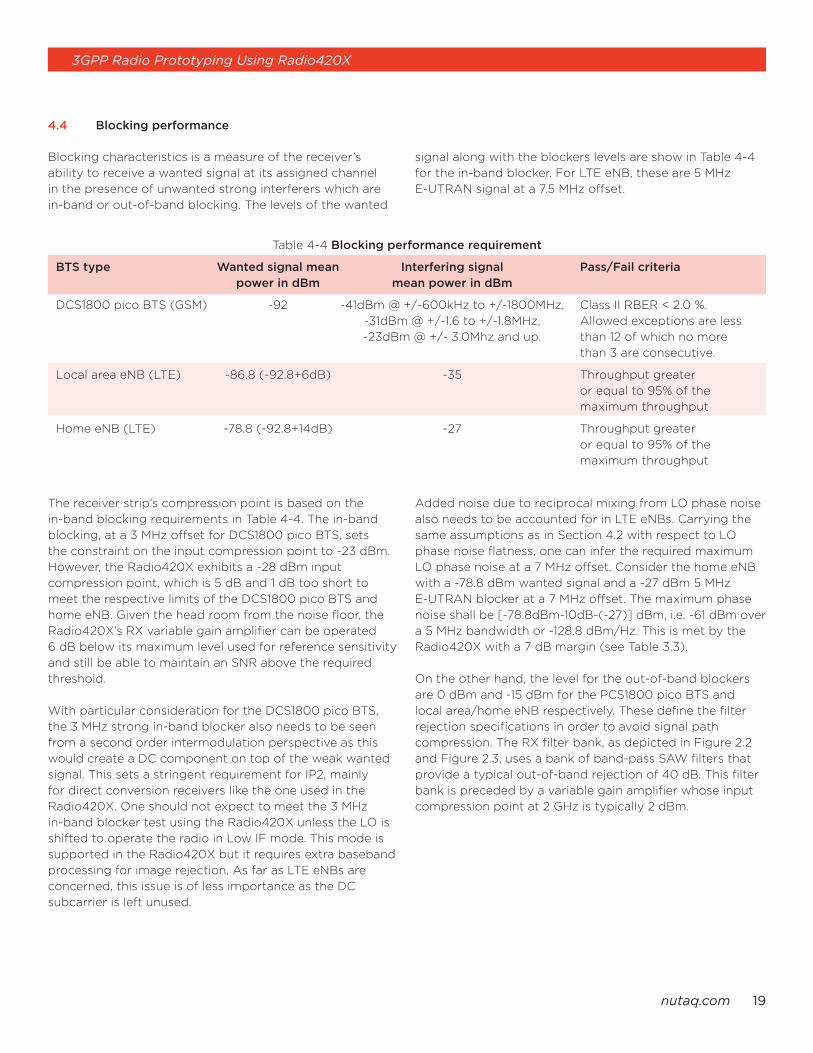
Table 4-4 Blocking.performance.requirement
. BTS.type. Wanted.signal.mean. Interfering.signal. Pass/Fail.criteria
. . power.in.dBm. mean.power.in.dBm
DCS1800 pico BTS (GSM) -92 -41dBm @ +/-600kHz to +/-1800MHz, Class II RBER < 2.0 %.
-31dBm @ +/-1.6 to +/-1.8MHz, Allowed exceptions are less
-23dBm @ +/- 3.0Mhz and up. than 12 of which no more
than 3 are consecutive.
Local area eNB (LTE) -86.8 (-92.8+6dB) -35 Throughput greater
or equal to 95% of the
maximum throughput
Home eNB (LTE) -78.8 (-92.8+14dB) -27 Throughput greater
or equal to 95% of the
maximum throughput
Blocking characteristics is a measure of the receiver’s
ability to receive a wanted signal at its assigned channel
in the presence of unwanted strong interferers which are
in-band or out-of-band blocking. The levels of the wanted
signal along with the blockers levels are show in Table 4-4
for the in-band blocker. For LTE eNB, these are 5 MHz
E-UTRAN signal at a 7.5 MHz offset.
The receiver strip’s compression point is based on the
in-band blocking requirements in Table 4-4. The in-band
blocking, at a 3 MHz offset for DCS1800 pico BTS, sets
the constraint on the input compression point to -23 dBm.
However, the Radio420X exhibits a -28 dBm input
compression point, which is 5 dB and 1 dB too short to
meet the respective limits of the DCS1800 pico BTS and
home eNB. Given the head room from the noise floor, the
Radio420X’s RX variable gain amplifier can be operated
6 dB below its maximum level used for reference sensitivity
and still be able to maintain an SNR above the required
threshold.
With particular consideration for the DCS1800 pico BTS,
the 3 MHz strong in-band blocker also needs to be seen
from a second order intermodulation perspective as this
would create a DC component on top of the weak wanted
signal. This sets a stringent requirement for IP2, mainly
for direct conversion receivers like the one used in the
Radio420X. One should not expect to meet the 3 MHz
in-band blocker test using the Radio420X unless the LO is
shifted to operate the radio in Low IF mode. This mode is
supported in the Radio420X but it requires extra baseband
processing for image rejection. As far as LTE eNBs are
concerned, this issue is of less importance as the DC
subcarrier is left unused.
Added noise due to reciprocal mixing from LO phase noise
also needs to be accounted for in LTE eNBs. Carrying the
same assumptions as in Section 4.2 with respect to LO
phase noise flatness, one can infer the required maximum
LO phase noise at a 7 MHz offset. Consider the home eNB
with a -78.8 dBm wanted signal and a -27 dBm 5 MHz
E-UTRAN blocker at a 7 MHz offset. The maximum phase
noise shall be [-78.8dBm-10dB-(-27)] dBm, i.e. -61 dBm over
a 5 MHz bandwidth or -128.8 dBm/Hz. This is met by the
Radio420X with a 7 dB margin (see Table 3.3).
On the other hand, the level for the out-of-band blockers
are 0 dBm and -15 dBm for the PCS1800 pico BTS and
local area/home eNB respectively. These define the filter
rejection specifications in order to avoid signal path
compression. The RX filter bank, as depicted in Figure 2.2
and Figure 2.3, uses a bank of band-pass SAW filters that
provide a typical out-of-band rejection of 40 dB. This filter
bank is preceded by a variable gain amplifier whose input
compression point at 2 GHz is typically 2 dBm.

3GPP Radio Prototyping Using Radio420X
20nutaq.com
This paper has addressed some of the critical radio design requirements for GSM and LTE base transceiver stations.
The requirements were mapped to frequently used radio performance metrics like compression points, intercept points,
and noise figures. When projected onto the Radio420X’s RF performance, one can easily see the potential of using the
Radio420X for 3GPP radio design and prototyping. The Radio420X can be operated at any frequency from 300 MHz to
3.8 GHz in either FDD or TDD modes. Even if it’s not very accurate, our analysis and discussion helps to educate, not only
on how to use the Radio420X for prototyping, but also to help beginner radio designers gain a better understanding on
how to interpret 3GPP radio performance specifications.
5. Conclusion
3GPP Radio Prototyping Using Radio420X
21nutaq.com
[1] 3GPP TS 45.005: “Radio transmission and reception”.
[2] 3GPP TS 36 104: “E-UTRA Base Station (BS) radio transmission and reception”.
[3] NUATQ, “1 or 2-channel, Multimode SDR 0.3–3.8 GHz RF transceivers FMC,”
(http://nutaq.com/en/products/view/+nutaq-radio420x#Documentation)
[4] M. Ahmed Ouameur, “Understanding Radio Impairments on OFDM Transmitter Performance,”
Nutaq, March 12th, 2013 (http://blog.nutaq.com/blog/understanding-radio-impairments-ofdm-transmitter-
performance).
[5] M. Ahmed Ouameur, “The Relationship between Adjacent Channel Power Ratio and IMD3 in LTE,”
Nutaq, May 9th, 2013 (http://blog.nutaq.com/blog/relationship-between-adjacent-channel-power-ratio-
and-imd3-lte).
6. References

3GPP Radio Prototyping Using Radio420X
22nutaq.com2150 Cyrille-Duquet, Quebec City (Quebec) G1N 2G3 CANADA T. 418-914-7484 | 1-855-914-7484 | F. [email protected]
Nutaq products are constantly being improved; therefore, Nutaq reserves the right to modify the information herein at any time and without notice.


