Page 1
TS 5G212 v23 (2016-9) Technical Specification
KT PyeongChang 5G Special Interest Group (KT 5G-SIG)
KT 5th Generation Radio Access
Physical Layer
Multiplexing and channel coding
(Release 1)
Ericsson Intel Corp Nokia Qualcomm Technologies Inc Samsung Electronics amp KT
Disclaimer This document provides information related to 5G technology All information provided herein is subject to change without notice The members of the KT PyeongChang 5G Special Interest Group (ldquoKT 5G-SIGrdquo) disclaim and make no guaranty or warranty express or implied as to the accuracy or completeness of any information contained or referenced herein THE KT 5G-SIG AND ITS MEMBERS DISCLAIM ANY IMPLIED WARRANTY OF MERCHANTABILITY NON-INFRINGEMENT OR FITNESS FOR ANY PARTICULAR PURPOSE AND ALL INFORMATION IS PROVIDED ON AN ldquoAS-ISrdquo BASIS No licenses under any intellectual property of any kind are provided by any person (whether a member of the KT 5G-SIG or not) that may be necessary to access or utilize any of the information contained herein including but not limited to any source materials referenced herein and any patents required to implement or develop any technology described herein It shall be the responsibility of anyone attempting to use the information contained or referenced herein to obtain any such licenses if necessary The KT 5G-SIG and its members disclaim liability for any damages or losses of any nature whatsoever whether direct indirect incidental special or consequential resulting from the use of or reliance on any information contained or referenced herein
copy 2016 KT corp All rights reserved
KT 5G-SIG
TS 5G212 v23 (2016-9) 2
Document History
Version Date Change
10 2016-02-17 First Draft Version
21 2016-07-13 Pre-final Version
22 2016-08-29 Apply CR for clarification
23 2016-09-19 Changes for technicaleditorial correction (including DCI format B1
update)
KT 5G-SIG
TS 5G212 v23 (2016-9) 3
Contents
Foreword 5
1 Scope 6
2 References 6
3 Definitions symbols and abbreviations 6
31 Definitions 6
32 Symbols 6
33 Abbreviations 6
4 Mapping to physical channels 7
41 Uplink 7
42 Downlink 7
5 Channel coding multiplexing and interleaving 7
51 Generic procedures 7
511 CRC calculation 7
512 Code block segmentation 8
513 Channel coding 10
5131 Tail biting convolutional coding 10
5132 LDPC encoder 11
514 Rate matching 16
5141 Rate matching for LDPC coded transport channels 16
5142 Rate matching for convolutionally coded transport channels and control information 17
515 Code block concatenation 19
52 Uplink transport channels and control information 20
521 Random access channel 20
522 Uplink shared channel 20
5221 Transport block CRC attachment 21
5222 Code block segmentation 21
5223 Channel coding of UL-SCH 22
5224 Rate matching 22
5225 Code block concatenation 22
5226 Channel coding of control information 22
5227 Data and control multiplexing 27
5228 Channel interleaver 27
523 Uplink control information on xPUCCH 28
5231 Channel coding for UCI HARQ-ACK 29
5232 Channel coding for UCI scheduling request 30
5233 Channel coding for UCI channel quality information 30
5234 Channel coding for UCI Beam related information feedback 31
5235 Channel coding for multiple UCIs 32
524 Uplink control information on xPUSCH without UL-SCH data 32
5241 Channel coding of control information 32
5242 Control information mapping 33
5243 Channel interleaver 33
53 Downlink transport channels and control information 33
531 Broadcast channel 33
5311 Transport block CRC attachment 34
5312 Channel coding 34
5313 Rate matching 35
531A Extended broadcast channel 35
531A1 Transport block CRC attachment 35
531A2 Channel coding 35
531A3 Rate matching 36
532 Downlink shared channel 36
5321 Transport block CRC attachment 37
5322 Code block segmentation 37
5323 Channel coding 37
KT 5G-SIG
TS 5G212 v23 (2016-9) 4
5324 Rate matching 38
5325 Code block concatenation 38
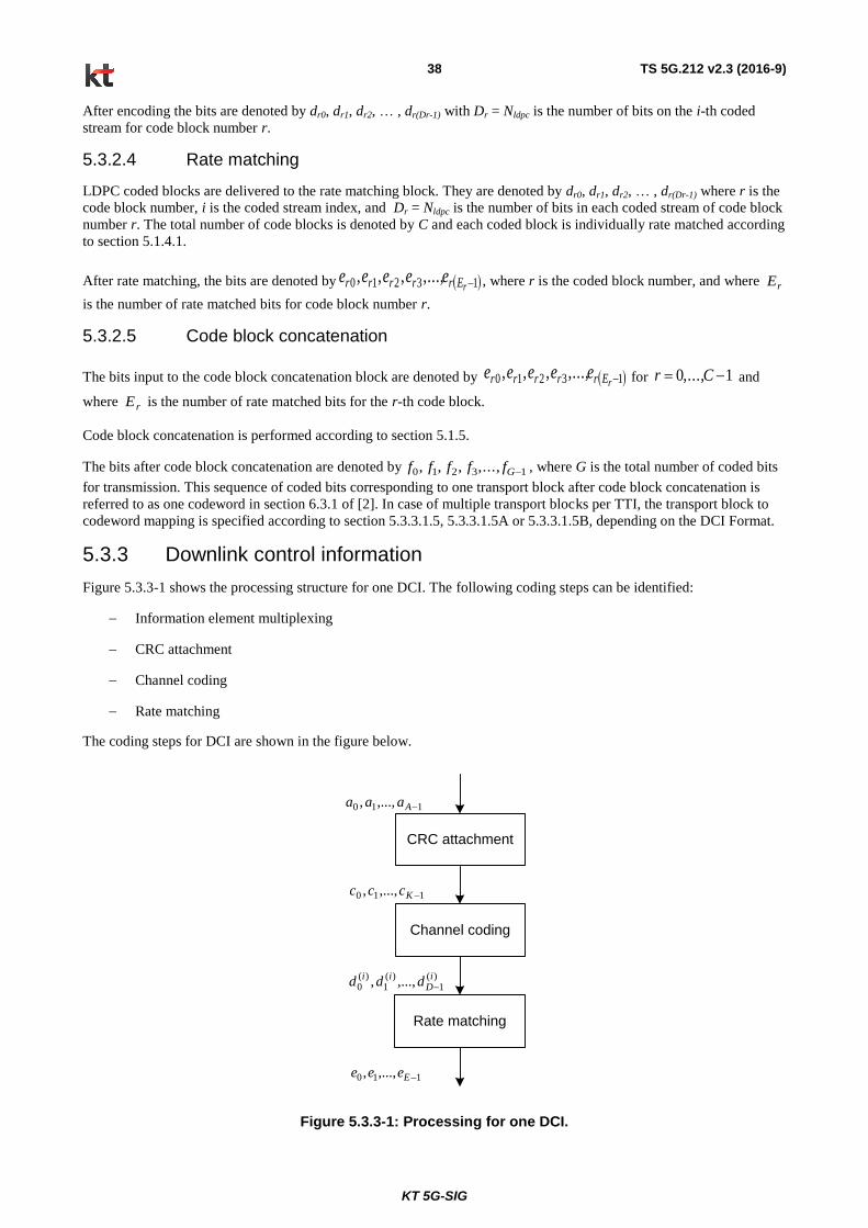
533 Downlink control information 38
5331 DCI formats 39
53311 Format A1 39
53312 Format A2 42
53313 Format B1 42
53314 Format B2 45
5332 CRC attachment 45
5333 Channel coding 45 5334 Rate matching 45
KT 5G-SIG
TS 5G212 v23 (2016-9) 5
Foreword
This Technical Specification has been produced by the KT PyeongChang 5G Special Interest Group (KT 5G-SIG)
KT 5G-SIG
TS 5G212 v23 (2016-9) 6
1 Scope
The present document specifies the coding multiplexing and mapping to physical channels for 5G Radio Access (5G
RA)
2 References
The following documents contain provisions which through reference in this text constitute provisions of the present
document
References are either specific (identified by date of publication edition number version number etc) or
non-specific
For a specific reference subsequent revisions do not apply
[1] TS 5G201 5G Radio Access (5G RA) Physical layer General description
[2] TS 5G211 5G Radio Access (5G RA) Physical channel and modulation
[3] TS 5G213 5G Radio Access (5G RA) Physical layer procedures
[4] TS 5G321 ldquo5G Radio Access (5G RA) 5G Medium Access Control Protocolrdquo
[5] TS 5G331 ldquo5G Radio Access (5G RA) 5G Radio Resource Control (5G-RRC) Protocol
Specificationrdquo
3 Definitions symbols and abbreviations
31 Definitions
32 Symbols
For the purposes of the present document the following symbols apply
33 Abbreviations
For the purposes of the present document the following abbreviations apply
BCH Broadcast channel
BQI Beam Quality Information
BRS Beam measurement Reference Signal
CP Cyclic Prefix
CSI Channel State Information
DCI Downlink Control Information
DL-SCH Downlink Shared channel
FDD Frequency Division Duplexing
LDPC Low Density Parity Check
xPBCH Physical Broadcast channel
xPDCCH Physical Downlink Control channel
xPDSCH Physical Downlink Shared channel
PMI Precoding Matrix Indicator
xPRACH Physical Random Access channel
xPUSCH Physical Uplink Shared channel
xRACH Random Access channel
RI Rank Indication
SR Scheduling Request
SRS Sounding Reference Signal
TDD Time Division Duplexing
TPMI Transmitted Precoding Matrix Indicator
KT 5G-SIG
TS 5G212 v23 (2016-9) 7
UCI Uplink Control Information
UL-SCH Uplink Shared channel
4 Mapping to physical channels
41 Uplink
Table 41-1 specifies the mapping of the uplink transport channels to their corresponding physical channels Table 41-2
specifies the mapping of the uplink control channel information to its corresponding physical channel
Table 41-1
TrCH Physical Channel
UL-SCH xPUSCH
RACH xPRACH
Table 41-2
Control information Physical Channel
UCI xPUCCH xPUSCH
42 Downlink
Table 42-1 specifies the mapping of the downlink transport channels to their corresponding physical channels Table
42-2 specifies the mapping of the downlink control channel information to its corresponding physical channel
Table 42-1
TrCH Physical Channel
DL-SCH xPDSCH
BCH xPBCH ePBCH
Table 42-2
Control information Physical Channel
DCI xPDCCH
5 Channel coding multiplexing and interleaving
Data and control streams fromto MAC layer are encoded decoded to offer transport and control services over the radio
transmission link Channel coding scheme is a combination of error detection error correcting rate matching
interleaving and transport channel or control information mapping ontosplitting from physical channels
51 Generic procedures
This section contains coding procedures which are used for more than one transport channel or control information type
511 CRC calculation
Denote the input bits to the CRC computation by 13210 Aaaaaa and the parity bits by 13210 Lppppp A
is the size of the input sequence and L is the number of parity bits The parity bits are generated by one of the following
cyclic generator polynomials
- gCRC24A(D) = [D24
+ D23
+ D18
+ D17
+ D14
+ D11
+ D10
+ D7 + D
6 + D
5 + D
4 + D
3 + D + 1] and
- gCRC16(D) = [D16
+ D12
+ D5 + 1] for a CRC length L = 16
KT 5G-SIG
TS 5G212 v23 (2016-9) 8
- gCRC8(D) = [D8 + D
7 + D
4 + D
3 + D + 1] for a CRC length of L = 8
The encoding is performed in a systematic form which means that in GF(2) the polynomial
231
2222
123
024
122
123
0 pDpDpDpDaDaDa AAA
yields a remainder equal to 0 when divided by the corresponding length-24 CRC generator polynomial gCRC24A(D) the
polynomial
151
1414
115
016
114
115
0 pDpDpDpDaDaDa AAA
yields a remainder equal to 0 when divided by gCRC16(D) and the polynomial
7
1
6
6
1
7
0
8
1
6
1
7
0 pDpDpDpDaDaDa A
AA
yields a remainder equal to 0 when divided by gCRC8(D)
The bits after CRC attachment are denoted by 13210 Bbbbbb where B = A+ L The relation between ak and bk is
kk ab for k = 0 1 2 hellip A-1
Akk pb for k = A A+1 A+2 A+L-1
512 Code block segmentation
The input bit sequence to the code block segmentation is denoted by 13210 Bbbbbb where B gt 0 If B is larger
than the maximum code block size Kmax segmentation of the input bit sequence is performed
The maximum and minimum code block sizes depending on the code rate and Coding Type are depicted in Table 512-
1
Table 512-1 Kmax and Kmin
Coding Type Code Rate Kmax Kmin
Type 1 56 1620 540
34 1458 486
23 1296 432
12 972 324
Type 2 13 1620 540
If the number of filler bits Fr calculated below is not 0 filler bits are added to r-th blocks where r is the code block
number
Note that if B lt Kmin filler bits are added to the end of the code block
The filler bits shall be set to ltNULLgt at the input to the encoder
For a given code rate total number of code blocks C is determined by
if Ble Kmax
Number of code blocks 1C
else
Number of code blocks maxΒΚC
end if
KT 5G-SIG
TS 5G212 v23 (2016-9) 9
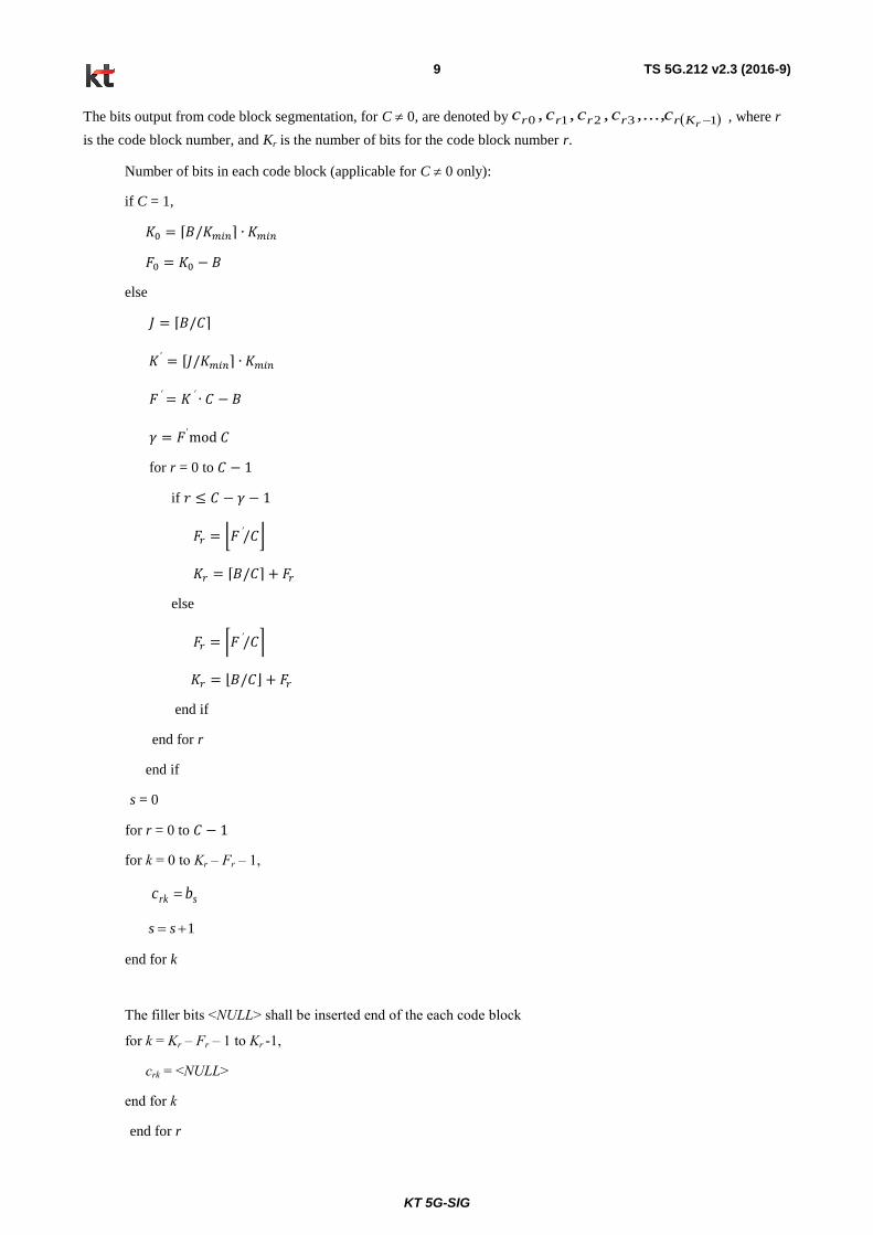
The bits output from code block segmentation for C 0 are denoted by 13210 rKrrrrr ccccc where r
is the code block number and Kr is the number of bits for the code block number r
Number of bits in each code block (applicable for C 0 only)
if C = 1
1198700 = lceil119861119870119898119894119899rceil ∙ 119870119898119894119899
1198650 = 1198700 minus 119861
else
119869 = lceil119861119862rceil
119870 prime = lceil119869119870119898119894119899rceil ∙ 119870119898119894119899
119865prime = 119870 prime ∙ 119862 minus 119861
120574 = 119865primemod 119862
for r = 0 to 119862 minus 1
if 119903 le 119862 minus 120574 minus 1
119865119903 = lfloor119865prime119862rfloor
119870119903 = lceil119861119862rceil + 119865119903
else
119865119903 = lceil119865prime119862rceil
119870119903 = lfloor119861119862rfloor + 119865119903
end if
end for r
end if
s = 0
for r = 0 to 119862 minus 1
for k = 0 to Kr ndash Fr ndash 1
srk bc
1 ss
end for k
The filler bits ltNULLgt shall be inserted end of the each code block
for k = Kr ndash Fr ndash 1 to Kr -1
crk = ltNULLgt
end for k
end for r
KT 5G-SIG
TS 5G212 v23 (2016-9) 10
513 Channel coding
The bit sequence input for a given code block to channel coding is denoted by 13210 Kccccc where K is the
number of bits to encode After encoding the bits are denoted by)(1
)(3
)(2
)(1
)(0
iD
iiiiddddd and
1D3210 ddddd for
convolutional coding scheme and LDPC coding scheme respectively where D is the number of encoded bits per output
stream and i indexes the encoder output stream The relation between kc and )(ikd and between K and D is dependent
on the channel coding scheme
The following channel coding schemes can be applied to TrCHs
- Tail biting convolutional coding
- LDPC coding
Usage of coding scheme and coding rate for the different types of TrCH is shown in Table 513-1 Usage of coding
scheme and coding rate for the different control information types is shown in Table 513-2
The values of D in connection with each coding scheme
- tail biting convolutional coding with rate 13 D = K
- LDPC coding with code rate R D = KR
The range for the output stream index i is 0 1 and 2 for tail biting convolutional coding scheme
Table 513-1 Usage of channel coding scheme and coding rate for TrCHs
TrCH Coding scheme Coding rate
UL-SCH LDPC coding variable
DL-SCH
BCH Tail biting
convolutional coding
13
Table 513-2 Usage of channel coding scheme and coding rate for control information
Control Information Coding scheme Coding rate
DCI Tail biting
convolutional coding
13
UCI
Block code variable
Tail biting convolutional
coding 13
5131 Tail biting convolutional coding
A tail biting convolutional code with constraint length 7 and coding rate 13 is defined
The configuration of the convolutional encoder is presented in Figure 5131-1
The initial value of the shift register of the encoder shall be set to the values corresponding to the last 6 information bits
in the input stream so that the initial and final states of the shift register are the same Therefore denoting the shift
register of the encoder by 5210 ssss then the initial value of the shift register shall be set to
iKi cs 1
KT 5G-SIG
TS 5G212 v23 (2016-9) 11
D D D DD D
G0 = 133 (octal)
G1 = 171 (octal)
G2 = 165 (octal)
kc
)0(kd
)1(kd
)2(kd
Figure 5131-1 Rate 13 tail biting convolutional encoder
The encoder output streams)0(
kd )1(
kd and )2(
kd correspond to the first second and third parity streams respectively
as shown in Figure 5131-1
5132 LDPC encoder
The K bits including filler bits (c0 c1 c2 hellip cK-1) are encoded based on D-K by D parity check matrix (H) where D is
number of encoded bits and D - K is the number of parity check bits The parity check bits (p0 p1 p2 hellip pD-K -1) are
obtained so that H∙ dT = 0 where d =(c0c1c2 hellip cK-1 p0 p1 p2 hellip pD-K-1) is coded bits stream
The parity check matrix H is defined as
119867 =
[
11987511988600 11987511988601 11987511988602
11987511988610 11987511988611 11987511988612
11987511988620 11987511988621 11987511988622
⋯119875
1198860119873119897119889119901119888_119887minus2 1198751198860119873119897119889119901119888_119887minus1
1198751198861119873119897119889119901119888_119887minus2 119875
1198861119873119897119889119901119888_119887minus1
1198751198862119873119897119889119901119888_119887minus2 119875
1198862119873119897119889119901119888_119887minus1
⋮ ⋱ ⋮
119875119886119873119901119886119903119894119905119910_119887minus10 119875
119886119873119901119886119903119894119905119910_119887minus11 119875119886119873119901119886119903119894119905119910_119887minus12 ⋯ 119875
119886119873119901119886119903119894119905119910_119887minus1119873119897119889119901119888_119887minus2 119875119886119873119901119886119903119894119905119910_119887minus1119873119897119889119901119888_119887minus1]
where Paij (0leiltNparity_b 0lejltNldpc_b) is cyclic-permutation matrix obtained from the zero matrix and the Z by Z identity
matrix by cyclically shifted the columns to the right by aij elements The value of Z is shift size obtained by Z =lceil119870119870119898119894119899rceil ∙ 27 where Kmin is given in Table 512-1
The matrix Paij is Z by Z zero matrix when aij is -1 The codeword length D information length K and number of parity
bits D-K is equal to Nldpc_b x Z Kldpc_b x Z and Npairty_b x Z respectively The parameters Nldpc_b Kldpc_b and Nparity_b
according to code rates are depicted in Table 5132-1
Table 5132-1 Parameters of parity check matrix
Coding Type Code Rate Nldpc_b Kldpc_b Nparity_b
Type 1
56 24 20 4
34 24 18 6
23 24 16 8
12 24 12 12
Type 2 13 60 20 40
For Type 1 the parity check matrix is obtained based on Tables 5132-2 5132-3 5132-4 and 5132-5 which
show the exponents (aij) of parity check matrix when the code rate equals 56 34 23 and 12 for each encoded bits
respectively
For Type 2 the parity check matrix is obtained based on Table 5132-6 which shows the exponents (aij) of parity check
matrix when the Z equals 81 The set of exponents (aij) are used to determine the exponents for all other code length of
the same code rate Z=27 or 54 The exponents aij(Z) for code size corresponding to shift size Z determined above are
derived from aij by using a modulo function as below
0mod
0
ijij
ijij
ij aifZa
aifaZa
KT 5G-SIG
TS 5G212 v23 (2016-9) 12
Table 5132-2 Matrix exponents for Code rate R=56 Type 1
(a) D = 648 bits Z=27 bits
17 13 8 21 9 3 18 12 10 0 4 15 19 2 5 10 26 19 13 13 1 0 -1 -1
3 12 11 14 11 25 5 18 0 9 2 26 26 10 24 7 14 20 4 2 -1 0 0 -1
22 16 4 3 10 21 12 5 21 14 19 5 -1 8 5 18 11 5 5 15 0 -1 0 0
7 7 14 14 4 16 16 24 24 10 1 7 15 6 10 26 8 18 21 14 1 -1 -1 0
(b) D = 1296 bits Z=54 bits
48 29 37 52 2 16 6 14 53 31 34 5 18 42 53 31 45 -1 46 52 1 0 -1 -1
17 4 30 7 43 11 24 6 14 21 6 39 17 40 47 7 15 41 19 -1 -1 0 0 -1
7 2 51 31 46 23 16 11 53 40 10 7 46 53 33 35 -1 25 35 38 0 -1 0 0
19 48 41 1 10 7 36 47 5 29 52 52 31 10 26 6 3 2 -1 51 1 -1 -1 0
(c) D = 1944 bits Z=81 bits
13 48 80 66 4 74 7 30 76 52 37 60 -1 49 73 31 74 73 23 -1 1 0 -1 -1
69 63 74 56 64 77 57 65 6 16 51 -1 64 -1 68 9 48 62 54 27 -1 0 0 -1
51 15 0 80 24 25 42 54 44 71 71 9 67 35 -1 58 -1 29 -1 53 0 -1 0 0
16 29 36 41 44 56 59 37 50 24 -1 65 4 65 52 -1 4 -1 73 52 1 -1 -1 0
Table 5132-3 Matrix exponents for R=34 Type 1
(a) D = 648 bits Z=27 bits
16 17 22 24 9 3 14 -1 4 2 7 -1 26 -1 2 -1 21 -1 1 0 -1 -1 -1 -1
25 12 12 3 3 26 6 21 -1 15 22 -1 15 -1 4 -1 -1 16 -1 0 0 -1 -1 -1
25 18 26 16 22 23 9 -1 0 -1 4 -1 4 -1 8 23 11 -1 -1 -1 0 0 -1 -1
9 7 0 1 17 -1 -1 7 3 -1 3 23 -1 16 -1 -1 21 -1 0 -1 -1 0 0 -1
24 5 26 7 1 -1 -1 15 24 15 -1 8 -1 13 -1 13 -1 11 -1 -1 -1 -1 0 0
2 2 19 14 24 1 15 19 -1 21 -1 2 -1 24 -1 3 -1 2 1 -1 -1 -1 -1 0
(b) D = 1296 bits Z=54 bits
39 40 51 41 3 29 8 36 -1 14 -1 6 -1 33 -1 11 -1 4 1 0 -1 -1 -1 -1
48 21 47 9 48 35 51 -1 38 -1 28 -1 34 -1 50 -1 50 -1 -1 0 0 -1 -1 -1
30 39 28 42 50 39 5 17 -1 6 -1 18 -1 20 -1 15 -1 40 -1 -1 0 0 -1 -1
29 0 1 43 36 30 47 -1 49 -1 47 -1 3 -1 35 -1 34 -1 0 -1 -1 0 0 -1
1 32 11 23 10 44 12 7 -1 48 -1 4 -1 9 -1 17 -1 16 -1 -1 -1 -1 0 0
13 7 15 47 23 16 47 -1 43 -1 29 -1 52 -1 2 -1 53 -1 1 -1 -1 -1 -1 0
KT 5G-SIG
TS 5G212 v23 (2016-9) 13
(c) D = 1944 bits Z=81 bits
48 29 28 39 9 61 -1 -1 -1 63 45 80 -1 -1 -1 37 32 22 1 0 -1 -1 -1 -1
4 49 42 48 11 30 -1 -1 -1 49 17 41 37 15 -1 54 -1 -1 -1 0 0 -1 -1 -1
35 76 78 51 37 35 21 -1 17 64 -1 -1 -1 59 7 -1 -1 32 -1 -1 0 0 -1 -1
9 65 44 9 54 56 73 34 42 -1 -1 -1 35 -1 -1 -1 46 39 0 -1 -1 0 0 -1
3 62 7 80 68 26 -1 80 55 -1 36 -1 26 -1 9 -1 72 -1 -1 -1 -1 -1 0 0
26 75 33 21 69 59 3 38 -1 -1 -1 35 -1 62 36 26 -1 -1 1 -1 -1 -1 -1 0
Table 5132-4 Matrix exponents for R=23 Type 1
(a) D = 648 bits Z=27 bits
25 26 14 -1 20 -1 2 -1 4 -1 -1 8 -1 16 -1 18 1 0 -1 -1 -1 -1 -1 -1
10 9 15 11 -1 0 -1 1 -1 -1 18 -1 8 -1 10 -1 -1 0 0 -1 -1 -1 -1 -1
16 2 20 26 21 -1 6 -1 1 26 -1 7 -1 -1 -1 -1 -1 -1 0 0 -1 -1 -1 -1
10 13 5 0 -1 3 -1 7 -1 -1 26 -1 -1 13 -1 16 -1 -1 -1 0 0 -1 -1 -1
23 14 24 -1 12 -1 19 -1 17 -1 -1 -1 20 -1 21 -1 0 -1 -1 -1 0 0 -1 -1
6 22 9 20 -1 25 -1 17 -1 8 -1 14 -1 18 -1 -1 -1 -1 -1 -1 -1 0 0 -1
14 23 21 11 20 -1 24 -1 18 -1 19 -1 -1 -1 -1 22 -1 -1 -1 -1 -1 -1 0 0
17 11 11 20 -1 21 -1 26 -1 3 -1 -1 18 -1 26 -1 1 -1 -1 -1 -1 -1 -1 0
(b) D = 1296 bits Z=54 bits
39 31 22 43 -1 40 4 -1 11 -1 -1 50 -1 -1 -1 6 1 0 -1 -1 -1 -1 -1 -1
25 52 41 2 6 -1 14 -1 34 -1 -1 -1 24 -1 37 -1 -1 0 0 -1 -1 -1 -1 -1
43 31 29 0 21 -1 28 -1 -1 2 -1 -1 7 -1 17 -1 -1 -1 0 0 -1 -1 -1 -1
20 33 48 -1 4 13 -1 26 -1 -1 22 -1 -1 46 42 -1 -1 -1 -1 0 0 -1 -1 -1
45 7 18 51 12 25 -1 -1 -1 50 -1 -1 5 -1 -1 -1 0 -1 -1 -1 0 0 -1 -1
35 40 32 16 5 -1 -1 18 -1 -1 43 51 -1 32 -1 -1 -1 -1 -1 -1 -1 0 0 -1
9 24 13 22 28 -1 -1 37 -1 -1 25 -1 -1 52 -1 13 -1 -1 -1 -1 -1 -1 0 0
32 22 4 21 16 -1 -1 -1 27 28 -1 38 -1 -1 -1 8 1 -1 -1 -1 -1 -1 -1 0
(c) D = 1944 bits Z=81 bits
61 75 4 63 56 -1 -1 -1 -1 -1 -1 8 -1 2 17 25 1 0 -1 -1 -1 -1 -1 -1
56 74 77 20 -1 -1 -1 64 24 4 67 -1 7 -1 -1 -1 -1 0 0 -1 -1 -1 -1 -1
28 21 68 10 7 14 65 -1 -1 -1 23 -1 -1 -1 75 -1 -1 -1 0 0 -1 -1 -1 -1
48 38 43 78 76 -1 -1 -1 -1 5 36 -1 15 72 -1 -1 -1 -1 -1 0 0 -1 -1 -1
40 2 53 25 -1 52 62 -1 20 -1 -1 44 -1 -1 -1 -1 0 -1 -1 -1 0 0 -1 -1
69 23 64 10 22 -1 21 -1 -1 -1 -1 -1 68 23 29 -1 -1 -1 -1 -1 -1 0 0 -1
12 0 68 20 55 61 -1 40 -1 -1 -1 52 -1 -1 -1 44 -1 -1 -1 -1 -1 -1 0 0
58 8 34 64 78 -1 -1 11 78 24 -1 -1 -1 -1 -1 58 1 -1 -1 -1 -1 -1 -1 0
KT 5G-SIG
TS 5G212 v23 (2016-9) 14
Table 5132-5 Matrix exponents for R=12 Type 1
(a) D = 648 bits Z=27 bits
0 -1 -1 -1 0 0 -1 -1 0 -1 -1 0 1 0 -1 -1 -1 -1 -1 -1 -1 -1 -1 -1
22 0 -1 -1 17 -1 0 0 12 -1 -1 -1 -1 0 0 -1 -1 -1 -1 -1 -1 -1 -1 -1
6 -1 0 -1 10 -1 -1 -1 24 -1 0 -1 -1 -1 0 0 -1 -1 -1 -1 -1 -1 -1 -1
2 -1 -1 0 20 -1 -1 -1 25 0 -1 -1 -1 -1 -1 0 0 -1 -1 -1 -1 -1 -1 -1
23 -1 -1 -1 3 -1 -1 -1 0 -1 9 11 -1 -1 -1 -1 0 0 -1 -1 -1 -1 -1 -1
24 -1 23 1 17 -1 3 -1 10 -1 -1 -1 -1 -1 -1 -1 -1 0 0 -1 -1 -1 -1 -1
25 -1 -1 -1 8 -1 -1 -1 7 18 -1 -1 0 -1 -1 -1 -1 -1 0 0 -1 -1 -1 -1
13 24 -1 -1 0 -1 8 -1 6 -1 -1 -1 -1 -1 -1 -1 -1 -1 -1 0 0 -1 -1 -1
7 20 -1 16 22 10 -1 -1 23 -1 -1 -1 -1 -1 -1 -1 -1 -1 -1 -1 0 0 -1 -1
11 -1 -1 -1 19 -1 -1 -1 13 -1 3 17 -1 -1 -1 -1 -1 -1 -1 -1 -1 0 0 -1
25 -1 8 -1 23 18 -1 14 9 -1 -1 -1 -1 -1 -1 -1 -1 -1 -1 -1 -1 -1 0 0
3 -1 -1 -1 16 -1 -1 2 25 5 -1 -1 1 -1 -1 -1 -1 -1 -1 -1 -1 -1 -1 0
(b) D = 1296 bits Z=54 bits
40 -1 -1 -1 22 -1 49 23 43 -1 -1 -1 1 0 -1 -1 -1 -1 -1 -1 -1 -1 -1 -1
50 1 -1 -1 48 35 -1 -1 13 -1 30 -1 -1 0 0 -1 -1 -1 -1 -1 -1 -1 -1 -1
39 50 -1 -1 4 -1 2 -1 -1 -1 -1 49 -1 -1 0 0 -1 -1 -1 -1 -1 -1 -1 -1
33 -1 -1 38 37 -1 -1 4 1 -1 -1 -1 -1 -1 -1 0 0 -1 -1 -1 -1 -1 -1 -1
45 -1 -1 -1 0 22 -1 -1 20 42 -1 -1 -1 -1 -1 -1 0 0 -1 -1 -1 -1 -1 -1
51 -1 -1 48 35 -1 -1 -1 44 -1 18 -1 -1 -1 -1 -1 -1 0 0 -1 -1 -1 -1 -1
47 11 -1 -1 -1 17 -1 -1 51 -1 -1 -1 0 -1 -1 -1 -1 -1 0 0 -1 -1 -1 -1
5 -1 25 -1 6 -1 45 -1 13 40 -1 -1 -1 -1 -1 -1 -1 -1 -1 0 0 -1 -1 -1
33 -1 -1 34 24 -1 -1 -1 23 -1 -1 46 -1 -1 -1 -1 -1 -1 -1 -1 0 0 -1 -1
1 -1 27 -1 1 -1 -1 -1 38 -1 44 -1 -1 -1 -1 -1 -1 -1 -1 -1 -1 0 0 -1
-1 18 -1 -1 23 -1 -1 8 0 35 -1 -1 -1 -1 -1 -1 -1 -1 -1 -1 -1 -1 0 0
49 -1 17 -1 30 -1 -1 -1 34 -1 -1 19 1 -1 -1 -1 -1 -1 -1 -1 -1 -1 -1 0
(c) D = 1944 bits Z=81 bits
57 -1 -1 -1 50 -1 11 -1 50 -1 79 -1 1 0 -1 -1 -1 -1 -1 -1 -1 -1 -1 -1
3 -1 28 -1 0 -1 -1 -1 55 7 -1 -1 -1 0 0 -1 -1 -1 -1 -1 -1 -1 -1 -1
30 -1 -1 -1 24 37 -1 -1 56 14 -1 -1 -1 -1 0 0 -1 -1 -1 -1 -1 -1 -1 -1
62 53 -1 -1 53 -1 -1 3 35 -1 -1 -1 -1 -1 -1 0 0 -1 -1 -1 -1 -1 -1 -1
40 -1 -1 20 66 -1 -1 22 28 -1 -1 -1 -1 -1 -1 -1 0 0 -1 -1 -1 -1 -1 -1
0 -1 -1 -1 8 -1 42 -1 50 -1 -1 8 -1 -1 -1 -1 -1 0 0 -1 -1 -1 -1 -1
69 79 79 -1 -1 -1 56 -1 52 -1 -1 -1 0 -1 -1 -1 -1 -1 0 0 -1 -1 -1 -1
KT 5G-SIG
TS 5G212 v23 (2016-9) 15
65 -1 -1 -1 38 57 -1 -1 72 -1 27 -1 -1 -1 -1 -1 -1 -1 -1 0 0 -1 -1 -1
64 -1 -1 -1 14 52 -1 -1 30 -1 -1 32 -1 -1 -1 -1 -1 -1 -1 -1 0 0 -1 -1
-1 45 -1 70 0 -1 -1 -1 77 9 -1 -1 -1 -1 -1 -1 -1 -1 -1 -1 -1 0 0 -1
2 56 -1 57 35 -1 -1 -1 -1 -1 12 -1 -1 -1 -1 -1 -1 -1 -1 -1 -1 -1 0 0
24 -1 61 -1 60 -1 -1 27 51 -1 -1 16 1 -1 -1 -1 -1 -1 -1 -1 -1 -1 -1 0
Table 5132-6 Matrix exponents for R=13 Z = 81 bits Type 2
54 19 24 68 12 2 18 16 13 46 66 52 21 9 -1 80 24 -1 3 11 1 0 -1 -1 -1 -1 -1 -1 -1 -1 -1 -1 -1 -1
-1 -1 -1 -1 -1 -1 -1 -1 -1 -1 -1 -1 -1 -1 -1 -1 -1 -1 -1 -1 -1 -1 -1 -1 -1 -1
10 76 29 30 8 28 16 35 62 53 57 53 15 38 72 73 -1 45 38 71 -1 0 0 -1 -1 -1 -1 -1 -1 -1 -1 -1 -1 -1
-1 -1 -1 -1 -1 -1 -1 -1 -1 -1 -1 -1 -1 -1 -1 -1 -1 -1 -1 -1 -1 -1 -1 -1 -1 -1
70 71 31 35 20 21 6 56 36 52 22 37 50 27 58 16 56 41 -1 -1 0 -1 0 0 -1 -1 -1 -1 -1 -1 -1 -1 -1 -1
-1 -1 -1 -1 -1 -1 -1 -1 -1 -1 -1 -1 -1 -1 -1 -1 -1 -1 -1 -1 -1 -1 -1 -1 -1 -1
41 24 25 49 28 6 28 60 22 70 11 27 1 -1 67 -1 22 78 76 5 1 -1 -1 0 -1 -1 -1 -1 -1 -1 -1 -1 -1 -1
-1 -1 -1 -1 -1 -1 -1 -1 -1 -1 -1 -1 -1 -1 -1 -1 -1 -1 -1 -1 -1 -1 -1 -1 -1 -1
27 70 45 45 28 9 29 30 39 29 56 80 29 -1 -1 -1 -1 -1 -1 -1 -1 -1 -1 -1 0 -1 -1 -1 -1 -1 -1 -1 -1 -1
-1 -1 -1 -1 -1 -1 -1 -1 -1 -1 -1 -1 -1 -1 -1 -1 -1 -1 -1 -1 -1 -1 -1 -1 -1 -1
-1 77 8 69 49 68 78 -1 66 8 6 79 40 -1 -1 -1 -1 -1 -1 -1 -1 -1 -1 -1 -1 0 -1 -1 -1 -1 -1 -1 -1 -1
-1 -1 -1 -1 -1 -1 -1 -1 -1 -1 -1 -1 -1 -1 -1 -1 -1 -1 -1 -1 -1 -1 -1 -1 -1 -1
74 37 -1 41 6 -1 -1 -1 -1 57 63 -1 -1 -1 -1 -1 56 -1 -1 -1 -1 -1 -1 -1 -1 -1 0 -1 -1 -1 -1 -1 -1 -1
-1 -1 -1 -1 -1 -1 -1 -1 -1 -1 -1 -1 -1 -1 -1 -1 -1 -1 -1 -1 -1 -1 -1 -1 -1 -1
-1 -1 24 -1 -1 16 74 27 44 -1 -1 42 12 -1 -1 -1 -1 -1 -1 -1 -1 -1 -1 -1 -1 -1 -1 0 -1 -1 -1 -1 -1 -1
-1 -1 -1 -1 -1 -1 -1 -1 -1 -1 -1 -1 -1 -1 -1 -1 -1 -1 -1 -1 -1 -1 -1 -1 -1 -1
-1 9 20 -1 25 -1 -1 -1 -1 18 3 59 -1 -1 -1 -1 -1 -1 -1 -1 -1 -1 -1 -1 -1 -1 -1 -1 0 -1 -1 -1 -1 -1
-1 -1 -1 -1 -1 -1 -1 -1 -1 -1 -1 -1 -1 -1 -1 -1 -1 -1 -1 -1 -1 -1 -1 -1 -1 -1
-1 -1 -1 79 -1 5 78 -1 1 -1 -1 -1 22 -1 -1 -1 -1 -1 -1 -1 -1 -1 27 -1 -1 -1 -1 -1 -1 0 -1 -1 -1 -1
-1 -1 -1 -1 -1 -1 -1 -1 -1 -1 -1 -1 -1 -1 -1 -1 -1 -1 -1 -1 -1 -1 -1 -1 -1 -1
-1 24 47 -1 -1 67 30 -1 -1 -1 -1 43 -1 -1 18 -1 -1 42 -1 -1 -1 -1 -1 -1 -1 -1 -1 -1 -1 -1 0 -1 -1 -1
-1 -1 -1 -1 -1 -1 -1 -1 -1 -1 -1 -1 -1 -1 -1 -1 -1 -1 -1 -1 -1 -1 -1 -1 -1 -1
-1 -1 -1 -1 78 -1 -1 -1 58 51 70 -1 35 -1 -1 -1 -1 -1 -1 -1 -1 -1 64 -1 -1 -1 -1 -1 -1 -1 -1 0 -1 -1
-1 -1 -1 -1 -1 -1 -1 -1 -1 -1 -1 -1 -1 -1 -1 -1 -1 -1 -1 -1 -1 -1 -1 -1 -1 -1
-1 0 -1 -1 78 -1 39 -1 66 38 -1 -1 -1 -1 4 -1 -1 -1 -1 -1 -1 63 -1 -1 -1 -1 -1 -1 -1 -1 -1 -1 0 -1
-1 -1 -1 -1 -1 -1 -1 -1 -1 -1 -1 -1 -1 -1 -1 -1 -1 -1 -1 -1 -1 -1 -1 -1 -1 -1
-1 -1 45 -1 -1 3 -1 -1 -1 -1 12 11 38 -1 -1 -1 -1 80 -1 -1 -1 -1 -1 -1 -1 -1 -1 -1 -1 -1 -1 -1 -1 0
-1 -1 -1 -1 -1 -1 -1 -1 -1 -1 -1 -1 -1 -1 -1 -1 -1 -1 -1 -1 -1 -1 -1 -1 -1 -1
-1 -1 62 -1 57 12 -1 -1 26 -1 -1 -1 -1 -1 -1 -1 -1 -1 -1 27 35 -1 -1 -1 -1 -1 -1 -1 -1 -1 -1 -1 -1 -1
0 -1 -1 -1 -1 -1 -1 -1 -1 -1 -1 -1 -1 -1 -1 -1 -1 -1 -1 -1 -1 -1 -1 -1 -1 -1
-1 29 -1 -1 -1 -1 34 -1 -1 23 -1 51 3 -1 -1 -1 -1 -1 -1 -1 -1 -1 -1 -1 -1 -1 -1 -1 -1 -1 -1 -1 -1 -1
-1 0 -1 -1 -1 -1 -1 -1 -1 -1 -1 -1 -1 -1 -1 -1 -1 -1 -1 -1 -1 -1 -1 -1 -1 -1
-1 -1 48 -1 -1 -1 -1 -1 44 -1 -1 -1 54 -1 -1 -1 -1 71 -1 61 -1 -1 -1 -1 -1 -1 -1 -1 -1 -1 -1 -1 -1 -1
-1 -1 0 -1 -1 -1 -1 -1 -1 -1 -1 -1 -1 -1 -1 -1 -1 -1 -1 -1 -1 -1 -1 -1 -1 -1
-1 -1 -1 -1 7 -1 33 -1 -1 28 -1 -1 -1 -1 2 -1 -1 -1 -1 -1 -1 -1 -1 -1 -1 -1 -1 -1 -1 -1 -1 -1 -1 -1
-1 -1 -1 0 -1 -1 -1 -1 -1 -1 -1 -1 -1 -1 -1 -1 -1 -1 -1 -1 -1 -1 -1 -1 -1 -1
-1 48 -1 11 -1 -1 -1 -1 -1 -1 64 42 -1 -1 -1 -1 -1 -1 -1 -1 -1 -1 -1 -1 -1 -1 -1 -1 -1 -1 -1 -1 -1 -1
-1 -1 -1 -1 0 -1 -1 -1 -1 -1 -1 -1 -1 -1 -1 -1 -1 -1 -1 -1 -1 -1 -1 -1 -1 -1
KT 5G-SIG
TS 5G212 v23 (2016-9) 16
-1 -1 -1 -1 -1 73 -1 -1 -1 -1 -1 -1 -1 73 -1 -1 -1 -1 -1 -1 77 -1 37 -1 -1 -1 -1 -1 -1 -1 -1 -1 -1 -1
-1 -1 -1 -1 -1 0 -1 -1 -1 -1 -1 -1 -1 -1 -1 -1 -1 -1 -1 -1 -1 -1 -1 -1 -1 -1
-1 45 -1 -1 -1 -1 -1 -1 -1 40 -1 56 -1 -1 -1 -1 -1 -1 -1 -1 -1 -1 65 -1 -1 -1 -1 -1 -1 -1 -1 -1 -1 -1
-1 -1 -1 -1 -1 -1 0 -1 -1 -1 -1 -1 -1 -1 -1 -1 -1 -1 -1 -1 -1 -1 -1 -1 -1 -1
-1 -1 51 -1 -1 -1 12 -1 -1 -1 40 -1 -1 -1 -1 -1 -1 -1 -1 -1 41 -1 -1 -1 -1 -1 -1 -1 -1 -1 -1 -1 -1 -1
-1 -1 -1 -1 -1 -1 -1 0 -1 -1 -1 -1 -1 -1 -1 -1 -1 -1 -1 -1 -1 -1 -1 -1 -1 -1
-1 -1 -1 -1 53 5 -1 -1 77 -1 -1 -1 -1 -1 -1 -1 -1 -1 39 -1 -1 -1 -1 -1 -1 -1 -1 -1 -1 -1 -1 -1 -1 -1
-1 -1 -1 -1 -1 -1 -1 -1 0 -1 -1 -1 -1 -1 -1 -1 -1 -1 -1 -1 -1 -1 -1 -1 -1 -1
-1 -1 -1 -1 -1 -1 -1 -1 -1 -1 -1 -1 68 -1 52 -1 11 57 -1 -1 -1 -1 -1 -1 -1 -1 -1 -1 -1 -1 -1 -1 -1 -1
-1 -1 -1 -1 -1 -1 -1 -1 -1 0 -1 -1 -1 -1 -1 -1 -1 -1 -1 -1 -1 -1 -1 -1 -1 -1
-1 -1 -1 -1 -1 -1 -1 -1 66 -1 -1 32 -1 -1 -1 -1 -1 60 -1 -1 -1 29 -1 -1 -1 -1 -1 -1 -1 -1 -1 -1 -1 -1
-1 -1 -1 -1 -1 -1 -1 -1 -1 -1 0 -1 -1 -1 -1 -1 -1 -1 -1 -1 -1 -1 -1 -1 -1 -1
-1 -1 -1 -1 22 -1 -1 -1 -1 -1 9 -1 -1 -1 28 -1 -1 -1 -1 -1 -1 -1 -1 -1 -1 -1 -1 -1 -1 -1 -1 -1 -1 -1
-1 -1 -1 -1 -1 -1 -1 -1 -1 -1 -1 0 -1 -1 -1 -1 -1 -1 -1 -1 -1 -1 -1 -1 -1 -1
58 -1 -1 -1 -1 71 -1 -1 -1 -1 -1 -1 42 -1 -1 -1 -1 -1 -1 -1 -1 -1 -1 -1 -1 -1 -1 -1 -1 -1 -1 -1 -1 -1
-1 -1 -1 -1 -1 -1 -1 -1 -1 -1 -1 -1 0 -1 -1 -1 -1 -1 -1 -1 -1 -1 -1 -1 -1 -1
-1 8 75 -1 -1 -1 -1 -1 -1 -1 -1 -1 -1 43 -1 -1 -1 -1 -1 -1 -1 -1 -1 -1 -1 -1 -1 -1 -1 -1 -1 -1 -1 -1
-1 -1 -1 -1 -1 -1 -1 -1 -1 -1 -1 -1 -1 0 -1 -1 -1 -1 -1 -1 -1 -1 -1 -1 -1 -1
-1 -1 -1 -1 -1 -1 -1 -1 -1 32 -1 18 -1 -1 -1 -1 -1 -1 -1 1 -1 -1 76 -1 -1 -1 -1 -1 -1 -1 -1 -1 -1 -1
-1 -1 -1 -1 -1 -1 -1 -1 -1 -1 -1 -1 -1 -1 0 -1 -1 -1 -1 -1 -1 -1 -1 -1 -1 -1
-1 53 -1 -1 -1 -1 -1 -1 41 -1 -1 -1 -1 -1 -1 -1 -1 42 -1 -1 15 -1 -1 -1 -1 -1 -1 -1 -1 -1 -1 -1 -1 -1
-1 -1 -1 -1 -1 -1 -1 -1 -1 -1 -1 -1 -1 -1 -1 0 -1 -1 -1 -1 -1 -1 -1 -1 -1 -1
-1 -1 -1 -1 -1 -1 -1 -1 -1 -1 -1 -1 15 -1 10 -1 44 -1 4 -1 -1 -1 -1 -1 -1 -1 -1 -1 -1 -1 -1 -1 -1 -1
-1 -1 -1 -1 -1 -1 -1 -1 -1 -1 -1 -1 -1 -1 -1 -1 0 -1 -1 -1 -1 -1 -1 -1 -1 -1
-1 -1 59 -1 -1 42 18 -1 -1 -1 -1 -1 -1 -1 -1 -1 -1 -1 -1 -1 -1 -1 -1 -1 -1 -1 -1 -1 -1 -1 -1 -1 -1 -1
-1 -1 -1 -1 -1 -1 -1 -1 -1 -1 -1 -1 -1 -1 -1 -1 -1 0 -1 -1 -1 -1 -1 -1 -1 -1
52 12 -1 -1 -1 -1 49 -1 74 -1 -1 -1 -1 -1 -1 -1 -1 -1 -1 -1 -1 -1 -1 -1 -1 -1 -1 -1 -1 -1 -1 -1 -1 -1
-1 -1 -1 -1 -1 -1 -1 -1 -1 -1 -1 -1 -1 -1 -1 -1 -1 -1 0 -1 -1 -1 -1 -1 -1 -1
-1 -1 39 -1 -1 -1 -1 -1 -1 38 18 -1 21 -1 -1 -1 -1 -1 -1 -1 -1 -1 -1 -1 -1 -1 -1 -1 -1 -1 -1 -1 -1 -1
-1 -1 -1 -1 -1 -1 -1 -1 -1 -1 -1 -1 -1 -1 -1 -1 -1 -1 -1 0 -1 -1 -1 -1 -1 -1
-1 -1 -1 -1 47 -1 -1 -1 -1 -1 -1 -1 -1 14 -1 -1 -1 -1 -1 -1 -1 18 48 -1 -1 -1 -1 -1 -1 -1 -1 -1 -1 -1
-1 -1 -1 -1 -1 -1 -1 -1 -1 -1 -1 -1 -1 -1 -1 -1 -1 -1 -1 -1 0 -1 -1 -1 -1 -1
-1 -1 -1 -1 -1 31 -1 -1 -1 -1 -1 31 -1 -1 -1 -1 17 -1 49 -1 -1 -1 -1 -1 -1 -1 -1 -1 -1 -1 -1 -1 -1 -1
-1 -1 -1 -1 -1 -1 -1 -1 -1 -1 -1 -1 -1 -1 -1 -1 -1 -1 -1 -1 -1 0 -1 -1 -1 -1
-1 26 -1 -1 -1 -1 -1 -1 -1 -1 -1 14 -1 -1 -1 -1 1 4 -1 -1 -1 -1 -1 -1 -1 -1 -1 -1 -1 -1 -1 -1 -1 -1
-1 -1 -1 -1 -1 -1 -1 -1 -1 -1 -1 -1 -1 -1 -1 -1 -1 -1 -1 -1 -1 -1 0 -1 -1 -1
-1 -1 -1 -1 -1 -1 14 -1 -1 65 -1 -1 2 -1 -1 77 -1 -1 -1 -1 -1 -1 -1 -1 -1 -1 -1 -1 -1 -1 -1 -1 -1 -1
-1 -1 -1 -1 -1 -1 -1 -1 -1 -1 -1 -1 -1 -1 -1 -1 -1 -1 -1 -1 -1 -1 -1 0 -1 -1
-1 -1 -1 -1 -1 -1 -1 -1 -1 -1 37 -1 -1 -1 53 -1 -1 -1 -1 -1 74 -1 -1 -1 -1 -1 -1 -1 -1 -1 -1 -1 -1 -1
-1 -1 -1 -1 -1 -1 -1 -1 -1 -1 -1 -1 -1 -1 -1 -1 -1 -1 -1 -1 -1 -1 -1 -1 0 -1
-1 -1 37 -1 -1 -1 -1 -1 50 -1 -1 -1 -1 -1 -1 -1 -1 -1 -1 -1 -1 -1 16 -1 -1 -1 -1 -1 -1 -1 -1 -1 -1 -1
-1 -1 -1 -1 -1 -1 -1 -1 -1 -1 -1 -1 -1 -1 -1 -1 -1 -1 -1 -1 -1 -1 -1 -1 -1 0
514 Rate matching
5141 Rate matching for LDPC coded transport channels
The rate matching for LDPC coded transport channels is defined per coded bit stream dk The sequence of bits ek for
transmission is generated according to below
KT 5G-SIG
TS 5G212 v23 (2016-9) 17
Denoting by E the rate matching output sequence length for the r-th coded block the rate matching output bit sequence
is ke k = 01 1E
Define by G the total number of bits available for the transmission of one transport block
Set mL QNGG where Qm is equal to 2 for QPSK 4 for 16QAM and 6 for 64QAM and where NL is equal to the
number of layers a transport block is mapped onto Note that for the case of transmit diversity transmission mode NL =
1
Set CG mod where C is the number of code blocks computed in section 512
if 119903 lt 120574
set 119864 = 119873119871 ∙ 119876119898 ∙ lceil119866prime119862rceil
else
set 119864 = 119873119871 ∙ 119876119898 ∙ lfloor119866prime119862rfloor
end if
For Coding Type 1 set 00 k
For Coding Type 2 set 1198960 = (lceil119863
4rceil ∙ 119903119907119894119889119909) where rvidx =0 1 2 or 3
Set k = 0 and j = 0
while k lt E
if 119889(1198960+119895) mod 119863 nelt 119873119880119871119871 gt
119890119896 = 119889(1198960+119895) mod 119863
k = k +1
end if
j = j +1
end while
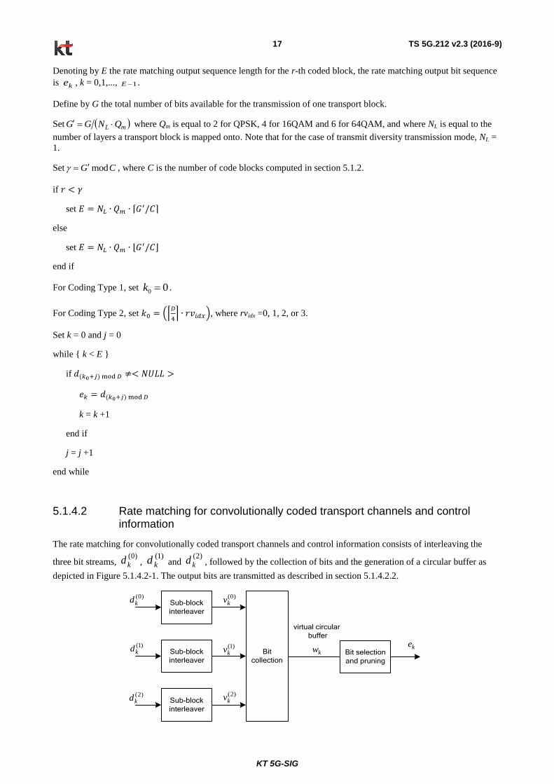
5142 Rate matching for convolutionally coded transport channels and control information
The rate matching for convolutionally coded transport channels and control information consists of interleaving the
three bit streams )0(
kd )1(
kd and )2(
kd followed by the collection of bits and the generation of a circular buffer as
depicted in Figure 5142-1 The output bits are transmitted as described in section 51422
Sub-block
interleaver
Sub-block
interleaver
Sub-block
interleaver
Bit
collection
virtual circular
buffer
Bit selection
and pruning
)0(kd
)1(kd
)2(kd
ke
)0(kv
)1(kv
)2(kv
kw
KT 5G-SIG
TS 5G212 v23 (2016-9) 18
Figure 5142-1 Rate matching for convolutionally coded transport channels and control information
The bit stream )0(
kd is interleaved according to the sub-block interleaver defined in section 51421 with an output
sequence defined as )0(
1
)0(2
)0(1
)0(0
Kvvvv and where K is defined in section 51421
The bit stream )1(
kd is interleaved according to the sub-block interleaver defined in section 51421 with an output
sequence defined as)1(
1
)1(2
)1(1
)1(0
Kvvvv
The bit stream )2(
kd is interleaved according to the sub-block interleaver defined in section 51421 with an output
sequence defined as)2(
1
)2(2
)2(1
)2(0
Kvvvv
The sequence of bits ke for transmission is generated according to section 51422
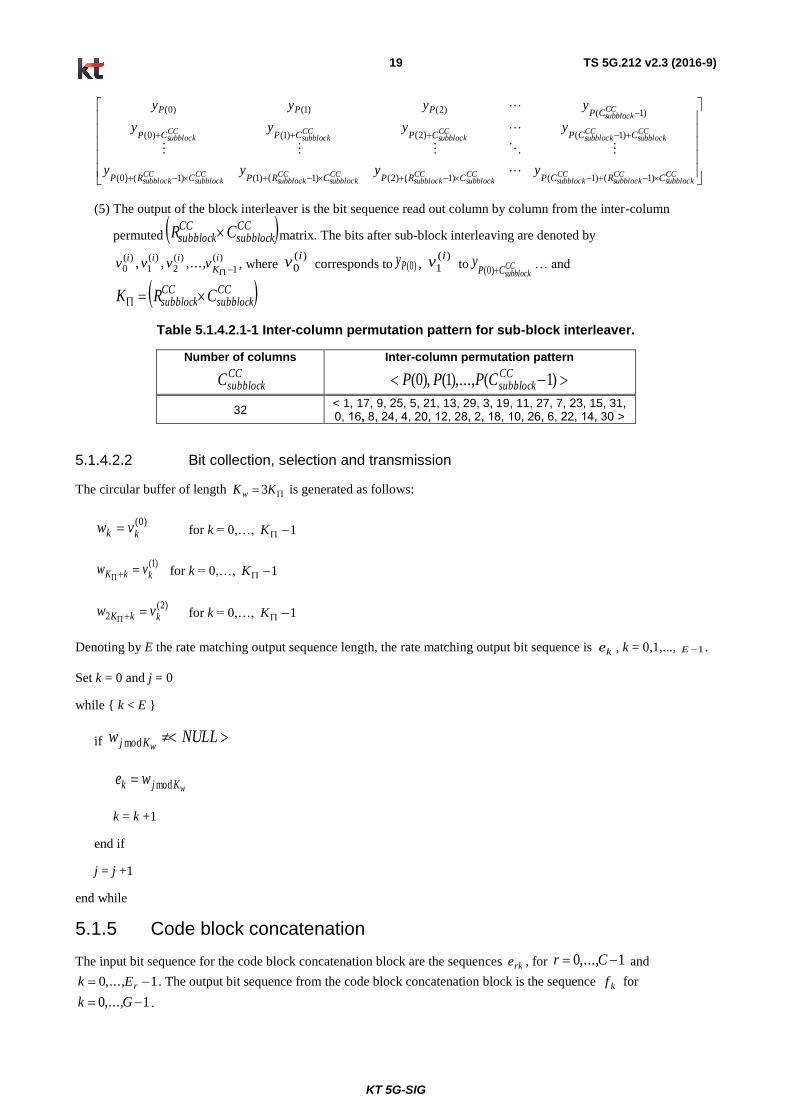
51421 Sub-block interleaver
The bits input to the block interleaver are denoted by)(1
)(2
)(1
)(0
iD
iiidddd where D is the number of bits The output
bit sequence from the block interleaver is derived as follows
(1) Assign 32CCsubblockC to be the number of columns of the matrix The columns of the matrix are numbered 0 1
2hellip 1CCsubblockC from left to right
(2) Determine the number of rows of the matrixCCsubblockR by finding minimum integer
CCsubblockR such that
CCsubblock
CCsubblock CRD
The rows of rectangular matrix are numbered 0 1 2hellip 1CC
subblockR from top to bottom
(3) If DCR CCsubblock
CCsubblock then DCRN CC
subblockCCsubblockD dummy bits are padded such that yk = ltNULLgt
for k = 0 1hellip ND - 1 Then )(i
kkN dyD
k = 0 1hellip D-1 and the bit sequence yk is written into the
CCsubblock
CCsubblock CR matrix row by row starting with bit y0 in column 0 of row 0
)1(2)1(1)1()1(
1221
1210
CCsubblock
CCsubblock
CCsubblock
CCsubblock
CCsubblock
CCsubblock
CCsubblock
CCsubblock
CCsubblock
CCsubblock
CCsubblock
CCsubblock
CCsubblock
CRCRCRCR
CCCC
C
yyyy
yyyy
yyyy
(4) Perform the inter-column permutation for the matrix based on the pattern 110 CCsubblockCj
jP that is shown
in table 51421-1 where P(j) is the original column position of the j-th permuted column After permutation of
the columns the inter-column permuted CCsubblock
CCsubblock CR matrix is equal to
KT 5G-SIG
TS 5G212 v23 (2016-9) 19
CCsubblock
CCsubblock
CCsubblock
CCsubblock
CCsubblock
CCsubblock
CCsubblock
CCsubblock
CCsubblock
CCsubblock
CCsubblock
CCsubblock
CCsubblock
CCsubblock
CCsubblock
CRCPCRPCRPCRP
CCPCPCPCP
CPPPP
yyyy
yyyy
yyyy
)1()1()1()2()1()1()1()0(
)1()2()1()0(
)1()2()1()0(
(5) The output of the block interleaver is the bit sequence read out column by column from the inter-column
permuted CCsubblock
CCsubblock CR matrix The bits after sub-block interleaving are denoted by
)(
1
)(2
)(1
)(0
i
K
iiivvvv
where
)(0i
v corresponds to )0(Py )(
1i
v to CCsubblockCP
y)0(
hellip and
CCsubblock
CCsubblock CRK
Table 51421-1 Inter-column permutation pattern for sub-block interleaver
Number of columns
CCsubblockC
Inter-column permutation pattern
)1()1()0( CCsubblockCPPP
32 lt 1 17 9 25 5 21 13 29 3 19 11 27 7 23 15 31 0 16 8 24 4 20 12 28 2 18 10 26 6 22 14 30 gt
51422 Bit collection selection and transmission
The circular buffer of length KKw 3 is generated as follows
)0(
kk vw for k = 0hellip 1K
)1(
kkK vw for k = 0hellip 1K
)2(
2 kkK vw for k = 0hellip 1K
Denoting by E the rate matching output sequence length the rate matching output bit sequence is ke k = 01 1E
Set k = 0 and j = 0
while k lt E
if NULLwwKj mod
wKjk we mod
k = k +1
end if
j = j +1
end while
515 Code block concatenation
The input bit sequence for the code block concatenation block are the sequences rke for 10 Cr and
10 rEk The output bit sequence from the code block concatenation block is the sequence kf for
10 Gk
KT 5G-SIG
TS 5G212 v23 (2016-9) 20
The code block concatenation consists of sequentially concatenating the rate matching outputs for the different code
blocks Therefore
Set 0k and 0r
while Cr
Set 0j
while rEj
rjk ef
1 kk
1 jj
end while
1 rr
end while
52 Uplink transport channels and control information
521 Random access channel
The sequence index for the random access channel is received from higher layers and is processed according to [2]
522 Uplink shared channel
The processing structure for the UL-SCH transport channel on one UL cell
Add CRC to the transport block
Code block segmentation
Channel coding of data and control information
Rate matching
Code block concatenation
Multiplexing of data and control information
Channel interleaver
The coding steps for one UL-SCH transport block are shown in the figure below The same general processing applies
for each UL-SCH transport block
KT 5G-SIG
TS 5G212 v23 (2016-9) 21
Code block segmentation
Channel coding
Transport blockCRC attachment
1B10 bbb
Rate matching
Data and Control multiplexing
Channel Interleaver
1A10 aaa
)1( Krrr1r0 ccc
)1( Drrr1r0 ddd
)1( Errr1r0 eee
1G10 fff
Code blockConcatenation
1
0 1 Hg g g
ChannelCoding
ChannelCoding
][ )1( O10 ooo
1 CQIL QN10 qqq
][110
RI
O
RIRIRIooo
1
RI
RI RI RI
0 1 Qq q q
1 RIL QNH10 hhh
Figure 522-1 Transport block processing for UL-SCH
5221 Transport block CRC attachment
Error detection is provided on each UL-SCH transport block through a Cyclic Redundancy Check (CRC)
The entire transport block is used to calculate the CRC parity bits Denote the bits in a transport block delivered to layer
1 by 13210 Aaaaaa and the parity bits by 13210 Lppppp A is the size of the transport block and L is the
number of parity bits The lowest order information bit a0 is mapped to the most significant bit of the transport block as
defined in section 611 of [4]
The parity bits are computed and attached to the UL-SCH transport block according to section 511 setting L to 24 bits
and using the generator polynomial gCRC24A(D)
5222 Code block segmentation
The bits input to the code block segmentation are denoted by 13210 Bbbbbb where B is the number of bits in the
transport block (including CRC)
KT 5G-SIG
TS 5G212 v23 (2016-9) 22
The bits after code block segmentation are denoted by 13210 rKrrrrr ccccc where r is the code block number
and Kr is the number of bits for code block number r
5223 Channel coding of UL-SCH
Code blocks are delivered to the channel coding block The bits in a code block are denoted by
13210 rKrrrrr ccccc where r is the code block number and Kr is the number of bits in code block number r
The total number of code blocks is denoted by C and each code block is individually LDPC encoded according to
section 5132
After encoding the bits are denoted by dr0 dr1 dr2 hellip dr(Dr-1) with Dr = Nldpc is the number of bits on the i-th coded
stream for code block number r
5224 Rate matching
LDPC coded blocks are delivered to the rate matching block They are denoted by dr0 dr1 dr2 hellip dr(Dr-1) where r is the
code block number i is the coded stream index and Dr = Nldpc is the number of bits in each coded stream of code block
number r The total number of code blocks is denoted by C and each coded block is individually rate matched according
to section 5141 After rate matching the bits are denoted by 13210 rErrrrr eeeee where r is the coded block
number and where rE is the number of rate matched bits for code block number r
5225 Code block concatenation
The bits input to the code block concatenation block are denoted by 13210 rErrrrr eeeee for 10 Cr and
where rE is the number of rate matched bits for the r-th code block
Code block concatenation is performed according to section 515
The bits after code block concatenation are denoted by 13210 Gfffff where G is the total number of coded bits
for transmission of the given transport block over LN transmission layers excluding the bits used for control
transmission when control information is multiplexed with the UL-SCH transmission Note that for the case of transmit
diversity transmission mode NL = 1
5226 Channel coding of control information
Control data arrives at the coding unit in the form of channel quality information (CQI andor PMI andor beam state
information (BSI) andor beam refinement information (BRI)) and rank indication Different coding rates for the
control information are achieved by allocating different number of coded symbols for its transmission When control
data are transmitted in the xPUSCH the channel coding for rank indication and channel quality and beam related
information 1210 Ooooo is done independently
When the UE transmits rank indicator bits it shall determine the number of coded modulation symbols per layer Q for
rank indicator bits as follows
Only one transport block is transmitted in the xPUSCH conveying rank indicator bits
1
0
min
xPUSCH initial xPUSCH initial xPUSCH
sc symb offset xPUSCH xPUSCH
sc symbC
rr
O M NQ M N
K
where
- O is the number of rank indicator bits and
KT 5G-SIG
TS 5G212 v23 (2016-9) 23
- xPUSCH
scM is the scheduled bandwidth for xPUSCH transmission in the current sub-frame for the transport block
expressed as a number of subcarriers in [2] where a number of subcarriers used for PCRS transmission are not
counted and
- xPUSCH
symbN is the number of OFDM symbols per subframe for xPUSCH in the current sub-frame for the transport
block respectively where symbol(s) that DMRS is mapped on is not counted
- xPUSCH
symb
initial-xPUSCH
symb NN xPUSCH
sc
initialxPUSCH
sc MM C and rK are obtained from the initial xPDCCH
for the same transport block If there is no initial xPDCCH for the same transport block C and rK shall be
determined from
- the random access response grant for the same transport block when the xPUSCH is initiated by the random
access response grant
For rank indication QQQ mRI and
RI
offset
xPUSCH
offset where mQ is the modulation order of a given transport
block and RI
offset shall be determined according to [3]
For rank indication (RI)
-If RI feedback consists of 1-bit of information ie ][ 0RIo it is first encoded according to Table 5226-1 The
][ 0RIo to RI mapping is given by Table 5226-2
Table 5226-1 Encoding of 1-bit RI
Qm Encoded RI
2 y] [ 0
RIo
4 y x x] [ 0
RIo
6 ]y x x x x [ 0
RIo
Table 5226-2 RIo0 to RI mapping
RIo0 RI
0 1
1 2
The ldquoxrdquo and ldquoyrdquo in Table 5226-1 is placeholders for [2] to scramble the RI bits in a way that maximizes the Euclidean
distance of the modulation symbols carrying rank information
For the case where RI feedback consists of one or two bits of information the bit sequence RIQ
RIRIRI
RIqqqq
1210
is
obtained by concatenation of multiple encoded RI blocks where RIQ is the total number of coded bits for all the
encoded RI blocks The last concatenation of the encoded RI block may be partial so that the total bit sequence length
is equal to RIQ
When rank information is to be multiplexed with UL-SCH at a given xPUSCH the rank information is multiplexed in
all layers of all transport blocks of that xPUSCH For a given transport block the vector sequence output of the channel
coding for rank information is denoted by RI
Q
RIRI
RIqqq
110
where
RI
iq 10 RIQi are column vectors of
length Lm NQ and where mRIRI QQQ The vector sequence is obtained as follows
Set i j k to 0
while RIQi
KT 5G-SIG
TS 5G212 v23 (2016-9) 24
] [ˆ1
RIQi
RIi
RI
k mqqq -- temporary row vector
ˆ ˆ[ ]
LN
RI RI RI T
k k kq q q
644474448L -- replicating the row vector
RI
kq NL times and transposing into a column vector
mQii
1 kk
end while
where LN is the number of layers onto which the UL-SCH transport block is mapped Note that for the case of
transmit diversity transmission mode NL = 1
For channel quality control information (CQI andor PMI andor BSI andor BRI denoted as CQIPMIBSIBRI)
When the UE transmits channel quality control information bits it shall determine the number of modulation coded
symbols per layer Q for channel quality and beam related information as
1
0
( )min
xPUSCH initial xPUSCH initial xPUSCH
sc symb offset xPUSCH xPUSCH RIsc symbC
mr
r
O L M N QQ M N
QK
where
- O is the number of CQIPMIBSIBRI bits and
- L is the number of CRC bits given by
otherwise8
110 OL and
- CQI m
Q QQ and CQI
offset
xPUSCH
offset where CQI
offset shall be determined according to [3] depending on the
number of transmission codewords for the corresponding xPUSCH
- If RI is not transmitted then 0RIQ
xPUSCH initial
symbN xPUSCH initial
scM C and rK are obtained from the xPDCCH for the same transport block If there is no
xPDCCH for the same transport block xPUSCH initial
scM C and rK shall be determined from
- the random access response grant for the same transport block when the xPUSCH is initiated by the random
access response grant
For UL-SCH data information xPUSCH xPUSCH
symb scL m CQI RIG N N M Q Q Q where
- LN is the number of layers the corresponding UL-SCH transport block is mapped onto note that for the case of
transmit diversity transmission mode NL = 1 and
- xPUSCH
scM is the scheduled bandwidth for xPUSCH transmission in the current sub-frame for the transport block
where the subcarriers used for PCRS transmission are not counted and
- xPUSCH
symbN is the number of OFDM symbols in the current xPUSCH transmission sub-frame block obtained from
the xPDCCH for the same transport block where symbol(s) that DMRS is mapped on are not counted
If the CQIPMIBSIBRI payload size is less than or equal to 11 bits the channel coding of the channel quality and
beam related information is performed according to section 52263 with input sequence 1210 Ooooo where any
CQIPMI bits occur at the beginning of the input sequence followed by any BSI bits followed by any BRI bits
KT 5G-SIG
TS 5G212 v23 (2016-9) 25
For CQIPMIBSIBRI payload sizes greater than 11 bits the CRC attachment channel coding and rate matching of the
channel quality and beam related information is performed according to sections 511 5131 and 5142 respectively
The input bit sequence to the CRC attachment operation is 1210 Ooooo where any CQIPMI bits occur at the
beginning of the input sequence followed by any BSI bits followed by any BRI bits The output bit sequence of the
CRC attachment operation is the input bit sequence to the channel coding operation The output bit sequence of the
channel coding operation is the input bit sequence to the rate matching operation
The output sequence for the channel coding of channel quality and beam related information is denoted by
13210 CQIL QNqqqqq where LN is the number of layers the corresponding UL-SCH transport block is mapped
onto Note that for the case of transmit diversity transmission mode NL = 1
52261 Channel quality information formats for wideband CQI reports
Table 52261-1 shows the fields and the corresponding bit widths for the channel quality information feedback for
wideband reports for xPDSCH transmissions
Table 52261-1 Fields for channel quality information feedback for one wideband CQI report
Field Bit width
Rank = 1 Rank = 2 No PMI
Wideband CQI 4 4 4
Precoding matrix indicator (PMI) 248 248 0
Rank indication (RI) 1 1 0
The bit width of PMI depends on the number of the corresponding CSI-RS port for 248 Tx ports the bit width of PMI
is equal to 2 bits 4bits and 8bits respectively
52262 Beam related information formats for wideband reports
Table 52262-1 shows the fields and the corresponding bit widths for the beam state information feedback for
wideband report for xPDSCH transmissions
Table 52262-1 Fields for BSI feedback for wideband report
Field Bit width
BRS index 9N
Wide-band BRSRP 7N
Table 52262-2 shows the fields and the corresponding bit widths for the beam refinement information feedback for
wideband report for xPDSCH transmissions
Table 52262-2 Fields for BRI feedback for one wideband report
Field Bit width
BRRS index 3N
Wide-band BRRS-RP 7N
The beam related information in Table 52262-1 and Table 52262-2 form the bit sequence 1210 Ooooo with
0o corresponding to the first bit of the first field in the table 1o corresponding to the second bit of the first field in the
table and 1Oo corresponding to the last bit in the last field in the table The first bit of each field corresponds to MSB
and the last bit LSB
KT 5G-SIG
TS 5G212 v23 (2016-9) 26
52263 Channel coding for CQIPMIBSIBRI information in xPUSCH
The channel quality andor beam related information bits input to the channel coding block are denoted by
13210 Oooooo where O is the number of bits The number of channel quality and beam related information bits
depend on the transmission format When xPUCCH-based reporting format is used the number of CQIPMIBSIBRI
bits is defined in section 52331 for wideband reports When xPUSCH-based reporting format is used the number of
CQIPMIBSIBRI bits is defined in section 52261 for wideband reports
The channel quality andor beam related information is first coded using a (32 O) block code The code words of the
(32 O) block code are a linear combination of the 11 basis sequences denoted Min and defined in Table 52263-1
Table 52263-1 Basis sequences for (32 O) code
i Mi0 Mi1 Mi2 Mi3 Mi4 Mi5 Mi6 Mi7 Mi8 Mi9 Mi10
0 1 1 0 0 0 0 0 0 0 0 1
1 1 1 1 0 0 0 0 0 0 1 1
2 1 0 0 1 0 0 1 0 1 1 1
3 1 0 1 1 0 0 0 0 1 0 1
4 1 1 1 1 0 0 0 1 0 0 1
5 1 1 0 0 1 0 1 1 1 0 1
6 1 0 1 0 1 0 1 0 1 1 1
7 1 0 0 1 1 0 0 1 1 0 1
8 1 1 0 1 1 0 0 1 0 1 1
9 1 0 1 1 1 0 1 0 0 1 1
10 1 0 1 0 0 1 1 1 0 1 1
11 1 1 1 0 0 1 1 0 1 0 1
12 1 0 0 1 0 1 0 1 1 1 1
13 1 1 0 1 0 1 0 1 0 1 1
14 1 0 0 0 1 1 0 1 0 0 1
15 1 1 0 0 1 1 1 1 0 1 1
16 1 1 1 0 1 1 1 0 0 1 0
17 1 0 0 1 1 1 0 0 1 0 0
18 1 1 0 1 1 1 1 1 0 0 0
19 1 0 0 0 0 1 1 0 0 0 0
20 1 0 1 0 0 0 1 0 0 0 1
21 1 1 0 1 0 0 0 0 0 1 1
22 1 0 0 0 1 0 0 1 1 0 1
23 1 1 1 0 1 0 0 0 1 1 1
24 1 1 1 1 1 0 1 1 1 1 0
25 1 1 0 0 0 1 1 1 0 0 1
26 1 0 1 1 0 1 0 0 1 1 0
27 1 1 1 1 0 1 0 1 1 1 0
28 1 0 1 0 1 1 1 0 1 0 0
29 1 0 1 1 1 1 1 1 1 0 0
30 1 1 1 1 1 1 1 1 1 1 1
31 1 0 0 0 0 0 0 0 0 0 0
The encoded CQIPMIBSIBRI block is denoted by 13210 Bbbbbb where 32B and
1
0
2modO
n
nini Mob where i = 0 1 2 hellip B-1
The output bit sequence 0 1 2 3 1
L CQIN Qq q q q q is obtained by circular repetition of the encoded CQIPMIBSIBRI
block as follows
Bii bq mod where i = 0 1 2 hellip NLQCQI-1 where NL is the number of layers the corresponding UL-SCH
transport block is mapped onto Note that for the case of transmit diversity transmission mode NL = 1
KT 5G-SIG
TS 5G212 v23 (2016-9) 27
5227 Data and control multiplexing
The control and data multiplexing is performed such that the multiplexing ensures control and data information are
mapped to different modulation symbols
The inputs to the data and control multiplexing are the coded bits of the control information denoted by
13210 CQIL QNqqqqq where mCQICQI QQQ and the coded bits of the UL-SCH denoted by
13210 Gfffff The output of the data and control multiplexing operation is denoted by 13210
H
ggggg
where CQIL QNGH and mL QNHH and wherei
g 10 Hi are column vectors of length
Lm NQ H is the total number of coded bits allocated for UL-SCH data and CQIPMIBSIBRI information across
the LN transmission layers of the transport block Note that for the case of transmit diversity transmission mode NL = 1
In the case of single transport block transmission and assuming that LN is the number of layers onto which the UL-
SCH transport block is mapped (NL = 1 for transmit diversity transmission) the control information and the data shall
be multiplexed as follows
Set i j k to 0
while CQIL QNj -- first place the control information
TQNjjk mL
qqg ] [1
mL QNjj
1 kk
end while
while Gi -- then place the data
TNQiik Lm
ffg ] [ 1
Lm NQii
1 kk
end while
5228 Channel interleaver
The channel interleaver described in this section in conjunction with the resource element mapping for xPUSCH in [2]
implements a time-first mapping of control modulation symbols and frequency-first mapping of data modulation
symbols onto the transmit waveform
The inputs to the channel interleaver are denoted by 1210
H
gggg andRI
Q
RIRIRI
RIqqqq
1210
The number of modulation symbols per layer in the subframe is given by total RIH H Q The output bit sequence
from the channel interleaver is derived as follows
(1) Assign PUSCHsymbNCmux to be the number of columns of the matrix The columns of the matrix are numbered 0
1 2hellip 1muxC from left to right PUSCHsymbN is determined according to section 5226
KT 5G-SIG
TS 5G212 v23 (2016-9) 28
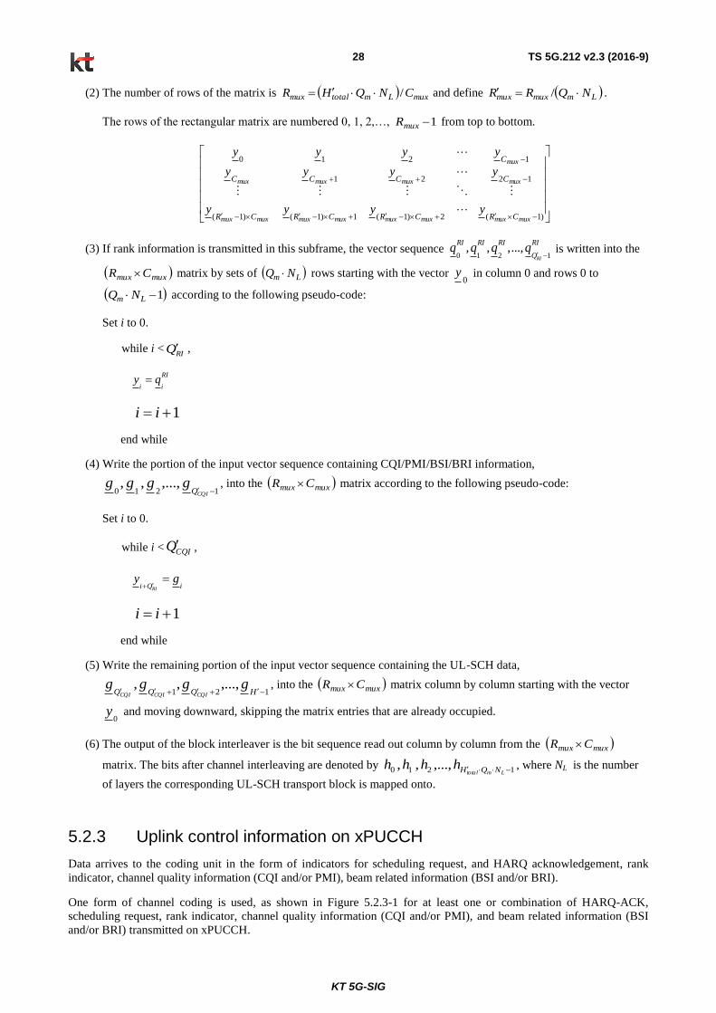
(2) The number of rows of the matrix is muxLmtotalmux CNQHR and define Lmmuxmux NQRR
The rows of the rectangular matrix are numbered 0 1 2hellip 1muxR from top to bottom
)1(2)1(1)1()1(
1221
1210
muxmuxmuxmuxmuxmuxmuxmux
muxmuxmuxmux
mux
CRCRCRCR
CCCC
C
yyyy
yyyy
yyyy
(3) If rank information is transmitted in this subframe the vector sequence 0 1 2 1
RI
RI RI RI RI
Qq q q q
is written into the
muxmux CR matrix by sets of Lm NQ rows starting with the vector 0
y in column 0 and rows 0 to
1 Lm NQ according to the following pseudo-code
Set i to 0
while i ltRIQ
RI
i iy q
1 ii
end while
(4) Write the portion of the input vector sequence containing CQIPMIBSIBRI information
1210
CQIQgggg into the muxmux CR matrix according to the following pseudo-code
Set i to 0
while i lt CQIQ
RIi Q i
y g
1 ii
end while
(5) Write the remaining portion of the input vector sequence containing the UL-SCH data
121
HQQQgggg
CQICQICQI
into the muxmux CR matrix column by column starting with the vector
0y and moving downward skipping the matrix entries that are already occupied
(6) The output of the block interleaver is the bit sequence read out column by column from the muxmux CR
matrix The bits after channel interleaving are denoted by 1210 Lmtotal NQHhhhh where NL is the number
of layers the corresponding UL-SCH transport block is mapped onto
523 Uplink control information on xPUCCH
Data arrives to the coding unit in the form of indicators for scheduling request and HARQ acknowledgement rank
indicator channel quality information (CQI andor PMI) beam related information (BSI andor BRI)
One form of channel coding is used as shown in Figure 523-1 for at least one or combination of HARQ-ACK
scheduling request rank indicator channel quality information (CQI andor PMI) and beam related information (BSI
andor BRI) transmitted on xPUCCH
KT 5G-SIG
TS 5G212 v23 (2016-9) 29
110 Aaaa
110 Bbbb
Channel coding
Figure 523-1 Processing for UCI
5231 Channel coding for UCI HARQ-ACK
The HARQ-ACK bits are received from higher layers for each subframe HARQ-ACK consists of 1-bit of information
ie 0b corresponding to ACKNACK bit for codeword 0 Each positive acknowledgement (ACK) is encoded as a
binary lsquo1rsquo and each negative acknowledgement (NACK) is encoded as a binary lsquo0rsquo For the case where xPUCCH format
2 [2] is scheduled [3] the HARQ-ACK feedback consists of the concatenation of HARQ-ACK bits which the UE needs
to feedback for downlink subframes For all cells single codeword transmission modes 1 bit of HARQ-ACK
information ka is used The HARQ-ACK bits are processed for transmission according to section 111 [3]
Define 2format xPUCCH
NAN as the number of HARQ-ACK bits when xPUCCH format 2 is used for transmission of HARQ-
ACK feedback (section 111 in [3])
The sequence of bits 1210 2format xPUCCH
NAN
aaaa is obtained from the HARQ-ACK bits for different downlink
subframes
Define DL
cB as the number of downlink subframes for which the UE needs to feedback HARQ-ACK bits in cell c as
defined in Section 73 of [3]
The number of HARQ-ACK bits for the UE to convey is computed as follows
Set k = 0 ndash counter of HARQ-ACK bits
set l = 0 ndash counter of downlink subframes
while l lt DL
cB
k = k + 1
l = l+1
end while
For 102format xPUCCH
NAN the bit sequence 1210 2format xPUCCH
NAN
aaaa is obtained by setting ACK
i ia o
The sequence of bits 1210 2format xPUCCH
NAN
aaaa is encoded as follows
1
0
2format xPUCCH
2mod~ NAN
n
nini Mab
KT 5G-SIG
TS 5G212 v23 (2016-9) 30
where i = 0 1 2 hellip 31 and the basis sequences niM are defined in Table 52263-1
The output bit sequence 1210 Bbbbb is obtained by circular repetition of the sequence 31210
~
~
~
~bbbb
32mod
~ii bb
where i = 0 1 2 hellip B-1 and where RB
sc8 NB
5232 Channel coding for UCI scheduling request
The scheduling request indication is received from higher layers and is processed according to [2] and [3]
5233 Channel coding for UCI channel quality information
The channel quality information bits input to the channel coding block are denoted by 13210 Aaaaaa where A
is the number of bits The number of channel quality information bits depends on the transmission format as indicated
in section 52331 for wideband reports
For the channel quality information bits 13210 Aaaaaa if A le 11 channel coding defined in section 5231
shall be applied The output bit sequence 1210 Bbbbb where RB
sc8 NB is obtained after the channel coding
For 11 lt A le 22 the bit sequence 13210 Aaaaaa is obtained by setting 2i ia o if i is even and
2 ( 1)2 iA ia o
if i is odd The sequences of bits 0 1 2 2 1
A
a a a a
and 12 2 1 2 2 AA A A
a a a a are
encoded as follows
2 1
0
mod 2A
i n i n
n
b a M
and
2 1
20
mod2A A
i i nA nn
b a M
where i = 0 1 2 hellip 31 and the basis sequences niM are defined in Table 52263-1
The output bit sequence 1210 Bbbbb where RB
sc8 NB is obtained by the alternate concatenation of the bit
sequences 31210
~
~
~
~bbbb and 31210
~~
~~
~~
~~bbbb as follows
Set i j = 0
while RB
sc8 Ni
32mod
~ji bb 32mod11
~ ji bb
32mod2
~~ji bb 32mod13
~~ ji bb
i = i + 4
j = j + 2
KT 5G-SIG
TS 5G212 v23 (2016-9) 31
end while
52331 Channel quality information formats for wideband reports
Table 52331-1 shows the fields and the corresponding bit widths for the channel quality information feedback for
wideband reports for xPDSCH transmissions
Table 52331-1 Fields for channel quality information feedback for one wideband CQI report
Field Bit width
Rank = 1 Rank = 2 No PMI
Wideband CQI 4 4 4
Precoding matrix indicator (PMI) 248 248 0
Rank indication (RI) 1 1 0
The bit width of precoding matrix depends on the number of the corresponding CSI-RS port for 248 Tx ports the bit
width of PMI is equal to 2 bits 4bits and 8bits respectively
The channel quality bits in Table 52331-1 form the bit sequence 13210 Aaaaaa with 0a corresponding to the
first bit of the first field in each of the tables 1a corresponding to the second bit of the first field in each of the tables
and 1Aa corresponding to the last bit in the last field in each of the tables The first bit corresponds to MSB and the
last bit LSB
5234 Channel coding for UCI Beam related information feedback
The beam related information bits input to the channel coding block are denoted by 13210 Aaaaaa where A is
the number of bits The number of beam related information bits depends on the transmission format as indicated in
section 52341 for wideband reports
For the beam related information (BSI or BRI) bits 13210 Aaaaaa if A le11 then channel coding defined in
Section 5231 shall be applied The output bit sequence 1210 Bbbbb where RB
sc8 NB is obtained after the
channel coding Otherwise channel coding defined in section 5233 shall be applied and the output bit sequence
1210 Bbbbb where RB
sc8 NB is obtained by the alternate concatenation of the bit sequences defined in
section 5233
52341 BSI format for wideband report
Table 52341-1 shows the fields and the corresponding bit widths for the BSI feedback for wideband reports
Table 52341-1 Fields for BSI feedback for one wideband report
Field Bit width
Beam index 9
Wide-band BRSRP 7
The BSI bits in Table 52341-1 form the bit sequence 13210 Aaaaaa with 0a corresponding to the first bit of
the first field in each of the tables 1a corresponding to the second bit of the first field in each of the tables and 1Aa
corresponding to the last bit in the last field in each of the tables The first bit corresponds to MSB and the last bit LSB
KT 5G-SIG
TS 5G212 v23 (2016-9) 32
52342 BRI format for wideband report
Table 52342-1 shows the fields and the corresponding bit widths for the BRI feedback for wideband report
Table 52342-1 Fields for BRI feedback for one wideband report
Field Bit width
BRRS-RI 3
Wide-band BRRS-RP 7
The BRI bits in Table 52342-1 form the bit sequence 13210 Aaaaaa with 0a corresponding to the first bit of
the first field in each of the tables 1a corresponding to the second bit of the first field in each of the tables and 1Aa
corresponding to the last bit in the last field in each of the tables The first bit corresponds to MSB and the last bit LSB
5235 Channel coding for multiple UCIs
When the UE has to simultaneously transmit multiple UCIs in a subframe the UCIs shall be combined into a single
stream of bits 13210 Aaaaaa in the order of HARQ-ACK bits scheduling request bit RI bit channel quality
information bits beam state information bits and beam refinement information bits starting from 0a In case
transmission of UCI feedback using xPUCCH format 2 [P5G211] coincides with a subframe configured to the UE by
higher layers for transmission of scheduling request the scheduling request bit (1 = positive SR 0 = negative SR) is
always transmitted on xPUCCH format 2
For the combined information bits 13210 Aaaaaa if A le 11 then channel coding defined in section 5231
shall be applied The output bit sequence 0 1 2 1 Bb b b b where RB
sc8B N is obtained after the channel coding
Otherwise channel coding defined in section 5233 shall be applied and the output bit sequence 1210 Bbbbb
where RB
sc8 NB is obtained by the alternate concatenation of the bit sequences defined in section 5233
524 Uplink control information on xPUSCH without UL-SCH data
When control data are sent via xPUSCH without UL-SCH data the following coding steps can be identified
Channel coding of control information
Control information mapping
Channel interleaver
5241 Channel coding of control information
Control data arrives at the coding unit in the form of channel quality and beam related information (CQI andor PMI
andor BSI andor BRI) and rank indication Different coding rates for the control information are achieved by
allocating different number of coded symbols for its transmission When the UE transmits rank indicator or channel
quality and beam related information it shall determine the number of coded symbols Q for the above information
bits as
xPUSCH
sc
xPUSCH
symb
MINCQI
xPUSCH
offset
xPUSCH
symb
xPUSCH
scMN
O
NMOQ min
where O is the number of rank indicator bits or beam related information bits as defined section 5226 MINCQIO is
the number of CQI bits including CRC bits assuming rank equals to 1 PUSCHscM is the scheduled bandwidth for
KT 5G-SIG
TS 5G212 v23 (2016-9) 33
xPUSCH transmission in the current subframe expressed as a number of subcarriers in [2] where a number of
subcarriers used for PCRS transmission are not counted and PUSCH
symbN is the number of OFDM symbols per subframe
for xPUSCH in the current sub-frame where symbol(s) that DMRS is mapped on is not counted
For rank indication QQQ mRI and [
CQI
offset
RI
offset
xPUSCH
offset ] where RI
offset shall be determined according to
[3]
For CQI andor PMI andor BSI andor BRI information xPUSCH xPUSCH
CQI symb sc m RIQ N M Q Q
The channel coding and rate matching of the control data is performed according to section 5226 The coded output
sequence for channel quality and beam related information is denoted by 13210 CQIQqqqqq and the coded
vector sequence output for rank indication is denoted by RI
Q
RIRIRI
RI
qqqq1210
5242 Control information mapping
The input are the coded bits of the channel quality and beam related information denoted by 13210 CQIQqqqqq
The output is denoted by 13210
H
ggggg where CQIQH and mQHH and where
ig 10 Hi
are column vectors of length mQ H is the total number of coded bits allocated for CQIPMIBSIBRI information
The control information shall be mapped as follows
Set j k to 0
while CQIQj
TQjjk m
qqg ] [ 1
mQjj
1 kk
end while
5243 Channel interleaver
The vector sequences 1210
H
gggg and RI
Q
RIRIRI
RIqqqq
1210
are channel interleaved according section
5228 The bits after channel interleaving are denoted by 0 1 2 1 RIH Qh h h h
53 Downlink transport channels and control information
531 Broadcast channel
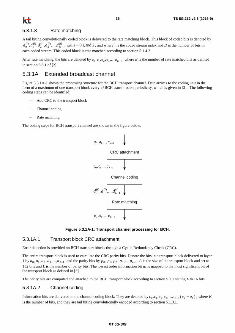
Figure 531-1 shows the processing structure for the BCH transport channel Data arrives to the coding unit in the form
of a maximum of one transport block every transmission time interval (TTI) of 40ms The following coding steps can
be identified
Add CRC to the transport block
Channel coding
Rate matching
The coding steps for BCH transport channel are shown in the figure below
KT 5G-SIG
TS 5G212 v23 (2016-9) 34
CRC attachment
Channel coding
Rate matching
110 Aaaa
110 Kccc
110 Eeee
)(1
)(1
)(0
iD
iiddd
Figure 531-1 Transport channel processing for BCH
5311 Transport block CRC attachment
Error detection is provided on BCH transport blocks through a Cyclic Redundancy Check (CRC)
The entire transport block is used to calculate the CRC parity bits Denote the bits in a transport block delivered to layer
1 by 13210 Aaaaaa and the parity bits by 13210 Lppppp A is the size of the transport block and set to
16 bits and L is the number of parity bits The lowest order information bit a0 is mapped to the most significant bit of
the transport block as defined in [5]
The parity bits are computed and attached to the BCH transport block according to section 511 setting L to 16 bits
After the attachment the CRC bits are scrambled according to the 5G Node transmit antenna configuration with the
sequence 1510 antantant xxx as indicated in Table 5311-1 to form the sequence of bits 13210 Kccccc where
kk ac for k = 0 1 2 hellip A-1
2mod AkantAkk xpc for k = A A+1 A+2 A+15
Table 5311-1 CRC mask for xPBCH
Number of transmit antenna ports for BRS PBCH CRC mask
1510 antantant xxx
1 lt0 0 0 0 0 0 0 0 0 0 0 0 0 0 0 0gt
2 lt1 1 1 1 1 1 1 1 1 1 1 1 1 1 1 1gt
4 lt0 1 0 1 0 1 0 1 0 1 0 1 0 1 0 1gt
8 lt1 0 1 0 1 0 1 0 1 0 1 0 1 0 1 0gt
5312 Channel coding
Information bits are delivered to the channel coding block They are denoted by 13210 Kccccc where K is the
number of bits and they are tail biting convolutionally encoded according to section 5131
After encoding the bits are denoted by)(1
)(3
)(2
)(1
)(0
iD
iiiiddddd with 2 and 10i and where D is the number of bits
on the i-th coded stream ie KD
KT 5G-SIG
TS 5G212 v23 (2016-9) 35
5313 Rate matching
A tail biting convolutionally coded block is delivered to the rate matching block This block of coded bits is denoted by)(1
)(3
)(2
)(1
)(0
iD
iiiiddddd with 2 and 10i and where i is the coded stream index and D is the number of bits in
each coded stream This coded block is rate matched according to section 5142
After rate matching the bits are denoted by 13210 Eeeeee where E is the number of rate matched bits as defined
in section 661 of [2]
531A Extended broadcast channel
Figure 531A-1 shows the processing structure for the BCH transport channel Data arrives to the coding unit in the
form of a maximum of one transport block every ePBCH transmission periodicity which is given in [2] The following
coding steps can be identified
Add CRC to the transport block
Channel coding
Rate matching
The coding steps for BCH transport channel are shown in the figure below
CRC attachment
Channel coding
Rate matching
110 Aaaa
110 Kccc
110 Eeee
)(1
)(1
)(0
iD
iiddd
Figure 531A-1 Transport channel processing for BCH
531A1 Transport block CRC attachment
Error detection is provided on BCH transport blocks through a Cyclic Redundancy Check (CRC)
The entire transport block is used to calculate the CRC parity bits Denote the bits in a transport block delivered to layer
1 by 13210 Aaaaaa and the parity bits by 13210 Lppppp A is the size of the transport block and set to
152 bits and L is the number of parity bits The lowest order information bit a0 is mapped to the most significant bit of
the transport block as defined in [5]
The parity bits are computed and attached to the BCH transport block according to section 511 setting L to 16 bits
531A2 Channel coding
Information bits are delivered to the channel coding block They are denoted by 13210 Kccccc ( kk ac ) where K
is the number of bits and they are tail biting convolutionally encoded according to section 5131
KT 5G-SIG
TS 5G212 v23 (2016-9) 36
After encoding the bits are denoted by)(1
)(3
)(2
)(1
)(0
iD
iiiiddddd with 2 and 10i and where D is the number of bits
on the i-th coded stream ie KD
531A3 Rate matching
A tail biting convolutionally coded block is delivered to the rate matching block This block of coded bits is denoted by)(1
)(3
)(2
)(1
)(0
iD
iiiiddddd with 2 and 10i and where i is the coded stream index and D is the number of bits in
each coded stream This coded block is rate matched according to section 5142
After rate matching the bits are denoted by 13210 Eeeeee where E is the number of rate matched bits as defined
in section 661 of [2]
532 Downlink shared channel
The processing structure for each transport block for the DL-SCH transport channel
Figure 532-1 shows the processing structure for each transport block for the DL-SCH transport channel Data arrives
to the coding unit in the form of a maximum of two transport blocks every transmission time interval (TTI) per DL cell
The following coding steps can be identified for each transport block of a DL cell
Add CRC to the transport block
Code block segmentation
Channel coding
Rate matching
Code block concatenation
The coding steps for one transport block of DL-SCH are shown in the figure below The same processing applies for
each transport block on each DL cell
KT 5G-SIG
TS 5G212 v23 (2016-9) 37
Channel coding
Rate matching
Code block
concatenation
110 Aaaa
110 Bbbb
110 rKrrr ccc
110 rDrrr ddd
110 rErrr eee
110 Gfff
Transport block
CRC attachment
Code block segmentation
Figure 532-1 Transport block processing for DL-SCH
5321 Transport block CRC attachment
Error detection is provided on transport blocks through a Cyclic Redundancy Check (CRC)
The entire transport block is used to calculate the CRC parity bits Denote the bits in a transport block delivered to layer
1 by 13210 Aaaaaa and the parity bits by 13210 Lppppp A is the size of the transport block and L is the
number of parity bits The lowest order information bit a0 is mapped to the most significant bit of the transport block as
defined in section 611 of [4]
The parity bits are computed and attached to the transport block according to section 511 setting L to 24 bits and using
the generator polynomial gCRC24A(D)
5322 Code block segmentation
The bits input to the code block segmentation are denoted by 13210 Bbbbbb where B is the number of bits in the
transport block (including CRC)
The bits after code block segmentation are denoted by 13210 rKrrrrr ccccc where r is the code block number
and Kr is the number of bits for code block number r
5323 Channel coding
Code blocks are delivered to the channel coding block They are denoted by 13210 rKrrrrr ccccc where r is
the code block number and Kr is the number of bits in code block number r The total number of code blocks is denoted
by C and each code block is individually LDPC encoded according to section 5132
KT 5G-SIG
TS 5G212 v23 (2016-9) 38
After encoding the bits are denoted by dr0 dr1 dr2 hellip dr(Dr-1) with Dr = Nldpc is the number of bits on the i-th coded
stream for code block number r
5324 Rate matching
LDPC coded blocks are delivered to the rate matching block They are denoted by dr0 dr1 dr2 hellip dr(Dr-1) where r is the
code block number i is the coded stream index and Dr = Nldpc is the number of bits in each coded stream of code block
number r The total number of code blocks is denoted by C and each coded block is individually rate matched according
to section 5141
After rate matching the bits are denoted by 13210 rErrrrr eeeee where r is the coded block number and where rE
is the number of rate matched bits for code block number r
5325 Code block concatenation
The bits input to the code block concatenation block are denoted by 13210 rErrrrr eeeee for 10 Cr and
where rE is the number of rate matched bits for the r-th code block
Code block concatenation is performed according to section 515
The bits after code block concatenation are denoted by 13210 Gfffff where G is the total number of coded bits
for transmission This sequence of coded bits corresponding to one transport block after code block concatenation is
referred to as one codeword in section 631 of [2] In case of multiple transport blocks per TTI the transport block to
codeword mapping is specified according to section 53315 53315A or 53315B depending on the DCI Format
533 Downlink control information
Figure 533-1 shows the processing structure for one DCI The following coding steps can be identified
Information element multiplexing
CRC attachment
Channel coding
Rate matching
The coding steps for DCI are shown in the figure below
CRC attachment
Channel coding
Rate matching
110 Aaaa
110 Kccc
)(1
)(1
)(0
iD
iiddd
110 Eeee
Figure 533-1 Processing for one DCI
KT 5G-SIG
TS 5G212 v23 (2016-9) 39
5331 DCI formats
The fields defined in the DCI formats below are mapped to the information bits a0 to aA-1 as follows
Each field is mapped in the order in which it appears in the description including the zero-padding bit(s) if any with
the first field mapped to the lowest order information bit a0 and each successive field mapped to higher order
information bits The most significant bit of each field is mapped to the lowest order information bit for that field eg
the most significant bit of the first field is mapped to a0
Note All DCI formats shall have the same payload size of 60 bits
53311 Format A1
DCI format A1 is used for the scheduling of xPUSCH
The following information is transmitted by means of the DCI format A1 at the subframe index n
- DCI format discriminator ndash 2 bits where 00 indicates format A1
- xPUSCH range ndash 2bits as defined in Section 92 of [3]
- Transmission timing of xPUSCH ndash 3 bits where this field indicates transmission time offset value lisin0 1 hellip
7
If this DCI format assigns more than zero RB or requests SRS then the corresponding xPUSCH is
scheduled in subframe index n+4+l+m
Otherwise this field shall be set to all zeros
where the value of m is indicated by the ldquotransmission timing of CSI-RS BRRSrdquo field
- RB assignment ndash 9 bits
If the indicated value is smaller than or equal to 324 then this field assigns more than zero RB as
described in Section 92 of [3]
Else if the indicated value is equal to 325 then this format does not assign any of RB
Else if the indicated value is equal to 326 then this format does not assign any of RB and used for
random access procedure initiated by a xPDCCH order
Otherwise then this format is assumed to be misconfigured and UE shall discard the corresponding
xPDCCH
If this DCI format assigns more than zero RB
- HARQ process number ndash 4 bits
- MCS ndash 4 bits
- NDI ndash 1 bit
Else if this DCI format is used for random access procedure initiated by a xPDCCH order
- Frequency band index ndash 3 bits as defined in 57 of [2]
- OCC indicator ndash 1 bit as defined in 57 of [2]
- Cyclic shift indicator ndash 2 bits as defined in 57 of [2]
- Reserved ndash 3 bits which shall be set to all zeros
KT 5G-SIG
TS 5G212 v23 (2016-9) 40
Otherwise
- Reserved ndash 9 bits which shall be set to all zeros
- CSI BSI BRI request ndash 3 bits
If the indicated value is 000 then none of CSIBSIBRI is requested
Else if the indicated value is 001 then this DCI format triggers BSI reporting
Else if the indicated value is 010 then this DCI format allocates BRRS and also triggers corresponding
BRI reporting
Else if the indicated value is 011 then this DCI format allocates BRRS but does not trigger BRI
reporting
Else if the indicated value is 100 then this DCI format allocates CSI-RS and also triggers corresponding
CSI reporting
The values 101 110 and 111 are reserved
- Transmission timing of CSI-RS BRRS ndash 2 bits where this field indicates transmission time offset value misin0 1 2 3
If this DCI format allocates either of CSI-RS or BRRS then the corresponding transmission is allocated
in subframe n + m
Otherwise it shall be set to all zeros
- Indication of OFDM symbol index for CSI-RS BRRS allocations ndash 2 bits
If this DCI format allocates CSI-RS then this field indicates OFDM symbols used for CSI-RS
transmission
00 13th 01 14th 10 13amp14th 11 Reserved
Else if this DCI format allocates BRRS and higher-layer gives either of 1 or 2 symbol BRRS
configuration then this field indicates OFDM symbols used for BRRS transmission
00 13th 01 14th 10 13amp14th 11 Reserved
Else if this DCI format allocates BRRS and higher-layer gives either of 5 or 10 symbol BRRS
configuration then this field indicates OFDM symbols used for BRRS transmission
00 5 symbols in slot 0 01 5 symbols in slot 1 10 10 symbols 11 Reserved
Otherwise it shall be set to all zeros
If this DCI format allocates either of CSI-RS or BRRS transmission
- Process indicator ndash 2 bits
00 Process 0 01 Process 1 10 Process 2 11 Process 3
Else if this DCI format triggers BSI request
- Number of BSI reports ndash 2 bits
00 1 BSI report 01 2 BSI reports 10 4 BSI reports 11 Reserved
Otherwise
- Reserved ndash 2 bits which shall be set to all zeros
KT 5G-SIG
TS 5G212 v23 (2016-9) 41
- UCI on xPUSCH wo xUL-SCH data indicator ndash 1 bit
If no UCI report is triggered then this field is invalid and shall be set to zero
Otherwise the indicated value of 0 allows multiplexing of xUL-SCH data and UCI and the indicated
value of 1 allows only UCI transmission on xPUSCH
- Beam switch indication ndash 1 bit as described in Section 511 and Section 521 of [3]
- SRS request ndash 3 bits
MSB 2 bits are used for the indication of SRS configurations
00 No SRS request 01 Config 0 10 Config 1 11 Config 2
LSB 1 bit
If SRS is not requested this field is invalid and shall be set to zero
If SRS is requested 0 indicates SRS transmission on the 13th
OFDM symbol and 1 indicates SRS
transmission on the 14th
OFDM symbol in subframe n + 4 + l + m+1
- DMRS RI and SCID indication ndash 4 bits as specified in Table 53311-1
- Precoding matrix indicator ndash 3 bits as specified in Table 533A2-1 of [2]
- TPC command for xPUSCH ndash 2 bits as defined in Section 6111 of [3]
- UL PCRS ndash 2 bits
00 No PCRS 01 PCRS on AP 50 10 PCRS on AP 51 11 PCRS on AP 50 and 51
Note If no PCRS is transmitted both PCRS Res are used for xPUSCH If PCRS is transmitted both PCRS
Res are not used for xPUSCH
If the number of information bits in format A1 is less than 60 bits zeros shall be appended to format A1 until the
payload size equals to 60 bits
Table 53311-1 Antenna port(s) scrambling identity and number of layers indication by UL DCI formats
Value Message
0 1 Layer port 40 nSCID = 0
1 1 Layer port 40 nSCID = 1
2 1 Layer port 41 nSCID = 0
3 1 Layer port 41 nSCID = 1
4 1 Layer port 42 nSCID = 0
5 1 Layer port 42 nSCID = 1
6 1 Layer port 43 nSCID = 0
7 1 Layer port 43 nSCID = 1
KT 5G-SIG
TS 5G212 v23 (2016-9) 42
8 2 Layers ports 40 41 nSCID = 0
9 2 Layers ports 40 41 nSCID = 1
10 2 Layers ports 42 43 nSCID = 0
11 2 Layers ports 42 43 nSCID = 1
12 - 15 Reserved
53312 Format A2
DCI format A2 is used for the scheduling of xPUSCH
All of the information fields in the DCI format A1 are also used for DCI format A2 except the following field
- DCI format discriminator ndash 2 bits where 01 indicates format A2
If the number of information bits in format A2 is less than 60 bits zeros shall be appended to format A2 until the
payload size equals to 60 bits
53313 Format B1
DCI format B1 is used for the scheduling of xPDSCH
The following information is transmitted by means of the DCI format B1 at the subframe index n
- DCI format discriminator ndash 2 bits where 10 indicates format B1
- xPDSCH range ndash 2bits as defined in Section 814 of [3]
- RB assignment ndash 9 bits
If the indicated value is smaller than or equal to 324 then this field assigns more than zero RB as
described in Section 814 of [3]
Else if the indicated value is equal to 325 then this format does not assign any of RB
Else if the indicated value is equal to 326 then this format does not assign any of RB and used for
random access procedure initiated by a xPDCCH order
Otherwise then this format is assumed to be misconfigured and UE shall discard the corresponding
xPDCCH
If this DCI format assigns more than zero RB
- HARQ process number ndash 4 bits
- MCS ndash 4 bits
- NDI ndash 1 bit
- Redundancy version ndash 2 bits
- Bit-mapping index for HARQ-ACK multiplexing (BMI) ndash 3bits as described in Section 85 of [3]
Else if this DCI format is used for random access procedure initiated by a xPDCCH order
- Frequency band index ndash 3 bits
KT 5G-SIG
TS 5G212 v23 (2016-9) 43
- OCC indicator ndash 1 bit
- Cyclic shift indicator ndash 2 bits
- Reserved ndash 8 bits which shall be set to all zeros
Otherwise
- Reserved ndash 14 bits which shall be set to all zeros
- CSI BSI BRI request ndash 3 bits
If the indicated value is 000 then none of CSIBSIBRI is requested
Else if the indicated value is 001 then this DCI format triggers BSI reporting
Else if the indicated value is 010 then this DCI format allocates BRRS and also triggers corresponding
BRI reporting
Else if the indicated value is 011 then this DCI format allocates BRRS but does not trigger BRI
reporting
Else if the indicated value is 100 then this DCI format allocates CSI-RS and also triggers corresponding
CSI reporting
The indicated values 101 110 and 111 are reserved
- Transmission timing of CSI-RS BRRS ndash 2 bits where this field indicates transmission time offset value misin0 1 2 3
If this DCI format allocates either of CSI-RS or BRRS then the corresponding transmission is allocated
in subframe n + m
Otherwise it shall be set to all zeros
- Indication of OFDM symbol index for CSI-RS BRRS allocations ndash 2 bits
If this DCI format allocates CSI-RS then this field indicates OFDM symbols used for CSI-RS
transmission
00 13th 01 14th 10 13amp14th 11 Reserved
Else if this DCI format allocates BRRS and higher-layer gives either of 1 or 2 symbol BRRS
configuration then this field indicates OFDM symbols used for BRRS transmission
00 13th 01 14th 10 13amp14th 11 Reserved
Else if this DCI format allocates BRRS and higher-layer gives either of 5 or 10 symbol BRRS
configuration then this field indicates OFDM symbols used for BRRS transmission
00 5 symbols in slot 0 01 5 symbols in slot 1 10 10 symbols 11 Reserved
Otherwise it shall be set to all zeros
If this DCI format allocates either of CSI-RS or BRRS transmission
- Process indicator ndash 2 bits
00 Process 0 01 Process 1 10 Process 2 11 Process 3
Otherwise
- Reserved ndash 2 bits which shall be set to all zeros
KT 5G-SIG
TS 5G212 v23 (2016-9) 44
- Transmission timing of xPUCCH for UCI report ndash 3 bits where this field indicates transmission time offset
value kisin0 1 2 hellip 7
xPUCCH transmission is allocated in subframe index n + 4 + k + m
- Frequency resource index of xPUCCH for UCI report ndash 4 bits
- Beam switch indication ndash 1 bit as described in Section 511 and Section 521 of [3]
- SRS request ndash 3 bits
MSB 2 bits are used for the indication of SRS configurations
00 No SRS request 01 Config 0 10 Config 1 11 Config 2
LSB 1 bit
If SRS is not requested this field is invalid and shall be set to zero
If SRS is requested 0 indicates SRS transmission on the 13th
OFDM symbol and 1 indicates SRS
transmission on the 14th
OFDM symbol in subframe n + 4 + m + k + 1
- Antenna port(s) and number of layers indicationndash4 bits as specified in Table 53313-1
- Scrambling identity ndash 1bit
If the indicated value is 0 then nSCID = 0
If the indicated value is 1 then nSCID = 1
- TPC command for xPUCCH ndash 2 bits as defined in Section 612 of [3]
- DL PCRS ndash 2 bits
00 No PCRS 01 PCRS on AP 60 10 PCRS on AP 61 11 PCRS on AP 60 and 61
If the number of information bits in format B1 is less than 60 bits zeros shall be appended to format B1 until the
payload size equals to 60 bits
Table 53313-1 Antenna port(s) and number of layers indication by DL DCI formats
Value Message
0 1 Layer port 8 (Ch estimation wo OCC)
1 1 Layer port 9 (Ch estimation wo OCC)
2 1 Layer port 10 (Ch estimation wo OCC)
3 1 Layer port 11 (Ch estimation wo OCC)
4 2 Layers ports 8 9 (Ch estimation wo OCC)
5 2 Layers ports 10 11 (Ch estimation wo OCC)
6 2 Layers ports 8 12 (OCC=2)
7 2 Layers ports 9 13 (OCC=2)
8 2 Layers ports 10 14 (OCC=2)
9 2 Layers ports 11 15 (OCC=2)
10-15 Reserved
KT 5G-SIG
TS 5G212 v23 (2016-9) 45
53314 Format B2
DCI format B2 is used for the scheduling of xPDSCH
All of the information fields in the DCI format B1 are also used for DCI format B2 except the following field
- DCI format discriminator ndash 2 bits where 11 indicates format B2
If the number of information bits in format B2 is less than 60 bits zeros shall be appended to format B2 until the
payload size equals to 60 bits
5332 CRC attachment
Error detection is provided on DCI transmissions through a Cyclic Redundancy Check (CRC)
The entire payload is used to calculate the CRC parity bits Denote the bits of the payload by 13210 Aaaaaa and
the parity bits by 13210 Lppppp A is the payload size and L is the number of parity bits
The parity bits are computed and attached according to section 511 setting L to 16 bits resulting in
13210 Bbbbbb where B = A+ L
After attachment the CRC parity bits are scrambled with the corresponding RNTI 1510 rntirntirnti xxx where 0rntix
corresponds to the MSB of the RNTI to form the sequence of bits 13210 Bccccc The relation between ck and bk
is
kk bc for k = 0 1 2 hellip A-1
2mod Akrntikk xbc for k = A A+1 A+2 A+15
5333 Channel coding
Information bits are delivered to the channel coding block They are denoted by 13210 Kccccc where K is the
number of bits and they are tail biting convolutionally encoded according to section 5131
After encoding the bits are denoted by )(1
)(3
)(2
)(1
)(0
iD
iiiiddddd with 2 and 10i and where D is the number of
bits on the i-th coded stream ie KD
5334 Rate matching
A tail biting convolutionally coded block is delivered to the rate matching block This block of coded bits is denoted by
)(1
)(3
)(2
)(1
)(0
iD
iiiiddddd with 2 and 10i and where i is the coded stream index and D is the number of bits in
each coded stream This coded block is rate matched according to section 5142
After rate matching the bits are denoted by 13210 Eeeeee where E is the number of rate matched bits
Page 2
KT 5G-SIG
TS 5G212 v23 (2016-9) 2
Document History
Version Date Change
10 2016-02-17 First Draft Version
21 2016-07-13 Pre-final Version
22 2016-08-29 Apply CR for clarification
23 2016-09-19 Changes for technicaleditorial correction (including DCI format B1
update)
KT 5G-SIG
TS 5G212 v23 (2016-9) 3
Contents
Foreword 5
1 Scope 6
2 References 6
3 Definitions symbols and abbreviations 6
31 Definitions 6
32 Symbols 6
33 Abbreviations 6
4 Mapping to physical channels 7
41 Uplink 7
42 Downlink 7
5 Channel coding multiplexing and interleaving 7
51 Generic procedures 7
511 CRC calculation 7
512 Code block segmentation 8
513 Channel coding 10
5131 Tail biting convolutional coding 10
5132 LDPC encoder 11
514 Rate matching 16
5141 Rate matching for LDPC coded transport channels 16
5142 Rate matching for convolutionally coded transport channels and control information 17
515 Code block concatenation 19
52 Uplink transport channels and control information 20
521 Random access channel 20
522 Uplink shared channel 20
5221 Transport block CRC attachment 21
5222 Code block segmentation 21
5223 Channel coding of UL-SCH 22
5224 Rate matching 22
5225 Code block concatenation 22
5226 Channel coding of control information 22
5227 Data and control multiplexing 27
5228 Channel interleaver 27
523 Uplink control information on xPUCCH 28
5231 Channel coding for UCI HARQ-ACK 29
5232 Channel coding for UCI scheduling request 30
5233 Channel coding for UCI channel quality information 30
5234 Channel coding for UCI Beam related information feedback 31
5235 Channel coding for multiple UCIs 32
524 Uplink control information on xPUSCH without UL-SCH data 32
5241 Channel coding of control information 32
5242 Control information mapping 33
5243 Channel interleaver 33
53 Downlink transport channels and control information 33
531 Broadcast channel 33
5311 Transport block CRC attachment 34
5312 Channel coding 34
5313 Rate matching 35
531A Extended broadcast channel 35
531A1 Transport block CRC attachment 35
531A2 Channel coding 35
531A3 Rate matching 36
532 Downlink shared channel 36
5321 Transport block CRC attachment 37
5322 Code block segmentation 37
5323 Channel coding 37
KT 5G-SIG
TS 5G212 v23 (2016-9) 4
5324 Rate matching 38
5325 Code block concatenation 38
533 Downlink control information 38
5331 DCI formats 39
53311 Format A1 39
53312 Format A2 42
53313 Format B1 42
53314 Format B2 45
5332 CRC attachment 45
5333 Channel coding 45 5334 Rate matching 45
KT 5G-SIG
TS 5G212 v23 (2016-9) 5
Foreword
This Technical Specification has been produced by the KT PyeongChang 5G Special Interest Group (KT 5G-SIG)
KT 5G-SIG
TS 5G212 v23 (2016-9) 6
1 Scope
The present document specifies the coding multiplexing and mapping to physical channels for 5G Radio Access (5G
RA)
2 References
The following documents contain provisions which through reference in this text constitute provisions of the present
document
References are either specific (identified by date of publication edition number version number etc) or
non-specific
For a specific reference subsequent revisions do not apply
[1] TS 5G201 5G Radio Access (5G RA) Physical layer General description
[2] TS 5G211 5G Radio Access (5G RA) Physical channel and modulation
[3] TS 5G213 5G Radio Access (5G RA) Physical layer procedures
[4] TS 5G321 ldquo5G Radio Access (5G RA) 5G Medium Access Control Protocolrdquo
[5] TS 5G331 ldquo5G Radio Access (5G RA) 5G Radio Resource Control (5G-RRC) Protocol
Specificationrdquo
3 Definitions symbols and abbreviations
31 Definitions
32 Symbols
For the purposes of the present document the following symbols apply
33 Abbreviations
For the purposes of the present document the following abbreviations apply
BCH Broadcast channel
BQI Beam Quality Information
BRS Beam measurement Reference Signal
CP Cyclic Prefix
CSI Channel State Information
DCI Downlink Control Information
DL-SCH Downlink Shared channel
FDD Frequency Division Duplexing
LDPC Low Density Parity Check
xPBCH Physical Broadcast channel
xPDCCH Physical Downlink Control channel
xPDSCH Physical Downlink Shared channel
PMI Precoding Matrix Indicator
xPRACH Physical Random Access channel
xPUSCH Physical Uplink Shared channel
xRACH Random Access channel
RI Rank Indication
SR Scheduling Request
SRS Sounding Reference Signal
TDD Time Division Duplexing
TPMI Transmitted Precoding Matrix Indicator
KT 5G-SIG
TS 5G212 v23 (2016-9) 7
UCI Uplink Control Information
UL-SCH Uplink Shared channel
4 Mapping to physical channels
41 Uplink
Table 41-1 specifies the mapping of the uplink transport channels to their corresponding physical channels Table 41-2
specifies the mapping of the uplink control channel information to its corresponding physical channel
Table 41-1
TrCH Physical Channel
UL-SCH xPUSCH
RACH xPRACH
Table 41-2
Control information Physical Channel
UCI xPUCCH xPUSCH
42 Downlink
Table 42-1 specifies the mapping of the downlink transport channels to their corresponding physical channels Table
42-2 specifies the mapping of the downlink control channel information to its corresponding physical channel
Table 42-1
TrCH Physical Channel
DL-SCH xPDSCH
BCH xPBCH ePBCH
Table 42-2
Control information Physical Channel
DCI xPDCCH
5 Channel coding multiplexing and interleaving
Data and control streams fromto MAC layer are encoded decoded to offer transport and control services over the radio
transmission link Channel coding scheme is a combination of error detection error correcting rate matching
interleaving and transport channel or control information mapping ontosplitting from physical channels
51 Generic procedures
This section contains coding procedures which are used for more than one transport channel or control information type
511 CRC calculation
Denote the input bits to the CRC computation by 13210 Aaaaaa and the parity bits by 13210 Lppppp A
is the size of the input sequence and L is the number of parity bits The parity bits are generated by one of the following
cyclic generator polynomials
- gCRC24A(D) = [D24
+ D23
+ D18
+ D17
+ D14
+ D11
+ D10
+ D7 + D
6 + D
5 + D
4 + D
3 + D + 1] and
- gCRC16(D) = [D16
+ D12
+ D5 + 1] for a CRC length L = 16
KT 5G-SIG
TS 5G212 v23 (2016-9) 8
- gCRC8(D) = [D8 + D
7 + D
4 + D
3 + D + 1] for a CRC length of L = 8
The encoding is performed in a systematic form which means that in GF(2) the polynomial
231
2222
123
024
122
123
0 pDpDpDpDaDaDa AAA
yields a remainder equal to 0 when divided by the corresponding length-24 CRC generator polynomial gCRC24A(D) the
polynomial
151
1414
115
016
114
115
0 pDpDpDpDaDaDa AAA
yields a remainder equal to 0 when divided by gCRC16(D) and the polynomial
7
1
6
6
1
7
0
8
1
6
1
7
0 pDpDpDpDaDaDa A
AA
yields a remainder equal to 0 when divided by gCRC8(D)
The bits after CRC attachment are denoted by 13210 Bbbbbb where B = A+ L The relation between ak and bk is
kk ab for k = 0 1 2 hellip A-1
Akk pb for k = A A+1 A+2 A+L-1
512 Code block segmentation
The input bit sequence to the code block segmentation is denoted by 13210 Bbbbbb where B gt 0 If B is larger
than the maximum code block size Kmax segmentation of the input bit sequence is performed
The maximum and minimum code block sizes depending on the code rate and Coding Type are depicted in Table 512-
1
Table 512-1 Kmax and Kmin
Coding Type Code Rate Kmax Kmin
Type 1 56 1620 540
34 1458 486
23 1296 432
12 972 324
Type 2 13 1620 540
If the number of filler bits Fr calculated below is not 0 filler bits are added to r-th blocks where r is the code block
number
Note that if B lt Kmin filler bits are added to the end of the code block
The filler bits shall be set to ltNULLgt at the input to the encoder
For a given code rate total number of code blocks C is determined by
if Ble Kmax
Number of code blocks 1C
else
Number of code blocks maxΒΚC
end if
KT 5G-SIG
TS 5G212 v23 (2016-9) 9
The bits output from code block segmentation for C 0 are denoted by 13210 rKrrrrr ccccc where r
is the code block number and Kr is the number of bits for the code block number r
Number of bits in each code block (applicable for C 0 only)
if C = 1
1198700 = lceil119861119870119898119894119899rceil ∙ 119870119898119894119899
1198650 = 1198700 minus 119861
else
119869 = lceil119861119862rceil
119870 prime = lceil119869119870119898119894119899rceil ∙ 119870119898119894119899
119865prime = 119870 prime ∙ 119862 minus 119861
120574 = 119865primemod 119862
for r = 0 to 119862 minus 1
if 119903 le 119862 minus 120574 minus 1
119865119903 = lfloor119865prime119862rfloor
119870119903 = lceil119861119862rceil + 119865119903
else
119865119903 = lceil119865prime119862rceil
119870119903 = lfloor119861119862rfloor + 119865119903
end if
end for r
end if
s = 0
for r = 0 to 119862 minus 1
for k = 0 to Kr ndash Fr ndash 1
srk bc
1 ss
end for k
The filler bits ltNULLgt shall be inserted end of the each code block
for k = Kr ndash Fr ndash 1 to Kr -1
crk = ltNULLgt
end for k
end for r
KT 5G-SIG
TS 5G212 v23 (2016-9) 10
513 Channel coding
The bit sequence input for a given code block to channel coding is denoted by 13210 Kccccc where K is the
number of bits to encode After encoding the bits are denoted by)(1
)(3
)(2
)(1
)(0
iD
iiiiddddd and
1D3210 ddddd for
convolutional coding scheme and LDPC coding scheme respectively where D is the number of encoded bits per output
stream and i indexes the encoder output stream The relation between kc and )(ikd and between K and D is dependent
on the channel coding scheme
The following channel coding schemes can be applied to TrCHs
- Tail biting convolutional coding
- LDPC coding
Usage of coding scheme and coding rate for the different types of TrCH is shown in Table 513-1 Usage of coding
scheme and coding rate for the different control information types is shown in Table 513-2
The values of D in connection with each coding scheme
- tail biting convolutional coding with rate 13 D = K
- LDPC coding with code rate R D = KR
The range for the output stream index i is 0 1 and 2 for tail biting convolutional coding scheme
Table 513-1 Usage of channel coding scheme and coding rate for TrCHs
TrCH Coding scheme Coding rate
UL-SCH LDPC coding variable
DL-SCH
BCH Tail biting
convolutional coding
13
Table 513-2 Usage of channel coding scheme and coding rate for control information
Control Information Coding scheme Coding rate
DCI Tail biting
convolutional coding
13
UCI
Block code variable
Tail biting convolutional
coding 13
5131 Tail biting convolutional coding
A tail biting convolutional code with constraint length 7 and coding rate 13 is defined
The configuration of the convolutional encoder is presented in Figure 5131-1
The initial value of the shift register of the encoder shall be set to the values corresponding to the last 6 information bits
in the input stream so that the initial and final states of the shift register are the same Therefore denoting the shift
register of the encoder by 5210 ssss then the initial value of the shift register shall be set to
iKi cs 1
KT 5G-SIG
TS 5G212 v23 (2016-9) 11
D D D DD D
G0 = 133 (octal)
G1 = 171 (octal)
G2 = 165 (octal)
kc
)0(kd
)1(kd
)2(kd
Figure 5131-1 Rate 13 tail biting convolutional encoder
The encoder output streams)0(
kd )1(
kd and )2(
kd correspond to the first second and third parity streams respectively
as shown in Figure 5131-1
5132 LDPC encoder
The K bits including filler bits (c0 c1 c2 hellip cK-1) are encoded based on D-K by D parity check matrix (H) where D is
number of encoded bits and D - K is the number of parity check bits The parity check bits (p0 p1 p2 hellip pD-K -1) are
obtained so that H∙ dT = 0 where d =(c0c1c2 hellip cK-1 p0 p1 p2 hellip pD-K-1) is coded bits stream
The parity check matrix H is defined as
119867 =
[
11987511988600 11987511988601 11987511988602
11987511988610 11987511988611 11987511988612
11987511988620 11987511988621 11987511988622
⋯119875
1198860119873119897119889119901119888_119887minus2 1198751198860119873119897119889119901119888_119887minus1
1198751198861119873119897119889119901119888_119887minus2 119875
1198861119873119897119889119901119888_119887minus1
1198751198862119873119897119889119901119888_119887minus2 119875
1198862119873119897119889119901119888_119887minus1
⋮ ⋱ ⋮
119875119886119873119901119886119903119894119905119910_119887minus10 119875
119886119873119901119886119903119894119905119910_119887minus11 119875119886119873119901119886119903119894119905119910_119887minus12 ⋯ 119875
119886119873119901119886119903119894119905119910_119887minus1119873119897119889119901119888_119887minus2 119875119886119873119901119886119903119894119905119910_119887minus1119873119897119889119901119888_119887minus1]
where Paij (0leiltNparity_b 0lejltNldpc_b) is cyclic-permutation matrix obtained from the zero matrix and the Z by Z identity
matrix by cyclically shifted the columns to the right by aij elements The value of Z is shift size obtained by Z =lceil119870119870119898119894119899rceil ∙ 27 where Kmin is given in Table 512-1
The matrix Paij is Z by Z zero matrix when aij is -1 The codeword length D information length K and number of parity
bits D-K is equal to Nldpc_b x Z Kldpc_b x Z and Npairty_b x Z respectively The parameters Nldpc_b Kldpc_b and Nparity_b
according to code rates are depicted in Table 5132-1
Table 5132-1 Parameters of parity check matrix
Coding Type Code Rate Nldpc_b Kldpc_b Nparity_b
Type 1
56 24 20 4
34 24 18 6
23 24 16 8
12 24 12 12
Type 2 13 60 20 40
For Type 1 the parity check matrix is obtained based on Tables 5132-2 5132-3 5132-4 and 5132-5 which
show the exponents (aij) of parity check matrix when the code rate equals 56 34 23 and 12 for each encoded bits
respectively
For Type 2 the parity check matrix is obtained based on Table 5132-6 which shows the exponents (aij) of parity check
matrix when the Z equals 81 The set of exponents (aij) are used to determine the exponents for all other code length of
the same code rate Z=27 or 54 The exponents aij(Z) for code size corresponding to shift size Z determined above are
derived from aij by using a modulo function as below
0mod
0
ijij
ijij
ij aifZa
aifaZa
KT 5G-SIG
TS 5G212 v23 (2016-9) 12
Table 5132-2 Matrix exponents for Code rate R=56 Type 1
(a) D = 648 bits Z=27 bits
17 13 8 21 9 3 18 12 10 0 4 15 19 2 5 10 26 19 13 13 1 0 -1 -1
3 12 11 14 11 25 5 18 0 9 2 26 26 10 24 7 14 20 4 2 -1 0 0 -1
22 16 4 3 10 21 12 5 21 14 19 5 -1 8 5 18 11 5 5 15 0 -1 0 0
7 7 14 14 4 16 16 24 24 10 1 7 15 6 10 26 8 18 21 14 1 -1 -1 0
(b) D = 1296 bits Z=54 bits
48 29 37 52 2 16 6 14 53 31 34 5 18 42 53 31 45 -1 46 52 1 0 -1 -1
17 4 30 7 43 11 24 6 14 21 6 39 17 40 47 7 15 41 19 -1 -1 0 0 -1
7 2 51 31 46 23 16 11 53 40 10 7 46 53 33 35 -1 25 35 38 0 -1 0 0
19 48 41 1 10 7 36 47 5 29 52 52 31 10 26 6 3 2 -1 51 1 -1 -1 0
(c) D = 1944 bits Z=81 bits
13 48 80 66 4 74 7 30 76 52 37 60 -1 49 73 31 74 73 23 -1 1 0 -1 -1
69 63 74 56 64 77 57 65 6 16 51 -1 64 -1 68 9 48 62 54 27 -1 0 0 -1
51 15 0 80 24 25 42 54 44 71 71 9 67 35 -1 58 -1 29 -1 53 0 -1 0 0
16 29 36 41 44 56 59 37 50 24 -1 65 4 65 52 -1 4 -1 73 52 1 -1 -1 0
Table 5132-3 Matrix exponents for R=34 Type 1
(a) D = 648 bits Z=27 bits
16 17 22 24 9 3 14 -1 4 2 7 -1 26 -1 2 -1 21 -1 1 0 -1 -1 -1 -1
25 12 12 3 3 26 6 21 -1 15 22 -1 15 -1 4 -1 -1 16 -1 0 0 -1 -1 -1
25 18 26 16 22 23 9 -1 0 -1 4 -1 4 -1 8 23 11 -1 -1 -1 0 0 -1 -1
9 7 0 1 17 -1 -1 7 3 -1 3 23 -1 16 -1 -1 21 -1 0 -1 -1 0 0 -1
24 5 26 7 1 -1 -1 15 24 15 -1 8 -1 13 -1 13 -1 11 -1 -1 -1 -1 0 0
2 2 19 14 24 1 15 19 -1 21 -1 2 -1 24 -1 3 -1 2 1 -1 -1 -1 -1 0
(b) D = 1296 bits Z=54 bits
39 40 51 41 3 29 8 36 -1 14 -1 6 -1 33 -1 11 -1 4 1 0 -1 -1 -1 -1
48 21 47 9 48 35 51 -1 38 -1 28 -1 34 -1 50 -1 50 -1 -1 0 0 -1 -1 -1
30 39 28 42 50 39 5 17 -1 6 -1 18 -1 20 -1 15 -1 40 -1 -1 0 0 -1 -1
29 0 1 43 36 30 47 -1 49 -1 47 -1 3 -1 35 -1 34 -1 0 -1 -1 0 0 -1
1 32 11 23 10 44 12 7 -1 48 -1 4 -1 9 -1 17 -1 16 -1 -1 -1 -1 0 0
13 7 15 47 23 16 47 -1 43 -1 29 -1 52 -1 2 -1 53 -1 1 -1 -1 -1 -1 0
KT 5G-SIG
TS 5G212 v23 (2016-9) 13
(c) D = 1944 bits Z=81 bits
48 29 28 39 9 61 -1 -1 -1 63 45 80 -1 -1 -1 37 32 22 1 0 -1 -1 -1 -1
4 49 42 48 11 30 -1 -1 -1 49 17 41 37 15 -1 54 -1 -1 -1 0 0 -1 -1 -1
35 76 78 51 37 35 21 -1 17 64 -1 -1 -1 59 7 -1 -1 32 -1 -1 0 0 -1 -1
9 65 44 9 54 56 73 34 42 -1 -1 -1 35 -1 -1 -1 46 39 0 -1 -1 0 0 -1
3 62 7 80 68 26 -1 80 55 -1 36 -1 26 -1 9 -1 72 -1 -1 -1 -1 -1 0 0
26 75 33 21 69 59 3 38 -1 -1 -1 35 -1 62 36 26 -1 -1 1 -1 -1 -1 -1 0
Table 5132-4 Matrix exponents for R=23 Type 1
(a) D = 648 bits Z=27 bits
25 26 14 -1 20 -1 2 -1 4 -1 -1 8 -1 16 -1 18 1 0 -1 -1 -1 -1 -1 -1
10 9 15 11 -1 0 -1 1 -1 -1 18 -1 8 -1 10 -1 -1 0 0 -1 -1 -1 -1 -1
16 2 20 26 21 -1 6 -1 1 26 -1 7 -1 -1 -1 -1 -1 -1 0 0 -1 -1 -1 -1
10 13 5 0 -1 3 -1 7 -1 -1 26 -1 -1 13 -1 16 -1 -1 -1 0 0 -1 -1 -1
23 14 24 -1 12 -1 19 -1 17 -1 -1 -1 20 -1 21 -1 0 -1 -1 -1 0 0 -1 -1
6 22 9 20 -1 25 -1 17 -1 8 -1 14 -1 18 -1 -1 -1 -1 -1 -1 -1 0 0 -1
14 23 21 11 20 -1 24 -1 18 -1 19 -1 -1 -1 -1 22 -1 -1 -1 -1 -1 -1 0 0
17 11 11 20 -1 21 -1 26 -1 3 -1 -1 18 -1 26 -1 1 -1 -1 -1 -1 -1 -1 0
(b) D = 1296 bits Z=54 bits
39 31 22 43 -1 40 4 -1 11 -1 -1 50 -1 -1 -1 6 1 0 -1 -1 -1 -1 -1 -1
25 52 41 2 6 -1 14 -1 34 -1 -1 -1 24 -1 37 -1 -1 0 0 -1 -1 -1 -1 -1
43 31 29 0 21 -1 28 -1 -1 2 -1 -1 7 -1 17 -1 -1 -1 0 0 -1 -1 -1 -1
20 33 48 -1 4 13 -1 26 -1 -1 22 -1 -1 46 42 -1 -1 -1 -1 0 0 -1 -1 -1
45 7 18 51 12 25 -1 -1 -1 50 -1 -1 5 -1 -1 -1 0 -1 -1 -1 0 0 -1 -1
35 40 32 16 5 -1 -1 18 -1 -1 43 51 -1 32 -1 -1 -1 -1 -1 -1 -1 0 0 -1
9 24 13 22 28 -1 -1 37 -1 -1 25 -1 -1 52 -1 13 -1 -1 -1 -1 -1 -1 0 0
32 22 4 21 16 -1 -1 -1 27 28 -1 38 -1 -1 -1 8 1 -1 -1 -1 -1 -1 -1 0
(c) D = 1944 bits Z=81 bits
61 75 4 63 56 -1 -1 -1 -1 -1 -1 8 -1 2 17 25 1 0 -1 -1 -1 -1 -1 -1
56 74 77 20 -1 -1 -1 64 24 4 67 -1 7 -1 -1 -1 -1 0 0 -1 -1 -1 -1 -1
28 21 68 10 7 14 65 -1 -1 -1 23 -1 -1 -1 75 -1 -1 -1 0 0 -1 -1 -1 -1
48 38 43 78 76 -1 -1 -1 -1 5 36 -1 15 72 -1 -1 -1 -1 -1 0 0 -1 -1 -1
40 2 53 25 -1 52 62 -1 20 -1 -1 44 -1 -1 -1 -1 0 -1 -1 -1 0 0 -1 -1
69 23 64 10 22 -1 21 -1 -1 -1 -1 -1 68 23 29 -1 -1 -1 -1 -1 -1 0 0 -1
12 0 68 20 55 61 -1 40 -1 -1 -1 52 -1 -1 -1 44 -1 -1 -1 -1 -1 -1 0 0
58 8 34 64 78 -1 -1 11 78 24 -1 -1 -1 -1 -1 58 1 -1 -1 -1 -1 -1 -1 0
KT 5G-SIG
TS 5G212 v23 (2016-9) 14
Table 5132-5 Matrix exponents for R=12 Type 1
(a) D = 648 bits Z=27 bits
0 -1 -1 -1 0 0 -1 -1 0 -1 -1 0 1 0 -1 -1 -1 -1 -1 -1 -1 -1 -1 -1
22 0 -1 -1 17 -1 0 0 12 -1 -1 -1 -1 0 0 -1 -1 -1 -1 -1 -1 -1 -1 -1
6 -1 0 -1 10 -1 -1 -1 24 -1 0 -1 -1 -1 0 0 -1 -1 -1 -1 -1 -1 -1 -1
2 -1 -1 0 20 -1 -1 -1 25 0 -1 -1 -1 -1 -1 0 0 -1 -1 -1 -1 -1 -1 -1
23 -1 -1 -1 3 -1 -1 -1 0 -1 9 11 -1 -1 -1 -1 0 0 -1 -1 -1 -1 -1 -1
24 -1 23 1 17 -1 3 -1 10 -1 -1 -1 -1 -1 -1 -1 -1 0 0 -1 -1 -1 -1 -1
25 -1 -1 -1 8 -1 -1 -1 7 18 -1 -1 0 -1 -1 -1 -1 -1 0 0 -1 -1 -1 -1
13 24 -1 -1 0 -1 8 -1 6 -1 -1 -1 -1 -1 -1 -1 -1 -1 -1 0 0 -1 -1 -1
7 20 -1 16 22 10 -1 -1 23 -1 -1 -1 -1 -1 -1 -1 -1 -1 -1 -1 0 0 -1 -1
11 -1 -1 -1 19 -1 -1 -1 13 -1 3 17 -1 -1 -1 -1 -1 -1 -1 -1 -1 0 0 -1
25 -1 8 -1 23 18 -1 14 9 -1 -1 -1 -1 -1 -1 -1 -1 -1 -1 -1 -1 -1 0 0
3 -1 -1 -1 16 -1 -1 2 25 5 -1 -1 1 -1 -1 -1 -1 -1 -1 -1 -1 -1 -1 0
(b) D = 1296 bits Z=54 bits
40 -1 -1 -1 22 -1 49 23 43 -1 -1 -1 1 0 -1 -1 -1 -1 -1 -1 -1 -1 -1 -1
50 1 -1 -1 48 35 -1 -1 13 -1 30 -1 -1 0 0 -1 -1 -1 -1 -1 -1 -1 -1 -1
39 50 -1 -1 4 -1 2 -1 -1 -1 -1 49 -1 -1 0 0 -1 -1 -1 -1 -1 -1 -1 -1
33 -1 -1 38 37 -1 -1 4 1 -1 -1 -1 -1 -1 -1 0 0 -1 -1 -1 -1 -1 -1 -1
45 -1 -1 -1 0 22 -1 -1 20 42 -1 -1 -1 -1 -1 -1 0 0 -1 -1 -1 -1 -1 -1
51 -1 -1 48 35 -1 -1 -1 44 -1 18 -1 -1 -1 -1 -1 -1 0 0 -1 -1 -1 -1 -1
47 11 -1 -1 -1 17 -1 -1 51 -1 -1 -1 0 -1 -1 -1 -1 -1 0 0 -1 -1 -1 -1
5 -1 25 -1 6 -1 45 -1 13 40 -1 -1 -1 -1 -1 -1 -1 -1 -1 0 0 -1 -1 -1
33 -1 -1 34 24 -1 -1 -1 23 -1 -1 46 -1 -1 -1 -1 -1 -1 -1 -1 0 0 -1 -1
1 -1 27 -1 1 -1 -1 -1 38 -1 44 -1 -1 -1 -1 -1 -1 -1 -1 -1 -1 0 0 -1
-1 18 -1 -1 23 -1 -1 8 0 35 -1 -1 -1 -1 -1 -1 -1 -1 -1 -1 -1 -1 0 0
49 -1 17 -1 30 -1 -1 -1 34 -1 -1 19 1 -1 -1 -1 -1 -1 -1 -1 -1 -1 -1 0
(c) D = 1944 bits Z=81 bits
57 -1 -1 -1 50 -1 11 -1 50 -1 79 -1 1 0 -1 -1 -1 -1 -1 -1 -1 -1 -1 -1
3 -1 28 -1 0 -1 -1 -1 55 7 -1 -1 -1 0 0 -1 -1 -1 -1 -1 -1 -1 -1 -1
30 -1 -1 -1 24 37 -1 -1 56 14 -1 -1 -1 -1 0 0 -1 -1 -1 -1 -1 -1 -1 -1
62 53 -1 -1 53 -1 -1 3 35 -1 -1 -1 -1 -1 -1 0 0 -1 -1 -1 -1 -1 -1 -1
40 -1 -1 20 66 -1 -1 22 28 -1 -1 -1 -1 -1 -1 -1 0 0 -1 -1 -1 -1 -1 -1
0 -1 -1 -1 8 -1 42 -1 50 -1 -1 8 -1 -1 -1 -1 -1 0 0 -1 -1 -1 -1 -1
69 79 79 -1 -1 -1 56 -1 52 -1 -1 -1 0 -1 -1 -1 -1 -1 0 0 -1 -1 -1 -1
KT 5G-SIG
TS 5G212 v23 (2016-9) 15
65 -1 -1 -1 38 57 -1 -1 72 -1 27 -1 -1 -1 -1 -1 -1 -1 -1 0 0 -1 -1 -1
64 -1 -1 -1 14 52 -1 -1 30 -1 -1 32 -1 -1 -1 -1 -1 -1 -1 -1 0 0 -1 -1
-1 45 -1 70 0 -1 -1 -1 77 9 -1 -1 -1 -1 -1 -1 -1 -1 -1 -1 -1 0 0 -1
2 56 -1 57 35 -1 -1 -1 -1 -1 12 -1 -1 -1 -1 -1 -1 -1 -1 -1 -1 -1 0 0
24 -1 61 -1 60 -1 -1 27 51 -1 -1 16 1 -1 -1 -1 -1 -1 -1 -1 -1 -1 -1 0
Table 5132-6 Matrix exponents for R=13 Z = 81 bits Type 2
54 19 24 68 12 2 18 16 13 46 66 52 21 9 -1 80 24 -1 3 11 1 0 -1 -1 -1 -1 -1 -1 -1 -1 -1 -1 -1 -1
-1 -1 -1 -1 -1 -1 -1 -1 -1 -1 -1 -1 -1 -1 -1 -1 -1 -1 -1 -1 -1 -1 -1 -1 -1 -1
10 76 29 30 8 28 16 35 62 53 57 53 15 38 72 73 -1 45 38 71 -1 0 0 -1 -1 -1 -1 -1 -1 -1 -1 -1 -1 -1
-1 -1 -1 -1 -1 -1 -1 -1 -1 -1 -1 -1 -1 -1 -1 -1 -1 -1 -1 -1 -1 -1 -1 -1 -1 -1
70 71 31 35 20 21 6 56 36 52 22 37 50 27 58 16 56 41 -1 -1 0 -1 0 0 -1 -1 -1 -1 -1 -1 -1 -1 -1 -1
-1 -1 -1 -1 -1 -1 -1 -1 -1 -1 -1 -1 -1 -1 -1 -1 -1 -1 -1 -1 -1 -1 -1 -1 -1 -1
41 24 25 49 28 6 28 60 22 70 11 27 1 -1 67 -1 22 78 76 5 1 -1 -1 0 -1 -1 -1 -1 -1 -1 -1 -1 -1 -1
-1 -1 -1 -1 -1 -1 -1 -1 -1 -1 -1 -1 -1 -1 -1 -1 -1 -1 -1 -1 -1 -1 -1 -1 -1 -1
27 70 45 45 28 9 29 30 39 29 56 80 29 -1 -1 -1 -1 -1 -1 -1 -1 -1 -1 -1 0 -1 -1 -1 -1 -1 -1 -1 -1 -1
-1 -1 -1 -1 -1 -1 -1 -1 -1 -1 -1 -1 -1 -1 -1 -1 -1 -1 -1 -1 -1 -1 -1 -1 -1 -1
-1 77 8 69 49 68 78 -1 66 8 6 79 40 -1 -1 -1 -1 -1 -1 -1 -1 -1 -1 -1 -1 0 -1 -1 -1 -1 -1 -1 -1 -1
-1 -1 -1 -1 -1 -1 -1 -1 -1 -1 -1 -1 -1 -1 -1 -1 -1 -1 -1 -1 -1 -1 -1 -1 -1 -1
74 37 -1 41 6 -1 -1 -1 -1 57 63 -1 -1 -1 -1 -1 56 -1 -1 -1 -1 -1 -1 -1 -1 -1 0 -1 -1 -1 -1 -1 -1 -1
-1 -1 -1 -1 -1 -1 -1 -1 -1 -1 -1 -1 -1 -1 -1 -1 -1 -1 -1 -1 -1 -1 -1 -1 -1 -1
-1 -1 24 -1 -1 16 74 27 44 -1 -1 42 12 -1 -1 -1 -1 -1 -1 -1 -1 -1 -1 -1 -1 -1 -1 0 -1 -1 -1 -1 -1 -1
-1 -1 -1 -1 -1 -1 -1 -1 -1 -1 -1 -1 -1 -1 -1 -1 -1 -1 -1 -1 -1 -1 -1 -1 -1 -1
-1 9 20 -1 25 -1 -1 -1 -1 18 3 59 -1 -1 -1 -1 -1 -1 -1 -1 -1 -1 -1 -1 -1 -1 -1 -1 0 -1 -1 -1 -1 -1
-1 -1 -1 -1 -1 -1 -1 -1 -1 -1 -1 -1 -1 -1 -1 -1 -1 -1 -1 -1 -1 -1 -1 -1 -1 -1
-1 -1 -1 79 -1 5 78 -1 1 -1 -1 -1 22 -1 -1 -1 -1 -1 -1 -1 -1 -1 27 -1 -1 -1 -1 -1 -1 0 -1 -1 -1 -1
-1 -1 -1 -1 -1 -1 -1 -1 -1 -1 -1 -1 -1 -1 -1 -1 -1 -1 -1 -1 -1 -1 -1 -1 -1 -1
-1 24 47 -1 -1 67 30 -1 -1 -1 -1 43 -1 -1 18 -1 -1 42 -1 -1 -1 -1 -1 -1 -1 -1 -1 -1 -1 -1 0 -1 -1 -1
-1 -1 -1 -1 -1 -1 -1 -1 -1 -1 -1 -1 -1 -1 -1 -1 -1 -1 -1 -1 -1 -1 -1 -1 -1 -1
-1 -1 -1 -1 78 -1 -1 -1 58 51 70 -1 35 -1 -1 -1 -1 -1 -1 -1 -1 -1 64 -1 -1 -1 -1 -1 -1 -1 -1 0 -1 -1
-1 -1 -1 -1 -1 -1 -1 -1 -1 -1 -1 -1 -1 -1 -1 -1 -1 -1 -1 -1 -1 -1 -1 -1 -1 -1
-1 0 -1 -1 78 -1 39 -1 66 38 -1 -1 -1 -1 4 -1 -1 -1 -1 -1 -1 63 -1 -1 -1 -1 -1 -1 -1 -1 -1 -1 0 -1
-1 -1 -1 -1 -1 -1 -1 -1 -1 -1 -1 -1 -1 -1 -1 -1 -1 -1 -1 -1 -1 -1 -1 -1 -1 -1
-1 -1 45 -1 -1 3 -1 -1 -1 -1 12 11 38 -1 -1 -1 -1 80 -1 -1 -1 -1 -1 -1 -1 -1 -1 -1 -1 -1 -1 -1 -1 0
-1 -1 -1 -1 -1 -1 -1 -1 -1 -1 -1 -1 -1 -1 -1 -1 -1 -1 -1 -1 -1 -1 -1 -1 -1 -1
-1 -1 62 -1 57 12 -1 -1 26 -1 -1 -1 -1 -1 -1 -1 -1 -1 -1 27 35 -1 -1 -1 -1 -1 -1 -1 -1 -1 -1 -1 -1 -1
0 -1 -1 -1 -1 -1 -1 -1 -1 -1 -1 -1 -1 -1 -1 -1 -1 -1 -1 -1 -1 -1 -1 -1 -1 -1
-1 29 -1 -1 -1 -1 34 -1 -1 23 -1 51 3 -1 -1 -1 -1 -1 -1 -1 -1 -1 -1 -1 -1 -1 -1 -1 -1 -1 -1 -1 -1 -1
-1 0 -1 -1 -1 -1 -1 -1 -1 -1 -1 -1 -1 -1 -1 -1 -1 -1 -1 -1 -1 -1 -1 -1 -1 -1
-1 -1 48 -1 -1 -1 -1 -1 44 -1 -1 -1 54 -1 -1 -1 -1 71 -1 61 -1 -1 -1 -1 -1 -1 -1 -1 -1 -1 -1 -1 -1 -1
-1 -1 0 -1 -1 -1 -1 -1 -1 -1 -1 -1 -1 -1 -1 -1 -1 -1 -1 -1 -1 -1 -1 -1 -1 -1
-1 -1 -1 -1 7 -1 33 -1 -1 28 -1 -1 -1 -1 2 -1 -1 -1 -1 -1 -1 -1 -1 -1 -1 -1 -1 -1 -1 -1 -1 -1 -1 -1
-1 -1 -1 0 -1 -1 -1 -1 -1 -1 -1 -1 -1 -1 -1 -1 -1 -1 -1 -1 -1 -1 -1 -1 -1 -1
-1 48 -1 11 -1 -1 -1 -1 -1 -1 64 42 -1 -1 -1 -1 -1 -1 -1 -1 -1 -1 -1 -1 -1 -1 -1 -1 -1 -1 -1 -1 -1 -1
-1 -1 -1 -1 0 -1 -1 -1 -1 -1 -1 -1 -1 -1 -1 -1 -1 -1 -1 -1 -1 -1 -1 -1 -1 -1
KT 5G-SIG
TS 5G212 v23 (2016-9) 16
-1 -1 -1 -1 -1 73 -1 -1 -1 -1 -1 -1 -1 73 -1 -1 -1 -1 -1 -1 77 -1 37 -1 -1 -1 -1 -1 -1 -1 -1 -1 -1 -1
-1 -1 -1 -1 -1 0 -1 -1 -1 -1 -1 -1 -1 -1 -1 -1 -1 -1 -1 -1 -1 -1 -1 -1 -1 -1
-1 45 -1 -1 -1 -1 -1 -1 -1 40 -1 56 -1 -1 -1 -1 -1 -1 -1 -1 -1 -1 65 -1 -1 -1 -1 -1 -1 -1 -1 -1 -1 -1
-1 -1 -1 -1 -1 -1 0 -1 -1 -1 -1 -1 -1 -1 -1 -1 -1 -1 -1 -1 -1 -1 -1 -1 -1 -1
-1 -1 51 -1 -1 -1 12 -1 -1 -1 40 -1 -1 -1 -1 -1 -1 -1 -1 -1 41 -1 -1 -1 -1 -1 -1 -1 -1 -1 -1 -1 -1 -1
-1 -1 -1 -1 -1 -1 -1 0 -1 -1 -1 -1 -1 -1 -1 -1 -1 -1 -1 -1 -1 -1 -1 -1 -1 -1
-1 -1 -1 -1 53 5 -1 -1 77 -1 -1 -1 -1 -1 -1 -1 -1 -1 39 -1 -1 -1 -1 -1 -1 -1 -1 -1 -1 -1 -1 -1 -1 -1
-1 -1 -1 -1 -1 -1 -1 -1 0 -1 -1 -1 -1 -1 -1 -1 -1 -1 -1 -1 -1 -1 -1 -1 -1 -1
-1 -1 -1 -1 -1 -1 -1 -1 -1 -1 -1 -1 68 -1 52 -1 11 57 -1 -1 -1 -1 -1 -1 -1 -1 -1 -1 -1 -1 -1 -1 -1 -1
-1 -1 -1 -1 -1 -1 -1 -1 -1 0 -1 -1 -1 -1 -1 -1 -1 -1 -1 -1 -1 -1 -1 -1 -1 -1
-1 -1 -1 -1 -1 -1 -1 -1 66 -1 -1 32 -1 -1 -1 -1 -1 60 -1 -1 -1 29 -1 -1 -1 -1 -1 -1 -1 -1 -1 -1 -1 -1
-1 -1 -1 -1 -1 -1 -1 -1 -1 -1 0 -1 -1 -1 -1 -1 -1 -1 -1 -1 -1 -1 -1 -1 -1 -1
-1 -1 -1 -1 22 -1 -1 -1 -1 -1 9 -1 -1 -1 28 -1 -1 -1 -1 -1 -1 -1 -1 -1 -1 -1 -1 -1 -1 -1 -1 -1 -1 -1
-1 -1 -1 -1 -1 -1 -1 -1 -1 -1 -1 0 -1 -1 -1 -1 -1 -1 -1 -1 -1 -1 -1 -1 -1 -1
58 -1 -1 -1 -1 71 -1 -1 -1 -1 -1 -1 42 -1 -1 -1 -1 -1 -1 -1 -1 -1 -1 -1 -1 -1 -1 -1 -1 -1 -1 -1 -1 -1
-1 -1 -1 -1 -1 -1 -1 -1 -1 -1 -1 -1 0 -1 -1 -1 -1 -1 -1 -1 -1 -1 -1 -1 -1 -1
-1 8 75 -1 -1 -1 -1 -1 -1 -1 -1 -1 -1 43 -1 -1 -1 -1 -1 -1 -1 -1 -1 -1 -1 -1 -1 -1 -1 -1 -1 -1 -1 -1
-1 -1 -1 -1 -1 -1 -1 -1 -1 -1 -1 -1 -1 0 -1 -1 -1 -1 -1 -1 -1 -1 -1 -1 -1 -1
-1 -1 -1 -1 -1 -1 -1 -1 -1 32 -1 18 -1 -1 -1 -1 -1 -1 -1 1 -1 -1 76 -1 -1 -1 -1 -1 -1 -1 -1 -1 -1 -1
-1 -1 -1 -1 -1 -1 -1 -1 -1 -1 -1 -1 -1 -1 0 -1 -1 -1 -1 -1 -1 -1 -1 -1 -1 -1
-1 53 -1 -1 -1 -1 -1 -1 41 -1 -1 -1 -1 -1 -1 -1 -1 42 -1 -1 15 -1 -1 -1 -1 -1 -1 -1 -1 -1 -1 -1 -1 -1
-1 -1 -1 -1 -1 -1 -1 -1 -1 -1 -1 -1 -1 -1 -1 0 -1 -1 -1 -1 -1 -1 -1 -1 -1 -1
-1 -1 -1 -1 -1 -1 -1 -1 -1 -1 -1 -1 15 -1 10 -1 44 -1 4 -1 -1 -1 -1 -1 -1 -1 -1 -1 -1 -1 -1 -1 -1 -1
-1 -1 -1 -1 -1 -1 -1 -1 -1 -1 -1 -1 -1 -1 -1 -1 0 -1 -1 -1 -1 -1 -1 -1 -1 -1
-1 -1 59 -1 -1 42 18 -1 -1 -1 -1 -1 -1 -1 -1 -1 -1 -1 -1 -1 -1 -1 -1 -1 -1 -1 -1 -1 -1 -1 -1 -1 -1 -1
-1 -1 -1 -1 -1 -1 -1 -1 -1 -1 -1 -1 -1 -1 -1 -1 -1 0 -1 -1 -1 -1 -1 -1 -1 -1
52 12 -1 -1 -1 -1 49 -1 74 -1 -1 -1 -1 -1 -1 -1 -1 -1 -1 -1 -1 -1 -1 -1 -1 -1 -1 -1 -1 -1 -1 -1 -1 -1
-1 -1 -1 -1 -1 -1 -1 -1 -1 -1 -1 -1 -1 -1 -1 -1 -1 -1 0 -1 -1 -1 -1 -1 -1 -1
-1 -1 39 -1 -1 -1 -1 -1 -1 38 18 -1 21 -1 -1 -1 -1 -1 -1 -1 -1 -1 -1 -1 -1 -1 -1 -1 -1 -1 -1 -1 -1 -1
-1 -1 -1 -1 -1 -1 -1 -1 -1 -1 -1 -1 -1 -1 -1 -1 -1 -1 -1 0 -1 -1 -1 -1 -1 -1
-1 -1 -1 -1 47 -1 -1 -1 -1 -1 -1 -1 -1 14 -1 -1 -1 -1 -1 -1 -1 18 48 -1 -1 -1 -1 -1 -1 -1 -1 -1 -1 -1
-1 -1 -1 -1 -1 -1 -1 -1 -1 -1 -1 -1 -1 -1 -1 -1 -1 -1 -1 -1 0 -1 -1 -1 -1 -1
-1 -1 -1 -1 -1 31 -1 -1 -1 -1 -1 31 -1 -1 -1 -1 17 -1 49 -1 -1 -1 -1 -1 -1 -1 -1 -1 -1 -1 -1 -1 -1 -1
-1 -1 -1 -1 -1 -1 -1 -1 -1 -1 -1 -1 -1 -1 -1 -1 -1 -1 -1 -1 -1 0 -1 -1 -1 -1
-1 26 -1 -1 -1 -1 -1 -1 -1 -1 -1 14 -1 -1 -1 -1 1 4 -1 -1 -1 -1 -1 -1 -1 -1 -1 -1 -1 -1 -1 -1 -1 -1
-1 -1 -1 -1 -1 -1 -1 -1 -1 -1 -1 -1 -1 -1 -1 -1 -1 -1 -1 -1 -1 -1 0 -1 -1 -1
-1 -1 -1 -1 -1 -1 14 -1 -1 65 -1 -1 2 -1 -1 77 -1 -1 -1 -1 -1 -1 -1 -1 -1 -1 -1 -1 -1 -1 -1 -1 -1 -1
-1 -1 -1 -1 -1 -1 -1 -1 -1 -1 -1 -1 -1 -1 -1 -1 -1 -1 -1 -1 -1 -1 -1 0 -1 -1
-1 -1 -1 -1 -1 -1 -1 -1 -1 -1 37 -1 -1 -1 53 -1 -1 -1 -1 -1 74 -1 -1 -1 -1 -1 -1 -1 -1 -1 -1 -1 -1 -1
-1 -1 -1 -1 -1 -1 -1 -1 -1 -1 -1 -1 -1 -1 -1 -1 -1 -1 -1 -1 -1 -1 -1 -1 0 -1
-1 -1 37 -1 -1 -1 -1 -1 50 -1 -1 -1 -1 -1 -1 -1 -1 -1 -1 -1 -1 -1 16 -1 -1 -1 -1 -1 -1 -1 -1 -1 -1 -1
-1 -1 -1 -1 -1 -1 -1 -1 -1 -1 -1 -1 -1 -1 -1 -1 -1 -1 -1 -1 -1 -1 -1 -1 -1 0
514 Rate matching
5141 Rate matching for LDPC coded transport channels
The rate matching for LDPC coded transport channels is defined per coded bit stream dk The sequence of bits ek for
transmission is generated according to below
KT 5G-SIG
TS 5G212 v23 (2016-9) 17
Denoting by E the rate matching output sequence length for the r-th coded block the rate matching output bit sequence
is ke k = 01 1E
Define by G the total number of bits available for the transmission of one transport block
Set mL QNGG where Qm is equal to 2 for QPSK 4 for 16QAM and 6 for 64QAM and where NL is equal to the
number of layers a transport block is mapped onto Note that for the case of transmit diversity transmission mode NL =
1
Set CG mod where C is the number of code blocks computed in section 512
if 119903 lt 120574
set 119864 = 119873119871 ∙ 119876119898 ∙ lceil119866prime119862rceil
else
set 119864 = 119873119871 ∙ 119876119898 ∙ lfloor119866prime119862rfloor
end if
For Coding Type 1 set 00 k
For Coding Type 2 set 1198960 = (lceil119863
4rceil ∙ 119903119907119894119889119909) where rvidx =0 1 2 or 3
Set k = 0 and j = 0
while k lt E
if 119889(1198960+119895) mod 119863 nelt 119873119880119871119871 gt
119890119896 = 119889(1198960+119895) mod 119863
k = k +1
end if
j = j +1
end while
5142 Rate matching for convolutionally coded transport channels and control information
The rate matching for convolutionally coded transport channels and control information consists of interleaving the
three bit streams )0(
kd )1(
kd and )2(
kd followed by the collection of bits and the generation of a circular buffer as
depicted in Figure 5142-1 The output bits are transmitted as described in section 51422
Sub-block
interleaver
Sub-block
interleaver
Sub-block
interleaver
Bit
collection
virtual circular
buffer
Bit selection
and pruning
)0(kd
)1(kd
)2(kd
ke
)0(kv
)1(kv
)2(kv
kw
KT 5G-SIG
TS 5G212 v23 (2016-9) 18
Figure 5142-1 Rate matching for convolutionally coded transport channels and control information
The bit stream )0(
kd is interleaved according to the sub-block interleaver defined in section 51421 with an output
sequence defined as )0(
1
)0(2
)0(1
)0(0
Kvvvv and where K is defined in section 51421
The bit stream )1(
kd is interleaved according to the sub-block interleaver defined in section 51421 with an output
sequence defined as)1(
1
)1(2
)1(1
)1(0
Kvvvv
The bit stream )2(
kd is interleaved according to the sub-block interleaver defined in section 51421 with an output
sequence defined as)2(
1
)2(2
)2(1
)2(0
Kvvvv
The sequence of bits ke for transmission is generated according to section 51422
51421 Sub-block interleaver
The bits input to the block interleaver are denoted by)(1
)(2
)(1
)(0
iD
iiidddd where D is the number of bits The output
bit sequence from the block interleaver is derived as follows
(1) Assign 32CCsubblockC to be the number of columns of the matrix The columns of the matrix are numbered 0 1
2hellip 1CCsubblockC from left to right
(2) Determine the number of rows of the matrixCCsubblockR by finding minimum integer
CCsubblockR such that
CCsubblock
CCsubblock CRD
The rows of rectangular matrix are numbered 0 1 2hellip 1CC
subblockR from top to bottom
(3) If DCR CCsubblock
CCsubblock then DCRN CC
subblockCCsubblockD dummy bits are padded such that yk = ltNULLgt
for k = 0 1hellip ND - 1 Then )(i
kkN dyD
k = 0 1hellip D-1 and the bit sequence yk is written into the
CCsubblock
CCsubblock CR matrix row by row starting with bit y0 in column 0 of row 0
)1(2)1(1)1()1(
1221
1210
CCsubblock
CCsubblock
CCsubblock
CCsubblock
CCsubblock
CCsubblock
CCsubblock
CCsubblock
CCsubblock
CCsubblock
CCsubblock
CCsubblock
CCsubblock
CRCRCRCR
CCCC
C
yyyy
yyyy
yyyy
(4) Perform the inter-column permutation for the matrix based on the pattern 110 CCsubblockCj
jP that is shown
in table 51421-1 where P(j) is the original column position of the j-th permuted column After permutation of
the columns the inter-column permuted CCsubblock
CCsubblock CR matrix is equal to
KT 5G-SIG
TS 5G212 v23 (2016-9) 19
CCsubblock
CCsubblock
CCsubblock
CCsubblock
CCsubblock
CCsubblock
CCsubblock
CCsubblock
CCsubblock
CCsubblock
CCsubblock
CCsubblock
CCsubblock
CCsubblock
CCsubblock
CRCPCRPCRPCRP
CCPCPCPCP
CPPPP
yyyy
yyyy
yyyy
)1()1()1()2()1()1()1()0(
)1()2()1()0(
)1()2()1()0(
(5) The output of the block interleaver is the bit sequence read out column by column from the inter-column
permuted CCsubblock
CCsubblock CR matrix The bits after sub-block interleaving are denoted by
)(
1
)(2
)(1
)(0
i
K
iiivvvv
where
)(0i
v corresponds to )0(Py )(
1i
v to CCsubblockCP
y)0(
hellip and
CCsubblock
CCsubblock CRK
Table 51421-1 Inter-column permutation pattern for sub-block interleaver
Number of columns
CCsubblockC
Inter-column permutation pattern
)1()1()0( CCsubblockCPPP
32 lt 1 17 9 25 5 21 13 29 3 19 11 27 7 23 15 31 0 16 8 24 4 20 12 28 2 18 10 26 6 22 14 30 gt
51422 Bit collection selection and transmission
The circular buffer of length KKw 3 is generated as follows
)0(
kk vw for k = 0hellip 1K
)1(
kkK vw for k = 0hellip 1K
)2(
2 kkK vw for k = 0hellip 1K
Denoting by E the rate matching output sequence length the rate matching output bit sequence is ke k = 01 1E
Set k = 0 and j = 0
while k lt E
if NULLwwKj mod
wKjk we mod
k = k +1
end if
j = j +1
end while
515 Code block concatenation
The input bit sequence for the code block concatenation block are the sequences rke for 10 Cr and
10 rEk The output bit sequence from the code block concatenation block is the sequence kf for
10 Gk
KT 5G-SIG
TS 5G212 v23 (2016-9) 20
The code block concatenation consists of sequentially concatenating the rate matching outputs for the different code
blocks Therefore
Set 0k and 0r
while Cr
Set 0j
while rEj
rjk ef
1 kk
1 jj
end while
1 rr
end while
52 Uplink transport channels and control information
521 Random access channel
The sequence index for the random access channel is received from higher layers and is processed according to [2]
522 Uplink shared channel
The processing structure for the UL-SCH transport channel on one UL cell
Add CRC to the transport block
Code block segmentation
Channel coding of data and control information
Rate matching
Code block concatenation
Multiplexing of data and control information
Channel interleaver
The coding steps for one UL-SCH transport block are shown in the figure below The same general processing applies
for each UL-SCH transport block
KT 5G-SIG
TS 5G212 v23 (2016-9) 21
Code block segmentation
Channel coding
Transport blockCRC attachment
1B10 bbb
Rate matching
Data and Control multiplexing
Channel Interleaver
1A10 aaa
)1( Krrr1r0 ccc
)1( Drrr1r0 ddd
)1( Errr1r0 eee
1G10 fff
Code blockConcatenation
1
0 1 Hg g g
ChannelCoding
ChannelCoding
][ )1( O10 ooo
1 CQIL QN10 qqq
][110
RI
O
RIRIRIooo
1
RI
RI RI RI
0 1 Qq q q
1 RIL QNH10 hhh
Figure 522-1 Transport block processing for UL-SCH
5221 Transport block CRC attachment
Error detection is provided on each UL-SCH transport block through a Cyclic Redundancy Check (CRC)
The entire transport block is used to calculate the CRC parity bits Denote the bits in a transport block delivered to layer
1 by 13210 Aaaaaa and the parity bits by 13210 Lppppp A is the size of the transport block and L is the
number of parity bits The lowest order information bit a0 is mapped to the most significant bit of the transport block as
defined in section 611 of [4]
The parity bits are computed and attached to the UL-SCH transport block according to section 511 setting L to 24 bits
and using the generator polynomial gCRC24A(D)
5222 Code block segmentation
The bits input to the code block segmentation are denoted by 13210 Bbbbbb where B is the number of bits in the
transport block (including CRC)
KT 5G-SIG
TS 5G212 v23 (2016-9) 22
The bits after code block segmentation are denoted by 13210 rKrrrrr ccccc where r is the code block number
and Kr is the number of bits for code block number r
5223 Channel coding of UL-SCH
Code blocks are delivered to the channel coding block The bits in a code block are denoted by
13210 rKrrrrr ccccc where r is the code block number and Kr is the number of bits in code block number r
The total number of code blocks is denoted by C and each code block is individually LDPC encoded according to
section 5132
After encoding the bits are denoted by dr0 dr1 dr2 hellip dr(Dr-1) with Dr = Nldpc is the number of bits on the i-th coded
stream for code block number r
5224 Rate matching
LDPC coded blocks are delivered to the rate matching block They are denoted by dr0 dr1 dr2 hellip dr(Dr-1) where r is the
code block number i is the coded stream index and Dr = Nldpc is the number of bits in each coded stream of code block
number r The total number of code blocks is denoted by C and each coded block is individually rate matched according
to section 5141 After rate matching the bits are denoted by 13210 rErrrrr eeeee where r is the coded block
number and where rE is the number of rate matched bits for code block number r
5225 Code block concatenation
The bits input to the code block concatenation block are denoted by 13210 rErrrrr eeeee for 10 Cr and
where rE is the number of rate matched bits for the r-th code block
Code block concatenation is performed according to section 515
The bits after code block concatenation are denoted by 13210 Gfffff where G is the total number of coded bits
for transmission of the given transport block over LN transmission layers excluding the bits used for control
transmission when control information is multiplexed with the UL-SCH transmission Note that for the case of transmit
diversity transmission mode NL = 1
5226 Channel coding of control information
Control data arrives at the coding unit in the form of channel quality information (CQI andor PMI andor beam state
information (BSI) andor beam refinement information (BRI)) and rank indication Different coding rates for the
control information are achieved by allocating different number of coded symbols for its transmission When control
data are transmitted in the xPUSCH the channel coding for rank indication and channel quality and beam related
information 1210 Ooooo is done independently
When the UE transmits rank indicator bits it shall determine the number of coded modulation symbols per layer Q for
rank indicator bits as follows
Only one transport block is transmitted in the xPUSCH conveying rank indicator bits
1
0
min
xPUSCH initial xPUSCH initial xPUSCH
sc symb offset xPUSCH xPUSCH
sc symbC
rr
O M NQ M N
K
where
- O is the number of rank indicator bits and
KT 5G-SIG
TS 5G212 v23 (2016-9) 23
- xPUSCH
scM is the scheduled bandwidth for xPUSCH transmission in the current sub-frame for the transport block
expressed as a number of subcarriers in [2] where a number of subcarriers used for PCRS transmission are not
counted and
- xPUSCH
symbN is the number of OFDM symbols per subframe for xPUSCH in the current sub-frame for the transport
block respectively where symbol(s) that DMRS is mapped on is not counted
- xPUSCH
symb
initial-xPUSCH
symb NN xPUSCH
sc
initialxPUSCH
sc MM C and rK are obtained from the initial xPDCCH
for the same transport block If there is no initial xPDCCH for the same transport block C and rK shall be
determined from
- the random access response grant for the same transport block when the xPUSCH is initiated by the random
access response grant
For rank indication QQQ mRI and
RI
offset
xPUSCH
offset where mQ is the modulation order of a given transport
block and RI
offset shall be determined according to [3]
For rank indication (RI)
-If RI feedback consists of 1-bit of information ie ][ 0RIo it is first encoded according to Table 5226-1 The
][ 0RIo to RI mapping is given by Table 5226-2
Table 5226-1 Encoding of 1-bit RI
Qm Encoded RI
2 y] [ 0
RIo
4 y x x] [ 0
RIo
6 ]y x x x x [ 0
RIo
Table 5226-2 RIo0 to RI mapping
RIo0 RI
0 1
1 2
The ldquoxrdquo and ldquoyrdquo in Table 5226-1 is placeholders for [2] to scramble the RI bits in a way that maximizes the Euclidean
distance of the modulation symbols carrying rank information
For the case where RI feedback consists of one or two bits of information the bit sequence RIQ
RIRIRI
RIqqqq
1210
is
obtained by concatenation of multiple encoded RI blocks where RIQ is the total number of coded bits for all the
encoded RI blocks The last concatenation of the encoded RI block may be partial so that the total bit sequence length
is equal to RIQ
When rank information is to be multiplexed with UL-SCH at a given xPUSCH the rank information is multiplexed in
all layers of all transport blocks of that xPUSCH For a given transport block the vector sequence output of the channel
coding for rank information is denoted by RI
Q
RIRI
RIqqq
110
where
RI
iq 10 RIQi are column vectors of
length Lm NQ and where mRIRI QQQ The vector sequence is obtained as follows
Set i j k to 0
while RIQi
KT 5G-SIG
TS 5G212 v23 (2016-9) 24
] [ˆ1
RIQi
RIi
RI
k mqqq -- temporary row vector
ˆ ˆ[ ]
LN
RI RI RI T
k k kq q q
644474448L -- replicating the row vector
RI
kq NL times and transposing into a column vector
mQii
1 kk
end while
where LN is the number of layers onto which the UL-SCH transport block is mapped Note that for the case of
transmit diversity transmission mode NL = 1
For channel quality control information (CQI andor PMI andor BSI andor BRI denoted as CQIPMIBSIBRI)
When the UE transmits channel quality control information bits it shall determine the number of modulation coded
symbols per layer Q for channel quality and beam related information as
1
0
( )min
xPUSCH initial xPUSCH initial xPUSCH
sc symb offset xPUSCH xPUSCH RIsc symbC
mr
r
O L M N QQ M N
QK
where
- O is the number of CQIPMIBSIBRI bits and
- L is the number of CRC bits given by
otherwise8
110 OL and
- CQI m
Q QQ and CQI
offset
xPUSCH
offset where CQI
offset shall be determined according to [3] depending on the
number of transmission codewords for the corresponding xPUSCH
- If RI is not transmitted then 0RIQ
xPUSCH initial
symbN xPUSCH initial
scM C and rK are obtained from the xPDCCH for the same transport block If there is no
xPDCCH for the same transport block xPUSCH initial
scM C and rK shall be determined from
- the random access response grant for the same transport block when the xPUSCH is initiated by the random
access response grant
For UL-SCH data information xPUSCH xPUSCH
symb scL m CQI RIG N N M Q Q Q where
- LN is the number of layers the corresponding UL-SCH transport block is mapped onto note that for the case of
transmit diversity transmission mode NL = 1 and
- xPUSCH
scM is the scheduled bandwidth for xPUSCH transmission in the current sub-frame for the transport block
where the subcarriers used for PCRS transmission are not counted and
- xPUSCH
symbN is the number of OFDM symbols in the current xPUSCH transmission sub-frame block obtained from
the xPDCCH for the same transport block where symbol(s) that DMRS is mapped on are not counted
If the CQIPMIBSIBRI payload size is less than or equal to 11 bits the channel coding of the channel quality and
beam related information is performed according to section 52263 with input sequence 1210 Ooooo where any
CQIPMI bits occur at the beginning of the input sequence followed by any BSI bits followed by any BRI bits
KT 5G-SIG
TS 5G212 v23 (2016-9) 25
For CQIPMIBSIBRI payload sizes greater than 11 bits the CRC attachment channel coding and rate matching of the
channel quality and beam related information is performed according to sections 511 5131 and 5142 respectively
The input bit sequence to the CRC attachment operation is 1210 Ooooo where any CQIPMI bits occur at the
beginning of the input sequence followed by any BSI bits followed by any BRI bits The output bit sequence of the
CRC attachment operation is the input bit sequence to the channel coding operation The output bit sequence of the
channel coding operation is the input bit sequence to the rate matching operation
The output sequence for the channel coding of channel quality and beam related information is denoted by
13210 CQIL QNqqqqq where LN is the number of layers the corresponding UL-SCH transport block is mapped
onto Note that for the case of transmit diversity transmission mode NL = 1
52261 Channel quality information formats for wideband CQI reports
Table 52261-1 shows the fields and the corresponding bit widths for the channel quality information feedback for
wideband reports for xPDSCH transmissions
Table 52261-1 Fields for channel quality information feedback for one wideband CQI report
Field Bit width
Rank = 1 Rank = 2 No PMI
Wideband CQI 4 4 4
Precoding matrix indicator (PMI) 248 248 0
Rank indication (RI) 1 1 0
The bit width of PMI depends on the number of the corresponding CSI-RS port for 248 Tx ports the bit width of PMI
is equal to 2 bits 4bits and 8bits respectively
52262 Beam related information formats for wideband reports
Table 52262-1 shows the fields and the corresponding bit widths for the beam state information feedback for
wideband report for xPDSCH transmissions
Table 52262-1 Fields for BSI feedback for wideband report
Field Bit width
BRS index 9N
Wide-band BRSRP 7N
Table 52262-2 shows the fields and the corresponding bit widths for the beam refinement information feedback for
wideband report for xPDSCH transmissions
Table 52262-2 Fields for BRI feedback for one wideband report
Field Bit width
BRRS index 3N
Wide-band BRRS-RP 7N
The beam related information in Table 52262-1 and Table 52262-2 form the bit sequence 1210 Ooooo with
0o corresponding to the first bit of the first field in the table 1o corresponding to the second bit of the first field in the
table and 1Oo corresponding to the last bit in the last field in the table The first bit of each field corresponds to MSB
and the last bit LSB
KT 5G-SIG
TS 5G212 v23 (2016-9) 26
52263 Channel coding for CQIPMIBSIBRI information in xPUSCH
The channel quality andor beam related information bits input to the channel coding block are denoted by
13210 Oooooo where O is the number of bits The number of channel quality and beam related information bits
depend on the transmission format When xPUCCH-based reporting format is used the number of CQIPMIBSIBRI
bits is defined in section 52331 for wideband reports When xPUSCH-based reporting format is used the number of
CQIPMIBSIBRI bits is defined in section 52261 for wideband reports
The channel quality andor beam related information is first coded using a (32 O) block code The code words of the
(32 O) block code are a linear combination of the 11 basis sequences denoted Min and defined in Table 52263-1
Table 52263-1 Basis sequences for (32 O) code
i Mi0 Mi1 Mi2 Mi3 Mi4 Mi5 Mi6 Mi7 Mi8 Mi9 Mi10
0 1 1 0 0 0 0 0 0 0 0 1
1 1 1 1 0 0 0 0 0 0 1 1
2 1 0 0 1 0 0 1 0 1 1 1
3 1 0 1 1 0 0 0 0 1 0 1
4 1 1 1 1 0 0 0 1 0 0 1
5 1 1 0 0 1 0 1 1 1 0 1
6 1 0 1 0 1 0 1 0 1 1 1
7 1 0 0 1 1 0 0 1 1 0 1
8 1 1 0 1 1 0 0 1 0 1 1
9 1 0 1 1 1 0 1 0 0 1 1
10 1 0 1 0 0 1 1 1 0 1 1
11 1 1 1 0 0 1 1 0 1 0 1
12 1 0 0 1 0 1 0 1 1 1 1
13 1 1 0 1 0 1 0 1 0 1 1
14 1 0 0 0 1 1 0 1 0 0 1
15 1 1 0 0 1 1 1 1 0 1 1
16 1 1 1 0 1 1 1 0 0 1 0
17 1 0 0 1 1 1 0 0 1 0 0
18 1 1 0 1 1 1 1 1 0 0 0
19 1 0 0 0 0 1 1 0 0 0 0
20 1 0 1 0 0 0 1 0 0 0 1
21 1 1 0 1 0 0 0 0 0 1 1
22 1 0 0 0 1 0 0 1 1 0 1
23 1 1 1 0 1 0 0 0 1 1 1
24 1 1 1 1 1 0 1 1 1 1 0
25 1 1 0 0 0 1 1 1 0 0 1
26 1 0 1 1 0 1 0 0 1 1 0
27 1 1 1 1 0 1 0 1 1 1 0
28 1 0 1 0 1 1 1 0 1 0 0
29 1 0 1 1 1 1 1 1 1 0 0
30 1 1 1 1 1 1 1 1 1 1 1
31 1 0 0 0 0 0 0 0 0 0 0
The encoded CQIPMIBSIBRI block is denoted by 13210 Bbbbbb where 32B and
1
0
2modO
n
nini Mob where i = 0 1 2 hellip B-1
The output bit sequence 0 1 2 3 1
L CQIN Qq q q q q is obtained by circular repetition of the encoded CQIPMIBSIBRI
block as follows
Bii bq mod where i = 0 1 2 hellip NLQCQI-1 where NL is the number of layers the corresponding UL-SCH
transport block is mapped onto Note that for the case of transmit diversity transmission mode NL = 1
KT 5G-SIG
TS 5G212 v23 (2016-9) 27
5227 Data and control multiplexing
The control and data multiplexing is performed such that the multiplexing ensures control and data information are
mapped to different modulation symbols
The inputs to the data and control multiplexing are the coded bits of the control information denoted by
13210 CQIL QNqqqqq where mCQICQI QQQ and the coded bits of the UL-SCH denoted by
13210 Gfffff The output of the data and control multiplexing operation is denoted by 13210
H
ggggg
where CQIL QNGH and mL QNHH and wherei
g 10 Hi are column vectors of length
Lm NQ H is the total number of coded bits allocated for UL-SCH data and CQIPMIBSIBRI information across
the LN transmission layers of the transport block Note that for the case of transmit diversity transmission mode NL = 1
In the case of single transport block transmission and assuming that LN is the number of layers onto which the UL-
SCH transport block is mapped (NL = 1 for transmit diversity transmission) the control information and the data shall
be multiplexed as follows
Set i j k to 0
while CQIL QNj -- first place the control information
TQNjjk mL
qqg ] [1
mL QNjj
1 kk
end while
while Gi -- then place the data
TNQiik Lm
ffg ] [ 1
Lm NQii
1 kk
end while
5228 Channel interleaver
The channel interleaver described in this section in conjunction with the resource element mapping for xPUSCH in [2]
implements a time-first mapping of control modulation symbols and frequency-first mapping of data modulation
symbols onto the transmit waveform
The inputs to the channel interleaver are denoted by 1210
H
gggg andRI
Q
RIRIRI
RIqqqq
1210
The number of modulation symbols per layer in the subframe is given by total RIH H Q The output bit sequence
from the channel interleaver is derived as follows
(1) Assign PUSCHsymbNCmux to be the number of columns of the matrix The columns of the matrix are numbered 0
1 2hellip 1muxC from left to right PUSCHsymbN is determined according to section 5226
KT 5G-SIG
TS 5G212 v23 (2016-9) 28
(2) The number of rows of the matrix is muxLmtotalmux CNQHR and define Lmmuxmux NQRR
The rows of the rectangular matrix are numbered 0 1 2hellip 1muxR from top to bottom
)1(2)1(1)1()1(
1221
1210
muxmuxmuxmuxmuxmuxmuxmux
muxmuxmuxmux
mux
CRCRCRCR
CCCC
C
yyyy
yyyy
yyyy
(3) If rank information is transmitted in this subframe the vector sequence 0 1 2 1
RI
RI RI RI RI
Qq q q q
is written into the
muxmux CR matrix by sets of Lm NQ rows starting with the vector 0
y in column 0 and rows 0 to
1 Lm NQ according to the following pseudo-code
Set i to 0
while i ltRIQ
RI
i iy q
1 ii
end while
(4) Write the portion of the input vector sequence containing CQIPMIBSIBRI information
1210
CQIQgggg into the muxmux CR matrix according to the following pseudo-code
Set i to 0
while i lt CQIQ
RIi Q i
y g
1 ii
end while
(5) Write the remaining portion of the input vector sequence containing the UL-SCH data
121
HQQQgggg
CQICQICQI
into the muxmux CR matrix column by column starting with the vector
0y and moving downward skipping the matrix entries that are already occupied
(6) The output of the block interleaver is the bit sequence read out column by column from the muxmux CR
matrix The bits after channel interleaving are denoted by 1210 Lmtotal NQHhhhh where NL is the number
of layers the corresponding UL-SCH transport block is mapped onto
523 Uplink control information on xPUCCH
Data arrives to the coding unit in the form of indicators for scheduling request and HARQ acknowledgement rank
indicator channel quality information (CQI andor PMI) beam related information (BSI andor BRI)
One form of channel coding is used as shown in Figure 523-1 for at least one or combination of HARQ-ACK
scheduling request rank indicator channel quality information (CQI andor PMI) and beam related information (BSI
andor BRI) transmitted on xPUCCH
KT 5G-SIG
TS 5G212 v23 (2016-9) 29
110 Aaaa
110 Bbbb
Channel coding
Figure 523-1 Processing for UCI
5231 Channel coding for UCI HARQ-ACK
The HARQ-ACK bits are received from higher layers for each subframe HARQ-ACK consists of 1-bit of information
ie 0b corresponding to ACKNACK bit for codeword 0 Each positive acknowledgement (ACK) is encoded as a
binary lsquo1rsquo and each negative acknowledgement (NACK) is encoded as a binary lsquo0rsquo For the case where xPUCCH format
2 [2] is scheduled [3] the HARQ-ACK feedback consists of the concatenation of HARQ-ACK bits which the UE needs
to feedback for downlink subframes For all cells single codeword transmission modes 1 bit of HARQ-ACK
information ka is used The HARQ-ACK bits are processed for transmission according to section 111 [3]
Define 2format xPUCCH
NAN as the number of HARQ-ACK bits when xPUCCH format 2 is used for transmission of HARQ-
ACK feedback (section 111 in [3])
The sequence of bits 1210 2format xPUCCH
NAN
aaaa is obtained from the HARQ-ACK bits for different downlink
subframes
Define DL
cB as the number of downlink subframes for which the UE needs to feedback HARQ-ACK bits in cell c as
defined in Section 73 of [3]
The number of HARQ-ACK bits for the UE to convey is computed as follows
Set k = 0 ndash counter of HARQ-ACK bits
set l = 0 ndash counter of downlink subframes
while l lt DL
cB
k = k + 1
l = l+1
end while
For 102format xPUCCH
NAN the bit sequence 1210 2format xPUCCH
NAN
aaaa is obtained by setting ACK
i ia o
The sequence of bits 1210 2format xPUCCH
NAN
aaaa is encoded as follows
1
0
2format xPUCCH
2mod~ NAN
n
nini Mab
KT 5G-SIG
TS 5G212 v23 (2016-9) 30
where i = 0 1 2 hellip 31 and the basis sequences niM are defined in Table 52263-1
The output bit sequence 1210 Bbbbb is obtained by circular repetition of the sequence 31210
~
~
~
~bbbb
32mod
~ii bb
where i = 0 1 2 hellip B-1 and where RB
sc8 NB
5232 Channel coding for UCI scheduling request
The scheduling request indication is received from higher layers and is processed according to [2] and [3]
5233 Channel coding for UCI channel quality information
The channel quality information bits input to the channel coding block are denoted by 13210 Aaaaaa where A
is the number of bits The number of channel quality information bits depends on the transmission format as indicated
in section 52331 for wideband reports
For the channel quality information bits 13210 Aaaaaa if A le 11 channel coding defined in section 5231
shall be applied The output bit sequence 1210 Bbbbb where RB
sc8 NB is obtained after the channel coding
For 11 lt A le 22 the bit sequence 13210 Aaaaaa is obtained by setting 2i ia o if i is even and
2 ( 1)2 iA ia o
if i is odd The sequences of bits 0 1 2 2 1
A
a a a a
and 12 2 1 2 2 AA A A
a a a a are
encoded as follows
2 1
0
mod 2A
i n i n
n
b a M
and
2 1
20
mod2A A
i i nA nn
b a M
where i = 0 1 2 hellip 31 and the basis sequences niM are defined in Table 52263-1
The output bit sequence 1210 Bbbbb where RB
sc8 NB is obtained by the alternate concatenation of the bit
sequences 31210
~
~
~
~bbbb and 31210
~~
~~
~~
~~bbbb as follows
Set i j = 0
while RB
sc8 Ni
32mod
~ji bb 32mod11
~ ji bb
32mod2
~~ji bb 32mod13
~~ ji bb
i = i + 4
j = j + 2
KT 5G-SIG
TS 5G212 v23 (2016-9) 31
end while
52331 Channel quality information formats for wideband reports
Table 52331-1 shows the fields and the corresponding bit widths for the channel quality information feedback for
wideband reports for xPDSCH transmissions
Table 52331-1 Fields for channel quality information feedback for one wideband CQI report
Field Bit width
Rank = 1 Rank = 2 No PMI
Wideband CQI 4 4 4
Precoding matrix indicator (PMI) 248 248 0
Rank indication (RI) 1 1 0
The bit width of precoding matrix depends on the number of the corresponding CSI-RS port for 248 Tx ports the bit
width of PMI is equal to 2 bits 4bits and 8bits respectively
The channel quality bits in Table 52331-1 form the bit sequence 13210 Aaaaaa with 0a corresponding to the
first bit of the first field in each of the tables 1a corresponding to the second bit of the first field in each of the tables
and 1Aa corresponding to the last bit in the last field in each of the tables The first bit corresponds to MSB and the
last bit LSB
5234 Channel coding for UCI Beam related information feedback
The beam related information bits input to the channel coding block are denoted by 13210 Aaaaaa where A is
the number of bits The number of beam related information bits depends on the transmission format as indicated in
section 52341 for wideband reports
For the beam related information (BSI or BRI) bits 13210 Aaaaaa if A le11 then channel coding defined in
Section 5231 shall be applied The output bit sequence 1210 Bbbbb where RB
sc8 NB is obtained after the
channel coding Otherwise channel coding defined in section 5233 shall be applied and the output bit sequence
1210 Bbbbb where RB
sc8 NB is obtained by the alternate concatenation of the bit sequences defined in
section 5233
52341 BSI format for wideband report
Table 52341-1 shows the fields and the corresponding bit widths for the BSI feedback for wideband reports
Table 52341-1 Fields for BSI feedback for one wideband report
Field Bit width
Beam index 9
Wide-band BRSRP 7
The BSI bits in Table 52341-1 form the bit sequence 13210 Aaaaaa with 0a corresponding to the first bit of
the first field in each of the tables 1a corresponding to the second bit of the first field in each of the tables and 1Aa
corresponding to the last bit in the last field in each of the tables The first bit corresponds to MSB and the last bit LSB
KT 5G-SIG
TS 5G212 v23 (2016-9) 32
52342 BRI format for wideband report
Table 52342-1 shows the fields and the corresponding bit widths for the BRI feedback for wideband report
Table 52342-1 Fields for BRI feedback for one wideband report
Field Bit width
BRRS-RI 3
Wide-band BRRS-RP 7
The BRI bits in Table 52342-1 form the bit sequence 13210 Aaaaaa with 0a corresponding to the first bit of
the first field in each of the tables 1a corresponding to the second bit of the first field in each of the tables and 1Aa
corresponding to the last bit in the last field in each of the tables The first bit corresponds to MSB and the last bit LSB
5235 Channel coding for multiple UCIs
When the UE has to simultaneously transmit multiple UCIs in a subframe the UCIs shall be combined into a single
stream of bits 13210 Aaaaaa in the order of HARQ-ACK bits scheduling request bit RI bit channel quality
information bits beam state information bits and beam refinement information bits starting from 0a In case
transmission of UCI feedback using xPUCCH format 2 [P5G211] coincides with a subframe configured to the UE by
higher layers for transmission of scheduling request the scheduling request bit (1 = positive SR 0 = negative SR) is
always transmitted on xPUCCH format 2
For the combined information bits 13210 Aaaaaa if A le 11 then channel coding defined in section 5231
shall be applied The output bit sequence 0 1 2 1 Bb b b b where RB
sc8B N is obtained after the channel coding
Otherwise channel coding defined in section 5233 shall be applied and the output bit sequence 1210 Bbbbb
where RB
sc8 NB is obtained by the alternate concatenation of the bit sequences defined in section 5233
524 Uplink control information on xPUSCH without UL-SCH data
When control data are sent via xPUSCH without UL-SCH data the following coding steps can be identified
Channel coding of control information
Control information mapping
Channel interleaver
5241 Channel coding of control information
Control data arrives at the coding unit in the form of channel quality and beam related information (CQI andor PMI
andor BSI andor BRI) and rank indication Different coding rates for the control information are achieved by
allocating different number of coded symbols for its transmission When the UE transmits rank indicator or channel
quality and beam related information it shall determine the number of coded symbols Q for the above information
bits as
xPUSCH
sc
xPUSCH
symb
MINCQI
xPUSCH
offset
xPUSCH
symb
xPUSCH
scMN
O
NMOQ min
where O is the number of rank indicator bits or beam related information bits as defined section 5226 MINCQIO is
the number of CQI bits including CRC bits assuming rank equals to 1 PUSCHscM is the scheduled bandwidth for
KT 5G-SIG
TS 5G212 v23 (2016-9) 33
xPUSCH transmission in the current subframe expressed as a number of subcarriers in [2] where a number of
subcarriers used for PCRS transmission are not counted and PUSCH
symbN is the number of OFDM symbols per subframe
for xPUSCH in the current sub-frame where symbol(s) that DMRS is mapped on is not counted
For rank indication QQQ mRI and [
CQI
offset
RI
offset
xPUSCH
offset ] where RI
offset shall be determined according to
[3]
For CQI andor PMI andor BSI andor BRI information xPUSCH xPUSCH
CQI symb sc m RIQ N M Q Q
The channel coding and rate matching of the control data is performed according to section 5226 The coded output
sequence for channel quality and beam related information is denoted by 13210 CQIQqqqqq and the coded
vector sequence output for rank indication is denoted by RI
Q
RIRIRI
RI
qqqq1210
5242 Control information mapping
The input are the coded bits of the channel quality and beam related information denoted by 13210 CQIQqqqqq
The output is denoted by 13210
H
ggggg where CQIQH and mQHH and where
ig 10 Hi
are column vectors of length mQ H is the total number of coded bits allocated for CQIPMIBSIBRI information
The control information shall be mapped as follows
Set j k to 0
while CQIQj
TQjjk m
qqg ] [ 1
mQjj
1 kk
end while
5243 Channel interleaver
The vector sequences 1210
H
gggg and RI
Q
RIRIRI
RIqqqq
1210
are channel interleaved according section
5228 The bits after channel interleaving are denoted by 0 1 2 1 RIH Qh h h h
53 Downlink transport channels and control information
531 Broadcast channel
Figure 531-1 shows the processing structure for the BCH transport channel Data arrives to the coding unit in the form
of a maximum of one transport block every transmission time interval (TTI) of 40ms The following coding steps can
be identified
Add CRC to the transport block
Channel coding
Rate matching
The coding steps for BCH transport channel are shown in the figure below
KT 5G-SIG
TS 5G212 v23 (2016-9) 34
CRC attachment
Channel coding
Rate matching
110 Aaaa
110 Kccc
110 Eeee
)(1
)(1
)(0
iD
iiddd
Figure 531-1 Transport channel processing for BCH
5311 Transport block CRC attachment
Error detection is provided on BCH transport blocks through a Cyclic Redundancy Check (CRC)
The entire transport block is used to calculate the CRC parity bits Denote the bits in a transport block delivered to layer
1 by 13210 Aaaaaa and the parity bits by 13210 Lppppp A is the size of the transport block and set to
16 bits and L is the number of parity bits The lowest order information bit a0 is mapped to the most significant bit of
the transport block as defined in [5]
The parity bits are computed and attached to the BCH transport block according to section 511 setting L to 16 bits
After the attachment the CRC bits are scrambled according to the 5G Node transmit antenna configuration with the
sequence 1510 antantant xxx as indicated in Table 5311-1 to form the sequence of bits 13210 Kccccc where
kk ac for k = 0 1 2 hellip A-1
2mod AkantAkk xpc for k = A A+1 A+2 A+15
Table 5311-1 CRC mask for xPBCH
Number of transmit antenna ports for BRS PBCH CRC mask
1510 antantant xxx
1 lt0 0 0 0 0 0 0 0 0 0 0 0 0 0 0 0gt
2 lt1 1 1 1 1 1 1 1 1 1 1 1 1 1 1 1gt
4 lt0 1 0 1 0 1 0 1 0 1 0 1 0 1 0 1gt
8 lt1 0 1 0 1 0 1 0 1 0 1 0 1 0 1 0gt
5312 Channel coding
Information bits are delivered to the channel coding block They are denoted by 13210 Kccccc where K is the
number of bits and they are tail biting convolutionally encoded according to section 5131
After encoding the bits are denoted by)(1
)(3
)(2
)(1
)(0
iD
iiiiddddd with 2 and 10i and where D is the number of bits
on the i-th coded stream ie KD
KT 5G-SIG
TS 5G212 v23 (2016-9) 35
5313 Rate matching
A tail biting convolutionally coded block is delivered to the rate matching block This block of coded bits is denoted by)(1
)(3
)(2
)(1
)(0
iD
iiiiddddd with 2 and 10i and where i is the coded stream index and D is the number of bits in
each coded stream This coded block is rate matched according to section 5142
After rate matching the bits are denoted by 13210 Eeeeee where E is the number of rate matched bits as defined
in section 661 of [2]
531A Extended broadcast channel
Figure 531A-1 shows the processing structure for the BCH transport channel Data arrives to the coding unit in the
form of a maximum of one transport block every ePBCH transmission periodicity which is given in [2] The following
coding steps can be identified
Add CRC to the transport block
Channel coding
Rate matching
The coding steps for BCH transport channel are shown in the figure below
CRC attachment
Channel coding
Rate matching
110 Aaaa
110 Kccc
110 Eeee
)(1
)(1
)(0
iD
iiddd
Figure 531A-1 Transport channel processing for BCH
531A1 Transport block CRC attachment
Error detection is provided on BCH transport blocks through a Cyclic Redundancy Check (CRC)
The entire transport block is used to calculate the CRC parity bits Denote the bits in a transport block delivered to layer
1 by 13210 Aaaaaa and the parity bits by 13210 Lppppp A is the size of the transport block and set to
152 bits and L is the number of parity bits The lowest order information bit a0 is mapped to the most significant bit of
the transport block as defined in [5]
The parity bits are computed and attached to the BCH transport block according to section 511 setting L to 16 bits
531A2 Channel coding
Information bits are delivered to the channel coding block They are denoted by 13210 Kccccc ( kk ac ) where K
is the number of bits and they are tail biting convolutionally encoded according to section 5131
KT 5G-SIG
TS 5G212 v23 (2016-9) 36
After encoding the bits are denoted by)(1
)(3
)(2
)(1
)(0
iD
iiiiddddd with 2 and 10i and where D is the number of bits
on the i-th coded stream ie KD
531A3 Rate matching
A tail biting convolutionally coded block is delivered to the rate matching block This block of coded bits is denoted by)(1
)(3
)(2
)(1
)(0
iD
iiiiddddd with 2 and 10i and where i is the coded stream index and D is the number of bits in
each coded stream This coded block is rate matched according to section 5142
After rate matching the bits are denoted by 13210 Eeeeee where E is the number of rate matched bits as defined
in section 661 of [2]
532 Downlink shared channel
The processing structure for each transport block for the DL-SCH transport channel
Figure 532-1 shows the processing structure for each transport block for the DL-SCH transport channel Data arrives
to the coding unit in the form of a maximum of two transport blocks every transmission time interval (TTI) per DL cell
The following coding steps can be identified for each transport block of a DL cell
Add CRC to the transport block
Code block segmentation
Channel coding
Rate matching
Code block concatenation
The coding steps for one transport block of DL-SCH are shown in the figure below The same processing applies for
each transport block on each DL cell
KT 5G-SIG
TS 5G212 v23 (2016-9) 37
Channel coding
Rate matching
Code block
concatenation
110 Aaaa
110 Bbbb
110 rKrrr ccc
110 rDrrr ddd
110 rErrr eee
110 Gfff
Transport block
CRC attachment
Code block segmentation
Figure 532-1 Transport block processing for DL-SCH
5321 Transport block CRC attachment
Error detection is provided on transport blocks through a Cyclic Redundancy Check (CRC)
The entire transport block is used to calculate the CRC parity bits Denote the bits in a transport block delivered to layer
1 by 13210 Aaaaaa and the parity bits by 13210 Lppppp A is the size of the transport block and L is the
number of parity bits The lowest order information bit a0 is mapped to the most significant bit of the transport block as
defined in section 611 of [4]
The parity bits are computed and attached to the transport block according to section 511 setting L to 24 bits and using
the generator polynomial gCRC24A(D)
5322 Code block segmentation
The bits input to the code block segmentation are denoted by 13210 Bbbbbb where B is the number of bits in the
transport block (including CRC)
The bits after code block segmentation are denoted by 13210 rKrrrrr ccccc where r is the code block number
and Kr is the number of bits for code block number r
5323 Channel coding
Code blocks are delivered to the channel coding block They are denoted by 13210 rKrrrrr ccccc where r is
the code block number and Kr is the number of bits in code block number r The total number of code blocks is denoted
by C and each code block is individually LDPC encoded according to section 5132
KT 5G-SIG
TS 5G212 v23 (2016-9) 38
After encoding the bits are denoted by dr0 dr1 dr2 hellip dr(Dr-1) with Dr = Nldpc is the number of bits on the i-th coded
stream for code block number r
5324 Rate matching
LDPC coded blocks are delivered to the rate matching block They are denoted by dr0 dr1 dr2 hellip dr(Dr-1) where r is the
code block number i is the coded stream index and Dr = Nldpc is the number of bits in each coded stream of code block
number r The total number of code blocks is denoted by C and each coded block is individually rate matched according
to section 5141
After rate matching the bits are denoted by 13210 rErrrrr eeeee where r is the coded block number and where rE
is the number of rate matched bits for code block number r
5325 Code block concatenation
The bits input to the code block concatenation block are denoted by 13210 rErrrrr eeeee for 10 Cr and
where rE is the number of rate matched bits for the r-th code block
Code block concatenation is performed according to section 515
The bits after code block concatenation are denoted by 13210 Gfffff where G is the total number of coded bits
for transmission This sequence of coded bits corresponding to one transport block after code block concatenation is
referred to as one codeword in section 631 of [2] In case of multiple transport blocks per TTI the transport block to
codeword mapping is specified according to section 53315 53315A or 53315B depending on the DCI Format
533 Downlink control information
Figure 533-1 shows the processing structure for one DCI The following coding steps can be identified
Information element multiplexing
CRC attachment
Channel coding
Rate matching
The coding steps for DCI are shown in the figure below
CRC attachment
Channel coding
Rate matching
110 Aaaa
110 Kccc
)(1
)(1
)(0
iD
iiddd
110 Eeee
Figure 533-1 Processing for one DCI
KT 5G-SIG
TS 5G212 v23 (2016-9) 39
5331 DCI formats
The fields defined in the DCI formats below are mapped to the information bits a0 to aA-1 as follows
Each field is mapped in the order in which it appears in the description including the zero-padding bit(s) if any with
the first field mapped to the lowest order information bit a0 and each successive field mapped to higher order
information bits The most significant bit of each field is mapped to the lowest order information bit for that field eg
the most significant bit of the first field is mapped to a0
Note All DCI formats shall have the same payload size of 60 bits
53311 Format A1
DCI format A1 is used for the scheduling of xPUSCH
The following information is transmitted by means of the DCI format A1 at the subframe index n
- DCI format discriminator ndash 2 bits where 00 indicates format A1
- xPUSCH range ndash 2bits as defined in Section 92 of [3]
- Transmission timing of xPUSCH ndash 3 bits where this field indicates transmission time offset value lisin0 1 hellip
7
If this DCI format assigns more than zero RB or requests SRS then the corresponding xPUSCH is
scheduled in subframe index n+4+l+m
Otherwise this field shall be set to all zeros
where the value of m is indicated by the ldquotransmission timing of CSI-RS BRRSrdquo field
- RB assignment ndash 9 bits
If the indicated value is smaller than or equal to 324 then this field assigns more than zero RB as
described in Section 92 of [3]
Else if the indicated value is equal to 325 then this format does not assign any of RB
Else if the indicated value is equal to 326 then this format does not assign any of RB and used for
random access procedure initiated by a xPDCCH order
Otherwise then this format is assumed to be misconfigured and UE shall discard the corresponding
xPDCCH
If this DCI format assigns more than zero RB
- HARQ process number ndash 4 bits
- MCS ndash 4 bits
- NDI ndash 1 bit
Else if this DCI format is used for random access procedure initiated by a xPDCCH order
- Frequency band index ndash 3 bits as defined in 57 of [2]
- OCC indicator ndash 1 bit as defined in 57 of [2]
- Cyclic shift indicator ndash 2 bits as defined in 57 of [2]
- Reserved ndash 3 bits which shall be set to all zeros
KT 5G-SIG
TS 5G212 v23 (2016-9) 40
Otherwise
- Reserved ndash 9 bits which shall be set to all zeros
- CSI BSI BRI request ndash 3 bits
If the indicated value is 000 then none of CSIBSIBRI is requested
Else if the indicated value is 001 then this DCI format triggers BSI reporting
Else if the indicated value is 010 then this DCI format allocates BRRS and also triggers corresponding
BRI reporting
Else if the indicated value is 011 then this DCI format allocates BRRS but does not trigger BRI
reporting
Else if the indicated value is 100 then this DCI format allocates CSI-RS and also triggers corresponding
CSI reporting
The values 101 110 and 111 are reserved
- Transmission timing of CSI-RS BRRS ndash 2 bits where this field indicates transmission time offset value misin0 1 2 3
If this DCI format allocates either of CSI-RS or BRRS then the corresponding transmission is allocated
in subframe n + m
Otherwise it shall be set to all zeros
- Indication of OFDM symbol index for CSI-RS BRRS allocations ndash 2 bits
If this DCI format allocates CSI-RS then this field indicates OFDM symbols used for CSI-RS
transmission
00 13th 01 14th 10 13amp14th 11 Reserved
Else if this DCI format allocates BRRS and higher-layer gives either of 1 or 2 symbol BRRS
configuration then this field indicates OFDM symbols used for BRRS transmission
00 13th 01 14th 10 13amp14th 11 Reserved
Else if this DCI format allocates BRRS and higher-layer gives either of 5 or 10 symbol BRRS
configuration then this field indicates OFDM symbols used for BRRS transmission
00 5 symbols in slot 0 01 5 symbols in slot 1 10 10 symbols 11 Reserved
Otherwise it shall be set to all zeros
If this DCI format allocates either of CSI-RS or BRRS transmission
- Process indicator ndash 2 bits
00 Process 0 01 Process 1 10 Process 2 11 Process 3
Else if this DCI format triggers BSI request
- Number of BSI reports ndash 2 bits
00 1 BSI report 01 2 BSI reports 10 4 BSI reports 11 Reserved
Otherwise
- Reserved ndash 2 bits which shall be set to all zeros
KT 5G-SIG
TS 5G212 v23 (2016-9) 41
- UCI on xPUSCH wo xUL-SCH data indicator ndash 1 bit
If no UCI report is triggered then this field is invalid and shall be set to zero
Otherwise the indicated value of 0 allows multiplexing of xUL-SCH data and UCI and the indicated
value of 1 allows only UCI transmission on xPUSCH
- Beam switch indication ndash 1 bit as described in Section 511 and Section 521 of [3]
- SRS request ndash 3 bits
MSB 2 bits are used for the indication of SRS configurations
00 No SRS request 01 Config 0 10 Config 1 11 Config 2
LSB 1 bit
If SRS is not requested this field is invalid and shall be set to zero
If SRS is requested 0 indicates SRS transmission on the 13th
OFDM symbol and 1 indicates SRS
transmission on the 14th
OFDM symbol in subframe n + 4 + l + m+1
- DMRS RI and SCID indication ndash 4 bits as specified in Table 53311-1
- Precoding matrix indicator ndash 3 bits as specified in Table 533A2-1 of [2]
- TPC command for xPUSCH ndash 2 bits as defined in Section 6111 of [3]
- UL PCRS ndash 2 bits
00 No PCRS 01 PCRS on AP 50 10 PCRS on AP 51 11 PCRS on AP 50 and 51
Note If no PCRS is transmitted both PCRS Res are used for xPUSCH If PCRS is transmitted both PCRS
Res are not used for xPUSCH
If the number of information bits in format A1 is less than 60 bits zeros shall be appended to format A1 until the
payload size equals to 60 bits
Table 53311-1 Antenna port(s) scrambling identity and number of layers indication by UL DCI formats
Value Message
0 1 Layer port 40 nSCID = 0
1 1 Layer port 40 nSCID = 1
2 1 Layer port 41 nSCID = 0
3 1 Layer port 41 nSCID = 1
4 1 Layer port 42 nSCID = 0
5 1 Layer port 42 nSCID = 1
6 1 Layer port 43 nSCID = 0
7 1 Layer port 43 nSCID = 1
KT 5G-SIG
TS 5G212 v23 (2016-9) 42
8 2 Layers ports 40 41 nSCID = 0
9 2 Layers ports 40 41 nSCID = 1
10 2 Layers ports 42 43 nSCID = 0
11 2 Layers ports 42 43 nSCID = 1
12 - 15 Reserved
53312 Format A2
DCI format A2 is used for the scheduling of xPUSCH
All of the information fields in the DCI format A1 are also used for DCI format A2 except the following field
- DCI format discriminator ndash 2 bits where 01 indicates format A2
If the number of information bits in format A2 is less than 60 bits zeros shall be appended to format A2 until the
payload size equals to 60 bits
53313 Format B1
DCI format B1 is used for the scheduling of xPDSCH
The following information is transmitted by means of the DCI format B1 at the subframe index n
- DCI format discriminator ndash 2 bits where 10 indicates format B1
- xPDSCH range ndash 2bits as defined in Section 814 of [3]
- RB assignment ndash 9 bits
If the indicated value is smaller than or equal to 324 then this field assigns more than zero RB as
described in Section 814 of [3]
Else if the indicated value is equal to 325 then this format does not assign any of RB
Else if the indicated value is equal to 326 then this format does not assign any of RB and used for
random access procedure initiated by a xPDCCH order
Otherwise then this format is assumed to be misconfigured and UE shall discard the corresponding
xPDCCH
If this DCI format assigns more than zero RB
- HARQ process number ndash 4 bits
- MCS ndash 4 bits
- NDI ndash 1 bit
- Redundancy version ndash 2 bits
- Bit-mapping index for HARQ-ACK multiplexing (BMI) ndash 3bits as described in Section 85 of [3]
Else if this DCI format is used for random access procedure initiated by a xPDCCH order
- Frequency band index ndash 3 bits
KT 5G-SIG
TS 5G212 v23 (2016-9) 43
- OCC indicator ndash 1 bit
- Cyclic shift indicator ndash 2 bits
- Reserved ndash 8 bits which shall be set to all zeros
Otherwise
- Reserved ndash 14 bits which shall be set to all zeros
- CSI BSI BRI request ndash 3 bits
If the indicated value is 000 then none of CSIBSIBRI is requested
Else if the indicated value is 001 then this DCI format triggers BSI reporting
Else if the indicated value is 010 then this DCI format allocates BRRS and also triggers corresponding
BRI reporting
Else if the indicated value is 011 then this DCI format allocates BRRS but does not trigger BRI
reporting
Else if the indicated value is 100 then this DCI format allocates CSI-RS and also triggers corresponding
CSI reporting
The indicated values 101 110 and 111 are reserved
- Transmission timing of CSI-RS BRRS ndash 2 bits where this field indicates transmission time offset value misin0 1 2 3
If this DCI format allocates either of CSI-RS or BRRS then the corresponding transmission is allocated
in subframe n + m
Otherwise it shall be set to all zeros
- Indication of OFDM symbol index for CSI-RS BRRS allocations ndash 2 bits
If this DCI format allocates CSI-RS then this field indicates OFDM symbols used for CSI-RS
transmission
00 13th 01 14th 10 13amp14th 11 Reserved
Else if this DCI format allocates BRRS and higher-layer gives either of 1 or 2 symbol BRRS
configuration then this field indicates OFDM symbols used for BRRS transmission
00 13th 01 14th 10 13amp14th 11 Reserved
Else if this DCI format allocates BRRS and higher-layer gives either of 5 or 10 symbol BRRS
configuration then this field indicates OFDM symbols used for BRRS transmission
00 5 symbols in slot 0 01 5 symbols in slot 1 10 10 symbols 11 Reserved
Otherwise it shall be set to all zeros
If this DCI format allocates either of CSI-RS or BRRS transmission
- Process indicator ndash 2 bits
00 Process 0 01 Process 1 10 Process 2 11 Process 3
Otherwise
- Reserved ndash 2 bits which shall be set to all zeros
KT 5G-SIG
TS 5G212 v23 (2016-9) 44
- Transmission timing of xPUCCH for UCI report ndash 3 bits where this field indicates transmission time offset
value kisin0 1 2 hellip 7
xPUCCH transmission is allocated in subframe index n + 4 + k + m
- Frequency resource index of xPUCCH for UCI report ndash 4 bits
- Beam switch indication ndash 1 bit as described in Section 511 and Section 521 of [3]
- SRS request ndash 3 bits
MSB 2 bits are used for the indication of SRS configurations
00 No SRS request 01 Config 0 10 Config 1 11 Config 2
LSB 1 bit
If SRS is not requested this field is invalid and shall be set to zero
If SRS is requested 0 indicates SRS transmission on the 13th
OFDM symbol and 1 indicates SRS
transmission on the 14th
OFDM symbol in subframe n + 4 + m + k + 1
- Antenna port(s) and number of layers indicationndash4 bits as specified in Table 53313-1
- Scrambling identity ndash 1bit
If the indicated value is 0 then nSCID = 0
If the indicated value is 1 then nSCID = 1
- TPC command for xPUCCH ndash 2 bits as defined in Section 612 of [3]
- DL PCRS ndash 2 bits
00 No PCRS 01 PCRS on AP 60 10 PCRS on AP 61 11 PCRS on AP 60 and 61
If the number of information bits in format B1 is less than 60 bits zeros shall be appended to format B1 until the
payload size equals to 60 bits
Table 53313-1 Antenna port(s) and number of layers indication by DL DCI formats
Value Message
0 1 Layer port 8 (Ch estimation wo OCC)
1 1 Layer port 9 (Ch estimation wo OCC)
2 1 Layer port 10 (Ch estimation wo OCC)
3 1 Layer port 11 (Ch estimation wo OCC)
4 2 Layers ports 8 9 (Ch estimation wo OCC)
5 2 Layers ports 10 11 (Ch estimation wo OCC)
6 2 Layers ports 8 12 (OCC=2)
7 2 Layers ports 9 13 (OCC=2)
8 2 Layers ports 10 14 (OCC=2)
9 2 Layers ports 11 15 (OCC=2)
10-15 Reserved
KT 5G-SIG
TS 5G212 v23 (2016-9) 45
53314 Format B2
DCI format B2 is used for the scheduling of xPDSCH
All of the information fields in the DCI format B1 are also used for DCI format B2 except the following field
- DCI format discriminator ndash 2 bits where 11 indicates format B2
If the number of information bits in format B2 is less than 60 bits zeros shall be appended to format B2 until the
payload size equals to 60 bits
5332 CRC attachment
Error detection is provided on DCI transmissions through a Cyclic Redundancy Check (CRC)
The entire payload is used to calculate the CRC parity bits Denote the bits of the payload by 13210 Aaaaaa and
the parity bits by 13210 Lppppp A is the payload size and L is the number of parity bits
The parity bits are computed and attached according to section 511 setting L to 16 bits resulting in
13210 Bbbbbb where B = A+ L
After attachment the CRC parity bits are scrambled with the corresponding RNTI 1510 rntirntirnti xxx where 0rntix
corresponds to the MSB of the RNTI to form the sequence of bits 13210 Bccccc The relation between ck and bk
is
kk bc for k = 0 1 2 hellip A-1
2mod Akrntikk xbc for k = A A+1 A+2 A+15
5333 Channel coding
Information bits are delivered to the channel coding block They are denoted by 13210 Kccccc where K is the
number of bits and they are tail biting convolutionally encoded according to section 5131
After encoding the bits are denoted by )(1
)(3
)(2
)(1
)(0
iD
iiiiddddd with 2 and 10i and where D is the number of
bits on the i-th coded stream ie KD
5334 Rate matching
A tail biting convolutionally coded block is delivered to the rate matching block This block of coded bits is denoted by
)(1
)(3
)(2
)(1
)(0
iD
iiiiddddd with 2 and 10i and where i is the coded stream index and D is the number of bits in
each coded stream This coded block is rate matched according to section 5142
After rate matching the bits are denoted by 13210 Eeeeee where E is the number of rate matched bits
Page 3
KT 5G-SIG
TS 5G212 v23 (2016-9) 3
Contents
Foreword 5
1 Scope 6
2 References 6
3 Definitions symbols and abbreviations 6
31 Definitions 6
32 Symbols 6
33 Abbreviations 6
4 Mapping to physical channels 7
41 Uplink 7
42 Downlink 7
5 Channel coding multiplexing and interleaving 7
51 Generic procedures 7
511 CRC calculation 7
512 Code block segmentation 8
513 Channel coding 10
5131 Tail biting convolutional coding 10
5132 LDPC encoder 11
514 Rate matching 16
5141 Rate matching for LDPC coded transport channels 16
5142 Rate matching for convolutionally coded transport channels and control information 17
515 Code block concatenation 19
52 Uplink transport channels and control information 20
521 Random access channel 20
522 Uplink shared channel 20
5221 Transport block CRC attachment 21
5222 Code block segmentation 21
5223 Channel coding of UL-SCH 22
5224 Rate matching 22
5225 Code block concatenation 22
5226 Channel coding of control information 22
5227 Data and control multiplexing 27
5228 Channel interleaver 27
523 Uplink control information on xPUCCH 28
5231 Channel coding for UCI HARQ-ACK 29
5232 Channel coding for UCI scheduling request 30
5233 Channel coding for UCI channel quality information 30
5234 Channel coding for UCI Beam related information feedback 31
5235 Channel coding for multiple UCIs 32
524 Uplink control information on xPUSCH without UL-SCH data 32
5241 Channel coding of control information 32
5242 Control information mapping 33
5243 Channel interleaver 33
53 Downlink transport channels and control information 33
531 Broadcast channel 33
5311 Transport block CRC attachment 34
5312 Channel coding 34
5313 Rate matching 35
531A Extended broadcast channel 35
531A1 Transport block CRC attachment 35
531A2 Channel coding 35
531A3 Rate matching 36
532 Downlink shared channel 36
5321 Transport block CRC attachment 37
5322 Code block segmentation 37
5323 Channel coding 37
KT 5G-SIG
TS 5G212 v23 (2016-9) 4
5324 Rate matching 38
5325 Code block concatenation 38
533 Downlink control information 38
5331 DCI formats 39
53311 Format A1 39
53312 Format A2 42
53313 Format B1 42
53314 Format B2 45
5332 CRC attachment 45
5333 Channel coding 45 5334 Rate matching 45
KT 5G-SIG
TS 5G212 v23 (2016-9) 5
Foreword
This Technical Specification has been produced by the KT PyeongChang 5G Special Interest Group (KT 5G-SIG)
KT 5G-SIG
TS 5G212 v23 (2016-9) 6
1 Scope
The present document specifies the coding multiplexing and mapping to physical channels for 5G Radio Access (5G
RA)
2 References
The following documents contain provisions which through reference in this text constitute provisions of the present
document
References are either specific (identified by date of publication edition number version number etc) or
non-specific
For a specific reference subsequent revisions do not apply
[1] TS 5G201 5G Radio Access (5G RA) Physical layer General description
[2] TS 5G211 5G Radio Access (5G RA) Physical channel and modulation
[3] TS 5G213 5G Radio Access (5G RA) Physical layer procedures
[4] TS 5G321 ldquo5G Radio Access (5G RA) 5G Medium Access Control Protocolrdquo
[5] TS 5G331 ldquo5G Radio Access (5G RA) 5G Radio Resource Control (5G-RRC) Protocol
Specificationrdquo
3 Definitions symbols and abbreviations
31 Definitions
32 Symbols
For the purposes of the present document the following symbols apply
33 Abbreviations
For the purposes of the present document the following abbreviations apply
BCH Broadcast channel
BQI Beam Quality Information
BRS Beam measurement Reference Signal
CP Cyclic Prefix
CSI Channel State Information
DCI Downlink Control Information
DL-SCH Downlink Shared channel
FDD Frequency Division Duplexing
LDPC Low Density Parity Check
xPBCH Physical Broadcast channel
xPDCCH Physical Downlink Control channel
xPDSCH Physical Downlink Shared channel
PMI Precoding Matrix Indicator
xPRACH Physical Random Access channel
xPUSCH Physical Uplink Shared channel
xRACH Random Access channel
RI Rank Indication
SR Scheduling Request
SRS Sounding Reference Signal
TDD Time Division Duplexing
TPMI Transmitted Precoding Matrix Indicator
KT 5G-SIG
TS 5G212 v23 (2016-9) 7
UCI Uplink Control Information
UL-SCH Uplink Shared channel
4 Mapping to physical channels
41 Uplink
Table 41-1 specifies the mapping of the uplink transport channels to their corresponding physical channels Table 41-2
specifies the mapping of the uplink control channel information to its corresponding physical channel
Table 41-1
TrCH Physical Channel
UL-SCH xPUSCH
RACH xPRACH
Table 41-2
Control information Physical Channel
UCI xPUCCH xPUSCH
42 Downlink
Table 42-1 specifies the mapping of the downlink transport channels to their corresponding physical channels Table
42-2 specifies the mapping of the downlink control channel information to its corresponding physical channel
Table 42-1
TrCH Physical Channel
DL-SCH xPDSCH
BCH xPBCH ePBCH
Table 42-2
Control information Physical Channel
DCI xPDCCH
5 Channel coding multiplexing and interleaving
Data and control streams fromto MAC layer are encoded decoded to offer transport and control services over the radio
transmission link Channel coding scheme is a combination of error detection error correcting rate matching
interleaving and transport channel or control information mapping ontosplitting from physical channels
51 Generic procedures
This section contains coding procedures which are used for more than one transport channel or control information type
511 CRC calculation
Denote the input bits to the CRC computation by 13210 Aaaaaa and the parity bits by 13210 Lppppp A
is the size of the input sequence and L is the number of parity bits The parity bits are generated by one of the following
cyclic generator polynomials
- gCRC24A(D) = [D24
+ D23
+ D18
+ D17
+ D14
+ D11
+ D10
+ D7 + D
6 + D
5 + D
4 + D
3 + D + 1] and
- gCRC16(D) = [D16
+ D12
+ D5 + 1] for a CRC length L = 16
KT 5G-SIG
TS 5G212 v23 (2016-9) 8
- gCRC8(D) = [D8 + D
7 + D
4 + D
3 + D + 1] for a CRC length of L = 8
The encoding is performed in a systematic form which means that in GF(2) the polynomial
231
2222
123
024
122
123
0 pDpDpDpDaDaDa AAA
yields a remainder equal to 0 when divided by the corresponding length-24 CRC generator polynomial gCRC24A(D) the
polynomial
151
1414
115
016
114
115
0 pDpDpDpDaDaDa AAA
yields a remainder equal to 0 when divided by gCRC16(D) and the polynomial
7
1
6
6
1
7
0
8
1
6
1
7
0 pDpDpDpDaDaDa A
AA
yields a remainder equal to 0 when divided by gCRC8(D)
The bits after CRC attachment are denoted by 13210 Bbbbbb where B = A+ L The relation between ak and bk is
kk ab for k = 0 1 2 hellip A-1
Akk pb for k = A A+1 A+2 A+L-1
512 Code block segmentation
The input bit sequence to the code block segmentation is denoted by 13210 Bbbbbb where B gt 0 If B is larger
than the maximum code block size Kmax segmentation of the input bit sequence is performed
The maximum and minimum code block sizes depending on the code rate and Coding Type are depicted in Table 512-
1
Table 512-1 Kmax and Kmin
Coding Type Code Rate Kmax Kmin
Type 1 56 1620 540
34 1458 486
23 1296 432
12 972 324
Type 2 13 1620 540
If the number of filler bits Fr calculated below is not 0 filler bits are added to r-th blocks where r is the code block
number
Note that if B lt Kmin filler bits are added to the end of the code block
The filler bits shall be set to ltNULLgt at the input to the encoder
For a given code rate total number of code blocks C is determined by
if Ble Kmax
Number of code blocks 1C
else
Number of code blocks maxΒΚC
end if
KT 5G-SIG
TS 5G212 v23 (2016-9) 9
The bits output from code block segmentation for C 0 are denoted by 13210 rKrrrrr ccccc where r
is the code block number and Kr is the number of bits for the code block number r
Number of bits in each code block (applicable for C 0 only)
if C = 1
1198700 = lceil119861119870119898119894119899rceil ∙ 119870119898119894119899
1198650 = 1198700 minus 119861
else
119869 = lceil119861119862rceil
119870 prime = lceil119869119870119898119894119899rceil ∙ 119870119898119894119899
119865prime = 119870 prime ∙ 119862 minus 119861
120574 = 119865primemod 119862
for r = 0 to 119862 minus 1
if 119903 le 119862 minus 120574 minus 1
119865119903 = lfloor119865prime119862rfloor
119870119903 = lceil119861119862rceil + 119865119903
else
119865119903 = lceil119865prime119862rceil
119870119903 = lfloor119861119862rfloor + 119865119903
end if
end for r
end if
s = 0
for r = 0 to 119862 minus 1
for k = 0 to Kr ndash Fr ndash 1
srk bc
1 ss
end for k
The filler bits ltNULLgt shall be inserted end of the each code block
for k = Kr ndash Fr ndash 1 to Kr -1
crk = ltNULLgt
end for k
end for r
KT 5G-SIG
TS 5G212 v23 (2016-9) 10
513 Channel coding
The bit sequence input for a given code block to channel coding is denoted by 13210 Kccccc where K is the
number of bits to encode After encoding the bits are denoted by)(1
)(3
)(2
)(1
)(0
iD
iiiiddddd and
1D3210 ddddd for
convolutional coding scheme and LDPC coding scheme respectively where D is the number of encoded bits per output
stream and i indexes the encoder output stream The relation between kc and )(ikd and between K and D is dependent
on the channel coding scheme
The following channel coding schemes can be applied to TrCHs
- Tail biting convolutional coding
- LDPC coding
Usage of coding scheme and coding rate for the different types of TrCH is shown in Table 513-1 Usage of coding
scheme and coding rate for the different control information types is shown in Table 513-2
The values of D in connection with each coding scheme
- tail biting convolutional coding with rate 13 D = K
- LDPC coding with code rate R D = KR
The range for the output stream index i is 0 1 and 2 for tail biting convolutional coding scheme
Table 513-1 Usage of channel coding scheme and coding rate for TrCHs
TrCH Coding scheme Coding rate
UL-SCH LDPC coding variable
DL-SCH
BCH Tail biting
convolutional coding
13
Table 513-2 Usage of channel coding scheme and coding rate for control information
Control Information Coding scheme Coding rate
DCI Tail biting
convolutional coding
13
UCI
Block code variable
Tail biting convolutional
coding 13
5131 Tail biting convolutional coding
A tail biting convolutional code with constraint length 7 and coding rate 13 is defined
The configuration of the convolutional encoder is presented in Figure 5131-1
The initial value of the shift register of the encoder shall be set to the values corresponding to the last 6 information bits
in the input stream so that the initial and final states of the shift register are the same Therefore denoting the shift
register of the encoder by 5210 ssss then the initial value of the shift register shall be set to
iKi cs 1
KT 5G-SIG
TS 5G212 v23 (2016-9) 11
D D D DD D
G0 = 133 (octal)
G1 = 171 (octal)
G2 = 165 (octal)
kc
)0(kd
)1(kd
)2(kd
Figure 5131-1 Rate 13 tail biting convolutional encoder
The encoder output streams)0(
kd )1(
kd and )2(
kd correspond to the first second and third parity streams respectively
as shown in Figure 5131-1
5132 LDPC encoder
The K bits including filler bits (c0 c1 c2 hellip cK-1) are encoded based on D-K by D parity check matrix (H) where D is
number of encoded bits and D - K is the number of parity check bits The parity check bits (p0 p1 p2 hellip pD-K -1) are
obtained so that H∙ dT = 0 where d =(c0c1c2 hellip cK-1 p0 p1 p2 hellip pD-K-1) is coded bits stream
The parity check matrix H is defined as
119867 =
[
11987511988600 11987511988601 11987511988602
11987511988610 11987511988611 11987511988612
11987511988620 11987511988621 11987511988622
⋯119875
1198860119873119897119889119901119888_119887minus2 1198751198860119873119897119889119901119888_119887minus1
1198751198861119873119897119889119901119888_119887minus2 119875
1198861119873119897119889119901119888_119887minus1
1198751198862119873119897119889119901119888_119887minus2 119875
1198862119873119897119889119901119888_119887minus1
⋮ ⋱ ⋮
119875119886119873119901119886119903119894119905119910_119887minus10 119875
119886119873119901119886119903119894119905119910_119887minus11 119875119886119873119901119886119903119894119905119910_119887minus12 ⋯ 119875
119886119873119901119886119903119894119905119910_119887minus1119873119897119889119901119888_119887minus2 119875119886119873119901119886119903119894119905119910_119887minus1119873119897119889119901119888_119887minus1]
where Paij (0leiltNparity_b 0lejltNldpc_b) is cyclic-permutation matrix obtained from the zero matrix and the Z by Z identity
matrix by cyclically shifted the columns to the right by aij elements The value of Z is shift size obtained by Z =lceil119870119870119898119894119899rceil ∙ 27 where Kmin is given in Table 512-1
The matrix Paij is Z by Z zero matrix when aij is -1 The codeword length D information length K and number of parity
bits D-K is equal to Nldpc_b x Z Kldpc_b x Z and Npairty_b x Z respectively The parameters Nldpc_b Kldpc_b and Nparity_b
according to code rates are depicted in Table 5132-1
Table 5132-1 Parameters of parity check matrix
Coding Type Code Rate Nldpc_b Kldpc_b Nparity_b
Type 1
56 24 20 4
34 24 18 6
23 24 16 8
12 24 12 12
Type 2 13 60 20 40
For Type 1 the parity check matrix is obtained based on Tables 5132-2 5132-3 5132-4 and 5132-5 which
show the exponents (aij) of parity check matrix when the code rate equals 56 34 23 and 12 for each encoded bits
respectively
For Type 2 the parity check matrix is obtained based on Table 5132-6 which shows the exponents (aij) of parity check
matrix when the Z equals 81 The set of exponents (aij) are used to determine the exponents for all other code length of
the same code rate Z=27 or 54 The exponents aij(Z) for code size corresponding to shift size Z determined above are
derived from aij by using a modulo function as below
0mod
0
ijij
ijij
ij aifZa
aifaZa
KT 5G-SIG
TS 5G212 v23 (2016-9) 12
Table 5132-2 Matrix exponents for Code rate R=56 Type 1
(a) D = 648 bits Z=27 bits
17 13 8 21 9 3 18 12 10 0 4 15 19 2 5 10 26 19 13 13 1 0 -1 -1
3 12 11 14 11 25 5 18 0 9 2 26 26 10 24 7 14 20 4 2 -1 0 0 -1
22 16 4 3 10 21 12 5 21 14 19 5 -1 8 5 18 11 5 5 15 0 -1 0 0
7 7 14 14 4 16 16 24 24 10 1 7 15 6 10 26 8 18 21 14 1 -1 -1 0
(b) D = 1296 bits Z=54 bits
48 29 37 52 2 16 6 14 53 31 34 5 18 42 53 31 45 -1 46 52 1 0 -1 -1
17 4 30 7 43 11 24 6 14 21 6 39 17 40 47 7 15 41 19 -1 -1 0 0 -1
7 2 51 31 46 23 16 11 53 40 10 7 46 53 33 35 -1 25 35 38 0 -1 0 0
19 48 41 1 10 7 36 47 5 29 52 52 31 10 26 6 3 2 -1 51 1 -1 -1 0
(c) D = 1944 bits Z=81 bits
13 48 80 66 4 74 7 30 76 52 37 60 -1 49 73 31 74 73 23 -1 1 0 -1 -1
69 63 74 56 64 77 57 65 6 16 51 -1 64 -1 68 9 48 62 54 27 -1 0 0 -1
51 15 0 80 24 25 42 54 44 71 71 9 67 35 -1 58 -1 29 -1 53 0 -1 0 0
16 29 36 41 44 56 59 37 50 24 -1 65 4 65 52 -1 4 -1 73 52 1 -1 -1 0
Table 5132-3 Matrix exponents for R=34 Type 1
(a) D = 648 bits Z=27 bits
16 17 22 24 9 3 14 -1 4 2 7 -1 26 -1 2 -1 21 -1 1 0 -1 -1 -1 -1
25 12 12 3 3 26 6 21 -1 15 22 -1 15 -1 4 -1 -1 16 -1 0 0 -1 -1 -1
25 18 26 16 22 23 9 -1 0 -1 4 -1 4 -1 8 23 11 -1 -1 -1 0 0 -1 -1
9 7 0 1 17 -1 -1 7 3 -1 3 23 -1 16 -1 -1 21 -1 0 -1 -1 0 0 -1
24 5 26 7 1 -1 -1 15 24 15 -1 8 -1 13 -1 13 -1 11 -1 -1 -1 -1 0 0
2 2 19 14 24 1 15 19 -1 21 -1 2 -1 24 -1 3 -1 2 1 -1 -1 -1 -1 0
(b) D = 1296 bits Z=54 bits
39 40 51 41 3 29 8 36 -1 14 -1 6 -1 33 -1 11 -1 4 1 0 -1 -1 -1 -1
48 21 47 9 48 35 51 -1 38 -1 28 -1 34 -1 50 -1 50 -1 -1 0 0 -1 -1 -1
30 39 28 42 50 39 5 17 -1 6 -1 18 -1 20 -1 15 -1 40 -1 -1 0 0 -1 -1
29 0 1 43 36 30 47 -1 49 -1 47 -1 3 -1 35 -1 34 -1 0 -1 -1 0 0 -1
1 32 11 23 10 44 12 7 -1 48 -1 4 -1 9 -1 17 -1 16 -1 -1 -1 -1 0 0
13 7 15 47 23 16 47 -1 43 -1 29 -1 52 -1 2 -1 53 -1 1 -1 -1 -1 -1 0
KT 5G-SIG
TS 5G212 v23 (2016-9) 13
(c) D = 1944 bits Z=81 bits
48 29 28 39 9 61 -1 -1 -1 63 45 80 -1 -1 -1 37 32 22 1 0 -1 -1 -1 -1
4 49 42 48 11 30 -1 -1 -1 49 17 41 37 15 -1 54 -1 -1 -1 0 0 -1 -1 -1
35 76 78 51 37 35 21 -1 17 64 -1 -1 -1 59 7 -1 -1 32 -1 -1 0 0 -1 -1
9 65 44 9 54 56 73 34 42 -1 -1 -1 35 -1 -1 -1 46 39 0 -1 -1 0 0 -1
3 62 7 80 68 26 -1 80 55 -1 36 -1 26 -1 9 -1 72 -1 -1 -1 -1 -1 0 0
26 75 33 21 69 59 3 38 -1 -1 -1 35 -1 62 36 26 -1 -1 1 -1 -1 -1 -1 0
Table 5132-4 Matrix exponents for R=23 Type 1
(a) D = 648 bits Z=27 bits
25 26 14 -1 20 -1 2 -1 4 -1 -1 8 -1 16 -1 18 1 0 -1 -1 -1 -1 -1 -1
10 9 15 11 -1 0 -1 1 -1 -1 18 -1 8 -1 10 -1 -1 0 0 -1 -1 -1 -1 -1
16 2 20 26 21 -1 6 -1 1 26 -1 7 -1 -1 -1 -1 -1 -1 0 0 -1 -1 -1 -1
10 13 5 0 -1 3 -1 7 -1 -1 26 -1 -1 13 -1 16 -1 -1 -1 0 0 -1 -1 -1
23 14 24 -1 12 -1 19 -1 17 -1 -1 -1 20 -1 21 -1 0 -1 -1 -1 0 0 -1 -1
6 22 9 20 -1 25 -1 17 -1 8 -1 14 -1 18 -1 -1 -1 -1 -1 -1 -1 0 0 -1
14 23 21 11 20 -1 24 -1 18 -1 19 -1 -1 -1 -1 22 -1 -1 -1 -1 -1 -1 0 0
17 11 11 20 -1 21 -1 26 -1 3 -1 -1 18 -1 26 -1 1 -1 -1 -1 -1 -1 -1 0
(b) D = 1296 bits Z=54 bits
39 31 22 43 -1 40 4 -1 11 -1 -1 50 -1 -1 -1 6 1 0 -1 -1 -1 -1 -1 -1
25 52 41 2 6 -1 14 -1 34 -1 -1 -1 24 -1 37 -1 -1 0 0 -1 -1 -1 -1 -1
43 31 29 0 21 -1 28 -1 -1 2 -1 -1 7 -1 17 -1 -1 -1 0 0 -1 -1 -1 -1
20 33 48 -1 4 13 -1 26 -1 -1 22 -1 -1 46 42 -1 -1 -1 -1 0 0 -1 -1 -1
45 7 18 51 12 25 -1 -1 -1 50 -1 -1 5 -1 -1 -1 0 -1 -1 -1 0 0 -1 -1
35 40 32 16 5 -1 -1 18 -1 -1 43 51 -1 32 -1 -1 -1 -1 -1 -1 -1 0 0 -1
9 24 13 22 28 -1 -1 37 -1 -1 25 -1 -1 52 -1 13 -1 -1 -1 -1 -1 -1 0 0
32 22 4 21 16 -1 -1 -1 27 28 -1 38 -1 -1 -1 8 1 -1 -1 -1 -1 -1 -1 0
(c) D = 1944 bits Z=81 bits
61 75 4 63 56 -1 -1 -1 -1 -1 -1 8 -1 2 17 25 1 0 -1 -1 -1 -1 -1 -1
56 74 77 20 -1 -1 -1 64 24 4 67 -1 7 -1 -1 -1 -1 0 0 -1 -1 -1 -1 -1
28 21 68 10 7 14 65 -1 -1 -1 23 -1 -1 -1 75 -1 -1 -1 0 0 -1 -1 -1 -1
48 38 43 78 76 -1 -1 -1 -1 5 36 -1 15 72 -1 -1 -1 -1 -1 0 0 -1 -1 -1
40 2 53 25 -1 52 62 -1 20 -1 -1 44 -1 -1 -1 -1 0 -1 -1 -1 0 0 -1 -1
69 23 64 10 22 -1 21 -1 -1 -1 -1 -1 68 23 29 -1 -1 -1 -1 -1 -1 0 0 -1
12 0 68 20 55 61 -1 40 -1 -1 -1 52 -1 -1 -1 44 -1 -1 -1 -1 -1 -1 0 0
58 8 34 64 78 -1 -1 11 78 24 -1 -1 -1 -1 -1 58 1 -1 -1 -1 -1 -1 -1 0
KT 5G-SIG
TS 5G212 v23 (2016-9) 14
Table 5132-5 Matrix exponents for R=12 Type 1
(a) D = 648 bits Z=27 bits
0 -1 -1 -1 0 0 -1 -1 0 -1 -1 0 1 0 -1 -1 -1 -1 -1 -1 -1 -1 -1 -1
22 0 -1 -1 17 -1 0 0 12 -1 -1 -1 -1 0 0 -1 -1 -1 -1 -1 -1 -1 -1 -1
6 -1 0 -1 10 -1 -1 -1 24 -1 0 -1 -1 -1 0 0 -1 -1 -1 -1 -1 -1 -1 -1
2 -1 -1 0 20 -1 -1 -1 25 0 -1 -1 -1 -1 -1 0 0 -1 -1 -1 -1 -1 -1 -1
23 -1 -1 -1 3 -1 -1 -1 0 -1 9 11 -1 -1 -1 -1 0 0 -1 -1 -1 -1 -1 -1
24 -1 23 1 17 -1 3 -1 10 -1 -1 -1 -1 -1 -1 -1 -1 0 0 -1 -1 -1 -1 -1
25 -1 -1 -1 8 -1 -1 -1 7 18 -1 -1 0 -1 -1 -1 -1 -1 0 0 -1 -1 -1 -1
13 24 -1 -1 0 -1 8 -1 6 -1 -1 -1 -1 -1 -1 -1 -1 -1 -1 0 0 -1 -1 -1
7 20 -1 16 22 10 -1 -1 23 -1 -1 -1 -1 -1 -1 -1 -1 -1 -1 -1 0 0 -1 -1
11 -1 -1 -1 19 -1 -1 -1 13 -1 3 17 -1 -1 -1 -1 -1 -1 -1 -1 -1 0 0 -1
25 -1 8 -1 23 18 -1 14 9 -1 -1 -1 -1 -1 -1 -1 -1 -1 -1 -1 -1 -1 0 0
3 -1 -1 -1 16 -1 -1 2 25 5 -1 -1 1 -1 -1 -1 -1 -1 -1 -1 -1 -1 -1 0
(b) D = 1296 bits Z=54 bits
40 -1 -1 -1 22 -1 49 23 43 -1 -1 -1 1 0 -1 -1 -1 -1 -1 -1 -1 -1 -1 -1
50 1 -1 -1 48 35 -1 -1 13 -1 30 -1 -1 0 0 -1 -1 -1 -1 -1 -1 -1 -1 -1
39 50 -1 -1 4 -1 2 -1 -1 -1 -1 49 -1 -1 0 0 -1 -1 -1 -1 -1 -1 -1 -1
33 -1 -1 38 37 -1 -1 4 1 -1 -1 -1 -1 -1 -1 0 0 -1 -1 -1 -1 -1 -1 -1
45 -1 -1 -1 0 22 -1 -1 20 42 -1 -1 -1 -1 -1 -1 0 0 -1 -1 -1 -1 -1 -1
51 -1 -1 48 35 -1 -1 -1 44 -1 18 -1 -1 -1 -1 -1 -1 0 0 -1 -1 -1 -1 -1
47 11 -1 -1 -1 17 -1 -1 51 -1 -1 -1 0 -1 -1 -1 -1 -1 0 0 -1 -1 -1 -1
5 -1 25 -1 6 -1 45 -1 13 40 -1 -1 -1 -1 -1 -1 -1 -1 -1 0 0 -1 -1 -1
33 -1 -1 34 24 -1 -1 -1 23 -1 -1 46 -1 -1 -1 -1 -1 -1 -1 -1 0 0 -1 -1
1 -1 27 -1 1 -1 -1 -1 38 -1 44 -1 -1 -1 -1 -1 -1 -1 -1 -1 -1 0 0 -1
-1 18 -1 -1 23 -1 -1 8 0 35 -1 -1 -1 -1 -1 -1 -1 -1 -1 -1 -1 -1 0 0
49 -1 17 -1 30 -1 -1 -1 34 -1 -1 19 1 -1 -1 -1 -1 -1 -1 -1 -1 -1 -1 0
(c) D = 1944 bits Z=81 bits
57 -1 -1 -1 50 -1 11 -1 50 -1 79 -1 1 0 -1 -1 -1 -1 -1 -1 -1 -1 -1 -1
3 -1 28 -1 0 -1 -1 -1 55 7 -1 -1 -1 0 0 -1 -1 -1 -1 -1 -1 -1 -1 -1
30 -1 -1 -1 24 37 -1 -1 56 14 -1 -1 -1 -1 0 0 -1 -1 -1 -1 -1 -1 -1 -1
62 53 -1 -1 53 -1 -1 3 35 -1 -1 -1 -1 -1 -1 0 0 -1 -1 -1 -1 -1 -1 -1
40 -1 -1 20 66 -1 -1 22 28 -1 -1 -1 -1 -1 -1 -1 0 0 -1 -1 -1 -1 -1 -1
0 -1 -1 -1 8 -1 42 -1 50 -1 -1 8 -1 -1 -1 -1 -1 0 0 -1 -1 -1 -1 -1
69 79 79 -1 -1 -1 56 -1 52 -1 -1 -1 0 -1 -1 -1 -1 -1 0 0 -1 -1 -1 -1
KT 5G-SIG
TS 5G212 v23 (2016-9) 15
65 -1 -1 -1 38 57 -1 -1 72 -1 27 -1 -1 -1 -1 -1 -1 -1 -1 0 0 -1 -1 -1
64 -1 -1 -1 14 52 -1 -1 30 -1 -1 32 -1 -1 -1 -1 -1 -1 -1 -1 0 0 -1 -1
-1 45 -1 70 0 -1 -1 -1 77 9 -1 -1 -1 -1 -1 -1 -1 -1 -1 -1 -1 0 0 -1
2 56 -1 57 35 -1 -1 -1 -1 -1 12 -1 -1 -1 -1 -1 -1 -1 -1 -1 -1 -1 0 0
24 -1 61 -1 60 -1 -1 27 51 -1 -1 16 1 -1 -1 -1 -1 -1 -1 -1 -1 -1 -1 0
Table 5132-6 Matrix exponents for R=13 Z = 81 bits Type 2
54 19 24 68 12 2 18 16 13 46 66 52 21 9 -1 80 24 -1 3 11 1 0 -1 -1 -1 -1 -1 -1 -1 -1 -1 -1 -1 -1
-1 -1 -1 -1 -1 -1 -1 -1 -1 -1 -1 -1 -1 -1 -1 -1 -1 -1 -1 -1 -1 -1 -1 -1 -1 -1
10 76 29 30 8 28 16 35 62 53 57 53 15 38 72 73 -1 45 38 71 -1 0 0 -1 -1 -1 -1 -1 -1 -1 -1 -1 -1 -1
-1 -1 -1 -1 -1 -1 -1 -1 -1 -1 -1 -1 -1 -1 -1 -1 -1 -1 -1 -1 -1 -1 -1 -1 -1 -1
70 71 31 35 20 21 6 56 36 52 22 37 50 27 58 16 56 41 -1 -1 0 -1 0 0 -1 -1 -1 -1 -1 -1 -1 -1 -1 -1
-1 -1 -1 -1 -1 -1 -1 -1 -1 -1 -1 -1 -1 -1 -1 -1 -1 -1 -1 -1 -1 -1 -1 -1 -1 -1
41 24 25 49 28 6 28 60 22 70 11 27 1 -1 67 -1 22 78 76 5 1 -1 -1 0 -1 -1 -1 -1 -1 -1 -1 -1 -1 -1
-1 -1 -1 -1 -1 -1 -1 -1 -1 -1 -1 -1 -1 -1 -1 -1 -1 -1 -1 -1 -1 -1 -1 -1 -1 -1
27 70 45 45 28 9 29 30 39 29 56 80 29 -1 -1 -1 -1 -1 -1 -1 -1 -1 -1 -1 0 -1 -1 -1 -1 -1 -1 -1 -1 -1
-1 -1 -1 -1 -1 -1 -1 -1 -1 -1 -1 -1 -1 -1 -1 -1 -1 -1 -1 -1 -1 -1 -1 -1 -1 -1
-1 77 8 69 49 68 78 -1 66 8 6 79 40 -1 -1 -1 -1 -1 -1 -1 -1 -1 -1 -1 -1 0 -1 -1 -1 -1 -1 -1 -1 -1
-1 -1 -1 -1 -1 -1 -1 -1 -1 -1 -1 -1 -1 -1 -1 -1 -1 -1 -1 -1 -1 -1 -1 -1 -1 -1
74 37 -1 41 6 -1 -1 -1 -1 57 63 -1 -1 -1 -1 -1 56 -1 -1 -1 -1 -1 -1 -1 -1 -1 0 -1 -1 -1 -1 -1 -1 -1
-1 -1 -1 -1 -1 -1 -1 -1 -1 -1 -1 -1 -1 -1 -1 -1 -1 -1 -1 -1 -1 -1 -1 -1 -1 -1
-1 -1 24 -1 -1 16 74 27 44 -1 -1 42 12 -1 -1 -1 -1 -1 -1 -1 -1 -1 -1 -1 -1 -1 -1 0 -1 -1 -1 -1 -1 -1
-1 -1 -1 -1 -1 -1 -1 -1 -1 -1 -1 -1 -1 -1 -1 -1 -1 -1 -1 -1 -1 -1 -1 -1 -1 -1
-1 9 20 -1 25 -1 -1 -1 -1 18 3 59 -1 -1 -1 -1 -1 -1 -1 -1 -1 -1 -1 -1 -1 -1 -1 -1 0 -1 -1 -1 -1 -1
-1 -1 -1 -1 -1 -1 -1 -1 -1 -1 -1 -1 -1 -1 -1 -1 -1 -1 -1 -1 -1 -1 -1 -1 -1 -1
-1 -1 -1 79 -1 5 78 -1 1 -1 -1 -1 22 -1 -1 -1 -1 -1 -1 -1 -1 -1 27 -1 -1 -1 -1 -1 -1 0 -1 -1 -1 -1
-1 -1 -1 -1 -1 -1 -1 -1 -1 -1 -1 -1 -1 -1 -1 -1 -1 -1 -1 -1 -1 -1 -1 -1 -1 -1
-1 24 47 -1 -1 67 30 -1 -1 -1 -1 43 -1 -1 18 -1 -1 42 -1 -1 -1 -1 -1 -1 -1 -1 -1 -1 -1 -1 0 -1 -1 -1
-1 -1 -1 -1 -1 -1 -1 -1 -1 -1 -1 -1 -1 -1 -1 -1 -1 -1 -1 -1 -1 -1 -1 -1 -1 -1
-1 -1 -1 -1 78 -1 -1 -1 58 51 70 -1 35 -1 -1 -1 -1 -1 -1 -1 -1 -1 64 -1 -1 -1 -1 -1 -1 -1 -1 0 -1 -1
-1 -1 -1 -1 -1 -1 -1 -1 -1 -1 -1 -1 -1 -1 -1 -1 -1 -1 -1 -1 -1 -1 -1 -1 -1 -1
-1 0 -1 -1 78 -1 39 -1 66 38 -1 -1 -1 -1 4 -1 -1 -1 -1 -1 -1 63 -1 -1 -1 -1 -1 -1 -1 -1 -1 -1 0 -1
-1 -1 -1 -1 -1 -1 -1 -1 -1 -1 -1 -1 -1 -1 -1 -1 -1 -1 -1 -1 -1 -1 -1 -1 -1 -1
-1 -1 45 -1 -1 3 -1 -1 -1 -1 12 11 38 -1 -1 -1 -1 80 -1 -1 -1 -1 -1 -1 -1 -1 -1 -1 -1 -1 -1 -1 -1 0
-1 -1 -1 -1 -1 -1 -1 -1 -1 -1 -1 -1 -1 -1 -1 -1 -1 -1 -1 -1 -1 -1 -1 -1 -1 -1
-1 -1 62 -1 57 12 -1 -1 26 -1 -1 -1 -1 -1 -1 -1 -1 -1 -1 27 35 -1 -1 -1 -1 -1 -1 -1 -1 -1 -1 -1 -1 -1
0 -1 -1 -1 -1 -1 -1 -1 -1 -1 -1 -1 -1 -1 -1 -1 -1 -1 -1 -1 -1 -1 -1 -1 -1 -1
-1 29 -1 -1 -1 -1 34 -1 -1 23 -1 51 3 -1 -1 -1 -1 -1 -1 -1 -1 -1 -1 -1 -1 -1 -1 -1 -1 -1 -1 -1 -1 -1
-1 0 -1 -1 -1 -1 -1 -1 -1 -1 -1 -1 -1 -1 -1 -1 -1 -1 -1 -1 -1 -1 -1 -1 -1 -1
-1 -1 48 -1 -1 -1 -1 -1 44 -1 -1 -1 54 -1 -1 -1 -1 71 -1 61 -1 -1 -1 -1 -1 -1 -1 -1 -1 -1 -1 -1 -1 -1
-1 -1 0 -1 -1 -1 -1 -1 -1 -1 -1 -1 -1 -1 -1 -1 -1 -1 -1 -1 -1 -1 -1 -1 -1 -1
-1 -1 -1 -1 7 -1 33 -1 -1 28 -1 -1 -1 -1 2 -1 -1 -1 -1 -1 -1 -1 -1 -1 -1 -1 -1 -1 -1 -1 -1 -1 -1 -1
-1 -1 -1 0 -1 -1 -1 -1 -1 -1 -1 -1 -1 -1 -1 -1 -1 -1 -1 -1 -1 -1 -1 -1 -1 -1
-1 48 -1 11 -1 -1 -1 -1 -1 -1 64 42 -1 -1 -1 -1 -1 -1 -1 -1 -1 -1 -1 -1 -1 -1 -1 -1 -1 -1 -1 -1 -1 -1
-1 -1 -1 -1 0 -1 -1 -1 -1 -1 -1 -1 -1 -1 -1 -1 -1 -1 -1 -1 -1 -1 -1 -1 -1 -1
KT 5G-SIG
TS 5G212 v23 (2016-9) 16
-1 -1 -1 -1 -1 73 -1 -1 -1 -1 -1 -1 -1 73 -1 -1 -1 -1 -1 -1 77 -1 37 -1 -1 -1 -1 -1 -1 -1 -1 -1 -1 -1
-1 -1 -1 -1 -1 0 -1 -1 -1 -1 -1 -1 -1 -1 -1 -1 -1 -1 -1 -1 -1 -1 -1 -1 -1 -1
-1 45 -1 -1 -1 -1 -1 -1 -1 40 -1 56 -1 -1 -1 -1 -1 -1 -1 -1 -1 -1 65 -1 -1 -1 -1 -1 -1 -1 -1 -1 -1 -1
-1 -1 -1 -1 -1 -1 0 -1 -1 -1 -1 -1 -1 -1 -1 -1 -1 -1 -1 -1 -1 -1 -1 -1 -1 -1
-1 -1 51 -1 -1 -1 12 -1 -1 -1 40 -1 -1 -1 -1 -1 -1 -1 -1 -1 41 -1 -1 -1 -1 -1 -1 -1 -1 -1 -1 -1 -1 -1
-1 -1 -1 -1 -1 -1 -1 0 -1 -1 -1 -1 -1 -1 -1 -1 -1 -1 -1 -1 -1 -1 -1 -1 -1 -1
-1 -1 -1 -1 53 5 -1 -1 77 -1 -1 -1 -1 -1 -1 -1 -1 -1 39 -1 -1 -1 -1 -1 -1 -1 -1 -1 -1 -1 -1 -1 -1 -1
-1 -1 -1 -1 -1 -1 -1 -1 0 -1 -1 -1 -1 -1 -1 -1 -1 -1 -1 -1 -1 -1 -1 -1 -1 -1
-1 -1 -1 -1 -1 -1 -1 -1 -1 -1 -1 -1 68 -1 52 -1 11 57 -1 -1 -1 -1 -1 -1 -1 -1 -1 -1 -1 -1 -1 -1 -1 -1
-1 -1 -1 -1 -1 -1 -1 -1 -1 0 -1 -1 -1 -1 -1 -1 -1 -1 -1 -1 -1 -1 -1 -1 -1 -1
-1 -1 -1 -1 -1 -1 -1 -1 66 -1 -1 32 -1 -1 -1 -1 -1 60 -1 -1 -1 29 -1 -1 -1 -1 -1 -1 -1 -1 -1 -1 -1 -1
-1 -1 -1 -1 -1 -1 -1 -1 -1 -1 0 -1 -1 -1 -1 -1 -1 -1 -1 -1 -1 -1 -1 -1 -1 -1
-1 -1 -1 -1 22 -1 -1 -1 -1 -1 9 -1 -1 -1 28 -1 -1 -1 -1 -1 -1 -1 -1 -1 -1 -1 -1 -1 -1 -1 -1 -1 -1 -1
-1 -1 -1 -1 -1 -1 -1 -1 -1 -1 -1 0 -1 -1 -1 -1 -1 -1 -1 -1 -1 -1 -1 -1 -1 -1
58 -1 -1 -1 -1 71 -1 -1 -1 -1 -1 -1 42 -1 -1 -1 -1 -1 -1 -1 -1 -1 -1 -1 -1 -1 -1 -1 -1 -1 -1 -1 -1 -1
-1 -1 -1 -1 -1 -1 -1 -1 -1 -1 -1 -1 0 -1 -1 -1 -1 -1 -1 -1 -1 -1 -1 -1 -1 -1
-1 8 75 -1 -1 -1 -1 -1 -1 -1 -1 -1 -1 43 -1 -1 -1 -1 -1 -1 -1 -1 -1 -1 -1 -1 -1 -1 -1 -1 -1 -1 -1 -1
-1 -1 -1 -1 -1 -1 -1 -1 -1 -1 -1 -1 -1 0 -1 -1 -1 -1 -1 -1 -1 -1 -1 -1 -1 -1
-1 -1 -1 -1 -1 -1 -1 -1 -1 32 -1 18 -1 -1 -1 -1 -1 -1 -1 1 -1 -1 76 -1 -1 -1 -1 -1 -1 -1 -1 -1 -1 -1
-1 -1 -1 -1 -1 -1 -1 -1 -1 -1 -1 -1 -1 -1 0 -1 -1 -1 -1 -1 -1 -1 -1 -1 -1 -1
-1 53 -1 -1 -1 -1 -1 -1 41 -1 -1 -1 -1 -1 -1 -1 -1 42 -1 -1 15 -1 -1 -1 -1 -1 -1 -1 -1 -1 -1 -1 -1 -1
-1 -1 -1 -1 -1 -1 -1 -1 -1 -1 -1 -1 -1 -1 -1 0 -1 -1 -1 -1 -1 -1 -1 -1 -1 -1
-1 -1 -1 -1 -1 -1 -1 -1 -1 -1 -1 -1 15 -1 10 -1 44 -1 4 -1 -1 -1 -1 -1 -1 -1 -1 -1 -1 -1 -1 -1 -1 -1
-1 -1 -1 -1 -1 -1 -1 -1 -1 -1 -1 -1 -1 -1 -1 -1 0 -1 -1 -1 -1 -1 -1 -1 -1 -1
-1 -1 59 -1 -1 42 18 -1 -1 -1 -1 -1 -1 -1 -1 -1 -1 -1 -1 -1 -1 -1 -1 -1 -1 -1 -1 -1 -1 -1 -1 -1 -1 -1
-1 -1 -1 -1 -1 -1 -1 -1 -1 -1 -1 -1 -1 -1 -1 -1 -1 0 -1 -1 -1 -1 -1 -1 -1 -1
52 12 -1 -1 -1 -1 49 -1 74 -1 -1 -1 -1 -1 -1 -1 -1 -1 -1 -1 -1 -1 -1 -1 -1 -1 -1 -1 -1 -1 -1 -1 -1 -1
-1 -1 -1 -1 -1 -1 -1 -1 -1 -1 -1 -1 -1 -1 -1 -1 -1 -1 0 -1 -1 -1 -1 -1 -1 -1
-1 -1 39 -1 -1 -1 -1 -1 -1 38 18 -1 21 -1 -1 -1 -1 -1 -1 -1 -1 -1 -1 -1 -1 -1 -1 -1 -1 -1 -1 -1 -1 -1
-1 -1 -1 -1 -1 -1 -1 -1 -1 -1 -1 -1 -1 -1 -1 -1 -1 -1 -1 0 -1 -1 -1 -1 -1 -1
-1 -1 -1 -1 47 -1 -1 -1 -1 -1 -1 -1 -1 14 -1 -1 -1 -1 -1 -1 -1 18 48 -1 -1 -1 -1 -1 -1 -1 -1 -1 -1 -1
-1 -1 -1 -1 -1 -1 -1 -1 -1 -1 -1 -1 -1 -1 -1 -1 -1 -1 -1 -1 0 -1 -1 -1 -1 -1
-1 -1 -1 -1 -1 31 -1 -1 -1 -1 -1 31 -1 -1 -1 -1 17 -1 49 -1 -1 -1 -1 -1 -1 -1 -1 -1 -1 -1 -1 -1 -1 -1
-1 -1 -1 -1 -1 -1 -1 -1 -1 -1 -1 -1 -1 -1 -1 -1 -1 -1 -1 -1 -1 0 -1 -1 -1 -1
-1 26 -1 -1 -1 -1 -1 -1 -1 -1 -1 14 -1 -1 -1 -1 1 4 -1 -1 -1 -1 -1 -1 -1 -1 -1 -1 -1 -1 -1 -1 -1 -1
-1 -1 -1 -1 -1 -1 -1 -1 -1 -1 -1 -1 -1 -1 -1 -1 -1 -1 -1 -1 -1 -1 0 -1 -1 -1
-1 -1 -1 -1 -1 -1 14 -1 -1 65 -1 -1 2 -1 -1 77 -1 -1 -1 -1 -1 -1 -1 -1 -1 -1 -1 -1 -1 -1 -1 -1 -1 -1
-1 -1 -1 -1 -1 -1 -1 -1 -1 -1 -1 -1 -1 -1 -1 -1 -1 -1 -1 -1 -1 -1 -1 0 -1 -1
-1 -1 -1 -1 -1 -1 -1 -1 -1 -1 37 -1 -1 -1 53 -1 -1 -1 -1 -1 74 -1 -1 -1 -1 -1 -1 -1 -1 -1 -1 -1 -1 -1
-1 -1 -1 -1 -1 -1 -1 -1 -1 -1 -1 -1 -1 -1 -1 -1 -1 -1 -1 -1 -1 -1 -1 -1 0 -1
-1 -1 37 -1 -1 -1 -1 -1 50 -1 -1 -1 -1 -1 -1 -1 -1 -1 -1 -1 -1 -1 16 -1 -1 -1 -1 -1 -1 -1 -1 -1 -1 -1
-1 -1 -1 -1 -1 -1 -1 -1 -1 -1 -1 -1 -1 -1 -1 -1 -1 -1 -1 -1 -1 -1 -1 -1 -1 0
514 Rate matching
5141 Rate matching for LDPC coded transport channels
The rate matching for LDPC coded transport channels is defined per coded bit stream dk The sequence of bits ek for
transmission is generated according to below
KT 5G-SIG
TS 5G212 v23 (2016-9) 17
Denoting by E the rate matching output sequence length for the r-th coded block the rate matching output bit sequence
is ke k = 01 1E
Define by G the total number of bits available for the transmission of one transport block
Set mL QNGG where Qm is equal to 2 for QPSK 4 for 16QAM and 6 for 64QAM and where NL is equal to the
number of layers a transport block is mapped onto Note that for the case of transmit diversity transmission mode NL =
1
Set CG mod where C is the number of code blocks computed in section 512
if 119903 lt 120574
set 119864 = 119873119871 ∙ 119876119898 ∙ lceil119866prime119862rceil
else
set 119864 = 119873119871 ∙ 119876119898 ∙ lfloor119866prime119862rfloor
end if
For Coding Type 1 set 00 k
For Coding Type 2 set 1198960 = (lceil119863
4rceil ∙ 119903119907119894119889119909) where rvidx =0 1 2 or 3
Set k = 0 and j = 0
while k lt E
if 119889(1198960+119895) mod 119863 nelt 119873119880119871119871 gt
119890119896 = 119889(1198960+119895) mod 119863
k = k +1
end if
j = j +1
end while
5142 Rate matching for convolutionally coded transport channels and control information
The rate matching for convolutionally coded transport channels and control information consists of interleaving the
three bit streams )0(
kd )1(
kd and )2(
kd followed by the collection of bits and the generation of a circular buffer as
depicted in Figure 5142-1 The output bits are transmitted as described in section 51422
Sub-block
interleaver
Sub-block
interleaver
Sub-block
interleaver
Bit
collection
virtual circular
buffer
Bit selection
and pruning
)0(kd
)1(kd
)2(kd
ke
)0(kv
)1(kv
)2(kv
kw
KT 5G-SIG
TS 5G212 v23 (2016-9) 18
Figure 5142-1 Rate matching for convolutionally coded transport channels and control information
The bit stream )0(
kd is interleaved according to the sub-block interleaver defined in section 51421 with an output
sequence defined as )0(
1
)0(2
)0(1
)0(0
Kvvvv and where K is defined in section 51421
The bit stream )1(
kd is interleaved according to the sub-block interleaver defined in section 51421 with an output
sequence defined as)1(
1
)1(2
)1(1
)1(0
Kvvvv
The bit stream )2(
kd is interleaved according to the sub-block interleaver defined in section 51421 with an output
sequence defined as)2(
1
)2(2
)2(1
)2(0
Kvvvv
The sequence of bits ke for transmission is generated according to section 51422
51421 Sub-block interleaver
The bits input to the block interleaver are denoted by)(1
)(2
)(1
)(0
iD
iiidddd where D is the number of bits The output
bit sequence from the block interleaver is derived as follows
(1) Assign 32CCsubblockC to be the number of columns of the matrix The columns of the matrix are numbered 0 1
2hellip 1CCsubblockC from left to right
(2) Determine the number of rows of the matrixCCsubblockR by finding minimum integer
CCsubblockR such that
CCsubblock
CCsubblock CRD
The rows of rectangular matrix are numbered 0 1 2hellip 1CC
subblockR from top to bottom
(3) If DCR CCsubblock
CCsubblock then DCRN CC
subblockCCsubblockD dummy bits are padded such that yk = ltNULLgt
for k = 0 1hellip ND - 1 Then )(i
kkN dyD
k = 0 1hellip D-1 and the bit sequence yk is written into the
CCsubblock
CCsubblock CR matrix row by row starting with bit y0 in column 0 of row 0
)1(2)1(1)1()1(
1221
1210
CCsubblock
CCsubblock
CCsubblock
CCsubblock
CCsubblock
CCsubblock
CCsubblock
CCsubblock
CCsubblock
CCsubblock
CCsubblock
CCsubblock
CCsubblock
CRCRCRCR
CCCC
C
yyyy
yyyy
yyyy
(4) Perform the inter-column permutation for the matrix based on the pattern 110 CCsubblockCj
jP that is shown
in table 51421-1 where P(j) is the original column position of the j-th permuted column After permutation of
the columns the inter-column permuted CCsubblock
CCsubblock CR matrix is equal to
KT 5G-SIG
TS 5G212 v23 (2016-9) 19
CCsubblock
CCsubblock
CCsubblock
CCsubblock
CCsubblock
CCsubblock
CCsubblock
CCsubblock
CCsubblock
CCsubblock
CCsubblock
CCsubblock
CCsubblock
CCsubblock
CCsubblock
CRCPCRPCRPCRP
CCPCPCPCP
CPPPP
yyyy
yyyy
yyyy
)1()1()1()2()1()1()1()0(
)1()2()1()0(
)1()2()1()0(
(5) The output of the block interleaver is the bit sequence read out column by column from the inter-column
permuted CCsubblock
CCsubblock CR matrix The bits after sub-block interleaving are denoted by
)(
1
)(2
)(1
)(0
i
K
iiivvvv
where
)(0i
v corresponds to )0(Py )(
1i
v to CCsubblockCP
y)0(
hellip and
CCsubblock
CCsubblock CRK
Table 51421-1 Inter-column permutation pattern for sub-block interleaver
Number of columns
CCsubblockC
Inter-column permutation pattern
)1()1()0( CCsubblockCPPP
32 lt 1 17 9 25 5 21 13 29 3 19 11 27 7 23 15 31 0 16 8 24 4 20 12 28 2 18 10 26 6 22 14 30 gt
51422 Bit collection selection and transmission
The circular buffer of length KKw 3 is generated as follows
)0(
kk vw for k = 0hellip 1K
)1(
kkK vw for k = 0hellip 1K
)2(
2 kkK vw for k = 0hellip 1K
Denoting by E the rate matching output sequence length the rate matching output bit sequence is ke k = 01 1E
Set k = 0 and j = 0
while k lt E
if NULLwwKj mod
wKjk we mod
k = k +1
end if
j = j +1
end while
515 Code block concatenation
The input bit sequence for the code block concatenation block are the sequences rke for 10 Cr and
10 rEk The output bit sequence from the code block concatenation block is the sequence kf for
10 Gk
KT 5G-SIG
TS 5G212 v23 (2016-9) 20
The code block concatenation consists of sequentially concatenating the rate matching outputs for the different code
blocks Therefore
Set 0k and 0r
while Cr
Set 0j
while rEj
rjk ef
1 kk
1 jj
end while
1 rr
end while
52 Uplink transport channels and control information
521 Random access channel
The sequence index for the random access channel is received from higher layers and is processed according to [2]
522 Uplink shared channel
The processing structure for the UL-SCH transport channel on one UL cell
Add CRC to the transport block
Code block segmentation
Channel coding of data and control information
Rate matching
Code block concatenation
Multiplexing of data and control information
Channel interleaver
The coding steps for one UL-SCH transport block are shown in the figure below The same general processing applies
for each UL-SCH transport block
KT 5G-SIG
TS 5G212 v23 (2016-9) 21
Code block segmentation
Channel coding
Transport blockCRC attachment
1B10 bbb
Rate matching
Data and Control multiplexing
Channel Interleaver
1A10 aaa
)1( Krrr1r0 ccc
)1( Drrr1r0 ddd
)1( Errr1r0 eee
1G10 fff
Code blockConcatenation
1
0 1 Hg g g
ChannelCoding
ChannelCoding
][ )1( O10 ooo
1 CQIL QN10 qqq
][110
RI
O
RIRIRIooo
1
RI
RI RI RI
0 1 Qq q q
1 RIL QNH10 hhh
Figure 522-1 Transport block processing for UL-SCH
5221 Transport block CRC attachment
Error detection is provided on each UL-SCH transport block through a Cyclic Redundancy Check (CRC)
The entire transport block is used to calculate the CRC parity bits Denote the bits in a transport block delivered to layer
1 by 13210 Aaaaaa and the parity bits by 13210 Lppppp A is the size of the transport block and L is the
number of parity bits The lowest order information bit a0 is mapped to the most significant bit of the transport block as
defined in section 611 of [4]
The parity bits are computed and attached to the UL-SCH transport block according to section 511 setting L to 24 bits
and using the generator polynomial gCRC24A(D)
5222 Code block segmentation
The bits input to the code block segmentation are denoted by 13210 Bbbbbb where B is the number of bits in the
transport block (including CRC)
KT 5G-SIG
TS 5G212 v23 (2016-9) 22
The bits after code block segmentation are denoted by 13210 rKrrrrr ccccc where r is the code block number
and Kr is the number of bits for code block number r
5223 Channel coding of UL-SCH
Code blocks are delivered to the channel coding block The bits in a code block are denoted by
13210 rKrrrrr ccccc where r is the code block number and Kr is the number of bits in code block number r
The total number of code blocks is denoted by C and each code block is individually LDPC encoded according to
section 5132
After encoding the bits are denoted by dr0 dr1 dr2 hellip dr(Dr-1) with Dr = Nldpc is the number of bits on the i-th coded
stream for code block number r
5224 Rate matching
LDPC coded blocks are delivered to the rate matching block They are denoted by dr0 dr1 dr2 hellip dr(Dr-1) where r is the
code block number i is the coded stream index and Dr = Nldpc is the number of bits in each coded stream of code block
number r The total number of code blocks is denoted by C and each coded block is individually rate matched according
to section 5141 After rate matching the bits are denoted by 13210 rErrrrr eeeee where r is the coded block
number and where rE is the number of rate matched bits for code block number r
5225 Code block concatenation
The bits input to the code block concatenation block are denoted by 13210 rErrrrr eeeee for 10 Cr and
where rE is the number of rate matched bits for the r-th code block
Code block concatenation is performed according to section 515
The bits after code block concatenation are denoted by 13210 Gfffff where G is the total number of coded bits
for transmission of the given transport block over LN transmission layers excluding the bits used for control
transmission when control information is multiplexed with the UL-SCH transmission Note that for the case of transmit
diversity transmission mode NL = 1
5226 Channel coding of control information
Control data arrives at the coding unit in the form of channel quality information (CQI andor PMI andor beam state
information (BSI) andor beam refinement information (BRI)) and rank indication Different coding rates for the
control information are achieved by allocating different number of coded symbols for its transmission When control
data are transmitted in the xPUSCH the channel coding for rank indication and channel quality and beam related
information 1210 Ooooo is done independently
When the UE transmits rank indicator bits it shall determine the number of coded modulation symbols per layer Q for
rank indicator bits as follows
Only one transport block is transmitted in the xPUSCH conveying rank indicator bits
1
0
min
xPUSCH initial xPUSCH initial xPUSCH
sc symb offset xPUSCH xPUSCH
sc symbC
rr
O M NQ M N
K
where
- O is the number of rank indicator bits and
KT 5G-SIG
TS 5G212 v23 (2016-9) 23
- xPUSCH
scM is the scheduled bandwidth for xPUSCH transmission in the current sub-frame for the transport block
expressed as a number of subcarriers in [2] where a number of subcarriers used for PCRS transmission are not
counted and
- xPUSCH
symbN is the number of OFDM symbols per subframe for xPUSCH in the current sub-frame for the transport
block respectively where symbol(s) that DMRS is mapped on is not counted
- xPUSCH
symb
initial-xPUSCH
symb NN xPUSCH
sc
initialxPUSCH
sc MM C and rK are obtained from the initial xPDCCH
for the same transport block If there is no initial xPDCCH for the same transport block C and rK shall be
determined from
- the random access response grant for the same transport block when the xPUSCH is initiated by the random
access response grant
For rank indication QQQ mRI and
RI
offset
xPUSCH
offset where mQ is the modulation order of a given transport
block and RI
offset shall be determined according to [3]
For rank indication (RI)
-If RI feedback consists of 1-bit of information ie ][ 0RIo it is first encoded according to Table 5226-1 The
][ 0RIo to RI mapping is given by Table 5226-2
Table 5226-1 Encoding of 1-bit RI
Qm Encoded RI
2 y] [ 0
RIo
4 y x x] [ 0
RIo
6 ]y x x x x [ 0
RIo
Table 5226-2 RIo0 to RI mapping
RIo0 RI
0 1
1 2
The ldquoxrdquo and ldquoyrdquo in Table 5226-1 is placeholders for [2] to scramble the RI bits in a way that maximizes the Euclidean
distance of the modulation symbols carrying rank information
For the case where RI feedback consists of one or two bits of information the bit sequence RIQ
RIRIRI
RIqqqq
1210
is
obtained by concatenation of multiple encoded RI blocks where RIQ is the total number of coded bits for all the
encoded RI blocks The last concatenation of the encoded RI block may be partial so that the total bit sequence length
is equal to RIQ
When rank information is to be multiplexed with UL-SCH at a given xPUSCH the rank information is multiplexed in
all layers of all transport blocks of that xPUSCH For a given transport block the vector sequence output of the channel
coding for rank information is denoted by RI
Q
RIRI
RIqqq
110
where
RI
iq 10 RIQi are column vectors of
length Lm NQ and where mRIRI QQQ The vector sequence is obtained as follows
Set i j k to 0
while RIQi
KT 5G-SIG
TS 5G212 v23 (2016-9) 24
] [ˆ1
RIQi
RIi
RI
k mqqq -- temporary row vector
ˆ ˆ[ ]
LN
RI RI RI T
k k kq q q
644474448L -- replicating the row vector
RI
kq NL times and transposing into a column vector
mQii
1 kk
end while
where LN is the number of layers onto which the UL-SCH transport block is mapped Note that for the case of
transmit diversity transmission mode NL = 1
For channel quality control information (CQI andor PMI andor BSI andor BRI denoted as CQIPMIBSIBRI)
When the UE transmits channel quality control information bits it shall determine the number of modulation coded
symbols per layer Q for channel quality and beam related information as
1
0
( )min
xPUSCH initial xPUSCH initial xPUSCH
sc symb offset xPUSCH xPUSCH RIsc symbC
mr
r
O L M N QQ M N
QK
where
- O is the number of CQIPMIBSIBRI bits and
- L is the number of CRC bits given by
otherwise8
110 OL and
- CQI m
Q QQ and CQI
offset
xPUSCH
offset where CQI
offset shall be determined according to [3] depending on the
number of transmission codewords for the corresponding xPUSCH
- If RI is not transmitted then 0RIQ
xPUSCH initial
symbN xPUSCH initial
scM C and rK are obtained from the xPDCCH for the same transport block If there is no
xPDCCH for the same transport block xPUSCH initial
scM C and rK shall be determined from
- the random access response grant for the same transport block when the xPUSCH is initiated by the random
access response grant
For UL-SCH data information xPUSCH xPUSCH
symb scL m CQI RIG N N M Q Q Q where
- LN is the number of layers the corresponding UL-SCH transport block is mapped onto note that for the case of
transmit diversity transmission mode NL = 1 and
- xPUSCH
scM is the scheduled bandwidth for xPUSCH transmission in the current sub-frame for the transport block
where the subcarriers used for PCRS transmission are not counted and
- xPUSCH
symbN is the number of OFDM symbols in the current xPUSCH transmission sub-frame block obtained from
the xPDCCH for the same transport block where symbol(s) that DMRS is mapped on are not counted
If the CQIPMIBSIBRI payload size is less than or equal to 11 bits the channel coding of the channel quality and
beam related information is performed according to section 52263 with input sequence 1210 Ooooo where any
CQIPMI bits occur at the beginning of the input sequence followed by any BSI bits followed by any BRI bits
KT 5G-SIG
TS 5G212 v23 (2016-9) 25
For CQIPMIBSIBRI payload sizes greater than 11 bits the CRC attachment channel coding and rate matching of the
channel quality and beam related information is performed according to sections 511 5131 and 5142 respectively
The input bit sequence to the CRC attachment operation is 1210 Ooooo where any CQIPMI bits occur at the
beginning of the input sequence followed by any BSI bits followed by any BRI bits The output bit sequence of the
CRC attachment operation is the input bit sequence to the channel coding operation The output bit sequence of the
channel coding operation is the input bit sequence to the rate matching operation
The output sequence for the channel coding of channel quality and beam related information is denoted by
13210 CQIL QNqqqqq where LN is the number of layers the corresponding UL-SCH transport block is mapped
onto Note that for the case of transmit diversity transmission mode NL = 1
52261 Channel quality information formats for wideband CQI reports
Table 52261-1 shows the fields and the corresponding bit widths for the channel quality information feedback for
wideband reports for xPDSCH transmissions
Table 52261-1 Fields for channel quality information feedback for one wideband CQI report
Field Bit width
Rank = 1 Rank = 2 No PMI
Wideband CQI 4 4 4
Precoding matrix indicator (PMI) 248 248 0
Rank indication (RI) 1 1 0
The bit width of PMI depends on the number of the corresponding CSI-RS port for 248 Tx ports the bit width of PMI
is equal to 2 bits 4bits and 8bits respectively
52262 Beam related information formats for wideband reports
Table 52262-1 shows the fields and the corresponding bit widths for the beam state information feedback for
wideband report for xPDSCH transmissions
Table 52262-1 Fields for BSI feedback for wideband report
Field Bit width
BRS index 9N
Wide-band BRSRP 7N
Table 52262-2 shows the fields and the corresponding bit widths for the beam refinement information feedback for
wideband report for xPDSCH transmissions
Table 52262-2 Fields for BRI feedback for one wideband report
Field Bit width
BRRS index 3N
Wide-band BRRS-RP 7N
The beam related information in Table 52262-1 and Table 52262-2 form the bit sequence 1210 Ooooo with
0o corresponding to the first bit of the first field in the table 1o corresponding to the second bit of the first field in the
table and 1Oo corresponding to the last bit in the last field in the table The first bit of each field corresponds to MSB
and the last bit LSB
KT 5G-SIG
TS 5G212 v23 (2016-9) 26
52263 Channel coding for CQIPMIBSIBRI information in xPUSCH
The channel quality andor beam related information bits input to the channel coding block are denoted by
13210 Oooooo where O is the number of bits The number of channel quality and beam related information bits
depend on the transmission format When xPUCCH-based reporting format is used the number of CQIPMIBSIBRI
bits is defined in section 52331 for wideband reports When xPUSCH-based reporting format is used the number of
CQIPMIBSIBRI bits is defined in section 52261 for wideband reports
The channel quality andor beam related information is first coded using a (32 O) block code The code words of the
(32 O) block code are a linear combination of the 11 basis sequences denoted Min and defined in Table 52263-1
Table 52263-1 Basis sequences for (32 O) code
i Mi0 Mi1 Mi2 Mi3 Mi4 Mi5 Mi6 Mi7 Mi8 Mi9 Mi10
0 1 1 0 0 0 0 0 0 0 0 1
1 1 1 1 0 0 0 0 0 0 1 1
2 1 0 0 1 0 0 1 0 1 1 1
3 1 0 1 1 0 0 0 0 1 0 1
4 1 1 1 1 0 0 0 1 0 0 1
5 1 1 0 0 1 0 1 1 1 0 1
6 1 0 1 0 1 0 1 0 1 1 1
7 1 0 0 1 1 0 0 1 1 0 1
8 1 1 0 1 1 0 0 1 0 1 1
9 1 0 1 1 1 0 1 0 0 1 1
10 1 0 1 0 0 1 1 1 0 1 1
11 1 1 1 0 0 1 1 0 1 0 1
12 1 0 0 1 0 1 0 1 1 1 1
13 1 1 0 1 0 1 0 1 0 1 1
14 1 0 0 0 1 1 0 1 0 0 1
15 1 1 0 0 1 1 1 1 0 1 1
16 1 1 1 0 1 1 1 0 0 1 0
17 1 0 0 1 1 1 0 0 1 0 0
18 1 1 0 1 1 1 1 1 0 0 0
19 1 0 0 0 0 1 1 0 0 0 0
20 1 0 1 0 0 0 1 0 0 0 1
21 1 1 0 1 0 0 0 0 0 1 1
22 1 0 0 0 1 0 0 1 1 0 1
23 1 1 1 0 1 0 0 0 1 1 1
24 1 1 1 1 1 0 1 1 1 1 0
25 1 1 0 0 0 1 1 1 0 0 1
26 1 0 1 1 0 1 0 0 1 1 0
27 1 1 1 1 0 1 0 1 1 1 0
28 1 0 1 0 1 1 1 0 1 0 0
29 1 0 1 1 1 1 1 1 1 0 0
30 1 1 1 1 1 1 1 1 1 1 1
31 1 0 0 0 0 0 0 0 0 0 0
The encoded CQIPMIBSIBRI block is denoted by 13210 Bbbbbb where 32B and
1
0
2modO
n
nini Mob where i = 0 1 2 hellip B-1
The output bit sequence 0 1 2 3 1
L CQIN Qq q q q q is obtained by circular repetition of the encoded CQIPMIBSIBRI
block as follows
Bii bq mod where i = 0 1 2 hellip NLQCQI-1 where NL is the number of layers the corresponding UL-SCH
transport block is mapped onto Note that for the case of transmit diversity transmission mode NL = 1
KT 5G-SIG
TS 5G212 v23 (2016-9) 27
5227 Data and control multiplexing
The control and data multiplexing is performed such that the multiplexing ensures control and data information are
mapped to different modulation symbols
The inputs to the data and control multiplexing are the coded bits of the control information denoted by
13210 CQIL QNqqqqq where mCQICQI QQQ and the coded bits of the UL-SCH denoted by
13210 Gfffff The output of the data and control multiplexing operation is denoted by 13210
H
ggggg
where CQIL QNGH and mL QNHH and wherei
g 10 Hi are column vectors of length
Lm NQ H is the total number of coded bits allocated for UL-SCH data and CQIPMIBSIBRI information across
the LN transmission layers of the transport block Note that for the case of transmit diversity transmission mode NL = 1
In the case of single transport block transmission and assuming that LN is the number of layers onto which the UL-
SCH transport block is mapped (NL = 1 for transmit diversity transmission) the control information and the data shall
be multiplexed as follows
Set i j k to 0
while CQIL QNj -- first place the control information
TQNjjk mL
qqg ] [1
mL QNjj
1 kk
end while
while Gi -- then place the data
TNQiik Lm
ffg ] [ 1
Lm NQii
1 kk
end while
5228 Channel interleaver
The channel interleaver described in this section in conjunction with the resource element mapping for xPUSCH in [2]
implements a time-first mapping of control modulation symbols and frequency-first mapping of data modulation
symbols onto the transmit waveform
The inputs to the channel interleaver are denoted by 1210
H
gggg andRI
Q
RIRIRI
RIqqqq
1210
The number of modulation symbols per layer in the subframe is given by total RIH H Q The output bit sequence
from the channel interleaver is derived as follows
(1) Assign PUSCHsymbNCmux to be the number of columns of the matrix The columns of the matrix are numbered 0
1 2hellip 1muxC from left to right PUSCHsymbN is determined according to section 5226
KT 5G-SIG
TS 5G212 v23 (2016-9) 28
(2) The number of rows of the matrix is muxLmtotalmux CNQHR and define Lmmuxmux NQRR
The rows of the rectangular matrix are numbered 0 1 2hellip 1muxR from top to bottom
)1(2)1(1)1()1(
1221
1210
muxmuxmuxmuxmuxmuxmuxmux
muxmuxmuxmux
mux
CRCRCRCR
CCCC
C
yyyy
yyyy
yyyy
(3) If rank information is transmitted in this subframe the vector sequence 0 1 2 1
RI
RI RI RI RI
Qq q q q
is written into the
muxmux CR matrix by sets of Lm NQ rows starting with the vector 0
y in column 0 and rows 0 to
1 Lm NQ according to the following pseudo-code
Set i to 0
while i ltRIQ
RI
i iy q
1 ii
end while
(4) Write the portion of the input vector sequence containing CQIPMIBSIBRI information
1210
CQIQgggg into the muxmux CR matrix according to the following pseudo-code
Set i to 0
while i lt CQIQ
RIi Q i
y g
1 ii
end while
(5) Write the remaining portion of the input vector sequence containing the UL-SCH data
121
HQQQgggg
CQICQICQI
into the muxmux CR matrix column by column starting with the vector
0y and moving downward skipping the matrix entries that are already occupied
(6) The output of the block interleaver is the bit sequence read out column by column from the muxmux CR
matrix The bits after channel interleaving are denoted by 1210 Lmtotal NQHhhhh where NL is the number
of layers the corresponding UL-SCH transport block is mapped onto
523 Uplink control information on xPUCCH
Data arrives to the coding unit in the form of indicators for scheduling request and HARQ acknowledgement rank
indicator channel quality information (CQI andor PMI) beam related information (BSI andor BRI)
One form of channel coding is used as shown in Figure 523-1 for at least one or combination of HARQ-ACK
scheduling request rank indicator channel quality information (CQI andor PMI) and beam related information (BSI
andor BRI) transmitted on xPUCCH
KT 5G-SIG
TS 5G212 v23 (2016-9) 29
110 Aaaa
110 Bbbb
Channel coding
Figure 523-1 Processing for UCI
5231 Channel coding for UCI HARQ-ACK
The HARQ-ACK bits are received from higher layers for each subframe HARQ-ACK consists of 1-bit of information
ie 0b corresponding to ACKNACK bit for codeword 0 Each positive acknowledgement (ACK) is encoded as a
binary lsquo1rsquo and each negative acknowledgement (NACK) is encoded as a binary lsquo0rsquo For the case where xPUCCH format
2 [2] is scheduled [3] the HARQ-ACK feedback consists of the concatenation of HARQ-ACK bits which the UE needs
to feedback for downlink subframes For all cells single codeword transmission modes 1 bit of HARQ-ACK
information ka is used The HARQ-ACK bits are processed for transmission according to section 111 [3]
Define 2format xPUCCH
NAN as the number of HARQ-ACK bits when xPUCCH format 2 is used for transmission of HARQ-
ACK feedback (section 111 in [3])
The sequence of bits 1210 2format xPUCCH
NAN
aaaa is obtained from the HARQ-ACK bits for different downlink
subframes
Define DL
cB as the number of downlink subframes for which the UE needs to feedback HARQ-ACK bits in cell c as
defined in Section 73 of [3]
The number of HARQ-ACK bits for the UE to convey is computed as follows
Set k = 0 ndash counter of HARQ-ACK bits
set l = 0 ndash counter of downlink subframes
while l lt DL
cB
k = k + 1
l = l+1
end while
For 102format xPUCCH
NAN the bit sequence 1210 2format xPUCCH
NAN
aaaa is obtained by setting ACK
i ia o
The sequence of bits 1210 2format xPUCCH
NAN
aaaa is encoded as follows
1
0
2format xPUCCH
2mod~ NAN
n
nini Mab
KT 5G-SIG
TS 5G212 v23 (2016-9) 30
where i = 0 1 2 hellip 31 and the basis sequences niM are defined in Table 52263-1
The output bit sequence 1210 Bbbbb is obtained by circular repetition of the sequence 31210
~
~
~
~bbbb
32mod
~ii bb
where i = 0 1 2 hellip B-1 and where RB
sc8 NB
5232 Channel coding for UCI scheduling request
The scheduling request indication is received from higher layers and is processed according to [2] and [3]
5233 Channel coding for UCI channel quality information
The channel quality information bits input to the channel coding block are denoted by 13210 Aaaaaa where A
is the number of bits The number of channel quality information bits depends on the transmission format as indicated
in section 52331 for wideband reports
For the channel quality information bits 13210 Aaaaaa if A le 11 channel coding defined in section 5231
shall be applied The output bit sequence 1210 Bbbbb where RB
sc8 NB is obtained after the channel coding
For 11 lt A le 22 the bit sequence 13210 Aaaaaa is obtained by setting 2i ia o if i is even and
2 ( 1)2 iA ia o
if i is odd The sequences of bits 0 1 2 2 1
A
a a a a
and 12 2 1 2 2 AA A A
a a a a are
encoded as follows
2 1
0
mod 2A
i n i n
n
b a M
and
2 1
20
mod2A A
i i nA nn
b a M
where i = 0 1 2 hellip 31 and the basis sequences niM are defined in Table 52263-1
The output bit sequence 1210 Bbbbb where RB
sc8 NB is obtained by the alternate concatenation of the bit
sequences 31210
~
~
~
~bbbb and 31210
~~
~~
~~
~~bbbb as follows
Set i j = 0
while RB
sc8 Ni
32mod
~ji bb 32mod11
~ ji bb
32mod2
~~ji bb 32mod13
~~ ji bb
i = i + 4
j = j + 2
KT 5G-SIG
TS 5G212 v23 (2016-9) 31
end while
52331 Channel quality information formats for wideband reports
Table 52331-1 shows the fields and the corresponding bit widths for the channel quality information feedback for
wideband reports for xPDSCH transmissions
Table 52331-1 Fields for channel quality information feedback for one wideband CQI report
Field Bit width
Rank = 1 Rank = 2 No PMI
Wideband CQI 4 4 4
Precoding matrix indicator (PMI) 248 248 0
Rank indication (RI) 1 1 0
The bit width of precoding matrix depends on the number of the corresponding CSI-RS port for 248 Tx ports the bit
width of PMI is equal to 2 bits 4bits and 8bits respectively
The channel quality bits in Table 52331-1 form the bit sequence 13210 Aaaaaa with 0a corresponding to the
first bit of the first field in each of the tables 1a corresponding to the second bit of the first field in each of the tables
and 1Aa corresponding to the last bit in the last field in each of the tables The first bit corresponds to MSB and the
last bit LSB
5234 Channel coding for UCI Beam related information feedback
The beam related information bits input to the channel coding block are denoted by 13210 Aaaaaa where A is
the number of bits The number of beam related information bits depends on the transmission format as indicated in
section 52341 for wideband reports
For the beam related information (BSI or BRI) bits 13210 Aaaaaa if A le11 then channel coding defined in
Section 5231 shall be applied The output bit sequence 1210 Bbbbb where RB
sc8 NB is obtained after the
channel coding Otherwise channel coding defined in section 5233 shall be applied and the output bit sequence
1210 Bbbbb where RB
sc8 NB is obtained by the alternate concatenation of the bit sequences defined in
section 5233
52341 BSI format for wideband report
Table 52341-1 shows the fields and the corresponding bit widths for the BSI feedback for wideband reports
Table 52341-1 Fields for BSI feedback for one wideband report
Field Bit width
Beam index 9
Wide-band BRSRP 7
The BSI bits in Table 52341-1 form the bit sequence 13210 Aaaaaa with 0a corresponding to the first bit of
the first field in each of the tables 1a corresponding to the second bit of the first field in each of the tables and 1Aa
corresponding to the last bit in the last field in each of the tables The first bit corresponds to MSB and the last bit LSB
KT 5G-SIG
TS 5G212 v23 (2016-9) 32
52342 BRI format for wideband report
Table 52342-1 shows the fields and the corresponding bit widths for the BRI feedback for wideband report
Table 52342-1 Fields for BRI feedback for one wideband report
Field Bit width
BRRS-RI 3
Wide-band BRRS-RP 7
The BRI bits in Table 52342-1 form the bit sequence 13210 Aaaaaa with 0a corresponding to the first bit of
the first field in each of the tables 1a corresponding to the second bit of the first field in each of the tables and 1Aa
corresponding to the last bit in the last field in each of the tables The first bit corresponds to MSB and the last bit LSB
5235 Channel coding for multiple UCIs
When the UE has to simultaneously transmit multiple UCIs in a subframe the UCIs shall be combined into a single
stream of bits 13210 Aaaaaa in the order of HARQ-ACK bits scheduling request bit RI bit channel quality
information bits beam state information bits and beam refinement information bits starting from 0a In case
transmission of UCI feedback using xPUCCH format 2 [P5G211] coincides with a subframe configured to the UE by
higher layers for transmission of scheduling request the scheduling request bit (1 = positive SR 0 = negative SR) is
always transmitted on xPUCCH format 2
For the combined information bits 13210 Aaaaaa if A le 11 then channel coding defined in section 5231
shall be applied The output bit sequence 0 1 2 1 Bb b b b where RB
sc8B N is obtained after the channel coding
Otherwise channel coding defined in section 5233 shall be applied and the output bit sequence 1210 Bbbbb
where RB
sc8 NB is obtained by the alternate concatenation of the bit sequences defined in section 5233
524 Uplink control information on xPUSCH without UL-SCH data
When control data are sent via xPUSCH without UL-SCH data the following coding steps can be identified
Channel coding of control information
Control information mapping
Channel interleaver
5241 Channel coding of control information
Control data arrives at the coding unit in the form of channel quality and beam related information (CQI andor PMI
andor BSI andor BRI) and rank indication Different coding rates for the control information are achieved by
allocating different number of coded symbols for its transmission When the UE transmits rank indicator or channel
quality and beam related information it shall determine the number of coded symbols Q for the above information
bits as
xPUSCH
sc
xPUSCH
symb
MINCQI
xPUSCH
offset
xPUSCH
symb
xPUSCH
scMN
O
NMOQ min
where O is the number of rank indicator bits or beam related information bits as defined section 5226 MINCQIO is
the number of CQI bits including CRC bits assuming rank equals to 1 PUSCHscM is the scheduled bandwidth for
KT 5G-SIG
TS 5G212 v23 (2016-9) 33
xPUSCH transmission in the current subframe expressed as a number of subcarriers in [2] where a number of
subcarriers used for PCRS transmission are not counted and PUSCH
symbN is the number of OFDM symbols per subframe
for xPUSCH in the current sub-frame where symbol(s) that DMRS is mapped on is not counted
For rank indication QQQ mRI and [
CQI
offset
RI
offset
xPUSCH
offset ] where RI
offset shall be determined according to
[3]
For CQI andor PMI andor BSI andor BRI information xPUSCH xPUSCH
CQI symb sc m RIQ N M Q Q
The channel coding and rate matching of the control data is performed according to section 5226 The coded output
sequence for channel quality and beam related information is denoted by 13210 CQIQqqqqq and the coded
vector sequence output for rank indication is denoted by RI
Q
RIRIRI
RI
qqqq1210
5242 Control information mapping
The input are the coded bits of the channel quality and beam related information denoted by 13210 CQIQqqqqq
The output is denoted by 13210
H
ggggg where CQIQH and mQHH and where
ig 10 Hi
are column vectors of length mQ H is the total number of coded bits allocated for CQIPMIBSIBRI information
The control information shall be mapped as follows
Set j k to 0
while CQIQj
TQjjk m
qqg ] [ 1
mQjj
1 kk
end while
5243 Channel interleaver
The vector sequences 1210
H
gggg and RI
Q
RIRIRI
RIqqqq
1210
are channel interleaved according section
5228 The bits after channel interleaving are denoted by 0 1 2 1 RIH Qh h h h
53 Downlink transport channels and control information
531 Broadcast channel
Figure 531-1 shows the processing structure for the BCH transport channel Data arrives to the coding unit in the form
of a maximum of one transport block every transmission time interval (TTI) of 40ms The following coding steps can
be identified
Add CRC to the transport block
Channel coding
Rate matching
The coding steps for BCH transport channel are shown in the figure below
KT 5G-SIG
TS 5G212 v23 (2016-9) 34
CRC attachment
Channel coding
Rate matching
110 Aaaa
110 Kccc
110 Eeee
)(1
)(1
)(0
iD
iiddd
Figure 531-1 Transport channel processing for BCH
5311 Transport block CRC attachment
Error detection is provided on BCH transport blocks through a Cyclic Redundancy Check (CRC)
The entire transport block is used to calculate the CRC parity bits Denote the bits in a transport block delivered to layer
1 by 13210 Aaaaaa and the parity bits by 13210 Lppppp A is the size of the transport block and set to
16 bits and L is the number of parity bits The lowest order information bit a0 is mapped to the most significant bit of
the transport block as defined in [5]
The parity bits are computed and attached to the BCH transport block according to section 511 setting L to 16 bits
After the attachment the CRC bits are scrambled according to the 5G Node transmit antenna configuration with the
sequence 1510 antantant xxx as indicated in Table 5311-1 to form the sequence of bits 13210 Kccccc where
kk ac for k = 0 1 2 hellip A-1
2mod AkantAkk xpc for k = A A+1 A+2 A+15
Table 5311-1 CRC mask for xPBCH
Number of transmit antenna ports for BRS PBCH CRC mask
1510 antantant xxx
1 lt0 0 0 0 0 0 0 0 0 0 0 0 0 0 0 0gt
2 lt1 1 1 1 1 1 1 1 1 1 1 1 1 1 1 1gt
4 lt0 1 0 1 0 1 0 1 0 1 0 1 0 1 0 1gt
8 lt1 0 1 0 1 0 1 0 1 0 1 0 1 0 1 0gt
5312 Channel coding
Information bits are delivered to the channel coding block They are denoted by 13210 Kccccc where K is the
number of bits and they are tail biting convolutionally encoded according to section 5131
After encoding the bits are denoted by)(1
)(3
)(2
)(1
)(0
iD
iiiiddddd with 2 and 10i and where D is the number of bits
on the i-th coded stream ie KD
KT 5G-SIG
TS 5G212 v23 (2016-9) 35
5313 Rate matching
A tail biting convolutionally coded block is delivered to the rate matching block This block of coded bits is denoted by)(1
)(3
)(2
)(1
)(0
iD
iiiiddddd with 2 and 10i and where i is the coded stream index and D is the number of bits in
each coded stream This coded block is rate matched according to section 5142
After rate matching the bits are denoted by 13210 Eeeeee where E is the number of rate matched bits as defined
in section 661 of [2]
531A Extended broadcast channel
Figure 531A-1 shows the processing structure for the BCH transport channel Data arrives to the coding unit in the
form of a maximum of one transport block every ePBCH transmission periodicity which is given in [2] The following
coding steps can be identified
Add CRC to the transport block
Channel coding
Rate matching
The coding steps for BCH transport channel are shown in the figure below
CRC attachment
Channel coding
Rate matching
110 Aaaa
110 Kccc
110 Eeee
)(1
)(1
)(0
iD
iiddd
Figure 531A-1 Transport channel processing for BCH
531A1 Transport block CRC attachment
Error detection is provided on BCH transport blocks through a Cyclic Redundancy Check (CRC)
The entire transport block is used to calculate the CRC parity bits Denote the bits in a transport block delivered to layer
1 by 13210 Aaaaaa and the parity bits by 13210 Lppppp A is the size of the transport block and set to
152 bits and L is the number of parity bits The lowest order information bit a0 is mapped to the most significant bit of
the transport block as defined in [5]
The parity bits are computed and attached to the BCH transport block according to section 511 setting L to 16 bits
531A2 Channel coding
Information bits are delivered to the channel coding block They are denoted by 13210 Kccccc ( kk ac ) where K
is the number of bits and they are tail biting convolutionally encoded according to section 5131
KT 5G-SIG
TS 5G212 v23 (2016-9) 36
After encoding the bits are denoted by)(1
)(3
)(2
)(1
)(0
iD
iiiiddddd with 2 and 10i and where D is the number of bits
on the i-th coded stream ie KD
531A3 Rate matching
A tail biting convolutionally coded block is delivered to the rate matching block This block of coded bits is denoted by)(1
)(3
)(2
)(1
)(0
iD
iiiiddddd with 2 and 10i and where i is the coded stream index and D is the number of bits in
each coded stream This coded block is rate matched according to section 5142
After rate matching the bits are denoted by 13210 Eeeeee where E is the number of rate matched bits as defined
in section 661 of [2]
532 Downlink shared channel
The processing structure for each transport block for the DL-SCH transport channel
Figure 532-1 shows the processing structure for each transport block for the DL-SCH transport channel Data arrives
to the coding unit in the form of a maximum of two transport blocks every transmission time interval (TTI) per DL cell
The following coding steps can be identified for each transport block of a DL cell
Add CRC to the transport block
Code block segmentation
Channel coding
Rate matching
Code block concatenation
The coding steps for one transport block of DL-SCH are shown in the figure below The same processing applies for
each transport block on each DL cell
KT 5G-SIG
TS 5G212 v23 (2016-9) 37
Channel coding
Rate matching
Code block
concatenation
110 Aaaa
110 Bbbb
110 rKrrr ccc
110 rDrrr ddd
110 rErrr eee
110 Gfff
Transport block
CRC attachment
Code block segmentation
Figure 532-1 Transport block processing for DL-SCH
5321 Transport block CRC attachment
Error detection is provided on transport blocks through a Cyclic Redundancy Check (CRC)
The entire transport block is used to calculate the CRC parity bits Denote the bits in a transport block delivered to layer
1 by 13210 Aaaaaa and the parity bits by 13210 Lppppp A is the size of the transport block and L is the
number of parity bits The lowest order information bit a0 is mapped to the most significant bit of the transport block as
defined in section 611 of [4]
The parity bits are computed and attached to the transport block according to section 511 setting L to 24 bits and using
the generator polynomial gCRC24A(D)
5322 Code block segmentation
The bits input to the code block segmentation are denoted by 13210 Bbbbbb where B is the number of bits in the
transport block (including CRC)
The bits after code block segmentation are denoted by 13210 rKrrrrr ccccc where r is the code block number
and Kr is the number of bits for code block number r
5323 Channel coding
Code blocks are delivered to the channel coding block They are denoted by 13210 rKrrrrr ccccc where r is
the code block number and Kr is the number of bits in code block number r The total number of code blocks is denoted
by C and each code block is individually LDPC encoded according to section 5132
KT 5G-SIG
TS 5G212 v23 (2016-9) 38
After encoding the bits are denoted by dr0 dr1 dr2 hellip dr(Dr-1) with Dr = Nldpc is the number of bits on the i-th coded
stream for code block number r
5324 Rate matching
LDPC coded blocks are delivered to the rate matching block They are denoted by dr0 dr1 dr2 hellip dr(Dr-1) where r is the
code block number i is the coded stream index and Dr = Nldpc is the number of bits in each coded stream of code block
number r The total number of code blocks is denoted by C and each coded block is individually rate matched according
to section 5141
After rate matching the bits are denoted by 13210 rErrrrr eeeee where r is the coded block number and where rE
is the number of rate matched bits for code block number r
5325 Code block concatenation
The bits input to the code block concatenation block are denoted by 13210 rErrrrr eeeee for 10 Cr and
where rE is the number of rate matched bits for the r-th code block
Code block concatenation is performed according to section 515
The bits after code block concatenation are denoted by 13210 Gfffff where G is the total number of coded bits
for transmission This sequence of coded bits corresponding to one transport block after code block concatenation is
referred to as one codeword in section 631 of [2] In case of multiple transport blocks per TTI the transport block to
codeword mapping is specified according to section 53315 53315A or 53315B depending on the DCI Format
533 Downlink control information
Figure 533-1 shows the processing structure for one DCI The following coding steps can be identified
Information element multiplexing
CRC attachment
Channel coding
Rate matching
The coding steps for DCI are shown in the figure below
CRC attachment
Channel coding
Rate matching
110 Aaaa
110 Kccc
)(1
)(1
)(0
iD
iiddd
110 Eeee
Figure 533-1 Processing for one DCI
KT 5G-SIG
TS 5G212 v23 (2016-9) 39
5331 DCI formats
The fields defined in the DCI formats below are mapped to the information bits a0 to aA-1 as follows
Each field is mapped in the order in which it appears in the description including the zero-padding bit(s) if any with
the first field mapped to the lowest order information bit a0 and each successive field mapped to higher order
information bits The most significant bit of each field is mapped to the lowest order information bit for that field eg
the most significant bit of the first field is mapped to a0
Note All DCI formats shall have the same payload size of 60 bits
53311 Format A1
DCI format A1 is used for the scheduling of xPUSCH
The following information is transmitted by means of the DCI format A1 at the subframe index n
- DCI format discriminator ndash 2 bits where 00 indicates format A1
- xPUSCH range ndash 2bits as defined in Section 92 of [3]
- Transmission timing of xPUSCH ndash 3 bits where this field indicates transmission time offset value lisin0 1 hellip
7
If this DCI format assigns more than zero RB or requests SRS then the corresponding xPUSCH is
scheduled in subframe index n+4+l+m
Otherwise this field shall be set to all zeros
where the value of m is indicated by the ldquotransmission timing of CSI-RS BRRSrdquo field
- RB assignment ndash 9 bits
If the indicated value is smaller than or equal to 324 then this field assigns more than zero RB as
described in Section 92 of [3]
Else if the indicated value is equal to 325 then this format does not assign any of RB
Else if the indicated value is equal to 326 then this format does not assign any of RB and used for
random access procedure initiated by a xPDCCH order
Otherwise then this format is assumed to be misconfigured and UE shall discard the corresponding
xPDCCH
If this DCI format assigns more than zero RB
- HARQ process number ndash 4 bits
- MCS ndash 4 bits
- NDI ndash 1 bit
Else if this DCI format is used for random access procedure initiated by a xPDCCH order
- Frequency band index ndash 3 bits as defined in 57 of [2]
- OCC indicator ndash 1 bit as defined in 57 of [2]
- Cyclic shift indicator ndash 2 bits as defined in 57 of [2]
- Reserved ndash 3 bits which shall be set to all zeros
KT 5G-SIG
TS 5G212 v23 (2016-9) 40
Otherwise
- Reserved ndash 9 bits which shall be set to all zeros
- CSI BSI BRI request ndash 3 bits
If the indicated value is 000 then none of CSIBSIBRI is requested
Else if the indicated value is 001 then this DCI format triggers BSI reporting
Else if the indicated value is 010 then this DCI format allocates BRRS and also triggers corresponding
BRI reporting
Else if the indicated value is 011 then this DCI format allocates BRRS but does not trigger BRI
reporting
Else if the indicated value is 100 then this DCI format allocates CSI-RS and also triggers corresponding
CSI reporting
The values 101 110 and 111 are reserved
- Transmission timing of CSI-RS BRRS ndash 2 bits where this field indicates transmission time offset value misin0 1 2 3
If this DCI format allocates either of CSI-RS or BRRS then the corresponding transmission is allocated
in subframe n + m
Otherwise it shall be set to all zeros
- Indication of OFDM symbol index for CSI-RS BRRS allocations ndash 2 bits
If this DCI format allocates CSI-RS then this field indicates OFDM symbols used for CSI-RS
transmission
00 13th 01 14th 10 13amp14th 11 Reserved
Else if this DCI format allocates BRRS and higher-layer gives either of 1 or 2 symbol BRRS
configuration then this field indicates OFDM symbols used for BRRS transmission
00 13th 01 14th 10 13amp14th 11 Reserved
Else if this DCI format allocates BRRS and higher-layer gives either of 5 or 10 symbol BRRS
configuration then this field indicates OFDM symbols used for BRRS transmission
00 5 symbols in slot 0 01 5 symbols in slot 1 10 10 symbols 11 Reserved
Otherwise it shall be set to all zeros
If this DCI format allocates either of CSI-RS or BRRS transmission
- Process indicator ndash 2 bits
00 Process 0 01 Process 1 10 Process 2 11 Process 3
Else if this DCI format triggers BSI request
- Number of BSI reports ndash 2 bits
00 1 BSI report 01 2 BSI reports 10 4 BSI reports 11 Reserved
Otherwise
- Reserved ndash 2 bits which shall be set to all zeros
KT 5G-SIG
TS 5G212 v23 (2016-9) 41
- UCI on xPUSCH wo xUL-SCH data indicator ndash 1 bit
If no UCI report is triggered then this field is invalid and shall be set to zero
Otherwise the indicated value of 0 allows multiplexing of xUL-SCH data and UCI and the indicated
value of 1 allows only UCI transmission on xPUSCH
- Beam switch indication ndash 1 bit as described in Section 511 and Section 521 of [3]
- SRS request ndash 3 bits
MSB 2 bits are used for the indication of SRS configurations
00 No SRS request 01 Config 0 10 Config 1 11 Config 2
LSB 1 bit
If SRS is not requested this field is invalid and shall be set to zero
If SRS is requested 0 indicates SRS transmission on the 13th
OFDM symbol and 1 indicates SRS
transmission on the 14th
OFDM symbol in subframe n + 4 + l + m+1
- DMRS RI and SCID indication ndash 4 bits as specified in Table 53311-1
- Precoding matrix indicator ndash 3 bits as specified in Table 533A2-1 of [2]
- TPC command for xPUSCH ndash 2 bits as defined in Section 6111 of [3]
- UL PCRS ndash 2 bits
00 No PCRS 01 PCRS on AP 50 10 PCRS on AP 51 11 PCRS on AP 50 and 51
Note If no PCRS is transmitted both PCRS Res are used for xPUSCH If PCRS is transmitted both PCRS
Res are not used for xPUSCH
If the number of information bits in format A1 is less than 60 bits zeros shall be appended to format A1 until the
payload size equals to 60 bits
Table 53311-1 Antenna port(s) scrambling identity and number of layers indication by UL DCI formats
Value Message
0 1 Layer port 40 nSCID = 0
1 1 Layer port 40 nSCID = 1
2 1 Layer port 41 nSCID = 0
3 1 Layer port 41 nSCID = 1
4 1 Layer port 42 nSCID = 0
5 1 Layer port 42 nSCID = 1
6 1 Layer port 43 nSCID = 0
7 1 Layer port 43 nSCID = 1
KT 5G-SIG
TS 5G212 v23 (2016-9) 42
8 2 Layers ports 40 41 nSCID = 0
9 2 Layers ports 40 41 nSCID = 1
10 2 Layers ports 42 43 nSCID = 0
11 2 Layers ports 42 43 nSCID = 1
12 - 15 Reserved
53312 Format A2
DCI format A2 is used for the scheduling of xPUSCH
All of the information fields in the DCI format A1 are also used for DCI format A2 except the following field
- DCI format discriminator ndash 2 bits where 01 indicates format A2
If the number of information bits in format A2 is less than 60 bits zeros shall be appended to format A2 until the
payload size equals to 60 bits
53313 Format B1
DCI format B1 is used for the scheduling of xPDSCH
The following information is transmitted by means of the DCI format B1 at the subframe index n
- DCI format discriminator ndash 2 bits where 10 indicates format B1
- xPDSCH range ndash 2bits as defined in Section 814 of [3]
- RB assignment ndash 9 bits
If the indicated value is smaller than or equal to 324 then this field assigns more than zero RB as
described in Section 814 of [3]
Else if the indicated value is equal to 325 then this format does not assign any of RB
Else if the indicated value is equal to 326 then this format does not assign any of RB and used for
random access procedure initiated by a xPDCCH order
Otherwise then this format is assumed to be misconfigured and UE shall discard the corresponding
xPDCCH
If this DCI format assigns more than zero RB
- HARQ process number ndash 4 bits
- MCS ndash 4 bits
- NDI ndash 1 bit
- Redundancy version ndash 2 bits
- Bit-mapping index for HARQ-ACK multiplexing (BMI) ndash 3bits as described in Section 85 of [3]
Else if this DCI format is used for random access procedure initiated by a xPDCCH order
- Frequency band index ndash 3 bits
KT 5G-SIG
TS 5G212 v23 (2016-9) 43
- OCC indicator ndash 1 bit
- Cyclic shift indicator ndash 2 bits
- Reserved ndash 8 bits which shall be set to all zeros
Otherwise
- Reserved ndash 14 bits which shall be set to all zeros
- CSI BSI BRI request ndash 3 bits
If the indicated value is 000 then none of CSIBSIBRI is requested
Else if the indicated value is 001 then this DCI format triggers BSI reporting
Else if the indicated value is 010 then this DCI format allocates BRRS and also triggers corresponding
BRI reporting
Else if the indicated value is 011 then this DCI format allocates BRRS but does not trigger BRI
reporting
Else if the indicated value is 100 then this DCI format allocates CSI-RS and also triggers corresponding
CSI reporting
The indicated values 101 110 and 111 are reserved
- Transmission timing of CSI-RS BRRS ndash 2 bits where this field indicates transmission time offset value misin0 1 2 3
If this DCI format allocates either of CSI-RS or BRRS then the corresponding transmission is allocated
in subframe n + m
Otherwise it shall be set to all zeros
- Indication of OFDM symbol index for CSI-RS BRRS allocations ndash 2 bits
If this DCI format allocates CSI-RS then this field indicates OFDM symbols used for CSI-RS
transmission
00 13th 01 14th 10 13amp14th 11 Reserved
Else if this DCI format allocates BRRS and higher-layer gives either of 1 or 2 symbol BRRS
configuration then this field indicates OFDM symbols used for BRRS transmission
00 13th 01 14th 10 13amp14th 11 Reserved
Else if this DCI format allocates BRRS and higher-layer gives either of 5 or 10 symbol BRRS
configuration then this field indicates OFDM symbols used for BRRS transmission
00 5 symbols in slot 0 01 5 symbols in slot 1 10 10 symbols 11 Reserved
Otherwise it shall be set to all zeros
If this DCI format allocates either of CSI-RS or BRRS transmission
- Process indicator ndash 2 bits
00 Process 0 01 Process 1 10 Process 2 11 Process 3
Otherwise
- Reserved ndash 2 bits which shall be set to all zeros
KT 5G-SIG
TS 5G212 v23 (2016-9) 44
- Transmission timing of xPUCCH for UCI report ndash 3 bits where this field indicates transmission time offset
value kisin0 1 2 hellip 7
xPUCCH transmission is allocated in subframe index n + 4 + k + m
- Frequency resource index of xPUCCH for UCI report ndash 4 bits
- Beam switch indication ndash 1 bit as described in Section 511 and Section 521 of [3]
- SRS request ndash 3 bits
MSB 2 bits are used for the indication of SRS configurations
00 No SRS request 01 Config 0 10 Config 1 11 Config 2
LSB 1 bit
If SRS is not requested this field is invalid and shall be set to zero
If SRS is requested 0 indicates SRS transmission on the 13th
OFDM symbol and 1 indicates SRS
transmission on the 14th
OFDM symbol in subframe n + 4 + m + k + 1
- Antenna port(s) and number of layers indicationndash4 bits as specified in Table 53313-1
- Scrambling identity ndash 1bit
If the indicated value is 0 then nSCID = 0
If the indicated value is 1 then nSCID = 1
- TPC command for xPUCCH ndash 2 bits as defined in Section 612 of [3]
- DL PCRS ndash 2 bits
00 No PCRS 01 PCRS on AP 60 10 PCRS on AP 61 11 PCRS on AP 60 and 61
If the number of information bits in format B1 is less than 60 bits zeros shall be appended to format B1 until the
payload size equals to 60 bits
Table 53313-1 Antenna port(s) and number of layers indication by DL DCI formats
Value Message
0 1 Layer port 8 (Ch estimation wo OCC)
1 1 Layer port 9 (Ch estimation wo OCC)
2 1 Layer port 10 (Ch estimation wo OCC)
3 1 Layer port 11 (Ch estimation wo OCC)
4 2 Layers ports 8 9 (Ch estimation wo OCC)
5 2 Layers ports 10 11 (Ch estimation wo OCC)
6 2 Layers ports 8 12 (OCC=2)
7 2 Layers ports 9 13 (OCC=2)
8 2 Layers ports 10 14 (OCC=2)
9 2 Layers ports 11 15 (OCC=2)
10-15 Reserved
KT 5G-SIG
TS 5G212 v23 (2016-9) 45
53314 Format B2
DCI format B2 is used for the scheduling of xPDSCH
All of the information fields in the DCI format B1 are also used for DCI format B2 except the following field
- DCI format discriminator ndash 2 bits where 11 indicates format B2
If the number of information bits in format B2 is less than 60 bits zeros shall be appended to format B2 until the
payload size equals to 60 bits
5332 CRC attachment
Error detection is provided on DCI transmissions through a Cyclic Redundancy Check (CRC)
The entire payload is used to calculate the CRC parity bits Denote the bits of the payload by 13210 Aaaaaa and
the parity bits by 13210 Lppppp A is the payload size and L is the number of parity bits
The parity bits are computed and attached according to section 511 setting L to 16 bits resulting in
13210 Bbbbbb where B = A+ L
After attachment the CRC parity bits are scrambled with the corresponding RNTI 1510 rntirntirnti xxx where 0rntix
corresponds to the MSB of the RNTI to form the sequence of bits 13210 Bccccc The relation between ck and bk
is
kk bc for k = 0 1 2 hellip A-1
2mod Akrntikk xbc for k = A A+1 A+2 A+15
5333 Channel coding
Information bits are delivered to the channel coding block They are denoted by 13210 Kccccc where K is the
number of bits and they are tail biting convolutionally encoded according to section 5131
After encoding the bits are denoted by )(1
)(3
)(2
)(1
)(0
iD
iiiiddddd with 2 and 10i and where D is the number of
bits on the i-th coded stream ie KD
5334 Rate matching
A tail biting convolutionally coded block is delivered to the rate matching block This block of coded bits is denoted by
)(1
)(3
)(2
)(1
)(0
iD
iiiiddddd with 2 and 10i and where i is the coded stream index and D is the number of bits in
each coded stream This coded block is rate matched according to section 5142
After rate matching the bits are denoted by 13210 Eeeeee where E is the number of rate matched bits
Page 4
KT 5G-SIG
TS 5G212 v23 (2016-9) 4
5324 Rate matching 38
5325 Code block concatenation 38
533 Downlink control information 38
5331 DCI formats 39
53311 Format A1 39
53312 Format A2 42
53313 Format B1 42
53314 Format B2 45
5332 CRC attachment 45
5333 Channel coding 45 5334 Rate matching 45
KT 5G-SIG
TS 5G212 v23 (2016-9) 5
Foreword
This Technical Specification has been produced by the KT PyeongChang 5G Special Interest Group (KT 5G-SIG)
KT 5G-SIG
TS 5G212 v23 (2016-9) 6
1 Scope
The present document specifies the coding multiplexing and mapping to physical channels for 5G Radio Access (5G
RA)
2 References
The following documents contain provisions which through reference in this text constitute provisions of the present
document
References are either specific (identified by date of publication edition number version number etc) or
non-specific
For a specific reference subsequent revisions do not apply
[1] TS 5G201 5G Radio Access (5G RA) Physical layer General description
[2] TS 5G211 5G Radio Access (5G RA) Physical channel and modulation
[3] TS 5G213 5G Radio Access (5G RA) Physical layer procedures
[4] TS 5G321 ldquo5G Radio Access (5G RA) 5G Medium Access Control Protocolrdquo
[5] TS 5G331 ldquo5G Radio Access (5G RA) 5G Radio Resource Control (5G-RRC) Protocol
Specificationrdquo
3 Definitions symbols and abbreviations
31 Definitions
32 Symbols
For the purposes of the present document the following symbols apply
33 Abbreviations
For the purposes of the present document the following abbreviations apply
BCH Broadcast channel
BQI Beam Quality Information
BRS Beam measurement Reference Signal
CP Cyclic Prefix
CSI Channel State Information
DCI Downlink Control Information
DL-SCH Downlink Shared channel
FDD Frequency Division Duplexing
LDPC Low Density Parity Check
xPBCH Physical Broadcast channel
xPDCCH Physical Downlink Control channel
xPDSCH Physical Downlink Shared channel
PMI Precoding Matrix Indicator
xPRACH Physical Random Access channel
xPUSCH Physical Uplink Shared channel
xRACH Random Access channel
RI Rank Indication
SR Scheduling Request
SRS Sounding Reference Signal
TDD Time Division Duplexing
TPMI Transmitted Precoding Matrix Indicator
KT 5G-SIG
TS 5G212 v23 (2016-9) 7
UCI Uplink Control Information
UL-SCH Uplink Shared channel
4 Mapping to physical channels
41 Uplink
Table 41-1 specifies the mapping of the uplink transport channels to their corresponding physical channels Table 41-2
specifies the mapping of the uplink control channel information to its corresponding physical channel
Table 41-1
TrCH Physical Channel
UL-SCH xPUSCH
RACH xPRACH
Table 41-2
Control information Physical Channel
UCI xPUCCH xPUSCH
42 Downlink
Table 42-1 specifies the mapping of the downlink transport channels to their corresponding physical channels Table
42-2 specifies the mapping of the downlink control channel information to its corresponding physical channel
Table 42-1
TrCH Physical Channel
DL-SCH xPDSCH
BCH xPBCH ePBCH
Table 42-2
Control information Physical Channel
DCI xPDCCH
5 Channel coding multiplexing and interleaving
Data and control streams fromto MAC layer are encoded decoded to offer transport and control services over the radio
transmission link Channel coding scheme is a combination of error detection error correcting rate matching
interleaving and transport channel or control information mapping ontosplitting from physical channels
51 Generic procedures
This section contains coding procedures which are used for more than one transport channel or control information type
511 CRC calculation
Denote the input bits to the CRC computation by 13210 Aaaaaa and the parity bits by 13210 Lppppp A
is the size of the input sequence and L is the number of parity bits The parity bits are generated by one of the following
cyclic generator polynomials
- gCRC24A(D) = [D24
+ D23
+ D18
+ D17
+ D14
+ D11
+ D10
+ D7 + D
6 + D
5 + D
4 + D
3 + D + 1] and
- gCRC16(D) = [D16
+ D12
+ D5 + 1] for a CRC length L = 16
KT 5G-SIG
TS 5G212 v23 (2016-9) 8
- gCRC8(D) = [D8 + D
7 + D
4 + D
3 + D + 1] for a CRC length of L = 8
The encoding is performed in a systematic form which means that in GF(2) the polynomial
231
2222
123
024
122
123
0 pDpDpDpDaDaDa AAA
yields a remainder equal to 0 when divided by the corresponding length-24 CRC generator polynomial gCRC24A(D) the
polynomial
151
1414
115
016
114
115
0 pDpDpDpDaDaDa AAA
yields a remainder equal to 0 when divided by gCRC16(D) and the polynomial
7
1
6
6
1
7
0
8
1
6
1
7
0 pDpDpDpDaDaDa A
AA
yields a remainder equal to 0 when divided by gCRC8(D)
The bits after CRC attachment are denoted by 13210 Bbbbbb where B = A+ L The relation between ak and bk is
kk ab for k = 0 1 2 hellip A-1
Akk pb for k = A A+1 A+2 A+L-1
512 Code block segmentation
The input bit sequence to the code block segmentation is denoted by 13210 Bbbbbb where B gt 0 If B is larger
than the maximum code block size Kmax segmentation of the input bit sequence is performed
The maximum and minimum code block sizes depending on the code rate and Coding Type are depicted in Table 512-
1
Table 512-1 Kmax and Kmin
Coding Type Code Rate Kmax Kmin
Type 1 56 1620 540
34 1458 486
23 1296 432
12 972 324
Type 2 13 1620 540
If the number of filler bits Fr calculated below is not 0 filler bits are added to r-th blocks where r is the code block
number
Note that if B lt Kmin filler bits are added to the end of the code block
The filler bits shall be set to ltNULLgt at the input to the encoder
For a given code rate total number of code blocks C is determined by
if Ble Kmax
Number of code blocks 1C
else
Number of code blocks maxΒΚC
end if
KT 5G-SIG
TS 5G212 v23 (2016-9) 9
The bits output from code block segmentation for C 0 are denoted by 13210 rKrrrrr ccccc where r
is the code block number and Kr is the number of bits for the code block number r
Number of bits in each code block (applicable for C 0 only)
if C = 1
1198700 = lceil119861119870119898119894119899rceil ∙ 119870119898119894119899
1198650 = 1198700 minus 119861
else
119869 = lceil119861119862rceil
119870 prime = lceil119869119870119898119894119899rceil ∙ 119870119898119894119899
119865prime = 119870 prime ∙ 119862 minus 119861
120574 = 119865primemod 119862
for r = 0 to 119862 minus 1
if 119903 le 119862 minus 120574 minus 1
119865119903 = lfloor119865prime119862rfloor
119870119903 = lceil119861119862rceil + 119865119903
else
119865119903 = lceil119865prime119862rceil
119870119903 = lfloor119861119862rfloor + 119865119903
end if
end for r
end if
s = 0
for r = 0 to 119862 minus 1
for k = 0 to Kr ndash Fr ndash 1
srk bc
1 ss
end for k
The filler bits ltNULLgt shall be inserted end of the each code block
for k = Kr ndash Fr ndash 1 to Kr -1
crk = ltNULLgt
end for k
end for r
KT 5G-SIG
TS 5G212 v23 (2016-9) 10
513 Channel coding
The bit sequence input for a given code block to channel coding is denoted by 13210 Kccccc where K is the
number of bits to encode After encoding the bits are denoted by)(1
)(3
)(2
)(1
)(0
iD
iiiiddddd and
1D3210 ddddd for
convolutional coding scheme and LDPC coding scheme respectively where D is the number of encoded bits per output
stream and i indexes the encoder output stream The relation between kc and )(ikd and between K and D is dependent
on the channel coding scheme
The following channel coding schemes can be applied to TrCHs
- Tail biting convolutional coding
- LDPC coding
Usage of coding scheme and coding rate for the different types of TrCH is shown in Table 513-1 Usage of coding
scheme and coding rate for the different control information types is shown in Table 513-2
The values of D in connection with each coding scheme
- tail biting convolutional coding with rate 13 D = K
- LDPC coding with code rate R D = KR
The range for the output stream index i is 0 1 and 2 for tail biting convolutional coding scheme
Table 513-1 Usage of channel coding scheme and coding rate for TrCHs
TrCH Coding scheme Coding rate
UL-SCH LDPC coding variable
DL-SCH
BCH Tail biting
convolutional coding
13
Table 513-2 Usage of channel coding scheme and coding rate for control information
Control Information Coding scheme Coding rate
DCI Tail biting
convolutional coding
13
UCI
Block code variable
Tail biting convolutional
coding 13
5131 Tail biting convolutional coding
A tail biting convolutional code with constraint length 7 and coding rate 13 is defined
The configuration of the convolutional encoder is presented in Figure 5131-1
The initial value of the shift register of the encoder shall be set to the values corresponding to the last 6 information bits
in the input stream so that the initial and final states of the shift register are the same Therefore denoting the shift
register of the encoder by 5210 ssss then the initial value of the shift register shall be set to
iKi cs 1
KT 5G-SIG
TS 5G212 v23 (2016-9) 11
D D D DD D
G0 = 133 (octal)
G1 = 171 (octal)
G2 = 165 (octal)
kc
)0(kd
)1(kd
)2(kd
Figure 5131-1 Rate 13 tail biting convolutional encoder
The encoder output streams)0(
kd )1(
kd and )2(
kd correspond to the first second and third parity streams respectively
as shown in Figure 5131-1
5132 LDPC encoder
The K bits including filler bits (c0 c1 c2 hellip cK-1) are encoded based on D-K by D parity check matrix (H) where D is
number of encoded bits and D - K is the number of parity check bits The parity check bits (p0 p1 p2 hellip pD-K -1) are
obtained so that H∙ dT = 0 where d =(c0c1c2 hellip cK-1 p0 p1 p2 hellip pD-K-1) is coded bits stream
The parity check matrix H is defined as
119867 =
[
11987511988600 11987511988601 11987511988602
11987511988610 11987511988611 11987511988612
11987511988620 11987511988621 11987511988622
⋯119875
1198860119873119897119889119901119888_119887minus2 1198751198860119873119897119889119901119888_119887minus1
1198751198861119873119897119889119901119888_119887minus2 119875
1198861119873119897119889119901119888_119887minus1
1198751198862119873119897119889119901119888_119887minus2 119875
1198862119873119897119889119901119888_119887minus1
⋮ ⋱ ⋮
119875119886119873119901119886119903119894119905119910_119887minus10 119875
119886119873119901119886119903119894119905119910_119887minus11 119875119886119873119901119886119903119894119905119910_119887minus12 ⋯ 119875
119886119873119901119886119903119894119905119910_119887minus1119873119897119889119901119888_119887minus2 119875119886119873119901119886119903119894119905119910_119887minus1119873119897119889119901119888_119887minus1]
where Paij (0leiltNparity_b 0lejltNldpc_b) is cyclic-permutation matrix obtained from the zero matrix and the Z by Z identity
matrix by cyclically shifted the columns to the right by aij elements The value of Z is shift size obtained by Z =lceil119870119870119898119894119899rceil ∙ 27 where Kmin is given in Table 512-1
The matrix Paij is Z by Z zero matrix when aij is -1 The codeword length D information length K and number of parity
bits D-K is equal to Nldpc_b x Z Kldpc_b x Z and Npairty_b x Z respectively The parameters Nldpc_b Kldpc_b and Nparity_b
according to code rates are depicted in Table 5132-1
Table 5132-1 Parameters of parity check matrix
Coding Type Code Rate Nldpc_b Kldpc_b Nparity_b
Type 1
56 24 20 4
34 24 18 6
23 24 16 8
12 24 12 12
Type 2 13 60 20 40
For Type 1 the parity check matrix is obtained based on Tables 5132-2 5132-3 5132-4 and 5132-5 which
show the exponents (aij) of parity check matrix when the code rate equals 56 34 23 and 12 for each encoded bits
respectively
For Type 2 the parity check matrix is obtained based on Table 5132-6 which shows the exponents (aij) of parity check
matrix when the Z equals 81 The set of exponents (aij) are used to determine the exponents for all other code length of
the same code rate Z=27 or 54 The exponents aij(Z) for code size corresponding to shift size Z determined above are
derived from aij by using a modulo function as below
0mod
0
ijij
ijij
ij aifZa
aifaZa
KT 5G-SIG
TS 5G212 v23 (2016-9) 12
Table 5132-2 Matrix exponents for Code rate R=56 Type 1
(a) D = 648 bits Z=27 bits
17 13 8 21 9 3 18 12 10 0 4 15 19 2 5 10 26 19 13 13 1 0 -1 -1
3 12 11 14 11 25 5 18 0 9 2 26 26 10 24 7 14 20 4 2 -1 0 0 -1
22 16 4 3 10 21 12 5 21 14 19 5 -1 8 5 18 11 5 5 15 0 -1 0 0
7 7 14 14 4 16 16 24 24 10 1 7 15 6 10 26 8 18 21 14 1 -1 -1 0
(b) D = 1296 bits Z=54 bits
48 29 37 52 2 16 6 14 53 31 34 5 18 42 53 31 45 -1 46 52 1 0 -1 -1
17 4 30 7 43 11 24 6 14 21 6 39 17 40 47 7 15 41 19 -1 -1 0 0 -1
7 2 51 31 46 23 16 11 53 40 10 7 46 53 33 35 -1 25 35 38 0 -1 0 0
19 48 41 1 10 7 36 47 5 29 52 52 31 10 26 6 3 2 -1 51 1 -1 -1 0
(c) D = 1944 bits Z=81 bits
13 48 80 66 4 74 7 30 76 52 37 60 -1 49 73 31 74 73 23 -1 1 0 -1 -1
69 63 74 56 64 77 57 65 6 16 51 -1 64 -1 68 9 48 62 54 27 -1 0 0 -1
51 15 0 80 24 25 42 54 44 71 71 9 67 35 -1 58 -1 29 -1 53 0 -1 0 0
16 29 36 41 44 56 59 37 50 24 -1 65 4 65 52 -1 4 -1 73 52 1 -1 -1 0
Table 5132-3 Matrix exponents for R=34 Type 1
(a) D = 648 bits Z=27 bits
16 17 22 24 9 3 14 -1 4 2 7 -1 26 -1 2 -1 21 -1 1 0 -1 -1 -1 -1
25 12 12 3 3 26 6 21 -1 15 22 -1 15 -1 4 -1 -1 16 -1 0 0 -1 -1 -1
25 18 26 16 22 23 9 -1 0 -1 4 -1 4 -1 8 23 11 -1 -1 -1 0 0 -1 -1
9 7 0 1 17 -1 -1 7 3 -1 3 23 -1 16 -1 -1 21 -1 0 -1 -1 0 0 -1
24 5 26 7 1 -1 -1 15 24 15 -1 8 -1 13 -1 13 -1 11 -1 -1 -1 -1 0 0
2 2 19 14 24 1 15 19 -1 21 -1 2 -1 24 -1 3 -1 2 1 -1 -1 -1 -1 0
(b) D = 1296 bits Z=54 bits
39 40 51 41 3 29 8 36 -1 14 -1 6 -1 33 -1 11 -1 4 1 0 -1 -1 -1 -1
48 21 47 9 48 35 51 -1 38 -1 28 -1 34 -1 50 -1 50 -1 -1 0 0 -1 -1 -1
30 39 28 42 50 39 5 17 -1 6 -1 18 -1 20 -1 15 -1 40 -1 -1 0 0 -1 -1
29 0 1 43 36 30 47 -1 49 -1 47 -1 3 -1 35 -1 34 -1 0 -1 -1 0 0 -1
1 32 11 23 10 44 12 7 -1 48 -1 4 -1 9 -1 17 -1 16 -1 -1 -1 -1 0 0
13 7 15 47 23 16 47 -1 43 -1 29 -1 52 -1 2 -1 53 -1 1 -1 -1 -1 -1 0
KT 5G-SIG
TS 5G212 v23 (2016-9) 13
(c) D = 1944 bits Z=81 bits
48 29 28 39 9 61 -1 -1 -1 63 45 80 -1 -1 -1 37 32 22 1 0 -1 -1 -1 -1
4 49 42 48 11 30 -1 -1 -1 49 17 41 37 15 -1 54 -1 -1 -1 0 0 -1 -1 -1
35 76 78 51 37 35 21 -1 17 64 -1 -1 -1 59 7 -1 -1 32 -1 -1 0 0 -1 -1
9 65 44 9 54 56 73 34 42 -1 -1 -1 35 -1 -1 -1 46 39 0 -1 -1 0 0 -1
3 62 7 80 68 26 -1 80 55 -1 36 -1 26 -1 9 -1 72 -1 -1 -1 -1 -1 0 0
26 75 33 21 69 59 3 38 -1 -1 -1 35 -1 62 36 26 -1 -1 1 -1 -1 -1 -1 0
Table 5132-4 Matrix exponents for R=23 Type 1
(a) D = 648 bits Z=27 bits
25 26 14 -1 20 -1 2 -1 4 -1 -1 8 -1 16 -1 18 1 0 -1 -1 -1 -1 -1 -1
10 9 15 11 -1 0 -1 1 -1 -1 18 -1 8 -1 10 -1 -1 0 0 -1 -1 -1 -1 -1
16 2 20 26 21 -1 6 -1 1 26 -1 7 -1 -1 -1 -1 -1 -1 0 0 -1 -1 -1 -1
10 13 5 0 -1 3 -1 7 -1 -1 26 -1 -1 13 -1 16 -1 -1 -1 0 0 -1 -1 -1
23 14 24 -1 12 -1 19 -1 17 -1 -1 -1 20 -1 21 -1 0 -1 -1 -1 0 0 -1 -1
6 22 9 20 -1 25 -1 17 -1 8 -1 14 -1 18 -1 -1 -1 -1 -1 -1 -1 0 0 -1
14 23 21 11 20 -1 24 -1 18 -1 19 -1 -1 -1 -1 22 -1 -1 -1 -1 -1 -1 0 0
17 11 11 20 -1 21 -1 26 -1 3 -1 -1 18 -1 26 -1 1 -1 -1 -1 -1 -1 -1 0
(b) D = 1296 bits Z=54 bits
39 31 22 43 -1 40 4 -1 11 -1 -1 50 -1 -1 -1 6 1 0 -1 -1 -1 -1 -1 -1
25 52 41 2 6 -1 14 -1 34 -1 -1 -1 24 -1 37 -1 -1 0 0 -1 -1 -1 -1 -1
43 31 29 0 21 -1 28 -1 -1 2 -1 -1 7 -1 17 -1 -1 -1 0 0 -1 -1 -1 -1
20 33 48 -1 4 13 -1 26 -1 -1 22 -1 -1 46 42 -1 -1 -1 -1 0 0 -1 -1 -1
45 7 18 51 12 25 -1 -1 -1 50 -1 -1 5 -1 -1 -1 0 -1 -1 -1 0 0 -1 -1
35 40 32 16 5 -1 -1 18 -1 -1 43 51 -1 32 -1 -1 -1 -1 -1 -1 -1 0 0 -1
9 24 13 22 28 -1 -1 37 -1 -1 25 -1 -1 52 -1 13 -1 -1 -1 -1 -1 -1 0 0
32 22 4 21 16 -1 -1 -1 27 28 -1 38 -1 -1 -1 8 1 -1 -1 -1 -1 -1 -1 0
(c) D = 1944 bits Z=81 bits
61 75 4 63 56 -1 -1 -1 -1 -1 -1 8 -1 2 17 25 1 0 -1 -1 -1 -1 -1 -1
56 74 77 20 -1 -1 -1 64 24 4 67 -1 7 -1 -1 -1 -1 0 0 -1 -1 -1 -1 -1
28 21 68 10 7 14 65 -1 -1 -1 23 -1 -1 -1 75 -1 -1 -1 0 0 -1 -1 -1 -1
48 38 43 78 76 -1 -1 -1 -1 5 36 -1 15 72 -1 -1 -1 -1 -1 0 0 -1 -1 -1
40 2 53 25 -1 52 62 -1 20 -1 -1 44 -1 -1 -1 -1 0 -1 -1 -1 0 0 -1 -1
69 23 64 10 22 -1 21 -1 -1 -1 -1 -1 68 23 29 -1 -1 -1 -1 -1 -1 0 0 -1
12 0 68 20 55 61 -1 40 -1 -1 -1 52 -1 -1 -1 44 -1 -1 -1 -1 -1 -1 0 0
58 8 34 64 78 -1 -1 11 78 24 -1 -1 -1 -1 -1 58 1 -1 -1 -1 -1 -1 -1 0
KT 5G-SIG
TS 5G212 v23 (2016-9) 14
Table 5132-5 Matrix exponents for R=12 Type 1
(a) D = 648 bits Z=27 bits
0 -1 -1 -1 0 0 -1 -1 0 -1 -1 0 1 0 -1 -1 -1 -1 -1 -1 -1 -1 -1 -1
22 0 -1 -1 17 -1 0 0 12 -1 -1 -1 -1 0 0 -1 -1 -1 -1 -1 -1 -1 -1 -1
6 -1 0 -1 10 -1 -1 -1 24 -1 0 -1 -1 -1 0 0 -1 -1 -1 -1 -1 -1 -1 -1
2 -1 -1 0 20 -1 -1 -1 25 0 -1 -1 -1 -1 -1 0 0 -1 -1 -1 -1 -1 -1 -1
23 -1 -1 -1 3 -1 -1 -1 0 -1 9 11 -1 -1 -1 -1 0 0 -1 -1 -1 -1 -1 -1
24 -1 23 1 17 -1 3 -1 10 -1 -1 -1 -1 -1 -1 -1 -1 0 0 -1 -1 -1 -1 -1
25 -1 -1 -1 8 -1 -1 -1 7 18 -1 -1 0 -1 -1 -1 -1 -1 0 0 -1 -1 -1 -1
13 24 -1 -1 0 -1 8 -1 6 -1 -1 -1 -1 -1 -1 -1 -1 -1 -1 0 0 -1 -1 -1
7 20 -1 16 22 10 -1 -1 23 -1 -1 -1 -1 -1 -1 -1 -1 -1 -1 -1 0 0 -1 -1
11 -1 -1 -1 19 -1 -1 -1 13 -1 3 17 -1 -1 -1 -1 -1 -1 -1 -1 -1 0 0 -1
25 -1 8 -1 23 18 -1 14 9 -1 -1 -1 -1 -1 -1 -1 -1 -1 -1 -1 -1 -1 0 0
3 -1 -1 -1 16 -1 -1 2 25 5 -1 -1 1 -1 -1 -1 -1 -1 -1 -1 -1 -1 -1 0
(b) D = 1296 bits Z=54 bits
40 -1 -1 -1 22 -1 49 23 43 -1 -1 -1 1 0 -1 -1 -1 -1 -1 -1 -1 -1 -1 -1
50 1 -1 -1 48 35 -1 -1 13 -1 30 -1 -1 0 0 -1 -1 -1 -1 -1 -1 -1 -1 -1
39 50 -1 -1 4 -1 2 -1 -1 -1 -1 49 -1 -1 0 0 -1 -1 -1 -1 -1 -1 -1 -1
33 -1 -1 38 37 -1 -1 4 1 -1 -1 -1 -1 -1 -1 0 0 -1 -1 -1 -1 -1 -1 -1
45 -1 -1 -1 0 22 -1 -1 20 42 -1 -1 -1 -1 -1 -1 0 0 -1 -1 -1 -1 -1 -1
51 -1 -1 48 35 -1 -1 -1 44 -1 18 -1 -1 -1 -1 -1 -1 0 0 -1 -1 -1 -1 -1
47 11 -1 -1 -1 17 -1 -1 51 -1 -1 -1 0 -1 -1 -1 -1 -1 0 0 -1 -1 -1 -1
5 -1 25 -1 6 -1 45 -1 13 40 -1 -1 -1 -1 -1 -1 -1 -1 -1 0 0 -1 -1 -1
33 -1 -1 34 24 -1 -1 -1 23 -1 -1 46 -1 -1 -1 -1 -1 -1 -1 -1 0 0 -1 -1
1 -1 27 -1 1 -1 -1 -1 38 -1 44 -1 -1 -1 -1 -1 -1 -1 -1 -1 -1 0 0 -1
-1 18 -1 -1 23 -1 -1 8 0 35 -1 -1 -1 -1 -1 -1 -1 -1 -1 -1 -1 -1 0 0
49 -1 17 -1 30 -1 -1 -1 34 -1 -1 19 1 -1 -1 -1 -1 -1 -1 -1 -1 -1 -1 0
(c) D = 1944 bits Z=81 bits
57 -1 -1 -1 50 -1 11 -1 50 -1 79 -1 1 0 -1 -1 -1 -1 -1 -1 -1 -1 -1 -1
3 -1 28 -1 0 -1 -1 -1 55 7 -1 -1 -1 0 0 -1 -1 -1 -1 -1 -1 -1 -1 -1
30 -1 -1 -1 24 37 -1 -1 56 14 -1 -1 -1 -1 0 0 -1 -1 -1 -1 -1 -1 -1 -1
62 53 -1 -1 53 -1 -1 3 35 -1 -1 -1 -1 -1 -1 0 0 -1 -1 -1 -1 -1 -1 -1
40 -1 -1 20 66 -1 -1 22 28 -1 -1 -1 -1 -1 -1 -1 0 0 -1 -1 -1 -1 -1 -1
0 -1 -1 -1 8 -1 42 -1 50 -1 -1 8 -1 -1 -1 -1 -1 0 0 -1 -1 -1 -1 -1
69 79 79 -1 -1 -1 56 -1 52 -1 -1 -1 0 -1 -1 -1 -1 -1 0 0 -1 -1 -1 -1
KT 5G-SIG
TS 5G212 v23 (2016-9) 15
65 -1 -1 -1 38 57 -1 -1 72 -1 27 -1 -1 -1 -1 -1 -1 -1 -1 0 0 -1 -1 -1
64 -1 -1 -1 14 52 -1 -1 30 -1 -1 32 -1 -1 -1 -1 -1 -1 -1 -1 0 0 -1 -1
-1 45 -1 70 0 -1 -1 -1 77 9 -1 -1 -1 -1 -1 -1 -1 -1 -1 -1 -1 0 0 -1
2 56 -1 57 35 -1 -1 -1 -1 -1 12 -1 -1 -1 -1 -1 -1 -1 -1 -1 -1 -1 0 0
24 -1 61 -1 60 -1 -1 27 51 -1 -1 16 1 -1 -1 -1 -1 -1 -1 -1 -1 -1 -1 0
Table 5132-6 Matrix exponents for R=13 Z = 81 bits Type 2
54 19 24 68 12 2 18 16 13 46 66 52 21 9 -1 80 24 -1 3 11 1 0 -1 -1 -1 -1 -1 -1 -1 -1 -1 -1 -1 -1
-1 -1 -1 -1 -1 -1 -1 -1 -1 -1 -1 -1 -1 -1 -1 -1 -1 -1 -1 -1 -1 -1 -1 -1 -1 -1
10 76 29 30 8 28 16 35 62 53 57 53 15 38 72 73 -1 45 38 71 -1 0 0 -1 -1 -1 -1 -1 -1 -1 -1 -1 -1 -1
-1 -1 -1 -1 -1 -1 -1 -1 -1 -1 -1 -1 -1 -1 -1 -1 -1 -1 -1 -1 -1 -1 -1 -1 -1 -1
70 71 31 35 20 21 6 56 36 52 22 37 50 27 58 16 56 41 -1 -1 0 -1 0 0 -1 -1 -1 -1 -1 -1 -1 -1 -1 -1
-1 -1 -1 -1 -1 -1 -1 -1 -1 -1 -1 -1 -1 -1 -1 -1 -1 -1 -1 -1 -1 -1 -1 -1 -1 -1
41 24 25 49 28 6 28 60 22 70 11 27 1 -1 67 -1 22 78 76 5 1 -1 -1 0 -1 -1 -1 -1 -1 -1 -1 -1 -1 -1
-1 -1 -1 -1 -1 -1 -1 -1 -1 -1 -1 -1 -1 -1 -1 -1 -1 -1 -1 -1 -1 -1 -1 -1 -1 -1
27 70 45 45 28 9 29 30 39 29 56 80 29 -1 -1 -1 -1 -1 -1 -1 -1 -1 -1 -1 0 -1 -1 -1 -1 -1 -1 -1 -1 -1
-1 -1 -1 -1 -1 -1 -1 -1 -1 -1 -1 -1 -1 -1 -1 -1 -1 -1 -1 -1 -1 -1 -1 -1 -1 -1
-1 77 8 69 49 68 78 -1 66 8 6 79 40 -1 -1 -1 -1 -1 -1 -1 -1 -1 -1 -1 -1 0 -1 -1 -1 -1 -1 -1 -1 -1
-1 -1 -1 -1 -1 -1 -1 -1 -1 -1 -1 -1 -1 -1 -1 -1 -1 -1 -1 -1 -1 -1 -1 -1 -1 -1
74 37 -1 41 6 -1 -1 -1 -1 57 63 -1 -1 -1 -1 -1 56 -1 -1 -1 -1 -1 -1 -1 -1 -1 0 -1 -1 -1 -1 -1 -1 -1
-1 -1 -1 -1 -1 -1 -1 -1 -1 -1 -1 -1 -1 -1 -1 -1 -1 -1 -1 -1 -1 -1 -1 -1 -1 -1
-1 -1 24 -1 -1 16 74 27 44 -1 -1 42 12 -1 -1 -1 -1 -1 -1 -1 -1 -1 -1 -1 -1 -1 -1 0 -1 -1 -1 -1 -1 -1
-1 -1 -1 -1 -1 -1 -1 -1 -1 -1 -1 -1 -1 -1 -1 -1 -1 -1 -1 -1 -1 -1 -1 -1 -1 -1
-1 9 20 -1 25 -1 -1 -1 -1 18 3 59 -1 -1 -1 -1 -1 -1 -1 -1 -1 -1 -1 -1 -1 -1 -1 -1 0 -1 -1 -1 -1 -1
-1 -1 -1 -1 -1 -1 -1 -1 -1 -1 -1 -1 -1 -1 -1 -1 -1 -1 -1 -1 -1 -1 -1 -1 -1 -1
-1 -1 -1 79 -1 5 78 -1 1 -1 -1 -1 22 -1 -1 -1 -1 -1 -1 -1 -1 -1 27 -1 -1 -1 -1 -1 -1 0 -1 -1 -1 -1
-1 -1 -1 -1 -1 -1 -1 -1 -1 -1 -1 -1 -1 -1 -1 -1 -1 -1 -1 -1 -1 -1 -1 -1 -1 -1
-1 24 47 -1 -1 67 30 -1 -1 -1 -1 43 -1 -1 18 -1 -1 42 -1 -1 -1 -1 -1 -1 -1 -1 -1 -1 -1 -1 0 -1 -1 -1
-1 -1 -1 -1 -1 -1 -1 -1 -1 -1 -1 -1 -1 -1 -1 -1 -1 -1 -1 -1 -1 -1 -1 -1 -1 -1
-1 -1 -1 -1 78 -1 -1 -1 58 51 70 -1 35 -1 -1 -1 -1 -1 -1 -1 -1 -1 64 -1 -1 -1 -1 -1 -1 -1 -1 0 -1 -1
-1 -1 -1 -1 -1 -1 -1 -1 -1 -1 -1 -1 -1 -1 -1 -1 -1 -1 -1 -1 -1 -1 -1 -1 -1 -1
-1 0 -1 -1 78 -1 39 -1 66 38 -1 -1 -1 -1 4 -1 -1 -1 -1 -1 -1 63 -1 -1 -1 -1 -1 -1 -1 -1 -1 -1 0 -1
-1 -1 -1 -1 -1 -1 -1 -1 -1 -1 -1 -1 -1 -1 -1 -1 -1 -1 -1 -1 -1 -1 -1 -1 -1 -1
-1 -1 45 -1 -1 3 -1 -1 -1 -1 12 11 38 -1 -1 -1 -1 80 -1 -1 -1 -1 -1 -1 -1 -1 -1 -1 -1 -1 -1 -1 -1 0
-1 -1 -1 -1 -1 -1 -1 -1 -1 -1 -1 -1 -1 -1 -1 -1 -1 -1 -1 -1 -1 -1 -1 -1 -1 -1
-1 -1 62 -1 57 12 -1 -1 26 -1 -1 -1 -1 -1 -1 -1 -1 -1 -1 27 35 -1 -1 -1 -1 -1 -1 -1 -1 -1 -1 -1 -1 -1
0 -1 -1 -1 -1 -1 -1 -1 -1 -1 -1 -1 -1 -1 -1 -1 -1 -1 -1 -1 -1 -1 -1 -1 -1 -1
-1 29 -1 -1 -1 -1 34 -1 -1 23 -1 51 3 -1 -1 -1 -1 -1 -1 -1 -1 -1 -1 -1 -1 -1 -1 -1 -1 -1 -1 -1 -1 -1
-1 0 -1 -1 -1 -1 -1 -1 -1 -1 -1 -1 -1 -1 -1 -1 -1 -1 -1 -1 -1 -1 -1 -1 -1 -1
-1 -1 48 -1 -1 -1 -1 -1 44 -1 -1 -1 54 -1 -1 -1 -1 71 -1 61 -1 -1 -1 -1 -1 -1 -1 -1 -1 -1 -1 -1 -1 -1
-1 -1 0 -1 -1 -1 -1 -1 -1 -1 -1 -1 -1 -1 -1 -1 -1 -1 -1 -1 -1 -1 -1 -1 -1 -1
-1 -1 -1 -1 7 -1 33 -1 -1 28 -1 -1 -1 -1 2 -1 -1 -1 -1 -1 -1 -1 -1 -1 -1 -1 -1 -1 -1 -1 -1 -1 -1 -1
-1 -1 -1 0 -1 -1 -1 -1 -1 -1 -1 -1 -1 -1 -1 -1 -1 -1 -1 -1 -1 -1 -1 -1 -1 -1
-1 48 -1 11 -1 -1 -1 -1 -1 -1 64 42 -1 -1 -1 -1 -1 -1 -1 -1 -1 -1 -1 -1 -1 -1 -1 -1 -1 -1 -1 -1 -1 -1
-1 -1 -1 -1 0 -1 -1 -1 -1 -1 -1 -1 -1 -1 -1 -1 -1 -1 -1 -1 -1 -1 -1 -1 -1 -1
KT 5G-SIG
TS 5G212 v23 (2016-9) 16
-1 -1 -1 -1 -1 73 -1 -1 -1 -1 -1 -1 -1 73 -1 -1 -1 -1 -1 -1 77 -1 37 -1 -1 -1 -1 -1 -1 -1 -1 -1 -1 -1
-1 -1 -1 -1 -1 0 -1 -1 -1 -1 -1 -1 -1 -1 -1 -1 -1 -1 -1 -1 -1 -1 -1 -1 -1 -1
-1 45 -1 -1 -1 -1 -1 -1 -1 40 -1 56 -1 -1 -1 -1 -1 -1 -1 -1 -1 -1 65 -1 -1 -1 -1 -1 -1 -1 -1 -1 -1 -1
-1 -1 -1 -1 -1 -1 0 -1 -1 -1 -1 -1 -1 -1 -1 -1 -1 -1 -1 -1 -1 -1 -1 -1 -1 -1
-1 -1 51 -1 -1 -1 12 -1 -1 -1 40 -1 -1 -1 -1 -1 -1 -1 -1 -1 41 -1 -1 -1 -1 -1 -1 -1 -1 -1 -1 -1 -1 -1
-1 -1 -1 -1 -1 -1 -1 0 -1 -1 -1 -1 -1 -1 -1 -1 -1 -1 -1 -1 -1 -1 -1 -1 -1 -1
-1 -1 -1 -1 53 5 -1 -1 77 -1 -1 -1 -1 -1 -1 -1 -1 -1 39 -1 -1 -1 -1 -1 -1 -1 -1 -1 -1 -1 -1 -1 -1 -1
-1 -1 -1 -1 -1 -1 -1 -1 0 -1 -1 -1 -1 -1 -1 -1 -1 -1 -1 -1 -1 -1 -1 -1 -1 -1
-1 -1 -1 -1 -1 -1 -1 -1 -1 -1 -1 -1 68 -1 52 -1 11 57 -1 -1 -1 -1 -1 -1 -1 -1 -1 -1 -1 -1 -1 -1 -1 -1
-1 -1 -1 -1 -1 -1 -1 -1 -1 0 -1 -1 -1 -1 -1 -1 -1 -1 -1 -1 -1 -1 -1 -1 -1 -1
-1 -1 -1 -1 -1 -1 -1 -1 66 -1 -1 32 -1 -1 -1 -1 -1 60 -1 -1 -1 29 -1 -1 -1 -1 -1 -1 -1 -1 -1 -1 -1 -1
-1 -1 -1 -1 -1 -1 -1 -1 -1 -1 0 -1 -1 -1 -1 -1 -1 -1 -1 -1 -1 -1 -1 -1 -1 -1
-1 -1 -1 -1 22 -1 -1 -1 -1 -1 9 -1 -1 -1 28 -1 -1 -1 -1 -1 -1 -1 -1 -1 -1 -1 -1 -1 -1 -1 -1 -1 -1 -1
-1 -1 -1 -1 -1 -1 -1 -1 -1 -1 -1 0 -1 -1 -1 -1 -1 -1 -1 -1 -1 -1 -1 -1 -1 -1
58 -1 -1 -1 -1 71 -1 -1 -1 -1 -1 -1 42 -1 -1 -1 -1 -1 -1 -1 -1 -1 -1 -1 -1 -1 -1 -1 -1 -1 -1 -1 -1 -1
-1 -1 -1 -1 -1 -1 -1 -1 -1 -1 -1 -1 0 -1 -1 -1 -1 -1 -1 -1 -1 -1 -1 -1 -1 -1
-1 8 75 -1 -1 -1 -1 -1 -1 -1 -1 -1 -1 43 -1 -1 -1 -1 -1 -1 -1 -1 -1 -1 -1 -1 -1 -1 -1 -1 -1 -1 -1 -1
-1 -1 -1 -1 -1 -1 -1 -1 -1 -1 -1 -1 -1 0 -1 -1 -1 -1 -1 -1 -1 -1 -1 -1 -1 -1
-1 -1 -1 -1 -1 -1 -1 -1 -1 32 -1 18 -1 -1 -1 -1 -1 -1 -1 1 -1 -1 76 -1 -1 -1 -1 -1 -1 -1 -1 -1 -1 -1
-1 -1 -1 -1 -1 -1 -1 -1 -1 -1 -1 -1 -1 -1 0 -1 -1 -1 -1 -1 -1 -1 -1 -1 -1 -1
-1 53 -1 -1 -1 -1 -1 -1 41 -1 -1 -1 -1 -1 -1 -1 -1 42 -1 -1 15 -1 -1 -1 -1 -1 -1 -1 -1 -1 -1 -1 -1 -1
-1 -1 -1 -1 -1 -1 -1 -1 -1 -1 -1 -1 -1 -1 -1 0 -1 -1 -1 -1 -1 -1 -1 -1 -1 -1
-1 -1 -1 -1 -1 -1 -1 -1 -1 -1 -1 -1 15 -1 10 -1 44 -1 4 -1 -1 -1 -1 -1 -1 -1 -1 -1 -1 -1 -1 -1 -1 -1
-1 -1 -1 -1 -1 -1 -1 -1 -1 -1 -1 -1 -1 -1 -1 -1 0 -1 -1 -1 -1 -1 -1 -1 -1 -1
-1 -1 59 -1 -1 42 18 -1 -1 -1 -1 -1 -1 -1 -1 -1 -1 -1 -1 -1 -1 -1 -1 -1 -1 -1 -1 -1 -1 -1 -1 -1 -1 -1
-1 -1 -1 -1 -1 -1 -1 -1 -1 -1 -1 -1 -1 -1 -1 -1 -1 0 -1 -1 -1 -1 -1 -1 -1 -1
52 12 -1 -1 -1 -1 49 -1 74 -1 -1 -1 -1 -1 -1 -1 -1 -1 -1 -1 -1 -1 -1 -1 -1 -1 -1 -1 -1 -1 -1 -1 -1 -1
-1 -1 -1 -1 -1 -1 -1 -1 -1 -1 -1 -1 -1 -1 -1 -1 -1 -1 0 -1 -1 -1 -1 -1 -1 -1
-1 -1 39 -1 -1 -1 -1 -1 -1 38 18 -1 21 -1 -1 -1 -1 -1 -1 -1 -1 -1 -1 -1 -1 -1 -1 -1 -1 -1 -1 -1 -1 -1
-1 -1 -1 -1 -1 -1 -1 -1 -1 -1 -1 -1 -1 -1 -1 -1 -1 -1 -1 0 -1 -1 -1 -1 -1 -1
-1 -1 -1 -1 47 -1 -1 -1 -1 -1 -1 -1 -1 14 -1 -1 -1 -1 -1 -1 -1 18 48 -1 -1 -1 -1 -1 -1 -1 -1 -1 -1 -1
-1 -1 -1 -1 -1 -1 -1 -1 -1 -1 -1 -1 -1 -1 -1 -1 -1 -1 -1 -1 0 -1 -1 -1 -1 -1
-1 -1 -1 -1 -1 31 -1 -1 -1 -1 -1 31 -1 -1 -1 -1 17 -1 49 -1 -1 -1 -1 -1 -1 -1 -1 -1 -1 -1 -1 -1 -1 -1
-1 -1 -1 -1 -1 -1 -1 -1 -1 -1 -1 -1 -1 -1 -1 -1 -1 -1 -1 -1 -1 0 -1 -1 -1 -1
-1 26 -1 -1 -1 -1 -1 -1 -1 -1 -1 14 -1 -1 -1 -1 1 4 -1 -1 -1 -1 -1 -1 -1 -1 -1 -1 -1 -1 -1 -1 -1 -1
-1 -1 -1 -1 -1 -1 -1 -1 -1 -1 -1 -1 -1 -1 -1 -1 -1 -1 -1 -1 -1 -1 0 -1 -1 -1
-1 -1 -1 -1 -1 -1 14 -1 -1 65 -1 -1 2 -1 -1 77 -1 -1 -1 -1 -1 -1 -1 -1 -1 -1 -1 -1 -1 -1 -1 -1 -1 -1
-1 -1 -1 -1 -1 -1 -1 -1 -1 -1 -1 -1 -1 -1 -1 -1 -1 -1 -1 -1 -1 -1 -1 0 -1 -1
-1 -1 -1 -1 -1 -1 -1 -1 -1 -1 37 -1 -1 -1 53 -1 -1 -1 -1 -1 74 -1 -1 -1 -1 -1 -1 -1 -1 -1 -1 -1 -1 -1
-1 -1 -1 -1 -1 -1 -1 -1 -1 -1 -1 -1 -1 -1 -1 -1 -1 -1 -1 -1 -1 -1 -1 -1 0 -1
-1 -1 37 -1 -1 -1 -1 -1 50 -1 -1 -1 -1 -1 -1 -1 -1 -1 -1 -1 -1 -1 16 -1 -1 -1 -1 -1 -1 -1 -1 -1 -1 -1
-1 -1 -1 -1 -1 -1 -1 -1 -1 -1 -1 -1 -1 -1 -1 -1 -1 -1 -1 -1 -1 -1 -1 -1 -1 0
514 Rate matching
5141 Rate matching for LDPC coded transport channels
The rate matching for LDPC coded transport channels is defined per coded bit stream dk The sequence of bits ek for
transmission is generated according to below
KT 5G-SIG
TS 5G212 v23 (2016-9) 17
Denoting by E the rate matching output sequence length for the r-th coded block the rate matching output bit sequence
is ke k = 01 1E
Define by G the total number of bits available for the transmission of one transport block
Set mL QNGG where Qm is equal to 2 for QPSK 4 for 16QAM and 6 for 64QAM and where NL is equal to the
number of layers a transport block is mapped onto Note that for the case of transmit diversity transmission mode NL =
1
Set CG mod where C is the number of code blocks computed in section 512
if 119903 lt 120574
set 119864 = 119873119871 ∙ 119876119898 ∙ lceil119866prime119862rceil
else
set 119864 = 119873119871 ∙ 119876119898 ∙ lfloor119866prime119862rfloor
end if
For Coding Type 1 set 00 k
For Coding Type 2 set 1198960 = (lceil119863
4rceil ∙ 119903119907119894119889119909) where rvidx =0 1 2 or 3
Set k = 0 and j = 0
while k lt E
if 119889(1198960+119895) mod 119863 nelt 119873119880119871119871 gt
119890119896 = 119889(1198960+119895) mod 119863
k = k +1
end if
j = j +1
end while
5142 Rate matching for convolutionally coded transport channels and control information
The rate matching for convolutionally coded transport channels and control information consists of interleaving the
three bit streams )0(
kd )1(
kd and )2(
kd followed by the collection of bits and the generation of a circular buffer as
depicted in Figure 5142-1 The output bits are transmitted as described in section 51422
Sub-block
interleaver
Sub-block
interleaver
Sub-block
interleaver
Bit
collection
virtual circular
buffer
Bit selection
and pruning
)0(kd
)1(kd
)2(kd
ke
)0(kv
)1(kv
)2(kv
kw
KT 5G-SIG
TS 5G212 v23 (2016-9) 18
Figure 5142-1 Rate matching for convolutionally coded transport channels and control information
The bit stream )0(
kd is interleaved according to the sub-block interleaver defined in section 51421 with an output
sequence defined as )0(
1
)0(2
)0(1
)0(0
Kvvvv and where K is defined in section 51421
The bit stream )1(
kd is interleaved according to the sub-block interleaver defined in section 51421 with an output
sequence defined as)1(
1
)1(2
)1(1
)1(0
Kvvvv
The bit stream )2(
kd is interleaved according to the sub-block interleaver defined in section 51421 with an output
sequence defined as)2(
1
)2(2
)2(1
)2(0
Kvvvv
The sequence of bits ke for transmission is generated according to section 51422
51421 Sub-block interleaver
The bits input to the block interleaver are denoted by)(1
)(2
)(1
)(0
iD
iiidddd where D is the number of bits The output
bit sequence from the block interleaver is derived as follows
(1) Assign 32CCsubblockC to be the number of columns of the matrix The columns of the matrix are numbered 0 1
2hellip 1CCsubblockC from left to right
(2) Determine the number of rows of the matrixCCsubblockR by finding minimum integer
CCsubblockR such that
CCsubblock
CCsubblock CRD
The rows of rectangular matrix are numbered 0 1 2hellip 1CC
subblockR from top to bottom
(3) If DCR CCsubblock
CCsubblock then DCRN CC
subblockCCsubblockD dummy bits are padded such that yk = ltNULLgt
for k = 0 1hellip ND - 1 Then )(i
kkN dyD
k = 0 1hellip D-1 and the bit sequence yk is written into the
CCsubblock
CCsubblock CR matrix row by row starting with bit y0 in column 0 of row 0
)1(2)1(1)1()1(
1221
1210
CCsubblock
CCsubblock
CCsubblock
CCsubblock
CCsubblock
CCsubblock
CCsubblock
CCsubblock
CCsubblock
CCsubblock
CCsubblock
CCsubblock
CCsubblock
CRCRCRCR
CCCC
C
yyyy
yyyy
yyyy
(4) Perform the inter-column permutation for the matrix based on the pattern 110 CCsubblockCj
jP that is shown
in table 51421-1 where P(j) is the original column position of the j-th permuted column After permutation of
the columns the inter-column permuted CCsubblock
CCsubblock CR matrix is equal to
KT 5G-SIG
TS 5G212 v23 (2016-9) 19
CCsubblock
CCsubblock
CCsubblock
CCsubblock
CCsubblock
CCsubblock
CCsubblock
CCsubblock
CCsubblock
CCsubblock
CCsubblock
CCsubblock
CCsubblock
CCsubblock
CCsubblock
CRCPCRPCRPCRP
CCPCPCPCP
CPPPP
yyyy
yyyy
yyyy
)1()1()1()2()1()1()1()0(
)1()2()1()0(
)1()2()1()0(
(5) The output of the block interleaver is the bit sequence read out column by column from the inter-column
permuted CCsubblock
CCsubblock CR matrix The bits after sub-block interleaving are denoted by
)(
1
)(2
)(1
)(0
i
K
iiivvvv
where
)(0i
v corresponds to )0(Py )(
1i
v to CCsubblockCP
y)0(
hellip and
CCsubblock
CCsubblock CRK
Table 51421-1 Inter-column permutation pattern for sub-block interleaver
Number of columns
CCsubblockC
Inter-column permutation pattern
)1()1()0( CCsubblockCPPP
32 lt 1 17 9 25 5 21 13 29 3 19 11 27 7 23 15 31 0 16 8 24 4 20 12 28 2 18 10 26 6 22 14 30 gt
51422 Bit collection selection and transmission
The circular buffer of length KKw 3 is generated as follows
)0(
kk vw for k = 0hellip 1K
)1(
kkK vw for k = 0hellip 1K
)2(
2 kkK vw for k = 0hellip 1K
Denoting by E the rate matching output sequence length the rate matching output bit sequence is ke k = 01 1E
Set k = 0 and j = 0
while k lt E
if NULLwwKj mod
wKjk we mod
k = k +1
end if
j = j +1
end while
515 Code block concatenation
The input bit sequence for the code block concatenation block are the sequences rke for 10 Cr and
10 rEk The output bit sequence from the code block concatenation block is the sequence kf for
10 Gk
KT 5G-SIG
TS 5G212 v23 (2016-9) 20
The code block concatenation consists of sequentially concatenating the rate matching outputs for the different code
blocks Therefore
Set 0k and 0r
while Cr
Set 0j
while rEj
rjk ef
1 kk
1 jj
end while
1 rr
end while
52 Uplink transport channels and control information
521 Random access channel
The sequence index for the random access channel is received from higher layers and is processed according to [2]
522 Uplink shared channel
The processing structure for the UL-SCH transport channel on one UL cell
Add CRC to the transport block
Code block segmentation
Channel coding of data and control information
Rate matching
Code block concatenation
Multiplexing of data and control information
Channel interleaver
The coding steps for one UL-SCH transport block are shown in the figure below The same general processing applies
for each UL-SCH transport block
KT 5G-SIG
TS 5G212 v23 (2016-9) 21
Code block segmentation
Channel coding
Transport blockCRC attachment
1B10 bbb
Rate matching
Data and Control multiplexing
Channel Interleaver
1A10 aaa
)1( Krrr1r0 ccc
)1( Drrr1r0 ddd
)1( Errr1r0 eee
1G10 fff
Code blockConcatenation
1
0 1 Hg g g
ChannelCoding
ChannelCoding
][ )1( O10 ooo
1 CQIL QN10 qqq
][110
RI
O
RIRIRIooo
1
RI
RI RI RI
0 1 Qq q q
1 RIL QNH10 hhh
Figure 522-1 Transport block processing for UL-SCH
5221 Transport block CRC attachment
Error detection is provided on each UL-SCH transport block through a Cyclic Redundancy Check (CRC)
The entire transport block is used to calculate the CRC parity bits Denote the bits in a transport block delivered to layer
1 by 13210 Aaaaaa and the parity bits by 13210 Lppppp A is the size of the transport block and L is the
number of parity bits The lowest order information bit a0 is mapped to the most significant bit of the transport block as
defined in section 611 of [4]
The parity bits are computed and attached to the UL-SCH transport block according to section 511 setting L to 24 bits
and using the generator polynomial gCRC24A(D)
5222 Code block segmentation
The bits input to the code block segmentation are denoted by 13210 Bbbbbb where B is the number of bits in the
transport block (including CRC)
KT 5G-SIG
TS 5G212 v23 (2016-9) 22
The bits after code block segmentation are denoted by 13210 rKrrrrr ccccc where r is the code block number
and Kr is the number of bits for code block number r
5223 Channel coding of UL-SCH
Code blocks are delivered to the channel coding block The bits in a code block are denoted by
13210 rKrrrrr ccccc where r is the code block number and Kr is the number of bits in code block number r
The total number of code blocks is denoted by C and each code block is individually LDPC encoded according to
section 5132
After encoding the bits are denoted by dr0 dr1 dr2 hellip dr(Dr-1) with Dr = Nldpc is the number of bits on the i-th coded
stream for code block number r
5224 Rate matching
LDPC coded blocks are delivered to the rate matching block They are denoted by dr0 dr1 dr2 hellip dr(Dr-1) where r is the
code block number i is the coded stream index and Dr = Nldpc is the number of bits in each coded stream of code block
number r The total number of code blocks is denoted by C and each coded block is individually rate matched according
to section 5141 After rate matching the bits are denoted by 13210 rErrrrr eeeee where r is the coded block
number and where rE is the number of rate matched bits for code block number r
5225 Code block concatenation
The bits input to the code block concatenation block are denoted by 13210 rErrrrr eeeee for 10 Cr and
where rE is the number of rate matched bits for the r-th code block
Code block concatenation is performed according to section 515
The bits after code block concatenation are denoted by 13210 Gfffff where G is the total number of coded bits
for transmission of the given transport block over LN transmission layers excluding the bits used for control
transmission when control information is multiplexed with the UL-SCH transmission Note that for the case of transmit
diversity transmission mode NL = 1
5226 Channel coding of control information
Control data arrives at the coding unit in the form of channel quality information (CQI andor PMI andor beam state
information (BSI) andor beam refinement information (BRI)) and rank indication Different coding rates for the
control information are achieved by allocating different number of coded symbols for its transmission When control
data are transmitted in the xPUSCH the channel coding for rank indication and channel quality and beam related
information 1210 Ooooo is done independently
When the UE transmits rank indicator bits it shall determine the number of coded modulation symbols per layer Q for
rank indicator bits as follows
Only one transport block is transmitted in the xPUSCH conveying rank indicator bits
1
0
min
xPUSCH initial xPUSCH initial xPUSCH
sc symb offset xPUSCH xPUSCH
sc symbC
rr
O M NQ M N
K
where
- O is the number of rank indicator bits and
KT 5G-SIG
TS 5G212 v23 (2016-9) 23
- xPUSCH
scM is the scheduled bandwidth for xPUSCH transmission in the current sub-frame for the transport block
expressed as a number of subcarriers in [2] where a number of subcarriers used for PCRS transmission are not
counted and
- xPUSCH
symbN is the number of OFDM symbols per subframe for xPUSCH in the current sub-frame for the transport
block respectively where symbol(s) that DMRS is mapped on is not counted
- xPUSCH
symb
initial-xPUSCH
symb NN xPUSCH
sc
initialxPUSCH
sc MM C and rK are obtained from the initial xPDCCH
for the same transport block If there is no initial xPDCCH for the same transport block C and rK shall be
determined from
- the random access response grant for the same transport block when the xPUSCH is initiated by the random
access response grant
For rank indication QQQ mRI and
RI
offset
xPUSCH
offset where mQ is the modulation order of a given transport
block and RI
offset shall be determined according to [3]
For rank indication (RI)
-If RI feedback consists of 1-bit of information ie ][ 0RIo it is first encoded according to Table 5226-1 The
][ 0RIo to RI mapping is given by Table 5226-2
Table 5226-1 Encoding of 1-bit RI
Qm Encoded RI
2 y] [ 0
RIo
4 y x x] [ 0
RIo
6 ]y x x x x [ 0
RIo
Table 5226-2 RIo0 to RI mapping
RIo0 RI
0 1
1 2
The ldquoxrdquo and ldquoyrdquo in Table 5226-1 is placeholders for [2] to scramble the RI bits in a way that maximizes the Euclidean
distance of the modulation symbols carrying rank information
For the case where RI feedback consists of one or two bits of information the bit sequence RIQ
RIRIRI
RIqqqq
1210
is
obtained by concatenation of multiple encoded RI blocks where RIQ is the total number of coded bits for all the
encoded RI blocks The last concatenation of the encoded RI block may be partial so that the total bit sequence length
is equal to RIQ
When rank information is to be multiplexed with UL-SCH at a given xPUSCH the rank information is multiplexed in
all layers of all transport blocks of that xPUSCH For a given transport block the vector sequence output of the channel
coding for rank information is denoted by RI
Q
RIRI
RIqqq
110
where
RI
iq 10 RIQi are column vectors of
length Lm NQ and where mRIRI QQQ The vector sequence is obtained as follows
Set i j k to 0
while RIQi
KT 5G-SIG
TS 5G212 v23 (2016-9) 24
] [ˆ1
RIQi
RIi
RI
k mqqq -- temporary row vector
ˆ ˆ[ ]
LN
RI RI RI T
k k kq q q
644474448L -- replicating the row vector
RI
kq NL times and transposing into a column vector
mQii
1 kk
end while
where LN is the number of layers onto which the UL-SCH transport block is mapped Note that for the case of
transmit diversity transmission mode NL = 1
For channel quality control information (CQI andor PMI andor BSI andor BRI denoted as CQIPMIBSIBRI)
When the UE transmits channel quality control information bits it shall determine the number of modulation coded
symbols per layer Q for channel quality and beam related information as
1
0
( )min
xPUSCH initial xPUSCH initial xPUSCH
sc symb offset xPUSCH xPUSCH RIsc symbC
mr
r
O L M N QQ M N
QK
where
- O is the number of CQIPMIBSIBRI bits and
- L is the number of CRC bits given by
otherwise8
110 OL and
- CQI m
Q QQ and CQI
offset
xPUSCH
offset where CQI
offset shall be determined according to [3] depending on the
number of transmission codewords for the corresponding xPUSCH
- If RI is not transmitted then 0RIQ
xPUSCH initial
symbN xPUSCH initial
scM C and rK are obtained from the xPDCCH for the same transport block If there is no
xPDCCH for the same transport block xPUSCH initial
scM C and rK shall be determined from
- the random access response grant for the same transport block when the xPUSCH is initiated by the random
access response grant
For UL-SCH data information xPUSCH xPUSCH
symb scL m CQI RIG N N M Q Q Q where
- LN is the number of layers the corresponding UL-SCH transport block is mapped onto note that for the case of
transmit diversity transmission mode NL = 1 and
- xPUSCH
scM is the scheduled bandwidth for xPUSCH transmission in the current sub-frame for the transport block
where the subcarriers used for PCRS transmission are not counted and
- xPUSCH
symbN is the number of OFDM symbols in the current xPUSCH transmission sub-frame block obtained from
the xPDCCH for the same transport block where symbol(s) that DMRS is mapped on are not counted
If the CQIPMIBSIBRI payload size is less than or equal to 11 bits the channel coding of the channel quality and
beam related information is performed according to section 52263 with input sequence 1210 Ooooo where any
CQIPMI bits occur at the beginning of the input sequence followed by any BSI bits followed by any BRI bits
KT 5G-SIG
TS 5G212 v23 (2016-9) 25
For CQIPMIBSIBRI payload sizes greater than 11 bits the CRC attachment channel coding and rate matching of the
channel quality and beam related information is performed according to sections 511 5131 and 5142 respectively
The input bit sequence to the CRC attachment operation is 1210 Ooooo where any CQIPMI bits occur at the
beginning of the input sequence followed by any BSI bits followed by any BRI bits The output bit sequence of the
CRC attachment operation is the input bit sequence to the channel coding operation The output bit sequence of the
channel coding operation is the input bit sequence to the rate matching operation
The output sequence for the channel coding of channel quality and beam related information is denoted by
13210 CQIL QNqqqqq where LN is the number of layers the corresponding UL-SCH transport block is mapped
onto Note that for the case of transmit diversity transmission mode NL = 1
52261 Channel quality information formats for wideband CQI reports
Table 52261-1 shows the fields and the corresponding bit widths for the channel quality information feedback for
wideband reports for xPDSCH transmissions
Table 52261-1 Fields for channel quality information feedback for one wideband CQI report
Field Bit width
Rank = 1 Rank = 2 No PMI
Wideband CQI 4 4 4
Precoding matrix indicator (PMI) 248 248 0
Rank indication (RI) 1 1 0
The bit width of PMI depends on the number of the corresponding CSI-RS port for 248 Tx ports the bit width of PMI
is equal to 2 bits 4bits and 8bits respectively
52262 Beam related information formats for wideband reports
Table 52262-1 shows the fields and the corresponding bit widths for the beam state information feedback for
wideband report for xPDSCH transmissions
Table 52262-1 Fields for BSI feedback for wideband report
Field Bit width
BRS index 9N
Wide-band BRSRP 7N
Table 52262-2 shows the fields and the corresponding bit widths for the beam refinement information feedback for
wideband report for xPDSCH transmissions
Table 52262-2 Fields for BRI feedback for one wideband report
Field Bit width
BRRS index 3N
Wide-band BRRS-RP 7N
The beam related information in Table 52262-1 and Table 52262-2 form the bit sequence 1210 Ooooo with
0o corresponding to the first bit of the first field in the table 1o corresponding to the second bit of the first field in the
table and 1Oo corresponding to the last bit in the last field in the table The first bit of each field corresponds to MSB
and the last bit LSB
KT 5G-SIG
TS 5G212 v23 (2016-9) 26
52263 Channel coding for CQIPMIBSIBRI information in xPUSCH
The channel quality andor beam related information bits input to the channel coding block are denoted by
13210 Oooooo where O is the number of bits The number of channel quality and beam related information bits
depend on the transmission format When xPUCCH-based reporting format is used the number of CQIPMIBSIBRI
bits is defined in section 52331 for wideband reports When xPUSCH-based reporting format is used the number of
CQIPMIBSIBRI bits is defined in section 52261 for wideband reports
The channel quality andor beam related information is first coded using a (32 O) block code The code words of the
(32 O) block code are a linear combination of the 11 basis sequences denoted Min and defined in Table 52263-1
Table 52263-1 Basis sequences for (32 O) code
i Mi0 Mi1 Mi2 Mi3 Mi4 Mi5 Mi6 Mi7 Mi8 Mi9 Mi10
0 1 1 0 0 0 0 0 0 0 0 1
1 1 1 1 0 0 0 0 0 0 1 1
2 1 0 0 1 0 0 1 0 1 1 1
3 1 0 1 1 0 0 0 0 1 0 1
4 1 1 1 1 0 0 0 1 0 0 1
5 1 1 0 0 1 0 1 1 1 0 1
6 1 0 1 0 1 0 1 0 1 1 1
7 1 0 0 1 1 0 0 1 1 0 1
8 1 1 0 1 1 0 0 1 0 1 1
9 1 0 1 1 1 0 1 0 0 1 1
10 1 0 1 0 0 1 1 1 0 1 1
11 1 1 1 0 0 1 1 0 1 0 1
12 1 0 0 1 0 1 0 1 1 1 1
13 1 1 0 1 0 1 0 1 0 1 1
14 1 0 0 0 1 1 0 1 0 0 1
15 1 1 0 0 1 1 1 1 0 1 1
16 1 1 1 0 1 1 1 0 0 1 0
17 1 0 0 1 1 1 0 0 1 0 0
18 1 1 0 1 1 1 1 1 0 0 0
19 1 0 0 0 0 1 1 0 0 0 0
20 1 0 1 0 0 0 1 0 0 0 1
21 1 1 0 1 0 0 0 0 0 1 1
22 1 0 0 0 1 0 0 1 1 0 1
23 1 1 1 0 1 0 0 0 1 1 1
24 1 1 1 1 1 0 1 1 1 1 0
25 1 1 0 0 0 1 1 1 0 0 1
26 1 0 1 1 0 1 0 0 1 1 0
27 1 1 1 1 0 1 0 1 1 1 0
28 1 0 1 0 1 1 1 0 1 0 0
29 1 0 1 1 1 1 1 1 1 0 0
30 1 1 1 1 1 1 1 1 1 1 1
31 1 0 0 0 0 0 0 0 0 0 0
The encoded CQIPMIBSIBRI block is denoted by 13210 Bbbbbb where 32B and
1
0
2modO
n
nini Mob where i = 0 1 2 hellip B-1
The output bit sequence 0 1 2 3 1
L CQIN Qq q q q q is obtained by circular repetition of the encoded CQIPMIBSIBRI
block as follows
Bii bq mod where i = 0 1 2 hellip NLQCQI-1 where NL is the number of layers the corresponding UL-SCH
transport block is mapped onto Note that for the case of transmit diversity transmission mode NL = 1
KT 5G-SIG
TS 5G212 v23 (2016-9) 27
5227 Data and control multiplexing
The control and data multiplexing is performed such that the multiplexing ensures control and data information are
mapped to different modulation symbols
The inputs to the data and control multiplexing are the coded bits of the control information denoted by
13210 CQIL QNqqqqq where mCQICQI QQQ and the coded bits of the UL-SCH denoted by
13210 Gfffff The output of the data and control multiplexing operation is denoted by 13210
H
ggggg
where CQIL QNGH and mL QNHH and wherei
g 10 Hi are column vectors of length
Lm NQ H is the total number of coded bits allocated for UL-SCH data and CQIPMIBSIBRI information across
the LN transmission layers of the transport block Note that for the case of transmit diversity transmission mode NL = 1
In the case of single transport block transmission and assuming that LN is the number of layers onto which the UL-
SCH transport block is mapped (NL = 1 for transmit diversity transmission) the control information and the data shall
be multiplexed as follows
Set i j k to 0
while CQIL QNj -- first place the control information
TQNjjk mL
qqg ] [1
mL QNjj
1 kk
end while
while Gi -- then place the data
TNQiik Lm
ffg ] [ 1
Lm NQii
1 kk
end while
5228 Channel interleaver
The channel interleaver described in this section in conjunction with the resource element mapping for xPUSCH in [2]
implements a time-first mapping of control modulation symbols and frequency-first mapping of data modulation
symbols onto the transmit waveform
The inputs to the channel interleaver are denoted by 1210
H
gggg andRI
Q
RIRIRI
RIqqqq
1210
The number of modulation symbols per layer in the subframe is given by total RIH H Q The output bit sequence
from the channel interleaver is derived as follows
(1) Assign PUSCHsymbNCmux to be the number of columns of the matrix The columns of the matrix are numbered 0
1 2hellip 1muxC from left to right PUSCHsymbN is determined according to section 5226
KT 5G-SIG
TS 5G212 v23 (2016-9) 28
(2) The number of rows of the matrix is muxLmtotalmux CNQHR and define Lmmuxmux NQRR
The rows of the rectangular matrix are numbered 0 1 2hellip 1muxR from top to bottom
)1(2)1(1)1()1(
1221
1210
muxmuxmuxmuxmuxmuxmuxmux
muxmuxmuxmux
mux
CRCRCRCR
CCCC
C
yyyy
yyyy
yyyy
(3) If rank information is transmitted in this subframe the vector sequence 0 1 2 1
RI
RI RI RI RI
Qq q q q
is written into the
muxmux CR matrix by sets of Lm NQ rows starting with the vector 0
y in column 0 and rows 0 to
1 Lm NQ according to the following pseudo-code
Set i to 0
while i ltRIQ
RI
i iy q
1 ii
end while
(4) Write the portion of the input vector sequence containing CQIPMIBSIBRI information
1210
CQIQgggg into the muxmux CR matrix according to the following pseudo-code
Set i to 0
while i lt CQIQ
RIi Q i
y g
1 ii
end while
(5) Write the remaining portion of the input vector sequence containing the UL-SCH data
121
HQQQgggg
CQICQICQI
into the muxmux CR matrix column by column starting with the vector
0y and moving downward skipping the matrix entries that are already occupied
(6) The output of the block interleaver is the bit sequence read out column by column from the muxmux CR
matrix The bits after channel interleaving are denoted by 1210 Lmtotal NQHhhhh where NL is the number
of layers the corresponding UL-SCH transport block is mapped onto
523 Uplink control information on xPUCCH
Data arrives to the coding unit in the form of indicators for scheduling request and HARQ acknowledgement rank
indicator channel quality information (CQI andor PMI) beam related information (BSI andor BRI)
One form of channel coding is used as shown in Figure 523-1 for at least one or combination of HARQ-ACK
scheduling request rank indicator channel quality information (CQI andor PMI) and beam related information (BSI
andor BRI) transmitted on xPUCCH
KT 5G-SIG
TS 5G212 v23 (2016-9) 29
110 Aaaa
110 Bbbb
Channel coding
Figure 523-1 Processing for UCI
5231 Channel coding for UCI HARQ-ACK
The HARQ-ACK bits are received from higher layers for each subframe HARQ-ACK consists of 1-bit of information
ie 0b corresponding to ACKNACK bit for codeword 0 Each positive acknowledgement (ACK) is encoded as a
binary lsquo1rsquo and each negative acknowledgement (NACK) is encoded as a binary lsquo0rsquo For the case where xPUCCH format
2 [2] is scheduled [3] the HARQ-ACK feedback consists of the concatenation of HARQ-ACK bits which the UE needs
to feedback for downlink subframes For all cells single codeword transmission modes 1 bit of HARQ-ACK
information ka is used The HARQ-ACK bits are processed for transmission according to section 111 [3]
Define 2format xPUCCH
NAN as the number of HARQ-ACK bits when xPUCCH format 2 is used for transmission of HARQ-
ACK feedback (section 111 in [3])
The sequence of bits 1210 2format xPUCCH
NAN
aaaa is obtained from the HARQ-ACK bits for different downlink
subframes
Define DL
cB as the number of downlink subframes for which the UE needs to feedback HARQ-ACK bits in cell c as
defined in Section 73 of [3]
The number of HARQ-ACK bits for the UE to convey is computed as follows
Set k = 0 ndash counter of HARQ-ACK bits
set l = 0 ndash counter of downlink subframes
while l lt DL
cB
k = k + 1
l = l+1
end while
For 102format xPUCCH
NAN the bit sequence 1210 2format xPUCCH
NAN
aaaa is obtained by setting ACK
i ia o
The sequence of bits 1210 2format xPUCCH
NAN
aaaa is encoded as follows
1
0
2format xPUCCH
2mod~ NAN
n
nini Mab
KT 5G-SIG
TS 5G212 v23 (2016-9) 30
where i = 0 1 2 hellip 31 and the basis sequences niM are defined in Table 52263-1
The output bit sequence 1210 Bbbbb is obtained by circular repetition of the sequence 31210
~
~
~
~bbbb
32mod
~ii bb
where i = 0 1 2 hellip B-1 and where RB
sc8 NB
5232 Channel coding for UCI scheduling request
The scheduling request indication is received from higher layers and is processed according to [2] and [3]
5233 Channel coding for UCI channel quality information
The channel quality information bits input to the channel coding block are denoted by 13210 Aaaaaa where A
is the number of bits The number of channel quality information bits depends on the transmission format as indicated
in section 52331 for wideband reports
For the channel quality information bits 13210 Aaaaaa if A le 11 channel coding defined in section 5231
shall be applied The output bit sequence 1210 Bbbbb where RB
sc8 NB is obtained after the channel coding
For 11 lt A le 22 the bit sequence 13210 Aaaaaa is obtained by setting 2i ia o if i is even and
2 ( 1)2 iA ia o
if i is odd The sequences of bits 0 1 2 2 1
A
a a a a
and 12 2 1 2 2 AA A A
a a a a are
encoded as follows
2 1
0
mod 2A
i n i n
n
b a M
and
2 1
20
mod2A A
i i nA nn
b a M
where i = 0 1 2 hellip 31 and the basis sequences niM are defined in Table 52263-1
The output bit sequence 1210 Bbbbb where RB
sc8 NB is obtained by the alternate concatenation of the bit
sequences 31210
~
~
~
~bbbb and 31210
~~
~~
~~
~~bbbb as follows
Set i j = 0
while RB
sc8 Ni
32mod
~ji bb 32mod11
~ ji bb
32mod2
~~ji bb 32mod13
~~ ji bb
i = i + 4
j = j + 2
KT 5G-SIG
TS 5G212 v23 (2016-9) 31
end while
52331 Channel quality information formats for wideband reports
Table 52331-1 shows the fields and the corresponding bit widths for the channel quality information feedback for
wideband reports for xPDSCH transmissions
Table 52331-1 Fields for channel quality information feedback for one wideband CQI report
Field Bit width
Rank = 1 Rank = 2 No PMI
Wideband CQI 4 4 4
Precoding matrix indicator (PMI) 248 248 0
Rank indication (RI) 1 1 0
The bit width of precoding matrix depends on the number of the corresponding CSI-RS port for 248 Tx ports the bit
width of PMI is equal to 2 bits 4bits and 8bits respectively
The channel quality bits in Table 52331-1 form the bit sequence 13210 Aaaaaa with 0a corresponding to the
first bit of the first field in each of the tables 1a corresponding to the second bit of the first field in each of the tables
and 1Aa corresponding to the last bit in the last field in each of the tables The first bit corresponds to MSB and the
last bit LSB
5234 Channel coding for UCI Beam related information feedback
The beam related information bits input to the channel coding block are denoted by 13210 Aaaaaa where A is
the number of bits The number of beam related information bits depends on the transmission format as indicated in
section 52341 for wideband reports
For the beam related information (BSI or BRI) bits 13210 Aaaaaa if A le11 then channel coding defined in
Section 5231 shall be applied The output bit sequence 1210 Bbbbb where RB
sc8 NB is obtained after the
channel coding Otherwise channel coding defined in section 5233 shall be applied and the output bit sequence
1210 Bbbbb where RB
sc8 NB is obtained by the alternate concatenation of the bit sequences defined in
section 5233
52341 BSI format for wideband report
Table 52341-1 shows the fields and the corresponding bit widths for the BSI feedback for wideband reports
Table 52341-1 Fields for BSI feedback for one wideband report
Field Bit width
Beam index 9
Wide-band BRSRP 7
The BSI bits in Table 52341-1 form the bit sequence 13210 Aaaaaa with 0a corresponding to the first bit of
the first field in each of the tables 1a corresponding to the second bit of the first field in each of the tables and 1Aa
corresponding to the last bit in the last field in each of the tables The first bit corresponds to MSB and the last bit LSB
KT 5G-SIG
TS 5G212 v23 (2016-9) 32
52342 BRI format for wideband report
Table 52342-1 shows the fields and the corresponding bit widths for the BRI feedback for wideband report
Table 52342-1 Fields for BRI feedback for one wideband report
Field Bit width
BRRS-RI 3
Wide-band BRRS-RP 7
The BRI bits in Table 52342-1 form the bit sequence 13210 Aaaaaa with 0a corresponding to the first bit of
the first field in each of the tables 1a corresponding to the second bit of the first field in each of the tables and 1Aa
corresponding to the last bit in the last field in each of the tables The first bit corresponds to MSB and the last bit LSB
5235 Channel coding for multiple UCIs
When the UE has to simultaneously transmit multiple UCIs in a subframe the UCIs shall be combined into a single
stream of bits 13210 Aaaaaa in the order of HARQ-ACK bits scheduling request bit RI bit channel quality
information bits beam state information bits and beam refinement information bits starting from 0a In case
transmission of UCI feedback using xPUCCH format 2 [P5G211] coincides with a subframe configured to the UE by
higher layers for transmission of scheduling request the scheduling request bit (1 = positive SR 0 = negative SR) is
always transmitted on xPUCCH format 2
For the combined information bits 13210 Aaaaaa if A le 11 then channel coding defined in section 5231
shall be applied The output bit sequence 0 1 2 1 Bb b b b where RB
sc8B N is obtained after the channel coding
Otherwise channel coding defined in section 5233 shall be applied and the output bit sequence 1210 Bbbbb
where RB
sc8 NB is obtained by the alternate concatenation of the bit sequences defined in section 5233
524 Uplink control information on xPUSCH without UL-SCH data
When control data are sent via xPUSCH without UL-SCH data the following coding steps can be identified
Channel coding of control information
Control information mapping
Channel interleaver
5241 Channel coding of control information
Control data arrives at the coding unit in the form of channel quality and beam related information (CQI andor PMI
andor BSI andor BRI) and rank indication Different coding rates for the control information are achieved by
allocating different number of coded symbols for its transmission When the UE transmits rank indicator or channel
quality and beam related information it shall determine the number of coded symbols Q for the above information
bits as
xPUSCH
sc
xPUSCH
symb
MINCQI
xPUSCH
offset
xPUSCH
symb
xPUSCH
scMN
O
NMOQ min
where O is the number of rank indicator bits or beam related information bits as defined section 5226 MINCQIO is
the number of CQI bits including CRC bits assuming rank equals to 1 PUSCHscM is the scheduled bandwidth for
KT 5G-SIG
TS 5G212 v23 (2016-9) 33
xPUSCH transmission in the current subframe expressed as a number of subcarriers in [2] where a number of
subcarriers used for PCRS transmission are not counted and PUSCH
symbN is the number of OFDM symbols per subframe
for xPUSCH in the current sub-frame where symbol(s) that DMRS is mapped on is not counted
For rank indication QQQ mRI and [
CQI
offset
RI
offset
xPUSCH
offset ] where RI
offset shall be determined according to
[3]
For CQI andor PMI andor BSI andor BRI information xPUSCH xPUSCH
CQI symb sc m RIQ N M Q Q
The channel coding and rate matching of the control data is performed according to section 5226 The coded output
sequence for channel quality and beam related information is denoted by 13210 CQIQqqqqq and the coded
vector sequence output for rank indication is denoted by RI
Q
RIRIRI
RI
qqqq1210
5242 Control information mapping
The input are the coded bits of the channel quality and beam related information denoted by 13210 CQIQqqqqq
The output is denoted by 13210
H
ggggg where CQIQH and mQHH and where
ig 10 Hi
are column vectors of length mQ H is the total number of coded bits allocated for CQIPMIBSIBRI information
The control information shall be mapped as follows
Set j k to 0
while CQIQj
TQjjk m
qqg ] [ 1
mQjj
1 kk
end while
5243 Channel interleaver
The vector sequences 1210
H
gggg and RI
Q
RIRIRI
RIqqqq
1210
are channel interleaved according section
5228 The bits after channel interleaving are denoted by 0 1 2 1 RIH Qh h h h
53 Downlink transport channels and control information
531 Broadcast channel
Figure 531-1 shows the processing structure for the BCH transport channel Data arrives to the coding unit in the form
of a maximum of one transport block every transmission time interval (TTI) of 40ms The following coding steps can
be identified
Add CRC to the transport block
Channel coding
Rate matching
The coding steps for BCH transport channel are shown in the figure below
KT 5G-SIG
TS 5G212 v23 (2016-9) 34
CRC attachment
Channel coding
Rate matching
110 Aaaa
110 Kccc
110 Eeee
)(1
)(1
)(0
iD
iiddd
Figure 531-1 Transport channel processing for BCH
5311 Transport block CRC attachment
Error detection is provided on BCH transport blocks through a Cyclic Redundancy Check (CRC)
The entire transport block is used to calculate the CRC parity bits Denote the bits in a transport block delivered to layer
1 by 13210 Aaaaaa and the parity bits by 13210 Lppppp A is the size of the transport block and set to
16 bits and L is the number of parity bits The lowest order information bit a0 is mapped to the most significant bit of
the transport block as defined in [5]
The parity bits are computed and attached to the BCH transport block according to section 511 setting L to 16 bits
After the attachment the CRC bits are scrambled according to the 5G Node transmit antenna configuration with the
sequence 1510 antantant xxx as indicated in Table 5311-1 to form the sequence of bits 13210 Kccccc where
kk ac for k = 0 1 2 hellip A-1
2mod AkantAkk xpc for k = A A+1 A+2 A+15
Table 5311-1 CRC mask for xPBCH
Number of transmit antenna ports for BRS PBCH CRC mask
1510 antantant xxx
1 lt0 0 0 0 0 0 0 0 0 0 0 0 0 0 0 0gt
2 lt1 1 1 1 1 1 1 1 1 1 1 1 1 1 1 1gt
4 lt0 1 0 1 0 1 0 1 0 1 0 1 0 1 0 1gt
8 lt1 0 1 0 1 0 1 0 1 0 1 0 1 0 1 0gt
5312 Channel coding
Information bits are delivered to the channel coding block They are denoted by 13210 Kccccc where K is the
number of bits and they are tail biting convolutionally encoded according to section 5131
After encoding the bits are denoted by)(1
)(3
)(2
)(1
)(0
iD
iiiiddddd with 2 and 10i and where D is the number of bits
on the i-th coded stream ie KD
KT 5G-SIG
TS 5G212 v23 (2016-9) 35
5313 Rate matching
A tail biting convolutionally coded block is delivered to the rate matching block This block of coded bits is denoted by)(1
)(3
)(2
)(1
)(0
iD
iiiiddddd with 2 and 10i and where i is the coded stream index and D is the number of bits in
each coded stream This coded block is rate matched according to section 5142
After rate matching the bits are denoted by 13210 Eeeeee where E is the number of rate matched bits as defined
in section 661 of [2]
531A Extended broadcast channel
Figure 531A-1 shows the processing structure for the BCH transport channel Data arrives to the coding unit in the
form of a maximum of one transport block every ePBCH transmission periodicity which is given in [2] The following
coding steps can be identified
Add CRC to the transport block
Channel coding
Rate matching
The coding steps for BCH transport channel are shown in the figure below
CRC attachment
Channel coding
Rate matching
110 Aaaa
110 Kccc
110 Eeee
)(1
)(1
)(0
iD
iiddd
Figure 531A-1 Transport channel processing for BCH
531A1 Transport block CRC attachment
Error detection is provided on BCH transport blocks through a Cyclic Redundancy Check (CRC)
The entire transport block is used to calculate the CRC parity bits Denote the bits in a transport block delivered to layer
1 by 13210 Aaaaaa and the parity bits by 13210 Lppppp A is the size of the transport block and set to
152 bits and L is the number of parity bits The lowest order information bit a0 is mapped to the most significant bit of
the transport block as defined in [5]
The parity bits are computed and attached to the BCH transport block according to section 511 setting L to 16 bits
531A2 Channel coding
Information bits are delivered to the channel coding block They are denoted by 13210 Kccccc ( kk ac ) where K
is the number of bits and they are tail biting convolutionally encoded according to section 5131
KT 5G-SIG
TS 5G212 v23 (2016-9) 36
After encoding the bits are denoted by)(1
)(3
)(2
)(1
)(0
iD
iiiiddddd with 2 and 10i and where D is the number of bits
on the i-th coded stream ie KD
531A3 Rate matching
A tail biting convolutionally coded block is delivered to the rate matching block This block of coded bits is denoted by)(1
)(3
)(2
)(1
)(0
iD
iiiiddddd with 2 and 10i and where i is the coded stream index and D is the number of bits in
each coded stream This coded block is rate matched according to section 5142
After rate matching the bits are denoted by 13210 Eeeeee where E is the number of rate matched bits as defined
in section 661 of [2]
532 Downlink shared channel
The processing structure for each transport block for the DL-SCH transport channel
Figure 532-1 shows the processing structure for each transport block for the DL-SCH transport channel Data arrives
to the coding unit in the form of a maximum of two transport blocks every transmission time interval (TTI) per DL cell
The following coding steps can be identified for each transport block of a DL cell
Add CRC to the transport block
Code block segmentation
Channel coding
Rate matching
Code block concatenation
The coding steps for one transport block of DL-SCH are shown in the figure below The same processing applies for
each transport block on each DL cell
KT 5G-SIG
TS 5G212 v23 (2016-9) 37
Channel coding
Rate matching
Code block
concatenation
110 Aaaa
110 Bbbb
110 rKrrr ccc
110 rDrrr ddd
110 rErrr eee
110 Gfff
Transport block
CRC attachment
Code block segmentation
Figure 532-1 Transport block processing for DL-SCH
5321 Transport block CRC attachment
Error detection is provided on transport blocks through a Cyclic Redundancy Check (CRC)
The entire transport block is used to calculate the CRC parity bits Denote the bits in a transport block delivered to layer
1 by 13210 Aaaaaa and the parity bits by 13210 Lppppp A is the size of the transport block and L is the
number of parity bits The lowest order information bit a0 is mapped to the most significant bit of the transport block as
defined in section 611 of [4]
The parity bits are computed and attached to the transport block according to section 511 setting L to 24 bits and using
the generator polynomial gCRC24A(D)
5322 Code block segmentation
The bits input to the code block segmentation are denoted by 13210 Bbbbbb where B is the number of bits in the
transport block (including CRC)
The bits after code block segmentation are denoted by 13210 rKrrrrr ccccc where r is the code block number
and Kr is the number of bits for code block number r
5323 Channel coding
Code blocks are delivered to the channel coding block They are denoted by 13210 rKrrrrr ccccc where r is
the code block number and Kr is the number of bits in code block number r The total number of code blocks is denoted
by C and each code block is individually LDPC encoded according to section 5132
KT 5G-SIG
TS 5G212 v23 (2016-9) 38
After encoding the bits are denoted by dr0 dr1 dr2 hellip dr(Dr-1) with Dr = Nldpc is the number of bits on the i-th coded
stream for code block number r
5324 Rate matching
LDPC coded blocks are delivered to the rate matching block They are denoted by dr0 dr1 dr2 hellip dr(Dr-1) where r is the
code block number i is the coded stream index and Dr = Nldpc is the number of bits in each coded stream of code block
number r The total number of code blocks is denoted by C and each coded block is individually rate matched according
to section 5141
After rate matching the bits are denoted by 13210 rErrrrr eeeee where r is the coded block number and where rE
is the number of rate matched bits for code block number r
5325 Code block concatenation
The bits input to the code block concatenation block are denoted by 13210 rErrrrr eeeee for 10 Cr and
where rE is the number of rate matched bits for the r-th code block
Code block concatenation is performed according to section 515
The bits after code block concatenation are denoted by 13210 Gfffff where G is the total number of coded bits
for transmission This sequence of coded bits corresponding to one transport block after code block concatenation is
referred to as one codeword in section 631 of [2] In case of multiple transport blocks per TTI the transport block to
codeword mapping is specified according to section 53315 53315A or 53315B depending on the DCI Format
533 Downlink control information
Figure 533-1 shows the processing structure for one DCI The following coding steps can be identified
Information element multiplexing
CRC attachment
Channel coding
Rate matching
The coding steps for DCI are shown in the figure below
CRC attachment
Channel coding
Rate matching
110 Aaaa
110 Kccc
)(1
)(1
)(0
iD
iiddd
110 Eeee
Figure 533-1 Processing for one DCI
KT 5G-SIG
TS 5G212 v23 (2016-9) 39
5331 DCI formats
The fields defined in the DCI formats below are mapped to the information bits a0 to aA-1 as follows
Each field is mapped in the order in which it appears in the description including the zero-padding bit(s) if any with
the first field mapped to the lowest order information bit a0 and each successive field mapped to higher order
information bits The most significant bit of each field is mapped to the lowest order information bit for that field eg
the most significant bit of the first field is mapped to a0
Note All DCI formats shall have the same payload size of 60 bits
53311 Format A1
DCI format A1 is used for the scheduling of xPUSCH
The following information is transmitted by means of the DCI format A1 at the subframe index n
- DCI format discriminator ndash 2 bits where 00 indicates format A1
- xPUSCH range ndash 2bits as defined in Section 92 of [3]
- Transmission timing of xPUSCH ndash 3 bits where this field indicates transmission time offset value lisin0 1 hellip
7
If this DCI format assigns more than zero RB or requests SRS then the corresponding xPUSCH is
scheduled in subframe index n+4+l+m
Otherwise this field shall be set to all zeros
where the value of m is indicated by the ldquotransmission timing of CSI-RS BRRSrdquo field
- RB assignment ndash 9 bits
If the indicated value is smaller than or equal to 324 then this field assigns more than zero RB as
described in Section 92 of [3]
Else if the indicated value is equal to 325 then this format does not assign any of RB
Else if the indicated value is equal to 326 then this format does not assign any of RB and used for
random access procedure initiated by a xPDCCH order
Otherwise then this format is assumed to be misconfigured and UE shall discard the corresponding
xPDCCH
If this DCI format assigns more than zero RB
- HARQ process number ndash 4 bits
- MCS ndash 4 bits
- NDI ndash 1 bit
Else if this DCI format is used for random access procedure initiated by a xPDCCH order
- Frequency band index ndash 3 bits as defined in 57 of [2]
- OCC indicator ndash 1 bit as defined in 57 of [2]
- Cyclic shift indicator ndash 2 bits as defined in 57 of [2]
- Reserved ndash 3 bits which shall be set to all zeros
KT 5G-SIG
TS 5G212 v23 (2016-9) 40
Otherwise
- Reserved ndash 9 bits which shall be set to all zeros
- CSI BSI BRI request ndash 3 bits
If the indicated value is 000 then none of CSIBSIBRI is requested
Else if the indicated value is 001 then this DCI format triggers BSI reporting
Else if the indicated value is 010 then this DCI format allocates BRRS and also triggers corresponding
BRI reporting
Else if the indicated value is 011 then this DCI format allocates BRRS but does not trigger BRI
reporting
Else if the indicated value is 100 then this DCI format allocates CSI-RS and also triggers corresponding
CSI reporting
The values 101 110 and 111 are reserved
- Transmission timing of CSI-RS BRRS ndash 2 bits where this field indicates transmission time offset value misin0 1 2 3
If this DCI format allocates either of CSI-RS or BRRS then the corresponding transmission is allocated
in subframe n + m
Otherwise it shall be set to all zeros
- Indication of OFDM symbol index for CSI-RS BRRS allocations ndash 2 bits
If this DCI format allocates CSI-RS then this field indicates OFDM symbols used for CSI-RS
transmission
00 13th 01 14th 10 13amp14th 11 Reserved
Else if this DCI format allocates BRRS and higher-layer gives either of 1 or 2 symbol BRRS
configuration then this field indicates OFDM symbols used for BRRS transmission
00 13th 01 14th 10 13amp14th 11 Reserved
Else if this DCI format allocates BRRS and higher-layer gives either of 5 or 10 symbol BRRS
configuration then this field indicates OFDM symbols used for BRRS transmission
00 5 symbols in slot 0 01 5 symbols in slot 1 10 10 symbols 11 Reserved
Otherwise it shall be set to all zeros
If this DCI format allocates either of CSI-RS or BRRS transmission
- Process indicator ndash 2 bits
00 Process 0 01 Process 1 10 Process 2 11 Process 3
Else if this DCI format triggers BSI request
- Number of BSI reports ndash 2 bits
00 1 BSI report 01 2 BSI reports 10 4 BSI reports 11 Reserved
Otherwise
- Reserved ndash 2 bits which shall be set to all zeros
KT 5G-SIG
TS 5G212 v23 (2016-9) 41
- UCI on xPUSCH wo xUL-SCH data indicator ndash 1 bit
If no UCI report is triggered then this field is invalid and shall be set to zero
Otherwise the indicated value of 0 allows multiplexing of xUL-SCH data and UCI and the indicated
value of 1 allows only UCI transmission on xPUSCH
- Beam switch indication ndash 1 bit as described in Section 511 and Section 521 of [3]
- SRS request ndash 3 bits
MSB 2 bits are used for the indication of SRS configurations
00 No SRS request 01 Config 0 10 Config 1 11 Config 2
LSB 1 bit
If SRS is not requested this field is invalid and shall be set to zero
If SRS is requested 0 indicates SRS transmission on the 13th
OFDM symbol and 1 indicates SRS
transmission on the 14th
OFDM symbol in subframe n + 4 + l + m+1
- DMRS RI and SCID indication ndash 4 bits as specified in Table 53311-1
- Precoding matrix indicator ndash 3 bits as specified in Table 533A2-1 of [2]
- TPC command for xPUSCH ndash 2 bits as defined in Section 6111 of [3]
- UL PCRS ndash 2 bits
00 No PCRS 01 PCRS on AP 50 10 PCRS on AP 51 11 PCRS on AP 50 and 51
Note If no PCRS is transmitted both PCRS Res are used for xPUSCH If PCRS is transmitted both PCRS
Res are not used for xPUSCH
If the number of information bits in format A1 is less than 60 bits zeros shall be appended to format A1 until the
payload size equals to 60 bits
Table 53311-1 Antenna port(s) scrambling identity and number of layers indication by UL DCI formats
Value Message
0 1 Layer port 40 nSCID = 0
1 1 Layer port 40 nSCID = 1
2 1 Layer port 41 nSCID = 0
3 1 Layer port 41 nSCID = 1
4 1 Layer port 42 nSCID = 0
5 1 Layer port 42 nSCID = 1
6 1 Layer port 43 nSCID = 0
7 1 Layer port 43 nSCID = 1
KT 5G-SIG
TS 5G212 v23 (2016-9) 42
8 2 Layers ports 40 41 nSCID = 0
9 2 Layers ports 40 41 nSCID = 1
10 2 Layers ports 42 43 nSCID = 0
11 2 Layers ports 42 43 nSCID = 1
12 - 15 Reserved
53312 Format A2
DCI format A2 is used for the scheduling of xPUSCH
All of the information fields in the DCI format A1 are also used for DCI format A2 except the following field
- DCI format discriminator ndash 2 bits where 01 indicates format A2
If the number of information bits in format A2 is less than 60 bits zeros shall be appended to format A2 until the
payload size equals to 60 bits
53313 Format B1
DCI format B1 is used for the scheduling of xPDSCH
The following information is transmitted by means of the DCI format B1 at the subframe index n
- DCI format discriminator ndash 2 bits where 10 indicates format B1
- xPDSCH range ndash 2bits as defined in Section 814 of [3]
- RB assignment ndash 9 bits
If the indicated value is smaller than or equal to 324 then this field assigns more than zero RB as
described in Section 814 of [3]
Else if the indicated value is equal to 325 then this format does not assign any of RB
Else if the indicated value is equal to 326 then this format does not assign any of RB and used for
random access procedure initiated by a xPDCCH order
Otherwise then this format is assumed to be misconfigured and UE shall discard the corresponding
xPDCCH
If this DCI format assigns more than zero RB
- HARQ process number ndash 4 bits
- MCS ndash 4 bits
- NDI ndash 1 bit
- Redundancy version ndash 2 bits
- Bit-mapping index for HARQ-ACK multiplexing (BMI) ndash 3bits as described in Section 85 of [3]
Else if this DCI format is used for random access procedure initiated by a xPDCCH order
- Frequency band index ndash 3 bits
KT 5G-SIG
TS 5G212 v23 (2016-9) 43
- OCC indicator ndash 1 bit
- Cyclic shift indicator ndash 2 bits
- Reserved ndash 8 bits which shall be set to all zeros
Otherwise
- Reserved ndash 14 bits which shall be set to all zeros
- CSI BSI BRI request ndash 3 bits
If the indicated value is 000 then none of CSIBSIBRI is requested
Else if the indicated value is 001 then this DCI format triggers BSI reporting
Else if the indicated value is 010 then this DCI format allocates BRRS and also triggers corresponding
BRI reporting
Else if the indicated value is 011 then this DCI format allocates BRRS but does not trigger BRI
reporting
Else if the indicated value is 100 then this DCI format allocates CSI-RS and also triggers corresponding
CSI reporting
The indicated values 101 110 and 111 are reserved
- Transmission timing of CSI-RS BRRS ndash 2 bits where this field indicates transmission time offset value misin0 1 2 3
If this DCI format allocates either of CSI-RS or BRRS then the corresponding transmission is allocated
in subframe n + m
Otherwise it shall be set to all zeros
- Indication of OFDM symbol index for CSI-RS BRRS allocations ndash 2 bits
If this DCI format allocates CSI-RS then this field indicates OFDM symbols used for CSI-RS
transmission
00 13th 01 14th 10 13amp14th 11 Reserved
Else if this DCI format allocates BRRS and higher-layer gives either of 1 or 2 symbol BRRS
configuration then this field indicates OFDM symbols used for BRRS transmission
00 13th 01 14th 10 13amp14th 11 Reserved
Else if this DCI format allocates BRRS and higher-layer gives either of 5 or 10 symbol BRRS
configuration then this field indicates OFDM symbols used for BRRS transmission
00 5 symbols in slot 0 01 5 symbols in slot 1 10 10 symbols 11 Reserved
Otherwise it shall be set to all zeros
If this DCI format allocates either of CSI-RS or BRRS transmission
- Process indicator ndash 2 bits
00 Process 0 01 Process 1 10 Process 2 11 Process 3
Otherwise
- Reserved ndash 2 bits which shall be set to all zeros
KT 5G-SIG
TS 5G212 v23 (2016-9) 44
- Transmission timing of xPUCCH for UCI report ndash 3 bits where this field indicates transmission time offset
value kisin0 1 2 hellip 7
xPUCCH transmission is allocated in subframe index n + 4 + k + m
- Frequency resource index of xPUCCH for UCI report ndash 4 bits
- Beam switch indication ndash 1 bit as described in Section 511 and Section 521 of [3]
- SRS request ndash 3 bits
MSB 2 bits are used for the indication of SRS configurations
00 No SRS request 01 Config 0 10 Config 1 11 Config 2
LSB 1 bit
If SRS is not requested this field is invalid and shall be set to zero
If SRS is requested 0 indicates SRS transmission on the 13th
OFDM symbol and 1 indicates SRS
transmission on the 14th
OFDM symbol in subframe n + 4 + m + k + 1
- Antenna port(s) and number of layers indicationndash4 bits as specified in Table 53313-1
- Scrambling identity ndash 1bit
If the indicated value is 0 then nSCID = 0
If the indicated value is 1 then nSCID = 1
- TPC command for xPUCCH ndash 2 bits as defined in Section 612 of [3]
- DL PCRS ndash 2 bits
00 No PCRS 01 PCRS on AP 60 10 PCRS on AP 61 11 PCRS on AP 60 and 61
If the number of information bits in format B1 is less than 60 bits zeros shall be appended to format B1 until the
payload size equals to 60 bits
Table 53313-1 Antenna port(s) and number of layers indication by DL DCI formats
Value Message
0 1 Layer port 8 (Ch estimation wo OCC)
1 1 Layer port 9 (Ch estimation wo OCC)
2 1 Layer port 10 (Ch estimation wo OCC)
3 1 Layer port 11 (Ch estimation wo OCC)
4 2 Layers ports 8 9 (Ch estimation wo OCC)
5 2 Layers ports 10 11 (Ch estimation wo OCC)
6 2 Layers ports 8 12 (OCC=2)
7 2 Layers ports 9 13 (OCC=2)
8 2 Layers ports 10 14 (OCC=2)
9 2 Layers ports 11 15 (OCC=2)
10-15 Reserved
KT 5G-SIG
TS 5G212 v23 (2016-9) 45
53314 Format B2
DCI format B2 is used for the scheduling of xPDSCH
All of the information fields in the DCI format B1 are also used for DCI format B2 except the following field
- DCI format discriminator ndash 2 bits where 11 indicates format B2
If the number of information bits in format B2 is less than 60 bits zeros shall be appended to format B2 until the
payload size equals to 60 bits
5332 CRC attachment
Error detection is provided on DCI transmissions through a Cyclic Redundancy Check (CRC)
The entire payload is used to calculate the CRC parity bits Denote the bits of the payload by 13210 Aaaaaa and
the parity bits by 13210 Lppppp A is the payload size and L is the number of parity bits
The parity bits are computed and attached according to section 511 setting L to 16 bits resulting in
13210 Bbbbbb where B = A+ L
After attachment the CRC parity bits are scrambled with the corresponding RNTI 1510 rntirntirnti xxx where 0rntix
corresponds to the MSB of the RNTI to form the sequence of bits 13210 Bccccc The relation between ck and bk
is
kk bc for k = 0 1 2 hellip A-1
2mod Akrntikk xbc for k = A A+1 A+2 A+15
5333 Channel coding
Information bits are delivered to the channel coding block They are denoted by 13210 Kccccc where K is the
number of bits and they are tail biting convolutionally encoded according to section 5131
After encoding the bits are denoted by )(1
)(3
)(2
)(1
)(0
iD
iiiiddddd with 2 and 10i and where D is the number of
bits on the i-th coded stream ie KD
5334 Rate matching
A tail biting convolutionally coded block is delivered to the rate matching block This block of coded bits is denoted by
)(1
)(3
)(2
)(1
)(0
iD
iiiiddddd with 2 and 10i and where i is the coded stream index and D is the number of bits in
each coded stream This coded block is rate matched according to section 5142
After rate matching the bits are denoted by 13210 Eeeeee where E is the number of rate matched bits
Page 5
KT 5G-SIG
TS 5G212 v23 (2016-9) 5
Foreword
This Technical Specification has been produced by the KT PyeongChang 5G Special Interest Group (KT 5G-SIG)
KT 5G-SIG
TS 5G212 v23 (2016-9) 6
1 Scope
The present document specifies the coding multiplexing and mapping to physical channels for 5G Radio Access (5G
RA)
2 References
The following documents contain provisions which through reference in this text constitute provisions of the present
document
References are either specific (identified by date of publication edition number version number etc) or
non-specific
For a specific reference subsequent revisions do not apply
[1] TS 5G201 5G Radio Access (5G RA) Physical layer General description
[2] TS 5G211 5G Radio Access (5G RA) Physical channel and modulation
[3] TS 5G213 5G Radio Access (5G RA) Physical layer procedures
[4] TS 5G321 ldquo5G Radio Access (5G RA) 5G Medium Access Control Protocolrdquo
[5] TS 5G331 ldquo5G Radio Access (5G RA) 5G Radio Resource Control (5G-RRC) Protocol
Specificationrdquo
3 Definitions symbols and abbreviations
31 Definitions
32 Symbols
For the purposes of the present document the following symbols apply
33 Abbreviations
For the purposes of the present document the following abbreviations apply
BCH Broadcast channel
BQI Beam Quality Information
BRS Beam measurement Reference Signal
CP Cyclic Prefix
CSI Channel State Information
DCI Downlink Control Information
DL-SCH Downlink Shared channel
FDD Frequency Division Duplexing
LDPC Low Density Parity Check
xPBCH Physical Broadcast channel
xPDCCH Physical Downlink Control channel
xPDSCH Physical Downlink Shared channel
PMI Precoding Matrix Indicator
xPRACH Physical Random Access channel
xPUSCH Physical Uplink Shared channel
xRACH Random Access channel
RI Rank Indication
SR Scheduling Request
SRS Sounding Reference Signal
TDD Time Division Duplexing
TPMI Transmitted Precoding Matrix Indicator
KT 5G-SIG
TS 5G212 v23 (2016-9) 7
UCI Uplink Control Information
UL-SCH Uplink Shared channel
4 Mapping to physical channels
41 Uplink
Table 41-1 specifies the mapping of the uplink transport channels to their corresponding physical channels Table 41-2
specifies the mapping of the uplink control channel information to its corresponding physical channel
Table 41-1
TrCH Physical Channel
UL-SCH xPUSCH
RACH xPRACH
Table 41-2
Control information Physical Channel
UCI xPUCCH xPUSCH
42 Downlink
Table 42-1 specifies the mapping of the downlink transport channels to their corresponding physical channels Table
42-2 specifies the mapping of the downlink control channel information to its corresponding physical channel
Table 42-1
TrCH Physical Channel
DL-SCH xPDSCH
BCH xPBCH ePBCH
Table 42-2
Control information Physical Channel
DCI xPDCCH
5 Channel coding multiplexing and interleaving
Data and control streams fromto MAC layer are encoded decoded to offer transport and control services over the radio
transmission link Channel coding scheme is a combination of error detection error correcting rate matching
interleaving and transport channel or control information mapping ontosplitting from physical channels
51 Generic procedures
This section contains coding procedures which are used for more than one transport channel or control information type
511 CRC calculation
Denote the input bits to the CRC computation by 13210 Aaaaaa and the parity bits by 13210 Lppppp A
is the size of the input sequence and L is the number of parity bits The parity bits are generated by one of the following
cyclic generator polynomials
- gCRC24A(D) = [D24
+ D23
+ D18
+ D17
+ D14
+ D11
+ D10
+ D7 + D
6 + D
5 + D
4 + D
3 + D + 1] and
- gCRC16(D) = [D16
+ D12
+ D5 + 1] for a CRC length L = 16
KT 5G-SIG
TS 5G212 v23 (2016-9) 8
- gCRC8(D) = [D8 + D
7 + D
4 + D
3 + D + 1] for a CRC length of L = 8
The encoding is performed in a systematic form which means that in GF(2) the polynomial
231
2222
123
024
122
123
0 pDpDpDpDaDaDa AAA
yields a remainder equal to 0 when divided by the corresponding length-24 CRC generator polynomial gCRC24A(D) the
polynomial
151
1414
115
016
114
115
0 pDpDpDpDaDaDa AAA
yields a remainder equal to 0 when divided by gCRC16(D) and the polynomial
7
1
6
6
1
7
0
8
1
6
1
7
0 pDpDpDpDaDaDa A
AA
yields a remainder equal to 0 when divided by gCRC8(D)
The bits after CRC attachment are denoted by 13210 Bbbbbb where B = A+ L The relation between ak and bk is
kk ab for k = 0 1 2 hellip A-1
Akk pb for k = A A+1 A+2 A+L-1
512 Code block segmentation
The input bit sequence to the code block segmentation is denoted by 13210 Bbbbbb where B gt 0 If B is larger
than the maximum code block size Kmax segmentation of the input bit sequence is performed
The maximum and minimum code block sizes depending on the code rate and Coding Type are depicted in Table 512-
1
Table 512-1 Kmax and Kmin
Coding Type Code Rate Kmax Kmin
Type 1 56 1620 540
34 1458 486
23 1296 432
12 972 324
Type 2 13 1620 540
If the number of filler bits Fr calculated below is not 0 filler bits are added to r-th blocks where r is the code block
number
Note that if B lt Kmin filler bits are added to the end of the code block
The filler bits shall be set to ltNULLgt at the input to the encoder
For a given code rate total number of code blocks C is determined by
if Ble Kmax
Number of code blocks 1C
else
Number of code blocks maxΒΚC
end if
KT 5G-SIG
TS 5G212 v23 (2016-9) 9
The bits output from code block segmentation for C 0 are denoted by 13210 rKrrrrr ccccc where r
is the code block number and Kr is the number of bits for the code block number r
Number of bits in each code block (applicable for C 0 only)
if C = 1
1198700 = lceil119861119870119898119894119899rceil ∙ 119870119898119894119899
1198650 = 1198700 minus 119861
else
119869 = lceil119861119862rceil
119870 prime = lceil119869119870119898119894119899rceil ∙ 119870119898119894119899
119865prime = 119870 prime ∙ 119862 minus 119861
120574 = 119865primemod 119862
for r = 0 to 119862 minus 1
if 119903 le 119862 minus 120574 minus 1
119865119903 = lfloor119865prime119862rfloor
119870119903 = lceil119861119862rceil + 119865119903
else
119865119903 = lceil119865prime119862rceil
119870119903 = lfloor119861119862rfloor + 119865119903
end if
end for r
end if
s = 0
for r = 0 to 119862 minus 1
for k = 0 to Kr ndash Fr ndash 1
srk bc
1 ss
end for k
The filler bits ltNULLgt shall be inserted end of the each code block
for k = Kr ndash Fr ndash 1 to Kr -1
crk = ltNULLgt
end for k
end for r
KT 5G-SIG
TS 5G212 v23 (2016-9) 10
513 Channel coding
The bit sequence input for a given code block to channel coding is denoted by 13210 Kccccc where K is the
number of bits to encode After encoding the bits are denoted by)(1
)(3
)(2
)(1
)(0
iD
iiiiddddd and
1D3210 ddddd for
convolutional coding scheme and LDPC coding scheme respectively where D is the number of encoded bits per output
stream and i indexes the encoder output stream The relation between kc and )(ikd and between K and D is dependent
on the channel coding scheme
The following channel coding schemes can be applied to TrCHs
- Tail biting convolutional coding
- LDPC coding
Usage of coding scheme and coding rate for the different types of TrCH is shown in Table 513-1 Usage of coding
scheme and coding rate for the different control information types is shown in Table 513-2
The values of D in connection with each coding scheme
- tail biting convolutional coding with rate 13 D = K
- LDPC coding with code rate R D = KR
The range for the output stream index i is 0 1 and 2 for tail biting convolutional coding scheme
Table 513-1 Usage of channel coding scheme and coding rate for TrCHs
TrCH Coding scheme Coding rate
UL-SCH LDPC coding variable
DL-SCH
BCH Tail biting
convolutional coding
13
Table 513-2 Usage of channel coding scheme and coding rate for control information
Control Information Coding scheme Coding rate
DCI Tail biting
convolutional coding
13
UCI
Block code variable
Tail biting convolutional
coding 13
5131 Tail biting convolutional coding
A tail biting convolutional code with constraint length 7 and coding rate 13 is defined
The configuration of the convolutional encoder is presented in Figure 5131-1
The initial value of the shift register of the encoder shall be set to the values corresponding to the last 6 information bits
in the input stream so that the initial and final states of the shift register are the same Therefore denoting the shift
register of the encoder by 5210 ssss then the initial value of the shift register shall be set to
iKi cs 1
KT 5G-SIG
TS 5G212 v23 (2016-9) 11
D D D DD D
G0 = 133 (octal)
G1 = 171 (octal)
G2 = 165 (octal)
kc
)0(kd
)1(kd
)2(kd
Figure 5131-1 Rate 13 tail biting convolutional encoder
The encoder output streams)0(
kd )1(
kd and )2(
kd correspond to the first second and third parity streams respectively
as shown in Figure 5131-1
5132 LDPC encoder
The K bits including filler bits (c0 c1 c2 hellip cK-1) are encoded based on D-K by D parity check matrix (H) where D is
number of encoded bits and D - K is the number of parity check bits The parity check bits (p0 p1 p2 hellip pD-K -1) are
obtained so that H∙ dT = 0 where d =(c0c1c2 hellip cK-1 p0 p1 p2 hellip pD-K-1) is coded bits stream
The parity check matrix H is defined as
119867 =
[
11987511988600 11987511988601 11987511988602
11987511988610 11987511988611 11987511988612
11987511988620 11987511988621 11987511988622
⋯119875
1198860119873119897119889119901119888_119887minus2 1198751198860119873119897119889119901119888_119887minus1
1198751198861119873119897119889119901119888_119887minus2 119875
1198861119873119897119889119901119888_119887minus1
1198751198862119873119897119889119901119888_119887minus2 119875
1198862119873119897119889119901119888_119887minus1
⋮ ⋱ ⋮
119875119886119873119901119886119903119894119905119910_119887minus10 119875
119886119873119901119886119903119894119905119910_119887minus11 119875119886119873119901119886119903119894119905119910_119887minus12 ⋯ 119875
119886119873119901119886119903119894119905119910_119887minus1119873119897119889119901119888_119887minus2 119875119886119873119901119886119903119894119905119910_119887minus1119873119897119889119901119888_119887minus1]
where Paij (0leiltNparity_b 0lejltNldpc_b) is cyclic-permutation matrix obtained from the zero matrix and the Z by Z identity
matrix by cyclically shifted the columns to the right by aij elements The value of Z is shift size obtained by Z =lceil119870119870119898119894119899rceil ∙ 27 where Kmin is given in Table 512-1
The matrix Paij is Z by Z zero matrix when aij is -1 The codeword length D information length K and number of parity
bits D-K is equal to Nldpc_b x Z Kldpc_b x Z and Npairty_b x Z respectively The parameters Nldpc_b Kldpc_b and Nparity_b
according to code rates are depicted in Table 5132-1
Table 5132-1 Parameters of parity check matrix
Coding Type Code Rate Nldpc_b Kldpc_b Nparity_b
Type 1
56 24 20 4
34 24 18 6
23 24 16 8
12 24 12 12
Type 2 13 60 20 40
For Type 1 the parity check matrix is obtained based on Tables 5132-2 5132-3 5132-4 and 5132-5 which
show the exponents (aij) of parity check matrix when the code rate equals 56 34 23 and 12 for each encoded bits
respectively
For Type 2 the parity check matrix is obtained based on Table 5132-6 which shows the exponents (aij) of parity check
matrix when the Z equals 81 The set of exponents (aij) are used to determine the exponents for all other code length of
the same code rate Z=27 or 54 The exponents aij(Z) for code size corresponding to shift size Z determined above are
derived from aij by using a modulo function as below
0mod
0
ijij
ijij
ij aifZa
aifaZa
KT 5G-SIG
TS 5G212 v23 (2016-9) 12
Table 5132-2 Matrix exponents for Code rate R=56 Type 1
(a) D = 648 bits Z=27 bits
17 13 8 21 9 3 18 12 10 0 4 15 19 2 5 10 26 19 13 13 1 0 -1 -1
3 12 11 14 11 25 5 18 0 9 2 26 26 10 24 7 14 20 4 2 -1 0 0 -1
22 16 4 3 10 21 12 5 21 14 19 5 -1 8 5 18 11 5 5 15 0 -1 0 0
7 7 14 14 4 16 16 24 24 10 1 7 15 6 10 26 8 18 21 14 1 -1 -1 0
(b) D = 1296 bits Z=54 bits
48 29 37 52 2 16 6 14 53 31 34 5 18 42 53 31 45 -1 46 52 1 0 -1 -1
17 4 30 7 43 11 24 6 14 21 6 39 17 40 47 7 15 41 19 -1 -1 0 0 -1
7 2 51 31 46 23 16 11 53 40 10 7 46 53 33 35 -1 25 35 38 0 -1 0 0
19 48 41 1 10 7 36 47 5 29 52 52 31 10 26 6 3 2 -1 51 1 -1 -1 0
(c) D = 1944 bits Z=81 bits
13 48 80 66 4 74 7 30 76 52 37 60 -1 49 73 31 74 73 23 -1 1 0 -1 -1
69 63 74 56 64 77 57 65 6 16 51 -1 64 -1 68 9 48 62 54 27 -1 0 0 -1
51 15 0 80 24 25 42 54 44 71 71 9 67 35 -1 58 -1 29 -1 53 0 -1 0 0
16 29 36 41 44 56 59 37 50 24 -1 65 4 65 52 -1 4 -1 73 52 1 -1 -1 0
Table 5132-3 Matrix exponents for R=34 Type 1
(a) D = 648 bits Z=27 bits
16 17 22 24 9 3 14 -1 4 2 7 -1 26 -1 2 -1 21 -1 1 0 -1 -1 -1 -1
25 12 12 3 3 26 6 21 -1 15 22 -1 15 -1 4 -1 -1 16 -1 0 0 -1 -1 -1
25 18 26 16 22 23 9 -1 0 -1 4 -1 4 -1 8 23 11 -1 -1 -1 0 0 -1 -1
9 7 0 1 17 -1 -1 7 3 -1 3 23 -1 16 -1 -1 21 -1 0 -1 -1 0 0 -1
24 5 26 7 1 -1 -1 15 24 15 -1 8 -1 13 -1 13 -1 11 -1 -1 -1 -1 0 0
2 2 19 14 24 1 15 19 -1 21 -1 2 -1 24 -1 3 -1 2 1 -1 -1 -1 -1 0
(b) D = 1296 bits Z=54 bits
39 40 51 41 3 29 8 36 -1 14 -1 6 -1 33 -1 11 -1 4 1 0 -1 -1 -1 -1
48 21 47 9 48 35 51 -1 38 -1 28 -1 34 -1 50 -1 50 -1 -1 0 0 -1 -1 -1
30 39 28 42 50 39 5 17 -1 6 -1 18 -1 20 -1 15 -1 40 -1 -1 0 0 -1 -1
29 0 1 43 36 30 47 -1 49 -1 47 -1 3 -1 35 -1 34 -1 0 -1 -1 0 0 -1
1 32 11 23 10 44 12 7 -1 48 -1 4 -1 9 -1 17 -1 16 -1 -1 -1 -1 0 0
13 7 15 47 23 16 47 -1 43 -1 29 -1 52 -1 2 -1 53 -1 1 -1 -1 -1 -1 0
KT 5G-SIG
TS 5G212 v23 (2016-9) 13
(c) D = 1944 bits Z=81 bits
48 29 28 39 9 61 -1 -1 -1 63 45 80 -1 -1 -1 37 32 22 1 0 -1 -1 -1 -1
4 49 42 48 11 30 -1 -1 -1 49 17 41 37 15 -1 54 -1 -1 -1 0 0 -1 -1 -1
35 76 78 51 37 35 21 -1 17 64 -1 -1 -1 59 7 -1 -1 32 -1 -1 0 0 -1 -1
9 65 44 9 54 56 73 34 42 -1 -1 -1 35 -1 -1 -1 46 39 0 -1 -1 0 0 -1
3 62 7 80 68 26 -1 80 55 -1 36 -1 26 -1 9 -1 72 -1 -1 -1 -1 -1 0 0
26 75 33 21 69 59 3 38 -1 -1 -1 35 -1 62 36 26 -1 -1 1 -1 -1 -1 -1 0
Table 5132-4 Matrix exponents for R=23 Type 1
(a) D = 648 bits Z=27 bits
25 26 14 -1 20 -1 2 -1 4 -1 -1 8 -1 16 -1 18 1 0 -1 -1 -1 -1 -1 -1
10 9 15 11 -1 0 -1 1 -1 -1 18 -1 8 -1 10 -1 -1 0 0 -1 -1 -1 -1 -1
16 2 20 26 21 -1 6 -1 1 26 -1 7 -1 -1 -1 -1 -1 -1 0 0 -1 -1 -1 -1
10 13 5 0 -1 3 -1 7 -1 -1 26 -1 -1 13 -1 16 -1 -1 -1 0 0 -1 -1 -1
23 14 24 -1 12 -1 19 -1 17 -1 -1 -1 20 -1 21 -1 0 -1 -1 -1 0 0 -1 -1
6 22 9 20 -1 25 -1 17 -1 8 -1 14 -1 18 -1 -1 -1 -1 -1 -1 -1 0 0 -1
14 23 21 11 20 -1 24 -1 18 -1 19 -1 -1 -1 -1 22 -1 -1 -1 -1 -1 -1 0 0
17 11 11 20 -1 21 -1 26 -1 3 -1 -1 18 -1 26 -1 1 -1 -1 -1 -1 -1 -1 0
(b) D = 1296 bits Z=54 bits
39 31 22 43 -1 40 4 -1 11 -1 -1 50 -1 -1 -1 6 1 0 -1 -1 -1 -1 -1 -1
25 52 41 2 6 -1 14 -1 34 -1 -1 -1 24 -1 37 -1 -1 0 0 -1 -1 -1 -1 -1
43 31 29 0 21 -1 28 -1 -1 2 -1 -1 7 -1 17 -1 -1 -1 0 0 -1 -1 -1 -1
20 33 48 -1 4 13 -1 26 -1 -1 22 -1 -1 46 42 -1 -1 -1 -1 0 0 -1 -1 -1
45 7 18 51 12 25 -1 -1 -1 50 -1 -1 5 -1 -1 -1 0 -1 -1 -1 0 0 -1 -1
35 40 32 16 5 -1 -1 18 -1 -1 43 51 -1 32 -1 -1 -1 -1 -1 -1 -1 0 0 -1
9 24 13 22 28 -1 -1 37 -1 -1 25 -1 -1 52 -1 13 -1 -1 -1 -1 -1 -1 0 0
32 22 4 21 16 -1 -1 -1 27 28 -1 38 -1 -1 -1 8 1 -1 -1 -1 -1 -1 -1 0
(c) D = 1944 bits Z=81 bits
61 75 4 63 56 -1 -1 -1 -1 -1 -1 8 -1 2 17 25 1 0 -1 -1 -1 -1 -1 -1
56 74 77 20 -1 -1 -1 64 24 4 67 -1 7 -1 -1 -1 -1 0 0 -1 -1 -1 -1 -1
28 21 68 10 7 14 65 -1 -1 -1 23 -1 -1 -1 75 -1 -1 -1 0 0 -1 -1 -1 -1
48 38 43 78 76 -1 -1 -1 -1 5 36 -1 15 72 -1 -1 -1 -1 -1 0 0 -1 -1 -1
40 2 53 25 -1 52 62 -1 20 -1 -1 44 -1 -1 -1 -1 0 -1 -1 -1 0 0 -1 -1
69 23 64 10 22 -1 21 -1 -1 -1 -1 -1 68 23 29 -1 -1 -1 -1 -1 -1 0 0 -1
12 0 68 20 55 61 -1 40 -1 -1 -1 52 -1 -1 -1 44 -1 -1 -1 -1 -1 -1 0 0
58 8 34 64 78 -1 -1 11 78 24 -1 -1 -1 -1 -1 58 1 -1 -1 -1 -1 -1 -1 0
KT 5G-SIG
TS 5G212 v23 (2016-9) 14
Table 5132-5 Matrix exponents for R=12 Type 1
(a) D = 648 bits Z=27 bits
0 -1 -1 -1 0 0 -1 -1 0 -1 -1 0 1 0 -1 -1 -1 -1 -1 -1 -1 -1 -1 -1
22 0 -1 -1 17 -1 0 0 12 -1 -1 -1 -1 0 0 -1 -1 -1 -1 -1 -1 -1 -1 -1
6 -1 0 -1 10 -1 -1 -1 24 -1 0 -1 -1 -1 0 0 -1 -1 -1 -1 -1 -1 -1 -1
2 -1 -1 0 20 -1 -1 -1 25 0 -1 -1 -1 -1 -1 0 0 -1 -1 -1 -1 -1 -1 -1
23 -1 -1 -1 3 -1 -1 -1 0 -1 9 11 -1 -1 -1 -1 0 0 -1 -1 -1 -1 -1 -1
24 -1 23 1 17 -1 3 -1 10 -1 -1 -1 -1 -1 -1 -1 -1 0 0 -1 -1 -1 -1 -1
25 -1 -1 -1 8 -1 -1 -1 7 18 -1 -1 0 -1 -1 -1 -1 -1 0 0 -1 -1 -1 -1
13 24 -1 -1 0 -1 8 -1 6 -1 -1 -1 -1 -1 -1 -1 -1 -1 -1 0 0 -1 -1 -1
7 20 -1 16 22 10 -1 -1 23 -1 -1 -1 -1 -1 -1 -1 -1 -1 -1 -1 0 0 -1 -1
11 -1 -1 -1 19 -1 -1 -1 13 -1 3 17 -1 -1 -1 -1 -1 -1 -1 -1 -1 0 0 -1
25 -1 8 -1 23 18 -1 14 9 -1 -1 -1 -1 -1 -1 -1 -1 -1 -1 -1 -1 -1 0 0
3 -1 -1 -1 16 -1 -1 2 25 5 -1 -1 1 -1 -1 -1 -1 -1 -1 -1 -1 -1 -1 0
(b) D = 1296 bits Z=54 bits
40 -1 -1 -1 22 -1 49 23 43 -1 -1 -1 1 0 -1 -1 -1 -1 -1 -1 -1 -1 -1 -1
50 1 -1 -1 48 35 -1 -1 13 -1 30 -1 -1 0 0 -1 -1 -1 -1 -1 -1 -1 -1 -1
39 50 -1 -1 4 -1 2 -1 -1 -1 -1 49 -1 -1 0 0 -1 -1 -1 -1 -1 -1 -1 -1
33 -1 -1 38 37 -1 -1 4 1 -1 -1 -1 -1 -1 -1 0 0 -1 -1 -1 -1 -1 -1 -1
45 -1 -1 -1 0 22 -1 -1 20 42 -1 -1 -1 -1 -1 -1 0 0 -1 -1 -1 -1 -1 -1
51 -1 -1 48 35 -1 -1 -1 44 -1 18 -1 -1 -1 -1 -1 -1 0 0 -1 -1 -1 -1 -1
47 11 -1 -1 -1 17 -1 -1 51 -1 -1 -1 0 -1 -1 -1 -1 -1 0 0 -1 -1 -1 -1
5 -1 25 -1 6 -1 45 -1 13 40 -1 -1 -1 -1 -1 -1 -1 -1 -1 0 0 -1 -1 -1
33 -1 -1 34 24 -1 -1 -1 23 -1 -1 46 -1 -1 -1 -1 -1 -1 -1 -1 0 0 -1 -1
1 -1 27 -1 1 -1 -1 -1 38 -1 44 -1 -1 -1 -1 -1 -1 -1 -1 -1 -1 0 0 -1
-1 18 -1 -1 23 -1 -1 8 0 35 -1 -1 -1 -1 -1 -1 -1 -1 -1 -1 -1 -1 0 0
49 -1 17 -1 30 -1 -1 -1 34 -1 -1 19 1 -1 -1 -1 -1 -1 -1 -1 -1 -1 -1 0
(c) D = 1944 bits Z=81 bits
57 -1 -1 -1 50 -1 11 -1 50 -1 79 -1 1 0 -1 -1 -1 -1 -1 -1 -1 -1 -1 -1
3 -1 28 -1 0 -1 -1 -1 55 7 -1 -1 -1 0 0 -1 -1 -1 -1 -1 -1 -1 -1 -1
30 -1 -1 -1 24 37 -1 -1 56 14 -1 -1 -1 -1 0 0 -1 -1 -1 -1 -1 -1 -1 -1
62 53 -1 -1 53 -1 -1 3 35 -1 -1 -1 -1 -1 -1 0 0 -1 -1 -1 -1 -1 -1 -1
40 -1 -1 20 66 -1 -1 22 28 -1 -1 -1 -1 -1 -1 -1 0 0 -1 -1 -1 -1 -1 -1
0 -1 -1 -1 8 -1 42 -1 50 -1 -1 8 -1 -1 -1 -1 -1 0 0 -1 -1 -1 -1 -1
69 79 79 -1 -1 -1 56 -1 52 -1 -1 -1 0 -1 -1 -1 -1 -1 0 0 -1 -1 -1 -1
KT 5G-SIG
TS 5G212 v23 (2016-9) 15
65 -1 -1 -1 38 57 -1 -1 72 -1 27 -1 -1 -1 -1 -1 -1 -1 -1 0 0 -1 -1 -1
64 -1 -1 -1 14 52 -1 -1 30 -1 -1 32 -1 -1 -1 -1 -1 -1 -1 -1 0 0 -1 -1
-1 45 -1 70 0 -1 -1 -1 77 9 -1 -1 -1 -1 -1 -1 -1 -1 -1 -1 -1 0 0 -1
2 56 -1 57 35 -1 -1 -1 -1 -1 12 -1 -1 -1 -1 -1 -1 -1 -1 -1 -1 -1 0 0
24 -1 61 -1 60 -1 -1 27 51 -1 -1 16 1 -1 -1 -1 -1 -1 -1 -1 -1 -1 -1 0
Table 5132-6 Matrix exponents for R=13 Z = 81 bits Type 2
54 19 24 68 12 2 18 16 13 46 66 52 21 9 -1 80 24 -1 3 11 1 0 -1 -1 -1 -1 -1 -1 -1 -1 -1 -1 -1 -1
-1 -1 -1 -1 -1 -1 -1 -1 -1 -1 -1 -1 -1 -1 -1 -1 -1 -1 -1 -1 -1 -1 -1 -1 -1 -1
10 76 29 30 8 28 16 35 62 53 57 53 15 38 72 73 -1 45 38 71 -1 0 0 -1 -1 -1 -1 -1 -1 -1 -1 -1 -1 -1
-1 -1 -1 -1 -1 -1 -1 -1 -1 -1 -1 -1 -1 -1 -1 -1 -1 -1 -1 -1 -1 -1 -1 -1 -1 -1
70 71 31 35 20 21 6 56 36 52 22 37 50 27 58 16 56 41 -1 -1 0 -1 0 0 -1 -1 -1 -1 -1 -1 -1 -1 -1 -1
-1 -1 -1 -1 -1 -1 -1 -1 -1 -1 -1 -1 -1 -1 -1 -1 -1 -1 -1 -1 -1 -1 -1 -1 -1 -1
41 24 25 49 28 6 28 60 22 70 11 27 1 -1 67 -1 22 78 76 5 1 -1 -1 0 -1 -1 -1 -1 -1 -1 -1 -1 -1 -1
-1 -1 -1 -1 -1 -1 -1 -1 -1 -1 -1 -1 -1 -1 -1 -1 -1 -1 -1 -1 -1 -1 -1 -1 -1 -1
27 70 45 45 28 9 29 30 39 29 56 80 29 -1 -1 -1 -1 -1 -1 -1 -1 -1 -1 -1 0 -1 -1 -1 -1 -1 -1 -1 -1 -1
-1 -1 -1 -1 -1 -1 -1 -1 -1 -1 -1 -1 -1 -1 -1 -1 -1 -1 -1 -1 -1 -1 -1 -1 -1 -1
-1 77 8 69 49 68 78 -1 66 8 6 79 40 -1 -1 -1 -1 -1 -1 -1 -1 -1 -1 -1 -1 0 -1 -1 -1 -1 -1 -1 -1 -1
-1 -1 -1 -1 -1 -1 -1 -1 -1 -1 -1 -1 -1 -1 -1 -1 -1 -1 -1 -1 -1 -1 -1 -1 -1 -1
74 37 -1 41 6 -1 -1 -1 -1 57 63 -1 -1 -1 -1 -1 56 -1 -1 -1 -1 -1 -1 -1 -1 -1 0 -1 -1 -1 -1 -1 -1 -1
-1 -1 -1 -1 -1 -1 -1 -1 -1 -1 -1 -1 -1 -1 -1 -1 -1 -1 -1 -1 -1 -1 -1 -1 -1 -1
-1 -1 24 -1 -1 16 74 27 44 -1 -1 42 12 -1 -1 -1 -1 -1 -1 -1 -1 -1 -1 -1 -1 -1 -1 0 -1 -1 -1 -1 -1 -1
-1 -1 -1 -1 -1 -1 -1 -1 -1 -1 -1 -1 -1 -1 -1 -1 -1 -1 -1 -1 -1 -1 -1 -1 -1 -1
-1 9 20 -1 25 -1 -1 -1 -1 18 3 59 -1 -1 -1 -1 -1 -1 -1 -1 -1 -1 -1 -1 -1 -1 -1 -1 0 -1 -1 -1 -1 -1
-1 -1 -1 -1 -1 -1 -1 -1 -1 -1 -1 -1 -1 -1 -1 -1 -1 -1 -1 -1 -1 -1 -1 -1 -1 -1
-1 -1 -1 79 -1 5 78 -1 1 -1 -1 -1 22 -1 -1 -1 -1 -1 -1 -1 -1 -1 27 -1 -1 -1 -1 -1 -1 0 -1 -1 -1 -1
-1 -1 -1 -1 -1 -1 -1 -1 -1 -1 -1 -1 -1 -1 -1 -1 -1 -1 -1 -1 -1 -1 -1 -1 -1 -1
-1 24 47 -1 -1 67 30 -1 -1 -1 -1 43 -1 -1 18 -1 -1 42 -1 -1 -1 -1 -1 -1 -1 -1 -1 -1 -1 -1 0 -1 -1 -1
-1 -1 -1 -1 -1 -1 -1 -1 -1 -1 -1 -1 -1 -1 -1 -1 -1 -1 -1 -1 -1 -1 -1 -1 -1 -1
-1 -1 -1 -1 78 -1 -1 -1 58 51 70 -1 35 -1 -1 -1 -1 -1 -1 -1 -1 -1 64 -1 -1 -1 -1 -1 -1 -1 -1 0 -1 -1
-1 -1 -1 -1 -1 -1 -1 -1 -1 -1 -1 -1 -1 -1 -1 -1 -1 -1 -1 -1 -1 -1 -1 -1 -1 -1
-1 0 -1 -1 78 -1 39 -1 66 38 -1 -1 -1 -1 4 -1 -1 -1 -1 -1 -1 63 -1 -1 -1 -1 -1 -1 -1 -1 -1 -1 0 -1
-1 -1 -1 -1 -1 -1 -1 -1 -1 -1 -1 -1 -1 -1 -1 -1 -1 -1 -1 -1 -1 -1 -1 -1 -1 -1
-1 -1 45 -1 -1 3 -1 -1 -1 -1 12 11 38 -1 -1 -1 -1 80 -1 -1 -1 -1 -1 -1 -1 -1 -1 -1 -1 -1 -1 -1 -1 0
-1 -1 -1 -1 -1 -1 -1 -1 -1 -1 -1 -1 -1 -1 -1 -1 -1 -1 -1 -1 -1 -1 -1 -1 -1 -1
-1 -1 62 -1 57 12 -1 -1 26 -1 -1 -1 -1 -1 -1 -1 -1 -1 -1 27 35 -1 -1 -1 -1 -1 -1 -1 -1 -1 -1 -1 -1 -1
0 -1 -1 -1 -1 -1 -1 -1 -1 -1 -1 -1 -1 -1 -1 -1 -1 -1 -1 -1 -1 -1 -1 -1 -1 -1
-1 29 -1 -1 -1 -1 34 -1 -1 23 -1 51 3 -1 -1 -1 -1 -1 -1 -1 -1 -1 -1 -1 -1 -1 -1 -1 -1 -1 -1 -1 -1 -1
-1 0 -1 -1 -1 -1 -1 -1 -1 -1 -1 -1 -1 -1 -1 -1 -1 -1 -1 -1 -1 -1 -1 -1 -1 -1
-1 -1 48 -1 -1 -1 -1 -1 44 -1 -1 -1 54 -1 -1 -1 -1 71 -1 61 -1 -1 -1 -1 -1 -1 -1 -1 -1 -1 -1 -1 -1 -1
-1 -1 0 -1 -1 -1 -1 -1 -1 -1 -1 -1 -1 -1 -1 -1 -1 -1 -1 -1 -1 -1 -1 -1 -1 -1
-1 -1 -1 -1 7 -1 33 -1 -1 28 -1 -1 -1 -1 2 -1 -1 -1 -1 -1 -1 -1 -1 -1 -1 -1 -1 -1 -1 -1 -1 -1 -1 -1
-1 -1 -1 0 -1 -1 -1 -1 -1 -1 -1 -1 -1 -1 -1 -1 -1 -1 -1 -1 -1 -1 -1 -1 -1 -1
-1 48 -1 11 -1 -1 -1 -1 -1 -1 64 42 -1 -1 -1 -1 -1 -1 -1 -1 -1 -1 -1 -1 -1 -1 -1 -1 -1 -1 -1 -1 -1 -1
-1 -1 -1 -1 0 -1 -1 -1 -1 -1 -1 -1 -1 -1 -1 -1 -1 -1 -1 -1 -1 -1 -1 -1 -1 -1
KT 5G-SIG
TS 5G212 v23 (2016-9) 16
-1 -1 -1 -1 -1 73 -1 -1 -1 -1 -1 -1 -1 73 -1 -1 -1 -1 -1 -1 77 -1 37 -1 -1 -1 -1 -1 -1 -1 -1 -1 -1 -1
-1 -1 -1 -1 -1 0 -1 -1 -1 -1 -1 -1 -1 -1 -1 -1 -1 -1 -1 -1 -1 -1 -1 -1 -1 -1
-1 45 -1 -1 -1 -1 -1 -1 -1 40 -1 56 -1 -1 -1 -1 -1 -1 -1 -1 -1 -1 65 -1 -1 -1 -1 -1 -1 -1 -1 -1 -1 -1
-1 -1 -1 -1 -1 -1 0 -1 -1 -1 -1 -1 -1 -1 -1 -1 -1 -1 -1 -1 -1 -1 -1 -1 -1 -1
-1 -1 51 -1 -1 -1 12 -1 -1 -1 40 -1 -1 -1 -1 -1 -1 -1 -1 -1 41 -1 -1 -1 -1 -1 -1 -1 -1 -1 -1 -1 -1 -1
-1 -1 -1 -1 -1 -1 -1 0 -1 -1 -1 -1 -1 -1 -1 -1 -1 -1 -1 -1 -1 -1 -1 -1 -1 -1
-1 -1 -1 -1 53 5 -1 -1 77 -1 -1 -1 -1 -1 -1 -1 -1 -1 39 -1 -1 -1 -1 -1 -1 -1 -1 -1 -1 -1 -1 -1 -1 -1
-1 -1 -1 -1 -1 -1 -1 -1 0 -1 -1 -1 -1 -1 -1 -1 -1 -1 -1 -1 -1 -1 -1 -1 -1 -1
-1 -1 -1 -1 -1 -1 -1 -1 -1 -1 -1 -1 68 -1 52 -1 11 57 -1 -1 -1 -1 -1 -1 -1 -1 -1 -1 -1 -1 -1 -1 -1 -1
-1 -1 -1 -1 -1 -1 -1 -1 -1 0 -1 -1 -1 -1 -1 -1 -1 -1 -1 -1 -1 -1 -1 -1 -1 -1
-1 -1 -1 -1 -1 -1 -1 -1 66 -1 -1 32 -1 -1 -1 -1 -1 60 -1 -1 -1 29 -1 -1 -1 -1 -1 -1 -1 -1 -1 -1 -1 -1
-1 -1 -1 -1 -1 -1 -1 -1 -1 -1 0 -1 -1 -1 -1 -1 -1 -1 -1 -1 -1 -1 -1 -1 -1 -1
-1 -1 -1 -1 22 -1 -1 -1 -1 -1 9 -1 -1 -1 28 -1 -1 -1 -1 -1 -1 -1 -1 -1 -1 -1 -1 -1 -1 -1 -1 -1 -1 -1
-1 -1 -1 -1 -1 -1 -1 -1 -1 -1 -1 0 -1 -1 -1 -1 -1 -1 -1 -1 -1 -1 -1 -1 -1 -1
58 -1 -1 -1 -1 71 -1 -1 -1 -1 -1 -1 42 -1 -1 -1 -1 -1 -1 -1 -1 -1 -1 -1 -1 -1 -1 -1 -1 -1 -1 -1 -1 -1
-1 -1 -1 -1 -1 -1 -1 -1 -1 -1 -1 -1 0 -1 -1 -1 -1 -1 -1 -1 -1 -1 -1 -1 -1 -1
-1 8 75 -1 -1 -1 -1 -1 -1 -1 -1 -1 -1 43 -1 -1 -1 -1 -1 -1 -1 -1 -1 -1 -1 -1 -1 -1 -1 -1 -1 -1 -1 -1
-1 -1 -1 -1 -1 -1 -1 -1 -1 -1 -1 -1 -1 0 -1 -1 -1 -1 -1 -1 -1 -1 -1 -1 -1 -1
-1 -1 -1 -1 -1 -1 -1 -1 -1 32 -1 18 -1 -1 -1 -1 -1 -1 -1 1 -1 -1 76 -1 -1 -1 -1 -1 -1 -1 -1 -1 -1 -1
-1 -1 -1 -1 -1 -1 -1 -1 -1 -1 -1 -1 -1 -1 0 -1 -1 -1 -1 -1 -1 -1 -1 -1 -1 -1
-1 53 -1 -1 -1 -1 -1 -1 41 -1 -1 -1 -1 -1 -1 -1 -1 42 -1 -1 15 -1 -1 -1 -1 -1 -1 -1 -1 -1 -1 -1 -1 -1
-1 -1 -1 -1 -1 -1 -1 -1 -1 -1 -1 -1 -1 -1 -1 0 -1 -1 -1 -1 -1 -1 -1 -1 -1 -1
-1 -1 -1 -1 -1 -1 -1 -1 -1 -1 -1 -1 15 -1 10 -1 44 -1 4 -1 -1 -1 -1 -1 -1 -1 -1 -1 -1 -1 -1 -1 -1 -1
-1 -1 -1 -1 -1 -1 -1 -1 -1 -1 -1 -1 -1 -1 -1 -1 0 -1 -1 -1 -1 -1 -1 -1 -1 -1
-1 -1 59 -1 -1 42 18 -1 -1 -1 -1 -1 -1 -1 -1 -1 -1 -1 -1 -1 -1 -1 -1 -1 -1 -1 -1 -1 -1 -1 -1 -1 -1 -1
-1 -1 -1 -1 -1 -1 -1 -1 -1 -1 -1 -1 -1 -1 -1 -1 -1 0 -1 -1 -1 -1 -1 -1 -1 -1
52 12 -1 -1 -1 -1 49 -1 74 -1 -1 -1 -1 -1 -1 -1 -1 -1 -1 -1 -1 -1 -1 -1 -1 -1 -1 -1 -1 -1 -1 -1 -1 -1
-1 -1 -1 -1 -1 -1 -1 -1 -1 -1 -1 -1 -1 -1 -1 -1 -1 -1 0 -1 -1 -1 -1 -1 -1 -1
-1 -1 39 -1 -1 -1 -1 -1 -1 38 18 -1 21 -1 -1 -1 -1 -1 -1 -1 -1 -1 -1 -1 -1 -1 -1 -1 -1 -1 -1 -1 -1 -1
-1 -1 -1 -1 -1 -1 -1 -1 -1 -1 -1 -1 -1 -1 -1 -1 -1 -1 -1 0 -1 -1 -1 -1 -1 -1
-1 -1 -1 -1 47 -1 -1 -1 -1 -1 -1 -1 -1 14 -1 -1 -1 -1 -1 -1 -1 18 48 -1 -1 -1 -1 -1 -1 -1 -1 -1 -1 -1
-1 -1 -1 -1 -1 -1 -1 -1 -1 -1 -1 -1 -1 -1 -1 -1 -1 -1 -1 -1 0 -1 -1 -1 -1 -1
-1 -1 -1 -1 -1 31 -1 -1 -1 -1 -1 31 -1 -1 -1 -1 17 -1 49 -1 -1 -1 -1 -1 -1 -1 -1 -1 -1 -1 -1 -1 -1 -1
-1 -1 -1 -1 -1 -1 -1 -1 -1 -1 -1 -1 -1 -1 -1 -1 -1 -1 -1 -1 -1 0 -1 -1 -1 -1
-1 26 -1 -1 -1 -1 -1 -1 -1 -1 -1 14 -1 -1 -1 -1 1 4 -1 -1 -1 -1 -1 -1 -1 -1 -1 -1 -1 -1 -1 -1 -1 -1
-1 -1 -1 -1 -1 -1 -1 -1 -1 -1 -1 -1 -1 -1 -1 -1 -1 -1 -1 -1 -1 -1 0 -1 -1 -1
-1 -1 -1 -1 -1 -1 14 -1 -1 65 -1 -1 2 -1 -1 77 -1 -1 -1 -1 -1 -1 -1 -1 -1 -1 -1 -1 -1 -1 -1 -1 -1 -1
-1 -1 -1 -1 -1 -1 -1 -1 -1 -1 -1 -1 -1 -1 -1 -1 -1 -1 -1 -1 -1 -1 -1 0 -1 -1
-1 -1 -1 -1 -1 -1 -1 -1 -1 -1 37 -1 -1 -1 53 -1 -1 -1 -1 -1 74 -1 -1 -1 -1 -1 -1 -1 -1 -1 -1 -1 -1 -1
-1 -1 -1 -1 -1 -1 -1 -1 -1 -1 -1 -1 -1 -1 -1 -1 -1 -1 -1 -1 -1 -1 -1 -1 0 -1
-1 -1 37 -1 -1 -1 -1 -1 50 -1 -1 -1 -1 -1 -1 -1 -1 -1 -1 -1 -1 -1 16 -1 -1 -1 -1 -1 -1 -1 -1 -1 -1 -1
-1 -1 -1 -1 -1 -1 -1 -1 -1 -1 -1 -1 -1 -1 -1 -1 -1 -1 -1 -1 -1 -1 -1 -1 -1 0
514 Rate matching
5141 Rate matching for LDPC coded transport channels
The rate matching for LDPC coded transport channels is defined per coded bit stream dk The sequence of bits ek for
transmission is generated according to below
KT 5G-SIG
TS 5G212 v23 (2016-9) 17
Denoting by E the rate matching output sequence length for the r-th coded block the rate matching output bit sequence
is ke k = 01 1E
Define by G the total number of bits available for the transmission of one transport block
Set mL QNGG where Qm is equal to 2 for QPSK 4 for 16QAM and 6 for 64QAM and where NL is equal to the
number of layers a transport block is mapped onto Note that for the case of transmit diversity transmission mode NL =
1
Set CG mod where C is the number of code blocks computed in section 512
if 119903 lt 120574
set 119864 = 119873119871 ∙ 119876119898 ∙ lceil119866prime119862rceil
else
set 119864 = 119873119871 ∙ 119876119898 ∙ lfloor119866prime119862rfloor
end if
For Coding Type 1 set 00 k
For Coding Type 2 set 1198960 = (lceil119863
4rceil ∙ 119903119907119894119889119909) where rvidx =0 1 2 or 3
Set k = 0 and j = 0
while k lt E
if 119889(1198960+119895) mod 119863 nelt 119873119880119871119871 gt
119890119896 = 119889(1198960+119895) mod 119863
k = k +1
end if
j = j +1
end while
5142 Rate matching for convolutionally coded transport channels and control information
The rate matching for convolutionally coded transport channels and control information consists of interleaving the
three bit streams )0(
kd )1(
kd and )2(
kd followed by the collection of bits and the generation of a circular buffer as
depicted in Figure 5142-1 The output bits are transmitted as described in section 51422
Sub-block
interleaver
Sub-block
interleaver
Sub-block
interleaver
Bit
collection
virtual circular
buffer
Bit selection
and pruning
)0(kd
)1(kd
)2(kd
ke
)0(kv
)1(kv
)2(kv
kw
KT 5G-SIG
TS 5G212 v23 (2016-9) 18
Figure 5142-1 Rate matching for convolutionally coded transport channels and control information
The bit stream )0(
kd is interleaved according to the sub-block interleaver defined in section 51421 with an output
sequence defined as )0(
1
)0(2
)0(1
)0(0
Kvvvv and where K is defined in section 51421
The bit stream )1(
kd is interleaved according to the sub-block interleaver defined in section 51421 with an output
sequence defined as)1(
1
)1(2
)1(1
)1(0
Kvvvv
The bit stream )2(
kd is interleaved according to the sub-block interleaver defined in section 51421 with an output
sequence defined as)2(
1
)2(2
)2(1
)2(0
Kvvvv
The sequence of bits ke for transmission is generated according to section 51422
51421 Sub-block interleaver
The bits input to the block interleaver are denoted by)(1
)(2
)(1
)(0
iD
iiidddd where D is the number of bits The output
bit sequence from the block interleaver is derived as follows
(1) Assign 32CCsubblockC to be the number of columns of the matrix The columns of the matrix are numbered 0 1
2hellip 1CCsubblockC from left to right
(2) Determine the number of rows of the matrixCCsubblockR by finding minimum integer
CCsubblockR such that
CCsubblock
CCsubblock CRD
The rows of rectangular matrix are numbered 0 1 2hellip 1CC
subblockR from top to bottom
(3) If DCR CCsubblock
CCsubblock then DCRN CC
subblockCCsubblockD dummy bits are padded such that yk = ltNULLgt
for k = 0 1hellip ND - 1 Then )(i
kkN dyD
k = 0 1hellip D-1 and the bit sequence yk is written into the
CCsubblock
CCsubblock CR matrix row by row starting with bit y0 in column 0 of row 0
)1(2)1(1)1()1(
1221
1210
CCsubblock
CCsubblock
CCsubblock
CCsubblock
CCsubblock
CCsubblock
CCsubblock
CCsubblock
CCsubblock
CCsubblock
CCsubblock
CCsubblock
CCsubblock
CRCRCRCR
CCCC
C
yyyy
yyyy
yyyy
(4) Perform the inter-column permutation for the matrix based on the pattern 110 CCsubblockCj
jP that is shown
in table 51421-1 where P(j) is the original column position of the j-th permuted column After permutation of
the columns the inter-column permuted CCsubblock
CCsubblock CR matrix is equal to
KT 5G-SIG
TS 5G212 v23 (2016-9) 19
CCsubblock
CCsubblock
CCsubblock
CCsubblock
CCsubblock
CCsubblock
CCsubblock
CCsubblock
CCsubblock
CCsubblock
CCsubblock
CCsubblock
CCsubblock
CCsubblock
CCsubblock
CRCPCRPCRPCRP
CCPCPCPCP
CPPPP
yyyy
yyyy
yyyy
)1()1()1()2()1()1()1()0(
)1()2()1()0(
)1()2()1()0(
(5) The output of the block interleaver is the bit sequence read out column by column from the inter-column
permuted CCsubblock
CCsubblock CR matrix The bits after sub-block interleaving are denoted by
)(
1
)(2
)(1
)(0
i
K
iiivvvv
where
)(0i
v corresponds to )0(Py )(
1i
v to CCsubblockCP
y)0(
hellip and
CCsubblock
CCsubblock CRK
Table 51421-1 Inter-column permutation pattern for sub-block interleaver
Number of columns
CCsubblockC
Inter-column permutation pattern
)1()1()0( CCsubblockCPPP
32 lt 1 17 9 25 5 21 13 29 3 19 11 27 7 23 15 31 0 16 8 24 4 20 12 28 2 18 10 26 6 22 14 30 gt
51422 Bit collection selection and transmission
The circular buffer of length KKw 3 is generated as follows
)0(
kk vw for k = 0hellip 1K
)1(
kkK vw for k = 0hellip 1K
)2(
2 kkK vw for k = 0hellip 1K
Denoting by E the rate matching output sequence length the rate matching output bit sequence is ke k = 01 1E
Set k = 0 and j = 0
while k lt E
if NULLwwKj mod
wKjk we mod
k = k +1
end if
j = j +1
end while
515 Code block concatenation
The input bit sequence for the code block concatenation block are the sequences rke for 10 Cr and
10 rEk The output bit sequence from the code block concatenation block is the sequence kf for
10 Gk
KT 5G-SIG
TS 5G212 v23 (2016-9) 20
The code block concatenation consists of sequentially concatenating the rate matching outputs for the different code
blocks Therefore
Set 0k and 0r
while Cr
Set 0j
while rEj
rjk ef
1 kk
1 jj
end while
1 rr
end while
52 Uplink transport channels and control information
521 Random access channel
The sequence index for the random access channel is received from higher layers and is processed according to [2]
522 Uplink shared channel
The processing structure for the UL-SCH transport channel on one UL cell
Add CRC to the transport block
Code block segmentation
Channel coding of data and control information
Rate matching
Code block concatenation
Multiplexing of data and control information
Channel interleaver
The coding steps for one UL-SCH transport block are shown in the figure below The same general processing applies
for each UL-SCH transport block
KT 5G-SIG
TS 5G212 v23 (2016-9) 21
Code block segmentation
Channel coding
Transport blockCRC attachment
1B10 bbb
Rate matching
Data and Control multiplexing
Channel Interleaver
1A10 aaa
)1( Krrr1r0 ccc
)1( Drrr1r0 ddd
)1( Errr1r0 eee
1G10 fff
Code blockConcatenation
1
0 1 Hg g g
ChannelCoding
ChannelCoding
][ )1( O10 ooo
1 CQIL QN10 qqq
][110
RI
O
RIRIRIooo
1
RI
RI RI RI
0 1 Qq q q
1 RIL QNH10 hhh
Figure 522-1 Transport block processing for UL-SCH
5221 Transport block CRC attachment
Error detection is provided on each UL-SCH transport block through a Cyclic Redundancy Check (CRC)
The entire transport block is used to calculate the CRC parity bits Denote the bits in a transport block delivered to layer
1 by 13210 Aaaaaa and the parity bits by 13210 Lppppp A is the size of the transport block and L is the
number of parity bits The lowest order information bit a0 is mapped to the most significant bit of the transport block as
defined in section 611 of [4]
The parity bits are computed and attached to the UL-SCH transport block according to section 511 setting L to 24 bits
and using the generator polynomial gCRC24A(D)
5222 Code block segmentation
The bits input to the code block segmentation are denoted by 13210 Bbbbbb where B is the number of bits in the
transport block (including CRC)
KT 5G-SIG
TS 5G212 v23 (2016-9) 22
The bits after code block segmentation are denoted by 13210 rKrrrrr ccccc where r is the code block number
and Kr is the number of bits for code block number r
5223 Channel coding of UL-SCH
Code blocks are delivered to the channel coding block The bits in a code block are denoted by
13210 rKrrrrr ccccc where r is the code block number and Kr is the number of bits in code block number r
The total number of code blocks is denoted by C and each code block is individually LDPC encoded according to
section 5132
After encoding the bits are denoted by dr0 dr1 dr2 hellip dr(Dr-1) with Dr = Nldpc is the number of bits on the i-th coded
stream for code block number r
5224 Rate matching
LDPC coded blocks are delivered to the rate matching block They are denoted by dr0 dr1 dr2 hellip dr(Dr-1) where r is the
code block number i is the coded stream index and Dr = Nldpc is the number of bits in each coded stream of code block
number r The total number of code blocks is denoted by C and each coded block is individually rate matched according
to section 5141 After rate matching the bits are denoted by 13210 rErrrrr eeeee where r is the coded block
number and where rE is the number of rate matched bits for code block number r
5225 Code block concatenation
The bits input to the code block concatenation block are denoted by 13210 rErrrrr eeeee for 10 Cr and
where rE is the number of rate matched bits for the r-th code block
Code block concatenation is performed according to section 515
The bits after code block concatenation are denoted by 13210 Gfffff where G is the total number of coded bits
for transmission of the given transport block over LN transmission layers excluding the bits used for control
transmission when control information is multiplexed with the UL-SCH transmission Note that for the case of transmit
diversity transmission mode NL = 1
5226 Channel coding of control information
Control data arrives at the coding unit in the form of channel quality information (CQI andor PMI andor beam state
information (BSI) andor beam refinement information (BRI)) and rank indication Different coding rates for the
control information are achieved by allocating different number of coded symbols for its transmission When control
data are transmitted in the xPUSCH the channel coding for rank indication and channel quality and beam related
information 1210 Ooooo is done independently
When the UE transmits rank indicator bits it shall determine the number of coded modulation symbols per layer Q for
rank indicator bits as follows
Only one transport block is transmitted in the xPUSCH conveying rank indicator bits
1
0
min
xPUSCH initial xPUSCH initial xPUSCH
sc symb offset xPUSCH xPUSCH
sc symbC
rr
O M NQ M N
K
where
- O is the number of rank indicator bits and
KT 5G-SIG
TS 5G212 v23 (2016-9) 23
- xPUSCH
scM is the scheduled bandwidth for xPUSCH transmission in the current sub-frame for the transport block
expressed as a number of subcarriers in [2] where a number of subcarriers used for PCRS transmission are not
counted and
- xPUSCH
symbN is the number of OFDM symbols per subframe for xPUSCH in the current sub-frame for the transport
block respectively where symbol(s) that DMRS is mapped on is not counted
- xPUSCH
symb
initial-xPUSCH
symb NN xPUSCH
sc
initialxPUSCH
sc MM C and rK are obtained from the initial xPDCCH
for the same transport block If there is no initial xPDCCH for the same transport block C and rK shall be
determined from
- the random access response grant for the same transport block when the xPUSCH is initiated by the random
access response grant
For rank indication QQQ mRI and
RI
offset
xPUSCH
offset where mQ is the modulation order of a given transport
block and RI
offset shall be determined according to [3]
For rank indication (RI)
-If RI feedback consists of 1-bit of information ie ][ 0RIo it is first encoded according to Table 5226-1 The
][ 0RIo to RI mapping is given by Table 5226-2
Table 5226-1 Encoding of 1-bit RI
Qm Encoded RI
2 y] [ 0
RIo
4 y x x] [ 0
RIo
6 ]y x x x x [ 0
RIo
Table 5226-2 RIo0 to RI mapping
RIo0 RI
0 1
1 2
The ldquoxrdquo and ldquoyrdquo in Table 5226-1 is placeholders for [2] to scramble the RI bits in a way that maximizes the Euclidean
distance of the modulation symbols carrying rank information
For the case where RI feedback consists of one or two bits of information the bit sequence RIQ
RIRIRI
RIqqqq
1210
is
obtained by concatenation of multiple encoded RI blocks where RIQ is the total number of coded bits for all the
encoded RI blocks The last concatenation of the encoded RI block may be partial so that the total bit sequence length
is equal to RIQ
When rank information is to be multiplexed with UL-SCH at a given xPUSCH the rank information is multiplexed in
all layers of all transport blocks of that xPUSCH For a given transport block the vector sequence output of the channel
coding for rank information is denoted by RI
Q
RIRI
RIqqq
110
where
RI
iq 10 RIQi are column vectors of
length Lm NQ and where mRIRI QQQ The vector sequence is obtained as follows
Set i j k to 0
while RIQi
KT 5G-SIG
TS 5G212 v23 (2016-9) 24
] [ˆ1
RIQi
RIi
RI
k mqqq -- temporary row vector
ˆ ˆ[ ]
LN
RI RI RI T
k k kq q q
644474448L -- replicating the row vector
RI
kq NL times and transposing into a column vector
mQii
1 kk
end while
where LN is the number of layers onto which the UL-SCH transport block is mapped Note that for the case of
transmit diversity transmission mode NL = 1
For channel quality control information (CQI andor PMI andor BSI andor BRI denoted as CQIPMIBSIBRI)
When the UE transmits channel quality control information bits it shall determine the number of modulation coded
symbols per layer Q for channel quality and beam related information as
1
0
( )min
xPUSCH initial xPUSCH initial xPUSCH
sc symb offset xPUSCH xPUSCH RIsc symbC
mr
r
O L M N QQ M N
QK
where
- O is the number of CQIPMIBSIBRI bits and
- L is the number of CRC bits given by
otherwise8
110 OL and
- CQI m
Q QQ and CQI
offset
xPUSCH
offset where CQI
offset shall be determined according to [3] depending on the
number of transmission codewords for the corresponding xPUSCH
- If RI is not transmitted then 0RIQ
xPUSCH initial
symbN xPUSCH initial
scM C and rK are obtained from the xPDCCH for the same transport block If there is no
xPDCCH for the same transport block xPUSCH initial
scM C and rK shall be determined from
- the random access response grant for the same transport block when the xPUSCH is initiated by the random
access response grant
For UL-SCH data information xPUSCH xPUSCH
symb scL m CQI RIG N N M Q Q Q where
- LN is the number of layers the corresponding UL-SCH transport block is mapped onto note that for the case of
transmit diversity transmission mode NL = 1 and
- xPUSCH
scM is the scheduled bandwidth for xPUSCH transmission in the current sub-frame for the transport block
where the subcarriers used for PCRS transmission are not counted and
- xPUSCH
symbN is the number of OFDM symbols in the current xPUSCH transmission sub-frame block obtained from
the xPDCCH for the same transport block where symbol(s) that DMRS is mapped on are not counted
If the CQIPMIBSIBRI payload size is less than or equal to 11 bits the channel coding of the channel quality and
beam related information is performed according to section 52263 with input sequence 1210 Ooooo where any
CQIPMI bits occur at the beginning of the input sequence followed by any BSI bits followed by any BRI bits
KT 5G-SIG
TS 5G212 v23 (2016-9) 25
For CQIPMIBSIBRI payload sizes greater than 11 bits the CRC attachment channel coding and rate matching of the
channel quality and beam related information is performed according to sections 511 5131 and 5142 respectively
The input bit sequence to the CRC attachment operation is 1210 Ooooo where any CQIPMI bits occur at the
beginning of the input sequence followed by any BSI bits followed by any BRI bits The output bit sequence of the
CRC attachment operation is the input bit sequence to the channel coding operation The output bit sequence of the
channel coding operation is the input bit sequence to the rate matching operation
The output sequence for the channel coding of channel quality and beam related information is denoted by
13210 CQIL QNqqqqq where LN is the number of layers the corresponding UL-SCH transport block is mapped
onto Note that for the case of transmit diversity transmission mode NL = 1
52261 Channel quality information formats for wideband CQI reports
Table 52261-1 shows the fields and the corresponding bit widths for the channel quality information feedback for
wideband reports for xPDSCH transmissions
Table 52261-1 Fields for channel quality information feedback for one wideband CQI report
Field Bit width
Rank = 1 Rank = 2 No PMI
Wideband CQI 4 4 4
Precoding matrix indicator (PMI) 248 248 0
Rank indication (RI) 1 1 0
The bit width of PMI depends on the number of the corresponding CSI-RS port for 248 Tx ports the bit width of PMI
is equal to 2 bits 4bits and 8bits respectively
52262 Beam related information formats for wideband reports
Table 52262-1 shows the fields and the corresponding bit widths for the beam state information feedback for
wideband report for xPDSCH transmissions
Table 52262-1 Fields for BSI feedback for wideband report
Field Bit width
BRS index 9N
Wide-band BRSRP 7N
Table 52262-2 shows the fields and the corresponding bit widths for the beam refinement information feedback for
wideband report for xPDSCH transmissions
Table 52262-2 Fields for BRI feedback for one wideband report
Field Bit width
BRRS index 3N
Wide-band BRRS-RP 7N
The beam related information in Table 52262-1 and Table 52262-2 form the bit sequence 1210 Ooooo with
0o corresponding to the first bit of the first field in the table 1o corresponding to the second bit of the first field in the
table and 1Oo corresponding to the last bit in the last field in the table The first bit of each field corresponds to MSB
and the last bit LSB
KT 5G-SIG
TS 5G212 v23 (2016-9) 26
52263 Channel coding for CQIPMIBSIBRI information in xPUSCH
The channel quality andor beam related information bits input to the channel coding block are denoted by
13210 Oooooo where O is the number of bits The number of channel quality and beam related information bits
depend on the transmission format When xPUCCH-based reporting format is used the number of CQIPMIBSIBRI
bits is defined in section 52331 for wideband reports When xPUSCH-based reporting format is used the number of
CQIPMIBSIBRI bits is defined in section 52261 for wideband reports
The channel quality andor beam related information is first coded using a (32 O) block code The code words of the
(32 O) block code are a linear combination of the 11 basis sequences denoted Min and defined in Table 52263-1
Table 52263-1 Basis sequences for (32 O) code
i Mi0 Mi1 Mi2 Mi3 Mi4 Mi5 Mi6 Mi7 Mi8 Mi9 Mi10
0 1 1 0 0 0 0 0 0 0 0 1
1 1 1 1 0 0 0 0 0 0 1 1
2 1 0 0 1 0 0 1 0 1 1 1
3 1 0 1 1 0 0 0 0 1 0 1
4 1 1 1 1 0 0 0 1 0 0 1
5 1 1 0 0 1 0 1 1 1 0 1
6 1 0 1 0 1 0 1 0 1 1 1
7 1 0 0 1 1 0 0 1 1 0 1
8 1 1 0 1 1 0 0 1 0 1 1
9 1 0 1 1 1 0 1 0 0 1 1
10 1 0 1 0 0 1 1 1 0 1 1
11 1 1 1 0 0 1 1 0 1 0 1
12 1 0 0 1 0 1 0 1 1 1 1
13 1 1 0 1 0 1 0 1 0 1 1
14 1 0 0 0 1 1 0 1 0 0 1
15 1 1 0 0 1 1 1 1 0 1 1
16 1 1 1 0 1 1 1 0 0 1 0
17 1 0 0 1 1 1 0 0 1 0 0
18 1 1 0 1 1 1 1 1 0 0 0
19 1 0 0 0 0 1 1 0 0 0 0
20 1 0 1 0 0 0 1 0 0 0 1
21 1 1 0 1 0 0 0 0 0 1 1
22 1 0 0 0 1 0 0 1 1 0 1
23 1 1 1 0 1 0 0 0 1 1 1
24 1 1 1 1 1 0 1 1 1 1 0
25 1 1 0 0 0 1 1 1 0 0 1
26 1 0 1 1 0 1 0 0 1 1 0
27 1 1 1 1 0 1 0 1 1 1 0
28 1 0 1 0 1 1 1 0 1 0 0
29 1 0 1 1 1 1 1 1 1 0 0
30 1 1 1 1 1 1 1 1 1 1 1
31 1 0 0 0 0 0 0 0 0 0 0
The encoded CQIPMIBSIBRI block is denoted by 13210 Bbbbbb where 32B and
1
0
2modO
n
nini Mob where i = 0 1 2 hellip B-1
The output bit sequence 0 1 2 3 1
L CQIN Qq q q q q is obtained by circular repetition of the encoded CQIPMIBSIBRI
block as follows
Bii bq mod where i = 0 1 2 hellip NLQCQI-1 where NL is the number of layers the corresponding UL-SCH
transport block is mapped onto Note that for the case of transmit diversity transmission mode NL = 1
KT 5G-SIG
TS 5G212 v23 (2016-9) 27
5227 Data and control multiplexing
The control and data multiplexing is performed such that the multiplexing ensures control and data information are
mapped to different modulation symbols
The inputs to the data and control multiplexing are the coded bits of the control information denoted by
13210 CQIL QNqqqqq where mCQICQI QQQ and the coded bits of the UL-SCH denoted by
13210 Gfffff The output of the data and control multiplexing operation is denoted by 13210
H
ggggg
where CQIL QNGH and mL QNHH and wherei
g 10 Hi are column vectors of length
Lm NQ H is the total number of coded bits allocated for UL-SCH data and CQIPMIBSIBRI information across
the LN transmission layers of the transport block Note that for the case of transmit diversity transmission mode NL = 1
In the case of single transport block transmission and assuming that LN is the number of layers onto which the UL-
SCH transport block is mapped (NL = 1 for transmit diversity transmission) the control information and the data shall
be multiplexed as follows
Set i j k to 0
while CQIL QNj -- first place the control information
TQNjjk mL
qqg ] [1
mL QNjj
1 kk
end while
while Gi -- then place the data
TNQiik Lm
ffg ] [ 1
Lm NQii
1 kk
end while
5228 Channel interleaver
The channel interleaver described in this section in conjunction with the resource element mapping for xPUSCH in [2]
implements a time-first mapping of control modulation symbols and frequency-first mapping of data modulation
symbols onto the transmit waveform
The inputs to the channel interleaver are denoted by 1210
H
gggg andRI
Q
RIRIRI
RIqqqq
1210
The number of modulation symbols per layer in the subframe is given by total RIH H Q The output bit sequence
from the channel interleaver is derived as follows
(1) Assign PUSCHsymbNCmux to be the number of columns of the matrix The columns of the matrix are numbered 0
1 2hellip 1muxC from left to right PUSCHsymbN is determined according to section 5226
KT 5G-SIG
TS 5G212 v23 (2016-9) 28
(2) The number of rows of the matrix is muxLmtotalmux CNQHR and define Lmmuxmux NQRR
The rows of the rectangular matrix are numbered 0 1 2hellip 1muxR from top to bottom
)1(2)1(1)1()1(
1221
1210
muxmuxmuxmuxmuxmuxmuxmux
muxmuxmuxmux
mux
CRCRCRCR
CCCC
C
yyyy
yyyy
yyyy
(3) If rank information is transmitted in this subframe the vector sequence 0 1 2 1
RI
RI RI RI RI
Qq q q q
is written into the
muxmux CR matrix by sets of Lm NQ rows starting with the vector 0
y in column 0 and rows 0 to
1 Lm NQ according to the following pseudo-code
Set i to 0
while i ltRIQ
RI
i iy q
1 ii
end while
(4) Write the portion of the input vector sequence containing CQIPMIBSIBRI information
1210
CQIQgggg into the muxmux CR matrix according to the following pseudo-code
Set i to 0
while i lt CQIQ
RIi Q i
y g
1 ii
end while
(5) Write the remaining portion of the input vector sequence containing the UL-SCH data
121
HQQQgggg
CQICQICQI
into the muxmux CR matrix column by column starting with the vector
0y and moving downward skipping the matrix entries that are already occupied
(6) The output of the block interleaver is the bit sequence read out column by column from the muxmux CR
matrix The bits after channel interleaving are denoted by 1210 Lmtotal NQHhhhh where NL is the number
of layers the corresponding UL-SCH transport block is mapped onto
523 Uplink control information on xPUCCH
Data arrives to the coding unit in the form of indicators for scheduling request and HARQ acknowledgement rank
indicator channel quality information (CQI andor PMI) beam related information (BSI andor BRI)
One form of channel coding is used as shown in Figure 523-1 for at least one or combination of HARQ-ACK
scheduling request rank indicator channel quality information (CQI andor PMI) and beam related information (BSI
andor BRI) transmitted on xPUCCH
KT 5G-SIG
TS 5G212 v23 (2016-9) 29
110 Aaaa
110 Bbbb
Channel coding
Figure 523-1 Processing for UCI
5231 Channel coding for UCI HARQ-ACK
The HARQ-ACK bits are received from higher layers for each subframe HARQ-ACK consists of 1-bit of information
ie 0b corresponding to ACKNACK bit for codeword 0 Each positive acknowledgement (ACK) is encoded as a
binary lsquo1rsquo and each negative acknowledgement (NACK) is encoded as a binary lsquo0rsquo For the case where xPUCCH format
2 [2] is scheduled [3] the HARQ-ACK feedback consists of the concatenation of HARQ-ACK bits which the UE needs
to feedback for downlink subframes For all cells single codeword transmission modes 1 bit of HARQ-ACK
information ka is used The HARQ-ACK bits are processed for transmission according to section 111 [3]
Define 2format xPUCCH
NAN as the number of HARQ-ACK bits when xPUCCH format 2 is used for transmission of HARQ-
ACK feedback (section 111 in [3])
The sequence of bits 1210 2format xPUCCH
NAN
aaaa is obtained from the HARQ-ACK bits for different downlink
subframes
Define DL
cB as the number of downlink subframes for which the UE needs to feedback HARQ-ACK bits in cell c as
defined in Section 73 of [3]
The number of HARQ-ACK bits for the UE to convey is computed as follows
Set k = 0 ndash counter of HARQ-ACK bits
set l = 0 ndash counter of downlink subframes
while l lt DL
cB
k = k + 1
l = l+1
end while
For 102format xPUCCH
NAN the bit sequence 1210 2format xPUCCH
NAN
aaaa is obtained by setting ACK
i ia o
The sequence of bits 1210 2format xPUCCH
NAN
aaaa is encoded as follows
1
0
2format xPUCCH
2mod~ NAN
n
nini Mab
KT 5G-SIG
TS 5G212 v23 (2016-9) 30
where i = 0 1 2 hellip 31 and the basis sequences niM are defined in Table 52263-1
The output bit sequence 1210 Bbbbb is obtained by circular repetition of the sequence 31210
~
~
~
~bbbb
32mod
~ii bb
where i = 0 1 2 hellip B-1 and where RB
sc8 NB
5232 Channel coding for UCI scheduling request
The scheduling request indication is received from higher layers and is processed according to [2] and [3]
5233 Channel coding for UCI channel quality information
The channel quality information bits input to the channel coding block are denoted by 13210 Aaaaaa where A
is the number of bits The number of channel quality information bits depends on the transmission format as indicated
in section 52331 for wideband reports
For the channel quality information bits 13210 Aaaaaa if A le 11 channel coding defined in section 5231
shall be applied The output bit sequence 1210 Bbbbb where RB
sc8 NB is obtained after the channel coding
For 11 lt A le 22 the bit sequence 13210 Aaaaaa is obtained by setting 2i ia o if i is even and
2 ( 1)2 iA ia o
if i is odd The sequences of bits 0 1 2 2 1
A
a a a a
and 12 2 1 2 2 AA A A
a a a a are
encoded as follows
2 1
0
mod 2A
i n i n
n
b a M
and
2 1
20
mod2A A
i i nA nn
b a M
where i = 0 1 2 hellip 31 and the basis sequences niM are defined in Table 52263-1
The output bit sequence 1210 Bbbbb where RB
sc8 NB is obtained by the alternate concatenation of the bit
sequences 31210
~
~
~
~bbbb and 31210
~~
~~
~~
~~bbbb as follows
Set i j = 0
while RB
sc8 Ni
32mod
~ji bb 32mod11
~ ji bb
32mod2
~~ji bb 32mod13
~~ ji bb
i = i + 4
j = j + 2
KT 5G-SIG
TS 5G212 v23 (2016-9) 31
end while
52331 Channel quality information formats for wideband reports
Table 52331-1 shows the fields and the corresponding bit widths for the channel quality information feedback for
wideband reports for xPDSCH transmissions
Table 52331-1 Fields for channel quality information feedback for one wideband CQI report
Field Bit width
Rank = 1 Rank = 2 No PMI
Wideband CQI 4 4 4
Precoding matrix indicator (PMI) 248 248 0
Rank indication (RI) 1 1 0
The bit width of precoding matrix depends on the number of the corresponding CSI-RS port for 248 Tx ports the bit
width of PMI is equal to 2 bits 4bits and 8bits respectively
The channel quality bits in Table 52331-1 form the bit sequence 13210 Aaaaaa with 0a corresponding to the
first bit of the first field in each of the tables 1a corresponding to the second bit of the first field in each of the tables
and 1Aa corresponding to the last bit in the last field in each of the tables The first bit corresponds to MSB and the
last bit LSB
5234 Channel coding for UCI Beam related information feedback
The beam related information bits input to the channel coding block are denoted by 13210 Aaaaaa where A is
the number of bits The number of beam related information bits depends on the transmission format as indicated in
section 52341 for wideband reports
For the beam related information (BSI or BRI) bits 13210 Aaaaaa if A le11 then channel coding defined in
Section 5231 shall be applied The output bit sequence 1210 Bbbbb where RB
sc8 NB is obtained after the
channel coding Otherwise channel coding defined in section 5233 shall be applied and the output bit sequence
1210 Bbbbb where RB
sc8 NB is obtained by the alternate concatenation of the bit sequences defined in
section 5233
52341 BSI format for wideband report
Table 52341-1 shows the fields and the corresponding bit widths for the BSI feedback for wideband reports
Table 52341-1 Fields for BSI feedback for one wideband report
Field Bit width
Beam index 9
Wide-band BRSRP 7
The BSI bits in Table 52341-1 form the bit sequence 13210 Aaaaaa with 0a corresponding to the first bit of
the first field in each of the tables 1a corresponding to the second bit of the first field in each of the tables and 1Aa
corresponding to the last bit in the last field in each of the tables The first bit corresponds to MSB and the last bit LSB
KT 5G-SIG
TS 5G212 v23 (2016-9) 32
52342 BRI format for wideband report
Table 52342-1 shows the fields and the corresponding bit widths for the BRI feedback for wideband report
Table 52342-1 Fields for BRI feedback for one wideband report
Field Bit width
BRRS-RI 3
Wide-band BRRS-RP 7
The BRI bits in Table 52342-1 form the bit sequence 13210 Aaaaaa with 0a corresponding to the first bit of
the first field in each of the tables 1a corresponding to the second bit of the first field in each of the tables and 1Aa
corresponding to the last bit in the last field in each of the tables The first bit corresponds to MSB and the last bit LSB
5235 Channel coding for multiple UCIs
When the UE has to simultaneously transmit multiple UCIs in a subframe the UCIs shall be combined into a single
stream of bits 13210 Aaaaaa in the order of HARQ-ACK bits scheduling request bit RI bit channel quality
information bits beam state information bits and beam refinement information bits starting from 0a In case
transmission of UCI feedback using xPUCCH format 2 [P5G211] coincides with a subframe configured to the UE by
higher layers for transmission of scheduling request the scheduling request bit (1 = positive SR 0 = negative SR) is
always transmitted on xPUCCH format 2
For the combined information bits 13210 Aaaaaa if A le 11 then channel coding defined in section 5231
shall be applied The output bit sequence 0 1 2 1 Bb b b b where RB
sc8B N is obtained after the channel coding
Otherwise channel coding defined in section 5233 shall be applied and the output bit sequence 1210 Bbbbb
where RB
sc8 NB is obtained by the alternate concatenation of the bit sequences defined in section 5233
524 Uplink control information on xPUSCH without UL-SCH data
When control data are sent via xPUSCH without UL-SCH data the following coding steps can be identified
Channel coding of control information
Control information mapping
Channel interleaver
5241 Channel coding of control information
Control data arrives at the coding unit in the form of channel quality and beam related information (CQI andor PMI
andor BSI andor BRI) and rank indication Different coding rates for the control information are achieved by
allocating different number of coded symbols for its transmission When the UE transmits rank indicator or channel
quality and beam related information it shall determine the number of coded symbols Q for the above information
bits as
xPUSCH
sc
xPUSCH
symb
MINCQI
xPUSCH
offset
xPUSCH
symb
xPUSCH
scMN
O
NMOQ min
where O is the number of rank indicator bits or beam related information bits as defined section 5226 MINCQIO is
the number of CQI bits including CRC bits assuming rank equals to 1 PUSCHscM is the scheduled bandwidth for
KT 5G-SIG
TS 5G212 v23 (2016-9) 33
xPUSCH transmission in the current subframe expressed as a number of subcarriers in [2] where a number of
subcarriers used for PCRS transmission are not counted and PUSCH
symbN is the number of OFDM symbols per subframe
for xPUSCH in the current sub-frame where symbol(s) that DMRS is mapped on is not counted
For rank indication QQQ mRI and [
CQI
offset
RI
offset
xPUSCH
offset ] where RI
offset shall be determined according to
[3]
For CQI andor PMI andor BSI andor BRI information xPUSCH xPUSCH
CQI symb sc m RIQ N M Q Q
The channel coding and rate matching of the control data is performed according to section 5226 The coded output
sequence for channel quality and beam related information is denoted by 13210 CQIQqqqqq and the coded
vector sequence output for rank indication is denoted by RI
Q
RIRIRI
RI
qqqq1210
5242 Control information mapping
The input are the coded bits of the channel quality and beam related information denoted by 13210 CQIQqqqqq
The output is denoted by 13210
H
ggggg where CQIQH and mQHH and where
ig 10 Hi
are column vectors of length mQ H is the total number of coded bits allocated for CQIPMIBSIBRI information
The control information shall be mapped as follows
Set j k to 0
while CQIQj
TQjjk m
qqg ] [ 1
mQjj
1 kk
end while
5243 Channel interleaver
The vector sequences 1210
H
gggg and RI
Q
RIRIRI
RIqqqq
1210
are channel interleaved according section
5228 The bits after channel interleaving are denoted by 0 1 2 1 RIH Qh h h h
53 Downlink transport channels and control information
531 Broadcast channel
Figure 531-1 shows the processing structure for the BCH transport channel Data arrives to the coding unit in the form
of a maximum of one transport block every transmission time interval (TTI) of 40ms The following coding steps can
be identified
Add CRC to the transport block
Channel coding
Rate matching
The coding steps for BCH transport channel are shown in the figure below
KT 5G-SIG
TS 5G212 v23 (2016-9) 34
CRC attachment
Channel coding
Rate matching
110 Aaaa
110 Kccc
110 Eeee
)(1
)(1
)(0
iD
iiddd
Figure 531-1 Transport channel processing for BCH
5311 Transport block CRC attachment
Error detection is provided on BCH transport blocks through a Cyclic Redundancy Check (CRC)
The entire transport block is used to calculate the CRC parity bits Denote the bits in a transport block delivered to layer
1 by 13210 Aaaaaa and the parity bits by 13210 Lppppp A is the size of the transport block and set to
16 bits and L is the number of parity bits The lowest order information bit a0 is mapped to the most significant bit of
the transport block as defined in [5]
The parity bits are computed and attached to the BCH transport block according to section 511 setting L to 16 bits
After the attachment the CRC bits are scrambled according to the 5G Node transmit antenna configuration with the
sequence 1510 antantant xxx as indicated in Table 5311-1 to form the sequence of bits 13210 Kccccc where
kk ac for k = 0 1 2 hellip A-1
2mod AkantAkk xpc for k = A A+1 A+2 A+15
Table 5311-1 CRC mask for xPBCH
Number of transmit antenna ports for BRS PBCH CRC mask
1510 antantant xxx
1 lt0 0 0 0 0 0 0 0 0 0 0 0 0 0 0 0gt
2 lt1 1 1 1 1 1 1 1 1 1 1 1 1 1 1 1gt
4 lt0 1 0 1 0 1 0 1 0 1 0 1 0 1 0 1gt
8 lt1 0 1 0 1 0 1 0 1 0 1 0 1 0 1 0gt
5312 Channel coding
Information bits are delivered to the channel coding block They are denoted by 13210 Kccccc where K is the
number of bits and they are tail biting convolutionally encoded according to section 5131
After encoding the bits are denoted by)(1
)(3
)(2
)(1
)(0
iD
iiiiddddd with 2 and 10i and where D is the number of bits
on the i-th coded stream ie KD
KT 5G-SIG
TS 5G212 v23 (2016-9) 35
5313 Rate matching
A tail biting convolutionally coded block is delivered to the rate matching block This block of coded bits is denoted by)(1
)(3
)(2
)(1
)(0
iD
iiiiddddd with 2 and 10i and where i is the coded stream index and D is the number of bits in
each coded stream This coded block is rate matched according to section 5142
After rate matching the bits are denoted by 13210 Eeeeee where E is the number of rate matched bits as defined
in section 661 of [2]
531A Extended broadcast channel
Figure 531A-1 shows the processing structure for the BCH transport channel Data arrives to the coding unit in the
form of a maximum of one transport block every ePBCH transmission periodicity which is given in [2] The following
coding steps can be identified
Add CRC to the transport block
Channel coding
Rate matching
The coding steps for BCH transport channel are shown in the figure below
CRC attachment
Channel coding
Rate matching
110 Aaaa
110 Kccc
110 Eeee
)(1
)(1
)(0
iD
iiddd
Figure 531A-1 Transport channel processing for BCH
531A1 Transport block CRC attachment
Error detection is provided on BCH transport blocks through a Cyclic Redundancy Check (CRC)
The entire transport block is used to calculate the CRC parity bits Denote the bits in a transport block delivered to layer
1 by 13210 Aaaaaa and the parity bits by 13210 Lppppp A is the size of the transport block and set to
152 bits and L is the number of parity bits The lowest order information bit a0 is mapped to the most significant bit of
the transport block as defined in [5]
The parity bits are computed and attached to the BCH transport block according to section 511 setting L to 16 bits
531A2 Channel coding
Information bits are delivered to the channel coding block They are denoted by 13210 Kccccc ( kk ac ) where K
is the number of bits and they are tail biting convolutionally encoded according to section 5131
KT 5G-SIG
TS 5G212 v23 (2016-9) 36
After encoding the bits are denoted by)(1
)(3
)(2
)(1
)(0
iD
iiiiddddd with 2 and 10i and where D is the number of bits
on the i-th coded stream ie KD
531A3 Rate matching
A tail biting convolutionally coded block is delivered to the rate matching block This block of coded bits is denoted by)(1
)(3
)(2
)(1
)(0
iD
iiiiddddd with 2 and 10i and where i is the coded stream index and D is the number of bits in
each coded stream This coded block is rate matched according to section 5142
After rate matching the bits are denoted by 13210 Eeeeee where E is the number of rate matched bits as defined
in section 661 of [2]
532 Downlink shared channel
The processing structure for each transport block for the DL-SCH transport channel
Figure 532-1 shows the processing structure for each transport block for the DL-SCH transport channel Data arrives
to the coding unit in the form of a maximum of two transport blocks every transmission time interval (TTI) per DL cell
The following coding steps can be identified for each transport block of a DL cell
Add CRC to the transport block
Code block segmentation
Channel coding
Rate matching
Code block concatenation
The coding steps for one transport block of DL-SCH are shown in the figure below The same processing applies for
each transport block on each DL cell
KT 5G-SIG
TS 5G212 v23 (2016-9) 37
Channel coding
Rate matching
Code block
concatenation
110 Aaaa
110 Bbbb
110 rKrrr ccc
110 rDrrr ddd
110 rErrr eee
110 Gfff
Transport block
CRC attachment
Code block segmentation
Figure 532-1 Transport block processing for DL-SCH
5321 Transport block CRC attachment
Error detection is provided on transport blocks through a Cyclic Redundancy Check (CRC)
The entire transport block is used to calculate the CRC parity bits Denote the bits in a transport block delivered to layer
1 by 13210 Aaaaaa and the parity bits by 13210 Lppppp A is the size of the transport block and L is the
number of parity bits The lowest order information bit a0 is mapped to the most significant bit of the transport block as
defined in section 611 of [4]
The parity bits are computed and attached to the transport block according to section 511 setting L to 24 bits and using
the generator polynomial gCRC24A(D)
5322 Code block segmentation
The bits input to the code block segmentation are denoted by 13210 Bbbbbb where B is the number of bits in the
transport block (including CRC)
The bits after code block segmentation are denoted by 13210 rKrrrrr ccccc where r is the code block number
and Kr is the number of bits for code block number r
5323 Channel coding
Code blocks are delivered to the channel coding block They are denoted by 13210 rKrrrrr ccccc where r is
the code block number and Kr is the number of bits in code block number r The total number of code blocks is denoted
by C and each code block is individually LDPC encoded according to section 5132
KT 5G-SIG
TS 5G212 v23 (2016-9) 38
After encoding the bits are denoted by dr0 dr1 dr2 hellip dr(Dr-1) with Dr = Nldpc is the number of bits on the i-th coded
stream for code block number r
5324 Rate matching
LDPC coded blocks are delivered to the rate matching block They are denoted by dr0 dr1 dr2 hellip dr(Dr-1) where r is the
code block number i is the coded stream index and Dr = Nldpc is the number of bits in each coded stream of code block
number r The total number of code blocks is denoted by C and each coded block is individually rate matched according
to section 5141
After rate matching the bits are denoted by 13210 rErrrrr eeeee where r is the coded block number and where rE
is the number of rate matched bits for code block number r
5325 Code block concatenation
The bits input to the code block concatenation block are denoted by 13210 rErrrrr eeeee for 10 Cr and
where rE is the number of rate matched bits for the r-th code block
Code block concatenation is performed according to section 515
The bits after code block concatenation are denoted by 13210 Gfffff where G is the total number of coded bits
for transmission This sequence of coded bits corresponding to one transport block after code block concatenation is
referred to as one codeword in section 631 of [2] In case of multiple transport blocks per TTI the transport block to
codeword mapping is specified according to section 53315 53315A or 53315B depending on the DCI Format
533 Downlink control information
Figure 533-1 shows the processing structure for one DCI The following coding steps can be identified
Information element multiplexing
CRC attachment
Channel coding
Rate matching
The coding steps for DCI are shown in the figure below
CRC attachment
Channel coding
Rate matching
110 Aaaa
110 Kccc
)(1
)(1
)(0
iD
iiddd
110 Eeee
Figure 533-1 Processing for one DCI
KT 5G-SIG
TS 5G212 v23 (2016-9) 39
5331 DCI formats
The fields defined in the DCI formats below are mapped to the information bits a0 to aA-1 as follows
Each field is mapped in the order in which it appears in the description including the zero-padding bit(s) if any with
the first field mapped to the lowest order information bit a0 and each successive field mapped to higher order
information bits The most significant bit of each field is mapped to the lowest order information bit for that field eg
the most significant bit of the first field is mapped to a0
Note All DCI formats shall have the same payload size of 60 bits
53311 Format A1
DCI format A1 is used for the scheduling of xPUSCH
The following information is transmitted by means of the DCI format A1 at the subframe index n
- DCI format discriminator ndash 2 bits where 00 indicates format A1
- xPUSCH range ndash 2bits as defined in Section 92 of [3]
- Transmission timing of xPUSCH ndash 3 bits where this field indicates transmission time offset value lisin0 1 hellip
7
If this DCI format assigns more than zero RB or requests SRS then the corresponding xPUSCH is
scheduled in subframe index n+4+l+m
Otherwise this field shall be set to all zeros
where the value of m is indicated by the ldquotransmission timing of CSI-RS BRRSrdquo field
- RB assignment ndash 9 bits
If the indicated value is smaller than or equal to 324 then this field assigns more than zero RB as
described in Section 92 of [3]
Else if the indicated value is equal to 325 then this format does not assign any of RB
Else if the indicated value is equal to 326 then this format does not assign any of RB and used for
random access procedure initiated by a xPDCCH order
Otherwise then this format is assumed to be misconfigured and UE shall discard the corresponding
xPDCCH
If this DCI format assigns more than zero RB
- HARQ process number ndash 4 bits
- MCS ndash 4 bits
- NDI ndash 1 bit
Else if this DCI format is used for random access procedure initiated by a xPDCCH order
- Frequency band index ndash 3 bits as defined in 57 of [2]
- OCC indicator ndash 1 bit as defined in 57 of [2]
- Cyclic shift indicator ndash 2 bits as defined in 57 of [2]
- Reserved ndash 3 bits which shall be set to all zeros
KT 5G-SIG
TS 5G212 v23 (2016-9) 40
Otherwise
- Reserved ndash 9 bits which shall be set to all zeros
- CSI BSI BRI request ndash 3 bits
If the indicated value is 000 then none of CSIBSIBRI is requested
Else if the indicated value is 001 then this DCI format triggers BSI reporting
Else if the indicated value is 010 then this DCI format allocates BRRS and also triggers corresponding
BRI reporting
Else if the indicated value is 011 then this DCI format allocates BRRS but does not trigger BRI
reporting
Else if the indicated value is 100 then this DCI format allocates CSI-RS and also triggers corresponding
CSI reporting
The values 101 110 and 111 are reserved
- Transmission timing of CSI-RS BRRS ndash 2 bits where this field indicates transmission time offset value misin0 1 2 3
If this DCI format allocates either of CSI-RS or BRRS then the corresponding transmission is allocated
in subframe n + m
Otherwise it shall be set to all zeros
- Indication of OFDM symbol index for CSI-RS BRRS allocations ndash 2 bits
If this DCI format allocates CSI-RS then this field indicates OFDM symbols used for CSI-RS
transmission
00 13th 01 14th 10 13amp14th 11 Reserved
Else if this DCI format allocates BRRS and higher-layer gives either of 1 or 2 symbol BRRS
configuration then this field indicates OFDM symbols used for BRRS transmission
00 13th 01 14th 10 13amp14th 11 Reserved
Else if this DCI format allocates BRRS and higher-layer gives either of 5 or 10 symbol BRRS
configuration then this field indicates OFDM symbols used for BRRS transmission
00 5 symbols in slot 0 01 5 symbols in slot 1 10 10 symbols 11 Reserved
Otherwise it shall be set to all zeros
If this DCI format allocates either of CSI-RS or BRRS transmission
- Process indicator ndash 2 bits
00 Process 0 01 Process 1 10 Process 2 11 Process 3
Else if this DCI format triggers BSI request
- Number of BSI reports ndash 2 bits
00 1 BSI report 01 2 BSI reports 10 4 BSI reports 11 Reserved
Otherwise
- Reserved ndash 2 bits which shall be set to all zeros
KT 5G-SIG
TS 5G212 v23 (2016-9) 41
- UCI on xPUSCH wo xUL-SCH data indicator ndash 1 bit
If no UCI report is triggered then this field is invalid and shall be set to zero
Otherwise the indicated value of 0 allows multiplexing of xUL-SCH data and UCI and the indicated
value of 1 allows only UCI transmission on xPUSCH
- Beam switch indication ndash 1 bit as described in Section 511 and Section 521 of [3]
- SRS request ndash 3 bits
MSB 2 bits are used for the indication of SRS configurations
00 No SRS request 01 Config 0 10 Config 1 11 Config 2
LSB 1 bit
If SRS is not requested this field is invalid and shall be set to zero
If SRS is requested 0 indicates SRS transmission on the 13th
OFDM symbol and 1 indicates SRS
transmission on the 14th
OFDM symbol in subframe n + 4 + l + m+1
- DMRS RI and SCID indication ndash 4 bits as specified in Table 53311-1
- Precoding matrix indicator ndash 3 bits as specified in Table 533A2-1 of [2]
- TPC command for xPUSCH ndash 2 bits as defined in Section 6111 of [3]
- UL PCRS ndash 2 bits
00 No PCRS 01 PCRS on AP 50 10 PCRS on AP 51 11 PCRS on AP 50 and 51
Note If no PCRS is transmitted both PCRS Res are used for xPUSCH If PCRS is transmitted both PCRS
Res are not used for xPUSCH
If the number of information bits in format A1 is less than 60 bits zeros shall be appended to format A1 until the
payload size equals to 60 bits
Table 53311-1 Antenna port(s) scrambling identity and number of layers indication by UL DCI formats
Value Message
0 1 Layer port 40 nSCID = 0
1 1 Layer port 40 nSCID = 1
2 1 Layer port 41 nSCID = 0
3 1 Layer port 41 nSCID = 1
4 1 Layer port 42 nSCID = 0
5 1 Layer port 42 nSCID = 1
6 1 Layer port 43 nSCID = 0
7 1 Layer port 43 nSCID = 1
KT 5G-SIG
TS 5G212 v23 (2016-9) 42
8 2 Layers ports 40 41 nSCID = 0
9 2 Layers ports 40 41 nSCID = 1
10 2 Layers ports 42 43 nSCID = 0
11 2 Layers ports 42 43 nSCID = 1
12 - 15 Reserved
53312 Format A2
DCI format A2 is used for the scheduling of xPUSCH
All of the information fields in the DCI format A1 are also used for DCI format A2 except the following field
- DCI format discriminator ndash 2 bits where 01 indicates format A2
If the number of information bits in format A2 is less than 60 bits zeros shall be appended to format A2 until the
payload size equals to 60 bits
53313 Format B1
DCI format B1 is used for the scheduling of xPDSCH
The following information is transmitted by means of the DCI format B1 at the subframe index n
- DCI format discriminator ndash 2 bits where 10 indicates format B1
- xPDSCH range ndash 2bits as defined in Section 814 of [3]
- RB assignment ndash 9 bits
If the indicated value is smaller than or equal to 324 then this field assigns more than zero RB as
described in Section 814 of [3]
Else if the indicated value is equal to 325 then this format does not assign any of RB
Else if the indicated value is equal to 326 then this format does not assign any of RB and used for
random access procedure initiated by a xPDCCH order
Otherwise then this format is assumed to be misconfigured and UE shall discard the corresponding
xPDCCH
If this DCI format assigns more than zero RB
- HARQ process number ndash 4 bits
- MCS ndash 4 bits
- NDI ndash 1 bit
- Redundancy version ndash 2 bits
- Bit-mapping index for HARQ-ACK multiplexing (BMI) ndash 3bits as described in Section 85 of [3]
Else if this DCI format is used for random access procedure initiated by a xPDCCH order
- Frequency band index ndash 3 bits
KT 5G-SIG
TS 5G212 v23 (2016-9) 43
- OCC indicator ndash 1 bit
- Cyclic shift indicator ndash 2 bits
- Reserved ndash 8 bits which shall be set to all zeros
Otherwise
- Reserved ndash 14 bits which shall be set to all zeros
- CSI BSI BRI request ndash 3 bits
If the indicated value is 000 then none of CSIBSIBRI is requested
Else if the indicated value is 001 then this DCI format triggers BSI reporting
Else if the indicated value is 010 then this DCI format allocates BRRS and also triggers corresponding
BRI reporting
Else if the indicated value is 011 then this DCI format allocates BRRS but does not trigger BRI
reporting
Else if the indicated value is 100 then this DCI format allocates CSI-RS and also triggers corresponding
CSI reporting
The indicated values 101 110 and 111 are reserved
- Transmission timing of CSI-RS BRRS ndash 2 bits where this field indicates transmission time offset value misin0 1 2 3
If this DCI format allocates either of CSI-RS or BRRS then the corresponding transmission is allocated
in subframe n + m
Otherwise it shall be set to all zeros
- Indication of OFDM symbol index for CSI-RS BRRS allocations ndash 2 bits
If this DCI format allocates CSI-RS then this field indicates OFDM symbols used for CSI-RS
transmission
00 13th 01 14th 10 13amp14th 11 Reserved
Else if this DCI format allocates BRRS and higher-layer gives either of 1 or 2 symbol BRRS
configuration then this field indicates OFDM symbols used for BRRS transmission
00 13th 01 14th 10 13amp14th 11 Reserved
Else if this DCI format allocates BRRS and higher-layer gives either of 5 or 10 symbol BRRS
configuration then this field indicates OFDM symbols used for BRRS transmission
00 5 symbols in slot 0 01 5 symbols in slot 1 10 10 symbols 11 Reserved
Otherwise it shall be set to all zeros
If this DCI format allocates either of CSI-RS or BRRS transmission
- Process indicator ndash 2 bits
00 Process 0 01 Process 1 10 Process 2 11 Process 3
Otherwise
- Reserved ndash 2 bits which shall be set to all zeros
KT 5G-SIG
TS 5G212 v23 (2016-9) 44
- Transmission timing of xPUCCH for UCI report ndash 3 bits where this field indicates transmission time offset
value kisin0 1 2 hellip 7
xPUCCH transmission is allocated in subframe index n + 4 + k + m
- Frequency resource index of xPUCCH for UCI report ndash 4 bits
- Beam switch indication ndash 1 bit as described in Section 511 and Section 521 of [3]
- SRS request ndash 3 bits
MSB 2 bits are used for the indication of SRS configurations
00 No SRS request 01 Config 0 10 Config 1 11 Config 2
LSB 1 bit
If SRS is not requested this field is invalid and shall be set to zero
If SRS is requested 0 indicates SRS transmission on the 13th
OFDM symbol and 1 indicates SRS
transmission on the 14th
OFDM symbol in subframe n + 4 + m + k + 1
- Antenna port(s) and number of layers indicationndash4 bits as specified in Table 53313-1
- Scrambling identity ndash 1bit
If the indicated value is 0 then nSCID = 0
If the indicated value is 1 then nSCID = 1
- TPC command for xPUCCH ndash 2 bits as defined in Section 612 of [3]
- DL PCRS ndash 2 bits
00 No PCRS 01 PCRS on AP 60 10 PCRS on AP 61 11 PCRS on AP 60 and 61
If the number of information bits in format B1 is less than 60 bits zeros shall be appended to format B1 until the
payload size equals to 60 bits
Table 53313-1 Antenna port(s) and number of layers indication by DL DCI formats
Value Message
0 1 Layer port 8 (Ch estimation wo OCC)
1 1 Layer port 9 (Ch estimation wo OCC)
2 1 Layer port 10 (Ch estimation wo OCC)
3 1 Layer port 11 (Ch estimation wo OCC)
4 2 Layers ports 8 9 (Ch estimation wo OCC)
5 2 Layers ports 10 11 (Ch estimation wo OCC)
6 2 Layers ports 8 12 (OCC=2)
7 2 Layers ports 9 13 (OCC=2)
8 2 Layers ports 10 14 (OCC=2)
9 2 Layers ports 11 15 (OCC=2)
10-15 Reserved
KT 5G-SIG
TS 5G212 v23 (2016-9) 45
53314 Format B2
DCI format B2 is used for the scheduling of xPDSCH
All of the information fields in the DCI format B1 are also used for DCI format B2 except the following field
- DCI format discriminator ndash 2 bits where 11 indicates format B2
If the number of information bits in format B2 is less than 60 bits zeros shall be appended to format B2 until the
payload size equals to 60 bits
5332 CRC attachment
Error detection is provided on DCI transmissions through a Cyclic Redundancy Check (CRC)
The entire payload is used to calculate the CRC parity bits Denote the bits of the payload by 13210 Aaaaaa and
the parity bits by 13210 Lppppp A is the payload size and L is the number of parity bits
The parity bits are computed and attached according to section 511 setting L to 16 bits resulting in
13210 Bbbbbb where B = A+ L
After attachment the CRC parity bits are scrambled with the corresponding RNTI 1510 rntirntirnti xxx where 0rntix
corresponds to the MSB of the RNTI to form the sequence of bits 13210 Bccccc The relation between ck and bk
is
kk bc for k = 0 1 2 hellip A-1
2mod Akrntikk xbc for k = A A+1 A+2 A+15
5333 Channel coding
Information bits are delivered to the channel coding block They are denoted by 13210 Kccccc where K is the
number of bits and they are tail biting convolutionally encoded according to section 5131
After encoding the bits are denoted by )(1
)(3
)(2
)(1
)(0
iD
iiiiddddd with 2 and 10i and where D is the number of
bits on the i-th coded stream ie KD
5334 Rate matching
A tail biting convolutionally coded block is delivered to the rate matching block This block of coded bits is denoted by
)(1
)(3
)(2
)(1
)(0
iD
iiiiddddd with 2 and 10i and where i is the coded stream index and D is the number of bits in
each coded stream This coded block is rate matched according to section 5142
After rate matching the bits are denoted by 13210 Eeeeee where E is the number of rate matched bits
Page 6
KT 5G-SIG
TS 5G212 v23 (2016-9) 6
1 Scope
The present document specifies the coding multiplexing and mapping to physical channels for 5G Radio Access (5G
RA)
2 References
The following documents contain provisions which through reference in this text constitute provisions of the present
document
References are either specific (identified by date of publication edition number version number etc) or
non-specific
For a specific reference subsequent revisions do not apply
[1] TS 5G201 5G Radio Access (5G RA) Physical layer General description
[2] TS 5G211 5G Radio Access (5G RA) Physical channel and modulation
[3] TS 5G213 5G Radio Access (5G RA) Physical layer procedures
[4] TS 5G321 ldquo5G Radio Access (5G RA) 5G Medium Access Control Protocolrdquo
[5] TS 5G331 ldquo5G Radio Access (5G RA) 5G Radio Resource Control (5G-RRC) Protocol
Specificationrdquo
3 Definitions symbols and abbreviations
31 Definitions
32 Symbols
For the purposes of the present document the following symbols apply
33 Abbreviations
For the purposes of the present document the following abbreviations apply
BCH Broadcast channel
BQI Beam Quality Information
BRS Beam measurement Reference Signal
CP Cyclic Prefix
CSI Channel State Information
DCI Downlink Control Information
DL-SCH Downlink Shared channel
FDD Frequency Division Duplexing
LDPC Low Density Parity Check
xPBCH Physical Broadcast channel
xPDCCH Physical Downlink Control channel
xPDSCH Physical Downlink Shared channel
PMI Precoding Matrix Indicator
xPRACH Physical Random Access channel
xPUSCH Physical Uplink Shared channel
xRACH Random Access channel
RI Rank Indication
SR Scheduling Request
SRS Sounding Reference Signal
TDD Time Division Duplexing
TPMI Transmitted Precoding Matrix Indicator
KT 5G-SIG
TS 5G212 v23 (2016-9) 7
UCI Uplink Control Information
UL-SCH Uplink Shared channel
4 Mapping to physical channels
41 Uplink
Table 41-1 specifies the mapping of the uplink transport channels to their corresponding physical channels Table 41-2
specifies the mapping of the uplink control channel information to its corresponding physical channel
Table 41-1
TrCH Physical Channel
UL-SCH xPUSCH
RACH xPRACH
Table 41-2
Control information Physical Channel
UCI xPUCCH xPUSCH
42 Downlink
Table 42-1 specifies the mapping of the downlink transport channels to their corresponding physical channels Table
42-2 specifies the mapping of the downlink control channel information to its corresponding physical channel
Table 42-1
TrCH Physical Channel
DL-SCH xPDSCH
BCH xPBCH ePBCH
Table 42-2
Control information Physical Channel
DCI xPDCCH
5 Channel coding multiplexing and interleaving
Data and control streams fromto MAC layer are encoded decoded to offer transport and control services over the radio
transmission link Channel coding scheme is a combination of error detection error correcting rate matching
interleaving and transport channel or control information mapping ontosplitting from physical channels
51 Generic procedures
This section contains coding procedures which are used for more than one transport channel or control information type
511 CRC calculation
Denote the input bits to the CRC computation by 13210 Aaaaaa and the parity bits by 13210 Lppppp A
is the size of the input sequence and L is the number of parity bits The parity bits are generated by one of the following
cyclic generator polynomials
- gCRC24A(D) = [D24
+ D23
+ D18
+ D17
+ D14
+ D11
+ D10
+ D7 + D
6 + D
5 + D
4 + D
3 + D + 1] and
- gCRC16(D) = [D16
+ D12
+ D5 + 1] for a CRC length L = 16
KT 5G-SIG
TS 5G212 v23 (2016-9) 8
- gCRC8(D) = [D8 + D
7 + D
4 + D
3 + D + 1] for a CRC length of L = 8
The encoding is performed in a systematic form which means that in GF(2) the polynomial
231
2222
123
024
122
123
0 pDpDpDpDaDaDa AAA
yields a remainder equal to 0 when divided by the corresponding length-24 CRC generator polynomial gCRC24A(D) the
polynomial
151
1414
115
016
114
115
0 pDpDpDpDaDaDa AAA
yields a remainder equal to 0 when divided by gCRC16(D) and the polynomial
7
1
6
6
1
7
0
8
1
6
1
7
0 pDpDpDpDaDaDa A
AA
yields a remainder equal to 0 when divided by gCRC8(D)
The bits after CRC attachment are denoted by 13210 Bbbbbb where B = A+ L The relation between ak and bk is
kk ab for k = 0 1 2 hellip A-1
Akk pb for k = A A+1 A+2 A+L-1
512 Code block segmentation
The input bit sequence to the code block segmentation is denoted by 13210 Bbbbbb where B gt 0 If B is larger
than the maximum code block size Kmax segmentation of the input bit sequence is performed
The maximum and minimum code block sizes depending on the code rate and Coding Type are depicted in Table 512-
1
Table 512-1 Kmax and Kmin
Coding Type Code Rate Kmax Kmin
Type 1 56 1620 540
34 1458 486
23 1296 432
12 972 324
Type 2 13 1620 540
If the number of filler bits Fr calculated below is not 0 filler bits are added to r-th blocks where r is the code block
number
Note that if B lt Kmin filler bits are added to the end of the code block
The filler bits shall be set to ltNULLgt at the input to the encoder
For a given code rate total number of code blocks C is determined by
if Ble Kmax
Number of code blocks 1C
else
Number of code blocks maxΒΚC
end if
KT 5G-SIG
TS 5G212 v23 (2016-9) 9
The bits output from code block segmentation for C 0 are denoted by 13210 rKrrrrr ccccc where r
is the code block number and Kr is the number of bits for the code block number r
Number of bits in each code block (applicable for C 0 only)
if C = 1
1198700 = lceil119861119870119898119894119899rceil ∙ 119870119898119894119899
1198650 = 1198700 minus 119861
else
119869 = lceil119861119862rceil
119870 prime = lceil119869119870119898119894119899rceil ∙ 119870119898119894119899
119865prime = 119870 prime ∙ 119862 minus 119861
120574 = 119865primemod 119862
for r = 0 to 119862 minus 1
if 119903 le 119862 minus 120574 minus 1
119865119903 = lfloor119865prime119862rfloor
119870119903 = lceil119861119862rceil + 119865119903
else
119865119903 = lceil119865prime119862rceil
119870119903 = lfloor119861119862rfloor + 119865119903
end if
end for r
end if
s = 0
for r = 0 to 119862 minus 1
for k = 0 to Kr ndash Fr ndash 1
srk bc
1 ss
end for k
The filler bits ltNULLgt shall be inserted end of the each code block
for k = Kr ndash Fr ndash 1 to Kr -1
crk = ltNULLgt
end for k
end for r
KT 5G-SIG
TS 5G212 v23 (2016-9) 10
513 Channel coding
The bit sequence input for a given code block to channel coding is denoted by 13210 Kccccc where K is the
number of bits to encode After encoding the bits are denoted by)(1
)(3
)(2
)(1
)(0
iD
iiiiddddd and
1D3210 ddddd for
convolutional coding scheme and LDPC coding scheme respectively where D is the number of encoded bits per output
stream and i indexes the encoder output stream The relation between kc and )(ikd and between K and D is dependent
on the channel coding scheme
The following channel coding schemes can be applied to TrCHs
- Tail biting convolutional coding
- LDPC coding
Usage of coding scheme and coding rate for the different types of TrCH is shown in Table 513-1 Usage of coding
scheme and coding rate for the different control information types is shown in Table 513-2
The values of D in connection with each coding scheme
- tail biting convolutional coding with rate 13 D = K
- LDPC coding with code rate R D = KR
The range for the output stream index i is 0 1 and 2 for tail biting convolutional coding scheme
Table 513-1 Usage of channel coding scheme and coding rate for TrCHs
TrCH Coding scheme Coding rate
UL-SCH LDPC coding variable
DL-SCH
BCH Tail biting
convolutional coding
13
Table 513-2 Usage of channel coding scheme and coding rate for control information
Control Information Coding scheme Coding rate
DCI Tail biting
convolutional coding
13
UCI
Block code variable
Tail biting convolutional
coding 13
5131 Tail biting convolutional coding
A tail biting convolutional code with constraint length 7 and coding rate 13 is defined
The configuration of the convolutional encoder is presented in Figure 5131-1
The initial value of the shift register of the encoder shall be set to the values corresponding to the last 6 information bits
in the input stream so that the initial and final states of the shift register are the same Therefore denoting the shift
register of the encoder by 5210 ssss then the initial value of the shift register shall be set to
iKi cs 1
KT 5G-SIG
TS 5G212 v23 (2016-9) 11
D D D DD D
G0 = 133 (octal)
G1 = 171 (octal)
G2 = 165 (octal)
kc
)0(kd
)1(kd
)2(kd
Figure 5131-1 Rate 13 tail biting convolutional encoder
The encoder output streams)0(
kd )1(
kd and )2(
kd correspond to the first second and third parity streams respectively
as shown in Figure 5131-1
5132 LDPC encoder
The K bits including filler bits (c0 c1 c2 hellip cK-1) are encoded based on D-K by D parity check matrix (H) where D is
number of encoded bits and D - K is the number of parity check bits The parity check bits (p0 p1 p2 hellip pD-K -1) are
obtained so that H∙ dT = 0 where d =(c0c1c2 hellip cK-1 p0 p1 p2 hellip pD-K-1) is coded bits stream
The parity check matrix H is defined as
119867 =
[
11987511988600 11987511988601 11987511988602
11987511988610 11987511988611 11987511988612
11987511988620 11987511988621 11987511988622
⋯119875
1198860119873119897119889119901119888_119887minus2 1198751198860119873119897119889119901119888_119887minus1
1198751198861119873119897119889119901119888_119887minus2 119875
1198861119873119897119889119901119888_119887minus1
1198751198862119873119897119889119901119888_119887minus2 119875
1198862119873119897119889119901119888_119887minus1
⋮ ⋱ ⋮
119875119886119873119901119886119903119894119905119910_119887minus10 119875
119886119873119901119886119903119894119905119910_119887minus11 119875119886119873119901119886119903119894119905119910_119887minus12 ⋯ 119875
119886119873119901119886119903119894119905119910_119887minus1119873119897119889119901119888_119887minus2 119875119886119873119901119886119903119894119905119910_119887minus1119873119897119889119901119888_119887minus1]
where Paij (0leiltNparity_b 0lejltNldpc_b) is cyclic-permutation matrix obtained from the zero matrix and the Z by Z identity
matrix by cyclically shifted the columns to the right by aij elements The value of Z is shift size obtained by Z =lceil119870119870119898119894119899rceil ∙ 27 where Kmin is given in Table 512-1
The matrix Paij is Z by Z zero matrix when aij is -1 The codeword length D information length K and number of parity
bits D-K is equal to Nldpc_b x Z Kldpc_b x Z and Npairty_b x Z respectively The parameters Nldpc_b Kldpc_b and Nparity_b
according to code rates are depicted in Table 5132-1
Table 5132-1 Parameters of parity check matrix
Coding Type Code Rate Nldpc_b Kldpc_b Nparity_b
Type 1
56 24 20 4
34 24 18 6
23 24 16 8
12 24 12 12
Type 2 13 60 20 40
For Type 1 the parity check matrix is obtained based on Tables 5132-2 5132-3 5132-4 and 5132-5 which
show the exponents (aij) of parity check matrix when the code rate equals 56 34 23 and 12 for each encoded bits
respectively
For Type 2 the parity check matrix is obtained based on Table 5132-6 which shows the exponents (aij) of parity check
matrix when the Z equals 81 The set of exponents (aij) are used to determine the exponents for all other code length of
the same code rate Z=27 or 54 The exponents aij(Z) for code size corresponding to shift size Z determined above are
derived from aij by using a modulo function as below
0mod
0
ijij
ijij
ij aifZa
aifaZa
KT 5G-SIG
TS 5G212 v23 (2016-9) 12
Table 5132-2 Matrix exponents for Code rate R=56 Type 1
(a) D = 648 bits Z=27 bits
17 13 8 21 9 3 18 12 10 0 4 15 19 2 5 10 26 19 13 13 1 0 -1 -1
3 12 11 14 11 25 5 18 0 9 2 26 26 10 24 7 14 20 4 2 -1 0 0 -1
22 16 4 3 10 21 12 5 21 14 19 5 -1 8 5 18 11 5 5 15 0 -1 0 0
7 7 14 14 4 16 16 24 24 10 1 7 15 6 10 26 8 18 21 14 1 -1 -1 0
(b) D = 1296 bits Z=54 bits
48 29 37 52 2 16 6 14 53 31 34 5 18 42 53 31 45 -1 46 52 1 0 -1 -1
17 4 30 7 43 11 24 6 14 21 6 39 17 40 47 7 15 41 19 -1 -1 0 0 -1
7 2 51 31 46 23 16 11 53 40 10 7 46 53 33 35 -1 25 35 38 0 -1 0 0
19 48 41 1 10 7 36 47 5 29 52 52 31 10 26 6 3 2 -1 51 1 -1 -1 0
(c) D = 1944 bits Z=81 bits
13 48 80 66 4 74 7 30 76 52 37 60 -1 49 73 31 74 73 23 -1 1 0 -1 -1
69 63 74 56 64 77 57 65 6 16 51 -1 64 -1 68 9 48 62 54 27 -1 0 0 -1
51 15 0 80 24 25 42 54 44 71 71 9 67 35 -1 58 -1 29 -1 53 0 -1 0 0
16 29 36 41 44 56 59 37 50 24 -1 65 4 65 52 -1 4 -1 73 52 1 -1 -1 0
Table 5132-3 Matrix exponents for R=34 Type 1
(a) D = 648 bits Z=27 bits
16 17 22 24 9 3 14 -1 4 2 7 -1 26 -1 2 -1 21 -1 1 0 -1 -1 -1 -1
25 12 12 3 3 26 6 21 -1 15 22 -1 15 -1 4 -1 -1 16 -1 0 0 -1 -1 -1
25 18 26 16 22 23 9 -1 0 -1 4 -1 4 -1 8 23 11 -1 -1 -1 0 0 -1 -1
9 7 0 1 17 -1 -1 7 3 -1 3 23 -1 16 -1 -1 21 -1 0 -1 -1 0 0 -1
24 5 26 7 1 -1 -1 15 24 15 -1 8 -1 13 -1 13 -1 11 -1 -1 -1 -1 0 0
2 2 19 14 24 1 15 19 -1 21 -1 2 -1 24 -1 3 -1 2 1 -1 -1 -1 -1 0
(b) D = 1296 bits Z=54 bits
39 40 51 41 3 29 8 36 -1 14 -1 6 -1 33 -1 11 -1 4 1 0 -1 -1 -1 -1
48 21 47 9 48 35 51 -1 38 -1 28 -1 34 -1 50 -1 50 -1 -1 0 0 -1 -1 -1
30 39 28 42 50 39 5 17 -1 6 -1 18 -1 20 -1 15 -1 40 -1 -1 0 0 -1 -1
29 0 1 43 36 30 47 -1 49 -1 47 -1 3 -1 35 -1 34 -1 0 -1 -1 0 0 -1
1 32 11 23 10 44 12 7 -1 48 -1 4 -1 9 -1 17 -1 16 -1 -1 -1 -1 0 0
13 7 15 47 23 16 47 -1 43 -1 29 -1 52 -1 2 -1 53 -1 1 -1 -1 -1 -1 0
KT 5G-SIG
TS 5G212 v23 (2016-9) 13
(c) D = 1944 bits Z=81 bits
48 29 28 39 9 61 -1 -1 -1 63 45 80 -1 -1 -1 37 32 22 1 0 -1 -1 -1 -1
4 49 42 48 11 30 -1 -1 -1 49 17 41 37 15 -1 54 -1 -1 -1 0 0 -1 -1 -1
35 76 78 51 37 35 21 -1 17 64 -1 -1 -1 59 7 -1 -1 32 -1 -1 0 0 -1 -1
9 65 44 9 54 56 73 34 42 -1 -1 -1 35 -1 -1 -1 46 39 0 -1 -1 0 0 -1
3 62 7 80 68 26 -1 80 55 -1 36 -1 26 -1 9 -1 72 -1 -1 -1 -1 -1 0 0
26 75 33 21 69 59 3 38 -1 -1 -1 35 -1 62 36 26 -1 -1 1 -1 -1 -1 -1 0
Table 5132-4 Matrix exponents for R=23 Type 1
(a) D = 648 bits Z=27 bits
25 26 14 -1 20 -1 2 -1 4 -1 -1 8 -1 16 -1 18 1 0 -1 -1 -1 -1 -1 -1
10 9 15 11 -1 0 -1 1 -1 -1 18 -1 8 -1 10 -1 -1 0 0 -1 -1 -1 -1 -1
16 2 20 26 21 -1 6 -1 1 26 -1 7 -1 -1 -1 -1 -1 -1 0 0 -1 -1 -1 -1
10 13 5 0 -1 3 -1 7 -1 -1 26 -1 -1 13 -1 16 -1 -1 -1 0 0 -1 -1 -1
23 14 24 -1 12 -1 19 -1 17 -1 -1 -1 20 -1 21 -1 0 -1 -1 -1 0 0 -1 -1
6 22 9 20 -1 25 -1 17 -1 8 -1 14 -1 18 -1 -1 -1 -1 -1 -1 -1 0 0 -1
14 23 21 11 20 -1 24 -1 18 -1 19 -1 -1 -1 -1 22 -1 -1 -1 -1 -1 -1 0 0
17 11 11 20 -1 21 -1 26 -1 3 -1 -1 18 -1 26 -1 1 -1 -1 -1 -1 -1 -1 0
(b) D = 1296 bits Z=54 bits
39 31 22 43 -1 40 4 -1 11 -1 -1 50 -1 -1 -1 6 1 0 -1 -1 -1 -1 -1 -1
25 52 41 2 6 -1 14 -1 34 -1 -1 -1 24 -1 37 -1 -1 0 0 -1 -1 -1 -1 -1
43 31 29 0 21 -1 28 -1 -1 2 -1 -1 7 -1 17 -1 -1 -1 0 0 -1 -1 -1 -1
20 33 48 -1 4 13 -1 26 -1 -1 22 -1 -1 46 42 -1 -1 -1 -1 0 0 -1 -1 -1
45 7 18 51 12 25 -1 -1 -1 50 -1 -1 5 -1 -1 -1 0 -1 -1 -1 0 0 -1 -1
35 40 32 16 5 -1 -1 18 -1 -1 43 51 -1 32 -1 -1 -1 -1 -1 -1 -1 0 0 -1
9 24 13 22 28 -1 -1 37 -1 -1 25 -1 -1 52 -1 13 -1 -1 -1 -1 -1 -1 0 0
32 22 4 21 16 -1 -1 -1 27 28 -1 38 -1 -1 -1 8 1 -1 -1 -1 -1 -1 -1 0
(c) D = 1944 bits Z=81 bits
61 75 4 63 56 -1 -1 -1 -1 -1 -1 8 -1 2 17 25 1 0 -1 -1 -1 -1 -1 -1
56 74 77 20 -1 -1 -1 64 24 4 67 -1 7 -1 -1 -1 -1 0 0 -1 -1 -1 -1 -1
28 21 68 10 7 14 65 -1 -1 -1 23 -1 -1 -1 75 -1 -1 -1 0 0 -1 -1 -1 -1
48 38 43 78 76 -1 -1 -1 -1 5 36 -1 15 72 -1 -1 -1 -1 -1 0 0 -1 -1 -1
40 2 53 25 -1 52 62 -1 20 -1 -1 44 -1 -1 -1 -1 0 -1 -1 -1 0 0 -1 -1
69 23 64 10 22 -1 21 -1 -1 -1 -1 -1 68 23 29 -1 -1 -1 -1 -1 -1 0 0 -1
12 0 68 20 55 61 -1 40 -1 -1 -1 52 -1 -1 -1 44 -1 -1 -1 -1 -1 -1 0 0
58 8 34 64 78 -1 -1 11 78 24 -1 -1 -1 -1 -1 58 1 -1 -1 -1 -1 -1 -1 0
KT 5G-SIG
TS 5G212 v23 (2016-9) 14
Table 5132-5 Matrix exponents for R=12 Type 1
(a) D = 648 bits Z=27 bits
0 -1 -1 -1 0 0 -1 -1 0 -1 -1 0 1 0 -1 -1 -1 -1 -1 -1 -1 -1 -1 -1
22 0 -1 -1 17 -1 0 0 12 -1 -1 -1 -1 0 0 -1 -1 -1 -1 -1 -1 -1 -1 -1
6 -1 0 -1 10 -1 -1 -1 24 -1 0 -1 -1 -1 0 0 -1 -1 -1 -1 -1 -1 -1 -1
2 -1 -1 0 20 -1 -1 -1 25 0 -1 -1 -1 -1 -1 0 0 -1 -1 -1 -1 -1 -1 -1
23 -1 -1 -1 3 -1 -1 -1 0 -1 9 11 -1 -1 -1 -1 0 0 -1 -1 -1 -1 -1 -1
24 -1 23 1 17 -1 3 -1 10 -1 -1 -1 -1 -1 -1 -1 -1 0 0 -1 -1 -1 -1 -1
25 -1 -1 -1 8 -1 -1 -1 7 18 -1 -1 0 -1 -1 -1 -1 -1 0 0 -1 -1 -1 -1
13 24 -1 -1 0 -1 8 -1 6 -1 -1 -1 -1 -1 -1 -1 -1 -1 -1 0 0 -1 -1 -1
7 20 -1 16 22 10 -1 -1 23 -1 -1 -1 -1 -1 -1 -1 -1 -1 -1 -1 0 0 -1 -1
11 -1 -1 -1 19 -1 -1 -1 13 -1 3 17 -1 -1 -1 -1 -1 -1 -1 -1 -1 0 0 -1
25 -1 8 -1 23 18 -1 14 9 -1 -1 -1 -1 -1 -1 -1 -1 -1 -1 -1 -1 -1 0 0
3 -1 -1 -1 16 -1 -1 2 25 5 -1 -1 1 -1 -1 -1 -1 -1 -1 -1 -1 -1 -1 0
(b) D = 1296 bits Z=54 bits
40 -1 -1 -1 22 -1 49 23 43 -1 -1 -1 1 0 -1 -1 -1 -1 -1 -1 -1 -1 -1 -1
50 1 -1 -1 48 35 -1 -1 13 -1 30 -1 -1 0 0 -1 -1 -1 -1 -1 -1 -1 -1 -1
39 50 -1 -1 4 -1 2 -1 -1 -1 -1 49 -1 -1 0 0 -1 -1 -1 -1 -1 -1 -1 -1
33 -1 -1 38 37 -1 -1 4 1 -1 -1 -1 -1 -1 -1 0 0 -1 -1 -1 -1 -1 -1 -1
45 -1 -1 -1 0 22 -1 -1 20 42 -1 -1 -1 -1 -1 -1 0 0 -1 -1 -1 -1 -1 -1
51 -1 -1 48 35 -1 -1 -1 44 -1 18 -1 -1 -1 -1 -1 -1 0 0 -1 -1 -1 -1 -1
47 11 -1 -1 -1 17 -1 -1 51 -1 -1 -1 0 -1 -1 -1 -1 -1 0 0 -1 -1 -1 -1
5 -1 25 -1 6 -1 45 -1 13 40 -1 -1 -1 -1 -1 -1 -1 -1 -1 0 0 -1 -1 -1
33 -1 -1 34 24 -1 -1 -1 23 -1 -1 46 -1 -1 -1 -1 -1 -1 -1 -1 0 0 -1 -1
1 -1 27 -1 1 -1 -1 -1 38 -1 44 -1 -1 -1 -1 -1 -1 -1 -1 -1 -1 0 0 -1
-1 18 -1 -1 23 -1 -1 8 0 35 -1 -1 -1 -1 -1 -1 -1 -1 -1 -1 -1 -1 0 0
49 -1 17 -1 30 -1 -1 -1 34 -1 -1 19 1 -1 -1 -1 -1 -1 -1 -1 -1 -1 -1 0
(c) D = 1944 bits Z=81 bits
57 -1 -1 -1 50 -1 11 -1 50 -1 79 -1 1 0 -1 -1 -1 -1 -1 -1 -1 -1 -1 -1
3 -1 28 -1 0 -1 -1 -1 55 7 -1 -1 -1 0 0 -1 -1 -1 -1 -1 -1 -1 -1 -1
30 -1 -1 -1 24 37 -1 -1 56 14 -1 -1 -1 -1 0 0 -1 -1 -1 -1 -1 -1 -1 -1
62 53 -1 -1 53 -1 -1 3 35 -1 -1 -1 -1 -1 -1 0 0 -1 -1 -1 -1 -1 -1 -1
40 -1 -1 20 66 -1 -1 22 28 -1 -1 -1 -1 -1 -1 -1 0 0 -1 -1 -1 -1 -1 -1
0 -1 -1 -1 8 -1 42 -1 50 -1 -1 8 -1 -1 -1 -1 -1 0 0 -1 -1 -1 -1 -1
69 79 79 -1 -1 -1 56 -1 52 -1 -1 -1 0 -1 -1 -1 -1 -1 0 0 -1 -1 -1 -1
KT 5G-SIG
TS 5G212 v23 (2016-9) 15
65 -1 -1 -1 38 57 -1 -1 72 -1 27 -1 -1 -1 -1 -1 -1 -1 -1 0 0 -1 -1 -1
64 -1 -1 -1 14 52 -1 -1 30 -1 -1 32 -1 -1 -1 -1 -1 -1 -1 -1 0 0 -1 -1
-1 45 -1 70 0 -1 -1 -1 77 9 -1 -1 -1 -1 -1 -1 -1 -1 -1 -1 -1 0 0 -1
2 56 -1 57 35 -1 -1 -1 -1 -1 12 -1 -1 -1 -1 -1 -1 -1 -1 -1 -1 -1 0 0
24 -1 61 -1 60 -1 -1 27 51 -1 -1 16 1 -1 -1 -1 -1 -1 -1 -1 -1 -1 -1 0
Table 5132-6 Matrix exponents for R=13 Z = 81 bits Type 2
54 19 24 68 12 2 18 16 13 46 66 52 21 9 -1 80 24 -1 3 11 1 0 -1 -1 -1 -1 -1 -1 -1 -1 -1 -1 -1 -1
-1 -1 -1 -1 -1 -1 -1 -1 -1 -1 -1 -1 -1 -1 -1 -1 -1 -1 -1 -1 -1 -1 -1 -1 -1 -1
10 76 29 30 8 28 16 35 62 53 57 53 15 38 72 73 -1 45 38 71 -1 0 0 -1 -1 -1 -1 -1 -1 -1 -1 -1 -1 -1
-1 -1 -1 -1 -1 -1 -1 -1 -1 -1 -1 -1 -1 -1 -1 -1 -1 -1 -1 -1 -1 -1 -1 -1 -1 -1
70 71 31 35 20 21 6 56 36 52 22 37 50 27 58 16 56 41 -1 -1 0 -1 0 0 -1 -1 -1 -1 -1 -1 -1 -1 -1 -1
-1 -1 -1 -1 -1 -1 -1 -1 -1 -1 -1 -1 -1 -1 -1 -1 -1 -1 -1 -1 -1 -1 -1 -1 -1 -1
41 24 25 49 28 6 28 60 22 70 11 27 1 -1 67 -1 22 78 76 5 1 -1 -1 0 -1 -1 -1 -1 -1 -1 -1 -1 -1 -1
-1 -1 -1 -1 -1 -1 -1 -1 -1 -1 -1 -1 -1 -1 -1 -1 -1 -1 -1 -1 -1 -1 -1 -1 -1 -1
27 70 45 45 28 9 29 30 39 29 56 80 29 -1 -1 -1 -1 -1 -1 -1 -1 -1 -1 -1 0 -1 -1 -1 -1 -1 -1 -1 -1 -1
-1 -1 -1 -1 -1 -1 -1 -1 -1 -1 -1 -1 -1 -1 -1 -1 -1 -1 -1 -1 -1 -1 -1 -1 -1 -1
-1 77 8 69 49 68 78 -1 66 8 6 79 40 -1 -1 -1 -1 -1 -1 -1 -1 -1 -1 -1 -1 0 -1 -1 -1 -1 -1 -1 -1 -1
-1 -1 -1 -1 -1 -1 -1 -1 -1 -1 -1 -1 -1 -1 -1 -1 -1 -1 -1 -1 -1 -1 -1 -1 -1 -1
74 37 -1 41 6 -1 -1 -1 -1 57 63 -1 -1 -1 -1 -1 56 -1 -1 -1 -1 -1 -1 -1 -1 -1 0 -1 -1 -1 -1 -1 -1 -1
-1 -1 -1 -1 -1 -1 -1 -1 -1 -1 -1 -1 -1 -1 -1 -1 -1 -1 -1 -1 -1 -1 -1 -1 -1 -1
-1 -1 24 -1 -1 16 74 27 44 -1 -1 42 12 -1 -1 -1 -1 -1 -1 -1 -1 -1 -1 -1 -1 -1 -1 0 -1 -1 -1 -1 -1 -1
-1 -1 -1 -1 -1 -1 -1 -1 -1 -1 -1 -1 -1 -1 -1 -1 -1 -1 -1 -1 -1 -1 -1 -1 -1 -1
-1 9 20 -1 25 -1 -1 -1 -1 18 3 59 -1 -1 -1 -1 -1 -1 -1 -1 -1 -1 -1 -1 -1 -1 -1 -1 0 -1 -1 -1 -1 -1
-1 -1 -1 -1 -1 -1 -1 -1 -1 -1 -1 -1 -1 -1 -1 -1 -1 -1 -1 -1 -1 -1 -1 -1 -1 -1
-1 -1 -1 79 -1 5 78 -1 1 -1 -1 -1 22 -1 -1 -1 -1 -1 -1 -1 -1 -1 27 -1 -1 -1 -1 -1 -1 0 -1 -1 -1 -1
-1 -1 -1 -1 -1 -1 -1 -1 -1 -1 -1 -1 -1 -1 -1 -1 -1 -1 -1 -1 -1 -1 -1 -1 -1 -1
-1 24 47 -1 -1 67 30 -1 -1 -1 -1 43 -1 -1 18 -1 -1 42 -1 -1 -1 -1 -1 -1 -1 -1 -1 -1 -1 -1 0 -1 -1 -1
-1 -1 -1 -1 -1 -1 -1 -1 -1 -1 -1 -1 -1 -1 -1 -1 -1 -1 -1 -1 -1 -1 -1 -1 -1 -1
-1 -1 -1 -1 78 -1 -1 -1 58 51 70 -1 35 -1 -1 -1 -1 -1 -1 -1 -1 -1 64 -1 -1 -1 -1 -1 -1 -1 -1 0 -1 -1
-1 -1 -1 -1 -1 -1 -1 -1 -1 -1 -1 -1 -1 -1 -1 -1 -1 -1 -1 -1 -1 -1 -1 -1 -1 -1
-1 0 -1 -1 78 -1 39 -1 66 38 -1 -1 -1 -1 4 -1 -1 -1 -1 -1 -1 63 -1 -1 -1 -1 -1 -1 -1 -1 -1 -1 0 -1
-1 -1 -1 -1 -1 -1 -1 -1 -1 -1 -1 -1 -1 -1 -1 -1 -1 -1 -1 -1 -1 -1 -1 -1 -1 -1
-1 -1 45 -1 -1 3 -1 -1 -1 -1 12 11 38 -1 -1 -1 -1 80 -1 -1 -1 -1 -1 -1 -1 -1 -1 -1 -1 -1 -1 -1 -1 0
-1 -1 -1 -1 -1 -1 -1 -1 -1 -1 -1 -1 -1 -1 -1 -1 -1 -1 -1 -1 -1 -1 -1 -1 -1 -1
-1 -1 62 -1 57 12 -1 -1 26 -1 -1 -1 -1 -1 -1 -1 -1 -1 -1 27 35 -1 -1 -1 -1 -1 -1 -1 -1 -1 -1 -1 -1 -1
0 -1 -1 -1 -1 -1 -1 -1 -1 -1 -1 -1 -1 -1 -1 -1 -1 -1 -1 -1 -1 -1 -1 -1 -1 -1
-1 29 -1 -1 -1 -1 34 -1 -1 23 -1 51 3 -1 -1 -1 -1 -1 -1 -1 -1 -1 -1 -1 -1 -1 -1 -1 -1 -1 -1 -1 -1 -1
-1 0 -1 -1 -1 -1 -1 -1 -1 -1 -1 -1 -1 -1 -1 -1 -1 -1 -1 -1 -1 -1 -1 -1 -1 -1
-1 -1 48 -1 -1 -1 -1 -1 44 -1 -1 -1 54 -1 -1 -1 -1 71 -1 61 -1 -1 -1 -1 -1 -1 -1 -1 -1 -1 -1 -1 -1 -1
-1 -1 0 -1 -1 -1 -1 -1 -1 -1 -1 -1 -1 -1 -1 -1 -1 -1 -1 -1 -1 -1 -1 -1 -1 -1
-1 -1 -1 -1 7 -1 33 -1 -1 28 -1 -1 -1 -1 2 -1 -1 -1 -1 -1 -1 -1 -1 -1 -1 -1 -1 -1 -1 -1 -1 -1 -1 -1
-1 -1 -1 0 -1 -1 -1 -1 -1 -1 -1 -1 -1 -1 -1 -1 -1 -1 -1 -1 -1 -1 -1 -1 -1 -1
-1 48 -1 11 -1 -1 -1 -1 -1 -1 64 42 -1 -1 -1 -1 -1 -1 -1 -1 -1 -1 -1 -1 -1 -1 -1 -1 -1 -1 -1 -1 -1 -1
-1 -1 -1 -1 0 -1 -1 -1 -1 -1 -1 -1 -1 -1 -1 -1 -1 -1 -1 -1 -1 -1 -1 -1 -1 -1
KT 5G-SIG
TS 5G212 v23 (2016-9) 16
-1 -1 -1 -1 -1 73 -1 -1 -1 -1 -1 -1 -1 73 -1 -1 -1 -1 -1 -1 77 -1 37 -1 -1 -1 -1 -1 -1 -1 -1 -1 -1 -1
-1 -1 -1 -1 -1 0 -1 -1 -1 -1 -1 -1 -1 -1 -1 -1 -1 -1 -1 -1 -1 -1 -1 -1 -1 -1
-1 45 -1 -1 -1 -1 -1 -1 -1 40 -1 56 -1 -1 -1 -1 -1 -1 -1 -1 -1 -1 65 -1 -1 -1 -1 -1 -1 -1 -1 -1 -1 -1
-1 -1 -1 -1 -1 -1 0 -1 -1 -1 -1 -1 -1 -1 -1 -1 -1 -1 -1 -1 -1 -1 -1 -1 -1 -1
-1 -1 51 -1 -1 -1 12 -1 -1 -1 40 -1 -1 -1 -1 -1 -1 -1 -1 -1 41 -1 -1 -1 -1 -1 -1 -1 -1 -1 -1 -1 -1 -1
-1 -1 -1 -1 -1 -1 -1 0 -1 -1 -1 -1 -1 -1 -1 -1 -1 -1 -1 -1 -1 -1 -1 -1 -1 -1
-1 -1 -1 -1 53 5 -1 -1 77 -1 -1 -1 -1 -1 -1 -1 -1 -1 39 -1 -1 -1 -1 -1 -1 -1 -1 -1 -1 -1 -1 -1 -1 -1
-1 -1 -1 -1 -1 -1 -1 -1 0 -1 -1 -1 -1 -1 -1 -1 -1 -1 -1 -1 -1 -1 -1 -1 -1 -1
-1 -1 -1 -1 -1 -1 -1 -1 -1 -1 -1 -1 68 -1 52 -1 11 57 -1 -1 -1 -1 -1 -1 -1 -1 -1 -1 -1 -1 -1 -1 -1 -1
-1 -1 -1 -1 -1 -1 -1 -1 -1 0 -1 -1 -1 -1 -1 -1 -1 -1 -1 -1 -1 -1 -1 -1 -1 -1
-1 -1 -1 -1 -1 -1 -1 -1 66 -1 -1 32 -1 -1 -1 -1 -1 60 -1 -1 -1 29 -1 -1 -1 -1 -1 -1 -1 -1 -1 -1 -1 -1
-1 -1 -1 -1 -1 -1 -1 -1 -1 -1 0 -1 -1 -1 -1 -1 -1 -1 -1 -1 -1 -1 -1 -1 -1 -1
-1 -1 -1 -1 22 -1 -1 -1 -1 -1 9 -1 -1 -1 28 -1 -1 -1 -1 -1 -1 -1 -1 -1 -1 -1 -1 -1 -1 -1 -1 -1 -1 -1
-1 -1 -1 -1 -1 -1 -1 -1 -1 -1 -1 0 -1 -1 -1 -1 -1 -1 -1 -1 -1 -1 -1 -1 -1 -1
58 -1 -1 -1 -1 71 -1 -1 -1 -1 -1 -1 42 -1 -1 -1 -1 -1 -1 -1 -1 -1 -1 -1 -1 -1 -1 -1 -1 -1 -1 -1 -1 -1
-1 -1 -1 -1 -1 -1 -1 -1 -1 -1 -1 -1 0 -1 -1 -1 -1 -1 -1 -1 -1 -1 -1 -1 -1 -1
-1 8 75 -1 -1 -1 -1 -1 -1 -1 -1 -1 -1 43 -1 -1 -1 -1 -1 -1 -1 -1 -1 -1 -1 -1 -1 -1 -1 -1 -1 -1 -1 -1
-1 -1 -1 -1 -1 -1 -1 -1 -1 -1 -1 -1 -1 0 -1 -1 -1 -1 -1 -1 -1 -1 -1 -1 -1 -1
-1 -1 -1 -1 -1 -1 -1 -1 -1 32 -1 18 -1 -1 -1 -1 -1 -1 -1 1 -1 -1 76 -1 -1 -1 -1 -1 -1 -1 -1 -1 -1 -1
-1 -1 -1 -1 -1 -1 -1 -1 -1 -1 -1 -1 -1 -1 0 -1 -1 -1 -1 -1 -1 -1 -1 -1 -1 -1
-1 53 -1 -1 -1 -1 -1 -1 41 -1 -1 -1 -1 -1 -1 -1 -1 42 -1 -1 15 -1 -1 -1 -1 -1 -1 -1 -1 -1 -1 -1 -1 -1
-1 -1 -1 -1 -1 -1 -1 -1 -1 -1 -1 -1 -1 -1 -1 0 -1 -1 -1 -1 -1 -1 -1 -1 -1 -1
-1 -1 -1 -1 -1 -1 -1 -1 -1 -1 -1 -1 15 -1 10 -1 44 -1 4 -1 -1 -1 -1 -1 -1 -1 -1 -1 -1 -1 -1 -1 -1 -1
-1 -1 -1 -1 -1 -1 -1 -1 -1 -1 -1 -1 -1 -1 -1 -1 0 -1 -1 -1 -1 -1 -1 -1 -1 -1
-1 -1 59 -1 -1 42 18 -1 -1 -1 -1 -1 -1 -1 -1 -1 -1 -1 -1 -1 -1 -1 -1 -1 -1 -1 -1 -1 -1 -1 -1 -1 -1 -1
-1 -1 -1 -1 -1 -1 -1 -1 -1 -1 -1 -1 -1 -1 -1 -1 -1 0 -1 -1 -1 -1 -1 -1 -1 -1
52 12 -1 -1 -1 -1 49 -1 74 -1 -1 -1 -1 -1 -1 -1 -1 -1 -1 -1 -1 -1 -1 -1 -1 -1 -1 -1 -1 -1 -1 -1 -1 -1
-1 -1 -1 -1 -1 -1 -1 -1 -1 -1 -1 -1 -1 -1 -1 -1 -1 -1 0 -1 -1 -1 -1 -1 -1 -1
-1 -1 39 -1 -1 -1 -1 -1 -1 38 18 -1 21 -1 -1 -1 -1 -1 -1 -1 -1 -1 -1 -1 -1 -1 -1 -1 -1 -1 -1 -1 -1 -1
-1 -1 -1 -1 -1 -1 -1 -1 -1 -1 -1 -1 -1 -1 -1 -1 -1 -1 -1 0 -1 -1 -1 -1 -1 -1
-1 -1 -1 -1 47 -1 -1 -1 -1 -1 -1 -1 -1 14 -1 -1 -1 -1 -1 -1 -1 18 48 -1 -1 -1 -1 -1 -1 -1 -1 -1 -1 -1
-1 -1 -1 -1 -1 -1 -1 -1 -1 -1 -1 -1 -1 -1 -1 -1 -1 -1 -1 -1 0 -1 -1 -1 -1 -1
-1 -1 -1 -1 -1 31 -1 -1 -1 -1 -1 31 -1 -1 -1 -1 17 -1 49 -1 -1 -1 -1 -1 -1 -1 -1 -1 -1 -1 -1 -1 -1 -1
-1 -1 -1 -1 -1 -1 -1 -1 -1 -1 -1 -1 -1 -1 -1 -1 -1 -1 -1 -1 -1 0 -1 -1 -1 -1
-1 26 -1 -1 -1 -1 -1 -1 -1 -1 -1 14 -1 -1 -1 -1 1 4 -1 -1 -1 -1 -1 -1 -1 -1 -1 -1 -1 -1 -1 -1 -1 -1
-1 -1 -1 -1 -1 -1 -1 -1 -1 -1 -1 -1 -1 -1 -1 -1 -1 -1 -1 -1 -1 -1 0 -1 -1 -1
-1 -1 -1 -1 -1 -1 14 -1 -1 65 -1 -1 2 -1 -1 77 -1 -1 -1 -1 -1 -1 -1 -1 -1 -1 -1 -1 -1 -1 -1 -1 -1 -1
-1 -1 -1 -1 -1 -1 -1 -1 -1 -1 -1 -1 -1 -1 -1 -1 -1 -1 -1 -1 -1 -1 -1 0 -1 -1
-1 -1 -1 -1 -1 -1 -1 -1 -1 -1 37 -1 -1 -1 53 -1 -1 -1 -1 -1 74 -1 -1 -1 -1 -1 -1 -1 -1 -1 -1 -1 -1 -1
-1 -1 -1 -1 -1 -1 -1 -1 -1 -1 -1 -1 -1 -1 -1 -1 -1 -1 -1 -1 -1 -1 -1 -1 0 -1
-1 -1 37 -1 -1 -1 -1 -1 50 -1 -1 -1 -1 -1 -1 -1 -1 -1 -1 -1 -1 -1 16 -1 -1 -1 -1 -1 -1 -1 -1 -1 -1 -1
-1 -1 -1 -1 -1 -1 -1 -1 -1 -1 -1 -1 -1 -1 -1 -1 -1 -1 -1 -1 -1 -1 -1 -1 -1 0
514 Rate matching
5141 Rate matching for LDPC coded transport channels
The rate matching for LDPC coded transport channels is defined per coded bit stream dk The sequence of bits ek for
transmission is generated according to below
KT 5G-SIG
TS 5G212 v23 (2016-9) 17
Denoting by E the rate matching output sequence length for the r-th coded block the rate matching output bit sequence
is ke k = 01 1E
Define by G the total number of bits available for the transmission of one transport block
Set mL QNGG where Qm is equal to 2 for QPSK 4 for 16QAM and 6 for 64QAM and where NL is equal to the
number of layers a transport block is mapped onto Note that for the case of transmit diversity transmission mode NL =
1
Set CG mod where C is the number of code blocks computed in section 512
if 119903 lt 120574
set 119864 = 119873119871 ∙ 119876119898 ∙ lceil119866prime119862rceil
else
set 119864 = 119873119871 ∙ 119876119898 ∙ lfloor119866prime119862rfloor
end if
For Coding Type 1 set 00 k
For Coding Type 2 set 1198960 = (lceil119863
4rceil ∙ 119903119907119894119889119909) where rvidx =0 1 2 or 3
Set k = 0 and j = 0
while k lt E
if 119889(1198960+119895) mod 119863 nelt 119873119880119871119871 gt
119890119896 = 119889(1198960+119895) mod 119863
k = k +1
end if
j = j +1
end while
5142 Rate matching for convolutionally coded transport channels and control information
The rate matching for convolutionally coded transport channels and control information consists of interleaving the
three bit streams )0(
kd )1(
kd and )2(
kd followed by the collection of bits and the generation of a circular buffer as
depicted in Figure 5142-1 The output bits are transmitted as described in section 51422
Sub-block
interleaver
Sub-block
interleaver
Sub-block
interleaver
Bit
collection
virtual circular
buffer
Bit selection
and pruning
)0(kd
)1(kd
)2(kd
ke
)0(kv
)1(kv
)2(kv
kw
KT 5G-SIG
TS 5G212 v23 (2016-9) 18
Figure 5142-1 Rate matching for convolutionally coded transport channels and control information
The bit stream )0(
kd is interleaved according to the sub-block interleaver defined in section 51421 with an output
sequence defined as )0(
1
)0(2
)0(1
)0(0
Kvvvv and where K is defined in section 51421
The bit stream )1(
kd is interleaved according to the sub-block interleaver defined in section 51421 with an output
sequence defined as)1(
1
)1(2
)1(1
)1(0
Kvvvv
The bit stream )2(
kd is interleaved according to the sub-block interleaver defined in section 51421 with an output
sequence defined as)2(
1
)2(2
)2(1
)2(0
Kvvvv
The sequence of bits ke for transmission is generated according to section 51422
51421 Sub-block interleaver
The bits input to the block interleaver are denoted by)(1
)(2
)(1
)(0
iD
iiidddd where D is the number of bits The output
bit sequence from the block interleaver is derived as follows
(1) Assign 32CCsubblockC to be the number of columns of the matrix The columns of the matrix are numbered 0 1
2hellip 1CCsubblockC from left to right
(2) Determine the number of rows of the matrixCCsubblockR by finding minimum integer
CCsubblockR such that
CCsubblock
CCsubblock CRD
The rows of rectangular matrix are numbered 0 1 2hellip 1CC
subblockR from top to bottom
(3) If DCR CCsubblock
CCsubblock then DCRN CC
subblockCCsubblockD dummy bits are padded such that yk = ltNULLgt
for k = 0 1hellip ND - 1 Then )(i
kkN dyD
k = 0 1hellip D-1 and the bit sequence yk is written into the
CCsubblock
CCsubblock CR matrix row by row starting with bit y0 in column 0 of row 0
)1(2)1(1)1()1(
1221
1210
CCsubblock
CCsubblock
CCsubblock
CCsubblock
CCsubblock
CCsubblock
CCsubblock
CCsubblock
CCsubblock
CCsubblock
CCsubblock
CCsubblock
CCsubblock
CRCRCRCR
CCCC
C
yyyy
yyyy
yyyy
(4) Perform the inter-column permutation for the matrix based on the pattern 110 CCsubblockCj
jP that is shown
in table 51421-1 where P(j) is the original column position of the j-th permuted column After permutation of
the columns the inter-column permuted CCsubblock
CCsubblock CR matrix is equal to
KT 5G-SIG
TS 5G212 v23 (2016-9) 19
CCsubblock
CCsubblock
CCsubblock
CCsubblock
CCsubblock
CCsubblock
CCsubblock
CCsubblock
CCsubblock
CCsubblock
CCsubblock
CCsubblock
CCsubblock
CCsubblock
CCsubblock
CRCPCRPCRPCRP
CCPCPCPCP
CPPPP
yyyy
yyyy
yyyy
)1()1()1()2()1()1()1()0(
)1()2()1()0(
)1()2()1()0(
(5) The output of the block interleaver is the bit sequence read out column by column from the inter-column
permuted CCsubblock
CCsubblock CR matrix The bits after sub-block interleaving are denoted by
)(
1
)(2
)(1
)(0
i
K
iiivvvv
where
)(0i
v corresponds to )0(Py )(
1i
v to CCsubblockCP
y)0(
hellip and
CCsubblock
CCsubblock CRK
Table 51421-1 Inter-column permutation pattern for sub-block interleaver
Number of columns
CCsubblockC
Inter-column permutation pattern
)1()1()0( CCsubblockCPPP
32 lt 1 17 9 25 5 21 13 29 3 19 11 27 7 23 15 31 0 16 8 24 4 20 12 28 2 18 10 26 6 22 14 30 gt
51422 Bit collection selection and transmission
The circular buffer of length KKw 3 is generated as follows
)0(
kk vw for k = 0hellip 1K
)1(
kkK vw for k = 0hellip 1K
)2(
2 kkK vw for k = 0hellip 1K
Denoting by E the rate matching output sequence length the rate matching output bit sequence is ke k = 01 1E
Set k = 0 and j = 0
while k lt E
if NULLwwKj mod
wKjk we mod
k = k +1
end if
j = j +1
end while
515 Code block concatenation
The input bit sequence for the code block concatenation block are the sequences rke for 10 Cr and
10 rEk The output bit sequence from the code block concatenation block is the sequence kf for
10 Gk
KT 5G-SIG
TS 5G212 v23 (2016-9) 20
The code block concatenation consists of sequentially concatenating the rate matching outputs for the different code
blocks Therefore
Set 0k and 0r
while Cr
Set 0j
while rEj
rjk ef
1 kk
1 jj
end while
1 rr
end while
52 Uplink transport channels and control information
521 Random access channel
The sequence index for the random access channel is received from higher layers and is processed according to [2]
522 Uplink shared channel
The processing structure for the UL-SCH transport channel on one UL cell
Add CRC to the transport block
Code block segmentation
Channel coding of data and control information
Rate matching
Code block concatenation
Multiplexing of data and control information
Channel interleaver
The coding steps for one UL-SCH transport block are shown in the figure below The same general processing applies
for each UL-SCH transport block
KT 5G-SIG
TS 5G212 v23 (2016-9) 21
Code block segmentation
Channel coding
Transport blockCRC attachment
1B10 bbb
Rate matching
Data and Control multiplexing
Channel Interleaver
1A10 aaa
)1( Krrr1r0 ccc
)1( Drrr1r0 ddd
)1( Errr1r0 eee
1G10 fff
Code blockConcatenation
1
0 1 Hg g g
ChannelCoding
ChannelCoding
][ )1( O10 ooo
1 CQIL QN10 qqq
][110
RI
O
RIRIRIooo
1
RI
RI RI RI
0 1 Qq q q
1 RIL QNH10 hhh
Figure 522-1 Transport block processing for UL-SCH
5221 Transport block CRC attachment
Error detection is provided on each UL-SCH transport block through a Cyclic Redundancy Check (CRC)
The entire transport block is used to calculate the CRC parity bits Denote the bits in a transport block delivered to layer
1 by 13210 Aaaaaa and the parity bits by 13210 Lppppp A is the size of the transport block and L is the
number of parity bits The lowest order information bit a0 is mapped to the most significant bit of the transport block as
defined in section 611 of [4]
The parity bits are computed and attached to the UL-SCH transport block according to section 511 setting L to 24 bits
and using the generator polynomial gCRC24A(D)
5222 Code block segmentation
The bits input to the code block segmentation are denoted by 13210 Bbbbbb where B is the number of bits in the
transport block (including CRC)
KT 5G-SIG
TS 5G212 v23 (2016-9) 22
The bits after code block segmentation are denoted by 13210 rKrrrrr ccccc where r is the code block number
and Kr is the number of bits for code block number r
5223 Channel coding of UL-SCH
Code blocks are delivered to the channel coding block The bits in a code block are denoted by
13210 rKrrrrr ccccc where r is the code block number and Kr is the number of bits in code block number r
The total number of code blocks is denoted by C and each code block is individually LDPC encoded according to
section 5132
After encoding the bits are denoted by dr0 dr1 dr2 hellip dr(Dr-1) with Dr = Nldpc is the number of bits on the i-th coded
stream for code block number r
5224 Rate matching
LDPC coded blocks are delivered to the rate matching block They are denoted by dr0 dr1 dr2 hellip dr(Dr-1) where r is the
code block number i is the coded stream index and Dr = Nldpc is the number of bits in each coded stream of code block
number r The total number of code blocks is denoted by C and each coded block is individually rate matched according
to section 5141 After rate matching the bits are denoted by 13210 rErrrrr eeeee where r is the coded block
number and where rE is the number of rate matched bits for code block number r
5225 Code block concatenation
The bits input to the code block concatenation block are denoted by 13210 rErrrrr eeeee for 10 Cr and
where rE is the number of rate matched bits for the r-th code block
Code block concatenation is performed according to section 515
The bits after code block concatenation are denoted by 13210 Gfffff where G is the total number of coded bits
for transmission of the given transport block over LN transmission layers excluding the bits used for control
transmission when control information is multiplexed with the UL-SCH transmission Note that for the case of transmit
diversity transmission mode NL = 1
5226 Channel coding of control information
Control data arrives at the coding unit in the form of channel quality information (CQI andor PMI andor beam state
information (BSI) andor beam refinement information (BRI)) and rank indication Different coding rates for the
control information are achieved by allocating different number of coded symbols for its transmission When control
data are transmitted in the xPUSCH the channel coding for rank indication and channel quality and beam related
information 1210 Ooooo is done independently
When the UE transmits rank indicator bits it shall determine the number of coded modulation symbols per layer Q for
rank indicator bits as follows
Only one transport block is transmitted in the xPUSCH conveying rank indicator bits
1
0
min
xPUSCH initial xPUSCH initial xPUSCH
sc symb offset xPUSCH xPUSCH
sc symbC
rr
O M NQ M N
K
where
- O is the number of rank indicator bits and
KT 5G-SIG
TS 5G212 v23 (2016-9) 23
- xPUSCH
scM is the scheduled bandwidth for xPUSCH transmission in the current sub-frame for the transport block
expressed as a number of subcarriers in [2] where a number of subcarriers used for PCRS transmission are not
counted and
- xPUSCH
symbN is the number of OFDM symbols per subframe for xPUSCH in the current sub-frame for the transport
block respectively where symbol(s) that DMRS is mapped on is not counted
- xPUSCH
symb
initial-xPUSCH
symb NN xPUSCH
sc
initialxPUSCH
sc MM C and rK are obtained from the initial xPDCCH
for the same transport block If there is no initial xPDCCH for the same transport block C and rK shall be
determined from
- the random access response grant for the same transport block when the xPUSCH is initiated by the random
access response grant
For rank indication QQQ mRI and
RI
offset
xPUSCH
offset where mQ is the modulation order of a given transport
block and RI
offset shall be determined according to [3]
For rank indication (RI)
-If RI feedback consists of 1-bit of information ie ][ 0RIo it is first encoded according to Table 5226-1 The
][ 0RIo to RI mapping is given by Table 5226-2
Table 5226-1 Encoding of 1-bit RI
Qm Encoded RI
2 y] [ 0
RIo
4 y x x] [ 0
RIo
6 ]y x x x x [ 0
RIo
Table 5226-2 RIo0 to RI mapping
RIo0 RI
0 1
1 2
The ldquoxrdquo and ldquoyrdquo in Table 5226-1 is placeholders for [2] to scramble the RI bits in a way that maximizes the Euclidean
distance of the modulation symbols carrying rank information
For the case where RI feedback consists of one or two bits of information the bit sequence RIQ
RIRIRI
RIqqqq
1210
is
obtained by concatenation of multiple encoded RI blocks where RIQ is the total number of coded bits for all the
encoded RI blocks The last concatenation of the encoded RI block may be partial so that the total bit sequence length
is equal to RIQ
When rank information is to be multiplexed with UL-SCH at a given xPUSCH the rank information is multiplexed in
all layers of all transport blocks of that xPUSCH For a given transport block the vector sequence output of the channel
coding for rank information is denoted by RI
Q
RIRI
RIqqq
110
where
RI
iq 10 RIQi are column vectors of
length Lm NQ and where mRIRI QQQ The vector sequence is obtained as follows
Set i j k to 0
while RIQi
KT 5G-SIG
TS 5G212 v23 (2016-9) 24
] [ˆ1
RIQi
RIi
RI
k mqqq -- temporary row vector
ˆ ˆ[ ]
LN
RI RI RI T
k k kq q q
644474448L -- replicating the row vector
RI
kq NL times and transposing into a column vector
mQii
1 kk
end while
where LN is the number of layers onto which the UL-SCH transport block is mapped Note that for the case of
transmit diversity transmission mode NL = 1
For channel quality control information (CQI andor PMI andor BSI andor BRI denoted as CQIPMIBSIBRI)
When the UE transmits channel quality control information bits it shall determine the number of modulation coded
symbols per layer Q for channel quality and beam related information as
1
0
( )min
xPUSCH initial xPUSCH initial xPUSCH
sc symb offset xPUSCH xPUSCH RIsc symbC
mr
r
O L M N QQ M N
QK
where
- O is the number of CQIPMIBSIBRI bits and
- L is the number of CRC bits given by
otherwise8
110 OL and
- CQI m
Q QQ and CQI
offset
xPUSCH
offset where CQI
offset shall be determined according to [3] depending on the
number of transmission codewords for the corresponding xPUSCH
- If RI is not transmitted then 0RIQ
xPUSCH initial
symbN xPUSCH initial
scM C and rK are obtained from the xPDCCH for the same transport block If there is no
xPDCCH for the same transport block xPUSCH initial
scM C and rK shall be determined from
- the random access response grant for the same transport block when the xPUSCH is initiated by the random
access response grant
For UL-SCH data information xPUSCH xPUSCH
symb scL m CQI RIG N N M Q Q Q where
- LN is the number of layers the corresponding UL-SCH transport block is mapped onto note that for the case of
transmit diversity transmission mode NL = 1 and
- xPUSCH
scM is the scheduled bandwidth for xPUSCH transmission in the current sub-frame for the transport block
where the subcarriers used for PCRS transmission are not counted and
- xPUSCH
symbN is the number of OFDM symbols in the current xPUSCH transmission sub-frame block obtained from
the xPDCCH for the same transport block where symbol(s) that DMRS is mapped on are not counted
If the CQIPMIBSIBRI payload size is less than or equal to 11 bits the channel coding of the channel quality and
beam related information is performed according to section 52263 with input sequence 1210 Ooooo where any
CQIPMI bits occur at the beginning of the input sequence followed by any BSI bits followed by any BRI bits
KT 5G-SIG
TS 5G212 v23 (2016-9) 25
For CQIPMIBSIBRI payload sizes greater than 11 bits the CRC attachment channel coding and rate matching of the
channel quality and beam related information is performed according to sections 511 5131 and 5142 respectively
The input bit sequence to the CRC attachment operation is 1210 Ooooo where any CQIPMI bits occur at the
beginning of the input sequence followed by any BSI bits followed by any BRI bits The output bit sequence of the
CRC attachment operation is the input bit sequence to the channel coding operation The output bit sequence of the
channel coding operation is the input bit sequence to the rate matching operation
The output sequence for the channel coding of channel quality and beam related information is denoted by
13210 CQIL QNqqqqq where LN is the number of layers the corresponding UL-SCH transport block is mapped
onto Note that for the case of transmit diversity transmission mode NL = 1
52261 Channel quality information formats for wideband CQI reports
Table 52261-1 shows the fields and the corresponding bit widths for the channel quality information feedback for
wideband reports for xPDSCH transmissions
Table 52261-1 Fields for channel quality information feedback for one wideband CQI report
Field Bit width
Rank = 1 Rank = 2 No PMI
Wideband CQI 4 4 4
Precoding matrix indicator (PMI) 248 248 0
Rank indication (RI) 1 1 0
The bit width of PMI depends on the number of the corresponding CSI-RS port for 248 Tx ports the bit width of PMI
is equal to 2 bits 4bits and 8bits respectively
52262 Beam related information formats for wideband reports
Table 52262-1 shows the fields and the corresponding bit widths for the beam state information feedback for
wideband report for xPDSCH transmissions
Table 52262-1 Fields for BSI feedback for wideband report
Field Bit width
BRS index 9N
Wide-band BRSRP 7N
Table 52262-2 shows the fields and the corresponding bit widths for the beam refinement information feedback for
wideband report for xPDSCH transmissions
Table 52262-2 Fields for BRI feedback for one wideband report
Field Bit width
BRRS index 3N
Wide-band BRRS-RP 7N
The beam related information in Table 52262-1 and Table 52262-2 form the bit sequence 1210 Ooooo with
0o corresponding to the first bit of the first field in the table 1o corresponding to the second bit of the first field in the
table and 1Oo corresponding to the last bit in the last field in the table The first bit of each field corresponds to MSB
and the last bit LSB
KT 5G-SIG
TS 5G212 v23 (2016-9) 26
52263 Channel coding for CQIPMIBSIBRI information in xPUSCH
The channel quality andor beam related information bits input to the channel coding block are denoted by
13210 Oooooo where O is the number of bits The number of channel quality and beam related information bits
depend on the transmission format When xPUCCH-based reporting format is used the number of CQIPMIBSIBRI
bits is defined in section 52331 for wideband reports When xPUSCH-based reporting format is used the number of
CQIPMIBSIBRI bits is defined in section 52261 for wideband reports
The channel quality andor beam related information is first coded using a (32 O) block code The code words of the
(32 O) block code are a linear combination of the 11 basis sequences denoted Min and defined in Table 52263-1
Table 52263-1 Basis sequences for (32 O) code
i Mi0 Mi1 Mi2 Mi3 Mi4 Mi5 Mi6 Mi7 Mi8 Mi9 Mi10
0 1 1 0 0 0 0 0 0 0 0 1
1 1 1 1 0 0 0 0 0 0 1 1
2 1 0 0 1 0 0 1 0 1 1 1
3 1 0 1 1 0 0 0 0 1 0 1
4 1 1 1 1 0 0 0 1 0 0 1
5 1 1 0 0 1 0 1 1 1 0 1
6 1 0 1 0 1 0 1 0 1 1 1
7 1 0 0 1 1 0 0 1 1 0 1
8 1 1 0 1 1 0 0 1 0 1 1
9 1 0 1 1 1 0 1 0 0 1 1
10 1 0 1 0 0 1 1 1 0 1 1
11 1 1 1 0 0 1 1 0 1 0 1
12 1 0 0 1 0 1 0 1 1 1 1
13 1 1 0 1 0 1 0 1 0 1 1
14 1 0 0 0 1 1 0 1 0 0 1
15 1 1 0 0 1 1 1 1 0 1 1
16 1 1 1 0 1 1 1 0 0 1 0
17 1 0 0 1 1 1 0 0 1 0 0
18 1 1 0 1 1 1 1 1 0 0 0
19 1 0 0 0 0 1 1 0 0 0 0
20 1 0 1 0 0 0 1 0 0 0 1
21 1 1 0 1 0 0 0 0 0 1 1
22 1 0 0 0 1 0 0 1 1 0 1
23 1 1 1 0 1 0 0 0 1 1 1
24 1 1 1 1 1 0 1 1 1 1 0
25 1 1 0 0 0 1 1 1 0 0 1
26 1 0 1 1 0 1 0 0 1 1 0
27 1 1 1 1 0 1 0 1 1 1 0
28 1 0 1 0 1 1 1 0 1 0 0
29 1 0 1 1 1 1 1 1 1 0 0
30 1 1 1 1 1 1 1 1 1 1 1
31 1 0 0 0 0 0 0 0 0 0 0
The encoded CQIPMIBSIBRI block is denoted by 13210 Bbbbbb where 32B and
1
0
2modO
n
nini Mob where i = 0 1 2 hellip B-1
The output bit sequence 0 1 2 3 1
L CQIN Qq q q q q is obtained by circular repetition of the encoded CQIPMIBSIBRI
block as follows
Bii bq mod where i = 0 1 2 hellip NLQCQI-1 where NL is the number of layers the corresponding UL-SCH
transport block is mapped onto Note that for the case of transmit diversity transmission mode NL = 1
KT 5G-SIG
TS 5G212 v23 (2016-9) 27
5227 Data and control multiplexing
The control and data multiplexing is performed such that the multiplexing ensures control and data information are
mapped to different modulation symbols
The inputs to the data and control multiplexing are the coded bits of the control information denoted by
13210 CQIL QNqqqqq where mCQICQI QQQ and the coded bits of the UL-SCH denoted by
13210 Gfffff The output of the data and control multiplexing operation is denoted by 13210
H
ggggg
where CQIL QNGH and mL QNHH and wherei
g 10 Hi are column vectors of length
Lm NQ H is the total number of coded bits allocated for UL-SCH data and CQIPMIBSIBRI information across
the LN transmission layers of the transport block Note that for the case of transmit diversity transmission mode NL = 1
In the case of single transport block transmission and assuming that LN is the number of layers onto which the UL-
SCH transport block is mapped (NL = 1 for transmit diversity transmission) the control information and the data shall
be multiplexed as follows
Set i j k to 0
while CQIL QNj -- first place the control information
TQNjjk mL
qqg ] [1
mL QNjj
1 kk
end while
while Gi -- then place the data
TNQiik Lm
ffg ] [ 1
Lm NQii
1 kk
end while
5228 Channel interleaver
The channel interleaver described in this section in conjunction with the resource element mapping for xPUSCH in [2]
implements a time-first mapping of control modulation symbols and frequency-first mapping of data modulation
symbols onto the transmit waveform
The inputs to the channel interleaver are denoted by 1210
H
gggg andRI
Q
RIRIRI
RIqqqq
1210
The number of modulation symbols per layer in the subframe is given by total RIH H Q The output bit sequence
from the channel interleaver is derived as follows
(1) Assign PUSCHsymbNCmux to be the number of columns of the matrix The columns of the matrix are numbered 0
1 2hellip 1muxC from left to right PUSCHsymbN is determined according to section 5226
KT 5G-SIG
TS 5G212 v23 (2016-9) 28
(2) The number of rows of the matrix is muxLmtotalmux CNQHR and define Lmmuxmux NQRR
The rows of the rectangular matrix are numbered 0 1 2hellip 1muxR from top to bottom
)1(2)1(1)1()1(
1221
1210
muxmuxmuxmuxmuxmuxmuxmux
muxmuxmuxmux
mux
CRCRCRCR
CCCC
C
yyyy
yyyy
yyyy
(3) If rank information is transmitted in this subframe the vector sequence 0 1 2 1
RI
RI RI RI RI
Qq q q q
is written into the
muxmux CR matrix by sets of Lm NQ rows starting with the vector 0
y in column 0 and rows 0 to
1 Lm NQ according to the following pseudo-code
Set i to 0
while i ltRIQ
RI
i iy q
1 ii
end while
(4) Write the portion of the input vector sequence containing CQIPMIBSIBRI information
1210
CQIQgggg into the muxmux CR matrix according to the following pseudo-code
Set i to 0
while i lt CQIQ
RIi Q i
y g
1 ii
end while
(5) Write the remaining portion of the input vector sequence containing the UL-SCH data
121
HQQQgggg
CQICQICQI
into the muxmux CR matrix column by column starting with the vector
0y and moving downward skipping the matrix entries that are already occupied
(6) The output of the block interleaver is the bit sequence read out column by column from the muxmux CR
matrix The bits after channel interleaving are denoted by 1210 Lmtotal NQHhhhh where NL is the number
of layers the corresponding UL-SCH transport block is mapped onto
523 Uplink control information on xPUCCH
Data arrives to the coding unit in the form of indicators for scheduling request and HARQ acknowledgement rank
indicator channel quality information (CQI andor PMI) beam related information (BSI andor BRI)
One form of channel coding is used as shown in Figure 523-1 for at least one or combination of HARQ-ACK
scheduling request rank indicator channel quality information (CQI andor PMI) and beam related information (BSI
andor BRI) transmitted on xPUCCH
KT 5G-SIG
TS 5G212 v23 (2016-9) 29
110 Aaaa
110 Bbbb
Channel coding
Figure 523-1 Processing for UCI
5231 Channel coding for UCI HARQ-ACK
The HARQ-ACK bits are received from higher layers for each subframe HARQ-ACK consists of 1-bit of information
ie 0b corresponding to ACKNACK bit for codeword 0 Each positive acknowledgement (ACK) is encoded as a
binary lsquo1rsquo and each negative acknowledgement (NACK) is encoded as a binary lsquo0rsquo For the case where xPUCCH format
2 [2] is scheduled [3] the HARQ-ACK feedback consists of the concatenation of HARQ-ACK bits which the UE needs
to feedback for downlink subframes For all cells single codeword transmission modes 1 bit of HARQ-ACK
information ka is used The HARQ-ACK bits are processed for transmission according to section 111 [3]
Define 2format xPUCCH
NAN as the number of HARQ-ACK bits when xPUCCH format 2 is used for transmission of HARQ-
ACK feedback (section 111 in [3])
The sequence of bits 1210 2format xPUCCH
NAN
aaaa is obtained from the HARQ-ACK bits for different downlink
subframes
Define DL
cB as the number of downlink subframes for which the UE needs to feedback HARQ-ACK bits in cell c as
defined in Section 73 of [3]
The number of HARQ-ACK bits for the UE to convey is computed as follows
Set k = 0 ndash counter of HARQ-ACK bits
set l = 0 ndash counter of downlink subframes
while l lt DL
cB
k = k + 1
l = l+1
end while
For 102format xPUCCH
NAN the bit sequence 1210 2format xPUCCH
NAN
aaaa is obtained by setting ACK
i ia o
The sequence of bits 1210 2format xPUCCH
NAN
aaaa is encoded as follows
1
0
2format xPUCCH
2mod~ NAN
n
nini Mab
KT 5G-SIG
TS 5G212 v23 (2016-9) 30
where i = 0 1 2 hellip 31 and the basis sequences niM are defined in Table 52263-1
The output bit sequence 1210 Bbbbb is obtained by circular repetition of the sequence 31210
~
~
~
~bbbb
32mod
~ii bb
where i = 0 1 2 hellip B-1 and where RB
sc8 NB
5232 Channel coding for UCI scheduling request
The scheduling request indication is received from higher layers and is processed according to [2] and [3]
5233 Channel coding for UCI channel quality information
The channel quality information bits input to the channel coding block are denoted by 13210 Aaaaaa where A
is the number of bits The number of channel quality information bits depends on the transmission format as indicated
in section 52331 for wideband reports
For the channel quality information bits 13210 Aaaaaa if A le 11 channel coding defined in section 5231
shall be applied The output bit sequence 1210 Bbbbb where RB
sc8 NB is obtained after the channel coding
For 11 lt A le 22 the bit sequence 13210 Aaaaaa is obtained by setting 2i ia o if i is even and
2 ( 1)2 iA ia o
if i is odd The sequences of bits 0 1 2 2 1
A
a a a a
and 12 2 1 2 2 AA A A
a a a a are
encoded as follows
2 1
0
mod 2A
i n i n
n
b a M
and
2 1
20
mod2A A
i i nA nn
b a M
where i = 0 1 2 hellip 31 and the basis sequences niM are defined in Table 52263-1
The output bit sequence 1210 Bbbbb where RB
sc8 NB is obtained by the alternate concatenation of the bit
sequences 31210
~
~
~
~bbbb and 31210
~~
~~
~~
~~bbbb as follows
Set i j = 0
while RB
sc8 Ni
32mod
~ji bb 32mod11
~ ji bb
32mod2
~~ji bb 32mod13
~~ ji bb
i = i + 4
j = j + 2
KT 5G-SIG
TS 5G212 v23 (2016-9) 31
end while
52331 Channel quality information formats for wideband reports
Table 52331-1 shows the fields and the corresponding bit widths for the channel quality information feedback for
wideband reports for xPDSCH transmissions
Table 52331-1 Fields for channel quality information feedback for one wideband CQI report
Field Bit width
Rank = 1 Rank = 2 No PMI
Wideband CQI 4 4 4
Precoding matrix indicator (PMI) 248 248 0
Rank indication (RI) 1 1 0
The bit width of precoding matrix depends on the number of the corresponding CSI-RS port for 248 Tx ports the bit
width of PMI is equal to 2 bits 4bits and 8bits respectively
The channel quality bits in Table 52331-1 form the bit sequence 13210 Aaaaaa with 0a corresponding to the
first bit of the first field in each of the tables 1a corresponding to the second bit of the first field in each of the tables
and 1Aa corresponding to the last bit in the last field in each of the tables The first bit corresponds to MSB and the
last bit LSB
5234 Channel coding for UCI Beam related information feedback
The beam related information bits input to the channel coding block are denoted by 13210 Aaaaaa where A is
the number of bits The number of beam related information bits depends on the transmission format as indicated in
section 52341 for wideband reports
For the beam related information (BSI or BRI) bits 13210 Aaaaaa if A le11 then channel coding defined in
Section 5231 shall be applied The output bit sequence 1210 Bbbbb where RB
sc8 NB is obtained after the
channel coding Otherwise channel coding defined in section 5233 shall be applied and the output bit sequence
1210 Bbbbb where RB
sc8 NB is obtained by the alternate concatenation of the bit sequences defined in
section 5233
52341 BSI format for wideband report
Table 52341-1 shows the fields and the corresponding bit widths for the BSI feedback for wideband reports
Table 52341-1 Fields for BSI feedback for one wideband report
Field Bit width
Beam index 9
Wide-band BRSRP 7
The BSI bits in Table 52341-1 form the bit sequence 13210 Aaaaaa with 0a corresponding to the first bit of
the first field in each of the tables 1a corresponding to the second bit of the first field in each of the tables and 1Aa
corresponding to the last bit in the last field in each of the tables The first bit corresponds to MSB and the last bit LSB
KT 5G-SIG
TS 5G212 v23 (2016-9) 32
52342 BRI format for wideband report
Table 52342-1 shows the fields and the corresponding bit widths for the BRI feedback for wideband report
Table 52342-1 Fields for BRI feedback for one wideband report
Field Bit width
BRRS-RI 3
Wide-band BRRS-RP 7
The BRI bits in Table 52342-1 form the bit sequence 13210 Aaaaaa with 0a corresponding to the first bit of
the first field in each of the tables 1a corresponding to the second bit of the first field in each of the tables and 1Aa
corresponding to the last bit in the last field in each of the tables The first bit corresponds to MSB and the last bit LSB
5235 Channel coding for multiple UCIs
When the UE has to simultaneously transmit multiple UCIs in a subframe the UCIs shall be combined into a single
stream of bits 13210 Aaaaaa in the order of HARQ-ACK bits scheduling request bit RI bit channel quality
information bits beam state information bits and beam refinement information bits starting from 0a In case
transmission of UCI feedback using xPUCCH format 2 [P5G211] coincides with a subframe configured to the UE by
higher layers for transmission of scheduling request the scheduling request bit (1 = positive SR 0 = negative SR) is
always transmitted on xPUCCH format 2
For the combined information bits 13210 Aaaaaa if A le 11 then channel coding defined in section 5231
shall be applied The output bit sequence 0 1 2 1 Bb b b b where RB
sc8B N is obtained after the channel coding
Otherwise channel coding defined in section 5233 shall be applied and the output bit sequence 1210 Bbbbb
where RB
sc8 NB is obtained by the alternate concatenation of the bit sequences defined in section 5233
524 Uplink control information on xPUSCH without UL-SCH data
When control data are sent via xPUSCH without UL-SCH data the following coding steps can be identified
Channel coding of control information
Control information mapping
Channel interleaver
5241 Channel coding of control information
Control data arrives at the coding unit in the form of channel quality and beam related information (CQI andor PMI
andor BSI andor BRI) and rank indication Different coding rates for the control information are achieved by
allocating different number of coded symbols for its transmission When the UE transmits rank indicator or channel
quality and beam related information it shall determine the number of coded symbols Q for the above information
bits as
xPUSCH
sc
xPUSCH
symb
MINCQI
xPUSCH
offset
xPUSCH
symb
xPUSCH
scMN
O
NMOQ min
where O is the number of rank indicator bits or beam related information bits as defined section 5226 MINCQIO is
the number of CQI bits including CRC bits assuming rank equals to 1 PUSCHscM is the scheduled bandwidth for
KT 5G-SIG
TS 5G212 v23 (2016-9) 33
xPUSCH transmission in the current subframe expressed as a number of subcarriers in [2] where a number of
subcarriers used for PCRS transmission are not counted and PUSCH
symbN is the number of OFDM symbols per subframe
for xPUSCH in the current sub-frame where symbol(s) that DMRS is mapped on is not counted
For rank indication QQQ mRI and [
CQI
offset
RI
offset
xPUSCH
offset ] where RI
offset shall be determined according to
[3]
For CQI andor PMI andor BSI andor BRI information xPUSCH xPUSCH
CQI symb sc m RIQ N M Q Q
The channel coding and rate matching of the control data is performed according to section 5226 The coded output
sequence for channel quality and beam related information is denoted by 13210 CQIQqqqqq and the coded
vector sequence output for rank indication is denoted by RI
Q
RIRIRI
RI
qqqq1210
5242 Control information mapping
The input are the coded bits of the channel quality and beam related information denoted by 13210 CQIQqqqqq
The output is denoted by 13210
H
ggggg where CQIQH and mQHH and where
ig 10 Hi
are column vectors of length mQ H is the total number of coded bits allocated for CQIPMIBSIBRI information
The control information shall be mapped as follows
Set j k to 0
while CQIQj
TQjjk m
qqg ] [ 1
mQjj
1 kk
end while
5243 Channel interleaver
The vector sequences 1210
H
gggg and RI
Q
RIRIRI
RIqqqq
1210
are channel interleaved according section
5228 The bits after channel interleaving are denoted by 0 1 2 1 RIH Qh h h h
53 Downlink transport channels and control information
531 Broadcast channel
Figure 531-1 shows the processing structure for the BCH transport channel Data arrives to the coding unit in the form
of a maximum of one transport block every transmission time interval (TTI) of 40ms The following coding steps can
be identified
Add CRC to the transport block
Channel coding
Rate matching
The coding steps for BCH transport channel are shown in the figure below
KT 5G-SIG
TS 5G212 v23 (2016-9) 34
CRC attachment
Channel coding
Rate matching
110 Aaaa
110 Kccc
110 Eeee
)(1
)(1
)(0
iD
iiddd
Figure 531-1 Transport channel processing for BCH
5311 Transport block CRC attachment
Error detection is provided on BCH transport blocks through a Cyclic Redundancy Check (CRC)
The entire transport block is used to calculate the CRC parity bits Denote the bits in a transport block delivered to layer
1 by 13210 Aaaaaa and the parity bits by 13210 Lppppp A is the size of the transport block and set to
16 bits and L is the number of parity bits The lowest order information bit a0 is mapped to the most significant bit of
the transport block as defined in [5]
The parity bits are computed and attached to the BCH transport block according to section 511 setting L to 16 bits
After the attachment the CRC bits are scrambled according to the 5G Node transmit antenna configuration with the
sequence 1510 antantant xxx as indicated in Table 5311-1 to form the sequence of bits 13210 Kccccc where
kk ac for k = 0 1 2 hellip A-1
2mod AkantAkk xpc for k = A A+1 A+2 A+15
Table 5311-1 CRC mask for xPBCH
Number of transmit antenna ports for BRS PBCH CRC mask
1510 antantant xxx
1 lt0 0 0 0 0 0 0 0 0 0 0 0 0 0 0 0gt
2 lt1 1 1 1 1 1 1 1 1 1 1 1 1 1 1 1gt
4 lt0 1 0 1 0 1 0 1 0 1 0 1 0 1 0 1gt
8 lt1 0 1 0 1 0 1 0 1 0 1 0 1 0 1 0gt
5312 Channel coding
Information bits are delivered to the channel coding block They are denoted by 13210 Kccccc where K is the
number of bits and they are tail biting convolutionally encoded according to section 5131
After encoding the bits are denoted by)(1
)(3
)(2
)(1
)(0
iD
iiiiddddd with 2 and 10i and where D is the number of bits
on the i-th coded stream ie KD
KT 5G-SIG
TS 5G212 v23 (2016-9) 35
5313 Rate matching
A tail biting convolutionally coded block is delivered to the rate matching block This block of coded bits is denoted by)(1
)(3
)(2
)(1
)(0
iD
iiiiddddd with 2 and 10i and where i is the coded stream index and D is the number of bits in
each coded stream This coded block is rate matched according to section 5142
After rate matching the bits are denoted by 13210 Eeeeee where E is the number of rate matched bits as defined
in section 661 of [2]
531A Extended broadcast channel
Figure 531A-1 shows the processing structure for the BCH transport channel Data arrives to the coding unit in the
form of a maximum of one transport block every ePBCH transmission periodicity which is given in [2] The following
coding steps can be identified
Add CRC to the transport block
Channel coding
Rate matching
The coding steps for BCH transport channel are shown in the figure below
CRC attachment
Channel coding
Rate matching
110 Aaaa
110 Kccc
110 Eeee
)(1
)(1
)(0
iD
iiddd
Figure 531A-1 Transport channel processing for BCH
531A1 Transport block CRC attachment
Error detection is provided on BCH transport blocks through a Cyclic Redundancy Check (CRC)
The entire transport block is used to calculate the CRC parity bits Denote the bits in a transport block delivered to layer
1 by 13210 Aaaaaa and the parity bits by 13210 Lppppp A is the size of the transport block and set to
152 bits and L is the number of parity bits The lowest order information bit a0 is mapped to the most significant bit of
the transport block as defined in [5]
The parity bits are computed and attached to the BCH transport block according to section 511 setting L to 16 bits
531A2 Channel coding
Information bits are delivered to the channel coding block They are denoted by 13210 Kccccc ( kk ac ) where K
is the number of bits and they are tail biting convolutionally encoded according to section 5131
KT 5G-SIG
TS 5G212 v23 (2016-9) 36
After encoding the bits are denoted by)(1
)(3
)(2
)(1
)(0
iD
iiiiddddd with 2 and 10i and where D is the number of bits
on the i-th coded stream ie KD
531A3 Rate matching
A tail biting convolutionally coded block is delivered to the rate matching block This block of coded bits is denoted by)(1
)(3
)(2
)(1
)(0
iD
iiiiddddd with 2 and 10i and where i is the coded stream index and D is the number of bits in
each coded stream This coded block is rate matched according to section 5142
After rate matching the bits are denoted by 13210 Eeeeee where E is the number of rate matched bits as defined
in section 661 of [2]
532 Downlink shared channel
The processing structure for each transport block for the DL-SCH transport channel
Figure 532-1 shows the processing structure for each transport block for the DL-SCH transport channel Data arrives
to the coding unit in the form of a maximum of two transport blocks every transmission time interval (TTI) per DL cell
The following coding steps can be identified for each transport block of a DL cell
Add CRC to the transport block
Code block segmentation
Channel coding
Rate matching
Code block concatenation
The coding steps for one transport block of DL-SCH are shown in the figure below The same processing applies for
each transport block on each DL cell
KT 5G-SIG
TS 5G212 v23 (2016-9) 37
Channel coding
Rate matching
Code block
concatenation
110 Aaaa
110 Bbbb
110 rKrrr ccc
110 rDrrr ddd
110 rErrr eee
110 Gfff
Transport block
CRC attachment
Code block segmentation
Figure 532-1 Transport block processing for DL-SCH
5321 Transport block CRC attachment
Error detection is provided on transport blocks through a Cyclic Redundancy Check (CRC)
The entire transport block is used to calculate the CRC parity bits Denote the bits in a transport block delivered to layer
1 by 13210 Aaaaaa and the parity bits by 13210 Lppppp A is the size of the transport block and L is the
number of parity bits The lowest order information bit a0 is mapped to the most significant bit of the transport block as
defined in section 611 of [4]
The parity bits are computed and attached to the transport block according to section 511 setting L to 24 bits and using
the generator polynomial gCRC24A(D)
5322 Code block segmentation
The bits input to the code block segmentation are denoted by 13210 Bbbbbb where B is the number of bits in the
transport block (including CRC)
The bits after code block segmentation are denoted by 13210 rKrrrrr ccccc where r is the code block number
and Kr is the number of bits for code block number r
5323 Channel coding
Code blocks are delivered to the channel coding block They are denoted by 13210 rKrrrrr ccccc where r is
the code block number and Kr is the number of bits in code block number r The total number of code blocks is denoted
by C and each code block is individually LDPC encoded according to section 5132
KT 5G-SIG
TS 5G212 v23 (2016-9) 38
After encoding the bits are denoted by dr0 dr1 dr2 hellip dr(Dr-1) with Dr = Nldpc is the number of bits on the i-th coded
stream for code block number r
5324 Rate matching
LDPC coded blocks are delivered to the rate matching block They are denoted by dr0 dr1 dr2 hellip dr(Dr-1) where r is the
code block number i is the coded stream index and Dr = Nldpc is the number of bits in each coded stream of code block
number r The total number of code blocks is denoted by C and each coded block is individually rate matched according
to section 5141
After rate matching the bits are denoted by 13210 rErrrrr eeeee where r is the coded block number and where rE
is the number of rate matched bits for code block number r
5325 Code block concatenation
The bits input to the code block concatenation block are denoted by 13210 rErrrrr eeeee for 10 Cr and
where rE is the number of rate matched bits for the r-th code block
Code block concatenation is performed according to section 515
The bits after code block concatenation are denoted by 13210 Gfffff where G is the total number of coded bits
for transmission This sequence of coded bits corresponding to one transport block after code block concatenation is
referred to as one codeword in section 631 of [2] In case of multiple transport blocks per TTI the transport block to
codeword mapping is specified according to section 53315 53315A or 53315B depending on the DCI Format
533 Downlink control information
Figure 533-1 shows the processing structure for one DCI The following coding steps can be identified
Information element multiplexing
CRC attachment
Channel coding
Rate matching
The coding steps for DCI are shown in the figure below
CRC attachment
Channel coding
Rate matching
110 Aaaa
110 Kccc
)(1
)(1
)(0
iD
iiddd
110 Eeee
Figure 533-1 Processing for one DCI
KT 5G-SIG
TS 5G212 v23 (2016-9) 39
5331 DCI formats
The fields defined in the DCI formats below are mapped to the information bits a0 to aA-1 as follows
Each field is mapped in the order in which it appears in the description including the zero-padding bit(s) if any with
the first field mapped to the lowest order information bit a0 and each successive field mapped to higher order
information bits The most significant bit of each field is mapped to the lowest order information bit for that field eg
the most significant bit of the first field is mapped to a0
Note All DCI formats shall have the same payload size of 60 bits
53311 Format A1
DCI format A1 is used for the scheduling of xPUSCH
The following information is transmitted by means of the DCI format A1 at the subframe index n
- DCI format discriminator ndash 2 bits where 00 indicates format A1
- xPUSCH range ndash 2bits as defined in Section 92 of [3]
- Transmission timing of xPUSCH ndash 3 bits where this field indicates transmission time offset value lisin0 1 hellip
7
If this DCI format assigns more than zero RB or requests SRS then the corresponding xPUSCH is
scheduled in subframe index n+4+l+m
Otherwise this field shall be set to all zeros
where the value of m is indicated by the ldquotransmission timing of CSI-RS BRRSrdquo field
- RB assignment ndash 9 bits
If the indicated value is smaller than or equal to 324 then this field assigns more than zero RB as
described in Section 92 of [3]
Else if the indicated value is equal to 325 then this format does not assign any of RB
Else if the indicated value is equal to 326 then this format does not assign any of RB and used for
random access procedure initiated by a xPDCCH order
Otherwise then this format is assumed to be misconfigured and UE shall discard the corresponding
xPDCCH
If this DCI format assigns more than zero RB
- HARQ process number ndash 4 bits
- MCS ndash 4 bits
- NDI ndash 1 bit
Else if this DCI format is used for random access procedure initiated by a xPDCCH order
- Frequency band index ndash 3 bits as defined in 57 of [2]
- OCC indicator ndash 1 bit as defined in 57 of [2]
- Cyclic shift indicator ndash 2 bits as defined in 57 of [2]
- Reserved ndash 3 bits which shall be set to all zeros
KT 5G-SIG
TS 5G212 v23 (2016-9) 40
Otherwise
- Reserved ndash 9 bits which shall be set to all zeros
- CSI BSI BRI request ndash 3 bits
If the indicated value is 000 then none of CSIBSIBRI is requested
Else if the indicated value is 001 then this DCI format triggers BSI reporting
Else if the indicated value is 010 then this DCI format allocates BRRS and also triggers corresponding
BRI reporting
Else if the indicated value is 011 then this DCI format allocates BRRS but does not trigger BRI
reporting
Else if the indicated value is 100 then this DCI format allocates CSI-RS and also triggers corresponding
CSI reporting
The values 101 110 and 111 are reserved
- Transmission timing of CSI-RS BRRS ndash 2 bits where this field indicates transmission time offset value misin0 1 2 3
If this DCI format allocates either of CSI-RS or BRRS then the corresponding transmission is allocated
in subframe n + m
Otherwise it shall be set to all zeros
- Indication of OFDM symbol index for CSI-RS BRRS allocations ndash 2 bits
If this DCI format allocates CSI-RS then this field indicates OFDM symbols used for CSI-RS
transmission
00 13th 01 14th 10 13amp14th 11 Reserved
Else if this DCI format allocates BRRS and higher-layer gives either of 1 or 2 symbol BRRS
configuration then this field indicates OFDM symbols used for BRRS transmission
00 13th 01 14th 10 13amp14th 11 Reserved
Else if this DCI format allocates BRRS and higher-layer gives either of 5 or 10 symbol BRRS
configuration then this field indicates OFDM symbols used for BRRS transmission
00 5 symbols in slot 0 01 5 symbols in slot 1 10 10 symbols 11 Reserved
Otherwise it shall be set to all zeros
If this DCI format allocates either of CSI-RS or BRRS transmission
- Process indicator ndash 2 bits
00 Process 0 01 Process 1 10 Process 2 11 Process 3
Else if this DCI format triggers BSI request
- Number of BSI reports ndash 2 bits
00 1 BSI report 01 2 BSI reports 10 4 BSI reports 11 Reserved
Otherwise
- Reserved ndash 2 bits which shall be set to all zeros
KT 5G-SIG
TS 5G212 v23 (2016-9) 41
- UCI on xPUSCH wo xUL-SCH data indicator ndash 1 bit
If no UCI report is triggered then this field is invalid and shall be set to zero
Otherwise the indicated value of 0 allows multiplexing of xUL-SCH data and UCI and the indicated
value of 1 allows only UCI transmission on xPUSCH
- Beam switch indication ndash 1 bit as described in Section 511 and Section 521 of [3]
- SRS request ndash 3 bits
MSB 2 bits are used for the indication of SRS configurations
00 No SRS request 01 Config 0 10 Config 1 11 Config 2
LSB 1 bit
If SRS is not requested this field is invalid and shall be set to zero
If SRS is requested 0 indicates SRS transmission on the 13th
OFDM symbol and 1 indicates SRS
transmission on the 14th
OFDM symbol in subframe n + 4 + l + m+1
- DMRS RI and SCID indication ndash 4 bits as specified in Table 53311-1
- Precoding matrix indicator ndash 3 bits as specified in Table 533A2-1 of [2]
- TPC command for xPUSCH ndash 2 bits as defined in Section 6111 of [3]
- UL PCRS ndash 2 bits
00 No PCRS 01 PCRS on AP 50 10 PCRS on AP 51 11 PCRS on AP 50 and 51
Note If no PCRS is transmitted both PCRS Res are used for xPUSCH If PCRS is transmitted both PCRS
Res are not used for xPUSCH
If the number of information bits in format A1 is less than 60 bits zeros shall be appended to format A1 until the
payload size equals to 60 bits
Table 53311-1 Antenna port(s) scrambling identity and number of layers indication by UL DCI formats
Value Message
0 1 Layer port 40 nSCID = 0
1 1 Layer port 40 nSCID = 1
2 1 Layer port 41 nSCID = 0
3 1 Layer port 41 nSCID = 1
4 1 Layer port 42 nSCID = 0
5 1 Layer port 42 nSCID = 1
6 1 Layer port 43 nSCID = 0
7 1 Layer port 43 nSCID = 1
KT 5G-SIG
TS 5G212 v23 (2016-9) 42
8 2 Layers ports 40 41 nSCID = 0
9 2 Layers ports 40 41 nSCID = 1
10 2 Layers ports 42 43 nSCID = 0
11 2 Layers ports 42 43 nSCID = 1
12 - 15 Reserved
53312 Format A2
DCI format A2 is used for the scheduling of xPUSCH
All of the information fields in the DCI format A1 are also used for DCI format A2 except the following field
- DCI format discriminator ndash 2 bits where 01 indicates format A2
If the number of information bits in format A2 is less than 60 bits zeros shall be appended to format A2 until the
payload size equals to 60 bits
53313 Format B1
DCI format B1 is used for the scheduling of xPDSCH
The following information is transmitted by means of the DCI format B1 at the subframe index n
- DCI format discriminator ndash 2 bits where 10 indicates format B1
- xPDSCH range ndash 2bits as defined in Section 814 of [3]
- RB assignment ndash 9 bits
If the indicated value is smaller than or equal to 324 then this field assigns more than zero RB as
described in Section 814 of [3]
Else if the indicated value is equal to 325 then this format does not assign any of RB
Else if the indicated value is equal to 326 then this format does not assign any of RB and used for
random access procedure initiated by a xPDCCH order
Otherwise then this format is assumed to be misconfigured and UE shall discard the corresponding
xPDCCH
If this DCI format assigns more than zero RB
- HARQ process number ndash 4 bits
- MCS ndash 4 bits
- NDI ndash 1 bit
- Redundancy version ndash 2 bits
- Bit-mapping index for HARQ-ACK multiplexing (BMI) ndash 3bits as described in Section 85 of [3]
Else if this DCI format is used for random access procedure initiated by a xPDCCH order
- Frequency band index ndash 3 bits
KT 5G-SIG
TS 5G212 v23 (2016-9) 43
- OCC indicator ndash 1 bit
- Cyclic shift indicator ndash 2 bits
- Reserved ndash 8 bits which shall be set to all zeros
Otherwise
- Reserved ndash 14 bits which shall be set to all zeros
- CSI BSI BRI request ndash 3 bits
If the indicated value is 000 then none of CSIBSIBRI is requested
Else if the indicated value is 001 then this DCI format triggers BSI reporting
Else if the indicated value is 010 then this DCI format allocates BRRS and also triggers corresponding
BRI reporting
Else if the indicated value is 011 then this DCI format allocates BRRS but does not trigger BRI
reporting
Else if the indicated value is 100 then this DCI format allocates CSI-RS and also triggers corresponding
CSI reporting
The indicated values 101 110 and 111 are reserved
- Transmission timing of CSI-RS BRRS ndash 2 bits where this field indicates transmission time offset value misin0 1 2 3
If this DCI format allocates either of CSI-RS or BRRS then the corresponding transmission is allocated
in subframe n + m
Otherwise it shall be set to all zeros
- Indication of OFDM symbol index for CSI-RS BRRS allocations ndash 2 bits
If this DCI format allocates CSI-RS then this field indicates OFDM symbols used for CSI-RS
transmission
00 13th 01 14th 10 13amp14th 11 Reserved
Else if this DCI format allocates BRRS and higher-layer gives either of 1 or 2 symbol BRRS
configuration then this field indicates OFDM symbols used for BRRS transmission
00 13th 01 14th 10 13amp14th 11 Reserved
Else if this DCI format allocates BRRS and higher-layer gives either of 5 or 10 symbol BRRS
configuration then this field indicates OFDM symbols used for BRRS transmission
00 5 symbols in slot 0 01 5 symbols in slot 1 10 10 symbols 11 Reserved
Otherwise it shall be set to all zeros
If this DCI format allocates either of CSI-RS or BRRS transmission
- Process indicator ndash 2 bits
00 Process 0 01 Process 1 10 Process 2 11 Process 3
Otherwise
- Reserved ndash 2 bits which shall be set to all zeros
KT 5G-SIG
TS 5G212 v23 (2016-9) 44
- Transmission timing of xPUCCH for UCI report ndash 3 bits where this field indicates transmission time offset
value kisin0 1 2 hellip 7
xPUCCH transmission is allocated in subframe index n + 4 + k + m
- Frequency resource index of xPUCCH for UCI report ndash 4 bits
- Beam switch indication ndash 1 bit as described in Section 511 and Section 521 of [3]
- SRS request ndash 3 bits
MSB 2 bits are used for the indication of SRS configurations
00 No SRS request 01 Config 0 10 Config 1 11 Config 2
LSB 1 bit
If SRS is not requested this field is invalid and shall be set to zero
If SRS is requested 0 indicates SRS transmission on the 13th
OFDM symbol and 1 indicates SRS
transmission on the 14th
OFDM symbol in subframe n + 4 + m + k + 1
- Antenna port(s) and number of layers indicationndash4 bits as specified in Table 53313-1
- Scrambling identity ndash 1bit
If the indicated value is 0 then nSCID = 0
If the indicated value is 1 then nSCID = 1
- TPC command for xPUCCH ndash 2 bits as defined in Section 612 of [3]
- DL PCRS ndash 2 bits
00 No PCRS 01 PCRS on AP 60 10 PCRS on AP 61 11 PCRS on AP 60 and 61
If the number of information bits in format B1 is less than 60 bits zeros shall be appended to format B1 until the
payload size equals to 60 bits
Table 53313-1 Antenna port(s) and number of layers indication by DL DCI formats
Value Message
0 1 Layer port 8 (Ch estimation wo OCC)
1 1 Layer port 9 (Ch estimation wo OCC)
2 1 Layer port 10 (Ch estimation wo OCC)
3 1 Layer port 11 (Ch estimation wo OCC)
4 2 Layers ports 8 9 (Ch estimation wo OCC)
5 2 Layers ports 10 11 (Ch estimation wo OCC)
6 2 Layers ports 8 12 (OCC=2)
7 2 Layers ports 9 13 (OCC=2)
8 2 Layers ports 10 14 (OCC=2)
9 2 Layers ports 11 15 (OCC=2)
10-15 Reserved
KT 5G-SIG
TS 5G212 v23 (2016-9) 45
53314 Format B2
DCI format B2 is used for the scheduling of xPDSCH
All of the information fields in the DCI format B1 are also used for DCI format B2 except the following field
- DCI format discriminator ndash 2 bits where 11 indicates format B2
If the number of information bits in format B2 is less than 60 bits zeros shall be appended to format B2 until the
payload size equals to 60 bits
5332 CRC attachment
Error detection is provided on DCI transmissions through a Cyclic Redundancy Check (CRC)
The entire payload is used to calculate the CRC parity bits Denote the bits of the payload by 13210 Aaaaaa and
the parity bits by 13210 Lppppp A is the payload size and L is the number of parity bits
The parity bits are computed and attached according to section 511 setting L to 16 bits resulting in
13210 Bbbbbb where B = A+ L
After attachment the CRC parity bits are scrambled with the corresponding RNTI 1510 rntirntirnti xxx where 0rntix
corresponds to the MSB of the RNTI to form the sequence of bits 13210 Bccccc The relation between ck and bk
is
kk bc for k = 0 1 2 hellip A-1
2mod Akrntikk xbc for k = A A+1 A+2 A+15
5333 Channel coding
Information bits are delivered to the channel coding block They are denoted by 13210 Kccccc where K is the
number of bits and they are tail biting convolutionally encoded according to section 5131
After encoding the bits are denoted by )(1
)(3
)(2
)(1
)(0
iD
iiiiddddd with 2 and 10i and where D is the number of
bits on the i-th coded stream ie KD
5334 Rate matching
A tail biting convolutionally coded block is delivered to the rate matching block This block of coded bits is denoted by
)(1
)(3
)(2
)(1
)(0
iD
iiiiddddd with 2 and 10i and where i is the coded stream index and D is the number of bits in
each coded stream This coded block is rate matched according to section 5142
After rate matching the bits are denoted by 13210 Eeeeee where E is the number of rate matched bits
Page 7
KT 5G-SIG
TS 5G212 v23 (2016-9) 7
UCI Uplink Control Information
UL-SCH Uplink Shared channel
4 Mapping to physical channels
41 Uplink
Table 41-1 specifies the mapping of the uplink transport channels to their corresponding physical channels Table 41-2
specifies the mapping of the uplink control channel information to its corresponding physical channel
Table 41-1
TrCH Physical Channel
UL-SCH xPUSCH
RACH xPRACH
Table 41-2
Control information Physical Channel
UCI xPUCCH xPUSCH
42 Downlink
Table 42-1 specifies the mapping of the downlink transport channels to their corresponding physical channels Table
42-2 specifies the mapping of the downlink control channel information to its corresponding physical channel
Table 42-1
TrCH Physical Channel
DL-SCH xPDSCH
BCH xPBCH ePBCH
Table 42-2
Control information Physical Channel
DCI xPDCCH
5 Channel coding multiplexing and interleaving
Data and control streams fromto MAC layer are encoded decoded to offer transport and control services over the radio
transmission link Channel coding scheme is a combination of error detection error correcting rate matching
interleaving and transport channel or control information mapping ontosplitting from physical channels
51 Generic procedures
This section contains coding procedures which are used for more than one transport channel or control information type
511 CRC calculation
Denote the input bits to the CRC computation by 13210 Aaaaaa and the parity bits by 13210 Lppppp A
is the size of the input sequence and L is the number of parity bits The parity bits are generated by one of the following
cyclic generator polynomials
- gCRC24A(D) = [D24
+ D23
+ D18
+ D17
+ D14
+ D11
+ D10
+ D7 + D
6 + D
5 + D
4 + D
3 + D + 1] and
- gCRC16(D) = [D16
+ D12
+ D5 + 1] for a CRC length L = 16
KT 5G-SIG
TS 5G212 v23 (2016-9) 8
- gCRC8(D) = [D8 + D
7 + D
4 + D
3 + D + 1] for a CRC length of L = 8
The encoding is performed in a systematic form which means that in GF(2) the polynomial
231
2222
123
024
122
123
0 pDpDpDpDaDaDa AAA
yields a remainder equal to 0 when divided by the corresponding length-24 CRC generator polynomial gCRC24A(D) the
polynomial
151
1414
115
016
114
115
0 pDpDpDpDaDaDa AAA
yields a remainder equal to 0 when divided by gCRC16(D) and the polynomial
7
1
6
6
1
7
0
8
1
6
1
7
0 pDpDpDpDaDaDa A
AA
yields a remainder equal to 0 when divided by gCRC8(D)
The bits after CRC attachment are denoted by 13210 Bbbbbb where B = A+ L The relation between ak and bk is
kk ab for k = 0 1 2 hellip A-1
Akk pb for k = A A+1 A+2 A+L-1
512 Code block segmentation
The input bit sequence to the code block segmentation is denoted by 13210 Bbbbbb where B gt 0 If B is larger
than the maximum code block size Kmax segmentation of the input bit sequence is performed
The maximum and minimum code block sizes depending on the code rate and Coding Type are depicted in Table 512-
1
Table 512-1 Kmax and Kmin
Coding Type Code Rate Kmax Kmin
Type 1 56 1620 540
34 1458 486
23 1296 432
12 972 324
Type 2 13 1620 540
If the number of filler bits Fr calculated below is not 0 filler bits are added to r-th blocks where r is the code block
number
Note that if B lt Kmin filler bits are added to the end of the code block
The filler bits shall be set to ltNULLgt at the input to the encoder
For a given code rate total number of code blocks C is determined by
if Ble Kmax
Number of code blocks 1C
else
Number of code blocks maxΒΚC
end if
KT 5G-SIG
TS 5G212 v23 (2016-9) 9
The bits output from code block segmentation for C 0 are denoted by 13210 rKrrrrr ccccc where r
is the code block number and Kr is the number of bits for the code block number r
Number of bits in each code block (applicable for C 0 only)
if C = 1
1198700 = lceil119861119870119898119894119899rceil ∙ 119870119898119894119899
1198650 = 1198700 minus 119861
else
119869 = lceil119861119862rceil
119870 prime = lceil119869119870119898119894119899rceil ∙ 119870119898119894119899
119865prime = 119870 prime ∙ 119862 minus 119861
120574 = 119865primemod 119862
for r = 0 to 119862 minus 1
if 119903 le 119862 minus 120574 minus 1
119865119903 = lfloor119865prime119862rfloor
119870119903 = lceil119861119862rceil + 119865119903
else
119865119903 = lceil119865prime119862rceil
119870119903 = lfloor119861119862rfloor + 119865119903
end if
end for r
end if
s = 0
for r = 0 to 119862 minus 1
for k = 0 to Kr ndash Fr ndash 1
srk bc
1 ss
end for k
The filler bits ltNULLgt shall be inserted end of the each code block
for k = Kr ndash Fr ndash 1 to Kr -1
crk = ltNULLgt
end for k
end for r
KT 5G-SIG
TS 5G212 v23 (2016-9) 10
513 Channel coding
The bit sequence input for a given code block to channel coding is denoted by 13210 Kccccc where K is the
number of bits to encode After encoding the bits are denoted by)(1
)(3
)(2
)(1
)(0
iD
iiiiddddd and
1D3210 ddddd for
convolutional coding scheme and LDPC coding scheme respectively where D is the number of encoded bits per output
stream and i indexes the encoder output stream The relation between kc and )(ikd and between K and D is dependent
on the channel coding scheme
The following channel coding schemes can be applied to TrCHs
- Tail biting convolutional coding
- LDPC coding
Usage of coding scheme and coding rate for the different types of TrCH is shown in Table 513-1 Usage of coding
scheme and coding rate for the different control information types is shown in Table 513-2
The values of D in connection with each coding scheme
- tail biting convolutional coding with rate 13 D = K
- LDPC coding with code rate R D = KR
The range for the output stream index i is 0 1 and 2 for tail biting convolutional coding scheme
Table 513-1 Usage of channel coding scheme and coding rate for TrCHs
TrCH Coding scheme Coding rate
UL-SCH LDPC coding variable
DL-SCH
BCH Tail biting
convolutional coding
13
Table 513-2 Usage of channel coding scheme and coding rate for control information
Control Information Coding scheme Coding rate
DCI Tail biting
convolutional coding
13
UCI
Block code variable
Tail biting convolutional
coding 13
5131 Tail biting convolutional coding
A tail biting convolutional code with constraint length 7 and coding rate 13 is defined
The configuration of the convolutional encoder is presented in Figure 5131-1
The initial value of the shift register of the encoder shall be set to the values corresponding to the last 6 information bits
in the input stream so that the initial and final states of the shift register are the same Therefore denoting the shift
register of the encoder by 5210 ssss then the initial value of the shift register shall be set to
iKi cs 1
KT 5G-SIG
TS 5G212 v23 (2016-9) 11
D D D DD D
G0 = 133 (octal)
G1 = 171 (octal)
G2 = 165 (octal)
kc
)0(kd
)1(kd
)2(kd
Figure 5131-1 Rate 13 tail biting convolutional encoder
The encoder output streams)0(
kd )1(
kd and )2(
kd correspond to the first second and third parity streams respectively
as shown in Figure 5131-1
5132 LDPC encoder
The K bits including filler bits (c0 c1 c2 hellip cK-1) are encoded based on D-K by D parity check matrix (H) where D is
number of encoded bits and D - K is the number of parity check bits The parity check bits (p0 p1 p2 hellip pD-K -1) are
obtained so that H∙ dT = 0 where d =(c0c1c2 hellip cK-1 p0 p1 p2 hellip pD-K-1) is coded bits stream
The parity check matrix H is defined as
119867 =
[
11987511988600 11987511988601 11987511988602
11987511988610 11987511988611 11987511988612
11987511988620 11987511988621 11987511988622
⋯119875
1198860119873119897119889119901119888_119887minus2 1198751198860119873119897119889119901119888_119887minus1
1198751198861119873119897119889119901119888_119887minus2 119875
1198861119873119897119889119901119888_119887minus1
1198751198862119873119897119889119901119888_119887minus2 119875
1198862119873119897119889119901119888_119887minus1
⋮ ⋱ ⋮
119875119886119873119901119886119903119894119905119910_119887minus10 119875
119886119873119901119886119903119894119905119910_119887minus11 119875119886119873119901119886119903119894119905119910_119887minus12 ⋯ 119875
119886119873119901119886119903119894119905119910_119887minus1119873119897119889119901119888_119887minus2 119875119886119873119901119886119903119894119905119910_119887minus1119873119897119889119901119888_119887minus1]
where Paij (0leiltNparity_b 0lejltNldpc_b) is cyclic-permutation matrix obtained from the zero matrix and the Z by Z identity
matrix by cyclically shifted the columns to the right by aij elements The value of Z is shift size obtained by Z =lceil119870119870119898119894119899rceil ∙ 27 where Kmin is given in Table 512-1
The matrix Paij is Z by Z zero matrix when aij is -1 The codeword length D information length K and number of parity
bits D-K is equal to Nldpc_b x Z Kldpc_b x Z and Npairty_b x Z respectively The parameters Nldpc_b Kldpc_b and Nparity_b
according to code rates are depicted in Table 5132-1
Table 5132-1 Parameters of parity check matrix
Coding Type Code Rate Nldpc_b Kldpc_b Nparity_b
Type 1
56 24 20 4
34 24 18 6
23 24 16 8
12 24 12 12
Type 2 13 60 20 40
For Type 1 the parity check matrix is obtained based on Tables 5132-2 5132-3 5132-4 and 5132-5 which
show the exponents (aij) of parity check matrix when the code rate equals 56 34 23 and 12 for each encoded bits
respectively
For Type 2 the parity check matrix is obtained based on Table 5132-6 which shows the exponents (aij) of parity check
matrix when the Z equals 81 The set of exponents (aij) are used to determine the exponents for all other code length of
the same code rate Z=27 or 54 The exponents aij(Z) for code size corresponding to shift size Z determined above are
derived from aij by using a modulo function as below
0mod
0
ijij
ijij
ij aifZa
aifaZa
KT 5G-SIG
TS 5G212 v23 (2016-9) 12
Table 5132-2 Matrix exponents for Code rate R=56 Type 1
(a) D = 648 bits Z=27 bits
17 13 8 21 9 3 18 12 10 0 4 15 19 2 5 10 26 19 13 13 1 0 -1 -1
3 12 11 14 11 25 5 18 0 9 2 26 26 10 24 7 14 20 4 2 -1 0 0 -1
22 16 4 3 10 21 12 5 21 14 19 5 -1 8 5 18 11 5 5 15 0 -1 0 0
7 7 14 14 4 16 16 24 24 10 1 7 15 6 10 26 8 18 21 14 1 -1 -1 0
(b) D = 1296 bits Z=54 bits
48 29 37 52 2 16 6 14 53 31 34 5 18 42 53 31 45 -1 46 52 1 0 -1 -1
17 4 30 7 43 11 24 6 14 21 6 39 17 40 47 7 15 41 19 -1 -1 0 0 -1
7 2 51 31 46 23 16 11 53 40 10 7 46 53 33 35 -1 25 35 38 0 -1 0 0
19 48 41 1 10 7 36 47 5 29 52 52 31 10 26 6 3 2 -1 51 1 -1 -1 0
(c) D = 1944 bits Z=81 bits
13 48 80 66 4 74 7 30 76 52 37 60 -1 49 73 31 74 73 23 -1 1 0 -1 -1
69 63 74 56 64 77 57 65 6 16 51 -1 64 -1 68 9 48 62 54 27 -1 0 0 -1
51 15 0 80 24 25 42 54 44 71 71 9 67 35 -1 58 -1 29 -1 53 0 -1 0 0
16 29 36 41 44 56 59 37 50 24 -1 65 4 65 52 -1 4 -1 73 52 1 -1 -1 0
Table 5132-3 Matrix exponents for R=34 Type 1
(a) D = 648 bits Z=27 bits
16 17 22 24 9 3 14 -1 4 2 7 -1 26 -1 2 -1 21 -1 1 0 -1 -1 -1 -1
25 12 12 3 3 26 6 21 -1 15 22 -1 15 -1 4 -1 -1 16 -1 0 0 -1 -1 -1
25 18 26 16 22 23 9 -1 0 -1 4 -1 4 -1 8 23 11 -1 -1 -1 0 0 -1 -1
9 7 0 1 17 -1 -1 7 3 -1 3 23 -1 16 -1 -1 21 -1 0 -1 -1 0 0 -1
24 5 26 7 1 -1 -1 15 24 15 -1 8 -1 13 -1 13 -1 11 -1 -1 -1 -1 0 0
2 2 19 14 24 1 15 19 -1 21 -1 2 -1 24 -1 3 -1 2 1 -1 -1 -1 -1 0
(b) D = 1296 bits Z=54 bits
39 40 51 41 3 29 8 36 -1 14 -1 6 -1 33 -1 11 -1 4 1 0 -1 -1 -1 -1
48 21 47 9 48 35 51 -1 38 -1 28 -1 34 -1 50 -1 50 -1 -1 0 0 -1 -1 -1
30 39 28 42 50 39 5 17 -1 6 -1 18 -1 20 -1 15 -1 40 -1 -1 0 0 -1 -1
29 0 1 43 36 30 47 -1 49 -1 47 -1 3 -1 35 -1 34 -1 0 -1 -1 0 0 -1
1 32 11 23 10 44 12 7 -1 48 -1 4 -1 9 -1 17 -1 16 -1 -1 -1 -1 0 0
13 7 15 47 23 16 47 -1 43 -1 29 -1 52 -1 2 -1 53 -1 1 -1 -1 -1 -1 0
KT 5G-SIG
TS 5G212 v23 (2016-9) 13
(c) D = 1944 bits Z=81 bits
48 29 28 39 9 61 -1 -1 -1 63 45 80 -1 -1 -1 37 32 22 1 0 -1 -1 -1 -1
4 49 42 48 11 30 -1 -1 -1 49 17 41 37 15 -1 54 -1 -1 -1 0 0 -1 -1 -1
35 76 78 51 37 35 21 -1 17 64 -1 -1 -1 59 7 -1 -1 32 -1 -1 0 0 -1 -1
9 65 44 9 54 56 73 34 42 -1 -1 -1 35 -1 -1 -1 46 39 0 -1 -1 0 0 -1
3 62 7 80 68 26 -1 80 55 -1 36 -1 26 -1 9 -1 72 -1 -1 -1 -1 -1 0 0
26 75 33 21 69 59 3 38 -1 -1 -1 35 -1 62 36 26 -1 -1 1 -1 -1 -1 -1 0
Table 5132-4 Matrix exponents for R=23 Type 1
(a) D = 648 bits Z=27 bits
25 26 14 -1 20 -1 2 -1 4 -1 -1 8 -1 16 -1 18 1 0 -1 -1 -1 -1 -1 -1
10 9 15 11 -1 0 -1 1 -1 -1 18 -1 8 -1 10 -1 -1 0 0 -1 -1 -1 -1 -1
16 2 20 26 21 -1 6 -1 1 26 -1 7 -1 -1 -1 -1 -1 -1 0 0 -1 -1 -1 -1
10 13 5 0 -1 3 -1 7 -1 -1 26 -1 -1 13 -1 16 -1 -1 -1 0 0 -1 -1 -1
23 14 24 -1 12 -1 19 -1 17 -1 -1 -1 20 -1 21 -1 0 -1 -1 -1 0 0 -1 -1
6 22 9 20 -1 25 -1 17 -1 8 -1 14 -1 18 -1 -1 -1 -1 -1 -1 -1 0 0 -1
14 23 21 11 20 -1 24 -1 18 -1 19 -1 -1 -1 -1 22 -1 -1 -1 -1 -1 -1 0 0
17 11 11 20 -1 21 -1 26 -1 3 -1 -1 18 -1 26 -1 1 -1 -1 -1 -1 -1 -1 0
(b) D = 1296 bits Z=54 bits
39 31 22 43 -1 40 4 -1 11 -1 -1 50 -1 -1 -1 6 1 0 -1 -1 -1 -1 -1 -1
25 52 41 2 6 -1 14 -1 34 -1 -1 -1 24 -1 37 -1 -1 0 0 -1 -1 -1 -1 -1
43 31 29 0 21 -1 28 -1 -1 2 -1 -1 7 -1 17 -1 -1 -1 0 0 -1 -1 -1 -1
20 33 48 -1 4 13 -1 26 -1 -1 22 -1 -1 46 42 -1 -1 -1 -1 0 0 -1 -1 -1
45 7 18 51 12 25 -1 -1 -1 50 -1 -1 5 -1 -1 -1 0 -1 -1 -1 0 0 -1 -1
35 40 32 16 5 -1 -1 18 -1 -1 43 51 -1 32 -1 -1 -1 -1 -1 -1 -1 0 0 -1
9 24 13 22 28 -1 -1 37 -1 -1 25 -1 -1 52 -1 13 -1 -1 -1 -1 -1 -1 0 0
32 22 4 21 16 -1 -1 -1 27 28 -1 38 -1 -1 -1 8 1 -1 -1 -1 -1 -1 -1 0
(c) D = 1944 bits Z=81 bits
61 75 4 63 56 -1 -1 -1 -1 -1 -1 8 -1 2 17 25 1 0 -1 -1 -1 -1 -1 -1
56 74 77 20 -1 -1 -1 64 24 4 67 -1 7 -1 -1 -1 -1 0 0 -1 -1 -1 -1 -1
28 21 68 10 7 14 65 -1 -1 -1 23 -1 -1 -1 75 -1 -1 -1 0 0 -1 -1 -1 -1
48 38 43 78 76 -1 -1 -1 -1 5 36 -1 15 72 -1 -1 -1 -1 -1 0 0 -1 -1 -1
40 2 53 25 -1 52 62 -1 20 -1 -1 44 -1 -1 -1 -1 0 -1 -1 -1 0 0 -1 -1
69 23 64 10 22 -1 21 -1 -1 -1 -1 -1 68 23 29 -1 -1 -1 -1 -1 -1 0 0 -1
12 0 68 20 55 61 -1 40 -1 -1 -1 52 -1 -1 -1 44 -1 -1 -1 -1 -1 -1 0 0
58 8 34 64 78 -1 -1 11 78 24 -1 -1 -1 -1 -1 58 1 -1 -1 -1 -1 -1 -1 0
KT 5G-SIG
TS 5G212 v23 (2016-9) 14
Table 5132-5 Matrix exponents for R=12 Type 1
(a) D = 648 bits Z=27 bits
0 -1 -1 -1 0 0 -1 -1 0 -1 -1 0 1 0 -1 -1 -1 -1 -1 -1 -1 -1 -1 -1
22 0 -1 -1 17 -1 0 0 12 -1 -1 -1 -1 0 0 -1 -1 -1 -1 -1 -1 -1 -1 -1
6 -1 0 -1 10 -1 -1 -1 24 -1 0 -1 -1 -1 0 0 -1 -1 -1 -1 -1 -1 -1 -1
2 -1 -1 0 20 -1 -1 -1 25 0 -1 -1 -1 -1 -1 0 0 -1 -1 -1 -1 -1 -1 -1
23 -1 -1 -1 3 -1 -1 -1 0 -1 9 11 -1 -1 -1 -1 0 0 -1 -1 -1 -1 -1 -1
24 -1 23 1 17 -1 3 -1 10 -1 -1 -1 -1 -1 -1 -1 -1 0 0 -1 -1 -1 -1 -1
25 -1 -1 -1 8 -1 -1 -1 7 18 -1 -1 0 -1 -1 -1 -1 -1 0 0 -1 -1 -1 -1
13 24 -1 -1 0 -1 8 -1 6 -1 -1 -1 -1 -1 -1 -1 -1 -1 -1 0 0 -1 -1 -1
7 20 -1 16 22 10 -1 -1 23 -1 -1 -1 -1 -1 -1 -1 -1 -1 -1 -1 0 0 -1 -1
11 -1 -1 -1 19 -1 -1 -1 13 -1 3 17 -1 -1 -1 -1 -1 -1 -1 -1 -1 0 0 -1
25 -1 8 -1 23 18 -1 14 9 -1 -1 -1 -1 -1 -1 -1 -1 -1 -1 -1 -1 -1 0 0
3 -1 -1 -1 16 -1 -1 2 25 5 -1 -1 1 -1 -1 -1 -1 -1 -1 -1 -1 -1 -1 0
(b) D = 1296 bits Z=54 bits
40 -1 -1 -1 22 -1 49 23 43 -1 -1 -1 1 0 -1 -1 -1 -1 -1 -1 -1 -1 -1 -1
50 1 -1 -1 48 35 -1 -1 13 -1 30 -1 -1 0 0 -1 -1 -1 -1 -1 -1 -1 -1 -1
39 50 -1 -1 4 -1 2 -1 -1 -1 -1 49 -1 -1 0 0 -1 -1 -1 -1 -1 -1 -1 -1
33 -1 -1 38 37 -1 -1 4 1 -1 -1 -1 -1 -1 -1 0 0 -1 -1 -1 -1 -1 -1 -1
45 -1 -1 -1 0 22 -1 -1 20 42 -1 -1 -1 -1 -1 -1 0 0 -1 -1 -1 -1 -1 -1
51 -1 -1 48 35 -1 -1 -1 44 -1 18 -1 -1 -1 -1 -1 -1 0 0 -1 -1 -1 -1 -1
47 11 -1 -1 -1 17 -1 -1 51 -1 -1 -1 0 -1 -1 -1 -1 -1 0 0 -1 -1 -1 -1
5 -1 25 -1 6 -1 45 -1 13 40 -1 -1 -1 -1 -1 -1 -1 -1 -1 0 0 -1 -1 -1
33 -1 -1 34 24 -1 -1 -1 23 -1 -1 46 -1 -1 -1 -1 -1 -1 -1 -1 0 0 -1 -1
1 -1 27 -1 1 -1 -1 -1 38 -1 44 -1 -1 -1 -1 -1 -1 -1 -1 -1 -1 0 0 -1
-1 18 -1 -1 23 -1 -1 8 0 35 -1 -1 -1 -1 -1 -1 -1 -1 -1 -1 -1 -1 0 0
49 -1 17 -1 30 -1 -1 -1 34 -1 -1 19 1 -1 -1 -1 -1 -1 -1 -1 -1 -1 -1 0
(c) D = 1944 bits Z=81 bits
57 -1 -1 -1 50 -1 11 -1 50 -1 79 -1 1 0 -1 -1 -1 -1 -1 -1 -1 -1 -1 -1
3 -1 28 -1 0 -1 -1 -1 55 7 -1 -1 -1 0 0 -1 -1 -1 -1 -1 -1 -1 -1 -1
30 -1 -1 -1 24 37 -1 -1 56 14 -1 -1 -1 -1 0 0 -1 -1 -1 -1 -1 -1 -1 -1
62 53 -1 -1 53 -1 -1 3 35 -1 -1 -1 -1 -1 -1 0 0 -1 -1 -1 -1 -1 -1 -1
40 -1 -1 20 66 -1 -1 22 28 -1 -1 -1 -1 -1 -1 -1 0 0 -1 -1 -1 -1 -1 -1
0 -1 -1 -1 8 -1 42 -1 50 -1 -1 8 -1 -1 -1 -1 -1 0 0 -1 -1 -1 -1 -1
69 79 79 -1 -1 -1 56 -1 52 -1 -1 -1 0 -1 -1 -1 -1 -1 0 0 -1 -1 -1 -1
KT 5G-SIG
TS 5G212 v23 (2016-9) 15
65 -1 -1 -1 38 57 -1 -1 72 -1 27 -1 -1 -1 -1 -1 -1 -1 -1 0 0 -1 -1 -1
64 -1 -1 -1 14 52 -1 -1 30 -1 -1 32 -1 -1 -1 -1 -1 -1 -1 -1 0 0 -1 -1
-1 45 -1 70 0 -1 -1 -1 77 9 -1 -1 -1 -1 -1 -1 -1 -1 -1 -1 -1 0 0 -1
2 56 -1 57 35 -1 -1 -1 -1 -1 12 -1 -1 -1 -1 -1 -1 -1 -1 -1 -1 -1 0 0
24 -1 61 -1 60 -1 -1 27 51 -1 -1 16 1 -1 -1 -1 -1 -1 -1 -1 -1 -1 -1 0
Table 5132-6 Matrix exponents for R=13 Z = 81 bits Type 2
54 19 24 68 12 2 18 16 13 46 66 52 21 9 -1 80 24 -1 3 11 1 0 -1 -1 -1 -1 -1 -1 -1 -1 -1 -1 -1 -1
-1 -1 -1 -1 -1 -1 -1 -1 -1 -1 -1 -1 -1 -1 -1 -1 -1 -1 -1 -1 -1 -1 -1 -1 -1 -1
10 76 29 30 8 28 16 35 62 53 57 53 15 38 72 73 -1 45 38 71 -1 0 0 -1 -1 -1 -1 -1 -1 -1 -1 -1 -1 -1
-1 -1 -1 -1 -1 -1 -1 -1 -1 -1 -1 -1 -1 -1 -1 -1 -1 -1 -1 -1 -1 -1 -1 -1 -1 -1
70 71 31 35 20 21 6 56 36 52 22 37 50 27 58 16 56 41 -1 -1 0 -1 0 0 -1 -1 -1 -1 -1 -1 -1 -1 -1 -1
-1 -1 -1 -1 -1 -1 -1 -1 -1 -1 -1 -1 -1 -1 -1 -1 -1 -1 -1 -1 -1 -1 -1 -1 -1 -1
41 24 25 49 28 6 28 60 22 70 11 27 1 -1 67 -1 22 78 76 5 1 -1 -1 0 -1 -1 -1 -1 -1 -1 -1 -1 -1 -1
-1 -1 -1 -1 -1 -1 -1 -1 -1 -1 -1 -1 -1 -1 -1 -1 -1 -1 -1 -1 -1 -1 -1 -1 -1 -1
27 70 45 45 28 9 29 30 39 29 56 80 29 -1 -1 -1 -1 -1 -1 -1 -1 -1 -1 -1 0 -1 -1 -1 -1 -1 -1 -1 -1 -1
-1 -1 -1 -1 -1 -1 -1 -1 -1 -1 -1 -1 -1 -1 -1 -1 -1 -1 -1 -1 -1 -1 -1 -1 -1 -1
-1 77 8 69 49 68 78 -1 66 8 6 79 40 -1 -1 -1 -1 -1 -1 -1 -1 -1 -1 -1 -1 0 -1 -1 -1 -1 -1 -1 -1 -1
-1 -1 -1 -1 -1 -1 -1 -1 -1 -1 -1 -1 -1 -1 -1 -1 -1 -1 -1 -1 -1 -1 -1 -1 -1 -1
74 37 -1 41 6 -1 -1 -1 -1 57 63 -1 -1 -1 -1 -1 56 -1 -1 -1 -1 -1 -1 -1 -1 -1 0 -1 -1 -1 -1 -1 -1 -1
-1 -1 -1 -1 -1 -1 -1 -1 -1 -1 -1 -1 -1 -1 -1 -1 -1 -1 -1 -1 -1 -1 -1 -1 -1 -1
-1 -1 24 -1 -1 16 74 27 44 -1 -1 42 12 -1 -1 -1 -1 -1 -1 -1 -1 -1 -1 -1 -1 -1 -1 0 -1 -1 -1 -1 -1 -1
-1 -1 -1 -1 -1 -1 -1 -1 -1 -1 -1 -1 -1 -1 -1 -1 -1 -1 -1 -1 -1 -1 -1 -1 -1 -1
-1 9 20 -1 25 -1 -1 -1 -1 18 3 59 -1 -1 -1 -1 -1 -1 -1 -1 -1 -1 -1 -1 -1 -1 -1 -1 0 -1 -1 -1 -1 -1
-1 -1 -1 -1 -1 -1 -1 -1 -1 -1 -1 -1 -1 -1 -1 -1 -1 -1 -1 -1 -1 -1 -1 -1 -1 -1
-1 -1 -1 79 -1 5 78 -1 1 -1 -1 -1 22 -1 -1 -1 -1 -1 -1 -1 -1 -1 27 -1 -1 -1 -1 -1 -1 0 -1 -1 -1 -1
-1 -1 -1 -1 -1 -1 -1 -1 -1 -1 -1 -1 -1 -1 -1 -1 -1 -1 -1 -1 -1 -1 -1 -1 -1 -1
-1 24 47 -1 -1 67 30 -1 -1 -1 -1 43 -1 -1 18 -1 -1 42 -1 -1 -1 -1 -1 -1 -1 -1 -1 -1 -1 -1 0 -1 -1 -1
-1 -1 -1 -1 -1 -1 -1 -1 -1 -1 -1 -1 -1 -1 -1 -1 -1 -1 -1 -1 -1 -1 -1 -1 -1 -1
-1 -1 -1 -1 78 -1 -1 -1 58 51 70 -1 35 -1 -1 -1 -1 -1 -1 -1 -1 -1 64 -1 -1 -1 -1 -1 -1 -1 -1 0 -1 -1
-1 -1 -1 -1 -1 -1 -1 -1 -1 -1 -1 -1 -1 -1 -1 -1 -1 -1 -1 -1 -1 -1 -1 -1 -1 -1
-1 0 -1 -1 78 -1 39 -1 66 38 -1 -1 -1 -1 4 -1 -1 -1 -1 -1 -1 63 -1 -1 -1 -1 -1 -1 -1 -1 -1 -1 0 -1
-1 -1 -1 -1 -1 -1 -1 -1 -1 -1 -1 -1 -1 -1 -1 -1 -1 -1 -1 -1 -1 -1 -1 -1 -1 -1
-1 -1 45 -1 -1 3 -1 -1 -1 -1 12 11 38 -1 -1 -1 -1 80 -1 -1 -1 -1 -1 -1 -1 -1 -1 -1 -1 -1 -1 -1 -1 0
-1 -1 -1 -1 -1 -1 -1 -1 -1 -1 -1 -1 -1 -1 -1 -1 -1 -1 -1 -1 -1 -1 -1 -1 -1 -1
-1 -1 62 -1 57 12 -1 -1 26 -1 -1 -1 -1 -1 -1 -1 -1 -1 -1 27 35 -1 -1 -1 -1 -1 -1 -1 -1 -1 -1 -1 -1 -1
0 -1 -1 -1 -1 -1 -1 -1 -1 -1 -1 -1 -1 -1 -1 -1 -1 -1 -1 -1 -1 -1 -1 -1 -1 -1
-1 29 -1 -1 -1 -1 34 -1 -1 23 -1 51 3 -1 -1 -1 -1 -1 -1 -1 -1 -1 -1 -1 -1 -1 -1 -1 -1 -1 -1 -1 -1 -1
-1 0 -1 -1 -1 -1 -1 -1 -1 -1 -1 -1 -1 -1 -1 -1 -1 -1 -1 -1 -1 -1 -1 -1 -1 -1
-1 -1 48 -1 -1 -1 -1 -1 44 -1 -1 -1 54 -1 -1 -1 -1 71 -1 61 -1 -1 -1 -1 -1 -1 -1 -1 -1 -1 -1 -1 -1 -1
-1 -1 0 -1 -1 -1 -1 -1 -1 -1 -1 -1 -1 -1 -1 -1 -1 -1 -1 -1 -1 -1 -1 -1 -1 -1
-1 -1 -1 -1 7 -1 33 -1 -1 28 -1 -1 -1 -1 2 -1 -1 -1 -1 -1 -1 -1 -1 -1 -1 -1 -1 -1 -1 -1 -1 -1 -1 -1
-1 -1 -1 0 -1 -1 -1 -1 -1 -1 -1 -1 -1 -1 -1 -1 -1 -1 -1 -1 -1 -1 -1 -1 -1 -1
-1 48 -1 11 -1 -1 -1 -1 -1 -1 64 42 -1 -1 -1 -1 -1 -1 -1 -1 -1 -1 -1 -1 -1 -1 -1 -1 -1 -1 -1 -1 -1 -1
-1 -1 -1 -1 0 -1 -1 -1 -1 -1 -1 -1 -1 -1 -1 -1 -1 -1 -1 -1 -1 -1 -1 -1 -1 -1
KT 5G-SIG
TS 5G212 v23 (2016-9) 16
-1 -1 -1 -1 -1 73 -1 -1 -1 -1 -1 -1 -1 73 -1 -1 -1 -1 -1 -1 77 -1 37 -1 -1 -1 -1 -1 -1 -1 -1 -1 -1 -1
-1 -1 -1 -1 -1 0 -1 -1 -1 -1 -1 -1 -1 -1 -1 -1 -1 -1 -1 -1 -1 -1 -1 -1 -1 -1
-1 45 -1 -1 -1 -1 -1 -1 -1 40 -1 56 -1 -1 -1 -1 -1 -1 -1 -1 -1 -1 65 -1 -1 -1 -1 -1 -1 -1 -1 -1 -1 -1
-1 -1 -1 -1 -1 -1 0 -1 -1 -1 -1 -1 -1 -1 -1 -1 -1 -1 -1 -1 -1 -1 -1 -1 -1 -1
-1 -1 51 -1 -1 -1 12 -1 -1 -1 40 -1 -1 -1 -1 -1 -1 -1 -1 -1 41 -1 -1 -1 -1 -1 -1 -1 -1 -1 -1 -1 -1 -1
-1 -1 -1 -1 -1 -1 -1 0 -1 -1 -1 -1 -1 -1 -1 -1 -1 -1 -1 -1 -1 -1 -1 -1 -1 -1
-1 -1 -1 -1 53 5 -1 -1 77 -1 -1 -1 -1 -1 -1 -1 -1 -1 39 -1 -1 -1 -1 -1 -1 -1 -1 -1 -1 -1 -1 -1 -1 -1
-1 -1 -1 -1 -1 -1 -1 -1 0 -1 -1 -1 -1 -1 -1 -1 -1 -1 -1 -1 -1 -1 -1 -1 -1 -1
-1 -1 -1 -1 -1 -1 -1 -1 -1 -1 -1 -1 68 -1 52 -1 11 57 -1 -1 -1 -1 -1 -1 -1 -1 -1 -1 -1 -1 -1 -1 -1 -1
-1 -1 -1 -1 -1 -1 -1 -1 -1 0 -1 -1 -1 -1 -1 -1 -1 -1 -1 -1 -1 -1 -1 -1 -1 -1
-1 -1 -1 -1 -1 -1 -1 -1 66 -1 -1 32 -1 -1 -1 -1 -1 60 -1 -1 -1 29 -1 -1 -1 -1 -1 -1 -1 -1 -1 -1 -1 -1
-1 -1 -1 -1 -1 -1 -1 -1 -1 -1 0 -1 -1 -1 -1 -1 -1 -1 -1 -1 -1 -1 -1 -1 -1 -1
-1 -1 -1 -1 22 -1 -1 -1 -1 -1 9 -1 -1 -1 28 -1 -1 -1 -1 -1 -1 -1 -1 -1 -1 -1 -1 -1 -1 -1 -1 -1 -1 -1
-1 -1 -1 -1 -1 -1 -1 -1 -1 -1 -1 0 -1 -1 -1 -1 -1 -1 -1 -1 -1 -1 -1 -1 -1 -1
58 -1 -1 -1 -1 71 -1 -1 -1 -1 -1 -1 42 -1 -1 -1 -1 -1 -1 -1 -1 -1 -1 -1 -1 -1 -1 -1 -1 -1 -1 -1 -1 -1
-1 -1 -1 -1 -1 -1 -1 -1 -1 -1 -1 -1 0 -1 -1 -1 -1 -1 -1 -1 -1 -1 -1 -1 -1 -1
-1 8 75 -1 -1 -1 -1 -1 -1 -1 -1 -1 -1 43 -1 -1 -1 -1 -1 -1 -1 -1 -1 -1 -1 -1 -1 -1 -1 -1 -1 -1 -1 -1
-1 -1 -1 -1 -1 -1 -1 -1 -1 -1 -1 -1 -1 0 -1 -1 -1 -1 -1 -1 -1 -1 -1 -1 -1 -1
-1 -1 -1 -1 -1 -1 -1 -1 -1 32 -1 18 -1 -1 -1 -1 -1 -1 -1 1 -1 -1 76 -1 -1 -1 -1 -1 -1 -1 -1 -1 -1 -1
-1 -1 -1 -1 -1 -1 -1 -1 -1 -1 -1 -1 -1 -1 0 -1 -1 -1 -1 -1 -1 -1 -1 -1 -1 -1
-1 53 -1 -1 -1 -1 -1 -1 41 -1 -1 -1 -1 -1 -1 -1 -1 42 -1 -1 15 -1 -1 -1 -1 -1 -1 -1 -1 -1 -1 -1 -1 -1
-1 -1 -1 -1 -1 -1 -1 -1 -1 -1 -1 -1 -1 -1 -1 0 -1 -1 -1 -1 -1 -1 -1 -1 -1 -1
-1 -1 -1 -1 -1 -1 -1 -1 -1 -1 -1 -1 15 -1 10 -1 44 -1 4 -1 -1 -1 -1 -1 -1 -1 -1 -1 -1 -1 -1 -1 -1 -1
-1 -1 -1 -1 -1 -1 -1 -1 -1 -1 -1 -1 -1 -1 -1 -1 0 -1 -1 -1 -1 -1 -1 -1 -1 -1
-1 -1 59 -1 -1 42 18 -1 -1 -1 -1 -1 -1 -1 -1 -1 -1 -1 -1 -1 -1 -1 -1 -1 -1 -1 -1 -1 -1 -1 -1 -1 -1 -1
-1 -1 -1 -1 -1 -1 -1 -1 -1 -1 -1 -1 -1 -1 -1 -1 -1 0 -1 -1 -1 -1 -1 -1 -1 -1
52 12 -1 -1 -1 -1 49 -1 74 -1 -1 -1 -1 -1 -1 -1 -1 -1 -1 -1 -1 -1 -1 -1 -1 -1 -1 -1 -1 -1 -1 -1 -1 -1
-1 -1 -1 -1 -1 -1 -1 -1 -1 -1 -1 -1 -1 -1 -1 -1 -1 -1 0 -1 -1 -1 -1 -1 -1 -1
-1 -1 39 -1 -1 -1 -1 -1 -1 38 18 -1 21 -1 -1 -1 -1 -1 -1 -1 -1 -1 -1 -1 -1 -1 -1 -1 -1 -1 -1 -1 -1 -1
-1 -1 -1 -1 -1 -1 -1 -1 -1 -1 -1 -1 -1 -1 -1 -1 -1 -1 -1 0 -1 -1 -1 -1 -1 -1
-1 -1 -1 -1 47 -1 -1 -1 -1 -1 -1 -1 -1 14 -1 -1 -1 -1 -1 -1 -1 18 48 -1 -1 -1 -1 -1 -1 -1 -1 -1 -1 -1
-1 -1 -1 -1 -1 -1 -1 -1 -1 -1 -1 -1 -1 -1 -1 -1 -1 -1 -1 -1 0 -1 -1 -1 -1 -1
-1 -1 -1 -1 -1 31 -1 -1 -1 -1 -1 31 -1 -1 -1 -1 17 -1 49 -1 -1 -1 -1 -1 -1 -1 -1 -1 -1 -1 -1 -1 -1 -1
-1 -1 -1 -1 -1 -1 -1 -1 -1 -1 -1 -1 -1 -1 -1 -1 -1 -1 -1 -1 -1 0 -1 -1 -1 -1
-1 26 -1 -1 -1 -1 -1 -1 -1 -1 -1 14 -1 -1 -1 -1 1 4 -1 -1 -1 -1 -1 -1 -1 -1 -1 -1 -1 -1 -1 -1 -1 -1
-1 -1 -1 -1 -1 -1 -1 -1 -1 -1 -1 -1 -1 -1 -1 -1 -1 -1 -1 -1 -1 -1 0 -1 -1 -1
-1 -1 -1 -1 -1 -1 14 -1 -1 65 -1 -1 2 -1 -1 77 -1 -1 -1 -1 -1 -1 -1 -1 -1 -1 -1 -1 -1 -1 -1 -1 -1 -1
-1 -1 -1 -1 -1 -1 -1 -1 -1 -1 -1 -1 -1 -1 -1 -1 -1 -1 -1 -1 -1 -1 -1 0 -1 -1
-1 -1 -1 -1 -1 -1 -1 -1 -1 -1 37 -1 -1 -1 53 -1 -1 -1 -1 -1 74 -1 -1 -1 -1 -1 -1 -1 -1 -1 -1 -1 -1 -1
-1 -1 -1 -1 -1 -1 -1 -1 -1 -1 -1 -1 -1 -1 -1 -1 -1 -1 -1 -1 -1 -1 -1 -1 0 -1
-1 -1 37 -1 -1 -1 -1 -1 50 -1 -1 -1 -1 -1 -1 -1 -1 -1 -1 -1 -1 -1 16 -1 -1 -1 -1 -1 -1 -1 -1 -1 -1 -1
-1 -1 -1 -1 -1 -1 -1 -1 -1 -1 -1 -1 -1 -1 -1 -1 -1 -1 -1 -1 -1 -1 -1 -1 -1 0
514 Rate matching
5141 Rate matching for LDPC coded transport channels
The rate matching for LDPC coded transport channels is defined per coded bit stream dk The sequence of bits ek for
transmission is generated according to below
KT 5G-SIG
TS 5G212 v23 (2016-9) 17
Denoting by E the rate matching output sequence length for the r-th coded block the rate matching output bit sequence
is ke k = 01 1E
Define by G the total number of bits available for the transmission of one transport block
Set mL QNGG where Qm is equal to 2 for QPSK 4 for 16QAM and 6 for 64QAM and where NL is equal to the
number of layers a transport block is mapped onto Note that for the case of transmit diversity transmission mode NL =
1
Set CG mod where C is the number of code blocks computed in section 512
if 119903 lt 120574
set 119864 = 119873119871 ∙ 119876119898 ∙ lceil119866prime119862rceil
else
set 119864 = 119873119871 ∙ 119876119898 ∙ lfloor119866prime119862rfloor
end if
For Coding Type 1 set 00 k
For Coding Type 2 set 1198960 = (lceil119863
4rceil ∙ 119903119907119894119889119909) where rvidx =0 1 2 or 3
Set k = 0 and j = 0
while k lt E
if 119889(1198960+119895) mod 119863 nelt 119873119880119871119871 gt
119890119896 = 119889(1198960+119895) mod 119863
k = k +1
end if
j = j +1
end while
5142 Rate matching for convolutionally coded transport channels and control information
The rate matching for convolutionally coded transport channels and control information consists of interleaving the
three bit streams )0(
kd )1(
kd and )2(
kd followed by the collection of bits and the generation of a circular buffer as
depicted in Figure 5142-1 The output bits are transmitted as described in section 51422
Sub-block
interleaver
Sub-block
interleaver
Sub-block
interleaver
Bit
collection
virtual circular
buffer
Bit selection
and pruning
)0(kd
)1(kd
)2(kd
ke
)0(kv
)1(kv
)2(kv
kw
KT 5G-SIG
TS 5G212 v23 (2016-9) 18
Figure 5142-1 Rate matching for convolutionally coded transport channels and control information
The bit stream )0(
kd is interleaved according to the sub-block interleaver defined in section 51421 with an output
sequence defined as )0(
1
)0(2
)0(1
)0(0
Kvvvv and where K is defined in section 51421
The bit stream )1(
kd is interleaved according to the sub-block interleaver defined in section 51421 with an output
sequence defined as)1(
1
)1(2
)1(1
)1(0
Kvvvv
The bit stream )2(
kd is interleaved according to the sub-block interleaver defined in section 51421 with an output
sequence defined as)2(
1
)2(2
)2(1
)2(0
Kvvvv
The sequence of bits ke for transmission is generated according to section 51422
51421 Sub-block interleaver
The bits input to the block interleaver are denoted by)(1
)(2
)(1
)(0
iD
iiidddd where D is the number of bits The output
bit sequence from the block interleaver is derived as follows
(1) Assign 32CCsubblockC to be the number of columns of the matrix The columns of the matrix are numbered 0 1
2hellip 1CCsubblockC from left to right
(2) Determine the number of rows of the matrixCCsubblockR by finding minimum integer
CCsubblockR such that
CCsubblock
CCsubblock CRD
The rows of rectangular matrix are numbered 0 1 2hellip 1CC
subblockR from top to bottom
(3) If DCR CCsubblock
CCsubblock then DCRN CC
subblockCCsubblockD dummy bits are padded such that yk = ltNULLgt
for k = 0 1hellip ND - 1 Then )(i
kkN dyD
k = 0 1hellip D-1 and the bit sequence yk is written into the
CCsubblock
CCsubblock CR matrix row by row starting with bit y0 in column 0 of row 0
)1(2)1(1)1()1(
1221
1210
CCsubblock
CCsubblock
CCsubblock
CCsubblock
CCsubblock
CCsubblock
CCsubblock
CCsubblock
CCsubblock
CCsubblock
CCsubblock
CCsubblock
CCsubblock
CRCRCRCR
CCCC
C
yyyy
yyyy
yyyy
(4) Perform the inter-column permutation for the matrix based on the pattern 110 CCsubblockCj
jP that is shown
in table 51421-1 where P(j) is the original column position of the j-th permuted column After permutation of
the columns the inter-column permuted CCsubblock
CCsubblock CR matrix is equal to
KT 5G-SIG
TS 5G212 v23 (2016-9) 19
CCsubblock
CCsubblock
CCsubblock
CCsubblock
CCsubblock
CCsubblock
CCsubblock
CCsubblock
CCsubblock
CCsubblock
CCsubblock
CCsubblock
CCsubblock
CCsubblock
CCsubblock
CRCPCRPCRPCRP
CCPCPCPCP
CPPPP
yyyy
yyyy
yyyy
)1()1()1()2()1()1()1()0(
)1()2()1()0(
)1()2()1()0(
(5) The output of the block interleaver is the bit sequence read out column by column from the inter-column
permuted CCsubblock
CCsubblock CR matrix The bits after sub-block interleaving are denoted by
)(
1
)(2
)(1
)(0
i
K
iiivvvv
where
)(0i
v corresponds to )0(Py )(
1i
v to CCsubblockCP
y)0(
hellip and
CCsubblock
CCsubblock CRK
Table 51421-1 Inter-column permutation pattern for sub-block interleaver
Number of columns
CCsubblockC
Inter-column permutation pattern
)1()1()0( CCsubblockCPPP
32 lt 1 17 9 25 5 21 13 29 3 19 11 27 7 23 15 31 0 16 8 24 4 20 12 28 2 18 10 26 6 22 14 30 gt
51422 Bit collection selection and transmission
The circular buffer of length KKw 3 is generated as follows
)0(
kk vw for k = 0hellip 1K
)1(
kkK vw for k = 0hellip 1K
)2(
2 kkK vw for k = 0hellip 1K
Denoting by E the rate matching output sequence length the rate matching output bit sequence is ke k = 01 1E
Set k = 0 and j = 0
while k lt E
if NULLwwKj mod
wKjk we mod
k = k +1
end if
j = j +1
end while
515 Code block concatenation
The input bit sequence for the code block concatenation block are the sequences rke for 10 Cr and
10 rEk The output bit sequence from the code block concatenation block is the sequence kf for
10 Gk
KT 5G-SIG
TS 5G212 v23 (2016-9) 20
The code block concatenation consists of sequentially concatenating the rate matching outputs for the different code
blocks Therefore
Set 0k and 0r
while Cr
Set 0j
while rEj
rjk ef
1 kk
1 jj
end while
1 rr
end while
52 Uplink transport channels and control information
521 Random access channel
The sequence index for the random access channel is received from higher layers and is processed according to [2]
522 Uplink shared channel
The processing structure for the UL-SCH transport channel on one UL cell
Add CRC to the transport block
Code block segmentation
Channel coding of data and control information
Rate matching
Code block concatenation
Multiplexing of data and control information
Channel interleaver
The coding steps for one UL-SCH transport block are shown in the figure below The same general processing applies
for each UL-SCH transport block
KT 5G-SIG
TS 5G212 v23 (2016-9) 21
Code block segmentation
Channel coding
Transport blockCRC attachment
1B10 bbb
Rate matching
Data and Control multiplexing
Channel Interleaver
1A10 aaa
)1( Krrr1r0 ccc
)1( Drrr1r0 ddd
)1( Errr1r0 eee
1G10 fff
Code blockConcatenation
1
0 1 Hg g g
ChannelCoding
ChannelCoding
][ )1( O10 ooo
1 CQIL QN10 qqq
][110
RI
O
RIRIRIooo
1
RI
RI RI RI
0 1 Qq q q
1 RIL QNH10 hhh
Figure 522-1 Transport block processing for UL-SCH
5221 Transport block CRC attachment
Error detection is provided on each UL-SCH transport block through a Cyclic Redundancy Check (CRC)
The entire transport block is used to calculate the CRC parity bits Denote the bits in a transport block delivered to layer
1 by 13210 Aaaaaa and the parity bits by 13210 Lppppp A is the size of the transport block and L is the
number of parity bits The lowest order information bit a0 is mapped to the most significant bit of the transport block as
defined in section 611 of [4]
The parity bits are computed and attached to the UL-SCH transport block according to section 511 setting L to 24 bits
and using the generator polynomial gCRC24A(D)
5222 Code block segmentation
The bits input to the code block segmentation are denoted by 13210 Bbbbbb where B is the number of bits in the
transport block (including CRC)
KT 5G-SIG
TS 5G212 v23 (2016-9) 22
The bits after code block segmentation are denoted by 13210 rKrrrrr ccccc where r is the code block number
and Kr is the number of bits for code block number r
5223 Channel coding of UL-SCH
Code blocks are delivered to the channel coding block The bits in a code block are denoted by
13210 rKrrrrr ccccc where r is the code block number and Kr is the number of bits in code block number r
The total number of code blocks is denoted by C and each code block is individually LDPC encoded according to
section 5132
After encoding the bits are denoted by dr0 dr1 dr2 hellip dr(Dr-1) with Dr = Nldpc is the number of bits on the i-th coded
stream for code block number r
5224 Rate matching
LDPC coded blocks are delivered to the rate matching block They are denoted by dr0 dr1 dr2 hellip dr(Dr-1) where r is the
code block number i is the coded stream index and Dr = Nldpc is the number of bits in each coded stream of code block
number r The total number of code blocks is denoted by C and each coded block is individually rate matched according
to section 5141 After rate matching the bits are denoted by 13210 rErrrrr eeeee where r is the coded block
number and where rE is the number of rate matched bits for code block number r
5225 Code block concatenation
The bits input to the code block concatenation block are denoted by 13210 rErrrrr eeeee for 10 Cr and
where rE is the number of rate matched bits for the r-th code block
Code block concatenation is performed according to section 515
The bits after code block concatenation are denoted by 13210 Gfffff where G is the total number of coded bits
for transmission of the given transport block over LN transmission layers excluding the bits used for control
transmission when control information is multiplexed with the UL-SCH transmission Note that for the case of transmit
diversity transmission mode NL = 1
5226 Channel coding of control information
Control data arrives at the coding unit in the form of channel quality information (CQI andor PMI andor beam state
information (BSI) andor beam refinement information (BRI)) and rank indication Different coding rates for the
control information are achieved by allocating different number of coded symbols for its transmission When control
data are transmitted in the xPUSCH the channel coding for rank indication and channel quality and beam related
information 1210 Ooooo is done independently
When the UE transmits rank indicator bits it shall determine the number of coded modulation symbols per layer Q for
rank indicator bits as follows
Only one transport block is transmitted in the xPUSCH conveying rank indicator bits
1
0
min
xPUSCH initial xPUSCH initial xPUSCH
sc symb offset xPUSCH xPUSCH
sc symbC
rr
O M NQ M N
K
where
- O is the number of rank indicator bits and
KT 5G-SIG
TS 5G212 v23 (2016-9) 23
- xPUSCH
scM is the scheduled bandwidth for xPUSCH transmission in the current sub-frame for the transport block
expressed as a number of subcarriers in [2] where a number of subcarriers used for PCRS transmission are not
counted and
- xPUSCH
symbN is the number of OFDM symbols per subframe for xPUSCH in the current sub-frame for the transport
block respectively where symbol(s) that DMRS is mapped on is not counted
- xPUSCH
symb
initial-xPUSCH
symb NN xPUSCH
sc
initialxPUSCH
sc MM C and rK are obtained from the initial xPDCCH
for the same transport block If there is no initial xPDCCH for the same transport block C and rK shall be
determined from
- the random access response grant for the same transport block when the xPUSCH is initiated by the random
access response grant
For rank indication QQQ mRI and
RI
offset
xPUSCH
offset where mQ is the modulation order of a given transport
block and RI
offset shall be determined according to [3]
For rank indication (RI)
-If RI feedback consists of 1-bit of information ie ][ 0RIo it is first encoded according to Table 5226-1 The
][ 0RIo to RI mapping is given by Table 5226-2
Table 5226-1 Encoding of 1-bit RI
Qm Encoded RI
2 y] [ 0
RIo
4 y x x] [ 0
RIo
6 ]y x x x x [ 0
RIo
Table 5226-2 RIo0 to RI mapping
RIo0 RI
0 1
1 2
The ldquoxrdquo and ldquoyrdquo in Table 5226-1 is placeholders for [2] to scramble the RI bits in a way that maximizes the Euclidean
distance of the modulation symbols carrying rank information
For the case where RI feedback consists of one or two bits of information the bit sequence RIQ
RIRIRI
RIqqqq
1210
is
obtained by concatenation of multiple encoded RI blocks where RIQ is the total number of coded bits for all the
encoded RI blocks The last concatenation of the encoded RI block may be partial so that the total bit sequence length
is equal to RIQ
When rank information is to be multiplexed with UL-SCH at a given xPUSCH the rank information is multiplexed in
all layers of all transport blocks of that xPUSCH For a given transport block the vector sequence output of the channel
coding for rank information is denoted by RI
Q
RIRI
RIqqq
110
where
RI
iq 10 RIQi are column vectors of
length Lm NQ and where mRIRI QQQ The vector sequence is obtained as follows
Set i j k to 0
while RIQi
KT 5G-SIG
TS 5G212 v23 (2016-9) 24
] [ˆ1
RIQi
RIi
RI
k mqqq -- temporary row vector
ˆ ˆ[ ]
LN
RI RI RI T
k k kq q q
644474448L -- replicating the row vector
RI
kq NL times and transposing into a column vector
mQii
1 kk
end while
where LN is the number of layers onto which the UL-SCH transport block is mapped Note that for the case of
transmit diversity transmission mode NL = 1
For channel quality control information (CQI andor PMI andor BSI andor BRI denoted as CQIPMIBSIBRI)
When the UE transmits channel quality control information bits it shall determine the number of modulation coded
symbols per layer Q for channel quality and beam related information as
1
0
( )min
xPUSCH initial xPUSCH initial xPUSCH
sc symb offset xPUSCH xPUSCH RIsc symbC
mr
r
O L M N QQ M N
QK
where
- O is the number of CQIPMIBSIBRI bits and
- L is the number of CRC bits given by
otherwise8
110 OL and
- CQI m
Q QQ and CQI
offset
xPUSCH
offset where CQI
offset shall be determined according to [3] depending on the
number of transmission codewords for the corresponding xPUSCH
- If RI is not transmitted then 0RIQ
xPUSCH initial
symbN xPUSCH initial
scM C and rK are obtained from the xPDCCH for the same transport block If there is no
xPDCCH for the same transport block xPUSCH initial
scM C and rK shall be determined from
- the random access response grant for the same transport block when the xPUSCH is initiated by the random
access response grant
For UL-SCH data information xPUSCH xPUSCH
symb scL m CQI RIG N N M Q Q Q where
- LN is the number of layers the corresponding UL-SCH transport block is mapped onto note that for the case of
transmit diversity transmission mode NL = 1 and
- xPUSCH
scM is the scheduled bandwidth for xPUSCH transmission in the current sub-frame for the transport block
where the subcarriers used for PCRS transmission are not counted and
- xPUSCH
symbN is the number of OFDM symbols in the current xPUSCH transmission sub-frame block obtained from
the xPDCCH for the same transport block where symbol(s) that DMRS is mapped on are not counted
If the CQIPMIBSIBRI payload size is less than or equal to 11 bits the channel coding of the channel quality and
beam related information is performed according to section 52263 with input sequence 1210 Ooooo where any
CQIPMI bits occur at the beginning of the input sequence followed by any BSI bits followed by any BRI bits
KT 5G-SIG
TS 5G212 v23 (2016-9) 25
For CQIPMIBSIBRI payload sizes greater than 11 bits the CRC attachment channel coding and rate matching of the
channel quality and beam related information is performed according to sections 511 5131 and 5142 respectively
The input bit sequence to the CRC attachment operation is 1210 Ooooo where any CQIPMI bits occur at the
beginning of the input sequence followed by any BSI bits followed by any BRI bits The output bit sequence of the
CRC attachment operation is the input bit sequence to the channel coding operation The output bit sequence of the
channel coding operation is the input bit sequence to the rate matching operation
The output sequence for the channel coding of channel quality and beam related information is denoted by
13210 CQIL QNqqqqq where LN is the number of layers the corresponding UL-SCH transport block is mapped
onto Note that for the case of transmit diversity transmission mode NL = 1
52261 Channel quality information formats for wideband CQI reports
Table 52261-1 shows the fields and the corresponding bit widths for the channel quality information feedback for
wideband reports for xPDSCH transmissions
Table 52261-1 Fields for channel quality information feedback for one wideband CQI report
Field Bit width
Rank = 1 Rank = 2 No PMI
Wideband CQI 4 4 4
Precoding matrix indicator (PMI) 248 248 0
Rank indication (RI) 1 1 0
The bit width of PMI depends on the number of the corresponding CSI-RS port for 248 Tx ports the bit width of PMI
is equal to 2 bits 4bits and 8bits respectively
52262 Beam related information formats for wideband reports
Table 52262-1 shows the fields and the corresponding bit widths for the beam state information feedback for
wideband report for xPDSCH transmissions
Table 52262-1 Fields for BSI feedback for wideband report
Field Bit width
BRS index 9N
Wide-band BRSRP 7N
Table 52262-2 shows the fields and the corresponding bit widths for the beam refinement information feedback for
wideband report for xPDSCH transmissions
Table 52262-2 Fields for BRI feedback for one wideband report
Field Bit width
BRRS index 3N
Wide-band BRRS-RP 7N
The beam related information in Table 52262-1 and Table 52262-2 form the bit sequence 1210 Ooooo with
0o corresponding to the first bit of the first field in the table 1o corresponding to the second bit of the first field in the
table and 1Oo corresponding to the last bit in the last field in the table The first bit of each field corresponds to MSB
and the last bit LSB
KT 5G-SIG
TS 5G212 v23 (2016-9) 26
52263 Channel coding for CQIPMIBSIBRI information in xPUSCH
The channel quality andor beam related information bits input to the channel coding block are denoted by
13210 Oooooo where O is the number of bits The number of channel quality and beam related information bits
depend on the transmission format When xPUCCH-based reporting format is used the number of CQIPMIBSIBRI
bits is defined in section 52331 for wideband reports When xPUSCH-based reporting format is used the number of
CQIPMIBSIBRI bits is defined in section 52261 for wideband reports
The channel quality andor beam related information is first coded using a (32 O) block code The code words of the
(32 O) block code are a linear combination of the 11 basis sequences denoted Min and defined in Table 52263-1
Table 52263-1 Basis sequences for (32 O) code
i Mi0 Mi1 Mi2 Mi3 Mi4 Mi5 Mi6 Mi7 Mi8 Mi9 Mi10
0 1 1 0 0 0 0 0 0 0 0 1
1 1 1 1 0 0 0 0 0 0 1 1
2 1 0 0 1 0 0 1 0 1 1 1
3 1 0 1 1 0 0 0 0 1 0 1
4 1 1 1 1 0 0 0 1 0 0 1
5 1 1 0 0 1 0 1 1 1 0 1
6 1 0 1 0 1 0 1 0 1 1 1
7 1 0 0 1 1 0 0 1 1 0 1
8 1 1 0 1 1 0 0 1 0 1 1
9 1 0 1 1 1 0 1 0 0 1 1
10 1 0 1 0 0 1 1 1 0 1 1
11 1 1 1 0 0 1 1 0 1 0 1
12 1 0 0 1 0 1 0 1 1 1 1
13 1 1 0 1 0 1 0 1 0 1 1
14 1 0 0 0 1 1 0 1 0 0 1
15 1 1 0 0 1 1 1 1 0 1 1
16 1 1 1 0 1 1 1 0 0 1 0
17 1 0 0 1 1 1 0 0 1 0 0
18 1 1 0 1 1 1 1 1 0 0 0
19 1 0 0 0 0 1 1 0 0 0 0
20 1 0 1 0 0 0 1 0 0 0 1
21 1 1 0 1 0 0 0 0 0 1 1
22 1 0 0 0 1 0 0 1 1 0 1
23 1 1 1 0 1 0 0 0 1 1 1
24 1 1 1 1 1 0 1 1 1 1 0
25 1 1 0 0 0 1 1 1 0 0 1
26 1 0 1 1 0 1 0 0 1 1 0
27 1 1 1 1 0 1 0 1 1 1 0
28 1 0 1 0 1 1 1 0 1 0 0
29 1 0 1 1 1 1 1 1 1 0 0
30 1 1 1 1 1 1 1 1 1 1 1
31 1 0 0 0 0 0 0 0 0 0 0
The encoded CQIPMIBSIBRI block is denoted by 13210 Bbbbbb where 32B and
1
0
2modO
n
nini Mob where i = 0 1 2 hellip B-1
The output bit sequence 0 1 2 3 1
L CQIN Qq q q q q is obtained by circular repetition of the encoded CQIPMIBSIBRI
block as follows
Bii bq mod where i = 0 1 2 hellip NLQCQI-1 where NL is the number of layers the corresponding UL-SCH
transport block is mapped onto Note that for the case of transmit diversity transmission mode NL = 1
KT 5G-SIG
TS 5G212 v23 (2016-9) 27
5227 Data and control multiplexing
The control and data multiplexing is performed such that the multiplexing ensures control and data information are
mapped to different modulation symbols
The inputs to the data and control multiplexing are the coded bits of the control information denoted by
13210 CQIL QNqqqqq where mCQICQI QQQ and the coded bits of the UL-SCH denoted by
13210 Gfffff The output of the data and control multiplexing operation is denoted by 13210
H
ggggg
where CQIL QNGH and mL QNHH and wherei
g 10 Hi are column vectors of length
Lm NQ H is the total number of coded bits allocated for UL-SCH data and CQIPMIBSIBRI information across
the LN transmission layers of the transport block Note that for the case of transmit diversity transmission mode NL = 1
In the case of single transport block transmission and assuming that LN is the number of layers onto which the UL-
SCH transport block is mapped (NL = 1 for transmit diversity transmission) the control information and the data shall
be multiplexed as follows
Set i j k to 0
while CQIL QNj -- first place the control information
TQNjjk mL
qqg ] [1
mL QNjj
1 kk
end while
while Gi -- then place the data
TNQiik Lm
ffg ] [ 1
Lm NQii
1 kk
end while
5228 Channel interleaver
The channel interleaver described in this section in conjunction with the resource element mapping for xPUSCH in [2]
implements a time-first mapping of control modulation symbols and frequency-first mapping of data modulation
symbols onto the transmit waveform
The inputs to the channel interleaver are denoted by 1210
H
gggg andRI
Q
RIRIRI
RIqqqq
1210
The number of modulation symbols per layer in the subframe is given by total RIH H Q The output bit sequence
from the channel interleaver is derived as follows
(1) Assign PUSCHsymbNCmux to be the number of columns of the matrix The columns of the matrix are numbered 0
1 2hellip 1muxC from left to right PUSCHsymbN is determined according to section 5226
KT 5G-SIG
TS 5G212 v23 (2016-9) 28
(2) The number of rows of the matrix is muxLmtotalmux CNQHR and define Lmmuxmux NQRR
The rows of the rectangular matrix are numbered 0 1 2hellip 1muxR from top to bottom
)1(2)1(1)1()1(
1221
1210
muxmuxmuxmuxmuxmuxmuxmux
muxmuxmuxmux
mux
CRCRCRCR
CCCC
C
yyyy
yyyy
yyyy
(3) If rank information is transmitted in this subframe the vector sequence 0 1 2 1
RI
RI RI RI RI
Qq q q q
is written into the
muxmux CR matrix by sets of Lm NQ rows starting with the vector 0
y in column 0 and rows 0 to
1 Lm NQ according to the following pseudo-code
Set i to 0
while i ltRIQ
RI
i iy q
1 ii
end while
(4) Write the portion of the input vector sequence containing CQIPMIBSIBRI information
1210
CQIQgggg into the muxmux CR matrix according to the following pseudo-code
Set i to 0
while i lt CQIQ
RIi Q i
y g
1 ii
end while
(5) Write the remaining portion of the input vector sequence containing the UL-SCH data
121
HQQQgggg
CQICQICQI
into the muxmux CR matrix column by column starting with the vector
0y and moving downward skipping the matrix entries that are already occupied
(6) The output of the block interleaver is the bit sequence read out column by column from the muxmux CR
matrix The bits after channel interleaving are denoted by 1210 Lmtotal NQHhhhh where NL is the number
of layers the corresponding UL-SCH transport block is mapped onto
523 Uplink control information on xPUCCH
Data arrives to the coding unit in the form of indicators for scheduling request and HARQ acknowledgement rank
indicator channel quality information (CQI andor PMI) beam related information (BSI andor BRI)
One form of channel coding is used as shown in Figure 523-1 for at least one or combination of HARQ-ACK
scheduling request rank indicator channel quality information (CQI andor PMI) and beam related information (BSI
andor BRI) transmitted on xPUCCH
KT 5G-SIG
TS 5G212 v23 (2016-9) 29
110 Aaaa
110 Bbbb
Channel coding
Figure 523-1 Processing for UCI
5231 Channel coding for UCI HARQ-ACK
The HARQ-ACK bits are received from higher layers for each subframe HARQ-ACK consists of 1-bit of information
ie 0b corresponding to ACKNACK bit for codeword 0 Each positive acknowledgement (ACK) is encoded as a
binary lsquo1rsquo and each negative acknowledgement (NACK) is encoded as a binary lsquo0rsquo For the case where xPUCCH format
2 [2] is scheduled [3] the HARQ-ACK feedback consists of the concatenation of HARQ-ACK bits which the UE needs
to feedback for downlink subframes For all cells single codeword transmission modes 1 bit of HARQ-ACK
information ka is used The HARQ-ACK bits are processed for transmission according to section 111 [3]
Define 2format xPUCCH
NAN as the number of HARQ-ACK bits when xPUCCH format 2 is used for transmission of HARQ-
ACK feedback (section 111 in [3])
The sequence of bits 1210 2format xPUCCH
NAN
aaaa is obtained from the HARQ-ACK bits for different downlink
subframes
Define DL
cB as the number of downlink subframes for which the UE needs to feedback HARQ-ACK bits in cell c as
defined in Section 73 of [3]
The number of HARQ-ACK bits for the UE to convey is computed as follows
Set k = 0 ndash counter of HARQ-ACK bits
set l = 0 ndash counter of downlink subframes
while l lt DL
cB
k = k + 1
l = l+1
end while
For 102format xPUCCH
NAN the bit sequence 1210 2format xPUCCH
NAN
aaaa is obtained by setting ACK
i ia o
The sequence of bits 1210 2format xPUCCH
NAN
aaaa is encoded as follows
1
0
2format xPUCCH
2mod~ NAN
n
nini Mab
KT 5G-SIG
TS 5G212 v23 (2016-9) 30
where i = 0 1 2 hellip 31 and the basis sequences niM are defined in Table 52263-1
The output bit sequence 1210 Bbbbb is obtained by circular repetition of the sequence 31210
~
~
~
~bbbb
32mod
~ii bb
where i = 0 1 2 hellip B-1 and where RB
sc8 NB
5232 Channel coding for UCI scheduling request
The scheduling request indication is received from higher layers and is processed according to [2] and [3]
5233 Channel coding for UCI channel quality information
The channel quality information bits input to the channel coding block are denoted by 13210 Aaaaaa where A
is the number of bits The number of channel quality information bits depends on the transmission format as indicated
in section 52331 for wideband reports
For the channel quality information bits 13210 Aaaaaa if A le 11 channel coding defined in section 5231
shall be applied The output bit sequence 1210 Bbbbb where RB
sc8 NB is obtained after the channel coding
For 11 lt A le 22 the bit sequence 13210 Aaaaaa is obtained by setting 2i ia o if i is even and
2 ( 1)2 iA ia o
if i is odd The sequences of bits 0 1 2 2 1
A
a a a a
and 12 2 1 2 2 AA A A
a a a a are
encoded as follows
2 1
0
mod 2A
i n i n
n
b a M
and
2 1
20
mod2A A
i i nA nn
b a M
where i = 0 1 2 hellip 31 and the basis sequences niM are defined in Table 52263-1
The output bit sequence 1210 Bbbbb where RB
sc8 NB is obtained by the alternate concatenation of the bit
sequences 31210
~
~
~
~bbbb and 31210
~~
~~
~~
~~bbbb as follows
Set i j = 0
while RB
sc8 Ni
32mod
~ji bb 32mod11
~ ji bb
32mod2
~~ji bb 32mod13
~~ ji bb
i = i + 4
j = j + 2
KT 5G-SIG
TS 5G212 v23 (2016-9) 31
end while
52331 Channel quality information formats for wideband reports
Table 52331-1 shows the fields and the corresponding bit widths for the channel quality information feedback for
wideband reports for xPDSCH transmissions
Table 52331-1 Fields for channel quality information feedback for one wideband CQI report
Field Bit width
Rank = 1 Rank = 2 No PMI
Wideband CQI 4 4 4
Precoding matrix indicator (PMI) 248 248 0
Rank indication (RI) 1 1 0
The bit width of precoding matrix depends on the number of the corresponding CSI-RS port for 248 Tx ports the bit
width of PMI is equal to 2 bits 4bits and 8bits respectively
The channel quality bits in Table 52331-1 form the bit sequence 13210 Aaaaaa with 0a corresponding to the
first bit of the first field in each of the tables 1a corresponding to the second bit of the first field in each of the tables
and 1Aa corresponding to the last bit in the last field in each of the tables The first bit corresponds to MSB and the
last bit LSB
5234 Channel coding for UCI Beam related information feedback
The beam related information bits input to the channel coding block are denoted by 13210 Aaaaaa where A is
the number of bits The number of beam related information bits depends on the transmission format as indicated in
section 52341 for wideband reports
For the beam related information (BSI or BRI) bits 13210 Aaaaaa if A le11 then channel coding defined in
Section 5231 shall be applied The output bit sequence 1210 Bbbbb where RB
sc8 NB is obtained after the
channel coding Otherwise channel coding defined in section 5233 shall be applied and the output bit sequence
1210 Bbbbb where RB
sc8 NB is obtained by the alternate concatenation of the bit sequences defined in
section 5233
52341 BSI format for wideband report
Table 52341-1 shows the fields and the corresponding bit widths for the BSI feedback for wideband reports
Table 52341-1 Fields for BSI feedback for one wideband report
Field Bit width
Beam index 9
Wide-band BRSRP 7
The BSI bits in Table 52341-1 form the bit sequence 13210 Aaaaaa with 0a corresponding to the first bit of
the first field in each of the tables 1a corresponding to the second bit of the first field in each of the tables and 1Aa
corresponding to the last bit in the last field in each of the tables The first bit corresponds to MSB and the last bit LSB
KT 5G-SIG
TS 5G212 v23 (2016-9) 32
52342 BRI format for wideband report
Table 52342-1 shows the fields and the corresponding bit widths for the BRI feedback for wideband report
Table 52342-1 Fields for BRI feedback for one wideband report
Field Bit width
BRRS-RI 3
Wide-band BRRS-RP 7
The BRI bits in Table 52342-1 form the bit sequence 13210 Aaaaaa with 0a corresponding to the first bit of
the first field in each of the tables 1a corresponding to the second bit of the first field in each of the tables and 1Aa
corresponding to the last bit in the last field in each of the tables The first bit corresponds to MSB and the last bit LSB
5235 Channel coding for multiple UCIs
When the UE has to simultaneously transmit multiple UCIs in a subframe the UCIs shall be combined into a single
stream of bits 13210 Aaaaaa in the order of HARQ-ACK bits scheduling request bit RI bit channel quality
information bits beam state information bits and beam refinement information bits starting from 0a In case
transmission of UCI feedback using xPUCCH format 2 [P5G211] coincides with a subframe configured to the UE by
higher layers for transmission of scheduling request the scheduling request bit (1 = positive SR 0 = negative SR) is
always transmitted on xPUCCH format 2
For the combined information bits 13210 Aaaaaa if A le 11 then channel coding defined in section 5231
shall be applied The output bit sequence 0 1 2 1 Bb b b b where RB
sc8B N is obtained after the channel coding
Otherwise channel coding defined in section 5233 shall be applied and the output bit sequence 1210 Bbbbb
where RB
sc8 NB is obtained by the alternate concatenation of the bit sequences defined in section 5233
524 Uplink control information on xPUSCH without UL-SCH data
When control data are sent via xPUSCH without UL-SCH data the following coding steps can be identified
Channel coding of control information
Control information mapping
Channel interleaver
5241 Channel coding of control information
Control data arrives at the coding unit in the form of channel quality and beam related information (CQI andor PMI
andor BSI andor BRI) and rank indication Different coding rates for the control information are achieved by
allocating different number of coded symbols for its transmission When the UE transmits rank indicator or channel
quality and beam related information it shall determine the number of coded symbols Q for the above information
bits as
xPUSCH
sc
xPUSCH
symb
MINCQI
xPUSCH
offset
xPUSCH
symb
xPUSCH
scMN
O
NMOQ min
where O is the number of rank indicator bits or beam related information bits as defined section 5226 MINCQIO is
the number of CQI bits including CRC bits assuming rank equals to 1 PUSCHscM is the scheduled bandwidth for
KT 5G-SIG
TS 5G212 v23 (2016-9) 33
xPUSCH transmission in the current subframe expressed as a number of subcarriers in [2] where a number of
subcarriers used for PCRS transmission are not counted and PUSCH
symbN is the number of OFDM symbols per subframe
for xPUSCH in the current sub-frame where symbol(s) that DMRS is mapped on is not counted
For rank indication QQQ mRI and [
CQI
offset
RI
offset
xPUSCH
offset ] where RI
offset shall be determined according to
[3]
For CQI andor PMI andor BSI andor BRI information xPUSCH xPUSCH
CQI symb sc m RIQ N M Q Q
The channel coding and rate matching of the control data is performed according to section 5226 The coded output
sequence for channel quality and beam related information is denoted by 13210 CQIQqqqqq and the coded
vector sequence output for rank indication is denoted by RI
Q
RIRIRI
RI
qqqq1210
5242 Control information mapping
The input are the coded bits of the channel quality and beam related information denoted by 13210 CQIQqqqqq
The output is denoted by 13210
H
ggggg where CQIQH and mQHH and where
ig 10 Hi
are column vectors of length mQ H is the total number of coded bits allocated for CQIPMIBSIBRI information
The control information shall be mapped as follows
Set j k to 0
while CQIQj
TQjjk m
qqg ] [ 1
mQjj
1 kk
end while
5243 Channel interleaver
The vector sequences 1210
H
gggg and RI
Q
RIRIRI
RIqqqq
1210
are channel interleaved according section
5228 The bits after channel interleaving are denoted by 0 1 2 1 RIH Qh h h h
53 Downlink transport channels and control information
531 Broadcast channel
Figure 531-1 shows the processing structure for the BCH transport channel Data arrives to the coding unit in the form
of a maximum of one transport block every transmission time interval (TTI) of 40ms The following coding steps can
be identified
Add CRC to the transport block
Channel coding
Rate matching
The coding steps for BCH transport channel are shown in the figure below
KT 5G-SIG
TS 5G212 v23 (2016-9) 34
CRC attachment
Channel coding
Rate matching
110 Aaaa
110 Kccc
110 Eeee
)(1
)(1
)(0
iD
iiddd
Figure 531-1 Transport channel processing for BCH
5311 Transport block CRC attachment
Error detection is provided on BCH transport blocks through a Cyclic Redundancy Check (CRC)
The entire transport block is used to calculate the CRC parity bits Denote the bits in a transport block delivered to layer
1 by 13210 Aaaaaa and the parity bits by 13210 Lppppp A is the size of the transport block and set to
16 bits and L is the number of parity bits The lowest order information bit a0 is mapped to the most significant bit of
the transport block as defined in [5]
The parity bits are computed and attached to the BCH transport block according to section 511 setting L to 16 bits
After the attachment the CRC bits are scrambled according to the 5G Node transmit antenna configuration with the
sequence 1510 antantant xxx as indicated in Table 5311-1 to form the sequence of bits 13210 Kccccc where
kk ac for k = 0 1 2 hellip A-1
2mod AkantAkk xpc for k = A A+1 A+2 A+15
Table 5311-1 CRC mask for xPBCH
Number of transmit antenna ports for BRS PBCH CRC mask
1510 antantant xxx
1 lt0 0 0 0 0 0 0 0 0 0 0 0 0 0 0 0gt
2 lt1 1 1 1 1 1 1 1 1 1 1 1 1 1 1 1gt
4 lt0 1 0 1 0 1 0 1 0 1 0 1 0 1 0 1gt
8 lt1 0 1 0 1 0 1 0 1 0 1 0 1 0 1 0gt
5312 Channel coding
Information bits are delivered to the channel coding block They are denoted by 13210 Kccccc where K is the
number of bits and they are tail biting convolutionally encoded according to section 5131
After encoding the bits are denoted by)(1
)(3
)(2
)(1
)(0
iD
iiiiddddd with 2 and 10i and where D is the number of bits
on the i-th coded stream ie KD
KT 5G-SIG
TS 5G212 v23 (2016-9) 35
5313 Rate matching
A tail biting convolutionally coded block is delivered to the rate matching block This block of coded bits is denoted by)(1
)(3
)(2
)(1
)(0
iD
iiiiddddd with 2 and 10i and where i is the coded stream index and D is the number of bits in
each coded stream This coded block is rate matched according to section 5142
After rate matching the bits are denoted by 13210 Eeeeee where E is the number of rate matched bits as defined
in section 661 of [2]
531A Extended broadcast channel
Figure 531A-1 shows the processing structure for the BCH transport channel Data arrives to the coding unit in the
form of a maximum of one transport block every ePBCH transmission periodicity which is given in [2] The following
coding steps can be identified
Add CRC to the transport block
Channel coding
Rate matching
The coding steps for BCH transport channel are shown in the figure below
CRC attachment
Channel coding
Rate matching
110 Aaaa
110 Kccc
110 Eeee
)(1
)(1
)(0
iD
iiddd
Figure 531A-1 Transport channel processing for BCH
531A1 Transport block CRC attachment
Error detection is provided on BCH transport blocks through a Cyclic Redundancy Check (CRC)
The entire transport block is used to calculate the CRC parity bits Denote the bits in a transport block delivered to layer
1 by 13210 Aaaaaa and the parity bits by 13210 Lppppp A is the size of the transport block and set to
152 bits and L is the number of parity bits The lowest order information bit a0 is mapped to the most significant bit of
the transport block as defined in [5]
The parity bits are computed and attached to the BCH transport block according to section 511 setting L to 16 bits
531A2 Channel coding
Information bits are delivered to the channel coding block They are denoted by 13210 Kccccc ( kk ac ) where K
is the number of bits and they are tail biting convolutionally encoded according to section 5131
KT 5G-SIG
TS 5G212 v23 (2016-9) 36
After encoding the bits are denoted by)(1
)(3
)(2
)(1
)(0
iD
iiiiddddd with 2 and 10i and where D is the number of bits
on the i-th coded stream ie KD
531A3 Rate matching
A tail biting convolutionally coded block is delivered to the rate matching block This block of coded bits is denoted by)(1
)(3
)(2
)(1
)(0
iD
iiiiddddd with 2 and 10i and where i is the coded stream index and D is the number of bits in
each coded stream This coded block is rate matched according to section 5142
After rate matching the bits are denoted by 13210 Eeeeee where E is the number of rate matched bits as defined
in section 661 of [2]
532 Downlink shared channel
The processing structure for each transport block for the DL-SCH transport channel
Figure 532-1 shows the processing structure for each transport block for the DL-SCH transport channel Data arrives
to the coding unit in the form of a maximum of two transport blocks every transmission time interval (TTI) per DL cell
The following coding steps can be identified for each transport block of a DL cell
Add CRC to the transport block
Code block segmentation
Channel coding
Rate matching
Code block concatenation
The coding steps for one transport block of DL-SCH are shown in the figure below The same processing applies for
each transport block on each DL cell
KT 5G-SIG
TS 5G212 v23 (2016-9) 37
Channel coding
Rate matching
Code block
concatenation
110 Aaaa
110 Bbbb
110 rKrrr ccc
110 rDrrr ddd
110 rErrr eee
110 Gfff
Transport block
CRC attachment
Code block segmentation
Figure 532-1 Transport block processing for DL-SCH
5321 Transport block CRC attachment
Error detection is provided on transport blocks through a Cyclic Redundancy Check (CRC)
The entire transport block is used to calculate the CRC parity bits Denote the bits in a transport block delivered to layer
1 by 13210 Aaaaaa and the parity bits by 13210 Lppppp A is the size of the transport block and L is the
number of parity bits The lowest order information bit a0 is mapped to the most significant bit of the transport block as
defined in section 611 of [4]
The parity bits are computed and attached to the transport block according to section 511 setting L to 24 bits and using
the generator polynomial gCRC24A(D)
5322 Code block segmentation
The bits input to the code block segmentation are denoted by 13210 Bbbbbb where B is the number of bits in the
transport block (including CRC)
The bits after code block segmentation are denoted by 13210 rKrrrrr ccccc where r is the code block number
and Kr is the number of bits for code block number r
5323 Channel coding
Code blocks are delivered to the channel coding block They are denoted by 13210 rKrrrrr ccccc where r is
the code block number and Kr is the number of bits in code block number r The total number of code blocks is denoted
by C and each code block is individually LDPC encoded according to section 5132
KT 5G-SIG
TS 5G212 v23 (2016-9) 38
After encoding the bits are denoted by dr0 dr1 dr2 hellip dr(Dr-1) with Dr = Nldpc is the number of bits on the i-th coded
stream for code block number r
5324 Rate matching
LDPC coded blocks are delivered to the rate matching block They are denoted by dr0 dr1 dr2 hellip dr(Dr-1) where r is the
code block number i is the coded stream index and Dr = Nldpc is the number of bits in each coded stream of code block
number r The total number of code blocks is denoted by C and each coded block is individually rate matched according
to section 5141
After rate matching the bits are denoted by 13210 rErrrrr eeeee where r is the coded block number and where rE
is the number of rate matched bits for code block number r
5325 Code block concatenation
The bits input to the code block concatenation block are denoted by 13210 rErrrrr eeeee for 10 Cr and
where rE is the number of rate matched bits for the r-th code block
Code block concatenation is performed according to section 515
The bits after code block concatenation are denoted by 13210 Gfffff where G is the total number of coded bits
for transmission This sequence of coded bits corresponding to one transport block after code block concatenation is
referred to as one codeword in section 631 of [2] In case of multiple transport blocks per TTI the transport block to
codeword mapping is specified according to section 53315 53315A or 53315B depending on the DCI Format
533 Downlink control information
Figure 533-1 shows the processing structure for one DCI The following coding steps can be identified
Information element multiplexing
CRC attachment
Channel coding
Rate matching
The coding steps for DCI are shown in the figure below
CRC attachment
Channel coding
Rate matching
110 Aaaa
110 Kccc
)(1
)(1
)(0
iD
iiddd
110 Eeee
Figure 533-1 Processing for one DCI
KT 5G-SIG
TS 5G212 v23 (2016-9) 39
5331 DCI formats
The fields defined in the DCI formats below are mapped to the information bits a0 to aA-1 as follows
Each field is mapped in the order in which it appears in the description including the zero-padding bit(s) if any with
the first field mapped to the lowest order information bit a0 and each successive field mapped to higher order
information bits The most significant bit of each field is mapped to the lowest order information bit for that field eg
the most significant bit of the first field is mapped to a0
Note All DCI formats shall have the same payload size of 60 bits
53311 Format A1
DCI format A1 is used for the scheduling of xPUSCH
The following information is transmitted by means of the DCI format A1 at the subframe index n
- DCI format discriminator ndash 2 bits where 00 indicates format A1
- xPUSCH range ndash 2bits as defined in Section 92 of [3]
- Transmission timing of xPUSCH ndash 3 bits where this field indicates transmission time offset value lisin0 1 hellip
7
If this DCI format assigns more than zero RB or requests SRS then the corresponding xPUSCH is
scheduled in subframe index n+4+l+m
Otherwise this field shall be set to all zeros
where the value of m is indicated by the ldquotransmission timing of CSI-RS BRRSrdquo field
- RB assignment ndash 9 bits
If the indicated value is smaller than or equal to 324 then this field assigns more than zero RB as
described in Section 92 of [3]
Else if the indicated value is equal to 325 then this format does not assign any of RB
Else if the indicated value is equal to 326 then this format does not assign any of RB and used for
random access procedure initiated by a xPDCCH order
Otherwise then this format is assumed to be misconfigured and UE shall discard the corresponding
xPDCCH
If this DCI format assigns more than zero RB
- HARQ process number ndash 4 bits
- MCS ndash 4 bits
- NDI ndash 1 bit
Else if this DCI format is used for random access procedure initiated by a xPDCCH order
- Frequency band index ndash 3 bits as defined in 57 of [2]
- OCC indicator ndash 1 bit as defined in 57 of [2]
- Cyclic shift indicator ndash 2 bits as defined in 57 of [2]
- Reserved ndash 3 bits which shall be set to all zeros
KT 5G-SIG
TS 5G212 v23 (2016-9) 40
Otherwise
- Reserved ndash 9 bits which shall be set to all zeros
- CSI BSI BRI request ndash 3 bits
If the indicated value is 000 then none of CSIBSIBRI is requested
Else if the indicated value is 001 then this DCI format triggers BSI reporting
Else if the indicated value is 010 then this DCI format allocates BRRS and also triggers corresponding
BRI reporting
Else if the indicated value is 011 then this DCI format allocates BRRS but does not trigger BRI
reporting
Else if the indicated value is 100 then this DCI format allocates CSI-RS and also triggers corresponding
CSI reporting
The values 101 110 and 111 are reserved
- Transmission timing of CSI-RS BRRS ndash 2 bits where this field indicates transmission time offset value misin0 1 2 3
If this DCI format allocates either of CSI-RS or BRRS then the corresponding transmission is allocated
in subframe n + m
Otherwise it shall be set to all zeros
- Indication of OFDM symbol index for CSI-RS BRRS allocations ndash 2 bits
If this DCI format allocates CSI-RS then this field indicates OFDM symbols used for CSI-RS
transmission
00 13th 01 14th 10 13amp14th 11 Reserved
Else if this DCI format allocates BRRS and higher-layer gives either of 1 or 2 symbol BRRS
configuration then this field indicates OFDM symbols used for BRRS transmission
00 13th 01 14th 10 13amp14th 11 Reserved
Else if this DCI format allocates BRRS and higher-layer gives either of 5 or 10 symbol BRRS
configuration then this field indicates OFDM symbols used for BRRS transmission
00 5 symbols in slot 0 01 5 symbols in slot 1 10 10 symbols 11 Reserved
Otherwise it shall be set to all zeros
If this DCI format allocates either of CSI-RS or BRRS transmission
- Process indicator ndash 2 bits
00 Process 0 01 Process 1 10 Process 2 11 Process 3
Else if this DCI format triggers BSI request
- Number of BSI reports ndash 2 bits
00 1 BSI report 01 2 BSI reports 10 4 BSI reports 11 Reserved
Otherwise
- Reserved ndash 2 bits which shall be set to all zeros
KT 5G-SIG
TS 5G212 v23 (2016-9) 41
- UCI on xPUSCH wo xUL-SCH data indicator ndash 1 bit
If no UCI report is triggered then this field is invalid and shall be set to zero
Otherwise the indicated value of 0 allows multiplexing of xUL-SCH data and UCI and the indicated
value of 1 allows only UCI transmission on xPUSCH
- Beam switch indication ndash 1 bit as described in Section 511 and Section 521 of [3]
- SRS request ndash 3 bits
MSB 2 bits are used for the indication of SRS configurations
00 No SRS request 01 Config 0 10 Config 1 11 Config 2
LSB 1 bit
If SRS is not requested this field is invalid and shall be set to zero
If SRS is requested 0 indicates SRS transmission on the 13th
OFDM symbol and 1 indicates SRS
transmission on the 14th
OFDM symbol in subframe n + 4 + l + m+1
- DMRS RI and SCID indication ndash 4 bits as specified in Table 53311-1
- Precoding matrix indicator ndash 3 bits as specified in Table 533A2-1 of [2]
- TPC command for xPUSCH ndash 2 bits as defined in Section 6111 of [3]
- UL PCRS ndash 2 bits
00 No PCRS 01 PCRS on AP 50 10 PCRS on AP 51 11 PCRS on AP 50 and 51
Note If no PCRS is transmitted both PCRS Res are used for xPUSCH If PCRS is transmitted both PCRS
Res are not used for xPUSCH
If the number of information bits in format A1 is less than 60 bits zeros shall be appended to format A1 until the
payload size equals to 60 bits
Table 53311-1 Antenna port(s) scrambling identity and number of layers indication by UL DCI formats
Value Message
0 1 Layer port 40 nSCID = 0
1 1 Layer port 40 nSCID = 1
2 1 Layer port 41 nSCID = 0
3 1 Layer port 41 nSCID = 1
4 1 Layer port 42 nSCID = 0
5 1 Layer port 42 nSCID = 1
6 1 Layer port 43 nSCID = 0
7 1 Layer port 43 nSCID = 1
KT 5G-SIG
TS 5G212 v23 (2016-9) 42
8 2 Layers ports 40 41 nSCID = 0
9 2 Layers ports 40 41 nSCID = 1
10 2 Layers ports 42 43 nSCID = 0
11 2 Layers ports 42 43 nSCID = 1
12 - 15 Reserved
53312 Format A2
DCI format A2 is used for the scheduling of xPUSCH
All of the information fields in the DCI format A1 are also used for DCI format A2 except the following field
- DCI format discriminator ndash 2 bits where 01 indicates format A2
If the number of information bits in format A2 is less than 60 bits zeros shall be appended to format A2 until the
payload size equals to 60 bits
53313 Format B1
DCI format B1 is used for the scheduling of xPDSCH
The following information is transmitted by means of the DCI format B1 at the subframe index n
- DCI format discriminator ndash 2 bits where 10 indicates format B1
- xPDSCH range ndash 2bits as defined in Section 814 of [3]
- RB assignment ndash 9 bits
If the indicated value is smaller than or equal to 324 then this field assigns more than zero RB as
described in Section 814 of [3]
Else if the indicated value is equal to 325 then this format does not assign any of RB
Else if the indicated value is equal to 326 then this format does not assign any of RB and used for
random access procedure initiated by a xPDCCH order
Otherwise then this format is assumed to be misconfigured and UE shall discard the corresponding
xPDCCH
If this DCI format assigns more than zero RB
- HARQ process number ndash 4 bits
- MCS ndash 4 bits
- NDI ndash 1 bit
- Redundancy version ndash 2 bits
- Bit-mapping index for HARQ-ACK multiplexing (BMI) ndash 3bits as described in Section 85 of [3]
Else if this DCI format is used for random access procedure initiated by a xPDCCH order
- Frequency band index ndash 3 bits
KT 5G-SIG
TS 5G212 v23 (2016-9) 43
- OCC indicator ndash 1 bit
- Cyclic shift indicator ndash 2 bits
- Reserved ndash 8 bits which shall be set to all zeros
Otherwise
- Reserved ndash 14 bits which shall be set to all zeros
- CSI BSI BRI request ndash 3 bits
If the indicated value is 000 then none of CSIBSIBRI is requested
Else if the indicated value is 001 then this DCI format triggers BSI reporting
Else if the indicated value is 010 then this DCI format allocates BRRS and also triggers corresponding
BRI reporting
Else if the indicated value is 011 then this DCI format allocates BRRS but does not trigger BRI
reporting
Else if the indicated value is 100 then this DCI format allocates CSI-RS and also triggers corresponding
CSI reporting
The indicated values 101 110 and 111 are reserved
- Transmission timing of CSI-RS BRRS ndash 2 bits where this field indicates transmission time offset value misin0 1 2 3
If this DCI format allocates either of CSI-RS or BRRS then the corresponding transmission is allocated
in subframe n + m
Otherwise it shall be set to all zeros
- Indication of OFDM symbol index for CSI-RS BRRS allocations ndash 2 bits
If this DCI format allocates CSI-RS then this field indicates OFDM symbols used for CSI-RS
transmission
00 13th 01 14th 10 13amp14th 11 Reserved
Else if this DCI format allocates BRRS and higher-layer gives either of 1 or 2 symbol BRRS
configuration then this field indicates OFDM symbols used for BRRS transmission
00 13th 01 14th 10 13amp14th 11 Reserved
Else if this DCI format allocates BRRS and higher-layer gives either of 5 or 10 symbol BRRS
configuration then this field indicates OFDM symbols used for BRRS transmission
00 5 symbols in slot 0 01 5 symbols in slot 1 10 10 symbols 11 Reserved
Otherwise it shall be set to all zeros
If this DCI format allocates either of CSI-RS or BRRS transmission
- Process indicator ndash 2 bits
00 Process 0 01 Process 1 10 Process 2 11 Process 3
Otherwise
- Reserved ndash 2 bits which shall be set to all zeros
KT 5G-SIG
TS 5G212 v23 (2016-9) 44
- Transmission timing of xPUCCH for UCI report ndash 3 bits where this field indicates transmission time offset
value kisin0 1 2 hellip 7
xPUCCH transmission is allocated in subframe index n + 4 + k + m
- Frequency resource index of xPUCCH for UCI report ndash 4 bits
- Beam switch indication ndash 1 bit as described in Section 511 and Section 521 of [3]
- SRS request ndash 3 bits
MSB 2 bits are used for the indication of SRS configurations
00 No SRS request 01 Config 0 10 Config 1 11 Config 2
LSB 1 bit
If SRS is not requested this field is invalid and shall be set to zero
If SRS is requested 0 indicates SRS transmission on the 13th
OFDM symbol and 1 indicates SRS
transmission on the 14th
OFDM symbol in subframe n + 4 + m + k + 1
- Antenna port(s) and number of layers indicationndash4 bits as specified in Table 53313-1
- Scrambling identity ndash 1bit
If the indicated value is 0 then nSCID = 0
If the indicated value is 1 then nSCID = 1
- TPC command for xPUCCH ndash 2 bits as defined in Section 612 of [3]
- DL PCRS ndash 2 bits
00 No PCRS 01 PCRS on AP 60 10 PCRS on AP 61 11 PCRS on AP 60 and 61
If the number of information bits in format B1 is less than 60 bits zeros shall be appended to format B1 until the
payload size equals to 60 bits
Table 53313-1 Antenna port(s) and number of layers indication by DL DCI formats
Value Message
0 1 Layer port 8 (Ch estimation wo OCC)
1 1 Layer port 9 (Ch estimation wo OCC)
2 1 Layer port 10 (Ch estimation wo OCC)
3 1 Layer port 11 (Ch estimation wo OCC)
4 2 Layers ports 8 9 (Ch estimation wo OCC)
5 2 Layers ports 10 11 (Ch estimation wo OCC)
6 2 Layers ports 8 12 (OCC=2)
7 2 Layers ports 9 13 (OCC=2)
8 2 Layers ports 10 14 (OCC=2)
9 2 Layers ports 11 15 (OCC=2)
10-15 Reserved
KT 5G-SIG
TS 5G212 v23 (2016-9) 45
53314 Format B2
DCI format B2 is used for the scheduling of xPDSCH
All of the information fields in the DCI format B1 are also used for DCI format B2 except the following field
- DCI format discriminator ndash 2 bits where 11 indicates format B2
If the number of information bits in format B2 is less than 60 bits zeros shall be appended to format B2 until the
payload size equals to 60 bits
5332 CRC attachment
Error detection is provided on DCI transmissions through a Cyclic Redundancy Check (CRC)
The entire payload is used to calculate the CRC parity bits Denote the bits of the payload by 13210 Aaaaaa and
the parity bits by 13210 Lppppp A is the payload size and L is the number of parity bits
The parity bits are computed and attached according to section 511 setting L to 16 bits resulting in
13210 Bbbbbb where B = A+ L
After attachment the CRC parity bits are scrambled with the corresponding RNTI 1510 rntirntirnti xxx where 0rntix
corresponds to the MSB of the RNTI to form the sequence of bits 13210 Bccccc The relation between ck and bk
is
kk bc for k = 0 1 2 hellip A-1
2mod Akrntikk xbc for k = A A+1 A+2 A+15
5333 Channel coding
Information bits are delivered to the channel coding block They are denoted by 13210 Kccccc where K is the
number of bits and they are tail biting convolutionally encoded according to section 5131
After encoding the bits are denoted by )(1
)(3
)(2
)(1
)(0
iD
iiiiddddd with 2 and 10i and where D is the number of
bits on the i-th coded stream ie KD
5334 Rate matching
A tail biting convolutionally coded block is delivered to the rate matching block This block of coded bits is denoted by
)(1
)(3
)(2
)(1
)(0
iD
iiiiddddd with 2 and 10i and where i is the coded stream index and D is the number of bits in
each coded stream This coded block is rate matched according to section 5142
After rate matching the bits are denoted by 13210 Eeeeee where E is the number of rate matched bits
Page 8
KT 5G-SIG
TS 5G212 v23 (2016-9) 8
- gCRC8(D) = [D8 + D
7 + D
4 + D
3 + D + 1] for a CRC length of L = 8
The encoding is performed in a systematic form which means that in GF(2) the polynomial
231
2222
123
024
122
123
0 pDpDpDpDaDaDa AAA
yields a remainder equal to 0 when divided by the corresponding length-24 CRC generator polynomial gCRC24A(D) the
polynomial
151
1414
115
016
114
115
0 pDpDpDpDaDaDa AAA
yields a remainder equal to 0 when divided by gCRC16(D) and the polynomial
7
1
6
6
1
7
0
8
1
6
1
7
0 pDpDpDpDaDaDa A
AA
yields a remainder equal to 0 when divided by gCRC8(D)
The bits after CRC attachment are denoted by 13210 Bbbbbb where B = A+ L The relation between ak and bk is
kk ab for k = 0 1 2 hellip A-1
Akk pb for k = A A+1 A+2 A+L-1
512 Code block segmentation
The input bit sequence to the code block segmentation is denoted by 13210 Bbbbbb where B gt 0 If B is larger
than the maximum code block size Kmax segmentation of the input bit sequence is performed
The maximum and minimum code block sizes depending on the code rate and Coding Type are depicted in Table 512-
1
Table 512-1 Kmax and Kmin
Coding Type Code Rate Kmax Kmin
Type 1 56 1620 540
34 1458 486
23 1296 432
12 972 324
Type 2 13 1620 540
If the number of filler bits Fr calculated below is not 0 filler bits are added to r-th blocks where r is the code block
number
Note that if B lt Kmin filler bits are added to the end of the code block
The filler bits shall be set to ltNULLgt at the input to the encoder
For a given code rate total number of code blocks C is determined by
if Ble Kmax
Number of code blocks 1C
else
Number of code blocks maxΒΚC
end if
KT 5G-SIG
TS 5G212 v23 (2016-9) 9
The bits output from code block segmentation for C 0 are denoted by 13210 rKrrrrr ccccc where r
is the code block number and Kr is the number of bits for the code block number r
Number of bits in each code block (applicable for C 0 only)
if C = 1
1198700 = lceil119861119870119898119894119899rceil ∙ 119870119898119894119899
1198650 = 1198700 minus 119861
else
119869 = lceil119861119862rceil
119870 prime = lceil119869119870119898119894119899rceil ∙ 119870119898119894119899
119865prime = 119870 prime ∙ 119862 minus 119861
120574 = 119865primemod 119862
for r = 0 to 119862 minus 1
if 119903 le 119862 minus 120574 minus 1
119865119903 = lfloor119865prime119862rfloor
119870119903 = lceil119861119862rceil + 119865119903
else
119865119903 = lceil119865prime119862rceil
119870119903 = lfloor119861119862rfloor + 119865119903
end if
end for r
end if
s = 0
for r = 0 to 119862 minus 1
for k = 0 to Kr ndash Fr ndash 1
srk bc
1 ss
end for k
The filler bits ltNULLgt shall be inserted end of the each code block
for k = Kr ndash Fr ndash 1 to Kr -1
crk = ltNULLgt
end for k
end for r
KT 5G-SIG
TS 5G212 v23 (2016-9) 10
513 Channel coding
The bit sequence input for a given code block to channel coding is denoted by 13210 Kccccc where K is the
number of bits to encode After encoding the bits are denoted by)(1
)(3
)(2
)(1
)(0
iD
iiiiddddd and
1D3210 ddddd for
convolutional coding scheme and LDPC coding scheme respectively where D is the number of encoded bits per output
stream and i indexes the encoder output stream The relation between kc and )(ikd and between K and D is dependent
on the channel coding scheme
The following channel coding schemes can be applied to TrCHs
- Tail biting convolutional coding
- LDPC coding
Usage of coding scheme and coding rate for the different types of TrCH is shown in Table 513-1 Usage of coding
scheme and coding rate for the different control information types is shown in Table 513-2
The values of D in connection with each coding scheme
- tail biting convolutional coding with rate 13 D = K
- LDPC coding with code rate R D = KR
The range for the output stream index i is 0 1 and 2 for tail biting convolutional coding scheme
Table 513-1 Usage of channel coding scheme and coding rate for TrCHs
TrCH Coding scheme Coding rate
UL-SCH LDPC coding variable
DL-SCH
BCH Tail biting
convolutional coding
13
Table 513-2 Usage of channel coding scheme and coding rate for control information
Control Information Coding scheme Coding rate
DCI Tail biting
convolutional coding
13
UCI
Block code variable
Tail biting convolutional
coding 13
5131 Tail biting convolutional coding
A tail biting convolutional code with constraint length 7 and coding rate 13 is defined
The configuration of the convolutional encoder is presented in Figure 5131-1
The initial value of the shift register of the encoder shall be set to the values corresponding to the last 6 information bits
in the input stream so that the initial and final states of the shift register are the same Therefore denoting the shift
register of the encoder by 5210 ssss then the initial value of the shift register shall be set to
iKi cs 1
KT 5G-SIG
TS 5G212 v23 (2016-9) 11
D D D DD D
G0 = 133 (octal)
G1 = 171 (octal)
G2 = 165 (octal)
kc
)0(kd
)1(kd
)2(kd
Figure 5131-1 Rate 13 tail biting convolutional encoder
The encoder output streams)0(
kd )1(
kd and )2(
kd correspond to the first second and third parity streams respectively
as shown in Figure 5131-1
5132 LDPC encoder
The K bits including filler bits (c0 c1 c2 hellip cK-1) are encoded based on D-K by D parity check matrix (H) where D is
number of encoded bits and D - K is the number of parity check bits The parity check bits (p0 p1 p2 hellip pD-K -1) are
obtained so that H∙ dT = 0 where d =(c0c1c2 hellip cK-1 p0 p1 p2 hellip pD-K-1) is coded bits stream
The parity check matrix H is defined as
119867 =
[
11987511988600 11987511988601 11987511988602
11987511988610 11987511988611 11987511988612
11987511988620 11987511988621 11987511988622
⋯119875
1198860119873119897119889119901119888_119887minus2 1198751198860119873119897119889119901119888_119887minus1
1198751198861119873119897119889119901119888_119887minus2 119875
1198861119873119897119889119901119888_119887minus1
1198751198862119873119897119889119901119888_119887minus2 119875
1198862119873119897119889119901119888_119887minus1
⋮ ⋱ ⋮
119875119886119873119901119886119903119894119905119910_119887minus10 119875
119886119873119901119886119903119894119905119910_119887minus11 119875119886119873119901119886119903119894119905119910_119887minus12 ⋯ 119875
119886119873119901119886119903119894119905119910_119887minus1119873119897119889119901119888_119887minus2 119875119886119873119901119886119903119894119905119910_119887minus1119873119897119889119901119888_119887minus1]
where Paij (0leiltNparity_b 0lejltNldpc_b) is cyclic-permutation matrix obtained from the zero matrix and the Z by Z identity
matrix by cyclically shifted the columns to the right by aij elements The value of Z is shift size obtained by Z =lceil119870119870119898119894119899rceil ∙ 27 where Kmin is given in Table 512-1
The matrix Paij is Z by Z zero matrix when aij is -1 The codeword length D information length K and number of parity
bits D-K is equal to Nldpc_b x Z Kldpc_b x Z and Npairty_b x Z respectively The parameters Nldpc_b Kldpc_b and Nparity_b
according to code rates are depicted in Table 5132-1
Table 5132-1 Parameters of parity check matrix
Coding Type Code Rate Nldpc_b Kldpc_b Nparity_b
Type 1
56 24 20 4
34 24 18 6
23 24 16 8
12 24 12 12
Type 2 13 60 20 40
For Type 1 the parity check matrix is obtained based on Tables 5132-2 5132-3 5132-4 and 5132-5 which
show the exponents (aij) of parity check matrix when the code rate equals 56 34 23 and 12 for each encoded bits
respectively
For Type 2 the parity check matrix is obtained based on Table 5132-6 which shows the exponents (aij) of parity check
matrix when the Z equals 81 The set of exponents (aij) are used to determine the exponents for all other code length of
the same code rate Z=27 or 54 The exponents aij(Z) for code size corresponding to shift size Z determined above are
derived from aij by using a modulo function as below
0mod
0
ijij
ijij
ij aifZa
aifaZa
KT 5G-SIG
TS 5G212 v23 (2016-9) 12
Table 5132-2 Matrix exponents for Code rate R=56 Type 1
(a) D = 648 bits Z=27 bits
17 13 8 21 9 3 18 12 10 0 4 15 19 2 5 10 26 19 13 13 1 0 -1 -1
3 12 11 14 11 25 5 18 0 9 2 26 26 10 24 7 14 20 4 2 -1 0 0 -1
22 16 4 3 10 21 12 5 21 14 19 5 -1 8 5 18 11 5 5 15 0 -1 0 0
7 7 14 14 4 16 16 24 24 10 1 7 15 6 10 26 8 18 21 14 1 -1 -1 0
(b) D = 1296 bits Z=54 bits
48 29 37 52 2 16 6 14 53 31 34 5 18 42 53 31 45 -1 46 52 1 0 -1 -1
17 4 30 7 43 11 24 6 14 21 6 39 17 40 47 7 15 41 19 -1 -1 0 0 -1
7 2 51 31 46 23 16 11 53 40 10 7 46 53 33 35 -1 25 35 38 0 -1 0 0
19 48 41 1 10 7 36 47 5 29 52 52 31 10 26 6 3 2 -1 51 1 -1 -1 0
(c) D = 1944 bits Z=81 bits
13 48 80 66 4 74 7 30 76 52 37 60 -1 49 73 31 74 73 23 -1 1 0 -1 -1
69 63 74 56 64 77 57 65 6 16 51 -1 64 -1 68 9 48 62 54 27 -1 0 0 -1
51 15 0 80 24 25 42 54 44 71 71 9 67 35 -1 58 -1 29 -1 53 0 -1 0 0
16 29 36 41 44 56 59 37 50 24 -1 65 4 65 52 -1 4 -1 73 52 1 -1 -1 0
Table 5132-3 Matrix exponents for R=34 Type 1
(a) D = 648 bits Z=27 bits
16 17 22 24 9 3 14 -1 4 2 7 -1 26 -1 2 -1 21 -1 1 0 -1 -1 -1 -1
25 12 12 3 3 26 6 21 -1 15 22 -1 15 -1 4 -1 -1 16 -1 0 0 -1 -1 -1
25 18 26 16 22 23 9 -1 0 -1 4 -1 4 -1 8 23 11 -1 -1 -1 0 0 -1 -1
9 7 0 1 17 -1 -1 7 3 -1 3 23 -1 16 -1 -1 21 -1 0 -1 -1 0 0 -1
24 5 26 7 1 -1 -1 15 24 15 -1 8 -1 13 -1 13 -1 11 -1 -1 -1 -1 0 0
2 2 19 14 24 1 15 19 -1 21 -1 2 -1 24 -1 3 -1 2 1 -1 -1 -1 -1 0
(b) D = 1296 bits Z=54 bits
39 40 51 41 3 29 8 36 -1 14 -1 6 -1 33 -1 11 -1 4 1 0 -1 -1 -1 -1
48 21 47 9 48 35 51 -1 38 -1 28 -1 34 -1 50 -1 50 -1 -1 0 0 -1 -1 -1
30 39 28 42 50 39 5 17 -1 6 -1 18 -1 20 -1 15 -1 40 -1 -1 0 0 -1 -1
29 0 1 43 36 30 47 -1 49 -1 47 -1 3 -1 35 -1 34 -1 0 -1 -1 0 0 -1
1 32 11 23 10 44 12 7 -1 48 -1 4 -1 9 -1 17 -1 16 -1 -1 -1 -1 0 0
13 7 15 47 23 16 47 -1 43 -1 29 -1 52 -1 2 -1 53 -1 1 -1 -1 -1 -1 0
KT 5G-SIG
TS 5G212 v23 (2016-9) 13
(c) D = 1944 bits Z=81 bits
48 29 28 39 9 61 -1 -1 -1 63 45 80 -1 -1 -1 37 32 22 1 0 -1 -1 -1 -1
4 49 42 48 11 30 -1 -1 -1 49 17 41 37 15 -1 54 -1 -1 -1 0 0 -1 -1 -1
35 76 78 51 37 35 21 -1 17 64 -1 -1 -1 59 7 -1 -1 32 -1 -1 0 0 -1 -1
9 65 44 9 54 56 73 34 42 -1 -1 -1 35 -1 -1 -1 46 39 0 -1 -1 0 0 -1
3 62 7 80 68 26 -1 80 55 -1 36 -1 26 -1 9 -1 72 -1 -1 -1 -1 -1 0 0
26 75 33 21 69 59 3 38 -1 -1 -1 35 -1 62 36 26 -1 -1 1 -1 -1 -1 -1 0
Table 5132-4 Matrix exponents for R=23 Type 1
(a) D = 648 bits Z=27 bits
25 26 14 -1 20 -1 2 -1 4 -1 -1 8 -1 16 -1 18 1 0 -1 -1 -1 -1 -1 -1
10 9 15 11 -1 0 -1 1 -1 -1 18 -1 8 -1 10 -1 -1 0 0 -1 -1 -1 -1 -1
16 2 20 26 21 -1 6 -1 1 26 -1 7 -1 -1 -1 -1 -1 -1 0 0 -1 -1 -1 -1
10 13 5 0 -1 3 -1 7 -1 -1 26 -1 -1 13 -1 16 -1 -1 -1 0 0 -1 -1 -1
23 14 24 -1 12 -1 19 -1 17 -1 -1 -1 20 -1 21 -1 0 -1 -1 -1 0 0 -1 -1
6 22 9 20 -1 25 -1 17 -1 8 -1 14 -1 18 -1 -1 -1 -1 -1 -1 -1 0 0 -1
14 23 21 11 20 -1 24 -1 18 -1 19 -1 -1 -1 -1 22 -1 -1 -1 -1 -1 -1 0 0
17 11 11 20 -1 21 -1 26 -1 3 -1 -1 18 -1 26 -1 1 -1 -1 -1 -1 -1 -1 0
(b) D = 1296 bits Z=54 bits
39 31 22 43 -1 40 4 -1 11 -1 -1 50 -1 -1 -1 6 1 0 -1 -1 -1 -1 -1 -1
25 52 41 2 6 -1 14 -1 34 -1 -1 -1 24 -1 37 -1 -1 0 0 -1 -1 -1 -1 -1
43 31 29 0 21 -1 28 -1 -1 2 -1 -1 7 -1 17 -1 -1 -1 0 0 -1 -1 -1 -1
20 33 48 -1 4 13 -1 26 -1 -1 22 -1 -1 46 42 -1 -1 -1 -1 0 0 -1 -1 -1
45 7 18 51 12 25 -1 -1 -1 50 -1 -1 5 -1 -1 -1 0 -1 -1 -1 0 0 -1 -1
35 40 32 16 5 -1 -1 18 -1 -1 43 51 -1 32 -1 -1 -1 -1 -1 -1 -1 0 0 -1
9 24 13 22 28 -1 -1 37 -1 -1 25 -1 -1 52 -1 13 -1 -1 -1 -1 -1 -1 0 0
32 22 4 21 16 -1 -1 -1 27 28 -1 38 -1 -1 -1 8 1 -1 -1 -1 -1 -1 -1 0
(c) D = 1944 bits Z=81 bits
61 75 4 63 56 -1 -1 -1 -1 -1 -1 8 -1 2 17 25 1 0 -1 -1 -1 -1 -1 -1
56 74 77 20 -1 -1 -1 64 24 4 67 -1 7 -1 -1 -1 -1 0 0 -1 -1 -1 -1 -1
28 21 68 10 7 14 65 -1 -1 -1 23 -1 -1 -1 75 -1 -1 -1 0 0 -1 -1 -1 -1
48 38 43 78 76 -1 -1 -1 -1 5 36 -1 15 72 -1 -1 -1 -1 -1 0 0 -1 -1 -1
40 2 53 25 -1 52 62 -1 20 -1 -1 44 -1 -1 -1 -1 0 -1 -1 -1 0 0 -1 -1
69 23 64 10 22 -1 21 -1 -1 -1 -1 -1 68 23 29 -1 -1 -1 -1 -1 -1 0 0 -1
12 0 68 20 55 61 -1 40 -1 -1 -1 52 -1 -1 -1 44 -1 -1 -1 -1 -1 -1 0 0
58 8 34 64 78 -1 -1 11 78 24 -1 -1 -1 -1 -1 58 1 -1 -1 -1 -1 -1 -1 0
KT 5G-SIG
TS 5G212 v23 (2016-9) 14
Table 5132-5 Matrix exponents for R=12 Type 1
(a) D = 648 bits Z=27 bits
0 -1 -1 -1 0 0 -1 -1 0 -1 -1 0 1 0 -1 -1 -1 -1 -1 -1 -1 -1 -1 -1
22 0 -1 -1 17 -1 0 0 12 -1 -1 -1 -1 0 0 -1 -1 -1 -1 -1 -1 -1 -1 -1
6 -1 0 -1 10 -1 -1 -1 24 -1 0 -1 -1 -1 0 0 -1 -1 -1 -1 -1 -1 -1 -1
2 -1 -1 0 20 -1 -1 -1 25 0 -1 -1 -1 -1 -1 0 0 -1 -1 -1 -1 -1 -1 -1
23 -1 -1 -1 3 -1 -1 -1 0 -1 9 11 -1 -1 -1 -1 0 0 -1 -1 -1 -1 -1 -1
24 -1 23 1 17 -1 3 -1 10 -1 -1 -1 -1 -1 -1 -1 -1 0 0 -1 -1 -1 -1 -1
25 -1 -1 -1 8 -1 -1 -1 7 18 -1 -1 0 -1 -1 -1 -1 -1 0 0 -1 -1 -1 -1
13 24 -1 -1 0 -1 8 -1 6 -1 -1 -1 -1 -1 -1 -1 -1 -1 -1 0 0 -1 -1 -1
7 20 -1 16 22 10 -1 -1 23 -1 -1 -1 -1 -1 -1 -1 -1 -1 -1 -1 0 0 -1 -1
11 -1 -1 -1 19 -1 -1 -1 13 -1 3 17 -1 -1 -1 -1 -1 -1 -1 -1 -1 0 0 -1
25 -1 8 -1 23 18 -1 14 9 -1 -1 -1 -1 -1 -1 -1 -1 -1 -1 -1 -1 -1 0 0
3 -1 -1 -1 16 -1 -1 2 25 5 -1 -1 1 -1 -1 -1 -1 -1 -1 -1 -1 -1 -1 0
(b) D = 1296 bits Z=54 bits
40 -1 -1 -1 22 -1 49 23 43 -1 -1 -1 1 0 -1 -1 -1 -1 -1 -1 -1 -1 -1 -1
50 1 -1 -1 48 35 -1 -1 13 -1 30 -1 -1 0 0 -1 -1 -1 -1 -1 -1 -1 -1 -1
39 50 -1 -1 4 -1 2 -1 -1 -1 -1 49 -1 -1 0 0 -1 -1 -1 -1 -1 -1 -1 -1
33 -1 -1 38 37 -1 -1 4 1 -1 -1 -1 -1 -1 -1 0 0 -1 -1 -1 -1 -1 -1 -1
45 -1 -1 -1 0 22 -1 -1 20 42 -1 -1 -1 -1 -1 -1 0 0 -1 -1 -1 -1 -1 -1
51 -1 -1 48 35 -1 -1 -1 44 -1 18 -1 -1 -1 -1 -1 -1 0 0 -1 -1 -1 -1 -1
47 11 -1 -1 -1 17 -1 -1 51 -1 -1 -1 0 -1 -1 -1 -1 -1 0 0 -1 -1 -1 -1
5 -1 25 -1 6 -1 45 -1 13 40 -1 -1 -1 -1 -1 -1 -1 -1 -1 0 0 -1 -1 -1
33 -1 -1 34 24 -1 -1 -1 23 -1 -1 46 -1 -1 -1 -1 -1 -1 -1 -1 0 0 -1 -1
1 -1 27 -1 1 -1 -1 -1 38 -1 44 -1 -1 -1 -1 -1 -1 -1 -1 -1 -1 0 0 -1
-1 18 -1 -1 23 -1 -1 8 0 35 -1 -1 -1 -1 -1 -1 -1 -1 -1 -1 -1 -1 0 0
49 -1 17 -1 30 -1 -1 -1 34 -1 -1 19 1 -1 -1 -1 -1 -1 -1 -1 -1 -1 -1 0
(c) D = 1944 bits Z=81 bits
57 -1 -1 -1 50 -1 11 -1 50 -1 79 -1 1 0 -1 -1 -1 -1 -1 -1 -1 -1 -1 -1
3 -1 28 -1 0 -1 -1 -1 55 7 -1 -1 -1 0 0 -1 -1 -1 -1 -1 -1 -1 -1 -1
30 -1 -1 -1 24 37 -1 -1 56 14 -1 -1 -1 -1 0 0 -1 -1 -1 -1 -1 -1 -1 -1
62 53 -1 -1 53 -1 -1 3 35 -1 -1 -1 -1 -1 -1 0 0 -1 -1 -1 -1 -1 -1 -1
40 -1 -1 20 66 -1 -1 22 28 -1 -1 -1 -1 -1 -1 -1 0 0 -1 -1 -1 -1 -1 -1
0 -1 -1 -1 8 -1 42 -1 50 -1 -1 8 -1 -1 -1 -1 -1 0 0 -1 -1 -1 -1 -1
69 79 79 -1 -1 -1 56 -1 52 -1 -1 -1 0 -1 -1 -1 -1 -1 0 0 -1 -1 -1 -1
KT 5G-SIG
TS 5G212 v23 (2016-9) 15
65 -1 -1 -1 38 57 -1 -1 72 -1 27 -1 -1 -1 -1 -1 -1 -1 -1 0 0 -1 -1 -1
64 -1 -1 -1 14 52 -1 -1 30 -1 -1 32 -1 -1 -1 -1 -1 -1 -1 -1 0 0 -1 -1
-1 45 -1 70 0 -1 -1 -1 77 9 -1 -1 -1 -1 -1 -1 -1 -1 -1 -1 -1 0 0 -1
2 56 -1 57 35 -1 -1 -1 -1 -1 12 -1 -1 -1 -1 -1 -1 -1 -1 -1 -1 -1 0 0
24 -1 61 -1 60 -1 -1 27 51 -1 -1 16 1 -1 -1 -1 -1 -1 -1 -1 -1 -1 -1 0
Table 5132-6 Matrix exponents for R=13 Z = 81 bits Type 2
54 19 24 68 12 2 18 16 13 46 66 52 21 9 -1 80 24 -1 3 11 1 0 -1 -1 -1 -1 -1 -1 -1 -1 -1 -1 -1 -1
-1 -1 -1 -1 -1 -1 -1 -1 -1 -1 -1 -1 -1 -1 -1 -1 -1 -1 -1 -1 -1 -1 -1 -1 -1 -1
10 76 29 30 8 28 16 35 62 53 57 53 15 38 72 73 -1 45 38 71 -1 0 0 -1 -1 -1 -1 -1 -1 -1 -1 -1 -1 -1
-1 -1 -1 -1 -1 -1 -1 -1 -1 -1 -1 -1 -1 -1 -1 -1 -1 -1 -1 -1 -1 -1 -1 -1 -1 -1
70 71 31 35 20 21 6 56 36 52 22 37 50 27 58 16 56 41 -1 -1 0 -1 0 0 -1 -1 -1 -1 -1 -1 -1 -1 -1 -1
-1 -1 -1 -1 -1 -1 -1 -1 -1 -1 -1 -1 -1 -1 -1 -1 -1 -1 -1 -1 -1 -1 -1 -1 -1 -1
41 24 25 49 28 6 28 60 22 70 11 27 1 -1 67 -1 22 78 76 5 1 -1 -1 0 -1 -1 -1 -1 -1 -1 -1 -1 -1 -1
-1 -1 -1 -1 -1 -1 -1 -1 -1 -1 -1 -1 -1 -1 -1 -1 -1 -1 -1 -1 -1 -1 -1 -1 -1 -1
27 70 45 45 28 9 29 30 39 29 56 80 29 -1 -1 -1 -1 -1 -1 -1 -1 -1 -1 -1 0 -1 -1 -1 -1 -1 -1 -1 -1 -1
-1 -1 -1 -1 -1 -1 -1 -1 -1 -1 -1 -1 -1 -1 -1 -1 -1 -1 -1 -1 -1 -1 -1 -1 -1 -1
-1 77 8 69 49 68 78 -1 66 8 6 79 40 -1 -1 -1 -1 -1 -1 -1 -1 -1 -1 -1 -1 0 -1 -1 -1 -1 -1 -1 -1 -1
-1 -1 -1 -1 -1 -1 -1 -1 -1 -1 -1 -1 -1 -1 -1 -1 -1 -1 -1 -1 -1 -1 -1 -1 -1 -1
74 37 -1 41 6 -1 -1 -1 -1 57 63 -1 -1 -1 -1 -1 56 -1 -1 -1 -1 -1 -1 -1 -1 -1 0 -1 -1 -1 -1 -1 -1 -1
-1 -1 -1 -1 -1 -1 -1 -1 -1 -1 -1 -1 -1 -1 -1 -1 -1 -1 -1 -1 -1 -1 -1 -1 -1 -1
-1 -1 24 -1 -1 16 74 27 44 -1 -1 42 12 -1 -1 -1 -1 -1 -1 -1 -1 -1 -1 -1 -1 -1 -1 0 -1 -1 -1 -1 -1 -1
-1 -1 -1 -1 -1 -1 -1 -1 -1 -1 -1 -1 -1 -1 -1 -1 -1 -1 -1 -1 -1 -1 -1 -1 -1 -1
-1 9 20 -1 25 -1 -1 -1 -1 18 3 59 -1 -1 -1 -1 -1 -1 -1 -1 -1 -1 -1 -1 -1 -1 -1 -1 0 -1 -1 -1 -1 -1
-1 -1 -1 -1 -1 -1 -1 -1 -1 -1 -1 -1 -1 -1 -1 -1 -1 -1 -1 -1 -1 -1 -1 -1 -1 -1
-1 -1 -1 79 -1 5 78 -1 1 -1 -1 -1 22 -1 -1 -1 -1 -1 -1 -1 -1 -1 27 -1 -1 -1 -1 -1 -1 0 -1 -1 -1 -1
-1 -1 -1 -1 -1 -1 -1 -1 -1 -1 -1 -1 -1 -1 -1 -1 -1 -1 -1 -1 -1 -1 -1 -1 -1 -1
-1 24 47 -1 -1 67 30 -1 -1 -1 -1 43 -1 -1 18 -1 -1 42 -1 -1 -1 -1 -1 -1 -1 -1 -1 -1 -1 -1 0 -1 -1 -1
-1 -1 -1 -1 -1 -1 -1 -1 -1 -1 -1 -1 -1 -1 -1 -1 -1 -1 -1 -1 -1 -1 -1 -1 -1 -1
-1 -1 -1 -1 78 -1 -1 -1 58 51 70 -1 35 -1 -1 -1 -1 -1 -1 -1 -1 -1 64 -1 -1 -1 -1 -1 -1 -1 -1 0 -1 -1
-1 -1 -1 -1 -1 -1 -1 -1 -1 -1 -1 -1 -1 -1 -1 -1 -1 -1 -1 -1 -1 -1 -1 -1 -1 -1
-1 0 -1 -1 78 -1 39 -1 66 38 -1 -1 -1 -1 4 -1 -1 -1 -1 -1 -1 63 -1 -1 -1 -1 -1 -1 -1 -1 -1 -1 0 -1
-1 -1 -1 -1 -1 -1 -1 -1 -1 -1 -1 -1 -1 -1 -1 -1 -1 -1 -1 -1 -1 -1 -1 -1 -1 -1
-1 -1 45 -1 -1 3 -1 -1 -1 -1 12 11 38 -1 -1 -1 -1 80 -1 -1 -1 -1 -1 -1 -1 -1 -1 -1 -1 -1 -1 -1 -1 0
-1 -1 -1 -1 -1 -1 -1 -1 -1 -1 -1 -1 -1 -1 -1 -1 -1 -1 -1 -1 -1 -1 -1 -1 -1 -1
-1 -1 62 -1 57 12 -1 -1 26 -1 -1 -1 -1 -1 -1 -1 -1 -1 -1 27 35 -1 -1 -1 -1 -1 -1 -1 -1 -1 -1 -1 -1 -1
0 -1 -1 -1 -1 -1 -1 -1 -1 -1 -1 -1 -1 -1 -1 -1 -1 -1 -1 -1 -1 -1 -1 -1 -1 -1
-1 29 -1 -1 -1 -1 34 -1 -1 23 -1 51 3 -1 -1 -1 -1 -1 -1 -1 -1 -1 -1 -1 -1 -1 -1 -1 -1 -1 -1 -1 -1 -1
-1 0 -1 -1 -1 -1 -1 -1 -1 -1 -1 -1 -1 -1 -1 -1 -1 -1 -1 -1 -1 -1 -1 -1 -1 -1
-1 -1 48 -1 -1 -1 -1 -1 44 -1 -1 -1 54 -1 -1 -1 -1 71 -1 61 -1 -1 -1 -1 -1 -1 -1 -1 -1 -1 -1 -1 -1 -1
-1 -1 0 -1 -1 -1 -1 -1 -1 -1 -1 -1 -1 -1 -1 -1 -1 -1 -1 -1 -1 -1 -1 -1 -1 -1
-1 -1 -1 -1 7 -1 33 -1 -1 28 -1 -1 -1 -1 2 -1 -1 -1 -1 -1 -1 -1 -1 -1 -1 -1 -1 -1 -1 -1 -1 -1 -1 -1
-1 -1 -1 0 -1 -1 -1 -1 -1 -1 -1 -1 -1 -1 -1 -1 -1 -1 -1 -1 -1 -1 -1 -1 -1 -1
-1 48 -1 11 -1 -1 -1 -1 -1 -1 64 42 -1 -1 -1 -1 -1 -1 -1 -1 -1 -1 -1 -1 -1 -1 -1 -1 -1 -1 -1 -1 -1 -1
-1 -1 -1 -1 0 -1 -1 -1 -1 -1 -1 -1 -1 -1 -1 -1 -1 -1 -1 -1 -1 -1 -1 -1 -1 -1
KT 5G-SIG
TS 5G212 v23 (2016-9) 16
-1 -1 -1 -1 -1 73 -1 -1 -1 -1 -1 -1 -1 73 -1 -1 -1 -1 -1 -1 77 -1 37 -1 -1 -1 -1 -1 -1 -1 -1 -1 -1 -1
-1 -1 -1 -1 -1 0 -1 -1 -1 -1 -1 -1 -1 -1 -1 -1 -1 -1 -1 -1 -1 -1 -1 -1 -1 -1
-1 45 -1 -1 -1 -1 -1 -1 -1 40 -1 56 -1 -1 -1 -1 -1 -1 -1 -1 -1 -1 65 -1 -1 -1 -1 -1 -1 -1 -1 -1 -1 -1
-1 -1 -1 -1 -1 -1 0 -1 -1 -1 -1 -1 -1 -1 -1 -1 -1 -1 -1 -1 -1 -1 -1 -1 -1 -1
-1 -1 51 -1 -1 -1 12 -1 -1 -1 40 -1 -1 -1 -1 -1 -1 -1 -1 -1 41 -1 -1 -1 -1 -1 -1 -1 -1 -1 -1 -1 -1 -1
-1 -1 -1 -1 -1 -1 -1 0 -1 -1 -1 -1 -1 -1 -1 -1 -1 -1 -1 -1 -1 -1 -1 -1 -1 -1
-1 -1 -1 -1 53 5 -1 -1 77 -1 -1 -1 -1 -1 -1 -1 -1 -1 39 -1 -1 -1 -1 -1 -1 -1 -1 -1 -1 -1 -1 -1 -1 -1
-1 -1 -1 -1 -1 -1 -1 -1 0 -1 -1 -1 -1 -1 -1 -1 -1 -1 -1 -1 -1 -1 -1 -1 -1 -1
-1 -1 -1 -1 -1 -1 -1 -1 -1 -1 -1 -1 68 -1 52 -1 11 57 -1 -1 -1 -1 -1 -1 -1 -1 -1 -1 -1 -1 -1 -1 -1 -1
-1 -1 -1 -1 -1 -1 -1 -1 -1 0 -1 -1 -1 -1 -1 -1 -1 -1 -1 -1 -1 -1 -1 -1 -1 -1
-1 -1 -1 -1 -1 -1 -1 -1 66 -1 -1 32 -1 -1 -1 -1 -1 60 -1 -1 -1 29 -1 -1 -1 -1 -1 -1 -1 -1 -1 -1 -1 -1
-1 -1 -1 -1 -1 -1 -1 -1 -1 -1 0 -1 -1 -1 -1 -1 -1 -1 -1 -1 -1 -1 -1 -1 -1 -1
-1 -1 -1 -1 22 -1 -1 -1 -1 -1 9 -1 -1 -1 28 -1 -1 -1 -1 -1 -1 -1 -1 -1 -1 -1 -1 -1 -1 -1 -1 -1 -1 -1
-1 -1 -1 -1 -1 -1 -1 -1 -1 -1 -1 0 -1 -1 -1 -1 -1 -1 -1 -1 -1 -1 -1 -1 -1 -1
58 -1 -1 -1 -1 71 -1 -1 -1 -1 -1 -1 42 -1 -1 -1 -1 -1 -1 -1 -1 -1 -1 -1 -1 -1 -1 -1 -1 -1 -1 -1 -1 -1
-1 -1 -1 -1 -1 -1 -1 -1 -1 -1 -1 -1 0 -1 -1 -1 -1 -1 -1 -1 -1 -1 -1 -1 -1 -1
-1 8 75 -1 -1 -1 -1 -1 -1 -1 -1 -1 -1 43 -1 -1 -1 -1 -1 -1 -1 -1 -1 -1 -1 -1 -1 -1 -1 -1 -1 -1 -1 -1
-1 -1 -1 -1 -1 -1 -1 -1 -1 -1 -1 -1 -1 0 -1 -1 -1 -1 -1 -1 -1 -1 -1 -1 -1 -1
-1 -1 -1 -1 -1 -1 -1 -1 -1 32 -1 18 -1 -1 -1 -1 -1 -1 -1 1 -1 -1 76 -1 -1 -1 -1 -1 -1 -1 -1 -1 -1 -1
-1 -1 -1 -1 -1 -1 -1 -1 -1 -1 -1 -1 -1 -1 0 -1 -1 -1 -1 -1 -1 -1 -1 -1 -1 -1
-1 53 -1 -1 -1 -1 -1 -1 41 -1 -1 -1 -1 -1 -1 -1 -1 42 -1 -1 15 -1 -1 -1 -1 -1 -1 -1 -1 -1 -1 -1 -1 -1
-1 -1 -1 -1 -1 -1 -1 -1 -1 -1 -1 -1 -1 -1 -1 0 -1 -1 -1 -1 -1 -1 -1 -1 -1 -1
-1 -1 -1 -1 -1 -1 -1 -1 -1 -1 -1 -1 15 -1 10 -1 44 -1 4 -1 -1 -1 -1 -1 -1 -1 -1 -1 -1 -1 -1 -1 -1 -1
-1 -1 -1 -1 -1 -1 -1 -1 -1 -1 -1 -1 -1 -1 -1 -1 0 -1 -1 -1 -1 -1 -1 -1 -1 -1
-1 -1 59 -1 -1 42 18 -1 -1 -1 -1 -1 -1 -1 -1 -1 -1 -1 -1 -1 -1 -1 -1 -1 -1 -1 -1 -1 -1 -1 -1 -1 -1 -1
-1 -1 -1 -1 -1 -1 -1 -1 -1 -1 -1 -1 -1 -1 -1 -1 -1 0 -1 -1 -1 -1 -1 -1 -1 -1
52 12 -1 -1 -1 -1 49 -1 74 -1 -1 -1 -1 -1 -1 -1 -1 -1 -1 -1 -1 -1 -1 -1 -1 -1 -1 -1 -1 -1 -1 -1 -1 -1
-1 -1 -1 -1 -1 -1 -1 -1 -1 -1 -1 -1 -1 -1 -1 -1 -1 -1 0 -1 -1 -1 -1 -1 -1 -1
-1 -1 39 -1 -1 -1 -1 -1 -1 38 18 -1 21 -1 -1 -1 -1 -1 -1 -1 -1 -1 -1 -1 -1 -1 -1 -1 -1 -1 -1 -1 -1 -1
-1 -1 -1 -1 -1 -1 -1 -1 -1 -1 -1 -1 -1 -1 -1 -1 -1 -1 -1 0 -1 -1 -1 -1 -1 -1
-1 -1 -1 -1 47 -1 -1 -1 -1 -1 -1 -1 -1 14 -1 -1 -1 -1 -1 -1 -1 18 48 -1 -1 -1 -1 -1 -1 -1 -1 -1 -1 -1
-1 -1 -1 -1 -1 -1 -1 -1 -1 -1 -1 -1 -1 -1 -1 -1 -1 -1 -1 -1 0 -1 -1 -1 -1 -1
-1 -1 -1 -1 -1 31 -1 -1 -1 -1 -1 31 -1 -1 -1 -1 17 -1 49 -1 -1 -1 -1 -1 -1 -1 -1 -1 -1 -1 -1 -1 -1 -1
-1 -1 -1 -1 -1 -1 -1 -1 -1 -1 -1 -1 -1 -1 -1 -1 -1 -1 -1 -1 -1 0 -1 -1 -1 -1
-1 26 -1 -1 -1 -1 -1 -1 -1 -1 -1 14 -1 -1 -1 -1 1 4 -1 -1 -1 -1 -1 -1 -1 -1 -1 -1 -1 -1 -1 -1 -1 -1
-1 -1 -1 -1 -1 -1 -1 -1 -1 -1 -1 -1 -1 -1 -1 -1 -1 -1 -1 -1 -1 -1 0 -1 -1 -1
-1 -1 -1 -1 -1 -1 14 -1 -1 65 -1 -1 2 -1 -1 77 -1 -1 -1 -1 -1 -1 -1 -1 -1 -1 -1 -1 -1 -1 -1 -1 -1 -1
-1 -1 -1 -1 -1 -1 -1 -1 -1 -1 -1 -1 -1 -1 -1 -1 -1 -1 -1 -1 -1 -1 -1 0 -1 -1
-1 -1 -1 -1 -1 -1 -1 -1 -1 -1 37 -1 -1 -1 53 -1 -1 -1 -1 -1 74 -1 -1 -1 -1 -1 -1 -1 -1 -1 -1 -1 -1 -1
-1 -1 -1 -1 -1 -1 -1 -1 -1 -1 -1 -1 -1 -1 -1 -1 -1 -1 -1 -1 -1 -1 -1 -1 0 -1
-1 -1 37 -1 -1 -1 -1 -1 50 -1 -1 -1 -1 -1 -1 -1 -1 -1 -1 -1 -1 -1 16 -1 -1 -1 -1 -1 -1 -1 -1 -1 -1 -1
-1 -1 -1 -1 -1 -1 -1 -1 -1 -1 -1 -1 -1 -1 -1 -1 -1 -1 -1 -1 -1 -1 -1 -1 -1 0
514 Rate matching
5141 Rate matching for LDPC coded transport channels
The rate matching for LDPC coded transport channels is defined per coded bit stream dk The sequence of bits ek for
transmission is generated according to below
KT 5G-SIG
TS 5G212 v23 (2016-9) 17
Denoting by E the rate matching output sequence length for the r-th coded block the rate matching output bit sequence
is ke k = 01 1E
Define by G the total number of bits available for the transmission of one transport block
Set mL QNGG where Qm is equal to 2 for QPSK 4 for 16QAM and 6 for 64QAM and where NL is equal to the
number of layers a transport block is mapped onto Note that for the case of transmit diversity transmission mode NL =
1
Set CG mod where C is the number of code blocks computed in section 512
if 119903 lt 120574
set 119864 = 119873119871 ∙ 119876119898 ∙ lceil119866prime119862rceil
else
set 119864 = 119873119871 ∙ 119876119898 ∙ lfloor119866prime119862rfloor
end if
For Coding Type 1 set 00 k
For Coding Type 2 set 1198960 = (lceil119863
4rceil ∙ 119903119907119894119889119909) where rvidx =0 1 2 or 3
Set k = 0 and j = 0
while k lt E
if 119889(1198960+119895) mod 119863 nelt 119873119880119871119871 gt
119890119896 = 119889(1198960+119895) mod 119863
k = k +1
end if
j = j +1
end while
5142 Rate matching for convolutionally coded transport channels and control information
The rate matching for convolutionally coded transport channels and control information consists of interleaving the
three bit streams )0(
kd )1(
kd and )2(
kd followed by the collection of bits and the generation of a circular buffer as
depicted in Figure 5142-1 The output bits are transmitted as described in section 51422
Sub-block
interleaver
Sub-block
interleaver
Sub-block
interleaver
Bit
collection
virtual circular
buffer
Bit selection
and pruning
)0(kd
)1(kd
)2(kd
ke
)0(kv
)1(kv
)2(kv
kw
KT 5G-SIG
TS 5G212 v23 (2016-9) 18
Figure 5142-1 Rate matching for convolutionally coded transport channels and control information
The bit stream )0(
kd is interleaved according to the sub-block interleaver defined in section 51421 with an output
sequence defined as )0(
1
)0(2
)0(1
)0(0
Kvvvv and where K is defined in section 51421
The bit stream )1(
kd is interleaved according to the sub-block interleaver defined in section 51421 with an output
sequence defined as)1(
1
)1(2
)1(1
)1(0
Kvvvv
The bit stream )2(
kd is interleaved according to the sub-block interleaver defined in section 51421 with an output
sequence defined as)2(
1
)2(2
)2(1
)2(0
Kvvvv
The sequence of bits ke for transmission is generated according to section 51422
51421 Sub-block interleaver
The bits input to the block interleaver are denoted by)(1
)(2
)(1
)(0
iD
iiidddd where D is the number of bits The output
bit sequence from the block interleaver is derived as follows
(1) Assign 32CCsubblockC to be the number of columns of the matrix The columns of the matrix are numbered 0 1
2hellip 1CCsubblockC from left to right
(2) Determine the number of rows of the matrixCCsubblockR by finding minimum integer
CCsubblockR such that
CCsubblock
CCsubblock CRD
The rows of rectangular matrix are numbered 0 1 2hellip 1CC
subblockR from top to bottom
(3) If DCR CCsubblock
CCsubblock then DCRN CC
subblockCCsubblockD dummy bits are padded such that yk = ltNULLgt
for k = 0 1hellip ND - 1 Then )(i
kkN dyD
k = 0 1hellip D-1 and the bit sequence yk is written into the
CCsubblock
CCsubblock CR matrix row by row starting with bit y0 in column 0 of row 0
)1(2)1(1)1()1(
1221
1210
CCsubblock
CCsubblock
CCsubblock
CCsubblock
CCsubblock
CCsubblock
CCsubblock
CCsubblock
CCsubblock
CCsubblock
CCsubblock
CCsubblock
CCsubblock
CRCRCRCR
CCCC
C
yyyy
yyyy
yyyy
(4) Perform the inter-column permutation for the matrix based on the pattern 110 CCsubblockCj
jP that is shown
in table 51421-1 where P(j) is the original column position of the j-th permuted column After permutation of
the columns the inter-column permuted CCsubblock
CCsubblock CR matrix is equal to
KT 5G-SIG
TS 5G212 v23 (2016-9) 19
CCsubblock
CCsubblock
CCsubblock
CCsubblock
CCsubblock
CCsubblock
CCsubblock
CCsubblock
CCsubblock
CCsubblock
CCsubblock
CCsubblock
CCsubblock
CCsubblock
CCsubblock
CRCPCRPCRPCRP
CCPCPCPCP
CPPPP
yyyy
yyyy
yyyy
)1()1()1()2()1()1()1()0(
)1()2()1()0(
)1()2()1()0(
(5) The output of the block interleaver is the bit sequence read out column by column from the inter-column
permuted CCsubblock
CCsubblock CR matrix The bits after sub-block interleaving are denoted by
)(
1
)(2
)(1
)(0
i
K
iiivvvv
where
)(0i
v corresponds to )0(Py )(
1i
v to CCsubblockCP
y)0(
hellip and
CCsubblock
CCsubblock CRK
Table 51421-1 Inter-column permutation pattern for sub-block interleaver
Number of columns
CCsubblockC
Inter-column permutation pattern
)1()1()0( CCsubblockCPPP
32 lt 1 17 9 25 5 21 13 29 3 19 11 27 7 23 15 31 0 16 8 24 4 20 12 28 2 18 10 26 6 22 14 30 gt
51422 Bit collection selection and transmission
The circular buffer of length KKw 3 is generated as follows
)0(
kk vw for k = 0hellip 1K
)1(
kkK vw for k = 0hellip 1K
)2(
2 kkK vw for k = 0hellip 1K
Denoting by E the rate matching output sequence length the rate matching output bit sequence is ke k = 01 1E
Set k = 0 and j = 0
while k lt E
if NULLwwKj mod
wKjk we mod
k = k +1
end if
j = j +1
end while
515 Code block concatenation
The input bit sequence for the code block concatenation block are the sequences rke for 10 Cr and
10 rEk The output bit sequence from the code block concatenation block is the sequence kf for
10 Gk
KT 5G-SIG
TS 5G212 v23 (2016-9) 20
The code block concatenation consists of sequentially concatenating the rate matching outputs for the different code
blocks Therefore
Set 0k and 0r
while Cr
Set 0j
while rEj
rjk ef
1 kk
1 jj
end while
1 rr
end while
52 Uplink transport channels and control information
521 Random access channel
The sequence index for the random access channel is received from higher layers and is processed according to [2]
522 Uplink shared channel
The processing structure for the UL-SCH transport channel on one UL cell
Add CRC to the transport block
Code block segmentation
Channel coding of data and control information
Rate matching
Code block concatenation
Multiplexing of data and control information
Channel interleaver
The coding steps for one UL-SCH transport block are shown in the figure below The same general processing applies
for each UL-SCH transport block
KT 5G-SIG
TS 5G212 v23 (2016-9) 21
Code block segmentation
Channel coding
Transport blockCRC attachment
1B10 bbb
Rate matching
Data and Control multiplexing
Channel Interleaver
1A10 aaa
)1( Krrr1r0 ccc
)1( Drrr1r0 ddd
)1( Errr1r0 eee
1G10 fff
Code blockConcatenation
1
0 1 Hg g g
ChannelCoding
ChannelCoding
][ )1( O10 ooo
1 CQIL QN10 qqq
][110
RI
O
RIRIRIooo
1
RI
RI RI RI
0 1 Qq q q
1 RIL QNH10 hhh
Figure 522-1 Transport block processing for UL-SCH
5221 Transport block CRC attachment
Error detection is provided on each UL-SCH transport block through a Cyclic Redundancy Check (CRC)
The entire transport block is used to calculate the CRC parity bits Denote the bits in a transport block delivered to layer
1 by 13210 Aaaaaa and the parity bits by 13210 Lppppp A is the size of the transport block and L is the
number of parity bits The lowest order information bit a0 is mapped to the most significant bit of the transport block as
defined in section 611 of [4]
The parity bits are computed and attached to the UL-SCH transport block according to section 511 setting L to 24 bits
and using the generator polynomial gCRC24A(D)
5222 Code block segmentation
The bits input to the code block segmentation are denoted by 13210 Bbbbbb where B is the number of bits in the
transport block (including CRC)
KT 5G-SIG
TS 5G212 v23 (2016-9) 22
The bits after code block segmentation are denoted by 13210 rKrrrrr ccccc where r is the code block number
and Kr is the number of bits for code block number r
5223 Channel coding of UL-SCH
Code blocks are delivered to the channel coding block The bits in a code block are denoted by
13210 rKrrrrr ccccc where r is the code block number and Kr is the number of bits in code block number r
The total number of code blocks is denoted by C and each code block is individually LDPC encoded according to
section 5132
After encoding the bits are denoted by dr0 dr1 dr2 hellip dr(Dr-1) with Dr = Nldpc is the number of bits on the i-th coded
stream for code block number r
5224 Rate matching
LDPC coded blocks are delivered to the rate matching block They are denoted by dr0 dr1 dr2 hellip dr(Dr-1) where r is the
code block number i is the coded stream index and Dr = Nldpc is the number of bits in each coded stream of code block
number r The total number of code blocks is denoted by C and each coded block is individually rate matched according
to section 5141 After rate matching the bits are denoted by 13210 rErrrrr eeeee where r is the coded block
number and where rE is the number of rate matched bits for code block number r
5225 Code block concatenation
The bits input to the code block concatenation block are denoted by 13210 rErrrrr eeeee for 10 Cr and
where rE is the number of rate matched bits for the r-th code block
Code block concatenation is performed according to section 515
The bits after code block concatenation are denoted by 13210 Gfffff where G is the total number of coded bits
for transmission of the given transport block over LN transmission layers excluding the bits used for control
transmission when control information is multiplexed with the UL-SCH transmission Note that for the case of transmit
diversity transmission mode NL = 1
5226 Channel coding of control information
Control data arrives at the coding unit in the form of channel quality information (CQI andor PMI andor beam state
information (BSI) andor beam refinement information (BRI)) and rank indication Different coding rates for the
control information are achieved by allocating different number of coded symbols for its transmission When control
data are transmitted in the xPUSCH the channel coding for rank indication and channel quality and beam related
information 1210 Ooooo is done independently
When the UE transmits rank indicator bits it shall determine the number of coded modulation symbols per layer Q for
rank indicator bits as follows
Only one transport block is transmitted in the xPUSCH conveying rank indicator bits
1
0
min
xPUSCH initial xPUSCH initial xPUSCH
sc symb offset xPUSCH xPUSCH
sc symbC
rr
O M NQ M N
K
where
- O is the number of rank indicator bits and
KT 5G-SIG
TS 5G212 v23 (2016-9) 23
- xPUSCH
scM is the scheduled bandwidth for xPUSCH transmission in the current sub-frame for the transport block
expressed as a number of subcarriers in [2] where a number of subcarriers used for PCRS transmission are not
counted and
- xPUSCH
symbN is the number of OFDM symbols per subframe for xPUSCH in the current sub-frame for the transport
block respectively where symbol(s) that DMRS is mapped on is not counted
- xPUSCH
symb
initial-xPUSCH
symb NN xPUSCH
sc
initialxPUSCH
sc MM C and rK are obtained from the initial xPDCCH
for the same transport block If there is no initial xPDCCH for the same transport block C and rK shall be
determined from
- the random access response grant for the same transport block when the xPUSCH is initiated by the random
access response grant
For rank indication QQQ mRI and
RI
offset
xPUSCH
offset where mQ is the modulation order of a given transport
block and RI
offset shall be determined according to [3]
For rank indication (RI)
-If RI feedback consists of 1-bit of information ie ][ 0RIo it is first encoded according to Table 5226-1 The
][ 0RIo to RI mapping is given by Table 5226-2
Table 5226-1 Encoding of 1-bit RI
Qm Encoded RI
2 y] [ 0
RIo
4 y x x] [ 0
RIo
6 ]y x x x x [ 0
RIo
Table 5226-2 RIo0 to RI mapping
RIo0 RI
0 1
1 2
The ldquoxrdquo and ldquoyrdquo in Table 5226-1 is placeholders for [2] to scramble the RI bits in a way that maximizes the Euclidean
distance of the modulation symbols carrying rank information
For the case where RI feedback consists of one or two bits of information the bit sequence RIQ
RIRIRI
RIqqqq
1210
is
obtained by concatenation of multiple encoded RI blocks where RIQ is the total number of coded bits for all the
encoded RI blocks The last concatenation of the encoded RI block may be partial so that the total bit sequence length
is equal to RIQ
When rank information is to be multiplexed with UL-SCH at a given xPUSCH the rank information is multiplexed in
all layers of all transport blocks of that xPUSCH For a given transport block the vector sequence output of the channel
coding for rank information is denoted by RI
Q
RIRI
RIqqq
110
where
RI
iq 10 RIQi are column vectors of
length Lm NQ and where mRIRI QQQ The vector sequence is obtained as follows
Set i j k to 0
while RIQi
KT 5G-SIG
TS 5G212 v23 (2016-9) 24
] [ˆ1
RIQi
RIi
RI
k mqqq -- temporary row vector
ˆ ˆ[ ]
LN
RI RI RI T
k k kq q q
644474448L -- replicating the row vector
RI
kq NL times and transposing into a column vector
mQii
1 kk
end while
where LN is the number of layers onto which the UL-SCH transport block is mapped Note that for the case of
transmit diversity transmission mode NL = 1
For channel quality control information (CQI andor PMI andor BSI andor BRI denoted as CQIPMIBSIBRI)
When the UE transmits channel quality control information bits it shall determine the number of modulation coded
symbols per layer Q for channel quality and beam related information as
1
0
( )min
xPUSCH initial xPUSCH initial xPUSCH
sc symb offset xPUSCH xPUSCH RIsc symbC
mr
r
O L M N QQ M N
QK
where
- O is the number of CQIPMIBSIBRI bits and
- L is the number of CRC bits given by
otherwise8
110 OL and
- CQI m
Q QQ and CQI
offset
xPUSCH
offset where CQI
offset shall be determined according to [3] depending on the
number of transmission codewords for the corresponding xPUSCH
- If RI is not transmitted then 0RIQ
xPUSCH initial
symbN xPUSCH initial
scM C and rK are obtained from the xPDCCH for the same transport block If there is no
xPDCCH for the same transport block xPUSCH initial
scM C and rK shall be determined from
- the random access response grant for the same transport block when the xPUSCH is initiated by the random
access response grant
For UL-SCH data information xPUSCH xPUSCH
symb scL m CQI RIG N N M Q Q Q where
- LN is the number of layers the corresponding UL-SCH transport block is mapped onto note that for the case of
transmit diversity transmission mode NL = 1 and
- xPUSCH
scM is the scheduled bandwidth for xPUSCH transmission in the current sub-frame for the transport block
where the subcarriers used for PCRS transmission are not counted and
- xPUSCH
symbN is the number of OFDM symbols in the current xPUSCH transmission sub-frame block obtained from
the xPDCCH for the same transport block where symbol(s) that DMRS is mapped on are not counted
If the CQIPMIBSIBRI payload size is less than or equal to 11 bits the channel coding of the channel quality and
beam related information is performed according to section 52263 with input sequence 1210 Ooooo where any
CQIPMI bits occur at the beginning of the input sequence followed by any BSI bits followed by any BRI bits
KT 5G-SIG
TS 5G212 v23 (2016-9) 25
For CQIPMIBSIBRI payload sizes greater than 11 bits the CRC attachment channel coding and rate matching of the
channel quality and beam related information is performed according to sections 511 5131 and 5142 respectively
The input bit sequence to the CRC attachment operation is 1210 Ooooo where any CQIPMI bits occur at the
beginning of the input sequence followed by any BSI bits followed by any BRI bits The output bit sequence of the
CRC attachment operation is the input bit sequence to the channel coding operation The output bit sequence of the
channel coding operation is the input bit sequence to the rate matching operation
The output sequence for the channel coding of channel quality and beam related information is denoted by
13210 CQIL QNqqqqq where LN is the number of layers the corresponding UL-SCH transport block is mapped
onto Note that for the case of transmit diversity transmission mode NL = 1
52261 Channel quality information formats for wideband CQI reports
Table 52261-1 shows the fields and the corresponding bit widths for the channel quality information feedback for
wideband reports for xPDSCH transmissions
Table 52261-1 Fields for channel quality information feedback for one wideband CQI report
Field Bit width
Rank = 1 Rank = 2 No PMI
Wideband CQI 4 4 4
Precoding matrix indicator (PMI) 248 248 0
Rank indication (RI) 1 1 0
The bit width of PMI depends on the number of the corresponding CSI-RS port for 248 Tx ports the bit width of PMI
is equal to 2 bits 4bits and 8bits respectively
52262 Beam related information formats for wideband reports
Table 52262-1 shows the fields and the corresponding bit widths for the beam state information feedback for
wideband report for xPDSCH transmissions
Table 52262-1 Fields for BSI feedback for wideband report
Field Bit width
BRS index 9N
Wide-band BRSRP 7N
Table 52262-2 shows the fields and the corresponding bit widths for the beam refinement information feedback for
wideband report for xPDSCH transmissions
Table 52262-2 Fields for BRI feedback for one wideband report
Field Bit width
BRRS index 3N
Wide-band BRRS-RP 7N
The beam related information in Table 52262-1 and Table 52262-2 form the bit sequence 1210 Ooooo with
0o corresponding to the first bit of the first field in the table 1o corresponding to the second bit of the first field in the
table and 1Oo corresponding to the last bit in the last field in the table The first bit of each field corresponds to MSB
and the last bit LSB
KT 5G-SIG
TS 5G212 v23 (2016-9) 26
52263 Channel coding for CQIPMIBSIBRI information in xPUSCH
The channel quality andor beam related information bits input to the channel coding block are denoted by
13210 Oooooo where O is the number of bits The number of channel quality and beam related information bits
depend on the transmission format When xPUCCH-based reporting format is used the number of CQIPMIBSIBRI
bits is defined in section 52331 for wideband reports When xPUSCH-based reporting format is used the number of
CQIPMIBSIBRI bits is defined in section 52261 for wideband reports
The channel quality andor beam related information is first coded using a (32 O) block code The code words of the
(32 O) block code are a linear combination of the 11 basis sequences denoted Min and defined in Table 52263-1
Table 52263-1 Basis sequences for (32 O) code
i Mi0 Mi1 Mi2 Mi3 Mi4 Mi5 Mi6 Mi7 Mi8 Mi9 Mi10
0 1 1 0 0 0 0 0 0 0 0 1
1 1 1 1 0 0 0 0 0 0 1 1
2 1 0 0 1 0 0 1 0 1 1 1
3 1 0 1 1 0 0 0 0 1 0 1
4 1 1 1 1 0 0 0 1 0 0 1
5 1 1 0 0 1 0 1 1 1 0 1
6 1 0 1 0 1 0 1 0 1 1 1
7 1 0 0 1 1 0 0 1 1 0 1
8 1 1 0 1 1 0 0 1 0 1 1
9 1 0 1 1 1 0 1 0 0 1 1
10 1 0 1 0 0 1 1 1 0 1 1
11 1 1 1 0 0 1 1 0 1 0 1
12 1 0 0 1 0 1 0 1 1 1 1
13 1 1 0 1 0 1 0 1 0 1 1
14 1 0 0 0 1 1 0 1 0 0 1
15 1 1 0 0 1 1 1 1 0 1 1
16 1 1 1 0 1 1 1 0 0 1 0
17 1 0 0 1 1 1 0 0 1 0 0
18 1 1 0 1 1 1 1 1 0 0 0
19 1 0 0 0 0 1 1 0 0 0 0
20 1 0 1 0 0 0 1 0 0 0 1
21 1 1 0 1 0 0 0 0 0 1 1
22 1 0 0 0 1 0 0 1 1 0 1
23 1 1 1 0 1 0 0 0 1 1 1
24 1 1 1 1 1 0 1 1 1 1 0
25 1 1 0 0 0 1 1 1 0 0 1
26 1 0 1 1 0 1 0 0 1 1 0
27 1 1 1 1 0 1 0 1 1 1 0
28 1 0 1 0 1 1 1 0 1 0 0
29 1 0 1 1 1 1 1 1 1 0 0
30 1 1 1 1 1 1 1 1 1 1 1
31 1 0 0 0 0 0 0 0 0 0 0
The encoded CQIPMIBSIBRI block is denoted by 13210 Bbbbbb where 32B and
1
0
2modO
n
nini Mob where i = 0 1 2 hellip B-1
The output bit sequence 0 1 2 3 1
L CQIN Qq q q q q is obtained by circular repetition of the encoded CQIPMIBSIBRI
block as follows
Bii bq mod where i = 0 1 2 hellip NLQCQI-1 where NL is the number of layers the corresponding UL-SCH
transport block is mapped onto Note that for the case of transmit diversity transmission mode NL = 1
KT 5G-SIG
TS 5G212 v23 (2016-9) 27
5227 Data and control multiplexing
The control and data multiplexing is performed such that the multiplexing ensures control and data information are
mapped to different modulation symbols
The inputs to the data and control multiplexing are the coded bits of the control information denoted by
13210 CQIL QNqqqqq where mCQICQI QQQ and the coded bits of the UL-SCH denoted by
13210 Gfffff The output of the data and control multiplexing operation is denoted by 13210
H
ggggg
where CQIL QNGH and mL QNHH and wherei
g 10 Hi are column vectors of length
Lm NQ H is the total number of coded bits allocated for UL-SCH data and CQIPMIBSIBRI information across
the LN transmission layers of the transport block Note that for the case of transmit diversity transmission mode NL = 1
In the case of single transport block transmission and assuming that LN is the number of layers onto which the UL-
SCH transport block is mapped (NL = 1 for transmit diversity transmission) the control information and the data shall
be multiplexed as follows
Set i j k to 0
while CQIL QNj -- first place the control information
TQNjjk mL
qqg ] [1
mL QNjj
1 kk
end while
while Gi -- then place the data
TNQiik Lm
ffg ] [ 1
Lm NQii
1 kk
end while
5228 Channel interleaver
The channel interleaver described in this section in conjunction with the resource element mapping for xPUSCH in [2]
implements a time-first mapping of control modulation symbols and frequency-first mapping of data modulation
symbols onto the transmit waveform
The inputs to the channel interleaver are denoted by 1210
H
gggg andRI
Q
RIRIRI
RIqqqq
1210
The number of modulation symbols per layer in the subframe is given by total RIH H Q The output bit sequence
from the channel interleaver is derived as follows
(1) Assign PUSCHsymbNCmux to be the number of columns of the matrix The columns of the matrix are numbered 0
1 2hellip 1muxC from left to right PUSCHsymbN is determined according to section 5226
KT 5G-SIG
TS 5G212 v23 (2016-9) 28
(2) The number of rows of the matrix is muxLmtotalmux CNQHR and define Lmmuxmux NQRR
The rows of the rectangular matrix are numbered 0 1 2hellip 1muxR from top to bottom
)1(2)1(1)1()1(
1221
1210
muxmuxmuxmuxmuxmuxmuxmux
muxmuxmuxmux
mux
CRCRCRCR
CCCC
C
yyyy
yyyy
yyyy
(3) If rank information is transmitted in this subframe the vector sequence 0 1 2 1
RI
RI RI RI RI
Qq q q q
is written into the
muxmux CR matrix by sets of Lm NQ rows starting with the vector 0
y in column 0 and rows 0 to
1 Lm NQ according to the following pseudo-code
Set i to 0
while i ltRIQ
RI
i iy q
1 ii
end while
(4) Write the portion of the input vector sequence containing CQIPMIBSIBRI information
1210
CQIQgggg into the muxmux CR matrix according to the following pseudo-code
Set i to 0
while i lt CQIQ
RIi Q i
y g
1 ii
end while
(5) Write the remaining portion of the input vector sequence containing the UL-SCH data
121
HQQQgggg
CQICQICQI
into the muxmux CR matrix column by column starting with the vector
0y and moving downward skipping the matrix entries that are already occupied
(6) The output of the block interleaver is the bit sequence read out column by column from the muxmux CR
matrix The bits after channel interleaving are denoted by 1210 Lmtotal NQHhhhh where NL is the number
of layers the corresponding UL-SCH transport block is mapped onto
523 Uplink control information on xPUCCH
Data arrives to the coding unit in the form of indicators for scheduling request and HARQ acknowledgement rank
indicator channel quality information (CQI andor PMI) beam related information (BSI andor BRI)
One form of channel coding is used as shown in Figure 523-1 for at least one or combination of HARQ-ACK
scheduling request rank indicator channel quality information (CQI andor PMI) and beam related information (BSI
andor BRI) transmitted on xPUCCH
KT 5G-SIG
TS 5G212 v23 (2016-9) 29
110 Aaaa
110 Bbbb
Channel coding
Figure 523-1 Processing for UCI
5231 Channel coding for UCI HARQ-ACK
The HARQ-ACK bits are received from higher layers for each subframe HARQ-ACK consists of 1-bit of information
ie 0b corresponding to ACKNACK bit for codeword 0 Each positive acknowledgement (ACK) is encoded as a
binary lsquo1rsquo and each negative acknowledgement (NACK) is encoded as a binary lsquo0rsquo For the case where xPUCCH format
2 [2] is scheduled [3] the HARQ-ACK feedback consists of the concatenation of HARQ-ACK bits which the UE needs
to feedback for downlink subframes For all cells single codeword transmission modes 1 bit of HARQ-ACK
information ka is used The HARQ-ACK bits are processed for transmission according to section 111 [3]
Define 2format xPUCCH
NAN as the number of HARQ-ACK bits when xPUCCH format 2 is used for transmission of HARQ-
ACK feedback (section 111 in [3])
The sequence of bits 1210 2format xPUCCH
NAN
aaaa is obtained from the HARQ-ACK bits for different downlink
subframes
Define DL
cB as the number of downlink subframes for which the UE needs to feedback HARQ-ACK bits in cell c as
defined in Section 73 of [3]
The number of HARQ-ACK bits for the UE to convey is computed as follows
Set k = 0 ndash counter of HARQ-ACK bits
set l = 0 ndash counter of downlink subframes
while l lt DL
cB
k = k + 1
l = l+1
end while
For 102format xPUCCH
NAN the bit sequence 1210 2format xPUCCH
NAN
aaaa is obtained by setting ACK
i ia o
The sequence of bits 1210 2format xPUCCH
NAN
aaaa is encoded as follows
1
0
2format xPUCCH
2mod~ NAN
n
nini Mab
KT 5G-SIG
TS 5G212 v23 (2016-9) 30
where i = 0 1 2 hellip 31 and the basis sequences niM are defined in Table 52263-1
The output bit sequence 1210 Bbbbb is obtained by circular repetition of the sequence 31210
~
~
~
~bbbb
32mod
~ii bb
where i = 0 1 2 hellip B-1 and where RB
sc8 NB
5232 Channel coding for UCI scheduling request
The scheduling request indication is received from higher layers and is processed according to [2] and [3]
5233 Channel coding for UCI channel quality information
The channel quality information bits input to the channel coding block are denoted by 13210 Aaaaaa where A
is the number of bits The number of channel quality information bits depends on the transmission format as indicated
in section 52331 for wideband reports
For the channel quality information bits 13210 Aaaaaa if A le 11 channel coding defined in section 5231
shall be applied The output bit sequence 1210 Bbbbb where RB
sc8 NB is obtained after the channel coding
For 11 lt A le 22 the bit sequence 13210 Aaaaaa is obtained by setting 2i ia o if i is even and
2 ( 1)2 iA ia o
if i is odd The sequences of bits 0 1 2 2 1
A
a a a a
and 12 2 1 2 2 AA A A
a a a a are
encoded as follows
2 1
0
mod 2A
i n i n
n
b a M
and
2 1
20
mod2A A
i i nA nn
b a M
where i = 0 1 2 hellip 31 and the basis sequences niM are defined in Table 52263-1
The output bit sequence 1210 Bbbbb where RB
sc8 NB is obtained by the alternate concatenation of the bit
sequences 31210
~
~
~
~bbbb and 31210
~~
~~
~~
~~bbbb as follows
Set i j = 0
while RB
sc8 Ni
32mod
~ji bb 32mod11
~ ji bb
32mod2
~~ji bb 32mod13
~~ ji bb
i = i + 4
j = j + 2
KT 5G-SIG
TS 5G212 v23 (2016-9) 31
end while
52331 Channel quality information formats for wideband reports
Table 52331-1 shows the fields and the corresponding bit widths for the channel quality information feedback for
wideband reports for xPDSCH transmissions
Table 52331-1 Fields for channel quality information feedback for one wideband CQI report
Field Bit width
Rank = 1 Rank = 2 No PMI
Wideband CQI 4 4 4
Precoding matrix indicator (PMI) 248 248 0
Rank indication (RI) 1 1 0
The bit width of precoding matrix depends on the number of the corresponding CSI-RS port for 248 Tx ports the bit
width of PMI is equal to 2 bits 4bits and 8bits respectively
The channel quality bits in Table 52331-1 form the bit sequence 13210 Aaaaaa with 0a corresponding to the
first bit of the first field in each of the tables 1a corresponding to the second bit of the first field in each of the tables
and 1Aa corresponding to the last bit in the last field in each of the tables The first bit corresponds to MSB and the
last bit LSB
5234 Channel coding for UCI Beam related information feedback
The beam related information bits input to the channel coding block are denoted by 13210 Aaaaaa where A is
the number of bits The number of beam related information bits depends on the transmission format as indicated in
section 52341 for wideband reports
For the beam related information (BSI or BRI) bits 13210 Aaaaaa if A le11 then channel coding defined in
Section 5231 shall be applied The output bit sequence 1210 Bbbbb where RB
sc8 NB is obtained after the
channel coding Otherwise channel coding defined in section 5233 shall be applied and the output bit sequence
1210 Bbbbb where RB
sc8 NB is obtained by the alternate concatenation of the bit sequences defined in
section 5233
52341 BSI format for wideband report
Table 52341-1 shows the fields and the corresponding bit widths for the BSI feedback for wideband reports
Table 52341-1 Fields for BSI feedback for one wideband report
Field Bit width
Beam index 9
Wide-band BRSRP 7
The BSI bits in Table 52341-1 form the bit sequence 13210 Aaaaaa with 0a corresponding to the first bit of
the first field in each of the tables 1a corresponding to the second bit of the first field in each of the tables and 1Aa
corresponding to the last bit in the last field in each of the tables The first bit corresponds to MSB and the last bit LSB
KT 5G-SIG
TS 5G212 v23 (2016-9) 32
52342 BRI format for wideband report
Table 52342-1 shows the fields and the corresponding bit widths for the BRI feedback for wideband report
Table 52342-1 Fields for BRI feedback for one wideband report
Field Bit width
BRRS-RI 3
Wide-band BRRS-RP 7
The BRI bits in Table 52342-1 form the bit sequence 13210 Aaaaaa with 0a corresponding to the first bit of
the first field in each of the tables 1a corresponding to the second bit of the first field in each of the tables and 1Aa
corresponding to the last bit in the last field in each of the tables The first bit corresponds to MSB and the last bit LSB
5235 Channel coding for multiple UCIs
When the UE has to simultaneously transmit multiple UCIs in a subframe the UCIs shall be combined into a single
stream of bits 13210 Aaaaaa in the order of HARQ-ACK bits scheduling request bit RI bit channel quality
information bits beam state information bits and beam refinement information bits starting from 0a In case
transmission of UCI feedback using xPUCCH format 2 [P5G211] coincides with a subframe configured to the UE by
higher layers for transmission of scheduling request the scheduling request bit (1 = positive SR 0 = negative SR) is
always transmitted on xPUCCH format 2
For the combined information bits 13210 Aaaaaa if A le 11 then channel coding defined in section 5231
shall be applied The output bit sequence 0 1 2 1 Bb b b b where RB
sc8B N is obtained after the channel coding
Otherwise channel coding defined in section 5233 shall be applied and the output bit sequence 1210 Bbbbb
where RB
sc8 NB is obtained by the alternate concatenation of the bit sequences defined in section 5233
524 Uplink control information on xPUSCH without UL-SCH data
When control data are sent via xPUSCH without UL-SCH data the following coding steps can be identified
Channel coding of control information
Control information mapping
Channel interleaver
5241 Channel coding of control information
Control data arrives at the coding unit in the form of channel quality and beam related information (CQI andor PMI
andor BSI andor BRI) and rank indication Different coding rates for the control information are achieved by
allocating different number of coded symbols for its transmission When the UE transmits rank indicator or channel
quality and beam related information it shall determine the number of coded symbols Q for the above information
bits as
xPUSCH
sc
xPUSCH
symb
MINCQI
xPUSCH
offset
xPUSCH
symb
xPUSCH
scMN
O
NMOQ min
where O is the number of rank indicator bits or beam related information bits as defined section 5226 MINCQIO is
the number of CQI bits including CRC bits assuming rank equals to 1 PUSCHscM is the scheduled bandwidth for
KT 5G-SIG
TS 5G212 v23 (2016-9) 33
xPUSCH transmission in the current subframe expressed as a number of subcarriers in [2] where a number of
subcarriers used for PCRS transmission are not counted and PUSCH
symbN is the number of OFDM symbols per subframe
for xPUSCH in the current sub-frame where symbol(s) that DMRS is mapped on is not counted
For rank indication QQQ mRI and [
CQI
offset
RI
offset
xPUSCH
offset ] where RI
offset shall be determined according to
[3]
For CQI andor PMI andor BSI andor BRI information xPUSCH xPUSCH
CQI symb sc m RIQ N M Q Q
The channel coding and rate matching of the control data is performed according to section 5226 The coded output
sequence for channel quality and beam related information is denoted by 13210 CQIQqqqqq and the coded
vector sequence output for rank indication is denoted by RI
Q
RIRIRI
RI
qqqq1210
5242 Control information mapping
The input are the coded bits of the channel quality and beam related information denoted by 13210 CQIQqqqqq
The output is denoted by 13210
H
ggggg where CQIQH and mQHH and where
ig 10 Hi
are column vectors of length mQ H is the total number of coded bits allocated for CQIPMIBSIBRI information
The control information shall be mapped as follows
Set j k to 0
while CQIQj
TQjjk m
qqg ] [ 1
mQjj
1 kk
end while
5243 Channel interleaver
The vector sequences 1210
H
gggg and RI
Q
RIRIRI
RIqqqq
1210
are channel interleaved according section
5228 The bits after channel interleaving are denoted by 0 1 2 1 RIH Qh h h h
53 Downlink transport channels and control information
531 Broadcast channel
Figure 531-1 shows the processing structure for the BCH transport channel Data arrives to the coding unit in the form
of a maximum of one transport block every transmission time interval (TTI) of 40ms The following coding steps can
be identified
Add CRC to the transport block
Channel coding
Rate matching
The coding steps for BCH transport channel are shown in the figure below
KT 5G-SIG
TS 5G212 v23 (2016-9) 34
CRC attachment
Channel coding
Rate matching
110 Aaaa
110 Kccc
110 Eeee
)(1
)(1
)(0
iD
iiddd
Figure 531-1 Transport channel processing for BCH
5311 Transport block CRC attachment
Error detection is provided on BCH transport blocks through a Cyclic Redundancy Check (CRC)
The entire transport block is used to calculate the CRC parity bits Denote the bits in a transport block delivered to layer
1 by 13210 Aaaaaa and the parity bits by 13210 Lppppp A is the size of the transport block and set to
16 bits and L is the number of parity bits The lowest order information bit a0 is mapped to the most significant bit of
the transport block as defined in [5]
The parity bits are computed and attached to the BCH transport block according to section 511 setting L to 16 bits
After the attachment the CRC bits are scrambled according to the 5G Node transmit antenna configuration with the
sequence 1510 antantant xxx as indicated in Table 5311-1 to form the sequence of bits 13210 Kccccc where
kk ac for k = 0 1 2 hellip A-1
2mod AkantAkk xpc for k = A A+1 A+2 A+15
Table 5311-1 CRC mask for xPBCH
Number of transmit antenna ports for BRS PBCH CRC mask
1510 antantant xxx
1 lt0 0 0 0 0 0 0 0 0 0 0 0 0 0 0 0gt
2 lt1 1 1 1 1 1 1 1 1 1 1 1 1 1 1 1gt
4 lt0 1 0 1 0 1 0 1 0 1 0 1 0 1 0 1gt
8 lt1 0 1 0 1 0 1 0 1 0 1 0 1 0 1 0gt
5312 Channel coding
Information bits are delivered to the channel coding block They are denoted by 13210 Kccccc where K is the
number of bits and they are tail biting convolutionally encoded according to section 5131
After encoding the bits are denoted by)(1
)(3
)(2
)(1
)(0
iD
iiiiddddd with 2 and 10i and where D is the number of bits
on the i-th coded stream ie KD
KT 5G-SIG
TS 5G212 v23 (2016-9) 35
5313 Rate matching
A tail biting convolutionally coded block is delivered to the rate matching block This block of coded bits is denoted by)(1
)(3
)(2
)(1
)(0
iD
iiiiddddd with 2 and 10i and where i is the coded stream index and D is the number of bits in
each coded stream This coded block is rate matched according to section 5142
After rate matching the bits are denoted by 13210 Eeeeee where E is the number of rate matched bits as defined
in section 661 of [2]
531A Extended broadcast channel
Figure 531A-1 shows the processing structure for the BCH transport channel Data arrives to the coding unit in the
form of a maximum of one transport block every ePBCH transmission periodicity which is given in [2] The following
coding steps can be identified
Add CRC to the transport block
Channel coding
Rate matching
The coding steps for BCH transport channel are shown in the figure below
CRC attachment
Channel coding
Rate matching
110 Aaaa
110 Kccc
110 Eeee
)(1
)(1
)(0
iD
iiddd
Figure 531A-1 Transport channel processing for BCH
531A1 Transport block CRC attachment
Error detection is provided on BCH transport blocks through a Cyclic Redundancy Check (CRC)
The entire transport block is used to calculate the CRC parity bits Denote the bits in a transport block delivered to layer
1 by 13210 Aaaaaa and the parity bits by 13210 Lppppp A is the size of the transport block and set to
152 bits and L is the number of parity bits The lowest order information bit a0 is mapped to the most significant bit of
the transport block as defined in [5]
The parity bits are computed and attached to the BCH transport block according to section 511 setting L to 16 bits
531A2 Channel coding
Information bits are delivered to the channel coding block They are denoted by 13210 Kccccc ( kk ac ) where K
is the number of bits and they are tail biting convolutionally encoded according to section 5131
KT 5G-SIG
TS 5G212 v23 (2016-9) 36
After encoding the bits are denoted by)(1
)(3
)(2
)(1
)(0
iD
iiiiddddd with 2 and 10i and where D is the number of bits
on the i-th coded stream ie KD
531A3 Rate matching
A tail biting convolutionally coded block is delivered to the rate matching block This block of coded bits is denoted by)(1
)(3
)(2
)(1
)(0
iD
iiiiddddd with 2 and 10i and where i is the coded stream index and D is the number of bits in
each coded stream This coded block is rate matched according to section 5142
After rate matching the bits are denoted by 13210 Eeeeee where E is the number of rate matched bits as defined
in section 661 of [2]
532 Downlink shared channel
The processing structure for each transport block for the DL-SCH transport channel
Figure 532-1 shows the processing structure for each transport block for the DL-SCH transport channel Data arrives
to the coding unit in the form of a maximum of two transport blocks every transmission time interval (TTI) per DL cell
The following coding steps can be identified for each transport block of a DL cell
Add CRC to the transport block
Code block segmentation
Channel coding
Rate matching
Code block concatenation
The coding steps for one transport block of DL-SCH are shown in the figure below The same processing applies for
each transport block on each DL cell
KT 5G-SIG
TS 5G212 v23 (2016-9) 37
Channel coding
Rate matching
Code block
concatenation
110 Aaaa
110 Bbbb
110 rKrrr ccc
110 rDrrr ddd
110 rErrr eee
110 Gfff
Transport block
CRC attachment
Code block segmentation
Figure 532-1 Transport block processing for DL-SCH
5321 Transport block CRC attachment
Error detection is provided on transport blocks through a Cyclic Redundancy Check (CRC)
The entire transport block is used to calculate the CRC parity bits Denote the bits in a transport block delivered to layer
1 by 13210 Aaaaaa and the parity bits by 13210 Lppppp A is the size of the transport block and L is the
number of parity bits The lowest order information bit a0 is mapped to the most significant bit of the transport block as
defined in section 611 of [4]
The parity bits are computed and attached to the transport block according to section 511 setting L to 24 bits and using
the generator polynomial gCRC24A(D)
5322 Code block segmentation
The bits input to the code block segmentation are denoted by 13210 Bbbbbb where B is the number of bits in the
transport block (including CRC)
The bits after code block segmentation are denoted by 13210 rKrrrrr ccccc where r is the code block number
and Kr is the number of bits for code block number r
5323 Channel coding
Code blocks are delivered to the channel coding block They are denoted by 13210 rKrrrrr ccccc where r is
the code block number and Kr is the number of bits in code block number r The total number of code blocks is denoted
by C and each code block is individually LDPC encoded according to section 5132
KT 5G-SIG
TS 5G212 v23 (2016-9) 38
After encoding the bits are denoted by dr0 dr1 dr2 hellip dr(Dr-1) with Dr = Nldpc is the number of bits on the i-th coded
stream for code block number r
5324 Rate matching
LDPC coded blocks are delivered to the rate matching block They are denoted by dr0 dr1 dr2 hellip dr(Dr-1) where r is the
code block number i is the coded stream index and Dr = Nldpc is the number of bits in each coded stream of code block
number r The total number of code blocks is denoted by C and each coded block is individually rate matched according
to section 5141
After rate matching the bits are denoted by 13210 rErrrrr eeeee where r is the coded block number and where rE
is the number of rate matched bits for code block number r
5325 Code block concatenation
The bits input to the code block concatenation block are denoted by 13210 rErrrrr eeeee for 10 Cr and
where rE is the number of rate matched bits for the r-th code block
Code block concatenation is performed according to section 515
The bits after code block concatenation are denoted by 13210 Gfffff where G is the total number of coded bits
for transmission This sequence of coded bits corresponding to one transport block after code block concatenation is
referred to as one codeword in section 631 of [2] In case of multiple transport blocks per TTI the transport block to
codeword mapping is specified according to section 53315 53315A or 53315B depending on the DCI Format
533 Downlink control information
Figure 533-1 shows the processing structure for one DCI The following coding steps can be identified
Information element multiplexing
CRC attachment
Channel coding
Rate matching
The coding steps for DCI are shown in the figure below
CRC attachment
Channel coding
Rate matching
110 Aaaa
110 Kccc
)(1
)(1
)(0
iD
iiddd
110 Eeee
Figure 533-1 Processing for one DCI
KT 5G-SIG
TS 5G212 v23 (2016-9) 39
5331 DCI formats
The fields defined in the DCI formats below are mapped to the information bits a0 to aA-1 as follows
Each field is mapped in the order in which it appears in the description including the zero-padding bit(s) if any with
the first field mapped to the lowest order information bit a0 and each successive field mapped to higher order
information bits The most significant bit of each field is mapped to the lowest order information bit for that field eg
the most significant bit of the first field is mapped to a0
Note All DCI formats shall have the same payload size of 60 bits
53311 Format A1
DCI format A1 is used for the scheduling of xPUSCH
The following information is transmitted by means of the DCI format A1 at the subframe index n
- DCI format discriminator ndash 2 bits where 00 indicates format A1
- xPUSCH range ndash 2bits as defined in Section 92 of [3]
- Transmission timing of xPUSCH ndash 3 bits where this field indicates transmission time offset value lisin0 1 hellip
7
If this DCI format assigns more than zero RB or requests SRS then the corresponding xPUSCH is
scheduled in subframe index n+4+l+m
Otherwise this field shall be set to all zeros
where the value of m is indicated by the ldquotransmission timing of CSI-RS BRRSrdquo field
- RB assignment ndash 9 bits
If the indicated value is smaller than or equal to 324 then this field assigns more than zero RB as
described in Section 92 of [3]
Else if the indicated value is equal to 325 then this format does not assign any of RB
Else if the indicated value is equal to 326 then this format does not assign any of RB and used for
random access procedure initiated by a xPDCCH order
Otherwise then this format is assumed to be misconfigured and UE shall discard the corresponding
xPDCCH
If this DCI format assigns more than zero RB
- HARQ process number ndash 4 bits
- MCS ndash 4 bits
- NDI ndash 1 bit
Else if this DCI format is used for random access procedure initiated by a xPDCCH order
- Frequency band index ndash 3 bits as defined in 57 of [2]
- OCC indicator ndash 1 bit as defined in 57 of [2]
- Cyclic shift indicator ndash 2 bits as defined in 57 of [2]
- Reserved ndash 3 bits which shall be set to all zeros
KT 5G-SIG
TS 5G212 v23 (2016-9) 40
Otherwise
- Reserved ndash 9 bits which shall be set to all zeros
- CSI BSI BRI request ndash 3 bits
If the indicated value is 000 then none of CSIBSIBRI is requested
Else if the indicated value is 001 then this DCI format triggers BSI reporting
Else if the indicated value is 010 then this DCI format allocates BRRS and also triggers corresponding
BRI reporting
Else if the indicated value is 011 then this DCI format allocates BRRS but does not trigger BRI
reporting
Else if the indicated value is 100 then this DCI format allocates CSI-RS and also triggers corresponding
CSI reporting
The values 101 110 and 111 are reserved
- Transmission timing of CSI-RS BRRS ndash 2 bits where this field indicates transmission time offset value misin0 1 2 3
If this DCI format allocates either of CSI-RS or BRRS then the corresponding transmission is allocated
in subframe n + m
Otherwise it shall be set to all zeros
- Indication of OFDM symbol index for CSI-RS BRRS allocations ndash 2 bits
If this DCI format allocates CSI-RS then this field indicates OFDM symbols used for CSI-RS
transmission
00 13th 01 14th 10 13amp14th 11 Reserved
Else if this DCI format allocates BRRS and higher-layer gives either of 1 or 2 symbol BRRS
configuration then this field indicates OFDM symbols used for BRRS transmission
00 13th 01 14th 10 13amp14th 11 Reserved
Else if this DCI format allocates BRRS and higher-layer gives either of 5 or 10 symbol BRRS
configuration then this field indicates OFDM symbols used for BRRS transmission
00 5 symbols in slot 0 01 5 symbols in slot 1 10 10 symbols 11 Reserved
Otherwise it shall be set to all zeros
If this DCI format allocates either of CSI-RS or BRRS transmission
- Process indicator ndash 2 bits
00 Process 0 01 Process 1 10 Process 2 11 Process 3
Else if this DCI format triggers BSI request
- Number of BSI reports ndash 2 bits
00 1 BSI report 01 2 BSI reports 10 4 BSI reports 11 Reserved
Otherwise
- Reserved ndash 2 bits which shall be set to all zeros
KT 5G-SIG
TS 5G212 v23 (2016-9) 41
- UCI on xPUSCH wo xUL-SCH data indicator ndash 1 bit
If no UCI report is triggered then this field is invalid and shall be set to zero
Otherwise the indicated value of 0 allows multiplexing of xUL-SCH data and UCI and the indicated
value of 1 allows only UCI transmission on xPUSCH
- Beam switch indication ndash 1 bit as described in Section 511 and Section 521 of [3]
- SRS request ndash 3 bits
MSB 2 bits are used for the indication of SRS configurations
00 No SRS request 01 Config 0 10 Config 1 11 Config 2
LSB 1 bit
If SRS is not requested this field is invalid and shall be set to zero
If SRS is requested 0 indicates SRS transmission on the 13th
OFDM symbol and 1 indicates SRS
transmission on the 14th
OFDM symbol in subframe n + 4 + l + m+1
- DMRS RI and SCID indication ndash 4 bits as specified in Table 53311-1
- Precoding matrix indicator ndash 3 bits as specified in Table 533A2-1 of [2]
- TPC command for xPUSCH ndash 2 bits as defined in Section 6111 of [3]
- UL PCRS ndash 2 bits
00 No PCRS 01 PCRS on AP 50 10 PCRS on AP 51 11 PCRS on AP 50 and 51
Note If no PCRS is transmitted both PCRS Res are used for xPUSCH If PCRS is transmitted both PCRS
Res are not used for xPUSCH
If the number of information bits in format A1 is less than 60 bits zeros shall be appended to format A1 until the
payload size equals to 60 bits
Table 53311-1 Antenna port(s) scrambling identity and number of layers indication by UL DCI formats
Value Message
0 1 Layer port 40 nSCID = 0
1 1 Layer port 40 nSCID = 1
2 1 Layer port 41 nSCID = 0
3 1 Layer port 41 nSCID = 1
4 1 Layer port 42 nSCID = 0
5 1 Layer port 42 nSCID = 1
6 1 Layer port 43 nSCID = 0
7 1 Layer port 43 nSCID = 1
KT 5G-SIG
TS 5G212 v23 (2016-9) 42
8 2 Layers ports 40 41 nSCID = 0
9 2 Layers ports 40 41 nSCID = 1
10 2 Layers ports 42 43 nSCID = 0
11 2 Layers ports 42 43 nSCID = 1
12 - 15 Reserved
53312 Format A2
DCI format A2 is used for the scheduling of xPUSCH
All of the information fields in the DCI format A1 are also used for DCI format A2 except the following field
- DCI format discriminator ndash 2 bits where 01 indicates format A2
If the number of information bits in format A2 is less than 60 bits zeros shall be appended to format A2 until the
payload size equals to 60 bits
53313 Format B1
DCI format B1 is used for the scheduling of xPDSCH
The following information is transmitted by means of the DCI format B1 at the subframe index n
- DCI format discriminator ndash 2 bits where 10 indicates format B1
- xPDSCH range ndash 2bits as defined in Section 814 of [3]
- RB assignment ndash 9 bits
If the indicated value is smaller than or equal to 324 then this field assigns more than zero RB as
described in Section 814 of [3]
Else if the indicated value is equal to 325 then this format does not assign any of RB
Else if the indicated value is equal to 326 then this format does not assign any of RB and used for
random access procedure initiated by a xPDCCH order
Otherwise then this format is assumed to be misconfigured and UE shall discard the corresponding
xPDCCH
If this DCI format assigns more than zero RB
- HARQ process number ndash 4 bits
- MCS ndash 4 bits
- NDI ndash 1 bit
- Redundancy version ndash 2 bits
- Bit-mapping index for HARQ-ACK multiplexing (BMI) ndash 3bits as described in Section 85 of [3]
Else if this DCI format is used for random access procedure initiated by a xPDCCH order
- Frequency band index ndash 3 bits
KT 5G-SIG
TS 5G212 v23 (2016-9) 43
- OCC indicator ndash 1 bit
- Cyclic shift indicator ndash 2 bits
- Reserved ndash 8 bits which shall be set to all zeros
Otherwise
- Reserved ndash 14 bits which shall be set to all zeros
- CSI BSI BRI request ndash 3 bits
If the indicated value is 000 then none of CSIBSIBRI is requested
Else if the indicated value is 001 then this DCI format triggers BSI reporting
Else if the indicated value is 010 then this DCI format allocates BRRS and also triggers corresponding
BRI reporting
Else if the indicated value is 011 then this DCI format allocates BRRS but does not trigger BRI
reporting
Else if the indicated value is 100 then this DCI format allocates CSI-RS and also triggers corresponding
CSI reporting
The indicated values 101 110 and 111 are reserved
- Transmission timing of CSI-RS BRRS ndash 2 bits where this field indicates transmission time offset value misin0 1 2 3
If this DCI format allocates either of CSI-RS or BRRS then the corresponding transmission is allocated
in subframe n + m
Otherwise it shall be set to all zeros
- Indication of OFDM symbol index for CSI-RS BRRS allocations ndash 2 bits
If this DCI format allocates CSI-RS then this field indicates OFDM symbols used for CSI-RS
transmission
00 13th 01 14th 10 13amp14th 11 Reserved
Else if this DCI format allocates BRRS and higher-layer gives either of 1 or 2 symbol BRRS
configuration then this field indicates OFDM symbols used for BRRS transmission
00 13th 01 14th 10 13amp14th 11 Reserved
Else if this DCI format allocates BRRS and higher-layer gives either of 5 or 10 symbol BRRS
configuration then this field indicates OFDM symbols used for BRRS transmission
00 5 symbols in slot 0 01 5 symbols in slot 1 10 10 symbols 11 Reserved
Otherwise it shall be set to all zeros
If this DCI format allocates either of CSI-RS or BRRS transmission
- Process indicator ndash 2 bits
00 Process 0 01 Process 1 10 Process 2 11 Process 3
Otherwise
- Reserved ndash 2 bits which shall be set to all zeros
KT 5G-SIG
TS 5G212 v23 (2016-9) 44
- Transmission timing of xPUCCH for UCI report ndash 3 bits where this field indicates transmission time offset
value kisin0 1 2 hellip 7
xPUCCH transmission is allocated in subframe index n + 4 + k + m
- Frequency resource index of xPUCCH for UCI report ndash 4 bits
- Beam switch indication ndash 1 bit as described in Section 511 and Section 521 of [3]
- SRS request ndash 3 bits
MSB 2 bits are used for the indication of SRS configurations
00 No SRS request 01 Config 0 10 Config 1 11 Config 2
LSB 1 bit
If SRS is not requested this field is invalid and shall be set to zero
If SRS is requested 0 indicates SRS transmission on the 13th
OFDM symbol and 1 indicates SRS
transmission on the 14th
OFDM symbol in subframe n + 4 + m + k + 1
- Antenna port(s) and number of layers indicationndash4 bits as specified in Table 53313-1
- Scrambling identity ndash 1bit
If the indicated value is 0 then nSCID = 0
If the indicated value is 1 then nSCID = 1
- TPC command for xPUCCH ndash 2 bits as defined in Section 612 of [3]
- DL PCRS ndash 2 bits
00 No PCRS 01 PCRS on AP 60 10 PCRS on AP 61 11 PCRS on AP 60 and 61
If the number of information bits in format B1 is less than 60 bits zeros shall be appended to format B1 until the
payload size equals to 60 bits
Table 53313-1 Antenna port(s) and number of layers indication by DL DCI formats
Value Message
0 1 Layer port 8 (Ch estimation wo OCC)
1 1 Layer port 9 (Ch estimation wo OCC)
2 1 Layer port 10 (Ch estimation wo OCC)
3 1 Layer port 11 (Ch estimation wo OCC)
4 2 Layers ports 8 9 (Ch estimation wo OCC)
5 2 Layers ports 10 11 (Ch estimation wo OCC)
6 2 Layers ports 8 12 (OCC=2)
7 2 Layers ports 9 13 (OCC=2)
8 2 Layers ports 10 14 (OCC=2)
9 2 Layers ports 11 15 (OCC=2)
10-15 Reserved
KT 5G-SIG
TS 5G212 v23 (2016-9) 45
53314 Format B2
DCI format B2 is used for the scheduling of xPDSCH
All of the information fields in the DCI format B1 are also used for DCI format B2 except the following field
- DCI format discriminator ndash 2 bits where 11 indicates format B2
If the number of information bits in format B2 is less than 60 bits zeros shall be appended to format B2 until the
payload size equals to 60 bits
5332 CRC attachment
Error detection is provided on DCI transmissions through a Cyclic Redundancy Check (CRC)
The entire payload is used to calculate the CRC parity bits Denote the bits of the payload by 13210 Aaaaaa and
the parity bits by 13210 Lppppp A is the payload size and L is the number of parity bits
The parity bits are computed and attached according to section 511 setting L to 16 bits resulting in
13210 Bbbbbb where B = A+ L
After attachment the CRC parity bits are scrambled with the corresponding RNTI 1510 rntirntirnti xxx where 0rntix
corresponds to the MSB of the RNTI to form the sequence of bits 13210 Bccccc The relation between ck and bk
is
kk bc for k = 0 1 2 hellip A-1
2mod Akrntikk xbc for k = A A+1 A+2 A+15
5333 Channel coding
Information bits are delivered to the channel coding block They are denoted by 13210 Kccccc where K is the
number of bits and they are tail biting convolutionally encoded according to section 5131
After encoding the bits are denoted by )(1
)(3
)(2
)(1
)(0
iD
iiiiddddd with 2 and 10i and where D is the number of
bits on the i-th coded stream ie KD
5334 Rate matching
A tail biting convolutionally coded block is delivered to the rate matching block This block of coded bits is denoted by
)(1
)(3
)(2
)(1
)(0
iD
iiiiddddd with 2 and 10i and where i is the coded stream index and D is the number of bits in
each coded stream This coded block is rate matched according to section 5142
After rate matching the bits are denoted by 13210 Eeeeee where E is the number of rate matched bits
Page 9
KT 5G-SIG
TS 5G212 v23 (2016-9) 9
The bits output from code block segmentation for C 0 are denoted by 13210 rKrrrrr ccccc where r
is the code block number and Kr is the number of bits for the code block number r
Number of bits in each code block (applicable for C 0 only)
if C = 1
1198700 = lceil119861119870119898119894119899rceil ∙ 119870119898119894119899
1198650 = 1198700 minus 119861
else
119869 = lceil119861119862rceil
119870 prime = lceil119869119870119898119894119899rceil ∙ 119870119898119894119899
119865prime = 119870 prime ∙ 119862 minus 119861
120574 = 119865primemod 119862
for r = 0 to 119862 minus 1
if 119903 le 119862 minus 120574 minus 1
119865119903 = lfloor119865prime119862rfloor
119870119903 = lceil119861119862rceil + 119865119903
else
119865119903 = lceil119865prime119862rceil
119870119903 = lfloor119861119862rfloor + 119865119903
end if
end for r
end if
s = 0
for r = 0 to 119862 minus 1
for k = 0 to Kr ndash Fr ndash 1
srk bc
1 ss
end for k
The filler bits ltNULLgt shall be inserted end of the each code block
for k = Kr ndash Fr ndash 1 to Kr -1
crk = ltNULLgt
end for k
end for r
KT 5G-SIG
TS 5G212 v23 (2016-9) 10
513 Channel coding
The bit sequence input for a given code block to channel coding is denoted by 13210 Kccccc where K is the
number of bits to encode After encoding the bits are denoted by)(1
)(3
)(2
)(1
)(0
iD
iiiiddddd and
1D3210 ddddd for
convolutional coding scheme and LDPC coding scheme respectively where D is the number of encoded bits per output
stream and i indexes the encoder output stream The relation between kc and )(ikd and between K and D is dependent
on the channel coding scheme
The following channel coding schemes can be applied to TrCHs
- Tail biting convolutional coding
- LDPC coding
Usage of coding scheme and coding rate for the different types of TrCH is shown in Table 513-1 Usage of coding
scheme and coding rate for the different control information types is shown in Table 513-2
The values of D in connection with each coding scheme
- tail biting convolutional coding with rate 13 D = K
- LDPC coding with code rate R D = KR
The range for the output stream index i is 0 1 and 2 for tail biting convolutional coding scheme
Table 513-1 Usage of channel coding scheme and coding rate for TrCHs
TrCH Coding scheme Coding rate
UL-SCH LDPC coding variable
DL-SCH
BCH Tail biting
convolutional coding
13
Table 513-2 Usage of channel coding scheme and coding rate for control information
Control Information Coding scheme Coding rate
DCI Tail biting
convolutional coding
13
UCI
Block code variable
Tail biting convolutional
coding 13
5131 Tail biting convolutional coding
A tail biting convolutional code with constraint length 7 and coding rate 13 is defined
The configuration of the convolutional encoder is presented in Figure 5131-1
The initial value of the shift register of the encoder shall be set to the values corresponding to the last 6 information bits
in the input stream so that the initial and final states of the shift register are the same Therefore denoting the shift
register of the encoder by 5210 ssss then the initial value of the shift register shall be set to
iKi cs 1
KT 5G-SIG
TS 5G212 v23 (2016-9) 11
D D D DD D
G0 = 133 (octal)
G1 = 171 (octal)
G2 = 165 (octal)
kc
)0(kd
)1(kd
)2(kd
Figure 5131-1 Rate 13 tail biting convolutional encoder
The encoder output streams)0(
kd )1(
kd and )2(
kd correspond to the first second and third parity streams respectively
as shown in Figure 5131-1
5132 LDPC encoder
The K bits including filler bits (c0 c1 c2 hellip cK-1) are encoded based on D-K by D parity check matrix (H) where D is
number of encoded bits and D - K is the number of parity check bits The parity check bits (p0 p1 p2 hellip pD-K -1) are
obtained so that H∙ dT = 0 where d =(c0c1c2 hellip cK-1 p0 p1 p2 hellip pD-K-1) is coded bits stream
The parity check matrix H is defined as
119867 =
[
11987511988600 11987511988601 11987511988602
11987511988610 11987511988611 11987511988612
11987511988620 11987511988621 11987511988622
⋯119875
1198860119873119897119889119901119888_119887minus2 1198751198860119873119897119889119901119888_119887minus1
1198751198861119873119897119889119901119888_119887minus2 119875
1198861119873119897119889119901119888_119887minus1
1198751198862119873119897119889119901119888_119887minus2 119875
1198862119873119897119889119901119888_119887minus1
⋮ ⋱ ⋮
119875119886119873119901119886119903119894119905119910_119887minus10 119875
119886119873119901119886119903119894119905119910_119887minus11 119875119886119873119901119886119903119894119905119910_119887minus12 ⋯ 119875
119886119873119901119886119903119894119905119910_119887minus1119873119897119889119901119888_119887minus2 119875119886119873119901119886119903119894119905119910_119887minus1119873119897119889119901119888_119887minus1]
where Paij (0leiltNparity_b 0lejltNldpc_b) is cyclic-permutation matrix obtained from the zero matrix and the Z by Z identity
matrix by cyclically shifted the columns to the right by aij elements The value of Z is shift size obtained by Z =lceil119870119870119898119894119899rceil ∙ 27 where Kmin is given in Table 512-1
The matrix Paij is Z by Z zero matrix when aij is -1 The codeword length D information length K and number of parity
bits D-K is equal to Nldpc_b x Z Kldpc_b x Z and Npairty_b x Z respectively The parameters Nldpc_b Kldpc_b and Nparity_b
according to code rates are depicted in Table 5132-1
Table 5132-1 Parameters of parity check matrix
Coding Type Code Rate Nldpc_b Kldpc_b Nparity_b
Type 1
56 24 20 4
34 24 18 6
23 24 16 8
12 24 12 12
Type 2 13 60 20 40
For Type 1 the parity check matrix is obtained based on Tables 5132-2 5132-3 5132-4 and 5132-5 which
show the exponents (aij) of parity check matrix when the code rate equals 56 34 23 and 12 for each encoded bits
respectively
For Type 2 the parity check matrix is obtained based on Table 5132-6 which shows the exponents (aij) of parity check
matrix when the Z equals 81 The set of exponents (aij) are used to determine the exponents for all other code length of
the same code rate Z=27 or 54 The exponents aij(Z) for code size corresponding to shift size Z determined above are
derived from aij by using a modulo function as below
0mod
0
ijij
ijij
ij aifZa
aifaZa
KT 5G-SIG
TS 5G212 v23 (2016-9) 12
Table 5132-2 Matrix exponents for Code rate R=56 Type 1
(a) D = 648 bits Z=27 bits
17 13 8 21 9 3 18 12 10 0 4 15 19 2 5 10 26 19 13 13 1 0 -1 -1
3 12 11 14 11 25 5 18 0 9 2 26 26 10 24 7 14 20 4 2 -1 0 0 -1
22 16 4 3 10 21 12 5 21 14 19 5 -1 8 5 18 11 5 5 15 0 -1 0 0
7 7 14 14 4 16 16 24 24 10 1 7 15 6 10 26 8 18 21 14 1 -1 -1 0
(b) D = 1296 bits Z=54 bits
48 29 37 52 2 16 6 14 53 31 34 5 18 42 53 31 45 -1 46 52 1 0 -1 -1
17 4 30 7 43 11 24 6 14 21 6 39 17 40 47 7 15 41 19 -1 -1 0 0 -1
7 2 51 31 46 23 16 11 53 40 10 7 46 53 33 35 -1 25 35 38 0 -1 0 0
19 48 41 1 10 7 36 47 5 29 52 52 31 10 26 6 3 2 -1 51 1 -1 -1 0
(c) D = 1944 bits Z=81 bits
13 48 80 66 4 74 7 30 76 52 37 60 -1 49 73 31 74 73 23 -1 1 0 -1 -1
69 63 74 56 64 77 57 65 6 16 51 -1 64 -1 68 9 48 62 54 27 -1 0 0 -1
51 15 0 80 24 25 42 54 44 71 71 9 67 35 -1 58 -1 29 -1 53 0 -1 0 0
16 29 36 41 44 56 59 37 50 24 -1 65 4 65 52 -1 4 -1 73 52 1 -1 -1 0
Table 5132-3 Matrix exponents for R=34 Type 1
(a) D = 648 bits Z=27 bits
16 17 22 24 9 3 14 -1 4 2 7 -1 26 -1 2 -1 21 -1 1 0 -1 -1 -1 -1
25 12 12 3 3 26 6 21 -1 15 22 -1 15 -1 4 -1 -1 16 -1 0 0 -1 -1 -1
25 18 26 16 22 23 9 -1 0 -1 4 -1 4 -1 8 23 11 -1 -1 -1 0 0 -1 -1
9 7 0 1 17 -1 -1 7 3 -1 3 23 -1 16 -1 -1 21 -1 0 -1 -1 0 0 -1
24 5 26 7 1 -1 -1 15 24 15 -1 8 -1 13 -1 13 -1 11 -1 -1 -1 -1 0 0
2 2 19 14 24 1 15 19 -1 21 -1 2 -1 24 -1 3 -1 2 1 -1 -1 -1 -1 0
(b) D = 1296 bits Z=54 bits
39 40 51 41 3 29 8 36 -1 14 -1 6 -1 33 -1 11 -1 4 1 0 -1 -1 -1 -1
48 21 47 9 48 35 51 -1 38 -1 28 -1 34 -1 50 -1 50 -1 -1 0 0 -1 -1 -1
30 39 28 42 50 39 5 17 -1 6 -1 18 -1 20 -1 15 -1 40 -1 -1 0 0 -1 -1
29 0 1 43 36 30 47 -1 49 -1 47 -1 3 -1 35 -1 34 -1 0 -1 -1 0 0 -1
1 32 11 23 10 44 12 7 -1 48 -1 4 -1 9 -1 17 -1 16 -1 -1 -1 -1 0 0
13 7 15 47 23 16 47 -1 43 -1 29 -1 52 -1 2 -1 53 -1 1 -1 -1 -1 -1 0
KT 5G-SIG
TS 5G212 v23 (2016-9) 13
(c) D = 1944 bits Z=81 bits
48 29 28 39 9 61 -1 -1 -1 63 45 80 -1 -1 -1 37 32 22 1 0 -1 -1 -1 -1
4 49 42 48 11 30 -1 -1 -1 49 17 41 37 15 -1 54 -1 -1 -1 0 0 -1 -1 -1
35 76 78 51 37 35 21 -1 17 64 -1 -1 -1 59 7 -1 -1 32 -1 -1 0 0 -1 -1
9 65 44 9 54 56 73 34 42 -1 -1 -1 35 -1 -1 -1 46 39 0 -1 -1 0 0 -1
3 62 7 80 68 26 -1 80 55 -1 36 -1 26 -1 9 -1 72 -1 -1 -1 -1 -1 0 0
26 75 33 21 69 59 3 38 -1 -1 -1 35 -1 62 36 26 -1 -1 1 -1 -1 -1 -1 0
Table 5132-4 Matrix exponents for R=23 Type 1
(a) D = 648 bits Z=27 bits
25 26 14 -1 20 -1 2 -1 4 -1 -1 8 -1 16 -1 18 1 0 -1 -1 -1 -1 -1 -1
10 9 15 11 -1 0 -1 1 -1 -1 18 -1 8 -1 10 -1 -1 0 0 -1 -1 -1 -1 -1
16 2 20 26 21 -1 6 -1 1 26 -1 7 -1 -1 -1 -1 -1 -1 0 0 -1 -1 -1 -1
10 13 5 0 -1 3 -1 7 -1 -1 26 -1 -1 13 -1 16 -1 -1 -1 0 0 -1 -1 -1
23 14 24 -1 12 -1 19 -1 17 -1 -1 -1 20 -1 21 -1 0 -1 -1 -1 0 0 -1 -1
6 22 9 20 -1 25 -1 17 -1 8 -1 14 -1 18 -1 -1 -1 -1 -1 -1 -1 0 0 -1
14 23 21 11 20 -1 24 -1 18 -1 19 -1 -1 -1 -1 22 -1 -1 -1 -1 -1 -1 0 0
17 11 11 20 -1 21 -1 26 -1 3 -1 -1 18 -1 26 -1 1 -1 -1 -1 -1 -1 -1 0
(b) D = 1296 bits Z=54 bits
39 31 22 43 -1 40 4 -1 11 -1 -1 50 -1 -1 -1 6 1 0 -1 -1 -1 -1 -1 -1
25 52 41 2 6 -1 14 -1 34 -1 -1 -1 24 -1 37 -1 -1 0 0 -1 -1 -1 -1 -1
43 31 29 0 21 -1 28 -1 -1 2 -1 -1 7 -1 17 -1 -1 -1 0 0 -1 -1 -1 -1
20 33 48 -1 4 13 -1 26 -1 -1 22 -1 -1 46 42 -1 -1 -1 -1 0 0 -1 -1 -1
45 7 18 51 12 25 -1 -1 -1 50 -1 -1 5 -1 -1 -1 0 -1 -1 -1 0 0 -1 -1
35 40 32 16 5 -1 -1 18 -1 -1 43 51 -1 32 -1 -1 -1 -1 -1 -1 -1 0 0 -1
9 24 13 22 28 -1 -1 37 -1 -1 25 -1 -1 52 -1 13 -1 -1 -1 -1 -1 -1 0 0
32 22 4 21 16 -1 -1 -1 27 28 -1 38 -1 -1 -1 8 1 -1 -1 -1 -1 -1 -1 0
(c) D = 1944 bits Z=81 bits
61 75 4 63 56 -1 -1 -1 -1 -1 -1 8 -1 2 17 25 1 0 -1 -1 -1 -1 -1 -1
56 74 77 20 -1 -1 -1 64 24 4 67 -1 7 -1 -1 -1 -1 0 0 -1 -1 -1 -1 -1
28 21 68 10 7 14 65 -1 -1 -1 23 -1 -1 -1 75 -1 -1 -1 0 0 -1 -1 -1 -1
48 38 43 78 76 -1 -1 -1 -1 5 36 -1 15 72 -1 -1 -1 -1 -1 0 0 -1 -1 -1
40 2 53 25 -1 52 62 -1 20 -1 -1 44 -1 -1 -1 -1 0 -1 -1 -1 0 0 -1 -1
69 23 64 10 22 -1 21 -1 -1 -1 -1 -1 68 23 29 -1 -1 -1 -1 -1 -1 0 0 -1
12 0 68 20 55 61 -1 40 -1 -1 -1 52 -1 -1 -1 44 -1 -1 -1 -1 -1 -1 0 0
58 8 34 64 78 -1 -1 11 78 24 -1 -1 -1 -1 -1 58 1 -1 -1 -1 -1 -1 -1 0
KT 5G-SIG
TS 5G212 v23 (2016-9) 14
Table 5132-5 Matrix exponents for R=12 Type 1
(a) D = 648 bits Z=27 bits
0 -1 -1 -1 0 0 -1 -1 0 -1 -1 0 1 0 -1 -1 -1 -1 -1 -1 -1 -1 -1 -1
22 0 -1 -1 17 -1 0 0 12 -1 -1 -1 -1 0 0 -1 -1 -1 -1 -1 -1 -1 -1 -1
6 -1 0 -1 10 -1 -1 -1 24 -1 0 -1 -1 -1 0 0 -1 -1 -1 -1 -1 -1 -1 -1
2 -1 -1 0 20 -1 -1 -1 25 0 -1 -1 -1 -1 -1 0 0 -1 -1 -1 -1 -1 -1 -1
23 -1 -1 -1 3 -1 -1 -1 0 -1 9 11 -1 -1 -1 -1 0 0 -1 -1 -1 -1 -1 -1
24 -1 23 1 17 -1 3 -1 10 -1 -1 -1 -1 -1 -1 -1 -1 0 0 -1 -1 -1 -1 -1
25 -1 -1 -1 8 -1 -1 -1 7 18 -1 -1 0 -1 -1 -1 -1 -1 0 0 -1 -1 -1 -1
13 24 -1 -1 0 -1 8 -1 6 -1 -1 -1 -1 -1 -1 -1 -1 -1 -1 0 0 -1 -1 -1
7 20 -1 16 22 10 -1 -1 23 -1 -1 -1 -1 -1 -1 -1 -1 -1 -1 -1 0 0 -1 -1
11 -1 -1 -1 19 -1 -1 -1 13 -1 3 17 -1 -1 -1 -1 -1 -1 -1 -1 -1 0 0 -1
25 -1 8 -1 23 18 -1 14 9 -1 -1 -1 -1 -1 -1 -1 -1 -1 -1 -1 -1 -1 0 0
3 -1 -1 -1 16 -1 -1 2 25 5 -1 -1 1 -1 -1 -1 -1 -1 -1 -1 -1 -1 -1 0
(b) D = 1296 bits Z=54 bits
40 -1 -1 -1 22 -1 49 23 43 -1 -1 -1 1 0 -1 -1 -1 -1 -1 -1 -1 -1 -1 -1
50 1 -1 -1 48 35 -1 -1 13 -1 30 -1 -1 0 0 -1 -1 -1 -1 -1 -1 -1 -1 -1
39 50 -1 -1 4 -1 2 -1 -1 -1 -1 49 -1 -1 0 0 -1 -1 -1 -1 -1 -1 -1 -1
33 -1 -1 38 37 -1 -1 4 1 -1 -1 -1 -1 -1 -1 0 0 -1 -1 -1 -1 -1 -1 -1
45 -1 -1 -1 0 22 -1 -1 20 42 -1 -1 -1 -1 -1 -1 0 0 -1 -1 -1 -1 -1 -1
51 -1 -1 48 35 -1 -1 -1 44 -1 18 -1 -1 -1 -1 -1 -1 0 0 -1 -1 -1 -1 -1
47 11 -1 -1 -1 17 -1 -1 51 -1 -1 -1 0 -1 -1 -1 -1 -1 0 0 -1 -1 -1 -1
5 -1 25 -1 6 -1 45 -1 13 40 -1 -1 -1 -1 -1 -1 -1 -1 -1 0 0 -1 -1 -1
33 -1 -1 34 24 -1 -1 -1 23 -1 -1 46 -1 -1 -1 -1 -1 -1 -1 -1 0 0 -1 -1
1 -1 27 -1 1 -1 -1 -1 38 -1 44 -1 -1 -1 -1 -1 -1 -1 -1 -1 -1 0 0 -1
-1 18 -1 -1 23 -1 -1 8 0 35 -1 -1 -1 -1 -1 -1 -1 -1 -1 -1 -1 -1 0 0
49 -1 17 -1 30 -1 -1 -1 34 -1 -1 19 1 -1 -1 -1 -1 -1 -1 -1 -1 -1 -1 0
(c) D = 1944 bits Z=81 bits
57 -1 -1 -1 50 -1 11 -1 50 -1 79 -1 1 0 -1 -1 -1 -1 -1 -1 -1 -1 -1 -1
3 -1 28 -1 0 -1 -1 -1 55 7 -1 -1 -1 0 0 -1 -1 -1 -1 -1 -1 -1 -1 -1
30 -1 -1 -1 24 37 -1 -1 56 14 -1 -1 -1 -1 0 0 -1 -1 -1 -1 -1 -1 -1 -1
62 53 -1 -1 53 -1 -1 3 35 -1 -1 -1 -1 -1 -1 0 0 -1 -1 -1 -1 -1 -1 -1
40 -1 -1 20 66 -1 -1 22 28 -1 -1 -1 -1 -1 -1 -1 0 0 -1 -1 -1 -1 -1 -1
0 -1 -1 -1 8 -1 42 -1 50 -1 -1 8 -1 -1 -1 -1 -1 0 0 -1 -1 -1 -1 -1
69 79 79 -1 -1 -1 56 -1 52 -1 -1 -1 0 -1 -1 -1 -1 -1 0 0 -1 -1 -1 -1
KT 5G-SIG
TS 5G212 v23 (2016-9) 15
65 -1 -1 -1 38 57 -1 -1 72 -1 27 -1 -1 -1 -1 -1 -1 -1 -1 0 0 -1 -1 -1
64 -1 -1 -1 14 52 -1 -1 30 -1 -1 32 -1 -1 -1 -1 -1 -1 -1 -1 0 0 -1 -1
-1 45 -1 70 0 -1 -1 -1 77 9 -1 -1 -1 -1 -1 -1 -1 -1 -1 -1 -1 0 0 -1
2 56 -1 57 35 -1 -1 -1 -1 -1 12 -1 -1 -1 -1 -1 -1 -1 -1 -1 -1 -1 0 0
24 -1 61 -1 60 -1 -1 27 51 -1 -1 16 1 -1 -1 -1 -1 -1 -1 -1 -1 -1 -1 0
Table 5132-6 Matrix exponents for R=13 Z = 81 bits Type 2
54 19 24 68 12 2 18 16 13 46 66 52 21 9 -1 80 24 -1 3 11 1 0 -1 -1 -1 -1 -1 -1 -1 -1 -1 -1 -1 -1
-1 -1 -1 -1 -1 -1 -1 -1 -1 -1 -1 -1 -1 -1 -1 -1 -1 -1 -1 -1 -1 -1 -1 -1 -1 -1
10 76 29 30 8 28 16 35 62 53 57 53 15 38 72 73 -1 45 38 71 -1 0 0 -1 -1 -1 -1 -1 -1 -1 -1 -1 -1 -1
-1 -1 -1 -1 -1 -1 -1 -1 -1 -1 -1 -1 -1 -1 -1 -1 -1 -1 -1 -1 -1 -1 -1 -1 -1 -1
70 71 31 35 20 21 6 56 36 52 22 37 50 27 58 16 56 41 -1 -1 0 -1 0 0 -1 -1 -1 -1 -1 -1 -1 -1 -1 -1
-1 -1 -1 -1 -1 -1 -1 -1 -1 -1 -1 -1 -1 -1 -1 -1 -1 -1 -1 -1 -1 -1 -1 -1 -1 -1
41 24 25 49 28 6 28 60 22 70 11 27 1 -1 67 -1 22 78 76 5 1 -1 -1 0 -1 -1 -1 -1 -1 -1 -1 -1 -1 -1
-1 -1 -1 -1 -1 -1 -1 -1 -1 -1 -1 -1 -1 -1 -1 -1 -1 -1 -1 -1 -1 -1 -1 -1 -1 -1
27 70 45 45 28 9 29 30 39 29 56 80 29 -1 -1 -1 -1 -1 -1 -1 -1 -1 -1 -1 0 -1 -1 -1 -1 -1 -1 -1 -1 -1
-1 -1 -1 -1 -1 -1 -1 -1 -1 -1 -1 -1 -1 -1 -1 -1 -1 -1 -1 -1 -1 -1 -1 -1 -1 -1
-1 77 8 69 49 68 78 -1 66 8 6 79 40 -1 -1 -1 -1 -1 -1 -1 -1 -1 -1 -1 -1 0 -1 -1 -1 -1 -1 -1 -1 -1
-1 -1 -1 -1 -1 -1 -1 -1 -1 -1 -1 -1 -1 -1 -1 -1 -1 -1 -1 -1 -1 -1 -1 -1 -1 -1
74 37 -1 41 6 -1 -1 -1 -1 57 63 -1 -1 -1 -1 -1 56 -1 -1 -1 -1 -1 -1 -1 -1 -1 0 -1 -1 -1 -1 -1 -1 -1
-1 -1 -1 -1 -1 -1 -1 -1 -1 -1 -1 -1 -1 -1 -1 -1 -1 -1 -1 -1 -1 -1 -1 -1 -1 -1
-1 -1 24 -1 -1 16 74 27 44 -1 -1 42 12 -1 -1 -1 -1 -1 -1 -1 -1 -1 -1 -1 -1 -1 -1 0 -1 -1 -1 -1 -1 -1
-1 -1 -1 -1 -1 -1 -1 -1 -1 -1 -1 -1 -1 -1 -1 -1 -1 -1 -1 -1 -1 -1 -1 -1 -1 -1
-1 9 20 -1 25 -1 -1 -1 -1 18 3 59 -1 -1 -1 -1 -1 -1 -1 -1 -1 -1 -1 -1 -1 -1 -1 -1 0 -1 -1 -1 -1 -1
-1 -1 -1 -1 -1 -1 -1 -1 -1 -1 -1 -1 -1 -1 -1 -1 -1 -1 -1 -1 -1 -1 -1 -1 -1 -1
-1 -1 -1 79 -1 5 78 -1 1 -1 -1 -1 22 -1 -1 -1 -1 -1 -1 -1 -1 -1 27 -1 -1 -1 -1 -1 -1 0 -1 -1 -1 -1
-1 -1 -1 -1 -1 -1 -1 -1 -1 -1 -1 -1 -1 -1 -1 -1 -1 -1 -1 -1 -1 -1 -1 -1 -1 -1
-1 24 47 -1 -1 67 30 -1 -1 -1 -1 43 -1 -1 18 -1 -1 42 -1 -1 -1 -1 -1 -1 -1 -1 -1 -1 -1 -1 0 -1 -1 -1
-1 -1 -1 -1 -1 -1 -1 -1 -1 -1 -1 -1 -1 -1 -1 -1 -1 -1 -1 -1 -1 -1 -1 -1 -1 -1
-1 -1 -1 -1 78 -1 -1 -1 58 51 70 -1 35 -1 -1 -1 -1 -1 -1 -1 -1 -1 64 -1 -1 -1 -1 -1 -1 -1 -1 0 -1 -1
-1 -1 -1 -1 -1 -1 -1 -1 -1 -1 -1 -1 -1 -1 -1 -1 -1 -1 -1 -1 -1 -1 -1 -1 -1 -1
-1 0 -1 -1 78 -1 39 -1 66 38 -1 -1 -1 -1 4 -1 -1 -1 -1 -1 -1 63 -1 -1 -1 -1 -1 -1 -1 -1 -1 -1 0 -1
-1 -1 -1 -1 -1 -1 -1 -1 -1 -1 -1 -1 -1 -1 -1 -1 -1 -1 -1 -1 -1 -1 -1 -1 -1 -1
-1 -1 45 -1 -1 3 -1 -1 -1 -1 12 11 38 -1 -1 -1 -1 80 -1 -1 -1 -1 -1 -1 -1 -1 -1 -1 -1 -1 -1 -1 -1 0
-1 -1 -1 -1 -1 -1 -1 -1 -1 -1 -1 -1 -1 -1 -1 -1 -1 -1 -1 -1 -1 -1 -1 -1 -1 -1
-1 -1 62 -1 57 12 -1 -1 26 -1 -1 -1 -1 -1 -1 -1 -1 -1 -1 27 35 -1 -1 -1 -1 -1 -1 -1 -1 -1 -1 -1 -1 -1
0 -1 -1 -1 -1 -1 -1 -1 -1 -1 -1 -1 -1 -1 -1 -1 -1 -1 -1 -1 -1 -1 -1 -1 -1 -1
-1 29 -1 -1 -1 -1 34 -1 -1 23 -1 51 3 -1 -1 -1 -1 -1 -1 -1 -1 -1 -1 -1 -1 -1 -1 -1 -1 -1 -1 -1 -1 -1
-1 0 -1 -1 -1 -1 -1 -1 -1 -1 -1 -1 -1 -1 -1 -1 -1 -1 -1 -1 -1 -1 -1 -1 -1 -1
-1 -1 48 -1 -1 -1 -1 -1 44 -1 -1 -1 54 -1 -1 -1 -1 71 -1 61 -1 -1 -1 -1 -1 -1 -1 -1 -1 -1 -1 -1 -1 -1
-1 -1 0 -1 -1 -1 -1 -1 -1 -1 -1 -1 -1 -1 -1 -1 -1 -1 -1 -1 -1 -1 -1 -1 -1 -1
-1 -1 -1 -1 7 -1 33 -1 -1 28 -1 -1 -1 -1 2 -1 -1 -1 -1 -1 -1 -1 -1 -1 -1 -1 -1 -1 -1 -1 -1 -1 -1 -1
-1 -1 -1 0 -1 -1 -1 -1 -1 -1 -1 -1 -1 -1 -1 -1 -1 -1 -1 -1 -1 -1 -1 -1 -1 -1
-1 48 -1 11 -1 -1 -1 -1 -1 -1 64 42 -1 -1 -1 -1 -1 -1 -1 -1 -1 -1 -1 -1 -1 -1 -1 -1 -1 -1 -1 -1 -1 -1
-1 -1 -1 -1 0 -1 -1 -1 -1 -1 -1 -1 -1 -1 -1 -1 -1 -1 -1 -1 -1 -1 -1 -1 -1 -1
KT 5G-SIG
TS 5G212 v23 (2016-9) 16
-1 -1 -1 -1 -1 73 -1 -1 -1 -1 -1 -1 -1 73 -1 -1 -1 -1 -1 -1 77 -1 37 -1 -1 -1 -1 -1 -1 -1 -1 -1 -1 -1
-1 -1 -1 -1 -1 0 -1 -1 -1 -1 -1 -1 -1 -1 -1 -1 -1 -1 -1 -1 -1 -1 -1 -1 -1 -1
-1 45 -1 -1 -1 -1 -1 -1 -1 40 -1 56 -1 -1 -1 -1 -1 -1 -1 -1 -1 -1 65 -1 -1 -1 -1 -1 -1 -1 -1 -1 -1 -1
-1 -1 -1 -1 -1 -1 0 -1 -1 -1 -1 -1 -1 -1 -1 -1 -1 -1 -1 -1 -1 -1 -1 -1 -1 -1
-1 -1 51 -1 -1 -1 12 -1 -1 -1 40 -1 -1 -1 -1 -1 -1 -1 -1 -1 41 -1 -1 -1 -1 -1 -1 -1 -1 -1 -1 -1 -1 -1
-1 -1 -1 -1 -1 -1 -1 0 -1 -1 -1 -1 -1 -1 -1 -1 -1 -1 -1 -1 -1 -1 -1 -1 -1 -1
-1 -1 -1 -1 53 5 -1 -1 77 -1 -1 -1 -1 -1 -1 -1 -1 -1 39 -1 -1 -1 -1 -1 -1 -1 -1 -1 -1 -1 -1 -1 -1 -1
-1 -1 -1 -1 -1 -1 -1 -1 0 -1 -1 -1 -1 -1 -1 -1 -1 -1 -1 -1 -1 -1 -1 -1 -1 -1
-1 -1 -1 -1 -1 -1 -1 -1 -1 -1 -1 -1 68 -1 52 -1 11 57 -1 -1 -1 -1 -1 -1 -1 -1 -1 -1 -1 -1 -1 -1 -1 -1
-1 -1 -1 -1 -1 -1 -1 -1 -1 0 -1 -1 -1 -1 -1 -1 -1 -1 -1 -1 -1 -1 -1 -1 -1 -1
-1 -1 -1 -1 -1 -1 -1 -1 66 -1 -1 32 -1 -1 -1 -1 -1 60 -1 -1 -1 29 -1 -1 -1 -1 -1 -1 -1 -1 -1 -1 -1 -1
-1 -1 -1 -1 -1 -1 -1 -1 -1 -1 0 -1 -1 -1 -1 -1 -1 -1 -1 -1 -1 -1 -1 -1 -1 -1
-1 -1 -1 -1 22 -1 -1 -1 -1 -1 9 -1 -1 -1 28 -1 -1 -1 -1 -1 -1 -1 -1 -1 -1 -1 -1 -1 -1 -1 -1 -1 -1 -1
-1 -1 -1 -1 -1 -1 -1 -1 -1 -1 -1 0 -1 -1 -1 -1 -1 -1 -1 -1 -1 -1 -1 -1 -1 -1
58 -1 -1 -1 -1 71 -1 -1 -1 -1 -1 -1 42 -1 -1 -1 -1 -1 -1 -1 -1 -1 -1 -1 -1 -1 -1 -1 -1 -1 -1 -1 -1 -1
-1 -1 -1 -1 -1 -1 -1 -1 -1 -1 -1 -1 0 -1 -1 -1 -1 -1 -1 -1 -1 -1 -1 -1 -1 -1
-1 8 75 -1 -1 -1 -1 -1 -1 -1 -1 -1 -1 43 -1 -1 -1 -1 -1 -1 -1 -1 -1 -1 -1 -1 -1 -1 -1 -1 -1 -1 -1 -1
-1 -1 -1 -1 -1 -1 -1 -1 -1 -1 -1 -1 -1 0 -1 -1 -1 -1 -1 -1 -1 -1 -1 -1 -1 -1
-1 -1 -1 -1 -1 -1 -1 -1 -1 32 -1 18 -1 -1 -1 -1 -1 -1 -1 1 -1 -1 76 -1 -1 -1 -1 -1 -1 -1 -1 -1 -1 -1
-1 -1 -1 -1 -1 -1 -1 -1 -1 -1 -1 -1 -1 -1 0 -1 -1 -1 -1 -1 -1 -1 -1 -1 -1 -1
-1 53 -1 -1 -1 -1 -1 -1 41 -1 -1 -1 -1 -1 -1 -1 -1 42 -1 -1 15 -1 -1 -1 -1 -1 -1 -1 -1 -1 -1 -1 -1 -1
-1 -1 -1 -1 -1 -1 -1 -1 -1 -1 -1 -1 -1 -1 -1 0 -1 -1 -1 -1 -1 -1 -1 -1 -1 -1
-1 -1 -1 -1 -1 -1 -1 -1 -1 -1 -1 -1 15 -1 10 -1 44 -1 4 -1 -1 -1 -1 -1 -1 -1 -1 -1 -1 -1 -1 -1 -1 -1
-1 -1 -1 -1 -1 -1 -1 -1 -1 -1 -1 -1 -1 -1 -1 -1 0 -1 -1 -1 -1 -1 -1 -1 -1 -1
-1 -1 59 -1 -1 42 18 -1 -1 -1 -1 -1 -1 -1 -1 -1 -1 -1 -1 -1 -1 -1 -1 -1 -1 -1 -1 -1 -1 -1 -1 -1 -1 -1
-1 -1 -1 -1 -1 -1 -1 -1 -1 -1 -1 -1 -1 -1 -1 -1 -1 0 -1 -1 -1 -1 -1 -1 -1 -1
52 12 -1 -1 -1 -1 49 -1 74 -1 -1 -1 -1 -1 -1 -1 -1 -1 -1 -1 -1 -1 -1 -1 -1 -1 -1 -1 -1 -1 -1 -1 -1 -1
-1 -1 -1 -1 -1 -1 -1 -1 -1 -1 -1 -1 -1 -1 -1 -1 -1 -1 0 -1 -1 -1 -1 -1 -1 -1
-1 -1 39 -1 -1 -1 -1 -1 -1 38 18 -1 21 -1 -1 -1 -1 -1 -1 -1 -1 -1 -1 -1 -1 -1 -1 -1 -1 -1 -1 -1 -1 -1
-1 -1 -1 -1 -1 -1 -1 -1 -1 -1 -1 -1 -1 -1 -1 -1 -1 -1 -1 0 -1 -1 -1 -1 -1 -1
-1 -1 -1 -1 47 -1 -1 -1 -1 -1 -1 -1 -1 14 -1 -1 -1 -1 -1 -1 -1 18 48 -1 -1 -1 -1 -1 -1 -1 -1 -1 -1 -1
-1 -1 -1 -1 -1 -1 -1 -1 -1 -1 -1 -1 -1 -1 -1 -1 -1 -1 -1 -1 0 -1 -1 -1 -1 -1
-1 -1 -1 -1 -1 31 -1 -1 -1 -1 -1 31 -1 -1 -1 -1 17 -1 49 -1 -1 -1 -1 -1 -1 -1 -1 -1 -1 -1 -1 -1 -1 -1
-1 -1 -1 -1 -1 -1 -1 -1 -1 -1 -1 -1 -1 -1 -1 -1 -1 -1 -1 -1 -1 0 -1 -1 -1 -1
-1 26 -1 -1 -1 -1 -1 -1 -1 -1 -1 14 -1 -1 -1 -1 1 4 -1 -1 -1 -1 -1 -1 -1 -1 -1 -1 -1 -1 -1 -1 -1 -1
-1 -1 -1 -1 -1 -1 -1 -1 -1 -1 -1 -1 -1 -1 -1 -1 -1 -1 -1 -1 -1 -1 0 -1 -1 -1
-1 -1 -1 -1 -1 -1 14 -1 -1 65 -1 -1 2 -1 -1 77 -1 -1 -1 -1 -1 -1 -1 -1 -1 -1 -1 -1 -1 -1 -1 -1 -1 -1
-1 -1 -1 -1 -1 -1 -1 -1 -1 -1 -1 -1 -1 -1 -1 -1 -1 -1 -1 -1 -1 -1 -1 0 -1 -1
-1 -1 -1 -1 -1 -1 -1 -1 -1 -1 37 -1 -1 -1 53 -1 -1 -1 -1 -1 74 -1 -1 -1 -1 -1 -1 -1 -1 -1 -1 -1 -1 -1
-1 -1 -1 -1 -1 -1 -1 -1 -1 -1 -1 -1 -1 -1 -1 -1 -1 -1 -1 -1 -1 -1 -1 -1 0 -1
-1 -1 37 -1 -1 -1 -1 -1 50 -1 -1 -1 -1 -1 -1 -1 -1 -1 -1 -1 -1 -1 16 -1 -1 -1 -1 -1 -1 -1 -1 -1 -1 -1
-1 -1 -1 -1 -1 -1 -1 -1 -1 -1 -1 -1 -1 -1 -1 -1 -1 -1 -1 -1 -1 -1 -1 -1 -1 0
514 Rate matching
5141 Rate matching for LDPC coded transport channels
The rate matching for LDPC coded transport channels is defined per coded bit stream dk The sequence of bits ek for
transmission is generated according to below
KT 5G-SIG
TS 5G212 v23 (2016-9) 17
Denoting by E the rate matching output sequence length for the r-th coded block the rate matching output bit sequence
is ke k = 01 1E
Define by G the total number of bits available for the transmission of one transport block
Set mL QNGG where Qm is equal to 2 for QPSK 4 for 16QAM and 6 for 64QAM and where NL is equal to the
number of layers a transport block is mapped onto Note that for the case of transmit diversity transmission mode NL =
1
Set CG mod where C is the number of code blocks computed in section 512
if 119903 lt 120574
set 119864 = 119873119871 ∙ 119876119898 ∙ lceil119866prime119862rceil
else
set 119864 = 119873119871 ∙ 119876119898 ∙ lfloor119866prime119862rfloor
end if
For Coding Type 1 set 00 k
For Coding Type 2 set 1198960 = (lceil119863
4rceil ∙ 119903119907119894119889119909) where rvidx =0 1 2 or 3
Set k = 0 and j = 0
while k lt E
if 119889(1198960+119895) mod 119863 nelt 119873119880119871119871 gt
119890119896 = 119889(1198960+119895) mod 119863
k = k +1
end if
j = j +1
end while
5142 Rate matching for convolutionally coded transport channels and control information
The rate matching for convolutionally coded transport channels and control information consists of interleaving the
three bit streams )0(
kd )1(
kd and )2(
kd followed by the collection of bits and the generation of a circular buffer as
depicted in Figure 5142-1 The output bits are transmitted as described in section 51422
Sub-block
interleaver
Sub-block
interleaver
Sub-block
interleaver
Bit
collection
virtual circular
buffer
Bit selection
and pruning
)0(kd
)1(kd
)2(kd
ke
)0(kv
)1(kv
)2(kv
kw
KT 5G-SIG
TS 5G212 v23 (2016-9) 18
Figure 5142-1 Rate matching for convolutionally coded transport channels and control information
The bit stream )0(
kd is interleaved according to the sub-block interleaver defined in section 51421 with an output
sequence defined as )0(
1
)0(2
)0(1
)0(0
Kvvvv and where K is defined in section 51421
The bit stream )1(
kd is interleaved according to the sub-block interleaver defined in section 51421 with an output
sequence defined as)1(
1
)1(2
)1(1
)1(0
Kvvvv
The bit stream )2(
kd is interleaved according to the sub-block interleaver defined in section 51421 with an output
sequence defined as)2(
1
)2(2
)2(1
)2(0
Kvvvv
The sequence of bits ke for transmission is generated according to section 51422
51421 Sub-block interleaver
The bits input to the block interleaver are denoted by)(1
)(2
)(1
)(0
iD
iiidddd where D is the number of bits The output
bit sequence from the block interleaver is derived as follows
(1) Assign 32CCsubblockC to be the number of columns of the matrix The columns of the matrix are numbered 0 1
2hellip 1CCsubblockC from left to right
(2) Determine the number of rows of the matrixCCsubblockR by finding minimum integer
CCsubblockR such that
CCsubblock
CCsubblock CRD
The rows of rectangular matrix are numbered 0 1 2hellip 1CC
subblockR from top to bottom
(3) If DCR CCsubblock
CCsubblock then DCRN CC
subblockCCsubblockD dummy bits are padded such that yk = ltNULLgt
for k = 0 1hellip ND - 1 Then )(i
kkN dyD
k = 0 1hellip D-1 and the bit sequence yk is written into the
CCsubblock
CCsubblock CR matrix row by row starting with bit y0 in column 0 of row 0
)1(2)1(1)1()1(
1221
1210
CCsubblock
CCsubblock
CCsubblock
CCsubblock
CCsubblock
CCsubblock
CCsubblock
CCsubblock
CCsubblock
CCsubblock
CCsubblock
CCsubblock
CCsubblock
CRCRCRCR
CCCC
C
yyyy
yyyy
yyyy
(4) Perform the inter-column permutation for the matrix based on the pattern 110 CCsubblockCj
jP that is shown
in table 51421-1 where P(j) is the original column position of the j-th permuted column After permutation of
the columns the inter-column permuted CCsubblock
CCsubblock CR matrix is equal to
KT 5G-SIG
TS 5G212 v23 (2016-9) 19
CCsubblock
CCsubblock
CCsubblock
CCsubblock
CCsubblock
CCsubblock
CCsubblock
CCsubblock
CCsubblock
CCsubblock
CCsubblock
CCsubblock
CCsubblock
CCsubblock
CCsubblock
CRCPCRPCRPCRP
CCPCPCPCP
CPPPP
yyyy
yyyy
yyyy
)1()1()1()2()1()1()1()0(
)1()2()1()0(
)1()2()1()0(
(5) The output of the block interleaver is the bit sequence read out column by column from the inter-column
permuted CCsubblock
CCsubblock CR matrix The bits after sub-block interleaving are denoted by
)(
1
)(2
)(1
)(0
i
K
iiivvvv
where
)(0i
v corresponds to )0(Py )(
1i
v to CCsubblockCP
y)0(
hellip and
CCsubblock
CCsubblock CRK
Table 51421-1 Inter-column permutation pattern for sub-block interleaver
Number of columns
CCsubblockC
Inter-column permutation pattern
)1()1()0( CCsubblockCPPP
32 lt 1 17 9 25 5 21 13 29 3 19 11 27 7 23 15 31 0 16 8 24 4 20 12 28 2 18 10 26 6 22 14 30 gt
51422 Bit collection selection and transmission
The circular buffer of length KKw 3 is generated as follows
)0(
kk vw for k = 0hellip 1K
)1(
kkK vw for k = 0hellip 1K
)2(
2 kkK vw for k = 0hellip 1K
Denoting by E the rate matching output sequence length the rate matching output bit sequence is ke k = 01 1E
Set k = 0 and j = 0
while k lt E
if NULLwwKj mod
wKjk we mod
k = k +1
end if
j = j +1
end while
515 Code block concatenation
The input bit sequence for the code block concatenation block are the sequences rke for 10 Cr and
10 rEk The output bit sequence from the code block concatenation block is the sequence kf for
10 Gk
KT 5G-SIG
TS 5G212 v23 (2016-9) 20
The code block concatenation consists of sequentially concatenating the rate matching outputs for the different code
blocks Therefore
Set 0k and 0r
while Cr
Set 0j
while rEj
rjk ef
1 kk
1 jj
end while
1 rr
end while
52 Uplink transport channels and control information
521 Random access channel
The sequence index for the random access channel is received from higher layers and is processed according to [2]
522 Uplink shared channel
The processing structure for the UL-SCH transport channel on one UL cell
Add CRC to the transport block
Code block segmentation
Channel coding of data and control information
Rate matching
Code block concatenation
Multiplexing of data and control information
Channel interleaver
The coding steps for one UL-SCH transport block are shown in the figure below The same general processing applies
for each UL-SCH transport block
KT 5G-SIG
TS 5G212 v23 (2016-9) 21
Code block segmentation
Channel coding
Transport blockCRC attachment
1B10 bbb
Rate matching
Data and Control multiplexing
Channel Interleaver
1A10 aaa
)1( Krrr1r0 ccc
)1( Drrr1r0 ddd
)1( Errr1r0 eee
1G10 fff
Code blockConcatenation
1
0 1 Hg g g
ChannelCoding
ChannelCoding
][ )1( O10 ooo
1 CQIL QN10 qqq
][110
RI
O
RIRIRIooo
1
RI
RI RI RI
0 1 Qq q q
1 RIL QNH10 hhh
Figure 522-1 Transport block processing for UL-SCH
5221 Transport block CRC attachment
Error detection is provided on each UL-SCH transport block through a Cyclic Redundancy Check (CRC)
The entire transport block is used to calculate the CRC parity bits Denote the bits in a transport block delivered to layer
1 by 13210 Aaaaaa and the parity bits by 13210 Lppppp A is the size of the transport block and L is the
number of parity bits The lowest order information bit a0 is mapped to the most significant bit of the transport block as
defined in section 611 of [4]
The parity bits are computed and attached to the UL-SCH transport block according to section 511 setting L to 24 bits
and using the generator polynomial gCRC24A(D)
5222 Code block segmentation
The bits input to the code block segmentation are denoted by 13210 Bbbbbb where B is the number of bits in the
transport block (including CRC)
KT 5G-SIG
TS 5G212 v23 (2016-9) 22
The bits after code block segmentation are denoted by 13210 rKrrrrr ccccc where r is the code block number
and Kr is the number of bits for code block number r
5223 Channel coding of UL-SCH
Code blocks are delivered to the channel coding block The bits in a code block are denoted by
13210 rKrrrrr ccccc where r is the code block number and Kr is the number of bits in code block number r
The total number of code blocks is denoted by C and each code block is individually LDPC encoded according to
section 5132
After encoding the bits are denoted by dr0 dr1 dr2 hellip dr(Dr-1) with Dr = Nldpc is the number of bits on the i-th coded
stream for code block number r
5224 Rate matching
LDPC coded blocks are delivered to the rate matching block They are denoted by dr0 dr1 dr2 hellip dr(Dr-1) where r is the
code block number i is the coded stream index and Dr = Nldpc is the number of bits in each coded stream of code block
number r The total number of code blocks is denoted by C and each coded block is individually rate matched according
to section 5141 After rate matching the bits are denoted by 13210 rErrrrr eeeee where r is the coded block
number and where rE is the number of rate matched bits for code block number r
5225 Code block concatenation
The bits input to the code block concatenation block are denoted by 13210 rErrrrr eeeee for 10 Cr and
where rE is the number of rate matched bits for the r-th code block
Code block concatenation is performed according to section 515
The bits after code block concatenation are denoted by 13210 Gfffff where G is the total number of coded bits
for transmission of the given transport block over LN transmission layers excluding the bits used for control
transmission when control information is multiplexed with the UL-SCH transmission Note that for the case of transmit
diversity transmission mode NL = 1
5226 Channel coding of control information
Control data arrives at the coding unit in the form of channel quality information (CQI andor PMI andor beam state
information (BSI) andor beam refinement information (BRI)) and rank indication Different coding rates for the
control information are achieved by allocating different number of coded symbols for its transmission When control
data are transmitted in the xPUSCH the channel coding for rank indication and channel quality and beam related
information 1210 Ooooo is done independently
When the UE transmits rank indicator bits it shall determine the number of coded modulation symbols per layer Q for
rank indicator bits as follows
Only one transport block is transmitted in the xPUSCH conveying rank indicator bits
1
0
min
xPUSCH initial xPUSCH initial xPUSCH
sc symb offset xPUSCH xPUSCH
sc symbC
rr
O M NQ M N
K
where
- O is the number of rank indicator bits and
KT 5G-SIG
TS 5G212 v23 (2016-9) 23
- xPUSCH
scM is the scheduled bandwidth for xPUSCH transmission in the current sub-frame for the transport block
expressed as a number of subcarriers in [2] where a number of subcarriers used for PCRS transmission are not
counted and
- xPUSCH
symbN is the number of OFDM symbols per subframe for xPUSCH in the current sub-frame for the transport
block respectively where symbol(s) that DMRS is mapped on is not counted
- xPUSCH
symb
initial-xPUSCH
symb NN xPUSCH
sc
initialxPUSCH
sc MM C and rK are obtained from the initial xPDCCH
for the same transport block If there is no initial xPDCCH for the same transport block C and rK shall be
determined from
- the random access response grant for the same transport block when the xPUSCH is initiated by the random
access response grant
For rank indication QQQ mRI and
RI
offset
xPUSCH
offset where mQ is the modulation order of a given transport
block and RI
offset shall be determined according to [3]
For rank indication (RI)
-If RI feedback consists of 1-bit of information ie ][ 0RIo it is first encoded according to Table 5226-1 The
][ 0RIo to RI mapping is given by Table 5226-2
Table 5226-1 Encoding of 1-bit RI
Qm Encoded RI
2 y] [ 0
RIo
4 y x x] [ 0
RIo
6 ]y x x x x [ 0
RIo
Table 5226-2 RIo0 to RI mapping
RIo0 RI
0 1
1 2
The ldquoxrdquo and ldquoyrdquo in Table 5226-1 is placeholders for [2] to scramble the RI bits in a way that maximizes the Euclidean
distance of the modulation symbols carrying rank information
For the case where RI feedback consists of one or two bits of information the bit sequence RIQ
RIRIRI
RIqqqq
1210
is
obtained by concatenation of multiple encoded RI blocks where RIQ is the total number of coded bits for all the
encoded RI blocks The last concatenation of the encoded RI block may be partial so that the total bit sequence length
is equal to RIQ
When rank information is to be multiplexed with UL-SCH at a given xPUSCH the rank information is multiplexed in
all layers of all transport blocks of that xPUSCH For a given transport block the vector sequence output of the channel
coding for rank information is denoted by RI
Q
RIRI
RIqqq
110
where
RI
iq 10 RIQi are column vectors of
length Lm NQ and where mRIRI QQQ The vector sequence is obtained as follows
Set i j k to 0
while RIQi
KT 5G-SIG
TS 5G212 v23 (2016-9) 24
] [ˆ1
RIQi
RIi
RI
k mqqq -- temporary row vector
ˆ ˆ[ ]
LN
RI RI RI T
k k kq q q
644474448L -- replicating the row vector
RI
kq NL times and transposing into a column vector
mQii
1 kk
end while
where LN is the number of layers onto which the UL-SCH transport block is mapped Note that for the case of
transmit diversity transmission mode NL = 1
For channel quality control information (CQI andor PMI andor BSI andor BRI denoted as CQIPMIBSIBRI)
When the UE transmits channel quality control information bits it shall determine the number of modulation coded
symbols per layer Q for channel quality and beam related information as
1
0
( )min
xPUSCH initial xPUSCH initial xPUSCH
sc symb offset xPUSCH xPUSCH RIsc symbC
mr
r
O L M N QQ M N
QK
where
- O is the number of CQIPMIBSIBRI bits and
- L is the number of CRC bits given by
otherwise8
110 OL and
- CQI m
Q QQ and CQI
offset
xPUSCH
offset where CQI
offset shall be determined according to [3] depending on the
number of transmission codewords for the corresponding xPUSCH
- If RI is not transmitted then 0RIQ
xPUSCH initial
symbN xPUSCH initial
scM C and rK are obtained from the xPDCCH for the same transport block If there is no
xPDCCH for the same transport block xPUSCH initial
scM C and rK shall be determined from
- the random access response grant for the same transport block when the xPUSCH is initiated by the random
access response grant
For UL-SCH data information xPUSCH xPUSCH
symb scL m CQI RIG N N M Q Q Q where
- LN is the number of layers the corresponding UL-SCH transport block is mapped onto note that for the case of
transmit diversity transmission mode NL = 1 and
- xPUSCH
scM is the scheduled bandwidth for xPUSCH transmission in the current sub-frame for the transport block
where the subcarriers used for PCRS transmission are not counted and
- xPUSCH
symbN is the number of OFDM symbols in the current xPUSCH transmission sub-frame block obtained from
the xPDCCH for the same transport block where symbol(s) that DMRS is mapped on are not counted
If the CQIPMIBSIBRI payload size is less than or equal to 11 bits the channel coding of the channel quality and
beam related information is performed according to section 52263 with input sequence 1210 Ooooo where any
CQIPMI bits occur at the beginning of the input sequence followed by any BSI bits followed by any BRI bits
KT 5G-SIG
TS 5G212 v23 (2016-9) 25
For CQIPMIBSIBRI payload sizes greater than 11 bits the CRC attachment channel coding and rate matching of the
channel quality and beam related information is performed according to sections 511 5131 and 5142 respectively
The input bit sequence to the CRC attachment operation is 1210 Ooooo where any CQIPMI bits occur at the
beginning of the input sequence followed by any BSI bits followed by any BRI bits The output bit sequence of the
CRC attachment operation is the input bit sequence to the channel coding operation The output bit sequence of the
channel coding operation is the input bit sequence to the rate matching operation
The output sequence for the channel coding of channel quality and beam related information is denoted by
13210 CQIL QNqqqqq where LN is the number of layers the corresponding UL-SCH transport block is mapped
onto Note that for the case of transmit diversity transmission mode NL = 1
52261 Channel quality information formats for wideband CQI reports
Table 52261-1 shows the fields and the corresponding bit widths for the channel quality information feedback for
wideband reports for xPDSCH transmissions
Table 52261-1 Fields for channel quality information feedback for one wideband CQI report
Field Bit width
Rank = 1 Rank = 2 No PMI
Wideband CQI 4 4 4
Precoding matrix indicator (PMI) 248 248 0
Rank indication (RI) 1 1 0
The bit width of PMI depends on the number of the corresponding CSI-RS port for 248 Tx ports the bit width of PMI
is equal to 2 bits 4bits and 8bits respectively
52262 Beam related information formats for wideband reports
Table 52262-1 shows the fields and the corresponding bit widths for the beam state information feedback for
wideband report for xPDSCH transmissions
Table 52262-1 Fields for BSI feedback for wideband report
Field Bit width
BRS index 9N
Wide-band BRSRP 7N
Table 52262-2 shows the fields and the corresponding bit widths for the beam refinement information feedback for
wideband report for xPDSCH transmissions
Table 52262-2 Fields for BRI feedback for one wideband report
Field Bit width
BRRS index 3N
Wide-band BRRS-RP 7N
The beam related information in Table 52262-1 and Table 52262-2 form the bit sequence 1210 Ooooo with
0o corresponding to the first bit of the first field in the table 1o corresponding to the second bit of the first field in the
table and 1Oo corresponding to the last bit in the last field in the table The first bit of each field corresponds to MSB
and the last bit LSB
KT 5G-SIG
TS 5G212 v23 (2016-9) 26
52263 Channel coding for CQIPMIBSIBRI information in xPUSCH
The channel quality andor beam related information bits input to the channel coding block are denoted by
13210 Oooooo where O is the number of bits The number of channel quality and beam related information bits
depend on the transmission format When xPUCCH-based reporting format is used the number of CQIPMIBSIBRI
bits is defined in section 52331 for wideband reports When xPUSCH-based reporting format is used the number of
CQIPMIBSIBRI bits is defined in section 52261 for wideband reports
The channel quality andor beam related information is first coded using a (32 O) block code The code words of the
(32 O) block code are a linear combination of the 11 basis sequences denoted Min and defined in Table 52263-1
Table 52263-1 Basis sequences for (32 O) code
i Mi0 Mi1 Mi2 Mi3 Mi4 Mi5 Mi6 Mi7 Mi8 Mi9 Mi10
0 1 1 0 0 0 0 0 0 0 0 1
1 1 1 1 0 0 0 0 0 0 1 1
2 1 0 0 1 0 0 1 0 1 1 1
3 1 0 1 1 0 0 0 0 1 0 1
4 1 1 1 1 0 0 0 1 0 0 1
5 1 1 0 0 1 0 1 1 1 0 1
6 1 0 1 0 1 0 1 0 1 1 1
7 1 0 0 1 1 0 0 1 1 0 1
8 1 1 0 1 1 0 0 1 0 1 1
9 1 0 1 1 1 0 1 0 0 1 1
10 1 0 1 0 0 1 1 1 0 1 1
11 1 1 1 0 0 1 1 0 1 0 1
12 1 0 0 1 0 1 0 1 1 1 1
13 1 1 0 1 0 1 0 1 0 1 1
14 1 0 0 0 1 1 0 1 0 0 1
15 1 1 0 0 1 1 1 1 0 1 1
16 1 1 1 0 1 1 1 0 0 1 0
17 1 0 0 1 1 1 0 0 1 0 0
18 1 1 0 1 1 1 1 1 0 0 0
19 1 0 0 0 0 1 1 0 0 0 0
20 1 0 1 0 0 0 1 0 0 0 1
21 1 1 0 1 0 0 0 0 0 1 1
22 1 0 0 0 1 0 0 1 1 0 1
23 1 1 1 0 1 0 0 0 1 1 1
24 1 1 1 1 1 0 1 1 1 1 0
25 1 1 0 0 0 1 1 1 0 0 1
26 1 0 1 1 0 1 0 0 1 1 0
27 1 1 1 1 0 1 0 1 1 1 0
28 1 0 1 0 1 1 1 0 1 0 0
29 1 0 1 1 1 1 1 1 1 0 0
30 1 1 1 1 1 1 1 1 1 1 1
31 1 0 0 0 0 0 0 0 0 0 0
The encoded CQIPMIBSIBRI block is denoted by 13210 Bbbbbb where 32B and
1
0
2modO
n
nini Mob where i = 0 1 2 hellip B-1
The output bit sequence 0 1 2 3 1
L CQIN Qq q q q q is obtained by circular repetition of the encoded CQIPMIBSIBRI
block as follows
Bii bq mod where i = 0 1 2 hellip NLQCQI-1 where NL is the number of layers the corresponding UL-SCH
transport block is mapped onto Note that for the case of transmit diversity transmission mode NL = 1
KT 5G-SIG
TS 5G212 v23 (2016-9) 27
5227 Data and control multiplexing
The control and data multiplexing is performed such that the multiplexing ensures control and data information are
mapped to different modulation symbols
The inputs to the data and control multiplexing are the coded bits of the control information denoted by
13210 CQIL QNqqqqq where mCQICQI QQQ and the coded bits of the UL-SCH denoted by
13210 Gfffff The output of the data and control multiplexing operation is denoted by 13210
H
ggggg
where CQIL QNGH and mL QNHH and wherei
g 10 Hi are column vectors of length
Lm NQ H is the total number of coded bits allocated for UL-SCH data and CQIPMIBSIBRI information across
the LN transmission layers of the transport block Note that for the case of transmit diversity transmission mode NL = 1
In the case of single transport block transmission and assuming that LN is the number of layers onto which the UL-
SCH transport block is mapped (NL = 1 for transmit diversity transmission) the control information and the data shall
be multiplexed as follows
Set i j k to 0
while CQIL QNj -- first place the control information
TQNjjk mL
qqg ] [1
mL QNjj
1 kk
end while
while Gi -- then place the data
TNQiik Lm
ffg ] [ 1
Lm NQii
1 kk
end while
5228 Channel interleaver
The channel interleaver described in this section in conjunction with the resource element mapping for xPUSCH in [2]
implements a time-first mapping of control modulation symbols and frequency-first mapping of data modulation
symbols onto the transmit waveform
The inputs to the channel interleaver are denoted by 1210
H
gggg andRI
Q
RIRIRI
RIqqqq
1210
The number of modulation symbols per layer in the subframe is given by total RIH H Q The output bit sequence
from the channel interleaver is derived as follows
(1) Assign PUSCHsymbNCmux to be the number of columns of the matrix The columns of the matrix are numbered 0
1 2hellip 1muxC from left to right PUSCHsymbN is determined according to section 5226
KT 5G-SIG
TS 5G212 v23 (2016-9) 28
(2) The number of rows of the matrix is muxLmtotalmux CNQHR and define Lmmuxmux NQRR
The rows of the rectangular matrix are numbered 0 1 2hellip 1muxR from top to bottom
)1(2)1(1)1()1(
1221
1210
muxmuxmuxmuxmuxmuxmuxmux
muxmuxmuxmux
mux
CRCRCRCR
CCCC
C
yyyy
yyyy
yyyy
(3) If rank information is transmitted in this subframe the vector sequence 0 1 2 1
RI
RI RI RI RI
Qq q q q
is written into the
muxmux CR matrix by sets of Lm NQ rows starting with the vector 0
y in column 0 and rows 0 to
1 Lm NQ according to the following pseudo-code
Set i to 0
while i ltRIQ
RI
i iy q
1 ii
end while
(4) Write the portion of the input vector sequence containing CQIPMIBSIBRI information
1210
CQIQgggg into the muxmux CR matrix according to the following pseudo-code
Set i to 0
while i lt CQIQ
RIi Q i
y g
1 ii
end while
(5) Write the remaining portion of the input vector sequence containing the UL-SCH data
121
HQQQgggg
CQICQICQI
into the muxmux CR matrix column by column starting with the vector
0y and moving downward skipping the matrix entries that are already occupied
(6) The output of the block interleaver is the bit sequence read out column by column from the muxmux CR
matrix The bits after channel interleaving are denoted by 1210 Lmtotal NQHhhhh where NL is the number
of layers the corresponding UL-SCH transport block is mapped onto
523 Uplink control information on xPUCCH
Data arrives to the coding unit in the form of indicators for scheduling request and HARQ acknowledgement rank
indicator channel quality information (CQI andor PMI) beam related information (BSI andor BRI)
One form of channel coding is used as shown in Figure 523-1 for at least one or combination of HARQ-ACK
scheduling request rank indicator channel quality information (CQI andor PMI) and beam related information (BSI
andor BRI) transmitted on xPUCCH
KT 5G-SIG
TS 5G212 v23 (2016-9) 29
110 Aaaa
110 Bbbb
Channel coding
Figure 523-1 Processing for UCI
5231 Channel coding for UCI HARQ-ACK
The HARQ-ACK bits are received from higher layers for each subframe HARQ-ACK consists of 1-bit of information
ie 0b corresponding to ACKNACK bit for codeword 0 Each positive acknowledgement (ACK) is encoded as a
binary lsquo1rsquo and each negative acknowledgement (NACK) is encoded as a binary lsquo0rsquo For the case where xPUCCH format
2 [2] is scheduled [3] the HARQ-ACK feedback consists of the concatenation of HARQ-ACK bits which the UE needs
to feedback for downlink subframes For all cells single codeword transmission modes 1 bit of HARQ-ACK
information ka is used The HARQ-ACK bits are processed for transmission according to section 111 [3]
Define 2format xPUCCH
NAN as the number of HARQ-ACK bits when xPUCCH format 2 is used for transmission of HARQ-
ACK feedback (section 111 in [3])
The sequence of bits 1210 2format xPUCCH
NAN
aaaa is obtained from the HARQ-ACK bits for different downlink
subframes
Define DL
cB as the number of downlink subframes for which the UE needs to feedback HARQ-ACK bits in cell c as
defined in Section 73 of [3]
The number of HARQ-ACK bits for the UE to convey is computed as follows
Set k = 0 ndash counter of HARQ-ACK bits
set l = 0 ndash counter of downlink subframes
while l lt DL
cB
k = k + 1
l = l+1
end while
For 102format xPUCCH
NAN the bit sequence 1210 2format xPUCCH
NAN
aaaa is obtained by setting ACK
i ia o
The sequence of bits 1210 2format xPUCCH
NAN
aaaa is encoded as follows
1
0
2format xPUCCH
2mod~ NAN
n
nini Mab
KT 5G-SIG
TS 5G212 v23 (2016-9) 30
where i = 0 1 2 hellip 31 and the basis sequences niM are defined in Table 52263-1
The output bit sequence 1210 Bbbbb is obtained by circular repetition of the sequence 31210
~
~
~
~bbbb
32mod
~ii bb
where i = 0 1 2 hellip B-1 and where RB
sc8 NB
5232 Channel coding for UCI scheduling request
The scheduling request indication is received from higher layers and is processed according to [2] and [3]
5233 Channel coding for UCI channel quality information
The channel quality information bits input to the channel coding block are denoted by 13210 Aaaaaa where A
is the number of bits The number of channel quality information bits depends on the transmission format as indicated
in section 52331 for wideband reports
For the channel quality information bits 13210 Aaaaaa if A le 11 channel coding defined in section 5231
shall be applied The output bit sequence 1210 Bbbbb where RB
sc8 NB is obtained after the channel coding
For 11 lt A le 22 the bit sequence 13210 Aaaaaa is obtained by setting 2i ia o if i is even and
2 ( 1)2 iA ia o
if i is odd The sequences of bits 0 1 2 2 1
A
a a a a
and 12 2 1 2 2 AA A A
a a a a are
encoded as follows
2 1
0
mod 2A
i n i n
n
b a M
and
2 1
20
mod2A A
i i nA nn
b a M
where i = 0 1 2 hellip 31 and the basis sequences niM are defined in Table 52263-1
The output bit sequence 1210 Bbbbb where RB
sc8 NB is obtained by the alternate concatenation of the bit
sequences 31210
~
~
~
~bbbb and 31210
~~
~~
~~
~~bbbb as follows
Set i j = 0
while RB
sc8 Ni
32mod
~ji bb 32mod11
~ ji bb
32mod2
~~ji bb 32mod13
~~ ji bb
i = i + 4
j = j + 2
KT 5G-SIG
TS 5G212 v23 (2016-9) 31
end while
52331 Channel quality information formats for wideband reports
Table 52331-1 shows the fields and the corresponding bit widths for the channel quality information feedback for
wideband reports for xPDSCH transmissions
Table 52331-1 Fields for channel quality information feedback for one wideband CQI report
Field Bit width
Rank = 1 Rank = 2 No PMI
Wideband CQI 4 4 4
Precoding matrix indicator (PMI) 248 248 0
Rank indication (RI) 1 1 0
The bit width of precoding matrix depends on the number of the corresponding CSI-RS port for 248 Tx ports the bit
width of PMI is equal to 2 bits 4bits and 8bits respectively
The channel quality bits in Table 52331-1 form the bit sequence 13210 Aaaaaa with 0a corresponding to the
first bit of the first field in each of the tables 1a corresponding to the second bit of the first field in each of the tables
and 1Aa corresponding to the last bit in the last field in each of the tables The first bit corresponds to MSB and the
last bit LSB
5234 Channel coding for UCI Beam related information feedback
The beam related information bits input to the channel coding block are denoted by 13210 Aaaaaa where A is
the number of bits The number of beam related information bits depends on the transmission format as indicated in
section 52341 for wideband reports
For the beam related information (BSI or BRI) bits 13210 Aaaaaa if A le11 then channel coding defined in
Section 5231 shall be applied The output bit sequence 1210 Bbbbb where RB
sc8 NB is obtained after the
channel coding Otherwise channel coding defined in section 5233 shall be applied and the output bit sequence
1210 Bbbbb where RB
sc8 NB is obtained by the alternate concatenation of the bit sequences defined in
section 5233
52341 BSI format for wideband report
Table 52341-1 shows the fields and the corresponding bit widths for the BSI feedback for wideband reports
Table 52341-1 Fields for BSI feedback for one wideband report
Field Bit width
Beam index 9
Wide-band BRSRP 7
The BSI bits in Table 52341-1 form the bit sequence 13210 Aaaaaa with 0a corresponding to the first bit of
the first field in each of the tables 1a corresponding to the second bit of the first field in each of the tables and 1Aa
corresponding to the last bit in the last field in each of the tables The first bit corresponds to MSB and the last bit LSB
KT 5G-SIG
TS 5G212 v23 (2016-9) 32
52342 BRI format for wideband report
Table 52342-1 shows the fields and the corresponding bit widths for the BRI feedback for wideband report
Table 52342-1 Fields for BRI feedback for one wideband report
Field Bit width
BRRS-RI 3
Wide-band BRRS-RP 7
The BRI bits in Table 52342-1 form the bit sequence 13210 Aaaaaa with 0a corresponding to the first bit of
the first field in each of the tables 1a corresponding to the second bit of the first field in each of the tables and 1Aa
corresponding to the last bit in the last field in each of the tables The first bit corresponds to MSB and the last bit LSB
5235 Channel coding for multiple UCIs
When the UE has to simultaneously transmit multiple UCIs in a subframe the UCIs shall be combined into a single
stream of bits 13210 Aaaaaa in the order of HARQ-ACK bits scheduling request bit RI bit channel quality
information bits beam state information bits and beam refinement information bits starting from 0a In case
transmission of UCI feedback using xPUCCH format 2 [P5G211] coincides with a subframe configured to the UE by
higher layers for transmission of scheduling request the scheduling request bit (1 = positive SR 0 = negative SR) is
always transmitted on xPUCCH format 2
For the combined information bits 13210 Aaaaaa if A le 11 then channel coding defined in section 5231
shall be applied The output bit sequence 0 1 2 1 Bb b b b where RB
sc8B N is obtained after the channel coding
Otherwise channel coding defined in section 5233 shall be applied and the output bit sequence 1210 Bbbbb
where RB
sc8 NB is obtained by the alternate concatenation of the bit sequences defined in section 5233
524 Uplink control information on xPUSCH without UL-SCH data
When control data are sent via xPUSCH without UL-SCH data the following coding steps can be identified
Channel coding of control information
Control information mapping
Channel interleaver
5241 Channel coding of control information
Control data arrives at the coding unit in the form of channel quality and beam related information (CQI andor PMI
andor BSI andor BRI) and rank indication Different coding rates for the control information are achieved by
allocating different number of coded symbols for its transmission When the UE transmits rank indicator or channel
quality and beam related information it shall determine the number of coded symbols Q for the above information
bits as
xPUSCH
sc
xPUSCH
symb
MINCQI
xPUSCH
offset
xPUSCH
symb
xPUSCH
scMN
O
NMOQ min
where O is the number of rank indicator bits or beam related information bits as defined section 5226 MINCQIO is
the number of CQI bits including CRC bits assuming rank equals to 1 PUSCHscM is the scheduled bandwidth for
KT 5G-SIG
TS 5G212 v23 (2016-9) 33
xPUSCH transmission in the current subframe expressed as a number of subcarriers in [2] where a number of
subcarriers used for PCRS transmission are not counted and PUSCH
symbN is the number of OFDM symbols per subframe
for xPUSCH in the current sub-frame where symbol(s) that DMRS is mapped on is not counted
For rank indication QQQ mRI and [
CQI
offset
RI
offset
xPUSCH
offset ] where RI
offset shall be determined according to
[3]
For CQI andor PMI andor BSI andor BRI information xPUSCH xPUSCH
CQI symb sc m RIQ N M Q Q
The channel coding and rate matching of the control data is performed according to section 5226 The coded output
sequence for channel quality and beam related information is denoted by 13210 CQIQqqqqq and the coded
vector sequence output for rank indication is denoted by RI
Q
RIRIRI
RI
qqqq1210
5242 Control information mapping
The input are the coded bits of the channel quality and beam related information denoted by 13210 CQIQqqqqq
The output is denoted by 13210
H
ggggg where CQIQH and mQHH and where
ig 10 Hi
are column vectors of length mQ H is the total number of coded bits allocated for CQIPMIBSIBRI information
The control information shall be mapped as follows
Set j k to 0
while CQIQj
TQjjk m
qqg ] [ 1
mQjj
1 kk
end while
5243 Channel interleaver
The vector sequences 1210
H
gggg and RI
Q
RIRIRI
RIqqqq
1210
are channel interleaved according section
5228 The bits after channel interleaving are denoted by 0 1 2 1 RIH Qh h h h
53 Downlink transport channels and control information
531 Broadcast channel
Figure 531-1 shows the processing structure for the BCH transport channel Data arrives to the coding unit in the form
of a maximum of one transport block every transmission time interval (TTI) of 40ms The following coding steps can
be identified
Add CRC to the transport block
Channel coding
Rate matching
The coding steps for BCH transport channel are shown in the figure below
KT 5G-SIG
TS 5G212 v23 (2016-9) 34
CRC attachment
Channel coding
Rate matching
110 Aaaa
110 Kccc
110 Eeee
)(1
)(1
)(0
iD
iiddd
Figure 531-1 Transport channel processing for BCH
5311 Transport block CRC attachment
Error detection is provided on BCH transport blocks through a Cyclic Redundancy Check (CRC)
The entire transport block is used to calculate the CRC parity bits Denote the bits in a transport block delivered to layer
1 by 13210 Aaaaaa and the parity bits by 13210 Lppppp A is the size of the transport block and set to
16 bits and L is the number of parity bits The lowest order information bit a0 is mapped to the most significant bit of
the transport block as defined in [5]
The parity bits are computed and attached to the BCH transport block according to section 511 setting L to 16 bits
After the attachment the CRC bits are scrambled according to the 5G Node transmit antenna configuration with the
sequence 1510 antantant xxx as indicated in Table 5311-1 to form the sequence of bits 13210 Kccccc where
kk ac for k = 0 1 2 hellip A-1
2mod AkantAkk xpc for k = A A+1 A+2 A+15
Table 5311-1 CRC mask for xPBCH
Number of transmit antenna ports for BRS PBCH CRC mask
1510 antantant xxx
1 lt0 0 0 0 0 0 0 0 0 0 0 0 0 0 0 0gt
2 lt1 1 1 1 1 1 1 1 1 1 1 1 1 1 1 1gt
4 lt0 1 0 1 0 1 0 1 0 1 0 1 0 1 0 1gt
8 lt1 0 1 0 1 0 1 0 1 0 1 0 1 0 1 0gt
5312 Channel coding
Information bits are delivered to the channel coding block They are denoted by 13210 Kccccc where K is the
number of bits and they are tail biting convolutionally encoded according to section 5131
After encoding the bits are denoted by)(1
)(3
)(2
)(1
)(0
iD
iiiiddddd with 2 and 10i and where D is the number of bits
on the i-th coded stream ie KD
KT 5G-SIG
TS 5G212 v23 (2016-9) 35
5313 Rate matching
A tail biting convolutionally coded block is delivered to the rate matching block This block of coded bits is denoted by)(1
)(3
)(2
)(1
)(0
iD
iiiiddddd with 2 and 10i and where i is the coded stream index and D is the number of bits in
each coded stream This coded block is rate matched according to section 5142
After rate matching the bits are denoted by 13210 Eeeeee where E is the number of rate matched bits as defined
in section 661 of [2]
531A Extended broadcast channel
Figure 531A-1 shows the processing structure for the BCH transport channel Data arrives to the coding unit in the
form of a maximum of one transport block every ePBCH transmission periodicity which is given in [2] The following
coding steps can be identified
Add CRC to the transport block
Channel coding
Rate matching
The coding steps for BCH transport channel are shown in the figure below
CRC attachment
Channel coding
Rate matching
110 Aaaa
110 Kccc
110 Eeee
)(1
)(1
)(0
iD
iiddd
Figure 531A-1 Transport channel processing for BCH
531A1 Transport block CRC attachment
Error detection is provided on BCH transport blocks through a Cyclic Redundancy Check (CRC)
The entire transport block is used to calculate the CRC parity bits Denote the bits in a transport block delivered to layer
1 by 13210 Aaaaaa and the parity bits by 13210 Lppppp A is the size of the transport block and set to
152 bits and L is the number of parity bits The lowest order information bit a0 is mapped to the most significant bit of
the transport block as defined in [5]
The parity bits are computed and attached to the BCH transport block according to section 511 setting L to 16 bits
531A2 Channel coding
Information bits are delivered to the channel coding block They are denoted by 13210 Kccccc ( kk ac ) where K
is the number of bits and they are tail biting convolutionally encoded according to section 5131
KT 5G-SIG
TS 5G212 v23 (2016-9) 36
After encoding the bits are denoted by)(1
)(3
)(2
)(1
)(0
iD
iiiiddddd with 2 and 10i and where D is the number of bits
on the i-th coded stream ie KD
531A3 Rate matching
A tail biting convolutionally coded block is delivered to the rate matching block This block of coded bits is denoted by)(1
)(3
)(2
)(1
)(0
iD
iiiiddddd with 2 and 10i and where i is the coded stream index and D is the number of bits in
each coded stream This coded block is rate matched according to section 5142
After rate matching the bits are denoted by 13210 Eeeeee where E is the number of rate matched bits as defined
in section 661 of [2]
532 Downlink shared channel
The processing structure for each transport block for the DL-SCH transport channel
Figure 532-1 shows the processing structure for each transport block for the DL-SCH transport channel Data arrives
to the coding unit in the form of a maximum of two transport blocks every transmission time interval (TTI) per DL cell
The following coding steps can be identified for each transport block of a DL cell
Add CRC to the transport block
Code block segmentation
Channel coding
Rate matching
Code block concatenation
The coding steps for one transport block of DL-SCH are shown in the figure below The same processing applies for
each transport block on each DL cell
KT 5G-SIG
TS 5G212 v23 (2016-9) 37
Channel coding
Rate matching
Code block
concatenation
110 Aaaa
110 Bbbb
110 rKrrr ccc
110 rDrrr ddd
110 rErrr eee
110 Gfff
Transport block
CRC attachment
Code block segmentation
Figure 532-1 Transport block processing for DL-SCH
5321 Transport block CRC attachment
Error detection is provided on transport blocks through a Cyclic Redundancy Check (CRC)
The entire transport block is used to calculate the CRC parity bits Denote the bits in a transport block delivered to layer
1 by 13210 Aaaaaa and the parity bits by 13210 Lppppp A is the size of the transport block and L is the
number of parity bits The lowest order information bit a0 is mapped to the most significant bit of the transport block as
defined in section 611 of [4]
The parity bits are computed and attached to the transport block according to section 511 setting L to 24 bits and using
the generator polynomial gCRC24A(D)
5322 Code block segmentation
The bits input to the code block segmentation are denoted by 13210 Bbbbbb where B is the number of bits in the
transport block (including CRC)
The bits after code block segmentation are denoted by 13210 rKrrrrr ccccc where r is the code block number
and Kr is the number of bits for code block number r
5323 Channel coding
Code blocks are delivered to the channel coding block They are denoted by 13210 rKrrrrr ccccc where r is
the code block number and Kr is the number of bits in code block number r The total number of code blocks is denoted
by C and each code block is individually LDPC encoded according to section 5132
KT 5G-SIG
TS 5G212 v23 (2016-9) 38
After encoding the bits are denoted by dr0 dr1 dr2 hellip dr(Dr-1) with Dr = Nldpc is the number of bits on the i-th coded
stream for code block number r
5324 Rate matching
LDPC coded blocks are delivered to the rate matching block They are denoted by dr0 dr1 dr2 hellip dr(Dr-1) where r is the
code block number i is the coded stream index and Dr = Nldpc is the number of bits in each coded stream of code block
number r The total number of code blocks is denoted by C and each coded block is individually rate matched according
to section 5141
After rate matching the bits are denoted by 13210 rErrrrr eeeee where r is the coded block number and where rE
is the number of rate matched bits for code block number r
5325 Code block concatenation
The bits input to the code block concatenation block are denoted by 13210 rErrrrr eeeee for 10 Cr and
where rE is the number of rate matched bits for the r-th code block
Code block concatenation is performed according to section 515
The bits after code block concatenation are denoted by 13210 Gfffff where G is the total number of coded bits
for transmission This sequence of coded bits corresponding to one transport block after code block concatenation is
referred to as one codeword in section 631 of [2] In case of multiple transport blocks per TTI the transport block to
codeword mapping is specified according to section 53315 53315A or 53315B depending on the DCI Format
533 Downlink control information
Figure 533-1 shows the processing structure for one DCI The following coding steps can be identified
Information element multiplexing
CRC attachment
Channel coding
Rate matching
The coding steps for DCI are shown in the figure below
CRC attachment
Channel coding
Rate matching
110 Aaaa
110 Kccc
)(1
)(1
)(0
iD
iiddd
110 Eeee
Figure 533-1 Processing for one DCI
KT 5G-SIG
TS 5G212 v23 (2016-9) 39
5331 DCI formats
The fields defined in the DCI formats below are mapped to the information bits a0 to aA-1 as follows
Each field is mapped in the order in which it appears in the description including the zero-padding bit(s) if any with
the first field mapped to the lowest order information bit a0 and each successive field mapped to higher order
information bits The most significant bit of each field is mapped to the lowest order information bit for that field eg
the most significant bit of the first field is mapped to a0
Note All DCI formats shall have the same payload size of 60 bits
53311 Format A1
DCI format A1 is used for the scheduling of xPUSCH
The following information is transmitted by means of the DCI format A1 at the subframe index n
- DCI format discriminator ndash 2 bits where 00 indicates format A1
- xPUSCH range ndash 2bits as defined in Section 92 of [3]
- Transmission timing of xPUSCH ndash 3 bits where this field indicates transmission time offset value lisin0 1 hellip
7
If this DCI format assigns more than zero RB or requests SRS then the corresponding xPUSCH is
scheduled in subframe index n+4+l+m
Otherwise this field shall be set to all zeros
where the value of m is indicated by the ldquotransmission timing of CSI-RS BRRSrdquo field
- RB assignment ndash 9 bits
If the indicated value is smaller than or equal to 324 then this field assigns more than zero RB as
described in Section 92 of [3]
Else if the indicated value is equal to 325 then this format does not assign any of RB
Else if the indicated value is equal to 326 then this format does not assign any of RB and used for
random access procedure initiated by a xPDCCH order
Otherwise then this format is assumed to be misconfigured and UE shall discard the corresponding
xPDCCH
If this DCI format assigns more than zero RB
- HARQ process number ndash 4 bits
- MCS ndash 4 bits
- NDI ndash 1 bit
Else if this DCI format is used for random access procedure initiated by a xPDCCH order
- Frequency band index ndash 3 bits as defined in 57 of [2]
- OCC indicator ndash 1 bit as defined in 57 of [2]
- Cyclic shift indicator ndash 2 bits as defined in 57 of [2]
- Reserved ndash 3 bits which shall be set to all zeros
KT 5G-SIG
TS 5G212 v23 (2016-9) 40
Otherwise
- Reserved ndash 9 bits which shall be set to all zeros
- CSI BSI BRI request ndash 3 bits
If the indicated value is 000 then none of CSIBSIBRI is requested
Else if the indicated value is 001 then this DCI format triggers BSI reporting
Else if the indicated value is 010 then this DCI format allocates BRRS and also triggers corresponding
BRI reporting
Else if the indicated value is 011 then this DCI format allocates BRRS but does not trigger BRI
reporting
Else if the indicated value is 100 then this DCI format allocates CSI-RS and also triggers corresponding
CSI reporting
The values 101 110 and 111 are reserved
- Transmission timing of CSI-RS BRRS ndash 2 bits where this field indicates transmission time offset value misin0 1 2 3
If this DCI format allocates either of CSI-RS or BRRS then the corresponding transmission is allocated
in subframe n + m
Otherwise it shall be set to all zeros
- Indication of OFDM symbol index for CSI-RS BRRS allocations ndash 2 bits
If this DCI format allocates CSI-RS then this field indicates OFDM symbols used for CSI-RS
transmission
00 13th 01 14th 10 13amp14th 11 Reserved
Else if this DCI format allocates BRRS and higher-layer gives either of 1 or 2 symbol BRRS
configuration then this field indicates OFDM symbols used for BRRS transmission
00 13th 01 14th 10 13amp14th 11 Reserved
Else if this DCI format allocates BRRS and higher-layer gives either of 5 or 10 symbol BRRS
configuration then this field indicates OFDM symbols used for BRRS transmission
00 5 symbols in slot 0 01 5 symbols in slot 1 10 10 symbols 11 Reserved
Otherwise it shall be set to all zeros
If this DCI format allocates either of CSI-RS or BRRS transmission
- Process indicator ndash 2 bits
00 Process 0 01 Process 1 10 Process 2 11 Process 3
Else if this DCI format triggers BSI request
- Number of BSI reports ndash 2 bits
00 1 BSI report 01 2 BSI reports 10 4 BSI reports 11 Reserved
Otherwise
- Reserved ndash 2 bits which shall be set to all zeros
KT 5G-SIG
TS 5G212 v23 (2016-9) 41
- UCI on xPUSCH wo xUL-SCH data indicator ndash 1 bit
If no UCI report is triggered then this field is invalid and shall be set to zero
Otherwise the indicated value of 0 allows multiplexing of xUL-SCH data and UCI and the indicated
value of 1 allows only UCI transmission on xPUSCH
- Beam switch indication ndash 1 bit as described in Section 511 and Section 521 of [3]
- SRS request ndash 3 bits
MSB 2 bits are used for the indication of SRS configurations
00 No SRS request 01 Config 0 10 Config 1 11 Config 2
LSB 1 bit
If SRS is not requested this field is invalid and shall be set to zero
If SRS is requested 0 indicates SRS transmission on the 13th
OFDM symbol and 1 indicates SRS
transmission on the 14th
OFDM symbol in subframe n + 4 + l + m+1
- DMRS RI and SCID indication ndash 4 bits as specified in Table 53311-1
- Precoding matrix indicator ndash 3 bits as specified in Table 533A2-1 of [2]
- TPC command for xPUSCH ndash 2 bits as defined in Section 6111 of [3]
- UL PCRS ndash 2 bits
00 No PCRS 01 PCRS on AP 50 10 PCRS on AP 51 11 PCRS on AP 50 and 51
Note If no PCRS is transmitted both PCRS Res are used for xPUSCH If PCRS is transmitted both PCRS
Res are not used for xPUSCH
If the number of information bits in format A1 is less than 60 bits zeros shall be appended to format A1 until the
payload size equals to 60 bits
Table 53311-1 Antenna port(s) scrambling identity and number of layers indication by UL DCI formats
Value Message
0 1 Layer port 40 nSCID = 0
1 1 Layer port 40 nSCID = 1
2 1 Layer port 41 nSCID = 0
3 1 Layer port 41 nSCID = 1
4 1 Layer port 42 nSCID = 0
5 1 Layer port 42 nSCID = 1
6 1 Layer port 43 nSCID = 0
7 1 Layer port 43 nSCID = 1
KT 5G-SIG
TS 5G212 v23 (2016-9) 42
8 2 Layers ports 40 41 nSCID = 0
9 2 Layers ports 40 41 nSCID = 1
10 2 Layers ports 42 43 nSCID = 0
11 2 Layers ports 42 43 nSCID = 1
12 - 15 Reserved
53312 Format A2
DCI format A2 is used for the scheduling of xPUSCH
All of the information fields in the DCI format A1 are also used for DCI format A2 except the following field
- DCI format discriminator ndash 2 bits where 01 indicates format A2
If the number of information bits in format A2 is less than 60 bits zeros shall be appended to format A2 until the
payload size equals to 60 bits
53313 Format B1
DCI format B1 is used for the scheduling of xPDSCH
The following information is transmitted by means of the DCI format B1 at the subframe index n
- DCI format discriminator ndash 2 bits where 10 indicates format B1
- xPDSCH range ndash 2bits as defined in Section 814 of [3]
- RB assignment ndash 9 bits
If the indicated value is smaller than or equal to 324 then this field assigns more than zero RB as
described in Section 814 of [3]
Else if the indicated value is equal to 325 then this format does not assign any of RB
Else if the indicated value is equal to 326 then this format does not assign any of RB and used for
random access procedure initiated by a xPDCCH order
Otherwise then this format is assumed to be misconfigured and UE shall discard the corresponding
xPDCCH
If this DCI format assigns more than zero RB
- HARQ process number ndash 4 bits
- MCS ndash 4 bits
- NDI ndash 1 bit
- Redundancy version ndash 2 bits
- Bit-mapping index for HARQ-ACK multiplexing (BMI) ndash 3bits as described in Section 85 of [3]
Else if this DCI format is used for random access procedure initiated by a xPDCCH order
- Frequency band index ndash 3 bits
KT 5G-SIG
TS 5G212 v23 (2016-9) 43
- OCC indicator ndash 1 bit
- Cyclic shift indicator ndash 2 bits
- Reserved ndash 8 bits which shall be set to all zeros
Otherwise
- Reserved ndash 14 bits which shall be set to all zeros
- CSI BSI BRI request ndash 3 bits
If the indicated value is 000 then none of CSIBSIBRI is requested
Else if the indicated value is 001 then this DCI format triggers BSI reporting
Else if the indicated value is 010 then this DCI format allocates BRRS and also triggers corresponding
BRI reporting
Else if the indicated value is 011 then this DCI format allocates BRRS but does not trigger BRI
reporting
Else if the indicated value is 100 then this DCI format allocates CSI-RS and also triggers corresponding
CSI reporting
The indicated values 101 110 and 111 are reserved
- Transmission timing of CSI-RS BRRS ndash 2 bits where this field indicates transmission time offset value misin0 1 2 3
If this DCI format allocates either of CSI-RS or BRRS then the corresponding transmission is allocated
in subframe n + m
Otherwise it shall be set to all zeros
- Indication of OFDM symbol index for CSI-RS BRRS allocations ndash 2 bits
If this DCI format allocates CSI-RS then this field indicates OFDM symbols used for CSI-RS
transmission
00 13th 01 14th 10 13amp14th 11 Reserved
Else if this DCI format allocates BRRS and higher-layer gives either of 1 or 2 symbol BRRS
configuration then this field indicates OFDM symbols used for BRRS transmission
00 13th 01 14th 10 13amp14th 11 Reserved
Else if this DCI format allocates BRRS and higher-layer gives either of 5 or 10 symbol BRRS
configuration then this field indicates OFDM symbols used for BRRS transmission
00 5 symbols in slot 0 01 5 symbols in slot 1 10 10 symbols 11 Reserved
Otherwise it shall be set to all zeros
If this DCI format allocates either of CSI-RS or BRRS transmission
- Process indicator ndash 2 bits
00 Process 0 01 Process 1 10 Process 2 11 Process 3
Otherwise
- Reserved ndash 2 bits which shall be set to all zeros
KT 5G-SIG
TS 5G212 v23 (2016-9) 44
- Transmission timing of xPUCCH for UCI report ndash 3 bits where this field indicates transmission time offset
value kisin0 1 2 hellip 7
xPUCCH transmission is allocated in subframe index n + 4 + k + m
- Frequency resource index of xPUCCH for UCI report ndash 4 bits
- Beam switch indication ndash 1 bit as described in Section 511 and Section 521 of [3]
- SRS request ndash 3 bits
MSB 2 bits are used for the indication of SRS configurations
00 No SRS request 01 Config 0 10 Config 1 11 Config 2
LSB 1 bit
If SRS is not requested this field is invalid and shall be set to zero
If SRS is requested 0 indicates SRS transmission on the 13th
OFDM symbol and 1 indicates SRS
transmission on the 14th
OFDM symbol in subframe n + 4 + m + k + 1
- Antenna port(s) and number of layers indicationndash4 bits as specified in Table 53313-1
- Scrambling identity ndash 1bit
If the indicated value is 0 then nSCID = 0
If the indicated value is 1 then nSCID = 1
- TPC command for xPUCCH ndash 2 bits as defined in Section 612 of [3]
- DL PCRS ndash 2 bits
00 No PCRS 01 PCRS on AP 60 10 PCRS on AP 61 11 PCRS on AP 60 and 61
If the number of information bits in format B1 is less than 60 bits zeros shall be appended to format B1 until the
payload size equals to 60 bits
Table 53313-1 Antenna port(s) and number of layers indication by DL DCI formats
Value Message
0 1 Layer port 8 (Ch estimation wo OCC)
1 1 Layer port 9 (Ch estimation wo OCC)
2 1 Layer port 10 (Ch estimation wo OCC)
3 1 Layer port 11 (Ch estimation wo OCC)
4 2 Layers ports 8 9 (Ch estimation wo OCC)
5 2 Layers ports 10 11 (Ch estimation wo OCC)
6 2 Layers ports 8 12 (OCC=2)
7 2 Layers ports 9 13 (OCC=2)
8 2 Layers ports 10 14 (OCC=2)
9 2 Layers ports 11 15 (OCC=2)
10-15 Reserved
KT 5G-SIG
TS 5G212 v23 (2016-9) 45
53314 Format B2
DCI format B2 is used for the scheduling of xPDSCH
All of the information fields in the DCI format B1 are also used for DCI format B2 except the following field
- DCI format discriminator ndash 2 bits where 11 indicates format B2
If the number of information bits in format B2 is less than 60 bits zeros shall be appended to format B2 until the
payload size equals to 60 bits
5332 CRC attachment
Error detection is provided on DCI transmissions through a Cyclic Redundancy Check (CRC)
The entire payload is used to calculate the CRC parity bits Denote the bits of the payload by 13210 Aaaaaa and
the parity bits by 13210 Lppppp A is the payload size and L is the number of parity bits
The parity bits are computed and attached according to section 511 setting L to 16 bits resulting in
13210 Bbbbbb where B = A+ L
After attachment the CRC parity bits are scrambled with the corresponding RNTI 1510 rntirntirnti xxx where 0rntix
corresponds to the MSB of the RNTI to form the sequence of bits 13210 Bccccc The relation between ck and bk
is
kk bc for k = 0 1 2 hellip A-1
2mod Akrntikk xbc for k = A A+1 A+2 A+15
5333 Channel coding
Information bits are delivered to the channel coding block They are denoted by 13210 Kccccc where K is the
number of bits and they are tail biting convolutionally encoded according to section 5131
After encoding the bits are denoted by )(1
)(3
)(2
)(1
)(0
iD
iiiiddddd with 2 and 10i and where D is the number of
bits on the i-th coded stream ie KD
5334 Rate matching
A tail biting convolutionally coded block is delivered to the rate matching block This block of coded bits is denoted by
)(1
)(3
)(2
)(1
)(0
iD
iiiiddddd with 2 and 10i and where i is the coded stream index and D is the number of bits in
each coded stream This coded block is rate matched according to section 5142
After rate matching the bits are denoted by 13210 Eeeeee where E is the number of rate matched bits
Page 10
KT 5G-SIG
TS 5G212 v23 (2016-9) 10
513 Channel coding
The bit sequence input for a given code block to channel coding is denoted by 13210 Kccccc where K is the
number of bits to encode After encoding the bits are denoted by)(1
)(3
)(2
)(1
)(0
iD
iiiiddddd and
1D3210 ddddd for
convolutional coding scheme and LDPC coding scheme respectively where D is the number of encoded bits per output
stream and i indexes the encoder output stream The relation between kc and )(ikd and between K and D is dependent
on the channel coding scheme
The following channel coding schemes can be applied to TrCHs
- Tail biting convolutional coding
- LDPC coding
Usage of coding scheme and coding rate for the different types of TrCH is shown in Table 513-1 Usage of coding
scheme and coding rate for the different control information types is shown in Table 513-2
The values of D in connection with each coding scheme
- tail biting convolutional coding with rate 13 D = K
- LDPC coding with code rate R D = KR
The range for the output stream index i is 0 1 and 2 for tail biting convolutional coding scheme
Table 513-1 Usage of channel coding scheme and coding rate for TrCHs
TrCH Coding scheme Coding rate
UL-SCH LDPC coding variable
DL-SCH
BCH Tail biting
convolutional coding
13
Table 513-2 Usage of channel coding scheme and coding rate for control information
Control Information Coding scheme Coding rate
DCI Tail biting
convolutional coding
13
UCI
Block code variable
Tail biting convolutional
coding 13
5131 Tail biting convolutional coding
A tail biting convolutional code with constraint length 7 and coding rate 13 is defined
The configuration of the convolutional encoder is presented in Figure 5131-1
The initial value of the shift register of the encoder shall be set to the values corresponding to the last 6 information bits
in the input stream so that the initial and final states of the shift register are the same Therefore denoting the shift
register of the encoder by 5210 ssss then the initial value of the shift register shall be set to
iKi cs 1
KT 5G-SIG
TS 5G212 v23 (2016-9) 11
D D D DD D
G0 = 133 (octal)
G1 = 171 (octal)
G2 = 165 (octal)
kc
)0(kd
)1(kd
)2(kd
Figure 5131-1 Rate 13 tail biting convolutional encoder
The encoder output streams)0(
kd )1(
kd and )2(
kd correspond to the first second and third parity streams respectively
as shown in Figure 5131-1
5132 LDPC encoder
The K bits including filler bits (c0 c1 c2 hellip cK-1) are encoded based on D-K by D parity check matrix (H) where D is
number of encoded bits and D - K is the number of parity check bits The parity check bits (p0 p1 p2 hellip pD-K -1) are
obtained so that H∙ dT = 0 where d =(c0c1c2 hellip cK-1 p0 p1 p2 hellip pD-K-1) is coded bits stream
The parity check matrix H is defined as
119867 =
[
11987511988600 11987511988601 11987511988602
11987511988610 11987511988611 11987511988612
11987511988620 11987511988621 11987511988622
⋯119875
1198860119873119897119889119901119888_119887minus2 1198751198860119873119897119889119901119888_119887minus1
1198751198861119873119897119889119901119888_119887minus2 119875
1198861119873119897119889119901119888_119887minus1
1198751198862119873119897119889119901119888_119887minus2 119875
1198862119873119897119889119901119888_119887minus1
⋮ ⋱ ⋮
119875119886119873119901119886119903119894119905119910_119887minus10 119875
119886119873119901119886119903119894119905119910_119887minus11 119875119886119873119901119886119903119894119905119910_119887minus12 ⋯ 119875
119886119873119901119886119903119894119905119910_119887minus1119873119897119889119901119888_119887minus2 119875119886119873119901119886119903119894119905119910_119887minus1119873119897119889119901119888_119887minus1]
where Paij (0leiltNparity_b 0lejltNldpc_b) is cyclic-permutation matrix obtained from the zero matrix and the Z by Z identity
matrix by cyclically shifted the columns to the right by aij elements The value of Z is shift size obtained by Z =lceil119870119870119898119894119899rceil ∙ 27 where Kmin is given in Table 512-1
The matrix Paij is Z by Z zero matrix when aij is -1 The codeword length D information length K and number of parity
bits D-K is equal to Nldpc_b x Z Kldpc_b x Z and Npairty_b x Z respectively The parameters Nldpc_b Kldpc_b and Nparity_b
according to code rates are depicted in Table 5132-1
Table 5132-1 Parameters of parity check matrix
Coding Type Code Rate Nldpc_b Kldpc_b Nparity_b
Type 1
56 24 20 4
34 24 18 6
23 24 16 8
12 24 12 12
Type 2 13 60 20 40
For Type 1 the parity check matrix is obtained based on Tables 5132-2 5132-3 5132-4 and 5132-5 which
show the exponents (aij) of parity check matrix when the code rate equals 56 34 23 and 12 for each encoded bits
respectively
For Type 2 the parity check matrix is obtained based on Table 5132-6 which shows the exponents (aij) of parity check
matrix when the Z equals 81 The set of exponents (aij) are used to determine the exponents for all other code length of
the same code rate Z=27 or 54 The exponents aij(Z) for code size corresponding to shift size Z determined above are
derived from aij by using a modulo function as below
0mod
0
ijij
ijij
ij aifZa
aifaZa
KT 5G-SIG
TS 5G212 v23 (2016-9) 12
Table 5132-2 Matrix exponents for Code rate R=56 Type 1
(a) D = 648 bits Z=27 bits
17 13 8 21 9 3 18 12 10 0 4 15 19 2 5 10 26 19 13 13 1 0 -1 -1
3 12 11 14 11 25 5 18 0 9 2 26 26 10 24 7 14 20 4 2 -1 0 0 -1
22 16 4 3 10 21 12 5 21 14 19 5 -1 8 5 18 11 5 5 15 0 -1 0 0
7 7 14 14 4 16 16 24 24 10 1 7 15 6 10 26 8 18 21 14 1 -1 -1 0
(b) D = 1296 bits Z=54 bits
48 29 37 52 2 16 6 14 53 31 34 5 18 42 53 31 45 -1 46 52 1 0 -1 -1
17 4 30 7 43 11 24 6 14 21 6 39 17 40 47 7 15 41 19 -1 -1 0 0 -1
7 2 51 31 46 23 16 11 53 40 10 7 46 53 33 35 -1 25 35 38 0 -1 0 0
19 48 41 1 10 7 36 47 5 29 52 52 31 10 26 6 3 2 -1 51 1 -1 -1 0
(c) D = 1944 bits Z=81 bits
13 48 80 66 4 74 7 30 76 52 37 60 -1 49 73 31 74 73 23 -1 1 0 -1 -1
69 63 74 56 64 77 57 65 6 16 51 -1 64 -1 68 9 48 62 54 27 -1 0 0 -1
51 15 0 80 24 25 42 54 44 71 71 9 67 35 -1 58 -1 29 -1 53 0 -1 0 0
16 29 36 41 44 56 59 37 50 24 -1 65 4 65 52 -1 4 -1 73 52 1 -1 -1 0
Table 5132-3 Matrix exponents for R=34 Type 1
(a) D = 648 bits Z=27 bits
16 17 22 24 9 3 14 -1 4 2 7 -1 26 -1 2 -1 21 -1 1 0 -1 -1 -1 -1
25 12 12 3 3 26 6 21 -1 15 22 -1 15 -1 4 -1 -1 16 -1 0 0 -1 -1 -1
25 18 26 16 22 23 9 -1 0 -1 4 -1 4 -1 8 23 11 -1 -1 -1 0 0 -1 -1
9 7 0 1 17 -1 -1 7 3 -1 3 23 -1 16 -1 -1 21 -1 0 -1 -1 0 0 -1
24 5 26 7 1 -1 -1 15 24 15 -1 8 -1 13 -1 13 -1 11 -1 -1 -1 -1 0 0
2 2 19 14 24 1 15 19 -1 21 -1 2 -1 24 -1 3 -1 2 1 -1 -1 -1 -1 0
(b) D = 1296 bits Z=54 bits
39 40 51 41 3 29 8 36 -1 14 -1 6 -1 33 -1 11 -1 4 1 0 -1 -1 -1 -1
48 21 47 9 48 35 51 -1 38 -1 28 -1 34 -1 50 -1 50 -1 -1 0 0 -1 -1 -1
30 39 28 42 50 39 5 17 -1 6 -1 18 -1 20 -1 15 -1 40 -1 -1 0 0 -1 -1
29 0 1 43 36 30 47 -1 49 -1 47 -1 3 -1 35 -1 34 -1 0 -1 -1 0 0 -1
1 32 11 23 10 44 12 7 -1 48 -1 4 -1 9 -1 17 -1 16 -1 -1 -1 -1 0 0
13 7 15 47 23 16 47 -1 43 -1 29 -1 52 -1 2 -1 53 -1 1 -1 -1 -1 -1 0
KT 5G-SIG
TS 5G212 v23 (2016-9) 13
(c) D = 1944 bits Z=81 bits
48 29 28 39 9 61 -1 -1 -1 63 45 80 -1 -1 -1 37 32 22 1 0 -1 -1 -1 -1
4 49 42 48 11 30 -1 -1 -1 49 17 41 37 15 -1 54 -1 -1 -1 0 0 -1 -1 -1
35 76 78 51 37 35 21 -1 17 64 -1 -1 -1 59 7 -1 -1 32 -1 -1 0 0 -1 -1
9 65 44 9 54 56 73 34 42 -1 -1 -1 35 -1 -1 -1 46 39 0 -1 -1 0 0 -1
3 62 7 80 68 26 -1 80 55 -1 36 -1 26 -1 9 -1 72 -1 -1 -1 -1 -1 0 0
26 75 33 21 69 59 3 38 -1 -1 -1 35 -1 62 36 26 -1 -1 1 -1 -1 -1 -1 0
Table 5132-4 Matrix exponents for R=23 Type 1
(a) D = 648 bits Z=27 bits
25 26 14 -1 20 -1 2 -1 4 -1 -1 8 -1 16 -1 18 1 0 -1 -1 -1 -1 -1 -1
10 9 15 11 -1 0 -1 1 -1 -1 18 -1 8 -1 10 -1 -1 0 0 -1 -1 -1 -1 -1
16 2 20 26 21 -1 6 -1 1 26 -1 7 -1 -1 -1 -1 -1 -1 0 0 -1 -1 -1 -1
10 13 5 0 -1 3 -1 7 -1 -1 26 -1 -1 13 -1 16 -1 -1 -1 0 0 -1 -1 -1
23 14 24 -1 12 -1 19 -1 17 -1 -1 -1 20 -1 21 -1 0 -1 -1 -1 0 0 -1 -1
6 22 9 20 -1 25 -1 17 -1 8 -1 14 -1 18 -1 -1 -1 -1 -1 -1 -1 0 0 -1
14 23 21 11 20 -1 24 -1 18 -1 19 -1 -1 -1 -1 22 -1 -1 -1 -1 -1 -1 0 0
17 11 11 20 -1 21 -1 26 -1 3 -1 -1 18 -1 26 -1 1 -1 -1 -1 -1 -1 -1 0
(b) D = 1296 bits Z=54 bits
39 31 22 43 -1 40 4 -1 11 -1 -1 50 -1 -1 -1 6 1 0 -1 -1 -1 -1 -1 -1
25 52 41 2 6 -1 14 -1 34 -1 -1 -1 24 -1 37 -1 -1 0 0 -1 -1 -1 -1 -1
43 31 29 0 21 -1 28 -1 -1 2 -1 -1 7 -1 17 -1 -1 -1 0 0 -1 -1 -1 -1
20 33 48 -1 4 13 -1 26 -1 -1 22 -1 -1 46 42 -1 -1 -1 -1 0 0 -1 -1 -1
45 7 18 51 12 25 -1 -1 -1 50 -1 -1 5 -1 -1 -1 0 -1 -1 -1 0 0 -1 -1
35 40 32 16 5 -1 -1 18 -1 -1 43 51 -1 32 -1 -1 -1 -1 -1 -1 -1 0 0 -1
9 24 13 22 28 -1 -1 37 -1 -1 25 -1 -1 52 -1 13 -1 -1 -1 -1 -1 -1 0 0
32 22 4 21 16 -1 -1 -1 27 28 -1 38 -1 -1 -1 8 1 -1 -1 -1 -1 -1 -1 0
(c) D = 1944 bits Z=81 bits
61 75 4 63 56 -1 -1 -1 -1 -1 -1 8 -1 2 17 25 1 0 -1 -1 -1 -1 -1 -1
56 74 77 20 -1 -1 -1 64 24 4 67 -1 7 -1 -1 -1 -1 0 0 -1 -1 -1 -1 -1
28 21 68 10 7 14 65 -1 -1 -1 23 -1 -1 -1 75 -1 -1 -1 0 0 -1 -1 -1 -1
48 38 43 78 76 -1 -1 -1 -1 5 36 -1 15 72 -1 -1 -1 -1 -1 0 0 -1 -1 -1
40 2 53 25 -1 52 62 -1 20 -1 -1 44 -1 -1 -1 -1 0 -1 -1 -1 0 0 -1 -1
69 23 64 10 22 -1 21 -1 -1 -1 -1 -1 68 23 29 -1 -1 -1 -1 -1 -1 0 0 -1
12 0 68 20 55 61 -1 40 -1 -1 -1 52 -1 -1 -1 44 -1 -1 -1 -1 -1 -1 0 0
58 8 34 64 78 -1 -1 11 78 24 -1 -1 -1 -1 -1 58 1 -1 -1 -1 -1 -1 -1 0
KT 5G-SIG
TS 5G212 v23 (2016-9) 14
Table 5132-5 Matrix exponents for R=12 Type 1
(a) D = 648 bits Z=27 bits
0 -1 -1 -1 0 0 -1 -1 0 -1 -1 0 1 0 -1 -1 -1 -1 -1 -1 -1 -1 -1 -1
22 0 -1 -1 17 -1 0 0 12 -1 -1 -1 -1 0 0 -1 -1 -1 -1 -1 -1 -1 -1 -1
6 -1 0 -1 10 -1 -1 -1 24 -1 0 -1 -1 -1 0 0 -1 -1 -1 -1 -1 -1 -1 -1
2 -1 -1 0 20 -1 -1 -1 25 0 -1 -1 -1 -1 -1 0 0 -1 -1 -1 -1 -1 -1 -1
23 -1 -1 -1 3 -1 -1 -1 0 -1 9 11 -1 -1 -1 -1 0 0 -1 -1 -1 -1 -1 -1
24 -1 23 1 17 -1 3 -1 10 -1 -1 -1 -1 -1 -1 -1 -1 0 0 -1 -1 -1 -1 -1
25 -1 -1 -1 8 -1 -1 -1 7 18 -1 -1 0 -1 -1 -1 -1 -1 0 0 -1 -1 -1 -1
13 24 -1 -1 0 -1 8 -1 6 -1 -1 -1 -1 -1 -1 -1 -1 -1 -1 0 0 -1 -1 -1
7 20 -1 16 22 10 -1 -1 23 -1 -1 -1 -1 -1 -1 -1 -1 -1 -1 -1 0 0 -1 -1
11 -1 -1 -1 19 -1 -1 -1 13 -1 3 17 -1 -1 -1 -1 -1 -1 -1 -1 -1 0 0 -1
25 -1 8 -1 23 18 -1 14 9 -1 -1 -1 -1 -1 -1 -1 -1 -1 -1 -1 -1 -1 0 0
3 -1 -1 -1 16 -1 -1 2 25 5 -1 -1 1 -1 -1 -1 -1 -1 -1 -1 -1 -1 -1 0
(b) D = 1296 bits Z=54 bits
40 -1 -1 -1 22 -1 49 23 43 -1 -1 -1 1 0 -1 -1 -1 -1 -1 -1 -1 -1 -1 -1
50 1 -1 -1 48 35 -1 -1 13 -1 30 -1 -1 0 0 -1 -1 -1 -1 -1 -1 -1 -1 -1
39 50 -1 -1 4 -1 2 -1 -1 -1 -1 49 -1 -1 0 0 -1 -1 -1 -1 -1 -1 -1 -1
33 -1 -1 38 37 -1 -1 4 1 -1 -1 -1 -1 -1 -1 0 0 -1 -1 -1 -1 -1 -1 -1
45 -1 -1 -1 0 22 -1 -1 20 42 -1 -1 -1 -1 -1 -1 0 0 -1 -1 -1 -1 -1 -1
51 -1 -1 48 35 -1 -1 -1 44 -1 18 -1 -1 -1 -1 -1 -1 0 0 -1 -1 -1 -1 -1
47 11 -1 -1 -1 17 -1 -1 51 -1 -1 -1 0 -1 -1 -1 -1 -1 0 0 -1 -1 -1 -1
5 -1 25 -1 6 -1 45 -1 13 40 -1 -1 -1 -1 -1 -1 -1 -1 -1 0 0 -1 -1 -1
33 -1 -1 34 24 -1 -1 -1 23 -1 -1 46 -1 -1 -1 -1 -1 -1 -1 -1 0 0 -1 -1
1 -1 27 -1 1 -1 -1 -1 38 -1 44 -1 -1 -1 -1 -1 -1 -1 -1 -1 -1 0 0 -1
-1 18 -1 -1 23 -1 -1 8 0 35 -1 -1 -1 -1 -1 -1 -1 -1 -1 -1 -1 -1 0 0
49 -1 17 -1 30 -1 -1 -1 34 -1 -1 19 1 -1 -1 -1 -1 -1 -1 -1 -1 -1 -1 0
(c) D = 1944 bits Z=81 bits
57 -1 -1 -1 50 -1 11 -1 50 -1 79 -1 1 0 -1 -1 -1 -1 -1 -1 -1 -1 -1 -1
3 -1 28 -1 0 -1 -1 -1 55 7 -1 -1 -1 0 0 -1 -1 -1 -1 -1 -1 -1 -1 -1
30 -1 -1 -1 24 37 -1 -1 56 14 -1 -1 -1 -1 0 0 -1 -1 -1 -1 -1 -1 -1 -1
62 53 -1 -1 53 -1 -1 3 35 -1 -1 -1 -1 -1 -1 0 0 -1 -1 -1 -1 -1 -1 -1
40 -1 -1 20 66 -1 -1 22 28 -1 -1 -1 -1 -1 -1 -1 0 0 -1 -1 -1 -1 -1 -1
0 -1 -1 -1 8 -1 42 -1 50 -1 -1 8 -1 -1 -1 -1 -1 0 0 -1 -1 -1 -1 -1
69 79 79 -1 -1 -1 56 -1 52 -1 -1 -1 0 -1 -1 -1 -1 -1 0 0 -1 -1 -1 -1
KT 5G-SIG
TS 5G212 v23 (2016-9) 15
65 -1 -1 -1 38 57 -1 -1 72 -1 27 -1 -1 -1 -1 -1 -1 -1 -1 0 0 -1 -1 -1
64 -1 -1 -1 14 52 -1 -1 30 -1 -1 32 -1 -1 -1 -1 -1 -1 -1 -1 0 0 -1 -1
-1 45 -1 70 0 -1 -1 -1 77 9 -1 -1 -1 -1 -1 -1 -1 -1 -1 -1 -1 0 0 -1
2 56 -1 57 35 -1 -1 -1 -1 -1 12 -1 -1 -1 -1 -1 -1 -1 -1 -1 -1 -1 0 0
24 -1 61 -1 60 -1 -1 27 51 -1 -1 16 1 -1 -1 -1 -1 -1 -1 -1 -1 -1 -1 0
Table 5132-6 Matrix exponents for R=13 Z = 81 bits Type 2
54 19 24 68 12 2 18 16 13 46 66 52 21 9 -1 80 24 -1 3 11 1 0 -1 -1 -1 -1 -1 -1 -1 -1 -1 -1 -1 -1
-1 -1 -1 -1 -1 -1 -1 -1 -1 -1 -1 -1 -1 -1 -1 -1 -1 -1 -1 -1 -1 -1 -1 -1 -1 -1
10 76 29 30 8 28 16 35 62 53 57 53 15 38 72 73 -1 45 38 71 -1 0 0 -1 -1 -1 -1 -1 -1 -1 -1 -1 -1 -1
-1 -1 -1 -1 -1 -1 -1 -1 -1 -1 -1 -1 -1 -1 -1 -1 -1 -1 -1 -1 -1 -1 -1 -1 -1 -1
70 71 31 35 20 21 6 56 36 52 22 37 50 27 58 16 56 41 -1 -1 0 -1 0 0 -1 -1 -1 -1 -1 -1 -1 -1 -1 -1
-1 -1 -1 -1 -1 -1 -1 -1 -1 -1 -1 -1 -1 -1 -1 -1 -1 -1 -1 -1 -1 -1 -1 -1 -1 -1
41 24 25 49 28 6 28 60 22 70 11 27 1 -1 67 -1 22 78 76 5 1 -1 -1 0 -1 -1 -1 -1 -1 -1 -1 -1 -1 -1
-1 -1 -1 -1 -1 -1 -1 -1 -1 -1 -1 -1 -1 -1 -1 -1 -1 -1 -1 -1 -1 -1 -1 -1 -1 -1
27 70 45 45 28 9 29 30 39 29 56 80 29 -1 -1 -1 -1 -1 -1 -1 -1 -1 -1 -1 0 -1 -1 -1 -1 -1 -1 -1 -1 -1
-1 -1 -1 -1 -1 -1 -1 -1 -1 -1 -1 -1 -1 -1 -1 -1 -1 -1 -1 -1 -1 -1 -1 -1 -1 -1
-1 77 8 69 49 68 78 -1 66 8 6 79 40 -1 -1 -1 -1 -1 -1 -1 -1 -1 -1 -1 -1 0 -1 -1 -1 -1 -1 -1 -1 -1
-1 -1 -1 -1 -1 -1 -1 -1 -1 -1 -1 -1 -1 -1 -1 -1 -1 -1 -1 -1 -1 -1 -1 -1 -1 -1
74 37 -1 41 6 -1 -1 -1 -1 57 63 -1 -1 -1 -1 -1 56 -1 -1 -1 -1 -1 -1 -1 -1 -1 0 -1 -1 -1 -1 -1 -1 -1
-1 -1 -1 -1 -1 -1 -1 -1 -1 -1 -1 -1 -1 -1 -1 -1 -1 -1 -1 -1 -1 -1 -1 -1 -1 -1
-1 -1 24 -1 -1 16 74 27 44 -1 -1 42 12 -1 -1 -1 -1 -1 -1 -1 -1 -1 -1 -1 -1 -1 -1 0 -1 -1 -1 -1 -1 -1
-1 -1 -1 -1 -1 -1 -1 -1 -1 -1 -1 -1 -1 -1 -1 -1 -1 -1 -1 -1 -1 -1 -1 -1 -1 -1
-1 9 20 -1 25 -1 -1 -1 -1 18 3 59 -1 -1 -1 -1 -1 -1 -1 -1 -1 -1 -1 -1 -1 -1 -1 -1 0 -1 -1 -1 -1 -1
-1 -1 -1 -1 -1 -1 -1 -1 -1 -1 -1 -1 -1 -1 -1 -1 -1 -1 -1 -1 -1 -1 -1 -1 -1 -1
-1 -1 -1 79 -1 5 78 -1 1 -1 -1 -1 22 -1 -1 -1 -1 -1 -1 -1 -1 -1 27 -1 -1 -1 -1 -1 -1 0 -1 -1 -1 -1
-1 -1 -1 -1 -1 -1 -1 -1 -1 -1 -1 -1 -1 -1 -1 -1 -1 -1 -1 -1 -1 -1 -1 -1 -1 -1
-1 24 47 -1 -1 67 30 -1 -1 -1 -1 43 -1 -1 18 -1 -1 42 -1 -1 -1 -1 -1 -1 -1 -1 -1 -1 -1 -1 0 -1 -1 -1
-1 -1 -1 -1 -1 -1 -1 -1 -1 -1 -1 -1 -1 -1 -1 -1 -1 -1 -1 -1 -1 -1 -1 -1 -1 -1
-1 -1 -1 -1 78 -1 -1 -1 58 51 70 -1 35 -1 -1 -1 -1 -1 -1 -1 -1 -1 64 -1 -1 -1 -1 -1 -1 -1 -1 0 -1 -1
-1 -1 -1 -1 -1 -1 -1 -1 -1 -1 -1 -1 -1 -1 -1 -1 -1 -1 -1 -1 -1 -1 -1 -1 -1 -1
-1 0 -1 -1 78 -1 39 -1 66 38 -1 -1 -1 -1 4 -1 -1 -1 -1 -1 -1 63 -1 -1 -1 -1 -1 -1 -1 -1 -1 -1 0 -1
-1 -1 -1 -1 -1 -1 -1 -1 -1 -1 -1 -1 -1 -1 -1 -1 -1 -1 -1 -1 -1 -1 -1 -1 -1 -1
-1 -1 45 -1 -1 3 -1 -1 -1 -1 12 11 38 -1 -1 -1 -1 80 -1 -1 -1 -1 -1 -1 -1 -1 -1 -1 -1 -1 -1 -1 -1 0
-1 -1 -1 -1 -1 -1 -1 -1 -1 -1 -1 -1 -1 -1 -1 -1 -1 -1 -1 -1 -1 -1 -1 -1 -1 -1
-1 -1 62 -1 57 12 -1 -1 26 -1 -1 -1 -1 -1 -1 -1 -1 -1 -1 27 35 -1 -1 -1 -1 -1 -1 -1 -1 -1 -1 -1 -1 -1
0 -1 -1 -1 -1 -1 -1 -1 -1 -1 -1 -1 -1 -1 -1 -1 -1 -1 -1 -1 -1 -1 -1 -1 -1 -1
-1 29 -1 -1 -1 -1 34 -1 -1 23 -1 51 3 -1 -1 -1 -1 -1 -1 -1 -1 -1 -1 -1 -1 -1 -1 -1 -1 -1 -1 -1 -1 -1
-1 0 -1 -1 -1 -1 -1 -1 -1 -1 -1 -1 -1 -1 -1 -1 -1 -1 -1 -1 -1 -1 -1 -1 -1 -1
-1 -1 48 -1 -1 -1 -1 -1 44 -1 -1 -1 54 -1 -1 -1 -1 71 -1 61 -1 -1 -1 -1 -1 -1 -1 -1 -1 -1 -1 -1 -1 -1
-1 -1 0 -1 -1 -1 -1 -1 -1 -1 -1 -1 -1 -1 -1 -1 -1 -1 -1 -1 -1 -1 -1 -1 -1 -1
-1 -1 -1 -1 7 -1 33 -1 -1 28 -1 -1 -1 -1 2 -1 -1 -1 -1 -1 -1 -1 -1 -1 -1 -1 -1 -1 -1 -1 -1 -1 -1 -1
-1 -1 -1 0 -1 -1 -1 -1 -1 -1 -1 -1 -1 -1 -1 -1 -1 -1 -1 -1 -1 -1 -1 -1 -1 -1
-1 48 -1 11 -1 -1 -1 -1 -1 -1 64 42 -1 -1 -1 -1 -1 -1 -1 -1 -1 -1 -1 -1 -1 -1 -1 -1 -1 -1 -1 -1 -1 -1
-1 -1 -1 -1 0 -1 -1 -1 -1 -1 -1 -1 -1 -1 -1 -1 -1 -1 -1 -1 -1 -1 -1 -1 -1 -1
KT 5G-SIG
TS 5G212 v23 (2016-9) 16
-1 -1 -1 -1 -1 73 -1 -1 -1 -1 -1 -1 -1 73 -1 -1 -1 -1 -1 -1 77 -1 37 -1 -1 -1 -1 -1 -1 -1 -1 -1 -1 -1
-1 -1 -1 -1 -1 0 -1 -1 -1 -1 -1 -1 -1 -1 -1 -1 -1 -1 -1 -1 -1 -1 -1 -1 -1 -1
-1 45 -1 -1 -1 -1 -1 -1 -1 40 -1 56 -1 -1 -1 -1 -1 -1 -1 -1 -1 -1 65 -1 -1 -1 -1 -1 -1 -1 -1 -1 -1 -1
-1 -1 -1 -1 -1 -1 0 -1 -1 -1 -1 -1 -1 -1 -1 -1 -1 -1 -1 -1 -1 -1 -1 -1 -1 -1
-1 -1 51 -1 -1 -1 12 -1 -1 -1 40 -1 -1 -1 -1 -1 -1 -1 -1 -1 41 -1 -1 -1 -1 -1 -1 -1 -1 -1 -1 -1 -1 -1
-1 -1 -1 -1 -1 -1 -1 0 -1 -1 -1 -1 -1 -1 -1 -1 -1 -1 -1 -1 -1 -1 -1 -1 -1 -1
-1 -1 -1 -1 53 5 -1 -1 77 -1 -1 -1 -1 -1 -1 -1 -1 -1 39 -1 -1 -1 -1 -1 -1 -1 -1 -1 -1 -1 -1 -1 -1 -1
-1 -1 -1 -1 -1 -1 -1 -1 0 -1 -1 -1 -1 -1 -1 -1 -1 -1 -1 -1 -1 -1 -1 -1 -1 -1
-1 -1 -1 -1 -1 -1 -1 -1 -1 -1 -1 -1 68 -1 52 -1 11 57 -1 -1 -1 -1 -1 -1 -1 -1 -1 -1 -1 -1 -1 -1 -1 -1
-1 -1 -1 -1 -1 -1 -1 -1 -1 0 -1 -1 -1 -1 -1 -1 -1 -1 -1 -1 -1 -1 -1 -1 -1 -1
-1 -1 -1 -1 -1 -1 -1 -1 66 -1 -1 32 -1 -1 -1 -1 -1 60 -1 -1 -1 29 -1 -1 -1 -1 -1 -1 -1 -1 -1 -1 -1 -1
-1 -1 -1 -1 -1 -1 -1 -1 -1 -1 0 -1 -1 -1 -1 -1 -1 -1 -1 -1 -1 -1 -1 -1 -1 -1
-1 -1 -1 -1 22 -1 -1 -1 -1 -1 9 -1 -1 -1 28 -1 -1 -1 -1 -1 -1 -1 -1 -1 -1 -1 -1 -1 -1 -1 -1 -1 -1 -1
-1 -1 -1 -1 -1 -1 -1 -1 -1 -1 -1 0 -1 -1 -1 -1 -1 -1 -1 -1 -1 -1 -1 -1 -1 -1
58 -1 -1 -1 -1 71 -1 -1 -1 -1 -1 -1 42 -1 -1 -1 -1 -1 -1 -1 -1 -1 -1 -1 -1 -1 -1 -1 -1 -1 -1 -1 -1 -1
-1 -1 -1 -1 -1 -1 -1 -1 -1 -1 -1 -1 0 -1 -1 -1 -1 -1 -1 -1 -1 -1 -1 -1 -1 -1
-1 8 75 -1 -1 -1 -1 -1 -1 -1 -1 -1 -1 43 -1 -1 -1 -1 -1 -1 -1 -1 -1 -1 -1 -1 -1 -1 -1 -1 -1 -1 -1 -1
-1 -1 -1 -1 -1 -1 -1 -1 -1 -1 -1 -1 -1 0 -1 -1 -1 -1 -1 -1 -1 -1 -1 -1 -1 -1
-1 -1 -1 -1 -1 -1 -1 -1 -1 32 -1 18 -1 -1 -1 -1 -1 -1 -1 1 -1 -1 76 -1 -1 -1 -1 -1 -1 -1 -1 -1 -1 -1
-1 -1 -1 -1 -1 -1 -1 -1 -1 -1 -1 -1 -1 -1 0 -1 -1 -1 -1 -1 -1 -1 -1 -1 -1 -1
-1 53 -1 -1 -1 -1 -1 -1 41 -1 -1 -1 -1 -1 -1 -1 -1 42 -1 -1 15 -1 -1 -1 -1 -1 -1 -1 -1 -1 -1 -1 -1 -1
-1 -1 -1 -1 -1 -1 -1 -1 -1 -1 -1 -1 -1 -1 -1 0 -1 -1 -1 -1 -1 -1 -1 -1 -1 -1
-1 -1 -1 -1 -1 -1 -1 -1 -1 -1 -1 -1 15 -1 10 -1 44 -1 4 -1 -1 -1 -1 -1 -1 -1 -1 -1 -1 -1 -1 -1 -1 -1
-1 -1 -1 -1 -1 -1 -1 -1 -1 -1 -1 -1 -1 -1 -1 -1 0 -1 -1 -1 -1 -1 -1 -1 -1 -1
-1 -1 59 -1 -1 42 18 -1 -1 -1 -1 -1 -1 -1 -1 -1 -1 -1 -1 -1 -1 -1 -1 -1 -1 -1 -1 -1 -1 -1 -1 -1 -1 -1
-1 -1 -1 -1 -1 -1 -1 -1 -1 -1 -1 -1 -1 -1 -1 -1 -1 0 -1 -1 -1 -1 -1 -1 -1 -1
52 12 -1 -1 -1 -1 49 -1 74 -1 -1 -1 -1 -1 -1 -1 -1 -1 -1 -1 -1 -1 -1 -1 -1 -1 -1 -1 -1 -1 -1 -1 -1 -1
-1 -1 -1 -1 -1 -1 -1 -1 -1 -1 -1 -1 -1 -1 -1 -1 -1 -1 0 -1 -1 -1 -1 -1 -1 -1
-1 -1 39 -1 -1 -1 -1 -1 -1 38 18 -1 21 -1 -1 -1 -1 -1 -1 -1 -1 -1 -1 -1 -1 -1 -1 -1 -1 -1 -1 -1 -1 -1
-1 -1 -1 -1 -1 -1 -1 -1 -1 -1 -1 -1 -1 -1 -1 -1 -1 -1 -1 0 -1 -1 -1 -1 -1 -1
-1 -1 -1 -1 47 -1 -1 -1 -1 -1 -1 -1 -1 14 -1 -1 -1 -1 -1 -1 -1 18 48 -1 -1 -1 -1 -1 -1 -1 -1 -1 -1 -1
-1 -1 -1 -1 -1 -1 -1 -1 -1 -1 -1 -1 -1 -1 -1 -1 -1 -1 -1 -1 0 -1 -1 -1 -1 -1
-1 -1 -1 -1 -1 31 -1 -1 -1 -1 -1 31 -1 -1 -1 -1 17 -1 49 -1 -1 -1 -1 -1 -1 -1 -1 -1 -1 -1 -1 -1 -1 -1
-1 -1 -1 -1 -1 -1 -1 -1 -1 -1 -1 -1 -1 -1 -1 -1 -1 -1 -1 -1 -1 0 -1 -1 -1 -1
-1 26 -1 -1 -1 -1 -1 -1 -1 -1 -1 14 -1 -1 -1 -1 1 4 -1 -1 -1 -1 -1 -1 -1 -1 -1 -1 -1 -1 -1 -1 -1 -1
-1 -1 -1 -1 -1 -1 -1 -1 -1 -1 -1 -1 -1 -1 -1 -1 -1 -1 -1 -1 -1 -1 0 -1 -1 -1
-1 -1 -1 -1 -1 -1 14 -1 -1 65 -1 -1 2 -1 -1 77 -1 -1 -1 -1 -1 -1 -1 -1 -1 -1 -1 -1 -1 -1 -1 -1 -1 -1
-1 -1 -1 -1 -1 -1 -1 -1 -1 -1 -1 -1 -1 -1 -1 -1 -1 -1 -1 -1 -1 -1 -1 0 -1 -1
-1 -1 -1 -1 -1 -1 -1 -1 -1 -1 37 -1 -1 -1 53 -1 -1 -1 -1 -1 74 -1 -1 -1 -1 -1 -1 -1 -1 -1 -1 -1 -1 -1
-1 -1 -1 -1 -1 -1 -1 -1 -1 -1 -1 -1 -1 -1 -1 -1 -1 -1 -1 -1 -1 -1 -1 -1 0 -1
-1 -1 37 -1 -1 -1 -1 -1 50 -1 -1 -1 -1 -1 -1 -1 -1 -1 -1 -1 -1 -1 16 -1 -1 -1 -1 -1 -1 -1 -1 -1 -1 -1
-1 -1 -1 -1 -1 -1 -1 -1 -1 -1 -1 -1 -1 -1 -1 -1 -1 -1 -1 -1 -1 -1 -1 -1 -1 0
514 Rate matching
5141 Rate matching for LDPC coded transport channels
The rate matching for LDPC coded transport channels is defined per coded bit stream dk The sequence of bits ek for
transmission is generated according to below
KT 5G-SIG
TS 5G212 v23 (2016-9) 17
Denoting by E the rate matching output sequence length for the r-th coded block the rate matching output bit sequence
is ke k = 01 1E
Define by G the total number of bits available for the transmission of one transport block
Set mL QNGG where Qm is equal to 2 for QPSK 4 for 16QAM and 6 for 64QAM and where NL is equal to the
number of layers a transport block is mapped onto Note that for the case of transmit diversity transmission mode NL =
1
Set CG mod where C is the number of code blocks computed in section 512
if 119903 lt 120574
set 119864 = 119873119871 ∙ 119876119898 ∙ lceil119866prime119862rceil
else
set 119864 = 119873119871 ∙ 119876119898 ∙ lfloor119866prime119862rfloor
end if
For Coding Type 1 set 00 k
For Coding Type 2 set 1198960 = (lceil119863
4rceil ∙ 119903119907119894119889119909) where rvidx =0 1 2 or 3
Set k = 0 and j = 0
while k lt E
if 119889(1198960+119895) mod 119863 nelt 119873119880119871119871 gt
119890119896 = 119889(1198960+119895) mod 119863
k = k +1
end if
j = j +1
end while
5142 Rate matching for convolutionally coded transport channels and control information
The rate matching for convolutionally coded transport channels and control information consists of interleaving the
three bit streams )0(
kd )1(
kd and )2(
kd followed by the collection of bits and the generation of a circular buffer as
depicted in Figure 5142-1 The output bits are transmitted as described in section 51422
Sub-block
interleaver
Sub-block
interleaver
Sub-block
interleaver
Bit
collection
virtual circular
buffer
Bit selection
and pruning
)0(kd
)1(kd
)2(kd
ke
)0(kv
)1(kv
)2(kv
kw
KT 5G-SIG
TS 5G212 v23 (2016-9) 18
Figure 5142-1 Rate matching for convolutionally coded transport channels and control information
The bit stream )0(
kd is interleaved according to the sub-block interleaver defined in section 51421 with an output
sequence defined as )0(
1
)0(2
)0(1
)0(0
Kvvvv and where K is defined in section 51421
The bit stream )1(
kd is interleaved according to the sub-block interleaver defined in section 51421 with an output
sequence defined as)1(
1
)1(2
)1(1
)1(0
Kvvvv
The bit stream )2(
kd is interleaved according to the sub-block interleaver defined in section 51421 with an output
sequence defined as)2(
1
)2(2
)2(1
)2(0
Kvvvv
The sequence of bits ke for transmission is generated according to section 51422
51421 Sub-block interleaver
The bits input to the block interleaver are denoted by)(1
)(2
)(1
)(0
iD
iiidddd where D is the number of bits The output
bit sequence from the block interleaver is derived as follows
(1) Assign 32CCsubblockC to be the number of columns of the matrix The columns of the matrix are numbered 0 1
2hellip 1CCsubblockC from left to right
(2) Determine the number of rows of the matrixCCsubblockR by finding minimum integer
CCsubblockR such that
CCsubblock
CCsubblock CRD
The rows of rectangular matrix are numbered 0 1 2hellip 1CC
subblockR from top to bottom
(3) If DCR CCsubblock
CCsubblock then DCRN CC
subblockCCsubblockD dummy bits are padded such that yk = ltNULLgt
for k = 0 1hellip ND - 1 Then )(i
kkN dyD
k = 0 1hellip D-1 and the bit sequence yk is written into the
CCsubblock
CCsubblock CR matrix row by row starting with bit y0 in column 0 of row 0
)1(2)1(1)1()1(
1221
1210
CCsubblock
CCsubblock
CCsubblock
CCsubblock
CCsubblock
CCsubblock
CCsubblock
CCsubblock
CCsubblock
CCsubblock
CCsubblock
CCsubblock
CCsubblock
CRCRCRCR
CCCC
C
yyyy
yyyy
yyyy
(4) Perform the inter-column permutation for the matrix based on the pattern 110 CCsubblockCj
jP that is shown
in table 51421-1 where P(j) is the original column position of the j-th permuted column After permutation of
the columns the inter-column permuted CCsubblock
CCsubblock CR matrix is equal to
KT 5G-SIG
TS 5G212 v23 (2016-9) 19
CCsubblock
CCsubblock
CCsubblock
CCsubblock
CCsubblock
CCsubblock
CCsubblock
CCsubblock
CCsubblock
CCsubblock
CCsubblock
CCsubblock
CCsubblock
CCsubblock
CCsubblock
CRCPCRPCRPCRP
CCPCPCPCP
CPPPP
yyyy
yyyy
yyyy
)1()1()1()2()1()1()1()0(
)1()2()1()0(
)1()2()1()0(
(5) The output of the block interleaver is the bit sequence read out column by column from the inter-column
permuted CCsubblock
CCsubblock CR matrix The bits after sub-block interleaving are denoted by
)(
1
)(2
)(1
)(0
i
K
iiivvvv
where
)(0i
v corresponds to )0(Py )(
1i
v to CCsubblockCP
y)0(
hellip and
CCsubblock
CCsubblock CRK
Table 51421-1 Inter-column permutation pattern for sub-block interleaver
Number of columns
CCsubblockC
Inter-column permutation pattern
)1()1()0( CCsubblockCPPP
32 lt 1 17 9 25 5 21 13 29 3 19 11 27 7 23 15 31 0 16 8 24 4 20 12 28 2 18 10 26 6 22 14 30 gt
51422 Bit collection selection and transmission
The circular buffer of length KKw 3 is generated as follows
)0(
kk vw for k = 0hellip 1K
)1(
kkK vw for k = 0hellip 1K
)2(
2 kkK vw for k = 0hellip 1K
Denoting by E the rate matching output sequence length the rate matching output bit sequence is ke k = 01 1E
Set k = 0 and j = 0
while k lt E
if NULLwwKj mod
wKjk we mod
k = k +1
end if
j = j +1
end while
515 Code block concatenation
The input bit sequence for the code block concatenation block are the sequences rke for 10 Cr and
10 rEk The output bit sequence from the code block concatenation block is the sequence kf for
10 Gk
KT 5G-SIG
TS 5G212 v23 (2016-9) 20
The code block concatenation consists of sequentially concatenating the rate matching outputs for the different code
blocks Therefore
Set 0k and 0r
while Cr
Set 0j
while rEj
rjk ef
1 kk
1 jj
end while
1 rr
end while
52 Uplink transport channels and control information
521 Random access channel
The sequence index for the random access channel is received from higher layers and is processed according to [2]
522 Uplink shared channel
The processing structure for the UL-SCH transport channel on one UL cell
Add CRC to the transport block
Code block segmentation
Channel coding of data and control information
Rate matching
Code block concatenation
Multiplexing of data and control information
Channel interleaver
The coding steps for one UL-SCH transport block are shown in the figure below The same general processing applies
for each UL-SCH transport block
KT 5G-SIG
TS 5G212 v23 (2016-9) 21
Code block segmentation
Channel coding
Transport blockCRC attachment
1B10 bbb
Rate matching
Data and Control multiplexing
Channel Interleaver
1A10 aaa
)1( Krrr1r0 ccc
)1( Drrr1r0 ddd
)1( Errr1r0 eee
1G10 fff
Code blockConcatenation
1
0 1 Hg g g
ChannelCoding
ChannelCoding
][ )1( O10 ooo
1 CQIL QN10 qqq
][110
RI
O
RIRIRIooo
1
RI
RI RI RI
0 1 Qq q q
1 RIL QNH10 hhh
Figure 522-1 Transport block processing for UL-SCH
5221 Transport block CRC attachment
Error detection is provided on each UL-SCH transport block through a Cyclic Redundancy Check (CRC)
The entire transport block is used to calculate the CRC parity bits Denote the bits in a transport block delivered to layer
1 by 13210 Aaaaaa and the parity bits by 13210 Lppppp A is the size of the transport block and L is the
number of parity bits The lowest order information bit a0 is mapped to the most significant bit of the transport block as
defined in section 611 of [4]
The parity bits are computed and attached to the UL-SCH transport block according to section 511 setting L to 24 bits
and using the generator polynomial gCRC24A(D)
5222 Code block segmentation
The bits input to the code block segmentation are denoted by 13210 Bbbbbb where B is the number of bits in the
transport block (including CRC)
KT 5G-SIG
TS 5G212 v23 (2016-9) 22
The bits after code block segmentation are denoted by 13210 rKrrrrr ccccc where r is the code block number
and Kr is the number of bits for code block number r
5223 Channel coding of UL-SCH
Code blocks are delivered to the channel coding block The bits in a code block are denoted by
13210 rKrrrrr ccccc where r is the code block number and Kr is the number of bits in code block number r
The total number of code blocks is denoted by C and each code block is individually LDPC encoded according to
section 5132
After encoding the bits are denoted by dr0 dr1 dr2 hellip dr(Dr-1) with Dr = Nldpc is the number of bits on the i-th coded
stream for code block number r
5224 Rate matching
LDPC coded blocks are delivered to the rate matching block They are denoted by dr0 dr1 dr2 hellip dr(Dr-1) where r is the
code block number i is the coded stream index and Dr = Nldpc is the number of bits in each coded stream of code block
number r The total number of code blocks is denoted by C and each coded block is individually rate matched according
to section 5141 After rate matching the bits are denoted by 13210 rErrrrr eeeee where r is the coded block
number and where rE is the number of rate matched bits for code block number r
5225 Code block concatenation
The bits input to the code block concatenation block are denoted by 13210 rErrrrr eeeee for 10 Cr and
where rE is the number of rate matched bits for the r-th code block
Code block concatenation is performed according to section 515
The bits after code block concatenation are denoted by 13210 Gfffff where G is the total number of coded bits
for transmission of the given transport block over LN transmission layers excluding the bits used for control
transmission when control information is multiplexed with the UL-SCH transmission Note that for the case of transmit
diversity transmission mode NL = 1
5226 Channel coding of control information
Control data arrives at the coding unit in the form of channel quality information (CQI andor PMI andor beam state
information (BSI) andor beam refinement information (BRI)) and rank indication Different coding rates for the
control information are achieved by allocating different number of coded symbols for its transmission When control
data are transmitted in the xPUSCH the channel coding for rank indication and channel quality and beam related
information 1210 Ooooo is done independently
When the UE transmits rank indicator bits it shall determine the number of coded modulation symbols per layer Q for
rank indicator bits as follows
Only one transport block is transmitted in the xPUSCH conveying rank indicator bits
1
0
min
xPUSCH initial xPUSCH initial xPUSCH
sc symb offset xPUSCH xPUSCH
sc symbC
rr
O M NQ M N
K
where
- O is the number of rank indicator bits and
KT 5G-SIG
TS 5G212 v23 (2016-9) 23
- xPUSCH
scM is the scheduled bandwidth for xPUSCH transmission in the current sub-frame for the transport block
expressed as a number of subcarriers in [2] where a number of subcarriers used for PCRS transmission are not
counted and
- xPUSCH
symbN is the number of OFDM symbols per subframe for xPUSCH in the current sub-frame for the transport
block respectively where symbol(s) that DMRS is mapped on is not counted
- xPUSCH
symb
initial-xPUSCH
symb NN xPUSCH
sc
initialxPUSCH
sc MM C and rK are obtained from the initial xPDCCH
for the same transport block If there is no initial xPDCCH for the same transport block C and rK shall be
determined from
- the random access response grant for the same transport block when the xPUSCH is initiated by the random
access response grant
For rank indication QQQ mRI and
RI
offset
xPUSCH
offset where mQ is the modulation order of a given transport
block and RI
offset shall be determined according to [3]
For rank indication (RI)
-If RI feedback consists of 1-bit of information ie ][ 0RIo it is first encoded according to Table 5226-1 The
][ 0RIo to RI mapping is given by Table 5226-2
Table 5226-1 Encoding of 1-bit RI
Qm Encoded RI
2 y] [ 0
RIo
4 y x x] [ 0
RIo
6 ]y x x x x [ 0
RIo
Table 5226-2 RIo0 to RI mapping
RIo0 RI
0 1
1 2
The ldquoxrdquo and ldquoyrdquo in Table 5226-1 is placeholders for [2] to scramble the RI bits in a way that maximizes the Euclidean
distance of the modulation symbols carrying rank information
For the case where RI feedback consists of one or two bits of information the bit sequence RIQ
RIRIRI
RIqqqq
1210
is
obtained by concatenation of multiple encoded RI blocks where RIQ is the total number of coded bits for all the
encoded RI blocks The last concatenation of the encoded RI block may be partial so that the total bit sequence length
is equal to RIQ
When rank information is to be multiplexed with UL-SCH at a given xPUSCH the rank information is multiplexed in
all layers of all transport blocks of that xPUSCH For a given transport block the vector sequence output of the channel
coding for rank information is denoted by RI
Q
RIRI
RIqqq
110
where
RI
iq 10 RIQi are column vectors of
length Lm NQ and where mRIRI QQQ The vector sequence is obtained as follows
Set i j k to 0
while RIQi
KT 5G-SIG
TS 5G212 v23 (2016-9) 24
] [ˆ1
RIQi
RIi
RI
k mqqq -- temporary row vector
ˆ ˆ[ ]
LN
RI RI RI T
k k kq q q
644474448L -- replicating the row vector
RI
kq NL times and transposing into a column vector
mQii
1 kk
end while
where LN is the number of layers onto which the UL-SCH transport block is mapped Note that for the case of
transmit diversity transmission mode NL = 1
For channel quality control information (CQI andor PMI andor BSI andor BRI denoted as CQIPMIBSIBRI)
When the UE transmits channel quality control information bits it shall determine the number of modulation coded
symbols per layer Q for channel quality and beam related information as
1
0
( )min
xPUSCH initial xPUSCH initial xPUSCH
sc symb offset xPUSCH xPUSCH RIsc symbC
mr
r
O L M N QQ M N
QK
where
- O is the number of CQIPMIBSIBRI bits and
- L is the number of CRC bits given by
otherwise8
110 OL and
- CQI m
Q QQ and CQI
offset
xPUSCH
offset where CQI
offset shall be determined according to [3] depending on the
number of transmission codewords for the corresponding xPUSCH
- If RI is not transmitted then 0RIQ
xPUSCH initial
symbN xPUSCH initial
scM C and rK are obtained from the xPDCCH for the same transport block If there is no
xPDCCH for the same transport block xPUSCH initial
scM C and rK shall be determined from
- the random access response grant for the same transport block when the xPUSCH is initiated by the random
access response grant
For UL-SCH data information xPUSCH xPUSCH
symb scL m CQI RIG N N M Q Q Q where
- LN is the number of layers the corresponding UL-SCH transport block is mapped onto note that for the case of
transmit diversity transmission mode NL = 1 and
- xPUSCH
scM is the scheduled bandwidth for xPUSCH transmission in the current sub-frame for the transport block
where the subcarriers used for PCRS transmission are not counted and
- xPUSCH
symbN is the number of OFDM symbols in the current xPUSCH transmission sub-frame block obtained from
the xPDCCH for the same transport block where symbol(s) that DMRS is mapped on are not counted
If the CQIPMIBSIBRI payload size is less than or equal to 11 bits the channel coding of the channel quality and
beam related information is performed according to section 52263 with input sequence 1210 Ooooo where any
CQIPMI bits occur at the beginning of the input sequence followed by any BSI bits followed by any BRI bits
KT 5G-SIG
TS 5G212 v23 (2016-9) 25
For CQIPMIBSIBRI payload sizes greater than 11 bits the CRC attachment channel coding and rate matching of the
channel quality and beam related information is performed according to sections 511 5131 and 5142 respectively
The input bit sequence to the CRC attachment operation is 1210 Ooooo where any CQIPMI bits occur at the
beginning of the input sequence followed by any BSI bits followed by any BRI bits The output bit sequence of the
CRC attachment operation is the input bit sequence to the channel coding operation The output bit sequence of the
channel coding operation is the input bit sequence to the rate matching operation
The output sequence for the channel coding of channel quality and beam related information is denoted by
13210 CQIL QNqqqqq where LN is the number of layers the corresponding UL-SCH transport block is mapped
onto Note that for the case of transmit diversity transmission mode NL = 1
52261 Channel quality information formats for wideband CQI reports
Table 52261-1 shows the fields and the corresponding bit widths for the channel quality information feedback for
wideband reports for xPDSCH transmissions
Table 52261-1 Fields for channel quality information feedback for one wideband CQI report
Field Bit width
Rank = 1 Rank = 2 No PMI
Wideband CQI 4 4 4
Precoding matrix indicator (PMI) 248 248 0
Rank indication (RI) 1 1 0
The bit width of PMI depends on the number of the corresponding CSI-RS port for 248 Tx ports the bit width of PMI
is equal to 2 bits 4bits and 8bits respectively
52262 Beam related information formats for wideband reports
Table 52262-1 shows the fields and the corresponding bit widths for the beam state information feedback for
wideband report for xPDSCH transmissions
Table 52262-1 Fields for BSI feedback for wideband report
Field Bit width
BRS index 9N
Wide-band BRSRP 7N
Table 52262-2 shows the fields and the corresponding bit widths for the beam refinement information feedback for
wideband report for xPDSCH transmissions
Table 52262-2 Fields for BRI feedback for one wideband report
Field Bit width
BRRS index 3N
Wide-band BRRS-RP 7N
The beam related information in Table 52262-1 and Table 52262-2 form the bit sequence 1210 Ooooo with
0o corresponding to the first bit of the first field in the table 1o corresponding to the second bit of the first field in the
table and 1Oo corresponding to the last bit in the last field in the table The first bit of each field corresponds to MSB
and the last bit LSB
KT 5G-SIG
TS 5G212 v23 (2016-9) 26
52263 Channel coding for CQIPMIBSIBRI information in xPUSCH
The channel quality andor beam related information bits input to the channel coding block are denoted by
13210 Oooooo where O is the number of bits The number of channel quality and beam related information bits
depend on the transmission format When xPUCCH-based reporting format is used the number of CQIPMIBSIBRI
bits is defined in section 52331 for wideband reports When xPUSCH-based reporting format is used the number of
CQIPMIBSIBRI bits is defined in section 52261 for wideband reports
The channel quality andor beam related information is first coded using a (32 O) block code The code words of the
(32 O) block code are a linear combination of the 11 basis sequences denoted Min and defined in Table 52263-1
Table 52263-1 Basis sequences for (32 O) code
i Mi0 Mi1 Mi2 Mi3 Mi4 Mi5 Mi6 Mi7 Mi8 Mi9 Mi10
0 1 1 0 0 0 0 0 0 0 0 1
1 1 1 1 0 0 0 0 0 0 1 1
2 1 0 0 1 0 0 1 0 1 1 1
3 1 0 1 1 0 0 0 0 1 0 1
4 1 1 1 1 0 0 0 1 0 0 1
5 1 1 0 0 1 0 1 1 1 0 1
6 1 0 1 0 1 0 1 0 1 1 1
7 1 0 0 1 1 0 0 1 1 0 1
8 1 1 0 1 1 0 0 1 0 1 1
9 1 0 1 1 1 0 1 0 0 1 1
10 1 0 1 0 0 1 1 1 0 1 1
11 1 1 1 0 0 1 1 0 1 0 1
12 1 0 0 1 0 1 0 1 1 1 1
13 1 1 0 1 0 1 0 1 0 1 1
14 1 0 0 0 1 1 0 1 0 0 1
15 1 1 0 0 1 1 1 1 0 1 1
16 1 1 1 0 1 1 1 0 0 1 0
17 1 0 0 1 1 1 0 0 1 0 0
18 1 1 0 1 1 1 1 1 0 0 0
19 1 0 0 0 0 1 1 0 0 0 0
20 1 0 1 0 0 0 1 0 0 0 1
21 1 1 0 1 0 0 0 0 0 1 1
22 1 0 0 0 1 0 0 1 1 0 1
23 1 1 1 0 1 0 0 0 1 1 1
24 1 1 1 1 1 0 1 1 1 1 0
25 1 1 0 0 0 1 1 1 0 0 1
26 1 0 1 1 0 1 0 0 1 1 0
27 1 1 1 1 0 1 0 1 1 1 0
28 1 0 1 0 1 1 1 0 1 0 0
29 1 0 1 1 1 1 1 1 1 0 0
30 1 1 1 1 1 1 1 1 1 1 1
31 1 0 0 0 0 0 0 0 0 0 0
The encoded CQIPMIBSIBRI block is denoted by 13210 Bbbbbb where 32B and
1
0
2modO
n
nini Mob where i = 0 1 2 hellip B-1
The output bit sequence 0 1 2 3 1
L CQIN Qq q q q q is obtained by circular repetition of the encoded CQIPMIBSIBRI
block as follows
Bii bq mod where i = 0 1 2 hellip NLQCQI-1 where NL is the number of layers the corresponding UL-SCH
transport block is mapped onto Note that for the case of transmit diversity transmission mode NL = 1
KT 5G-SIG
TS 5G212 v23 (2016-9) 27
5227 Data and control multiplexing
The control and data multiplexing is performed such that the multiplexing ensures control and data information are
mapped to different modulation symbols
The inputs to the data and control multiplexing are the coded bits of the control information denoted by
13210 CQIL QNqqqqq where mCQICQI QQQ and the coded bits of the UL-SCH denoted by
13210 Gfffff The output of the data and control multiplexing operation is denoted by 13210
H
ggggg
where CQIL QNGH and mL QNHH and wherei
g 10 Hi are column vectors of length
Lm NQ H is the total number of coded bits allocated for UL-SCH data and CQIPMIBSIBRI information across
the LN transmission layers of the transport block Note that for the case of transmit diversity transmission mode NL = 1
In the case of single transport block transmission and assuming that LN is the number of layers onto which the UL-
SCH transport block is mapped (NL = 1 for transmit diversity transmission) the control information and the data shall
be multiplexed as follows
Set i j k to 0
while CQIL QNj -- first place the control information
TQNjjk mL
qqg ] [1
mL QNjj
1 kk
end while
while Gi -- then place the data
TNQiik Lm
ffg ] [ 1
Lm NQii
1 kk
end while
5228 Channel interleaver
The channel interleaver described in this section in conjunction with the resource element mapping for xPUSCH in [2]
implements a time-first mapping of control modulation symbols and frequency-first mapping of data modulation
symbols onto the transmit waveform
The inputs to the channel interleaver are denoted by 1210
H
gggg andRI
Q
RIRIRI
RIqqqq
1210
The number of modulation symbols per layer in the subframe is given by total RIH H Q The output bit sequence
from the channel interleaver is derived as follows
(1) Assign PUSCHsymbNCmux to be the number of columns of the matrix The columns of the matrix are numbered 0
1 2hellip 1muxC from left to right PUSCHsymbN is determined according to section 5226
KT 5G-SIG
TS 5G212 v23 (2016-9) 28
(2) The number of rows of the matrix is muxLmtotalmux CNQHR and define Lmmuxmux NQRR
The rows of the rectangular matrix are numbered 0 1 2hellip 1muxR from top to bottom
)1(2)1(1)1()1(
1221
1210
muxmuxmuxmuxmuxmuxmuxmux
muxmuxmuxmux
mux
CRCRCRCR
CCCC
C
yyyy
yyyy
yyyy
(3) If rank information is transmitted in this subframe the vector sequence 0 1 2 1
RI
RI RI RI RI
Qq q q q
is written into the
muxmux CR matrix by sets of Lm NQ rows starting with the vector 0
y in column 0 and rows 0 to
1 Lm NQ according to the following pseudo-code
Set i to 0
while i ltRIQ
RI
i iy q
1 ii
end while
(4) Write the portion of the input vector sequence containing CQIPMIBSIBRI information
1210
CQIQgggg into the muxmux CR matrix according to the following pseudo-code
Set i to 0
while i lt CQIQ
RIi Q i
y g
1 ii
end while
(5) Write the remaining portion of the input vector sequence containing the UL-SCH data
121
HQQQgggg
CQICQICQI
into the muxmux CR matrix column by column starting with the vector
0y and moving downward skipping the matrix entries that are already occupied
(6) The output of the block interleaver is the bit sequence read out column by column from the muxmux CR
matrix The bits after channel interleaving are denoted by 1210 Lmtotal NQHhhhh where NL is the number
of layers the corresponding UL-SCH transport block is mapped onto
523 Uplink control information on xPUCCH
Data arrives to the coding unit in the form of indicators for scheduling request and HARQ acknowledgement rank
indicator channel quality information (CQI andor PMI) beam related information (BSI andor BRI)
One form of channel coding is used as shown in Figure 523-1 for at least one or combination of HARQ-ACK
scheduling request rank indicator channel quality information (CQI andor PMI) and beam related information (BSI
andor BRI) transmitted on xPUCCH
KT 5G-SIG
TS 5G212 v23 (2016-9) 29
110 Aaaa
110 Bbbb
Channel coding
Figure 523-1 Processing for UCI
5231 Channel coding for UCI HARQ-ACK
The HARQ-ACK bits are received from higher layers for each subframe HARQ-ACK consists of 1-bit of information
ie 0b corresponding to ACKNACK bit for codeword 0 Each positive acknowledgement (ACK) is encoded as a
binary lsquo1rsquo and each negative acknowledgement (NACK) is encoded as a binary lsquo0rsquo For the case where xPUCCH format
2 [2] is scheduled [3] the HARQ-ACK feedback consists of the concatenation of HARQ-ACK bits which the UE needs
to feedback for downlink subframes For all cells single codeword transmission modes 1 bit of HARQ-ACK
information ka is used The HARQ-ACK bits are processed for transmission according to section 111 [3]
Define 2format xPUCCH
NAN as the number of HARQ-ACK bits when xPUCCH format 2 is used for transmission of HARQ-
ACK feedback (section 111 in [3])
The sequence of bits 1210 2format xPUCCH
NAN
aaaa is obtained from the HARQ-ACK bits for different downlink
subframes
Define DL
cB as the number of downlink subframes for which the UE needs to feedback HARQ-ACK bits in cell c as
defined in Section 73 of [3]
The number of HARQ-ACK bits for the UE to convey is computed as follows
Set k = 0 ndash counter of HARQ-ACK bits
set l = 0 ndash counter of downlink subframes
while l lt DL
cB
k = k + 1
l = l+1
end while
For 102format xPUCCH
NAN the bit sequence 1210 2format xPUCCH
NAN
aaaa is obtained by setting ACK
i ia o
The sequence of bits 1210 2format xPUCCH
NAN
aaaa is encoded as follows
1
0
2format xPUCCH
2mod~ NAN
n
nini Mab
KT 5G-SIG
TS 5G212 v23 (2016-9) 30
where i = 0 1 2 hellip 31 and the basis sequences niM are defined in Table 52263-1
The output bit sequence 1210 Bbbbb is obtained by circular repetition of the sequence 31210
~
~
~
~bbbb
32mod
~ii bb
where i = 0 1 2 hellip B-1 and where RB
sc8 NB
5232 Channel coding for UCI scheduling request
The scheduling request indication is received from higher layers and is processed according to [2] and [3]
5233 Channel coding for UCI channel quality information
The channel quality information bits input to the channel coding block are denoted by 13210 Aaaaaa where A
is the number of bits The number of channel quality information bits depends on the transmission format as indicated
in section 52331 for wideband reports
For the channel quality information bits 13210 Aaaaaa if A le 11 channel coding defined in section 5231
shall be applied The output bit sequence 1210 Bbbbb where RB
sc8 NB is obtained after the channel coding
For 11 lt A le 22 the bit sequence 13210 Aaaaaa is obtained by setting 2i ia o if i is even and
2 ( 1)2 iA ia o
if i is odd The sequences of bits 0 1 2 2 1
A
a a a a
and 12 2 1 2 2 AA A A
a a a a are
encoded as follows
2 1
0
mod 2A
i n i n
n
b a M
and
2 1
20
mod2A A
i i nA nn
b a M
where i = 0 1 2 hellip 31 and the basis sequences niM are defined in Table 52263-1
The output bit sequence 1210 Bbbbb where RB
sc8 NB is obtained by the alternate concatenation of the bit
sequences 31210
~
~
~
~bbbb and 31210
~~
~~
~~
~~bbbb as follows
Set i j = 0
while RB
sc8 Ni
32mod
~ji bb 32mod11
~ ji bb
32mod2
~~ji bb 32mod13
~~ ji bb
i = i + 4
j = j + 2
KT 5G-SIG
TS 5G212 v23 (2016-9) 31
end while
52331 Channel quality information formats for wideband reports
Table 52331-1 shows the fields and the corresponding bit widths for the channel quality information feedback for
wideband reports for xPDSCH transmissions
Table 52331-1 Fields for channel quality information feedback for one wideband CQI report
Field Bit width
Rank = 1 Rank = 2 No PMI
Wideband CQI 4 4 4
Precoding matrix indicator (PMI) 248 248 0
Rank indication (RI) 1 1 0
The bit width of precoding matrix depends on the number of the corresponding CSI-RS port for 248 Tx ports the bit
width of PMI is equal to 2 bits 4bits and 8bits respectively
The channel quality bits in Table 52331-1 form the bit sequence 13210 Aaaaaa with 0a corresponding to the
first bit of the first field in each of the tables 1a corresponding to the second bit of the first field in each of the tables
and 1Aa corresponding to the last bit in the last field in each of the tables The first bit corresponds to MSB and the
last bit LSB
5234 Channel coding for UCI Beam related information feedback
The beam related information bits input to the channel coding block are denoted by 13210 Aaaaaa where A is
the number of bits The number of beam related information bits depends on the transmission format as indicated in
section 52341 for wideband reports
For the beam related information (BSI or BRI) bits 13210 Aaaaaa if A le11 then channel coding defined in
Section 5231 shall be applied The output bit sequence 1210 Bbbbb where RB
sc8 NB is obtained after the
channel coding Otherwise channel coding defined in section 5233 shall be applied and the output bit sequence
1210 Bbbbb where RB
sc8 NB is obtained by the alternate concatenation of the bit sequences defined in
section 5233
52341 BSI format for wideband report
Table 52341-1 shows the fields and the corresponding bit widths for the BSI feedback for wideband reports
Table 52341-1 Fields for BSI feedback for one wideband report
Field Bit width
Beam index 9
Wide-band BRSRP 7
The BSI bits in Table 52341-1 form the bit sequence 13210 Aaaaaa with 0a corresponding to the first bit of
the first field in each of the tables 1a corresponding to the second bit of the first field in each of the tables and 1Aa
corresponding to the last bit in the last field in each of the tables The first bit corresponds to MSB and the last bit LSB
KT 5G-SIG
TS 5G212 v23 (2016-9) 32
52342 BRI format for wideband report
Table 52342-1 shows the fields and the corresponding bit widths for the BRI feedback for wideband report
Table 52342-1 Fields for BRI feedback for one wideband report
Field Bit width
BRRS-RI 3
Wide-band BRRS-RP 7
The BRI bits in Table 52342-1 form the bit sequence 13210 Aaaaaa with 0a corresponding to the first bit of
the first field in each of the tables 1a corresponding to the second bit of the first field in each of the tables and 1Aa
corresponding to the last bit in the last field in each of the tables The first bit corresponds to MSB and the last bit LSB
5235 Channel coding for multiple UCIs
When the UE has to simultaneously transmit multiple UCIs in a subframe the UCIs shall be combined into a single
stream of bits 13210 Aaaaaa in the order of HARQ-ACK bits scheduling request bit RI bit channel quality
information bits beam state information bits and beam refinement information bits starting from 0a In case
transmission of UCI feedback using xPUCCH format 2 [P5G211] coincides with a subframe configured to the UE by
higher layers for transmission of scheduling request the scheduling request bit (1 = positive SR 0 = negative SR) is
always transmitted on xPUCCH format 2
For the combined information bits 13210 Aaaaaa if A le 11 then channel coding defined in section 5231
shall be applied The output bit sequence 0 1 2 1 Bb b b b where RB
sc8B N is obtained after the channel coding
Otherwise channel coding defined in section 5233 shall be applied and the output bit sequence 1210 Bbbbb
where RB
sc8 NB is obtained by the alternate concatenation of the bit sequences defined in section 5233
524 Uplink control information on xPUSCH without UL-SCH data
When control data are sent via xPUSCH without UL-SCH data the following coding steps can be identified
Channel coding of control information
Control information mapping
Channel interleaver
5241 Channel coding of control information
Control data arrives at the coding unit in the form of channel quality and beam related information (CQI andor PMI
andor BSI andor BRI) and rank indication Different coding rates for the control information are achieved by
allocating different number of coded symbols for its transmission When the UE transmits rank indicator or channel
quality and beam related information it shall determine the number of coded symbols Q for the above information
bits as
xPUSCH
sc
xPUSCH
symb
MINCQI
xPUSCH
offset
xPUSCH
symb
xPUSCH
scMN
O
NMOQ min
where O is the number of rank indicator bits or beam related information bits as defined section 5226 MINCQIO is
the number of CQI bits including CRC bits assuming rank equals to 1 PUSCHscM is the scheduled bandwidth for
KT 5G-SIG
TS 5G212 v23 (2016-9) 33
xPUSCH transmission in the current subframe expressed as a number of subcarriers in [2] where a number of
subcarriers used for PCRS transmission are not counted and PUSCH
symbN is the number of OFDM symbols per subframe
for xPUSCH in the current sub-frame where symbol(s) that DMRS is mapped on is not counted
For rank indication QQQ mRI and [
CQI
offset
RI
offset
xPUSCH
offset ] where RI
offset shall be determined according to
[3]
For CQI andor PMI andor BSI andor BRI information xPUSCH xPUSCH
CQI symb sc m RIQ N M Q Q
The channel coding and rate matching of the control data is performed according to section 5226 The coded output
sequence for channel quality and beam related information is denoted by 13210 CQIQqqqqq and the coded
vector sequence output for rank indication is denoted by RI
Q
RIRIRI
RI
qqqq1210
5242 Control information mapping
The input are the coded bits of the channel quality and beam related information denoted by 13210 CQIQqqqqq
The output is denoted by 13210
H
ggggg where CQIQH and mQHH and where
ig 10 Hi
are column vectors of length mQ H is the total number of coded bits allocated for CQIPMIBSIBRI information
The control information shall be mapped as follows
Set j k to 0
while CQIQj
TQjjk m
qqg ] [ 1
mQjj
1 kk
end while
5243 Channel interleaver
The vector sequences 1210
H
gggg and RI
Q
RIRIRI
RIqqqq
1210
are channel interleaved according section
5228 The bits after channel interleaving are denoted by 0 1 2 1 RIH Qh h h h
53 Downlink transport channels and control information
531 Broadcast channel
Figure 531-1 shows the processing structure for the BCH transport channel Data arrives to the coding unit in the form
of a maximum of one transport block every transmission time interval (TTI) of 40ms The following coding steps can
be identified
Add CRC to the transport block
Channel coding
Rate matching
The coding steps for BCH transport channel are shown in the figure below
KT 5G-SIG
TS 5G212 v23 (2016-9) 34
CRC attachment
Channel coding
Rate matching
110 Aaaa
110 Kccc
110 Eeee
)(1
)(1
)(0
iD
iiddd
Figure 531-1 Transport channel processing for BCH
5311 Transport block CRC attachment
Error detection is provided on BCH transport blocks through a Cyclic Redundancy Check (CRC)
The entire transport block is used to calculate the CRC parity bits Denote the bits in a transport block delivered to layer
1 by 13210 Aaaaaa and the parity bits by 13210 Lppppp A is the size of the transport block and set to
16 bits and L is the number of parity bits The lowest order information bit a0 is mapped to the most significant bit of
the transport block as defined in [5]
The parity bits are computed and attached to the BCH transport block according to section 511 setting L to 16 bits
After the attachment the CRC bits are scrambled according to the 5G Node transmit antenna configuration with the
sequence 1510 antantant xxx as indicated in Table 5311-1 to form the sequence of bits 13210 Kccccc where
kk ac for k = 0 1 2 hellip A-1
2mod AkantAkk xpc for k = A A+1 A+2 A+15
Table 5311-1 CRC mask for xPBCH
Number of transmit antenna ports for BRS PBCH CRC mask
1510 antantant xxx
1 lt0 0 0 0 0 0 0 0 0 0 0 0 0 0 0 0gt
2 lt1 1 1 1 1 1 1 1 1 1 1 1 1 1 1 1gt
4 lt0 1 0 1 0 1 0 1 0 1 0 1 0 1 0 1gt
8 lt1 0 1 0 1 0 1 0 1 0 1 0 1 0 1 0gt
5312 Channel coding
Information bits are delivered to the channel coding block They are denoted by 13210 Kccccc where K is the
number of bits and they are tail biting convolutionally encoded according to section 5131
After encoding the bits are denoted by)(1
)(3
)(2
)(1
)(0
iD
iiiiddddd with 2 and 10i and where D is the number of bits
on the i-th coded stream ie KD
KT 5G-SIG
TS 5G212 v23 (2016-9) 35
5313 Rate matching
A tail biting convolutionally coded block is delivered to the rate matching block This block of coded bits is denoted by)(1
)(3
)(2
)(1
)(0
iD
iiiiddddd with 2 and 10i and where i is the coded stream index and D is the number of bits in
each coded stream This coded block is rate matched according to section 5142
After rate matching the bits are denoted by 13210 Eeeeee where E is the number of rate matched bits as defined
in section 661 of [2]
531A Extended broadcast channel
Figure 531A-1 shows the processing structure for the BCH transport channel Data arrives to the coding unit in the
form of a maximum of one transport block every ePBCH transmission periodicity which is given in [2] The following
coding steps can be identified
Add CRC to the transport block
Channel coding
Rate matching
The coding steps for BCH transport channel are shown in the figure below
CRC attachment
Channel coding
Rate matching
110 Aaaa
110 Kccc
110 Eeee
)(1
)(1
)(0
iD
iiddd
Figure 531A-1 Transport channel processing for BCH
531A1 Transport block CRC attachment
Error detection is provided on BCH transport blocks through a Cyclic Redundancy Check (CRC)
The entire transport block is used to calculate the CRC parity bits Denote the bits in a transport block delivered to layer
1 by 13210 Aaaaaa and the parity bits by 13210 Lppppp A is the size of the transport block and set to
152 bits and L is the number of parity bits The lowest order information bit a0 is mapped to the most significant bit of
the transport block as defined in [5]
The parity bits are computed and attached to the BCH transport block according to section 511 setting L to 16 bits
531A2 Channel coding
Information bits are delivered to the channel coding block They are denoted by 13210 Kccccc ( kk ac ) where K
is the number of bits and they are tail biting convolutionally encoded according to section 5131
KT 5G-SIG
TS 5G212 v23 (2016-9) 36
After encoding the bits are denoted by)(1
)(3
)(2
)(1
)(0
iD
iiiiddddd with 2 and 10i and where D is the number of bits
on the i-th coded stream ie KD
531A3 Rate matching
A tail biting convolutionally coded block is delivered to the rate matching block This block of coded bits is denoted by)(1
)(3
)(2
)(1
)(0
iD
iiiiddddd with 2 and 10i and where i is the coded stream index and D is the number of bits in
each coded stream This coded block is rate matched according to section 5142
After rate matching the bits are denoted by 13210 Eeeeee where E is the number of rate matched bits as defined
in section 661 of [2]
532 Downlink shared channel
The processing structure for each transport block for the DL-SCH transport channel
Figure 532-1 shows the processing structure for each transport block for the DL-SCH transport channel Data arrives
to the coding unit in the form of a maximum of two transport blocks every transmission time interval (TTI) per DL cell
The following coding steps can be identified for each transport block of a DL cell
Add CRC to the transport block
Code block segmentation
Channel coding
Rate matching
Code block concatenation
The coding steps for one transport block of DL-SCH are shown in the figure below The same processing applies for
each transport block on each DL cell
KT 5G-SIG
TS 5G212 v23 (2016-9) 37
Channel coding
Rate matching
Code block
concatenation
110 Aaaa
110 Bbbb
110 rKrrr ccc
110 rDrrr ddd
110 rErrr eee
110 Gfff
Transport block
CRC attachment
Code block segmentation
Figure 532-1 Transport block processing for DL-SCH
5321 Transport block CRC attachment
Error detection is provided on transport blocks through a Cyclic Redundancy Check (CRC)
The entire transport block is used to calculate the CRC parity bits Denote the bits in a transport block delivered to layer
1 by 13210 Aaaaaa and the parity bits by 13210 Lppppp A is the size of the transport block and L is the
number of parity bits The lowest order information bit a0 is mapped to the most significant bit of the transport block as
defined in section 611 of [4]
The parity bits are computed and attached to the transport block according to section 511 setting L to 24 bits and using
the generator polynomial gCRC24A(D)
5322 Code block segmentation
The bits input to the code block segmentation are denoted by 13210 Bbbbbb where B is the number of bits in the
transport block (including CRC)
The bits after code block segmentation are denoted by 13210 rKrrrrr ccccc where r is the code block number
and Kr is the number of bits for code block number r
5323 Channel coding
Code blocks are delivered to the channel coding block They are denoted by 13210 rKrrrrr ccccc where r is
the code block number and Kr is the number of bits in code block number r The total number of code blocks is denoted
by C and each code block is individually LDPC encoded according to section 5132
KT 5G-SIG
TS 5G212 v23 (2016-9) 38
After encoding the bits are denoted by dr0 dr1 dr2 hellip dr(Dr-1) with Dr = Nldpc is the number of bits on the i-th coded
stream for code block number r
5324 Rate matching
LDPC coded blocks are delivered to the rate matching block They are denoted by dr0 dr1 dr2 hellip dr(Dr-1) where r is the
code block number i is the coded stream index and Dr = Nldpc is the number of bits in each coded stream of code block
number r The total number of code blocks is denoted by C and each coded block is individually rate matched according
to section 5141
After rate matching the bits are denoted by 13210 rErrrrr eeeee where r is the coded block number and where rE
is the number of rate matched bits for code block number r
5325 Code block concatenation
The bits input to the code block concatenation block are denoted by 13210 rErrrrr eeeee for 10 Cr and
where rE is the number of rate matched bits for the r-th code block
Code block concatenation is performed according to section 515
The bits after code block concatenation are denoted by 13210 Gfffff where G is the total number of coded bits
for transmission This sequence of coded bits corresponding to one transport block after code block concatenation is
referred to as one codeword in section 631 of [2] In case of multiple transport blocks per TTI the transport block to
codeword mapping is specified according to section 53315 53315A or 53315B depending on the DCI Format
533 Downlink control information
Figure 533-1 shows the processing structure for one DCI The following coding steps can be identified
Information element multiplexing
CRC attachment
Channel coding
Rate matching
The coding steps for DCI are shown in the figure below
CRC attachment
Channel coding
Rate matching
110 Aaaa
110 Kccc
)(1
)(1
)(0
iD
iiddd
110 Eeee
Figure 533-1 Processing for one DCI
KT 5G-SIG
TS 5G212 v23 (2016-9) 39
5331 DCI formats
The fields defined in the DCI formats below are mapped to the information bits a0 to aA-1 as follows
Each field is mapped in the order in which it appears in the description including the zero-padding bit(s) if any with
the first field mapped to the lowest order information bit a0 and each successive field mapped to higher order
information bits The most significant bit of each field is mapped to the lowest order information bit for that field eg
the most significant bit of the first field is mapped to a0
Note All DCI formats shall have the same payload size of 60 bits
53311 Format A1
DCI format A1 is used for the scheduling of xPUSCH
The following information is transmitted by means of the DCI format A1 at the subframe index n
- DCI format discriminator ndash 2 bits where 00 indicates format A1
- xPUSCH range ndash 2bits as defined in Section 92 of [3]
- Transmission timing of xPUSCH ndash 3 bits where this field indicates transmission time offset value lisin0 1 hellip
7
If this DCI format assigns more than zero RB or requests SRS then the corresponding xPUSCH is
scheduled in subframe index n+4+l+m
Otherwise this field shall be set to all zeros
where the value of m is indicated by the ldquotransmission timing of CSI-RS BRRSrdquo field
- RB assignment ndash 9 bits
If the indicated value is smaller than or equal to 324 then this field assigns more than zero RB as
described in Section 92 of [3]
Else if the indicated value is equal to 325 then this format does not assign any of RB
Else if the indicated value is equal to 326 then this format does not assign any of RB and used for
random access procedure initiated by a xPDCCH order
Otherwise then this format is assumed to be misconfigured and UE shall discard the corresponding
xPDCCH
If this DCI format assigns more than zero RB
- HARQ process number ndash 4 bits
- MCS ndash 4 bits
- NDI ndash 1 bit
Else if this DCI format is used for random access procedure initiated by a xPDCCH order
- Frequency band index ndash 3 bits as defined in 57 of [2]
- OCC indicator ndash 1 bit as defined in 57 of [2]
- Cyclic shift indicator ndash 2 bits as defined in 57 of [2]
- Reserved ndash 3 bits which shall be set to all zeros
KT 5G-SIG
TS 5G212 v23 (2016-9) 40
Otherwise
- Reserved ndash 9 bits which shall be set to all zeros
- CSI BSI BRI request ndash 3 bits
If the indicated value is 000 then none of CSIBSIBRI is requested
Else if the indicated value is 001 then this DCI format triggers BSI reporting
Else if the indicated value is 010 then this DCI format allocates BRRS and also triggers corresponding
BRI reporting
Else if the indicated value is 011 then this DCI format allocates BRRS but does not trigger BRI
reporting
Else if the indicated value is 100 then this DCI format allocates CSI-RS and also triggers corresponding
CSI reporting
The values 101 110 and 111 are reserved
- Transmission timing of CSI-RS BRRS ndash 2 bits where this field indicates transmission time offset value misin0 1 2 3
If this DCI format allocates either of CSI-RS or BRRS then the corresponding transmission is allocated
in subframe n + m
Otherwise it shall be set to all zeros
- Indication of OFDM symbol index for CSI-RS BRRS allocations ndash 2 bits
If this DCI format allocates CSI-RS then this field indicates OFDM symbols used for CSI-RS
transmission
00 13th 01 14th 10 13amp14th 11 Reserved
Else if this DCI format allocates BRRS and higher-layer gives either of 1 or 2 symbol BRRS
configuration then this field indicates OFDM symbols used for BRRS transmission
00 13th 01 14th 10 13amp14th 11 Reserved
Else if this DCI format allocates BRRS and higher-layer gives either of 5 or 10 symbol BRRS
configuration then this field indicates OFDM symbols used for BRRS transmission
00 5 symbols in slot 0 01 5 symbols in slot 1 10 10 symbols 11 Reserved
Otherwise it shall be set to all zeros
If this DCI format allocates either of CSI-RS or BRRS transmission
- Process indicator ndash 2 bits
00 Process 0 01 Process 1 10 Process 2 11 Process 3
Else if this DCI format triggers BSI request
- Number of BSI reports ndash 2 bits
00 1 BSI report 01 2 BSI reports 10 4 BSI reports 11 Reserved
Otherwise
- Reserved ndash 2 bits which shall be set to all zeros
KT 5G-SIG
TS 5G212 v23 (2016-9) 41
- UCI on xPUSCH wo xUL-SCH data indicator ndash 1 bit
If no UCI report is triggered then this field is invalid and shall be set to zero
Otherwise the indicated value of 0 allows multiplexing of xUL-SCH data and UCI and the indicated
value of 1 allows only UCI transmission on xPUSCH
- Beam switch indication ndash 1 bit as described in Section 511 and Section 521 of [3]
- SRS request ndash 3 bits
MSB 2 bits are used for the indication of SRS configurations
00 No SRS request 01 Config 0 10 Config 1 11 Config 2
LSB 1 bit
If SRS is not requested this field is invalid and shall be set to zero
If SRS is requested 0 indicates SRS transmission on the 13th
OFDM symbol and 1 indicates SRS
transmission on the 14th
OFDM symbol in subframe n + 4 + l + m+1
- DMRS RI and SCID indication ndash 4 bits as specified in Table 53311-1
- Precoding matrix indicator ndash 3 bits as specified in Table 533A2-1 of [2]
- TPC command for xPUSCH ndash 2 bits as defined in Section 6111 of [3]
- UL PCRS ndash 2 bits
00 No PCRS 01 PCRS on AP 50 10 PCRS on AP 51 11 PCRS on AP 50 and 51
Note If no PCRS is transmitted both PCRS Res are used for xPUSCH If PCRS is transmitted both PCRS
Res are not used for xPUSCH
If the number of information bits in format A1 is less than 60 bits zeros shall be appended to format A1 until the
payload size equals to 60 bits
Table 53311-1 Antenna port(s) scrambling identity and number of layers indication by UL DCI formats
Value Message
0 1 Layer port 40 nSCID = 0
1 1 Layer port 40 nSCID = 1
2 1 Layer port 41 nSCID = 0
3 1 Layer port 41 nSCID = 1
4 1 Layer port 42 nSCID = 0
5 1 Layer port 42 nSCID = 1
6 1 Layer port 43 nSCID = 0
7 1 Layer port 43 nSCID = 1
KT 5G-SIG
TS 5G212 v23 (2016-9) 42
8 2 Layers ports 40 41 nSCID = 0
9 2 Layers ports 40 41 nSCID = 1
10 2 Layers ports 42 43 nSCID = 0
11 2 Layers ports 42 43 nSCID = 1
12 - 15 Reserved
53312 Format A2
DCI format A2 is used for the scheduling of xPUSCH
All of the information fields in the DCI format A1 are also used for DCI format A2 except the following field
- DCI format discriminator ndash 2 bits where 01 indicates format A2
If the number of information bits in format A2 is less than 60 bits zeros shall be appended to format A2 until the
payload size equals to 60 bits
53313 Format B1
DCI format B1 is used for the scheduling of xPDSCH
The following information is transmitted by means of the DCI format B1 at the subframe index n
- DCI format discriminator ndash 2 bits where 10 indicates format B1
- xPDSCH range ndash 2bits as defined in Section 814 of [3]
- RB assignment ndash 9 bits
If the indicated value is smaller than or equal to 324 then this field assigns more than zero RB as
described in Section 814 of [3]
Else if the indicated value is equal to 325 then this format does not assign any of RB
Else if the indicated value is equal to 326 then this format does not assign any of RB and used for
random access procedure initiated by a xPDCCH order
Otherwise then this format is assumed to be misconfigured and UE shall discard the corresponding
xPDCCH
If this DCI format assigns more than zero RB
- HARQ process number ndash 4 bits
- MCS ndash 4 bits
- NDI ndash 1 bit
- Redundancy version ndash 2 bits
- Bit-mapping index for HARQ-ACK multiplexing (BMI) ndash 3bits as described in Section 85 of [3]
Else if this DCI format is used for random access procedure initiated by a xPDCCH order
- Frequency band index ndash 3 bits
KT 5G-SIG
TS 5G212 v23 (2016-9) 43
- OCC indicator ndash 1 bit
- Cyclic shift indicator ndash 2 bits
- Reserved ndash 8 bits which shall be set to all zeros
Otherwise
- Reserved ndash 14 bits which shall be set to all zeros
- CSI BSI BRI request ndash 3 bits
If the indicated value is 000 then none of CSIBSIBRI is requested
Else if the indicated value is 001 then this DCI format triggers BSI reporting
Else if the indicated value is 010 then this DCI format allocates BRRS and also triggers corresponding
BRI reporting
Else if the indicated value is 011 then this DCI format allocates BRRS but does not trigger BRI
reporting
Else if the indicated value is 100 then this DCI format allocates CSI-RS and also triggers corresponding
CSI reporting
The indicated values 101 110 and 111 are reserved
- Transmission timing of CSI-RS BRRS ndash 2 bits where this field indicates transmission time offset value misin0 1 2 3
If this DCI format allocates either of CSI-RS or BRRS then the corresponding transmission is allocated
in subframe n + m
Otherwise it shall be set to all zeros
- Indication of OFDM symbol index for CSI-RS BRRS allocations ndash 2 bits
If this DCI format allocates CSI-RS then this field indicates OFDM symbols used for CSI-RS
transmission
00 13th 01 14th 10 13amp14th 11 Reserved
Else if this DCI format allocates BRRS and higher-layer gives either of 1 or 2 symbol BRRS
configuration then this field indicates OFDM symbols used for BRRS transmission
00 13th 01 14th 10 13amp14th 11 Reserved
Else if this DCI format allocates BRRS and higher-layer gives either of 5 or 10 symbol BRRS
configuration then this field indicates OFDM symbols used for BRRS transmission
00 5 symbols in slot 0 01 5 symbols in slot 1 10 10 symbols 11 Reserved
Otherwise it shall be set to all zeros
If this DCI format allocates either of CSI-RS or BRRS transmission
- Process indicator ndash 2 bits
00 Process 0 01 Process 1 10 Process 2 11 Process 3
Otherwise
- Reserved ndash 2 bits which shall be set to all zeros
KT 5G-SIG
TS 5G212 v23 (2016-9) 44
- Transmission timing of xPUCCH for UCI report ndash 3 bits where this field indicates transmission time offset
value kisin0 1 2 hellip 7
xPUCCH transmission is allocated in subframe index n + 4 + k + m
- Frequency resource index of xPUCCH for UCI report ndash 4 bits
- Beam switch indication ndash 1 bit as described in Section 511 and Section 521 of [3]
- SRS request ndash 3 bits
MSB 2 bits are used for the indication of SRS configurations
00 No SRS request 01 Config 0 10 Config 1 11 Config 2
LSB 1 bit
If SRS is not requested this field is invalid and shall be set to zero
If SRS is requested 0 indicates SRS transmission on the 13th
OFDM symbol and 1 indicates SRS
transmission on the 14th
OFDM symbol in subframe n + 4 + m + k + 1
- Antenna port(s) and number of layers indicationndash4 bits as specified in Table 53313-1
- Scrambling identity ndash 1bit
If the indicated value is 0 then nSCID = 0
If the indicated value is 1 then nSCID = 1
- TPC command for xPUCCH ndash 2 bits as defined in Section 612 of [3]
- DL PCRS ndash 2 bits
00 No PCRS 01 PCRS on AP 60 10 PCRS on AP 61 11 PCRS on AP 60 and 61
If the number of information bits in format B1 is less than 60 bits zeros shall be appended to format B1 until the
payload size equals to 60 bits
Table 53313-1 Antenna port(s) and number of layers indication by DL DCI formats
Value Message
0 1 Layer port 8 (Ch estimation wo OCC)
1 1 Layer port 9 (Ch estimation wo OCC)
2 1 Layer port 10 (Ch estimation wo OCC)
3 1 Layer port 11 (Ch estimation wo OCC)
4 2 Layers ports 8 9 (Ch estimation wo OCC)
5 2 Layers ports 10 11 (Ch estimation wo OCC)
6 2 Layers ports 8 12 (OCC=2)
7 2 Layers ports 9 13 (OCC=2)
8 2 Layers ports 10 14 (OCC=2)
9 2 Layers ports 11 15 (OCC=2)
10-15 Reserved
KT 5G-SIG
TS 5G212 v23 (2016-9) 45
53314 Format B2
DCI format B2 is used for the scheduling of xPDSCH
All of the information fields in the DCI format B1 are also used for DCI format B2 except the following field
- DCI format discriminator ndash 2 bits where 11 indicates format B2
If the number of information bits in format B2 is less than 60 bits zeros shall be appended to format B2 until the
payload size equals to 60 bits
5332 CRC attachment
Error detection is provided on DCI transmissions through a Cyclic Redundancy Check (CRC)
The entire payload is used to calculate the CRC parity bits Denote the bits of the payload by 13210 Aaaaaa and
the parity bits by 13210 Lppppp A is the payload size and L is the number of parity bits
The parity bits are computed and attached according to section 511 setting L to 16 bits resulting in
13210 Bbbbbb where B = A+ L
After attachment the CRC parity bits are scrambled with the corresponding RNTI 1510 rntirntirnti xxx where 0rntix
corresponds to the MSB of the RNTI to form the sequence of bits 13210 Bccccc The relation between ck and bk
is
kk bc for k = 0 1 2 hellip A-1
2mod Akrntikk xbc for k = A A+1 A+2 A+15
5333 Channel coding
Information bits are delivered to the channel coding block They are denoted by 13210 Kccccc where K is the
number of bits and they are tail biting convolutionally encoded according to section 5131
After encoding the bits are denoted by )(1
)(3
)(2
)(1
)(0
iD
iiiiddddd with 2 and 10i and where D is the number of
bits on the i-th coded stream ie KD
5334 Rate matching
A tail biting convolutionally coded block is delivered to the rate matching block This block of coded bits is denoted by
)(1
)(3
)(2
)(1
)(0
iD
iiiiddddd with 2 and 10i and where i is the coded stream index and D is the number of bits in
each coded stream This coded block is rate matched according to section 5142
After rate matching the bits are denoted by 13210 Eeeeee where E is the number of rate matched bits
Page 11
KT 5G-SIG
TS 5G212 v23 (2016-9) 11
D D D DD D
G0 = 133 (octal)
G1 = 171 (octal)
G2 = 165 (octal)
kc
)0(kd
)1(kd
)2(kd
Figure 5131-1 Rate 13 tail biting convolutional encoder
The encoder output streams)0(
kd )1(
kd and )2(
kd correspond to the first second and third parity streams respectively
as shown in Figure 5131-1
5132 LDPC encoder
The K bits including filler bits (c0 c1 c2 hellip cK-1) are encoded based on D-K by D parity check matrix (H) where D is
number of encoded bits and D - K is the number of parity check bits The parity check bits (p0 p1 p2 hellip pD-K -1) are
obtained so that H∙ dT = 0 where d =(c0c1c2 hellip cK-1 p0 p1 p2 hellip pD-K-1) is coded bits stream
The parity check matrix H is defined as
119867 =
[
11987511988600 11987511988601 11987511988602
11987511988610 11987511988611 11987511988612
11987511988620 11987511988621 11987511988622
⋯119875
1198860119873119897119889119901119888_119887minus2 1198751198860119873119897119889119901119888_119887minus1
1198751198861119873119897119889119901119888_119887minus2 119875
1198861119873119897119889119901119888_119887minus1
1198751198862119873119897119889119901119888_119887minus2 119875
1198862119873119897119889119901119888_119887minus1
⋮ ⋱ ⋮
119875119886119873119901119886119903119894119905119910_119887minus10 119875
119886119873119901119886119903119894119905119910_119887minus11 119875119886119873119901119886119903119894119905119910_119887minus12 ⋯ 119875
119886119873119901119886119903119894119905119910_119887minus1119873119897119889119901119888_119887minus2 119875119886119873119901119886119903119894119905119910_119887minus1119873119897119889119901119888_119887minus1]
where Paij (0leiltNparity_b 0lejltNldpc_b) is cyclic-permutation matrix obtained from the zero matrix and the Z by Z identity
matrix by cyclically shifted the columns to the right by aij elements The value of Z is shift size obtained by Z =lceil119870119870119898119894119899rceil ∙ 27 where Kmin is given in Table 512-1
The matrix Paij is Z by Z zero matrix when aij is -1 The codeword length D information length K and number of parity
bits D-K is equal to Nldpc_b x Z Kldpc_b x Z and Npairty_b x Z respectively The parameters Nldpc_b Kldpc_b and Nparity_b
according to code rates are depicted in Table 5132-1
Table 5132-1 Parameters of parity check matrix
Coding Type Code Rate Nldpc_b Kldpc_b Nparity_b
Type 1
56 24 20 4
34 24 18 6
23 24 16 8
12 24 12 12
Type 2 13 60 20 40
For Type 1 the parity check matrix is obtained based on Tables 5132-2 5132-3 5132-4 and 5132-5 which
show the exponents (aij) of parity check matrix when the code rate equals 56 34 23 and 12 for each encoded bits
respectively
For Type 2 the parity check matrix is obtained based on Table 5132-6 which shows the exponents (aij) of parity check
matrix when the Z equals 81 The set of exponents (aij) are used to determine the exponents for all other code length of
the same code rate Z=27 or 54 The exponents aij(Z) for code size corresponding to shift size Z determined above are
derived from aij by using a modulo function as below
0mod
0
ijij
ijij
ij aifZa
aifaZa
KT 5G-SIG
TS 5G212 v23 (2016-9) 12
Table 5132-2 Matrix exponents for Code rate R=56 Type 1
(a) D = 648 bits Z=27 bits
17 13 8 21 9 3 18 12 10 0 4 15 19 2 5 10 26 19 13 13 1 0 -1 -1
3 12 11 14 11 25 5 18 0 9 2 26 26 10 24 7 14 20 4 2 -1 0 0 -1
22 16 4 3 10 21 12 5 21 14 19 5 -1 8 5 18 11 5 5 15 0 -1 0 0
7 7 14 14 4 16 16 24 24 10 1 7 15 6 10 26 8 18 21 14 1 -1 -1 0
(b) D = 1296 bits Z=54 bits
48 29 37 52 2 16 6 14 53 31 34 5 18 42 53 31 45 -1 46 52 1 0 -1 -1
17 4 30 7 43 11 24 6 14 21 6 39 17 40 47 7 15 41 19 -1 -1 0 0 -1
7 2 51 31 46 23 16 11 53 40 10 7 46 53 33 35 -1 25 35 38 0 -1 0 0
19 48 41 1 10 7 36 47 5 29 52 52 31 10 26 6 3 2 -1 51 1 -1 -1 0
(c) D = 1944 bits Z=81 bits
13 48 80 66 4 74 7 30 76 52 37 60 -1 49 73 31 74 73 23 -1 1 0 -1 -1
69 63 74 56 64 77 57 65 6 16 51 -1 64 -1 68 9 48 62 54 27 -1 0 0 -1
51 15 0 80 24 25 42 54 44 71 71 9 67 35 -1 58 -1 29 -1 53 0 -1 0 0
16 29 36 41 44 56 59 37 50 24 -1 65 4 65 52 -1 4 -1 73 52 1 -1 -1 0
Table 5132-3 Matrix exponents for R=34 Type 1
(a) D = 648 bits Z=27 bits
16 17 22 24 9 3 14 -1 4 2 7 -1 26 -1 2 -1 21 -1 1 0 -1 -1 -1 -1
25 12 12 3 3 26 6 21 -1 15 22 -1 15 -1 4 -1 -1 16 -1 0 0 -1 -1 -1
25 18 26 16 22 23 9 -1 0 -1 4 -1 4 -1 8 23 11 -1 -1 -1 0 0 -1 -1
9 7 0 1 17 -1 -1 7 3 -1 3 23 -1 16 -1 -1 21 -1 0 -1 -1 0 0 -1
24 5 26 7 1 -1 -1 15 24 15 -1 8 -1 13 -1 13 -1 11 -1 -1 -1 -1 0 0
2 2 19 14 24 1 15 19 -1 21 -1 2 -1 24 -1 3 -1 2 1 -1 -1 -1 -1 0
(b) D = 1296 bits Z=54 bits
39 40 51 41 3 29 8 36 -1 14 -1 6 -1 33 -1 11 -1 4 1 0 -1 -1 -1 -1
48 21 47 9 48 35 51 -1 38 -1 28 -1 34 -1 50 -1 50 -1 -1 0 0 -1 -1 -1
30 39 28 42 50 39 5 17 -1 6 -1 18 -1 20 -1 15 -1 40 -1 -1 0 0 -1 -1
29 0 1 43 36 30 47 -1 49 -1 47 -1 3 -1 35 -1 34 -1 0 -1 -1 0 0 -1
1 32 11 23 10 44 12 7 -1 48 -1 4 -1 9 -1 17 -1 16 -1 -1 -1 -1 0 0
13 7 15 47 23 16 47 -1 43 -1 29 -1 52 -1 2 -1 53 -1 1 -1 -1 -1 -1 0
KT 5G-SIG
TS 5G212 v23 (2016-9) 13
(c) D = 1944 bits Z=81 bits
48 29 28 39 9 61 -1 -1 -1 63 45 80 -1 -1 -1 37 32 22 1 0 -1 -1 -1 -1
4 49 42 48 11 30 -1 -1 -1 49 17 41 37 15 -1 54 -1 -1 -1 0 0 -1 -1 -1
35 76 78 51 37 35 21 -1 17 64 -1 -1 -1 59 7 -1 -1 32 -1 -1 0 0 -1 -1
9 65 44 9 54 56 73 34 42 -1 -1 -1 35 -1 -1 -1 46 39 0 -1 -1 0 0 -1
3 62 7 80 68 26 -1 80 55 -1 36 -1 26 -1 9 -1 72 -1 -1 -1 -1 -1 0 0
26 75 33 21 69 59 3 38 -1 -1 -1 35 -1 62 36 26 -1 -1 1 -1 -1 -1 -1 0
Table 5132-4 Matrix exponents for R=23 Type 1
(a) D = 648 bits Z=27 bits
25 26 14 -1 20 -1 2 -1 4 -1 -1 8 -1 16 -1 18 1 0 -1 -1 -1 -1 -1 -1
10 9 15 11 -1 0 -1 1 -1 -1 18 -1 8 -1 10 -1 -1 0 0 -1 -1 -1 -1 -1
16 2 20 26 21 -1 6 -1 1 26 -1 7 -1 -1 -1 -1 -1 -1 0 0 -1 -1 -1 -1
10 13 5 0 -1 3 -1 7 -1 -1 26 -1 -1 13 -1 16 -1 -1 -1 0 0 -1 -1 -1
23 14 24 -1 12 -1 19 -1 17 -1 -1 -1 20 -1 21 -1 0 -1 -1 -1 0 0 -1 -1
6 22 9 20 -1 25 -1 17 -1 8 -1 14 -1 18 -1 -1 -1 -1 -1 -1 -1 0 0 -1
14 23 21 11 20 -1 24 -1 18 -1 19 -1 -1 -1 -1 22 -1 -1 -1 -1 -1 -1 0 0
17 11 11 20 -1 21 -1 26 -1 3 -1 -1 18 -1 26 -1 1 -1 -1 -1 -1 -1 -1 0
(b) D = 1296 bits Z=54 bits
39 31 22 43 -1 40 4 -1 11 -1 -1 50 -1 -1 -1 6 1 0 -1 -1 -1 -1 -1 -1
25 52 41 2 6 -1 14 -1 34 -1 -1 -1 24 -1 37 -1 -1 0 0 -1 -1 -1 -1 -1
43 31 29 0 21 -1 28 -1 -1 2 -1 -1 7 -1 17 -1 -1 -1 0 0 -1 -1 -1 -1
20 33 48 -1 4 13 -1 26 -1 -1 22 -1 -1 46 42 -1 -1 -1 -1 0 0 -1 -1 -1
45 7 18 51 12 25 -1 -1 -1 50 -1 -1 5 -1 -1 -1 0 -1 -1 -1 0 0 -1 -1
35 40 32 16 5 -1 -1 18 -1 -1 43 51 -1 32 -1 -1 -1 -1 -1 -1 -1 0 0 -1
9 24 13 22 28 -1 -1 37 -1 -1 25 -1 -1 52 -1 13 -1 -1 -1 -1 -1 -1 0 0
32 22 4 21 16 -1 -1 -1 27 28 -1 38 -1 -1 -1 8 1 -1 -1 -1 -1 -1 -1 0
(c) D = 1944 bits Z=81 bits
61 75 4 63 56 -1 -1 -1 -1 -1 -1 8 -1 2 17 25 1 0 -1 -1 -1 -1 -1 -1
56 74 77 20 -1 -1 -1 64 24 4 67 -1 7 -1 -1 -1 -1 0 0 -1 -1 -1 -1 -1
28 21 68 10 7 14 65 -1 -1 -1 23 -1 -1 -1 75 -1 -1 -1 0 0 -1 -1 -1 -1
48 38 43 78 76 -1 -1 -1 -1 5 36 -1 15 72 -1 -1 -1 -1 -1 0 0 -1 -1 -1
40 2 53 25 -1 52 62 -1 20 -1 -1 44 -1 -1 -1 -1 0 -1 -1 -1 0 0 -1 -1
69 23 64 10 22 -1 21 -1 -1 -1 -1 -1 68 23 29 -1 -1 -1 -1 -1 -1 0 0 -1
12 0 68 20 55 61 -1 40 -1 -1 -1 52 -1 -1 -1 44 -1 -1 -1 -1 -1 -1 0 0
58 8 34 64 78 -1 -1 11 78 24 -1 -1 -1 -1 -1 58 1 -1 -1 -1 -1 -1 -1 0
KT 5G-SIG
TS 5G212 v23 (2016-9) 14
Table 5132-5 Matrix exponents for R=12 Type 1
(a) D = 648 bits Z=27 bits
0 -1 -1 -1 0 0 -1 -1 0 -1 -1 0 1 0 -1 -1 -1 -1 -1 -1 -1 -1 -1 -1
22 0 -1 -1 17 -1 0 0 12 -1 -1 -1 -1 0 0 -1 -1 -1 -1 -1 -1 -1 -1 -1
6 -1 0 -1 10 -1 -1 -1 24 -1 0 -1 -1 -1 0 0 -1 -1 -1 -1 -1 -1 -1 -1
2 -1 -1 0 20 -1 -1 -1 25 0 -1 -1 -1 -1 -1 0 0 -1 -1 -1 -1 -1 -1 -1
23 -1 -1 -1 3 -1 -1 -1 0 -1 9 11 -1 -1 -1 -1 0 0 -1 -1 -1 -1 -1 -1
24 -1 23 1 17 -1 3 -1 10 -1 -1 -1 -1 -1 -1 -1 -1 0 0 -1 -1 -1 -1 -1
25 -1 -1 -1 8 -1 -1 -1 7 18 -1 -1 0 -1 -1 -1 -1 -1 0 0 -1 -1 -1 -1
13 24 -1 -1 0 -1 8 -1 6 -1 -1 -1 -1 -1 -1 -1 -1 -1 -1 0 0 -1 -1 -1
7 20 -1 16 22 10 -1 -1 23 -1 -1 -1 -1 -1 -1 -1 -1 -1 -1 -1 0 0 -1 -1
11 -1 -1 -1 19 -1 -1 -1 13 -1 3 17 -1 -1 -1 -1 -1 -1 -1 -1 -1 0 0 -1
25 -1 8 -1 23 18 -1 14 9 -1 -1 -1 -1 -1 -1 -1 -1 -1 -1 -1 -1 -1 0 0
3 -1 -1 -1 16 -1 -1 2 25 5 -1 -1 1 -1 -1 -1 -1 -1 -1 -1 -1 -1 -1 0
(b) D = 1296 bits Z=54 bits
40 -1 -1 -1 22 -1 49 23 43 -1 -1 -1 1 0 -1 -1 -1 -1 -1 -1 -1 -1 -1 -1
50 1 -1 -1 48 35 -1 -1 13 -1 30 -1 -1 0 0 -1 -1 -1 -1 -1 -1 -1 -1 -1
39 50 -1 -1 4 -1 2 -1 -1 -1 -1 49 -1 -1 0 0 -1 -1 -1 -1 -1 -1 -1 -1
33 -1 -1 38 37 -1 -1 4 1 -1 -1 -1 -1 -1 -1 0 0 -1 -1 -1 -1 -1 -1 -1
45 -1 -1 -1 0 22 -1 -1 20 42 -1 -1 -1 -1 -1 -1 0 0 -1 -1 -1 -1 -1 -1
51 -1 -1 48 35 -1 -1 -1 44 -1 18 -1 -1 -1 -1 -1 -1 0 0 -1 -1 -1 -1 -1
47 11 -1 -1 -1 17 -1 -1 51 -1 -1 -1 0 -1 -1 -1 -1 -1 0 0 -1 -1 -1 -1
5 -1 25 -1 6 -1 45 -1 13 40 -1 -1 -1 -1 -1 -1 -1 -1 -1 0 0 -1 -1 -1
33 -1 -1 34 24 -1 -1 -1 23 -1 -1 46 -1 -1 -1 -1 -1 -1 -1 -1 0 0 -1 -1
1 -1 27 -1 1 -1 -1 -1 38 -1 44 -1 -1 -1 -1 -1 -1 -1 -1 -1 -1 0 0 -1
-1 18 -1 -1 23 -1 -1 8 0 35 -1 -1 -1 -1 -1 -1 -1 -1 -1 -1 -1 -1 0 0
49 -1 17 -1 30 -1 -1 -1 34 -1 -1 19 1 -1 -1 -1 -1 -1 -1 -1 -1 -1 -1 0
(c) D = 1944 bits Z=81 bits
57 -1 -1 -1 50 -1 11 -1 50 -1 79 -1 1 0 -1 -1 -1 -1 -1 -1 -1 -1 -1 -1
3 -1 28 -1 0 -1 -1 -1 55 7 -1 -1 -1 0 0 -1 -1 -1 -1 -1 -1 -1 -1 -1
30 -1 -1 -1 24 37 -1 -1 56 14 -1 -1 -1 -1 0 0 -1 -1 -1 -1 -1 -1 -1 -1
62 53 -1 -1 53 -1 -1 3 35 -1 -1 -1 -1 -1 -1 0 0 -1 -1 -1 -1 -1 -1 -1
40 -1 -1 20 66 -1 -1 22 28 -1 -1 -1 -1 -1 -1 -1 0 0 -1 -1 -1 -1 -1 -1
0 -1 -1 -1 8 -1 42 -1 50 -1 -1 8 -1 -1 -1 -1 -1 0 0 -1 -1 -1 -1 -1
69 79 79 -1 -1 -1 56 -1 52 -1 -1 -1 0 -1 -1 -1 -1 -1 0 0 -1 -1 -1 -1
KT 5G-SIG
TS 5G212 v23 (2016-9) 15
65 -1 -1 -1 38 57 -1 -1 72 -1 27 -1 -1 -1 -1 -1 -1 -1 -1 0 0 -1 -1 -1
64 -1 -1 -1 14 52 -1 -1 30 -1 -1 32 -1 -1 -1 -1 -1 -1 -1 -1 0 0 -1 -1
-1 45 -1 70 0 -1 -1 -1 77 9 -1 -1 -1 -1 -1 -1 -1 -1 -1 -1 -1 0 0 -1
2 56 -1 57 35 -1 -1 -1 -1 -1 12 -1 -1 -1 -1 -1 -1 -1 -1 -1 -1 -1 0 0
24 -1 61 -1 60 -1 -1 27 51 -1 -1 16 1 -1 -1 -1 -1 -1 -1 -1 -1 -1 -1 0
Table 5132-6 Matrix exponents for R=13 Z = 81 bits Type 2
54 19 24 68 12 2 18 16 13 46 66 52 21 9 -1 80 24 -1 3 11 1 0 -1 -1 -1 -1 -1 -1 -1 -1 -1 -1 -1 -1
-1 -1 -1 -1 -1 -1 -1 -1 -1 -1 -1 -1 -1 -1 -1 -1 -1 -1 -1 -1 -1 -1 -1 -1 -1 -1
10 76 29 30 8 28 16 35 62 53 57 53 15 38 72 73 -1 45 38 71 -1 0 0 -1 -1 -1 -1 -1 -1 -1 -1 -1 -1 -1
-1 -1 -1 -1 -1 -1 -1 -1 -1 -1 -1 -1 -1 -1 -1 -1 -1 -1 -1 -1 -1 -1 -1 -1 -1 -1
70 71 31 35 20 21 6 56 36 52 22 37 50 27 58 16 56 41 -1 -1 0 -1 0 0 -1 -1 -1 -1 -1 -1 -1 -1 -1 -1
-1 -1 -1 -1 -1 -1 -1 -1 -1 -1 -1 -1 -1 -1 -1 -1 -1 -1 -1 -1 -1 -1 -1 -1 -1 -1
41 24 25 49 28 6 28 60 22 70 11 27 1 -1 67 -1 22 78 76 5 1 -1 -1 0 -1 -1 -1 -1 -1 -1 -1 -1 -1 -1
-1 -1 -1 -1 -1 -1 -1 -1 -1 -1 -1 -1 -1 -1 -1 -1 -1 -1 -1 -1 -1 -1 -1 -1 -1 -1
27 70 45 45 28 9 29 30 39 29 56 80 29 -1 -1 -1 -1 -1 -1 -1 -1 -1 -1 -1 0 -1 -1 -1 -1 -1 -1 -1 -1 -1
-1 -1 -1 -1 -1 -1 -1 -1 -1 -1 -1 -1 -1 -1 -1 -1 -1 -1 -1 -1 -1 -1 -1 -1 -1 -1
-1 77 8 69 49 68 78 -1 66 8 6 79 40 -1 -1 -1 -1 -1 -1 -1 -1 -1 -1 -1 -1 0 -1 -1 -1 -1 -1 -1 -1 -1
-1 -1 -1 -1 -1 -1 -1 -1 -1 -1 -1 -1 -1 -1 -1 -1 -1 -1 -1 -1 -1 -1 -1 -1 -1 -1
74 37 -1 41 6 -1 -1 -1 -1 57 63 -1 -1 -1 -1 -1 56 -1 -1 -1 -1 -1 -1 -1 -1 -1 0 -1 -1 -1 -1 -1 -1 -1
-1 -1 -1 -1 -1 -1 -1 -1 -1 -1 -1 -1 -1 -1 -1 -1 -1 -1 -1 -1 -1 -1 -1 -1 -1 -1
-1 -1 24 -1 -1 16 74 27 44 -1 -1 42 12 -1 -1 -1 -1 -1 -1 -1 -1 -1 -1 -1 -1 -1 -1 0 -1 -1 -1 -1 -1 -1
-1 -1 -1 -1 -1 -1 -1 -1 -1 -1 -1 -1 -1 -1 -1 -1 -1 -1 -1 -1 -1 -1 -1 -1 -1 -1
-1 9 20 -1 25 -1 -1 -1 -1 18 3 59 -1 -1 -1 -1 -1 -1 -1 -1 -1 -1 -1 -1 -1 -1 -1 -1 0 -1 -1 -1 -1 -1
-1 -1 -1 -1 -1 -1 -1 -1 -1 -1 -1 -1 -1 -1 -1 -1 -1 -1 -1 -1 -1 -1 -1 -1 -1 -1
-1 -1 -1 79 -1 5 78 -1 1 -1 -1 -1 22 -1 -1 -1 -1 -1 -1 -1 -1 -1 27 -1 -1 -1 -1 -1 -1 0 -1 -1 -1 -1
-1 -1 -1 -1 -1 -1 -1 -1 -1 -1 -1 -1 -1 -1 -1 -1 -1 -1 -1 -1 -1 -1 -1 -1 -1 -1
-1 24 47 -1 -1 67 30 -1 -1 -1 -1 43 -1 -1 18 -1 -1 42 -1 -1 -1 -1 -1 -1 -1 -1 -1 -1 -1 -1 0 -1 -1 -1
-1 -1 -1 -1 -1 -1 -1 -1 -1 -1 -1 -1 -1 -1 -1 -1 -1 -1 -1 -1 -1 -1 -1 -1 -1 -1
-1 -1 -1 -1 78 -1 -1 -1 58 51 70 -1 35 -1 -1 -1 -1 -1 -1 -1 -1 -1 64 -1 -1 -1 -1 -1 -1 -1 -1 0 -1 -1
-1 -1 -1 -1 -1 -1 -1 -1 -1 -1 -1 -1 -1 -1 -1 -1 -1 -1 -1 -1 -1 -1 -1 -1 -1 -1
-1 0 -1 -1 78 -1 39 -1 66 38 -1 -1 -1 -1 4 -1 -1 -1 -1 -1 -1 63 -1 -1 -1 -1 -1 -1 -1 -1 -1 -1 0 -1
-1 -1 -1 -1 -1 -1 -1 -1 -1 -1 -1 -1 -1 -1 -1 -1 -1 -1 -1 -1 -1 -1 -1 -1 -1 -1
-1 -1 45 -1 -1 3 -1 -1 -1 -1 12 11 38 -1 -1 -1 -1 80 -1 -1 -1 -1 -1 -1 -1 -1 -1 -1 -1 -1 -1 -1 -1 0
-1 -1 -1 -1 -1 -1 -1 -1 -1 -1 -1 -1 -1 -1 -1 -1 -1 -1 -1 -1 -1 -1 -1 -1 -1 -1
-1 -1 62 -1 57 12 -1 -1 26 -1 -1 -1 -1 -1 -1 -1 -1 -1 -1 27 35 -1 -1 -1 -1 -1 -1 -1 -1 -1 -1 -1 -1 -1
0 -1 -1 -1 -1 -1 -1 -1 -1 -1 -1 -1 -1 -1 -1 -1 -1 -1 -1 -1 -1 -1 -1 -1 -1 -1
-1 29 -1 -1 -1 -1 34 -1 -1 23 -1 51 3 -1 -1 -1 -1 -1 -1 -1 -1 -1 -1 -1 -1 -1 -1 -1 -1 -1 -1 -1 -1 -1
-1 0 -1 -1 -1 -1 -1 -1 -1 -1 -1 -1 -1 -1 -1 -1 -1 -1 -1 -1 -1 -1 -1 -1 -1 -1
-1 -1 48 -1 -1 -1 -1 -1 44 -1 -1 -1 54 -1 -1 -1 -1 71 -1 61 -1 -1 -1 -1 -1 -1 -1 -1 -1 -1 -1 -1 -1 -1
-1 -1 0 -1 -1 -1 -1 -1 -1 -1 -1 -1 -1 -1 -1 -1 -1 -1 -1 -1 -1 -1 -1 -1 -1 -1
-1 -1 -1 -1 7 -1 33 -1 -1 28 -1 -1 -1 -1 2 -1 -1 -1 -1 -1 -1 -1 -1 -1 -1 -1 -1 -1 -1 -1 -1 -1 -1 -1
-1 -1 -1 0 -1 -1 -1 -1 -1 -1 -1 -1 -1 -1 -1 -1 -1 -1 -1 -1 -1 -1 -1 -1 -1 -1
-1 48 -1 11 -1 -1 -1 -1 -1 -1 64 42 -1 -1 -1 -1 -1 -1 -1 -1 -1 -1 -1 -1 -1 -1 -1 -1 -1 -1 -1 -1 -1 -1
-1 -1 -1 -1 0 -1 -1 -1 -1 -1 -1 -1 -1 -1 -1 -1 -1 -1 -1 -1 -1 -1 -1 -1 -1 -1
KT 5G-SIG
TS 5G212 v23 (2016-9) 16
-1 -1 -1 -1 -1 73 -1 -1 -1 -1 -1 -1 -1 73 -1 -1 -1 -1 -1 -1 77 -1 37 -1 -1 -1 -1 -1 -1 -1 -1 -1 -1 -1
-1 -1 -1 -1 -1 0 -1 -1 -1 -1 -1 -1 -1 -1 -1 -1 -1 -1 -1 -1 -1 -1 -1 -1 -1 -1
-1 45 -1 -1 -1 -1 -1 -1 -1 40 -1 56 -1 -1 -1 -1 -1 -1 -1 -1 -1 -1 65 -1 -1 -1 -1 -1 -1 -1 -1 -1 -1 -1
-1 -1 -1 -1 -1 -1 0 -1 -1 -1 -1 -1 -1 -1 -1 -1 -1 -1 -1 -1 -1 -1 -1 -1 -1 -1
-1 -1 51 -1 -1 -1 12 -1 -1 -1 40 -1 -1 -1 -1 -1 -1 -1 -1 -1 41 -1 -1 -1 -1 -1 -1 -1 -1 -1 -1 -1 -1 -1
-1 -1 -1 -1 -1 -1 -1 0 -1 -1 -1 -1 -1 -1 -1 -1 -1 -1 -1 -1 -1 -1 -1 -1 -1 -1
-1 -1 -1 -1 53 5 -1 -1 77 -1 -1 -1 -1 -1 -1 -1 -1 -1 39 -1 -1 -1 -1 -1 -1 -1 -1 -1 -1 -1 -1 -1 -1 -1
-1 -1 -1 -1 -1 -1 -1 -1 0 -1 -1 -1 -1 -1 -1 -1 -1 -1 -1 -1 -1 -1 -1 -1 -1 -1
-1 -1 -1 -1 -1 -1 -1 -1 -1 -1 -1 -1 68 -1 52 -1 11 57 -1 -1 -1 -1 -1 -1 -1 -1 -1 -1 -1 -1 -1 -1 -1 -1
-1 -1 -1 -1 -1 -1 -1 -1 -1 0 -1 -1 -1 -1 -1 -1 -1 -1 -1 -1 -1 -1 -1 -1 -1 -1
-1 -1 -1 -1 -1 -1 -1 -1 66 -1 -1 32 -1 -1 -1 -1 -1 60 -1 -1 -1 29 -1 -1 -1 -1 -1 -1 -1 -1 -1 -1 -1 -1
-1 -1 -1 -1 -1 -1 -1 -1 -1 -1 0 -1 -1 -1 -1 -1 -1 -1 -1 -1 -1 -1 -1 -1 -1 -1
-1 -1 -1 -1 22 -1 -1 -1 -1 -1 9 -1 -1 -1 28 -1 -1 -1 -1 -1 -1 -1 -1 -1 -1 -1 -1 -1 -1 -1 -1 -1 -1 -1
-1 -1 -1 -1 -1 -1 -1 -1 -1 -1 -1 0 -1 -1 -1 -1 -1 -1 -1 -1 -1 -1 -1 -1 -1 -1
58 -1 -1 -1 -1 71 -1 -1 -1 -1 -1 -1 42 -1 -1 -1 -1 -1 -1 -1 -1 -1 -1 -1 -1 -1 -1 -1 -1 -1 -1 -1 -1 -1
-1 -1 -1 -1 -1 -1 -1 -1 -1 -1 -1 -1 0 -1 -1 -1 -1 -1 -1 -1 -1 -1 -1 -1 -1 -1
-1 8 75 -1 -1 -1 -1 -1 -1 -1 -1 -1 -1 43 -1 -1 -1 -1 -1 -1 -1 -1 -1 -1 -1 -1 -1 -1 -1 -1 -1 -1 -1 -1
-1 -1 -1 -1 -1 -1 -1 -1 -1 -1 -1 -1 -1 0 -1 -1 -1 -1 -1 -1 -1 -1 -1 -1 -1 -1
-1 -1 -1 -1 -1 -1 -1 -1 -1 32 -1 18 -1 -1 -1 -1 -1 -1 -1 1 -1 -1 76 -1 -1 -1 -1 -1 -1 -1 -1 -1 -1 -1
-1 -1 -1 -1 -1 -1 -1 -1 -1 -1 -1 -1 -1 -1 0 -1 -1 -1 -1 -1 -1 -1 -1 -1 -1 -1
-1 53 -1 -1 -1 -1 -1 -1 41 -1 -1 -1 -1 -1 -1 -1 -1 42 -1 -1 15 -1 -1 -1 -1 -1 -1 -1 -1 -1 -1 -1 -1 -1
-1 -1 -1 -1 -1 -1 -1 -1 -1 -1 -1 -1 -1 -1 -1 0 -1 -1 -1 -1 -1 -1 -1 -1 -1 -1
-1 -1 -1 -1 -1 -1 -1 -1 -1 -1 -1 -1 15 -1 10 -1 44 -1 4 -1 -1 -1 -1 -1 -1 -1 -1 -1 -1 -1 -1 -1 -1 -1
-1 -1 -1 -1 -1 -1 -1 -1 -1 -1 -1 -1 -1 -1 -1 -1 0 -1 -1 -1 -1 -1 -1 -1 -1 -1
-1 -1 59 -1 -1 42 18 -1 -1 -1 -1 -1 -1 -1 -1 -1 -1 -1 -1 -1 -1 -1 -1 -1 -1 -1 -1 -1 -1 -1 -1 -1 -1 -1
-1 -1 -1 -1 -1 -1 -1 -1 -1 -1 -1 -1 -1 -1 -1 -1 -1 0 -1 -1 -1 -1 -1 -1 -1 -1
52 12 -1 -1 -1 -1 49 -1 74 -1 -1 -1 -1 -1 -1 -1 -1 -1 -1 -1 -1 -1 -1 -1 -1 -1 -1 -1 -1 -1 -1 -1 -1 -1
-1 -1 -1 -1 -1 -1 -1 -1 -1 -1 -1 -1 -1 -1 -1 -1 -1 -1 0 -1 -1 -1 -1 -1 -1 -1
-1 -1 39 -1 -1 -1 -1 -1 -1 38 18 -1 21 -1 -1 -1 -1 -1 -1 -1 -1 -1 -1 -1 -1 -1 -1 -1 -1 -1 -1 -1 -1 -1
-1 -1 -1 -1 -1 -1 -1 -1 -1 -1 -1 -1 -1 -1 -1 -1 -1 -1 -1 0 -1 -1 -1 -1 -1 -1
-1 -1 -1 -1 47 -1 -1 -1 -1 -1 -1 -1 -1 14 -1 -1 -1 -1 -1 -1 -1 18 48 -1 -1 -1 -1 -1 -1 -1 -1 -1 -1 -1
-1 -1 -1 -1 -1 -1 -1 -1 -1 -1 -1 -1 -1 -1 -1 -1 -1 -1 -1 -1 0 -1 -1 -1 -1 -1
-1 -1 -1 -1 -1 31 -1 -1 -1 -1 -1 31 -1 -1 -1 -1 17 -1 49 -1 -1 -1 -1 -1 -1 -1 -1 -1 -1 -1 -1 -1 -1 -1
-1 -1 -1 -1 -1 -1 -1 -1 -1 -1 -1 -1 -1 -1 -1 -1 -1 -1 -1 -1 -1 0 -1 -1 -1 -1
-1 26 -1 -1 -1 -1 -1 -1 -1 -1 -1 14 -1 -1 -1 -1 1 4 -1 -1 -1 -1 -1 -1 -1 -1 -1 -1 -1 -1 -1 -1 -1 -1
-1 -1 -1 -1 -1 -1 -1 -1 -1 -1 -1 -1 -1 -1 -1 -1 -1 -1 -1 -1 -1 -1 0 -1 -1 -1
-1 -1 -1 -1 -1 -1 14 -1 -1 65 -1 -1 2 -1 -1 77 -1 -1 -1 -1 -1 -1 -1 -1 -1 -1 -1 -1 -1 -1 -1 -1 -1 -1
-1 -1 -1 -1 -1 -1 -1 -1 -1 -1 -1 -1 -1 -1 -1 -1 -1 -1 -1 -1 -1 -1 -1 0 -1 -1
-1 -1 -1 -1 -1 -1 -1 -1 -1 -1 37 -1 -1 -1 53 -1 -1 -1 -1 -1 74 -1 -1 -1 -1 -1 -1 -1 -1 -1 -1 -1 -1 -1
-1 -1 -1 -1 -1 -1 -1 -1 -1 -1 -1 -1 -1 -1 -1 -1 -1 -1 -1 -1 -1 -1 -1 -1 0 -1
-1 -1 37 -1 -1 -1 -1 -1 50 -1 -1 -1 -1 -1 -1 -1 -1 -1 -1 -1 -1 -1 16 -1 -1 -1 -1 -1 -1 -1 -1 -1 -1 -1
-1 -1 -1 -1 -1 -1 -1 -1 -1 -1 -1 -1 -1 -1 -1 -1 -1 -1 -1 -1 -1 -1 -1 -1 -1 0
514 Rate matching
5141 Rate matching for LDPC coded transport channels
The rate matching for LDPC coded transport channels is defined per coded bit stream dk The sequence of bits ek for
transmission is generated according to below
KT 5G-SIG
TS 5G212 v23 (2016-9) 17
Denoting by E the rate matching output sequence length for the r-th coded block the rate matching output bit sequence
is ke k = 01 1E
Define by G the total number of bits available for the transmission of one transport block
Set mL QNGG where Qm is equal to 2 for QPSK 4 for 16QAM and 6 for 64QAM and where NL is equal to the
number of layers a transport block is mapped onto Note that for the case of transmit diversity transmission mode NL =
1
Set CG mod where C is the number of code blocks computed in section 512
if 119903 lt 120574
set 119864 = 119873119871 ∙ 119876119898 ∙ lceil119866prime119862rceil
else
set 119864 = 119873119871 ∙ 119876119898 ∙ lfloor119866prime119862rfloor
end if
For Coding Type 1 set 00 k
For Coding Type 2 set 1198960 = (lceil119863
4rceil ∙ 119903119907119894119889119909) where rvidx =0 1 2 or 3
Set k = 0 and j = 0
while k lt E
if 119889(1198960+119895) mod 119863 nelt 119873119880119871119871 gt
119890119896 = 119889(1198960+119895) mod 119863
k = k +1
end if
j = j +1
end while
5142 Rate matching for convolutionally coded transport channels and control information
The rate matching for convolutionally coded transport channels and control information consists of interleaving the
three bit streams )0(
kd )1(
kd and )2(
kd followed by the collection of bits and the generation of a circular buffer as
depicted in Figure 5142-1 The output bits are transmitted as described in section 51422
Sub-block
interleaver
Sub-block
interleaver
Sub-block
interleaver
Bit
collection
virtual circular
buffer
Bit selection
and pruning
)0(kd
)1(kd
)2(kd
ke
)0(kv
)1(kv
)2(kv
kw
KT 5G-SIG
TS 5G212 v23 (2016-9) 18
Figure 5142-1 Rate matching for convolutionally coded transport channels and control information
The bit stream )0(
kd is interleaved according to the sub-block interleaver defined in section 51421 with an output
sequence defined as )0(
1
)0(2
)0(1
)0(0
Kvvvv and where K is defined in section 51421
The bit stream )1(
kd is interleaved according to the sub-block interleaver defined in section 51421 with an output
sequence defined as)1(
1
)1(2
)1(1
)1(0
Kvvvv
The bit stream )2(
kd is interleaved according to the sub-block interleaver defined in section 51421 with an output
sequence defined as)2(
1
)2(2
)2(1
)2(0
Kvvvv
The sequence of bits ke for transmission is generated according to section 51422
51421 Sub-block interleaver
The bits input to the block interleaver are denoted by)(1
)(2
)(1
)(0
iD
iiidddd where D is the number of bits The output
bit sequence from the block interleaver is derived as follows
(1) Assign 32CCsubblockC to be the number of columns of the matrix The columns of the matrix are numbered 0 1
2hellip 1CCsubblockC from left to right
(2) Determine the number of rows of the matrixCCsubblockR by finding minimum integer
CCsubblockR such that
CCsubblock
CCsubblock CRD
The rows of rectangular matrix are numbered 0 1 2hellip 1CC
subblockR from top to bottom
(3) If DCR CCsubblock
CCsubblock then DCRN CC
subblockCCsubblockD dummy bits are padded such that yk = ltNULLgt
for k = 0 1hellip ND - 1 Then )(i
kkN dyD
k = 0 1hellip D-1 and the bit sequence yk is written into the
CCsubblock
CCsubblock CR matrix row by row starting with bit y0 in column 0 of row 0
)1(2)1(1)1()1(
1221
1210
CCsubblock
CCsubblock
CCsubblock
CCsubblock
CCsubblock
CCsubblock
CCsubblock
CCsubblock
CCsubblock
CCsubblock
CCsubblock
CCsubblock
CCsubblock
CRCRCRCR
CCCC
C
yyyy
yyyy
yyyy
(4) Perform the inter-column permutation for the matrix based on the pattern 110 CCsubblockCj
jP that is shown
in table 51421-1 where P(j) is the original column position of the j-th permuted column After permutation of
the columns the inter-column permuted CCsubblock
CCsubblock CR matrix is equal to
KT 5G-SIG
TS 5G212 v23 (2016-9) 19
CCsubblock
CCsubblock
CCsubblock
CCsubblock
CCsubblock
CCsubblock
CCsubblock
CCsubblock
CCsubblock
CCsubblock
CCsubblock
CCsubblock
CCsubblock
CCsubblock
CCsubblock
CRCPCRPCRPCRP
CCPCPCPCP
CPPPP
yyyy
yyyy
yyyy
)1()1()1()2()1()1()1()0(
)1()2()1()0(
)1()2()1()0(
(5) The output of the block interleaver is the bit sequence read out column by column from the inter-column
permuted CCsubblock
CCsubblock CR matrix The bits after sub-block interleaving are denoted by
)(
1
)(2
)(1
)(0
i
K
iiivvvv
where
)(0i
v corresponds to )0(Py )(
1i
v to CCsubblockCP
y)0(
hellip and
CCsubblock
CCsubblock CRK
Table 51421-1 Inter-column permutation pattern for sub-block interleaver
Number of columns
CCsubblockC
Inter-column permutation pattern
)1()1()0( CCsubblockCPPP
32 lt 1 17 9 25 5 21 13 29 3 19 11 27 7 23 15 31 0 16 8 24 4 20 12 28 2 18 10 26 6 22 14 30 gt
51422 Bit collection selection and transmission
The circular buffer of length KKw 3 is generated as follows
)0(
kk vw for k = 0hellip 1K
)1(
kkK vw for k = 0hellip 1K
)2(
2 kkK vw for k = 0hellip 1K
Denoting by E the rate matching output sequence length the rate matching output bit sequence is ke k = 01 1E
Set k = 0 and j = 0
while k lt E
if NULLwwKj mod
wKjk we mod
k = k +1
end if
j = j +1
end while
515 Code block concatenation
The input bit sequence for the code block concatenation block are the sequences rke for 10 Cr and
10 rEk The output bit sequence from the code block concatenation block is the sequence kf for
10 Gk
KT 5G-SIG
TS 5G212 v23 (2016-9) 20
The code block concatenation consists of sequentially concatenating the rate matching outputs for the different code
blocks Therefore
Set 0k and 0r
while Cr
Set 0j
while rEj
rjk ef
1 kk
1 jj
end while
1 rr
end while
52 Uplink transport channels and control information
521 Random access channel
The sequence index for the random access channel is received from higher layers and is processed according to [2]
522 Uplink shared channel
The processing structure for the UL-SCH transport channel on one UL cell
Add CRC to the transport block
Code block segmentation
Channel coding of data and control information
Rate matching
Code block concatenation
Multiplexing of data and control information
Channel interleaver
The coding steps for one UL-SCH transport block are shown in the figure below The same general processing applies
for each UL-SCH transport block
KT 5G-SIG
TS 5G212 v23 (2016-9) 21
Code block segmentation
Channel coding
Transport blockCRC attachment
1B10 bbb
Rate matching
Data and Control multiplexing
Channel Interleaver
1A10 aaa
)1( Krrr1r0 ccc
)1( Drrr1r0 ddd
)1( Errr1r0 eee
1G10 fff
Code blockConcatenation
1
0 1 Hg g g
ChannelCoding
ChannelCoding
][ )1( O10 ooo
1 CQIL QN10 qqq
][110
RI
O
RIRIRIooo
1
RI
RI RI RI
0 1 Qq q q
1 RIL QNH10 hhh
Figure 522-1 Transport block processing for UL-SCH
5221 Transport block CRC attachment
Error detection is provided on each UL-SCH transport block through a Cyclic Redundancy Check (CRC)
The entire transport block is used to calculate the CRC parity bits Denote the bits in a transport block delivered to layer
1 by 13210 Aaaaaa and the parity bits by 13210 Lppppp A is the size of the transport block and L is the
number of parity bits The lowest order information bit a0 is mapped to the most significant bit of the transport block as
defined in section 611 of [4]
The parity bits are computed and attached to the UL-SCH transport block according to section 511 setting L to 24 bits
and using the generator polynomial gCRC24A(D)
5222 Code block segmentation
The bits input to the code block segmentation are denoted by 13210 Bbbbbb where B is the number of bits in the
transport block (including CRC)
KT 5G-SIG
TS 5G212 v23 (2016-9) 22
The bits after code block segmentation are denoted by 13210 rKrrrrr ccccc where r is the code block number
and Kr is the number of bits for code block number r
5223 Channel coding of UL-SCH
Code blocks are delivered to the channel coding block The bits in a code block are denoted by
13210 rKrrrrr ccccc where r is the code block number and Kr is the number of bits in code block number r
The total number of code blocks is denoted by C and each code block is individually LDPC encoded according to
section 5132
After encoding the bits are denoted by dr0 dr1 dr2 hellip dr(Dr-1) with Dr = Nldpc is the number of bits on the i-th coded
stream for code block number r
5224 Rate matching
LDPC coded blocks are delivered to the rate matching block They are denoted by dr0 dr1 dr2 hellip dr(Dr-1) where r is the
code block number i is the coded stream index and Dr = Nldpc is the number of bits in each coded stream of code block
number r The total number of code blocks is denoted by C and each coded block is individually rate matched according
to section 5141 After rate matching the bits are denoted by 13210 rErrrrr eeeee where r is the coded block
number and where rE is the number of rate matched bits for code block number r
5225 Code block concatenation
The bits input to the code block concatenation block are denoted by 13210 rErrrrr eeeee for 10 Cr and
where rE is the number of rate matched bits for the r-th code block
Code block concatenation is performed according to section 515
The bits after code block concatenation are denoted by 13210 Gfffff where G is the total number of coded bits
for transmission of the given transport block over LN transmission layers excluding the bits used for control
transmission when control information is multiplexed with the UL-SCH transmission Note that for the case of transmit
diversity transmission mode NL = 1
5226 Channel coding of control information
Control data arrives at the coding unit in the form of channel quality information (CQI andor PMI andor beam state
information (BSI) andor beam refinement information (BRI)) and rank indication Different coding rates for the
control information are achieved by allocating different number of coded symbols for its transmission When control
data are transmitted in the xPUSCH the channel coding for rank indication and channel quality and beam related
information 1210 Ooooo is done independently
When the UE transmits rank indicator bits it shall determine the number of coded modulation symbols per layer Q for
rank indicator bits as follows
Only one transport block is transmitted in the xPUSCH conveying rank indicator bits
1
0
min
xPUSCH initial xPUSCH initial xPUSCH
sc symb offset xPUSCH xPUSCH
sc symbC
rr
O M NQ M N
K
where
- O is the number of rank indicator bits and
KT 5G-SIG
TS 5G212 v23 (2016-9) 23
- xPUSCH
scM is the scheduled bandwidth for xPUSCH transmission in the current sub-frame for the transport block
expressed as a number of subcarriers in [2] where a number of subcarriers used for PCRS transmission are not
counted and
- xPUSCH
symbN is the number of OFDM symbols per subframe for xPUSCH in the current sub-frame for the transport
block respectively where symbol(s) that DMRS is mapped on is not counted
- xPUSCH
symb
initial-xPUSCH
symb NN xPUSCH
sc
initialxPUSCH
sc MM C and rK are obtained from the initial xPDCCH
for the same transport block If there is no initial xPDCCH for the same transport block C and rK shall be
determined from
- the random access response grant for the same transport block when the xPUSCH is initiated by the random
access response grant
For rank indication QQQ mRI and
RI
offset
xPUSCH
offset where mQ is the modulation order of a given transport
block and RI
offset shall be determined according to [3]
For rank indication (RI)
-If RI feedback consists of 1-bit of information ie ][ 0RIo it is first encoded according to Table 5226-1 The
][ 0RIo to RI mapping is given by Table 5226-2
Table 5226-1 Encoding of 1-bit RI
Qm Encoded RI
2 y] [ 0
RIo
4 y x x] [ 0
RIo
6 ]y x x x x [ 0
RIo
Table 5226-2 RIo0 to RI mapping
RIo0 RI
0 1
1 2
The ldquoxrdquo and ldquoyrdquo in Table 5226-1 is placeholders for [2] to scramble the RI bits in a way that maximizes the Euclidean
distance of the modulation symbols carrying rank information
For the case where RI feedback consists of one or two bits of information the bit sequence RIQ
RIRIRI
RIqqqq
1210
is
obtained by concatenation of multiple encoded RI blocks where RIQ is the total number of coded bits for all the
encoded RI blocks The last concatenation of the encoded RI block may be partial so that the total bit sequence length
is equal to RIQ
When rank information is to be multiplexed with UL-SCH at a given xPUSCH the rank information is multiplexed in
all layers of all transport blocks of that xPUSCH For a given transport block the vector sequence output of the channel
coding for rank information is denoted by RI
Q
RIRI
RIqqq
110
where
RI
iq 10 RIQi are column vectors of
length Lm NQ and where mRIRI QQQ The vector sequence is obtained as follows
Set i j k to 0
while RIQi
KT 5G-SIG
TS 5G212 v23 (2016-9) 24
] [ˆ1
RIQi
RIi
RI
k mqqq -- temporary row vector
ˆ ˆ[ ]
LN
RI RI RI T
k k kq q q
644474448L -- replicating the row vector
RI
kq NL times and transposing into a column vector
mQii
1 kk
end while
where LN is the number of layers onto which the UL-SCH transport block is mapped Note that for the case of
transmit diversity transmission mode NL = 1
For channel quality control information (CQI andor PMI andor BSI andor BRI denoted as CQIPMIBSIBRI)
When the UE transmits channel quality control information bits it shall determine the number of modulation coded
symbols per layer Q for channel quality and beam related information as
1
0
( )min
xPUSCH initial xPUSCH initial xPUSCH
sc symb offset xPUSCH xPUSCH RIsc symbC
mr
r
O L M N QQ M N
QK
where
- O is the number of CQIPMIBSIBRI bits and
- L is the number of CRC bits given by
otherwise8
110 OL and
- CQI m
Q QQ and CQI
offset
xPUSCH
offset where CQI
offset shall be determined according to [3] depending on the
number of transmission codewords for the corresponding xPUSCH
- If RI is not transmitted then 0RIQ
xPUSCH initial
symbN xPUSCH initial
scM C and rK are obtained from the xPDCCH for the same transport block If there is no
xPDCCH for the same transport block xPUSCH initial
scM C and rK shall be determined from
- the random access response grant for the same transport block when the xPUSCH is initiated by the random
access response grant
For UL-SCH data information xPUSCH xPUSCH
symb scL m CQI RIG N N M Q Q Q where
- LN is the number of layers the corresponding UL-SCH transport block is mapped onto note that for the case of
transmit diversity transmission mode NL = 1 and
- xPUSCH
scM is the scheduled bandwidth for xPUSCH transmission in the current sub-frame for the transport block
where the subcarriers used for PCRS transmission are not counted and
- xPUSCH
symbN is the number of OFDM symbols in the current xPUSCH transmission sub-frame block obtained from
the xPDCCH for the same transport block where symbol(s) that DMRS is mapped on are not counted
If the CQIPMIBSIBRI payload size is less than or equal to 11 bits the channel coding of the channel quality and
beam related information is performed according to section 52263 with input sequence 1210 Ooooo where any
CQIPMI bits occur at the beginning of the input sequence followed by any BSI bits followed by any BRI bits
KT 5G-SIG
TS 5G212 v23 (2016-9) 25
For CQIPMIBSIBRI payload sizes greater than 11 bits the CRC attachment channel coding and rate matching of the
channel quality and beam related information is performed according to sections 511 5131 and 5142 respectively
The input bit sequence to the CRC attachment operation is 1210 Ooooo where any CQIPMI bits occur at the
beginning of the input sequence followed by any BSI bits followed by any BRI bits The output bit sequence of the
CRC attachment operation is the input bit sequence to the channel coding operation The output bit sequence of the
channel coding operation is the input bit sequence to the rate matching operation
The output sequence for the channel coding of channel quality and beam related information is denoted by
13210 CQIL QNqqqqq where LN is the number of layers the corresponding UL-SCH transport block is mapped
onto Note that for the case of transmit diversity transmission mode NL = 1
52261 Channel quality information formats for wideband CQI reports
Table 52261-1 shows the fields and the corresponding bit widths for the channel quality information feedback for
wideband reports for xPDSCH transmissions
Table 52261-1 Fields for channel quality information feedback for one wideband CQI report
Field Bit width
Rank = 1 Rank = 2 No PMI
Wideband CQI 4 4 4
Precoding matrix indicator (PMI) 248 248 0
Rank indication (RI) 1 1 0
The bit width of PMI depends on the number of the corresponding CSI-RS port for 248 Tx ports the bit width of PMI
is equal to 2 bits 4bits and 8bits respectively
52262 Beam related information formats for wideband reports
Table 52262-1 shows the fields and the corresponding bit widths for the beam state information feedback for
wideband report for xPDSCH transmissions
Table 52262-1 Fields for BSI feedback for wideband report
Field Bit width
BRS index 9N
Wide-band BRSRP 7N
Table 52262-2 shows the fields and the corresponding bit widths for the beam refinement information feedback for
wideband report for xPDSCH transmissions
Table 52262-2 Fields for BRI feedback for one wideband report
Field Bit width
BRRS index 3N
Wide-band BRRS-RP 7N
The beam related information in Table 52262-1 and Table 52262-2 form the bit sequence 1210 Ooooo with
0o corresponding to the first bit of the first field in the table 1o corresponding to the second bit of the first field in the
table and 1Oo corresponding to the last bit in the last field in the table The first bit of each field corresponds to MSB
and the last bit LSB
KT 5G-SIG
TS 5G212 v23 (2016-9) 26
52263 Channel coding for CQIPMIBSIBRI information in xPUSCH
The channel quality andor beam related information bits input to the channel coding block are denoted by
13210 Oooooo where O is the number of bits The number of channel quality and beam related information bits
depend on the transmission format When xPUCCH-based reporting format is used the number of CQIPMIBSIBRI
bits is defined in section 52331 for wideband reports When xPUSCH-based reporting format is used the number of
CQIPMIBSIBRI bits is defined in section 52261 for wideband reports
The channel quality andor beam related information is first coded using a (32 O) block code The code words of the
(32 O) block code are a linear combination of the 11 basis sequences denoted Min and defined in Table 52263-1
Table 52263-1 Basis sequences for (32 O) code
i Mi0 Mi1 Mi2 Mi3 Mi4 Mi5 Mi6 Mi7 Mi8 Mi9 Mi10
0 1 1 0 0 0 0 0 0 0 0 1
1 1 1 1 0 0 0 0 0 0 1 1
2 1 0 0 1 0 0 1 0 1 1 1
3 1 0 1 1 0 0 0 0 1 0 1
4 1 1 1 1 0 0 0 1 0 0 1
5 1 1 0 0 1 0 1 1 1 0 1
6 1 0 1 0 1 0 1 0 1 1 1
7 1 0 0 1 1 0 0 1 1 0 1
8 1 1 0 1 1 0 0 1 0 1 1
9 1 0 1 1 1 0 1 0 0 1 1
10 1 0 1 0 0 1 1 1 0 1 1
11 1 1 1 0 0 1 1 0 1 0 1
12 1 0 0 1 0 1 0 1 1 1 1
13 1 1 0 1 0 1 0 1 0 1 1
14 1 0 0 0 1 1 0 1 0 0 1
15 1 1 0 0 1 1 1 1 0 1 1
16 1 1 1 0 1 1 1 0 0 1 0
17 1 0 0 1 1 1 0 0 1 0 0
18 1 1 0 1 1 1 1 1 0 0 0
19 1 0 0 0 0 1 1 0 0 0 0
20 1 0 1 0 0 0 1 0 0 0 1
21 1 1 0 1 0 0 0 0 0 1 1
22 1 0 0 0 1 0 0 1 1 0 1
23 1 1 1 0 1 0 0 0 1 1 1
24 1 1 1 1 1 0 1 1 1 1 0
25 1 1 0 0 0 1 1 1 0 0 1
26 1 0 1 1 0 1 0 0 1 1 0
27 1 1 1 1 0 1 0 1 1 1 0
28 1 0 1 0 1 1 1 0 1 0 0
29 1 0 1 1 1 1 1 1 1 0 0
30 1 1 1 1 1 1 1 1 1 1 1
31 1 0 0 0 0 0 0 0 0 0 0
The encoded CQIPMIBSIBRI block is denoted by 13210 Bbbbbb where 32B and
1
0
2modO
n
nini Mob where i = 0 1 2 hellip B-1
The output bit sequence 0 1 2 3 1
L CQIN Qq q q q q is obtained by circular repetition of the encoded CQIPMIBSIBRI
block as follows
Bii bq mod where i = 0 1 2 hellip NLQCQI-1 where NL is the number of layers the corresponding UL-SCH
transport block is mapped onto Note that for the case of transmit diversity transmission mode NL = 1
KT 5G-SIG
TS 5G212 v23 (2016-9) 27
5227 Data and control multiplexing
The control and data multiplexing is performed such that the multiplexing ensures control and data information are
mapped to different modulation symbols
The inputs to the data and control multiplexing are the coded bits of the control information denoted by
13210 CQIL QNqqqqq where mCQICQI QQQ and the coded bits of the UL-SCH denoted by
13210 Gfffff The output of the data and control multiplexing operation is denoted by 13210
H
ggggg
where CQIL QNGH and mL QNHH and wherei
g 10 Hi are column vectors of length
Lm NQ H is the total number of coded bits allocated for UL-SCH data and CQIPMIBSIBRI information across
the LN transmission layers of the transport block Note that for the case of transmit diversity transmission mode NL = 1
In the case of single transport block transmission and assuming that LN is the number of layers onto which the UL-
SCH transport block is mapped (NL = 1 for transmit diversity transmission) the control information and the data shall
be multiplexed as follows
Set i j k to 0
while CQIL QNj -- first place the control information
TQNjjk mL
qqg ] [1
mL QNjj
1 kk
end while
while Gi -- then place the data
TNQiik Lm
ffg ] [ 1
Lm NQii
1 kk
end while
5228 Channel interleaver
The channel interleaver described in this section in conjunction with the resource element mapping for xPUSCH in [2]
implements a time-first mapping of control modulation symbols and frequency-first mapping of data modulation
symbols onto the transmit waveform
The inputs to the channel interleaver are denoted by 1210
H
gggg andRI
Q
RIRIRI
RIqqqq
1210
The number of modulation symbols per layer in the subframe is given by total RIH H Q The output bit sequence
from the channel interleaver is derived as follows
(1) Assign PUSCHsymbNCmux to be the number of columns of the matrix The columns of the matrix are numbered 0
1 2hellip 1muxC from left to right PUSCHsymbN is determined according to section 5226
KT 5G-SIG
TS 5G212 v23 (2016-9) 28
(2) The number of rows of the matrix is muxLmtotalmux CNQHR and define Lmmuxmux NQRR
The rows of the rectangular matrix are numbered 0 1 2hellip 1muxR from top to bottom
)1(2)1(1)1()1(
1221
1210
muxmuxmuxmuxmuxmuxmuxmux
muxmuxmuxmux
mux
CRCRCRCR
CCCC
C
yyyy
yyyy
yyyy
(3) If rank information is transmitted in this subframe the vector sequence 0 1 2 1
RI
RI RI RI RI
Qq q q q
is written into the
muxmux CR matrix by sets of Lm NQ rows starting with the vector 0
y in column 0 and rows 0 to
1 Lm NQ according to the following pseudo-code
Set i to 0
while i ltRIQ
RI
i iy q
1 ii
end while
(4) Write the portion of the input vector sequence containing CQIPMIBSIBRI information
1210
CQIQgggg into the muxmux CR matrix according to the following pseudo-code
Set i to 0
while i lt CQIQ
RIi Q i
y g
1 ii
end while
(5) Write the remaining portion of the input vector sequence containing the UL-SCH data
121
HQQQgggg
CQICQICQI
into the muxmux CR matrix column by column starting with the vector
0y and moving downward skipping the matrix entries that are already occupied
(6) The output of the block interleaver is the bit sequence read out column by column from the muxmux CR
matrix The bits after channel interleaving are denoted by 1210 Lmtotal NQHhhhh where NL is the number
of layers the corresponding UL-SCH transport block is mapped onto
523 Uplink control information on xPUCCH
Data arrives to the coding unit in the form of indicators for scheduling request and HARQ acknowledgement rank
indicator channel quality information (CQI andor PMI) beam related information (BSI andor BRI)
One form of channel coding is used as shown in Figure 523-1 for at least one or combination of HARQ-ACK
scheduling request rank indicator channel quality information (CQI andor PMI) and beam related information (BSI
andor BRI) transmitted on xPUCCH
KT 5G-SIG
TS 5G212 v23 (2016-9) 29
110 Aaaa
110 Bbbb
Channel coding
Figure 523-1 Processing for UCI
5231 Channel coding for UCI HARQ-ACK
The HARQ-ACK bits are received from higher layers for each subframe HARQ-ACK consists of 1-bit of information
ie 0b corresponding to ACKNACK bit for codeword 0 Each positive acknowledgement (ACK) is encoded as a
binary lsquo1rsquo and each negative acknowledgement (NACK) is encoded as a binary lsquo0rsquo For the case where xPUCCH format
2 [2] is scheduled [3] the HARQ-ACK feedback consists of the concatenation of HARQ-ACK bits which the UE needs
to feedback for downlink subframes For all cells single codeword transmission modes 1 bit of HARQ-ACK
information ka is used The HARQ-ACK bits are processed for transmission according to section 111 [3]
Define 2format xPUCCH
NAN as the number of HARQ-ACK bits when xPUCCH format 2 is used for transmission of HARQ-
ACK feedback (section 111 in [3])
The sequence of bits 1210 2format xPUCCH
NAN
aaaa is obtained from the HARQ-ACK bits for different downlink
subframes
Define DL
cB as the number of downlink subframes for which the UE needs to feedback HARQ-ACK bits in cell c as
defined in Section 73 of [3]
The number of HARQ-ACK bits for the UE to convey is computed as follows
Set k = 0 ndash counter of HARQ-ACK bits
set l = 0 ndash counter of downlink subframes
while l lt DL
cB
k = k + 1
l = l+1
end while
For 102format xPUCCH
NAN the bit sequence 1210 2format xPUCCH
NAN
aaaa is obtained by setting ACK
i ia o
The sequence of bits 1210 2format xPUCCH
NAN
aaaa is encoded as follows
1
0
2format xPUCCH
2mod~ NAN
n
nini Mab
KT 5G-SIG
TS 5G212 v23 (2016-9) 30
where i = 0 1 2 hellip 31 and the basis sequences niM are defined in Table 52263-1
The output bit sequence 1210 Bbbbb is obtained by circular repetition of the sequence 31210
~
~
~
~bbbb
32mod
~ii bb
where i = 0 1 2 hellip B-1 and where RB
sc8 NB
5232 Channel coding for UCI scheduling request
The scheduling request indication is received from higher layers and is processed according to [2] and [3]
5233 Channel coding for UCI channel quality information
The channel quality information bits input to the channel coding block are denoted by 13210 Aaaaaa where A
is the number of bits The number of channel quality information bits depends on the transmission format as indicated
in section 52331 for wideband reports
For the channel quality information bits 13210 Aaaaaa if A le 11 channel coding defined in section 5231
shall be applied The output bit sequence 1210 Bbbbb where RB
sc8 NB is obtained after the channel coding
For 11 lt A le 22 the bit sequence 13210 Aaaaaa is obtained by setting 2i ia o if i is even and
2 ( 1)2 iA ia o
if i is odd The sequences of bits 0 1 2 2 1
A
a a a a
and 12 2 1 2 2 AA A A
a a a a are
encoded as follows
2 1
0
mod 2A
i n i n
n
b a M
and
2 1
20
mod2A A
i i nA nn
b a M
where i = 0 1 2 hellip 31 and the basis sequences niM are defined in Table 52263-1
The output bit sequence 1210 Bbbbb where RB
sc8 NB is obtained by the alternate concatenation of the bit
sequences 31210
~
~
~
~bbbb and 31210
~~
~~
~~
~~bbbb as follows
Set i j = 0
while RB
sc8 Ni
32mod
~ji bb 32mod11
~ ji bb
32mod2
~~ji bb 32mod13
~~ ji bb
i = i + 4
j = j + 2
KT 5G-SIG
TS 5G212 v23 (2016-9) 31
end while
52331 Channel quality information formats for wideband reports
Table 52331-1 shows the fields and the corresponding bit widths for the channel quality information feedback for
wideband reports for xPDSCH transmissions
Table 52331-1 Fields for channel quality information feedback for one wideband CQI report
Field Bit width
Rank = 1 Rank = 2 No PMI
Wideband CQI 4 4 4
Precoding matrix indicator (PMI) 248 248 0
Rank indication (RI) 1 1 0
The bit width of precoding matrix depends on the number of the corresponding CSI-RS port for 248 Tx ports the bit
width of PMI is equal to 2 bits 4bits and 8bits respectively
The channel quality bits in Table 52331-1 form the bit sequence 13210 Aaaaaa with 0a corresponding to the
first bit of the first field in each of the tables 1a corresponding to the second bit of the first field in each of the tables
and 1Aa corresponding to the last bit in the last field in each of the tables The first bit corresponds to MSB and the
last bit LSB
5234 Channel coding for UCI Beam related information feedback
The beam related information bits input to the channel coding block are denoted by 13210 Aaaaaa where A is
the number of bits The number of beam related information bits depends on the transmission format as indicated in
section 52341 for wideband reports
For the beam related information (BSI or BRI) bits 13210 Aaaaaa if A le11 then channel coding defined in
Section 5231 shall be applied The output bit sequence 1210 Bbbbb where RB
sc8 NB is obtained after the
channel coding Otherwise channel coding defined in section 5233 shall be applied and the output bit sequence
1210 Bbbbb where RB
sc8 NB is obtained by the alternate concatenation of the bit sequences defined in
section 5233
52341 BSI format for wideband report
Table 52341-1 shows the fields and the corresponding bit widths for the BSI feedback for wideband reports
Table 52341-1 Fields for BSI feedback for one wideband report
Field Bit width
Beam index 9
Wide-band BRSRP 7
The BSI bits in Table 52341-1 form the bit sequence 13210 Aaaaaa with 0a corresponding to the first bit of
the first field in each of the tables 1a corresponding to the second bit of the first field in each of the tables and 1Aa
corresponding to the last bit in the last field in each of the tables The first bit corresponds to MSB and the last bit LSB
KT 5G-SIG
TS 5G212 v23 (2016-9) 32
52342 BRI format for wideband report
Table 52342-1 shows the fields and the corresponding bit widths for the BRI feedback for wideband report
Table 52342-1 Fields for BRI feedback for one wideband report
Field Bit width
BRRS-RI 3
Wide-band BRRS-RP 7
The BRI bits in Table 52342-1 form the bit sequence 13210 Aaaaaa with 0a corresponding to the first bit of
the first field in each of the tables 1a corresponding to the second bit of the first field in each of the tables and 1Aa
corresponding to the last bit in the last field in each of the tables The first bit corresponds to MSB and the last bit LSB
5235 Channel coding for multiple UCIs
When the UE has to simultaneously transmit multiple UCIs in a subframe the UCIs shall be combined into a single
stream of bits 13210 Aaaaaa in the order of HARQ-ACK bits scheduling request bit RI bit channel quality
information bits beam state information bits and beam refinement information bits starting from 0a In case
transmission of UCI feedback using xPUCCH format 2 [P5G211] coincides with a subframe configured to the UE by
higher layers for transmission of scheduling request the scheduling request bit (1 = positive SR 0 = negative SR) is
always transmitted on xPUCCH format 2
For the combined information bits 13210 Aaaaaa if A le 11 then channel coding defined in section 5231
shall be applied The output bit sequence 0 1 2 1 Bb b b b where RB
sc8B N is obtained after the channel coding
Otherwise channel coding defined in section 5233 shall be applied and the output bit sequence 1210 Bbbbb
where RB
sc8 NB is obtained by the alternate concatenation of the bit sequences defined in section 5233
524 Uplink control information on xPUSCH without UL-SCH data
When control data are sent via xPUSCH without UL-SCH data the following coding steps can be identified
Channel coding of control information
Control information mapping
Channel interleaver
5241 Channel coding of control information
Control data arrives at the coding unit in the form of channel quality and beam related information (CQI andor PMI
andor BSI andor BRI) and rank indication Different coding rates for the control information are achieved by
allocating different number of coded symbols for its transmission When the UE transmits rank indicator or channel
quality and beam related information it shall determine the number of coded symbols Q for the above information
bits as
xPUSCH
sc
xPUSCH
symb
MINCQI
xPUSCH
offset
xPUSCH
symb
xPUSCH
scMN
O
NMOQ min
where O is the number of rank indicator bits or beam related information bits as defined section 5226 MINCQIO is
the number of CQI bits including CRC bits assuming rank equals to 1 PUSCHscM is the scheduled bandwidth for
KT 5G-SIG
TS 5G212 v23 (2016-9) 33
xPUSCH transmission in the current subframe expressed as a number of subcarriers in [2] where a number of
subcarriers used for PCRS transmission are not counted and PUSCH
symbN is the number of OFDM symbols per subframe
for xPUSCH in the current sub-frame where symbol(s) that DMRS is mapped on is not counted
For rank indication QQQ mRI and [
CQI
offset
RI
offset
xPUSCH
offset ] where RI
offset shall be determined according to
[3]
For CQI andor PMI andor BSI andor BRI information xPUSCH xPUSCH
CQI symb sc m RIQ N M Q Q
The channel coding and rate matching of the control data is performed according to section 5226 The coded output
sequence for channel quality and beam related information is denoted by 13210 CQIQqqqqq and the coded
vector sequence output for rank indication is denoted by RI
Q
RIRIRI
RI
qqqq1210
5242 Control information mapping
The input are the coded bits of the channel quality and beam related information denoted by 13210 CQIQqqqqq
The output is denoted by 13210
H
ggggg where CQIQH and mQHH and where
ig 10 Hi
are column vectors of length mQ H is the total number of coded bits allocated for CQIPMIBSIBRI information
The control information shall be mapped as follows
Set j k to 0
while CQIQj
TQjjk m
qqg ] [ 1
mQjj
1 kk
end while
5243 Channel interleaver
The vector sequences 1210
H
gggg and RI
Q
RIRIRI
RIqqqq
1210
are channel interleaved according section
5228 The bits after channel interleaving are denoted by 0 1 2 1 RIH Qh h h h
53 Downlink transport channels and control information
531 Broadcast channel
Figure 531-1 shows the processing structure for the BCH transport channel Data arrives to the coding unit in the form
of a maximum of one transport block every transmission time interval (TTI) of 40ms The following coding steps can
be identified
Add CRC to the transport block
Channel coding
Rate matching
The coding steps for BCH transport channel are shown in the figure below
KT 5G-SIG
TS 5G212 v23 (2016-9) 34
CRC attachment
Channel coding
Rate matching
110 Aaaa
110 Kccc
110 Eeee
)(1
)(1
)(0
iD
iiddd
Figure 531-1 Transport channel processing for BCH
5311 Transport block CRC attachment
Error detection is provided on BCH transport blocks through a Cyclic Redundancy Check (CRC)
The entire transport block is used to calculate the CRC parity bits Denote the bits in a transport block delivered to layer
1 by 13210 Aaaaaa and the parity bits by 13210 Lppppp A is the size of the transport block and set to
16 bits and L is the number of parity bits The lowest order information bit a0 is mapped to the most significant bit of
the transport block as defined in [5]
The parity bits are computed and attached to the BCH transport block according to section 511 setting L to 16 bits
After the attachment the CRC bits are scrambled according to the 5G Node transmit antenna configuration with the
sequence 1510 antantant xxx as indicated in Table 5311-1 to form the sequence of bits 13210 Kccccc where
kk ac for k = 0 1 2 hellip A-1
2mod AkantAkk xpc for k = A A+1 A+2 A+15
Table 5311-1 CRC mask for xPBCH
Number of transmit antenna ports for BRS PBCH CRC mask
1510 antantant xxx
1 lt0 0 0 0 0 0 0 0 0 0 0 0 0 0 0 0gt
2 lt1 1 1 1 1 1 1 1 1 1 1 1 1 1 1 1gt
4 lt0 1 0 1 0 1 0 1 0 1 0 1 0 1 0 1gt
8 lt1 0 1 0 1 0 1 0 1 0 1 0 1 0 1 0gt
5312 Channel coding
Information bits are delivered to the channel coding block They are denoted by 13210 Kccccc where K is the
number of bits and they are tail biting convolutionally encoded according to section 5131
After encoding the bits are denoted by)(1
)(3
)(2
)(1
)(0
iD
iiiiddddd with 2 and 10i and where D is the number of bits
on the i-th coded stream ie KD
KT 5G-SIG
TS 5G212 v23 (2016-9) 35
5313 Rate matching
A tail biting convolutionally coded block is delivered to the rate matching block This block of coded bits is denoted by)(1
)(3
)(2
)(1
)(0
iD
iiiiddddd with 2 and 10i and where i is the coded stream index and D is the number of bits in
each coded stream This coded block is rate matched according to section 5142
After rate matching the bits are denoted by 13210 Eeeeee where E is the number of rate matched bits as defined
in section 661 of [2]
531A Extended broadcast channel
Figure 531A-1 shows the processing structure for the BCH transport channel Data arrives to the coding unit in the
form of a maximum of one transport block every ePBCH transmission periodicity which is given in [2] The following
coding steps can be identified
Add CRC to the transport block
Channel coding
Rate matching
The coding steps for BCH transport channel are shown in the figure below
CRC attachment
Channel coding
Rate matching
110 Aaaa
110 Kccc
110 Eeee
)(1
)(1
)(0
iD
iiddd
Figure 531A-1 Transport channel processing for BCH
531A1 Transport block CRC attachment
Error detection is provided on BCH transport blocks through a Cyclic Redundancy Check (CRC)
The entire transport block is used to calculate the CRC parity bits Denote the bits in a transport block delivered to layer
1 by 13210 Aaaaaa and the parity bits by 13210 Lppppp A is the size of the transport block and set to
152 bits and L is the number of parity bits The lowest order information bit a0 is mapped to the most significant bit of
the transport block as defined in [5]
The parity bits are computed and attached to the BCH transport block according to section 511 setting L to 16 bits
531A2 Channel coding
Information bits are delivered to the channel coding block They are denoted by 13210 Kccccc ( kk ac ) where K
is the number of bits and they are tail biting convolutionally encoded according to section 5131
KT 5G-SIG
TS 5G212 v23 (2016-9) 36
After encoding the bits are denoted by)(1
)(3
)(2
)(1
)(0
iD
iiiiddddd with 2 and 10i and where D is the number of bits
on the i-th coded stream ie KD
531A3 Rate matching
A tail biting convolutionally coded block is delivered to the rate matching block This block of coded bits is denoted by)(1
)(3
)(2
)(1
)(0
iD
iiiiddddd with 2 and 10i and where i is the coded stream index and D is the number of bits in
each coded stream This coded block is rate matched according to section 5142
After rate matching the bits are denoted by 13210 Eeeeee where E is the number of rate matched bits as defined
in section 661 of [2]
532 Downlink shared channel
The processing structure for each transport block for the DL-SCH transport channel
Figure 532-1 shows the processing structure for each transport block for the DL-SCH transport channel Data arrives
to the coding unit in the form of a maximum of two transport blocks every transmission time interval (TTI) per DL cell
The following coding steps can be identified for each transport block of a DL cell
Add CRC to the transport block
Code block segmentation
Channel coding
Rate matching
Code block concatenation
The coding steps for one transport block of DL-SCH are shown in the figure below The same processing applies for
each transport block on each DL cell
KT 5G-SIG
TS 5G212 v23 (2016-9) 37
Channel coding
Rate matching
Code block
concatenation
110 Aaaa
110 Bbbb
110 rKrrr ccc
110 rDrrr ddd
110 rErrr eee
110 Gfff
Transport block
CRC attachment
Code block segmentation
Figure 532-1 Transport block processing for DL-SCH
5321 Transport block CRC attachment
Error detection is provided on transport blocks through a Cyclic Redundancy Check (CRC)
The entire transport block is used to calculate the CRC parity bits Denote the bits in a transport block delivered to layer
1 by 13210 Aaaaaa and the parity bits by 13210 Lppppp A is the size of the transport block and L is the
number of parity bits The lowest order information bit a0 is mapped to the most significant bit of the transport block as
defined in section 611 of [4]
The parity bits are computed and attached to the transport block according to section 511 setting L to 24 bits and using
the generator polynomial gCRC24A(D)
5322 Code block segmentation
The bits input to the code block segmentation are denoted by 13210 Bbbbbb where B is the number of bits in the
transport block (including CRC)
The bits after code block segmentation are denoted by 13210 rKrrrrr ccccc where r is the code block number
and Kr is the number of bits for code block number r
5323 Channel coding
Code blocks are delivered to the channel coding block They are denoted by 13210 rKrrrrr ccccc where r is
the code block number and Kr is the number of bits in code block number r The total number of code blocks is denoted
by C and each code block is individually LDPC encoded according to section 5132
KT 5G-SIG
TS 5G212 v23 (2016-9) 38
After encoding the bits are denoted by dr0 dr1 dr2 hellip dr(Dr-1) with Dr = Nldpc is the number of bits on the i-th coded
stream for code block number r
5324 Rate matching
LDPC coded blocks are delivered to the rate matching block They are denoted by dr0 dr1 dr2 hellip dr(Dr-1) where r is the
code block number i is the coded stream index and Dr = Nldpc is the number of bits in each coded stream of code block
number r The total number of code blocks is denoted by C and each coded block is individually rate matched according
to section 5141
After rate matching the bits are denoted by 13210 rErrrrr eeeee where r is the coded block number and where rE
is the number of rate matched bits for code block number r
5325 Code block concatenation
The bits input to the code block concatenation block are denoted by 13210 rErrrrr eeeee for 10 Cr and
where rE is the number of rate matched bits for the r-th code block
Code block concatenation is performed according to section 515
The bits after code block concatenation are denoted by 13210 Gfffff where G is the total number of coded bits
for transmission This sequence of coded bits corresponding to one transport block after code block concatenation is
referred to as one codeword in section 631 of [2] In case of multiple transport blocks per TTI the transport block to
codeword mapping is specified according to section 53315 53315A or 53315B depending on the DCI Format
533 Downlink control information
Figure 533-1 shows the processing structure for one DCI The following coding steps can be identified
Information element multiplexing
CRC attachment
Channel coding
Rate matching
The coding steps for DCI are shown in the figure below
CRC attachment
Channel coding
Rate matching
110 Aaaa
110 Kccc
)(1
)(1
)(0
iD
iiddd
110 Eeee
Figure 533-1 Processing for one DCI
KT 5G-SIG
TS 5G212 v23 (2016-9) 39
5331 DCI formats
The fields defined in the DCI formats below are mapped to the information bits a0 to aA-1 as follows
Each field is mapped in the order in which it appears in the description including the zero-padding bit(s) if any with
the first field mapped to the lowest order information bit a0 and each successive field mapped to higher order
information bits The most significant bit of each field is mapped to the lowest order information bit for that field eg
the most significant bit of the first field is mapped to a0
Note All DCI formats shall have the same payload size of 60 bits
53311 Format A1
DCI format A1 is used for the scheduling of xPUSCH
The following information is transmitted by means of the DCI format A1 at the subframe index n
- DCI format discriminator ndash 2 bits where 00 indicates format A1
- xPUSCH range ndash 2bits as defined in Section 92 of [3]
- Transmission timing of xPUSCH ndash 3 bits where this field indicates transmission time offset value lisin0 1 hellip
7
If this DCI format assigns more than zero RB or requests SRS then the corresponding xPUSCH is
scheduled in subframe index n+4+l+m
Otherwise this field shall be set to all zeros
where the value of m is indicated by the ldquotransmission timing of CSI-RS BRRSrdquo field
- RB assignment ndash 9 bits
If the indicated value is smaller than or equal to 324 then this field assigns more than zero RB as
described in Section 92 of [3]
Else if the indicated value is equal to 325 then this format does not assign any of RB
Else if the indicated value is equal to 326 then this format does not assign any of RB and used for
random access procedure initiated by a xPDCCH order
Otherwise then this format is assumed to be misconfigured and UE shall discard the corresponding
xPDCCH
If this DCI format assigns more than zero RB
- HARQ process number ndash 4 bits
- MCS ndash 4 bits
- NDI ndash 1 bit
Else if this DCI format is used for random access procedure initiated by a xPDCCH order
- Frequency band index ndash 3 bits as defined in 57 of [2]
- OCC indicator ndash 1 bit as defined in 57 of [2]
- Cyclic shift indicator ndash 2 bits as defined in 57 of [2]
- Reserved ndash 3 bits which shall be set to all zeros
KT 5G-SIG
TS 5G212 v23 (2016-9) 40
Otherwise
- Reserved ndash 9 bits which shall be set to all zeros
- CSI BSI BRI request ndash 3 bits
If the indicated value is 000 then none of CSIBSIBRI is requested
Else if the indicated value is 001 then this DCI format triggers BSI reporting
Else if the indicated value is 010 then this DCI format allocates BRRS and also triggers corresponding
BRI reporting
Else if the indicated value is 011 then this DCI format allocates BRRS but does not trigger BRI
reporting
Else if the indicated value is 100 then this DCI format allocates CSI-RS and also triggers corresponding
CSI reporting
The values 101 110 and 111 are reserved
- Transmission timing of CSI-RS BRRS ndash 2 bits where this field indicates transmission time offset value misin0 1 2 3
If this DCI format allocates either of CSI-RS or BRRS then the corresponding transmission is allocated
in subframe n + m
Otherwise it shall be set to all zeros
- Indication of OFDM symbol index for CSI-RS BRRS allocations ndash 2 bits
If this DCI format allocates CSI-RS then this field indicates OFDM symbols used for CSI-RS
transmission
00 13th 01 14th 10 13amp14th 11 Reserved
Else if this DCI format allocates BRRS and higher-layer gives either of 1 or 2 symbol BRRS
configuration then this field indicates OFDM symbols used for BRRS transmission
00 13th 01 14th 10 13amp14th 11 Reserved
Else if this DCI format allocates BRRS and higher-layer gives either of 5 or 10 symbol BRRS
configuration then this field indicates OFDM symbols used for BRRS transmission
00 5 symbols in slot 0 01 5 symbols in slot 1 10 10 symbols 11 Reserved
Otherwise it shall be set to all zeros
If this DCI format allocates either of CSI-RS or BRRS transmission
- Process indicator ndash 2 bits
00 Process 0 01 Process 1 10 Process 2 11 Process 3
Else if this DCI format triggers BSI request
- Number of BSI reports ndash 2 bits
00 1 BSI report 01 2 BSI reports 10 4 BSI reports 11 Reserved
Otherwise
- Reserved ndash 2 bits which shall be set to all zeros
KT 5G-SIG
TS 5G212 v23 (2016-9) 41
- UCI on xPUSCH wo xUL-SCH data indicator ndash 1 bit
If no UCI report is triggered then this field is invalid and shall be set to zero
Otherwise the indicated value of 0 allows multiplexing of xUL-SCH data and UCI and the indicated
value of 1 allows only UCI transmission on xPUSCH
- Beam switch indication ndash 1 bit as described in Section 511 and Section 521 of [3]
- SRS request ndash 3 bits
MSB 2 bits are used for the indication of SRS configurations
00 No SRS request 01 Config 0 10 Config 1 11 Config 2
LSB 1 bit
If SRS is not requested this field is invalid and shall be set to zero
If SRS is requested 0 indicates SRS transmission on the 13th
OFDM symbol and 1 indicates SRS
transmission on the 14th
OFDM symbol in subframe n + 4 + l + m+1
- DMRS RI and SCID indication ndash 4 bits as specified in Table 53311-1
- Precoding matrix indicator ndash 3 bits as specified in Table 533A2-1 of [2]
- TPC command for xPUSCH ndash 2 bits as defined in Section 6111 of [3]
- UL PCRS ndash 2 bits
00 No PCRS 01 PCRS on AP 50 10 PCRS on AP 51 11 PCRS on AP 50 and 51
Note If no PCRS is transmitted both PCRS Res are used for xPUSCH If PCRS is transmitted both PCRS
Res are not used for xPUSCH
If the number of information bits in format A1 is less than 60 bits zeros shall be appended to format A1 until the
payload size equals to 60 bits
Table 53311-1 Antenna port(s) scrambling identity and number of layers indication by UL DCI formats
Value Message
0 1 Layer port 40 nSCID = 0
1 1 Layer port 40 nSCID = 1
2 1 Layer port 41 nSCID = 0
3 1 Layer port 41 nSCID = 1
4 1 Layer port 42 nSCID = 0
5 1 Layer port 42 nSCID = 1
6 1 Layer port 43 nSCID = 0
7 1 Layer port 43 nSCID = 1
KT 5G-SIG
TS 5G212 v23 (2016-9) 42
8 2 Layers ports 40 41 nSCID = 0
9 2 Layers ports 40 41 nSCID = 1
10 2 Layers ports 42 43 nSCID = 0
11 2 Layers ports 42 43 nSCID = 1
12 - 15 Reserved
53312 Format A2
DCI format A2 is used for the scheduling of xPUSCH
All of the information fields in the DCI format A1 are also used for DCI format A2 except the following field
- DCI format discriminator ndash 2 bits where 01 indicates format A2
If the number of information bits in format A2 is less than 60 bits zeros shall be appended to format A2 until the
payload size equals to 60 bits
53313 Format B1
DCI format B1 is used for the scheduling of xPDSCH
The following information is transmitted by means of the DCI format B1 at the subframe index n
- DCI format discriminator ndash 2 bits where 10 indicates format B1
- xPDSCH range ndash 2bits as defined in Section 814 of [3]
- RB assignment ndash 9 bits
If the indicated value is smaller than or equal to 324 then this field assigns more than zero RB as
described in Section 814 of [3]
Else if the indicated value is equal to 325 then this format does not assign any of RB
Else if the indicated value is equal to 326 then this format does not assign any of RB and used for
random access procedure initiated by a xPDCCH order
Otherwise then this format is assumed to be misconfigured and UE shall discard the corresponding
xPDCCH
If this DCI format assigns more than zero RB
- HARQ process number ndash 4 bits
- MCS ndash 4 bits
- NDI ndash 1 bit
- Redundancy version ndash 2 bits
- Bit-mapping index for HARQ-ACK multiplexing (BMI) ndash 3bits as described in Section 85 of [3]
Else if this DCI format is used for random access procedure initiated by a xPDCCH order
- Frequency band index ndash 3 bits
KT 5G-SIG
TS 5G212 v23 (2016-9) 43
- OCC indicator ndash 1 bit
- Cyclic shift indicator ndash 2 bits
- Reserved ndash 8 bits which shall be set to all zeros
Otherwise
- Reserved ndash 14 bits which shall be set to all zeros
- CSI BSI BRI request ndash 3 bits
If the indicated value is 000 then none of CSIBSIBRI is requested
Else if the indicated value is 001 then this DCI format triggers BSI reporting
Else if the indicated value is 010 then this DCI format allocates BRRS and also triggers corresponding
BRI reporting
Else if the indicated value is 011 then this DCI format allocates BRRS but does not trigger BRI
reporting
Else if the indicated value is 100 then this DCI format allocates CSI-RS and also triggers corresponding
CSI reporting
The indicated values 101 110 and 111 are reserved
- Transmission timing of CSI-RS BRRS ndash 2 bits where this field indicates transmission time offset value misin0 1 2 3
If this DCI format allocates either of CSI-RS or BRRS then the corresponding transmission is allocated
in subframe n + m
Otherwise it shall be set to all zeros
- Indication of OFDM symbol index for CSI-RS BRRS allocations ndash 2 bits
If this DCI format allocates CSI-RS then this field indicates OFDM symbols used for CSI-RS
transmission
00 13th 01 14th 10 13amp14th 11 Reserved
Else if this DCI format allocates BRRS and higher-layer gives either of 1 or 2 symbol BRRS
configuration then this field indicates OFDM symbols used for BRRS transmission
00 13th 01 14th 10 13amp14th 11 Reserved
Else if this DCI format allocates BRRS and higher-layer gives either of 5 or 10 symbol BRRS
configuration then this field indicates OFDM symbols used for BRRS transmission
00 5 symbols in slot 0 01 5 symbols in slot 1 10 10 symbols 11 Reserved
Otherwise it shall be set to all zeros
If this DCI format allocates either of CSI-RS or BRRS transmission
- Process indicator ndash 2 bits
00 Process 0 01 Process 1 10 Process 2 11 Process 3
Otherwise
- Reserved ndash 2 bits which shall be set to all zeros
KT 5G-SIG
TS 5G212 v23 (2016-9) 44
- Transmission timing of xPUCCH for UCI report ndash 3 bits where this field indicates transmission time offset
value kisin0 1 2 hellip 7
xPUCCH transmission is allocated in subframe index n + 4 + k + m
- Frequency resource index of xPUCCH for UCI report ndash 4 bits
- Beam switch indication ndash 1 bit as described in Section 511 and Section 521 of [3]
- SRS request ndash 3 bits
MSB 2 bits are used for the indication of SRS configurations
00 No SRS request 01 Config 0 10 Config 1 11 Config 2
LSB 1 bit
If SRS is not requested this field is invalid and shall be set to zero
If SRS is requested 0 indicates SRS transmission on the 13th
OFDM symbol and 1 indicates SRS
transmission on the 14th
OFDM symbol in subframe n + 4 + m + k + 1
- Antenna port(s) and number of layers indicationndash4 bits as specified in Table 53313-1
- Scrambling identity ndash 1bit
If the indicated value is 0 then nSCID = 0
If the indicated value is 1 then nSCID = 1
- TPC command for xPUCCH ndash 2 bits as defined in Section 612 of [3]
- DL PCRS ndash 2 bits
00 No PCRS 01 PCRS on AP 60 10 PCRS on AP 61 11 PCRS on AP 60 and 61
If the number of information bits in format B1 is less than 60 bits zeros shall be appended to format B1 until the
payload size equals to 60 bits
Table 53313-1 Antenna port(s) and number of layers indication by DL DCI formats
Value Message
0 1 Layer port 8 (Ch estimation wo OCC)
1 1 Layer port 9 (Ch estimation wo OCC)
2 1 Layer port 10 (Ch estimation wo OCC)
3 1 Layer port 11 (Ch estimation wo OCC)
4 2 Layers ports 8 9 (Ch estimation wo OCC)
5 2 Layers ports 10 11 (Ch estimation wo OCC)
6 2 Layers ports 8 12 (OCC=2)
7 2 Layers ports 9 13 (OCC=2)
8 2 Layers ports 10 14 (OCC=2)
9 2 Layers ports 11 15 (OCC=2)
10-15 Reserved
KT 5G-SIG
TS 5G212 v23 (2016-9) 45
53314 Format B2
DCI format B2 is used for the scheduling of xPDSCH
All of the information fields in the DCI format B1 are also used for DCI format B2 except the following field
- DCI format discriminator ndash 2 bits where 11 indicates format B2
If the number of information bits in format B2 is less than 60 bits zeros shall be appended to format B2 until the
payload size equals to 60 bits
5332 CRC attachment
Error detection is provided on DCI transmissions through a Cyclic Redundancy Check (CRC)
The entire payload is used to calculate the CRC parity bits Denote the bits of the payload by 13210 Aaaaaa and
the parity bits by 13210 Lppppp A is the payload size and L is the number of parity bits
The parity bits are computed and attached according to section 511 setting L to 16 bits resulting in
13210 Bbbbbb where B = A+ L
After attachment the CRC parity bits are scrambled with the corresponding RNTI 1510 rntirntirnti xxx where 0rntix
corresponds to the MSB of the RNTI to form the sequence of bits 13210 Bccccc The relation between ck and bk
is
kk bc for k = 0 1 2 hellip A-1
2mod Akrntikk xbc for k = A A+1 A+2 A+15
5333 Channel coding
Information bits are delivered to the channel coding block They are denoted by 13210 Kccccc where K is the
number of bits and they are tail biting convolutionally encoded according to section 5131
After encoding the bits are denoted by )(1
)(3
)(2
)(1
)(0
iD
iiiiddddd with 2 and 10i and where D is the number of
bits on the i-th coded stream ie KD
5334 Rate matching
A tail biting convolutionally coded block is delivered to the rate matching block This block of coded bits is denoted by
)(1
)(3
)(2
)(1
)(0
iD
iiiiddddd with 2 and 10i and where i is the coded stream index and D is the number of bits in
each coded stream This coded block is rate matched according to section 5142
After rate matching the bits are denoted by 13210 Eeeeee where E is the number of rate matched bits
Page 12
KT 5G-SIG
TS 5G212 v23 (2016-9) 12
Table 5132-2 Matrix exponents for Code rate R=56 Type 1
(a) D = 648 bits Z=27 bits
17 13 8 21 9 3 18 12 10 0 4 15 19 2 5 10 26 19 13 13 1 0 -1 -1
3 12 11 14 11 25 5 18 0 9 2 26 26 10 24 7 14 20 4 2 -1 0 0 -1
22 16 4 3 10 21 12 5 21 14 19 5 -1 8 5 18 11 5 5 15 0 -1 0 0
7 7 14 14 4 16 16 24 24 10 1 7 15 6 10 26 8 18 21 14 1 -1 -1 0
(b) D = 1296 bits Z=54 bits
48 29 37 52 2 16 6 14 53 31 34 5 18 42 53 31 45 -1 46 52 1 0 -1 -1
17 4 30 7 43 11 24 6 14 21 6 39 17 40 47 7 15 41 19 -1 -1 0 0 -1
7 2 51 31 46 23 16 11 53 40 10 7 46 53 33 35 -1 25 35 38 0 -1 0 0
19 48 41 1 10 7 36 47 5 29 52 52 31 10 26 6 3 2 -1 51 1 -1 -1 0
(c) D = 1944 bits Z=81 bits
13 48 80 66 4 74 7 30 76 52 37 60 -1 49 73 31 74 73 23 -1 1 0 -1 -1
69 63 74 56 64 77 57 65 6 16 51 -1 64 -1 68 9 48 62 54 27 -1 0 0 -1
51 15 0 80 24 25 42 54 44 71 71 9 67 35 -1 58 -1 29 -1 53 0 -1 0 0
16 29 36 41 44 56 59 37 50 24 -1 65 4 65 52 -1 4 -1 73 52 1 -1 -1 0
Table 5132-3 Matrix exponents for R=34 Type 1
(a) D = 648 bits Z=27 bits
16 17 22 24 9 3 14 -1 4 2 7 -1 26 -1 2 -1 21 -1 1 0 -1 -1 -1 -1
25 12 12 3 3 26 6 21 -1 15 22 -1 15 -1 4 -1 -1 16 -1 0 0 -1 -1 -1
25 18 26 16 22 23 9 -1 0 -1 4 -1 4 -1 8 23 11 -1 -1 -1 0 0 -1 -1
9 7 0 1 17 -1 -1 7 3 -1 3 23 -1 16 -1 -1 21 -1 0 -1 -1 0 0 -1
24 5 26 7 1 -1 -1 15 24 15 -1 8 -1 13 -1 13 -1 11 -1 -1 -1 -1 0 0
2 2 19 14 24 1 15 19 -1 21 -1 2 -1 24 -1 3 -1 2 1 -1 -1 -1 -1 0
(b) D = 1296 bits Z=54 bits
39 40 51 41 3 29 8 36 -1 14 -1 6 -1 33 -1 11 -1 4 1 0 -1 -1 -1 -1
48 21 47 9 48 35 51 -1 38 -1 28 -1 34 -1 50 -1 50 -1 -1 0 0 -1 -1 -1
30 39 28 42 50 39 5 17 -1 6 -1 18 -1 20 -1 15 -1 40 -1 -1 0 0 -1 -1
29 0 1 43 36 30 47 -1 49 -1 47 -1 3 -1 35 -1 34 -1 0 -1 -1 0 0 -1
1 32 11 23 10 44 12 7 -1 48 -1 4 -1 9 -1 17 -1 16 -1 -1 -1 -1 0 0
13 7 15 47 23 16 47 -1 43 -1 29 -1 52 -1 2 -1 53 -1 1 -1 -1 -1 -1 0
KT 5G-SIG
TS 5G212 v23 (2016-9) 13
(c) D = 1944 bits Z=81 bits
48 29 28 39 9 61 -1 -1 -1 63 45 80 -1 -1 -1 37 32 22 1 0 -1 -1 -1 -1
4 49 42 48 11 30 -1 -1 -1 49 17 41 37 15 -1 54 -1 -1 -1 0 0 -1 -1 -1
35 76 78 51 37 35 21 -1 17 64 -1 -1 -1 59 7 -1 -1 32 -1 -1 0 0 -1 -1
9 65 44 9 54 56 73 34 42 -1 -1 -1 35 -1 -1 -1 46 39 0 -1 -1 0 0 -1
3 62 7 80 68 26 -1 80 55 -1 36 -1 26 -1 9 -1 72 -1 -1 -1 -1 -1 0 0
26 75 33 21 69 59 3 38 -1 -1 -1 35 -1 62 36 26 -1 -1 1 -1 -1 -1 -1 0
Table 5132-4 Matrix exponents for R=23 Type 1
(a) D = 648 bits Z=27 bits
25 26 14 -1 20 -1 2 -1 4 -1 -1 8 -1 16 -1 18 1 0 -1 -1 -1 -1 -1 -1
10 9 15 11 -1 0 -1 1 -1 -1 18 -1 8 -1 10 -1 -1 0 0 -1 -1 -1 -1 -1
16 2 20 26 21 -1 6 -1 1 26 -1 7 -1 -1 -1 -1 -1 -1 0 0 -1 -1 -1 -1
10 13 5 0 -1 3 -1 7 -1 -1 26 -1 -1 13 -1 16 -1 -1 -1 0 0 -1 -1 -1
23 14 24 -1 12 -1 19 -1 17 -1 -1 -1 20 -1 21 -1 0 -1 -1 -1 0 0 -1 -1
6 22 9 20 -1 25 -1 17 -1 8 -1 14 -1 18 -1 -1 -1 -1 -1 -1 -1 0 0 -1
14 23 21 11 20 -1 24 -1 18 -1 19 -1 -1 -1 -1 22 -1 -1 -1 -1 -1 -1 0 0
17 11 11 20 -1 21 -1 26 -1 3 -1 -1 18 -1 26 -1 1 -1 -1 -1 -1 -1 -1 0
(b) D = 1296 bits Z=54 bits
39 31 22 43 -1 40 4 -1 11 -1 -1 50 -1 -1 -1 6 1 0 -1 -1 -1 -1 -1 -1
25 52 41 2 6 -1 14 -1 34 -1 -1 -1 24 -1 37 -1 -1 0 0 -1 -1 -1 -1 -1
43 31 29 0 21 -1 28 -1 -1 2 -1 -1 7 -1 17 -1 -1 -1 0 0 -1 -1 -1 -1
20 33 48 -1 4 13 -1 26 -1 -1 22 -1 -1 46 42 -1 -1 -1 -1 0 0 -1 -1 -1
45 7 18 51 12 25 -1 -1 -1 50 -1 -1 5 -1 -1 -1 0 -1 -1 -1 0 0 -1 -1
35 40 32 16 5 -1 -1 18 -1 -1 43 51 -1 32 -1 -1 -1 -1 -1 -1 -1 0 0 -1
9 24 13 22 28 -1 -1 37 -1 -1 25 -1 -1 52 -1 13 -1 -1 -1 -1 -1 -1 0 0
32 22 4 21 16 -1 -1 -1 27 28 -1 38 -1 -1 -1 8 1 -1 -1 -1 -1 -1 -1 0
(c) D = 1944 bits Z=81 bits
61 75 4 63 56 -1 -1 -1 -1 -1 -1 8 -1 2 17 25 1 0 -1 -1 -1 -1 -1 -1
56 74 77 20 -1 -1 -1 64 24 4 67 -1 7 -1 -1 -1 -1 0 0 -1 -1 -1 -1 -1
28 21 68 10 7 14 65 -1 -1 -1 23 -1 -1 -1 75 -1 -1 -1 0 0 -1 -1 -1 -1
48 38 43 78 76 -1 -1 -1 -1 5 36 -1 15 72 -1 -1 -1 -1 -1 0 0 -1 -1 -1
40 2 53 25 -1 52 62 -1 20 -1 -1 44 -1 -1 -1 -1 0 -1 -1 -1 0 0 -1 -1
69 23 64 10 22 -1 21 -1 -1 -1 -1 -1 68 23 29 -1 -1 -1 -1 -1 -1 0 0 -1
12 0 68 20 55 61 -1 40 -1 -1 -1 52 -1 -1 -1 44 -1 -1 -1 -1 -1 -1 0 0
58 8 34 64 78 -1 -1 11 78 24 -1 -1 -1 -1 -1 58 1 -1 -1 -1 -1 -1 -1 0
KT 5G-SIG
TS 5G212 v23 (2016-9) 14
Table 5132-5 Matrix exponents for R=12 Type 1
(a) D = 648 bits Z=27 bits
0 -1 -1 -1 0 0 -1 -1 0 -1 -1 0 1 0 -1 -1 -1 -1 -1 -1 -1 -1 -1 -1
22 0 -1 -1 17 -1 0 0 12 -1 -1 -1 -1 0 0 -1 -1 -1 -1 -1 -1 -1 -1 -1
6 -1 0 -1 10 -1 -1 -1 24 -1 0 -1 -1 -1 0 0 -1 -1 -1 -1 -1 -1 -1 -1
2 -1 -1 0 20 -1 -1 -1 25 0 -1 -1 -1 -1 -1 0 0 -1 -1 -1 -1 -1 -1 -1
23 -1 -1 -1 3 -1 -1 -1 0 -1 9 11 -1 -1 -1 -1 0 0 -1 -1 -1 -1 -1 -1
24 -1 23 1 17 -1 3 -1 10 -1 -1 -1 -1 -1 -1 -1 -1 0 0 -1 -1 -1 -1 -1
25 -1 -1 -1 8 -1 -1 -1 7 18 -1 -1 0 -1 -1 -1 -1 -1 0 0 -1 -1 -1 -1
13 24 -1 -1 0 -1 8 -1 6 -1 -1 -1 -1 -1 -1 -1 -1 -1 -1 0 0 -1 -1 -1
7 20 -1 16 22 10 -1 -1 23 -1 -1 -1 -1 -1 -1 -1 -1 -1 -1 -1 0 0 -1 -1
11 -1 -1 -1 19 -1 -1 -1 13 -1 3 17 -1 -1 -1 -1 -1 -1 -1 -1 -1 0 0 -1
25 -1 8 -1 23 18 -1 14 9 -1 -1 -1 -1 -1 -1 -1 -1 -1 -1 -1 -1 -1 0 0
3 -1 -1 -1 16 -1 -1 2 25 5 -1 -1 1 -1 -1 -1 -1 -1 -1 -1 -1 -1 -1 0
(b) D = 1296 bits Z=54 bits
40 -1 -1 -1 22 -1 49 23 43 -1 -1 -1 1 0 -1 -1 -1 -1 -1 -1 -1 -1 -1 -1
50 1 -1 -1 48 35 -1 -1 13 -1 30 -1 -1 0 0 -1 -1 -1 -1 -1 -1 -1 -1 -1
39 50 -1 -1 4 -1 2 -1 -1 -1 -1 49 -1 -1 0 0 -1 -1 -1 -1 -1 -1 -1 -1
33 -1 -1 38 37 -1 -1 4 1 -1 -1 -1 -1 -1 -1 0 0 -1 -1 -1 -1 -1 -1 -1
45 -1 -1 -1 0 22 -1 -1 20 42 -1 -1 -1 -1 -1 -1 0 0 -1 -1 -1 -1 -1 -1
51 -1 -1 48 35 -1 -1 -1 44 -1 18 -1 -1 -1 -1 -1 -1 0 0 -1 -1 -1 -1 -1
47 11 -1 -1 -1 17 -1 -1 51 -1 -1 -1 0 -1 -1 -1 -1 -1 0 0 -1 -1 -1 -1
5 -1 25 -1 6 -1 45 -1 13 40 -1 -1 -1 -1 -1 -1 -1 -1 -1 0 0 -1 -1 -1
33 -1 -1 34 24 -1 -1 -1 23 -1 -1 46 -1 -1 -1 -1 -1 -1 -1 -1 0 0 -1 -1
1 -1 27 -1 1 -1 -1 -1 38 -1 44 -1 -1 -1 -1 -1 -1 -1 -1 -1 -1 0 0 -1
-1 18 -1 -1 23 -1 -1 8 0 35 -1 -1 -1 -1 -1 -1 -1 -1 -1 -1 -1 -1 0 0
49 -1 17 -1 30 -1 -1 -1 34 -1 -1 19 1 -1 -1 -1 -1 -1 -1 -1 -1 -1 -1 0
(c) D = 1944 bits Z=81 bits
57 -1 -1 -1 50 -1 11 -1 50 -1 79 -1 1 0 -1 -1 -1 -1 -1 -1 -1 -1 -1 -1
3 -1 28 -1 0 -1 -1 -1 55 7 -1 -1 -1 0 0 -1 -1 -1 -1 -1 -1 -1 -1 -1
30 -1 -1 -1 24 37 -1 -1 56 14 -1 -1 -1 -1 0 0 -1 -1 -1 -1 -1 -1 -1 -1
62 53 -1 -1 53 -1 -1 3 35 -1 -1 -1 -1 -1 -1 0 0 -1 -1 -1 -1 -1 -1 -1
40 -1 -1 20 66 -1 -1 22 28 -1 -1 -1 -1 -1 -1 -1 0 0 -1 -1 -1 -1 -1 -1
0 -1 -1 -1 8 -1 42 -1 50 -1 -1 8 -1 -1 -1 -1 -1 0 0 -1 -1 -1 -1 -1
69 79 79 -1 -1 -1 56 -1 52 -1 -1 -1 0 -1 -1 -1 -1 -1 0 0 -1 -1 -1 -1
KT 5G-SIG
TS 5G212 v23 (2016-9) 15
65 -1 -1 -1 38 57 -1 -1 72 -1 27 -1 -1 -1 -1 -1 -1 -1 -1 0 0 -1 -1 -1
64 -1 -1 -1 14 52 -1 -1 30 -1 -1 32 -1 -1 -1 -1 -1 -1 -1 -1 0 0 -1 -1
-1 45 -1 70 0 -1 -1 -1 77 9 -1 -1 -1 -1 -1 -1 -1 -1 -1 -1 -1 0 0 -1
2 56 -1 57 35 -1 -1 -1 -1 -1 12 -1 -1 -1 -1 -1 -1 -1 -1 -1 -1 -1 0 0
24 -1 61 -1 60 -1 -1 27 51 -1 -1 16 1 -1 -1 -1 -1 -1 -1 -1 -1 -1 -1 0
Table 5132-6 Matrix exponents for R=13 Z = 81 bits Type 2
54 19 24 68 12 2 18 16 13 46 66 52 21 9 -1 80 24 -1 3 11 1 0 -1 -1 -1 -1 -1 -1 -1 -1 -1 -1 -1 -1
-1 -1 -1 -1 -1 -1 -1 -1 -1 -1 -1 -1 -1 -1 -1 -1 -1 -1 -1 -1 -1 -1 -1 -1 -1 -1
10 76 29 30 8 28 16 35 62 53 57 53 15 38 72 73 -1 45 38 71 -1 0 0 -1 -1 -1 -1 -1 -1 -1 -1 -1 -1 -1
-1 -1 -1 -1 -1 -1 -1 -1 -1 -1 -1 -1 -1 -1 -1 -1 -1 -1 -1 -1 -1 -1 -1 -1 -1 -1
70 71 31 35 20 21 6 56 36 52 22 37 50 27 58 16 56 41 -1 -1 0 -1 0 0 -1 -1 -1 -1 -1 -1 -1 -1 -1 -1
-1 -1 -1 -1 -1 -1 -1 -1 -1 -1 -1 -1 -1 -1 -1 -1 -1 -1 -1 -1 -1 -1 -1 -1 -1 -1
41 24 25 49 28 6 28 60 22 70 11 27 1 -1 67 -1 22 78 76 5 1 -1 -1 0 -1 -1 -1 -1 -1 -1 -1 -1 -1 -1
-1 -1 -1 -1 -1 -1 -1 -1 -1 -1 -1 -1 -1 -1 -1 -1 -1 -1 -1 -1 -1 -1 -1 -1 -1 -1
27 70 45 45 28 9 29 30 39 29 56 80 29 -1 -1 -1 -1 -1 -1 -1 -1 -1 -1 -1 0 -1 -1 -1 -1 -1 -1 -1 -1 -1
-1 -1 -1 -1 -1 -1 -1 -1 -1 -1 -1 -1 -1 -1 -1 -1 -1 -1 -1 -1 -1 -1 -1 -1 -1 -1
-1 77 8 69 49 68 78 -1 66 8 6 79 40 -1 -1 -1 -1 -1 -1 -1 -1 -1 -1 -1 -1 0 -1 -1 -1 -1 -1 -1 -1 -1
-1 -1 -1 -1 -1 -1 -1 -1 -1 -1 -1 -1 -1 -1 -1 -1 -1 -1 -1 -1 -1 -1 -1 -1 -1 -1
74 37 -1 41 6 -1 -1 -1 -1 57 63 -1 -1 -1 -1 -1 56 -1 -1 -1 -1 -1 -1 -1 -1 -1 0 -1 -1 -1 -1 -1 -1 -1
-1 -1 -1 -1 -1 -1 -1 -1 -1 -1 -1 -1 -1 -1 -1 -1 -1 -1 -1 -1 -1 -1 -1 -1 -1 -1
-1 -1 24 -1 -1 16 74 27 44 -1 -1 42 12 -1 -1 -1 -1 -1 -1 -1 -1 -1 -1 -1 -1 -1 -1 0 -1 -1 -1 -1 -1 -1
-1 -1 -1 -1 -1 -1 -1 -1 -1 -1 -1 -1 -1 -1 -1 -1 -1 -1 -1 -1 -1 -1 -1 -1 -1 -1
-1 9 20 -1 25 -1 -1 -1 -1 18 3 59 -1 -1 -1 -1 -1 -1 -1 -1 -1 -1 -1 -1 -1 -1 -1 -1 0 -1 -1 -1 -1 -1
-1 -1 -1 -1 -1 -1 -1 -1 -1 -1 -1 -1 -1 -1 -1 -1 -1 -1 -1 -1 -1 -1 -1 -1 -1 -1
-1 -1 -1 79 -1 5 78 -1 1 -1 -1 -1 22 -1 -1 -1 -1 -1 -1 -1 -1 -1 27 -1 -1 -1 -1 -1 -1 0 -1 -1 -1 -1
-1 -1 -1 -1 -1 -1 -1 -1 -1 -1 -1 -1 -1 -1 -1 -1 -1 -1 -1 -1 -1 -1 -1 -1 -1 -1
-1 24 47 -1 -1 67 30 -1 -1 -1 -1 43 -1 -1 18 -1 -1 42 -1 -1 -1 -1 -1 -1 -1 -1 -1 -1 -1 -1 0 -1 -1 -1
-1 -1 -1 -1 -1 -1 -1 -1 -1 -1 -1 -1 -1 -1 -1 -1 -1 -1 -1 -1 -1 -1 -1 -1 -1 -1
-1 -1 -1 -1 78 -1 -1 -1 58 51 70 -1 35 -1 -1 -1 -1 -1 -1 -1 -1 -1 64 -1 -1 -1 -1 -1 -1 -1 -1 0 -1 -1
-1 -1 -1 -1 -1 -1 -1 -1 -1 -1 -1 -1 -1 -1 -1 -1 -1 -1 -1 -1 -1 -1 -1 -1 -1 -1
-1 0 -1 -1 78 -1 39 -1 66 38 -1 -1 -1 -1 4 -1 -1 -1 -1 -1 -1 63 -1 -1 -1 -1 -1 -1 -1 -1 -1 -1 0 -1
-1 -1 -1 -1 -1 -1 -1 -1 -1 -1 -1 -1 -1 -1 -1 -1 -1 -1 -1 -1 -1 -1 -1 -1 -1 -1
-1 -1 45 -1 -1 3 -1 -1 -1 -1 12 11 38 -1 -1 -1 -1 80 -1 -1 -1 -1 -1 -1 -1 -1 -1 -1 -1 -1 -1 -1 -1 0
-1 -1 -1 -1 -1 -1 -1 -1 -1 -1 -1 -1 -1 -1 -1 -1 -1 -1 -1 -1 -1 -1 -1 -1 -1 -1
-1 -1 62 -1 57 12 -1 -1 26 -1 -1 -1 -1 -1 -1 -1 -1 -1 -1 27 35 -1 -1 -1 -1 -1 -1 -1 -1 -1 -1 -1 -1 -1
0 -1 -1 -1 -1 -1 -1 -1 -1 -1 -1 -1 -1 -1 -1 -1 -1 -1 -1 -1 -1 -1 -1 -1 -1 -1
-1 29 -1 -1 -1 -1 34 -1 -1 23 -1 51 3 -1 -1 -1 -1 -1 -1 -1 -1 -1 -1 -1 -1 -1 -1 -1 -1 -1 -1 -1 -1 -1
-1 0 -1 -1 -1 -1 -1 -1 -1 -1 -1 -1 -1 -1 -1 -1 -1 -1 -1 -1 -1 -1 -1 -1 -1 -1
-1 -1 48 -1 -1 -1 -1 -1 44 -1 -1 -1 54 -1 -1 -1 -1 71 -1 61 -1 -1 -1 -1 -1 -1 -1 -1 -1 -1 -1 -1 -1 -1
-1 -1 0 -1 -1 -1 -1 -1 -1 -1 -1 -1 -1 -1 -1 -1 -1 -1 -1 -1 -1 -1 -1 -1 -1 -1
-1 -1 -1 -1 7 -1 33 -1 -1 28 -1 -1 -1 -1 2 -1 -1 -1 -1 -1 -1 -1 -1 -1 -1 -1 -1 -1 -1 -1 -1 -1 -1 -1
-1 -1 -1 0 -1 -1 -1 -1 -1 -1 -1 -1 -1 -1 -1 -1 -1 -1 -1 -1 -1 -1 -1 -1 -1 -1
-1 48 -1 11 -1 -1 -1 -1 -1 -1 64 42 -1 -1 -1 -1 -1 -1 -1 -1 -1 -1 -1 -1 -1 -1 -1 -1 -1 -1 -1 -1 -1 -1
-1 -1 -1 -1 0 -1 -1 -1 -1 -1 -1 -1 -1 -1 -1 -1 -1 -1 -1 -1 -1 -1 -1 -1 -1 -1
KT 5G-SIG
TS 5G212 v23 (2016-9) 16
-1 -1 -1 -1 -1 73 -1 -1 -1 -1 -1 -1 -1 73 -1 -1 -1 -1 -1 -1 77 -1 37 -1 -1 -1 -1 -1 -1 -1 -1 -1 -1 -1
-1 -1 -1 -1 -1 0 -1 -1 -1 -1 -1 -1 -1 -1 -1 -1 -1 -1 -1 -1 -1 -1 -1 -1 -1 -1
-1 45 -1 -1 -1 -1 -1 -1 -1 40 -1 56 -1 -1 -1 -1 -1 -1 -1 -1 -1 -1 65 -1 -1 -1 -1 -1 -1 -1 -1 -1 -1 -1
-1 -1 -1 -1 -1 -1 0 -1 -1 -1 -1 -1 -1 -1 -1 -1 -1 -1 -1 -1 -1 -1 -1 -1 -1 -1
-1 -1 51 -1 -1 -1 12 -1 -1 -1 40 -1 -1 -1 -1 -1 -1 -1 -1 -1 41 -1 -1 -1 -1 -1 -1 -1 -1 -1 -1 -1 -1 -1
-1 -1 -1 -1 -1 -1 -1 0 -1 -1 -1 -1 -1 -1 -1 -1 -1 -1 -1 -1 -1 -1 -1 -1 -1 -1
-1 -1 -1 -1 53 5 -1 -1 77 -1 -1 -1 -1 -1 -1 -1 -1 -1 39 -1 -1 -1 -1 -1 -1 -1 -1 -1 -1 -1 -1 -1 -1 -1
-1 -1 -1 -1 -1 -1 -1 -1 0 -1 -1 -1 -1 -1 -1 -1 -1 -1 -1 -1 -1 -1 -1 -1 -1 -1
-1 -1 -1 -1 -1 -1 -1 -1 -1 -1 -1 -1 68 -1 52 -1 11 57 -1 -1 -1 -1 -1 -1 -1 -1 -1 -1 -1 -1 -1 -1 -1 -1
-1 -1 -1 -1 -1 -1 -1 -1 -1 0 -1 -1 -1 -1 -1 -1 -1 -1 -1 -1 -1 -1 -1 -1 -1 -1
-1 -1 -1 -1 -1 -1 -1 -1 66 -1 -1 32 -1 -1 -1 -1 -1 60 -1 -1 -1 29 -1 -1 -1 -1 -1 -1 -1 -1 -1 -1 -1 -1
-1 -1 -1 -1 -1 -1 -1 -1 -1 -1 0 -1 -1 -1 -1 -1 -1 -1 -1 -1 -1 -1 -1 -1 -1 -1
-1 -1 -1 -1 22 -1 -1 -1 -1 -1 9 -1 -1 -1 28 -1 -1 -1 -1 -1 -1 -1 -1 -1 -1 -1 -1 -1 -1 -1 -1 -1 -1 -1
-1 -1 -1 -1 -1 -1 -1 -1 -1 -1 -1 0 -1 -1 -1 -1 -1 -1 -1 -1 -1 -1 -1 -1 -1 -1
58 -1 -1 -1 -1 71 -1 -1 -1 -1 -1 -1 42 -1 -1 -1 -1 -1 -1 -1 -1 -1 -1 -1 -1 -1 -1 -1 -1 -1 -1 -1 -1 -1
-1 -1 -1 -1 -1 -1 -1 -1 -1 -1 -1 -1 0 -1 -1 -1 -1 -1 -1 -1 -1 -1 -1 -1 -1 -1
-1 8 75 -1 -1 -1 -1 -1 -1 -1 -1 -1 -1 43 -1 -1 -1 -1 -1 -1 -1 -1 -1 -1 -1 -1 -1 -1 -1 -1 -1 -1 -1 -1
-1 -1 -1 -1 -1 -1 -1 -1 -1 -1 -1 -1 -1 0 -1 -1 -1 -1 -1 -1 -1 -1 -1 -1 -1 -1
-1 -1 -1 -1 -1 -1 -1 -1 -1 32 -1 18 -1 -1 -1 -1 -1 -1 -1 1 -1 -1 76 -1 -1 -1 -1 -1 -1 -1 -1 -1 -1 -1
-1 -1 -1 -1 -1 -1 -1 -1 -1 -1 -1 -1 -1 -1 0 -1 -1 -1 -1 -1 -1 -1 -1 -1 -1 -1
-1 53 -1 -1 -1 -1 -1 -1 41 -1 -1 -1 -1 -1 -1 -1 -1 42 -1 -1 15 -1 -1 -1 -1 -1 -1 -1 -1 -1 -1 -1 -1 -1
-1 -1 -1 -1 -1 -1 -1 -1 -1 -1 -1 -1 -1 -1 -1 0 -1 -1 -1 -1 -1 -1 -1 -1 -1 -1
-1 -1 -1 -1 -1 -1 -1 -1 -1 -1 -1 -1 15 -1 10 -1 44 -1 4 -1 -1 -1 -1 -1 -1 -1 -1 -1 -1 -1 -1 -1 -1 -1
-1 -1 -1 -1 -1 -1 -1 -1 -1 -1 -1 -1 -1 -1 -1 -1 0 -1 -1 -1 -1 -1 -1 -1 -1 -1
-1 -1 59 -1 -1 42 18 -1 -1 -1 -1 -1 -1 -1 -1 -1 -1 -1 -1 -1 -1 -1 -1 -1 -1 -1 -1 -1 -1 -1 -1 -1 -1 -1
-1 -1 -1 -1 -1 -1 -1 -1 -1 -1 -1 -1 -1 -1 -1 -1 -1 0 -1 -1 -1 -1 -1 -1 -1 -1
52 12 -1 -1 -1 -1 49 -1 74 -1 -1 -1 -1 -1 -1 -1 -1 -1 -1 -1 -1 -1 -1 -1 -1 -1 -1 -1 -1 -1 -1 -1 -1 -1
-1 -1 -1 -1 -1 -1 -1 -1 -1 -1 -1 -1 -1 -1 -1 -1 -1 -1 0 -1 -1 -1 -1 -1 -1 -1
-1 -1 39 -1 -1 -1 -1 -1 -1 38 18 -1 21 -1 -1 -1 -1 -1 -1 -1 -1 -1 -1 -1 -1 -1 -1 -1 -1 -1 -1 -1 -1 -1
-1 -1 -1 -1 -1 -1 -1 -1 -1 -1 -1 -1 -1 -1 -1 -1 -1 -1 -1 0 -1 -1 -1 -1 -1 -1
-1 -1 -1 -1 47 -1 -1 -1 -1 -1 -1 -1 -1 14 -1 -1 -1 -1 -1 -1 -1 18 48 -1 -1 -1 -1 -1 -1 -1 -1 -1 -1 -1
-1 -1 -1 -1 -1 -1 -1 -1 -1 -1 -1 -1 -1 -1 -1 -1 -1 -1 -1 -1 0 -1 -1 -1 -1 -1
-1 -1 -1 -1 -1 31 -1 -1 -1 -1 -1 31 -1 -1 -1 -1 17 -1 49 -1 -1 -1 -1 -1 -1 -1 -1 -1 -1 -1 -1 -1 -1 -1
-1 -1 -1 -1 -1 -1 -1 -1 -1 -1 -1 -1 -1 -1 -1 -1 -1 -1 -1 -1 -1 0 -1 -1 -1 -1
-1 26 -1 -1 -1 -1 -1 -1 -1 -1 -1 14 -1 -1 -1 -1 1 4 -1 -1 -1 -1 -1 -1 -1 -1 -1 -1 -1 -1 -1 -1 -1 -1
-1 -1 -1 -1 -1 -1 -1 -1 -1 -1 -1 -1 -1 -1 -1 -1 -1 -1 -1 -1 -1 -1 0 -1 -1 -1
-1 -1 -1 -1 -1 -1 14 -1 -1 65 -1 -1 2 -1 -1 77 -1 -1 -1 -1 -1 -1 -1 -1 -1 -1 -1 -1 -1 -1 -1 -1 -1 -1
-1 -1 -1 -1 -1 -1 -1 -1 -1 -1 -1 -1 -1 -1 -1 -1 -1 -1 -1 -1 -1 -1 -1 0 -1 -1
-1 -1 -1 -1 -1 -1 -1 -1 -1 -1 37 -1 -1 -1 53 -1 -1 -1 -1 -1 74 -1 -1 -1 -1 -1 -1 -1 -1 -1 -1 -1 -1 -1
-1 -1 -1 -1 -1 -1 -1 -1 -1 -1 -1 -1 -1 -1 -1 -1 -1 -1 -1 -1 -1 -1 -1 -1 0 -1
-1 -1 37 -1 -1 -1 -1 -1 50 -1 -1 -1 -1 -1 -1 -1 -1 -1 -1 -1 -1 -1 16 -1 -1 -1 -1 -1 -1 -1 -1 -1 -1 -1
-1 -1 -1 -1 -1 -1 -1 -1 -1 -1 -1 -1 -1 -1 -1 -1 -1 -1 -1 -1 -1 -1 -1 -1 -1 0
514 Rate matching
5141 Rate matching for LDPC coded transport channels
The rate matching for LDPC coded transport channels is defined per coded bit stream dk The sequence of bits ek for
transmission is generated according to below
KT 5G-SIG
TS 5G212 v23 (2016-9) 17
Denoting by E the rate matching output sequence length for the r-th coded block the rate matching output bit sequence
is ke k = 01 1E
Define by G the total number of bits available for the transmission of one transport block
Set mL QNGG where Qm is equal to 2 for QPSK 4 for 16QAM and 6 for 64QAM and where NL is equal to the
number of layers a transport block is mapped onto Note that for the case of transmit diversity transmission mode NL =
1
Set CG mod where C is the number of code blocks computed in section 512
if 119903 lt 120574
set 119864 = 119873119871 ∙ 119876119898 ∙ lceil119866prime119862rceil
else
set 119864 = 119873119871 ∙ 119876119898 ∙ lfloor119866prime119862rfloor
end if
For Coding Type 1 set 00 k
For Coding Type 2 set 1198960 = (lceil119863
4rceil ∙ 119903119907119894119889119909) where rvidx =0 1 2 or 3
Set k = 0 and j = 0
while k lt E
if 119889(1198960+119895) mod 119863 nelt 119873119880119871119871 gt
119890119896 = 119889(1198960+119895) mod 119863
k = k +1
end if
j = j +1
end while
5142 Rate matching for convolutionally coded transport channels and control information
The rate matching for convolutionally coded transport channels and control information consists of interleaving the
three bit streams )0(
kd )1(
kd and )2(
kd followed by the collection of bits and the generation of a circular buffer as
depicted in Figure 5142-1 The output bits are transmitted as described in section 51422
Sub-block
interleaver
Sub-block
interleaver
Sub-block
interleaver
Bit
collection
virtual circular
buffer
Bit selection
and pruning
)0(kd
)1(kd
)2(kd
ke
)0(kv
)1(kv
)2(kv
kw
KT 5G-SIG
TS 5G212 v23 (2016-9) 18
Figure 5142-1 Rate matching for convolutionally coded transport channels and control information
The bit stream )0(
kd is interleaved according to the sub-block interleaver defined in section 51421 with an output
sequence defined as )0(
1
)0(2
)0(1
)0(0
Kvvvv and where K is defined in section 51421
The bit stream )1(
kd is interleaved according to the sub-block interleaver defined in section 51421 with an output
sequence defined as)1(
1
)1(2
)1(1
)1(0
Kvvvv
The bit stream )2(
kd is interleaved according to the sub-block interleaver defined in section 51421 with an output
sequence defined as)2(
1
)2(2
)2(1
)2(0
Kvvvv
The sequence of bits ke for transmission is generated according to section 51422
51421 Sub-block interleaver
The bits input to the block interleaver are denoted by)(1
)(2
)(1
)(0
iD
iiidddd where D is the number of bits The output
bit sequence from the block interleaver is derived as follows
(1) Assign 32CCsubblockC to be the number of columns of the matrix The columns of the matrix are numbered 0 1
2hellip 1CCsubblockC from left to right
(2) Determine the number of rows of the matrixCCsubblockR by finding minimum integer
CCsubblockR such that
CCsubblock
CCsubblock CRD
The rows of rectangular matrix are numbered 0 1 2hellip 1CC
subblockR from top to bottom
(3) If DCR CCsubblock
CCsubblock then DCRN CC
subblockCCsubblockD dummy bits are padded such that yk = ltNULLgt
for k = 0 1hellip ND - 1 Then )(i
kkN dyD
k = 0 1hellip D-1 and the bit sequence yk is written into the
CCsubblock
CCsubblock CR matrix row by row starting with bit y0 in column 0 of row 0
)1(2)1(1)1()1(
1221
1210
CCsubblock
CCsubblock
CCsubblock
CCsubblock
CCsubblock
CCsubblock
CCsubblock
CCsubblock
CCsubblock
CCsubblock
CCsubblock
CCsubblock
CCsubblock
CRCRCRCR
CCCC
C
yyyy
yyyy
yyyy
(4) Perform the inter-column permutation for the matrix based on the pattern 110 CCsubblockCj
jP that is shown
in table 51421-1 where P(j) is the original column position of the j-th permuted column After permutation of
the columns the inter-column permuted CCsubblock
CCsubblock CR matrix is equal to
KT 5G-SIG
TS 5G212 v23 (2016-9) 19
CCsubblock
CCsubblock
CCsubblock
CCsubblock
CCsubblock
CCsubblock
CCsubblock
CCsubblock
CCsubblock
CCsubblock
CCsubblock
CCsubblock
CCsubblock
CCsubblock
CCsubblock
CRCPCRPCRPCRP
CCPCPCPCP
CPPPP
yyyy
yyyy
yyyy
)1()1()1()2()1()1()1()0(
)1()2()1()0(
)1()2()1()0(
(5) The output of the block interleaver is the bit sequence read out column by column from the inter-column
permuted CCsubblock
CCsubblock CR matrix The bits after sub-block interleaving are denoted by
)(
1
)(2
)(1
)(0
i
K
iiivvvv
where
)(0i
v corresponds to )0(Py )(
1i
v to CCsubblockCP
y)0(
hellip and
CCsubblock
CCsubblock CRK
Table 51421-1 Inter-column permutation pattern for sub-block interleaver
Number of columns
CCsubblockC
Inter-column permutation pattern
)1()1()0( CCsubblockCPPP
32 lt 1 17 9 25 5 21 13 29 3 19 11 27 7 23 15 31 0 16 8 24 4 20 12 28 2 18 10 26 6 22 14 30 gt
51422 Bit collection selection and transmission
The circular buffer of length KKw 3 is generated as follows
)0(
kk vw for k = 0hellip 1K
)1(
kkK vw for k = 0hellip 1K
)2(
2 kkK vw for k = 0hellip 1K
Denoting by E the rate matching output sequence length the rate matching output bit sequence is ke k = 01 1E
Set k = 0 and j = 0
while k lt E
if NULLwwKj mod
wKjk we mod
k = k +1
end if
j = j +1
end while
515 Code block concatenation
The input bit sequence for the code block concatenation block are the sequences rke for 10 Cr and
10 rEk The output bit sequence from the code block concatenation block is the sequence kf for
10 Gk
KT 5G-SIG
TS 5G212 v23 (2016-9) 20
The code block concatenation consists of sequentially concatenating the rate matching outputs for the different code
blocks Therefore
Set 0k and 0r
while Cr
Set 0j
while rEj
rjk ef
1 kk
1 jj
end while
1 rr
end while
52 Uplink transport channels and control information
521 Random access channel
The sequence index for the random access channel is received from higher layers and is processed according to [2]
522 Uplink shared channel
The processing structure for the UL-SCH transport channel on one UL cell
Add CRC to the transport block
Code block segmentation
Channel coding of data and control information
Rate matching
Code block concatenation
Multiplexing of data and control information
Channel interleaver
The coding steps for one UL-SCH transport block are shown in the figure below The same general processing applies
for each UL-SCH transport block
KT 5G-SIG
TS 5G212 v23 (2016-9) 21
Code block segmentation
Channel coding
Transport blockCRC attachment
1B10 bbb
Rate matching
Data and Control multiplexing
Channel Interleaver
1A10 aaa
)1( Krrr1r0 ccc
)1( Drrr1r0 ddd
)1( Errr1r0 eee
1G10 fff
Code blockConcatenation
1
0 1 Hg g g
ChannelCoding
ChannelCoding
][ )1( O10 ooo
1 CQIL QN10 qqq
][110
RI
O
RIRIRIooo
1
RI
RI RI RI
0 1 Qq q q
1 RIL QNH10 hhh
Figure 522-1 Transport block processing for UL-SCH
5221 Transport block CRC attachment
Error detection is provided on each UL-SCH transport block through a Cyclic Redundancy Check (CRC)
The entire transport block is used to calculate the CRC parity bits Denote the bits in a transport block delivered to layer
1 by 13210 Aaaaaa and the parity bits by 13210 Lppppp A is the size of the transport block and L is the
number of parity bits The lowest order information bit a0 is mapped to the most significant bit of the transport block as
defined in section 611 of [4]
The parity bits are computed and attached to the UL-SCH transport block according to section 511 setting L to 24 bits
and using the generator polynomial gCRC24A(D)
5222 Code block segmentation
The bits input to the code block segmentation are denoted by 13210 Bbbbbb where B is the number of bits in the
transport block (including CRC)
KT 5G-SIG
TS 5G212 v23 (2016-9) 22
The bits after code block segmentation are denoted by 13210 rKrrrrr ccccc where r is the code block number
and Kr is the number of bits for code block number r
5223 Channel coding of UL-SCH
Code blocks are delivered to the channel coding block The bits in a code block are denoted by
13210 rKrrrrr ccccc where r is the code block number and Kr is the number of bits in code block number r
The total number of code blocks is denoted by C and each code block is individually LDPC encoded according to
section 5132
After encoding the bits are denoted by dr0 dr1 dr2 hellip dr(Dr-1) with Dr = Nldpc is the number of bits on the i-th coded
stream for code block number r
5224 Rate matching
LDPC coded blocks are delivered to the rate matching block They are denoted by dr0 dr1 dr2 hellip dr(Dr-1) where r is the
code block number i is the coded stream index and Dr = Nldpc is the number of bits in each coded stream of code block
number r The total number of code blocks is denoted by C and each coded block is individually rate matched according
to section 5141 After rate matching the bits are denoted by 13210 rErrrrr eeeee where r is the coded block
number and where rE is the number of rate matched bits for code block number r
5225 Code block concatenation
The bits input to the code block concatenation block are denoted by 13210 rErrrrr eeeee for 10 Cr and
where rE is the number of rate matched bits for the r-th code block
Code block concatenation is performed according to section 515
The bits after code block concatenation are denoted by 13210 Gfffff where G is the total number of coded bits
for transmission of the given transport block over LN transmission layers excluding the bits used for control
transmission when control information is multiplexed with the UL-SCH transmission Note that for the case of transmit
diversity transmission mode NL = 1
5226 Channel coding of control information
Control data arrives at the coding unit in the form of channel quality information (CQI andor PMI andor beam state
information (BSI) andor beam refinement information (BRI)) and rank indication Different coding rates for the
control information are achieved by allocating different number of coded symbols for its transmission When control
data are transmitted in the xPUSCH the channel coding for rank indication and channel quality and beam related
information 1210 Ooooo is done independently
When the UE transmits rank indicator bits it shall determine the number of coded modulation symbols per layer Q for
rank indicator bits as follows
Only one transport block is transmitted in the xPUSCH conveying rank indicator bits
1
0
min
xPUSCH initial xPUSCH initial xPUSCH
sc symb offset xPUSCH xPUSCH
sc symbC
rr
O M NQ M N
K
where
- O is the number of rank indicator bits and
KT 5G-SIG
TS 5G212 v23 (2016-9) 23
- xPUSCH
scM is the scheduled bandwidth for xPUSCH transmission in the current sub-frame for the transport block
expressed as a number of subcarriers in [2] where a number of subcarriers used for PCRS transmission are not
counted and
- xPUSCH
symbN is the number of OFDM symbols per subframe for xPUSCH in the current sub-frame for the transport
block respectively where symbol(s) that DMRS is mapped on is not counted
- xPUSCH
symb
initial-xPUSCH
symb NN xPUSCH
sc
initialxPUSCH
sc MM C and rK are obtained from the initial xPDCCH
for the same transport block If there is no initial xPDCCH for the same transport block C and rK shall be
determined from
- the random access response grant for the same transport block when the xPUSCH is initiated by the random
access response grant
For rank indication QQQ mRI and
RI
offset
xPUSCH
offset where mQ is the modulation order of a given transport
block and RI
offset shall be determined according to [3]
For rank indication (RI)
-If RI feedback consists of 1-bit of information ie ][ 0RIo it is first encoded according to Table 5226-1 The
][ 0RIo to RI mapping is given by Table 5226-2
Table 5226-1 Encoding of 1-bit RI
Qm Encoded RI
2 y] [ 0
RIo
4 y x x] [ 0
RIo
6 ]y x x x x [ 0
RIo
Table 5226-2 RIo0 to RI mapping
RIo0 RI
0 1
1 2
The ldquoxrdquo and ldquoyrdquo in Table 5226-1 is placeholders for [2] to scramble the RI bits in a way that maximizes the Euclidean
distance of the modulation symbols carrying rank information
For the case where RI feedback consists of one or two bits of information the bit sequence RIQ
RIRIRI
RIqqqq
1210
is
obtained by concatenation of multiple encoded RI blocks where RIQ is the total number of coded bits for all the
encoded RI blocks The last concatenation of the encoded RI block may be partial so that the total bit sequence length
is equal to RIQ
When rank information is to be multiplexed with UL-SCH at a given xPUSCH the rank information is multiplexed in
all layers of all transport blocks of that xPUSCH For a given transport block the vector sequence output of the channel
coding for rank information is denoted by RI
Q
RIRI
RIqqq
110
where
RI
iq 10 RIQi are column vectors of
length Lm NQ and where mRIRI QQQ The vector sequence is obtained as follows
Set i j k to 0
while RIQi
KT 5G-SIG
TS 5G212 v23 (2016-9) 24
] [ˆ1
RIQi
RIi
RI
k mqqq -- temporary row vector
ˆ ˆ[ ]
LN
RI RI RI T
k k kq q q
644474448L -- replicating the row vector
RI
kq NL times and transposing into a column vector
mQii
1 kk
end while
where LN is the number of layers onto which the UL-SCH transport block is mapped Note that for the case of
transmit diversity transmission mode NL = 1
For channel quality control information (CQI andor PMI andor BSI andor BRI denoted as CQIPMIBSIBRI)
When the UE transmits channel quality control information bits it shall determine the number of modulation coded
symbols per layer Q for channel quality and beam related information as
1
0
( )min
xPUSCH initial xPUSCH initial xPUSCH
sc symb offset xPUSCH xPUSCH RIsc symbC
mr
r
O L M N QQ M N
QK
where
- O is the number of CQIPMIBSIBRI bits and
- L is the number of CRC bits given by
otherwise8
110 OL and
- CQI m
Q QQ and CQI
offset
xPUSCH
offset where CQI
offset shall be determined according to [3] depending on the
number of transmission codewords for the corresponding xPUSCH
- If RI is not transmitted then 0RIQ
xPUSCH initial
symbN xPUSCH initial
scM C and rK are obtained from the xPDCCH for the same transport block If there is no
xPDCCH for the same transport block xPUSCH initial
scM C and rK shall be determined from
- the random access response grant for the same transport block when the xPUSCH is initiated by the random
access response grant
For UL-SCH data information xPUSCH xPUSCH
symb scL m CQI RIG N N M Q Q Q where
- LN is the number of layers the corresponding UL-SCH transport block is mapped onto note that for the case of
transmit diversity transmission mode NL = 1 and
- xPUSCH
scM is the scheduled bandwidth for xPUSCH transmission in the current sub-frame for the transport block
where the subcarriers used for PCRS transmission are not counted and
- xPUSCH
symbN is the number of OFDM symbols in the current xPUSCH transmission sub-frame block obtained from
the xPDCCH for the same transport block where symbol(s) that DMRS is mapped on are not counted
If the CQIPMIBSIBRI payload size is less than or equal to 11 bits the channel coding of the channel quality and
beam related information is performed according to section 52263 with input sequence 1210 Ooooo where any
CQIPMI bits occur at the beginning of the input sequence followed by any BSI bits followed by any BRI bits
KT 5G-SIG
TS 5G212 v23 (2016-9) 25
For CQIPMIBSIBRI payload sizes greater than 11 bits the CRC attachment channel coding and rate matching of the
channel quality and beam related information is performed according to sections 511 5131 and 5142 respectively
The input bit sequence to the CRC attachment operation is 1210 Ooooo where any CQIPMI bits occur at the
beginning of the input sequence followed by any BSI bits followed by any BRI bits The output bit sequence of the
CRC attachment operation is the input bit sequence to the channel coding operation The output bit sequence of the
channel coding operation is the input bit sequence to the rate matching operation
The output sequence for the channel coding of channel quality and beam related information is denoted by
13210 CQIL QNqqqqq where LN is the number of layers the corresponding UL-SCH transport block is mapped
onto Note that for the case of transmit diversity transmission mode NL = 1
52261 Channel quality information formats for wideband CQI reports
Table 52261-1 shows the fields and the corresponding bit widths for the channel quality information feedback for
wideband reports for xPDSCH transmissions
Table 52261-1 Fields for channel quality information feedback for one wideband CQI report
Field Bit width
Rank = 1 Rank = 2 No PMI
Wideband CQI 4 4 4
Precoding matrix indicator (PMI) 248 248 0
Rank indication (RI) 1 1 0
The bit width of PMI depends on the number of the corresponding CSI-RS port for 248 Tx ports the bit width of PMI
is equal to 2 bits 4bits and 8bits respectively
52262 Beam related information formats for wideband reports
Table 52262-1 shows the fields and the corresponding bit widths for the beam state information feedback for
wideband report for xPDSCH transmissions
Table 52262-1 Fields for BSI feedback for wideband report
Field Bit width
BRS index 9N
Wide-band BRSRP 7N
Table 52262-2 shows the fields and the corresponding bit widths for the beam refinement information feedback for
wideband report for xPDSCH transmissions
Table 52262-2 Fields for BRI feedback for one wideband report
Field Bit width
BRRS index 3N
Wide-band BRRS-RP 7N
The beam related information in Table 52262-1 and Table 52262-2 form the bit sequence 1210 Ooooo with
0o corresponding to the first bit of the first field in the table 1o corresponding to the second bit of the first field in the
table and 1Oo corresponding to the last bit in the last field in the table The first bit of each field corresponds to MSB
and the last bit LSB
KT 5G-SIG
TS 5G212 v23 (2016-9) 26
52263 Channel coding for CQIPMIBSIBRI information in xPUSCH
The channel quality andor beam related information bits input to the channel coding block are denoted by
13210 Oooooo where O is the number of bits The number of channel quality and beam related information bits
depend on the transmission format When xPUCCH-based reporting format is used the number of CQIPMIBSIBRI
bits is defined in section 52331 for wideband reports When xPUSCH-based reporting format is used the number of
CQIPMIBSIBRI bits is defined in section 52261 for wideband reports
The channel quality andor beam related information is first coded using a (32 O) block code The code words of the
(32 O) block code are a linear combination of the 11 basis sequences denoted Min and defined in Table 52263-1
Table 52263-1 Basis sequences for (32 O) code
i Mi0 Mi1 Mi2 Mi3 Mi4 Mi5 Mi6 Mi7 Mi8 Mi9 Mi10
0 1 1 0 0 0 0 0 0 0 0 1
1 1 1 1 0 0 0 0 0 0 1 1
2 1 0 0 1 0 0 1 0 1 1 1
3 1 0 1 1 0 0 0 0 1 0 1
4 1 1 1 1 0 0 0 1 0 0 1
5 1 1 0 0 1 0 1 1 1 0 1
6 1 0 1 0 1 0 1 0 1 1 1
7 1 0 0 1 1 0 0 1 1 0 1
8 1 1 0 1 1 0 0 1 0 1 1
9 1 0 1 1 1 0 1 0 0 1 1
10 1 0 1 0 0 1 1 1 0 1 1
11 1 1 1 0 0 1 1 0 1 0 1
12 1 0 0 1 0 1 0 1 1 1 1
13 1 1 0 1 0 1 0 1 0 1 1
14 1 0 0 0 1 1 0 1 0 0 1
15 1 1 0 0 1 1 1 1 0 1 1
16 1 1 1 0 1 1 1 0 0 1 0
17 1 0 0 1 1 1 0 0 1 0 0
18 1 1 0 1 1 1 1 1 0 0 0
19 1 0 0 0 0 1 1 0 0 0 0
20 1 0 1 0 0 0 1 0 0 0 1
21 1 1 0 1 0 0 0 0 0 1 1
22 1 0 0 0 1 0 0 1 1 0 1
23 1 1 1 0 1 0 0 0 1 1 1
24 1 1 1 1 1 0 1 1 1 1 0
25 1 1 0 0 0 1 1 1 0 0 1
26 1 0 1 1 0 1 0 0 1 1 0
27 1 1 1 1 0 1 0 1 1 1 0
28 1 0 1 0 1 1 1 0 1 0 0
29 1 0 1 1 1 1 1 1 1 0 0
30 1 1 1 1 1 1 1 1 1 1 1
31 1 0 0 0 0 0 0 0 0 0 0
The encoded CQIPMIBSIBRI block is denoted by 13210 Bbbbbb where 32B and
1
0
2modO
n
nini Mob where i = 0 1 2 hellip B-1
The output bit sequence 0 1 2 3 1
L CQIN Qq q q q q is obtained by circular repetition of the encoded CQIPMIBSIBRI
block as follows
Bii bq mod where i = 0 1 2 hellip NLQCQI-1 where NL is the number of layers the corresponding UL-SCH
transport block is mapped onto Note that for the case of transmit diversity transmission mode NL = 1
KT 5G-SIG
TS 5G212 v23 (2016-9) 27
5227 Data and control multiplexing
The control and data multiplexing is performed such that the multiplexing ensures control and data information are
mapped to different modulation symbols
The inputs to the data and control multiplexing are the coded bits of the control information denoted by
13210 CQIL QNqqqqq where mCQICQI QQQ and the coded bits of the UL-SCH denoted by
13210 Gfffff The output of the data and control multiplexing operation is denoted by 13210
H
ggggg
where CQIL QNGH and mL QNHH and wherei
g 10 Hi are column vectors of length
Lm NQ H is the total number of coded bits allocated for UL-SCH data and CQIPMIBSIBRI information across
the LN transmission layers of the transport block Note that for the case of transmit diversity transmission mode NL = 1
In the case of single transport block transmission and assuming that LN is the number of layers onto which the UL-
SCH transport block is mapped (NL = 1 for transmit diversity transmission) the control information and the data shall
be multiplexed as follows
Set i j k to 0
while CQIL QNj -- first place the control information
TQNjjk mL
qqg ] [1
mL QNjj
1 kk
end while
while Gi -- then place the data
TNQiik Lm
ffg ] [ 1
Lm NQii
1 kk
end while
5228 Channel interleaver
The channel interleaver described in this section in conjunction with the resource element mapping for xPUSCH in [2]
implements a time-first mapping of control modulation symbols and frequency-first mapping of data modulation
symbols onto the transmit waveform
The inputs to the channel interleaver are denoted by 1210
H
gggg andRI
Q
RIRIRI
RIqqqq
1210
The number of modulation symbols per layer in the subframe is given by total RIH H Q The output bit sequence
from the channel interleaver is derived as follows
(1) Assign PUSCHsymbNCmux to be the number of columns of the matrix The columns of the matrix are numbered 0
1 2hellip 1muxC from left to right PUSCHsymbN is determined according to section 5226
KT 5G-SIG
TS 5G212 v23 (2016-9) 28
(2) The number of rows of the matrix is muxLmtotalmux CNQHR and define Lmmuxmux NQRR
The rows of the rectangular matrix are numbered 0 1 2hellip 1muxR from top to bottom
)1(2)1(1)1()1(
1221
1210
muxmuxmuxmuxmuxmuxmuxmux
muxmuxmuxmux
mux
CRCRCRCR
CCCC
C
yyyy
yyyy
yyyy
(3) If rank information is transmitted in this subframe the vector sequence 0 1 2 1
RI
RI RI RI RI
Qq q q q
is written into the
muxmux CR matrix by sets of Lm NQ rows starting with the vector 0
y in column 0 and rows 0 to
1 Lm NQ according to the following pseudo-code
Set i to 0
while i ltRIQ
RI
i iy q
1 ii
end while
(4) Write the portion of the input vector sequence containing CQIPMIBSIBRI information
1210
CQIQgggg into the muxmux CR matrix according to the following pseudo-code
Set i to 0
while i lt CQIQ
RIi Q i
y g
1 ii
end while
(5) Write the remaining portion of the input vector sequence containing the UL-SCH data
121
HQQQgggg
CQICQICQI
into the muxmux CR matrix column by column starting with the vector
0y and moving downward skipping the matrix entries that are already occupied
(6) The output of the block interleaver is the bit sequence read out column by column from the muxmux CR
matrix The bits after channel interleaving are denoted by 1210 Lmtotal NQHhhhh where NL is the number
of layers the corresponding UL-SCH transport block is mapped onto
523 Uplink control information on xPUCCH
Data arrives to the coding unit in the form of indicators for scheduling request and HARQ acknowledgement rank
indicator channel quality information (CQI andor PMI) beam related information (BSI andor BRI)
One form of channel coding is used as shown in Figure 523-1 for at least one or combination of HARQ-ACK
scheduling request rank indicator channel quality information (CQI andor PMI) and beam related information (BSI
andor BRI) transmitted on xPUCCH
KT 5G-SIG
TS 5G212 v23 (2016-9) 29
110 Aaaa
110 Bbbb
Channel coding
Figure 523-1 Processing for UCI
5231 Channel coding for UCI HARQ-ACK
The HARQ-ACK bits are received from higher layers for each subframe HARQ-ACK consists of 1-bit of information
ie 0b corresponding to ACKNACK bit for codeword 0 Each positive acknowledgement (ACK) is encoded as a
binary lsquo1rsquo and each negative acknowledgement (NACK) is encoded as a binary lsquo0rsquo For the case where xPUCCH format
2 [2] is scheduled [3] the HARQ-ACK feedback consists of the concatenation of HARQ-ACK bits which the UE needs
to feedback for downlink subframes For all cells single codeword transmission modes 1 bit of HARQ-ACK
information ka is used The HARQ-ACK bits are processed for transmission according to section 111 [3]
Define 2format xPUCCH
NAN as the number of HARQ-ACK bits when xPUCCH format 2 is used for transmission of HARQ-
ACK feedback (section 111 in [3])
The sequence of bits 1210 2format xPUCCH
NAN
aaaa is obtained from the HARQ-ACK bits for different downlink
subframes
Define DL
cB as the number of downlink subframes for which the UE needs to feedback HARQ-ACK bits in cell c as
defined in Section 73 of [3]
The number of HARQ-ACK bits for the UE to convey is computed as follows
Set k = 0 ndash counter of HARQ-ACK bits
set l = 0 ndash counter of downlink subframes
while l lt DL
cB
k = k + 1
l = l+1
end while
For 102format xPUCCH
NAN the bit sequence 1210 2format xPUCCH
NAN
aaaa is obtained by setting ACK
i ia o
The sequence of bits 1210 2format xPUCCH
NAN
aaaa is encoded as follows
1
0
2format xPUCCH
2mod~ NAN
n
nini Mab
KT 5G-SIG
TS 5G212 v23 (2016-9) 30
where i = 0 1 2 hellip 31 and the basis sequences niM are defined in Table 52263-1
The output bit sequence 1210 Bbbbb is obtained by circular repetition of the sequence 31210
~
~
~
~bbbb
32mod
~ii bb
where i = 0 1 2 hellip B-1 and where RB
sc8 NB
5232 Channel coding for UCI scheduling request
The scheduling request indication is received from higher layers and is processed according to [2] and [3]
5233 Channel coding for UCI channel quality information
The channel quality information bits input to the channel coding block are denoted by 13210 Aaaaaa where A
is the number of bits The number of channel quality information bits depends on the transmission format as indicated
in section 52331 for wideband reports
For the channel quality information bits 13210 Aaaaaa if A le 11 channel coding defined in section 5231
shall be applied The output bit sequence 1210 Bbbbb where RB
sc8 NB is obtained after the channel coding
For 11 lt A le 22 the bit sequence 13210 Aaaaaa is obtained by setting 2i ia o if i is even and
2 ( 1)2 iA ia o
if i is odd The sequences of bits 0 1 2 2 1
A
a a a a
and 12 2 1 2 2 AA A A
a a a a are
encoded as follows
2 1
0
mod 2A
i n i n
n
b a M
and
2 1
20
mod2A A
i i nA nn
b a M
where i = 0 1 2 hellip 31 and the basis sequences niM are defined in Table 52263-1
The output bit sequence 1210 Bbbbb where RB
sc8 NB is obtained by the alternate concatenation of the bit
sequences 31210
~
~
~
~bbbb and 31210
~~
~~
~~
~~bbbb as follows
Set i j = 0
while RB
sc8 Ni
32mod
~ji bb 32mod11
~ ji bb
32mod2
~~ji bb 32mod13
~~ ji bb
i = i + 4
j = j + 2
KT 5G-SIG
TS 5G212 v23 (2016-9) 31
end while
52331 Channel quality information formats for wideband reports
Table 52331-1 shows the fields and the corresponding bit widths for the channel quality information feedback for
wideband reports for xPDSCH transmissions
Table 52331-1 Fields for channel quality information feedback for one wideband CQI report
Field Bit width
Rank = 1 Rank = 2 No PMI
Wideband CQI 4 4 4
Precoding matrix indicator (PMI) 248 248 0
Rank indication (RI) 1 1 0
The bit width of precoding matrix depends on the number of the corresponding CSI-RS port for 248 Tx ports the bit
width of PMI is equal to 2 bits 4bits and 8bits respectively
The channel quality bits in Table 52331-1 form the bit sequence 13210 Aaaaaa with 0a corresponding to the
first bit of the first field in each of the tables 1a corresponding to the second bit of the first field in each of the tables
and 1Aa corresponding to the last bit in the last field in each of the tables The first bit corresponds to MSB and the
last bit LSB
5234 Channel coding for UCI Beam related information feedback
The beam related information bits input to the channel coding block are denoted by 13210 Aaaaaa where A is
the number of bits The number of beam related information bits depends on the transmission format as indicated in
section 52341 for wideband reports
For the beam related information (BSI or BRI) bits 13210 Aaaaaa if A le11 then channel coding defined in
Section 5231 shall be applied The output bit sequence 1210 Bbbbb where RB
sc8 NB is obtained after the
channel coding Otherwise channel coding defined in section 5233 shall be applied and the output bit sequence
1210 Bbbbb where RB
sc8 NB is obtained by the alternate concatenation of the bit sequences defined in
section 5233
52341 BSI format for wideband report
Table 52341-1 shows the fields and the corresponding bit widths for the BSI feedback for wideband reports
Table 52341-1 Fields for BSI feedback for one wideband report
Field Bit width
Beam index 9
Wide-band BRSRP 7
The BSI bits in Table 52341-1 form the bit sequence 13210 Aaaaaa with 0a corresponding to the first bit of
the first field in each of the tables 1a corresponding to the second bit of the first field in each of the tables and 1Aa
corresponding to the last bit in the last field in each of the tables The first bit corresponds to MSB and the last bit LSB
KT 5G-SIG
TS 5G212 v23 (2016-9) 32
52342 BRI format for wideband report
Table 52342-1 shows the fields and the corresponding bit widths for the BRI feedback for wideband report
Table 52342-1 Fields for BRI feedback for one wideband report
Field Bit width
BRRS-RI 3
Wide-band BRRS-RP 7
The BRI bits in Table 52342-1 form the bit sequence 13210 Aaaaaa with 0a corresponding to the first bit of
the first field in each of the tables 1a corresponding to the second bit of the first field in each of the tables and 1Aa
corresponding to the last bit in the last field in each of the tables The first bit corresponds to MSB and the last bit LSB
5235 Channel coding for multiple UCIs
When the UE has to simultaneously transmit multiple UCIs in a subframe the UCIs shall be combined into a single
stream of bits 13210 Aaaaaa in the order of HARQ-ACK bits scheduling request bit RI bit channel quality
information bits beam state information bits and beam refinement information bits starting from 0a In case
transmission of UCI feedback using xPUCCH format 2 [P5G211] coincides with a subframe configured to the UE by
higher layers for transmission of scheduling request the scheduling request bit (1 = positive SR 0 = negative SR) is
always transmitted on xPUCCH format 2
For the combined information bits 13210 Aaaaaa if A le 11 then channel coding defined in section 5231
shall be applied The output bit sequence 0 1 2 1 Bb b b b where RB
sc8B N is obtained after the channel coding
Otherwise channel coding defined in section 5233 shall be applied and the output bit sequence 1210 Bbbbb
where RB
sc8 NB is obtained by the alternate concatenation of the bit sequences defined in section 5233
524 Uplink control information on xPUSCH without UL-SCH data
When control data are sent via xPUSCH without UL-SCH data the following coding steps can be identified
Channel coding of control information
Control information mapping
Channel interleaver
5241 Channel coding of control information
Control data arrives at the coding unit in the form of channel quality and beam related information (CQI andor PMI
andor BSI andor BRI) and rank indication Different coding rates for the control information are achieved by
allocating different number of coded symbols for its transmission When the UE transmits rank indicator or channel
quality and beam related information it shall determine the number of coded symbols Q for the above information
bits as
xPUSCH
sc
xPUSCH
symb
MINCQI
xPUSCH
offset
xPUSCH
symb
xPUSCH
scMN
O
NMOQ min
where O is the number of rank indicator bits or beam related information bits as defined section 5226 MINCQIO is
the number of CQI bits including CRC bits assuming rank equals to 1 PUSCHscM is the scheduled bandwidth for
KT 5G-SIG
TS 5G212 v23 (2016-9) 33
xPUSCH transmission in the current subframe expressed as a number of subcarriers in [2] where a number of
subcarriers used for PCRS transmission are not counted and PUSCH
symbN is the number of OFDM symbols per subframe
for xPUSCH in the current sub-frame where symbol(s) that DMRS is mapped on is not counted
For rank indication QQQ mRI and [
CQI
offset
RI
offset
xPUSCH
offset ] where RI
offset shall be determined according to
[3]
For CQI andor PMI andor BSI andor BRI information xPUSCH xPUSCH
CQI symb sc m RIQ N M Q Q
The channel coding and rate matching of the control data is performed according to section 5226 The coded output
sequence for channel quality and beam related information is denoted by 13210 CQIQqqqqq and the coded
vector sequence output for rank indication is denoted by RI
Q
RIRIRI
RI
qqqq1210
5242 Control information mapping
The input are the coded bits of the channel quality and beam related information denoted by 13210 CQIQqqqqq
The output is denoted by 13210
H
ggggg where CQIQH and mQHH and where
ig 10 Hi
are column vectors of length mQ H is the total number of coded bits allocated for CQIPMIBSIBRI information
The control information shall be mapped as follows
Set j k to 0
while CQIQj
TQjjk m
qqg ] [ 1
mQjj
1 kk
end while
5243 Channel interleaver
The vector sequences 1210
H
gggg and RI
Q
RIRIRI
RIqqqq
1210
are channel interleaved according section
5228 The bits after channel interleaving are denoted by 0 1 2 1 RIH Qh h h h
53 Downlink transport channels and control information
531 Broadcast channel
Figure 531-1 shows the processing structure for the BCH transport channel Data arrives to the coding unit in the form
of a maximum of one transport block every transmission time interval (TTI) of 40ms The following coding steps can
be identified
Add CRC to the transport block
Channel coding
Rate matching
The coding steps for BCH transport channel are shown in the figure below
KT 5G-SIG
TS 5G212 v23 (2016-9) 34
CRC attachment
Channel coding
Rate matching
110 Aaaa
110 Kccc
110 Eeee
)(1
)(1
)(0
iD
iiddd
Figure 531-1 Transport channel processing for BCH
5311 Transport block CRC attachment
Error detection is provided on BCH transport blocks through a Cyclic Redundancy Check (CRC)
The entire transport block is used to calculate the CRC parity bits Denote the bits in a transport block delivered to layer
1 by 13210 Aaaaaa and the parity bits by 13210 Lppppp A is the size of the transport block and set to
16 bits and L is the number of parity bits The lowest order information bit a0 is mapped to the most significant bit of
the transport block as defined in [5]
The parity bits are computed and attached to the BCH transport block according to section 511 setting L to 16 bits
After the attachment the CRC bits are scrambled according to the 5G Node transmit antenna configuration with the
sequence 1510 antantant xxx as indicated in Table 5311-1 to form the sequence of bits 13210 Kccccc where
kk ac for k = 0 1 2 hellip A-1
2mod AkantAkk xpc for k = A A+1 A+2 A+15
Table 5311-1 CRC mask for xPBCH
Number of transmit antenna ports for BRS PBCH CRC mask
1510 antantant xxx
1 lt0 0 0 0 0 0 0 0 0 0 0 0 0 0 0 0gt
2 lt1 1 1 1 1 1 1 1 1 1 1 1 1 1 1 1gt
4 lt0 1 0 1 0 1 0 1 0 1 0 1 0 1 0 1gt
8 lt1 0 1 0 1 0 1 0 1 0 1 0 1 0 1 0gt
5312 Channel coding
Information bits are delivered to the channel coding block They are denoted by 13210 Kccccc where K is the
number of bits and they are tail biting convolutionally encoded according to section 5131
After encoding the bits are denoted by)(1
)(3
)(2
)(1
)(0
iD
iiiiddddd with 2 and 10i and where D is the number of bits
on the i-th coded stream ie KD
KT 5G-SIG
TS 5G212 v23 (2016-9) 35
5313 Rate matching
A tail biting convolutionally coded block is delivered to the rate matching block This block of coded bits is denoted by)(1
)(3
)(2
)(1
)(0
iD
iiiiddddd with 2 and 10i and where i is the coded stream index and D is the number of bits in
each coded stream This coded block is rate matched according to section 5142
After rate matching the bits are denoted by 13210 Eeeeee where E is the number of rate matched bits as defined
in section 661 of [2]
531A Extended broadcast channel
Figure 531A-1 shows the processing structure for the BCH transport channel Data arrives to the coding unit in the
form of a maximum of one transport block every ePBCH transmission periodicity which is given in [2] The following
coding steps can be identified
Add CRC to the transport block
Channel coding
Rate matching
The coding steps for BCH transport channel are shown in the figure below
CRC attachment
Channel coding
Rate matching
110 Aaaa
110 Kccc
110 Eeee
)(1
)(1
)(0
iD
iiddd
Figure 531A-1 Transport channel processing for BCH
531A1 Transport block CRC attachment
Error detection is provided on BCH transport blocks through a Cyclic Redundancy Check (CRC)
The entire transport block is used to calculate the CRC parity bits Denote the bits in a transport block delivered to layer
1 by 13210 Aaaaaa and the parity bits by 13210 Lppppp A is the size of the transport block and set to
152 bits and L is the number of parity bits The lowest order information bit a0 is mapped to the most significant bit of
the transport block as defined in [5]
The parity bits are computed and attached to the BCH transport block according to section 511 setting L to 16 bits
531A2 Channel coding
Information bits are delivered to the channel coding block They are denoted by 13210 Kccccc ( kk ac ) where K
is the number of bits and they are tail biting convolutionally encoded according to section 5131
KT 5G-SIG
TS 5G212 v23 (2016-9) 36
After encoding the bits are denoted by)(1
)(3
)(2
)(1
)(0
iD
iiiiddddd with 2 and 10i and where D is the number of bits
on the i-th coded stream ie KD
531A3 Rate matching
A tail biting convolutionally coded block is delivered to the rate matching block This block of coded bits is denoted by)(1
)(3
)(2
)(1
)(0
iD
iiiiddddd with 2 and 10i and where i is the coded stream index and D is the number of bits in
each coded stream This coded block is rate matched according to section 5142
After rate matching the bits are denoted by 13210 Eeeeee where E is the number of rate matched bits as defined
in section 661 of [2]
532 Downlink shared channel
The processing structure for each transport block for the DL-SCH transport channel
Figure 532-1 shows the processing structure for each transport block for the DL-SCH transport channel Data arrives
to the coding unit in the form of a maximum of two transport blocks every transmission time interval (TTI) per DL cell
The following coding steps can be identified for each transport block of a DL cell
Add CRC to the transport block
Code block segmentation
Channel coding
Rate matching
Code block concatenation
The coding steps for one transport block of DL-SCH are shown in the figure below The same processing applies for
each transport block on each DL cell
KT 5G-SIG
TS 5G212 v23 (2016-9) 37
Channel coding
Rate matching
Code block
concatenation
110 Aaaa
110 Bbbb
110 rKrrr ccc
110 rDrrr ddd
110 rErrr eee
110 Gfff
Transport block
CRC attachment
Code block segmentation
Figure 532-1 Transport block processing for DL-SCH
5321 Transport block CRC attachment
Error detection is provided on transport blocks through a Cyclic Redundancy Check (CRC)
The entire transport block is used to calculate the CRC parity bits Denote the bits in a transport block delivered to layer
1 by 13210 Aaaaaa and the parity bits by 13210 Lppppp A is the size of the transport block and L is the
number of parity bits The lowest order information bit a0 is mapped to the most significant bit of the transport block as
defined in section 611 of [4]
The parity bits are computed and attached to the transport block according to section 511 setting L to 24 bits and using
the generator polynomial gCRC24A(D)
5322 Code block segmentation
The bits input to the code block segmentation are denoted by 13210 Bbbbbb where B is the number of bits in the
transport block (including CRC)
The bits after code block segmentation are denoted by 13210 rKrrrrr ccccc where r is the code block number
and Kr is the number of bits for code block number r
5323 Channel coding
Code blocks are delivered to the channel coding block They are denoted by 13210 rKrrrrr ccccc where r is
the code block number and Kr is the number of bits in code block number r The total number of code blocks is denoted
by C and each code block is individually LDPC encoded according to section 5132
KT 5G-SIG
TS 5G212 v23 (2016-9) 38
After encoding the bits are denoted by dr0 dr1 dr2 hellip dr(Dr-1) with Dr = Nldpc is the number of bits on the i-th coded
stream for code block number r
5324 Rate matching
LDPC coded blocks are delivered to the rate matching block They are denoted by dr0 dr1 dr2 hellip dr(Dr-1) where r is the
code block number i is the coded stream index and Dr = Nldpc is the number of bits in each coded stream of code block
number r The total number of code blocks is denoted by C and each coded block is individually rate matched according
to section 5141
After rate matching the bits are denoted by 13210 rErrrrr eeeee where r is the coded block number and where rE
is the number of rate matched bits for code block number r
5325 Code block concatenation
The bits input to the code block concatenation block are denoted by 13210 rErrrrr eeeee for 10 Cr and
where rE is the number of rate matched bits for the r-th code block
Code block concatenation is performed according to section 515
The bits after code block concatenation are denoted by 13210 Gfffff where G is the total number of coded bits
for transmission This sequence of coded bits corresponding to one transport block after code block concatenation is
referred to as one codeword in section 631 of [2] In case of multiple transport blocks per TTI the transport block to
codeword mapping is specified according to section 53315 53315A or 53315B depending on the DCI Format
533 Downlink control information
Figure 533-1 shows the processing structure for one DCI The following coding steps can be identified
Information element multiplexing
CRC attachment
Channel coding
Rate matching
The coding steps for DCI are shown in the figure below
CRC attachment
Channel coding
Rate matching
110 Aaaa
110 Kccc
)(1
)(1
)(0
iD
iiddd
110 Eeee
Figure 533-1 Processing for one DCI
KT 5G-SIG
TS 5G212 v23 (2016-9) 39
5331 DCI formats
The fields defined in the DCI formats below are mapped to the information bits a0 to aA-1 as follows
Each field is mapped in the order in which it appears in the description including the zero-padding bit(s) if any with
the first field mapped to the lowest order information bit a0 and each successive field mapped to higher order
information bits The most significant bit of each field is mapped to the lowest order information bit for that field eg
the most significant bit of the first field is mapped to a0
Note All DCI formats shall have the same payload size of 60 bits
53311 Format A1
DCI format A1 is used for the scheduling of xPUSCH
The following information is transmitted by means of the DCI format A1 at the subframe index n
- DCI format discriminator ndash 2 bits where 00 indicates format A1
- xPUSCH range ndash 2bits as defined in Section 92 of [3]
- Transmission timing of xPUSCH ndash 3 bits where this field indicates transmission time offset value lisin0 1 hellip
7
If this DCI format assigns more than zero RB or requests SRS then the corresponding xPUSCH is
scheduled in subframe index n+4+l+m
Otherwise this field shall be set to all zeros
where the value of m is indicated by the ldquotransmission timing of CSI-RS BRRSrdquo field
- RB assignment ndash 9 bits
If the indicated value is smaller than or equal to 324 then this field assigns more than zero RB as
described in Section 92 of [3]
Else if the indicated value is equal to 325 then this format does not assign any of RB
Else if the indicated value is equal to 326 then this format does not assign any of RB and used for
random access procedure initiated by a xPDCCH order
Otherwise then this format is assumed to be misconfigured and UE shall discard the corresponding
xPDCCH
If this DCI format assigns more than zero RB
- HARQ process number ndash 4 bits
- MCS ndash 4 bits
- NDI ndash 1 bit
Else if this DCI format is used for random access procedure initiated by a xPDCCH order
- Frequency band index ndash 3 bits as defined in 57 of [2]
- OCC indicator ndash 1 bit as defined in 57 of [2]
- Cyclic shift indicator ndash 2 bits as defined in 57 of [2]
- Reserved ndash 3 bits which shall be set to all zeros
KT 5G-SIG
TS 5G212 v23 (2016-9) 40
Otherwise
- Reserved ndash 9 bits which shall be set to all zeros
- CSI BSI BRI request ndash 3 bits
If the indicated value is 000 then none of CSIBSIBRI is requested
Else if the indicated value is 001 then this DCI format triggers BSI reporting
Else if the indicated value is 010 then this DCI format allocates BRRS and also triggers corresponding
BRI reporting
Else if the indicated value is 011 then this DCI format allocates BRRS but does not trigger BRI
reporting
Else if the indicated value is 100 then this DCI format allocates CSI-RS and also triggers corresponding
CSI reporting
The values 101 110 and 111 are reserved
- Transmission timing of CSI-RS BRRS ndash 2 bits where this field indicates transmission time offset value misin0 1 2 3
If this DCI format allocates either of CSI-RS or BRRS then the corresponding transmission is allocated
in subframe n + m
Otherwise it shall be set to all zeros
- Indication of OFDM symbol index for CSI-RS BRRS allocations ndash 2 bits
If this DCI format allocates CSI-RS then this field indicates OFDM symbols used for CSI-RS
transmission
00 13th 01 14th 10 13amp14th 11 Reserved
Else if this DCI format allocates BRRS and higher-layer gives either of 1 or 2 symbol BRRS
configuration then this field indicates OFDM symbols used for BRRS transmission
00 13th 01 14th 10 13amp14th 11 Reserved
Else if this DCI format allocates BRRS and higher-layer gives either of 5 or 10 symbol BRRS
configuration then this field indicates OFDM symbols used for BRRS transmission
00 5 symbols in slot 0 01 5 symbols in slot 1 10 10 symbols 11 Reserved
Otherwise it shall be set to all zeros
If this DCI format allocates either of CSI-RS or BRRS transmission
- Process indicator ndash 2 bits
00 Process 0 01 Process 1 10 Process 2 11 Process 3
Else if this DCI format triggers BSI request
- Number of BSI reports ndash 2 bits
00 1 BSI report 01 2 BSI reports 10 4 BSI reports 11 Reserved
Otherwise
- Reserved ndash 2 bits which shall be set to all zeros
KT 5G-SIG
TS 5G212 v23 (2016-9) 41
- UCI on xPUSCH wo xUL-SCH data indicator ndash 1 bit
If no UCI report is triggered then this field is invalid and shall be set to zero
Otherwise the indicated value of 0 allows multiplexing of xUL-SCH data and UCI and the indicated
value of 1 allows only UCI transmission on xPUSCH
- Beam switch indication ndash 1 bit as described in Section 511 and Section 521 of [3]
- SRS request ndash 3 bits
MSB 2 bits are used for the indication of SRS configurations
00 No SRS request 01 Config 0 10 Config 1 11 Config 2
LSB 1 bit
If SRS is not requested this field is invalid and shall be set to zero
If SRS is requested 0 indicates SRS transmission on the 13th
OFDM symbol and 1 indicates SRS
transmission on the 14th
OFDM symbol in subframe n + 4 + l + m+1
- DMRS RI and SCID indication ndash 4 bits as specified in Table 53311-1
- Precoding matrix indicator ndash 3 bits as specified in Table 533A2-1 of [2]
- TPC command for xPUSCH ndash 2 bits as defined in Section 6111 of [3]
- UL PCRS ndash 2 bits
00 No PCRS 01 PCRS on AP 50 10 PCRS on AP 51 11 PCRS on AP 50 and 51
Note If no PCRS is transmitted both PCRS Res are used for xPUSCH If PCRS is transmitted both PCRS
Res are not used for xPUSCH
If the number of information bits in format A1 is less than 60 bits zeros shall be appended to format A1 until the
payload size equals to 60 bits
Table 53311-1 Antenna port(s) scrambling identity and number of layers indication by UL DCI formats
Value Message
0 1 Layer port 40 nSCID = 0
1 1 Layer port 40 nSCID = 1
2 1 Layer port 41 nSCID = 0
3 1 Layer port 41 nSCID = 1
4 1 Layer port 42 nSCID = 0
5 1 Layer port 42 nSCID = 1
6 1 Layer port 43 nSCID = 0
7 1 Layer port 43 nSCID = 1
KT 5G-SIG
TS 5G212 v23 (2016-9) 42
8 2 Layers ports 40 41 nSCID = 0
9 2 Layers ports 40 41 nSCID = 1
10 2 Layers ports 42 43 nSCID = 0
11 2 Layers ports 42 43 nSCID = 1
12 - 15 Reserved
53312 Format A2
DCI format A2 is used for the scheduling of xPUSCH
All of the information fields in the DCI format A1 are also used for DCI format A2 except the following field
- DCI format discriminator ndash 2 bits where 01 indicates format A2
If the number of information bits in format A2 is less than 60 bits zeros shall be appended to format A2 until the
payload size equals to 60 bits
53313 Format B1
DCI format B1 is used for the scheduling of xPDSCH
The following information is transmitted by means of the DCI format B1 at the subframe index n
- DCI format discriminator ndash 2 bits where 10 indicates format B1
- xPDSCH range ndash 2bits as defined in Section 814 of [3]
- RB assignment ndash 9 bits
If the indicated value is smaller than or equal to 324 then this field assigns more than zero RB as
described in Section 814 of [3]
Else if the indicated value is equal to 325 then this format does not assign any of RB
Else if the indicated value is equal to 326 then this format does not assign any of RB and used for
random access procedure initiated by a xPDCCH order
Otherwise then this format is assumed to be misconfigured and UE shall discard the corresponding
xPDCCH
If this DCI format assigns more than zero RB
- HARQ process number ndash 4 bits
- MCS ndash 4 bits
- NDI ndash 1 bit
- Redundancy version ndash 2 bits
- Bit-mapping index for HARQ-ACK multiplexing (BMI) ndash 3bits as described in Section 85 of [3]
Else if this DCI format is used for random access procedure initiated by a xPDCCH order
- Frequency band index ndash 3 bits
KT 5G-SIG
TS 5G212 v23 (2016-9) 43
- OCC indicator ndash 1 bit
- Cyclic shift indicator ndash 2 bits
- Reserved ndash 8 bits which shall be set to all zeros
Otherwise
- Reserved ndash 14 bits which shall be set to all zeros
- CSI BSI BRI request ndash 3 bits
If the indicated value is 000 then none of CSIBSIBRI is requested
Else if the indicated value is 001 then this DCI format triggers BSI reporting
Else if the indicated value is 010 then this DCI format allocates BRRS and also triggers corresponding
BRI reporting
Else if the indicated value is 011 then this DCI format allocates BRRS but does not trigger BRI
reporting
Else if the indicated value is 100 then this DCI format allocates CSI-RS and also triggers corresponding
CSI reporting
The indicated values 101 110 and 111 are reserved
- Transmission timing of CSI-RS BRRS ndash 2 bits where this field indicates transmission time offset value misin0 1 2 3
If this DCI format allocates either of CSI-RS or BRRS then the corresponding transmission is allocated
in subframe n + m
Otherwise it shall be set to all zeros
- Indication of OFDM symbol index for CSI-RS BRRS allocations ndash 2 bits
If this DCI format allocates CSI-RS then this field indicates OFDM symbols used for CSI-RS
transmission
00 13th 01 14th 10 13amp14th 11 Reserved
Else if this DCI format allocates BRRS and higher-layer gives either of 1 or 2 symbol BRRS
configuration then this field indicates OFDM symbols used for BRRS transmission
00 13th 01 14th 10 13amp14th 11 Reserved
Else if this DCI format allocates BRRS and higher-layer gives either of 5 or 10 symbol BRRS
configuration then this field indicates OFDM symbols used for BRRS transmission
00 5 symbols in slot 0 01 5 symbols in slot 1 10 10 symbols 11 Reserved
Otherwise it shall be set to all zeros
If this DCI format allocates either of CSI-RS or BRRS transmission
- Process indicator ndash 2 bits
00 Process 0 01 Process 1 10 Process 2 11 Process 3
Otherwise
- Reserved ndash 2 bits which shall be set to all zeros
KT 5G-SIG
TS 5G212 v23 (2016-9) 44
- Transmission timing of xPUCCH for UCI report ndash 3 bits where this field indicates transmission time offset
value kisin0 1 2 hellip 7
xPUCCH transmission is allocated in subframe index n + 4 + k + m
- Frequency resource index of xPUCCH for UCI report ndash 4 bits
- Beam switch indication ndash 1 bit as described in Section 511 and Section 521 of [3]
- SRS request ndash 3 bits
MSB 2 bits are used for the indication of SRS configurations
00 No SRS request 01 Config 0 10 Config 1 11 Config 2
LSB 1 bit
If SRS is not requested this field is invalid and shall be set to zero
If SRS is requested 0 indicates SRS transmission on the 13th
OFDM symbol and 1 indicates SRS
transmission on the 14th
OFDM symbol in subframe n + 4 + m + k + 1
- Antenna port(s) and number of layers indicationndash4 bits as specified in Table 53313-1
- Scrambling identity ndash 1bit
If the indicated value is 0 then nSCID = 0
If the indicated value is 1 then nSCID = 1
- TPC command for xPUCCH ndash 2 bits as defined in Section 612 of [3]
- DL PCRS ndash 2 bits
00 No PCRS 01 PCRS on AP 60 10 PCRS on AP 61 11 PCRS on AP 60 and 61
If the number of information bits in format B1 is less than 60 bits zeros shall be appended to format B1 until the
payload size equals to 60 bits
Table 53313-1 Antenna port(s) and number of layers indication by DL DCI formats
Value Message
0 1 Layer port 8 (Ch estimation wo OCC)
1 1 Layer port 9 (Ch estimation wo OCC)
2 1 Layer port 10 (Ch estimation wo OCC)
3 1 Layer port 11 (Ch estimation wo OCC)
4 2 Layers ports 8 9 (Ch estimation wo OCC)
5 2 Layers ports 10 11 (Ch estimation wo OCC)
6 2 Layers ports 8 12 (OCC=2)
7 2 Layers ports 9 13 (OCC=2)
8 2 Layers ports 10 14 (OCC=2)
9 2 Layers ports 11 15 (OCC=2)
10-15 Reserved
KT 5G-SIG
TS 5G212 v23 (2016-9) 45
53314 Format B2
DCI format B2 is used for the scheduling of xPDSCH
All of the information fields in the DCI format B1 are also used for DCI format B2 except the following field
- DCI format discriminator ndash 2 bits where 11 indicates format B2
If the number of information bits in format B2 is less than 60 bits zeros shall be appended to format B2 until the
payload size equals to 60 bits
5332 CRC attachment
Error detection is provided on DCI transmissions through a Cyclic Redundancy Check (CRC)
The entire payload is used to calculate the CRC parity bits Denote the bits of the payload by 13210 Aaaaaa and
the parity bits by 13210 Lppppp A is the payload size and L is the number of parity bits
The parity bits are computed and attached according to section 511 setting L to 16 bits resulting in
13210 Bbbbbb where B = A+ L
After attachment the CRC parity bits are scrambled with the corresponding RNTI 1510 rntirntirnti xxx where 0rntix
corresponds to the MSB of the RNTI to form the sequence of bits 13210 Bccccc The relation between ck and bk
is
kk bc for k = 0 1 2 hellip A-1
2mod Akrntikk xbc for k = A A+1 A+2 A+15
5333 Channel coding
Information bits are delivered to the channel coding block They are denoted by 13210 Kccccc where K is the
number of bits and they are tail biting convolutionally encoded according to section 5131
After encoding the bits are denoted by )(1
)(3
)(2
)(1
)(0
iD
iiiiddddd with 2 and 10i and where D is the number of
bits on the i-th coded stream ie KD
5334 Rate matching
A tail biting convolutionally coded block is delivered to the rate matching block This block of coded bits is denoted by
)(1
)(3
)(2
)(1
)(0
iD
iiiiddddd with 2 and 10i and where i is the coded stream index and D is the number of bits in
each coded stream This coded block is rate matched according to section 5142
After rate matching the bits are denoted by 13210 Eeeeee where E is the number of rate matched bits
Page 13
KT 5G-SIG
TS 5G212 v23 (2016-9) 13
(c) D = 1944 bits Z=81 bits
48 29 28 39 9 61 -1 -1 -1 63 45 80 -1 -1 -1 37 32 22 1 0 -1 -1 -1 -1
4 49 42 48 11 30 -1 -1 -1 49 17 41 37 15 -1 54 -1 -1 -1 0 0 -1 -1 -1
35 76 78 51 37 35 21 -1 17 64 -1 -1 -1 59 7 -1 -1 32 -1 -1 0 0 -1 -1
9 65 44 9 54 56 73 34 42 -1 -1 -1 35 -1 -1 -1 46 39 0 -1 -1 0 0 -1
3 62 7 80 68 26 -1 80 55 -1 36 -1 26 -1 9 -1 72 -1 -1 -1 -1 -1 0 0
26 75 33 21 69 59 3 38 -1 -1 -1 35 -1 62 36 26 -1 -1 1 -1 -1 -1 -1 0
Table 5132-4 Matrix exponents for R=23 Type 1
(a) D = 648 bits Z=27 bits
25 26 14 -1 20 -1 2 -1 4 -1 -1 8 -1 16 -1 18 1 0 -1 -1 -1 -1 -1 -1
10 9 15 11 -1 0 -1 1 -1 -1 18 -1 8 -1 10 -1 -1 0 0 -1 -1 -1 -1 -1
16 2 20 26 21 -1 6 -1 1 26 -1 7 -1 -1 -1 -1 -1 -1 0 0 -1 -1 -1 -1
10 13 5 0 -1 3 -1 7 -1 -1 26 -1 -1 13 -1 16 -1 -1 -1 0 0 -1 -1 -1
23 14 24 -1 12 -1 19 -1 17 -1 -1 -1 20 -1 21 -1 0 -1 -1 -1 0 0 -1 -1
6 22 9 20 -1 25 -1 17 -1 8 -1 14 -1 18 -1 -1 -1 -1 -1 -1 -1 0 0 -1
14 23 21 11 20 -1 24 -1 18 -1 19 -1 -1 -1 -1 22 -1 -1 -1 -1 -1 -1 0 0
17 11 11 20 -1 21 -1 26 -1 3 -1 -1 18 -1 26 -1 1 -1 -1 -1 -1 -1 -1 0
(b) D = 1296 bits Z=54 bits
39 31 22 43 -1 40 4 -1 11 -1 -1 50 -1 -1 -1 6 1 0 -1 -1 -1 -1 -1 -1
25 52 41 2 6 -1 14 -1 34 -1 -1 -1 24 -1 37 -1 -1 0 0 -1 -1 -1 -1 -1
43 31 29 0 21 -1 28 -1 -1 2 -1 -1 7 -1 17 -1 -1 -1 0 0 -1 -1 -1 -1
20 33 48 -1 4 13 -1 26 -1 -1 22 -1 -1 46 42 -1 -1 -1 -1 0 0 -1 -1 -1
45 7 18 51 12 25 -1 -1 -1 50 -1 -1 5 -1 -1 -1 0 -1 -1 -1 0 0 -1 -1
35 40 32 16 5 -1 -1 18 -1 -1 43 51 -1 32 -1 -1 -1 -1 -1 -1 -1 0 0 -1
9 24 13 22 28 -1 -1 37 -1 -1 25 -1 -1 52 -1 13 -1 -1 -1 -1 -1 -1 0 0
32 22 4 21 16 -1 -1 -1 27 28 -1 38 -1 -1 -1 8 1 -1 -1 -1 -1 -1 -1 0
(c) D = 1944 bits Z=81 bits
61 75 4 63 56 -1 -1 -1 -1 -1 -1 8 -1 2 17 25 1 0 -1 -1 -1 -1 -1 -1
56 74 77 20 -1 -1 -1 64 24 4 67 -1 7 -1 -1 -1 -1 0 0 -1 -1 -1 -1 -1
28 21 68 10 7 14 65 -1 -1 -1 23 -1 -1 -1 75 -1 -1 -1 0 0 -1 -1 -1 -1
48 38 43 78 76 -1 -1 -1 -1 5 36 -1 15 72 -1 -1 -1 -1 -1 0 0 -1 -1 -1
40 2 53 25 -1 52 62 -1 20 -1 -1 44 -1 -1 -1 -1 0 -1 -1 -1 0 0 -1 -1
69 23 64 10 22 -1 21 -1 -1 -1 -1 -1 68 23 29 -1 -1 -1 -1 -1 -1 0 0 -1
12 0 68 20 55 61 -1 40 -1 -1 -1 52 -1 -1 -1 44 -1 -1 -1 -1 -1 -1 0 0
58 8 34 64 78 -1 -1 11 78 24 -1 -1 -1 -1 -1 58 1 -1 -1 -1 -1 -1 -1 0
KT 5G-SIG
TS 5G212 v23 (2016-9) 14
Table 5132-5 Matrix exponents for R=12 Type 1
(a) D = 648 bits Z=27 bits
0 -1 -1 -1 0 0 -1 -1 0 -1 -1 0 1 0 -1 -1 -1 -1 -1 -1 -1 -1 -1 -1
22 0 -1 -1 17 -1 0 0 12 -1 -1 -1 -1 0 0 -1 -1 -1 -1 -1 -1 -1 -1 -1
6 -1 0 -1 10 -1 -1 -1 24 -1 0 -1 -1 -1 0 0 -1 -1 -1 -1 -1 -1 -1 -1
2 -1 -1 0 20 -1 -1 -1 25 0 -1 -1 -1 -1 -1 0 0 -1 -1 -1 -1 -1 -1 -1
23 -1 -1 -1 3 -1 -1 -1 0 -1 9 11 -1 -1 -1 -1 0 0 -1 -1 -1 -1 -1 -1
24 -1 23 1 17 -1 3 -1 10 -1 -1 -1 -1 -1 -1 -1 -1 0 0 -1 -1 -1 -1 -1
25 -1 -1 -1 8 -1 -1 -1 7 18 -1 -1 0 -1 -1 -1 -1 -1 0 0 -1 -1 -1 -1
13 24 -1 -1 0 -1 8 -1 6 -1 -1 -1 -1 -1 -1 -1 -1 -1 -1 0 0 -1 -1 -1
7 20 -1 16 22 10 -1 -1 23 -1 -1 -1 -1 -1 -1 -1 -1 -1 -1 -1 0 0 -1 -1
11 -1 -1 -1 19 -1 -1 -1 13 -1 3 17 -1 -1 -1 -1 -1 -1 -1 -1 -1 0 0 -1
25 -1 8 -1 23 18 -1 14 9 -1 -1 -1 -1 -1 -1 -1 -1 -1 -1 -1 -1 -1 0 0
3 -1 -1 -1 16 -1 -1 2 25 5 -1 -1 1 -1 -1 -1 -1 -1 -1 -1 -1 -1 -1 0
(b) D = 1296 bits Z=54 bits
40 -1 -1 -1 22 -1 49 23 43 -1 -1 -1 1 0 -1 -1 -1 -1 -1 -1 -1 -1 -1 -1
50 1 -1 -1 48 35 -1 -1 13 -1 30 -1 -1 0 0 -1 -1 -1 -1 -1 -1 -1 -1 -1
39 50 -1 -1 4 -1 2 -1 -1 -1 -1 49 -1 -1 0 0 -1 -1 -1 -1 -1 -1 -1 -1
33 -1 -1 38 37 -1 -1 4 1 -1 -1 -1 -1 -1 -1 0 0 -1 -1 -1 -1 -1 -1 -1
45 -1 -1 -1 0 22 -1 -1 20 42 -1 -1 -1 -1 -1 -1 0 0 -1 -1 -1 -1 -1 -1
51 -1 -1 48 35 -1 -1 -1 44 -1 18 -1 -1 -1 -1 -1 -1 0 0 -1 -1 -1 -1 -1
47 11 -1 -1 -1 17 -1 -1 51 -1 -1 -1 0 -1 -1 -1 -1 -1 0 0 -1 -1 -1 -1
5 -1 25 -1 6 -1 45 -1 13 40 -1 -1 -1 -1 -1 -1 -1 -1 -1 0 0 -1 -1 -1
33 -1 -1 34 24 -1 -1 -1 23 -1 -1 46 -1 -1 -1 -1 -1 -1 -1 -1 0 0 -1 -1
1 -1 27 -1 1 -1 -1 -1 38 -1 44 -1 -1 -1 -1 -1 -1 -1 -1 -1 -1 0 0 -1
-1 18 -1 -1 23 -1 -1 8 0 35 -1 -1 -1 -1 -1 -1 -1 -1 -1 -1 -1 -1 0 0
49 -1 17 -1 30 -1 -1 -1 34 -1 -1 19 1 -1 -1 -1 -1 -1 -1 -1 -1 -1 -1 0
(c) D = 1944 bits Z=81 bits
57 -1 -1 -1 50 -1 11 -1 50 -1 79 -1 1 0 -1 -1 -1 -1 -1 -1 -1 -1 -1 -1
3 -1 28 -1 0 -1 -1 -1 55 7 -1 -1 -1 0 0 -1 -1 -1 -1 -1 -1 -1 -1 -1
30 -1 -1 -1 24 37 -1 -1 56 14 -1 -1 -1 -1 0 0 -1 -1 -1 -1 -1 -1 -1 -1
62 53 -1 -1 53 -1 -1 3 35 -1 -1 -1 -1 -1 -1 0 0 -1 -1 -1 -1 -1 -1 -1
40 -1 -1 20 66 -1 -1 22 28 -1 -1 -1 -1 -1 -1 -1 0 0 -1 -1 -1 -1 -1 -1
0 -1 -1 -1 8 -1 42 -1 50 -1 -1 8 -1 -1 -1 -1 -1 0 0 -1 -1 -1 -1 -1
69 79 79 -1 -1 -1 56 -1 52 -1 -1 -1 0 -1 -1 -1 -1 -1 0 0 -1 -1 -1 -1
KT 5G-SIG
TS 5G212 v23 (2016-9) 15
65 -1 -1 -1 38 57 -1 -1 72 -1 27 -1 -1 -1 -1 -1 -1 -1 -1 0 0 -1 -1 -1
64 -1 -1 -1 14 52 -1 -1 30 -1 -1 32 -1 -1 -1 -1 -1 -1 -1 -1 0 0 -1 -1
-1 45 -1 70 0 -1 -1 -1 77 9 -1 -1 -1 -1 -1 -1 -1 -1 -1 -1 -1 0 0 -1
2 56 -1 57 35 -1 -1 -1 -1 -1 12 -1 -1 -1 -1 -1 -1 -1 -1 -1 -1 -1 0 0
24 -1 61 -1 60 -1 -1 27 51 -1 -1 16 1 -1 -1 -1 -1 -1 -1 -1 -1 -1 -1 0
Table 5132-6 Matrix exponents for R=13 Z = 81 bits Type 2
54 19 24 68 12 2 18 16 13 46 66 52 21 9 -1 80 24 -1 3 11 1 0 -1 -1 -1 -1 -1 -1 -1 -1 -1 -1 -1 -1
-1 -1 -1 -1 -1 -1 -1 -1 -1 -1 -1 -1 -1 -1 -1 -1 -1 -1 -1 -1 -1 -1 -1 -1 -1 -1
10 76 29 30 8 28 16 35 62 53 57 53 15 38 72 73 -1 45 38 71 -1 0 0 -1 -1 -1 -1 -1 -1 -1 -1 -1 -1 -1
-1 -1 -1 -1 -1 -1 -1 -1 -1 -1 -1 -1 -1 -1 -1 -1 -1 -1 -1 -1 -1 -1 -1 -1 -1 -1
70 71 31 35 20 21 6 56 36 52 22 37 50 27 58 16 56 41 -1 -1 0 -1 0 0 -1 -1 -1 -1 -1 -1 -1 -1 -1 -1
-1 -1 -1 -1 -1 -1 -1 -1 -1 -1 -1 -1 -1 -1 -1 -1 -1 -1 -1 -1 -1 -1 -1 -1 -1 -1
41 24 25 49 28 6 28 60 22 70 11 27 1 -1 67 -1 22 78 76 5 1 -1 -1 0 -1 -1 -1 -1 -1 -1 -1 -1 -1 -1
-1 -1 -1 -1 -1 -1 -1 -1 -1 -1 -1 -1 -1 -1 -1 -1 -1 -1 -1 -1 -1 -1 -1 -1 -1 -1
27 70 45 45 28 9 29 30 39 29 56 80 29 -1 -1 -1 -1 -1 -1 -1 -1 -1 -1 -1 0 -1 -1 -1 -1 -1 -1 -1 -1 -1
-1 -1 -1 -1 -1 -1 -1 -1 -1 -1 -1 -1 -1 -1 -1 -1 -1 -1 -1 -1 -1 -1 -1 -1 -1 -1
-1 77 8 69 49 68 78 -1 66 8 6 79 40 -1 -1 -1 -1 -1 -1 -1 -1 -1 -1 -1 -1 0 -1 -1 -1 -1 -1 -1 -1 -1
-1 -1 -1 -1 -1 -1 -1 -1 -1 -1 -1 -1 -1 -1 -1 -1 -1 -1 -1 -1 -1 -1 -1 -1 -1 -1
74 37 -1 41 6 -1 -1 -1 -1 57 63 -1 -1 -1 -1 -1 56 -1 -1 -1 -1 -1 -1 -1 -1 -1 0 -1 -1 -1 -1 -1 -1 -1
-1 -1 -1 -1 -1 -1 -1 -1 -1 -1 -1 -1 -1 -1 -1 -1 -1 -1 -1 -1 -1 -1 -1 -1 -1 -1
-1 -1 24 -1 -1 16 74 27 44 -1 -1 42 12 -1 -1 -1 -1 -1 -1 -1 -1 -1 -1 -1 -1 -1 -1 0 -1 -1 -1 -1 -1 -1
-1 -1 -1 -1 -1 -1 -1 -1 -1 -1 -1 -1 -1 -1 -1 -1 -1 -1 -1 -1 -1 -1 -1 -1 -1 -1
-1 9 20 -1 25 -1 -1 -1 -1 18 3 59 -1 -1 -1 -1 -1 -1 -1 -1 -1 -1 -1 -1 -1 -1 -1 -1 0 -1 -1 -1 -1 -1
-1 -1 -1 -1 -1 -1 -1 -1 -1 -1 -1 -1 -1 -1 -1 -1 -1 -1 -1 -1 -1 -1 -1 -1 -1 -1
-1 -1 -1 79 -1 5 78 -1 1 -1 -1 -1 22 -1 -1 -1 -1 -1 -1 -1 -1 -1 27 -1 -1 -1 -1 -1 -1 0 -1 -1 -1 -1
-1 -1 -1 -1 -1 -1 -1 -1 -1 -1 -1 -1 -1 -1 -1 -1 -1 -1 -1 -1 -1 -1 -1 -1 -1 -1
-1 24 47 -1 -1 67 30 -1 -1 -1 -1 43 -1 -1 18 -1 -1 42 -1 -1 -1 -1 -1 -1 -1 -1 -1 -1 -1 -1 0 -1 -1 -1
-1 -1 -1 -1 -1 -1 -1 -1 -1 -1 -1 -1 -1 -1 -1 -1 -1 -1 -1 -1 -1 -1 -1 -1 -1 -1
-1 -1 -1 -1 78 -1 -1 -1 58 51 70 -1 35 -1 -1 -1 -1 -1 -1 -1 -1 -1 64 -1 -1 -1 -1 -1 -1 -1 -1 0 -1 -1
-1 -1 -1 -1 -1 -1 -1 -1 -1 -1 -1 -1 -1 -1 -1 -1 -1 -1 -1 -1 -1 -1 -1 -1 -1 -1
-1 0 -1 -1 78 -1 39 -1 66 38 -1 -1 -1 -1 4 -1 -1 -1 -1 -1 -1 63 -1 -1 -1 -1 -1 -1 -1 -1 -1 -1 0 -1
-1 -1 -1 -1 -1 -1 -1 -1 -1 -1 -1 -1 -1 -1 -1 -1 -1 -1 -1 -1 -1 -1 -1 -1 -1 -1
-1 -1 45 -1 -1 3 -1 -1 -1 -1 12 11 38 -1 -1 -1 -1 80 -1 -1 -1 -1 -1 -1 -1 -1 -1 -1 -1 -1 -1 -1 -1 0
-1 -1 -1 -1 -1 -1 -1 -1 -1 -1 -1 -1 -1 -1 -1 -1 -1 -1 -1 -1 -1 -1 -1 -1 -1 -1
-1 -1 62 -1 57 12 -1 -1 26 -1 -1 -1 -1 -1 -1 -1 -1 -1 -1 27 35 -1 -1 -1 -1 -1 -1 -1 -1 -1 -1 -1 -1 -1
0 -1 -1 -1 -1 -1 -1 -1 -1 -1 -1 -1 -1 -1 -1 -1 -1 -1 -1 -1 -1 -1 -1 -1 -1 -1
-1 29 -1 -1 -1 -1 34 -1 -1 23 -1 51 3 -1 -1 -1 -1 -1 -1 -1 -1 -1 -1 -1 -1 -1 -1 -1 -1 -1 -1 -1 -1 -1
-1 0 -1 -1 -1 -1 -1 -1 -1 -1 -1 -1 -1 -1 -1 -1 -1 -1 -1 -1 -1 -1 -1 -1 -1 -1
-1 -1 48 -1 -1 -1 -1 -1 44 -1 -1 -1 54 -1 -1 -1 -1 71 -1 61 -1 -1 -1 -1 -1 -1 -1 -1 -1 -1 -1 -1 -1 -1
-1 -1 0 -1 -1 -1 -1 -1 -1 -1 -1 -1 -1 -1 -1 -1 -1 -1 -1 -1 -1 -1 -1 -1 -1 -1
-1 -1 -1 -1 7 -1 33 -1 -1 28 -1 -1 -1 -1 2 -1 -1 -1 -1 -1 -1 -1 -1 -1 -1 -1 -1 -1 -1 -1 -1 -1 -1 -1
-1 -1 -1 0 -1 -1 -1 -1 -1 -1 -1 -1 -1 -1 -1 -1 -1 -1 -1 -1 -1 -1 -1 -1 -1 -1
-1 48 -1 11 -1 -1 -1 -1 -1 -1 64 42 -1 -1 -1 -1 -1 -1 -1 -1 -1 -1 -1 -1 -1 -1 -1 -1 -1 -1 -1 -1 -1 -1
-1 -1 -1 -1 0 -1 -1 -1 -1 -1 -1 -1 -1 -1 -1 -1 -1 -1 -1 -1 -1 -1 -1 -1 -1 -1
KT 5G-SIG
TS 5G212 v23 (2016-9) 16
-1 -1 -1 -1 -1 73 -1 -1 -1 -1 -1 -1 -1 73 -1 -1 -1 -1 -1 -1 77 -1 37 -1 -1 -1 -1 -1 -1 -1 -1 -1 -1 -1
-1 -1 -1 -1 -1 0 -1 -1 -1 -1 -1 -1 -1 -1 -1 -1 -1 -1 -1 -1 -1 -1 -1 -1 -1 -1
-1 45 -1 -1 -1 -1 -1 -1 -1 40 -1 56 -1 -1 -1 -1 -1 -1 -1 -1 -1 -1 65 -1 -1 -1 -1 -1 -1 -1 -1 -1 -1 -1
-1 -1 -1 -1 -1 -1 0 -1 -1 -1 -1 -1 -1 -1 -1 -1 -1 -1 -1 -1 -1 -1 -1 -1 -1 -1
-1 -1 51 -1 -1 -1 12 -1 -1 -1 40 -1 -1 -1 -1 -1 -1 -1 -1 -1 41 -1 -1 -1 -1 -1 -1 -1 -1 -1 -1 -1 -1 -1
-1 -1 -1 -1 -1 -1 -1 0 -1 -1 -1 -1 -1 -1 -1 -1 -1 -1 -1 -1 -1 -1 -1 -1 -1 -1
-1 -1 -1 -1 53 5 -1 -1 77 -1 -1 -1 -1 -1 -1 -1 -1 -1 39 -1 -1 -1 -1 -1 -1 -1 -1 -1 -1 -1 -1 -1 -1 -1
-1 -1 -1 -1 -1 -1 -1 -1 0 -1 -1 -1 -1 -1 -1 -1 -1 -1 -1 -1 -1 -1 -1 -1 -1 -1
-1 -1 -1 -1 -1 -1 -1 -1 -1 -1 -1 -1 68 -1 52 -1 11 57 -1 -1 -1 -1 -1 -1 -1 -1 -1 -1 -1 -1 -1 -1 -1 -1
-1 -1 -1 -1 -1 -1 -1 -1 -1 0 -1 -1 -1 -1 -1 -1 -1 -1 -1 -1 -1 -1 -1 -1 -1 -1
-1 -1 -1 -1 -1 -1 -1 -1 66 -1 -1 32 -1 -1 -1 -1 -1 60 -1 -1 -1 29 -1 -1 -1 -1 -1 -1 -1 -1 -1 -1 -1 -1
-1 -1 -1 -1 -1 -1 -1 -1 -1 -1 0 -1 -1 -1 -1 -1 -1 -1 -1 -1 -1 -1 -1 -1 -1 -1
-1 -1 -1 -1 22 -1 -1 -1 -1 -1 9 -1 -1 -1 28 -1 -1 -1 -1 -1 -1 -1 -1 -1 -1 -1 -1 -1 -1 -1 -1 -1 -1 -1
-1 -1 -1 -1 -1 -1 -1 -1 -1 -1 -1 0 -1 -1 -1 -1 -1 -1 -1 -1 -1 -1 -1 -1 -1 -1
58 -1 -1 -1 -1 71 -1 -1 -1 -1 -1 -1 42 -1 -1 -1 -1 -1 -1 -1 -1 -1 -1 -1 -1 -1 -1 -1 -1 -1 -1 -1 -1 -1
-1 -1 -1 -1 -1 -1 -1 -1 -1 -1 -1 -1 0 -1 -1 -1 -1 -1 -1 -1 -1 -1 -1 -1 -1 -1
-1 8 75 -1 -1 -1 -1 -1 -1 -1 -1 -1 -1 43 -1 -1 -1 -1 -1 -1 -1 -1 -1 -1 -1 -1 -1 -1 -1 -1 -1 -1 -1 -1
-1 -1 -1 -1 -1 -1 -1 -1 -1 -1 -1 -1 -1 0 -1 -1 -1 -1 -1 -1 -1 -1 -1 -1 -1 -1
-1 -1 -1 -1 -1 -1 -1 -1 -1 32 -1 18 -1 -1 -1 -1 -1 -1 -1 1 -1 -1 76 -1 -1 -1 -1 -1 -1 -1 -1 -1 -1 -1
-1 -1 -1 -1 -1 -1 -1 -1 -1 -1 -1 -1 -1 -1 0 -1 -1 -1 -1 -1 -1 -1 -1 -1 -1 -1
-1 53 -1 -1 -1 -1 -1 -1 41 -1 -1 -1 -1 -1 -1 -1 -1 42 -1 -1 15 -1 -1 -1 -1 -1 -1 -1 -1 -1 -1 -1 -1 -1
-1 -1 -1 -1 -1 -1 -1 -1 -1 -1 -1 -1 -1 -1 -1 0 -1 -1 -1 -1 -1 -1 -1 -1 -1 -1
-1 -1 -1 -1 -1 -1 -1 -1 -1 -1 -1 -1 15 -1 10 -1 44 -1 4 -1 -1 -1 -1 -1 -1 -1 -1 -1 -1 -1 -1 -1 -1 -1
-1 -1 -1 -1 -1 -1 -1 -1 -1 -1 -1 -1 -1 -1 -1 -1 0 -1 -1 -1 -1 -1 -1 -1 -1 -1
-1 -1 59 -1 -1 42 18 -1 -1 -1 -1 -1 -1 -1 -1 -1 -1 -1 -1 -1 -1 -1 -1 -1 -1 -1 -1 -1 -1 -1 -1 -1 -1 -1
-1 -1 -1 -1 -1 -1 -1 -1 -1 -1 -1 -1 -1 -1 -1 -1 -1 0 -1 -1 -1 -1 -1 -1 -1 -1
52 12 -1 -1 -1 -1 49 -1 74 -1 -1 -1 -1 -1 -1 -1 -1 -1 -1 -1 -1 -1 -1 -1 -1 -1 -1 -1 -1 -1 -1 -1 -1 -1
-1 -1 -1 -1 -1 -1 -1 -1 -1 -1 -1 -1 -1 -1 -1 -1 -1 -1 0 -1 -1 -1 -1 -1 -1 -1
-1 -1 39 -1 -1 -1 -1 -1 -1 38 18 -1 21 -1 -1 -1 -1 -1 -1 -1 -1 -1 -1 -1 -1 -1 -1 -1 -1 -1 -1 -1 -1 -1
-1 -1 -1 -1 -1 -1 -1 -1 -1 -1 -1 -1 -1 -1 -1 -1 -1 -1 -1 0 -1 -1 -1 -1 -1 -1
-1 -1 -1 -1 47 -1 -1 -1 -1 -1 -1 -1 -1 14 -1 -1 -1 -1 -1 -1 -1 18 48 -1 -1 -1 -1 -1 -1 -1 -1 -1 -1 -1
-1 -1 -1 -1 -1 -1 -1 -1 -1 -1 -1 -1 -1 -1 -1 -1 -1 -1 -1 -1 0 -1 -1 -1 -1 -1
-1 -1 -1 -1 -1 31 -1 -1 -1 -1 -1 31 -1 -1 -1 -1 17 -1 49 -1 -1 -1 -1 -1 -1 -1 -1 -1 -1 -1 -1 -1 -1 -1
-1 -1 -1 -1 -1 -1 -1 -1 -1 -1 -1 -1 -1 -1 -1 -1 -1 -1 -1 -1 -1 0 -1 -1 -1 -1
-1 26 -1 -1 -1 -1 -1 -1 -1 -1 -1 14 -1 -1 -1 -1 1 4 -1 -1 -1 -1 -1 -1 -1 -1 -1 -1 -1 -1 -1 -1 -1 -1
-1 -1 -1 -1 -1 -1 -1 -1 -1 -1 -1 -1 -1 -1 -1 -1 -1 -1 -1 -1 -1 -1 0 -1 -1 -1
-1 -1 -1 -1 -1 -1 14 -1 -1 65 -1 -1 2 -1 -1 77 -1 -1 -1 -1 -1 -1 -1 -1 -1 -1 -1 -1 -1 -1 -1 -1 -1 -1
-1 -1 -1 -1 -1 -1 -1 -1 -1 -1 -1 -1 -1 -1 -1 -1 -1 -1 -1 -1 -1 -1 -1 0 -1 -1
-1 -1 -1 -1 -1 -1 -1 -1 -1 -1 37 -1 -1 -1 53 -1 -1 -1 -1 -1 74 -1 -1 -1 -1 -1 -1 -1 -1 -1 -1 -1 -1 -1
-1 -1 -1 -1 -1 -1 -1 -1 -1 -1 -1 -1 -1 -1 -1 -1 -1 -1 -1 -1 -1 -1 -1 -1 0 -1
-1 -1 37 -1 -1 -1 -1 -1 50 -1 -1 -1 -1 -1 -1 -1 -1 -1 -1 -1 -1 -1 16 -1 -1 -1 -1 -1 -1 -1 -1 -1 -1 -1
-1 -1 -1 -1 -1 -1 -1 -1 -1 -1 -1 -1 -1 -1 -1 -1 -1 -1 -1 -1 -1 -1 -1 -1 -1 0
514 Rate matching
5141 Rate matching for LDPC coded transport channels
The rate matching for LDPC coded transport channels is defined per coded bit stream dk The sequence of bits ek for
transmission is generated according to below
KT 5G-SIG
TS 5G212 v23 (2016-9) 17
Denoting by E the rate matching output sequence length for the r-th coded block the rate matching output bit sequence
is ke k = 01 1E
Define by G the total number of bits available for the transmission of one transport block
Set mL QNGG where Qm is equal to 2 for QPSK 4 for 16QAM and 6 for 64QAM and where NL is equal to the
number of layers a transport block is mapped onto Note that for the case of transmit diversity transmission mode NL =
1
Set CG mod where C is the number of code blocks computed in section 512
if 119903 lt 120574
set 119864 = 119873119871 ∙ 119876119898 ∙ lceil119866prime119862rceil
else
set 119864 = 119873119871 ∙ 119876119898 ∙ lfloor119866prime119862rfloor
end if
For Coding Type 1 set 00 k
For Coding Type 2 set 1198960 = (lceil119863
4rceil ∙ 119903119907119894119889119909) where rvidx =0 1 2 or 3
Set k = 0 and j = 0
while k lt E
if 119889(1198960+119895) mod 119863 nelt 119873119880119871119871 gt
119890119896 = 119889(1198960+119895) mod 119863
k = k +1
end if
j = j +1
end while
5142 Rate matching for convolutionally coded transport channels and control information
The rate matching for convolutionally coded transport channels and control information consists of interleaving the
three bit streams )0(
kd )1(
kd and )2(
kd followed by the collection of bits and the generation of a circular buffer as
depicted in Figure 5142-1 The output bits are transmitted as described in section 51422
Sub-block
interleaver
Sub-block
interleaver
Sub-block
interleaver
Bit
collection
virtual circular
buffer
Bit selection
and pruning
)0(kd
)1(kd
)2(kd
ke
)0(kv
)1(kv
)2(kv
kw
KT 5G-SIG
TS 5G212 v23 (2016-9) 18
Figure 5142-1 Rate matching for convolutionally coded transport channels and control information
The bit stream )0(
kd is interleaved according to the sub-block interleaver defined in section 51421 with an output
sequence defined as )0(
1
)0(2
)0(1
)0(0
Kvvvv and where K is defined in section 51421
The bit stream )1(
kd is interleaved according to the sub-block interleaver defined in section 51421 with an output
sequence defined as)1(
1
)1(2
)1(1
)1(0
Kvvvv
The bit stream )2(
kd is interleaved according to the sub-block interleaver defined in section 51421 with an output
sequence defined as)2(
1
)2(2
)2(1
)2(0
Kvvvv
The sequence of bits ke for transmission is generated according to section 51422
51421 Sub-block interleaver
The bits input to the block interleaver are denoted by)(1
)(2
)(1
)(0
iD
iiidddd where D is the number of bits The output
bit sequence from the block interleaver is derived as follows
(1) Assign 32CCsubblockC to be the number of columns of the matrix The columns of the matrix are numbered 0 1
2hellip 1CCsubblockC from left to right
(2) Determine the number of rows of the matrixCCsubblockR by finding minimum integer
CCsubblockR such that
CCsubblock
CCsubblock CRD
The rows of rectangular matrix are numbered 0 1 2hellip 1CC
subblockR from top to bottom
(3) If DCR CCsubblock
CCsubblock then DCRN CC
subblockCCsubblockD dummy bits are padded such that yk = ltNULLgt
for k = 0 1hellip ND - 1 Then )(i
kkN dyD
k = 0 1hellip D-1 and the bit sequence yk is written into the
CCsubblock
CCsubblock CR matrix row by row starting with bit y0 in column 0 of row 0
)1(2)1(1)1()1(
1221
1210
CCsubblock
CCsubblock
CCsubblock
CCsubblock
CCsubblock
CCsubblock
CCsubblock
CCsubblock
CCsubblock
CCsubblock
CCsubblock
CCsubblock
CCsubblock
CRCRCRCR
CCCC
C
yyyy
yyyy
yyyy
(4) Perform the inter-column permutation for the matrix based on the pattern 110 CCsubblockCj
jP that is shown
in table 51421-1 where P(j) is the original column position of the j-th permuted column After permutation of
the columns the inter-column permuted CCsubblock
CCsubblock CR matrix is equal to
KT 5G-SIG
TS 5G212 v23 (2016-9) 19
CCsubblock
CCsubblock
CCsubblock
CCsubblock
CCsubblock
CCsubblock
CCsubblock
CCsubblock
CCsubblock
CCsubblock
CCsubblock
CCsubblock
CCsubblock
CCsubblock
CCsubblock
CRCPCRPCRPCRP
CCPCPCPCP
CPPPP
yyyy
yyyy
yyyy
)1()1()1()2()1()1()1()0(
)1()2()1()0(
)1()2()1()0(
(5) The output of the block interleaver is the bit sequence read out column by column from the inter-column
permuted CCsubblock
CCsubblock CR matrix The bits after sub-block interleaving are denoted by
)(
1
)(2
)(1
)(0
i
K
iiivvvv
where
)(0i
v corresponds to )0(Py )(
1i
v to CCsubblockCP
y)0(
hellip and
CCsubblock
CCsubblock CRK
Table 51421-1 Inter-column permutation pattern for sub-block interleaver
Number of columns
CCsubblockC
Inter-column permutation pattern
)1()1()0( CCsubblockCPPP
32 lt 1 17 9 25 5 21 13 29 3 19 11 27 7 23 15 31 0 16 8 24 4 20 12 28 2 18 10 26 6 22 14 30 gt
51422 Bit collection selection and transmission
The circular buffer of length KKw 3 is generated as follows
)0(
kk vw for k = 0hellip 1K
)1(
kkK vw for k = 0hellip 1K
)2(
2 kkK vw for k = 0hellip 1K
Denoting by E the rate matching output sequence length the rate matching output bit sequence is ke k = 01 1E
Set k = 0 and j = 0
while k lt E
if NULLwwKj mod
wKjk we mod
k = k +1
end if
j = j +1
end while
515 Code block concatenation
The input bit sequence for the code block concatenation block are the sequences rke for 10 Cr and
10 rEk The output bit sequence from the code block concatenation block is the sequence kf for
10 Gk
KT 5G-SIG
TS 5G212 v23 (2016-9) 20
The code block concatenation consists of sequentially concatenating the rate matching outputs for the different code
blocks Therefore
Set 0k and 0r
while Cr
Set 0j
while rEj
rjk ef
1 kk
1 jj
end while
1 rr
end while
52 Uplink transport channels and control information
521 Random access channel
The sequence index for the random access channel is received from higher layers and is processed according to [2]
522 Uplink shared channel
The processing structure for the UL-SCH transport channel on one UL cell
Add CRC to the transport block
Code block segmentation
Channel coding of data and control information
Rate matching
Code block concatenation
Multiplexing of data and control information
Channel interleaver
The coding steps for one UL-SCH transport block are shown in the figure below The same general processing applies
for each UL-SCH transport block
KT 5G-SIG
TS 5G212 v23 (2016-9) 21
Code block segmentation
Channel coding
Transport blockCRC attachment
1B10 bbb
Rate matching
Data and Control multiplexing
Channel Interleaver
1A10 aaa
)1( Krrr1r0 ccc
)1( Drrr1r0 ddd
)1( Errr1r0 eee
1G10 fff
Code blockConcatenation
1
0 1 Hg g g
ChannelCoding
ChannelCoding
][ )1( O10 ooo
1 CQIL QN10 qqq
][110
RI
O
RIRIRIooo
1
RI
RI RI RI
0 1 Qq q q
1 RIL QNH10 hhh
Figure 522-1 Transport block processing for UL-SCH
5221 Transport block CRC attachment
Error detection is provided on each UL-SCH transport block through a Cyclic Redundancy Check (CRC)
The entire transport block is used to calculate the CRC parity bits Denote the bits in a transport block delivered to layer
1 by 13210 Aaaaaa and the parity bits by 13210 Lppppp A is the size of the transport block and L is the
number of parity bits The lowest order information bit a0 is mapped to the most significant bit of the transport block as
defined in section 611 of [4]
The parity bits are computed and attached to the UL-SCH transport block according to section 511 setting L to 24 bits
and using the generator polynomial gCRC24A(D)
5222 Code block segmentation
The bits input to the code block segmentation are denoted by 13210 Bbbbbb where B is the number of bits in the
transport block (including CRC)
KT 5G-SIG
TS 5G212 v23 (2016-9) 22
The bits after code block segmentation are denoted by 13210 rKrrrrr ccccc where r is the code block number
and Kr is the number of bits for code block number r
5223 Channel coding of UL-SCH
Code blocks are delivered to the channel coding block The bits in a code block are denoted by
13210 rKrrrrr ccccc where r is the code block number and Kr is the number of bits in code block number r
The total number of code blocks is denoted by C and each code block is individually LDPC encoded according to
section 5132
After encoding the bits are denoted by dr0 dr1 dr2 hellip dr(Dr-1) with Dr = Nldpc is the number of bits on the i-th coded
stream for code block number r
5224 Rate matching
LDPC coded blocks are delivered to the rate matching block They are denoted by dr0 dr1 dr2 hellip dr(Dr-1) where r is the
code block number i is the coded stream index and Dr = Nldpc is the number of bits in each coded stream of code block
number r The total number of code blocks is denoted by C and each coded block is individually rate matched according
to section 5141 After rate matching the bits are denoted by 13210 rErrrrr eeeee where r is the coded block
number and where rE is the number of rate matched bits for code block number r
5225 Code block concatenation
The bits input to the code block concatenation block are denoted by 13210 rErrrrr eeeee for 10 Cr and
where rE is the number of rate matched bits for the r-th code block
Code block concatenation is performed according to section 515
The bits after code block concatenation are denoted by 13210 Gfffff where G is the total number of coded bits
for transmission of the given transport block over LN transmission layers excluding the bits used for control
transmission when control information is multiplexed with the UL-SCH transmission Note that for the case of transmit
diversity transmission mode NL = 1
5226 Channel coding of control information
Control data arrives at the coding unit in the form of channel quality information (CQI andor PMI andor beam state
information (BSI) andor beam refinement information (BRI)) and rank indication Different coding rates for the
control information are achieved by allocating different number of coded symbols for its transmission When control
data are transmitted in the xPUSCH the channel coding for rank indication and channel quality and beam related
information 1210 Ooooo is done independently
When the UE transmits rank indicator bits it shall determine the number of coded modulation symbols per layer Q for
rank indicator bits as follows
Only one transport block is transmitted in the xPUSCH conveying rank indicator bits
1
0
min
xPUSCH initial xPUSCH initial xPUSCH
sc symb offset xPUSCH xPUSCH
sc symbC
rr
O M NQ M N
K
where
- O is the number of rank indicator bits and
KT 5G-SIG
TS 5G212 v23 (2016-9) 23
- xPUSCH
scM is the scheduled bandwidth for xPUSCH transmission in the current sub-frame for the transport block
expressed as a number of subcarriers in [2] where a number of subcarriers used for PCRS transmission are not
counted and
- xPUSCH
symbN is the number of OFDM symbols per subframe for xPUSCH in the current sub-frame for the transport
block respectively where symbol(s) that DMRS is mapped on is not counted
- xPUSCH
symb
initial-xPUSCH
symb NN xPUSCH
sc
initialxPUSCH
sc MM C and rK are obtained from the initial xPDCCH
for the same transport block If there is no initial xPDCCH for the same transport block C and rK shall be
determined from
- the random access response grant for the same transport block when the xPUSCH is initiated by the random
access response grant
For rank indication QQQ mRI and
RI
offset
xPUSCH
offset where mQ is the modulation order of a given transport
block and RI
offset shall be determined according to [3]
For rank indication (RI)
-If RI feedback consists of 1-bit of information ie ][ 0RIo it is first encoded according to Table 5226-1 The
][ 0RIo to RI mapping is given by Table 5226-2
Table 5226-1 Encoding of 1-bit RI
Qm Encoded RI
2 y] [ 0
RIo
4 y x x] [ 0
RIo
6 ]y x x x x [ 0
RIo
Table 5226-2 RIo0 to RI mapping
RIo0 RI
0 1
1 2
The ldquoxrdquo and ldquoyrdquo in Table 5226-1 is placeholders for [2] to scramble the RI bits in a way that maximizes the Euclidean
distance of the modulation symbols carrying rank information
For the case where RI feedback consists of one or two bits of information the bit sequence RIQ
RIRIRI
RIqqqq
1210
is
obtained by concatenation of multiple encoded RI blocks where RIQ is the total number of coded bits for all the
encoded RI blocks The last concatenation of the encoded RI block may be partial so that the total bit sequence length
is equal to RIQ
When rank information is to be multiplexed with UL-SCH at a given xPUSCH the rank information is multiplexed in
all layers of all transport blocks of that xPUSCH For a given transport block the vector sequence output of the channel
coding for rank information is denoted by RI
Q
RIRI
RIqqq
110
where
RI
iq 10 RIQi are column vectors of
length Lm NQ and where mRIRI QQQ The vector sequence is obtained as follows
Set i j k to 0
while RIQi
KT 5G-SIG
TS 5G212 v23 (2016-9) 24
] [ˆ1
RIQi
RIi
RI
k mqqq -- temporary row vector
ˆ ˆ[ ]
LN
RI RI RI T
k k kq q q
644474448L -- replicating the row vector
RI
kq NL times and transposing into a column vector
mQii
1 kk
end while
where LN is the number of layers onto which the UL-SCH transport block is mapped Note that for the case of
transmit diversity transmission mode NL = 1
For channel quality control information (CQI andor PMI andor BSI andor BRI denoted as CQIPMIBSIBRI)
When the UE transmits channel quality control information bits it shall determine the number of modulation coded
symbols per layer Q for channel quality and beam related information as
1
0
( )min
xPUSCH initial xPUSCH initial xPUSCH
sc symb offset xPUSCH xPUSCH RIsc symbC
mr
r
O L M N QQ M N
QK
where
- O is the number of CQIPMIBSIBRI bits and
- L is the number of CRC bits given by
otherwise8
110 OL and
- CQI m
Q QQ and CQI
offset
xPUSCH
offset where CQI
offset shall be determined according to [3] depending on the
number of transmission codewords for the corresponding xPUSCH
- If RI is not transmitted then 0RIQ
xPUSCH initial
symbN xPUSCH initial
scM C and rK are obtained from the xPDCCH for the same transport block If there is no
xPDCCH for the same transport block xPUSCH initial
scM C and rK shall be determined from
- the random access response grant for the same transport block when the xPUSCH is initiated by the random
access response grant
For UL-SCH data information xPUSCH xPUSCH
symb scL m CQI RIG N N M Q Q Q where
- LN is the number of layers the corresponding UL-SCH transport block is mapped onto note that for the case of
transmit diversity transmission mode NL = 1 and
- xPUSCH
scM is the scheduled bandwidth for xPUSCH transmission in the current sub-frame for the transport block
where the subcarriers used for PCRS transmission are not counted and
- xPUSCH
symbN is the number of OFDM symbols in the current xPUSCH transmission sub-frame block obtained from
the xPDCCH for the same transport block where symbol(s) that DMRS is mapped on are not counted
If the CQIPMIBSIBRI payload size is less than or equal to 11 bits the channel coding of the channel quality and
beam related information is performed according to section 52263 with input sequence 1210 Ooooo where any
CQIPMI bits occur at the beginning of the input sequence followed by any BSI bits followed by any BRI bits
KT 5G-SIG
TS 5G212 v23 (2016-9) 25
For CQIPMIBSIBRI payload sizes greater than 11 bits the CRC attachment channel coding and rate matching of the
channel quality and beam related information is performed according to sections 511 5131 and 5142 respectively
The input bit sequence to the CRC attachment operation is 1210 Ooooo where any CQIPMI bits occur at the
beginning of the input sequence followed by any BSI bits followed by any BRI bits The output bit sequence of the
CRC attachment operation is the input bit sequence to the channel coding operation The output bit sequence of the
channel coding operation is the input bit sequence to the rate matching operation
The output sequence for the channel coding of channel quality and beam related information is denoted by
13210 CQIL QNqqqqq where LN is the number of layers the corresponding UL-SCH transport block is mapped
onto Note that for the case of transmit diversity transmission mode NL = 1
52261 Channel quality information formats for wideband CQI reports
Table 52261-1 shows the fields and the corresponding bit widths for the channel quality information feedback for
wideband reports for xPDSCH transmissions
Table 52261-1 Fields for channel quality information feedback for one wideband CQI report
Field Bit width
Rank = 1 Rank = 2 No PMI
Wideband CQI 4 4 4
Precoding matrix indicator (PMI) 248 248 0
Rank indication (RI) 1 1 0
The bit width of PMI depends on the number of the corresponding CSI-RS port for 248 Tx ports the bit width of PMI
is equal to 2 bits 4bits and 8bits respectively
52262 Beam related information formats for wideband reports
Table 52262-1 shows the fields and the corresponding bit widths for the beam state information feedback for
wideband report for xPDSCH transmissions
Table 52262-1 Fields for BSI feedback for wideband report
Field Bit width
BRS index 9N
Wide-band BRSRP 7N
Table 52262-2 shows the fields and the corresponding bit widths for the beam refinement information feedback for
wideband report for xPDSCH transmissions
Table 52262-2 Fields for BRI feedback for one wideband report
Field Bit width
BRRS index 3N
Wide-band BRRS-RP 7N
The beam related information in Table 52262-1 and Table 52262-2 form the bit sequence 1210 Ooooo with
0o corresponding to the first bit of the first field in the table 1o corresponding to the second bit of the first field in the
table and 1Oo corresponding to the last bit in the last field in the table The first bit of each field corresponds to MSB
and the last bit LSB
KT 5G-SIG
TS 5G212 v23 (2016-9) 26
52263 Channel coding for CQIPMIBSIBRI information in xPUSCH
The channel quality andor beam related information bits input to the channel coding block are denoted by
13210 Oooooo where O is the number of bits The number of channel quality and beam related information bits
depend on the transmission format When xPUCCH-based reporting format is used the number of CQIPMIBSIBRI
bits is defined in section 52331 for wideband reports When xPUSCH-based reporting format is used the number of
CQIPMIBSIBRI bits is defined in section 52261 for wideband reports
The channel quality andor beam related information is first coded using a (32 O) block code The code words of the
(32 O) block code are a linear combination of the 11 basis sequences denoted Min and defined in Table 52263-1
Table 52263-1 Basis sequences for (32 O) code
i Mi0 Mi1 Mi2 Mi3 Mi4 Mi5 Mi6 Mi7 Mi8 Mi9 Mi10
0 1 1 0 0 0 0 0 0 0 0 1
1 1 1 1 0 0 0 0 0 0 1 1
2 1 0 0 1 0 0 1 0 1 1 1
3 1 0 1 1 0 0 0 0 1 0 1
4 1 1 1 1 0 0 0 1 0 0 1
5 1 1 0 0 1 0 1 1 1 0 1
6 1 0 1 0 1 0 1 0 1 1 1
7 1 0 0 1 1 0 0 1 1 0 1
8 1 1 0 1 1 0 0 1 0 1 1
9 1 0 1 1 1 0 1 0 0 1 1
10 1 0 1 0 0 1 1 1 0 1 1
11 1 1 1 0 0 1 1 0 1 0 1
12 1 0 0 1 0 1 0 1 1 1 1
13 1 1 0 1 0 1 0 1 0 1 1
14 1 0 0 0 1 1 0 1 0 0 1
15 1 1 0 0 1 1 1 1 0 1 1
16 1 1 1 0 1 1 1 0 0 1 0
17 1 0 0 1 1 1 0 0 1 0 0
18 1 1 0 1 1 1 1 1 0 0 0
19 1 0 0 0 0 1 1 0 0 0 0
20 1 0 1 0 0 0 1 0 0 0 1
21 1 1 0 1 0 0 0 0 0 1 1
22 1 0 0 0 1 0 0 1 1 0 1
23 1 1 1 0 1 0 0 0 1 1 1
24 1 1 1 1 1 0 1 1 1 1 0
25 1 1 0 0 0 1 1 1 0 0 1
26 1 0 1 1 0 1 0 0 1 1 0
27 1 1 1 1 0 1 0 1 1 1 0
28 1 0 1 0 1 1 1 0 1 0 0
29 1 0 1 1 1 1 1 1 1 0 0
30 1 1 1 1 1 1 1 1 1 1 1
31 1 0 0 0 0 0 0 0 0 0 0
The encoded CQIPMIBSIBRI block is denoted by 13210 Bbbbbb where 32B and
1
0
2modO
n
nini Mob where i = 0 1 2 hellip B-1
The output bit sequence 0 1 2 3 1
L CQIN Qq q q q q is obtained by circular repetition of the encoded CQIPMIBSIBRI
block as follows
Bii bq mod where i = 0 1 2 hellip NLQCQI-1 where NL is the number of layers the corresponding UL-SCH
transport block is mapped onto Note that for the case of transmit diversity transmission mode NL = 1
KT 5G-SIG
TS 5G212 v23 (2016-9) 27
5227 Data and control multiplexing
The control and data multiplexing is performed such that the multiplexing ensures control and data information are
mapped to different modulation symbols
The inputs to the data and control multiplexing are the coded bits of the control information denoted by
13210 CQIL QNqqqqq where mCQICQI QQQ and the coded bits of the UL-SCH denoted by
13210 Gfffff The output of the data and control multiplexing operation is denoted by 13210
H
ggggg
where CQIL QNGH and mL QNHH and wherei
g 10 Hi are column vectors of length
Lm NQ H is the total number of coded bits allocated for UL-SCH data and CQIPMIBSIBRI information across
the LN transmission layers of the transport block Note that for the case of transmit diversity transmission mode NL = 1
In the case of single transport block transmission and assuming that LN is the number of layers onto which the UL-
SCH transport block is mapped (NL = 1 for transmit diversity transmission) the control information and the data shall
be multiplexed as follows
Set i j k to 0
while CQIL QNj -- first place the control information
TQNjjk mL
qqg ] [1
mL QNjj
1 kk
end while
while Gi -- then place the data
TNQiik Lm
ffg ] [ 1
Lm NQii
1 kk
end while
5228 Channel interleaver
The channel interleaver described in this section in conjunction with the resource element mapping for xPUSCH in [2]
implements a time-first mapping of control modulation symbols and frequency-first mapping of data modulation
symbols onto the transmit waveform
The inputs to the channel interleaver are denoted by 1210
H
gggg andRI
Q
RIRIRI
RIqqqq
1210
The number of modulation symbols per layer in the subframe is given by total RIH H Q The output bit sequence
from the channel interleaver is derived as follows
(1) Assign PUSCHsymbNCmux to be the number of columns of the matrix The columns of the matrix are numbered 0
1 2hellip 1muxC from left to right PUSCHsymbN is determined according to section 5226
KT 5G-SIG
TS 5G212 v23 (2016-9) 28
(2) The number of rows of the matrix is muxLmtotalmux CNQHR and define Lmmuxmux NQRR
The rows of the rectangular matrix are numbered 0 1 2hellip 1muxR from top to bottom
)1(2)1(1)1()1(
1221
1210
muxmuxmuxmuxmuxmuxmuxmux
muxmuxmuxmux
mux
CRCRCRCR
CCCC
C
yyyy
yyyy
yyyy
(3) If rank information is transmitted in this subframe the vector sequence 0 1 2 1
RI
RI RI RI RI
Qq q q q
is written into the
muxmux CR matrix by sets of Lm NQ rows starting with the vector 0
y in column 0 and rows 0 to
1 Lm NQ according to the following pseudo-code
Set i to 0
while i ltRIQ
RI
i iy q
1 ii
end while
(4) Write the portion of the input vector sequence containing CQIPMIBSIBRI information
1210
CQIQgggg into the muxmux CR matrix according to the following pseudo-code
Set i to 0
while i lt CQIQ
RIi Q i
y g
1 ii
end while
(5) Write the remaining portion of the input vector sequence containing the UL-SCH data
121
HQQQgggg
CQICQICQI
into the muxmux CR matrix column by column starting with the vector
0y and moving downward skipping the matrix entries that are already occupied
(6) The output of the block interleaver is the bit sequence read out column by column from the muxmux CR
matrix The bits after channel interleaving are denoted by 1210 Lmtotal NQHhhhh where NL is the number
of layers the corresponding UL-SCH transport block is mapped onto
523 Uplink control information on xPUCCH
Data arrives to the coding unit in the form of indicators for scheduling request and HARQ acknowledgement rank
indicator channel quality information (CQI andor PMI) beam related information (BSI andor BRI)
One form of channel coding is used as shown in Figure 523-1 for at least one or combination of HARQ-ACK
scheduling request rank indicator channel quality information (CQI andor PMI) and beam related information (BSI
andor BRI) transmitted on xPUCCH
KT 5G-SIG
TS 5G212 v23 (2016-9) 29
110 Aaaa
110 Bbbb
Channel coding
Figure 523-1 Processing for UCI
5231 Channel coding for UCI HARQ-ACK
The HARQ-ACK bits are received from higher layers for each subframe HARQ-ACK consists of 1-bit of information
ie 0b corresponding to ACKNACK bit for codeword 0 Each positive acknowledgement (ACK) is encoded as a
binary lsquo1rsquo and each negative acknowledgement (NACK) is encoded as a binary lsquo0rsquo For the case where xPUCCH format
2 [2] is scheduled [3] the HARQ-ACK feedback consists of the concatenation of HARQ-ACK bits which the UE needs
to feedback for downlink subframes For all cells single codeword transmission modes 1 bit of HARQ-ACK
information ka is used The HARQ-ACK bits are processed for transmission according to section 111 [3]
Define 2format xPUCCH
NAN as the number of HARQ-ACK bits when xPUCCH format 2 is used for transmission of HARQ-
ACK feedback (section 111 in [3])
The sequence of bits 1210 2format xPUCCH
NAN
aaaa is obtained from the HARQ-ACK bits for different downlink
subframes
Define DL
cB as the number of downlink subframes for which the UE needs to feedback HARQ-ACK bits in cell c as
defined in Section 73 of [3]
The number of HARQ-ACK bits for the UE to convey is computed as follows
Set k = 0 ndash counter of HARQ-ACK bits
set l = 0 ndash counter of downlink subframes
while l lt DL
cB
k = k + 1
l = l+1
end while
For 102format xPUCCH
NAN the bit sequence 1210 2format xPUCCH
NAN
aaaa is obtained by setting ACK
i ia o
The sequence of bits 1210 2format xPUCCH
NAN
aaaa is encoded as follows
1
0
2format xPUCCH
2mod~ NAN
n
nini Mab
KT 5G-SIG
TS 5G212 v23 (2016-9) 30
where i = 0 1 2 hellip 31 and the basis sequences niM are defined in Table 52263-1
The output bit sequence 1210 Bbbbb is obtained by circular repetition of the sequence 31210
~
~
~
~bbbb
32mod
~ii bb
where i = 0 1 2 hellip B-1 and where RB
sc8 NB
5232 Channel coding for UCI scheduling request
The scheduling request indication is received from higher layers and is processed according to [2] and [3]
5233 Channel coding for UCI channel quality information
The channel quality information bits input to the channel coding block are denoted by 13210 Aaaaaa where A
is the number of bits The number of channel quality information bits depends on the transmission format as indicated
in section 52331 for wideband reports
For the channel quality information bits 13210 Aaaaaa if A le 11 channel coding defined in section 5231
shall be applied The output bit sequence 1210 Bbbbb where RB
sc8 NB is obtained after the channel coding
For 11 lt A le 22 the bit sequence 13210 Aaaaaa is obtained by setting 2i ia o if i is even and
2 ( 1)2 iA ia o
if i is odd The sequences of bits 0 1 2 2 1
A
a a a a
and 12 2 1 2 2 AA A A
a a a a are
encoded as follows
2 1
0
mod 2A
i n i n
n
b a M
and
2 1
20
mod2A A
i i nA nn
b a M
where i = 0 1 2 hellip 31 and the basis sequences niM are defined in Table 52263-1
The output bit sequence 1210 Bbbbb where RB
sc8 NB is obtained by the alternate concatenation of the bit
sequences 31210
~
~
~
~bbbb and 31210
~~
~~
~~
~~bbbb as follows
Set i j = 0
while RB
sc8 Ni
32mod
~ji bb 32mod11
~ ji bb
32mod2
~~ji bb 32mod13
~~ ji bb
i = i + 4
j = j + 2
KT 5G-SIG
TS 5G212 v23 (2016-9) 31
end while
52331 Channel quality information formats for wideband reports
Table 52331-1 shows the fields and the corresponding bit widths for the channel quality information feedback for
wideband reports for xPDSCH transmissions
Table 52331-1 Fields for channel quality information feedback for one wideband CQI report
Field Bit width
Rank = 1 Rank = 2 No PMI
Wideband CQI 4 4 4
Precoding matrix indicator (PMI) 248 248 0
Rank indication (RI) 1 1 0
The bit width of precoding matrix depends on the number of the corresponding CSI-RS port for 248 Tx ports the bit
width of PMI is equal to 2 bits 4bits and 8bits respectively
The channel quality bits in Table 52331-1 form the bit sequence 13210 Aaaaaa with 0a corresponding to the
first bit of the first field in each of the tables 1a corresponding to the second bit of the first field in each of the tables
and 1Aa corresponding to the last bit in the last field in each of the tables The first bit corresponds to MSB and the
last bit LSB
5234 Channel coding for UCI Beam related information feedback
The beam related information bits input to the channel coding block are denoted by 13210 Aaaaaa where A is
the number of bits The number of beam related information bits depends on the transmission format as indicated in
section 52341 for wideband reports
For the beam related information (BSI or BRI) bits 13210 Aaaaaa if A le11 then channel coding defined in
Section 5231 shall be applied The output bit sequence 1210 Bbbbb where RB
sc8 NB is obtained after the
channel coding Otherwise channel coding defined in section 5233 shall be applied and the output bit sequence
1210 Bbbbb where RB
sc8 NB is obtained by the alternate concatenation of the bit sequences defined in
section 5233
52341 BSI format for wideband report
Table 52341-1 shows the fields and the corresponding bit widths for the BSI feedback for wideband reports
Table 52341-1 Fields for BSI feedback for one wideband report
Field Bit width
Beam index 9
Wide-band BRSRP 7
The BSI bits in Table 52341-1 form the bit sequence 13210 Aaaaaa with 0a corresponding to the first bit of
the first field in each of the tables 1a corresponding to the second bit of the first field in each of the tables and 1Aa
corresponding to the last bit in the last field in each of the tables The first bit corresponds to MSB and the last bit LSB
KT 5G-SIG
TS 5G212 v23 (2016-9) 32
52342 BRI format for wideband report
Table 52342-1 shows the fields and the corresponding bit widths for the BRI feedback for wideband report
Table 52342-1 Fields for BRI feedback for one wideband report
Field Bit width
BRRS-RI 3
Wide-band BRRS-RP 7
The BRI bits in Table 52342-1 form the bit sequence 13210 Aaaaaa with 0a corresponding to the first bit of
the first field in each of the tables 1a corresponding to the second bit of the first field in each of the tables and 1Aa
corresponding to the last bit in the last field in each of the tables The first bit corresponds to MSB and the last bit LSB
5235 Channel coding for multiple UCIs
When the UE has to simultaneously transmit multiple UCIs in a subframe the UCIs shall be combined into a single
stream of bits 13210 Aaaaaa in the order of HARQ-ACK bits scheduling request bit RI bit channel quality
information bits beam state information bits and beam refinement information bits starting from 0a In case
transmission of UCI feedback using xPUCCH format 2 [P5G211] coincides with a subframe configured to the UE by
higher layers for transmission of scheduling request the scheduling request bit (1 = positive SR 0 = negative SR) is
always transmitted on xPUCCH format 2
For the combined information bits 13210 Aaaaaa if A le 11 then channel coding defined in section 5231
shall be applied The output bit sequence 0 1 2 1 Bb b b b where RB
sc8B N is obtained after the channel coding
Otherwise channel coding defined in section 5233 shall be applied and the output bit sequence 1210 Bbbbb
where RB
sc8 NB is obtained by the alternate concatenation of the bit sequences defined in section 5233
524 Uplink control information on xPUSCH without UL-SCH data
When control data are sent via xPUSCH without UL-SCH data the following coding steps can be identified
Channel coding of control information
Control information mapping
Channel interleaver
5241 Channel coding of control information
Control data arrives at the coding unit in the form of channel quality and beam related information (CQI andor PMI
andor BSI andor BRI) and rank indication Different coding rates for the control information are achieved by
allocating different number of coded symbols for its transmission When the UE transmits rank indicator or channel
quality and beam related information it shall determine the number of coded symbols Q for the above information
bits as
xPUSCH
sc
xPUSCH
symb
MINCQI
xPUSCH
offset
xPUSCH
symb
xPUSCH
scMN
O
NMOQ min
where O is the number of rank indicator bits or beam related information bits as defined section 5226 MINCQIO is
the number of CQI bits including CRC bits assuming rank equals to 1 PUSCHscM is the scheduled bandwidth for
KT 5G-SIG
TS 5G212 v23 (2016-9) 33
xPUSCH transmission in the current subframe expressed as a number of subcarriers in [2] where a number of
subcarriers used for PCRS transmission are not counted and PUSCH
symbN is the number of OFDM symbols per subframe
for xPUSCH in the current sub-frame where symbol(s) that DMRS is mapped on is not counted
For rank indication QQQ mRI and [
CQI
offset
RI
offset
xPUSCH
offset ] where RI
offset shall be determined according to
[3]
For CQI andor PMI andor BSI andor BRI information xPUSCH xPUSCH
CQI symb sc m RIQ N M Q Q
The channel coding and rate matching of the control data is performed according to section 5226 The coded output
sequence for channel quality and beam related information is denoted by 13210 CQIQqqqqq and the coded
vector sequence output for rank indication is denoted by RI
Q
RIRIRI
RI
qqqq1210
5242 Control information mapping
The input are the coded bits of the channel quality and beam related information denoted by 13210 CQIQqqqqq
The output is denoted by 13210
H
ggggg where CQIQH and mQHH and where
ig 10 Hi
are column vectors of length mQ H is the total number of coded bits allocated for CQIPMIBSIBRI information
The control information shall be mapped as follows
Set j k to 0
while CQIQj
TQjjk m
qqg ] [ 1
mQjj
1 kk
end while
5243 Channel interleaver
The vector sequences 1210
H
gggg and RI
Q
RIRIRI
RIqqqq
1210
are channel interleaved according section
5228 The bits after channel interleaving are denoted by 0 1 2 1 RIH Qh h h h
53 Downlink transport channels and control information
531 Broadcast channel
Figure 531-1 shows the processing structure for the BCH transport channel Data arrives to the coding unit in the form
of a maximum of one transport block every transmission time interval (TTI) of 40ms The following coding steps can
be identified
Add CRC to the transport block
Channel coding
Rate matching
The coding steps for BCH transport channel are shown in the figure below
KT 5G-SIG
TS 5G212 v23 (2016-9) 34
CRC attachment
Channel coding
Rate matching
110 Aaaa
110 Kccc
110 Eeee
)(1
)(1
)(0
iD
iiddd
Figure 531-1 Transport channel processing for BCH
5311 Transport block CRC attachment
Error detection is provided on BCH transport blocks through a Cyclic Redundancy Check (CRC)
The entire transport block is used to calculate the CRC parity bits Denote the bits in a transport block delivered to layer
1 by 13210 Aaaaaa and the parity bits by 13210 Lppppp A is the size of the transport block and set to
16 bits and L is the number of parity bits The lowest order information bit a0 is mapped to the most significant bit of
the transport block as defined in [5]
The parity bits are computed and attached to the BCH transport block according to section 511 setting L to 16 bits
After the attachment the CRC bits are scrambled according to the 5G Node transmit antenna configuration with the
sequence 1510 antantant xxx as indicated in Table 5311-1 to form the sequence of bits 13210 Kccccc where
kk ac for k = 0 1 2 hellip A-1
2mod AkantAkk xpc for k = A A+1 A+2 A+15
Table 5311-1 CRC mask for xPBCH
Number of transmit antenna ports for BRS PBCH CRC mask
1510 antantant xxx
1 lt0 0 0 0 0 0 0 0 0 0 0 0 0 0 0 0gt
2 lt1 1 1 1 1 1 1 1 1 1 1 1 1 1 1 1gt
4 lt0 1 0 1 0 1 0 1 0 1 0 1 0 1 0 1gt
8 lt1 0 1 0 1 0 1 0 1 0 1 0 1 0 1 0gt
5312 Channel coding
Information bits are delivered to the channel coding block They are denoted by 13210 Kccccc where K is the
number of bits and they are tail biting convolutionally encoded according to section 5131
After encoding the bits are denoted by)(1
)(3
)(2
)(1
)(0
iD
iiiiddddd with 2 and 10i and where D is the number of bits
on the i-th coded stream ie KD
KT 5G-SIG
TS 5G212 v23 (2016-9) 35
5313 Rate matching
A tail biting convolutionally coded block is delivered to the rate matching block This block of coded bits is denoted by)(1
)(3
)(2
)(1
)(0
iD
iiiiddddd with 2 and 10i and where i is the coded stream index and D is the number of bits in
each coded stream This coded block is rate matched according to section 5142
After rate matching the bits are denoted by 13210 Eeeeee where E is the number of rate matched bits as defined
in section 661 of [2]
531A Extended broadcast channel
Figure 531A-1 shows the processing structure for the BCH transport channel Data arrives to the coding unit in the
form of a maximum of one transport block every ePBCH transmission periodicity which is given in [2] The following
coding steps can be identified
Add CRC to the transport block
Channel coding
Rate matching
The coding steps for BCH transport channel are shown in the figure below
CRC attachment
Channel coding
Rate matching
110 Aaaa
110 Kccc
110 Eeee
)(1
)(1
)(0
iD
iiddd
Figure 531A-1 Transport channel processing for BCH
531A1 Transport block CRC attachment
Error detection is provided on BCH transport blocks through a Cyclic Redundancy Check (CRC)
The entire transport block is used to calculate the CRC parity bits Denote the bits in a transport block delivered to layer
1 by 13210 Aaaaaa and the parity bits by 13210 Lppppp A is the size of the transport block and set to
152 bits and L is the number of parity bits The lowest order information bit a0 is mapped to the most significant bit of
the transport block as defined in [5]
The parity bits are computed and attached to the BCH transport block according to section 511 setting L to 16 bits
531A2 Channel coding
Information bits are delivered to the channel coding block They are denoted by 13210 Kccccc ( kk ac ) where K
is the number of bits and they are tail biting convolutionally encoded according to section 5131
KT 5G-SIG
TS 5G212 v23 (2016-9) 36
After encoding the bits are denoted by)(1
)(3
)(2
)(1
)(0
iD
iiiiddddd with 2 and 10i and where D is the number of bits
on the i-th coded stream ie KD
531A3 Rate matching
A tail biting convolutionally coded block is delivered to the rate matching block This block of coded bits is denoted by)(1
)(3
)(2
)(1
)(0
iD
iiiiddddd with 2 and 10i and where i is the coded stream index and D is the number of bits in
each coded stream This coded block is rate matched according to section 5142
After rate matching the bits are denoted by 13210 Eeeeee where E is the number of rate matched bits as defined
in section 661 of [2]
532 Downlink shared channel
The processing structure for each transport block for the DL-SCH transport channel
Figure 532-1 shows the processing structure for each transport block for the DL-SCH transport channel Data arrives
to the coding unit in the form of a maximum of two transport blocks every transmission time interval (TTI) per DL cell
The following coding steps can be identified for each transport block of a DL cell
Add CRC to the transport block
Code block segmentation
Channel coding
Rate matching
Code block concatenation
The coding steps for one transport block of DL-SCH are shown in the figure below The same processing applies for
each transport block on each DL cell
KT 5G-SIG
TS 5G212 v23 (2016-9) 37
Channel coding
Rate matching
Code block
concatenation
110 Aaaa
110 Bbbb
110 rKrrr ccc
110 rDrrr ddd
110 rErrr eee
110 Gfff
Transport block
CRC attachment
Code block segmentation
Figure 532-1 Transport block processing for DL-SCH
5321 Transport block CRC attachment
Error detection is provided on transport blocks through a Cyclic Redundancy Check (CRC)
The entire transport block is used to calculate the CRC parity bits Denote the bits in a transport block delivered to layer
1 by 13210 Aaaaaa and the parity bits by 13210 Lppppp A is the size of the transport block and L is the
number of parity bits The lowest order information bit a0 is mapped to the most significant bit of the transport block as
defined in section 611 of [4]
The parity bits are computed and attached to the transport block according to section 511 setting L to 24 bits and using
the generator polynomial gCRC24A(D)
5322 Code block segmentation
The bits input to the code block segmentation are denoted by 13210 Bbbbbb where B is the number of bits in the
transport block (including CRC)
The bits after code block segmentation are denoted by 13210 rKrrrrr ccccc where r is the code block number
and Kr is the number of bits for code block number r
5323 Channel coding
Code blocks are delivered to the channel coding block They are denoted by 13210 rKrrrrr ccccc where r is
the code block number and Kr is the number of bits in code block number r The total number of code blocks is denoted
by C and each code block is individually LDPC encoded according to section 5132
KT 5G-SIG
TS 5G212 v23 (2016-9) 38
After encoding the bits are denoted by dr0 dr1 dr2 hellip dr(Dr-1) with Dr = Nldpc is the number of bits on the i-th coded
stream for code block number r
5324 Rate matching
LDPC coded blocks are delivered to the rate matching block They are denoted by dr0 dr1 dr2 hellip dr(Dr-1) where r is the
code block number i is the coded stream index and Dr = Nldpc is the number of bits in each coded stream of code block
number r The total number of code blocks is denoted by C and each coded block is individually rate matched according
to section 5141
After rate matching the bits are denoted by 13210 rErrrrr eeeee where r is the coded block number and where rE
is the number of rate matched bits for code block number r
5325 Code block concatenation
The bits input to the code block concatenation block are denoted by 13210 rErrrrr eeeee for 10 Cr and
where rE is the number of rate matched bits for the r-th code block
Code block concatenation is performed according to section 515
The bits after code block concatenation are denoted by 13210 Gfffff where G is the total number of coded bits
for transmission This sequence of coded bits corresponding to one transport block after code block concatenation is
referred to as one codeword in section 631 of [2] In case of multiple transport blocks per TTI the transport block to
codeword mapping is specified according to section 53315 53315A or 53315B depending on the DCI Format
533 Downlink control information
Figure 533-1 shows the processing structure for one DCI The following coding steps can be identified
Information element multiplexing
CRC attachment
Channel coding
Rate matching
The coding steps for DCI are shown in the figure below
CRC attachment
Channel coding
Rate matching
110 Aaaa
110 Kccc
)(1
)(1
)(0
iD
iiddd
110 Eeee
Figure 533-1 Processing for one DCI
KT 5G-SIG
TS 5G212 v23 (2016-9) 39
5331 DCI formats
The fields defined in the DCI formats below are mapped to the information bits a0 to aA-1 as follows
Each field is mapped in the order in which it appears in the description including the zero-padding bit(s) if any with
the first field mapped to the lowest order information bit a0 and each successive field mapped to higher order
information bits The most significant bit of each field is mapped to the lowest order information bit for that field eg
the most significant bit of the first field is mapped to a0
Note All DCI formats shall have the same payload size of 60 bits
53311 Format A1
DCI format A1 is used for the scheduling of xPUSCH
The following information is transmitted by means of the DCI format A1 at the subframe index n
- DCI format discriminator ndash 2 bits where 00 indicates format A1
- xPUSCH range ndash 2bits as defined in Section 92 of [3]
- Transmission timing of xPUSCH ndash 3 bits where this field indicates transmission time offset value lisin0 1 hellip
7
If this DCI format assigns more than zero RB or requests SRS then the corresponding xPUSCH is
scheduled in subframe index n+4+l+m
Otherwise this field shall be set to all zeros
where the value of m is indicated by the ldquotransmission timing of CSI-RS BRRSrdquo field
- RB assignment ndash 9 bits
If the indicated value is smaller than or equal to 324 then this field assigns more than zero RB as
described in Section 92 of [3]
Else if the indicated value is equal to 325 then this format does not assign any of RB
Else if the indicated value is equal to 326 then this format does not assign any of RB and used for
random access procedure initiated by a xPDCCH order
Otherwise then this format is assumed to be misconfigured and UE shall discard the corresponding
xPDCCH
If this DCI format assigns more than zero RB
- HARQ process number ndash 4 bits
- MCS ndash 4 bits
- NDI ndash 1 bit
Else if this DCI format is used for random access procedure initiated by a xPDCCH order
- Frequency band index ndash 3 bits as defined in 57 of [2]
- OCC indicator ndash 1 bit as defined in 57 of [2]
- Cyclic shift indicator ndash 2 bits as defined in 57 of [2]
- Reserved ndash 3 bits which shall be set to all zeros
KT 5G-SIG
TS 5G212 v23 (2016-9) 40
Otherwise
- Reserved ndash 9 bits which shall be set to all zeros
- CSI BSI BRI request ndash 3 bits
If the indicated value is 000 then none of CSIBSIBRI is requested
Else if the indicated value is 001 then this DCI format triggers BSI reporting
Else if the indicated value is 010 then this DCI format allocates BRRS and also triggers corresponding
BRI reporting
Else if the indicated value is 011 then this DCI format allocates BRRS but does not trigger BRI
reporting
Else if the indicated value is 100 then this DCI format allocates CSI-RS and also triggers corresponding
CSI reporting
The values 101 110 and 111 are reserved
- Transmission timing of CSI-RS BRRS ndash 2 bits where this field indicates transmission time offset value misin0 1 2 3
If this DCI format allocates either of CSI-RS or BRRS then the corresponding transmission is allocated
in subframe n + m
Otherwise it shall be set to all zeros
- Indication of OFDM symbol index for CSI-RS BRRS allocations ndash 2 bits
If this DCI format allocates CSI-RS then this field indicates OFDM symbols used for CSI-RS
transmission
00 13th 01 14th 10 13amp14th 11 Reserved
Else if this DCI format allocates BRRS and higher-layer gives either of 1 or 2 symbol BRRS
configuration then this field indicates OFDM symbols used for BRRS transmission
00 13th 01 14th 10 13amp14th 11 Reserved
Else if this DCI format allocates BRRS and higher-layer gives either of 5 or 10 symbol BRRS
configuration then this field indicates OFDM symbols used for BRRS transmission
00 5 symbols in slot 0 01 5 symbols in slot 1 10 10 symbols 11 Reserved
Otherwise it shall be set to all zeros
If this DCI format allocates either of CSI-RS or BRRS transmission
- Process indicator ndash 2 bits
00 Process 0 01 Process 1 10 Process 2 11 Process 3
Else if this DCI format triggers BSI request
- Number of BSI reports ndash 2 bits
00 1 BSI report 01 2 BSI reports 10 4 BSI reports 11 Reserved
Otherwise
- Reserved ndash 2 bits which shall be set to all zeros
KT 5G-SIG
TS 5G212 v23 (2016-9) 41
- UCI on xPUSCH wo xUL-SCH data indicator ndash 1 bit
If no UCI report is triggered then this field is invalid and shall be set to zero
Otherwise the indicated value of 0 allows multiplexing of xUL-SCH data and UCI and the indicated
value of 1 allows only UCI transmission on xPUSCH
- Beam switch indication ndash 1 bit as described in Section 511 and Section 521 of [3]
- SRS request ndash 3 bits
MSB 2 bits are used for the indication of SRS configurations
00 No SRS request 01 Config 0 10 Config 1 11 Config 2
LSB 1 bit
If SRS is not requested this field is invalid and shall be set to zero
If SRS is requested 0 indicates SRS transmission on the 13th
OFDM symbol and 1 indicates SRS
transmission on the 14th
OFDM symbol in subframe n + 4 + l + m+1
- DMRS RI and SCID indication ndash 4 bits as specified in Table 53311-1
- Precoding matrix indicator ndash 3 bits as specified in Table 533A2-1 of [2]
- TPC command for xPUSCH ndash 2 bits as defined in Section 6111 of [3]
- UL PCRS ndash 2 bits
00 No PCRS 01 PCRS on AP 50 10 PCRS on AP 51 11 PCRS on AP 50 and 51
Note If no PCRS is transmitted both PCRS Res are used for xPUSCH If PCRS is transmitted both PCRS
Res are not used for xPUSCH
If the number of information bits in format A1 is less than 60 bits zeros shall be appended to format A1 until the
payload size equals to 60 bits
Table 53311-1 Antenna port(s) scrambling identity and number of layers indication by UL DCI formats
Value Message
0 1 Layer port 40 nSCID = 0
1 1 Layer port 40 nSCID = 1
2 1 Layer port 41 nSCID = 0
3 1 Layer port 41 nSCID = 1
4 1 Layer port 42 nSCID = 0
5 1 Layer port 42 nSCID = 1
6 1 Layer port 43 nSCID = 0
7 1 Layer port 43 nSCID = 1
KT 5G-SIG
TS 5G212 v23 (2016-9) 42
8 2 Layers ports 40 41 nSCID = 0
9 2 Layers ports 40 41 nSCID = 1
10 2 Layers ports 42 43 nSCID = 0
11 2 Layers ports 42 43 nSCID = 1
12 - 15 Reserved
53312 Format A2
DCI format A2 is used for the scheduling of xPUSCH
All of the information fields in the DCI format A1 are also used for DCI format A2 except the following field
- DCI format discriminator ndash 2 bits where 01 indicates format A2
If the number of information bits in format A2 is less than 60 bits zeros shall be appended to format A2 until the
payload size equals to 60 bits
53313 Format B1
DCI format B1 is used for the scheduling of xPDSCH
The following information is transmitted by means of the DCI format B1 at the subframe index n
- DCI format discriminator ndash 2 bits where 10 indicates format B1
- xPDSCH range ndash 2bits as defined in Section 814 of [3]
- RB assignment ndash 9 bits
If the indicated value is smaller than or equal to 324 then this field assigns more than zero RB as
described in Section 814 of [3]
Else if the indicated value is equal to 325 then this format does not assign any of RB
Else if the indicated value is equal to 326 then this format does not assign any of RB and used for
random access procedure initiated by a xPDCCH order
Otherwise then this format is assumed to be misconfigured and UE shall discard the corresponding
xPDCCH
If this DCI format assigns more than zero RB
- HARQ process number ndash 4 bits
- MCS ndash 4 bits
- NDI ndash 1 bit
- Redundancy version ndash 2 bits
- Bit-mapping index for HARQ-ACK multiplexing (BMI) ndash 3bits as described in Section 85 of [3]
Else if this DCI format is used for random access procedure initiated by a xPDCCH order
- Frequency band index ndash 3 bits
KT 5G-SIG
TS 5G212 v23 (2016-9) 43
- OCC indicator ndash 1 bit
- Cyclic shift indicator ndash 2 bits
- Reserved ndash 8 bits which shall be set to all zeros
Otherwise
- Reserved ndash 14 bits which shall be set to all zeros
- CSI BSI BRI request ndash 3 bits
If the indicated value is 000 then none of CSIBSIBRI is requested
Else if the indicated value is 001 then this DCI format triggers BSI reporting
Else if the indicated value is 010 then this DCI format allocates BRRS and also triggers corresponding
BRI reporting
Else if the indicated value is 011 then this DCI format allocates BRRS but does not trigger BRI
reporting
Else if the indicated value is 100 then this DCI format allocates CSI-RS and also triggers corresponding
CSI reporting
The indicated values 101 110 and 111 are reserved
- Transmission timing of CSI-RS BRRS ndash 2 bits where this field indicates transmission time offset value misin0 1 2 3
If this DCI format allocates either of CSI-RS or BRRS then the corresponding transmission is allocated
in subframe n + m
Otherwise it shall be set to all zeros
- Indication of OFDM symbol index for CSI-RS BRRS allocations ndash 2 bits
If this DCI format allocates CSI-RS then this field indicates OFDM symbols used for CSI-RS
transmission
00 13th 01 14th 10 13amp14th 11 Reserved
Else if this DCI format allocates BRRS and higher-layer gives either of 1 or 2 symbol BRRS
configuration then this field indicates OFDM symbols used for BRRS transmission
00 13th 01 14th 10 13amp14th 11 Reserved
Else if this DCI format allocates BRRS and higher-layer gives either of 5 or 10 symbol BRRS
configuration then this field indicates OFDM symbols used for BRRS transmission
00 5 symbols in slot 0 01 5 symbols in slot 1 10 10 symbols 11 Reserved
Otherwise it shall be set to all zeros
If this DCI format allocates either of CSI-RS or BRRS transmission
- Process indicator ndash 2 bits
00 Process 0 01 Process 1 10 Process 2 11 Process 3
Otherwise
- Reserved ndash 2 bits which shall be set to all zeros
KT 5G-SIG
TS 5G212 v23 (2016-9) 44
- Transmission timing of xPUCCH for UCI report ndash 3 bits where this field indicates transmission time offset
value kisin0 1 2 hellip 7
xPUCCH transmission is allocated in subframe index n + 4 + k + m
- Frequency resource index of xPUCCH for UCI report ndash 4 bits
- Beam switch indication ndash 1 bit as described in Section 511 and Section 521 of [3]
- SRS request ndash 3 bits
MSB 2 bits are used for the indication of SRS configurations
00 No SRS request 01 Config 0 10 Config 1 11 Config 2
LSB 1 bit
If SRS is not requested this field is invalid and shall be set to zero
If SRS is requested 0 indicates SRS transmission on the 13th
OFDM symbol and 1 indicates SRS
transmission on the 14th
OFDM symbol in subframe n + 4 + m + k + 1
- Antenna port(s) and number of layers indicationndash4 bits as specified in Table 53313-1
- Scrambling identity ndash 1bit
If the indicated value is 0 then nSCID = 0
If the indicated value is 1 then nSCID = 1
- TPC command for xPUCCH ndash 2 bits as defined in Section 612 of [3]
- DL PCRS ndash 2 bits
00 No PCRS 01 PCRS on AP 60 10 PCRS on AP 61 11 PCRS on AP 60 and 61
If the number of information bits in format B1 is less than 60 bits zeros shall be appended to format B1 until the
payload size equals to 60 bits
Table 53313-1 Antenna port(s) and number of layers indication by DL DCI formats
Value Message
0 1 Layer port 8 (Ch estimation wo OCC)
1 1 Layer port 9 (Ch estimation wo OCC)
2 1 Layer port 10 (Ch estimation wo OCC)
3 1 Layer port 11 (Ch estimation wo OCC)
4 2 Layers ports 8 9 (Ch estimation wo OCC)
5 2 Layers ports 10 11 (Ch estimation wo OCC)
6 2 Layers ports 8 12 (OCC=2)
7 2 Layers ports 9 13 (OCC=2)
8 2 Layers ports 10 14 (OCC=2)
9 2 Layers ports 11 15 (OCC=2)
10-15 Reserved
KT 5G-SIG
TS 5G212 v23 (2016-9) 45
53314 Format B2
DCI format B2 is used for the scheduling of xPDSCH
All of the information fields in the DCI format B1 are also used for DCI format B2 except the following field
- DCI format discriminator ndash 2 bits where 11 indicates format B2
If the number of information bits in format B2 is less than 60 bits zeros shall be appended to format B2 until the
payload size equals to 60 bits
5332 CRC attachment
Error detection is provided on DCI transmissions through a Cyclic Redundancy Check (CRC)
The entire payload is used to calculate the CRC parity bits Denote the bits of the payload by 13210 Aaaaaa and
the parity bits by 13210 Lppppp A is the payload size and L is the number of parity bits
The parity bits are computed and attached according to section 511 setting L to 16 bits resulting in
13210 Bbbbbb where B = A+ L
After attachment the CRC parity bits are scrambled with the corresponding RNTI 1510 rntirntirnti xxx where 0rntix
corresponds to the MSB of the RNTI to form the sequence of bits 13210 Bccccc The relation between ck and bk
is
kk bc for k = 0 1 2 hellip A-1
2mod Akrntikk xbc for k = A A+1 A+2 A+15
5333 Channel coding
Information bits are delivered to the channel coding block They are denoted by 13210 Kccccc where K is the
number of bits and they are tail biting convolutionally encoded according to section 5131
After encoding the bits are denoted by )(1
)(3
)(2
)(1
)(0
iD
iiiiddddd with 2 and 10i and where D is the number of
bits on the i-th coded stream ie KD
5334 Rate matching
A tail biting convolutionally coded block is delivered to the rate matching block This block of coded bits is denoted by
)(1
)(3
)(2
)(1
)(0
iD
iiiiddddd with 2 and 10i and where i is the coded stream index and D is the number of bits in
each coded stream This coded block is rate matched according to section 5142
After rate matching the bits are denoted by 13210 Eeeeee where E is the number of rate matched bits
Page 14
KT 5G-SIG
TS 5G212 v23 (2016-9) 14
Table 5132-5 Matrix exponents for R=12 Type 1
(a) D = 648 bits Z=27 bits
0 -1 -1 -1 0 0 -1 -1 0 -1 -1 0 1 0 -1 -1 -1 -1 -1 -1 -1 -1 -1 -1
22 0 -1 -1 17 -1 0 0 12 -1 -1 -1 -1 0 0 -1 -1 -1 -1 -1 -1 -1 -1 -1
6 -1 0 -1 10 -1 -1 -1 24 -1 0 -1 -1 -1 0 0 -1 -1 -1 -1 -1 -1 -1 -1
2 -1 -1 0 20 -1 -1 -1 25 0 -1 -1 -1 -1 -1 0 0 -1 -1 -1 -1 -1 -1 -1
23 -1 -1 -1 3 -1 -1 -1 0 -1 9 11 -1 -1 -1 -1 0 0 -1 -1 -1 -1 -1 -1
24 -1 23 1 17 -1 3 -1 10 -1 -1 -1 -1 -1 -1 -1 -1 0 0 -1 -1 -1 -1 -1
25 -1 -1 -1 8 -1 -1 -1 7 18 -1 -1 0 -1 -1 -1 -1 -1 0 0 -1 -1 -1 -1
13 24 -1 -1 0 -1 8 -1 6 -1 -1 -1 -1 -1 -1 -1 -1 -1 -1 0 0 -1 -1 -1
7 20 -1 16 22 10 -1 -1 23 -1 -1 -1 -1 -1 -1 -1 -1 -1 -1 -1 0 0 -1 -1
11 -1 -1 -1 19 -1 -1 -1 13 -1 3 17 -1 -1 -1 -1 -1 -1 -1 -1 -1 0 0 -1
25 -1 8 -1 23 18 -1 14 9 -1 -1 -1 -1 -1 -1 -1 -1 -1 -1 -1 -1 -1 0 0
3 -1 -1 -1 16 -1 -1 2 25 5 -1 -1 1 -1 -1 -1 -1 -1 -1 -1 -1 -1 -1 0
(b) D = 1296 bits Z=54 bits
40 -1 -1 -1 22 -1 49 23 43 -1 -1 -1 1 0 -1 -1 -1 -1 -1 -1 -1 -1 -1 -1
50 1 -1 -1 48 35 -1 -1 13 -1 30 -1 -1 0 0 -1 -1 -1 -1 -1 -1 -1 -1 -1
39 50 -1 -1 4 -1 2 -1 -1 -1 -1 49 -1 -1 0 0 -1 -1 -1 -1 -1 -1 -1 -1
33 -1 -1 38 37 -1 -1 4 1 -1 -1 -1 -1 -1 -1 0 0 -1 -1 -1 -1 -1 -1 -1
45 -1 -1 -1 0 22 -1 -1 20 42 -1 -1 -1 -1 -1 -1 0 0 -1 -1 -1 -1 -1 -1
51 -1 -1 48 35 -1 -1 -1 44 -1 18 -1 -1 -1 -1 -1 -1 0 0 -1 -1 -1 -1 -1
47 11 -1 -1 -1 17 -1 -1 51 -1 -1 -1 0 -1 -1 -1 -1 -1 0 0 -1 -1 -1 -1
5 -1 25 -1 6 -1 45 -1 13 40 -1 -1 -1 -1 -1 -1 -1 -1 -1 0 0 -1 -1 -1
33 -1 -1 34 24 -1 -1 -1 23 -1 -1 46 -1 -1 -1 -1 -1 -1 -1 -1 0 0 -1 -1
1 -1 27 -1 1 -1 -1 -1 38 -1 44 -1 -1 -1 -1 -1 -1 -1 -1 -1 -1 0 0 -1
-1 18 -1 -1 23 -1 -1 8 0 35 -1 -1 -1 -1 -1 -1 -1 -1 -1 -1 -1 -1 0 0
49 -1 17 -1 30 -1 -1 -1 34 -1 -1 19 1 -1 -1 -1 -1 -1 -1 -1 -1 -1 -1 0
(c) D = 1944 bits Z=81 bits
57 -1 -1 -1 50 -1 11 -1 50 -1 79 -1 1 0 -1 -1 -1 -1 -1 -1 -1 -1 -1 -1
3 -1 28 -1 0 -1 -1 -1 55 7 -1 -1 -1 0 0 -1 -1 -1 -1 -1 -1 -1 -1 -1
30 -1 -1 -1 24 37 -1 -1 56 14 -1 -1 -1 -1 0 0 -1 -1 -1 -1 -1 -1 -1 -1
62 53 -1 -1 53 -1 -1 3 35 -1 -1 -1 -1 -1 -1 0 0 -1 -1 -1 -1 -1 -1 -1
40 -1 -1 20 66 -1 -1 22 28 -1 -1 -1 -1 -1 -1 -1 0 0 -1 -1 -1 -1 -1 -1
0 -1 -1 -1 8 -1 42 -1 50 -1 -1 8 -1 -1 -1 -1 -1 0 0 -1 -1 -1 -1 -1
69 79 79 -1 -1 -1 56 -1 52 -1 -1 -1 0 -1 -1 -1 -1 -1 0 0 -1 -1 -1 -1
KT 5G-SIG
TS 5G212 v23 (2016-9) 15
65 -1 -1 -1 38 57 -1 -1 72 -1 27 -1 -1 -1 -1 -1 -1 -1 -1 0 0 -1 -1 -1
64 -1 -1 -1 14 52 -1 -1 30 -1 -1 32 -1 -1 -1 -1 -1 -1 -1 -1 0 0 -1 -1
-1 45 -1 70 0 -1 -1 -1 77 9 -1 -1 -1 -1 -1 -1 -1 -1 -1 -1 -1 0 0 -1
2 56 -1 57 35 -1 -1 -1 -1 -1 12 -1 -1 -1 -1 -1 -1 -1 -1 -1 -1 -1 0 0
24 -1 61 -1 60 -1 -1 27 51 -1 -1 16 1 -1 -1 -1 -1 -1 -1 -1 -1 -1 -1 0
Table 5132-6 Matrix exponents for R=13 Z = 81 bits Type 2
54 19 24 68 12 2 18 16 13 46 66 52 21 9 -1 80 24 -1 3 11 1 0 -1 -1 -1 -1 -1 -1 -1 -1 -1 -1 -1 -1
-1 -1 -1 -1 -1 -1 -1 -1 -1 -1 -1 -1 -1 -1 -1 -1 -1 -1 -1 -1 -1 -1 -1 -1 -1 -1
10 76 29 30 8 28 16 35 62 53 57 53 15 38 72 73 -1 45 38 71 -1 0 0 -1 -1 -1 -1 -1 -1 -1 -1 -1 -1 -1
-1 -1 -1 -1 -1 -1 -1 -1 -1 -1 -1 -1 -1 -1 -1 -1 -1 -1 -1 -1 -1 -1 -1 -1 -1 -1
70 71 31 35 20 21 6 56 36 52 22 37 50 27 58 16 56 41 -1 -1 0 -1 0 0 -1 -1 -1 -1 -1 -1 -1 -1 -1 -1
-1 -1 -1 -1 -1 -1 -1 -1 -1 -1 -1 -1 -1 -1 -1 -1 -1 -1 -1 -1 -1 -1 -1 -1 -1 -1
41 24 25 49 28 6 28 60 22 70 11 27 1 -1 67 -1 22 78 76 5 1 -1 -1 0 -1 -1 -1 -1 -1 -1 -1 -1 -1 -1
-1 -1 -1 -1 -1 -1 -1 -1 -1 -1 -1 -1 -1 -1 -1 -1 -1 -1 -1 -1 -1 -1 -1 -1 -1 -1
27 70 45 45 28 9 29 30 39 29 56 80 29 -1 -1 -1 -1 -1 -1 -1 -1 -1 -1 -1 0 -1 -1 -1 -1 -1 -1 -1 -1 -1
-1 -1 -1 -1 -1 -1 -1 -1 -1 -1 -1 -1 -1 -1 -1 -1 -1 -1 -1 -1 -1 -1 -1 -1 -1 -1
-1 77 8 69 49 68 78 -1 66 8 6 79 40 -1 -1 -1 -1 -1 -1 -1 -1 -1 -1 -1 -1 0 -1 -1 -1 -1 -1 -1 -1 -1
-1 -1 -1 -1 -1 -1 -1 -1 -1 -1 -1 -1 -1 -1 -1 -1 -1 -1 -1 -1 -1 -1 -1 -1 -1 -1
74 37 -1 41 6 -1 -1 -1 -1 57 63 -1 -1 -1 -1 -1 56 -1 -1 -1 -1 -1 -1 -1 -1 -1 0 -1 -1 -1 -1 -1 -1 -1
-1 -1 -1 -1 -1 -1 -1 -1 -1 -1 -1 -1 -1 -1 -1 -1 -1 -1 -1 -1 -1 -1 -1 -1 -1 -1
-1 -1 24 -1 -1 16 74 27 44 -1 -1 42 12 -1 -1 -1 -1 -1 -1 -1 -1 -1 -1 -1 -1 -1 -1 0 -1 -1 -1 -1 -1 -1
-1 -1 -1 -1 -1 -1 -1 -1 -1 -1 -1 -1 -1 -1 -1 -1 -1 -1 -1 -1 -1 -1 -1 -1 -1 -1
-1 9 20 -1 25 -1 -1 -1 -1 18 3 59 -1 -1 -1 -1 -1 -1 -1 -1 -1 -1 -1 -1 -1 -1 -1 -1 0 -1 -1 -1 -1 -1
-1 -1 -1 -1 -1 -1 -1 -1 -1 -1 -1 -1 -1 -1 -1 -1 -1 -1 -1 -1 -1 -1 -1 -1 -1 -1
-1 -1 -1 79 -1 5 78 -1 1 -1 -1 -1 22 -1 -1 -1 -1 -1 -1 -1 -1 -1 27 -1 -1 -1 -1 -1 -1 0 -1 -1 -1 -1
-1 -1 -1 -1 -1 -1 -1 -1 -1 -1 -1 -1 -1 -1 -1 -1 -1 -1 -1 -1 -1 -1 -1 -1 -1 -1
-1 24 47 -1 -1 67 30 -1 -1 -1 -1 43 -1 -1 18 -1 -1 42 -1 -1 -1 -1 -1 -1 -1 -1 -1 -1 -1 -1 0 -1 -1 -1
-1 -1 -1 -1 -1 -1 -1 -1 -1 -1 -1 -1 -1 -1 -1 -1 -1 -1 -1 -1 -1 -1 -1 -1 -1 -1
-1 -1 -1 -1 78 -1 -1 -1 58 51 70 -1 35 -1 -1 -1 -1 -1 -1 -1 -1 -1 64 -1 -1 -1 -1 -1 -1 -1 -1 0 -1 -1
-1 -1 -1 -1 -1 -1 -1 -1 -1 -1 -1 -1 -1 -1 -1 -1 -1 -1 -1 -1 -1 -1 -1 -1 -1 -1
-1 0 -1 -1 78 -1 39 -1 66 38 -1 -1 -1 -1 4 -1 -1 -1 -1 -1 -1 63 -1 -1 -1 -1 -1 -1 -1 -1 -1 -1 0 -1
-1 -1 -1 -1 -1 -1 -1 -1 -1 -1 -1 -1 -1 -1 -1 -1 -1 -1 -1 -1 -1 -1 -1 -1 -1 -1
-1 -1 45 -1 -1 3 -1 -1 -1 -1 12 11 38 -1 -1 -1 -1 80 -1 -1 -1 -1 -1 -1 -1 -1 -1 -1 -1 -1 -1 -1 -1 0
-1 -1 -1 -1 -1 -1 -1 -1 -1 -1 -1 -1 -1 -1 -1 -1 -1 -1 -1 -1 -1 -1 -1 -1 -1 -1
-1 -1 62 -1 57 12 -1 -1 26 -1 -1 -1 -1 -1 -1 -1 -1 -1 -1 27 35 -1 -1 -1 -1 -1 -1 -1 -1 -1 -1 -1 -1 -1
0 -1 -1 -1 -1 -1 -1 -1 -1 -1 -1 -1 -1 -1 -1 -1 -1 -1 -1 -1 -1 -1 -1 -1 -1 -1
-1 29 -1 -1 -1 -1 34 -1 -1 23 -1 51 3 -1 -1 -1 -1 -1 -1 -1 -1 -1 -1 -1 -1 -1 -1 -1 -1 -1 -1 -1 -1 -1
-1 0 -1 -1 -1 -1 -1 -1 -1 -1 -1 -1 -1 -1 -1 -1 -1 -1 -1 -1 -1 -1 -1 -1 -1 -1
-1 -1 48 -1 -1 -1 -1 -1 44 -1 -1 -1 54 -1 -1 -1 -1 71 -1 61 -1 -1 -1 -1 -1 -1 -1 -1 -1 -1 -1 -1 -1 -1
-1 -1 0 -1 -1 -1 -1 -1 -1 -1 -1 -1 -1 -1 -1 -1 -1 -1 -1 -1 -1 -1 -1 -1 -1 -1
-1 -1 -1 -1 7 -1 33 -1 -1 28 -1 -1 -1 -1 2 -1 -1 -1 -1 -1 -1 -1 -1 -1 -1 -1 -1 -1 -1 -1 -1 -1 -1 -1
-1 -1 -1 0 -1 -1 -1 -1 -1 -1 -1 -1 -1 -1 -1 -1 -1 -1 -1 -1 -1 -1 -1 -1 -1 -1
-1 48 -1 11 -1 -1 -1 -1 -1 -1 64 42 -1 -1 -1 -1 -1 -1 -1 -1 -1 -1 -1 -1 -1 -1 -1 -1 -1 -1 -1 -1 -1 -1
-1 -1 -1 -1 0 -1 -1 -1 -1 -1 -1 -1 -1 -1 -1 -1 -1 -1 -1 -1 -1 -1 -1 -1 -1 -1
KT 5G-SIG
TS 5G212 v23 (2016-9) 16
-1 -1 -1 -1 -1 73 -1 -1 -1 -1 -1 -1 -1 73 -1 -1 -1 -1 -1 -1 77 -1 37 -1 -1 -1 -1 -1 -1 -1 -1 -1 -1 -1
-1 -1 -1 -1 -1 0 -1 -1 -1 -1 -1 -1 -1 -1 -1 -1 -1 -1 -1 -1 -1 -1 -1 -1 -1 -1
-1 45 -1 -1 -1 -1 -1 -1 -1 40 -1 56 -1 -1 -1 -1 -1 -1 -1 -1 -1 -1 65 -1 -1 -1 -1 -1 -1 -1 -1 -1 -1 -1
-1 -1 -1 -1 -1 -1 0 -1 -1 -1 -1 -1 -1 -1 -1 -1 -1 -1 -1 -1 -1 -1 -1 -1 -1 -1
-1 -1 51 -1 -1 -1 12 -1 -1 -1 40 -1 -1 -1 -1 -1 -1 -1 -1 -1 41 -1 -1 -1 -1 -1 -1 -1 -1 -1 -1 -1 -1 -1
-1 -1 -1 -1 -1 -1 -1 0 -1 -1 -1 -1 -1 -1 -1 -1 -1 -1 -1 -1 -1 -1 -1 -1 -1 -1
-1 -1 -1 -1 53 5 -1 -1 77 -1 -1 -1 -1 -1 -1 -1 -1 -1 39 -1 -1 -1 -1 -1 -1 -1 -1 -1 -1 -1 -1 -1 -1 -1
-1 -1 -1 -1 -1 -1 -1 -1 0 -1 -1 -1 -1 -1 -1 -1 -1 -1 -1 -1 -1 -1 -1 -1 -1 -1
-1 -1 -1 -1 -1 -1 -1 -1 -1 -1 -1 -1 68 -1 52 -1 11 57 -1 -1 -1 -1 -1 -1 -1 -1 -1 -1 -1 -1 -1 -1 -1 -1
-1 -1 -1 -1 -1 -1 -1 -1 -1 0 -1 -1 -1 -1 -1 -1 -1 -1 -1 -1 -1 -1 -1 -1 -1 -1
-1 -1 -1 -1 -1 -1 -1 -1 66 -1 -1 32 -1 -1 -1 -1 -1 60 -1 -1 -1 29 -1 -1 -1 -1 -1 -1 -1 -1 -1 -1 -1 -1
-1 -1 -1 -1 -1 -1 -1 -1 -1 -1 0 -1 -1 -1 -1 -1 -1 -1 -1 -1 -1 -1 -1 -1 -1 -1
-1 -1 -1 -1 22 -1 -1 -1 -1 -1 9 -1 -1 -1 28 -1 -1 -1 -1 -1 -1 -1 -1 -1 -1 -1 -1 -1 -1 -1 -1 -1 -1 -1
-1 -1 -1 -1 -1 -1 -1 -1 -1 -1 -1 0 -1 -1 -1 -1 -1 -1 -1 -1 -1 -1 -1 -1 -1 -1
58 -1 -1 -1 -1 71 -1 -1 -1 -1 -1 -1 42 -1 -1 -1 -1 -1 -1 -1 -1 -1 -1 -1 -1 -1 -1 -1 -1 -1 -1 -1 -1 -1
-1 -1 -1 -1 -1 -1 -1 -1 -1 -1 -1 -1 0 -1 -1 -1 -1 -1 -1 -1 -1 -1 -1 -1 -1 -1
-1 8 75 -1 -1 -1 -1 -1 -1 -1 -1 -1 -1 43 -1 -1 -1 -1 -1 -1 -1 -1 -1 -1 -1 -1 -1 -1 -1 -1 -1 -1 -1 -1
-1 -1 -1 -1 -1 -1 -1 -1 -1 -1 -1 -1 -1 0 -1 -1 -1 -1 -1 -1 -1 -1 -1 -1 -1 -1
-1 -1 -1 -1 -1 -1 -1 -1 -1 32 -1 18 -1 -1 -1 -1 -1 -1 -1 1 -1 -1 76 -1 -1 -1 -1 -1 -1 -1 -1 -1 -1 -1
-1 -1 -1 -1 -1 -1 -1 -1 -1 -1 -1 -1 -1 -1 0 -1 -1 -1 -1 -1 -1 -1 -1 -1 -1 -1
-1 53 -1 -1 -1 -1 -1 -1 41 -1 -1 -1 -1 -1 -1 -1 -1 42 -1 -1 15 -1 -1 -1 -1 -1 -1 -1 -1 -1 -1 -1 -1 -1
-1 -1 -1 -1 -1 -1 -1 -1 -1 -1 -1 -1 -1 -1 -1 0 -1 -1 -1 -1 -1 -1 -1 -1 -1 -1
-1 -1 -1 -1 -1 -1 -1 -1 -1 -1 -1 -1 15 -1 10 -1 44 -1 4 -1 -1 -1 -1 -1 -1 -1 -1 -1 -1 -1 -1 -1 -1 -1
-1 -1 -1 -1 -1 -1 -1 -1 -1 -1 -1 -1 -1 -1 -1 -1 0 -1 -1 -1 -1 -1 -1 -1 -1 -1
-1 -1 59 -1 -1 42 18 -1 -1 -1 -1 -1 -1 -1 -1 -1 -1 -1 -1 -1 -1 -1 -1 -1 -1 -1 -1 -1 -1 -1 -1 -1 -1 -1
-1 -1 -1 -1 -1 -1 -1 -1 -1 -1 -1 -1 -1 -1 -1 -1 -1 0 -1 -1 -1 -1 -1 -1 -1 -1
52 12 -1 -1 -1 -1 49 -1 74 -1 -1 -1 -1 -1 -1 -1 -1 -1 -1 -1 -1 -1 -1 -1 -1 -1 -1 -1 -1 -1 -1 -1 -1 -1
-1 -1 -1 -1 -1 -1 -1 -1 -1 -1 -1 -1 -1 -1 -1 -1 -1 -1 0 -1 -1 -1 -1 -1 -1 -1
-1 -1 39 -1 -1 -1 -1 -1 -1 38 18 -1 21 -1 -1 -1 -1 -1 -1 -1 -1 -1 -1 -1 -1 -1 -1 -1 -1 -1 -1 -1 -1 -1
-1 -1 -1 -1 -1 -1 -1 -1 -1 -1 -1 -1 -1 -1 -1 -1 -1 -1 -1 0 -1 -1 -1 -1 -1 -1
-1 -1 -1 -1 47 -1 -1 -1 -1 -1 -1 -1 -1 14 -1 -1 -1 -1 -1 -1 -1 18 48 -1 -1 -1 -1 -1 -1 -1 -1 -1 -1 -1
-1 -1 -1 -1 -1 -1 -1 -1 -1 -1 -1 -1 -1 -1 -1 -1 -1 -1 -1 -1 0 -1 -1 -1 -1 -1
-1 -1 -1 -1 -1 31 -1 -1 -1 -1 -1 31 -1 -1 -1 -1 17 -1 49 -1 -1 -1 -1 -1 -1 -1 -1 -1 -1 -1 -1 -1 -1 -1
-1 -1 -1 -1 -1 -1 -1 -1 -1 -1 -1 -1 -1 -1 -1 -1 -1 -1 -1 -1 -1 0 -1 -1 -1 -1
-1 26 -1 -1 -1 -1 -1 -1 -1 -1 -1 14 -1 -1 -1 -1 1 4 -1 -1 -1 -1 -1 -1 -1 -1 -1 -1 -1 -1 -1 -1 -1 -1
-1 -1 -1 -1 -1 -1 -1 -1 -1 -1 -1 -1 -1 -1 -1 -1 -1 -1 -1 -1 -1 -1 0 -1 -1 -1
-1 -1 -1 -1 -1 -1 14 -1 -1 65 -1 -1 2 -1 -1 77 -1 -1 -1 -1 -1 -1 -1 -1 -1 -1 -1 -1 -1 -1 -1 -1 -1 -1
-1 -1 -1 -1 -1 -1 -1 -1 -1 -1 -1 -1 -1 -1 -1 -1 -1 -1 -1 -1 -1 -1 -1 0 -1 -1
-1 -1 -1 -1 -1 -1 -1 -1 -1 -1 37 -1 -1 -1 53 -1 -1 -1 -1 -1 74 -1 -1 -1 -1 -1 -1 -1 -1 -1 -1 -1 -1 -1
-1 -1 -1 -1 -1 -1 -1 -1 -1 -1 -1 -1 -1 -1 -1 -1 -1 -1 -1 -1 -1 -1 -1 -1 0 -1
-1 -1 37 -1 -1 -1 -1 -1 50 -1 -1 -1 -1 -1 -1 -1 -1 -1 -1 -1 -1 -1 16 -1 -1 -1 -1 -1 -1 -1 -1 -1 -1 -1
-1 -1 -1 -1 -1 -1 -1 -1 -1 -1 -1 -1 -1 -1 -1 -1 -1 -1 -1 -1 -1 -1 -1 -1 -1 0
514 Rate matching
5141 Rate matching for LDPC coded transport channels
The rate matching for LDPC coded transport channels is defined per coded bit stream dk The sequence of bits ek for
transmission is generated according to below
KT 5G-SIG
TS 5G212 v23 (2016-9) 17
Denoting by E the rate matching output sequence length for the r-th coded block the rate matching output bit sequence
is ke k = 01 1E
Define by G the total number of bits available for the transmission of one transport block
Set mL QNGG where Qm is equal to 2 for QPSK 4 for 16QAM and 6 for 64QAM and where NL is equal to the
number of layers a transport block is mapped onto Note that for the case of transmit diversity transmission mode NL =
1
Set CG mod where C is the number of code blocks computed in section 512
if 119903 lt 120574
set 119864 = 119873119871 ∙ 119876119898 ∙ lceil119866prime119862rceil
else
set 119864 = 119873119871 ∙ 119876119898 ∙ lfloor119866prime119862rfloor
end if
For Coding Type 1 set 00 k
For Coding Type 2 set 1198960 = (lceil119863
4rceil ∙ 119903119907119894119889119909) where rvidx =0 1 2 or 3
Set k = 0 and j = 0
while k lt E
if 119889(1198960+119895) mod 119863 nelt 119873119880119871119871 gt
119890119896 = 119889(1198960+119895) mod 119863
k = k +1
end if
j = j +1
end while
5142 Rate matching for convolutionally coded transport channels and control information
The rate matching for convolutionally coded transport channels and control information consists of interleaving the
three bit streams )0(
kd )1(
kd and )2(
kd followed by the collection of bits and the generation of a circular buffer as
depicted in Figure 5142-1 The output bits are transmitted as described in section 51422
Sub-block
interleaver
Sub-block
interleaver
Sub-block
interleaver
Bit
collection
virtual circular
buffer
Bit selection
and pruning
)0(kd
)1(kd
)2(kd
ke
)0(kv
)1(kv
)2(kv
kw
KT 5G-SIG
TS 5G212 v23 (2016-9) 18
Figure 5142-1 Rate matching for convolutionally coded transport channels and control information
The bit stream )0(
kd is interleaved according to the sub-block interleaver defined in section 51421 with an output
sequence defined as )0(
1
)0(2
)0(1
)0(0
Kvvvv and where K is defined in section 51421
The bit stream )1(
kd is interleaved according to the sub-block interleaver defined in section 51421 with an output
sequence defined as)1(
1
)1(2
)1(1
)1(0
Kvvvv
The bit stream )2(
kd is interleaved according to the sub-block interleaver defined in section 51421 with an output
sequence defined as)2(
1
)2(2
)2(1
)2(0
Kvvvv
The sequence of bits ke for transmission is generated according to section 51422
51421 Sub-block interleaver
The bits input to the block interleaver are denoted by)(1
)(2
)(1
)(0
iD
iiidddd where D is the number of bits The output
bit sequence from the block interleaver is derived as follows
(1) Assign 32CCsubblockC to be the number of columns of the matrix The columns of the matrix are numbered 0 1
2hellip 1CCsubblockC from left to right
(2) Determine the number of rows of the matrixCCsubblockR by finding minimum integer
CCsubblockR such that
CCsubblock
CCsubblock CRD
The rows of rectangular matrix are numbered 0 1 2hellip 1CC
subblockR from top to bottom
(3) If DCR CCsubblock
CCsubblock then DCRN CC
subblockCCsubblockD dummy bits are padded such that yk = ltNULLgt
for k = 0 1hellip ND - 1 Then )(i
kkN dyD
k = 0 1hellip D-1 and the bit sequence yk is written into the
CCsubblock
CCsubblock CR matrix row by row starting with bit y0 in column 0 of row 0
)1(2)1(1)1()1(
1221
1210
CCsubblock
CCsubblock
CCsubblock
CCsubblock
CCsubblock
CCsubblock
CCsubblock
CCsubblock
CCsubblock
CCsubblock
CCsubblock
CCsubblock
CCsubblock
CRCRCRCR
CCCC
C
yyyy
yyyy
yyyy
(4) Perform the inter-column permutation for the matrix based on the pattern 110 CCsubblockCj
jP that is shown
in table 51421-1 where P(j) is the original column position of the j-th permuted column After permutation of
the columns the inter-column permuted CCsubblock
CCsubblock CR matrix is equal to
KT 5G-SIG
TS 5G212 v23 (2016-9) 19
CCsubblock
CCsubblock
CCsubblock
CCsubblock
CCsubblock
CCsubblock
CCsubblock
CCsubblock
CCsubblock
CCsubblock
CCsubblock
CCsubblock
CCsubblock
CCsubblock
CCsubblock
CRCPCRPCRPCRP
CCPCPCPCP
CPPPP
yyyy
yyyy
yyyy
)1()1()1()2()1()1()1()0(
)1()2()1()0(
)1()2()1()0(
(5) The output of the block interleaver is the bit sequence read out column by column from the inter-column
permuted CCsubblock
CCsubblock CR matrix The bits after sub-block interleaving are denoted by
)(
1
)(2
)(1
)(0
i
K
iiivvvv
where
)(0i
v corresponds to )0(Py )(
1i
v to CCsubblockCP
y)0(
hellip and
CCsubblock
CCsubblock CRK
Table 51421-1 Inter-column permutation pattern for sub-block interleaver
Number of columns
CCsubblockC
Inter-column permutation pattern
)1()1()0( CCsubblockCPPP
32 lt 1 17 9 25 5 21 13 29 3 19 11 27 7 23 15 31 0 16 8 24 4 20 12 28 2 18 10 26 6 22 14 30 gt
51422 Bit collection selection and transmission
The circular buffer of length KKw 3 is generated as follows
)0(
kk vw for k = 0hellip 1K
)1(
kkK vw for k = 0hellip 1K
)2(
2 kkK vw for k = 0hellip 1K
Denoting by E the rate matching output sequence length the rate matching output bit sequence is ke k = 01 1E
Set k = 0 and j = 0
while k lt E
if NULLwwKj mod
wKjk we mod
k = k +1
end if
j = j +1
end while
515 Code block concatenation
The input bit sequence for the code block concatenation block are the sequences rke for 10 Cr and
10 rEk The output bit sequence from the code block concatenation block is the sequence kf for
10 Gk
KT 5G-SIG
TS 5G212 v23 (2016-9) 20
The code block concatenation consists of sequentially concatenating the rate matching outputs for the different code
blocks Therefore
Set 0k and 0r
while Cr
Set 0j
while rEj
rjk ef
1 kk
1 jj
end while
1 rr
end while
52 Uplink transport channels and control information
521 Random access channel
The sequence index for the random access channel is received from higher layers and is processed according to [2]
522 Uplink shared channel
The processing structure for the UL-SCH transport channel on one UL cell
Add CRC to the transport block
Code block segmentation
Channel coding of data and control information
Rate matching
Code block concatenation
Multiplexing of data and control information
Channel interleaver
The coding steps for one UL-SCH transport block are shown in the figure below The same general processing applies
for each UL-SCH transport block
KT 5G-SIG
TS 5G212 v23 (2016-9) 21
Code block segmentation
Channel coding
Transport blockCRC attachment
1B10 bbb
Rate matching
Data and Control multiplexing
Channel Interleaver
1A10 aaa
)1( Krrr1r0 ccc
)1( Drrr1r0 ddd
)1( Errr1r0 eee
1G10 fff
Code blockConcatenation
1
0 1 Hg g g
ChannelCoding
ChannelCoding
][ )1( O10 ooo
1 CQIL QN10 qqq
][110
RI
O
RIRIRIooo
1
RI
RI RI RI
0 1 Qq q q
1 RIL QNH10 hhh
Figure 522-1 Transport block processing for UL-SCH
5221 Transport block CRC attachment
Error detection is provided on each UL-SCH transport block through a Cyclic Redundancy Check (CRC)
The entire transport block is used to calculate the CRC parity bits Denote the bits in a transport block delivered to layer
1 by 13210 Aaaaaa and the parity bits by 13210 Lppppp A is the size of the transport block and L is the
number of parity bits The lowest order information bit a0 is mapped to the most significant bit of the transport block as
defined in section 611 of [4]
The parity bits are computed and attached to the UL-SCH transport block according to section 511 setting L to 24 bits
and using the generator polynomial gCRC24A(D)
5222 Code block segmentation
The bits input to the code block segmentation are denoted by 13210 Bbbbbb where B is the number of bits in the
transport block (including CRC)
KT 5G-SIG
TS 5G212 v23 (2016-9) 22
The bits after code block segmentation are denoted by 13210 rKrrrrr ccccc where r is the code block number
and Kr is the number of bits for code block number r
5223 Channel coding of UL-SCH
Code blocks are delivered to the channel coding block The bits in a code block are denoted by
13210 rKrrrrr ccccc where r is the code block number and Kr is the number of bits in code block number r
The total number of code blocks is denoted by C and each code block is individually LDPC encoded according to
section 5132
After encoding the bits are denoted by dr0 dr1 dr2 hellip dr(Dr-1) with Dr = Nldpc is the number of bits on the i-th coded
stream for code block number r
5224 Rate matching
LDPC coded blocks are delivered to the rate matching block They are denoted by dr0 dr1 dr2 hellip dr(Dr-1) where r is the
code block number i is the coded stream index and Dr = Nldpc is the number of bits in each coded stream of code block
number r The total number of code blocks is denoted by C and each coded block is individually rate matched according
to section 5141 After rate matching the bits are denoted by 13210 rErrrrr eeeee where r is the coded block
number and where rE is the number of rate matched bits for code block number r
5225 Code block concatenation
The bits input to the code block concatenation block are denoted by 13210 rErrrrr eeeee for 10 Cr and
where rE is the number of rate matched bits for the r-th code block
Code block concatenation is performed according to section 515
The bits after code block concatenation are denoted by 13210 Gfffff where G is the total number of coded bits
for transmission of the given transport block over LN transmission layers excluding the bits used for control
transmission when control information is multiplexed with the UL-SCH transmission Note that for the case of transmit
diversity transmission mode NL = 1
5226 Channel coding of control information
Control data arrives at the coding unit in the form of channel quality information (CQI andor PMI andor beam state
information (BSI) andor beam refinement information (BRI)) and rank indication Different coding rates for the
control information are achieved by allocating different number of coded symbols for its transmission When control
data are transmitted in the xPUSCH the channel coding for rank indication and channel quality and beam related
information 1210 Ooooo is done independently
When the UE transmits rank indicator bits it shall determine the number of coded modulation symbols per layer Q for
rank indicator bits as follows
Only one transport block is transmitted in the xPUSCH conveying rank indicator bits
1
0
min
xPUSCH initial xPUSCH initial xPUSCH
sc symb offset xPUSCH xPUSCH
sc symbC
rr
O M NQ M N
K
where
- O is the number of rank indicator bits and
KT 5G-SIG
TS 5G212 v23 (2016-9) 23
- xPUSCH
scM is the scheduled bandwidth for xPUSCH transmission in the current sub-frame for the transport block
expressed as a number of subcarriers in [2] where a number of subcarriers used for PCRS transmission are not
counted and
- xPUSCH
symbN is the number of OFDM symbols per subframe for xPUSCH in the current sub-frame for the transport
block respectively where symbol(s) that DMRS is mapped on is not counted
- xPUSCH
symb
initial-xPUSCH
symb NN xPUSCH
sc
initialxPUSCH
sc MM C and rK are obtained from the initial xPDCCH
for the same transport block If there is no initial xPDCCH for the same transport block C and rK shall be
determined from
- the random access response grant for the same transport block when the xPUSCH is initiated by the random
access response grant
For rank indication QQQ mRI and
RI
offset
xPUSCH
offset where mQ is the modulation order of a given transport
block and RI
offset shall be determined according to [3]
For rank indication (RI)
-If RI feedback consists of 1-bit of information ie ][ 0RIo it is first encoded according to Table 5226-1 The
][ 0RIo to RI mapping is given by Table 5226-2
Table 5226-1 Encoding of 1-bit RI
Qm Encoded RI
2 y] [ 0
RIo
4 y x x] [ 0
RIo
6 ]y x x x x [ 0
RIo
Table 5226-2 RIo0 to RI mapping
RIo0 RI
0 1
1 2
The ldquoxrdquo and ldquoyrdquo in Table 5226-1 is placeholders for [2] to scramble the RI bits in a way that maximizes the Euclidean
distance of the modulation symbols carrying rank information
For the case where RI feedback consists of one or two bits of information the bit sequence RIQ
RIRIRI
RIqqqq
1210
is
obtained by concatenation of multiple encoded RI blocks where RIQ is the total number of coded bits for all the
encoded RI blocks The last concatenation of the encoded RI block may be partial so that the total bit sequence length
is equal to RIQ
When rank information is to be multiplexed with UL-SCH at a given xPUSCH the rank information is multiplexed in
all layers of all transport blocks of that xPUSCH For a given transport block the vector sequence output of the channel
coding for rank information is denoted by RI
Q
RIRI
RIqqq
110
where
RI
iq 10 RIQi are column vectors of
length Lm NQ and where mRIRI QQQ The vector sequence is obtained as follows
Set i j k to 0
while RIQi
KT 5G-SIG
TS 5G212 v23 (2016-9) 24
] [ˆ1
RIQi
RIi
RI
k mqqq -- temporary row vector
ˆ ˆ[ ]
LN
RI RI RI T
k k kq q q
644474448L -- replicating the row vector
RI
kq NL times and transposing into a column vector
mQii
1 kk
end while
where LN is the number of layers onto which the UL-SCH transport block is mapped Note that for the case of
transmit diversity transmission mode NL = 1
For channel quality control information (CQI andor PMI andor BSI andor BRI denoted as CQIPMIBSIBRI)
When the UE transmits channel quality control information bits it shall determine the number of modulation coded
symbols per layer Q for channel quality and beam related information as
1
0
( )min
xPUSCH initial xPUSCH initial xPUSCH
sc symb offset xPUSCH xPUSCH RIsc symbC
mr
r
O L M N QQ M N
QK
where
- O is the number of CQIPMIBSIBRI bits and
- L is the number of CRC bits given by
otherwise8
110 OL and
- CQI m
Q QQ and CQI
offset
xPUSCH
offset where CQI
offset shall be determined according to [3] depending on the
number of transmission codewords for the corresponding xPUSCH
- If RI is not transmitted then 0RIQ
xPUSCH initial
symbN xPUSCH initial
scM C and rK are obtained from the xPDCCH for the same transport block If there is no
xPDCCH for the same transport block xPUSCH initial
scM C and rK shall be determined from
- the random access response grant for the same transport block when the xPUSCH is initiated by the random
access response grant
For UL-SCH data information xPUSCH xPUSCH
symb scL m CQI RIG N N M Q Q Q where
- LN is the number of layers the corresponding UL-SCH transport block is mapped onto note that for the case of
transmit diversity transmission mode NL = 1 and
- xPUSCH
scM is the scheduled bandwidth for xPUSCH transmission in the current sub-frame for the transport block
where the subcarriers used for PCRS transmission are not counted and
- xPUSCH
symbN is the number of OFDM symbols in the current xPUSCH transmission sub-frame block obtained from
the xPDCCH for the same transport block where symbol(s) that DMRS is mapped on are not counted
If the CQIPMIBSIBRI payload size is less than or equal to 11 bits the channel coding of the channel quality and
beam related information is performed according to section 52263 with input sequence 1210 Ooooo where any
CQIPMI bits occur at the beginning of the input sequence followed by any BSI bits followed by any BRI bits
KT 5G-SIG
TS 5G212 v23 (2016-9) 25
For CQIPMIBSIBRI payload sizes greater than 11 bits the CRC attachment channel coding and rate matching of the
channel quality and beam related information is performed according to sections 511 5131 and 5142 respectively
The input bit sequence to the CRC attachment operation is 1210 Ooooo where any CQIPMI bits occur at the
beginning of the input sequence followed by any BSI bits followed by any BRI bits The output bit sequence of the
CRC attachment operation is the input bit sequence to the channel coding operation The output bit sequence of the
channel coding operation is the input bit sequence to the rate matching operation
The output sequence for the channel coding of channel quality and beam related information is denoted by
13210 CQIL QNqqqqq where LN is the number of layers the corresponding UL-SCH transport block is mapped
onto Note that for the case of transmit diversity transmission mode NL = 1
52261 Channel quality information formats for wideband CQI reports
Table 52261-1 shows the fields and the corresponding bit widths for the channel quality information feedback for
wideband reports for xPDSCH transmissions
Table 52261-1 Fields for channel quality information feedback for one wideband CQI report
Field Bit width
Rank = 1 Rank = 2 No PMI
Wideband CQI 4 4 4
Precoding matrix indicator (PMI) 248 248 0
Rank indication (RI) 1 1 0
The bit width of PMI depends on the number of the corresponding CSI-RS port for 248 Tx ports the bit width of PMI
is equal to 2 bits 4bits and 8bits respectively
52262 Beam related information formats for wideband reports
Table 52262-1 shows the fields and the corresponding bit widths for the beam state information feedback for
wideband report for xPDSCH transmissions
Table 52262-1 Fields for BSI feedback for wideband report
Field Bit width
BRS index 9N
Wide-band BRSRP 7N
Table 52262-2 shows the fields and the corresponding bit widths for the beam refinement information feedback for
wideband report for xPDSCH transmissions
Table 52262-2 Fields for BRI feedback for one wideband report
Field Bit width
BRRS index 3N
Wide-band BRRS-RP 7N
The beam related information in Table 52262-1 and Table 52262-2 form the bit sequence 1210 Ooooo with
0o corresponding to the first bit of the first field in the table 1o corresponding to the second bit of the first field in the
table and 1Oo corresponding to the last bit in the last field in the table The first bit of each field corresponds to MSB
and the last bit LSB
KT 5G-SIG
TS 5G212 v23 (2016-9) 26
52263 Channel coding for CQIPMIBSIBRI information in xPUSCH
The channel quality andor beam related information bits input to the channel coding block are denoted by
13210 Oooooo where O is the number of bits The number of channel quality and beam related information bits
depend on the transmission format When xPUCCH-based reporting format is used the number of CQIPMIBSIBRI
bits is defined in section 52331 for wideband reports When xPUSCH-based reporting format is used the number of
CQIPMIBSIBRI bits is defined in section 52261 for wideband reports
The channel quality andor beam related information is first coded using a (32 O) block code The code words of the
(32 O) block code are a linear combination of the 11 basis sequences denoted Min and defined in Table 52263-1
Table 52263-1 Basis sequences for (32 O) code
i Mi0 Mi1 Mi2 Mi3 Mi4 Mi5 Mi6 Mi7 Mi8 Mi9 Mi10
0 1 1 0 0 0 0 0 0 0 0 1
1 1 1 1 0 0 0 0 0 0 1 1
2 1 0 0 1 0 0 1 0 1 1 1
3 1 0 1 1 0 0 0 0 1 0 1
4 1 1 1 1 0 0 0 1 0 0 1
5 1 1 0 0 1 0 1 1 1 0 1
6 1 0 1 0 1 0 1 0 1 1 1
7 1 0 0 1 1 0 0 1 1 0 1
8 1 1 0 1 1 0 0 1 0 1 1
9 1 0 1 1 1 0 1 0 0 1 1
10 1 0 1 0 0 1 1 1 0 1 1
11 1 1 1 0 0 1 1 0 1 0 1
12 1 0 0 1 0 1 0 1 1 1 1
13 1 1 0 1 0 1 0 1 0 1 1
14 1 0 0 0 1 1 0 1 0 0 1
15 1 1 0 0 1 1 1 1 0 1 1
16 1 1 1 0 1 1 1 0 0 1 0
17 1 0 0 1 1 1 0 0 1 0 0
18 1 1 0 1 1 1 1 1 0 0 0
19 1 0 0 0 0 1 1 0 0 0 0
20 1 0 1 0 0 0 1 0 0 0 1
21 1 1 0 1 0 0 0 0 0 1 1
22 1 0 0 0 1 0 0 1 1 0 1
23 1 1 1 0 1 0 0 0 1 1 1
24 1 1 1 1 1 0 1 1 1 1 0
25 1 1 0 0 0 1 1 1 0 0 1
26 1 0 1 1 0 1 0 0 1 1 0
27 1 1 1 1 0 1 0 1 1 1 0
28 1 0 1 0 1 1 1 0 1 0 0
29 1 0 1 1 1 1 1 1 1 0 0
30 1 1 1 1 1 1 1 1 1 1 1
31 1 0 0 0 0 0 0 0 0 0 0
The encoded CQIPMIBSIBRI block is denoted by 13210 Bbbbbb where 32B and
1
0
2modO
n
nini Mob where i = 0 1 2 hellip B-1
The output bit sequence 0 1 2 3 1
L CQIN Qq q q q q is obtained by circular repetition of the encoded CQIPMIBSIBRI
block as follows
Bii bq mod where i = 0 1 2 hellip NLQCQI-1 where NL is the number of layers the corresponding UL-SCH
transport block is mapped onto Note that for the case of transmit diversity transmission mode NL = 1
KT 5G-SIG
TS 5G212 v23 (2016-9) 27
5227 Data and control multiplexing
The control and data multiplexing is performed such that the multiplexing ensures control and data information are
mapped to different modulation symbols
The inputs to the data and control multiplexing are the coded bits of the control information denoted by
13210 CQIL QNqqqqq where mCQICQI QQQ and the coded bits of the UL-SCH denoted by
13210 Gfffff The output of the data and control multiplexing operation is denoted by 13210
H
ggggg
where CQIL QNGH and mL QNHH and wherei
g 10 Hi are column vectors of length
Lm NQ H is the total number of coded bits allocated for UL-SCH data and CQIPMIBSIBRI information across
the LN transmission layers of the transport block Note that for the case of transmit diversity transmission mode NL = 1
In the case of single transport block transmission and assuming that LN is the number of layers onto which the UL-
SCH transport block is mapped (NL = 1 for transmit diversity transmission) the control information and the data shall
be multiplexed as follows
Set i j k to 0
while CQIL QNj -- first place the control information
TQNjjk mL
qqg ] [1
mL QNjj
1 kk
end while
while Gi -- then place the data
TNQiik Lm
ffg ] [ 1
Lm NQii
1 kk
end while
5228 Channel interleaver
The channel interleaver described in this section in conjunction with the resource element mapping for xPUSCH in [2]
implements a time-first mapping of control modulation symbols and frequency-first mapping of data modulation
symbols onto the transmit waveform
The inputs to the channel interleaver are denoted by 1210
H
gggg andRI
Q
RIRIRI
RIqqqq
1210
The number of modulation symbols per layer in the subframe is given by total RIH H Q The output bit sequence
from the channel interleaver is derived as follows
(1) Assign PUSCHsymbNCmux to be the number of columns of the matrix The columns of the matrix are numbered 0
1 2hellip 1muxC from left to right PUSCHsymbN is determined according to section 5226
KT 5G-SIG
TS 5G212 v23 (2016-9) 28
(2) The number of rows of the matrix is muxLmtotalmux CNQHR and define Lmmuxmux NQRR
The rows of the rectangular matrix are numbered 0 1 2hellip 1muxR from top to bottom
)1(2)1(1)1()1(
1221
1210
muxmuxmuxmuxmuxmuxmuxmux
muxmuxmuxmux
mux
CRCRCRCR
CCCC
C
yyyy
yyyy
yyyy
(3) If rank information is transmitted in this subframe the vector sequence 0 1 2 1
RI
RI RI RI RI
Qq q q q
is written into the
muxmux CR matrix by sets of Lm NQ rows starting with the vector 0
y in column 0 and rows 0 to
1 Lm NQ according to the following pseudo-code
Set i to 0
while i ltRIQ
RI
i iy q
1 ii
end while
(4) Write the portion of the input vector sequence containing CQIPMIBSIBRI information
1210
CQIQgggg into the muxmux CR matrix according to the following pseudo-code
Set i to 0
while i lt CQIQ
RIi Q i
y g
1 ii
end while
(5) Write the remaining portion of the input vector sequence containing the UL-SCH data
121
HQQQgggg
CQICQICQI
into the muxmux CR matrix column by column starting with the vector
0y and moving downward skipping the matrix entries that are already occupied
(6) The output of the block interleaver is the bit sequence read out column by column from the muxmux CR
matrix The bits after channel interleaving are denoted by 1210 Lmtotal NQHhhhh where NL is the number
of layers the corresponding UL-SCH transport block is mapped onto
523 Uplink control information on xPUCCH
Data arrives to the coding unit in the form of indicators for scheduling request and HARQ acknowledgement rank
indicator channel quality information (CQI andor PMI) beam related information (BSI andor BRI)
One form of channel coding is used as shown in Figure 523-1 for at least one or combination of HARQ-ACK
scheduling request rank indicator channel quality information (CQI andor PMI) and beam related information (BSI
andor BRI) transmitted on xPUCCH
KT 5G-SIG
TS 5G212 v23 (2016-9) 29
110 Aaaa
110 Bbbb
Channel coding
Figure 523-1 Processing for UCI
5231 Channel coding for UCI HARQ-ACK
The HARQ-ACK bits are received from higher layers for each subframe HARQ-ACK consists of 1-bit of information
ie 0b corresponding to ACKNACK bit for codeword 0 Each positive acknowledgement (ACK) is encoded as a
binary lsquo1rsquo and each negative acknowledgement (NACK) is encoded as a binary lsquo0rsquo For the case where xPUCCH format
2 [2] is scheduled [3] the HARQ-ACK feedback consists of the concatenation of HARQ-ACK bits which the UE needs
to feedback for downlink subframes For all cells single codeword transmission modes 1 bit of HARQ-ACK
information ka is used The HARQ-ACK bits are processed for transmission according to section 111 [3]
Define 2format xPUCCH
NAN as the number of HARQ-ACK bits when xPUCCH format 2 is used for transmission of HARQ-
ACK feedback (section 111 in [3])
The sequence of bits 1210 2format xPUCCH
NAN
aaaa is obtained from the HARQ-ACK bits for different downlink
subframes
Define DL
cB as the number of downlink subframes for which the UE needs to feedback HARQ-ACK bits in cell c as
defined in Section 73 of [3]
The number of HARQ-ACK bits for the UE to convey is computed as follows
Set k = 0 ndash counter of HARQ-ACK bits
set l = 0 ndash counter of downlink subframes
while l lt DL
cB
k = k + 1
l = l+1
end while
For 102format xPUCCH
NAN the bit sequence 1210 2format xPUCCH
NAN
aaaa is obtained by setting ACK
i ia o
The sequence of bits 1210 2format xPUCCH
NAN
aaaa is encoded as follows
1
0
2format xPUCCH
2mod~ NAN
n
nini Mab
KT 5G-SIG
TS 5G212 v23 (2016-9) 30
where i = 0 1 2 hellip 31 and the basis sequences niM are defined in Table 52263-1
The output bit sequence 1210 Bbbbb is obtained by circular repetition of the sequence 31210
~
~
~
~bbbb
32mod
~ii bb
where i = 0 1 2 hellip B-1 and where RB
sc8 NB
5232 Channel coding for UCI scheduling request
The scheduling request indication is received from higher layers and is processed according to [2] and [3]
5233 Channel coding for UCI channel quality information
The channel quality information bits input to the channel coding block are denoted by 13210 Aaaaaa where A
is the number of bits The number of channel quality information bits depends on the transmission format as indicated
in section 52331 for wideband reports
For the channel quality information bits 13210 Aaaaaa if A le 11 channel coding defined in section 5231
shall be applied The output bit sequence 1210 Bbbbb where RB
sc8 NB is obtained after the channel coding
For 11 lt A le 22 the bit sequence 13210 Aaaaaa is obtained by setting 2i ia o if i is even and
2 ( 1)2 iA ia o
if i is odd The sequences of bits 0 1 2 2 1
A
a a a a
and 12 2 1 2 2 AA A A
a a a a are
encoded as follows
2 1
0
mod 2A
i n i n
n
b a M
and
2 1
20
mod2A A
i i nA nn
b a M
where i = 0 1 2 hellip 31 and the basis sequences niM are defined in Table 52263-1
The output bit sequence 1210 Bbbbb where RB
sc8 NB is obtained by the alternate concatenation of the bit
sequences 31210
~
~
~
~bbbb and 31210
~~
~~
~~
~~bbbb as follows
Set i j = 0
while RB
sc8 Ni
32mod
~ji bb 32mod11
~ ji bb
32mod2
~~ji bb 32mod13
~~ ji bb
i = i + 4
j = j + 2
KT 5G-SIG
TS 5G212 v23 (2016-9) 31
end while
52331 Channel quality information formats for wideband reports
Table 52331-1 shows the fields and the corresponding bit widths for the channel quality information feedback for
wideband reports for xPDSCH transmissions
Table 52331-1 Fields for channel quality information feedback for one wideband CQI report
Field Bit width
Rank = 1 Rank = 2 No PMI
Wideband CQI 4 4 4
Precoding matrix indicator (PMI) 248 248 0
Rank indication (RI) 1 1 0
The bit width of precoding matrix depends on the number of the corresponding CSI-RS port for 248 Tx ports the bit
width of PMI is equal to 2 bits 4bits and 8bits respectively
The channel quality bits in Table 52331-1 form the bit sequence 13210 Aaaaaa with 0a corresponding to the
first bit of the first field in each of the tables 1a corresponding to the second bit of the first field in each of the tables
and 1Aa corresponding to the last bit in the last field in each of the tables The first bit corresponds to MSB and the
last bit LSB
5234 Channel coding for UCI Beam related information feedback
The beam related information bits input to the channel coding block are denoted by 13210 Aaaaaa where A is
the number of bits The number of beam related information bits depends on the transmission format as indicated in
section 52341 for wideband reports
For the beam related information (BSI or BRI) bits 13210 Aaaaaa if A le11 then channel coding defined in
Section 5231 shall be applied The output bit sequence 1210 Bbbbb where RB
sc8 NB is obtained after the
channel coding Otherwise channel coding defined in section 5233 shall be applied and the output bit sequence
1210 Bbbbb where RB
sc8 NB is obtained by the alternate concatenation of the bit sequences defined in
section 5233
52341 BSI format for wideband report
Table 52341-1 shows the fields and the corresponding bit widths for the BSI feedback for wideband reports
Table 52341-1 Fields for BSI feedback for one wideband report
Field Bit width
Beam index 9
Wide-band BRSRP 7
The BSI bits in Table 52341-1 form the bit sequence 13210 Aaaaaa with 0a corresponding to the first bit of
the first field in each of the tables 1a corresponding to the second bit of the first field in each of the tables and 1Aa
corresponding to the last bit in the last field in each of the tables The first bit corresponds to MSB and the last bit LSB
KT 5G-SIG
TS 5G212 v23 (2016-9) 32
52342 BRI format for wideband report
Table 52342-1 shows the fields and the corresponding bit widths for the BRI feedback for wideband report
Table 52342-1 Fields for BRI feedback for one wideband report
Field Bit width
BRRS-RI 3
Wide-band BRRS-RP 7
The BRI bits in Table 52342-1 form the bit sequence 13210 Aaaaaa with 0a corresponding to the first bit of
the first field in each of the tables 1a corresponding to the second bit of the first field in each of the tables and 1Aa
corresponding to the last bit in the last field in each of the tables The first bit corresponds to MSB and the last bit LSB
5235 Channel coding for multiple UCIs
When the UE has to simultaneously transmit multiple UCIs in a subframe the UCIs shall be combined into a single
stream of bits 13210 Aaaaaa in the order of HARQ-ACK bits scheduling request bit RI bit channel quality
information bits beam state information bits and beam refinement information bits starting from 0a In case
transmission of UCI feedback using xPUCCH format 2 [P5G211] coincides with a subframe configured to the UE by
higher layers for transmission of scheduling request the scheduling request bit (1 = positive SR 0 = negative SR) is
always transmitted on xPUCCH format 2
For the combined information bits 13210 Aaaaaa if A le 11 then channel coding defined in section 5231
shall be applied The output bit sequence 0 1 2 1 Bb b b b where RB
sc8B N is obtained after the channel coding
Otherwise channel coding defined in section 5233 shall be applied and the output bit sequence 1210 Bbbbb
where RB
sc8 NB is obtained by the alternate concatenation of the bit sequences defined in section 5233
524 Uplink control information on xPUSCH without UL-SCH data
When control data are sent via xPUSCH without UL-SCH data the following coding steps can be identified
Channel coding of control information
Control information mapping
Channel interleaver
5241 Channel coding of control information
Control data arrives at the coding unit in the form of channel quality and beam related information (CQI andor PMI
andor BSI andor BRI) and rank indication Different coding rates for the control information are achieved by
allocating different number of coded symbols for its transmission When the UE transmits rank indicator or channel
quality and beam related information it shall determine the number of coded symbols Q for the above information
bits as
xPUSCH
sc
xPUSCH
symb
MINCQI
xPUSCH
offset
xPUSCH
symb
xPUSCH
scMN
O
NMOQ min
where O is the number of rank indicator bits or beam related information bits as defined section 5226 MINCQIO is
the number of CQI bits including CRC bits assuming rank equals to 1 PUSCHscM is the scheduled bandwidth for
KT 5G-SIG
TS 5G212 v23 (2016-9) 33
xPUSCH transmission in the current subframe expressed as a number of subcarriers in [2] where a number of
subcarriers used for PCRS transmission are not counted and PUSCH
symbN is the number of OFDM symbols per subframe
for xPUSCH in the current sub-frame where symbol(s) that DMRS is mapped on is not counted
For rank indication QQQ mRI and [
CQI
offset
RI
offset
xPUSCH
offset ] where RI
offset shall be determined according to
[3]
For CQI andor PMI andor BSI andor BRI information xPUSCH xPUSCH
CQI symb sc m RIQ N M Q Q
The channel coding and rate matching of the control data is performed according to section 5226 The coded output
sequence for channel quality and beam related information is denoted by 13210 CQIQqqqqq and the coded
vector sequence output for rank indication is denoted by RI
Q
RIRIRI
RI
qqqq1210
5242 Control information mapping
The input are the coded bits of the channel quality and beam related information denoted by 13210 CQIQqqqqq
The output is denoted by 13210
H
ggggg where CQIQH and mQHH and where
ig 10 Hi
are column vectors of length mQ H is the total number of coded bits allocated for CQIPMIBSIBRI information
The control information shall be mapped as follows
Set j k to 0
while CQIQj
TQjjk m
qqg ] [ 1
mQjj
1 kk
end while
5243 Channel interleaver
The vector sequences 1210
H
gggg and RI
Q
RIRIRI
RIqqqq
1210
are channel interleaved according section
5228 The bits after channel interleaving are denoted by 0 1 2 1 RIH Qh h h h
53 Downlink transport channels and control information
531 Broadcast channel
Figure 531-1 shows the processing structure for the BCH transport channel Data arrives to the coding unit in the form
of a maximum of one transport block every transmission time interval (TTI) of 40ms The following coding steps can
be identified
Add CRC to the transport block
Channel coding
Rate matching
The coding steps for BCH transport channel are shown in the figure below
KT 5G-SIG
TS 5G212 v23 (2016-9) 34
CRC attachment
Channel coding
Rate matching
110 Aaaa
110 Kccc
110 Eeee
)(1
)(1
)(0
iD
iiddd
Figure 531-1 Transport channel processing for BCH
5311 Transport block CRC attachment
Error detection is provided on BCH transport blocks through a Cyclic Redundancy Check (CRC)
The entire transport block is used to calculate the CRC parity bits Denote the bits in a transport block delivered to layer
1 by 13210 Aaaaaa and the parity bits by 13210 Lppppp A is the size of the transport block and set to
16 bits and L is the number of parity bits The lowest order information bit a0 is mapped to the most significant bit of
the transport block as defined in [5]
The parity bits are computed and attached to the BCH transport block according to section 511 setting L to 16 bits
After the attachment the CRC bits are scrambled according to the 5G Node transmit antenna configuration with the
sequence 1510 antantant xxx as indicated in Table 5311-1 to form the sequence of bits 13210 Kccccc where
kk ac for k = 0 1 2 hellip A-1
2mod AkantAkk xpc for k = A A+1 A+2 A+15
Table 5311-1 CRC mask for xPBCH
Number of transmit antenna ports for BRS PBCH CRC mask
1510 antantant xxx
1 lt0 0 0 0 0 0 0 0 0 0 0 0 0 0 0 0gt
2 lt1 1 1 1 1 1 1 1 1 1 1 1 1 1 1 1gt
4 lt0 1 0 1 0 1 0 1 0 1 0 1 0 1 0 1gt
8 lt1 0 1 0 1 0 1 0 1 0 1 0 1 0 1 0gt
5312 Channel coding
Information bits are delivered to the channel coding block They are denoted by 13210 Kccccc where K is the
number of bits and they are tail biting convolutionally encoded according to section 5131
After encoding the bits are denoted by)(1
)(3
)(2
)(1
)(0
iD
iiiiddddd with 2 and 10i and where D is the number of bits
on the i-th coded stream ie KD
KT 5G-SIG
TS 5G212 v23 (2016-9) 35
5313 Rate matching
A tail biting convolutionally coded block is delivered to the rate matching block This block of coded bits is denoted by)(1
)(3
)(2
)(1
)(0
iD
iiiiddddd with 2 and 10i and where i is the coded stream index and D is the number of bits in
each coded stream This coded block is rate matched according to section 5142
After rate matching the bits are denoted by 13210 Eeeeee where E is the number of rate matched bits as defined
in section 661 of [2]
531A Extended broadcast channel
Figure 531A-1 shows the processing structure for the BCH transport channel Data arrives to the coding unit in the
form of a maximum of one transport block every ePBCH transmission periodicity which is given in [2] The following
coding steps can be identified
Add CRC to the transport block
Channel coding
Rate matching
The coding steps for BCH transport channel are shown in the figure below
CRC attachment
Channel coding
Rate matching
110 Aaaa
110 Kccc
110 Eeee
)(1
)(1
)(0
iD
iiddd
Figure 531A-1 Transport channel processing for BCH
531A1 Transport block CRC attachment
Error detection is provided on BCH transport blocks through a Cyclic Redundancy Check (CRC)
The entire transport block is used to calculate the CRC parity bits Denote the bits in a transport block delivered to layer
1 by 13210 Aaaaaa and the parity bits by 13210 Lppppp A is the size of the transport block and set to
152 bits and L is the number of parity bits The lowest order information bit a0 is mapped to the most significant bit of
the transport block as defined in [5]
The parity bits are computed and attached to the BCH transport block according to section 511 setting L to 16 bits
531A2 Channel coding
Information bits are delivered to the channel coding block They are denoted by 13210 Kccccc ( kk ac ) where K
is the number of bits and they are tail biting convolutionally encoded according to section 5131
KT 5G-SIG
TS 5G212 v23 (2016-9) 36
After encoding the bits are denoted by)(1
)(3
)(2
)(1
)(0
iD
iiiiddddd with 2 and 10i and where D is the number of bits
on the i-th coded stream ie KD
531A3 Rate matching
A tail biting convolutionally coded block is delivered to the rate matching block This block of coded bits is denoted by)(1
)(3
)(2
)(1
)(0
iD
iiiiddddd with 2 and 10i and where i is the coded stream index and D is the number of bits in
each coded stream This coded block is rate matched according to section 5142
After rate matching the bits are denoted by 13210 Eeeeee where E is the number of rate matched bits as defined
in section 661 of [2]
532 Downlink shared channel
The processing structure for each transport block for the DL-SCH transport channel
Figure 532-1 shows the processing structure for each transport block for the DL-SCH transport channel Data arrives
to the coding unit in the form of a maximum of two transport blocks every transmission time interval (TTI) per DL cell
The following coding steps can be identified for each transport block of a DL cell
Add CRC to the transport block
Code block segmentation
Channel coding
Rate matching
Code block concatenation
The coding steps for one transport block of DL-SCH are shown in the figure below The same processing applies for
each transport block on each DL cell
KT 5G-SIG
TS 5G212 v23 (2016-9) 37
Channel coding
Rate matching
Code block
concatenation
110 Aaaa
110 Bbbb
110 rKrrr ccc
110 rDrrr ddd
110 rErrr eee
110 Gfff
Transport block
CRC attachment
Code block segmentation
Figure 532-1 Transport block processing for DL-SCH
5321 Transport block CRC attachment
Error detection is provided on transport blocks through a Cyclic Redundancy Check (CRC)
The entire transport block is used to calculate the CRC parity bits Denote the bits in a transport block delivered to layer
1 by 13210 Aaaaaa and the parity bits by 13210 Lppppp A is the size of the transport block and L is the
number of parity bits The lowest order information bit a0 is mapped to the most significant bit of the transport block as
defined in section 611 of [4]
The parity bits are computed and attached to the transport block according to section 511 setting L to 24 bits and using
the generator polynomial gCRC24A(D)
5322 Code block segmentation
The bits input to the code block segmentation are denoted by 13210 Bbbbbb where B is the number of bits in the
transport block (including CRC)
The bits after code block segmentation are denoted by 13210 rKrrrrr ccccc where r is the code block number
and Kr is the number of bits for code block number r
5323 Channel coding
Code blocks are delivered to the channel coding block They are denoted by 13210 rKrrrrr ccccc where r is
the code block number and Kr is the number of bits in code block number r The total number of code blocks is denoted
by C and each code block is individually LDPC encoded according to section 5132
KT 5G-SIG
TS 5G212 v23 (2016-9) 38
After encoding the bits are denoted by dr0 dr1 dr2 hellip dr(Dr-1) with Dr = Nldpc is the number of bits on the i-th coded
stream for code block number r
5324 Rate matching
LDPC coded blocks are delivered to the rate matching block They are denoted by dr0 dr1 dr2 hellip dr(Dr-1) where r is the
code block number i is the coded stream index and Dr = Nldpc is the number of bits in each coded stream of code block
number r The total number of code blocks is denoted by C and each coded block is individually rate matched according
to section 5141
After rate matching the bits are denoted by 13210 rErrrrr eeeee where r is the coded block number and where rE
is the number of rate matched bits for code block number r
5325 Code block concatenation
The bits input to the code block concatenation block are denoted by 13210 rErrrrr eeeee for 10 Cr and
where rE is the number of rate matched bits for the r-th code block
Code block concatenation is performed according to section 515
The bits after code block concatenation are denoted by 13210 Gfffff where G is the total number of coded bits
for transmission This sequence of coded bits corresponding to one transport block after code block concatenation is
referred to as one codeword in section 631 of [2] In case of multiple transport blocks per TTI the transport block to
codeword mapping is specified according to section 53315 53315A or 53315B depending on the DCI Format
533 Downlink control information
Figure 533-1 shows the processing structure for one DCI The following coding steps can be identified
Information element multiplexing
CRC attachment
Channel coding
Rate matching
The coding steps for DCI are shown in the figure below
CRC attachment
Channel coding
Rate matching
110 Aaaa
110 Kccc
)(1
)(1
)(0
iD
iiddd
110 Eeee
Figure 533-1 Processing for one DCI
KT 5G-SIG
TS 5G212 v23 (2016-9) 39
5331 DCI formats
The fields defined in the DCI formats below are mapped to the information bits a0 to aA-1 as follows
Each field is mapped in the order in which it appears in the description including the zero-padding bit(s) if any with
the first field mapped to the lowest order information bit a0 and each successive field mapped to higher order
information bits The most significant bit of each field is mapped to the lowest order information bit for that field eg
the most significant bit of the first field is mapped to a0
Note All DCI formats shall have the same payload size of 60 bits
53311 Format A1
DCI format A1 is used for the scheduling of xPUSCH
The following information is transmitted by means of the DCI format A1 at the subframe index n
- DCI format discriminator ndash 2 bits where 00 indicates format A1
- xPUSCH range ndash 2bits as defined in Section 92 of [3]
- Transmission timing of xPUSCH ndash 3 bits where this field indicates transmission time offset value lisin0 1 hellip
7
If this DCI format assigns more than zero RB or requests SRS then the corresponding xPUSCH is
scheduled in subframe index n+4+l+m
Otherwise this field shall be set to all zeros
where the value of m is indicated by the ldquotransmission timing of CSI-RS BRRSrdquo field
- RB assignment ndash 9 bits
If the indicated value is smaller than or equal to 324 then this field assigns more than zero RB as
described in Section 92 of [3]
Else if the indicated value is equal to 325 then this format does not assign any of RB
Else if the indicated value is equal to 326 then this format does not assign any of RB and used for
random access procedure initiated by a xPDCCH order
Otherwise then this format is assumed to be misconfigured and UE shall discard the corresponding
xPDCCH
If this DCI format assigns more than zero RB
- HARQ process number ndash 4 bits
- MCS ndash 4 bits
- NDI ndash 1 bit
Else if this DCI format is used for random access procedure initiated by a xPDCCH order
- Frequency band index ndash 3 bits as defined in 57 of [2]
- OCC indicator ndash 1 bit as defined in 57 of [2]
- Cyclic shift indicator ndash 2 bits as defined in 57 of [2]
- Reserved ndash 3 bits which shall be set to all zeros
KT 5G-SIG
TS 5G212 v23 (2016-9) 40
Otherwise
- Reserved ndash 9 bits which shall be set to all zeros
- CSI BSI BRI request ndash 3 bits
If the indicated value is 000 then none of CSIBSIBRI is requested
Else if the indicated value is 001 then this DCI format triggers BSI reporting
Else if the indicated value is 010 then this DCI format allocates BRRS and also triggers corresponding
BRI reporting
Else if the indicated value is 011 then this DCI format allocates BRRS but does not trigger BRI
reporting
Else if the indicated value is 100 then this DCI format allocates CSI-RS and also triggers corresponding
CSI reporting
The values 101 110 and 111 are reserved
- Transmission timing of CSI-RS BRRS ndash 2 bits where this field indicates transmission time offset value misin0 1 2 3
If this DCI format allocates either of CSI-RS or BRRS then the corresponding transmission is allocated
in subframe n + m
Otherwise it shall be set to all zeros
- Indication of OFDM symbol index for CSI-RS BRRS allocations ndash 2 bits
If this DCI format allocates CSI-RS then this field indicates OFDM symbols used for CSI-RS
transmission
00 13th 01 14th 10 13amp14th 11 Reserved
Else if this DCI format allocates BRRS and higher-layer gives either of 1 or 2 symbol BRRS
configuration then this field indicates OFDM symbols used for BRRS transmission
00 13th 01 14th 10 13amp14th 11 Reserved
Else if this DCI format allocates BRRS and higher-layer gives either of 5 or 10 symbol BRRS
configuration then this field indicates OFDM symbols used for BRRS transmission
00 5 symbols in slot 0 01 5 symbols in slot 1 10 10 symbols 11 Reserved
Otherwise it shall be set to all zeros
If this DCI format allocates either of CSI-RS or BRRS transmission
- Process indicator ndash 2 bits
00 Process 0 01 Process 1 10 Process 2 11 Process 3
Else if this DCI format triggers BSI request
- Number of BSI reports ndash 2 bits
00 1 BSI report 01 2 BSI reports 10 4 BSI reports 11 Reserved
Otherwise
- Reserved ndash 2 bits which shall be set to all zeros
KT 5G-SIG
TS 5G212 v23 (2016-9) 41
- UCI on xPUSCH wo xUL-SCH data indicator ndash 1 bit
If no UCI report is triggered then this field is invalid and shall be set to zero
Otherwise the indicated value of 0 allows multiplexing of xUL-SCH data and UCI and the indicated
value of 1 allows only UCI transmission on xPUSCH
- Beam switch indication ndash 1 bit as described in Section 511 and Section 521 of [3]
- SRS request ndash 3 bits
MSB 2 bits are used for the indication of SRS configurations
00 No SRS request 01 Config 0 10 Config 1 11 Config 2
LSB 1 bit
If SRS is not requested this field is invalid and shall be set to zero
If SRS is requested 0 indicates SRS transmission on the 13th
OFDM symbol and 1 indicates SRS
transmission on the 14th
OFDM symbol in subframe n + 4 + l + m+1
- DMRS RI and SCID indication ndash 4 bits as specified in Table 53311-1
- Precoding matrix indicator ndash 3 bits as specified in Table 533A2-1 of [2]
- TPC command for xPUSCH ndash 2 bits as defined in Section 6111 of [3]
- UL PCRS ndash 2 bits
00 No PCRS 01 PCRS on AP 50 10 PCRS on AP 51 11 PCRS on AP 50 and 51
Note If no PCRS is transmitted both PCRS Res are used for xPUSCH If PCRS is transmitted both PCRS
Res are not used for xPUSCH
If the number of information bits in format A1 is less than 60 bits zeros shall be appended to format A1 until the
payload size equals to 60 bits
Table 53311-1 Antenna port(s) scrambling identity and number of layers indication by UL DCI formats
Value Message
0 1 Layer port 40 nSCID = 0
1 1 Layer port 40 nSCID = 1
2 1 Layer port 41 nSCID = 0
3 1 Layer port 41 nSCID = 1
4 1 Layer port 42 nSCID = 0
5 1 Layer port 42 nSCID = 1
6 1 Layer port 43 nSCID = 0
7 1 Layer port 43 nSCID = 1
KT 5G-SIG
TS 5G212 v23 (2016-9) 42
8 2 Layers ports 40 41 nSCID = 0
9 2 Layers ports 40 41 nSCID = 1
10 2 Layers ports 42 43 nSCID = 0
11 2 Layers ports 42 43 nSCID = 1
12 - 15 Reserved
53312 Format A2
DCI format A2 is used for the scheduling of xPUSCH
All of the information fields in the DCI format A1 are also used for DCI format A2 except the following field
- DCI format discriminator ndash 2 bits where 01 indicates format A2
If the number of information bits in format A2 is less than 60 bits zeros shall be appended to format A2 until the
payload size equals to 60 bits
53313 Format B1
DCI format B1 is used for the scheduling of xPDSCH
The following information is transmitted by means of the DCI format B1 at the subframe index n
- DCI format discriminator ndash 2 bits where 10 indicates format B1
- xPDSCH range ndash 2bits as defined in Section 814 of [3]
- RB assignment ndash 9 bits
If the indicated value is smaller than or equal to 324 then this field assigns more than zero RB as
described in Section 814 of [3]
Else if the indicated value is equal to 325 then this format does not assign any of RB
Else if the indicated value is equal to 326 then this format does not assign any of RB and used for
random access procedure initiated by a xPDCCH order
Otherwise then this format is assumed to be misconfigured and UE shall discard the corresponding
xPDCCH
If this DCI format assigns more than zero RB
- HARQ process number ndash 4 bits
- MCS ndash 4 bits
- NDI ndash 1 bit
- Redundancy version ndash 2 bits
- Bit-mapping index for HARQ-ACK multiplexing (BMI) ndash 3bits as described in Section 85 of [3]
Else if this DCI format is used for random access procedure initiated by a xPDCCH order
- Frequency band index ndash 3 bits
KT 5G-SIG
TS 5G212 v23 (2016-9) 43
- OCC indicator ndash 1 bit
- Cyclic shift indicator ndash 2 bits
- Reserved ndash 8 bits which shall be set to all zeros
Otherwise
- Reserved ndash 14 bits which shall be set to all zeros
- CSI BSI BRI request ndash 3 bits
If the indicated value is 000 then none of CSIBSIBRI is requested
Else if the indicated value is 001 then this DCI format triggers BSI reporting
Else if the indicated value is 010 then this DCI format allocates BRRS and also triggers corresponding
BRI reporting
Else if the indicated value is 011 then this DCI format allocates BRRS but does not trigger BRI
reporting
Else if the indicated value is 100 then this DCI format allocates CSI-RS and also triggers corresponding
CSI reporting
The indicated values 101 110 and 111 are reserved
- Transmission timing of CSI-RS BRRS ndash 2 bits where this field indicates transmission time offset value misin0 1 2 3
If this DCI format allocates either of CSI-RS or BRRS then the corresponding transmission is allocated
in subframe n + m
Otherwise it shall be set to all zeros
- Indication of OFDM symbol index for CSI-RS BRRS allocations ndash 2 bits
If this DCI format allocates CSI-RS then this field indicates OFDM symbols used for CSI-RS
transmission
00 13th 01 14th 10 13amp14th 11 Reserved
Else if this DCI format allocates BRRS and higher-layer gives either of 1 or 2 symbol BRRS
configuration then this field indicates OFDM symbols used for BRRS transmission
00 13th 01 14th 10 13amp14th 11 Reserved
Else if this DCI format allocates BRRS and higher-layer gives either of 5 or 10 symbol BRRS
configuration then this field indicates OFDM symbols used for BRRS transmission
00 5 symbols in slot 0 01 5 symbols in slot 1 10 10 symbols 11 Reserved
Otherwise it shall be set to all zeros
If this DCI format allocates either of CSI-RS or BRRS transmission
- Process indicator ndash 2 bits
00 Process 0 01 Process 1 10 Process 2 11 Process 3
Otherwise
- Reserved ndash 2 bits which shall be set to all zeros
KT 5G-SIG
TS 5G212 v23 (2016-9) 44
- Transmission timing of xPUCCH for UCI report ndash 3 bits where this field indicates transmission time offset
value kisin0 1 2 hellip 7
xPUCCH transmission is allocated in subframe index n + 4 + k + m
- Frequency resource index of xPUCCH for UCI report ndash 4 bits
- Beam switch indication ndash 1 bit as described in Section 511 and Section 521 of [3]
- SRS request ndash 3 bits
MSB 2 bits are used for the indication of SRS configurations
00 No SRS request 01 Config 0 10 Config 1 11 Config 2
LSB 1 bit
If SRS is not requested this field is invalid and shall be set to zero
If SRS is requested 0 indicates SRS transmission on the 13th
OFDM symbol and 1 indicates SRS
transmission on the 14th
OFDM symbol in subframe n + 4 + m + k + 1
- Antenna port(s) and number of layers indicationndash4 bits as specified in Table 53313-1
- Scrambling identity ndash 1bit
If the indicated value is 0 then nSCID = 0
If the indicated value is 1 then nSCID = 1
- TPC command for xPUCCH ndash 2 bits as defined in Section 612 of [3]
- DL PCRS ndash 2 bits
00 No PCRS 01 PCRS on AP 60 10 PCRS on AP 61 11 PCRS on AP 60 and 61
If the number of information bits in format B1 is less than 60 bits zeros shall be appended to format B1 until the
payload size equals to 60 bits
Table 53313-1 Antenna port(s) and number of layers indication by DL DCI formats
Value Message
0 1 Layer port 8 (Ch estimation wo OCC)
1 1 Layer port 9 (Ch estimation wo OCC)
2 1 Layer port 10 (Ch estimation wo OCC)
3 1 Layer port 11 (Ch estimation wo OCC)
4 2 Layers ports 8 9 (Ch estimation wo OCC)
5 2 Layers ports 10 11 (Ch estimation wo OCC)
6 2 Layers ports 8 12 (OCC=2)
7 2 Layers ports 9 13 (OCC=2)
8 2 Layers ports 10 14 (OCC=2)
9 2 Layers ports 11 15 (OCC=2)
10-15 Reserved
KT 5G-SIG
TS 5G212 v23 (2016-9) 45
53314 Format B2
DCI format B2 is used for the scheduling of xPDSCH
All of the information fields in the DCI format B1 are also used for DCI format B2 except the following field
- DCI format discriminator ndash 2 bits where 11 indicates format B2
If the number of information bits in format B2 is less than 60 bits zeros shall be appended to format B2 until the
payload size equals to 60 bits
5332 CRC attachment
Error detection is provided on DCI transmissions through a Cyclic Redundancy Check (CRC)
The entire payload is used to calculate the CRC parity bits Denote the bits of the payload by 13210 Aaaaaa and
the parity bits by 13210 Lppppp A is the payload size and L is the number of parity bits
The parity bits are computed and attached according to section 511 setting L to 16 bits resulting in
13210 Bbbbbb where B = A+ L
After attachment the CRC parity bits are scrambled with the corresponding RNTI 1510 rntirntirnti xxx where 0rntix
corresponds to the MSB of the RNTI to form the sequence of bits 13210 Bccccc The relation between ck and bk
is
kk bc for k = 0 1 2 hellip A-1
2mod Akrntikk xbc for k = A A+1 A+2 A+15
5333 Channel coding
Information bits are delivered to the channel coding block They are denoted by 13210 Kccccc where K is the
number of bits and they are tail biting convolutionally encoded according to section 5131
After encoding the bits are denoted by )(1
)(3
)(2
)(1
)(0
iD
iiiiddddd with 2 and 10i and where D is the number of
bits on the i-th coded stream ie KD
5334 Rate matching
A tail biting convolutionally coded block is delivered to the rate matching block This block of coded bits is denoted by
)(1
)(3
)(2
)(1
)(0
iD
iiiiddddd with 2 and 10i and where i is the coded stream index and D is the number of bits in
each coded stream This coded block is rate matched according to section 5142
After rate matching the bits are denoted by 13210 Eeeeee where E is the number of rate matched bits
Page 15
KT 5G-SIG
TS 5G212 v23 (2016-9) 15
65 -1 -1 -1 38 57 -1 -1 72 -1 27 -1 -1 -1 -1 -1 -1 -1 -1 0 0 -1 -1 -1
64 -1 -1 -1 14 52 -1 -1 30 -1 -1 32 -1 -1 -1 -1 -1 -1 -1 -1 0 0 -1 -1
-1 45 -1 70 0 -1 -1 -1 77 9 -1 -1 -1 -1 -1 -1 -1 -1 -1 -1 -1 0 0 -1
2 56 -1 57 35 -1 -1 -1 -1 -1 12 -1 -1 -1 -1 -1 -1 -1 -1 -1 -1 -1 0 0
24 -1 61 -1 60 -1 -1 27 51 -1 -1 16 1 -1 -1 -1 -1 -1 -1 -1 -1 -1 -1 0
Table 5132-6 Matrix exponents for R=13 Z = 81 bits Type 2
54 19 24 68 12 2 18 16 13 46 66 52 21 9 -1 80 24 -1 3 11 1 0 -1 -1 -1 -1 -1 -1 -1 -1 -1 -1 -1 -1
-1 -1 -1 -1 -1 -1 -1 -1 -1 -1 -1 -1 -1 -1 -1 -1 -1 -1 -1 -1 -1 -1 -1 -1 -1 -1
10 76 29 30 8 28 16 35 62 53 57 53 15 38 72 73 -1 45 38 71 -1 0 0 -1 -1 -1 -1 -1 -1 -1 -1 -1 -1 -1
-1 -1 -1 -1 -1 -1 -1 -1 -1 -1 -1 -1 -1 -1 -1 -1 -1 -1 -1 -1 -1 -1 -1 -1 -1 -1
70 71 31 35 20 21 6 56 36 52 22 37 50 27 58 16 56 41 -1 -1 0 -1 0 0 -1 -1 -1 -1 -1 -1 -1 -1 -1 -1
-1 -1 -1 -1 -1 -1 -1 -1 -1 -1 -1 -1 -1 -1 -1 -1 -1 -1 -1 -1 -1 -1 -1 -1 -1 -1
41 24 25 49 28 6 28 60 22 70 11 27 1 -1 67 -1 22 78 76 5 1 -1 -1 0 -1 -1 -1 -1 -1 -1 -1 -1 -1 -1
-1 -1 -1 -1 -1 -1 -1 -1 -1 -1 -1 -1 -1 -1 -1 -1 -1 -1 -1 -1 -1 -1 -1 -1 -1 -1
27 70 45 45 28 9 29 30 39 29 56 80 29 -1 -1 -1 -1 -1 -1 -1 -1 -1 -1 -1 0 -1 -1 -1 -1 -1 -1 -1 -1 -1
-1 -1 -1 -1 -1 -1 -1 -1 -1 -1 -1 -1 -1 -1 -1 -1 -1 -1 -1 -1 -1 -1 -1 -1 -1 -1
-1 77 8 69 49 68 78 -1 66 8 6 79 40 -1 -1 -1 -1 -1 -1 -1 -1 -1 -1 -1 -1 0 -1 -1 -1 -1 -1 -1 -1 -1
-1 -1 -1 -1 -1 -1 -1 -1 -1 -1 -1 -1 -1 -1 -1 -1 -1 -1 -1 -1 -1 -1 -1 -1 -1 -1
74 37 -1 41 6 -1 -1 -1 -1 57 63 -1 -1 -1 -1 -1 56 -1 -1 -1 -1 -1 -1 -1 -1 -1 0 -1 -1 -1 -1 -1 -1 -1
-1 -1 -1 -1 -1 -1 -1 -1 -1 -1 -1 -1 -1 -1 -1 -1 -1 -1 -1 -1 -1 -1 -1 -1 -1 -1
-1 -1 24 -1 -1 16 74 27 44 -1 -1 42 12 -1 -1 -1 -1 -1 -1 -1 -1 -1 -1 -1 -1 -1 -1 0 -1 -1 -1 -1 -1 -1
-1 -1 -1 -1 -1 -1 -1 -1 -1 -1 -1 -1 -1 -1 -1 -1 -1 -1 -1 -1 -1 -1 -1 -1 -1 -1
-1 9 20 -1 25 -1 -1 -1 -1 18 3 59 -1 -1 -1 -1 -1 -1 -1 -1 -1 -1 -1 -1 -1 -1 -1 -1 0 -1 -1 -1 -1 -1
-1 -1 -1 -1 -1 -1 -1 -1 -1 -1 -1 -1 -1 -1 -1 -1 -1 -1 -1 -1 -1 -1 -1 -1 -1 -1
-1 -1 -1 79 -1 5 78 -1 1 -1 -1 -1 22 -1 -1 -1 -1 -1 -1 -1 -1 -1 27 -1 -1 -1 -1 -1 -1 0 -1 -1 -1 -1
-1 -1 -1 -1 -1 -1 -1 -1 -1 -1 -1 -1 -1 -1 -1 -1 -1 -1 -1 -1 -1 -1 -1 -1 -1 -1
-1 24 47 -1 -1 67 30 -1 -1 -1 -1 43 -1 -1 18 -1 -1 42 -1 -1 -1 -1 -1 -1 -1 -1 -1 -1 -1 -1 0 -1 -1 -1
-1 -1 -1 -1 -1 -1 -1 -1 -1 -1 -1 -1 -1 -1 -1 -1 -1 -1 -1 -1 -1 -1 -1 -1 -1 -1
-1 -1 -1 -1 78 -1 -1 -1 58 51 70 -1 35 -1 -1 -1 -1 -1 -1 -1 -1 -1 64 -1 -1 -1 -1 -1 -1 -1 -1 0 -1 -1
-1 -1 -1 -1 -1 -1 -1 -1 -1 -1 -1 -1 -1 -1 -1 -1 -1 -1 -1 -1 -1 -1 -1 -1 -1 -1
-1 0 -1 -1 78 -1 39 -1 66 38 -1 -1 -1 -1 4 -1 -1 -1 -1 -1 -1 63 -1 -1 -1 -1 -1 -1 -1 -1 -1 -1 0 -1
-1 -1 -1 -1 -1 -1 -1 -1 -1 -1 -1 -1 -1 -1 -1 -1 -1 -1 -1 -1 -1 -1 -1 -1 -1 -1
-1 -1 45 -1 -1 3 -1 -1 -1 -1 12 11 38 -1 -1 -1 -1 80 -1 -1 -1 -1 -1 -1 -1 -1 -1 -1 -1 -1 -1 -1 -1 0
-1 -1 -1 -1 -1 -1 -1 -1 -1 -1 -1 -1 -1 -1 -1 -1 -1 -1 -1 -1 -1 -1 -1 -1 -1 -1
-1 -1 62 -1 57 12 -1 -1 26 -1 -1 -1 -1 -1 -1 -1 -1 -1 -1 27 35 -1 -1 -1 -1 -1 -1 -1 -1 -1 -1 -1 -1 -1
0 -1 -1 -1 -1 -1 -1 -1 -1 -1 -1 -1 -1 -1 -1 -1 -1 -1 -1 -1 -1 -1 -1 -1 -1 -1
-1 29 -1 -1 -1 -1 34 -1 -1 23 -1 51 3 -1 -1 -1 -1 -1 -1 -1 -1 -1 -1 -1 -1 -1 -1 -1 -1 -1 -1 -1 -1 -1
-1 0 -1 -1 -1 -1 -1 -1 -1 -1 -1 -1 -1 -1 -1 -1 -1 -1 -1 -1 -1 -1 -1 -1 -1 -1
-1 -1 48 -1 -1 -1 -1 -1 44 -1 -1 -1 54 -1 -1 -1 -1 71 -1 61 -1 -1 -1 -1 -1 -1 -1 -1 -1 -1 -1 -1 -1 -1
-1 -1 0 -1 -1 -1 -1 -1 -1 -1 -1 -1 -1 -1 -1 -1 -1 -1 -1 -1 -1 -1 -1 -1 -1 -1
-1 -1 -1 -1 7 -1 33 -1 -1 28 -1 -1 -1 -1 2 -1 -1 -1 -1 -1 -1 -1 -1 -1 -1 -1 -1 -1 -1 -1 -1 -1 -1 -1
-1 -1 -1 0 -1 -1 -1 -1 -1 -1 -1 -1 -1 -1 -1 -1 -1 -1 -1 -1 -1 -1 -1 -1 -1 -1
-1 48 -1 11 -1 -1 -1 -1 -1 -1 64 42 -1 -1 -1 -1 -1 -1 -1 -1 -1 -1 -1 -1 -1 -1 -1 -1 -1 -1 -1 -1 -1 -1
-1 -1 -1 -1 0 -1 -1 -1 -1 -1 -1 -1 -1 -1 -1 -1 -1 -1 -1 -1 -1 -1 -1 -1 -1 -1
KT 5G-SIG
TS 5G212 v23 (2016-9) 16
-1 -1 -1 -1 -1 73 -1 -1 -1 -1 -1 -1 -1 73 -1 -1 -1 -1 -1 -1 77 -1 37 -1 -1 -1 -1 -1 -1 -1 -1 -1 -1 -1
-1 -1 -1 -1 -1 0 -1 -1 -1 -1 -1 -1 -1 -1 -1 -1 -1 -1 -1 -1 -1 -1 -1 -1 -1 -1
-1 45 -1 -1 -1 -1 -1 -1 -1 40 -1 56 -1 -1 -1 -1 -1 -1 -1 -1 -1 -1 65 -1 -1 -1 -1 -1 -1 -1 -1 -1 -1 -1
-1 -1 -1 -1 -1 -1 0 -1 -1 -1 -1 -1 -1 -1 -1 -1 -1 -1 -1 -1 -1 -1 -1 -1 -1 -1
-1 -1 51 -1 -1 -1 12 -1 -1 -1 40 -1 -1 -1 -1 -1 -1 -1 -1 -1 41 -1 -1 -1 -1 -1 -1 -1 -1 -1 -1 -1 -1 -1
-1 -1 -1 -1 -1 -1 -1 0 -1 -1 -1 -1 -1 -1 -1 -1 -1 -1 -1 -1 -1 -1 -1 -1 -1 -1
-1 -1 -1 -1 53 5 -1 -1 77 -1 -1 -1 -1 -1 -1 -1 -1 -1 39 -1 -1 -1 -1 -1 -1 -1 -1 -1 -1 -1 -1 -1 -1 -1
-1 -1 -1 -1 -1 -1 -1 -1 0 -1 -1 -1 -1 -1 -1 -1 -1 -1 -1 -1 -1 -1 -1 -1 -1 -1
-1 -1 -1 -1 -1 -1 -1 -1 -1 -1 -1 -1 68 -1 52 -1 11 57 -1 -1 -1 -1 -1 -1 -1 -1 -1 -1 -1 -1 -1 -1 -1 -1
-1 -1 -1 -1 -1 -1 -1 -1 -1 0 -1 -1 -1 -1 -1 -1 -1 -1 -1 -1 -1 -1 -1 -1 -1 -1
-1 -1 -1 -1 -1 -1 -1 -1 66 -1 -1 32 -1 -1 -1 -1 -1 60 -1 -1 -1 29 -1 -1 -1 -1 -1 -1 -1 -1 -1 -1 -1 -1
-1 -1 -1 -1 -1 -1 -1 -1 -1 -1 0 -1 -1 -1 -1 -1 -1 -1 -1 -1 -1 -1 -1 -1 -1 -1
-1 -1 -1 -1 22 -1 -1 -1 -1 -1 9 -1 -1 -1 28 -1 -1 -1 -1 -1 -1 -1 -1 -1 -1 -1 -1 -1 -1 -1 -1 -1 -1 -1
-1 -1 -1 -1 -1 -1 -1 -1 -1 -1 -1 0 -1 -1 -1 -1 -1 -1 -1 -1 -1 -1 -1 -1 -1 -1
58 -1 -1 -1 -1 71 -1 -1 -1 -1 -1 -1 42 -1 -1 -1 -1 -1 -1 -1 -1 -1 -1 -1 -1 -1 -1 -1 -1 -1 -1 -1 -1 -1
-1 -1 -1 -1 -1 -1 -1 -1 -1 -1 -1 -1 0 -1 -1 -1 -1 -1 -1 -1 -1 -1 -1 -1 -1 -1
-1 8 75 -1 -1 -1 -1 -1 -1 -1 -1 -1 -1 43 -1 -1 -1 -1 -1 -1 -1 -1 -1 -1 -1 -1 -1 -1 -1 -1 -1 -1 -1 -1
-1 -1 -1 -1 -1 -1 -1 -1 -1 -1 -1 -1 -1 0 -1 -1 -1 -1 -1 -1 -1 -1 -1 -1 -1 -1
-1 -1 -1 -1 -1 -1 -1 -1 -1 32 -1 18 -1 -1 -1 -1 -1 -1 -1 1 -1 -1 76 -1 -1 -1 -1 -1 -1 -1 -1 -1 -1 -1
-1 -1 -1 -1 -1 -1 -1 -1 -1 -1 -1 -1 -1 -1 0 -1 -1 -1 -1 -1 -1 -1 -1 -1 -1 -1
-1 53 -1 -1 -1 -1 -1 -1 41 -1 -1 -1 -1 -1 -1 -1 -1 42 -1 -1 15 -1 -1 -1 -1 -1 -1 -1 -1 -1 -1 -1 -1 -1
-1 -1 -1 -1 -1 -1 -1 -1 -1 -1 -1 -1 -1 -1 -1 0 -1 -1 -1 -1 -1 -1 -1 -1 -1 -1
-1 -1 -1 -1 -1 -1 -1 -1 -1 -1 -1 -1 15 -1 10 -1 44 -1 4 -1 -1 -1 -1 -1 -1 -1 -1 -1 -1 -1 -1 -1 -1 -1
-1 -1 -1 -1 -1 -1 -1 -1 -1 -1 -1 -1 -1 -1 -1 -1 0 -1 -1 -1 -1 -1 -1 -1 -1 -1
-1 -1 59 -1 -1 42 18 -1 -1 -1 -1 -1 -1 -1 -1 -1 -1 -1 -1 -1 -1 -1 -1 -1 -1 -1 -1 -1 -1 -1 -1 -1 -1 -1
-1 -1 -1 -1 -1 -1 -1 -1 -1 -1 -1 -1 -1 -1 -1 -1 -1 0 -1 -1 -1 -1 -1 -1 -1 -1
52 12 -1 -1 -1 -1 49 -1 74 -1 -1 -1 -1 -1 -1 -1 -1 -1 -1 -1 -1 -1 -1 -1 -1 -1 -1 -1 -1 -1 -1 -1 -1 -1
-1 -1 -1 -1 -1 -1 -1 -1 -1 -1 -1 -1 -1 -1 -1 -1 -1 -1 0 -1 -1 -1 -1 -1 -1 -1
-1 -1 39 -1 -1 -1 -1 -1 -1 38 18 -1 21 -1 -1 -1 -1 -1 -1 -1 -1 -1 -1 -1 -1 -1 -1 -1 -1 -1 -1 -1 -1 -1
-1 -1 -1 -1 -1 -1 -1 -1 -1 -1 -1 -1 -1 -1 -1 -1 -1 -1 -1 0 -1 -1 -1 -1 -1 -1
-1 -1 -1 -1 47 -1 -1 -1 -1 -1 -1 -1 -1 14 -1 -1 -1 -1 -1 -1 -1 18 48 -1 -1 -1 -1 -1 -1 -1 -1 -1 -1 -1
-1 -1 -1 -1 -1 -1 -1 -1 -1 -1 -1 -1 -1 -1 -1 -1 -1 -1 -1 -1 0 -1 -1 -1 -1 -1
-1 -1 -1 -1 -1 31 -1 -1 -1 -1 -1 31 -1 -1 -1 -1 17 -1 49 -1 -1 -1 -1 -1 -1 -1 -1 -1 -1 -1 -1 -1 -1 -1
-1 -1 -1 -1 -1 -1 -1 -1 -1 -1 -1 -1 -1 -1 -1 -1 -1 -1 -1 -1 -1 0 -1 -1 -1 -1
-1 26 -1 -1 -1 -1 -1 -1 -1 -1 -1 14 -1 -1 -1 -1 1 4 -1 -1 -1 -1 -1 -1 -1 -1 -1 -1 -1 -1 -1 -1 -1 -1
-1 -1 -1 -1 -1 -1 -1 -1 -1 -1 -1 -1 -1 -1 -1 -1 -1 -1 -1 -1 -1 -1 0 -1 -1 -1
-1 -1 -1 -1 -1 -1 14 -1 -1 65 -1 -1 2 -1 -1 77 -1 -1 -1 -1 -1 -1 -1 -1 -1 -1 -1 -1 -1 -1 -1 -1 -1 -1
-1 -1 -1 -1 -1 -1 -1 -1 -1 -1 -1 -1 -1 -1 -1 -1 -1 -1 -1 -1 -1 -1 -1 0 -1 -1
-1 -1 -1 -1 -1 -1 -1 -1 -1 -1 37 -1 -1 -1 53 -1 -1 -1 -1 -1 74 -1 -1 -1 -1 -1 -1 -1 -1 -1 -1 -1 -1 -1
-1 -1 -1 -1 -1 -1 -1 -1 -1 -1 -1 -1 -1 -1 -1 -1 -1 -1 -1 -1 -1 -1 -1 -1 0 -1
-1 -1 37 -1 -1 -1 -1 -1 50 -1 -1 -1 -1 -1 -1 -1 -1 -1 -1 -1 -1 -1 16 -1 -1 -1 -1 -1 -1 -1 -1 -1 -1 -1
-1 -1 -1 -1 -1 -1 -1 -1 -1 -1 -1 -1 -1 -1 -1 -1 -1 -1 -1 -1 -1 -1 -1 -1 -1 0
514 Rate matching
5141 Rate matching for LDPC coded transport channels
The rate matching for LDPC coded transport channels is defined per coded bit stream dk The sequence of bits ek for
transmission is generated according to below
KT 5G-SIG
TS 5G212 v23 (2016-9) 17
Denoting by E the rate matching output sequence length for the r-th coded block the rate matching output bit sequence
is ke k = 01 1E
Define by G the total number of bits available for the transmission of one transport block
Set mL QNGG where Qm is equal to 2 for QPSK 4 for 16QAM and 6 for 64QAM and where NL is equal to the
number of layers a transport block is mapped onto Note that for the case of transmit diversity transmission mode NL =
1
Set CG mod where C is the number of code blocks computed in section 512
if 119903 lt 120574
set 119864 = 119873119871 ∙ 119876119898 ∙ lceil119866prime119862rceil
else
set 119864 = 119873119871 ∙ 119876119898 ∙ lfloor119866prime119862rfloor
end if
For Coding Type 1 set 00 k
For Coding Type 2 set 1198960 = (lceil119863
4rceil ∙ 119903119907119894119889119909) where rvidx =0 1 2 or 3
Set k = 0 and j = 0
while k lt E
if 119889(1198960+119895) mod 119863 nelt 119873119880119871119871 gt
119890119896 = 119889(1198960+119895) mod 119863
k = k +1
end if
j = j +1
end while
5142 Rate matching for convolutionally coded transport channels and control information
The rate matching for convolutionally coded transport channels and control information consists of interleaving the
three bit streams )0(
kd )1(
kd and )2(
kd followed by the collection of bits and the generation of a circular buffer as
depicted in Figure 5142-1 The output bits are transmitted as described in section 51422
Sub-block
interleaver
Sub-block
interleaver
Sub-block
interleaver
Bit
collection
virtual circular
buffer
Bit selection
and pruning
)0(kd
)1(kd
)2(kd
ke
)0(kv
)1(kv
)2(kv
kw
KT 5G-SIG
TS 5G212 v23 (2016-9) 18
Figure 5142-1 Rate matching for convolutionally coded transport channels and control information
The bit stream )0(
kd is interleaved according to the sub-block interleaver defined in section 51421 with an output
sequence defined as )0(
1
)0(2
)0(1
)0(0
Kvvvv and where K is defined in section 51421
The bit stream )1(
kd is interleaved according to the sub-block interleaver defined in section 51421 with an output
sequence defined as)1(
1
)1(2
)1(1
)1(0
Kvvvv
The bit stream )2(
kd is interleaved according to the sub-block interleaver defined in section 51421 with an output
sequence defined as)2(
1
)2(2
)2(1
)2(0
Kvvvv
The sequence of bits ke for transmission is generated according to section 51422
51421 Sub-block interleaver
The bits input to the block interleaver are denoted by)(1
)(2
)(1
)(0
iD
iiidddd where D is the number of bits The output
bit sequence from the block interleaver is derived as follows
(1) Assign 32CCsubblockC to be the number of columns of the matrix The columns of the matrix are numbered 0 1
2hellip 1CCsubblockC from left to right
(2) Determine the number of rows of the matrixCCsubblockR by finding minimum integer
CCsubblockR such that
CCsubblock
CCsubblock CRD
The rows of rectangular matrix are numbered 0 1 2hellip 1CC
subblockR from top to bottom
(3) If DCR CCsubblock
CCsubblock then DCRN CC
subblockCCsubblockD dummy bits are padded such that yk = ltNULLgt
for k = 0 1hellip ND - 1 Then )(i
kkN dyD
k = 0 1hellip D-1 and the bit sequence yk is written into the
CCsubblock
CCsubblock CR matrix row by row starting with bit y0 in column 0 of row 0
)1(2)1(1)1()1(
1221
1210
CCsubblock
CCsubblock
CCsubblock
CCsubblock
CCsubblock
CCsubblock
CCsubblock
CCsubblock
CCsubblock
CCsubblock
CCsubblock
CCsubblock
CCsubblock
CRCRCRCR
CCCC
C
yyyy
yyyy
yyyy
(4) Perform the inter-column permutation for the matrix based on the pattern 110 CCsubblockCj
jP that is shown
in table 51421-1 where P(j) is the original column position of the j-th permuted column After permutation of
the columns the inter-column permuted CCsubblock
CCsubblock CR matrix is equal to
KT 5G-SIG
TS 5G212 v23 (2016-9) 19
CCsubblock
CCsubblock
CCsubblock
CCsubblock
CCsubblock
CCsubblock
CCsubblock
CCsubblock
CCsubblock
CCsubblock
CCsubblock
CCsubblock
CCsubblock
CCsubblock
CCsubblock
CRCPCRPCRPCRP
CCPCPCPCP
CPPPP
yyyy
yyyy
yyyy
)1()1()1()2()1()1()1()0(
)1()2()1()0(
)1()2()1()0(
(5) The output of the block interleaver is the bit sequence read out column by column from the inter-column
permuted CCsubblock
CCsubblock CR matrix The bits after sub-block interleaving are denoted by
)(
1
)(2
)(1
)(0
i
K
iiivvvv
where
)(0i
v corresponds to )0(Py )(
1i
v to CCsubblockCP
y)0(
hellip and
CCsubblock
CCsubblock CRK
Table 51421-1 Inter-column permutation pattern for sub-block interleaver
Number of columns
CCsubblockC
Inter-column permutation pattern
)1()1()0( CCsubblockCPPP
32 lt 1 17 9 25 5 21 13 29 3 19 11 27 7 23 15 31 0 16 8 24 4 20 12 28 2 18 10 26 6 22 14 30 gt
51422 Bit collection selection and transmission
The circular buffer of length KKw 3 is generated as follows
)0(
kk vw for k = 0hellip 1K
)1(
kkK vw for k = 0hellip 1K
)2(
2 kkK vw for k = 0hellip 1K
Denoting by E the rate matching output sequence length the rate matching output bit sequence is ke k = 01 1E
Set k = 0 and j = 0
while k lt E
if NULLwwKj mod
wKjk we mod
k = k +1
end if
j = j +1
end while
515 Code block concatenation
The input bit sequence for the code block concatenation block are the sequences rke for 10 Cr and
10 rEk The output bit sequence from the code block concatenation block is the sequence kf for
10 Gk
KT 5G-SIG
TS 5G212 v23 (2016-9) 20
The code block concatenation consists of sequentially concatenating the rate matching outputs for the different code
blocks Therefore
Set 0k and 0r
while Cr
Set 0j
while rEj
rjk ef
1 kk
1 jj
end while
1 rr
end while
52 Uplink transport channels and control information
521 Random access channel
The sequence index for the random access channel is received from higher layers and is processed according to [2]
522 Uplink shared channel
The processing structure for the UL-SCH transport channel on one UL cell
Add CRC to the transport block
Code block segmentation
Channel coding of data and control information
Rate matching
Code block concatenation
Multiplexing of data and control information
Channel interleaver
The coding steps for one UL-SCH transport block are shown in the figure below The same general processing applies
for each UL-SCH transport block
KT 5G-SIG
TS 5G212 v23 (2016-9) 21
Code block segmentation
Channel coding
Transport blockCRC attachment
1B10 bbb
Rate matching
Data and Control multiplexing
Channel Interleaver
1A10 aaa
)1( Krrr1r0 ccc
)1( Drrr1r0 ddd
)1( Errr1r0 eee
1G10 fff
Code blockConcatenation
1
0 1 Hg g g
ChannelCoding
ChannelCoding
][ )1( O10 ooo
1 CQIL QN10 qqq
][110
RI
O
RIRIRIooo
1
RI
RI RI RI
0 1 Qq q q
1 RIL QNH10 hhh
Figure 522-1 Transport block processing for UL-SCH
5221 Transport block CRC attachment
Error detection is provided on each UL-SCH transport block through a Cyclic Redundancy Check (CRC)
The entire transport block is used to calculate the CRC parity bits Denote the bits in a transport block delivered to layer
1 by 13210 Aaaaaa and the parity bits by 13210 Lppppp A is the size of the transport block and L is the
number of parity bits The lowest order information bit a0 is mapped to the most significant bit of the transport block as
defined in section 611 of [4]
The parity bits are computed and attached to the UL-SCH transport block according to section 511 setting L to 24 bits
and using the generator polynomial gCRC24A(D)
5222 Code block segmentation
The bits input to the code block segmentation are denoted by 13210 Bbbbbb where B is the number of bits in the
transport block (including CRC)
KT 5G-SIG
TS 5G212 v23 (2016-9) 22
The bits after code block segmentation are denoted by 13210 rKrrrrr ccccc where r is the code block number
and Kr is the number of bits for code block number r
5223 Channel coding of UL-SCH
Code blocks are delivered to the channel coding block The bits in a code block are denoted by
13210 rKrrrrr ccccc where r is the code block number and Kr is the number of bits in code block number r
The total number of code blocks is denoted by C and each code block is individually LDPC encoded according to
section 5132
After encoding the bits are denoted by dr0 dr1 dr2 hellip dr(Dr-1) with Dr = Nldpc is the number of bits on the i-th coded
stream for code block number r
5224 Rate matching
LDPC coded blocks are delivered to the rate matching block They are denoted by dr0 dr1 dr2 hellip dr(Dr-1) where r is the
code block number i is the coded stream index and Dr = Nldpc is the number of bits in each coded stream of code block
number r The total number of code blocks is denoted by C and each coded block is individually rate matched according
to section 5141 After rate matching the bits are denoted by 13210 rErrrrr eeeee where r is the coded block
number and where rE is the number of rate matched bits for code block number r
5225 Code block concatenation
The bits input to the code block concatenation block are denoted by 13210 rErrrrr eeeee for 10 Cr and
where rE is the number of rate matched bits for the r-th code block
Code block concatenation is performed according to section 515
The bits after code block concatenation are denoted by 13210 Gfffff where G is the total number of coded bits
for transmission of the given transport block over LN transmission layers excluding the bits used for control
transmission when control information is multiplexed with the UL-SCH transmission Note that for the case of transmit
diversity transmission mode NL = 1
5226 Channel coding of control information
Control data arrives at the coding unit in the form of channel quality information (CQI andor PMI andor beam state
information (BSI) andor beam refinement information (BRI)) and rank indication Different coding rates for the
control information are achieved by allocating different number of coded symbols for its transmission When control
data are transmitted in the xPUSCH the channel coding for rank indication and channel quality and beam related
information 1210 Ooooo is done independently
When the UE transmits rank indicator bits it shall determine the number of coded modulation symbols per layer Q for
rank indicator bits as follows
Only one transport block is transmitted in the xPUSCH conveying rank indicator bits
1
0
min
xPUSCH initial xPUSCH initial xPUSCH
sc symb offset xPUSCH xPUSCH
sc symbC
rr
O M NQ M N
K
where
- O is the number of rank indicator bits and
KT 5G-SIG
TS 5G212 v23 (2016-9) 23
- xPUSCH
scM is the scheduled bandwidth for xPUSCH transmission in the current sub-frame for the transport block
expressed as a number of subcarriers in [2] where a number of subcarriers used for PCRS transmission are not
counted and
- xPUSCH
symbN is the number of OFDM symbols per subframe for xPUSCH in the current sub-frame for the transport
block respectively where symbol(s) that DMRS is mapped on is not counted
- xPUSCH
symb
initial-xPUSCH
symb NN xPUSCH
sc
initialxPUSCH
sc MM C and rK are obtained from the initial xPDCCH
for the same transport block If there is no initial xPDCCH for the same transport block C and rK shall be
determined from
- the random access response grant for the same transport block when the xPUSCH is initiated by the random
access response grant
For rank indication QQQ mRI and
RI
offset
xPUSCH
offset where mQ is the modulation order of a given transport
block and RI
offset shall be determined according to [3]
For rank indication (RI)
-If RI feedback consists of 1-bit of information ie ][ 0RIo it is first encoded according to Table 5226-1 The
][ 0RIo to RI mapping is given by Table 5226-2
Table 5226-1 Encoding of 1-bit RI
Qm Encoded RI
2 y] [ 0
RIo
4 y x x] [ 0
RIo
6 ]y x x x x [ 0
RIo
Table 5226-2 RIo0 to RI mapping
RIo0 RI
0 1
1 2
The ldquoxrdquo and ldquoyrdquo in Table 5226-1 is placeholders for [2] to scramble the RI bits in a way that maximizes the Euclidean
distance of the modulation symbols carrying rank information
For the case where RI feedback consists of one or two bits of information the bit sequence RIQ
RIRIRI
RIqqqq
1210
is
obtained by concatenation of multiple encoded RI blocks where RIQ is the total number of coded bits for all the
encoded RI blocks The last concatenation of the encoded RI block may be partial so that the total bit sequence length
is equal to RIQ
When rank information is to be multiplexed with UL-SCH at a given xPUSCH the rank information is multiplexed in
all layers of all transport blocks of that xPUSCH For a given transport block the vector sequence output of the channel
coding for rank information is denoted by RI
Q
RIRI
RIqqq
110
where
RI
iq 10 RIQi are column vectors of
length Lm NQ and where mRIRI QQQ The vector sequence is obtained as follows
Set i j k to 0
while RIQi
KT 5G-SIG
TS 5G212 v23 (2016-9) 24
] [ˆ1
RIQi
RIi
RI
k mqqq -- temporary row vector
ˆ ˆ[ ]
LN
RI RI RI T
k k kq q q
644474448L -- replicating the row vector
RI
kq NL times and transposing into a column vector
mQii
1 kk
end while
where LN is the number of layers onto which the UL-SCH transport block is mapped Note that for the case of
transmit diversity transmission mode NL = 1
For channel quality control information (CQI andor PMI andor BSI andor BRI denoted as CQIPMIBSIBRI)
When the UE transmits channel quality control information bits it shall determine the number of modulation coded
symbols per layer Q for channel quality and beam related information as
1
0
( )min
xPUSCH initial xPUSCH initial xPUSCH
sc symb offset xPUSCH xPUSCH RIsc symbC
mr
r
O L M N QQ M N
QK
where
- O is the number of CQIPMIBSIBRI bits and
- L is the number of CRC bits given by
otherwise8
110 OL and
- CQI m
Q QQ and CQI
offset
xPUSCH
offset where CQI
offset shall be determined according to [3] depending on the
number of transmission codewords for the corresponding xPUSCH
- If RI is not transmitted then 0RIQ
xPUSCH initial
symbN xPUSCH initial
scM C and rK are obtained from the xPDCCH for the same transport block If there is no
xPDCCH for the same transport block xPUSCH initial
scM C and rK shall be determined from
- the random access response grant for the same transport block when the xPUSCH is initiated by the random
access response grant
For UL-SCH data information xPUSCH xPUSCH
symb scL m CQI RIG N N M Q Q Q where
- LN is the number of layers the corresponding UL-SCH transport block is mapped onto note that for the case of
transmit diversity transmission mode NL = 1 and
- xPUSCH
scM is the scheduled bandwidth for xPUSCH transmission in the current sub-frame for the transport block
where the subcarriers used for PCRS transmission are not counted and
- xPUSCH
symbN is the number of OFDM symbols in the current xPUSCH transmission sub-frame block obtained from
the xPDCCH for the same transport block where symbol(s) that DMRS is mapped on are not counted
If the CQIPMIBSIBRI payload size is less than or equal to 11 bits the channel coding of the channel quality and
beam related information is performed according to section 52263 with input sequence 1210 Ooooo where any
CQIPMI bits occur at the beginning of the input sequence followed by any BSI bits followed by any BRI bits
KT 5G-SIG
TS 5G212 v23 (2016-9) 25
For CQIPMIBSIBRI payload sizes greater than 11 bits the CRC attachment channel coding and rate matching of the
channel quality and beam related information is performed according to sections 511 5131 and 5142 respectively
The input bit sequence to the CRC attachment operation is 1210 Ooooo where any CQIPMI bits occur at the
beginning of the input sequence followed by any BSI bits followed by any BRI bits The output bit sequence of the
CRC attachment operation is the input bit sequence to the channel coding operation The output bit sequence of the
channel coding operation is the input bit sequence to the rate matching operation
The output sequence for the channel coding of channel quality and beam related information is denoted by
13210 CQIL QNqqqqq where LN is the number of layers the corresponding UL-SCH transport block is mapped
onto Note that for the case of transmit diversity transmission mode NL = 1
52261 Channel quality information formats for wideband CQI reports
Table 52261-1 shows the fields and the corresponding bit widths for the channel quality information feedback for
wideband reports for xPDSCH transmissions
Table 52261-1 Fields for channel quality information feedback for one wideband CQI report
Field Bit width
Rank = 1 Rank = 2 No PMI
Wideband CQI 4 4 4
Precoding matrix indicator (PMI) 248 248 0
Rank indication (RI) 1 1 0
The bit width of PMI depends on the number of the corresponding CSI-RS port for 248 Tx ports the bit width of PMI
is equal to 2 bits 4bits and 8bits respectively
52262 Beam related information formats for wideband reports
Table 52262-1 shows the fields and the corresponding bit widths for the beam state information feedback for
wideband report for xPDSCH transmissions
Table 52262-1 Fields for BSI feedback for wideband report
Field Bit width
BRS index 9N
Wide-band BRSRP 7N
Table 52262-2 shows the fields and the corresponding bit widths for the beam refinement information feedback for
wideband report for xPDSCH transmissions
Table 52262-2 Fields for BRI feedback for one wideband report
Field Bit width
BRRS index 3N
Wide-band BRRS-RP 7N
The beam related information in Table 52262-1 and Table 52262-2 form the bit sequence 1210 Ooooo with
0o corresponding to the first bit of the first field in the table 1o corresponding to the second bit of the first field in the
table and 1Oo corresponding to the last bit in the last field in the table The first bit of each field corresponds to MSB
and the last bit LSB
KT 5G-SIG
TS 5G212 v23 (2016-9) 26
52263 Channel coding for CQIPMIBSIBRI information in xPUSCH
The channel quality andor beam related information bits input to the channel coding block are denoted by
13210 Oooooo where O is the number of bits The number of channel quality and beam related information bits
depend on the transmission format When xPUCCH-based reporting format is used the number of CQIPMIBSIBRI
bits is defined in section 52331 for wideband reports When xPUSCH-based reporting format is used the number of
CQIPMIBSIBRI bits is defined in section 52261 for wideband reports
The channel quality andor beam related information is first coded using a (32 O) block code The code words of the
(32 O) block code are a linear combination of the 11 basis sequences denoted Min and defined in Table 52263-1
Table 52263-1 Basis sequences for (32 O) code
i Mi0 Mi1 Mi2 Mi3 Mi4 Mi5 Mi6 Mi7 Mi8 Mi9 Mi10
0 1 1 0 0 0 0 0 0 0 0 1
1 1 1 1 0 0 0 0 0 0 1 1
2 1 0 0 1 0 0 1 0 1 1 1
3 1 0 1 1 0 0 0 0 1 0 1
4 1 1 1 1 0 0 0 1 0 0 1
5 1 1 0 0 1 0 1 1 1 0 1
6 1 0 1 0 1 0 1 0 1 1 1
7 1 0 0 1 1 0 0 1 1 0 1
8 1 1 0 1 1 0 0 1 0 1 1
9 1 0 1 1 1 0 1 0 0 1 1
10 1 0 1 0 0 1 1 1 0 1 1
11 1 1 1 0 0 1 1 0 1 0 1
12 1 0 0 1 0 1 0 1 1 1 1
13 1 1 0 1 0 1 0 1 0 1 1
14 1 0 0 0 1 1 0 1 0 0 1
15 1 1 0 0 1 1 1 1 0 1 1
16 1 1 1 0 1 1 1 0 0 1 0
17 1 0 0 1 1 1 0 0 1 0 0
18 1 1 0 1 1 1 1 1 0 0 0
19 1 0 0 0 0 1 1 0 0 0 0
20 1 0 1 0 0 0 1 0 0 0 1
21 1 1 0 1 0 0 0 0 0 1 1
22 1 0 0 0 1 0 0 1 1 0 1
23 1 1 1 0 1 0 0 0 1 1 1
24 1 1 1 1 1 0 1 1 1 1 0
25 1 1 0 0 0 1 1 1 0 0 1
26 1 0 1 1 0 1 0 0 1 1 0
27 1 1 1 1 0 1 0 1 1 1 0
28 1 0 1 0 1 1 1 0 1 0 0
29 1 0 1 1 1 1 1 1 1 0 0
30 1 1 1 1 1 1 1 1 1 1 1
31 1 0 0 0 0 0 0 0 0 0 0
The encoded CQIPMIBSIBRI block is denoted by 13210 Bbbbbb where 32B and
1
0
2modO
n
nini Mob where i = 0 1 2 hellip B-1
The output bit sequence 0 1 2 3 1
L CQIN Qq q q q q is obtained by circular repetition of the encoded CQIPMIBSIBRI
block as follows
Bii bq mod where i = 0 1 2 hellip NLQCQI-1 where NL is the number of layers the corresponding UL-SCH
transport block is mapped onto Note that for the case of transmit diversity transmission mode NL = 1
KT 5G-SIG
TS 5G212 v23 (2016-9) 27
5227 Data and control multiplexing
The control and data multiplexing is performed such that the multiplexing ensures control and data information are
mapped to different modulation symbols
The inputs to the data and control multiplexing are the coded bits of the control information denoted by
13210 CQIL QNqqqqq where mCQICQI QQQ and the coded bits of the UL-SCH denoted by
13210 Gfffff The output of the data and control multiplexing operation is denoted by 13210
H
ggggg
where CQIL QNGH and mL QNHH and wherei
g 10 Hi are column vectors of length
Lm NQ H is the total number of coded bits allocated for UL-SCH data and CQIPMIBSIBRI information across
the LN transmission layers of the transport block Note that for the case of transmit diversity transmission mode NL = 1
In the case of single transport block transmission and assuming that LN is the number of layers onto which the UL-
SCH transport block is mapped (NL = 1 for transmit diversity transmission) the control information and the data shall
be multiplexed as follows
Set i j k to 0
while CQIL QNj -- first place the control information
TQNjjk mL
qqg ] [1
mL QNjj
1 kk
end while
while Gi -- then place the data
TNQiik Lm
ffg ] [ 1
Lm NQii
1 kk
end while
5228 Channel interleaver
The channel interleaver described in this section in conjunction with the resource element mapping for xPUSCH in [2]
implements a time-first mapping of control modulation symbols and frequency-first mapping of data modulation
symbols onto the transmit waveform
The inputs to the channel interleaver are denoted by 1210
H
gggg andRI
Q
RIRIRI
RIqqqq
1210
The number of modulation symbols per layer in the subframe is given by total RIH H Q The output bit sequence
from the channel interleaver is derived as follows
(1) Assign PUSCHsymbNCmux to be the number of columns of the matrix The columns of the matrix are numbered 0
1 2hellip 1muxC from left to right PUSCHsymbN is determined according to section 5226
KT 5G-SIG
TS 5G212 v23 (2016-9) 28
(2) The number of rows of the matrix is muxLmtotalmux CNQHR and define Lmmuxmux NQRR
The rows of the rectangular matrix are numbered 0 1 2hellip 1muxR from top to bottom
)1(2)1(1)1()1(
1221
1210
muxmuxmuxmuxmuxmuxmuxmux
muxmuxmuxmux
mux
CRCRCRCR
CCCC
C
yyyy
yyyy
yyyy
(3) If rank information is transmitted in this subframe the vector sequence 0 1 2 1
RI
RI RI RI RI
Qq q q q
is written into the
muxmux CR matrix by sets of Lm NQ rows starting with the vector 0
y in column 0 and rows 0 to
1 Lm NQ according to the following pseudo-code
Set i to 0
while i ltRIQ
RI
i iy q
1 ii
end while
(4) Write the portion of the input vector sequence containing CQIPMIBSIBRI information
1210
CQIQgggg into the muxmux CR matrix according to the following pseudo-code
Set i to 0
while i lt CQIQ
RIi Q i
y g
1 ii
end while
(5) Write the remaining portion of the input vector sequence containing the UL-SCH data
121
HQQQgggg
CQICQICQI
into the muxmux CR matrix column by column starting with the vector
0y and moving downward skipping the matrix entries that are already occupied
(6) The output of the block interleaver is the bit sequence read out column by column from the muxmux CR
matrix The bits after channel interleaving are denoted by 1210 Lmtotal NQHhhhh where NL is the number
of layers the corresponding UL-SCH transport block is mapped onto
523 Uplink control information on xPUCCH
Data arrives to the coding unit in the form of indicators for scheduling request and HARQ acknowledgement rank
indicator channel quality information (CQI andor PMI) beam related information (BSI andor BRI)
One form of channel coding is used as shown in Figure 523-1 for at least one or combination of HARQ-ACK
scheduling request rank indicator channel quality information (CQI andor PMI) and beam related information (BSI
andor BRI) transmitted on xPUCCH
KT 5G-SIG
TS 5G212 v23 (2016-9) 29
110 Aaaa
110 Bbbb
Channel coding
Figure 523-1 Processing for UCI
5231 Channel coding for UCI HARQ-ACK
The HARQ-ACK bits are received from higher layers for each subframe HARQ-ACK consists of 1-bit of information
ie 0b corresponding to ACKNACK bit for codeword 0 Each positive acknowledgement (ACK) is encoded as a
binary lsquo1rsquo and each negative acknowledgement (NACK) is encoded as a binary lsquo0rsquo For the case where xPUCCH format
2 [2] is scheduled [3] the HARQ-ACK feedback consists of the concatenation of HARQ-ACK bits which the UE needs
to feedback for downlink subframes For all cells single codeword transmission modes 1 bit of HARQ-ACK
information ka is used The HARQ-ACK bits are processed for transmission according to section 111 [3]
Define 2format xPUCCH
NAN as the number of HARQ-ACK bits when xPUCCH format 2 is used for transmission of HARQ-
ACK feedback (section 111 in [3])
The sequence of bits 1210 2format xPUCCH
NAN
aaaa is obtained from the HARQ-ACK bits for different downlink
subframes
Define DL
cB as the number of downlink subframes for which the UE needs to feedback HARQ-ACK bits in cell c as
defined in Section 73 of [3]
The number of HARQ-ACK bits for the UE to convey is computed as follows
Set k = 0 ndash counter of HARQ-ACK bits
set l = 0 ndash counter of downlink subframes
while l lt DL
cB
k = k + 1
l = l+1
end while
For 102format xPUCCH
NAN the bit sequence 1210 2format xPUCCH
NAN
aaaa is obtained by setting ACK
i ia o
The sequence of bits 1210 2format xPUCCH
NAN
aaaa is encoded as follows
1
0
2format xPUCCH
2mod~ NAN
n
nini Mab
KT 5G-SIG
TS 5G212 v23 (2016-9) 30
where i = 0 1 2 hellip 31 and the basis sequences niM are defined in Table 52263-1
The output bit sequence 1210 Bbbbb is obtained by circular repetition of the sequence 31210
~
~
~
~bbbb
32mod
~ii bb
where i = 0 1 2 hellip B-1 and where RB
sc8 NB
5232 Channel coding for UCI scheduling request
The scheduling request indication is received from higher layers and is processed according to [2] and [3]
5233 Channel coding for UCI channel quality information
The channel quality information bits input to the channel coding block are denoted by 13210 Aaaaaa where A
is the number of bits The number of channel quality information bits depends on the transmission format as indicated
in section 52331 for wideband reports
For the channel quality information bits 13210 Aaaaaa if A le 11 channel coding defined in section 5231
shall be applied The output bit sequence 1210 Bbbbb where RB
sc8 NB is obtained after the channel coding
For 11 lt A le 22 the bit sequence 13210 Aaaaaa is obtained by setting 2i ia o if i is even and
2 ( 1)2 iA ia o
if i is odd The sequences of bits 0 1 2 2 1
A
a a a a
and 12 2 1 2 2 AA A A
a a a a are
encoded as follows
2 1
0
mod 2A
i n i n
n
b a M
and
2 1
20
mod2A A
i i nA nn
b a M
where i = 0 1 2 hellip 31 and the basis sequences niM are defined in Table 52263-1
The output bit sequence 1210 Bbbbb where RB
sc8 NB is obtained by the alternate concatenation of the bit
sequences 31210
~
~
~
~bbbb and 31210
~~
~~
~~
~~bbbb as follows
Set i j = 0
while RB
sc8 Ni
32mod
~ji bb 32mod11
~ ji bb
32mod2
~~ji bb 32mod13
~~ ji bb
i = i + 4
j = j + 2
KT 5G-SIG
TS 5G212 v23 (2016-9) 31
end while
52331 Channel quality information formats for wideband reports
Table 52331-1 shows the fields and the corresponding bit widths for the channel quality information feedback for
wideband reports for xPDSCH transmissions
Table 52331-1 Fields for channel quality information feedback for one wideband CQI report
Field Bit width
Rank = 1 Rank = 2 No PMI
Wideband CQI 4 4 4
Precoding matrix indicator (PMI) 248 248 0
Rank indication (RI) 1 1 0
The bit width of precoding matrix depends on the number of the corresponding CSI-RS port for 248 Tx ports the bit
width of PMI is equal to 2 bits 4bits and 8bits respectively
The channel quality bits in Table 52331-1 form the bit sequence 13210 Aaaaaa with 0a corresponding to the
first bit of the first field in each of the tables 1a corresponding to the second bit of the first field in each of the tables
and 1Aa corresponding to the last bit in the last field in each of the tables The first bit corresponds to MSB and the
last bit LSB
5234 Channel coding for UCI Beam related information feedback
The beam related information bits input to the channel coding block are denoted by 13210 Aaaaaa where A is
the number of bits The number of beam related information bits depends on the transmission format as indicated in
section 52341 for wideband reports
For the beam related information (BSI or BRI) bits 13210 Aaaaaa if A le11 then channel coding defined in
Section 5231 shall be applied The output bit sequence 1210 Bbbbb where RB
sc8 NB is obtained after the
channel coding Otherwise channel coding defined in section 5233 shall be applied and the output bit sequence
1210 Bbbbb where RB
sc8 NB is obtained by the alternate concatenation of the bit sequences defined in
section 5233
52341 BSI format for wideband report
Table 52341-1 shows the fields and the corresponding bit widths for the BSI feedback for wideband reports
Table 52341-1 Fields for BSI feedback for one wideband report
Field Bit width
Beam index 9
Wide-band BRSRP 7
The BSI bits in Table 52341-1 form the bit sequence 13210 Aaaaaa with 0a corresponding to the first bit of
the first field in each of the tables 1a corresponding to the second bit of the first field in each of the tables and 1Aa
corresponding to the last bit in the last field in each of the tables The first bit corresponds to MSB and the last bit LSB
KT 5G-SIG
TS 5G212 v23 (2016-9) 32
52342 BRI format for wideband report
Table 52342-1 shows the fields and the corresponding bit widths for the BRI feedback for wideband report
Table 52342-1 Fields for BRI feedback for one wideband report
Field Bit width
BRRS-RI 3
Wide-band BRRS-RP 7
The BRI bits in Table 52342-1 form the bit sequence 13210 Aaaaaa with 0a corresponding to the first bit of
the first field in each of the tables 1a corresponding to the second bit of the first field in each of the tables and 1Aa
corresponding to the last bit in the last field in each of the tables The first bit corresponds to MSB and the last bit LSB
5235 Channel coding for multiple UCIs
When the UE has to simultaneously transmit multiple UCIs in a subframe the UCIs shall be combined into a single
stream of bits 13210 Aaaaaa in the order of HARQ-ACK bits scheduling request bit RI bit channel quality
information bits beam state information bits and beam refinement information bits starting from 0a In case
transmission of UCI feedback using xPUCCH format 2 [P5G211] coincides with a subframe configured to the UE by
higher layers for transmission of scheduling request the scheduling request bit (1 = positive SR 0 = negative SR) is
always transmitted on xPUCCH format 2
For the combined information bits 13210 Aaaaaa if A le 11 then channel coding defined in section 5231
shall be applied The output bit sequence 0 1 2 1 Bb b b b where RB
sc8B N is obtained after the channel coding
Otherwise channel coding defined in section 5233 shall be applied and the output bit sequence 1210 Bbbbb
where RB
sc8 NB is obtained by the alternate concatenation of the bit sequences defined in section 5233
524 Uplink control information on xPUSCH without UL-SCH data
When control data are sent via xPUSCH without UL-SCH data the following coding steps can be identified
Channel coding of control information
Control information mapping
Channel interleaver
5241 Channel coding of control information
Control data arrives at the coding unit in the form of channel quality and beam related information (CQI andor PMI
andor BSI andor BRI) and rank indication Different coding rates for the control information are achieved by
allocating different number of coded symbols for its transmission When the UE transmits rank indicator or channel
quality and beam related information it shall determine the number of coded symbols Q for the above information
bits as
xPUSCH
sc
xPUSCH
symb
MINCQI
xPUSCH
offset
xPUSCH
symb
xPUSCH
scMN
O
NMOQ min
where O is the number of rank indicator bits or beam related information bits as defined section 5226 MINCQIO is
the number of CQI bits including CRC bits assuming rank equals to 1 PUSCHscM is the scheduled bandwidth for
KT 5G-SIG
TS 5G212 v23 (2016-9) 33
xPUSCH transmission in the current subframe expressed as a number of subcarriers in [2] where a number of
subcarriers used for PCRS transmission are not counted and PUSCH
symbN is the number of OFDM symbols per subframe
for xPUSCH in the current sub-frame where symbol(s) that DMRS is mapped on is not counted
For rank indication QQQ mRI and [
CQI
offset
RI
offset
xPUSCH
offset ] where RI
offset shall be determined according to
[3]
For CQI andor PMI andor BSI andor BRI information xPUSCH xPUSCH
CQI symb sc m RIQ N M Q Q
The channel coding and rate matching of the control data is performed according to section 5226 The coded output
sequence for channel quality and beam related information is denoted by 13210 CQIQqqqqq and the coded
vector sequence output for rank indication is denoted by RI
Q
RIRIRI
RI
qqqq1210
5242 Control information mapping
The input are the coded bits of the channel quality and beam related information denoted by 13210 CQIQqqqqq
The output is denoted by 13210
H
ggggg where CQIQH and mQHH and where
ig 10 Hi
are column vectors of length mQ H is the total number of coded bits allocated for CQIPMIBSIBRI information
The control information shall be mapped as follows
Set j k to 0
while CQIQj
TQjjk m
qqg ] [ 1
mQjj
1 kk
end while
5243 Channel interleaver
The vector sequences 1210
H
gggg and RI
Q
RIRIRI
RIqqqq
1210
are channel interleaved according section
5228 The bits after channel interleaving are denoted by 0 1 2 1 RIH Qh h h h
53 Downlink transport channels and control information
531 Broadcast channel
Figure 531-1 shows the processing structure for the BCH transport channel Data arrives to the coding unit in the form
of a maximum of one transport block every transmission time interval (TTI) of 40ms The following coding steps can
be identified
Add CRC to the transport block
Channel coding
Rate matching
The coding steps for BCH transport channel are shown in the figure below
KT 5G-SIG
TS 5G212 v23 (2016-9) 34
CRC attachment
Channel coding
Rate matching
110 Aaaa
110 Kccc
110 Eeee
)(1
)(1
)(0
iD
iiddd
Figure 531-1 Transport channel processing for BCH
5311 Transport block CRC attachment
Error detection is provided on BCH transport blocks through a Cyclic Redundancy Check (CRC)
The entire transport block is used to calculate the CRC parity bits Denote the bits in a transport block delivered to layer
1 by 13210 Aaaaaa and the parity bits by 13210 Lppppp A is the size of the transport block and set to
16 bits and L is the number of parity bits The lowest order information bit a0 is mapped to the most significant bit of
the transport block as defined in [5]
The parity bits are computed and attached to the BCH transport block according to section 511 setting L to 16 bits
After the attachment the CRC bits are scrambled according to the 5G Node transmit antenna configuration with the
sequence 1510 antantant xxx as indicated in Table 5311-1 to form the sequence of bits 13210 Kccccc where
kk ac for k = 0 1 2 hellip A-1
2mod AkantAkk xpc for k = A A+1 A+2 A+15
Table 5311-1 CRC mask for xPBCH
Number of transmit antenna ports for BRS PBCH CRC mask
1510 antantant xxx
1 lt0 0 0 0 0 0 0 0 0 0 0 0 0 0 0 0gt
2 lt1 1 1 1 1 1 1 1 1 1 1 1 1 1 1 1gt
4 lt0 1 0 1 0 1 0 1 0 1 0 1 0 1 0 1gt
8 lt1 0 1 0 1 0 1 0 1 0 1 0 1 0 1 0gt
5312 Channel coding
Information bits are delivered to the channel coding block They are denoted by 13210 Kccccc where K is the
number of bits and they are tail biting convolutionally encoded according to section 5131
After encoding the bits are denoted by)(1
)(3
)(2
)(1
)(0
iD
iiiiddddd with 2 and 10i and where D is the number of bits
on the i-th coded stream ie KD
KT 5G-SIG
TS 5G212 v23 (2016-9) 35
5313 Rate matching
A tail biting convolutionally coded block is delivered to the rate matching block This block of coded bits is denoted by)(1
)(3
)(2
)(1
)(0
iD
iiiiddddd with 2 and 10i and where i is the coded stream index and D is the number of bits in
each coded stream This coded block is rate matched according to section 5142
After rate matching the bits are denoted by 13210 Eeeeee where E is the number of rate matched bits as defined
in section 661 of [2]
531A Extended broadcast channel
Figure 531A-1 shows the processing structure for the BCH transport channel Data arrives to the coding unit in the
form of a maximum of one transport block every ePBCH transmission periodicity which is given in [2] The following
coding steps can be identified
Add CRC to the transport block
Channel coding
Rate matching
The coding steps for BCH transport channel are shown in the figure below
CRC attachment
Channel coding
Rate matching
110 Aaaa
110 Kccc
110 Eeee
)(1
)(1
)(0
iD
iiddd
Figure 531A-1 Transport channel processing for BCH
531A1 Transport block CRC attachment
Error detection is provided on BCH transport blocks through a Cyclic Redundancy Check (CRC)
The entire transport block is used to calculate the CRC parity bits Denote the bits in a transport block delivered to layer
1 by 13210 Aaaaaa and the parity bits by 13210 Lppppp A is the size of the transport block and set to
152 bits and L is the number of parity bits The lowest order information bit a0 is mapped to the most significant bit of
the transport block as defined in [5]
The parity bits are computed and attached to the BCH transport block according to section 511 setting L to 16 bits
531A2 Channel coding
Information bits are delivered to the channel coding block They are denoted by 13210 Kccccc ( kk ac ) where K
is the number of bits and they are tail biting convolutionally encoded according to section 5131
KT 5G-SIG
TS 5G212 v23 (2016-9) 36
After encoding the bits are denoted by)(1
)(3
)(2
)(1
)(0
iD
iiiiddddd with 2 and 10i and where D is the number of bits
on the i-th coded stream ie KD
531A3 Rate matching
A tail biting convolutionally coded block is delivered to the rate matching block This block of coded bits is denoted by)(1
)(3
)(2
)(1
)(0
iD
iiiiddddd with 2 and 10i and where i is the coded stream index and D is the number of bits in
each coded stream This coded block is rate matched according to section 5142
After rate matching the bits are denoted by 13210 Eeeeee where E is the number of rate matched bits as defined
in section 661 of [2]
532 Downlink shared channel
The processing structure for each transport block for the DL-SCH transport channel
Figure 532-1 shows the processing structure for each transport block for the DL-SCH transport channel Data arrives
to the coding unit in the form of a maximum of two transport blocks every transmission time interval (TTI) per DL cell
The following coding steps can be identified for each transport block of a DL cell
Add CRC to the transport block
Code block segmentation
Channel coding
Rate matching
Code block concatenation
The coding steps for one transport block of DL-SCH are shown in the figure below The same processing applies for
each transport block on each DL cell
KT 5G-SIG
TS 5G212 v23 (2016-9) 37
Channel coding
Rate matching
Code block
concatenation
110 Aaaa
110 Bbbb
110 rKrrr ccc
110 rDrrr ddd
110 rErrr eee
110 Gfff
Transport block
CRC attachment
Code block segmentation
Figure 532-1 Transport block processing for DL-SCH
5321 Transport block CRC attachment
Error detection is provided on transport blocks through a Cyclic Redundancy Check (CRC)
The entire transport block is used to calculate the CRC parity bits Denote the bits in a transport block delivered to layer
1 by 13210 Aaaaaa and the parity bits by 13210 Lppppp A is the size of the transport block and L is the
number of parity bits The lowest order information bit a0 is mapped to the most significant bit of the transport block as
defined in section 611 of [4]
The parity bits are computed and attached to the transport block according to section 511 setting L to 24 bits and using
the generator polynomial gCRC24A(D)
5322 Code block segmentation
The bits input to the code block segmentation are denoted by 13210 Bbbbbb where B is the number of bits in the
transport block (including CRC)
The bits after code block segmentation are denoted by 13210 rKrrrrr ccccc where r is the code block number
and Kr is the number of bits for code block number r
5323 Channel coding
Code blocks are delivered to the channel coding block They are denoted by 13210 rKrrrrr ccccc where r is
the code block number and Kr is the number of bits in code block number r The total number of code blocks is denoted
by C and each code block is individually LDPC encoded according to section 5132
KT 5G-SIG
TS 5G212 v23 (2016-9) 38
After encoding the bits are denoted by dr0 dr1 dr2 hellip dr(Dr-1) with Dr = Nldpc is the number of bits on the i-th coded
stream for code block number r
5324 Rate matching
LDPC coded blocks are delivered to the rate matching block They are denoted by dr0 dr1 dr2 hellip dr(Dr-1) where r is the
code block number i is the coded stream index and Dr = Nldpc is the number of bits in each coded stream of code block
number r The total number of code blocks is denoted by C and each coded block is individually rate matched according
to section 5141
After rate matching the bits are denoted by 13210 rErrrrr eeeee where r is the coded block number and where rE
is the number of rate matched bits for code block number r
5325 Code block concatenation
The bits input to the code block concatenation block are denoted by 13210 rErrrrr eeeee for 10 Cr and
where rE is the number of rate matched bits for the r-th code block
Code block concatenation is performed according to section 515
The bits after code block concatenation are denoted by 13210 Gfffff where G is the total number of coded bits
for transmission This sequence of coded bits corresponding to one transport block after code block concatenation is
referred to as one codeword in section 631 of [2] In case of multiple transport blocks per TTI the transport block to
codeword mapping is specified according to section 53315 53315A or 53315B depending on the DCI Format
533 Downlink control information
Figure 533-1 shows the processing structure for one DCI The following coding steps can be identified
Information element multiplexing
CRC attachment
Channel coding
Rate matching
The coding steps for DCI are shown in the figure below
CRC attachment
Channel coding
Rate matching
110 Aaaa
110 Kccc
)(1
)(1
)(0
iD
iiddd
110 Eeee
Figure 533-1 Processing for one DCI
KT 5G-SIG
TS 5G212 v23 (2016-9) 39
5331 DCI formats
The fields defined in the DCI formats below are mapped to the information bits a0 to aA-1 as follows
Each field is mapped in the order in which it appears in the description including the zero-padding bit(s) if any with
the first field mapped to the lowest order information bit a0 and each successive field mapped to higher order
information bits The most significant bit of each field is mapped to the lowest order information bit for that field eg
the most significant bit of the first field is mapped to a0
Note All DCI formats shall have the same payload size of 60 bits
53311 Format A1
DCI format A1 is used for the scheduling of xPUSCH
The following information is transmitted by means of the DCI format A1 at the subframe index n
- DCI format discriminator ndash 2 bits where 00 indicates format A1
- xPUSCH range ndash 2bits as defined in Section 92 of [3]
- Transmission timing of xPUSCH ndash 3 bits where this field indicates transmission time offset value lisin0 1 hellip
7
If this DCI format assigns more than zero RB or requests SRS then the corresponding xPUSCH is
scheduled in subframe index n+4+l+m
Otherwise this field shall be set to all zeros
where the value of m is indicated by the ldquotransmission timing of CSI-RS BRRSrdquo field
- RB assignment ndash 9 bits
If the indicated value is smaller than or equal to 324 then this field assigns more than zero RB as
described in Section 92 of [3]
Else if the indicated value is equal to 325 then this format does not assign any of RB
Else if the indicated value is equal to 326 then this format does not assign any of RB and used for
random access procedure initiated by a xPDCCH order
Otherwise then this format is assumed to be misconfigured and UE shall discard the corresponding
xPDCCH
If this DCI format assigns more than zero RB
- HARQ process number ndash 4 bits
- MCS ndash 4 bits
- NDI ndash 1 bit
Else if this DCI format is used for random access procedure initiated by a xPDCCH order
- Frequency band index ndash 3 bits as defined in 57 of [2]
- OCC indicator ndash 1 bit as defined in 57 of [2]
- Cyclic shift indicator ndash 2 bits as defined in 57 of [2]
- Reserved ndash 3 bits which shall be set to all zeros
KT 5G-SIG
TS 5G212 v23 (2016-9) 40
Otherwise
- Reserved ndash 9 bits which shall be set to all zeros
- CSI BSI BRI request ndash 3 bits
If the indicated value is 000 then none of CSIBSIBRI is requested
Else if the indicated value is 001 then this DCI format triggers BSI reporting
Else if the indicated value is 010 then this DCI format allocates BRRS and also triggers corresponding
BRI reporting
Else if the indicated value is 011 then this DCI format allocates BRRS but does not trigger BRI
reporting
Else if the indicated value is 100 then this DCI format allocates CSI-RS and also triggers corresponding
CSI reporting
The values 101 110 and 111 are reserved
- Transmission timing of CSI-RS BRRS ndash 2 bits where this field indicates transmission time offset value misin0 1 2 3
If this DCI format allocates either of CSI-RS or BRRS then the corresponding transmission is allocated
in subframe n + m
Otherwise it shall be set to all zeros
- Indication of OFDM symbol index for CSI-RS BRRS allocations ndash 2 bits
If this DCI format allocates CSI-RS then this field indicates OFDM symbols used for CSI-RS
transmission
00 13th 01 14th 10 13amp14th 11 Reserved
Else if this DCI format allocates BRRS and higher-layer gives either of 1 or 2 symbol BRRS
configuration then this field indicates OFDM symbols used for BRRS transmission
00 13th 01 14th 10 13amp14th 11 Reserved
Else if this DCI format allocates BRRS and higher-layer gives either of 5 or 10 symbol BRRS
configuration then this field indicates OFDM symbols used for BRRS transmission
00 5 symbols in slot 0 01 5 symbols in slot 1 10 10 symbols 11 Reserved
Otherwise it shall be set to all zeros
If this DCI format allocates either of CSI-RS or BRRS transmission
- Process indicator ndash 2 bits
00 Process 0 01 Process 1 10 Process 2 11 Process 3
Else if this DCI format triggers BSI request
- Number of BSI reports ndash 2 bits
00 1 BSI report 01 2 BSI reports 10 4 BSI reports 11 Reserved
Otherwise
- Reserved ndash 2 bits which shall be set to all zeros
KT 5G-SIG
TS 5G212 v23 (2016-9) 41
- UCI on xPUSCH wo xUL-SCH data indicator ndash 1 bit
If no UCI report is triggered then this field is invalid and shall be set to zero
Otherwise the indicated value of 0 allows multiplexing of xUL-SCH data and UCI and the indicated
value of 1 allows only UCI transmission on xPUSCH
- Beam switch indication ndash 1 bit as described in Section 511 and Section 521 of [3]
- SRS request ndash 3 bits
MSB 2 bits are used for the indication of SRS configurations
00 No SRS request 01 Config 0 10 Config 1 11 Config 2
LSB 1 bit
If SRS is not requested this field is invalid and shall be set to zero
If SRS is requested 0 indicates SRS transmission on the 13th
OFDM symbol and 1 indicates SRS
transmission on the 14th
OFDM symbol in subframe n + 4 + l + m+1
- DMRS RI and SCID indication ndash 4 bits as specified in Table 53311-1
- Precoding matrix indicator ndash 3 bits as specified in Table 533A2-1 of [2]
- TPC command for xPUSCH ndash 2 bits as defined in Section 6111 of [3]
- UL PCRS ndash 2 bits
00 No PCRS 01 PCRS on AP 50 10 PCRS on AP 51 11 PCRS on AP 50 and 51
Note If no PCRS is transmitted both PCRS Res are used for xPUSCH If PCRS is transmitted both PCRS
Res are not used for xPUSCH
If the number of information bits in format A1 is less than 60 bits zeros shall be appended to format A1 until the
payload size equals to 60 bits
Table 53311-1 Antenna port(s) scrambling identity and number of layers indication by UL DCI formats
Value Message
0 1 Layer port 40 nSCID = 0
1 1 Layer port 40 nSCID = 1
2 1 Layer port 41 nSCID = 0
3 1 Layer port 41 nSCID = 1
4 1 Layer port 42 nSCID = 0
5 1 Layer port 42 nSCID = 1
6 1 Layer port 43 nSCID = 0
7 1 Layer port 43 nSCID = 1
KT 5G-SIG
TS 5G212 v23 (2016-9) 42
8 2 Layers ports 40 41 nSCID = 0
9 2 Layers ports 40 41 nSCID = 1
10 2 Layers ports 42 43 nSCID = 0
11 2 Layers ports 42 43 nSCID = 1
12 - 15 Reserved
53312 Format A2
DCI format A2 is used for the scheduling of xPUSCH
All of the information fields in the DCI format A1 are also used for DCI format A2 except the following field
- DCI format discriminator ndash 2 bits where 01 indicates format A2
If the number of information bits in format A2 is less than 60 bits zeros shall be appended to format A2 until the
payload size equals to 60 bits
53313 Format B1
DCI format B1 is used for the scheduling of xPDSCH
The following information is transmitted by means of the DCI format B1 at the subframe index n
- DCI format discriminator ndash 2 bits where 10 indicates format B1
- xPDSCH range ndash 2bits as defined in Section 814 of [3]
- RB assignment ndash 9 bits
If the indicated value is smaller than or equal to 324 then this field assigns more than zero RB as
described in Section 814 of [3]
Else if the indicated value is equal to 325 then this format does not assign any of RB
Else if the indicated value is equal to 326 then this format does not assign any of RB and used for
random access procedure initiated by a xPDCCH order
Otherwise then this format is assumed to be misconfigured and UE shall discard the corresponding
xPDCCH
If this DCI format assigns more than zero RB
- HARQ process number ndash 4 bits
- MCS ndash 4 bits
- NDI ndash 1 bit
- Redundancy version ndash 2 bits
- Bit-mapping index for HARQ-ACK multiplexing (BMI) ndash 3bits as described in Section 85 of [3]
Else if this DCI format is used for random access procedure initiated by a xPDCCH order
- Frequency band index ndash 3 bits
KT 5G-SIG
TS 5G212 v23 (2016-9) 43
- OCC indicator ndash 1 bit
- Cyclic shift indicator ndash 2 bits
- Reserved ndash 8 bits which shall be set to all zeros
Otherwise
- Reserved ndash 14 bits which shall be set to all zeros
- CSI BSI BRI request ndash 3 bits
If the indicated value is 000 then none of CSIBSIBRI is requested
Else if the indicated value is 001 then this DCI format triggers BSI reporting
Else if the indicated value is 010 then this DCI format allocates BRRS and also triggers corresponding
BRI reporting
Else if the indicated value is 011 then this DCI format allocates BRRS but does not trigger BRI
reporting
Else if the indicated value is 100 then this DCI format allocates CSI-RS and also triggers corresponding
CSI reporting
The indicated values 101 110 and 111 are reserved
- Transmission timing of CSI-RS BRRS ndash 2 bits where this field indicates transmission time offset value misin0 1 2 3
If this DCI format allocates either of CSI-RS or BRRS then the corresponding transmission is allocated
in subframe n + m
Otherwise it shall be set to all zeros
- Indication of OFDM symbol index for CSI-RS BRRS allocations ndash 2 bits
If this DCI format allocates CSI-RS then this field indicates OFDM symbols used for CSI-RS
transmission
00 13th 01 14th 10 13amp14th 11 Reserved
Else if this DCI format allocates BRRS and higher-layer gives either of 1 or 2 symbol BRRS
configuration then this field indicates OFDM symbols used for BRRS transmission
00 13th 01 14th 10 13amp14th 11 Reserved
Else if this DCI format allocates BRRS and higher-layer gives either of 5 or 10 symbol BRRS
configuration then this field indicates OFDM symbols used for BRRS transmission
00 5 symbols in slot 0 01 5 symbols in slot 1 10 10 symbols 11 Reserved
Otherwise it shall be set to all zeros
If this DCI format allocates either of CSI-RS or BRRS transmission
- Process indicator ndash 2 bits
00 Process 0 01 Process 1 10 Process 2 11 Process 3
Otherwise
- Reserved ndash 2 bits which shall be set to all zeros
KT 5G-SIG
TS 5G212 v23 (2016-9) 44
- Transmission timing of xPUCCH for UCI report ndash 3 bits where this field indicates transmission time offset
value kisin0 1 2 hellip 7
xPUCCH transmission is allocated in subframe index n + 4 + k + m
- Frequency resource index of xPUCCH for UCI report ndash 4 bits
- Beam switch indication ndash 1 bit as described in Section 511 and Section 521 of [3]
- SRS request ndash 3 bits
MSB 2 bits are used for the indication of SRS configurations
00 No SRS request 01 Config 0 10 Config 1 11 Config 2
LSB 1 bit
If SRS is not requested this field is invalid and shall be set to zero
If SRS is requested 0 indicates SRS transmission on the 13th
OFDM symbol and 1 indicates SRS
transmission on the 14th
OFDM symbol in subframe n + 4 + m + k + 1
- Antenna port(s) and number of layers indicationndash4 bits as specified in Table 53313-1
- Scrambling identity ndash 1bit
If the indicated value is 0 then nSCID = 0
If the indicated value is 1 then nSCID = 1
- TPC command for xPUCCH ndash 2 bits as defined in Section 612 of [3]
- DL PCRS ndash 2 bits
00 No PCRS 01 PCRS on AP 60 10 PCRS on AP 61 11 PCRS on AP 60 and 61
If the number of information bits in format B1 is less than 60 bits zeros shall be appended to format B1 until the
payload size equals to 60 bits
Table 53313-1 Antenna port(s) and number of layers indication by DL DCI formats
Value Message
0 1 Layer port 8 (Ch estimation wo OCC)
1 1 Layer port 9 (Ch estimation wo OCC)
2 1 Layer port 10 (Ch estimation wo OCC)
3 1 Layer port 11 (Ch estimation wo OCC)
4 2 Layers ports 8 9 (Ch estimation wo OCC)
5 2 Layers ports 10 11 (Ch estimation wo OCC)
6 2 Layers ports 8 12 (OCC=2)
7 2 Layers ports 9 13 (OCC=2)
8 2 Layers ports 10 14 (OCC=2)
9 2 Layers ports 11 15 (OCC=2)
10-15 Reserved
KT 5G-SIG
TS 5G212 v23 (2016-9) 45
53314 Format B2
DCI format B2 is used for the scheduling of xPDSCH
All of the information fields in the DCI format B1 are also used for DCI format B2 except the following field
- DCI format discriminator ndash 2 bits where 11 indicates format B2
If the number of information bits in format B2 is less than 60 bits zeros shall be appended to format B2 until the
payload size equals to 60 bits
5332 CRC attachment
Error detection is provided on DCI transmissions through a Cyclic Redundancy Check (CRC)
The entire payload is used to calculate the CRC parity bits Denote the bits of the payload by 13210 Aaaaaa and
the parity bits by 13210 Lppppp A is the payload size and L is the number of parity bits
The parity bits are computed and attached according to section 511 setting L to 16 bits resulting in
13210 Bbbbbb where B = A+ L
After attachment the CRC parity bits are scrambled with the corresponding RNTI 1510 rntirntirnti xxx where 0rntix
corresponds to the MSB of the RNTI to form the sequence of bits 13210 Bccccc The relation between ck and bk
is
kk bc for k = 0 1 2 hellip A-1
2mod Akrntikk xbc for k = A A+1 A+2 A+15
5333 Channel coding
Information bits are delivered to the channel coding block They are denoted by 13210 Kccccc where K is the
number of bits and they are tail biting convolutionally encoded according to section 5131
After encoding the bits are denoted by )(1
)(3
)(2
)(1
)(0
iD
iiiiddddd with 2 and 10i and where D is the number of
bits on the i-th coded stream ie KD
5334 Rate matching
A tail biting convolutionally coded block is delivered to the rate matching block This block of coded bits is denoted by
)(1
)(3
)(2
)(1
)(0
iD
iiiiddddd with 2 and 10i and where i is the coded stream index and D is the number of bits in
each coded stream This coded block is rate matched according to section 5142
After rate matching the bits are denoted by 13210 Eeeeee where E is the number of rate matched bits
Page 16
KT 5G-SIG
TS 5G212 v23 (2016-9) 16
-1 -1 -1 -1 -1 73 -1 -1 -1 -1 -1 -1 -1 73 -1 -1 -1 -1 -1 -1 77 -1 37 -1 -1 -1 -1 -1 -1 -1 -1 -1 -1 -1
-1 -1 -1 -1 -1 0 -1 -1 -1 -1 -1 -1 -1 -1 -1 -1 -1 -1 -1 -1 -1 -1 -1 -1 -1 -1
-1 45 -1 -1 -1 -1 -1 -1 -1 40 -1 56 -1 -1 -1 -1 -1 -1 -1 -1 -1 -1 65 -1 -1 -1 -1 -1 -1 -1 -1 -1 -1 -1
-1 -1 -1 -1 -1 -1 0 -1 -1 -1 -1 -1 -1 -1 -1 -1 -1 -1 -1 -1 -1 -1 -1 -1 -1 -1
-1 -1 51 -1 -1 -1 12 -1 -1 -1 40 -1 -1 -1 -1 -1 -1 -1 -1 -1 41 -1 -1 -1 -1 -1 -1 -1 -1 -1 -1 -1 -1 -1
-1 -1 -1 -1 -1 -1 -1 0 -1 -1 -1 -1 -1 -1 -1 -1 -1 -1 -1 -1 -1 -1 -1 -1 -1 -1
-1 -1 -1 -1 53 5 -1 -1 77 -1 -1 -1 -1 -1 -1 -1 -1 -1 39 -1 -1 -1 -1 -1 -1 -1 -1 -1 -1 -1 -1 -1 -1 -1
-1 -1 -1 -1 -1 -1 -1 -1 0 -1 -1 -1 -1 -1 -1 -1 -1 -1 -1 -1 -1 -1 -1 -1 -1 -1
-1 -1 -1 -1 -1 -1 -1 -1 -1 -1 -1 -1 68 -1 52 -1 11 57 -1 -1 -1 -1 -1 -1 -1 -1 -1 -1 -1 -1 -1 -1 -1 -1
-1 -1 -1 -1 -1 -1 -1 -1 -1 0 -1 -1 -1 -1 -1 -1 -1 -1 -1 -1 -1 -1 -1 -1 -1 -1
-1 -1 -1 -1 -1 -1 -1 -1 66 -1 -1 32 -1 -1 -1 -1 -1 60 -1 -1 -1 29 -1 -1 -1 -1 -1 -1 -1 -1 -1 -1 -1 -1
-1 -1 -1 -1 -1 -1 -1 -1 -1 -1 0 -1 -1 -1 -1 -1 -1 -1 -1 -1 -1 -1 -1 -1 -1 -1
-1 -1 -1 -1 22 -1 -1 -1 -1 -1 9 -1 -1 -1 28 -1 -1 -1 -1 -1 -1 -1 -1 -1 -1 -1 -1 -1 -1 -1 -1 -1 -1 -1
-1 -1 -1 -1 -1 -1 -1 -1 -1 -1 -1 0 -1 -1 -1 -1 -1 -1 -1 -1 -1 -1 -1 -1 -1 -1
58 -1 -1 -1 -1 71 -1 -1 -1 -1 -1 -1 42 -1 -1 -1 -1 -1 -1 -1 -1 -1 -1 -1 -1 -1 -1 -1 -1 -1 -1 -1 -1 -1
-1 -1 -1 -1 -1 -1 -1 -1 -1 -1 -1 -1 0 -1 -1 -1 -1 -1 -1 -1 -1 -1 -1 -1 -1 -1
-1 8 75 -1 -1 -1 -1 -1 -1 -1 -1 -1 -1 43 -1 -1 -1 -1 -1 -1 -1 -1 -1 -1 -1 -1 -1 -1 -1 -1 -1 -1 -1 -1
-1 -1 -1 -1 -1 -1 -1 -1 -1 -1 -1 -1 -1 0 -1 -1 -1 -1 -1 -1 -1 -1 -1 -1 -1 -1
-1 -1 -1 -1 -1 -1 -1 -1 -1 32 -1 18 -1 -1 -1 -1 -1 -1 -1 1 -1 -1 76 -1 -1 -1 -1 -1 -1 -1 -1 -1 -1 -1
-1 -1 -1 -1 -1 -1 -1 -1 -1 -1 -1 -1 -1 -1 0 -1 -1 -1 -1 -1 -1 -1 -1 -1 -1 -1
-1 53 -1 -1 -1 -1 -1 -1 41 -1 -1 -1 -1 -1 -1 -1 -1 42 -1 -1 15 -1 -1 -1 -1 -1 -1 -1 -1 -1 -1 -1 -1 -1
-1 -1 -1 -1 -1 -1 -1 -1 -1 -1 -1 -1 -1 -1 -1 0 -1 -1 -1 -1 -1 -1 -1 -1 -1 -1
-1 -1 -1 -1 -1 -1 -1 -1 -1 -1 -1 -1 15 -1 10 -1 44 -1 4 -1 -1 -1 -1 -1 -1 -1 -1 -1 -1 -1 -1 -1 -1 -1
-1 -1 -1 -1 -1 -1 -1 -1 -1 -1 -1 -1 -1 -1 -1 -1 0 -1 -1 -1 -1 -1 -1 -1 -1 -1
-1 -1 59 -1 -1 42 18 -1 -1 -1 -1 -1 -1 -1 -1 -1 -1 -1 -1 -1 -1 -1 -1 -1 -1 -1 -1 -1 -1 -1 -1 -1 -1 -1
-1 -1 -1 -1 -1 -1 -1 -1 -1 -1 -1 -1 -1 -1 -1 -1 -1 0 -1 -1 -1 -1 -1 -1 -1 -1
52 12 -1 -1 -1 -1 49 -1 74 -1 -1 -1 -1 -1 -1 -1 -1 -1 -1 -1 -1 -1 -1 -1 -1 -1 -1 -1 -1 -1 -1 -1 -1 -1
-1 -1 -1 -1 -1 -1 -1 -1 -1 -1 -1 -1 -1 -1 -1 -1 -1 -1 0 -1 -1 -1 -1 -1 -1 -1
-1 -1 39 -1 -1 -1 -1 -1 -1 38 18 -1 21 -1 -1 -1 -1 -1 -1 -1 -1 -1 -1 -1 -1 -1 -1 -1 -1 -1 -1 -1 -1 -1
-1 -1 -1 -1 -1 -1 -1 -1 -1 -1 -1 -1 -1 -1 -1 -1 -1 -1 -1 0 -1 -1 -1 -1 -1 -1
-1 -1 -1 -1 47 -1 -1 -1 -1 -1 -1 -1 -1 14 -1 -1 -1 -1 -1 -1 -1 18 48 -1 -1 -1 -1 -1 -1 -1 -1 -1 -1 -1
-1 -1 -1 -1 -1 -1 -1 -1 -1 -1 -1 -1 -1 -1 -1 -1 -1 -1 -1 -1 0 -1 -1 -1 -1 -1
-1 -1 -1 -1 -1 31 -1 -1 -1 -1 -1 31 -1 -1 -1 -1 17 -1 49 -1 -1 -1 -1 -1 -1 -1 -1 -1 -1 -1 -1 -1 -1 -1
-1 -1 -1 -1 -1 -1 -1 -1 -1 -1 -1 -1 -1 -1 -1 -1 -1 -1 -1 -1 -1 0 -1 -1 -1 -1
-1 26 -1 -1 -1 -1 -1 -1 -1 -1 -1 14 -1 -1 -1 -1 1 4 -1 -1 -1 -1 -1 -1 -1 -1 -1 -1 -1 -1 -1 -1 -1 -1
-1 -1 -1 -1 -1 -1 -1 -1 -1 -1 -1 -1 -1 -1 -1 -1 -1 -1 -1 -1 -1 -1 0 -1 -1 -1
-1 -1 -1 -1 -1 -1 14 -1 -1 65 -1 -1 2 -1 -1 77 -1 -1 -1 -1 -1 -1 -1 -1 -1 -1 -1 -1 -1 -1 -1 -1 -1 -1
-1 -1 -1 -1 -1 -1 -1 -1 -1 -1 -1 -1 -1 -1 -1 -1 -1 -1 -1 -1 -1 -1 -1 0 -1 -1
-1 -1 -1 -1 -1 -1 -1 -1 -1 -1 37 -1 -1 -1 53 -1 -1 -1 -1 -1 74 -1 -1 -1 -1 -1 -1 -1 -1 -1 -1 -1 -1 -1
-1 -1 -1 -1 -1 -1 -1 -1 -1 -1 -1 -1 -1 -1 -1 -1 -1 -1 -1 -1 -1 -1 -1 -1 0 -1
-1 -1 37 -1 -1 -1 -1 -1 50 -1 -1 -1 -1 -1 -1 -1 -1 -1 -1 -1 -1 -1 16 -1 -1 -1 -1 -1 -1 -1 -1 -1 -1 -1
-1 -1 -1 -1 -1 -1 -1 -1 -1 -1 -1 -1 -1 -1 -1 -1 -1 -1 -1 -1 -1 -1 -1 -1 -1 0
514 Rate matching
5141 Rate matching for LDPC coded transport channels
The rate matching for LDPC coded transport channels is defined per coded bit stream dk The sequence of bits ek for
transmission is generated according to below
KT 5G-SIG
TS 5G212 v23 (2016-9) 17
Denoting by E the rate matching output sequence length for the r-th coded block the rate matching output bit sequence
is ke k = 01 1E
Define by G the total number of bits available for the transmission of one transport block
Set mL QNGG where Qm is equal to 2 for QPSK 4 for 16QAM and 6 for 64QAM and where NL is equal to the
number of layers a transport block is mapped onto Note that for the case of transmit diversity transmission mode NL =
1
Set CG mod where C is the number of code blocks computed in section 512
if 119903 lt 120574
set 119864 = 119873119871 ∙ 119876119898 ∙ lceil119866prime119862rceil
else
set 119864 = 119873119871 ∙ 119876119898 ∙ lfloor119866prime119862rfloor
end if
For Coding Type 1 set 00 k
For Coding Type 2 set 1198960 = (lceil119863
4rceil ∙ 119903119907119894119889119909) where rvidx =0 1 2 or 3
Set k = 0 and j = 0
while k lt E
if 119889(1198960+119895) mod 119863 nelt 119873119880119871119871 gt
119890119896 = 119889(1198960+119895) mod 119863
k = k +1
end if
j = j +1
end while
5142 Rate matching for convolutionally coded transport channels and control information
The rate matching for convolutionally coded transport channels and control information consists of interleaving the
three bit streams )0(
kd )1(
kd and )2(
kd followed by the collection of bits and the generation of a circular buffer as
depicted in Figure 5142-1 The output bits are transmitted as described in section 51422
Sub-block
interleaver
Sub-block
interleaver
Sub-block
interleaver
Bit
collection
virtual circular
buffer
Bit selection
and pruning
)0(kd
)1(kd
)2(kd
ke
)0(kv
)1(kv
)2(kv
kw
KT 5G-SIG
TS 5G212 v23 (2016-9) 18
Figure 5142-1 Rate matching for convolutionally coded transport channels and control information
The bit stream )0(
kd is interleaved according to the sub-block interleaver defined in section 51421 with an output
sequence defined as )0(
1
)0(2
)0(1
)0(0
Kvvvv and where K is defined in section 51421
The bit stream )1(
kd is interleaved according to the sub-block interleaver defined in section 51421 with an output
sequence defined as)1(
1
)1(2
)1(1
)1(0
Kvvvv
The bit stream )2(
kd is interleaved according to the sub-block interleaver defined in section 51421 with an output
sequence defined as)2(
1
)2(2
)2(1
)2(0
Kvvvv
The sequence of bits ke for transmission is generated according to section 51422
51421 Sub-block interleaver
The bits input to the block interleaver are denoted by)(1
)(2
)(1
)(0
iD
iiidddd where D is the number of bits The output
bit sequence from the block interleaver is derived as follows
(1) Assign 32CCsubblockC to be the number of columns of the matrix The columns of the matrix are numbered 0 1
2hellip 1CCsubblockC from left to right
(2) Determine the number of rows of the matrixCCsubblockR by finding minimum integer
CCsubblockR such that
CCsubblock
CCsubblock CRD
The rows of rectangular matrix are numbered 0 1 2hellip 1CC
subblockR from top to bottom
(3) If DCR CCsubblock
CCsubblock then DCRN CC
subblockCCsubblockD dummy bits are padded such that yk = ltNULLgt
for k = 0 1hellip ND - 1 Then )(i
kkN dyD
k = 0 1hellip D-1 and the bit sequence yk is written into the
CCsubblock
CCsubblock CR matrix row by row starting with bit y0 in column 0 of row 0
)1(2)1(1)1()1(
1221
1210
CCsubblock
CCsubblock
CCsubblock
CCsubblock
CCsubblock
CCsubblock
CCsubblock
CCsubblock
CCsubblock
CCsubblock
CCsubblock
CCsubblock
CCsubblock
CRCRCRCR
CCCC
C
yyyy
yyyy
yyyy
(4) Perform the inter-column permutation for the matrix based on the pattern 110 CCsubblockCj
jP that is shown
in table 51421-1 where P(j) is the original column position of the j-th permuted column After permutation of
the columns the inter-column permuted CCsubblock
CCsubblock CR matrix is equal to
KT 5G-SIG
TS 5G212 v23 (2016-9) 19
CCsubblock
CCsubblock
CCsubblock
CCsubblock
CCsubblock
CCsubblock
CCsubblock
CCsubblock
CCsubblock
CCsubblock
CCsubblock
CCsubblock
CCsubblock
CCsubblock
CCsubblock
CRCPCRPCRPCRP
CCPCPCPCP
CPPPP
yyyy
yyyy
yyyy
)1()1()1()2()1()1()1()0(
)1()2()1()0(
)1()2()1()0(
(5) The output of the block interleaver is the bit sequence read out column by column from the inter-column
permuted CCsubblock
CCsubblock CR matrix The bits after sub-block interleaving are denoted by
)(
1
)(2
)(1
)(0
i
K
iiivvvv
where
)(0i
v corresponds to )0(Py )(
1i
v to CCsubblockCP
y)0(
hellip and
CCsubblock
CCsubblock CRK
Table 51421-1 Inter-column permutation pattern for sub-block interleaver
Number of columns
CCsubblockC
Inter-column permutation pattern
)1()1()0( CCsubblockCPPP
32 lt 1 17 9 25 5 21 13 29 3 19 11 27 7 23 15 31 0 16 8 24 4 20 12 28 2 18 10 26 6 22 14 30 gt
51422 Bit collection selection and transmission
The circular buffer of length KKw 3 is generated as follows
)0(
kk vw for k = 0hellip 1K
)1(
kkK vw for k = 0hellip 1K
)2(
2 kkK vw for k = 0hellip 1K
Denoting by E the rate matching output sequence length the rate matching output bit sequence is ke k = 01 1E
Set k = 0 and j = 0
while k lt E
if NULLwwKj mod
wKjk we mod
k = k +1
end if
j = j +1
end while
515 Code block concatenation
The input bit sequence for the code block concatenation block are the sequences rke for 10 Cr and
10 rEk The output bit sequence from the code block concatenation block is the sequence kf for
10 Gk
KT 5G-SIG
TS 5G212 v23 (2016-9) 20
The code block concatenation consists of sequentially concatenating the rate matching outputs for the different code
blocks Therefore
Set 0k and 0r
while Cr
Set 0j
while rEj
rjk ef
1 kk
1 jj
end while
1 rr
end while
52 Uplink transport channels and control information
521 Random access channel
The sequence index for the random access channel is received from higher layers and is processed according to [2]
522 Uplink shared channel
The processing structure for the UL-SCH transport channel on one UL cell
Add CRC to the transport block
Code block segmentation
Channel coding of data and control information
Rate matching
Code block concatenation
Multiplexing of data and control information
Channel interleaver
The coding steps for one UL-SCH transport block are shown in the figure below The same general processing applies
for each UL-SCH transport block
KT 5G-SIG
TS 5G212 v23 (2016-9) 21
Code block segmentation
Channel coding
Transport blockCRC attachment
1B10 bbb
Rate matching
Data and Control multiplexing
Channel Interleaver
1A10 aaa
)1( Krrr1r0 ccc
)1( Drrr1r0 ddd
)1( Errr1r0 eee
1G10 fff
Code blockConcatenation
1
0 1 Hg g g
ChannelCoding
ChannelCoding
][ )1( O10 ooo
1 CQIL QN10 qqq
][110
RI
O
RIRIRIooo
1
RI
RI RI RI
0 1 Qq q q
1 RIL QNH10 hhh
Figure 522-1 Transport block processing for UL-SCH
5221 Transport block CRC attachment
Error detection is provided on each UL-SCH transport block through a Cyclic Redundancy Check (CRC)
The entire transport block is used to calculate the CRC parity bits Denote the bits in a transport block delivered to layer
1 by 13210 Aaaaaa and the parity bits by 13210 Lppppp A is the size of the transport block and L is the
number of parity bits The lowest order information bit a0 is mapped to the most significant bit of the transport block as
defined in section 611 of [4]
The parity bits are computed and attached to the UL-SCH transport block according to section 511 setting L to 24 bits
and using the generator polynomial gCRC24A(D)
5222 Code block segmentation
The bits input to the code block segmentation are denoted by 13210 Bbbbbb where B is the number of bits in the
transport block (including CRC)
KT 5G-SIG
TS 5G212 v23 (2016-9) 22
The bits after code block segmentation are denoted by 13210 rKrrrrr ccccc where r is the code block number
and Kr is the number of bits for code block number r
5223 Channel coding of UL-SCH
Code blocks are delivered to the channel coding block The bits in a code block are denoted by
13210 rKrrrrr ccccc where r is the code block number and Kr is the number of bits in code block number r
The total number of code blocks is denoted by C and each code block is individually LDPC encoded according to
section 5132
After encoding the bits are denoted by dr0 dr1 dr2 hellip dr(Dr-1) with Dr = Nldpc is the number of bits on the i-th coded
stream for code block number r
5224 Rate matching
LDPC coded blocks are delivered to the rate matching block They are denoted by dr0 dr1 dr2 hellip dr(Dr-1) where r is the
code block number i is the coded stream index and Dr = Nldpc is the number of bits in each coded stream of code block
number r The total number of code blocks is denoted by C and each coded block is individually rate matched according
to section 5141 After rate matching the bits are denoted by 13210 rErrrrr eeeee where r is the coded block
number and where rE is the number of rate matched bits for code block number r
5225 Code block concatenation
The bits input to the code block concatenation block are denoted by 13210 rErrrrr eeeee for 10 Cr and
where rE is the number of rate matched bits for the r-th code block
Code block concatenation is performed according to section 515
The bits after code block concatenation are denoted by 13210 Gfffff where G is the total number of coded bits
for transmission of the given transport block over LN transmission layers excluding the bits used for control
transmission when control information is multiplexed with the UL-SCH transmission Note that for the case of transmit
diversity transmission mode NL = 1
5226 Channel coding of control information
Control data arrives at the coding unit in the form of channel quality information (CQI andor PMI andor beam state
information (BSI) andor beam refinement information (BRI)) and rank indication Different coding rates for the
control information are achieved by allocating different number of coded symbols for its transmission When control
data are transmitted in the xPUSCH the channel coding for rank indication and channel quality and beam related
information 1210 Ooooo is done independently
When the UE transmits rank indicator bits it shall determine the number of coded modulation symbols per layer Q for
rank indicator bits as follows
Only one transport block is transmitted in the xPUSCH conveying rank indicator bits
1
0
min
xPUSCH initial xPUSCH initial xPUSCH
sc symb offset xPUSCH xPUSCH
sc symbC
rr
O M NQ M N
K
where
- O is the number of rank indicator bits and
KT 5G-SIG
TS 5G212 v23 (2016-9) 23
- xPUSCH
scM is the scheduled bandwidth for xPUSCH transmission in the current sub-frame for the transport block
expressed as a number of subcarriers in [2] where a number of subcarriers used for PCRS transmission are not
counted and
- xPUSCH
symbN is the number of OFDM symbols per subframe for xPUSCH in the current sub-frame for the transport
block respectively where symbol(s) that DMRS is mapped on is not counted
- xPUSCH
symb
initial-xPUSCH
symb NN xPUSCH
sc
initialxPUSCH
sc MM C and rK are obtained from the initial xPDCCH
for the same transport block If there is no initial xPDCCH for the same transport block C and rK shall be
determined from
- the random access response grant for the same transport block when the xPUSCH is initiated by the random
access response grant
For rank indication QQQ mRI and
RI
offset
xPUSCH
offset where mQ is the modulation order of a given transport
block and RI
offset shall be determined according to [3]
For rank indication (RI)
-If RI feedback consists of 1-bit of information ie ][ 0RIo it is first encoded according to Table 5226-1 The
][ 0RIo to RI mapping is given by Table 5226-2
Table 5226-1 Encoding of 1-bit RI
Qm Encoded RI
2 y] [ 0
RIo
4 y x x] [ 0
RIo
6 ]y x x x x [ 0
RIo
Table 5226-2 RIo0 to RI mapping
RIo0 RI
0 1
1 2
The ldquoxrdquo and ldquoyrdquo in Table 5226-1 is placeholders for [2] to scramble the RI bits in a way that maximizes the Euclidean
distance of the modulation symbols carrying rank information
For the case where RI feedback consists of one or two bits of information the bit sequence RIQ
RIRIRI
RIqqqq
1210
is
obtained by concatenation of multiple encoded RI blocks where RIQ is the total number of coded bits for all the
encoded RI blocks The last concatenation of the encoded RI block may be partial so that the total bit sequence length
is equal to RIQ
When rank information is to be multiplexed with UL-SCH at a given xPUSCH the rank information is multiplexed in
all layers of all transport blocks of that xPUSCH For a given transport block the vector sequence output of the channel
coding for rank information is denoted by RI
Q
RIRI
RIqqq
110
where
RI
iq 10 RIQi are column vectors of
length Lm NQ and where mRIRI QQQ The vector sequence is obtained as follows
Set i j k to 0
while RIQi
KT 5G-SIG
TS 5G212 v23 (2016-9) 24
] [ˆ1
RIQi
RIi
RI
k mqqq -- temporary row vector
ˆ ˆ[ ]
LN
RI RI RI T
k k kq q q
644474448L -- replicating the row vector
RI
kq NL times and transposing into a column vector
mQii
1 kk
end while
where LN is the number of layers onto which the UL-SCH transport block is mapped Note that for the case of
transmit diversity transmission mode NL = 1
For channel quality control information (CQI andor PMI andor BSI andor BRI denoted as CQIPMIBSIBRI)
When the UE transmits channel quality control information bits it shall determine the number of modulation coded
symbols per layer Q for channel quality and beam related information as
1
0
( )min
xPUSCH initial xPUSCH initial xPUSCH
sc symb offset xPUSCH xPUSCH RIsc symbC
mr
r
O L M N QQ M N
QK
where
- O is the number of CQIPMIBSIBRI bits and
- L is the number of CRC bits given by
otherwise8
110 OL and
- CQI m
Q QQ and CQI
offset
xPUSCH
offset where CQI
offset shall be determined according to [3] depending on the
number of transmission codewords for the corresponding xPUSCH
- If RI is not transmitted then 0RIQ
xPUSCH initial
symbN xPUSCH initial
scM C and rK are obtained from the xPDCCH for the same transport block If there is no
xPDCCH for the same transport block xPUSCH initial
scM C and rK shall be determined from
- the random access response grant for the same transport block when the xPUSCH is initiated by the random
access response grant
For UL-SCH data information xPUSCH xPUSCH
symb scL m CQI RIG N N M Q Q Q where
- LN is the number of layers the corresponding UL-SCH transport block is mapped onto note that for the case of
transmit diversity transmission mode NL = 1 and
- xPUSCH
scM is the scheduled bandwidth for xPUSCH transmission in the current sub-frame for the transport block
where the subcarriers used for PCRS transmission are not counted and
- xPUSCH
symbN is the number of OFDM symbols in the current xPUSCH transmission sub-frame block obtained from
the xPDCCH for the same transport block where symbol(s) that DMRS is mapped on are not counted
If the CQIPMIBSIBRI payload size is less than or equal to 11 bits the channel coding of the channel quality and
beam related information is performed according to section 52263 with input sequence 1210 Ooooo where any
CQIPMI bits occur at the beginning of the input sequence followed by any BSI bits followed by any BRI bits
KT 5G-SIG
TS 5G212 v23 (2016-9) 25
For CQIPMIBSIBRI payload sizes greater than 11 bits the CRC attachment channel coding and rate matching of the
channel quality and beam related information is performed according to sections 511 5131 and 5142 respectively
The input bit sequence to the CRC attachment operation is 1210 Ooooo where any CQIPMI bits occur at the
beginning of the input sequence followed by any BSI bits followed by any BRI bits The output bit sequence of the
CRC attachment operation is the input bit sequence to the channel coding operation The output bit sequence of the
channel coding operation is the input bit sequence to the rate matching operation
The output sequence for the channel coding of channel quality and beam related information is denoted by
13210 CQIL QNqqqqq where LN is the number of layers the corresponding UL-SCH transport block is mapped
onto Note that for the case of transmit diversity transmission mode NL = 1
52261 Channel quality information formats for wideband CQI reports
Table 52261-1 shows the fields and the corresponding bit widths for the channel quality information feedback for
wideband reports for xPDSCH transmissions
Table 52261-1 Fields for channel quality information feedback for one wideband CQI report
Field Bit width
Rank = 1 Rank = 2 No PMI
Wideband CQI 4 4 4
Precoding matrix indicator (PMI) 248 248 0
Rank indication (RI) 1 1 0
The bit width of PMI depends on the number of the corresponding CSI-RS port for 248 Tx ports the bit width of PMI
is equal to 2 bits 4bits and 8bits respectively
52262 Beam related information formats for wideband reports
Table 52262-1 shows the fields and the corresponding bit widths for the beam state information feedback for
wideband report for xPDSCH transmissions
Table 52262-1 Fields for BSI feedback for wideband report
Field Bit width
BRS index 9N
Wide-band BRSRP 7N
Table 52262-2 shows the fields and the corresponding bit widths for the beam refinement information feedback for
wideband report for xPDSCH transmissions
Table 52262-2 Fields for BRI feedback for one wideband report
Field Bit width
BRRS index 3N
Wide-band BRRS-RP 7N
The beam related information in Table 52262-1 and Table 52262-2 form the bit sequence 1210 Ooooo with
0o corresponding to the first bit of the first field in the table 1o corresponding to the second bit of the first field in the
table and 1Oo corresponding to the last bit in the last field in the table The first bit of each field corresponds to MSB
and the last bit LSB
KT 5G-SIG
TS 5G212 v23 (2016-9) 26
52263 Channel coding for CQIPMIBSIBRI information in xPUSCH
The channel quality andor beam related information bits input to the channel coding block are denoted by
13210 Oooooo where O is the number of bits The number of channel quality and beam related information bits
depend on the transmission format When xPUCCH-based reporting format is used the number of CQIPMIBSIBRI
bits is defined in section 52331 for wideband reports When xPUSCH-based reporting format is used the number of
CQIPMIBSIBRI bits is defined in section 52261 for wideband reports
The channel quality andor beam related information is first coded using a (32 O) block code The code words of the
(32 O) block code are a linear combination of the 11 basis sequences denoted Min and defined in Table 52263-1
Table 52263-1 Basis sequences for (32 O) code
i Mi0 Mi1 Mi2 Mi3 Mi4 Mi5 Mi6 Mi7 Mi8 Mi9 Mi10
0 1 1 0 0 0 0 0 0 0 0 1
1 1 1 1 0 0 0 0 0 0 1 1
2 1 0 0 1 0 0 1 0 1 1 1
3 1 0 1 1 0 0 0 0 1 0 1
4 1 1 1 1 0 0 0 1 0 0 1
5 1 1 0 0 1 0 1 1 1 0 1
6 1 0 1 0 1 0 1 0 1 1 1
7 1 0 0 1 1 0 0 1 1 0 1
8 1 1 0 1 1 0 0 1 0 1 1
9 1 0 1 1 1 0 1 0 0 1 1
10 1 0 1 0 0 1 1 1 0 1 1
11 1 1 1 0 0 1 1 0 1 0 1
12 1 0 0 1 0 1 0 1 1 1 1
13 1 1 0 1 0 1 0 1 0 1 1
14 1 0 0 0 1 1 0 1 0 0 1
15 1 1 0 0 1 1 1 1 0 1 1
16 1 1 1 0 1 1 1 0 0 1 0
17 1 0 0 1 1 1 0 0 1 0 0
18 1 1 0 1 1 1 1 1 0 0 0
19 1 0 0 0 0 1 1 0 0 0 0
20 1 0 1 0 0 0 1 0 0 0 1
21 1 1 0 1 0 0 0 0 0 1 1
22 1 0 0 0 1 0 0 1 1 0 1
23 1 1 1 0 1 0 0 0 1 1 1
24 1 1 1 1 1 0 1 1 1 1 0
25 1 1 0 0 0 1 1 1 0 0 1
26 1 0 1 1 0 1 0 0 1 1 0
27 1 1 1 1 0 1 0 1 1 1 0
28 1 0 1 0 1 1 1 0 1 0 0
29 1 0 1 1 1 1 1 1 1 0 0
30 1 1 1 1 1 1 1 1 1 1 1
31 1 0 0 0 0 0 0 0 0 0 0
The encoded CQIPMIBSIBRI block is denoted by 13210 Bbbbbb where 32B and
1
0
2modO
n
nini Mob where i = 0 1 2 hellip B-1
The output bit sequence 0 1 2 3 1
L CQIN Qq q q q q is obtained by circular repetition of the encoded CQIPMIBSIBRI
block as follows
Bii bq mod where i = 0 1 2 hellip NLQCQI-1 where NL is the number of layers the corresponding UL-SCH
transport block is mapped onto Note that for the case of transmit diversity transmission mode NL = 1
KT 5G-SIG
TS 5G212 v23 (2016-9) 27
5227 Data and control multiplexing
The control and data multiplexing is performed such that the multiplexing ensures control and data information are
mapped to different modulation symbols
The inputs to the data and control multiplexing are the coded bits of the control information denoted by
13210 CQIL QNqqqqq where mCQICQI QQQ and the coded bits of the UL-SCH denoted by
13210 Gfffff The output of the data and control multiplexing operation is denoted by 13210
H
ggggg
where CQIL QNGH and mL QNHH and wherei
g 10 Hi are column vectors of length
Lm NQ H is the total number of coded bits allocated for UL-SCH data and CQIPMIBSIBRI information across
the LN transmission layers of the transport block Note that for the case of transmit diversity transmission mode NL = 1
In the case of single transport block transmission and assuming that LN is the number of layers onto which the UL-
SCH transport block is mapped (NL = 1 for transmit diversity transmission) the control information and the data shall
be multiplexed as follows
Set i j k to 0
while CQIL QNj -- first place the control information
TQNjjk mL
qqg ] [1
mL QNjj
1 kk
end while
while Gi -- then place the data
TNQiik Lm
ffg ] [ 1
Lm NQii
1 kk
end while
5228 Channel interleaver
The channel interleaver described in this section in conjunction with the resource element mapping for xPUSCH in [2]
implements a time-first mapping of control modulation symbols and frequency-first mapping of data modulation
symbols onto the transmit waveform
The inputs to the channel interleaver are denoted by 1210
H
gggg andRI
Q
RIRIRI
RIqqqq
1210
The number of modulation symbols per layer in the subframe is given by total RIH H Q The output bit sequence
from the channel interleaver is derived as follows
(1) Assign PUSCHsymbNCmux to be the number of columns of the matrix The columns of the matrix are numbered 0
1 2hellip 1muxC from left to right PUSCHsymbN is determined according to section 5226
KT 5G-SIG
TS 5G212 v23 (2016-9) 28
(2) The number of rows of the matrix is muxLmtotalmux CNQHR and define Lmmuxmux NQRR
The rows of the rectangular matrix are numbered 0 1 2hellip 1muxR from top to bottom
)1(2)1(1)1()1(
1221
1210
muxmuxmuxmuxmuxmuxmuxmux
muxmuxmuxmux
mux
CRCRCRCR
CCCC
C
yyyy
yyyy
yyyy
(3) If rank information is transmitted in this subframe the vector sequence 0 1 2 1
RI
RI RI RI RI
Qq q q q
is written into the
muxmux CR matrix by sets of Lm NQ rows starting with the vector 0
y in column 0 and rows 0 to
1 Lm NQ according to the following pseudo-code
Set i to 0
while i ltRIQ
RI
i iy q
1 ii
end while
(4) Write the portion of the input vector sequence containing CQIPMIBSIBRI information
1210
CQIQgggg into the muxmux CR matrix according to the following pseudo-code
Set i to 0
while i lt CQIQ
RIi Q i
y g
1 ii
end while
(5) Write the remaining portion of the input vector sequence containing the UL-SCH data
121
HQQQgggg
CQICQICQI
into the muxmux CR matrix column by column starting with the vector
0y and moving downward skipping the matrix entries that are already occupied
(6) The output of the block interleaver is the bit sequence read out column by column from the muxmux CR
matrix The bits after channel interleaving are denoted by 1210 Lmtotal NQHhhhh where NL is the number
of layers the corresponding UL-SCH transport block is mapped onto
523 Uplink control information on xPUCCH
Data arrives to the coding unit in the form of indicators for scheduling request and HARQ acknowledgement rank
indicator channel quality information (CQI andor PMI) beam related information (BSI andor BRI)
One form of channel coding is used as shown in Figure 523-1 for at least one or combination of HARQ-ACK
scheduling request rank indicator channel quality information (CQI andor PMI) and beam related information (BSI
andor BRI) transmitted on xPUCCH
KT 5G-SIG
TS 5G212 v23 (2016-9) 29
110 Aaaa
110 Bbbb
Channel coding
Figure 523-1 Processing for UCI
5231 Channel coding for UCI HARQ-ACK
The HARQ-ACK bits are received from higher layers for each subframe HARQ-ACK consists of 1-bit of information
ie 0b corresponding to ACKNACK bit for codeword 0 Each positive acknowledgement (ACK) is encoded as a
binary lsquo1rsquo and each negative acknowledgement (NACK) is encoded as a binary lsquo0rsquo For the case where xPUCCH format
2 [2] is scheduled [3] the HARQ-ACK feedback consists of the concatenation of HARQ-ACK bits which the UE needs
to feedback for downlink subframes For all cells single codeword transmission modes 1 bit of HARQ-ACK
information ka is used The HARQ-ACK bits are processed for transmission according to section 111 [3]
Define 2format xPUCCH
NAN as the number of HARQ-ACK bits when xPUCCH format 2 is used for transmission of HARQ-
ACK feedback (section 111 in [3])
The sequence of bits 1210 2format xPUCCH
NAN
aaaa is obtained from the HARQ-ACK bits for different downlink
subframes
Define DL
cB as the number of downlink subframes for which the UE needs to feedback HARQ-ACK bits in cell c as
defined in Section 73 of [3]
The number of HARQ-ACK bits for the UE to convey is computed as follows
Set k = 0 ndash counter of HARQ-ACK bits
set l = 0 ndash counter of downlink subframes
while l lt DL
cB
k = k + 1
l = l+1
end while
For 102format xPUCCH
NAN the bit sequence 1210 2format xPUCCH
NAN
aaaa is obtained by setting ACK
i ia o
The sequence of bits 1210 2format xPUCCH
NAN
aaaa is encoded as follows
1
0
2format xPUCCH
2mod~ NAN
n
nini Mab
KT 5G-SIG
TS 5G212 v23 (2016-9) 30
where i = 0 1 2 hellip 31 and the basis sequences niM are defined in Table 52263-1
The output bit sequence 1210 Bbbbb is obtained by circular repetition of the sequence 31210
~
~
~
~bbbb
32mod
~ii bb
where i = 0 1 2 hellip B-1 and where RB
sc8 NB
5232 Channel coding for UCI scheduling request
The scheduling request indication is received from higher layers and is processed according to [2] and [3]
5233 Channel coding for UCI channel quality information
The channel quality information bits input to the channel coding block are denoted by 13210 Aaaaaa where A
is the number of bits The number of channel quality information bits depends on the transmission format as indicated
in section 52331 for wideband reports
For the channel quality information bits 13210 Aaaaaa if A le 11 channel coding defined in section 5231
shall be applied The output bit sequence 1210 Bbbbb where RB
sc8 NB is obtained after the channel coding
For 11 lt A le 22 the bit sequence 13210 Aaaaaa is obtained by setting 2i ia o if i is even and
2 ( 1)2 iA ia o
if i is odd The sequences of bits 0 1 2 2 1
A
a a a a
and 12 2 1 2 2 AA A A
a a a a are
encoded as follows
2 1
0
mod 2A
i n i n
n
b a M
and
2 1
20
mod2A A
i i nA nn
b a M
where i = 0 1 2 hellip 31 and the basis sequences niM are defined in Table 52263-1
The output bit sequence 1210 Bbbbb where RB
sc8 NB is obtained by the alternate concatenation of the bit
sequences 31210
~
~
~
~bbbb and 31210
~~
~~
~~
~~bbbb as follows
Set i j = 0
while RB
sc8 Ni
32mod
~ji bb 32mod11
~ ji bb
32mod2
~~ji bb 32mod13
~~ ji bb
i = i + 4
j = j + 2
KT 5G-SIG
TS 5G212 v23 (2016-9) 31
end while
52331 Channel quality information formats for wideband reports
Table 52331-1 shows the fields and the corresponding bit widths for the channel quality information feedback for
wideband reports for xPDSCH transmissions
Table 52331-1 Fields for channel quality information feedback for one wideband CQI report
Field Bit width
Rank = 1 Rank = 2 No PMI
Wideband CQI 4 4 4
Precoding matrix indicator (PMI) 248 248 0
Rank indication (RI) 1 1 0
The bit width of precoding matrix depends on the number of the corresponding CSI-RS port for 248 Tx ports the bit
width of PMI is equal to 2 bits 4bits and 8bits respectively
The channel quality bits in Table 52331-1 form the bit sequence 13210 Aaaaaa with 0a corresponding to the
first bit of the first field in each of the tables 1a corresponding to the second bit of the first field in each of the tables
and 1Aa corresponding to the last bit in the last field in each of the tables The first bit corresponds to MSB and the
last bit LSB
5234 Channel coding for UCI Beam related information feedback
The beam related information bits input to the channel coding block are denoted by 13210 Aaaaaa where A is
the number of bits The number of beam related information bits depends on the transmission format as indicated in
section 52341 for wideband reports
For the beam related information (BSI or BRI) bits 13210 Aaaaaa if A le11 then channel coding defined in
Section 5231 shall be applied The output bit sequence 1210 Bbbbb where RB
sc8 NB is obtained after the
channel coding Otherwise channel coding defined in section 5233 shall be applied and the output bit sequence
1210 Bbbbb where RB
sc8 NB is obtained by the alternate concatenation of the bit sequences defined in
section 5233
52341 BSI format for wideband report
Table 52341-1 shows the fields and the corresponding bit widths for the BSI feedback for wideband reports
Table 52341-1 Fields for BSI feedback for one wideband report
Field Bit width
Beam index 9
Wide-band BRSRP 7
The BSI bits in Table 52341-1 form the bit sequence 13210 Aaaaaa with 0a corresponding to the first bit of
the first field in each of the tables 1a corresponding to the second bit of the first field in each of the tables and 1Aa
corresponding to the last bit in the last field in each of the tables The first bit corresponds to MSB and the last bit LSB
KT 5G-SIG
TS 5G212 v23 (2016-9) 32
52342 BRI format for wideband report
Table 52342-1 shows the fields and the corresponding bit widths for the BRI feedback for wideband report
Table 52342-1 Fields for BRI feedback for one wideband report
Field Bit width
BRRS-RI 3
Wide-band BRRS-RP 7
The BRI bits in Table 52342-1 form the bit sequence 13210 Aaaaaa with 0a corresponding to the first bit of
the first field in each of the tables 1a corresponding to the second bit of the first field in each of the tables and 1Aa
corresponding to the last bit in the last field in each of the tables The first bit corresponds to MSB and the last bit LSB
5235 Channel coding for multiple UCIs
When the UE has to simultaneously transmit multiple UCIs in a subframe the UCIs shall be combined into a single
stream of bits 13210 Aaaaaa in the order of HARQ-ACK bits scheduling request bit RI bit channel quality
information bits beam state information bits and beam refinement information bits starting from 0a In case
transmission of UCI feedback using xPUCCH format 2 [P5G211] coincides with a subframe configured to the UE by
higher layers for transmission of scheduling request the scheduling request bit (1 = positive SR 0 = negative SR) is
always transmitted on xPUCCH format 2
For the combined information bits 13210 Aaaaaa if A le 11 then channel coding defined in section 5231
shall be applied The output bit sequence 0 1 2 1 Bb b b b where RB
sc8B N is obtained after the channel coding
Otherwise channel coding defined in section 5233 shall be applied and the output bit sequence 1210 Bbbbb
where RB
sc8 NB is obtained by the alternate concatenation of the bit sequences defined in section 5233
524 Uplink control information on xPUSCH without UL-SCH data
When control data are sent via xPUSCH without UL-SCH data the following coding steps can be identified
Channel coding of control information
Control information mapping
Channel interleaver
5241 Channel coding of control information
Control data arrives at the coding unit in the form of channel quality and beam related information (CQI andor PMI
andor BSI andor BRI) and rank indication Different coding rates for the control information are achieved by
allocating different number of coded symbols for its transmission When the UE transmits rank indicator or channel
quality and beam related information it shall determine the number of coded symbols Q for the above information
bits as
xPUSCH
sc
xPUSCH
symb
MINCQI
xPUSCH
offset
xPUSCH
symb
xPUSCH
scMN
O
NMOQ min
where O is the number of rank indicator bits or beam related information bits as defined section 5226 MINCQIO is
the number of CQI bits including CRC bits assuming rank equals to 1 PUSCHscM is the scheduled bandwidth for
KT 5G-SIG
TS 5G212 v23 (2016-9) 33
xPUSCH transmission in the current subframe expressed as a number of subcarriers in [2] where a number of
subcarriers used for PCRS transmission are not counted and PUSCH
symbN is the number of OFDM symbols per subframe
for xPUSCH in the current sub-frame where symbol(s) that DMRS is mapped on is not counted
For rank indication QQQ mRI and [
CQI
offset
RI
offset
xPUSCH
offset ] where RI
offset shall be determined according to
[3]
For CQI andor PMI andor BSI andor BRI information xPUSCH xPUSCH
CQI symb sc m RIQ N M Q Q
The channel coding and rate matching of the control data is performed according to section 5226 The coded output
sequence for channel quality and beam related information is denoted by 13210 CQIQqqqqq and the coded
vector sequence output for rank indication is denoted by RI
Q
RIRIRI
RI
qqqq1210
5242 Control information mapping
The input are the coded bits of the channel quality and beam related information denoted by 13210 CQIQqqqqq
The output is denoted by 13210
H
ggggg where CQIQH and mQHH and where
ig 10 Hi
are column vectors of length mQ H is the total number of coded bits allocated for CQIPMIBSIBRI information
The control information shall be mapped as follows
Set j k to 0
while CQIQj
TQjjk m
qqg ] [ 1
mQjj
1 kk
end while
5243 Channel interleaver
The vector sequences 1210
H
gggg and RI
Q
RIRIRI
RIqqqq
1210
are channel interleaved according section
5228 The bits after channel interleaving are denoted by 0 1 2 1 RIH Qh h h h
53 Downlink transport channels and control information
531 Broadcast channel
Figure 531-1 shows the processing structure for the BCH transport channel Data arrives to the coding unit in the form
of a maximum of one transport block every transmission time interval (TTI) of 40ms The following coding steps can
be identified
Add CRC to the transport block
Channel coding
Rate matching
The coding steps for BCH transport channel are shown in the figure below
KT 5G-SIG
TS 5G212 v23 (2016-9) 34
CRC attachment
Channel coding
Rate matching
110 Aaaa
110 Kccc
110 Eeee
)(1
)(1
)(0
iD
iiddd
Figure 531-1 Transport channel processing for BCH
5311 Transport block CRC attachment
Error detection is provided on BCH transport blocks through a Cyclic Redundancy Check (CRC)
The entire transport block is used to calculate the CRC parity bits Denote the bits in a transport block delivered to layer
1 by 13210 Aaaaaa and the parity bits by 13210 Lppppp A is the size of the transport block and set to
16 bits and L is the number of parity bits The lowest order information bit a0 is mapped to the most significant bit of
the transport block as defined in [5]
The parity bits are computed and attached to the BCH transport block according to section 511 setting L to 16 bits
After the attachment the CRC bits are scrambled according to the 5G Node transmit antenna configuration with the
sequence 1510 antantant xxx as indicated in Table 5311-1 to form the sequence of bits 13210 Kccccc where
kk ac for k = 0 1 2 hellip A-1
2mod AkantAkk xpc for k = A A+1 A+2 A+15
Table 5311-1 CRC mask for xPBCH
Number of transmit antenna ports for BRS PBCH CRC mask
1510 antantant xxx
1 lt0 0 0 0 0 0 0 0 0 0 0 0 0 0 0 0gt
2 lt1 1 1 1 1 1 1 1 1 1 1 1 1 1 1 1gt
4 lt0 1 0 1 0 1 0 1 0 1 0 1 0 1 0 1gt
8 lt1 0 1 0 1 0 1 0 1 0 1 0 1 0 1 0gt
5312 Channel coding
Information bits are delivered to the channel coding block They are denoted by 13210 Kccccc where K is the
number of bits and they are tail biting convolutionally encoded according to section 5131
After encoding the bits are denoted by)(1
)(3
)(2
)(1
)(0
iD
iiiiddddd with 2 and 10i and where D is the number of bits
on the i-th coded stream ie KD
KT 5G-SIG
TS 5G212 v23 (2016-9) 35
5313 Rate matching
A tail biting convolutionally coded block is delivered to the rate matching block This block of coded bits is denoted by)(1
)(3
)(2
)(1
)(0
iD
iiiiddddd with 2 and 10i and where i is the coded stream index and D is the number of bits in
each coded stream This coded block is rate matched according to section 5142
After rate matching the bits are denoted by 13210 Eeeeee where E is the number of rate matched bits as defined
in section 661 of [2]
531A Extended broadcast channel
Figure 531A-1 shows the processing structure for the BCH transport channel Data arrives to the coding unit in the
form of a maximum of one transport block every ePBCH transmission periodicity which is given in [2] The following
coding steps can be identified
Add CRC to the transport block
Channel coding
Rate matching
The coding steps for BCH transport channel are shown in the figure below
CRC attachment
Channel coding
Rate matching
110 Aaaa
110 Kccc
110 Eeee
)(1
)(1
)(0
iD
iiddd
Figure 531A-1 Transport channel processing for BCH
531A1 Transport block CRC attachment
Error detection is provided on BCH transport blocks through a Cyclic Redundancy Check (CRC)
The entire transport block is used to calculate the CRC parity bits Denote the bits in a transport block delivered to layer
1 by 13210 Aaaaaa and the parity bits by 13210 Lppppp A is the size of the transport block and set to
152 bits and L is the number of parity bits The lowest order information bit a0 is mapped to the most significant bit of
the transport block as defined in [5]
The parity bits are computed and attached to the BCH transport block according to section 511 setting L to 16 bits
531A2 Channel coding
Information bits are delivered to the channel coding block They are denoted by 13210 Kccccc ( kk ac ) where K
is the number of bits and they are tail biting convolutionally encoded according to section 5131
KT 5G-SIG
TS 5G212 v23 (2016-9) 36
After encoding the bits are denoted by)(1
)(3
)(2
)(1
)(0
iD
iiiiddddd with 2 and 10i and where D is the number of bits
on the i-th coded stream ie KD
531A3 Rate matching
A tail biting convolutionally coded block is delivered to the rate matching block This block of coded bits is denoted by)(1
)(3
)(2
)(1
)(0
iD
iiiiddddd with 2 and 10i and where i is the coded stream index and D is the number of bits in
each coded stream This coded block is rate matched according to section 5142
After rate matching the bits are denoted by 13210 Eeeeee where E is the number of rate matched bits as defined
in section 661 of [2]
532 Downlink shared channel
The processing structure for each transport block for the DL-SCH transport channel
Figure 532-1 shows the processing structure for each transport block for the DL-SCH transport channel Data arrives
to the coding unit in the form of a maximum of two transport blocks every transmission time interval (TTI) per DL cell
The following coding steps can be identified for each transport block of a DL cell
Add CRC to the transport block
Code block segmentation
Channel coding
Rate matching
Code block concatenation
The coding steps for one transport block of DL-SCH are shown in the figure below The same processing applies for
each transport block on each DL cell
KT 5G-SIG
TS 5G212 v23 (2016-9) 37
Channel coding
Rate matching
Code block
concatenation
110 Aaaa
110 Bbbb
110 rKrrr ccc
110 rDrrr ddd
110 rErrr eee
110 Gfff
Transport block
CRC attachment
Code block segmentation
Figure 532-1 Transport block processing for DL-SCH
5321 Transport block CRC attachment
Error detection is provided on transport blocks through a Cyclic Redundancy Check (CRC)
The entire transport block is used to calculate the CRC parity bits Denote the bits in a transport block delivered to layer
1 by 13210 Aaaaaa and the parity bits by 13210 Lppppp A is the size of the transport block and L is the
number of parity bits The lowest order information bit a0 is mapped to the most significant bit of the transport block as
defined in section 611 of [4]
The parity bits are computed and attached to the transport block according to section 511 setting L to 24 bits and using
the generator polynomial gCRC24A(D)
5322 Code block segmentation
The bits input to the code block segmentation are denoted by 13210 Bbbbbb where B is the number of bits in the
transport block (including CRC)
The bits after code block segmentation are denoted by 13210 rKrrrrr ccccc where r is the code block number
and Kr is the number of bits for code block number r
5323 Channel coding
Code blocks are delivered to the channel coding block They are denoted by 13210 rKrrrrr ccccc where r is
the code block number and Kr is the number of bits in code block number r The total number of code blocks is denoted
by C and each code block is individually LDPC encoded according to section 5132
KT 5G-SIG
TS 5G212 v23 (2016-9) 38
After encoding the bits are denoted by dr0 dr1 dr2 hellip dr(Dr-1) with Dr = Nldpc is the number of bits on the i-th coded
stream for code block number r
5324 Rate matching
LDPC coded blocks are delivered to the rate matching block They are denoted by dr0 dr1 dr2 hellip dr(Dr-1) where r is the
code block number i is the coded stream index and Dr = Nldpc is the number of bits in each coded stream of code block
number r The total number of code blocks is denoted by C and each coded block is individually rate matched according
to section 5141
After rate matching the bits are denoted by 13210 rErrrrr eeeee where r is the coded block number and where rE
is the number of rate matched bits for code block number r
5325 Code block concatenation
The bits input to the code block concatenation block are denoted by 13210 rErrrrr eeeee for 10 Cr and
where rE is the number of rate matched bits for the r-th code block
Code block concatenation is performed according to section 515
The bits after code block concatenation are denoted by 13210 Gfffff where G is the total number of coded bits
for transmission This sequence of coded bits corresponding to one transport block after code block concatenation is
referred to as one codeword in section 631 of [2] In case of multiple transport blocks per TTI the transport block to
codeword mapping is specified according to section 53315 53315A or 53315B depending on the DCI Format
533 Downlink control information
Figure 533-1 shows the processing structure for one DCI The following coding steps can be identified
Information element multiplexing
CRC attachment
Channel coding
Rate matching
The coding steps for DCI are shown in the figure below
CRC attachment
Channel coding
Rate matching
110 Aaaa
110 Kccc
)(1
)(1
)(0
iD
iiddd
110 Eeee
Figure 533-1 Processing for one DCI
KT 5G-SIG
TS 5G212 v23 (2016-9) 39
5331 DCI formats
The fields defined in the DCI formats below are mapped to the information bits a0 to aA-1 as follows
Each field is mapped in the order in which it appears in the description including the zero-padding bit(s) if any with
the first field mapped to the lowest order information bit a0 and each successive field mapped to higher order
information bits The most significant bit of each field is mapped to the lowest order information bit for that field eg
the most significant bit of the first field is mapped to a0
Note All DCI formats shall have the same payload size of 60 bits
53311 Format A1
DCI format A1 is used for the scheduling of xPUSCH
The following information is transmitted by means of the DCI format A1 at the subframe index n
- DCI format discriminator ndash 2 bits where 00 indicates format A1
- xPUSCH range ndash 2bits as defined in Section 92 of [3]
- Transmission timing of xPUSCH ndash 3 bits where this field indicates transmission time offset value lisin0 1 hellip
7
If this DCI format assigns more than zero RB or requests SRS then the corresponding xPUSCH is
scheduled in subframe index n+4+l+m
Otherwise this field shall be set to all zeros
where the value of m is indicated by the ldquotransmission timing of CSI-RS BRRSrdquo field
- RB assignment ndash 9 bits
If the indicated value is smaller than or equal to 324 then this field assigns more than zero RB as
described in Section 92 of [3]
Else if the indicated value is equal to 325 then this format does not assign any of RB
Else if the indicated value is equal to 326 then this format does not assign any of RB and used for
random access procedure initiated by a xPDCCH order
Otherwise then this format is assumed to be misconfigured and UE shall discard the corresponding
xPDCCH
If this DCI format assigns more than zero RB
- HARQ process number ndash 4 bits
- MCS ndash 4 bits
- NDI ndash 1 bit
Else if this DCI format is used for random access procedure initiated by a xPDCCH order
- Frequency band index ndash 3 bits as defined in 57 of [2]
- OCC indicator ndash 1 bit as defined in 57 of [2]
- Cyclic shift indicator ndash 2 bits as defined in 57 of [2]
- Reserved ndash 3 bits which shall be set to all zeros
KT 5G-SIG
TS 5G212 v23 (2016-9) 40
Otherwise
- Reserved ndash 9 bits which shall be set to all zeros
- CSI BSI BRI request ndash 3 bits
If the indicated value is 000 then none of CSIBSIBRI is requested
Else if the indicated value is 001 then this DCI format triggers BSI reporting
Else if the indicated value is 010 then this DCI format allocates BRRS and also triggers corresponding
BRI reporting
Else if the indicated value is 011 then this DCI format allocates BRRS but does not trigger BRI
reporting
Else if the indicated value is 100 then this DCI format allocates CSI-RS and also triggers corresponding
CSI reporting
The values 101 110 and 111 are reserved
- Transmission timing of CSI-RS BRRS ndash 2 bits where this field indicates transmission time offset value misin0 1 2 3
If this DCI format allocates either of CSI-RS or BRRS then the corresponding transmission is allocated
in subframe n + m
Otherwise it shall be set to all zeros
- Indication of OFDM symbol index for CSI-RS BRRS allocations ndash 2 bits
If this DCI format allocates CSI-RS then this field indicates OFDM symbols used for CSI-RS
transmission
00 13th 01 14th 10 13amp14th 11 Reserved
Else if this DCI format allocates BRRS and higher-layer gives either of 1 or 2 symbol BRRS
configuration then this field indicates OFDM symbols used for BRRS transmission
00 13th 01 14th 10 13amp14th 11 Reserved
Else if this DCI format allocates BRRS and higher-layer gives either of 5 or 10 symbol BRRS
configuration then this field indicates OFDM symbols used for BRRS transmission
00 5 symbols in slot 0 01 5 symbols in slot 1 10 10 symbols 11 Reserved
Otherwise it shall be set to all zeros
If this DCI format allocates either of CSI-RS or BRRS transmission
- Process indicator ndash 2 bits
00 Process 0 01 Process 1 10 Process 2 11 Process 3
Else if this DCI format triggers BSI request
- Number of BSI reports ndash 2 bits
00 1 BSI report 01 2 BSI reports 10 4 BSI reports 11 Reserved
Otherwise
- Reserved ndash 2 bits which shall be set to all zeros
KT 5G-SIG
TS 5G212 v23 (2016-9) 41
- UCI on xPUSCH wo xUL-SCH data indicator ndash 1 bit
If no UCI report is triggered then this field is invalid and shall be set to zero
Otherwise the indicated value of 0 allows multiplexing of xUL-SCH data and UCI and the indicated
value of 1 allows only UCI transmission on xPUSCH
- Beam switch indication ndash 1 bit as described in Section 511 and Section 521 of [3]
- SRS request ndash 3 bits
MSB 2 bits are used for the indication of SRS configurations
00 No SRS request 01 Config 0 10 Config 1 11 Config 2
LSB 1 bit
If SRS is not requested this field is invalid and shall be set to zero
If SRS is requested 0 indicates SRS transmission on the 13th
OFDM symbol and 1 indicates SRS
transmission on the 14th
OFDM symbol in subframe n + 4 + l + m+1
- DMRS RI and SCID indication ndash 4 bits as specified in Table 53311-1
- Precoding matrix indicator ndash 3 bits as specified in Table 533A2-1 of [2]
- TPC command for xPUSCH ndash 2 bits as defined in Section 6111 of [3]
- UL PCRS ndash 2 bits
00 No PCRS 01 PCRS on AP 50 10 PCRS on AP 51 11 PCRS on AP 50 and 51
Note If no PCRS is transmitted both PCRS Res are used for xPUSCH If PCRS is transmitted both PCRS
Res are not used for xPUSCH
If the number of information bits in format A1 is less than 60 bits zeros shall be appended to format A1 until the
payload size equals to 60 bits
Table 53311-1 Antenna port(s) scrambling identity and number of layers indication by UL DCI formats
Value Message
0 1 Layer port 40 nSCID = 0
1 1 Layer port 40 nSCID = 1
2 1 Layer port 41 nSCID = 0
3 1 Layer port 41 nSCID = 1
4 1 Layer port 42 nSCID = 0
5 1 Layer port 42 nSCID = 1
6 1 Layer port 43 nSCID = 0
7 1 Layer port 43 nSCID = 1
KT 5G-SIG
TS 5G212 v23 (2016-9) 42
8 2 Layers ports 40 41 nSCID = 0
9 2 Layers ports 40 41 nSCID = 1
10 2 Layers ports 42 43 nSCID = 0
11 2 Layers ports 42 43 nSCID = 1
12 - 15 Reserved
53312 Format A2
DCI format A2 is used for the scheduling of xPUSCH
All of the information fields in the DCI format A1 are also used for DCI format A2 except the following field
- DCI format discriminator ndash 2 bits where 01 indicates format A2
If the number of information bits in format A2 is less than 60 bits zeros shall be appended to format A2 until the
payload size equals to 60 bits
53313 Format B1
DCI format B1 is used for the scheduling of xPDSCH
The following information is transmitted by means of the DCI format B1 at the subframe index n
- DCI format discriminator ndash 2 bits where 10 indicates format B1
- xPDSCH range ndash 2bits as defined in Section 814 of [3]
- RB assignment ndash 9 bits
If the indicated value is smaller than or equal to 324 then this field assigns more than zero RB as
described in Section 814 of [3]
Else if the indicated value is equal to 325 then this format does not assign any of RB
Else if the indicated value is equal to 326 then this format does not assign any of RB and used for
random access procedure initiated by a xPDCCH order
Otherwise then this format is assumed to be misconfigured and UE shall discard the corresponding
xPDCCH
If this DCI format assigns more than zero RB
- HARQ process number ndash 4 bits
- MCS ndash 4 bits
- NDI ndash 1 bit
- Redundancy version ndash 2 bits
- Bit-mapping index for HARQ-ACK multiplexing (BMI) ndash 3bits as described in Section 85 of [3]
Else if this DCI format is used for random access procedure initiated by a xPDCCH order
- Frequency band index ndash 3 bits
KT 5G-SIG
TS 5G212 v23 (2016-9) 43
- OCC indicator ndash 1 bit
- Cyclic shift indicator ndash 2 bits
- Reserved ndash 8 bits which shall be set to all zeros
Otherwise
- Reserved ndash 14 bits which shall be set to all zeros
- CSI BSI BRI request ndash 3 bits
If the indicated value is 000 then none of CSIBSIBRI is requested
Else if the indicated value is 001 then this DCI format triggers BSI reporting
Else if the indicated value is 010 then this DCI format allocates BRRS and also triggers corresponding
BRI reporting
Else if the indicated value is 011 then this DCI format allocates BRRS but does not trigger BRI
reporting
Else if the indicated value is 100 then this DCI format allocates CSI-RS and also triggers corresponding
CSI reporting
The indicated values 101 110 and 111 are reserved
- Transmission timing of CSI-RS BRRS ndash 2 bits where this field indicates transmission time offset value misin0 1 2 3
If this DCI format allocates either of CSI-RS or BRRS then the corresponding transmission is allocated
in subframe n + m
Otherwise it shall be set to all zeros
- Indication of OFDM symbol index for CSI-RS BRRS allocations ndash 2 bits
If this DCI format allocates CSI-RS then this field indicates OFDM symbols used for CSI-RS
transmission
00 13th 01 14th 10 13amp14th 11 Reserved
Else if this DCI format allocates BRRS and higher-layer gives either of 1 or 2 symbol BRRS
configuration then this field indicates OFDM symbols used for BRRS transmission
00 13th 01 14th 10 13amp14th 11 Reserved
Else if this DCI format allocates BRRS and higher-layer gives either of 5 or 10 symbol BRRS
configuration then this field indicates OFDM symbols used for BRRS transmission
00 5 symbols in slot 0 01 5 symbols in slot 1 10 10 symbols 11 Reserved
Otherwise it shall be set to all zeros
If this DCI format allocates either of CSI-RS or BRRS transmission
- Process indicator ndash 2 bits
00 Process 0 01 Process 1 10 Process 2 11 Process 3
Otherwise
- Reserved ndash 2 bits which shall be set to all zeros
KT 5G-SIG
TS 5G212 v23 (2016-9) 44
- Transmission timing of xPUCCH for UCI report ndash 3 bits where this field indicates transmission time offset
value kisin0 1 2 hellip 7
xPUCCH transmission is allocated in subframe index n + 4 + k + m
- Frequency resource index of xPUCCH for UCI report ndash 4 bits
- Beam switch indication ndash 1 bit as described in Section 511 and Section 521 of [3]
- SRS request ndash 3 bits
MSB 2 bits are used for the indication of SRS configurations
00 No SRS request 01 Config 0 10 Config 1 11 Config 2
LSB 1 bit
If SRS is not requested this field is invalid and shall be set to zero
If SRS is requested 0 indicates SRS transmission on the 13th
OFDM symbol and 1 indicates SRS
transmission on the 14th
OFDM symbol in subframe n + 4 + m + k + 1
- Antenna port(s) and number of layers indicationndash4 bits as specified in Table 53313-1
- Scrambling identity ndash 1bit
If the indicated value is 0 then nSCID = 0
If the indicated value is 1 then nSCID = 1
- TPC command for xPUCCH ndash 2 bits as defined in Section 612 of [3]
- DL PCRS ndash 2 bits
00 No PCRS 01 PCRS on AP 60 10 PCRS on AP 61 11 PCRS on AP 60 and 61
If the number of information bits in format B1 is less than 60 bits zeros shall be appended to format B1 until the
payload size equals to 60 bits
Table 53313-1 Antenna port(s) and number of layers indication by DL DCI formats
Value Message
0 1 Layer port 8 (Ch estimation wo OCC)
1 1 Layer port 9 (Ch estimation wo OCC)
2 1 Layer port 10 (Ch estimation wo OCC)
3 1 Layer port 11 (Ch estimation wo OCC)
4 2 Layers ports 8 9 (Ch estimation wo OCC)
5 2 Layers ports 10 11 (Ch estimation wo OCC)
6 2 Layers ports 8 12 (OCC=2)
7 2 Layers ports 9 13 (OCC=2)
8 2 Layers ports 10 14 (OCC=2)
9 2 Layers ports 11 15 (OCC=2)
10-15 Reserved
KT 5G-SIG
TS 5G212 v23 (2016-9) 45
53314 Format B2
DCI format B2 is used for the scheduling of xPDSCH
All of the information fields in the DCI format B1 are also used for DCI format B2 except the following field
- DCI format discriminator ndash 2 bits where 11 indicates format B2
If the number of information bits in format B2 is less than 60 bits zeros shall be appended to format B2 until the
payload size equals to 60 bits
5332 CRC attachment
Error detection is provided on DCI transmissions through a Cyclic Redundancy Check (CRC)
The entire payload is used to calculate the CRC parity bits Denote the bits of the payload by 13210 Aaaaaa and
the parity bits by 13210 Lppppp A is the payload size and L is the number of parity bits
The parity bits are computed and attached according to section 511 setting L to 16 bits resulting in
13210 Bbbbbb where B = A+ L
After attachment the CRC parity bits are scrambled with the corresponding RNTI 1510 rntirntirnti xxx where 0rntix
corresponds to the MSB of the RNTI to form the sequence of bits 13210 Bccccc The relation between ck and bk
is
kk bc for k = 0 1 2 hellip A-1
2mod Akrntikk xbc for k = A A+1 A+2 A+15
5333 Channel coding
Information bits are delivered to the channel coding block They are denoted by 13210 Kccccc where K is the
number of bits and they are tail biting convolutionally encoded according to section 5131
After encoding the bits are denoted by )(1
)(3
)(2
)(1
)(0
iD
iiiiddddd with 2 and 10i and where D is the number of
bits on the i-th coded stream ie KD
5334 Rate matching
A tail biting convolutionally coded block is delivered to the rate matching block This block of coded bits is denoted by
)(1
)(3
)(2
)(1
)(0
iD
iiiiddddd with 2 and 10i and where i is the coded stream index and D is the number of bits in
each coded stream This coded block is rate matched according to section 5142
After rate matching the bits are denoted by 13210 Eeeeee where E is the number of rate matched bits
Page 17
KT 5G-SIG
TS 5G212 v23 (2016-9) 17
Denoting by E the rate matching output sequence length for the r-th coded block the rate matching output bit sequence
is ke k = 01 1E
Define by G the total number of bits available for the transmission of one transport block
Set mL QNGG where Qm is equal to 2 for QPSK 4 for 16QAM and 6 for 64QAM and where NL is equal to the
number of layers a transport block is mapped onto Note that for the case of transmit diversity transmission mode NL =
1
Set CG mod where C is the number of code blocks computed in section 512
if 119903 lt 120574
set 119864 = 119873119871 ∙ 119876119898 ∙ lceil119866prime119862rceil
else
set 119864 = 119873119871 ∙ 119876119898 ∙ lfloor119866prime119862rfloor
end if
For Coding Type 1 set 00 k
For Coding Type 2 set 1198960 = (lceil119863
4rceil ∙ 119903119907119894119889119909) where rvidx =0 1 2 or 3
Set k = 0 and j = 0
while k lt E
if 119889(1198960+119895) mod 119863 nelt 119873119880119871119871 gt
119890119896 = 119889(1198960+119895) mod 119863
k = k +1
end if
j = j +1
end while
5142 Rate matching for convolutionally coded transport channels and control information
The rate matching for convolutionally coded transport channels and control information consists of interleaving the
three bit streams )0(
kd )1(
kd and )2(
kd followed by the collection of bits and the generation of a circular buffer as
depicted in Figure 5142-1 The output bits are transmitted as described in section 51422
Sub-block
interleaver
Sub-block
interleaver
Sub-block
interleaver
Bit
collection
virtual circular
buffer
Bit selection
and pruning
)0(kd
)1(kd
)2(kd
ke
)0(kv
)1(kv
)2(kv
kw
KT 5G-SIG
TS 5G212 v23 (2016-9) 18
Figure 5142-1 Rate matching for convolutionally coded transport channels and control information
The bit stream )0(
kd is interleaved according to the sub-block interleaver defined in section 51421 with an output
sequence defined as )0(
1
)0(2
)0(1
)0(0
Kvvvv and where K is defined in section 51421
The bit stream )1(
kd is interleaved according to the sub-block interleaver defined in section 51421 with an output
sequence defined as)1(
1
)1(2
)1(1
)1(0
Kvvvv
The bit stream )2(
kd is interleaved according to the sub-block interleaver defined in section 51421 with an output
sequence defined as)2(
1
)2(2
)2(1
)2(0
Kvvvv
The sequence of bits ke for transmission is generated according to section 51422
51421 Sub-block interleaver
The bits input to the block interleaver are denoted by)(1
)(2
)(1
)(0
iD
iiidddd where D is the number of bits The output
bit sequence from the block interleaver is derived as follows
(1) Assign 32CCsubblockC to be the number of columns of the matrix The columns of the matrix are numbered 0 1
2hellip 1CCsubblockC from left to right
(2) Determine the number of rows of the matrixCCsubblockR by finding minimum integer
CCsubblockR such that
CCsubblock
CCsubblock CRD
The rows of rectangular matrix are numbered 0 1 2hellip 1CC
subblockR from top to bottom
(3) If DCR CCsubblock
CCsubblock then DCRN CC
subblockCCsubblockD dummy bits are padded such that yk = ltNULLgt
for k = 0 1hellip ND - 1 Then )(i
kkN dyD
k = 0 1hellip D-1 and the bit sequence yk is written into the
CCsubblock
CCsubblock CR matrix row by row starting with bit y0 in column 0 of row 0
)1(2)1(1)1()1(
1221
1210
CCsubblock
CCsubblock
CCsubblock
CCsubblock
CCsubblock
CCsubblock
CCsubblock
CCsubblock
CCsubblock
CCsubblock
CCsubblock
CCsubblock
CCsubblock
CRCRCRCR
CCCC
C
yyyy
yyyy
yyyy
(4) Perform the inter-column permutation for the matrix based on the pattern 110 CCsubblockCj
jP that is shown
in table 51421-1 where P(j) is the original column position of the j-th permuted column After permutation of
the columns the inter-column permuted CCsubblock
CCsubblock CR matrix is equal to
KT 5G-SIG
TS 5G212 v23 (2016-9) 19
CCsubblock
CCsubblock
CCsubblock
CCsubblock
CCsubblock
CCsubblock
CCsubblock
CCsubblock
CCsubblock
CCsubblock
CCsubblock
CCsubblock
CCsubblock
CCsubblock
CCsubblock
CRCPCRPCRPCRP
CCPCPCPCP
CPPPP
yyyy
yyyy
yyyy
)1()1()1()2()1()1()1()0(
)1()2()1()0(
)1()2()1()0(
(5) The output of the block interleaver is the bit sequence read out column by column from the inter-column
permuted CCsubblock
CCsubblock CR matrix The bits after sub-block interleaving are denoted by
)(
1
)(2
)(1
)(0
i
K
iiivvvv
where
)(0i
v corresponds to )0(Py )(
1i
v to CCsubblockCP
y)0(
hellip and
CCsubblock
CCsubblock CRK
Table 51421-1 Inter-column permutation pattern for sub-block interleaver
Number of columns
CCsubblockC
Inter-column permutation pattern
)1()1()0( CCsubblockCPPP
32 lt 1 17 9 25 5 21 13 29 3 19 11 27 7 23 15 31 0 16 8 24 4 20 12 28 2 18 10 26 6 22 14 30 gt
51422 Bit collection selection and transmission
The circular buffer of length KKw 3 is generated as follows
)0(
kk vw for k = 0hellip 1K
)1(
kkK vw for k = 0hellip 1K
)2(
2 kkK vw for k = 0hellip 1K
Denoting by E the rate matching output sequence length the rate matching output bit sequence is ke k = 01 1E
Set k = 0 and j = 0
while k lt E
if NULLwwKj mod
wKjk we mod
k = k +1
end if
j = j +1
end while
515 Code block concatenation
The input bit sequence for the code block concatenation block are the sequences rke for 10 Cr and
10 rEk The output bit sequence from the code block concatenation block is the sequence kf for
10 Gk
KT 5G-SIG
TS 5G212 v23 (2016-9) 20
The code block concatenation consists of sequentially concatenating the rate matching outputs for the different code
blocks Therefore
Set 0k and 0r
while Cr
Set 0j
while rEj
rjk ef
1 kk
1 jj
end while
1 rr
end while
52 Uplink transport channels and control information
521 Random access channel
The sequence index for the random access channel is received from higher layers and is processed according to [2]
522 Uplink shared channel
The processing structure for the UL-SCH transport channel on one UL cell
Add CRC to the transport block
Code block segmentation
Channel coding of data and control information
Rate matching
Code block concatenation
Multiplexing of data and control information
Channel interleaver
The coding steps for one UL-SCH transport block are shown in the figure below The same general processing applies
for each UL-SCH transport block
KT 5G-SIG
TS 5G212 v23 (2016-9) 21
Code block segmentation
Channel coding
Transport blockCRC attachment
1B10 bbb
Rate matching
Data and Control multiplexing
Channel Interleaver
1A10 aaa
)1( Krrr1r0 ccc
)1( Drrr1r0 ddd
)1( Errr1r0 eee
1G10 fff
Code blockConcatenation
1
0 1 Hg g g
ChannelCoding
ChannelCoding
][ )1( O10 ooo
1 CQIL QN10 qqq
][110
RI
O
RIRIRIooo
1
RI
RI RI RI
0 1 Qq q q
1 RIL QNH10 hhh
Figure 522-1 Transport block processing for UL-SCH
5221 Transport block CRC attachment
Error detection is provided on each UL-SCH transport block through a Cyclic Redundancy Check (CRC)
The entire transport block is used to calculate the CRC parity bits Denote the bits in a transport block delivered to layer
1 by 13210 Aaaaaa and the parity bits by 13210 Lppppp A is the size of the transport block and L is the
number of parity bits The lowest order information bit a0 is mapped to the most significant bit of the transport block as
defined in section 611 of [4]
The parity bits are computed and attached to the UL-SCH transport block according to section 511 setting L to 24 bits
and using the generator polynomial gCRC24A(D)
5222 Code block segmentation
The bits input to the code block segmentation are denoted by 13210 Bbbbbb where B is the number of bits in the
transport block (including CRC)
KT 5G-SIG
TS 5G212 v23 (2016-9) 22
The bits after code block segmentation are denoted by 13210 rKrrrrr ccccc where r is the code block number
and Kr is the number of bits for code block number r
5223 Channel coding of UL-SCH
Code blocks are delivered to the channel coding block The bits in a code block are denoted by
13210 rKrrrrr ccccc where r is the code block number and Kr is the number of bits in code block number r
The total number of code blocks is denoted by C and each code block is individually LDPC encoded according to
section 5132
After encoding the bits are denoted by dr0 dr1 dr2 hellip dr(Dr-1) with Dr = Nldpc is the number of bits on the i-th coded
stream for code block number r
5224 Rate matching
LDPC coded blocks are delivered to the rate matching block They are denoted by dr0 dr1 dr2 hellip dr(Dr-1) where r is the
code block number i is the coded stream index and Dr = Nldpc is the number of bits in each coded stream of code block
number r The total number of code blocks is denoted by C and each coded block is individually rate matched according
to section 5141 After rate matching the bits are denoted by 13210 rErrrrr eeeee where r is the coded block
number and where rE is the number of rate matched bits for code block number r
5225 Code block concatenation
The bits input to the code block concatenation block are denoted by 13210 rErrrrr eeeee for 10 Cr and
where rE is the number of rate matched bits for the r-th code block
Code block concatenation is performed according to section 515
The bits after code block concatenation are denoted by 13210 Gfffff where G is the total number of coded bits
for transmission of the given transport block over LN transmission layers excluding the bits used for control
transmission when control information is multiplexed with the UL-SCH transmission Note that for the case of transmit
diversity transmission mode NL = 1
5226 Channel coding of control information
Control data arrives at the coding unit in the form of channel quality information (CQI andor PMI andor beam state
information (BSI) andor beam refinement information (BRI)) and rank indication Different coding rates for the
control information are achieved by allocating different number of coded symbols for its transmission When control
data are transmitted in the xPUSCH the channel coding for rank indication and channel quality and beam related
information 1210 Ooooo is done independently
When the UE transmits rank indicator bits it shall determine the number of coded modulation symbols per layer Q for
rank indicator bits as follows
Only one transport block is transmitted in the xPUSCH conveying rank indicator bits
1
0
min
xPUSCH initial xPUSCH initial xPUSCH
sc symb offset xPUSCH xPUSCH
sc symbC
rr
O M NQ M N
K
where
- O is the number of rank indicator bits and
KT 5G-SIG
TS 5G212 v23 (2016-9) 23
- xPUSCH
scM is the scheduled bandwidth for xPUSCH transmission in the current sub-frame for the transport block
expressed as a number of subcarriers in [2] where a number of subcarriers used for PCRS transmission are not
counted and
- xPUSCH
symbN is the number of OFDM symbols per subframe for xPUSCH in the current sub-frame for the transport
block respectively where symbol(s) that DMRS is mapped on is not counted
- xPUSCH
symb
initial-xPUSCH
symb NN xPUSCH
sc
initialxPUSCH
sc MM C and rK are obtained from the initial xPDCCH
for the same transport block If there is no initial xPDCCH for the same transport block C and rK shall be
determined from
- the random access response grant for the same transport block when the xPUSCH is initiated by the random
access response grant
For rank indication QQQ mRI and
RI
offset
xPUSCH
offset where mQ is the modulation order of a given transport
block and RI
offset shall be determined according to [3]
For rank indication (RI)
-If RI feedback consists of 1-bit of information ie ][ 0RIo it is first encoded according to Table 5226-1 The
][ 0RIo to RI mapping is given by Table 5226-2
Table 5226-1 Encoding of 1-bit RI
Qm Encoded RI
2 y] [ 0
RIo
4 y x x] [ 0
RIo
6 ]y x x x x [ 0
RIo
Table 5226-2 RIo0 to RI mapping
RIo0 RI
0 1
1 2
The ldquoxrdquo and ldquoyrdquo in Table 5226-1 is placeholders for [2] to scramble the RI bits in a way that maximizes the Euclidean
distance of the modulation symbols carrying rank information
For the case where RI feedback consists of one or two bits of information the bit sequence RIQ
RIRIRI
RIqqqq
1210
is
obtained by concatenation of multiple encoded RI blocks where RIQ is the total number of coded bits for all the
encoded RI blocks The last concatenation of the encoded RI block may be partial so that the total bit sequence length
is equal to RIQ
When rank information is to be multiplexed with UL-SCH at a given xPUSCH the rank information is multiplexed in
all layers of all transport blocks of that xPUSCH For a given transport block the vector sequence output of the channel
coding for rank information is denoted by RI
Q
RIRI
RIqqq
110
where
RI
iq 10 RIQi are column vectors of
length Lm NQ and where mRIRI QQQ The vector sequence is obtained as follows
Set i j k to 0
while RIQi
KT 5G-SIG
TS 5G212 v23 (2016-9) 24
] [ˆ1
RIQi
RIi
RI
k mqqq -- temporary row vector
ˆ ˆ[ ]
LN
RI RI RI T
k k kq q q
644474448L -- replicating the row vector
RI
kq NL times and transposing into a column vector
mQii
1 kk
end while
where LN is the number of layers onto which the UL-SCH transport block is mapped Note that for the case of
transmit diversity transmission mode NL = 1
For channel quality control information (CQI andor PMI andor BSI andor BRI denoted as CQIPMIBSIBRI)
When the UE transmits channel quality control information bits it shall determine the number of modulation coded
symbols per layer Q for channel quality and beam related information as
1
0
( )min
xPUSCH initial xPUSCH initial xPUSCH
sc symb offset xPUSCH xPUSCH RIsc symbC
mr
r
O L M N QQ M N
QK
where
- O is the number of CQIPMIBSIBRI bits and
- L is the number of CRC bits given by
otherwise8
110 OL and
- CQI m
Q QQ and CQI
offset
xPUSCH
offset where CQI
offset shall be determined according to [3] depending on the
number of transmission codewords for the corresponding xPUSCH
- If RI is not transmitted then 0RIQ
xPUSCH initial
symbN xPUSCH initial
scM C and rK are obtained from the xPDCCH for the same transport block If there is no
xPDCCH for the same transport block xPUSCH initial
scM C and rK shall be determined from
- the random access response grant for the same transport block when the xPUSCH is initiated by the random
access response grant
For UL-SCH data information xPUSCH xPUSCH
symb scL m CQI RIG N N M Q Q Q where
- LN is the number of layers the corresponding UL-SCH transport block is mapped onto note that for the case of
transmit diversity transmission mode NL = 1 and
- xPUSCH
scM is the scheduled bandwidth for xPUSCH transmission in the current sub-frame for the transport block
where the subcarriers used for PCRS transmission are not counted and
- xPUSCH
symbN is the number of OFDM symbols in the current xPUSCH transmission sub-frame block obtained from
the xPDCCH for the same transport block where symbol(s) that DMRS is mapped on are not counted
If the CQIPMIBSIBRI payload size is less than or equal to 11 bits the channel coding of the channel quality and
beam related information is performed according to section 52263 with input sequence 1210 Ooooo where any
CQIPMI bits occur at the beginning of the input sequence followed by any BSI bits followed by any BRI bits
KT 5G-SIG
TS 5G212 v23 (2016-9) 25
For CQIPMIBSIBRI payload sizes greater than 11 bits the CRC attachment channel coding and rate matching of the
channel quality and beam related information is performed according to sections 511 5131 and 5142 respectively
The input bit sequence to the CRC attachment operation is 1210 Ooooo where any CQIPMI bits occur at the
beginning of the input sequence followed by any BSI bits followed by any BRI bits The output bit sequence of the
CRC attachment operation is the input bit sequence to the channel coding operation The output bit sequence of the
channel coding operation is the input bit sequence to the rate matching operation
The output sequence for the channel coding of channel quality and beam related information is denoted by
13210 CQIL QNqqqqq where LN is the number of layers the corresponding UL-SCH transport block is mapped
onto Note that for the case of transmit diversity transmission mode NL = 1
52261 Channel quality information formats for wideband CQI reports
Table 52261-1 shows the fields and the corresponding bit widths for the channel quality information feedback for
wideband reports for xPDSCH transmissions
Table 52261-1 Fields for channel quality information feedback for one wideband CQI report
Field Bit width
Rank = 1 Rank = 2 No PMI
Wideband CQI 4 4 4
Precoding matrix indicator (PMI) 248 248 0
Rank indication (RI) 1 1 0
The bit width of PMI depends on the number of the corresponding CSI-RS port for 248 Tx ports the bit width of PMI
is equal to 2 bits 4bits and 8bits respectively
52262 Beam related information formats for wideband reports
Table 52262-1 shows the fields and the corresponding bit widths for the beam state information feedback for
wideband report for xPDSCH transmissions
Table 52262-1 Fields for BSI feedback for wideband report
Field Bit width
BRS index 9N
Wide-band BRSRP 7N
Table 52262-2 shows the fields and the corresponding bit widths for the beam refinement information feedback for
wideband report for xPDSCH transmissions
Table 52262-2 Fields for BRI feedback for one wideband report
Field Bit width
BRRS index 3N
Wide-band BRRS-RP 7N
The beam related information in Table 52262-1 and Table 52262-2 form the bit sequence 1210 Ooooo with
0o corresponding to the first bit of the first field in the table 1o corresponding to the second bit of the first field in the
table and 1Oo corresponding to the last bit in the last field in the table The first bit of each field corresponds to MSB
and the last bit LSB
KT 5G-SIG
TS 5G212 v23 (2016-9) 26
52263 Channel coding for CQIPMIBSIBRI information in xPUSCH
The channel quality andor beam related information bits input to the channel coding block are denoted by
13210 Oooooo where O is the number of bits The number of channel quality and beam related information bits
depend on the transmission format When xPUCCH-based reporting format is used the number of CQIPMIBSIBRI
bits is defined in section 52331 for wideband reports When xPUSCH-based reporting format is used the number of
CQIPMIBSIBRI bits is defined in section 52261 for wideband reports
The channel quality andor beam related information is first coded using a (32 O) block code The code words of the
(32 O) block code are a linear combination of the 11 basis sequences denoted Min and defined in Table 52263-1
Table 52263-1 Basis sequences for (32 O) code
i Mi0 Mi1 Mi2 Mi3 Mi4 Mi5 Mi6 Mi7 Mi8 Mi9 Mi10
0 1 1 0 0 0 0 0 0 0 0 1
1 1 1 1 0 0 0 0 0 0 1 1
2 1 0 0 1 0 0 1 0 1 1 1
3 1 0 1 1 0 0 0 0 1 0 1
4 1 1 1 1 0 0 0 1 0 0 1
5 1 1 0 0 1 0 1 1 1 0 1
6 1 0 1 0 1 0 1 0 1 1 1
7 1 0 0 1 1 0 0 1 1 0 1
8 1 1 0 1 1 0 0 1 0 1 1
9 1 0 1 1 1 0 1 0 0 1 1
10 1 0 1 0 0 1 1 1 0 1 1
11 1 1 1 0 0 1 1 0 1 0 1
12 1 0 0 1 0 1 0 1 1 1 1
13 1 1 0 1 0 1 0 1 0 1 1
14 1 0 0 0 1 1 0 1 0 0 1
15 1 1 0 0 1 1 1 1 0 1 1
16 1 1 1 0 1 1 1 0 0 1 0
17 1 0 0 1 1 1 0 0 1 0 0
18 1 1 0 1 1 1 1 1 0 0 0
19 1 0 0 0 0 1 1 0 0 0 0
20 1 0 1 0 0 0 1 0 0 0 1
21 1 1 0 1 0 0 0 0 0 1 1
22 1 0 0 0 1 0 0 1 1 0 1
23 1 1 1 0 1 0 0 0 1 1 1
24 1 1 1 1 1 0 1 1 1 1 0
25 1 1 0 0 0 1 1 1 0 0 1
26 1 0 1 1 0 1 0 0 1 1 0
27 1 1 1 1 0 1 0 1 1 1 0
28 1 0 1 0 1 1 1 0 1 0 0
29 1 0 1 1 1 1 1 1 1 0 0
30 1 1 1 1 1 1 1 1 1 1 1
31 1 0 0 0 0 0 0 0 0 0 0
The encoded CQIPMIBSIBRI block is denoted by 13210 Bbbbbb where 32B and
1
0
2modO
n
nini Mob where i = 0 1 2 hellip B-1
The output bit sequence 0 1 2 3 1
L CQIN Qq q q q q is obtained by circular repetition of the encoded CQIPMIBSIBRI
block as follows
Bii bq mod where i = 0 1 2 hellip NLQCQI-1 where NL is the number of layers the corresponding UL-SCH
transport block is mapped onto Note that for the case of transmit diversity transmission mode NL = 1
KT 5G-SIG
TS 5G212 v23 (2016-9) 27
5227 Data and control multiplexing
The control and data multiplexing is performed such that the multiplexing ensures control and data information are
mapped to different modulation symbols
The inputs to the data and control multiplexing are the coded bits of the control information denoted by
13210 CQIL QNqqqqq where mCQICQI QQQ and the coded bits of the UL-SCH denoted by
13210 Gfffff The output of the data and control multiplexing operation is denoted by 13210
H
ggggg
where CQIL QNGH and mL QNHH and wherei
g 10 Hi are column vectors of length
Lm NQ H is the total number of coded bits allocated for UL-SCH data and CQIPMIBSIBRI information across
the LN transmission layers of the transport block Note that for the case of transmit diversity transmission mode NL = 1
In the case of single transport block transmission and assuming that LN is the number of layers onto which the UL-
SCH transport block is mapped (NL = 1 for transmit diversity transmission) the control information and the data shall
be multiplexed as follows
Set i j k to 0
while CQIL QNj -- first place the control information
TQNjjk mL
qqg ] [1
mL QNjj
1 kk
end while
while Gi -- then place the data
TNQiik Lm
ffg ] [ 1
Lm NQii
1 kk
end while
5228 Channel interleaver
The channel interleaver described in this section in conjunction with the resource element mapping for xPUSCH in [2]
implements a time-first mapping of control modulation symbols and frequency-first mapping of data modulation
symbols onto the transmit waveform
The inputs to the channel interleaver are denoted by 1210
H
gggg andRI
Q
RIRIRI
RIqqqq
1210
The number of modulation symbols per layer in the subframe is given by total RIH H Q The output bit sequence
from the channel interleaver is derived as follows
(1) Assign PUSCHsymbNCmux to be the number of columns of the matrix The columns of the matrix are numbered 0
1 2hellip 1muxC from left to right PUSCHsymbN is determined according to section 5226
KT 5G-SIG
TS 5G212 v23 (2016-9) 28
(2) The number of rows of the matrix is muxLmtotalmux CNQHR and define Lmmuxmux NQRR
The rows of the rectangular matrix are numbered 0 1 2hellip 1muxR from top to bottom
)1(2)1(1)1()1(
1221
1210
muxmuxmuxmuxmuxmuxmuxmux
muxmuxmuxmux
mux
CRCRCRCR
CCCC
C
yyyy
yyyy
yyyy
(3) If rank information is transmitted in this subframe the vector sequence 0 1 2 1
RI
RI RI RI RI
Qq q q q
is written into the
muxmux CR matrix by sets of Lm NQ rows starting with the vector 0
y in column 0 and rows 0 to
1 Lm NQ according to the following pseudo-code
Set i to 0
while i ltRIQ
RI
i iy q
1 ii
end while
(4) Write the portion of the input vector sequence containing CQIPMIBSIBRI information
1210
CQIQgggg into the muxmux CR matrix according to the following pseudo-code
Set i to 0
while i lt CQIQ
RIi Q i
y g
1 ii
end while
(5) Write the remaining portion of the input vector sequence containing the UL-SCH data
121
HQQQgggg
CQICQICQI
into the muxmux CR matrix column by column starting with the vector
0y and moving downward skipping the matrix entries that are already occupied
(6) The output of the block interleaver is the bit sequence read out column by column from the muxmux CR
matrix The bits after channel interleaving are denoted by 1210 Lmtotal NQHhhhh where NL is the number
of layers the corresponding UL-SCH transport block is mapped onto
523 Uplink control information on xPUCCH
Data arrives to the coding unit in the form of indicators for scheduling request and HARQ acknowledgement rank
indicator channel quality information (CQI andor PMI) beam related information (BSI andor BRI)
One form of channel coding is used as shown in Figure 523-1 for at least one or combination of HARQ-ACK
scheduling request rank indicator channel quality information (CQI andor PMI) and beam related information (BSI
andor BRI) transmitted on xPUCCH
KT 5G-SIG
TS 5G212 v23 (2016-9) 29
110 Aaaa
110 Bbbb
Channel coding
Figure 523-1 Processing for UCI
5231 Channel coding for UCI HARQ-ACK
The HARQ-ACK bits are received from higher layers for each subframe HARQ-ACK consists of 1-bit of information
ie 0b corresponding to ACKNACK bit for codeword 0 Each positive acknowledgement (ACK) is encoded as a
binary lsquo1rsquo and each negative acknowledgement (NACK) is encoded as a binary lsquo0rsquo For the case where xPUCCH format
2 [2] is scheduled [3] the HARQ-ACK feedback consists of the concatenation of HARQ-ACK bits which the UE needs
to feedback for downlink subframes For all cells single codeword transmission modes 1 bit of HARQ-ACK
information ka is used The HARQ-ACK bits are processed for transmission according to section 111 [3]
Define 2format xPUCCH
NAN as the number of HARQ-ACK bits when xPUCCH format 2 is used for transmission of HARQ-
ACK feedback (section 111 in [3])
The sequence of bits 1210 2format xPUCCH
NAN
aaaa is obtained from the HARQ-ACK bits for different downlink
subframes
Define DL
cB as the number of downlink subframes for which the UE needs to feedback HARQ-ACK bits in cell c as
defined in Section 73 of [3]
The number of HARQ-ACK bits for the UE to convey is computed as follows
Set k = 0 ndash counter of HARQ-ACK bits
set l = 0 ndash counter of downlink subframes
while l lt DL
cB
k = k + 1
l = l+1
end while
For 102format xPUCCH
NAN the bit sequence 1210 2format xPUCCH
NAN
aaaa is obtained by setting ACK
i ia o
The sequence of bits 1210 2format xPUCCH
NAN
aaaa is encoded as follows
1
0
2format xPUCCH
2mod~ NAN
n
nini Mab
KT 5G-SIG
TS 5G212 v23 (2016-9) 30
where i = 0 1 2 hellip 31 and the basis sequences niM are defined in Table 52263-1
The output bit sequence 1210 Bbbbb is obtained by circular repetition of the sequence 31210
~
~
~
~bbbb
32mod
~ii bb
where i = 0 1 2 hellip B-1 and where RB
sc8 NB
5232 Channel coding for UCI scheduling request
The scheduling request indication is received from higher layers and is processed according to [2] and [3]
5233 Channel coding for UCI channel quality information
The channel quality information bits input to the channel coding block are denoted by 13210 Aaaaaa where A
is the number of bits The number of channel quality information bits depends on the transmission format as indicated
in section 52331 for wideband reports
For the channel quality information bits 13210 Aaaaaa if A le 11 channel coding defined in section 5231
shall be applied The output bit sequence 1210 Bbbbb where RB
sc8 NB is obtained after the channel coding
For 11 lt A le 22 the bit sequence 13210 Aaaaaa is obtained by setting 2i ia o if i is even and
2 ( 1)2 iA ia o
if i is odd The sequences of bits 0 1 2 2 1
A
a a a a
and 12 2 1 2 2 AA A A
a a a a are
encoded as follows
2 1
0
mod 2A
i n i n
n
b a M
and
2 1
20
mod2A A
i i nA nn
b a M
where i = 0 1 2 hellip 31 and the basis sequences niM are defined in Table 52263-1
The output bit sequence 1210 Bbbbb where RB
sc8 NB is obtained by the alternate concatenation of the bit
sequences 31210
~
~
~
~bbbb and 31210
~~
~~
~~
~~bbbb as follows
Set i j = 0
while RB
sc8 Ni
32mod
~ji bb 32mod11
~ ji bb
32mod2
~~ji bb 32mod13
~~ ji bb
i = i + 4
j = j + 2
KT 5G-SIG
TS 5G212 v23 (2016-9) 31
end while
52331 Channel quality information formats for wideband reports
Table 52331-1 shows the fields and the corresponding bit widths for the channel quality information feedback for
wideband reports for xPDSCH transmissions
Table 52331-1 Fields for channel quality information feedback for one wideband CQI report
Field Bit width
Rank = 1 Rank = 2 No PMI
Wideband CQI 4 4 4
Precoding matrix indicator (PMI) 248 248 0
Rank indication (RI) 1 1 0
The bit width of precoding matrix depends on the number of the corresponding CSI-RS port for 248 Tx ports the bit
width of PMI is equal to 2 bits 4bits and 8bits respectively
The channel quality bits in Table 52331-1 form the bit sequence 13210 Aaaaaa with 0a corresponding to the
first bit of the first field in each of the tables 1a corresponding to the second bit of the first field in each of the tables
and 1Aa corresponding to the last bit in the last field in each of the tables The first bit corresponds to MSB and the
last bit LSB
5234 Channel coding for UCI Beam related information feedback
The beam related information bits input to the channel coding block are denoted by 13210 Aaaaaa where A is
the number of bits The number of beam related information bits depends on the transmission format as indicated in
section 52341 for wideband reports
For the beam related information (BSI or BRI) bits 13210 Aaaaaa if A le11 then channel coding defined in
Section 5231 shall be applied The output bit sequence 1210 Bbbbb where RB
sc8 NB is obtained after the
channel coding Otherwise channel coding defined in section 5233 shall be applied and the output bit sequence
1210 Bbbbb where RB
sc8 NB is obtained by the alternate concatenation of the bit sequences defined in
section 5233
52341 BSI format for wideband report
Table 52341-1 shows the fields and the corresponding bit widths for the BSI feedback for wideband reports
Table 52341-1 Fields for BSI feedback for one wideband report
Field Bit width
Beam index 9
Wide-band BRSRP 7
The BSI bits in Table 52341-1 form the bit sequence 13210 Aaaaaa with 0a corresponding to the first bit of
the first field in each of the tables 1a corresponding to the second bit of the first field in each of the tables and 1Aa
corresponding to the last bit in the last field in each of the tables The first bit corresponds to MSB and the last bit LSB
KT 5G-SIG
TS 5G212 v23 (2016-9) 32
52342 BRI format for wideband report
Table 52342-1 shows the fields and the corresponding bit widths for the BRI feedback for wideband report
Table 52342-1 Fields for BRI feedback for one wideband report
Field Bit width
BRRS-RI 3
Wide-band BRRS-RP 7
The BRI bits in Table 52342-1 form the bit sequence 13210 Aaaaaa with 0a corresponding to the first bit of
the first field in each of the tables 1a corresponding to the second bit of the first field in each of the tables and 1Aa
corresponding to the last bit in the last field in each of the tables The first bit corresponds to MSB and the last bit LSB
5235 Channel coding for multiple UCIs
When the UE has to simultaneously transmit multiple UCIs in a subframe the UCIs shall be combined into a single
stream of bits 13210 Aaaaaa in the order of HARQ-ACK bits scheduling request bit RI bit channel quality
information bits beam state information bits and beam refinement information bits starting from 0a In case
transmission of UCI feedback using xPUCCH format 2 [P5G211] coincides with a subframe configured to the UE by
higher layers for transmission of scheduling request the scheduling request bit (1 = positive SR 0 = negative SR) is
always transmitted on xPUCCH format 2
For the combined information bits 13210 Aaaaaa if A le 11 then channel coding defined in section 5231
shall be applied The output bit sequence 0 1 2 1 Bb b b b where RB
sc8B N is obtained after the channel coding
Otherwise channel coding defined in section 5233 shall be applied and the output bit sequence 1210 Bbbbb
where RB
sc8 NB is obtained by the alternate concatenation of the bit sequences defined in section 5233
524 Uplink control information on xPUSCH without UL-SCH data
When control data are sent via xPUSCH without UL-SCH data the following coding steps can be identified
Channel coding of control information
Control information mapping
Channel interleaver
5241 Channel coding of control information
Control data arrives at the coding unit in the form of channel quality and beam related information (CQI andor PMI
andor BSI andor BRI) and rank indication Different coding rates for the control information are achieved by
allocating different number of coded symbols for its transmission When the UE transmits rank indicator or channel
quality and beam related information it shall determine the number of coded symbols Q for the above information
bits as
xPUSCH
sc
xPUSCH
symb
MINCQI
xPUSCH
offset
xPUSCH
symb
xPUSCH
scMN
O
NMOQ min
where O is the number of rank indicator bits or beam related information bits as defined section 5226 MINCQIO is
the number of CQI bits including CRC bits assuming rank equals to 1 PUSCHscM is the scheduled bandwidth for
KT 5G-SIG
TS 5G212 v23 (2016-9) 33
xPUSCH transmission in the current subframe expressed as a number of subcarriers in [2] where a number of
subcarriers used for PCRS transmission are not counted and PUSCH
symbN is the number of OFDM symbols per subframe
for xPUSCH in the current sub-frame where symbol(s) that DMRS is mapped on is not counted
For rank indication QQQ mRI and [
CQI
offset
RI
offset
xPUSCH
offset ] where RI
offset shall be determined according to
[3]
For CQI andor PMI andor BSI andor BRI information xPUSCH xPUSCH
CQI symb sc m RIQ N M Q Q
The channel coding and rate matching of the control data is performed according to section 5226 The coded output
sequence for channel quality and beam related information is denoted by 13210 CQIQqqqqq and the coded
vector sequence output for rank indication is denoted by RI
Q
RIRIRI
RI
qqqq1210
5242 Control information mapping
The input are the coded bits of the channel quality and beam related information denoted by 13210 CQIQqqqqq
The output is denoted by 13210
H
ggggg where CQIQH and mQHH and where
ig 10 Hi
are column vectors of length mQ H is the total number of coded bits allocated for CQIPMIBSIBRI information
The control information shall be mapped as follows
Set j k to 0
while CQIQj
TQjjk m
qqg ] [ 1
mQjj
1 kk
end while
5243 Channel interleaver
The vector sequences 1210
H
gggg and RI
Q
RIRIRI
RIqqqq
1210
are channel interleaved according section
5228 The bits after channel interleaving are denoted by 0 1 2 1 RIH Qh h h h
53 Downlink transport channels and control information
531 Broadcast channel
Figure 531-1 shows the processing structure for the BCH transport channel Data arrives to the coding unit in the form
of a maximum of one transport block every transmission time interval (TTI) of 40ms The following coding steps can
be identified
Add CRC to the transport block
Channel coding
Rate matching
The coding steps for BCH transport channel are shown in the figure below
KT 5G-SIG
TS 5G212 v23 (2016-9) 34
CRC attachment
Channel coding
Rate matching
110 Aaaa
110 Kccc
110 Eeee
)(1
)(1
)(0
iD
iiddd
Figure 531-1 Transport channel processing for BCH
5311 Transport block CRC attachment
Error detection is provided on BCH transport blocks through a Cyclic Redundancy Check (CRC)
The entire transport block is used to calculate the CRC parity bits Denote the bits in a transport block delivered to layer
1 by 13210 Aaaaaa and the parity bits by 13210 Lppppp A is the size of the transport block and set to
16 bits and L is the number of parity bits The lowest order information bit a0 is mapped to the most significant bit of
the transport block as defined in [5]
The parity bits are computed and attached to the BCH transport block according to section 511 setting L to 16 bits
After the attachment the CRC bits are scrambled according to the 5G Node transmit antenna configuration with the
sequence 1510 antantant xxx as indicated in Table 5311-1 to form the sequence of bits 13210 Kccccc where
kk ac for k = 0 1 2 hellip A-1
2mod AkantAkk xpc for k = A A+1 A+2 A+15
Table 5311-1 CRC mask for xPBCH
Number of transmit antenna ports for BRS PBCH CRC mask
1510 antantant xxx
1 lt0 0 0 0 0 0 0 0 0 0 0 0 0 0 0 0gt
2 lt1 1 1 1 1 1 1 1 1 1 1 1 1 1 1 1gt
4 lt0 1 0 1 0 1 0 1 0 1 0 1 0 1 0 1gt
8 lt1 0 1 0 1 0 1 0 1 0 1 0 1 0 1 0gt
5312 Channel coding
Information bits are delivered to the channel coding block They are denoted by 13210 Kccccc where K is the
number of bits and they are tail biting convolutionally encoded according to section 5131
After encoding the bits are denoted by)(1
)(3
)(2
)(1
)(0
iD
iiiiddddd with 2 and 10i and where D is the number of bits
on the i-th coded stream ie KD
KT 5G-SIG
TS 5G212 v23 (2016-9) 35
5313 Rate matching
A tail biting convolutionally coded block is delivered to the rate matching block This block of coded bits is denoted by)(1
)(3
)(2
)(1
)(0
iD
iiiiddddd with 2 and 10i and where i is the coded stream index and D is the number of bits in
each coded stream This coded block is rate matched according to section 5142
After rate matching the bits are denoted by 13210 Eeeeee where E is the number of rate matched bits as defined
in section 661 of [2]
531A Extended broadcast channel
Figure 531A-1 shows the processing structure for the BCH transport channel Data arrives to the coding unit in the
form of a maximum of one transport block every ePBCH transmission periodicity which is given in [2] The following
coding steps can be identified
Add CRC to the transport block
Channel coding
Rate matching
The coding steps for BCH transport channel are shown in the figure below
CRC attachment
Channel coding
Rate matching
110 Aaaa
110 Kccc
110 Eeee
)(1
)(1
)(0
iD
iiddd
Figure 531A-1 Transport channel processing for BCH
531A1 Transport block CRC attachment
Error detection is provided on BCH transport blocks through a Cyclic Redundancy Check (CRC)
The entire transport block is used to calculate the CRC parity bits Denote the bits in a transport block delivered to layer
1 by 13210 Aaaaaa and the parity bits by 13210 Lppppp A is the size of the transport block and set to
152 bits and L is the number of parity bits The lowest order information bit a0 is mapped to the most significant bit of
the transport block as defined in [5]
The parity bits are computed and attached to the BCH transport block according to section 511 setting L to 16 bits
531A2 Channel coding
Information bits are delivered to the channel coding block They are denoted by 13210 Kccccc ( kk ac ) where K
is the number of bits and they are tail biting convolutionally encoded according to section 5131
KT 5G-SIG
TS 5G212 v23 (2016-9) 36
After encoding the bits are denoted by)(1
)(3
)(2
)(1
)(0
iD
iiiiddddd with 2 and 10i and where D is the number of bits
on the i-th coded stream ie KD
531A3 Rate matching
A tail biting convolutionally coded block is delivered to the rate matching block This block of coded bits is denoted by)(1
)(3
)(2
)(1
)(0
iD
iiiiddddd with 2 and 10i and where i is the coded stream index and D is the number of bits in
each coded stream This coded block is rate matched according to section 5142
After rate matching the bits are denoted by 13210 Eeeeee where E is the number of rate matched bits as defined
in section 661 of [2]
532 Downlink shared channel
The processing structure for each transport block for the DL-SCH transport channel
Figure 532-1 shows the processing structure for each transport block for the DL-SCH transport channel Data arrives
to the coding unit in the form of a maximum of two transport blocks every transmission time interval (TTI) per DL cell
The following coding steps can be identified for each transport block of a DL cell
Add CRC to the transport block
Code block segmentation
Channel coding
Rate matching
Code block concatenation
The coding steps for one transport block of DL-SCH are shown in the figure below The same processing applies for
each transport block on each DL cell
KT 5G-SIG
TS 5G212 v23 (2016-9) 37
Channel coding
Rate matching
Code block
concatenation
110 Aaaa
110 Bbbb
110 rKrrr ccc
110 rDrrr ddd
110 rErrr eee
110 Gfff
Transport block
CRC attachment
Code block segmentation
Figure 532-1 Transport block processing for DL-SCH
5321 Transport block CRC attachment
Error detection is provided on transport blocks through a Cyclic Redundancy Check (CRC)
The entire transport block is used to calculate the CRC parity bits Denote the bits in a transport block delivered to layer
1 by 13210 Aaaaaa and the parity bits by 13210 Lppppp A is the size of the transport block and L is the
number of parity bits The lowest order information bit a0 is mapped to the most significant bit of the transport block as
defined in section 611 of [4]
The parity bits are computed and attached to the transport block according to section 511 setting L to 24 bits and using
the generator polynomial gCRC24A(D)
5322 Code block segmentation
The bits input to the code block segmentation are denoted by 13210 Bbbbbb where B is the number of bits in the
transport block (including CRC)
The bits after code block segmentation are denoted by 13210 rKrrrrr ccccc where r is the code block number
and Kr is the number of bits for code block number r
5323 Channel coding
Code blocks are delivered to the channel coding block They are denoted by 13210 rKrrrrr ccccc where r is
the code block number and Kr is the number of bits in code block number r The total number of code blocks is denoted
by C and each code block is individually LDPC encoded according to section 5132
KT 5G-SIG
TS 5G212 v23 (2016-9) 38
After encoding the bits are denoted by dr0 dr1 dr2 hellip dr(Dr-1) with Dr = Nldpc is the number of bits on the i-th coded
stream for code block number r
5324 Rate matching
LDPC coded blocks are delivered to the rate matching block They are denoted by dr0 dr1 dr2 hellip dr(Dr-1) where r is the
code block number i is the coded stream index and Dr = Nldpc is the number of bits in each coded stream of code block
number r The total number of code blocks is denoted by C and each coded block is individually rate matched according
to section 5141
After rate matching the bits are denoted by 13210 rErrrrr eeeee where r is the coded block number and where rE
is the number of rate matched bits for code block number r
5325 Code block concatenation
The bits input to the code block concatenation block are denoted by 13210 rErrrrr eeeee for 10 Cr and
where rE is the number of rate matched bits for the r-th code block
Code block concatenation is performed according to section 515
The bits after code block concatenation are denoted by 13210 Gfffff where G is the total number of coded bits
for transmission This sequence of coded bits corresponding to one transport block after code block concatenation is
referred to as one codeword in section 631 of [2] In case of multiple transport blocks per TTI the transport block to
codeword mapping is specified according to section 53315 53315A or 53315B depending on the DCI Format
533 Downlink control information
Figure 533-1 shows the processing structure for one DCI The following coding steps can be identified
Information element multiplexing
CRC attachment
Channel coding
Rate matching
The coding steps for DCI are shown in the figure below
CRC attachment
Channel coding
Rate matching
110 Aaaa
110 Kccc
)(1
)(1
)(0
iD
iiddd
110 Eeee
Figure 533-1 Processing for one DCI
KT 5G-SIG
TS 5G212 v23 (2016-9) 39
5331 DCI formats
The fields defined in the DCI formats below are mapped to the information bits a0 to aA-1 as follows
Each field is mapped in the order in which it appears in the description including the zero-padding bit(s) if any with
the first field mapped to the lowest order information bit a0 and each successive field mapped to higher order
information bits The most significant bit of each field is mapped to the lowest order information bit for that field eg
the most significant bit of the first field is mapped to a0
Note All DCI formats shall have the same payload size of 60 bits
53311 Format A1
DCI format A1 is used for the scheduling of xPUSCH
The following information is transmitted by means of the DCI format A1 at the subframe index n
- DCI format discriminator ndash 2 bits where 00 indicates format A1
- xPUSCH range ndash 2bits as defined in Section 92 of [3]
- Transmission timing of xPUSCH ndash 3 bits where this field indicates transmission time offset value lisin0 1 hellip
7
If this DCI format assigns more than zero RB or requests SRS then the corresponding xPUSCH is
scheduled in subframe index n+4+l+m
Otherwise this field shall be set to all zeros
where the value of m is indicated by the ldquotransmission timing of CSI-RS BRRSrdquo field
- RB assignment ndash 9 bits
If the indicated value is smaller than or equal to 324 then this field assigns more than zero RB as
described in Section 92 of [3]
Else if the indicated value is equal to 325 then this format does not assign any of RB
Else if the indicated value is equal to 326 then this format does not assign any of RB and used for
random access procedure initiated by a xPDCCH order
Otherwise then this format is assumed to be misconfigured and UE shall discard the corresponding
xPDCCH
If this DCI format assigns more than zero RB
- HARQ process number ndash 4 bits
- MCS ndash 4 bits
- NDI ndash 1 bit
Else if this DCI format is used for random access procedure initiated by a xPDCCH order
- Frequency band index ndash 3 bits as defined in 57 of [2]
- OCC indicator ndash 1 bit as defined in 57 of [2]
- Cyclic shift indicator ndash 2 bits as defined in 57 of [2]
- Reserved ndash 3 bits which shall be set to all zeros
KT 5G-SIG
TS 5G212 v23 (2016-9) 40
Otherwise
- Reserved ndash 9 bits which shall be set to all zeros
- CSI BSI BRI request ndash 3 bits
If the indicated value is 000 then none of CSIBSIBRI is requested
Else if the indicated value is 001 then this DCI format triggers BSI reporting
Else if the indicated value is 010 then this DCI format allocates BRRS and also triggers corresponding
BRI reporting
Else if the indicated value is 011 then this DCI format allocates BRRS but does not trigger BRI
reporting
Else if the indicated value is 100 then this DCI format allocates CSI-RS and also triggers corresponding
CSI reporting
The values 101 110 and 111 are reserved
- Transmission timing of CSI-RS BRRS ndash 2 bits where this field indicates transmission time offset value misin0 1 2 3
If this DCI format allocates either of CSI-RS or BRRS then the corresponding transmission is allocated
in subframe n + m
Otherwise it shall be set to all zeros
- Indication of OFDM symbol index for CSI-RS BRRS allocations ndash 2 bits
If this DCI format allocates CSI-RS then this field indicates OFDM symbols used for CSI-RS
transmission
00 13th 01 14th 10 13amp14th 11 Reserved
Else if this DCI format allocates BRRS and higher-layer gives either of 1 or 2 symbol BRRS
configuration then this field indicates OFDM symbols used for BRRS transmission
00 13th 01 14th 10 13amp14th 11 Reserved
Else if this DCI format allocates BRRS and higher-layer gives either of 5 or 10 symbol BRRS
configuration then this field indicates OFDM symbols used for BRRS transmission
00 5 symbols in slot 0 01 5 symbols in slot 1 10 10 symbols 11 Reserved
Otherwise it shall be set to all zeros
If this DCI format allocates either of CSI-RS or BRRS transmission
- Process indicator ndash 2 bits
00 Process 0 01 Process 1 10 Process 2 11 Process 3
Else if this DCI format triggers BSI request
- Number of BSI reports ndash 2 bits
00 1 BSI report 01 2 BSI reports 10 4 BSI reports 11 Reserved
Otherwise
- Reserved ndash 2 bits which shall be set to all zeros
KT 5G-SIG
TS 5G212 v23 (2016-9) 41
- UCI on xPUSCH wo xUL-SCH data indicator ndash 1 bit
If no UCI report is triggered then this field is invalid and shall be set to zero
Otherwise the indicated value of 0 allows multiplexing of xUL-SCH data and UCI and the indicated
value of 1 allows only UCI transmission on xPUSCH
- Beam switch indication ndash 1 bit as described in Section 511 and Section 521 of [3]
- SRS request ndash 3 bits
MSB 2 bits are used for the indication of SRS configurations
00 No SRS request 01 Config 0 10 Config 1 11 Config 2
LSB 1 bit
If SRS is not requested this field is invalid and shall be set to zero
If SRS is requested 0 indicates SRS transmission on the 13th
OFDM symbol and 1 indicates SRS
transmission on the 14th
OFDM symbol in subframe n + 4 + l + m+1
- DMRS RI and SCID indication ndash 4 bits as specified in Table 53311-1
- Precoding matrix indicator ndash 3 bits as specified in Table 533A2-1 of [2]
- TPC command for xPUSCH ndash 2 bits as defined in Section 6111 of [3]
- UL PCRS ndash 2 bits
00 No PCRS 01 PCRS on AP 50 10 PCRS on AP 51 11 PCRS on AP 50 and 51
Note If no PCRS is transmitted both PCRS Res are used for xPUSCH If PCRS is transmitted both PCRS
Res are not used for xPUSCH
If the number of information bits in format A1 is less than 60 bits zeros shall be appended to format A1 until the
payload size equals to 60 bits
Table 53311-1 Antenna port(s) scrambling identity and number of layers indication by UL DCI formats
Value Message
0 1 Layer port 40 nSCID = 0
1 1 Layer port 40 nSCID = 1
2 1 Layer port 41 nSCID = 0
3 1 Layer port 41 nSCID = 1
4 1 Layer port 42 nSCID = 0
5 1 Layer port 42 nSCID = 1
6 1 Layer port 43 nSCID = 0
7 1 Layer port 43 nSCID = 1
KT 5G-SIG
TS 5G212 v23 (2016-9) 42
8 2 Layers ports 40 41 nSCID = 0
9 2 Layers ports 40 41 nSCID = 1
10 2 Layers ports 42 43 nSCID = 0
11 2 Layers ports 42 43 nSCID = 1
12 - 15 Reserved
53312 Format A2
DCI format A2 is used for the scheduling of xPUSCH
All of the information fields in the DCI format A1 are also used for DCI format A2 except the following field
- DCI format discriminator ndash 2 bits where 01 indicates format A2
If the number of information bits in format A2 is less than 60 bits zeros shall be appended to format A2 until the
payload size equals to 60 bits
53313 Format B1
DCI format B1 is used for the scheduling of xPDSCH
The following information is transmitted by means of the DCI format B1 at the subframe index n
- DCI format discriminator ndash 2 bits where 10 indicates format B1
- xPDSCH range ndash 2bits as defined in Section 814 of [3]
- RB assignment ndash 9 bits
If the indicated value is smaller than or equal to 324 then this field assigns more than zero RB as
described in Section 814 of [3]
Else if the indicated value is equal to 325 then this format does not assign any of RB
Else if the indicated value is equal to 326 then this format does not assign any of RB and used for
random access procedure initiated by a xPDCCH order
Otherwise then this format is assumed to be misconfigured and UE shall discard the corresponding
xPDCCH
If this DCI format assigns more than zero RB
- HARQ process number ndash 4 bits
- MCS ndash 4 bits
- NDI ndash 1 bit
- Redundancy version ndash 2 bits
- Bit-mapping index for HARQ-ACK multiplexing (BMI) ndash 3bits as described in Section 85 of [3]
Else if this DCI format is used for random access procedure initiated by a xPDCCH order
- Frequency band index ndash 3 bits
KT 5G-SIG
TS 5G212 v23 (2016-9) 43
- OCC indicator ndash 1 bit
- Cyclic shift indicator ndash 2 bits
- Reserved ndash 8 bits which shall be set to all zeros
Otherwise
- Reserved ndash 14 bits which shall be set to all zeros
- CSI BSI BRI request ndash 3 bits
If the indicated value is 000 then none of CSIBSIBRI is requested
Else if the indicated value is 001 then this DCI format triggers BSI reporting
Else if the indicated value is 010 then this DCI format allocates BRRS and also triggers corresponding
BRI reporting
Else if the indicated value is 011 then this DCI format allocates BRRS but does not trigger BRI
reporting
Else if the indicated value is 100 then this DCI format allocates CSI-RS and also triggers corresponding
CSI reporting
The indicated values 101 110 and 111 are reserved
- Transmission timing of CSI-RS BRRS ndash 2 bits where this field indicates transmission time offset value misin0 1 2 3
If this DCI format allocates either of CSI-RS or BRRS then the corresponding transmission is allocated
in subframe n + m
Otherwise it shall be set to all zeros
- Indication of OFDM symbol index for CSI-RS BRRS allocations ndash 2 bits
If this DCI format allocates CSI-RS then this field indicates OFDM symbols used for CSI-RS
transmission
00 13th 01 14th 10 13amp14th 11 Reserved
Else if this DCI format allocates BRRS and higher-layer gives either of 1 or 2 symbol BRRS
configuration then this field indicates OFDM symbols used for BRRS transmission
00 13th 01 14th 10 13amp14th 11 Reserved
Else if this DCI format allocates BRRS and higher-layer gives either of 5 or 10 symbol BRRS
configuration then this field indicates OFDM symbols used for BRRS transmission
00 5 symbols in slot 0 01 5 symbols in slot 1 10 10 symbols 11 Reserved
Otherwise it shall be set to all zeros
If this DCI format allocates either of CSI-RS or BRRS transmission
- Process indicator ndash 2 bits
00 Process 0 01 Process 1 10 Process 2 11 Process 3
Otherwise
- Reserved ndash 2 bits which shall be set to all zeros
KT 5G-SIG
TS 5G212 v23 (2016-9) 44
- Transmission timing of xPUCCH for UCI report ndash 3 bits where this field indicates transmission time offset
value kisin0 1 2 hellip 7
xPUCCH transmission is allocated in subframe index n + 4 + k + m
- Frequency resource index of xPUCCH for UCI report ndash 4 bits
- Beam switch indication ndash 1 bit as described in Section 511 and Section 521 of [3]
- SRS request ndash 3 bits
MSB 2 bits are used for the indication of SRS configurations
00 No SRS request 01 Config 0 10 Config 1 11 Config 2
LSB 1 bit
If SRS is not requested this field is invalid and shall be set to zero
If SRS is requested 0 indicates SRS transmission on the 13th
OFDM symbol and 1 indicates SRS
transmission on the 14th
OFDM symbol in subframe n + 4 + m + k + 1
- Antenna port(s) and number of layers indicationndash4 bits as specified in Table 53313-1
- Scrambling identity ndash 1bit
If the indicated value is 0 then nSCID = 0
If the indicated value is 1 then nSCID = 1
- TPC command for xPUCCH ndash 2 bits as defined in Section 612 of [3]
- DL PCRS ndash 2 bits
00 No PCRS 01 PCRS on AP 60 10 PCRS on AP 61 11 PCRS on AP 60 and 61
If the number of information bits in format B1 is less than 60 bits zeros shall be appended to format B1 until the
payload size equals to 60 bits
Table 53313-1 Antenna port(s) and number of layers indication by DL DCI formats
Value Message
0 1 Layer port 8 (Ch estimation wo OCC)
1 1 Layer port 9 (Ch estimation wo OCC)
2 1 Layer port 10 (Ch estimation wo OCC)
3 1 Layer port 11 (Ch estimation wo OCC)
4 2 Layers ports 8 9 (Ch estimation wo OCC)
5 2 Layers ports 10 11 (Ch estimation wo OCC)
6 2 Layers ports 8 12 (OCC=2)
7 2 Layers ports 9 13 (OCC=2)
8 2 Layers ports 10 14 (OCC=2)
9 2 Layers ports 11 15 (OCC=2)
10-15 Reserved
KT 5G-SIG
TS 5G212 v23 (2016-9) 45
53314 Format B2
DCI format B2 is used for the scheduling of xPDSCH
All of the information fields in the DCI format B1 are also used for DCI format B2 except the following field
- DCI format discriminator ndash 2 bits where 11 indicates format B2
If the number of information bits in format B2 is less than 60 bits zeros shall be appended to format B2 until the
payload size equals to 60 bits
5332 CRC attachment
Error detection is provided on DCI transmissions through a Cyclic Redundancy Check (CRC)
The entire payload is used to calculate the CRC parity bits Denote the bits of the payload by 13210 Aaaaaa and
the parity bits by 13210 Lppppp A is the payload size and L is the number of parity bits
The parity bits are computed and attached according to section 511 setting L to 16 bits resulting in
13210 Bbbbbb where B = A+ L
After attachment the CRC parity bits are scrambled with the corresponding RNTI 1510 rntirntirnti xxx where 0rntix
corresponds to the MSB of the RNTI to form the sequence of bits 13210 Bccccc The relation between ck and bk
is
kk bc for k = 0 1 2 hellip A-1
2mod Akrntikk xbc for k = A A+1 A+2 A+15
5333 Channel coding
Information bits are delivered to the channel coding block They are denoted by 13210 Kccccc where K is the
number of bits and they are tail biting convolutionally encoded according to section 5131
After encoding the bits are denoted by )(1
)(3
)(2
)(1
)(0
iD
iiiiddddd with 2 and 10i and where D is the number of
bits on the i-th coded stream ie KD
5334 Rate matching
A tail biting convolutionally coded block is delivered to the rate matching block This block of coded bits is denoted by
)(1
)(3
)(2
)(1
)(0
iD
iiiiddddd with 2 and 10i and where i is the coded stream index and D is the number of bits in
each coded stream This coded block is rate matched according to section 5142
After rate matching the bits are denoted by 13210 Eeeeee where E is the number of rate matched bits
Page 18
KT 5G-SIG
TS 5G212 v23 (2016-9) 18
Figure 5142-1 Rate matching for convolutionally coded transport channels and control information
The bit stream )0(
kd is interleaved according to the sub-block interleaver defined in section 51421 with an output
sequence defined as )0(
1
)0(2
)0(1
)0(0
Kvvvv and where K is defined in section 51421
The bit stream )1(
kd is interleaved according to the sub-block interleaver defined in section 51421 with an output
sequence defined as)1(
1
)1(2
)1(1
)1(0
Kvvvv
The bit stream )2(
kd is interleaved according to the sub-block interleaver defined in section 51421 with an output
sequence defined as)2(
1
)2(2
)2(1
)2(0
Kvvvv
The sequence of bits ke for transmission is generated according to section 51422
51421 Sub-block interleaver
The bits input to the block interleaver are denoted by)(1
)(2
)(1
)(0
iD
iiidddd where D is the number of bits The output
bit sequence from the block interleaver is derived as follows
(1) Assign 32CCsubblockC to be the number of columns of the matrix The columns of the matrix are numbered 0 1
2hellip 1CCsubblockC from left to right
(2) Determine the number of rows of the matrixCCsubblockR by finding minimum integer
CCsubblockR such that
CCsubblock
CCsubblock CRD
The rows of rectangular matrix are numbered 0 1 2hellip 1CC
subblockR from top to bottom
(3) If DCR CCsubblock
CCsubblock then DCRN CC
subblockCCsubblockD dummy bits are padded such that yk = ltNULLgt
for k = 0 1hellip ND - 1 Then )(i
kkN dyD
k = 0 1hellip D-1 and the bit sequence yk is written into the
CCsubblock
CCsubblock CR matrix row by row starting with bit y0 in column 0 of row 0
)1(2)1(1)1()1(
1221
1210
CCsubblock
CCsubblock
CCsubblock
CCsubblock
CCsubblock
CCsubblock
CCsubblock
CCsubblock
CCsubblock
CCsubblock
CCsubblock
CCsubblock
CCsubblock
CRCRCRCR
CCCC
C
yyyy
yyyy
yyyy
(4) Perform the inter-column permutation for the matrix based on the pattern 110 CCsubblockCj
jP that is shown
in table 51421-1 where P(j) is the original column position of the j-th permuted column After permutation of
the columns the inter-column permuted CCsubblock
CCsubblock CR matrix is equal to
KT 5G-SIG
TS 5G212 v23 (2016-9) 19
CCsubblock
CCsubblock
CCsubblock
CCsubblock
CCsubblock
CCsubblock
CCsubblock
CCsubblock
CCsubblock
CCsubblock
CCsubblock
CCsubblock
CCsubblock
CCsubblock
CCsubblock
CRCPCRPCRPCRP
CCPCPCPCP
CPPPP
yyyy
yyyy
yyyy
)1()1()1()2()1()1()1()0(
)1()2()1()0(
)1()2()1()0(
(5) The output of the block interleaver is the bit sequence read out column by column from the inter-column
permuted CCsubblock
CCsubblock CR matrix The bits after sub-block interleaving are denoted by
)(
1
)(2
)(1
)(0
i
K
iiivvvv
where
)(0i
v corresponds to )0(Py )(
1i
v to CCsubblockCP
y)0(
hellip and
CCsubblock
CCsubblock CRK
Table 51421-1 Inter-column permutation pattern for sub-block interleaver
Number of columns
CCsubblockC
Inter-column permutation pattern
)1()1()0( CCsubblockCPPP
32 lt 1 17 9 25 5 21 13 29 3 19 11 27 7 23 15 31 0 16 8 24 4 20 12 28 2 18 10 26 6 22 14 30 gt
51422 Bit collection selection and transmission
The circular buffer of length KKw 3 is generated as follows
)0(
kk vw for k = 0hellip 1K
)1(
kkK vw for k = 0hellip 1K
)2(
2 kkK vw for k = 0hellip 1K
Denoting by E the rate matching output sequence length the rate matching output bit sequence is ke k = 01 1E
Set k = 0 and j = 0
while k lt E
if NULLwwKj mod
wKjk we mod
k = k +1
end if
j = j +1
end while
515 Code block concatenation
The input bit sequence for the code block concatenation block are the sequences rke for 10 Cr and
10 rEk The output bit sequence from the code block concatenation block is the sequence kf for
10 Gk
KT 5G-SIG
TS 5G212 v23 (2016-9) 20
The code block concatenation consists of sequentially concatenating the rate matching outputs for the different code
blocks Therefore
Set 0k and 0r
while Cr
Set 0j
while rEj
rjk ef
1 kk
1 jj
end while
1 rr
end while
52 Uplink transport channels and control information
521 Random access channel
The sequence index for the random access channel is received from higher layers and is processed according to [2]
522 Uplink shared channel
The processing structure for the UL-SCH transport channel on one UL cell
Add CRC to the transport block
Code block segmentation
Channel coding of data and control information
Rate matching
Code block concatenation
Multiplexing of data and control information
Channel interleaver
The coding steps for one UL-SCH transport block are shown in the figure below The same general processing applies
for each UL-SCH transport block
KT 5G-SIG
TS 5G212 v23 (2016-9) 21
Code block segmentation
Channel coding
Transport blockCRC attachment
1B10 bbb
Rate matching
Data and Control multiplexing
Channel Interleaver
1A10 aaa
)1( Krrr1r0 ccc
)1( Drrr1r0 ddd
)1( Errr1r0 eee
1G10 fff
Code blockConcatenation
1
0 1 Hg g g
ChannelCoding
ChannelCoding
][ )1( O10 ooo
1 CQIL QN10 qqq
][110
RI
O
RIRIRIooo
1
RI
RI RI RI
0 1 Qq q q
1 RIL QNH10 hhh
Figure 522-1 Transport block processing for UL-SCH
5221 Transport block CRC attachment
Error detection is provided on each UL-SCH transport block through a Cyclic Redundancy Check (CRC)
The entire transport block is used to calculate the CRC parity bits Denote the bits in a transport block delivered to layer
1 by 13210 Aaaaaa and the parity bits by 13210 Lppppp A is the size of the transport block and L is the
number of parity bits The lowest order information bit a0 is mapped to the most significant bit of the transport block as
defined in section 611 of [4]
The parity bits are computed and attached to the UL-SCH transport block according to section 511 setting L to 24 bits
and using the generator polynomial gCRC24A(D)
5222 Code block segmentation
The bits input to the code block segmentation are denoted by 13210 Bbbbbb where B is the number of bits in the
transport block (including CRC)
KT 5G-SIG
TS 5G212 v23 (2016-9) 22
The bits after code block segmentation are denoted by 13210 rKrrrrr ccccc where r is the code block number
and Kr is the number of bits for code block number r
5223 Channel coding of UL-SCH
Code blocks are delivered to the channel coding block The bits in a code block are denoted by
13210 rKrrrrr ccccc where r is the code block number and Kr is the number of bits in code block number r
The total number of code blocks is denoted by C and each code block is individually LDPC encoded according to
section 5132
After encoding the bits are denoted by dr0 dr1 dr2 hellip dr(Dr-1) with Dr = Nldpc is the number of bits on the i-th coded
stream for code block number r
5224 Rate matching
LDPC coded blocks are delivered to the rate matching block They are denoted by dr0 dr1 dr2 hellip dr(Dr-1) where r is the
code block number i is the coded stream index and Dr = Nldpc is the number of bits in each coded stream of code block
number r The total number of code blocks is denoted by C and each coded block is individually rate matched according
to section 5141 After rate matching the bits are denoted by 13210 rErrrrr eeeee where r is the coded block
number and where rE is the number of rate matched bits for code block number r
5225 Code block concatenation
The bits input to the code block concatenation block are denoted by 13210 rErrrrr eeeee for 10 Cr and
where rE is the number of rate matched bits for the r-th code block
Code block concatenation is performed according to section 515
The bits after code block concatenation are denoted by 13210 Gfffff where G is the total number of coded bits
for transmission of the given transport block over LN transmission layers excluding the bits used for control
transmission when control information is multiplexed with the UL-SCH transmission Note that for the case of transmit
diversity transmission mode NL = 1
5226 Channel coding of control information
Control data arrives at the coding unit in the form of channel quality information (CQI andor PMI andor beam state
information (BSI) andor beam refinement information (BRI)) and rank indication Different coding rates for the
control information are achieved by allocating different number of coded symbols for its transmission When control
data are transmitted in the xPUSCH the channel coding for rank indication and channel quality and beam related
information 1210 Ooooo is done independently
When the UE transmits rank indicator bits it shall determine the number of coded modulation symbols per layer Q for
rank indicator bits as follows
Only one transport block is transmitted in the xPUSCH conveying rank indicator bits
1
0
min
xPUSCH initial xPUSCH initial xPUSCH
sc symb offset xPUSCH xPUSCH
sc symbC
rr
O M NQ M N
K
where
- O is the number of rank indicator bits and
KT 5G-SIG
TS 5G212 v23 (2016-9) 23
- xPUSCH
scM is the scheduled bandwidth for xPUSCH transmission in the current sub-frame for the transport block
expressed as a number of subcarriers in [2] where a number of subcarriers used for PCRS transmission are not
counted and
- xPUSCH
symbN is the number of OFDM symbols per subframe for xPUSCH in the current sub-frame for the transport
block respectively where symbol(s) that DMRS is mapped on is not counted
- xPUSCH
symb
initial-xPUSCH
symb NN xPUSCH
sc
initialxPUSCH
sc MM C and rK are obtained from the initial xPDCCH
for the same transport block If there is no initial xPDCCH for the same transport block C and rK shall be
determined from
- the random access response grant for the same transport block when the xPUSCH is initiated by the random
access response grant
For rank indication QQQ mRI and
RI
offset
xPUSCH
offset where mQ is the modulation order of a given transport
block and RI
offset shall be determined according to [3]
For rank indication (RI)
-If RI feedback consists of 1-bit of information ie ][ 0RIo it is first encoded according to Table 5226-1 The
][ 0RIo to RI mapping is given by Table 5226-2
Table 5226-1 Encoding of 1-bit RI
Qm Encoded RI
2 y] [ 0
RIo
4 y x x] [ 0
RIo
6 ]y x x x x [ 0
RIo
Table 5226-2 RIo0 to RI mapping
RIo0 RI
0 1
1 2
The ldquoxrdquo and ldquoyrdquo in Table 5226-1 is placeholders for [2] to scramble the RI bits in a way that maximizes the Euclidean
distance of the modulation symbols carrying rank information
For the case where RI feedback consists of one or two bits of information the bit sequence RIQ
RIRIRI
RIqqqq
1210
is
obtained by concatenation of multiple encoded RI blocks where RIQ is the total number of coded bits for all the
encoded RI blocks The last concatenation of the encoded RI block may be partial so that the total bit sequence length
is equal to RIQ
When rank information is to be multiplexed with UL-SCH at a given xPUSCH the rank information is multiplexed in
all layers of all transport blocks of that xPUSCH For a given transport block the vector sequence output of the channel
coding for rank information is denoted by RI
Q
RIRI
RIqqq
110
where
RI
iq 10 RIQi are column vectors of
length Lm NQ and where mRIRI QQQ The vector sequence is obtained as follows
Set i j k to 0
while RIQi
KT 5G-SIG
TS 5G212 v23 (2016-9) 24
] [ˆ1
RIQi
RIi
RI
k mqqq -- temporary row vector
ˆ ˆ[ ]
LN
RI RI RI T
k k kq q q
644474448L -- replicating the row vector
RI
kq NL times and transposing into a column vector
mQii
1 kk
end while
where LN is the number of layers onto which the UL-SCH transport block is mapped Note that for the case of
transmit diversity transmission mode NL = 1
For channel quality control information (CQI andor PMI andor BSI andor BRI denoted as CQIPMIBSIBRI)
When the UE transmits channel quality control information bits it shall determine the number of modulation coded
symbols per layer Q for channel quality and beam related information as
1
0
( )min
xPUSCH initial xPUSCH initial xPUSCH
sc symb offset xPUSCH xPUSCH RIsc symbC
mr
r
O L M N QQ M N
QK
where
- O is the number of CQIPMIBSIBRI bits and
- L is the number of CRC bits given by
otherwise8
110 OL and
- CQI m
Q QQ and CQI
offset
xPUSCH
offset where CQI
offset shall be determined according to [3] depending on the
number of transmission codewords for the corresponding xPUSCH
- If RI is not transmitted then 0RIQ
xPUSCH initial
symbN xPUSCH initial
scM C and rK are obtained from the xPDCCH for the same transport block If there is no
xPDCCH for the same transport block xPUSCH initial
scM C and rK shall be determined from
- the random access response grant for the same transport block when the xPUSCH is initiated by the random
access response grant
For UL-SCH data information xPUSCH xPUSCH
symb scL m CQI RIG N N M Q Q Q where
- LN is the number of layers the corresponding UL-SCH transport block is mapped onto note that for the case of
transmit diversity transmission mode NL = 1 and
- xPUSCH
scM is the scheduled bandwidth for xPUSCH transmission in the current sub-frame for the transport block
where the subcarriers used for PCRS transmission are not counted and
- xPUSCH
symbN is the number of OFDM symbols in the current xPUSCH transmission sub-frame block obtained from
the xPDCCH for the same transport block where symbol(s) that DMRS is mapped on are not counted
If the CQIPMIBSIBRI payload size is less than or equal to 11 bits the channel coding of the channel quality and
beam related information is performed according to section 52263 with input sequence 1210 Ooooo where any
CQIPMI bits occur at the beginning of the input sequence followed by any BSI bits followed by any BRI bits
KT 5G-SIG
TS 5G212 v23 (2016-9) 25
For CQIPMIBSIBRI payload sizes greater than 11 bits the CRC attachment channel coding and rate matching of the
channel quality and beam related information is performed according to sections 511 5131 and 5142 respectively
The input bit sequence to the CRC attachment operation is 1210 Ooooo where any CQIPMI bits occur at the
beginning of the input sequence followed by any BSI bits followed by any BRI bits The output bit sequence of the
CRC attachment operation is the input bit sequence to the channel coding operation The output bit sequence of the
channel coding operation is the input bit sequence to the rate matching operation
The output sequence for the channel coding of channel quality and beam related information is denoted by
13210 CQIL QNqqqqq where LN is the number of layers the corresponding UL-SCH transport block is mapped
onto Note that for the case of transmit diversity transmission mode NL = 1
52261 Channel quality information formats for wideband CQI reports
Table 52261-1 shows the fields and the corresponding bit widths for the channel quality information feedback for
wideband reports for xPDSCH transmissions
Table 52261-1 Fields for channel quality information feedback for one wideband CQI report
Field Bit width
Rank = 1 Rank = 2 No PMI
Wideband CQI 4 4 4
Precoding matrix indicator (PMI) 248 248 0
Rank indication (RI) 1 1 0
The bit width of PMI depends on the number of the corresponding CSI-RS port for 248 Tx ports the bit width of PMI
is equal to 2 bits 4bits and 8bits respectively
52262 Beam related information formats for wideband reports
Table 52262-1 shows the fields and the corresponding bit widths for the beam state information feedback for
wideband report for xPDSCH transmissions
Table 52262-1 Fields for BSI feedback for wideband report
Field Bit width
BRS index 9N
Wide-band BRSRP 7N
Table 52262-2 shows the fields and the corresponding bit widths for the beam refinement information feedback for
wideband report for xPDSCH transmissions
Table 52262-2 Fields for BRI feedback for one wideband report
Field Bit width
BRRS index 3N
Wide-band BRRS-RP 7N
The beam related information in Table 52262-1 and Table 52262-2 form the bit sequence 1210 Ooooo with
0o corresponding to the first bit of the first field in the table 1o corresponding to the second bit of the first field in the
table and 1Oo corresponding to the last bit in the last field in the table The first bit of each field corresponds to MSB
and the last bit LSB
KT 5G-SIG
TS 5G212 v23 (2016-9) 26
52263 Channel coding for CQIPMIBSIBRI information in xPUSCH
The channel quality andor beam related information bits input to the channel coding block are denoted by
13210 Oooooo where O is the number of bits The number of channel quality and beam related information bits
depend on the transmission format When xPUCCH-based reporting format is used the number of CQIPMIBSIBRI
bits is defined in section 52331 for wideband reports When xPUSCH-based reporting format is used the number of
CQIPMIBSIBRI bits is defined in section 52261 for wideband reports
The channel quality andor beam related information is first coded using a (32 O) block code The code words of the
(32 O) block code are a linear combination of the 11 basis sequences denoted Min and defined in Table 52263-1
Table 52263-1 Basis sequences for (32 O) code
i Mi0 Mi1 Mi2 Mi3 Mi4 Mi5 Mi6 Mi7 Mi8 Mi9 Mi10
0 1 1 0 0 0 0 0 0 0 0 1
1 1 1 1 0 0 0 0 0 0 1 1
2 1 0 0 1 0 0 1 0 1 1 1
3 1 0 1 1 0 0 0 0 1 0 1
4 1 1 1 1 0 0 0 1 0 0 1
5 1 1 0 0 1 0 1 1 1 0 1
6 1 0 1 0 1 0 1 0 1 1 1
7 1 0 0 1 1 0 0 1 1 0 1
8 1 1 0 1 1 0 0 1 0 1 1
9 1 0 1 1 1 0 1 0 0 1 1
10 1 0 1 0 0 1 1 1 0 1 1
11 1 1 1 0 0 1 1 0 1 0 1
12 1 0 0 1 0 1 0 1 1 1 1
13 1 1 0 1 0 1 0 1 0 1 1
14 1 0 0 0 1 1 0 1 0 0 1
15 1 1 0 0 1 1 1 1 0 1 1
16 1 1 1 0 1 1 1 0 0 1 0
17 1 0 0 1 1 1 0 0 1 0 0
18 1 1 0 1 1 1 1 1 0 0 0
19 1 0 0 0 0 1 1 0 0 0 0
20 1 0 1 0 0 0 1 0 0 0 1
21 1 1 0 1 0 0 0 0 0 1 1
22 1 0 0 0 1 0 0 1 1 0 1
23 1 1 1 0 1 0 0 0 1 1 1
24 1 1 1 1 1 0 1 1 1 1 0
25 1 1 0 0 0 1 1 1 0 0 1
26 1 0 1 1 0 1 0 0 1 1 0
27 1 1 1 1 0 1 0 1 1 1 0
28 1 0 1 0 1 1 1 0 1 0 0
29 1 0 1 1 1 1 1 1 1 0 0
30 1 1 1 1 1 1 1 1 1 1 1
31 1 0 0 0 0 0 0 0 0 0 0
The encoded CQIPMIBSIBRI block is denoted by 13210 Bbbbbb where 32B and
1
0
2modO
n
nini Mob where i = 0 1 2 hellip B-1
The output bit sequence 0 1 2 3 1
L CQIN Qq q q q q is obtained by circular repetition of the encoded CQIPMIBSIBRI
block as follows
Bii bq mod where i = 0 1 2 hellip NLQCQI-1 where NL is the number of layers the corresponding UL-SCH
transport block is mapped onto Note that for the case of transmit diversity transmission mode NL = 1
KT 5G-SIG
TS 5G212 v23 (2016-9) 27
5227 Data and control multiplexing
The control and data multiplexing is performed such that the multiplexing ensures control and data information are
mapped to different modulation symbols
The inputs to the data and control multiplexing are the coded bits of the control information denoted by
13210 CQIL QNqqqqq where mCQICQI QQQ and the coded bits of the UL-SCH denoted by
13210 Gfffff The output of the data and control multiplexing operation is denoted by 13210
H
ggggg
where CQIL QNGH and mL QNHH and wherei
g 10 Hi are column vectors of length
Lm NQ H is the total number of coded bits allocated for UL-SCH data and CQIPMIBSIBRI information across
the LN transmission layers of the transport block Note that for the case of transmit diversity transmission mode NL = 1
In the case of single transport block transmission and assuming that LN is the number of layers onto which the UL-
SCH transport block is mapped (NL = 1 for transmit diversity transmission) the control information and the data shall
be multiplexed as follows
Set i j k to 0
while CQIL QNj -- first place the control information
TQNjjk mL
qqg ] [1
mL QNjj
1 kk
end while
while Gi -- then place the data
TNQiik Lm
ffg ] [ 1
Lm NQii
1 kk
end while
5228 Channel interleaver
The channel interleaver described in this section in conjunction with the resource element mapping for xPUSCH in [2]
implements a time-first mapping of control modulation symbols and frequency-first mapping of data modulation
symbols onto the transmit waveform
The inputs to the channel interleaver are denoted by 1210
H
gggg andRI
Q
RIRIRI
RIqqqq
1210
The number of modulation symbols per layer in the subframe is given by total RIH H Q The output bit sequence
from the channel interleaver is derived as follows
(1) Assign PUSCHsymbNCmux to be the number of columns of the matrix The columns of the matrix are numbered 0
1 2hellip 1muxC from left to right PUSCHsymbN is determined according to section 5226
KT 5G-SIG
TS 5G212 v23 (2016-9) 28
(2) The number of rows of the matrix is muxLmtotalmux CNQHR and define Lmmuxmux NQRR
The rows of the rectangular matrix are numbered 0 1 2hellip 1muxR from top to bottom
)1(2)1(1)1()1(
1221
1210
muxmuxmuxmuxmuxmuxmuxmux
muxmuxmuxmux
mux
CRCRCRCR
CCCC
C
yyyy
yyyy
yyyy
(3) If rank information is transmitted in this subframe the vector sequence 0 1 2 1
RI
RI RI RI RI
Qq q q q
is written into the
muxmux CR matrix by sets of Lm NQ rows starting with the vector 0
y in column 0 and rows 0 to
1 Lm NQ according to the following pseudo-code
Set i to 0
while i ltRIQ
RI
i iy q
1 ii
end while
(4) Write the portion of the input vector sequence containing CQIPMIBSIBRI information
1210
CQIQgggg into the muxmux CR matrix according to the following pseudo-code
Set i to 0
while i lt CQIQ
RIi Q i
y g
1 ii
end while
(5) Write the remaining portion of the input vector sequence containing the UL-SCH data
121
HQQQgggg
CQICQICQI
into the muxmux CR matrix column by column starting with the vector
0y and moving downward skipping the matrix entries that are already occupied
(6) The output of the block interleaver is the bit sequence read out column by column from the muxmux CR
matrix The bits after channel interleaving are denoted by 1210 Lmtotal NQHhhhh where NL is the number
of layers the corresponding UL-SCH transport block is mapped onto
523 Uplink control information on xPUCCH
Data arrives to the coding unit in the form of indicators for scheduling request and HARQ acknowledgement rank
indicator channel quality information (CQI andor PMI) beam related information (BSI andor BRI)
One form of channel coding is used as shown in Figure 523-1 for at least one or combination of HARQ-ACK
scheduling request rank indicator channel quality information (CQI andor PMI) and beam related information (BSI
andor BRI) transmitted on xPUCCH
KT 5G-SIG
TS 5G212 v23 (2016-9) 29
110 Aaaa
110 Bbbb
Channel coding
Figure 523-1 Processing for UCI
5231 Channel coding for UCI HARQ-ACK
The HARQ-ACK bits are received from higher layers for each subframe HARQ-ACK consists of 1-bit of information
ie 0b corresponding to ACKNACK bit for codeword 0 Each positive acknowledgement (ACK) is encoded as a
binary lsquo1rsquo and each negative acknowledgement (NACK) is encoded as a binary lsquo0rsquo For the case where xPUCCH format
2 [2] is scheduled [3] the HARQ-ACK feedback consists of the concatenation of HARQ-ACK bits which the UE needs
to feedback for downlink subframes For all cells single codeword transmission modes 1 bit of HARQ-ACK
information ka is used The HARQ-ACK bits are processed for transmission according to section 111 [3]
Define 2format xPUCCH
NAN as the number of HARQ-ACK bits when xPUCCH format 2 is used for transmission of HARQ-
ACK feedback (section 111 in [3])
The sequence of bits 1210 2format xPUCCH
NAN
aaaa is obtained from the HARQ-ACK bits for different downlink
subframes
Define DL
cB as the number of downlink subframes for which the UE needs to feedback HARQ-ACK bits in cell c as
defined in Section 73 of [3]
The number of HARQ-ACK bits for the UE to convey is computed as follows
Set k = 0 ndash counter of HARQ-ACK bits
set l = 0 ndash counter of downlink subframes
while l lt DL
cB
k = k + 1
l = l+1
end while
For 102format xPUCCH
NAN the bit sequence 1210 2format xPUCCH
NAN
aaaa is obtained by setting ACK
i ia o
The sequence of bits 1210 2format xPUCCH
NAN
aaaa is encoded as follows
1
0
2format xPUCCH
2mod~ NAN
n
nini Mab
KT 5G-SIG
TS 5G212 v23 (2016-9) 30
where i = 0 1 2 hellip 31 and the basis sequences niM are defined in Table 52263-1
The output bit sequence 1210 Bbbbb is obtained by circular repetition of the sequence 31210
~
~
~
~bbbb
32mod
~ii bb
where i = 0 1 2 hellip B-1 and where RB
sc8 NB
5232 Channel coding for UCI scheduling request
The scheduling request indication is received from higher layers and is processed according to [2] and [3]
5233 Channel coding for UCI channel quality information
The channel quality information bits input to the channel coding block are denoted by 13210 Aaaaaa where A
is the number of bits The number of channel quality information bits depends on the transmission format as indicated
in section 52331 for wideband reports
For the channel quality information bits 13210 Aaaaaa if A le 11 channel coding defined in section 5231
shall be applied The output bit sequence 1210 Bbbbb where RB
sc8 NB is obtained after the channel coding
For 11 lt A le 22 the bit sequence 13210 Aaaaaa is obtained by setting 2i ia o if i is even and
2 ( 1)2 iA ia o
if i is odd The sequences of bits 0 1 2 2 1
A
a a a a
and 12 2 1 2 2 AA A A
a a a a are
encoded as follows
2 1
0
mod 2A
i n i n
n
b a M
and
2 1
20
mod2A A
i i nA nn
b a M
where i = 0 1 2 hellip 31 and the basis sequences niM are defined in Table 52263-1
The output bit sequence 1210 Bbbbb where RB
sc8 NB is obtained by the alternate concatenation of the bit
sequences 31210
~
~
~
~bbbb and 31210
~~
~~
~~
~~bbbb as follows
Set i j = 0
while RB
sc8 Ni
32mod
~ji bb 32mod11
~ ji bb
32mod2
~~ji bb 32mod13
~~ ji bb
i = i + 4
j = j + 2
KT 5G-SIG
TS 5G212 v23 (2016-9) 31
end while
52331 Channel quality information formats for wideband reports
Table 52331-1 shows the fields and the corresponding bit widths for the channel quality information feedback for
wideband reports for xPDSCH transmissions
Table 52331-1 Fields for channel quality information feedback for one wideband CQI report
Field Bit width
Rank = 1 Rank = 2 No PMI
Wideband CQI 4 4 4
Precoding matrix indicator (PMI) 248 248 0
Rank indication (RI) 1 1 0
The bit width of precoding matrix depends on the number of the corresponding CSI-RS port for 248 Tx ports the bit
width of PMI is equal to 2 bits 4bits and 8bits respectively
The channel quality bits in Table 52331-1 form the bit sequence 13210 Aaaaaa with 0a corresponding to the
first bit of the first field in each of the tables 1a corresponding to the second bit of the first field in each of the tables
and 1Aa corresponding to the last bit in the last field in each of the tables The first bit corresponds to MSB and the
last bit LSB
5234 Channel coding for UCI Beam related information feedback
The beam related information bits input to the channel coding block are denoted by 13210 Aaaaaa where A is
the number of bits The number of beam related information bits depends on the transmission format as indicated in
section 52341 for wideband reports
For the beam related information (BSI or BRI) bits 13210 Aaaaaa if A le11 then channel coding defined in
Section 5231 shall be applied The output bit sequence 1210 Bbbbb where RB
sc8 NB is obtained after the
channel coding Otherwise channel coding defined in section 5233 shall be applied and the output bit sequence
1210 Bbbbb where RB
sc8 NB is obtained by the alternate concatenation of the bit sequences defined in
section 5233
52341 BSI format for wideband report
Table 52341-1 shows the fields and the corresponding bit widths for the BSI feedback for wideband reports
Table 52341-1 Fields for BSI feedback for one wideband report
Field Bit width
Beam index 9
Wide-band BRSRP 7
The BSI bits in Table 52341-1 form the bit sequence 13210 Aaaaaa with 0a corresponding to the first bit of
the first field in each of the tables 1a corresponding to the second bit of the first field in each of the tables and 1Aa
corresponding to the last bit in the last field in each of the tables The first bit corresponds to MSB and the last bit LSB
KT 5G-SIG
TS 5G212 v23 (2016-9) 32
52342 BRI format for wideband report
Table 52342-1 shows the fields and the corresponding bit widths for the BRI feedback for wideband report
Table 52342-1 Fields for BRI feedback for one wideband report
Field Bit width
BRRS-RI 3
Wide-band BRRS-RP 7
The BRI bits in Table 52342-1 form the bit sequence 13210 Aaaaaa with 0a corresponding to the first bit of
the first field in each of the tables 1a corresponding to the second bit of the first field in each of the tables and 1Aa
corresponding to the last bit in the last field in each of the tables The first bit corresponds to MSB and the last bit LSB
5235 Channel coding for multiple UCIs
When the UE has to simultaneously transmit multiple UCIs in a subframe the UCIs shall be combined into a single
stream of bits 13210 Aaaaaa in the order of HARQ-ACK bits scheduling request bit RI bit channel quality
information bits beam state information bits and beam refinement information bits starting from 0a In case
transmission of UCI feedback using xPUCCH format 2 [P5G211] coincides with a subframe configured to the UE by
higher layers for transmission of scheduling request the scheduling request bit (1 = positive SR 0 = negative SR) is
always transmitted on xPUCCH format 2
For the combined information bits 13210 Aaaaaa if A le 11 then channel coding defined in section 5231
shall be applied The output bit sequence 0 1 2 1 Bb b b b where RB
sc8B N is obtained after the channel coding
Otherwise channel coding defined in section 5233 shall be applied and the output bit sequence 1210 Bbbbb
where RB
sc8 NB is obtained by the alternate concatenation of the bit sequences defined in section 5233
524 Uplink control information on xPUSCH without UL-SCH data
When control data are sent via xPUSCH without UL-SCH data the following coding steps can be identified
Channel coding of control information
Control information mapping
Channel interleaver
5241 Channel coding of control information
Control data arrives at the coding unit in the form of channel quality and beam related information (CQI andor PMI
andor BSI andor BRI) and rank indication Different coding rates for the control information are achieved by
allocating different number of coded symbols for its transmission When the UE transmits rank indicator or channel
quality and beam related information it shall determine the number of coded symbols Q for the above information
bits as
xPUSCH
sc
xPUSCH
symb
MINCQI
xPUSCH
offset
xPUSCH
symb
xPUSCH
scMN
O
NMOQ min
where O is the number of rank indicator bits or beam related information bits as defined section 5226 MINCQIO is
the number of CQI bits including CRC bits assuming rank equals to 1 PUSCHscM is the scheduled bandwidth for
KT 5G-SIG
TS 5G212 v23 (2016-9) 33
xPUSCH transmission in the current subframe expressed as a number of subcarriers in [2] where a number of
subcarriers used for PCRS transmission are not counted and PUSCH
symbN is the number of OFDM symbols per subframe
for xPUSCH in the current sub-frame where symbol(s) that DMRS is mapped on is not counted
For rank indication QQQ mRI and [
CQI
offset
RI
offset
xPUSCH
offset ] where RI
offset shall be determined according to
[3]
For CQI andor PMI andor BSI andor BRI information xPUSCH xPUSCH
CQI symb sc m RIQ N M Q Q
The channel coding and rate matching of the control data is performed according to section 5226 The coded output
sequence for channel quality and beam related information is denoted by 13210 CQIQqqqqq and the coded
vector sequence output for rank indication is denoted by RI
Q
RIRIRI
RI
qqqq1210
5242 Control information mapping
The input are the coded bits of the channel quality and beam related information denoted by 13210 CQIQqqqqq
The output is denoted by 13210
H
ggggg where CQIQH and mQHH and where
ig 10 Hi
are column vectors of length mQ H is the total number of coded bits allocated for CQIPMIBSIBRI information
The control information shall be mapped as follows
Set j k to 0
while CQIQj
TQjjk m
qqg ] [ 1
mQjj
1 kk
end while
5243 Channel interleaver
The vector sequences 1210
H
gggg and RI
Q
RIRIRI
RIqqqq
1210
are channel interleaved according section
5228 The bits after channel interleaving are denoted by 0 1 2 1 RIH Qh h h h
53 Downlink transport channels and control information
531 Broadcast channel
Figure 531-1 shows the processing structure for the BCH transport channel Data arrives to the coding unit in the form
of a maximum of one transport block every transmission time interval (TTI) of 40ms The following coding steps can
be identified
Add CRC to the transport block
Channel coding
Rate matching
The coding steps for BCH transport channel are shown in the figure below
KT 5G-SIG
TS 5G212 v23 (2016-9) 34
CRC attachment
Channel coding
Rate matching
110 Aaaa
110 Kccc
110 Eeee
)(1
)(1
)(0
iD
iiddd
Figure 531-1 Transport channel processing for BCH
5311 Transport block CRC attachment
Error detection is provided on BCH transport blocks through a Cyclic Redundancy Check (CRC)
The entire transport block is used to calculate the CRC parity bits Denote the bits in a transport block delivered to layer
1 by 13210 Aaaaaa and the parity bits by 13210 Lppppp A is the size of the transport block and set to
16 bits and L is the number of parity bits The lowest order information bit a0 is mapped to the most significant bit of
the transport block as defined in [5]
The parity bits are computed and attached to the BCH transport block according to section 511 setting L to 16 bits
After the attachment the CRC bits are scrambled according to the 5G Node transmit antenna configuration with the
sequence 1510 antantant xxx as indicated in Table 5311-1 to form the sequence of bits 13210 Kccccc where
kk ac for k = 0 1 2 hellip A-1
2mod AkantAkk xpc for k = A A+1 A+2 A+15
Table 5311-1 CRC mask for xPBCH
Number of transmit antenna ports for BRS PBCH CRC mask
1510 antantant xxx
1 lt0 0 0 0 0 0 0 0 0 0 0 0 0 0 0 0gt
2 lt1 1 1 1 1 1 1 1 1 1 1 1 1 1 1 1gt
4 lt0 1 0 1 0 1 0 1 0 1 0 1 0 1 0 1gt
8 lt1 0 1 0 1 0 1 0 1 0 1 0 1 0 1 0gt
5312 Channel coding
Information bits are delivered to the channel coding block They are denoted by 13210 Kccccc where K is the
number of bits and they are tail biting convolutionally encoded according to section 5131
After encoding the bits are denoted by)(1
)(3
)(2
)(1
)(0
iD
iiiiddddd with 2 and 10i and where D is the number of bits
on the i-th coded stream ie KD
KT 5G-SIG
TS 5G212 v23 (2016-9) 35
5313 Rate matching
A tail biting convolutionally coded block is delivered to the rate matching block This block of coded bits is denoted by)(1
)(3
)(2
)(1
)(0
iD
iiiiddddd with 2 and 10i and where i is the coded stream index and D is the number of bits in
each coded stream This coded block is rate matched according to section 5142
After rate matching the bits are denoted by 13210 Eeeeee where E is the number of rate matched bits as defined
in section 661 of [2]
531A Extended broadcast channel
Figure 531A-1 shows the processing structure for the BCH transport channel Data arrives to the coding unit in the
form of a maximum of one transport block every ePBCH transmission periodicity which is given in [2] The following
coding steps can be identified
Add CRC to the transport block
Channel coding
Rate matching
The coding steps for BCH transport channel are shown in the figure below
CRC attachment
Channel coding
Rate matching
110 Aaaa
110 Kccc
110 Eeee
)(1
)(1
)(0
iD
iiddd
Figure 531A-1 Transport channel processing for BCH
531A1 Transport block CRC attachment
Error detection is provided on BCH transport blocks through a Cyclic Redundancy Check (CRC)
The entire transport block is used to calculate the CRC parity bits Denote the bits in a transport block delivered to layer
1 by 13210 Aaaaaa and the parity bits by 13210 Lppppp A is the size of the transport block and set to
152 bits and L is the number of parity bits The lowest order information bit a0 is mapped to the most significant bit of
the transport block as defined in [5]
The parity bits are computed and attached to the BCH transport block according to section 511 setting L to 16 bits
531A2 Channel coding
Information bits are delivered to the channel coding block They are denoted by 13210 Kccccc ( kk ac ) where K
is the number of bits and they are tail biting convolutionally encoded according to section 5131
KT 5G-SIG
TS 5G212 v23 (2016-9) 36
After encoding the bits are denoted by)(1
)(3
)(2
)(1
)(0
iD
iiiiddddd with 2 and 10i and where D is the number of bits
on the i-th coded stream ie KD
531A3 Rate matching
A tail biting convolutionally coded block is delivered to the rate matching block This block of coded bits is denoted by)(1
)(3
)(2
)(1
)(0
iD
iiiiddddd with 2 and 10i and where i is the coded stream index and D is the number of bits in
each coded stream This coded block is rate matched according to section 5142
After rate matching the bits are denoted by 13210 Eeeeee where E is the number of rate matched bits as defined
in section 661 of [2]
532 Downlink shared channel
The processing structure for each transport block for the DL-SCH transport channel
Figure 532-1 shows the processing structure for each transport block for the DL-SCH transport channel Data arrives
to the coding unit in the form of a maximum of two transport blocks every transmission time interval (TTI) per DL cell
The following coding steps can be identified for each transport block of a DL cell
Add CRC to the transport block
Code block segmentation
Channel coding
Rate matching
Code block concatenation
The coding steps for one transport block of DL-SCH are shown in the figure below The same processing applies for
each transport block on each DL cell
KT 5G-SIG
TS 5G212 v23 (2016-9) 37
Channel coding
Rate matching
Code block
concatenation
110 Aaaa
110 Bbbb
110 rKrrr ccc
110 rDrrr ddd
110 rErrr eee
110 Gfff
Transport block
CRC attachment
Code block segmentation
Figure 532-1 Transport block processing for DL-SCH
5321 Transport block CRC attachment
Error detection is provided on transport blocks through a Cyclic Redundancy Check (CRC)
The entire transport block is used to calculate the CRC parity bits Denote the bits in a transport block delivered to layer
1 by 13210 Aaaaaa and the parity bits by 13210 Lppppp A is the size of the transport block and L is the
number of parity bits The lowest order information bit a0 is mapped to the most significant bit of the transport block as
defined in section 611 of [4]
The parity bits are computed and attached to the transport block according to section 511 setting L to 24 bits and using
the generator polynomial gCRC24A(D)
5322 Code block segmentation
The bits input to the code block segmentation are denoted by 13210 Bbbbbb where B is the number of bits in the
transport block (including CRC)
The bits after code block segmentation are denoted by 13210 rKrrrrr ccccc where r is the code block number
and Kr is the number of bits for code block number r
5323 Channel coding
Code blocks are delivered to the channel coding block They are denoted by 13210 rKrrrrr ccccc where r is
the code block number and Kr is the number of bits in code block number r The total number of code blocks is denoted
by C and each code block is individually LDPC encoded according to section 5132
KT 5G-SIG
TS 5G212 v23 (2016-9) 38
After encoding the bits are denoted by dr0 dr1 dr2 hellip dr(Dr-1) with Dr = Nldpc is the number of bits on the i-th coded
stream for code block number r
5324 Rate matching
LDPC coded blocks are delivered to the rate matching block They are denoted by dr0 dr1 dr2 hellip dr(Dr-1) where r is the
code block number i is the coded stream index and Dr = Nldpc is the number of bits in each coded stream of code block
number r The total number of code blocks is denoted by C and each coded block is individually rate matched according
to section 5141
After rate matching the bits are denoted by 13210 rErrrrr eeeee where r is the coded block number and where rE
is the number of rate matched bits for code block number r
5325 Code block concatenation
The bits input to the code block concatenation block are denoted by 13210 rErrrrr eeeee for 10 Cr and
where rE is the number of rate matched bits for the r-th code block
Code block concatenation is performed according to section 515
The bits after code block concatenation are denoted by 13210 Gfffff where G is the total number of coded bits
for transmission This sequence of coded bits corresponding to one transport block after code block concatenation is
referred to as one codeword in section 631 of [2] In case of multiple transport blocks per TTI the transport block to
codeword mapping is specified according to section 53315 53315A or 53315B depending on the DCI Format
533 Downlink control information
Figure 533-1 shows the processing structure for one DCI The following coding steps can be identified
Information element multiplexing
CRC attachment
Channel coding
Rate matching
The coding steps for DCI are shown in the figure below
CRC attachment
Channel coding
Rate matching
110 Aaaa
110 Kccc
)(1
)(1
)(0
iD
iiddd
110 Eeee
Figure 533-1 Processing for one DCI
KT 5G-SIG
TS 5G212 v23 (2016-9) 39
5331 DCI formats
The fields defined in the DCI formats below are mapped to the information bits a0 to aA-1 as follows
Each field is mapped in the order in which it appears in the description including the zero-padding bit(s) if any with
the first field mapped to the lowest order information bit a0 and each successive field mapped to higher order
information bits The most significant bit of each field is mapped to the lowest order information bit for that field eg
the most significant bit of the first field is mapped to a0
Note All DCI formats shall have the same payload size of 60 bits
53311 Format A1
DCI format A1 is used for the scheduling of xPUSCH
The following information is transmitted by means of the DCI format A1 at the subframe index n
- DCI format discriminator ndash 2 bits where 00 indicates format A1
- xPUSCH range ndash 2bits as defined in Section 92 of [3]
- Transmission timing of xPUSCH ndash 3 bits where this field indicates transmission time offset value lisin0 1 hellip
7
If this DCI format assigns more than zero RB or requests SRS then the corresponding xPUSCH is
scheduled in subframe index n+4+l+m
Otherwise this field shall be set to all zeros
where the value of m is indicated by the ldquotransmission timing of CSI-RS BRRSrdquo field
- RB assignment ndash 9 bits
If the indicated value is smaller than or equal to 324 then this field assigns more than zero RB as
described in Section 92 of [3]
Else if the indicated value is equal to 325 then this format does not assign any of RB
Else if the indicated value is equal to 326 then this format does not assign any of RB and used for
random access procedure initiated by a xPDCCH order
Otherwise then this format is assumed to be misconfigured and UE shall discard the corresponding
xPDCCH
If this DCI format assigns more than zero RB
- HARQ process number ndash 4 bits
- MCS ndash 4 bits
- NDI ndash 1 bit
Else if this DCI format is used for random access procedure initiated by a xPDCCH order
- Frequency band index ndash 3 bits as defined in 57 of [2]
- OCC indicator ndash 1 bit as defined in 57 of [2]
- Cyclic shift indicator ndash 2 bits as defined in 57 of [2]
- Reserved ndash 3 bits which shall be set to all zeros
KT 5G-SIG
TS 5G212 v23 (2016-9) 40
Otherwise
- Reserved ndash 9 bits which shall be set to all zeros
- CSI BSI BRI request ndash 3 bits
If the indicated value is 000 then none of CSIBSIBRI is requested
Else if the indicated value is 001 then this DCI format triggers BSI reporting
Else if the indicated value is 010 then this DCI format allocates BRRS and also triggers corresponding
BRI reporting
Else if the indicated value is 011 then this DCI format allocates BRRS but does not trigger BRI
reporting
Else if the indicated value is 100 then this DCI format allocates CSI-RS and also triggers corresponding
CSI reporting
The values 101 110 and 111 are reserved
- Transmission timing of CSI-RS BRRS ndash 2 bits where this field indicates transmission time offset value misin0 1 2 3
If this DCI format allocates either of CSI-RS or BRRS then the corresponding transmission is allocated
in subframe n + m
Otherwise it shall be set to all zeros
- Indication of OFDM symbol index for CSI-RS BRRS allocations ndash 2 bits
If this DCI format allocates CSI-RS then this field indicates OFDM symbols used for CSI-RS
transmission
00 13th 01 14th 10 13amp14th 11 Reserved
Else if this DCI format allocates BRRS and higher-layer gives either of 1 or 2 symbol BRRS
configuration then this field indicates OFDM symbols used for BRRS transmission
00 13th 01 14th 10 13amp14th 11 Reserved
Else if this DCI format allocates BRRS and higher-layer gives either of 5 or 10 symbol BRRS
configuration then this field indicates OFDM symbols used for BRRS transmission
00 5 symbols in slot 0 01 5 symbols in slot 1 10 10 symbols 11 Reserved
Otherwise it shall be set to all zeros
If this DCI format allocates either of CSI-RS or BRRS transmission
- Process indicator ndash 2 bits
00 Process 0 01 Process 1 10 Process 2 11 Process 3
Else if this DCI format triggers BSI request
- Number of BSI reports ndash 2 bits
00 1 BSI report 01 2 BSI reports 10 4 BSI reports 11 Reserved
Otherwise
- Reserved ndash 2 bits which shall be set to all zeros
KT 5G-SIG
TS 5G212 v23 (2016-9) 41
- UCI on xPUSCH wo xUL-SCH data indicator ndash 1 bit
If no UCI report is triggered then this field is invalid and shall be set to zero
Otherwise the indicated value of 0 allows multiplexing of xUL-SCH data and UCI and the indicated
value of 1 allows only UCI transmission on xPUSCH
- Beam switch indication ndash 1 bit as described in Section 511 and Section 521 of [3]
- SRS request ndash 3 bits
MSB 2 bits are used for the indication of SRS configurations
00 No SRS request 01 Config 0 10 Config 1 11 Config 2
LSB 1 bit
If SRS is not requested this field is invalid and shall be set to zero
If SRS is requested 0 indicates SRS transmission on the 13th
OFDM symbol and 1 indicates SRS
transmission on the 14th
OFDM symbol in subframe n + 4 + l + m+1
- DMRS RI and SCID indication ndash 4 bits as specified in Table 53311-1
- Precoding matrix indicator ndash 3 bits as specified in Table 533A2-1 of [2]
- TPC command for xPUSCH ndash 2 bits as defined in Section 6111 of [3]
- UL PCRS ndash 2 bits
00 No PCRS 01 PCRS on AP 50 10 PCRS on AP 51 11 PCRS on AP 50 and 51
Note If no PCRS is transmitted both PCRS Res are used for xPUSCH If PCRS is transmitted both PCRS
Res are not used for xPUSCH
If the number of information bits in format A1 is less than 60 bits zeros shall be appended to format A1 until the
payload size equals to 60 bits
Table 53311-1 Antenna port(s) scrambling identity and number of layers indication by UL DCI formats
Value Message
0 1 Layer port 40 nSCID = 0
1 1 Layer port 40 nSCID = 1
2 1 Layer port 41 nSCID = 0
3 1 Layer port 41 nSCID = 1
4 1 Layer port 42 nSCID = 0
5 1 Layer port 42 nSCID = 1
6 1 Layer port 43 nSCID = 0
7 1 Layer port 43 nSCID = 1
KT 5G-SIG
TS 5G212 v23 (2016-9) 42
8 2 Layers ports 40 41 nSCID = 0
9 2 Layers ports 40 41 nSCID = 1
10 2 Layers ports 42 43 nSCID = 0
11 2 Layers ports 42 43 nSCID = 1
12 - 15 Reserved
53312 Format A2
DCI format A2 is used for the scheduling of xPUSCH
All of the information fields in the DCI format A1 are also used for DCI format A2 except the following field
- DCI format discriminator ndash 2 bits where 01 indicates format A2
If the number of information bits in format A2 is less than 60 bits zeros shall be appended to format A2 until the
payload size equals to 60 bits
53313 Format B1
DCI format B1 is used for the scheduling of xPDSCH
The following information is transmitted by means of the DCI format B1 at the subframe index n
- DCI format discriminator ndash 2 bits where 10 indicates format B1
- xPDSCH range ndash 2bits as defined in Section 814 of [3]
- RB assignment ndash 9 bits
If the indicated value is smaller than or equal to 324 then this field assigns more than zero RB as
described in Section 814 of [3]
Else if the indicated value is equal to 325 then this format does not assign any of RB
Else if the indicated value is equal to 326 then this format does not assign any of RB and used for
random access procedure initiated by a xPDCCH order
Otherwise then this format is assumed to be misconfigured and UE shall discard the corresponding
xPDCCH
If this DCI format assigns more than zero RB
- HARQ process number ndash 4 bits
- MCS ndash 4 bits
- NDI ndash 1 bit
- Redundancy version ndash 2 bits
- Bit-mapping index for HARQ-ACK multiplexing (BMI) ndash 3bits as described in Section 85 of [3]
Else if this DCI format is used for random access procedure initiated by a xPDCCH order
- Frequency band index ndash 3 bits
KT 5G-SIG
TS 5G212 v23 (2016-9) 43
- OCC indicator ndash 1 bit
- Cyclic shift indicator ndash 2 bits
- Reserved ndash 8 bits which shall be set to all zeros
Otherwise
- Reserved ndash 14 bits which shall be set to all zeros
- CSI BSI BRI request ndash 3 bits
If the indicated value is 000 then none of CSIBSIBRI is requested
Else if the indicated value is 001 then this DCI format triggers BSI reporting
Else if the indicated value is 010 then this DCI format allocates BRRS and also triggers corresponding
BRI reporting
Else if the indicated value is 011 then this DCI format allocates BRRS but does not trigger BRI
reporting
Else if the indicated value is 100 then this DCI format allocates CSI-RS and also triggers corresponding
CSI reporting
The indicated values 101 110 and 111 are reserved
- Transmission timing of CSI-RS BRRS ndash 2 bits where this field indicates transmission time offset value misin0 1 2 3
If this DCI format allocates either of CSI-RS or BRRS then the corresponding transmission is allocated
in subframe n + m
Otherwise it shall be set to all zeros
- Indication of OFDM symbol index for CSI-RS BRRS allocations ndash 2 bits
If this DCI format allocates CSI-RS then this field indicates OFDM symbols used for CSI-RS
transmission
00 13th 01 14th 10 13amp14th 11 Reserved
Else if this DCI format allocates BRRS and higher-layer gives either of 1 or 2 symbol BRRS
configuration then this field indicates OFDM symbols used for BRRS transmission
00 13th 01 14th 10 13amp14th 11 Reserved
Else if this DCI format allocates BRRS and higher-layer gives either of 5 or 10 symbol BRRS
configuration then this field indicates OFDM symbols used for BRRS transmission
00 5 symbols in slot 0 01 5 symbols in slot 1 10 10 symbols 11 Reserved
Otherwise it shall be set to all zeros
If this DCI format allocates either of CSI-RS or BRRS transmission
- Process indicator ndash 2 bits
00 Process 0 01 Process 1 10 Process 2 11 Process 3
Otherwise
- Reserved ndash 2 bits which shall be set to all zeros
KT 5G-SIG
TS 5G212 v23 (2016-9) 44
- Transmission timing of xPUCCH for UCI report ndash 3 bits where this field indicates transmission time offset
value kisin0 1 2 hellip 7
xPUCCH transmission is allocated in subframe index n + 4 + k + m
- Frequency resource index of xPUCCH for UCI report ndash 4 bits
- Beam switch indication ndash 1 bit as described in Section 511 and Section 521 of [3]
- SRS request ndash 3 bits
MSB 2 bits are used for the indication of SRS configurations
00 No SRS request 01 Config 0 10 Config 1 11 Config 2
LSB 1 bit
If SRS is not requested this field is invalid and shall be set to zero
If SRS is requested 0 indicates SRS transmission on the 13th
OFDM symbol and 1 indicates SRS
transmission on the 14th
OFDM symbol in subframe n + 4 + m + k + 1
- Antenna port(s) and number of layers indicationndash4 bits as specified in Table 53313-1
- Scrambling identity ndash 1bit
If the indicated value is 0 then nSCID = 0
If the indicated value is 1 then nSCID = 1
- TPC command for xPUCCH ndash 2 bits as defined in Section 612 of [3]
- DL PCRS ndash 2 bits
00 No PCRS 01 PCRS on AP 60 10 PCRS on AP 61 11 PCRS on AP 60 and 61
If the number of information bits in format B1 is less than 60 bits zeros shall be appended to format B1 until the
payload size equals to 60 bits
Table 53313-1 Antenna port(s) and number of layers indication by DL DCI formats
Value Message
0 1 Layer port 8 (Ch estimation wo OCC)
1 1 Layer port 9 (Ch estimation wo OCC)
2 1 Layer port 10 (Ch estimation wo OCC)
3 1 Layer port 11 (Ch estimation wo OCC)
4 2 Layers ports 8 9 (Ch estimation wo OCC)
5 2 Layers ports 10 11 (Ch estimation wo OCC)
6 2 Layers ports 8 12 (OCC=2)
7 2 Layers ports 9 13 (OCC=2)
8 2 Layers ports 10 14 (OCC=2)
9 2 Layers ports 11 15 (OCC=2)
10-15 Reserved
KT 5G-SIG
TS 5G212 v23 (2016-9) 45
53314 Format B2
DCI format B2 is used for the scheduling of xPDSCH
All of the information fields in the DCI format B1 are also used for DCI format B2 except the following field
- DCI format discriminator ndash 2 bits where 11 indicates format B2
If the number of information bits in format B2 is less than 60 bits zeros shall be appended to format B2 until the
payload size equals to 60 bits
5332 CRC attachment
Error detection is provided on DCI transmissions through a Cyclic Redundancy Check (CRC)
The entire payload is used to calculate the CRC parity bits Denote the bits of the payload by 13210 Aaaaaa and
the parity bits by 13210 Lppppp A is the payload size and L is the number of parity bits
The parity bits are computed and attached according to section 511 setting L to 16 bits resulting in
13210 Bbbbbb where B = A+ L
After attachment the CRC parity bits are scrambled with the corresponding RNTI 1510 rntirntirnti xxx where 0rntix
corresponds to the MSB of the RNTI to form the sequence of bits 13210 Bccccc The relation between ck and bk
is
kk bc for k = 0 1 2 hellip A-1
2mod Akrntikk xbc for k = A A+1 A+2 A+15
5333 Channel coding
Information bits are delivered to the channel coding block They are denoted by 13210 Kccccc where K is the
number of bits and they are tail biting convolutionally encoded according to section 5131
After encoding the bits are denoted by )(1
)(3
)(2
)(1
)(0
iD
iiiiddddd with 2 and 10i and where D is the number of
bits on the i-th coded stream ie KD
5334 Rate matching
A tail biting convolutionally coded block is delivered to the rate matching block This block of coded bits is denoted by
)(1
)(3
)(2
)(1
)(0
iD
iiiiddddd with 2 and 10i and where i is the coded stream index and D is the number of bits in
each coded stream This coded block is rate matched according to section 5142
After rate matching the bits are denoted by 13210 Eeeeee where E is the number of rate matched bits
Page 19
KT 5G-SIG
TS 5G212 v23 (2016-9) 19
CCsubblock
CCsubblock
CCsubblock
CCsubblock
CCsubblock
CCsubblock
CCsubblock
CCsubblock
CCsubblock
CCsubblock
CCsubblock
CCsubblock
CCsubblock
CCsubblock
CCsubblock
CRCPCRPCRPCRP
CCPCPCPCP
CPPPP
yyyy
yyyy
yyyy
)1()1()1()2()1()1()1()0(
)1()2()1()0(
)1()2()1()0(
(5) The output of the block interleaver is the bit sequence read out column by column from the inter-column
permuted CCsubblock
CCsubblock CR matrix The bits after sub-block interleaving are denoted by
)(
1
)(2
)(1
)(0
i
K
iiivvvv
where
)(0i
v corresponds to )0(Py )(
1i
v to CCsubblockCP
y)0(
hellip and
CCsubblock
CCsubblock CRK
Table 51421-1 Inter-column permutation pattern for sub-block interleaver
Number of columns
CCsubblockC
Inter-column permutation pattern
)1()1()0( CCsubblockCPPP
32 lt 1 17 9 25 5 21 13 29 3 19 11 27 7 23 15 31 0 16 8 24 4 20 12 28 2 18 10 26 6 22 14 30 gt
51422 Bit collection selection and transmission
The circular buffer of length KKw 3 is generated as follows
)0(
kk vw for k = 0hellip 1K
)1(
kkK vw for k = 0hellip 1K
)2(
2 kkK vw for k = 0hellip 1K
Denoting by E the rate matching output sequence length the rate matching output bit sequence is ke k = 01 1E
Set k = 0 and j = 0
while k lt E
if NULLwwKj mod
wKjk we mod
k = k +1
end if
j = j +1
end while
515 Code block concatenation
The input bit sequence for the code block concatenation block are the sequences rke for 10 Cr and
10 rEk The output bit sequence from the code block concatenation block is the sequence kf for
10 Gk
KT 5G-SIG
TS 5G212 v23 (2016-9) 20
The code block concatenation consists of sequentially concatenating the rate matching outputs for the different code
blocks Therefore
Set 0k and 0r
while Cr
Set 0j
while rEj
rjk ef
1 kk
1 jj
end while
1 rr
end while
52 Uplink transport channels and control information
521 Random access channel
The sequence index for the random access channel is received from higher layers and is processed according to [2]
522 Uplink shared channel
The processing structure for the UL-SCH transport channel on one UL cell
Add CRC to the transport block
Code block segmentation
Channel coding of data and control information
Rate matching
Code block concatenation
Multiplexing of data and control information
Channel interleaver
The coding steps for one UL-SCH transport block are shown in the figure below The same general processing applies
for each UL-SCH transport block
KT 5G-SIG
TS 5G212 v23 (2016-9) 21
Code block segmentation
Channel coding
Transport blockCRC attachment
1B10 bbb
Rate matching
Data and Control multiplexing
Channel Interleaver
1A10 aaa
)1( Krrr1r0 ccc
)1( Drrr1r0 ddd
)1( Errr1r0 eee
1G10 fff
Code blockConcatenation
1
0 1 Hg g g
ChannelCoding
ChannelCoding
][ )1( O10 ooo
1 CQIL QN10 qqq
][110
RI
O
RIRIRIooo
1
RI
RI RI RI
0 1 Qq q q
1 RIL QNH10 hhh
Figure 522-1 Transport block processing for UL-SCH
5221 Transport block CRC attachment
Error detection is provided on each UL-SCH transport block through a Cyclic Redundancy Check (CRC)
The entire transport block is used to calculate the CRC parity bits Denote the bits in a transport block delivered to layer
1 by 13210 Aaaaaa and the parity bits by 13210 Lppppp A is the size of the transport block and L is the
number of parity bits The lowest order information bit a0 is mapped to the most significant bit of the transport block as
defined in section 611 of [4]
The parity bits are computed and attached to the UL-SCH transport block according to section 511 setting L to 24 bits
and using the generator polynomial gCRC24A(D)
5222 Code block segmentation
The bits input to the code block segmentation are denoted by 13210 Bbbbbb where B is the number of bits in the
transport block (including CRC)
KT 5G-SIG
TS 5G212 v23 (2016-9) 22
The bits after code block segmentation are denoted by 13210 rKrrrrr ccccc where r is the code block number
and Kr is the number of bits for code block number r
5223 Channel coding of UL-SCH
Code blocks are delivered to the channel coding block The bits in a code block are denoted by
13210 rKrrrrr ccccc where r is the code block number and Kr is the number of bits in code block number r
The total number of code blocks is denoted by C and each code block is individually LDPC encoded according to
section 5132
After encoding the bits are denoted by dr0 dr1 dr2 hellip dr(Dr-1) with Dr = Nldpc is the number of bits on the i-th coded
stream for code block number r
5224 Rate matching
LDPC coded blocks are delivered to the rate matching block They are denoted by dr0 dr1 dr2 hellip dr(Dr-1) where r is the
code block number i is the coded stream index and Dr = Nldpc is the number of bits in each coded stream of code block
number r The total number of code blocks is denoted by C and each coded block is individually rate matched according
to section 5141 After rate matching the bits are denoted by 13210 rErrrrr eeeee where r is the coded block
number and where rE is the number of rate matched bits for code block number r
5225 Code block concatenation
The bits input to the code block concatenation block are denoted by 13210 rErrrrr eeeee for 10 Cr and
where rE is the number of rate matched bits for the r-th code block
Code block concatenation is performed according to section 515
The bits after code block concatenation are denoted by 13210 Gfffff where G is the total number of coded bits
for transmission of the given transport block over LN transmission layers excluding the bits used for control
transmission when control information is multiplexed with the UL-SCH transmission Note that for the case of transmit
diversity transmission mode NL = 1
5226 Channel coding of control information
Control data arrives at the coding unit in the form of channel quality information (CQI andor PMI andor beam state
information (BSI) andor beam refinement information (BRI)) and rank indication Different coding rates for the
control information are achieved by allocating different number of coded symbols for its transmission When control
data are transmitted in the xPUSCH the channel coding for rank indication and channel quality and beam related
information 1210 Ooooo is done independently
When the UE transmits rank indicator bits it shall determine the number of coded modulation symbols per layer Q for
rank indicator bits as follows
Only one transport block is transmitted in the xPUSCH conveying rank indicator bits
1
0
min
xPUSCH initial xPUSCH initial xPUSCH
sc symb offset xPUSCH xPUSCH
sc symbC
rr
O M NQ M N
K
where
- O is the number of rank indicator bits and
KT 5G-SIG
TS 5G212 v23 (2016-9) 23
- xPUSCH
scM is the scheduled bandwidth for xPUSCH transmission in the current sub-frame for the transport block
expressed as a number of subcarriers in [2] where a number of subcarriers used for PCRS transmission are not
counted and
- xPUSCH
symbN is the number of OFDM symbols per subframe for xPUSCH in the current sub-frame for the transport
block respectively where symbol(s) that DMRS is mapped on is not counted
- xPUSCH
symb
initial-xPUSCH
symb NN xPUSCH
sc
initialxPUSCH
sc MM C and rK are obtained from the initial xPDCCH
for the same transport block If there is no initial xPDCCH for the same transport block C and rK shall be
determined from
- the random access response grant for the same transport block when the xPUSCH is initiated by the random
access response grant
For rank indication QQQ mRI and
RI
offset
xPUSCH
offset where mQ is the modulation order of a given transport
block and RI
offset shall be determined according to [3]
For rank indication (RI)
-If RI feedback consists of 1-bit of information ie ][ 0RIo it is first encoded according to Table 5226-1 The
][ 0RIo to RI mapping is given by Table 5226-2
Table 5226-1 Encoding of 1-bit RI
Qm Encoded RI
2 y] [ 0
RIo
4 y x x] [ 0
RIo
6 ]y x x x x [ 0
RIo
Table 5226-2 RIo0 to RI mapping
RIo0 RI
0 1
1 2
The ldquoxrdquo and ldquoyrdquo in Table 5226-1 is placeholders for [2] to scramble the RI bits in a way that maximizes the Euclidean
distance of the modulation symbols carrying rank information
For the case where RI feedback consists of one or two bits of information the bit sequence RIQ
RIRIRI
RIqqqq
1210
is
obtained by concatenation of multiple encoded RI blocks where RIQ is the total number of coded bits for all the
encoded RI blocks The last concatenation of the encoded RI block may be partial so that the total bit sequence length
is equal to RIQ
When rank information is to be multiplexed with UL-SCH at a given xPUSCH the rank information is multiplexed in
all layers of all transport blocks of that xPUSCH For a given transport block the vector sequence output of the channel
coding for rank information is denoted by RI
Q
RIRI
RIqqq
110
where
RI
iq 10 RIQi are column vectors of
length Lm NQ and where mRIRI QQQ The vector sequence is obtained as follows
Set i j k to 0
while RIQi
KT 5G-SIG
TS 5G212 v23 (2016-9) 24
] [ˆ1
RIQi
RIi
RI
k mqqq -- temporary row vector
ˆ ˆ[ ]
LN
RI RI RI T
k k kq q q
644474448L -- replicating the row vector
RI
kq NL times and transposing into a column vector
mQii
1 kk
end while
where LN is the number of layers onto which the UL-SCH transport block is mapped Note that for the case of
transmit diversity transmission mode NL = 1
For channel quality control information (CQI andor PMI andor BSI andor BRI denoted as CQIPMIBSIBRI)
When the UE transmits channel quality control information bits it shall determine the number of modulation coded
symbols per layer Q for channel quality and beam related information as
1
0
( )min
xPUSCH initial xPUSCH initial xPUSCH
sc symb offset xPUSCH xPUSCH RIsc symbC
mr
r
O L M N QQ M N
QK
where
- O is the number of CQIPMIBSIBRI bits and
- L is the number of CRC bits given by
otherwise8
110 OL and
- CQI m
Q QQ and CQI
offset
xPUSCH
offset where CQI
offset shall be determined according to [3] depending on the
number of transmission codewords for the corresponding xPUSCH
- If RI is not transmitted then 0RIQ
xPUSCH initial
symbN xPUSCH initial
scM C and rK are obtained from the xPDCCH for the same transport block If there is no
xPDCCH for the same transport block xPUSCH initial
scM C and rK shall be determined from
- the random access response grant for the same transport block when the xPUSCH is initiated by the random
access response grant
For UL-SCH data information xPUSCH xPUSCH
symb scL m CQI RIG N N M Q Q Q where
- LN is the number of layers the corresponding UL-SCH transport block is mapped onto note that for the case of
transmit diversity transmission mode NL = 1 and
- xPUSCH
scM is the scheduled bandwidth for xPUSCH transmission in the current sub-frame for the transport block
where the subcarriers used for PCRS transmission are not counted and
- xPUSCH
symbN is the number of OFDM symbols in the current xPUSCH transmission sub-frame block obtained from
the xPDCCH for the same transport block where symbol(s) that DMRS is mapped on are not counted
If the CQIPMIBSIBRI payload size is less than or equal to 11 bits the channel coding of the channel quality and
beam related information is performed according to section 52263 with input sequence 1210 Ooooo where any
CQIPMI bits occur at the beginning of the input sequence followed by any BSI bits followed by any BRI bits
KT 5G-SIG
TS 5G212 v23 (2016-9) 25
For CQIPMIBSIBRI payload sizes greater than 11 bits the CRC attachment channel coding and rate matching of the
channel quality and beam related information is performed according to sections 511 5131 and 5142 respectively
The input bit sequence to the CRC attachment operation is 1210 Ooooo where any CQIPMI bits occur at the
beginning of the input sequence followed by any BSI bits followed by any BRI bits The output bit sequence of the
CRC attachment operation is the input bit sequence to the channel coding operation The output bit sequence of the
channel coding operation is the input bit sequence to the rate matching operation
The output sequence for the channel coding of channel quality and beam related information is denoted by
13210 CQIL QNqqqqq where LN is the number of layers the corresponding UL-SCH transport block is mapped
onto Note that for the case of transmit diversity transmission mode NL = 1
52261 Channel quality information formats for wideband CQI reports
Table 52261-1 shows the fields and the corresponding bit widths for the channel quality information feedback for
wideband reports for xPDSCH transmissions
Table 52261-1 Fields for channel quality information feedback for one wideband CQI report
Field Bit width
Rank = 1 Rank = 2 No PMI
Wideband CQI 4 4 4
Precoding matrix indicator (PMI) 248 248 0
Rank indication (RI) 1 1 0
The bit width of PMI depends on the number of the corresponding CSI-RS port for 248 Tx ports the bit width of PMI
is equal to 2 bits 4bits and 8bits respectively
52262 Beam related information formats for wideband reports
Table 52262-1 shows the fields and the corresponding bit widths for the beam state information feedback for
wideband report for xPDSCH transmissions
Table 52262-1 Fields for BSI feedback for wideband report
Field Bit width
BRS index 9N
Wide-band BRSRP 7N
Table 52262-2 shows the fields and the corresponding bit widths for the beam refinement information feedback for
wideband report for xPDSCH transmissions
Table 52262-2 Fields for BRI feedback for one wideband report
Field Bit width
BRRS index 3N
Wide-band BRRS-RP 7N
The beam related information in Table 52262-1 and Table 52262-2 form the bit sequence 1210 Ooooo with
0o corresponding to the first bit of the first field in the table 1o corresponding to the second bit of the first field in the
table and 1Oo corresponding to the last bit in the last field in the table The first bit of each field corresponds to MSB
and the last bit LSB
KT 5G-SIG
TS 5G212 v23 (2016-9) 26
52263 Channel coding for CQIPMIBSIBRI information in xPUSCH
The channel quality andor beam related information bits input to the channel coding block are denoted by
13210 Oooooo where O is the number of bits The number of channel quality and beam related information bits
depend on the transmission format When xPUCCH-based reporting format is used the number of CQIPMIBSIBRI
bits is defined in section 52331 for wideband reports When xPUSCH-based reporting format is used the number of
CQIPMIBSIBRI bits is defined in section 52261 for wideband reports
The channel quality andor beam related information is first coded using a (32 O) block code The code words of the
(32 O) block code are a linear combination of the 11 basis sequences denoted Min and defined in Table 52263-1
Table 52263-1 Basis sequences for (32 O) code
i Mi0 Mi1 Mi2 Mi3 Mi4 Mi5 Mi6 Mi7 Mi8 Mi9 Mi10
0 1 1 0 0 0 0 0 0 0 0 1
1 1 1 1 0 0 0 0 0 0 1 1
2 1 0 0 1 0 0 1 0 1 1 1
3 1 0 1 1 0 0 0 0 1 0 1
4 1 1 1 1 0 0 0 1 0 0 1
5 1 1 0 0 1 0 1 1 1 0 1
6 1 0 1 0 1 0 1 0 1 1 1
7 1 0 0 1 1 0 0 1 1 0 1
8 1 1 0 1 1 0 0 1 0 1 1
9 1 0 1 1 1 0 1 0 0 1 1
10 1 0 1 0 0 1 1 1 0 1 1
11 1 1 1 0 0 1 1 0 1 0 1
12 1 0 0 1 0 1 0 1 1 1 1
13 1 1 0 1 0 1 0 1 0 1 1
14 1 0 0 0 1 1 0 1 0 0 1
15 1 1 0 0 1 1 1 1 0 1 1
16 1 1 1 0 1 1 1 0 0 1 0
17 1 0 0 1 1 1 0 0 1 0 0
18 1 1 0 1 1 1 1 1 0 0 0
19 1 0 0 0 0 1 1 0 0 0 0
20 1 0 1 0 0 0 1 0 0 0 1
21 1 1 0 1 0 0 0 0 0 1 1
22 1 0 0 0 1 0 0 1 1 0 1
23 1 1 1 0 1 0 0 0 1 1 1
24 1 1 1 1 1 0 1 1 1 1 0
25 1 1 0 0 0 1 1 1 0 0 1
26 1 0 1 1 0 1 0 0 1 1 0
27 1 1 1 1 0 1 0 1 1 1 0
28 1 0 1 0 1 1 1 0 1 0 0
29 1 0 1 1 1 1 1 1 1 0 0
30 1 1 1 1 1 1 1 1 1 1 1
31 1 0 0 0 0 0 0 0 0 0 0
The encoded CQIPMIBSIBRI block is denoted by 13210 Bbbbbb where 32B and
1
0
2modO
n
nini Mob where i = 0 1 2 hellip B-1
The output bit sequence 0 1 2 3 1
L CQIN Qq q q q q is obtained by circular repetition of the encoded CQIPMIBSIBRI
block as follows
Bii bq mod where i = 0 1 2 hellip NLQCQI-1 where NL is the number of layers the corresponding UL-SCH
transport block is mapped onto Note that for the case of transmit diversity transmission mode NL = 1
KT 5G-SIG
TS 5G212 v23 (2016-9) 27
5227 Data and control multiplexing
The control and data multiplexing is performed such that the multiplexing ensures control and data information are
mapped to different modulation symbols
The inputs to the data and control multiplexing are the coded bits of the control information denoted by
13210 CQIL QNqqqqq where mCQICQI QQQ and the coded bits of the UL-SCH denoted by
13210 Gfffff The output of the data and control multiplexing operation is denoted by 13210
H
ggggg
where CQIL QNGH and mL QNHH and wherei
g 10 Hi are column vectors of length
Lm NQ H is the total number of coded bits allocated for UL-SCH data and CQIPMIBSIBRI information across
the LN transmission layers of the transport block Note that for the case of transmit diversity transmission mode NL = 1
In the case of single transport block transmission and assuming that LN is the number of layers onto which the UL-
SCH transport block is mapped (NL = 1 for transmit diversity transmission) the control information and the data shall
be multiplexed as follows
Set i j k to 0
while CQIL QNj -- first place the control information
TQNjjk mL
qqg ] [1
mL QNjj
1 kk
end while
while Gi -- then place the data
TNQiik Lm
ffg ] [ 1
Lm NQii
1 kk
end while
5228 Channel interleaver
The channel interleaver described in this section in conjunction with the resource element mapping for xPUSCH in [2]
implements a time-first mapping of control modulation symbols and frequency-first mapping of data modulation
symbols onto the transmit waveform
The inputs to the channel interleaver are denoted by 1210
H
gggg andRI
Q
RIRIRI
RIqqqq
1210
The number of modulation symbols per layer in the subframe is given by total RIH H Q The output bit sequence
from the channel interleaver is derived as follows
(1) Assign PUSCHsymbNCmux to be the number of columns of the matrix The columns of the matrix are numbered 0
1 2hellip 1muxC from left to right PUSCHsymbN is determined according to section 5226
KT 5G-SIG
TS 5G212 v23 (2016-9) 28
(2) The number of rows of the matrix is muxLmtotalmux CNQHR and define Lmmuxmux NQRR
The rows of the rectangular matrix are numbered 0 1 2hellip 1muxR from top to bottom
)1(2)1(1)1()1(
1221
1210
muxmuxmuxmuxmuxmuxmuxmux
muxmuxmuxmux
mux
CRCRCRCR
CCCC
C
yyyy
yyyy
yyyy
(3) If rank information is transmitted in this subframe the vector sequence 0 1 2 1
RI
RI RI RI RI
Qq q q q
is written into the
muxmux CR matrix by sets of Lm NQ rows starting with the vector 0
y in column 0 and rows 0 to
1 Lm NQ according to the following pseudo-code
Set i to 0
while i ltRIQ
RI
i iy q
1 ii
end while
(4) Write the portion of the input vector sequence containing CQIPMIBSIBRI information
1210
CQIQgggg into the muxmux CR matrix according to the following pseudo-code
Set i to 0
while i lt CQIQ
RIi Q i
y g
1 ii
end while
(5) Write the remaining portion of the input vector sequence containing the UL-SCH data
121
HQQQgggg
CQICQICQI
into the muxmux CR matrix column by column starting with the vector
0y and moving downward skipping the matrix entries that are already occupied
(6) The output of the block interleaver is the bit sequence read out column by column from the muxmux CR
matrix The bits after channel interleaving are denoted by 1210 Lmtotal NQHhhhh where NL is the number
of layers the corresponding UL-SCH transport block is mapped onto
523 Uplink control information on xPUCCH
Data arrives to the coding unit in the form of indicators for scheduling request and HARQ acknowledgement rank
indicator channel quality information (CQI andor PMI) beam related information (BSI andor BRI)
One form of channel coding is used as shown in Figure 523-1 for at least one or combination of HARQ-ACK
scheduling request rank indicator channel quality information (CQI andor PMI) and beam related information (BSI
andor BRI) transmitted on xPUCCH
KT 5G-SIG
TS 5G212 v23 (2016-9) 29
110 Aaaa
110 Bbbb
Channel coding
Figure 523-1 Processing for UCI
5231 Channel coding for UCI HARQ-ACK
The HARQ-ACK bits are received from higher layers for each subframe HARQ-ACK consists of 1-bit of information
ie 0b corresponding to ACKNACK bit for codeword 0 Each positive acknowledgement (ACK) is encoded as a
binary lsquo1rsquo and each negative acknowledgement (NACK) is encoded as a binary lsquo0rsquo For the case where xPUCCH format
2 [2] is scheduled [3] the HARQ-ACK feedback consists of the concatenation of HARQ-ACK bits which the UE needs
to feedback for downlink subframes For all cells single codeword transmission modes 1 bit of HARQ-ACK
information ka is used The HARQ-ACK bits are processed for transmission according to section 111 [3]
Define 2format xPUCCH
NAN as the number of HARQ-ACK bits when xPUCCH format 2 is used for transmission of HARQ-
ACK feedback (section 111 in [3])
The sequence of bits 1210 2format xPUCCH
NAN
aaaa is obtained from the HARQ-ACK bits for different downlink
subframes
Define DL
cB as the number of downlink subframes for which the UE needs to feedback HARQ-ACK bits in cell c as
defined in Section 73 of [3]
The number of HARQ-ACK bits for the UE to convey is computed as follows
Set k = 0 ndash counter of HARQ-ACK bits
set l = 0 ndash counter of downlink subframes
while l lt DL
cB
k = k + 1
l = l+1
end while
For 102format xPUCCH
NAN the bit sequence 1210 2format xPUCCH
NAN
aaaa is obtained by setting ACK
i ia o
The sequence of bits 1210 2format xPUCCH
NAN
aaaa is encoded as follows
1
0
2format xPUCCH
2mod~ NAN
n
nini Mab
KT 5G-SIG
TS 5G212 v23 (2016-9) 30
where i = 0 1 2 hellip 31 and the basis sequences niM are defined in Table 52263-1
The output bit sequence 1210 Bbbbb is obtained by circular repetition of the sequence 31210
~
~
~
~bbbb
32mod
~ii bb
where i = 0 1 2 hellip B-1 and where RB
sc8 NB
5232 Channel coding for UCI scheduling request
The scheduling request indication is received from higher layers and is processed according to [2] and [3]
5233 Channel coding for UCI channel quality information
The channel quality information bits input to the channel coding block are denoted by 13210 Aaaaaa where A
is the number of bits The number of channel quality information bits depends on the transmission format as indicated
in section 52331 for wideband reports
For the channel quality information bits 13210 Aaaaaa if A le 11 channel coding defined in section 5231
shall be applied The output bit sequence 1210 Bbbbb where RB
sc8 NB is obtained after the channel coding
For 11 lt A le 22 the bit sequence 13210 Aaaaaa is obtained by setting 2i ia o if i is even and
2 ( 1)2 iA ia o
if i is odd The sequences of bits 0 1 2 2 1
A
a a a a
and 12 2 1 2 2 AA A A
a a a a are
encoded as follows
2 1
0
mod 2A
i n i n
n
b a M
and
2 1
20
mod2A A
i i nA nn
b a M
where i = 0 1 2 hellip 31 and the basis sequences niM are defined in Table 52263-1
The output bit sequence 1210 Bbbbb where RB
sc8 NB is obtained by the alternate concatenation of the bit
sequences 31210
~
~
~
~bbbb and 31210
~~
~~
~~
~~bbbb as follows
Set i j = 0
while RB
sc8 Ni
32mod
~ji bb 32mod11
~ ji bb
32mod2
~~ji bb 32mod13
~~ ji bb
i = i + 4
j = j + 2
KT 5G-SIG
TS 5G212 v23 (2016-9) 31
end while
52331 Channel quality information formats for wideband reports
Table 52331-1 shows the fields and the corresponding bit widths for the channel quality information feedback for
wideband reports for xPDSCH transmissions
Table 52331-1 Fields for channel quality information feedback for one wideband CQI report
Field Bit width
Rank = 1 Rank = 2 No PMI
Wideband CQI 4 4 4
Precoding matrix indicator (PMI) 248 248 0
Rank indication (RI) 1 1 0
The bit width of precoding matrix depends on the number of the corresponding CSI-RS port for 248 Tx ports the bit
width of PMI is equal to 2 bits 4bits and 8bits respectively
The channel quality bits in Table 52331-1 form the bit sequence 13210 Aaaaaa with 0a corresponding to the
first bit of the first field in each of the tables 1a corresponding to the second bit of the first field in each of the tables
and 1Aa corresponding to the last bit in the last field in each of the tables The first bit corresponds to MSB and the
last bit LSB
5234 Channel coding for UCI Beam related information feedback
The beam related information bits input to the channel coding block are denoted by 13210 Aaaaaa where A is
the number of bits The number of beam related information bits depends on the transmission format as indicated in
section 52341 for wideband reports
For the beam related information (BSI or BRI) bits 13210 Aaaaaa if A le11 then channel coding defined in
Section 5231 shall be applied The output bit sequence 1210 Bbbbb where RB
sc8 NB is obtained after the
channel coding Otherwise channel coding defined in section 5233 shall be applied and the output bit sequence
1210 Bbbbb where RB
sc8 NB is obtained by the alternate concatenation of the bit sequences defined in
section 5233
52341 BSI format for wideband report
Table 52341-1 shows the fields and the corresponding bit widths for the BSI feedback for wideband reports
Table 52341-1 Fields for BSI feedback for one wideband report
Field Bit width
Beam index 9
Wide-band BRSRP 7
The BSI bits in Table 52341-1 form the bit sequence 13210 Aaaaaa with 0a corresponding to the first bit of
the first field in each of the tables 1a corresponding to the second bit of the first field in each of the tables and 1Aa
corresponding to the last bit in the last field in each of the tables The first bit corresponds to MSB and the last bit LSB
KT 5G-SIG
TS 5G212 v23 (2016-9) 32
52342 BRI format for wideband report
Table 52342-1 shows the fields and the corresponding bit widths for the BRI feedback for wideband report
Table 52342-1 Fields for BRI feedback for one wideband report
Field Bit width
BRRS-RI 3
Wide-band BRRS-RP 7
The BRI bits in Table 52342-1 form the bit sequence 13210 Aaaaaa with 0a corresponding to the first bit of
the first field in each of the tables 1a corresponding to the second bit of the first field in each of the tables and 1Aa
corresponding to the last bit in the last field in each of the tables The first bit corresponds to MSB and the last bit LSB
5235 Channel coding for multiple UCIs
When the UE has to simultaneously transmit multiple UCIs in a subframe the UCIs shall be combined into a single
stream of bits 13210 Aaaaaa in the order of HARQ-ACK bits scheduling request bit RI bit channel quality
information bits beam state information bits and beam refinement information bits starting from 0a In case
transmission of UCI feedback using xPUCCH format 2 [P5G211] coincides with a subframe configured to the UE by
higher layers for transmission of scheduling request the scheduling request bit (1 = positive SR 0 = negative SR) is
always transmitted on xPUCCH format 2
For the combined information bits 13210 Aaaaaa if A le 11 then channel coding defined in section 5231
shall be applied The output bit sequence 0 1 2 1 Bb b b b where RB
sc8B N is obtained after the channel coding
Otherwise channel coding defined in section 5233 shall be applied and the output bit sequence 1210 Bbbbb
where RB
sc8 NB is obtained by the alternate concatenation of the bit sequences defined in section 5233
524 Uplink control information on xPUSCH without UL-SCH data
When control data are sent via xPUSCH without UL-SCH data the following coding steps can be identified
Channel coding of control information
Control information mapping
Channel interleaver
5241 Channel coding of control information
Control data arrives at the coding unit in the form of channel quality and beam related information (CQI andor PMI
andor BSI andor BRI) and rank indication Different coding rates for the control information are achieved by
allocating different number of coded symbols for its transmission When the UE transmits rank indicator or channel
quality and beam related information it shall determine the number of coded symbols Q for the above information
bits as
xPUSCH
sc
xPUSCH
symb
MINCQI
xPUSCH
offset
xPUSCH
symb
xPUSCH
scMN
O
NMOQ min
where O is the number of rank indicator bits or beam related information bits as defined section 5226 MINCQIO is
the number of CQI bits including CRC bits assuming rank equals to 1 PUSCHscM is the scheduled bandwidth for
KT 5G-SIG
TS 5G212 v23 (2016-9) 33
xPUSCH transmission in the current subframe expressed as a number of subcarriers in [2] where a number of
subcarriers used for PCRS transmission are not counted and PUSCH
symbN is the number of OFDM symbols per subframe
for xPUSCH in the current sub-frame where symbol(s) that DMRS is mapped on is not counted
For rank indication QQQ mRI and [
CQI
offset
RI
offset
xPUSCH
offset ] where RI
offset shall be determined according to
[3]
For CQI andor PMI andor BSI andor BRI information xPUSCH xPUSCH
CQI symb sc m RIQ N M Q Q
The channel coding and rate matching of the control data is performed according to section 5226 The coded output
sequence for channel quality and beam related information is denoted by 13210 CQIQqqqqq and the coded
vector sequence output for rank indication is denoted by RI
Q
RIRIRI
RI
qqqq1210
5242 Control information mapping
The input are the coded bits of the channel quality and beam related information denoted by 13210 CQIQqqqqq
The output is denoted by 13210
H
ggggg where CQIQH and mQHH and where
ig 10 Hi
are column vectors of length mQ H is the total number of coded bits allocated for CQIPMIBSIBRI information
The control information shall be mapped as follows
Set j k to 0
while CQIQj
TQjjk m
qqg ] [ 1
mQjj
1 kk
end while
5243 Channel interleaver
The vector sequences 1210
H
gggg and RI
Q
RIRIRI
RIqqqq
1210
are channel interleaved according section
5228 The bits after channel interleaving are denoted by 0 1 2 1 RIH Qh h h h
53 Downlink transport channels and control information
531 Broadcast channel
Figure 531-1 shows the processing structure for the BCH transport channel Data arrives to the coding unit in the form
of a maximum of one transport block every transmission time interval (TTI) of 40ms The following coding steps can
be identified
Add CRC to the transport block
Channel coding
Rate matching
The coding steps for BCH transport channel are shown in the figure below
KT 5G-SIG
TS 5G212 v23 (2016-9) 34
CRC attachment
Channel coding
Rate matching
110 Aaaa
110 Kccc
110 Eeee
)(1
)(1
)(0
iD
iiddd
Figure 531-1 Transport channel processing for BCH
5311 Transport block CRC attachment
Error detection is provided on BCH transport blocks through a Cyclic Redundancy Check (CRC)
The entire transport block is used to calculate the CRC parity bits Denote the bits in a transport block delivered to layer
1 by 13210 Aaaaaa and the parity bits by 13210 Lppppp A is the size of the transport block and set to
16 bits and L is the number of parity bits The lowest order information bit a0 is mapped to the most significant bit of
the transport block as defined in [5]
The parity bits are computed and attached to the BCH transport block according to section 511 setting L to 16 bits
After the attachment the CRC bits are scrambled according to the 5G Node transmit antenna configuration with the
sequence 1510 antantant xxx as indicated in Table 5311-1 to form the sequence of bits 13210 Kccccc where
kk ac for k = 0 1 2 hellip A-1
2mod AkantAkk xpc for k = A A+1 A+2 A+15
Table 5311-1 CRC mask for xPBCH
Number of transmit antenna ports for BRS PBCH CRC mask
1510 antantant xxx
1 lt0 0 0 0 0 0 0 0 0 0 0 0 0 0 0 0gt
2 lt1 1 1 1 1 1 1 1 1 1 1 1 1 1 1 1gt
4 lt0 1 0 1 0 1 0 1 0 1 0 1 0 1 0 1gt
8 lt1 0 1 0 1 0 1 0 1 0 1 0 1 0 1 0gt
5312 Channel coding
Information bits are delivered to the channel coding block They are denoted by 13210 Kccccc where K is the
number of bits and they are tail biting convolutionally encoded according to section 5131
After encoding the bits are denoted by)(1
)(3
)(2
)(1
)(0
iD
iiiiddddd with 2 and 10i and where D is the number of bits
on the i-th coded stream ie KD
KT 5G-SIG
TS 5G212 v23 (2016-9) 35
5313 Rate matching
A tail biting convolutionally coded block is delivered to the rate matching block This block of coded bits is denoted by)(1
)(3
)(2
)(1
)(0
iD
iiiiddddd with 2 and 10i and where i is the coded stream index and D is the number of bits in
each coded stream This coded block is rate matched according to section 5142
After rate matching the bits are denoted by 13210 Eeeeee where E is the number of rate matched bits as defined
in section 661 of [2]
531A Extended broadcast channel
Figure 531A-1 shows the processing structure for the BCH transport channel Data arrives to the coding unit in the
form of a maximum of one transport block every ePBCH transmission periodicity which is given in [2] The following
coding steps can be identified
Add CRC to the transport block
Channel coding
Rate matching
The coding steps for BCH transport channel are shown in the figure below
CRC attachment
Channel coding
Rate matching
110 Aaaa
110 Kccc
110 Eeee
)(1
)(1
)(0
iD
iiddd
Figure 531A-1 Transport channel processing for BCH
531A1 Transport block CRC attachment
Error detection is provided on BCH transport blocks through a Cyclic Redundancy Check (CRC)
The entire transport block is used to calculate the CRC parity bits Denote the bits in a transport block delivered to layer
1 by 13210 Aaaaaa and the parity bits by 13210 Lppppp A is the size of the transport block and set to
152 bits and L is the number of parity bits The lowest order information bit a0 is mapped to the most significant bit of
the transport block as defined in [5]
The parity bits are computed and attached to the BCH transport block according to section 511 setting L to 16 bits
531A2 Channel coding
Information bits are delivered to the channel coding block They are denoted by 13210 Kccccc ( kk ac ) where K
is the number of bits and they are tail biting convolutionally encoded according to section 5131
KT 5G-SIG
TS 5G212 v23 (2016-9) 36
After encoding the bits are denoted by)(1
)(3
)(2
)(1
)(0
iD
iiiiddddd with 2 and 10i and where D is the number of bits
on the i-th coded stream ie KD
531A3 Rate matching
A tail biting convolutionally coded block is delivered to the rate matching block This block of coded bits is denoted by)(1
)(3
)(2
)(1
)(0
iD
iiiiddddd with 2 and 10i and where i is the coded stream index and D is the number of bits in
each coded stream This coded block is rate matched according to section 5142
After rate matching the bits are denoted by 13210 Eeeeee where E is the number of rate matched bits as defined
in section 661 of [2]
532 Downlink shared channel
The processing structure for each transport block for the DL-SCH transport channel
Figure 532-1 shows the processing structure for each transport block for the DL-SCH transport channel Data arrives
to the coding unit in the form of a maximum of two transport blocks every transmission time interval (TTI) per DL cell
The following coding steps can be identified for each transport block of a DL cell
Add CRC to the transport block
Code block segmentation
Channel coding
Rate matching
Code block concatenation
The coding steps for one transport block of DL-SCH are shown in the figure below The same processing applies for
each transport block on each DL cell
KT 5G-SIG
TS 5G212 v23 (2016-9) 37
Channel coding
Rate matching
Code block
concatenation
110 Aaaa
110 Bbbb
110 rKrrr ccc
110 rDrrr ddd
110 rErrr eee
110 Gfff
Transport block
CRC attachment
Code block segmentation
Figure 532-1 Transport block processing for DL-SCH
5321 Transport block CRC attachment
Error detection is provided on transport blocks through a Cyclic Redundancy Check (CRC)
The entire transport block is used to calculate the CRC parity bits Denote the bits in a transport block delivered to layer
1 by 13210 Aaaaaa and the parity bits by 13210 Lppppp A is the size of the transport block and L is the
number of parity bits The lowest order information bit a0 is mapped to the most significant bit of the transport block as
defined in section 611 of [4]
The parity bits are computed and attached to the transport block according to section 511 setting L to 24 bits and using
the generator polynomial gCRC24A(D)
5322 Code block segmentation
The bits input to the code block segmentation are denoted by 13210 Bbbbbb where B is the number of bits in the
transport block (including CRC)
The bits after code block segmentation are denoted by 13210 rKrrrrr ccccc where r is the code block number
and Kr is the number of bits for code block number r
5323 Channel coding
Code blocks are delivered to the channel coding block They are denoted by 13210 rKrrrrr ccccc where r is
the code block number and Kr is the number of bits in code block number r The total number of code blocks is denoted
by C and each code block is individually LDPC encoded according to section 5132
KT 5G-SIG
TS 5G212 v23 (2016-9) 38
After encoding the bits are denoted by dr0 dr1 dr2 hellip dr(Dr-1) with Dr = Nldpc is the number of bits on the i-th coded
stream for code block number r
5324 Rate matching
LDPC coded blocks are delivered to the rate matching block They are denoted by dr0 dr1 dr2 hellip dr(Dr-1) where r is the
code block number i is the coded stream index and Dr = Nldpc is the number of bits in each coded stream of code block
number r The total number of code blocks is denoted by C and each coded block is individually rate matched according
to section 5141
After rate matching the bits are denoted by 13210 rErrrrr eeeee where r is the coded block number and where rE
is the number of rate matched bits for code block number r
5325 Code block concatenation
The bits input to the code block concatenation block are denoted by 13210 rErrrrr eeeee for 10 Cr and
where rE is the number of rate matched bits for the r-th code block
Code block concatenation is performed according to section 515
The bits after code block concatenation are denoted by 13210 Gfffff where G is the total number of coded bits
for transmission This sequence of coded bits corresponding to one transport block after code block concatenation is
referred to as one codeword in section 631 of [2] In case of multiple transport blocks per TTI the transport block to
codeword mapping is specified according to section 53315 53315A or 53315B depending on the DCI Format
533 Downlink control information
Figure 533-1 shows the processing structure for one DCI The following coding steps can be identified
Information element multiplexing
CRC attachment
Channel coding
Rate matching
The coding steps for DCI are shown in the figure below
CRC attachment
Channel coding
Rate matching
110 Aaaa
110 Kccc
)(1
)(1
)(0
iD
iiddd
110 Eeee
Figure 533-1 Processing for one DCI
KT 5G-SIG
TS 5G212 v23 (2016-9) 39
5331 DCI formats
The fields defined in the DCI formats below are mapped to the information bits a0 to aA-1 as follows
Each field is mapped in the order in which it appears in the description including the zero-padding bit(s) if any with
the first field mapped to the lowest order information bit a0 and each successive field mapped to higher order
information bits The most significant bit of each field is mapped to the lowest order information bit for that field eg
the most significant bit of the first field is mapped to a0
Note All DCI formats shall have the same payload size of 60 bits
53311 Format A1
DCI format A1 is used for the scheduling of xPUSCH
The following information is transmitted by means of the DCI format A1 at the subframe index n
- DCI format discriminator ndash 2 bits where 00 indicates format A1
- xPUSCH range ndash 2bits as defined in Section 92 of [3]
- Transmission timing of xPUSCH ndash 3 bits where this field indicates transmission time offset value lisin0 1 hellip
7
If this DCI format assigns more than zero RB or requests SRS then the corresponding xPUSCH is
scheduled in subframe index n+4+l+m
Otherwise this field shall be set to all zeros
where the value of m is indicated by the ldquotransmission timing of CSI-RS BRRSrdquo field
- RB assignment ndash 9 bits
If the indicated value is smaller than or equal to 324 then this field assigns more than zero RB as
described in Section 92 of [3]
Else if the indicated value is equal to 325 then this format does not assign any of RB
Else if the indicated value is equal to 326 then this format does not assign any of RB and used for
random access procedure initiated by a xPDCCH order
Otherwise then this format is assumed to be misconfigured and UE shall discard the corresponding
xPDCCH
If this DCI format assigns more than zero RB
- HARQ process number ndash 4 bits
- MCS ndash 4 bits
- NDI ndash 1 bit
Else if this DCI format is used for random access procedure initiated by a xPDCCH order
- Frequency band index ndash 3 bits as defined in 57 of [2]
- OCC indicator ndash 1 bit as defined in 57 of [2]
- Cyclic shift indicator ndash 2 bits as defined in 57 of [2]
- Reserved ndash 3 bits which shall be set to all zeros
KT 5G-SIG
TS 5G212 v23 (2016-9) 40
Otherwise
- Reserved ndash 9 bits which shall be set to all zeros
- CSI BSI BRI request ndash 3 bits
If the indicated value is 000 then none of CSIBSIBRI is requested
Else if the indicated value is 001 then this DCI format triggers BSI reporting
Else if the indicated value is 010 then this DCI format allocates BRRS and also triggers corresponding
BRI reporting
Else if the indicated value is 011 then this DCI format allocates BRRS but does not trigger BRI
reporting
Else if the indicated value is 100 then this DCI format allocates CSI-RS and also triggers corresponding
CSI reporting
The values 101 110 and 111 are reserved
- Transmission timing of CSI-RS BRRS ndash 2 bits where this field indicates transmission time offset value misin0 1 2 3
If this DCI format allocates either of CSI-RS or BRRS then the corresponding transmission is allocated
in subframe n + m
Otherwise it shall be set to all zeros
- Indication of OFDM symbol index for CSI-RS BRRS allocations ndash 2 bits
If this DCI format allocates CSI-RS then this field indicates OFDM symbols used for CSI-RS
transmission
00 13th 01 14th 10 13amp14th 11 Reserved
Else if this DCI format allocates BRRS and higher-layer gives either of 1 or 2 symbol BRRS
configuration then this field indicates OFDM symbols used for BRRS transmission
00 13th 01 14th 10 13amp14th 11 Reserved
Else if this DCI format allocates BRRS and higher-layer gives either of 5 or 10 symbol BRRS
configuration then this field indicates OFDM symbols used for BRRS transmission
00 5 symbols in slot 0 01 5 symbols in slot 1 10 10 symbols 11 Reserved
Otherwise it shall be set to all zeros
If this DCI format allocates either of CSI-RS or BRRS transmission
- Process indicator ndash 2 bits
00 Process 0 01 Process 1 10 Process 2 11 Process 3
Else if this DCI format triggers BSI request
- Number of BSI reports ndash 2 bits
00 1 BSI report 01 2 BSI reports 10 4 BSI reports 11 Reserved
Otherwise
- Reserved ndash 2 bits which shall be set to all zeros
KT 5G-SIG
TS 5G212 v23 (2016-9) 41
- UCI on xPUSCH wo xUL-SCH data indicator ndash 1 bit
If no UCI report is triggered then this field is invalid and shall be set to zero
Otherwise the indicated value of 0 allows multiplexing of xUL-SCH data and UCI and the indicated
value of 1 allows only UCI transmission on xPUSCH
- Beam switch indication ndash 1 bit as described in Section 511 and Section 521 of [3]
- SRS request ndash 3 bits
MSB 2 bits are used for the indication of SRS configurations
00 No SRS request 01 Config 0 10 Config 1 11 Config 2
LSB 1 bit
If SRS is not requested this field is invalid and shall be set to zero
If SRS is requested 0 indicates SRS transmission on the 13th
OFDM symbol and 1 indicates SRS
transmission on the 14th
OFDM symbol in subframe n + 4 + l + m+1
- DMRS RI and SCID indication ndash 4 bits as specified in Table 53311-1
- Precoding matrix indicator ndash 3 bits as specified in Table 533A2-1 of [2]
- TPC command for xPUSCH ndash 2 bits as defined in Section 6111 of [3]
- UL PCRS ndash 2 bits
00 No PCRS 01 PCRS on AP 50 10 PCRS on AP 51 11 PCRS on AP 50 and 51
Note If no PCRS is transmitted both PCRS Res are used for xPUSCH If PCRS is transmitted both PCRS
Res are not used for xPUSCH
If the number of information bits in format A1 is less than 60 bits zeros shall be appended to format A1 until the
payload size equals to 60 bits
Table 53311-1 Antenna port(s) scrambling identity and number of layers indication by UL DCI formats
Value Message
0 1 Layer port 40 nSCID = 0
1 1 Layer port 40 nSCID = 1
2 1 Layer port 41 nSCID = 0
3 1 Layer port 41 nSCID = 1
4 1 Layer port 42 nSCID = 0
5 1 Layer port 42 nSCID = 1
6 1 Layer port 43 nSCID = 0
7 1 Layer port 43 nSCID = 1
KT 5G-SIG
TS 5G212 v23 (2016-9) 42
8 2 Layers ports 40 41 nSCID = 0
9 2 Layers ports 40 41 nSCID = 1
10 2 Layers ports 42 43 nSCID = 0
11 2 Layers ports 42 43 nSCID = 1
12 - 15 Reserved
53312 Format A2
DCI format A2 is used for the scheduling of xPUSCH
All of the information fields in the DCI format A1 are also used for DCI format A2 except the following field
- DCI format discriminator ndash 2 bits where 01 indicates format A2
If the number of information bits in format A2 is less than 60 bits zeros shall be appended to format A2 until the
payload size equals to 60 bits
53313 Format B1
DCI format B1 is used for the scheduling of xPDSCH
The following information is transmitted by means of the DCI format B1 at the subframe index n
- DCI format discriminator ndash 2 bits where 10 indicates format B1
- xPDSCH range ndash 2bits as defined in Section 814 of [3]
- RB assignment ndash 9 bits
If the indicated value is smaller than or equal to 324 then this field assigns more than zero RB as
described in Section 814 of [3]
Else if the indicated value is equal to 325 then this format does not assign any of RB
Else if the indicated value is equal to 326 then this format does not assign any of RB and used for
random access procedure initiated by a xPDCCH order
Otherwise then this format is assumed to be misconfigured and UE shall discard the corresponding
xPDCCH
If this DCI format assigns more than zero RB
- HARQ process number ndash 4 bits
- MCS ndash 4 bits
- NDI ndash 1 bit
- Redundancy version ndash 2 bits
- Bit-mapping index for HARQ-ACK multiplexing (BMI) ndash 3bits as described in Section 85 of [3]
Else if this DCI format is used for random access procedure initiated by a xPDCCH order
- Frequency band index ndash 3 bits
KT 5G-SIG
TS 5G212 v23 (2016-9) 43
- OCC indicator ndash 1 bit
- Cyclic shift indicator ndash 2 bits
- Reserved ndash 8 bits which shall be set to all zeros
Otherwise
- Reserved ndash 14 bits which shall be set to all zeros
- CSI BSI BRI request ndash 3 bits
If the indicated value is 000 then none of CSIBSIBRI is requested
Else if the indicated value is 001 then this DCI format triggers BSI reporting
Else if the indicated value is 010 then this DCI format allocates BRRS and also triggers corresponding
BRI reporting
Else if the indicated value is 011 then this DCI format allocates BRRS but does not trigger BRI
reporting
Else if the indicated value is 100 then this DCI format allocates CSI-RS and also triggers corresponding
CSI reporting
The indicated values 101 110 and 111 are reserved
- Transmission timing of CSI-RS BRRS ndash 2 bits where this field indicates transmission time offset value misin0 1 2 3
If this DCI format allocates either of CSI-RS or BRRS then the corresponding transmission is allocated
in subframe n + m
Otherwise it shall be set to all zeros
- Indication of OFDM symbol index for CSI-RS BRRS allocations ndash 2 bits
If this DCI format allocates CSI-RS then this field indicates OFDM symbols used for CSI-RS
transmission
00 13th 01 14th 10 13amp14th 11 Reserved
Else if this DCI format allocates BRRS and higher-layer gives either of 1 or 2 symbol BRRS
configuration then this field indicates OFDM symbols used for BRRS transmission
00 13th 01 14th 10 13amp14th 11 Reserved
Else if this DCI format allocates BRRS and higher-layer gives either of 5 or 10 symbol BRRS
configuration then this field indicates OFDM symbols used for BRRS transmission
00 5 symbols in slot 0 01 5 symbols in slot 1 10 10 symbols 11 Reserved
Otherwise it shall be set to all zeros
If this DCI format allocates either of CSI-RS or BRRS transmission
- Process indicator ndash 2 bits
00 Process 0 01 Process 1 10 Process 2 11 Process 3
Otherwise
- Reserved ndash 2 bits which shall be set to all zeros
KT 5G-SIG
TS 5G212 v23 (2016-9) 44
- Transmission timing of xPUCCH for UCI report ndash 3 bits where this field indicates transmission time offset
value kisin0 1 2 hellip 7
xPUCCH transmission is allocated in subframe index n + 4 + k + m
- Frequency resource index of xPUCCH for UCI report ndash 4 bits
- Beam switch indication ndash 1 bit as described in Section 511 and Section 521 of [3]
- SRS request ndash 3 bits
MSB 2 bits are used for the indication of SRS configurations
00 No SRS request 01 Config 0 10 Config 1 11 Config 2
LSB 1 bit
If SRS is not requested this field is invalid and shall be set to zero
If SRS is requested 0 indicates SRS transmission on the 13th
OFDM symbol and 1 indicates SRS
transmission on the 14th
OFDM symbol in subframe n + 4 + m + k + 1
- Antenna port(s) and number of layers indicationndash4 bits as specified in Table 53313-1
- Scrambling identity ndash 1bit
If the indicated value is 0 then nSCID = 0
If the indicated value is 1 then nSCID = 1
- TPC command for xPUCCH ndash 2 bits as defined in Section 612 of [3]
- DL PCRS ndash 2 bits
00 No PCRS 01 PCRS on AP 60 10 PCRS on AP 61 11 PCRS on AP 60 and 61
If the number of information bits in format B1 is less than 60 bits zeros shall be appended to format B1 until the
payload size equals to 60 bits
Table 53313-1 Antenna port(s) and number of layers indication by DL DCI formats
Value Message
0 1 Layer port 8 (Ch estimation wo OCC)
1 1 Layer port 9 (Ch estimation wo OCC)
2 1 Layer port 10 (Ch estimation wo OCC)
3 1 Layer port 11 (Ch estimation wo OCC)
4 2 Layers ports 8 9 (Ch estimation wo OCC)
5 2 Layers ports 10 11 (Ch estimation wo OCC)
6 2 Layers ports 8 12 (OCC=2)
7 2 Layers ports 9 13 (OCC=2)
8 2 Layers ports 10 14 (OCC=2)
9 2 Layers ports 11 15 (OCC=2)
10-15 Reserved
KT 5G-SIG
TS 5G212 v23 (2016-9) 45
53314 Format B2
DCI format B2 is used for the scheduling of xPDSCH
All of the information fields in the DCI format B1 are also used for DCI format B2 except the following field
- DCI format discriminator ndash 2 bits where 11 indicates format B2
If the number of information bits in format B2 is less than 60 bits zeros shall be appended to format B2 until the
payload size equals to 60 bits
5332 CRC attachment
Error detection is provided on DCI transmissions through a Cyclic Redundancy Check (CRC)
The entire payload is used to calculate the CRC parity bits Denote the bits of the payload by 13210 Aaaaaa and
the parity bits by 13210 Lppppp A is the payload size and L is the number of parity bits
The parity bits are computed and attached according to section 511 setting L to 16 bits resulting in
13210 Bbbbbb where B = A+ L
After attachment the CRC parity bits are scrambled with the corresponding RNTI 1510 rntirntirnti xxx where 0rntix
corresponds to the MSB of the RNTI to form the sequence of bits 13210 Bccccc The relation between ck and bk
is
kk bc for k = 0 1 2 hellip A-1
2mod Akrntikk xbc for k = A A+1 A+2 A+15
5333 Channel coding
Information bits are delivered to the channel coding block They are denoted by 13210 Kccccc where K is the
number of bits and they are tail biting convolutionally encoded according to section 5131
After encoding the bits are denoted by )(1
)(3
)(2
)(1
)(0
iD
iiiiddddd with 2 and 10i and where D is the number of
bits on the i-th coded stream ie KD
5334 Rate matching
A tail biting convolutionally coded block is delivered to the rate matching block This block of coded bits is denoted by
)(1
)(3
)(2
)(1
)(0
iD
iiiiddddd with 2 and 10i and where i is the coded stream index and D is the number of bits in
each coded stream This coded block is rate matched according to section 5142
After rate matching the bits are denoted by 13210 Eeeeee where E is the number of rate matched bits
Page 20
KT 5G-SIG
TS 5G212 v23 (2016-9) 20
The code block concatenation consists of sequentially concatenating the rate matching outputs for the different code
blocks Therefore
Set 0k and 0r
while Cr
Set 0j
while rEj
rjk ef
1 kk
1 jj
end while
1 rr
end while
52 Uplink transport channels and control information
521 Random access channel
The sequence index for the random access channel is received from higher layers and is processed according to [2]
522 Uplink shared channel
The processing structure for the UL-SCH transport channel on one UL cell
Add CRC to the transport block
Code block segmentation
Channel coding of data and control information
Rate matching
Code block concatenation
Multiplexing of data and control information
Channel interleaver
The coding steps for one UL-SCH transport block are shown in the figure below The same general processing applies
for each UL-SCH transport block
KT 5G-SIG
TS 5G212 v23 (2016-9) 21
Code block segmentation
Channel coding
Transport blockCRC attachment
1B10 bbb
Rate matching
Data and Control multiplexing
Channel Interleaver
1A10 aaa
)1( Krrr1r0 ccc
)1( Drrr1r0 ddd
)1( Errr1r0 eee
1G10 fff
Code blockConcatenation
1
0 1 Hg g g
ChannelCoding
ChannelCoding
][ )1( O10 ooo
1 CQIL QN10 qqq
][110
RI
O
RIRIRIooo
1
RI
RI RI RI
0 1 Qq q q
1 RIL QNH10 hhh
Figure 522-1 Transport block processing for UL-SCH
5221 Transport block CRC attachment
Error detection is provided on each UL-SCH transport block through a Cyclic Redundancy Check (CRC)
The entire transport block is used to calculate the CRC parity bits Denote the bits in a transport block delivered to layer
1 by 13210 Aaaaaa and the parity bits by 13210 Lppppp A is the size of the transport block and L is the
number of parity bits The lowest order information bit a0 is mapped to the most significant bit of the transport block as
defined in section 611 of [4]
The parity bits are computed and attached to the UL-SCH transport block according to section 511 setting L to 24 bits
and using the generator polynomial gCRC24A(D)
5222 Code block segmentation
The bits input to the code block segmentation are denoted by 13210 Bbbbbb where B is the number of bits in the
transport block (including CRC)
KT 5G-SIG
TS 5G212 v23 (2016-9) 22
The bits after code block segmentation are denoted by 13210 rKrrrrr ccccc where r is the code block number
and Kr is the number of bits for code block number r
5223 Channel coding of UL-SCH
Code blocks are delivered to the channel coding block The bits in a code block are denoted by
13210 rKrrrrr ccccc where r is the code block number and Kr is the number of bits in code block number r
The total number of code blocks is denoted by C and each code block is individually LDPC encoded according to
section 5132
After encoding the bits are denoted by dr0 dr1 dr2 hellip dr(Dr-1) with Dr = Nldpc is the number of bits on the i-th coded
stream for code block number r
5224 Rate matching
LDPC coded blocks are delivered to the rate matching block They are denoted by dr0 dr1 dr2 hellip dr(Dr-1) where r is the
code block number i is the coded stream index and Dr = Nldpc is the number of bits in each coded stream of code block
number r The total number of code blocks is denoted by C and each coded block is individually rate matched according
to section 5141 After rate matching the bits are denoted by 13210 rErrrrr eeeee where r is the coded block
number and where rE is the number of rate matched bits for code block number r
5225 Code block concatenation
The bits input to the code block concatenation block are denoted by 13210 rErrrrr eeeee for 10 Cr and
where rE is the number of rate matched bits for the r-th code block
Code block concatenation is performed according to section 515
The bits after code block concatenation are denoted by 13210 Gfffff where G is the total number of coded bits
for transmission of the given transport block over LN transmission layers excluding the bits used for control
transmission when control information is multiplexed with the UL-SCH transmission Note that for the case of transmit
diversity transmission mode NL = 1
5226 Channel coding of control information
Control data arrives at the coding unit in the form of channel quality information (CQI andor PMI andor beam state
information (BSI) andor beam refinement information (BRI)) and rank indication Different coding rates for the
control information are achieved by allocating different number of coded symbols for its transmission When control
data are transmitted in the xPUSCH the channel coding for rank indication and channel quality and beam related
information 1210 Ooooo is done independently
When the UE transmits rank indicator bits it shall determine the number of coded modulation symbols per layer Q for
rank indicator bits as follows
Only one transport block is transmitted in the xPUSCH conveying rank indicator bits
1
0
min
xPUSCH initial xPUSCH initial xPUSCH
sc symb offset xPUSCH xPUSCH
sc symbC
rr
O M NQ M N
K
where
- O is the number of rank indicator bits and
KT 5G-SIG
TS 5G212 v23 (2016-9) 23
- xPUSCH
scM is the scheduled bandwidth for xPUSCH transmission in the current sub-frame for the transport block
expressed as a number of subcarriers in [2] where a number of subcarriers used for PCRS transmission are not
counted and
- xPUSCH
symbN is the number of OFDM symbols per subframe for xPUSCH in the current sub-frame for the transport
block respectively where symbol(s) that DMRS is mapped on is not counted
- xPUSCH
symb
initial-xPUSCH
symb NN xPUSCH
sc
initialxPUSCH
sc MM C and rK are obtained from the initial xPDCCH
for the same transport block If there is no initial xPDCCH for the same transport block C and rK shall be
determined from
- the random access response grant for the same transport block when the xPUSCH is initiated by the random
access response grant
For rank indication QQQ mRI and
RI
offset
xPUSCH
offset where mQ is the modulation order of a given transport
block and RI
offset shall be determined according to [3]
For rank indication (RI)
-If RI feedback consists of 1-bit of information ie ][ 0RIo it is first encoded according to Table 5226-1 The
][ 0RIo to RI mapping is given by Table 5226-2
Table 5226-1 Encoding of 1-bit RI
Qm Encoded RI
2 y] [ 0
RIo
4 y x x] [ 0
RIo
6 ]y x x x x [ 0
RIo
Table 5226-2 RIo0 to RI mapping
RIo0 RI
0 1
1 2
The ldquoxrdquo and ldquoyrdquo in Table 5226-1 is placeholders for [2] to scramble the RI bits in a way that maximizes the Euclidean
distance of the modulation symbols carrying rank information
For the case where RI feedback consists of one or two bits of information the bit sequence RIQ
RIRIRI
RIqqqq
1210
is
obtained by concatenation of multiple encoded RI blocks where RIQ is the total number of coded bits for all the
encoded RI blocks The last concatenation of the encoded RI block may be partial so that the total bit sequence length
is equal to RIQ
When rank information is to be multiplexed with UL-SCH at a given xPUSCH the rank information is multiplexed in
all layers of all transport blocks of that xPUSCH For a given transport block the vector sequence output of the channel
coding for rank information is denoted by RI
Q
RIRI
RIqqq
110
where
RI
iq 10 RIQi are column vectors of
length Lm NQ and where mRIRI QQQ The vector sequence is obtained as follows
Set i j k to 0
while RIQi
KT 5G-SIG
TS 5G212 v23 (2016-9) 24
] [ˆ1
RIQi
RIi
RI
k mqqq -- temporary row vector
ˆ ˆ[ ]
LN
RI RI RI T
k k kq q q
644474448L -- replicating the row vector
RI
kq NL times and transposing into a column vector
mQii
1 kk
end while
where LN is the number of layers onto which the UL-SCH transport block is mapped Note that for the case of
transmit diversity transmission mode NL = 1
For channel quality control information (CQI andor PMI andor BSI andor BRI denoted as CQIPMIBSIBRI)
When the UE transmits channel quality control information bits it shall determine the number of modulation coded
symbols per layer Q for channel quality and beam related information as
1
0
( )min
xPUSCH initial xPUSCH initial xPUSCH
sc symb offset xPUSCH xPUSCH RIsc symbC
mr
r
O L M N QQ M N
QK
where
- O is the number of CQIPMIBSIBRI bits and
- L is the number of CRC bits given by
otherwise8
110 OL and
- CQI m
Q QQ and CQI
offset
xPUSCH
offset where CQI
offset shall be determined according to [3] depending on the
number of transmission codewords for the corresponding xPUSCH
- If RI is not transmitted then 0RIQ
xPUSCH initial
symbN xPUSCH initial
scM C and rK are obtained from the xPDCCH for the same transport block If there is no
xPDCCH for the same transport block xPUSCH initial
scM C and rK shall be determined from
- the random access response grant for the same transport block when the xPUSCH is initiated by the random
access response grant
For UL-SCH data information xPUSCH xPUSCH
symb scL m CQI RIG N N M Q Q Q where
- LN is the number of layers the corresponding UL-SCH transport block is mapped onto note that for the case of
transmit diversity transmission mode NL = 1 and
- xPUSCH
scM is the scheduled bandwidth for xPUSCH transmission in the current sub-frame for the transport block
where the subcarriers used for PCRS transmission are not counted and
- xPUSCH
symbN is the number of OFDM symbols in the current xPUSCH transmission sub-frame block obtained from
the xPDCCH for the same transport block where symbol(s) that DMRS is mapped on are not counted
If the CQIPMIBSIBRI payload size is less than or equal to 11 bits the channel coding of the channel quality and
beam related information is performed according to section 52263 with input sequence 1210 Ooooo where any
CQIPMI bits occur at the beginning of the input sequence followed by any BSI bits followed by any BRI bits
KT 5G-SIG
TS 5G212 v23 (2016-9) 25
For CQIPMIBSIBRI payload sizes greater than 11 bits the CRC attachment channel coding and rate matching of the
channel quality and beam related information is performed according to sections 511 5131 and 5142 respectively
The input bit sequence to the CRC attachment operation is 1210 Ooooo where any CQIPMI bits occur at the
beginning of the input sequence followed by any BSI bits followed by any BRI bits The output bit sequence of the
CRC attachment operation is the input bit sequence to the channel coding operation The output bit sequence of the
channel coding operation is the input bit sequence to the rate matching operation
The output sequence for the channel coding of channel quality and beam related information is denoted by
13210 CQIL QNqqqqq where LN is the number of layers the corresponding UL-SCH transport block is mapped
onto Note that for the case of transmit diversity transmission mode NL = 1
52261 Channel quality information formats for wideband CQI reports
Table 52261-1 shows the fields and the corresponding bit widths for the channel quality information feedback for
wideband reports for xPDSCH transmissions
Table 52261-1 Fields for channel quality information feedback for one wideband CQI report
Field Bit width
Rank = 1 Rank = 2 No PMI
Wideband CQI 4 4 4
Precoding matrix indicator (PMI) 248 248 0
Rank indication (RI) 1 1 0
The bit width of PMI depends on the number of the corresponding CSI-RS port for 248 Tx ports the bit width of PMI
is equal to 2 bits 4bits and 8bits respectively
52262 Beam related information formats for wideband reports
Table 52262-1 shows the fields and the corresponding bit widths for the beam state information feedback for
wideband report for xPDSCH transmissions
Table 52262-1 Fields for BSI feedback for wideband report
Field Bit width
BRS index 9N
Wide-band BRSRP 7N
Table 52262-2 shows the fields and the corresponding bit widths for the beam refinement information feedback for
wideband report for xPDSCH transmissions
Table 52262-2 Fields for BRI feedback for one wideband report
Field Bit width
BRRS index 3N
Wide-band BRRS-RP 7N
The beam related information in Table 52262-1 and Table 52262-2 form the bit sequence 1210 Ooooo with
0o corresponding to the first bit of the first field in the table 1o corresponding to the second bit of the first field in the
table and 1Oo corresponding to the last bit in the last field in the table The first bit of each field corresponds to MSB
and the last bit LSB
KT 5G-SIG
TS 5G212 v23 (2016-9) 26
52263 Channel coding for CQIPMIBSIBRI information in xPUSCH
The channel quality andor beam related information bits input to the channel coding block are denoted by
13210 Oooooo where O is the number of bits The number of channel quality and beam related information bits
depend on the transmission format When xPUCCH-based reporting format is used the number of CQIPMIBSIBRI
bits is defined in section 52331 for wideband reports When xPUSCH-based reporting format is used the number of
CQIPMIBSIBRI bits is defined in section 52261 for wideband reports
The channel quality andor beam related information is first coded using a (32 O) block code The code words of the
(32 O) block code are a linear combination of the 11 basis sequences denoted Min and defined in Table 52263-1
Table 52263-1 Basis sequences for (32 O) code
i Mi0 Mi1 Mi2 Mi3 Mi4 Mi5 Mi6 Mi7 Mi8 Mi9 Mi10
0 1 1 0 0 0 0 0 0 0 0 1
1 1 1 1 0 0 0 0 0 0 1 1
2 1 0 0 1 0 0 1 0 1 1 1
3 1 0 1 1 0 0 0 0 1 0 1
4 1 1 1 1 0 0 0 1 0 0 1
5 1 1 0 0 1 0 1 1 1 0 1
6 1 0 1 0 1 0 1 0 1 1 1
7 1 0 0 1 1 0 0 1 1 0 1
8 1 1 0 1 1 0 0 1 0 1 1
9 1 0 1 1 1 0 1 0 0 1 1
10 1 0 1 0 0 1 1 1 0 1 1
11 1 1 1 0 0 1 1 0 1 0 1
12 1 0 0 1 0 1 0 1 1 1 1
13 1 1 0 1 0 1 0 1 0 1 1
14 1 0 0 0 1 1 0 1 0 0 1
15 1 1 0 0 1 1 1 1 0 1 1
16 1 1 1 0 1 1 1 0 0 1 0
17 1 0 0 1 1 1 0 0 1 0 0
18 1 1 0 1 1 1 1 1 0 0 0
19 1 0 0 0 0 1 1 0 0 0 0
20 1 0 1 0 0 0 1 0 0 0 1
21 1 1 0 1 0 0 0 0 0 1 1
22 1 0 0 0 1 0 0 1 1 0 1
23 1 1 1 0 1 0 0 0 1 1 1
24 1 1 1 1 1 0 1 1 1 1 0
25 1 1 0 0 0 1 1 1 0 0 1
26 1 0 1 1 0 1 0 0 1 1 0
27 1 1 1 1 0 1 0 1 1 1 0
28 1 0 1 0 1 1 1 0 1 0 0
29 1 0 1 1 1 1 1 1 1 0 0
30 1 1 1 1 1 1 1 1 1 1 1
31 1 0 0 0 0 0 0 0 0 0 0
The encoded CQIPMIBSIBRI block is denoted by 13210 Bbbbbb where 32B and
1
0
2modO
n
nini Mob where i = 0 1 2 hellip B-1
The output bit sequence 0 1 2 3 1
L CQIN Qq q q q q is obtained by circular repetition of the encoded CQIPMIBSIBRI
block as follows
Bii bq mod where i = 0 1 2 hellip NLQCQI-1 where NL is the number of layers the corresponding UL-SCH
transport block is mapped onto Note that for the case of transmit diversity transmission mode NL = 1
KT 5G-SIG
TS 5G212 v23 (2016-9) 27
5227 Data and control multiplexing
The control and data multiplexing is performed such that the multiplexing ensures control and data information are
mapped to different modulation symbols
The inputs to the data and control multiplexing are the coded bits of the control information denoted by
13210 CQIL QNqqqqq where mCQICQI QQQ and the coded bits of the UL-SCH denoted by
13210 Gfffff The output of the data and control multiplexing operation is denoted by 13210
H
ggggg
where CQIL QNGH and mL QNHH and wherei
g 10 Hi are column vectors of length
Lm NQ H is the total number of coded bits allocated for UL-SCH data and CQIPMIBSIBRI information across
the LN transmission layers of the transport block Note that for the case of transmit diversity transmission mode NL = 1
In the case of single transport block transmission and assuming that LN is the number of layers onto which the UL-
SCH transport block is mapped (NL = 1 for transmit diversity transmission) the control information and the data shall
be multiplexed as follows
Set i j k to 0
while CQIL QNj -- first place the control information
TQNjjk mL
qqg ] [1
mL QNjj
1 kk
end while
while Gi -- then place the data
TNQiik Lm
ffg ] [ 1
Lm NQii
1 kk
end while
5228 Channel interleaver
The channel interleaver described in this section in conjunction with the resource element mapping for xPUSCH in [2]
implements a time-first mapping of control modulation symbols and frequency-first mapping of data modulation
symbols onto the transmit waveform
The inputs to the channel interleaver are denoted by 1210
H
gggg andRI
Q
RIRIRI
RIqqqq
1210
The number of modulation symbols per layer in the subframe is given by total RIH H Q The output bit sequence
from the channel interleaver is derived as follows
(1) Assign PUSCHsymbNCmux to be the number of columns of the matrix The columns of the matrix are numbered 0
1 2hellip 1muxC from left to right PUSCHsymbN is determined according to section 5226
KT 5G-SIG
TS 5G212 v23 (2016-9) 28
(2) The number of rows of the matrix is muxLmtotalmux CNQHR and define Lmmuxmux NQRR
The rows of the rectangular matrix are numbered 0 1 2hellip 1muxR from top to bottom
)1(2)1(1)1()1(
1221
1210
muxmuxmuxmuxmuxmuxmuxmux
muxmuxmuxmux
mux
CRCRCRCR
CCCC
C
yyyy
yyyy
yyyy
(3) If rank information is transmitted in this subframe the vector sequence 0 1 2 1
RI
RI RI RI RI
Qq q q q
is written into the
muxmux CR matrix by sets of Lm NQ rows starting with the vector 0
y in column 0 and rows 0 to
1 Lm NQ according to the following pseudo-code
Set i to 0
while i ltRIQ
RI
i iy q
1 ii
end while
(4) Write the portion of the input vector sequence containing CQIPMIBSIBRI information
1210
CQIQgggg into the muxmux CR matrix according to the following pseudo-code
Set i to 0
while i lt CQIQ
RIi Q i
y g
1 ii
end while
(5) Write the remaining portion of the input vector sequence containing the UL-SCH data
121
HQQQgggg
CQICQICQI
into the muxmux CR matrix column by column starting with the vector
0y and moving downward skipping the matrix entries that are already occupied
(6) The output of the block interleaver is the bit sequence read out column by column from the muxmux CR
matrix The bits after channel interleaving are denoted by 1210 Lmtotal NQHhhhh where NL is the number
of layers the corresponding UL-SCH transport block is mapped onto
523 Uplink control information on xPUCCH
Data arrives to the coding unit in the form of indicators for scheduling request and HARQ acknowledgement rank
indicator channel quality information (CQI andor PMI) beam related information (BSI andor BRI)
One form of channel coding is used as shown in Figure 523-1 for at least one or combination of HARQ-ACK
scheduling request rank indicator channel quality information (CQI andor PMI) and beam related information (BSI
andor BRI) transmitted on xPUCCH
KT 5G-SIG
TS 5G212 v23 (2016-9) 29
110 Aaaa
110 Bbbb
Channel coding
Figure 523-1 Processing for UCI
5231 Channel coding for UCI HARQ-ACK
The HARQ-ACK bits are received from higher layers for each subframe HARQ-ACK consists of 1-bit of information
ie 0b corresponding to ACKNACK bit for codeword 0 Each positive acknowledgement (ACK) is encoded as a
binary lsquo1rsquo and each negative acknowledgement (NACK) is encoded as a binary lsquo0rsquo For the case where xPUCCH format
2 [2] is scheduled [3] the HARQ-ACK feedback consists of the concatenation of HARQ-ACK bits which the UE needs
to feedback for downlink subframes For all cells single codeword transmission modes 1 bit of HARQ-ACK
information ka is used The HARQ-ACK bits are processed for transmission according to section 111 [3]
Define 2format xPUCCH
NAN as the number of HARQ-ACK bits when xPUCCH format 2 is used for transmission of HARQ-
ACK feedback (section 111 in [3])
The sequence of bits 1210 2format xPUCCH
NAN
aaaa is obtained from the HARQ-ACK bits for different downlink
subframes
Define DL
cB as the number of downlink subframes for which the UE needs to feedback HARQ-ACK bits in cell c as
defined in Section 73 of [3]
The number of HARQ-ACK bits for the UE to convey is computed as follows
Set k = 0 ndash counter of HARQ-ACK bits
set l = 0 ndash counter of downlink subframes
while l lt DL
cB
k = k + 1
l = l+1
end while
For 102format xPUCCH
NAN the bit sequence 1210 2format xPUCCH
NAN
aaaa is obtained by setting ACK
i ia o
The sequence of bits 1210 2format xPUCCH
NAN
aaaa is encoded as follows
1
0
2format xPUCCH
2mod~ NAN
n
nini Mab
KT 5G-SIG
TS 5G212 v23 (2016-9) 30
where i = 0 1 2 hellip 31 and the basis sequences niM are defined in Table 52263-1
The output bit sequence 1210 Bbbbb is obtained by circular repetition of the sequence 31210
~
~
~
~bbbb
32mod
~ii bb
where i = 0 1 2 hellip B-1 and where RB
sc8 NB
5232 Channel coding for UCI scheduling request
The scheduling request indication is received from higher layers and is processed according to [2] and [3]
5233 Channel coding for UCI channel quality information
The channel quality information bits input to the channel coding block are denoted by 13210 Aaaaaa where A
is the number of bits The number of channel quality information bits depends on the transmission format as indicated
in section 52331 for wideband reports
For the channel quality information bits 13210 Aaaaaa if A le 11 channel coding defined in section 5231
shall be applied The output bit sequence 1210 Bbbbb where RB
sc8 NB is obtained after the channel coding
For 11 lt A le 22 the bit sequence 13210 Aaaaaa is obtained by setting 2i ia o if i is even and
2 ( 1)2 iA ia o
if i is odd The sequences of bits 0 1 2 2 1
A
a a a a
and 12 2 1 2 2 AA A A
a a a a are
encoded as follows
2 1
0
mod 2A
i n i n
n
b a M
and
2 1
20
mod2A A
i i nA nn
b a M
where i = 0 1 2 hellip 31 and the basis sequences niM are defined in Table 52263-1
The output bit sequence 1210 Bbbbb where RB
sc8 NB is obtained by the alternate concatenation of the bit
sequences 31210
~
~
~
~bbbb and 31210
~~
~~
~~
~~bbbb as follows
Set i j = 0
while RB
sc8 Ni
32mod
~ji bb 32mod11
~ ji bb
32mod2
~~ji bb 32mod13
~~ ji bb
i = i + 4
j = j + 2
KT 5G-SIG
TS 5G212 v23 (2016-9) 31
end while
52331 Channel quality information formats for wideband reports
Table 52331-1 shows the fields and the corresponding bit widths for the channel quality information feedback for
wideband reports for xPDSCH transmissions
Table 52331-1 Fields for channel quality information feedback for one wideband CQI report
Field Bit width
Rank = 1 Rank = 2 No PMI
Wideband CQI 4 4 4
Precoding matrix indicator (PMI) 248 248 0
Rank indication (RI) 1 1 0
The bit width of precoding matrix depends on the number of the corresponding CSI-RS port for 248 Tx ports the bit
width of PMI is equal to 2 bits 4bits and 8bits respectively
The channel quality bits in Table 52331-1 form the bit sequence 13210 Aaaaaa with 0a corresponding to the
first bit of the first field in each of the tables 1a corresponding to the second bit of the first field in each of the tables
and 1Aa corresponding to the last bit in the last field in each of the tables The first bit corresponds to MSB and the
last bit LSB
5234 Channel coding for UCI Beam related information feedback
The beam related information bits input to the channel coding block are denoted by 13210 Aaaaaa where A is
the number of bits The number of beam related information bits depends on the transmission format as indicated in
section 52341 for wideband reports
For the beam related information (BSI or BRI) bits 13210 Aaaaaa if A le11 then channel coding defined in
Section 5231 shall be applied The output bit sequence 1210 Bbbbb where RB
sc8 NB is obtained after the
channel coding Otherwise channel coding defined in section 5233 shall be applied and the output bit sequence
1210 Bbbbb where RB
sc8 NB is obtained by the alternate concatenation of the bit sequences defined in
section 5233
52341 BSI format for wideband report
Table 52341-1 shows the fields and the corresponding bit widths for the BSI feedback for wideband reports
Table 52341-1 Fields for BSI feedback for one wideband report
Field Bit width
Beam index 9
Wide-band BRSRP 7
The BSI bits in Table 52341-1 form the bit sequence 13210 Aaaaaa with 0a corresponding to the first bit of
the first field in each of the tables 1a corresponding to the second bit of the first field in each of the tables and 1Aa
corresponding to the last bit in the last field in each of the tables The first bit corresponds to MSB and the last bit LSB
KT 5G-SIG
TS 5G212 v23 (2016-9) 32
52342 BRI format for wideband report
Table 52342-1 shows the fields and the corresponding bit widths for the BRI feedback for wideband report
Table 52342-1 Fields for BRI feedback for one wideband report
Field Bit width
BRRS-RI 3
Wide-band BRRS-RP 7
The BRI bits in Table 52342-1 form the bit sequence 13210 Aaaaaa with 0a corresponding to the first bit of
the first field in each of the tables 1a corresponding to the second bit of the first field in each of the tables and 1Aa
corresponding to the last bit in the last field in each of the tables The first bit corresponds to MSB and the last bit LSB
5235 Channel coding for multiple UCIs
When the UE has to simultaneously transmit multiple UCIs in a subframe the UCIs shall be combined into a single
stream of bits 13210 Aaaaaa in the order of HARQ-ACK bits scheduling request bit RI bit channel quality
information bits beam state information bits and beam refinement information bits starting from 0a In case
transmission of UCI feedback using xPUCCH format 2 [P5G211] coincides with a subframe configured to the UE by
higher layers for transmission of scheduling request the scheduling request bit (1 = positive SR 0 = negative SR) is
always transmitted on xPUCCH format 2
For the combined information bits 13210 Aaaaaa if A le 11 then channel coding defined in section 5231
shall be applied The output bit sequence 0 1 2 1 Bb b b b where RB
sc8B N is obtained after the channel coding
Otherwise channel coding defined in section 5233 shall be applied and the output bit sequence 1210 Bbbbb
where RB
sc8 NB is obtained by the alternate concatenation of the bit sequences defined in section 5233
524 Uplink control information on xPUSCH without UL-SCH data
When control data are sent via xPUSCH without UL-SCH data the following coding steps can be identified
Channel coding of control information
Control information mapping
Channel interleaver
5241 Channel coding of control information
Control data arrives at the coding unit in the form of channel quality and beam related information (CQI andor PMI
andor BSI andor BRI) and rank indication Different coding rates for the control information are achieved by
allocating different number of coded symbols for its transmission When the UE transmits rank indicator or channel
quality and beam related information it shall determine the number of coded symbols Q for the above information
bits as
xPUSCH
sc
xPUSCH
symb
MINCQI
xPUSCH
offset
xPUSCH
symb
xPUSCH
scMN
O
NMOQ min
where O is the number of rank indicator bits or beam related information bits as defined section 5226 MINCQIO is
the number of CQI bits including CRC bits assuming rank equals to 1 PUSCHscM is the scheduled bandwidth for
KT 5G-SIG
TS 5G212 v23 (2016-9) 33
xPUSCH transmission in the current subframe expressed as a number of subcarriers in [2] where a number of
subcarriers used for PCRS transmission are not counted and PUSCH
symbN is the number of OFDM symbols per subframe
for xPUSCH in the current sub-frame where symbol(s) that DMRS is mapped on is not counted
For rank indication QQQ mRI and [
CQI
offset
RI
offset
xPUSCH
offset ] where RI
offset shall be determined according to
[3]
For CQI andor PMI andor BSI andor BRI information xPUSCH xPUSCH
CQI symb sc m RIQ N M Q Q
The channel coding and rate matching of the control data is performed according to section 5226 The coded output
sequence for channel quality and beam related information is denoted by 13210 CQIQqqqqq and the coded
vector sequence output for rank indication is denoted by RI
Q
RIRIRI
RI
qqqq1210
5242 Control information mapping
The input are the coded bits of the channel quality and beam related information denoted by 13210 CQIQqqqqq
The output is denoted by 13210
H
ggggg where CQIQH and mQHH and where
ig 10 Hi
are column vectors of length mQ H is the total number of coded bits allocated for CQIPMIBSIBRI information
The control information shall be mapped as follows
Set j k to 0
while CQIQj
TQjjk m
qqg ] [ 1
mQjj
1 kk
end while
5243 Channel interleaver
The vector sequences 1210
H
gggg and RI
Q
RIRIRI
RIqqqq
1210
are channel interleaved according section
5228 The bits after channel interleaving are denoted by 0 1 2 1 RIH Qh h h h
53 Downlink transport channels and control information
531 Broadcast channel
Figure 531-1 shows the processing structure for the BCH transport channel Data arrives to the coding unit in the form
of a maximum of one transport block every transmission time interval (TTI) of 40ms The following coding steps can
be identified
Add CRC to the transport block
Channel coding
Rate matching
The coding steps for BCH transport channel are shown in the figure below
KT 5G-SIG
TS 5G212 v23 (2016-9) 34
CRC attachment
Channel coding
Rate matching
110 Aaaa
110 Kccc
110 Eeee
)(1
)(1
)(0
iD
iiddd
Figure 531-1 Transport channel processing for BCH
5311 Transport block CRC attachment
Error detection is provided on BCH transport blocks through a Cyclic Redundancy Check (CRC)
The entire transport block is used to calculate the CRC parity bits Denote the bits in a transport block delivered to layer
1 by 13210 Aaaaaa and the parity bits by 13210 Lppppp A is the size of the transport block and set to
16 bits and L is the number of parity bits The lowest order information bit a0 is mapped to the most significant bit of
the transport block as defined in [5]
The parity bits are computed and attached to the BCH transport block according to section 511 setting L to 16 bits
After the attachment the CRC bits are scrambled according to the 5G Node transmit antenna configuration with the
sequence 1510 antantant xxx as indicated in Table 5311-1 to form the sequence of bits 13210 Kccccc where
kk ac for k = 0 1 2 hellip A-1
2mod AkantAkk xpc for k = A A+1 A+2 A+15
Table 5311-1 CRC mask for xPBCH
Number of transmit antenna ports for BRS PBCH CRC mask
1510 antantant xxx
1 lt0 0 0 0 0 0 0 0 0 0 0 0 0 0 0 0gt
2 lt1 1 1 1 1 1 1 1 1 1 1 1 1 1 1 1gt
4 lt0 1 0 1 0 1 0 1 0 1 0 1 0 1 0 1gt
8 lt1 0 1 0 1 0 1 0 1 0 1 0 1 0 1 0gt
5312 Channel coding
Information bits are delivered to the channel coding block They are denoted by 13210 Kccccc where K is the
number of bits and they are tail biting convolutionally encoded according to section 5131
After encoding the bits are denoted by)(1
)(3
)(2
)(1
)(0
iD
iiiiddddd with 2 and 10i and where D is the number of bits
on the i-th coded stream ie KD
KT 5G-SIG
TS 5G212 v23 (2016-9) 35
5313 Rate matching
A tail biting convolutionally coded block is delivered to the rate matching block This block of coded bits is denoted by)(1
)(3
)(2
)(1
)(0
iD
iiiiddddd with 2 and 10i and where i is the coded stream index and D is the number of bits in
each coded stream This coded block is rate matched according to section 5142
After rate matching the bits are denoted by 13210 Eeeeee where E is the number of rate matched bits as defined
in section 661 of [2]
531A Extended broadcast channel
Figure 531A-1 shows the processing structure for the BCH transport channel Data arrives to the coding unit in the
form of a maximum of one transport block every ePBCH transmission periodicity which is given in [2] The following
coding steps can be identified
Add CRC to the transport block
Channel coding
Rate matching
The coding steps for BCH transport channel are shown in the figure below
CRC attachment
Channel coding
Rate matching
110 Aaaa
110 Kccc
110 Eeee
)(1
)(1
)(0
iD
iiddd
Figure 531A-1 Transport channel processing for BCH
531A1 Transport block CRC attachment
Error detection is provided on BCH transport blocks through a Cyclic Redundancy Check (CRC)
The entire transport block is used to calculate the CRC parity bits Denote the bits in a transport block delivered to layer
1 by 13210 Aaaaaa and the parity bits by 13210 Lppppp A is the size of the transport block and set to
152 bits and L is the number of parity bits The lowest order information bit a0 is mapped to the most significant bit of
the transport block as defined in [5]
The parity bits are computed and attached to the BCH transport block according to section 511 setting L to 16 bits
531A2 Channel coding
Information bits are delivered to the channel coding block They are denoted by 13210 Kccccc ( kk ac ) where K
is the number of bits and they are tail biting convolutionally encoded according to section 5131
KT 5G-SIG
TS 5G212 v23 (2016-9) 36
After encoding the bits are denoted by)(1
)(3
)(2
)(1
)(0
iD
iiiiddddd with 2 and 10i and where D is the number of bits
on the i-th coded stream ie KD
531A3 Rate matching
A tail biting convolutionally coded block is delivered to the rate matching block This block of coded bits is denoted by)(1
)(3
)(2
)(1
)(0
iD
iiiiddddd with 2 and 10i and where i is the coded stream index and D is the number of bits in
each coded stream This coded block is rate matched according to section 5142
After rate matching the bits are denoted by 13210 Eeeeee where E is the number of rate matched bits as defined
in section 661 of [2]
532 Downlink shared channel
The processing structure for each transport block for the DL-SCH transport channel
Figure 532-1 shows the processing structure for each transport block for the DL-SCH transport channel Data arrives
to the coding unit in the form of a maximum of two transport blocks every transmission time interval (TTI) per DL cell
The following coding steps can be identified for each transport block of a DL cell
Add CRC to the transport block
Code block segmentation
Channel coding
Rate matching
Code block concatenation
The coding steps for one transport block of DL-SCH are shown in the figure below The same processing applies for
each transport block on each DL cell
KT 5G-SIG
TS 5G212 v23 (2016-9) 37
Channel coding
Rate matching
Code block
concatenation
110 Aaaa
110 Bbbb
110 rKrrr ccc
110 rDrrr ddd
110 rErrr eee
110 Gfff
Transport block
CRC attachment
Code block segmentation
Figure 532-1 Transport block processing for DL-SCH
5321 Transport block CRC attachment
Error detection is provided on transport blocks through a Cyclic Redundancy Check (CRC)
The entire transport block is used to calculate the CRC parity bits Denote the bits in a transport block delivered to layer
1 by 13210 Aaaaaa and the parity bits by 13210 Lppppp A is the size of the transport block and L is the
number of parity bits The lowest order information bit a0 is mapped to the most significant bit of the transport block as
defined in section 611 of [4]
The parity bits are computed and attached to the transport block according to section 511 setting L to 24 bits and using
the generator polynomial gCRC24A(D)
5322 Code block segmentation
The bits input to the code block segmentation are denoted by 13210 Bbbbbb where B is the number of bits in the
transport block (including CRC)
The bits after code block segmentation are denoted by 13210 rKrrrrr ccccc where r is the code block number
and Kr is the number of bits for code block number r
5323 Channel coding
Code blocks are delivered to the channel coding block They are denoted by 13210 rKrrrrr ccccc where r is
the code block number and Kr is the number of bits in code block number r The total number of code blocks is denoted
by C and each code block is individually LDPC encoded according to section 5132
KT 5G-SIG
TS 5G212 v23 (2016-9) 38
After encoding the bits are denoted by dr0 dr1 dr2 hellip dr(Dr-1) with Dr = Nldpc is the number of bits on the i-th coded
stream for code block number r
5324 Rate matching
LDPC coded blocks are delivered to the rate matching block They are denoted by dr0 dr1 dr2 hellip dr(Dr-1) where r is the
code block number i is the coded stream index and Dr = Nldpc is the number of bits in each coded stream of code block
number r The total number of code blocks is denoted by C and each coded block is individually rate matched according
to section 5141
After rate matching the bits are denoted by 13210 rErrrrr eeeee where r is the coded block number and where rE
is the number of rate matched bits for code block number r
5325 Code block concatenation
The bits input to the code block concatenation block are denoted by 13210 rErrrrr eeeee for 10 Cr and
where rE is the number of rate matched bits for the r-th code block
Code block concatenation is performed according to section 515
The bits after code block concatenation are denoted by 13210 Gfffff where G is the total number of coded bits
for transmission This sequence of coded bits corresponding to one transport block after code block concatenation is
referred to as one codeword in section 631 of [2] In case of multiple transport blocks per TTI the transport block to
codeword mapping is specified according to section 53315 53315A or 53315B depending on the DCI Format
533 Downlink control information
Figure 533-1 shows the processing structure for one DCI The following coding steps can be identified
Information element multiplexing
CRC attachment
Channel coding
Rate matching
The coding steps for DCI are shown in the figure below
CRC attachment
Channel coding
Rate matching
110 Aaaa
110 Kccc
)(1
)(1
)(0
iD
iiddd
110 Eeee
Figure 533-1 Processing for one DCI
KT 5G-SIG
TS 5G212 v23 (2016-9) 39
5331 DCI formats
The fields defined in the DCI formats below are mapped to the information bits a0 to aA-1 as follows
Each field is mapped in the order in which it appears in the description including the zero-padding bit(s) if any with
the first field mapped to the lowest order information bit a0 and each successive field mapped to higher order
information bits The most significant bit of each field is mapped to the lowest order information bit for that field eg
the most significant bit of the first field is mapped to a0
Note All DCI formats shall have the same payload size of 60 bits
53311 Format A1
DCI format A1 is used for the scheduling of xPUSCH
The following information is transmitted by means of the DCI format A1 at the subframe index n
- DCI format discriminator ndash 2 bits where 00 indicates format A1
- xPUSCH range ndash 2bits as defined in Section 92 of [3]
- Transmission timing of xPUSCH ndash 3 bits where this field indicates transmission time offset value lisin0 1 hellip
7
If this DCI format assigns more than zero RB or requests SRS then the corresponding xPUSCH is
scheduled in subframe index n+4+l+m
Otherwise this field shall be set to all zeros
where the value of m is indicated by the ldquotransmission timing of CSI-RS BRRSrdquo field
- RB assignment ndash 9 bits
If the indicated value is smaller than or equal to 324 then this field assigns more than zero RB as
described in Section 92 of [3]
Else if the indicated value is equal to 325 then this format does not assign any of RB
Else if the indicated value is equal to 326 then this format does not assign any of RB and used for
random access procedure initiated by a xPDCCH order
Otherwise then this format is assumed to be misconfigured and UE shall discard the corresponding
xPDCCH
If this DCI format assigns more than zero RB
- HARQ process number ndash 4 bits
- MCS ndash 4 bits
- NDI ndash 1 bit
Else if this DCI format is used for random access procedure initiated by a xPDCCH order
- Frequency band index ndash 3 bits as defined in 57 of [2]
- OCC indicator ndash 1 bit as defined in 57 of [2]
- Cyclic shift indicator ndash 2 bits as defined in 57 of [2]
- Reserved ndash 3 bits which shall be set to all zeros
KT 5G-SIG
TS 5G212 v23 (2016-9) 40
Otherwise
- Reserved ndash 9 bits which shall be set to all zeros
- CSI BSI BRI request ndash 3 bits
If the indicated value is 000 then none of CSIBSIBRI is requested
Else if the indicated value is 001 then this DCI format triggers BSI reporting
Else if the indicated value is 010 then this DCI format allocates BRRS and also triggers corresponding
BRI reporting
Else if the indicated value is 011 then this DCI format allocates BRRS but does not trigger BRI
reporting
Else if the indicated value is 100 then this DCI format allocates CSI-RS and also triggers corresponding
CSI reporting
The values 101 110 and 111 are reserved
- Transmission timing of CSI-RS BRRS ndash 2 bits where this field indicates transmission time offset value misin0 1 2 3
If this DCI format allocates either of CSI-RS or BRRS then the corresponding transmission is allocated
in subframe n + m
Otherwise it shall be set to all zeros
- Indication of OFDM symbol index for CSI-RS BRRS allocations ndash 2 bits
If this DCI format allocates CSI-RS then this field indicates OFDM symbols used for CSI-RS
transmission
00 13th 01 14th 10 13amp14th 11 Reserved
Else if this DCI format allocates BRRS and higher-layer gives either of 1 or 2 symbol BRRS
configuration then this field indicates OFDM symbols used for BRRS transmission
00 13th 01 14th 10 13amp14th 11 Reserved
Else if this DCI format allocates BRRS and higher-layer gives either of 5 or 10 symbol BRRS
configuration then this field indicates OFDM symbols used for BRRS transmission
00 5 symbols in slot 0 01 5 symbols in slot 1 10 10 symbols 11 Reserved
Otherwise it shall be set to all zeros
If this DCI format allocates either of CSI-RS or BRRS transmission
- Process indicator ndash 2 bits
00 Process 0 01 Process 1 10 Process 2 11 Process 3
Else if this DCI format triggers BSI request
- Number of BSI reports ndash 2 bits
00 1 BSI report 01 2 BSI reports 10 4 BSI reports 11 Reserved
Otherwise
- Reserved ndash 2 bits which shall be set to all zeros
KT 5G-SIG
TS 5G212 v23 (2016-9) 41
- UCI on xPUSCH wo xUL-SCH data indicator ndash 1 bit
If no UCI report is triggered then this field is invalid and shall be set to zero
Otherwise the indicated value of 0 allows multiplexing of xUL-SCH data and UCI and the indicated
value of 1 allows only UCI transmission on xPUSCH
- Beam switch indication ndash 1 bit as described in Section 511 and Section 521 of [3]
- SRS request ndash 3 bits
MSB 2 bits are used for the indication of SRS configurations
00 No SRS request 01 Config 0 10 Config 1 11 Config 2
LSB 1 bit
If SRS is not requested this field is invalid and shall be set to zero
If SRS is requested 0 indicates SRS transmission on the 13th
OFDM symbol and 1 indicates SRS
transmission on the 14th
OFDM symbol in subframe n + 4 + l + m+1
- DMRS RI and SCID indication ndash 4 bits as specified in Table 53311-1
- Precoding matrix indicator ndash 3 bits as specified in Table 533A2-1 of [2]
- TPC command for xPUSCH ndash 2 bits as defined in Section 6111 of [3]
- UL PCRS ndash 2 bits
00 No PCRS 01 PCRS on AP 50 10 PCRS on AP 51 11 PCRS on AP 50 and 51
Note If no PCRS is transmitted both PCRS Res are used for xPUSCH If PCRS is transmitted both PCRS
Res are not used for xPUSCH
If the number of information bits in format A1 is less than 60 bits zeros shall be appended to format A1 until the
payload size equals to 60 bits
Table 53311-1 Antenna port(s) scrambling identity and number of layers indication by UL DCI formats
Value Message
0 1 Layer port 40 nSCID = 0
1 1 Layer port 40 nSCID = 1
2 1 Layer port 41 nSCID = 0
3 1 Layer port 41 nSCID = 1
4 1 Layer port 42 nSCID = 0
5 1 Layer port 42 nSCID = 1
6 1 Layer port 43 nSCID = 0
7 1 Layer port 43 nSCID = 1
KT 5G-SIG
TS 5G212 v23 (2016-9) 42
8 2 Layers ports 40 41 nSCID = 0
9 2 Layers ports 40 41 nSCID = 1
10 2 Layers ports 42 43 nSCID = 0
11 2 Layers ports 42 43 nSCID = 1
12 - 15 Reserved
53312 Format A2
DCI format A2 is used for the scheduling of xPUSCH
All of the information fields in the DCI format A1 are also used for DCI format A2 except the following field
- DCI format discriminator ndash 2 bits where 01 indicates format A2
If the number of information bits in format A2 is less than 60 bits zeros shall be appended to format A2 until the
payload size equals to 60 bits
53313 Format B1
DCI format B1 is used for the scheduling of xPDSCH
The following information is transmitted by means of the DCI format B1 at the subframe index n
- DCI format discriminator ndash 2 bits where 10 indicates format B1
- xPDSCH range ndash 2bits as defined in Section 814 of [3]
- RB assignment ndash 9 bits
If the indicated value is smaller than or equal to 324 then this field assigns more than zero RB as
described in Section 814 of [3]
Else if the indicated value is equal to 325 then this format does not assign any of RB
Else if the indicated value is equal to 326 then this format does not assign any of RB and used for
random access procedure initiated by a xPDCCH order
Otherwise then this format is assumed to be misconfigured and UE shall discard the corresponding
xPDCCH
If this DCI format assigns more than zero RB
- HARQ process number ndash 4 bits
- MCS ndash 4 bits
- NDI ndash 1 bit
- Redundancy version ndash 2 bits
- Bit-mapping index for HARQ-ACK multiplexing (BMI) ndash 3bits as described in Section 85 of [3]
Else if this DCI format is used for random access procedure initiated by a xPDCCH order
- Frequency band index ndash 3 bits
KT 5G-SIG
TS 5G212 v23 (2016-9) 43
- OCC indicator ndash 1 bit
- Cyclic shift indicator ndash 2 bits
- Reserved ndash 8 bits which shall be set to all zeros
Otherwise
- Reserved ndash 14 bits which shall be set to all zeros
- CSI BSI BRI request ndash 3 bits
If the indicated value is 000 then none of CSIBSIBRI is requested
Else if the indicated value is 001 then this DCI format triggers BSI reporting
Else if the indicated value is 010 then this DCI format allocates BRRS and also triggers corresponding
BRI reporting
Else if the indicated value is 011 then this DCI format allocates BRRS but does not trigger BRI
reporting
Else if the indicated value is 100 then this DCI format allocates CSI-RS and also triggers corresponding
CSI reporting
The indicated values 101 110 and 111 are reserved
- Transmission timing of CSI-RS BRRS ndash 2 bits where this field indicates transmission time offset value misin0 1 2 3
If this DCI format allocates either of CSI-RS or BRRS then the corresponding transmission is allocated
in subframe n + m
Otherwise it shall be set to all zeros
- Indication of OFDM symbol index for CSI-RS BRRS allocations ndash 2 bits
If this DCI format allocates CSI-RS then this field indicates OFDM symbols used for CSI-RS
transmission
00 13th 01 14th 10 13amp14th 11 Reserved
Else if this DCI format allocates BRRS and higher-layer gives either of 1 or 2 symbol BRRS
configuration then this field indicates OFDM symbols used for BRRS transmission
00 13th 01 14th 10 13amp14th 11 Reserved
Else if this DCI format allocates BRRS and higher-layer gives either of 5 or 10 symbol BRRS
configuration then this field indicates OFDM symbols used for BRRS transmission
00 5 symbols in slot 0 01 5 symbols in slot 1 10 10 symbols 11 Reserved
Otherwise it shall be set to all zeros
If this DCI format allocates either of CSI-RS or BRRS transmission
- Process indicator ndash 2 bits
00 Process 0 01 Process 1 10 Process 2 11 Process 3
Otherwise
- Reserved ndash 2 bits which shall be set to all zeros
KT 5G-SIG
TS 5G212 v23 (2016-9) 44
- Transmission timing of xPUCCH for UCI report ndash 3 bits where this field indicates transmission time offset
value kisin0 1 2 hellip 7
xPUCCH transmission is allocated in subframe index n + 4 + k + m
- Frequency resource index of xPUCCH for UCI report ndash 4 bits
- Beam switch indication ndash 1 bit as described in Section 511 and Section 521 of [3]
- SRS request ndash 3 bits
MSB 2 bits are used for the indication of SRS configurations
00 No SRS request 01 Config 0 10 Config 1 11 Config 2
LSB 1 bit
If SRS is not requested this field is invalid and shall be set to zero
If SRS is requested 0 indicates SRS transmission on the 13th
OFDM symbol and 1 indicates SRS
transmission on the 14th
OFDM symbol in subframe n + 4 + m + k + 1
- Antenna port(s) and number of layers indicationndash4 bits as specified in Table 53313-1
- Scrambling identity ndash 1bit
If the indicated value is 0 then nSCID = 0
If the indicated value is 1 then nSCID = 1
- TPC command for xPUCCH ndash 2 bits as defined in Section 612 of [3]
- DL PCRS ndash 2 bits
00 No PCRS 01 PCRS on AP 60 10 PCRS on AP 61 11 PCRS on AP 60 and 61
If the number of information bits in format B1 is less than 60 bits zeros shall be appended to format B1 until the
payload size equals to 60 bits
Table 53313-1 Antenna port(s) and number of layers indication by DL DCI formats
Value Message
0 1 Layer port 8 (Ch estimation wo OCC)
1 1 Layer port 9 (Ch estimation wo OCC)
2 1 Layer port 10 (Ch estimation wo OCC)
3 1 Layer port 11 (Ch estimation wo OCC)
4 2 Layers ports 8 9 (Ch estimation wo OCC)
5 2 Layers ports 10 11 (Ch estimation wo OCC)
6 2 Layers ports 8 12 (OCC=2)
7 2 Layers ports 9 13 (OCC=2)
8 2 Layers ports 10 14 (OCC=2)
9 2 Layers ports 11 15 (OCC=2)
10-15 Reserved
KT 5G-SIG
TS 5G212 v23 (2016-9) 45
53314 Format B2
DCI format B2 is used for the scheduling of xPDSCH
All of the information fields in the DCI format B1 are also used for DCI format B2 except the following field
- DCI format discriminator ndash 2 bits where 11 indicates format B2
If the number of information bits in format B2 is less than 60 bits zeros shall be appended to format B2 until the
payload size equals to 60 bits
5332 CRC attachment
Error detection is provided on DCI transmissions through a Cyclic Redundancy Check (CRC)
The entire payload is used to calculate the CRC parity bits Denote the bits of the payload by 13210 Aaaaaa and
the parity bits by 13210 Lppppp A is the payload size and L is the number of parity bits
The parity bits are computed and attached according to section 511 setting L to 16 bits resulting in
13210 Bbbbbb where B = A+ L
After attachment the CRC parity bits are scrambled with the corresponding RNTI 1510 rntirntirnti xxx where 0rntix
corresponds to the MSB of the RNTI to form the sequence of bits 13210 Bccccc The relation between ck and bk
is
kk bc for k = 0 1 2 hellip A-1
2mod Akrntikk xbc for k = A A+1 A+2 A+15
5333 Channel coding
Information bits are delivered to the channel coding block They are denoted by 13210 Kccccc where K is the
number of bits and they are tail biting convolutionally encoded according to section 5131
After encoding the bits are denoted by )(1
)(3
)(2
)(1
)(0
iD
iiiiddddd with 2 and 10i and where D is the number of
bits on the i-th coded stream ie KD
5334 Rate matching
A tail biting convolutionally coded block is delivered to the rate matching block This block of coded bits is denoted by
)(1
)(3
)(2
)(1
)(0
iD
iiiiddddd with 2 and 10i and where i is the coded stream index and D is the number of bits in
each coded stream This coded block is rate matched according to section 5142
After rate matching the bits are denoted by 13210 Eeeeee where E is the number of rate matched bits
Page 21
KT 5G-SIG
TS 5G212 v23 (2016-9) 21
Code block segmentation
Channel coding
Transport blockCRC attachment
1B10 bbb
Rate matching
Data and Control multiplexing
Channel Interleaver
1A10 aaa
)1( Krrr1r0 ccc
)1( Drrr1r0 ddd
)1( Errr1r0 eee
1G10 fff
Code blockConcatenation
1
0 1 Hg g g
ChannelCoding
ChannelCoding
][ )1( O10 ooo
1 CQIL QN10 qqq
][110
RI
O
RIRIRIooo
1
RI
RI RI RI
0 1 Qq q q
1 RIL QNH10 hhh
Figure 522-1 Transport block processing for UL-SCH
5221 Transport block CRC attachment
Error detection is provided on each UL-SCH transport block through a Cyclic Redundancy Check (CRC)
The entire transport block is used to calculate the CRC parity bits Denote the bits in a transport block delivered to layer
1 by 13210 Aaaaaa and the parity bits by 13210 Lppppp A is the size of the transport block and L is the
number of parity bits The lowest order information bit a0 is mapped to the most significant bit of the transport block as
defined in section 611 of [4]
The parity bits are computed and attached to the UL-SCH transport block according to section 511 setting L to 24 bits
and using the generator polynomial gCRC24A(D)
5222 Code block segmentation
The bits input to the code block segmentation are denoted by 13210 Bbbbbb where B is the number of bits in the
transport block (including CRC)
KT 5G-SIG
TS 5G212 v23 (2016-9) 22
The bits after code block segmentation are denoted by 13210 rKrrrrr ccccc where r is the code block number
and Kr is the number of bits for code block number r
5223 Channel coding of UL-SCH
Code blocks are delivered to the channel coding block The bits in a code block are denoted by
13210 rKrrrrr ccccc where r is the code block number and Kr is the number of bits in code block number r
The total number of code blocks is denoted by C and each code block is individually LDPC encoded according to
section 5132
After encoding the bits are denoted by dr0 dr1 dr2 hellip dr(Dr-1) with Dr = Nldpc is the number of bits on the i-th coded
stream for code block number r
5224 Rate matching
LDPC coded blocks are delivered to the rate matching block They are denoted by dr0 dr1 dr2 hellip dr(Dr-1) where r is the
code block number i is the coded stream index and Dr = Nldpc is the number of bits in each coded stream of code block
number r The total number of code blocks is denoted by C and each coded block is individually rate matched according
to section 5141 After rate matching the bits are denoted by 13210 rErrrrr eeeee where r is the coded block
number and where rE is the number of rate matched bits for code block number r
5225 Code block concatenation
The bits input to the code block concatenation block are denoted by 13210 rErrrrr eeeee for 10 Cr and
where rE is the number of rate matched bits for the r-th code block
Code block concatenation is performed according to section 515
The bits after code block concatenation are denoted by 13210 Gfffff where G is the total number of coded bits
for transmission of the given transport block over LN transmission layers excluding the bits used for control
transmission when control information is multiplexed with the UL-SCH transmission Note that for the case of transmit
diversity transmission mode NL = 1
5226 Channel coding of control information
Control data arrives at the coding unit in the form of channel quality information (CQI andor PMI andor beam state
information (BSI) andor beam refinement information (BRI)) and rank indication Different coding rates for the
control information are achieved by allocating different number of coded symbols for its transmission When control
data are transmitted in the xPUSCH the channel coding for rank indication and channel quality and beam related
information 1210 Ooooo is done independently
When the UE transmits rank indicator bits it shall determine the number of coded modulation symbols per layer Q for
rank indicator bits as follows
Only one transport block is transmitted in the xPUSCH conveying rank indicator bits
1
0
min
xPUSCH initial xPUSCH initial xPUSCH
sc symb offset xPUSCH xPUSCH
sc symbC
rr
O M NQ M N
K
where
- O is the number of rank indicator bits and
KT 5G-SIG
TS 5G212 v23 (2016-9) 23
- xPUSCH
scM is the scheduled bandwidth for xPUSCH transmission in the current sub-frame for the transport block
expressed as a number of subcarriers in [2] where a number of subcarriers used for PCRS transmission are not
counted and
- xPUSCH
symbN is the number of OFDM symbols per subframe for xPUSCH in the current sub-frame for the transport
block respectively where symbol(s) that DMRS is mapped on is not counted
- xPUSCH
symb
initial-xPUSCH
symb NN xPUSCH
sc
initialxPUSCH
sc MM C and rK are obtained from the initial xPDCCH
for the same transport block If there is no initial xPDCCH for the same transport block C and rK shall be
determined from
- the random access response grant for the same transport block when the xPUSCH is initiated by the random
access response grant
For rank indication QQQ mRI and
RI
offset
xPUSCH
offset where mQ is the modulation order of a given transport
block and RI
offset shall be determined according to [3]
For rank indication (RI)
-If RI feedback consists of 1-bit of information ie ][ 0RIo it is first encoded according to Table 5226-1 The
][ 0RIo to RI mapping is given by Table 5226-2
Table 5226-1 Encoding of 1-bit RI
Qm Encoded RI
2 y] [ 0
RIo
4 y x x] [ 0
RIo
6 ]y x x x x [ 0
RIo
Table 5226-2 RIo0 to RI mapping
RIo0 RI
0 1
1 2
The ldquoxrdquo and ldquoyrdquo in Table 5226-1 is placeholders for [2] to scramble the RI bits in a way that maximizes the Euclidean
distance of the modulation symbols carrying rank information
For the case where RI feedback consists of one or two bits of information the bit sequence RIQ
RIRIRI
RIqqqq
1210
is
obtained by concatenation of multiple encoded RI blocks where RIQ is the total number of coded bits for all the
encoded RI blocks The last concatenation of the encoded RI block may be partial so that the total bit sequence length
is equal to RIQ
When rank information is to be multiplexed with UL-SCH at a given xPUSCH the rank information is multiplexed in
all layers of all transport blocks of that xPUSCH For a given transport block the vector sequence output of the channel
coding for rank information is denoted by RI
Q
RIRI
RIqqq
110
where
RI
iq 10 RIQi are column vectors of
length Lm NQ and where mRIRI QQQ The vector sequence is obtained as follows
Set i j k to 0
while RIQi
KT 5G-SIG
TS 5G212 v23 (2016-9) 24
] [ˆ1
RIQi
RIi
RI
k mqqq -- temporary row vector
ˆ ˆ[ ]
LN
RI RI RI T
k k kq q q
644474448L -- replicating the row vector
RI
kq NL times and transposing into a column vector
mQii
1 kk
end while
where LN is the number of layers onto which the UL-SCH transport block is mapped Note that for the case of
transmit diversity transmission mode NL = 1
For channel quality control information (CQI andor PMI andor BSI andor BRI denoted as CQIPMIBSIBRI)
When the UE transmits channel quality control information bits it shall determine the number of modulation coded
symbols per layer Q for channel quality and beam related information as
1
0
( )min
xPUSCH initial xPUSCH initial xPUSCH
sc symb offset xPUSCH xPUSCH RIsc symbC
mr
r
O L M N QQ M N
QK
where
- O is the number of CQIPMIBSIBRI bits and
- L is the number of CRC bits given by
otherwise8
110 OL and
- CQI m
Q QQ and CQI
offset
xPUSCH
offset where CQI
offset shall be determined according to [3] depending on the
number of transmission codewords for the corresponding xPUSCH
- If RI is not transmitted then 0RIQ
xPUSCH initial
symbN xPUSCH initial
scM C and rK are obtained from the xPDCCH for the same transport block If there is no
xPDCCH for the same transport block xPUSCH initial
scM C and rK shall be determined from
- the random access response grant for the same transport block when the xPUSCH is initiated by the random
access response grant
For UL-SCH data information xPUSCH xPUSCH
symb scL m CQI RIG N N M Q Q Q where
- LN is the number of layers the corresponding UL-SCH transport block is mapped onto note that for the case of
transmit diversity transmission mode NL = 1 and
- xPUSCH
scM is the scheduled bandwidth for xPUSCH transmission in the current sub-frame for the transport block
where the subcarriers used for PCRS transmission are not counted and
- xPUSCH
symbN is the number of OFDM symbols in the current xPUSCH transmission sub-frame block obtained from
the xPDCCH for the same transport block where symbol(s) that DMRS is mapped on are not counted
If the CQIPMIBSIBRI payload size is less than or equal to 11 bits the channel coding of the channel quality and
beam related information is performed according to section 52263 with input sequence 1210 Ooooo where any
CQIPMI bits occur at the beginning of the input sequence followed by any BSI bits followed by any BRI bits
KT 5G-SIG
TS 5G212 v23 (2016-9) 25
For CQIPMIBSIBRI payload sizes greater than 11 bits the CRC attachment channel coding and rate matching of the
channel quality and beam related information is performed according to sections 511 5131 and 5142 respectively
The input bit sequence to the CRC attachment operation is 1210 Ooooo where any CQIPMI bits occur at the
beginning of the input sequence followed by any BSI bits followed by any BRI bits The output bit sequence of the
CRC attachment operation is the input bit sequence to the channel coding operation The output bit sequence of the
channel coding operation is the input bit sequence to the rate matching operation
The output sequence for the channel coding of channel quality and beam related information is denoted by
13210 CQIL QNqqqqq where LN is the number of layers the corresponding UL-SCH transport block is mapped
onto Note that for the case of transmit diversity transmission mode NL = 1
52261 Channel quality information formats for wideband CQI reports
Table 52261-1 shows the fields and the corresponding bit widths for the channel quality information feedback for
wideband reports for xPDSCH transmissions
Table 52261-1 Fields for channel quality information feedback for one wideband CQI report
Field Bit width
Rank = 1 Rank = 2 No PMI
Wideband CQI 4 4 4
Precoding matrix indicator (PMI) 248 248 0
Rank indication (RI) 1 1 0
The bit width of PMI depends on the number of the corresponding CSI-RS port for 248 Tx ports the bit width of PMI
is equal to 2 bits 4bits and 8bits respectively
52262 Beam related information formats for wideband reports
Table 52262-1 shows the fields and the corresponding bit widths for the beam state information feedback for
wideband report for xPDSCH transmissions
Table 52262-1 Fields for BSI feedback for wideband report
Field Bit width
BRS index 9N
Wide-band BRSRP 7N
Table 52262-2 shows the fields and the corresponding bit widths for the beam refinement information feedback for
wideband report for xPDSCH transmissions
Table 52262-2 Fields for BRI feedback for one wideband report
Field Bit width
BRRS index 3N
Wide-band BRRS-RP 7N
The beam related information in Table 52262-1 and Table 52262-2 form the bit sequence 1210 Ooooo with
0o corresponding to the first bit of the first field in the table 1o corresponding to the second bit of the first field in the
table and 1Oo corresponding to the last bit in the last field in the table The first bit of each field corresponds to MSB
and the last bit LSB
KT 5G-SIG
TS 5G212 v23 (2016-9) 26
52263 Channel coding for CQIPMIBSIBRI information in xPUSCH
The channel quality andor beam related information bits input to the channel coding block are denoted by
13210 Oooooo where O is the number of bits The number of channel quality and beam related information bits
depend on the transmission format When xPUCCH-based reporting format is used the number of CQIPMIBSIBRI
bits is defined in section 52331 for wideband reports When xPUSCH-based reporting format is used the number of
CQIPMIBSIBRI bits is defined in section 52261 for wideband reports
The channel quality andor beam related information is first coded using a (32 O) block code The code words of the
(32 O) block code are a linear combination of the 11 basis sequences denoted Min and defined in Table 52263-1
Table 52263-1 Basis sequences for (32 O) code
i Mi0 Mi1 Mi2 Mi3 Mi4 Mi5 Mi6 Mi7 Mi8 Mi9 Mi10
0 1 1 0 0 0 0 0 0 0 0 1
1 1 1 1 0 0 0 0 0 0 1 1
2 1 0 0 1 0 0 1 0 1 1 1
3 1 0 1 1 0 0 0 0 1 0 1
4 1 1 1 1 0 0 0 1 0 0 1
5 1 1 0 0 1 0 1 1 1 0 1
6 1 0 1 0 1 0 1 0 1 1 1
7 1 0 0 1 1 0 0 1 1 0 1
8 1 1 0 1 1 0 0 1 0 1 1
9 1 0 1 1 1 0 1 0 0 1 1
10 1 0 1 0 0 1 1 1 0 1 1
11 1 1 1 0 0 1 1 0 1 0 1
12 1 0 0 1 0 1 0 1 1 1 1
13 1 1 0 1 0 1 0 1 0 1 1
14 1 0 0 0 1 1 0 1 0 0 1
15 1 1 0 0 1 1 1 1 0 1 1
16 1 1 1 0 1 1 1 0 0 1 0
17 1 0 0 1 1 1 0 0 1 0 0
18 1 1 0 1 1 1 1 1 0 0 0
19 1 0 0 0 0 1 1 0 0 0 0
20 1 0 1 0 0 0 1 0 0 0 1
21 1 1 0 1 0 0 0 0 0 1 1
22 1 0 0 0 1 0 0 1 1 0 1
23 1 1 1 0 1 0 0 0 1 1 1
24 1 1 1 1 1 0 1 1 1 1 0
25 1 1 0 0 0 1 1 1 0 0 1
26 1 0 1 1 0 1 0 0 1 1 0
27 1 1 1 1 0 1 0 1 1 1 0
28 1 0 1 0 1 1 1 0 1 0 0
29 1 0 1 1 1 1 1 1 1 0 0
30 1 1 1 1 1 1 1 1 1 1 1
31 1 0 0 0 0 0 0 0 0 0 0
The encoded CQIPMIBSIBRI block is denoted by 13210 Bbbbbb where 32B and
1
0
2modO
n
nini Mob where i = 0 1 2 hellip B-1
The output bit sequence 0 1 2 3 1
L CQIN Qq q q q q is obtained by circular repetition of the encoded CQIPMIBSIBRI
block as follows
Bii bq mod where i = 0 1 2 hellip NLQCQI-1 where NL is the number of layers the corresponding UL-SCH
transport block is mapped onto Note that for the case of transmit diversity transmission mode NL = 1
KT 5G-SIG
TS 5G212 v23 (2016-9) 27
5227 Data and control multiplexing
The control and data multiplexing is performed such that the multiplexing ensures control and data information are
mapped to different modulation symbols
The inputs to the data and control multiplexing are the coded bits of the control information denoted by
13210 CQIL QNqqqqq where mCQICQI QQQ and the coded bits of the UL-SCH denoted by
13210 Gfffff The output of the data and control multiplexing operation is denoted by 13210
H
ggggg
where CQIL QNGH and mL QNHH and wherei
g 10 Hi are column vectors of length
Lm NQ H is the total number of coded bits allocated for UL-SCH data and CQIPMIBSIBRI information across
the LN transmission layers of the transport block Note that for the case of transmit diversity transmission mode NL = 1
In the case of single transport block transmission and assuming that LN is the number of layers onto which the UL-
SCH transport block is mapped (NL = 1 for transmit diversity transmission) the control information and the data shall
be multiplexed as follows
Set i j k to 0
while CQIL QNj -- first place the control information
TQNjjk mL
qqg ] [1
mL QNjj
1 kk
end while
while Gi -- then place the data
TNQiik Lm
ffg ] [ 1
Lm NQii
1 kk
end while
5228 Channel interleaver
The channel interleaver described in this section in conjunction with the resource element mapping for xPUSCH in [2]
implements a time-first mapping of control modulation symbols and frequency-first mapping of data modulation
symbols onto the transmit waveform
The inputs to the channel interleaver are denoted by 1210
H
gggg andRI
Q
RIRIRI
RIqqqq
1210
The number of modulation symbols per layer in the subframe is given by total RIH H Q The output bit sequence
from the channel interleaver is derived as follows
(1) Assign PUSCHsymbNCmux to be the number of columns of the matrix The columns of the matrix are numbered 0
1 2hellip 1muxC from left to right PUSCHsymbN is determined according to section 5226
KT 5G-SIG
TS 5G212 v23 (2016-9) 28
(2) The number of rows of the matrix is muxLmtotalmux CNQHR and define Lmmuxmux NQRR
The rows of the rectangular matrix are numbered 0 1 2hellip 1muxR from top to bottom
)1(2)1(1)1()1(
1221
1210
muxmuxmuxmuxmuxmuxmuxmux
muxmuxmuxmux
mux
CRCRCRCR
CCCC
C
yyyy
yyyy
yyyy
(3) If rank information is transmitted in this subframe the vector sequence 0 1 2 1
RI
RI RI RI RI
Qq q q q
is written into the
muxmux CR matrix by sets of Lm NQ rows starting with the vector 0
y in column 0 and rows 0 to
1 Lm NQ according to the following pseudo-code
Set i to 0
while i ltRIQ
RI
i iy q
1 ii
end while
(4) Write the portion of the input vector sequence containing CQIPMIBSIBRI information
1210
CQIQgggg into the muxmux CR matrix according to the following pseudo-code
Set i to 0
while i lt CQIQ
RIi Q i
y g
1 ii
end while
(5) Write the remaining portion of the input vector sequence containing the UL-SCH data
121
HQQQgggg
CQICQICQI
into the muxmux CR matrix column by column starting with the vector
0y and moving downward skipping the matrix entries that are already occupied
(6) The output of the block interleaver is the bit sequence read out column by column from the muxmux CR
matrix The bits after channel interleaving are denoted by 1210 Lmtotal NQHhhhh where NL is the number
of layers the corresponding UL-SCH transport block is mapped onto
523 Uplink control information on xPUCCH
Data arrives to the coding unit in the form of indicators for scheduling request and HARQ acknowledgement rank
indicator channel quality information (CQI andor PMI) beam related information (BSI andor BRI)
One form of channel coding is used as shown in Figure 523-1 for at least one or combination of HARQ-ACK
scheduling request rank indicator channel quality information (CQI andor PMI) and beam related information (BSI
andor BRI) transmitted on xPUCCH
KT 5G-SIG
TS 5G212 v23 (2016-9) 29
110 Aaaa
110 Bbbb
Channel coding
Figure 523-1 Processing for UCI
5231 Channel coding for UCI HARQ-ACK
The HARQ-ACK bits are received from higher layers for each subframe HARQ-ACK consists of 1-bit of information
ie 0b corresponding to ACKNACK bit for codeword 0 Each positive acknowledgement (ACK) is encoded as a
binary lsquo1rsquo and each negative acknowledgement (NACK) is encoded as a binary lsquo0rsquo For the case where xPUCCH format
2 [2] is scheduled [3] the HARQ-ACK feedback consists of the concatenation of HARQ-ACK bits which the UE needs
to feedback for downlink subframes For all cells single codeword transmission modes 1 bit of HARQ-ACK
information ka is used The HARQ-ACK bits are processed for transmission according to section 111 [3]
Define 2format xPUCCH
NAN as the number of HARQ-ACK bits when xPUCCH format 2 is used for transmission of HARQ-
ACK feedback (section 111 in [3])
The sequence of bits 1210 2format xPUCCH
NAN
aaaa is obtained from the HARQ-ACK bits for different downlink
subframes
Define DL
cB as the number of downlink subframes for which the UE needs to feedback HARQ-ACK bits in cell c as
defined in Section 73 of [3]
The number of HARQ-ACK bits for the UE to convey is computed as follows
Set k = 0 ndash counter of HARQ-ACK bits
set l = 0 ndash counter of downlink subframes
while l lt DL
cB
k = k + 1
l = l+1
end while
For 102format xPUCCH
NAN the bit sequence 1210 2format xPUCCH
NAN
aaaa is obtained by setting ACK
i ia o
The sequence of bits 1210 2format xPUCCH
NAN
aaaa is encoded as follows
1
0
2format xPUCCH
2mod~ NAN
n
nini Mab
KT 5G-SIG
TS 5G212 v23 (2016-9) 30
where i = 0 1 2 hellip 31 and the basis sequences niM are defined in Table 52263-1
The output bit sequence 1210 Bbbbb is obtained by circular repetition of the sequence 31210
~
~
~
~bbbb
32mod
~ii bb
where i = 0 1 2 hellip B-1 and where RB
sc8 NB
5232 Channel coding for UCI scheduling request
The scheduling request indication is received from higher layers and is processed according to [2] and [3]
5233 Channel coding for UCI channel quality information
The channel quality information bits input to the channel coding block are denoted by 13210 Aaaaaa where A
is the number of bits The number of channel quality information bits depends on the transmission format as indicated
in section 52331 for wideband reports
For the channel quality information bits 13210 Aaaaaa if A le 11 channel coding defined in section 5231
shall be applied The output bit sequence 1210 Bbbbb where RB
sc8 NB is obtained after the channel coding
For 11 lt A le 22 the bit sequence 13210 Aaaaaa is obtained by setting 2i ia o if i is even and
2 ( 1)2 iA ia o
if i is odd The sequences of bits 0 1 2 2 1
A
a a a a
and 12 2 1 2 2 AA A A
a a a a are
encoded as follows
2 1
0
mod 2A
i n i n
n
b a M
and
2 1
20
mod2A A
i i nA nn
b a M
where i = 0 1 2 hellip 31 and the basis sequences niM are defined in Table 52263-1
The output bit sequence 1210 Bbbbb where RB
sc8 NB is obtained by the alternate concatenation of the bit
sequences 31210
~
~
~
~bbbb and 31210
~~
~~
~~
~~bbbb as follows
Set i j = 0
while RB
sc8 Ni
32mod
~ji bb 32mod11
~ ji bb
32mod2
~~ji bb 32mod13
~~ ji bb
i = i + 4
j = j + 2
KT 5G-SIG
TS 5G212 v23 (2016-9) 31
end while
52331 Channel quality information formats for wideband reports
Table 52331-1 shows the fields and the corresponding bit widths for the channel quality information feedback for
wideband reports for xPDSCH transmissions
Table 52331-1 Fields for channel quality information feedback for one wideband CQI report
Field Bit width
Rank = 1 Rank = 2 No PMI
Wideband CQI 4 4 4
Precoding matrix indicator (PMI) 248 248 0
Rank indication (RI) 1 1 0
The bit width of precoding matrix depends on the number of the corresponding CSI-RS port for 248 Tx ports the bit
width of PMI is equal to 2 bits 4bits and 8bits respectively
The channel quality bits in Table 52331-1 form the bit sequence 13210 Aaaaaa with 0a corresponding to the
first bit of the first field in each of the tables 1a corresponding to the second bit of the first field in each of the tables
and 1Aa corresponding to the last bit in the last field in each of the tables The first bit corresponds to MSB and the
last bit LSB
5234 Channel coding for UCI Beam related information feedback
The beam related information bits input to the channel coding block are denoted by 13210 Aaaaaa where A is
the number of bits The number of beam related information bits depends on the transmission format as indicated in
section 52341 for wideband reports
For the beam related information (BSI or BRI) bits 13210 Aaaaaa if A le11 then channel coding defined in
Section 5231 shall be applied The output bit sequence 1210 Bbbbb where RB
sc8 NB is obtained after the
channel coding Otherwise channel coding defined in section 5233 shall be applied and the output bit sequence
1210 Bbbbb where RB
sc8 NB is obtained by the alternate concatenation of the bit sequences defined in
section 5233
52341 BSI format for wideband report
Table 52341-1 shows the fields and the corresponding bit widths for the BSI feedback for wideband reports
Table 52341-1 Fields for BSI feedback for one wideband report
Field Bit width
Beam index 9
Wide-band BRSRP 7
The BSI bits in Table 52341-1 form the bit sequence 13210 Aaaaaa with 0a corresponding to the first bit of
the first field in each of the tables 1a corresponding to the second bit of the first field in each of the tables and 1Aa
corresponding to the last bit in the last field in each of the tables The first bit corresponds to MSB and the last bit LSB
KT 5G-SIG
TS 5G212 v23 (2016-9) 32
52342 BRI format for wideband report
Table 52342-1 shows the fields and the corresponding bit widths for the BRI feedback for wideband report
Table 52342-1 Fields for BRI feedback for one wideband report
Field Bit width
BRRS-RI 3
Wide-band BRRS-RP 7
The BRI bits in Table 52342-1 form the bit sequence 13210 Aaaaaa with 0a corresponding to the first bit of
the first field in each of the tables 1a corresponding to the second bit of the first field in each of the tables and 1Aa
corresponding to the last bit in the last field in each of the tables The first bit corresponds to MSB and the last bit LSB
5235 Channel coding for multiple UCIs
When the UE has to simultaneously transmit multiple UCIs in a subframe the UCIs shall be combined into a single
stream of bits 13210 Aaaaaa in the order of HARQ-ACK bits scheduling request bit RI bit channel quality
information bits beam state information bits and beam refinement information bits starting from 0a In case
transmission of UCI feedback using xPUCCH format 2 [P5G211] coincides with a subframe configured to the UE by
higher layers for transmission of scheduling request the scheduling request bit (1 = positive SR 0 = negative SR) is
always transmitted on xPUCCH format 2
For the combined information bits 13210 Aaaaaa if A le 11 then channel coding defined in section 5231
shall be applied The output bit sequence 0 1 2 1 Bb b b b where RB
sc8B N is obtained after the channel coding
Otherwise channel coding defined in section 5233 shall be applied and the output bit sequence 1210 Bbbbb
where RB
sc8 NB is obtained by the alternate concatenation of the bit sequences defined in section 5233
524 Uplink control information on xPUSCH without UL-SCH data
When control data are sent via xPUSCH without UL-SCH data the following coding steps can be identified
Channel coding of control information
Control information mapping
Channel interleaver
5241 Channel coding of control information
Control data arrives at the coding unit in the form of channel quality and beam related information (CQI andor PMI
andor BSI andor BRI) and rank indication Different coding rates for the control information are achieved by
allocating different number of coded symbols for its transmission When the UE transmits rank indicator or channel
quality and beam related information it shall determine the number of coded symbols Q for the above information
bits as
xPUSCH
sc
xPUSCH
symb
MINCQI
xPUSCH
offset
xPUSCH
symb
xPUSCH
scMN
O
NMOQ min
where O is the number of rank indicator bits or beam related information bits as defined section 5226 MINCQIO is
the number of CQI bits including CRC bits assuming rank equals to 1 PUSCHscM is the scheduled bandwidth for
KT 5G-SIG
TS 5G212 v23 (2016-9) 33
xPUSCH transmission in the current subframe expressed as a number of subcarriers in [2] where a number of
subcarriers used for PCRS transmission are not counted and PUSCH
symbN is the number of OFDM symbols per subframe
for xPUSCH in the current sub-frame where symbol(s) that DMRS is mapped on is not counted
For rank indication QQQ mRI and [
CQI
offset
RI
offset
xPUSCH
offset ] where RI
offset shall be determined according to
[3]
For CQI andor PMI andor BSI andor BRI information xPUSCH xPUSCH
CQI symb sc m RIQ N M Q Q
The channel coding and rate matching of the control data is performed according to section 5226 The coded output
sequence for channel quality and beam related information is denoted by 13210 CQIQqqqqq and the coded
vector sequence output for rank indication is denoted by RI
Q
RIRIRI
RI
qqqq1210
5242 Control information mapping
The input are the coded bits of the channel quality and beam related information denoted by 13210 CQIQqqqqq
The output is denoted by 13210
H
ggggg where CQIQH and mQHH and where
ig 10 Hi
are column vectors of length mQ H is the total number of coded bits allocated for CQIPMIBSIBRI information
The control information shall be mapped as follows
Set j k to 0
while CQIQj
TQjjk m
qqg ] [ 1
mQjj
1 kk
end while
5243 Channel interleaver
The vector sequences 1210
H
gggg and RI
Q
RIRIRI
RIqqqq
1210
are channel interleaved according section
5228 The bits after channel interleaving are denoted by 0 1 2 1 RIH Qh h h h
53 Downlink transport channels and control information
531 Broadcast channel
Figure 531-1 shows the processing structure for the BCH transport channel Data arrives to the coding unit in the form
of a maximum of one transport block every transmission time interval (TTI) of 40ms The following coding steps can
be identified
Add CRC to the transport block
Channel coding
Rate matching
The coding steps for BCH transport channel are shown in the figure below
KT 5G-SIG
TS 5G212 v23 (2016-9) 34
CRC attachment
Channel coding
Rate matching
110 Aaaa
110 Kccc
110 Eeee
)(1
)(1
)(0
iD
iiddd
Figure 531-1 Transport channel processing for BCH
5311 Transport block CRC attachment
Error detection is provided on BCH transport blocks through a Cyclic Redundancy Check (CRC)
The entire transport block is used to calculate the CRC parity bits Denote the bits in a transport block delivered to layer
1 by 13210 Aaaaaa and the parity bits by 13210 Lppppp A is the size of the transport block and set to
16 bits and L is the number of parity bits The lowest order information bit a0 is mapped to the most significant bit of
the transport block as defined in [5]
The parity bits are computed and attached to the BCH transport block according to section 511 setting L to 16 bits
After the attachment the CRC bits are scrambled according to the 5G Node transmit antenna configuration with the
sequence 1510 antantant xxx as indicated in Table 5311-1 to form the sequence of bits 13210 Kccccc where
kk ac for k = 0 1 2 hellip A-1
2mod AkantAkk xpc for k = A A+1 A+2 A+15
Table 5311-1 CRC mask for xPBCH
Number of transmit antenna ports for BRS PBCH CRC mask
1510 antantant xxx
1 lt0 0 0 0 0 0 0 0 0 0 0 0 0 0 0 0gt
2 lt1 1 1 1 1 1 1 1 1 1 1 1 1 1 1 1gt
4 lt0 1 0 1 0 1 0 1 0 1 0 1 0 1 0 1gt
8 lt1 0 1 0 1 0 1 0 1 0 1 0 1 0 1 0gt
5312 Channel coding
Information bits are delivered to the channel coding block They are denoted by 13210 Kccccc where K is the
number of bits and they are tail biting convolutionally encoded according to section 5131
After encoding the bits are denoted by)(1
)(3
)(2
)(1
)(0
iD
iiiiddddd with 2 and 10i and where D is the number of bits
on the i-th coded stream ie KD
KT 5G-SIG
TS 5G212 v23 (2016-9) 35
5313 Rate matching
A tail biting convolutionally coded block is delivered to the rate matching block This block of coded bits is denoted by)(1
)(3
)(2
)(1
)(0
iD
iiiiddddd with 2 and 10i and where i is the coded stream index and D is the number of bits in
each coded stream This coded block is rate matched according to section 5142
After rate matching the bits are denoted by 13210 Eeeeee where E is the number of rate matched bits as defined
in section 661 of [2]
531A Extended broadcast channel
Figure 531A-1 shows the processing structure for the BCH transport channel Data arrives to the coding unit in the
form of a maximum of one transport block every ePBCH transmission periodicity which is given in [2] The following
coding steps can be identified
Add CRC to the transport block
Channel coding
Rate matching
The coding steps for BCH transport channel are shown in the figure below
CRC attachment
Channel coding
Rate matching
110 Aaaa
110 Kccc
110 Eeee
)(1
)(1
)(0
iD
iiddd
Figure 531A-1 Transport channel processing for BCH
531A1 Transport block CRC attachment
Error detection is provided on BCH transport blocks through a Cyclic Redundancy Check (CRC)
The entire transport block is used to calculate the CRC parity bits Denote the bits in a transport block delivered to layer
1 by 13210 Aaaaaa and the parity bits by 13210 Lppppp A is the size of the transport block and set to
152 bits and L is the number of parity bits The lowest order information bit a0 is mapped to the most significant bit of
the transport block as defined in [5]
The parity bits are computed and attached to the BCH transport block according to section 511 setting L to 16 bits
531A2 Channel coding
Information bits are delivered to the channel coding block They are denoted by 13210 Kccccc ( kk ac ) where K
is the number of bits and they are tail biting convolutionally encoded according to section 5131
KT 5G-SIG
TS 5G212 v23 (2016-9) 36
After encoding the bits are denoted by)(1
)(3
)(2
)(1
)(0
iD
iiiiddddd with 2 and 10i and where D is the number of bits
on the i-th coded stream ie KD
531A3 Rate matching
A tail biting convolutionally coded block is delivered to the rate matching block This block of coded bits is denoted by)(1
)(3
)(2
)(1
)(0
iD
iiiiddddd with 2 and 10i and where i is the coded stream index and D is the number of bits in
each coded stream This coded block is rate matched according to section 5142
After rate matching the bits are denoted by 13210 Eeeeee where E is the number of rate matched bits as defined
in section 661 of [2]
532 Downlink shared channel
The processing structure for each transport block for the DL-SCH transport channel
Figure 532-1 shows the processing structure for each transport block for the DL-SCH transport channel Data arrives
to the coding unit in the form of a maximum of two transport blocks every transmission time interval (TTI) per DL cell
The following coding steps can be identified for each transport block of a DL cell
Add CRC to the transport block
Code block segmentation
Channel coding
Rate matching
Code block concatenation
The coding steps for one transport block of DL-SCH are shown in the figure below The same processing applies for
each transport block on each DL cell
KT 5G-SIG
TS 5G212 v23 (2016-9) 37
Channel coding
Rate matching
Code block
concatenation
110 Aaaa
110 Bbbb
110 rKrrr ccc
110 rDrrr ddd
110 rErrr eee
110 Gfff
Transport block
CRC attachment
Code block segmentation
Figure 532-1 Transport block processing for DL-SCH
5321 Transport block CRC attachment
Error detection is provided on transport blocks through a Cyclic Redundancy Check (CRC)
The entire transport block is used to calculate the CRC parity bits Denote the bits in a transport block delivered to layer
1 by 13210 Aaaaaa and the parity bits by 13210 Lppppp A is the size of the transport block and L is the
number of parity bits The lowest order information bit a0 is mapped to the most significant bit of the transport block as
defined in section 611 of [4]
The parity bits are computed and attached to the transport block according to section 511 setting L to 24 bits and using
the generator polynomial gCRC24A(D)
5322 Code block segmentation
The bits input to the code block segmentation are denoted by 13210 Bbbbbb where B is the number of bits in the
transport block (including CRC)
The bits after code block segmentation are denoted by 13210 rKrrrrr ccccc where r is the code block number
and Kr is the number of bits for code block number r
5323 Channel coding
Code blocks are delivered to the channel coding block They are denoted by 13210 rKrrrrr ccccc where r is
the code block number and Kr is the number of bits in code block number r The total number of code blocks is denoted
by C and each code block is individually LDPC encoded according to section 5132
KT 5G-SIG
TS 5G212 v23 (2016-9) 38
After encoding the bits are denoted by dr0 dr1 dr2 hellip dr(Dr-1) with Dr = Nldpc is the number of bits on the i-th coded
stream for code block number r
5324 Rate matching
LDPC coded blocks are delivered to the rate matching block They are denoted by dr0 dr1 dr2 hellip dr(Dr-1) where r is the
code block number i is the coded stream index and Dr = Nldpc is the number of bits in each coded stream of code block
number r The total number of code blocks is denoted by C and each coded block is individually rate matched according
to section 5141
After rate matching the bits are denoted by 13210 rErrrrr eeeee where r is the coded block number and where rE
is the number of rate matched bits for code block number r
5325 Code block concatenation
The bits input to the code block concatenation block are denoted by 13210 rErrrrr eeeee for 10 Cr and
where rE is the number of rate matched bits for the r-th code block
Code block concatenation is performed according to section 515
The bits after code block concatenation are denoted by 13210 Gfffff where G is the total number of coded bits
for transmission This sequence of coded bits corresponding to one transport block after code block concatenation is
referred to as one codeword in section 631 of [2] In case of multiple transport blocks per TTI the transport block to
codeword mapping is specified according to section 53315 53315A or 53315B depending on the DCI Format
533 Downlink control information
Figure 533-1 shows the processing structure for one DCI The following coding steps can be identified
Information element multiplexing
CRC attachment
Channel coding
Rate matching
The coding steps for DCI are shown in the figure below
CRC attachment
Channel coding
Rate matching
110 Aaaa
110 Kccc
)(1
)(1
)(0
iD
iiddd
110 Eeee
Figure 533-1 Processing for one DCI
KT 5G-SIG
TS 5G212 v23 (2016-9) 39
5331 DCI formats
The fields defined in the DCI formats below are mapped to the information bits a0 to aA-1 as follows
Each field is mapped in the order in which it appears in the description including the zero-padding bit(s) if any with
the first field mapped to the lowest order information bit a0 and each successive field mapped to higher order
information bits The most significant bit of each field is mapped to the lowest order information bit for that field eg
the most significant bit of the first field is mapped to a0
Note All DCI formats shall have the same payload size of 60 bits
53311 Format A1
DCI format A1 is used for the scheduling of xPUSCH
The following information is transmitted by means of the DCI format A1 at the subframe index n
- DCI format discriminator ndash 2 bits where 00 indicates format A1
- xPUSCH range ndash 2bits as defined in Section 92 of [3]
- Transmission timing of xPUSCH ndash 3 bits where this field indicates transmission time offset value lisin0 1 hellip
7
If this DCI format assigns more than zero RB or requests SRS then the corresponding xPUSCH is
scheduled in subframe index n+4+l+m
Otherwise this field shall be set to all zeros
where the value of m is indicated by the ldquotransmission timing of CSI-RS BRRSrdquo field
- RB assignment ndash 9 bits
If the indicated value is smaller than or equal to 324 then this field assigns more than zero RB as
described in Section 92 of [3]
Else if the indicated value is equal to 325 then this format does not assign any of RB
Else if the indicated value is equal to 326 then this format does not assign any of RB and used for
random access procedure initiated by a xPDCCH order
Otherwise then this format is assumed to be misconfigured and UE shall discard the corresponding
xPDCCH
If this DCI format assigns more than zero RB
- HARQ process number ndash 4 bits
- MCS ndash 4 bits
- NDI ndash 1 bit
Else if this DCI format is used for random access procedure initiated by a xPDCCH order
- Frequency band index ndash 3 bits as defined in 57 of [2]
- OCC indicator ndash 1 bit as defined in 57 of [2]
- Cyclic shift indicator ndash 2 bits as defined in 57 of [2]
- Reserved ndash 3 bits which shall be set to all zeros
KT 5G-SIG
TS 5G212 v23 (2016-9) 40
Otherwise
- Reserved ndash 9 bits which shall be set to all zeros
- CSI BSI BRI request ndash 3 bits
If the indicated value is 000 then none of CSIBSIBRI is requested
Else if the indicated value is 001 then this DCI format triggers BSI reporting
Else if the indicated value is 010 then this DCI format allocates BRRS and also triggers corresponding
BRI reporting
Else if the indicated value is 011 then this DCI format allocates BRRS but does not trigger BRI
reporting
Else if the indicated value is 100 then this DCI format allocates CSI-RS and also triggers corresponding
CSI reporting
The values 101 110 and 111 are reserved
- Transmission timing of CSI-RS BRRS ndash 2 bits where this field indicates transmission time offset value misin0 1 2 3
If this DCI format allocates either of CSI-RS or BRRS then the corresponding transmission is allocated
in subframe n + m
Otherwise it shall be set to all zeros
- Indication of OFDM symbol index for CSI-RS BRRS allocations ndash 2 bits
If this DCI format allocates CSI-RS then this field indicates OFDM symbols used for CSI-RS
transmission
00 13th 01 14th 10 13amp14th 11 Reserved
Else if this DCI format allocates BRRS and higher-layer gives either of 1 or 2 symbol BRRS
configuration then this field indicates OFDM symbols used for BRRS transmission
00 13th 01 14th 10 13amp14th 11 Reserved
Else if this DCI format allocates BRRS and higher-layer gives either of 5 or 10 symbol BRRS
configuration then this field indicates OFDM symbols used for BRRS transmission
00 5 symbols in slot 0 01 5 symbols in slot 1 10 10 symbols 11 Reserved
Otherwise it shall be set to all zeros
If this DCI format allocates either of CSI-RS or BRRS transmission
- Process indicator ndash 2 bits
00 Process 0 01 Process 1 10 Process 2 11 Process 3
Else if this DCI format triggers BSI request
- Number of BSI reports ndash 2 bits
00 1 BSI report 01 2 BSI reports 10 4 BSI reports 11 Reserved
Otherwise
- Reserved ndash 2 bits which shall be set to all zeros
KT 5G-SIG
TS 5G212 v23 (2016-9) 41
- UCI on xPUSCH wo xUL-SCH data indicator ndash 1 bit
If no UCI report is triggered then this field is invalid and shall be set to zero
Otherwise the indicated value of 0 allows multiplexing of xUL-SCH data and UCI and the indicated
value of 1 allows only UCI transmission on xPUSCH
- Beam switch indication ndash 1 bit as described in Section 511 and Section 521 of [3]
- SRS request ndash 3 bits
MSB 2 bits are used for the indication of SRS configurations
00 No SRS request 01 Config 0 10 Config 1 11 Config 2
LSB 1 bit
If SRS is not requested this field is invalid and shall be set to zero
If SRS is requested 0 indicates SRS transmission on the 13th
OFDM symbol and 1 indicates SRS
transmission on the 14th
OFDM symbol in subframe n + 4 + l + m+1
- DMRS RI and SCID indication ndash 4 bits as specified in Table 53311-1
- Precoding matrix indicator ndash 3 bits as specified in Table 533A2-1 of [2]
- TPC command for xPUSCH ndash 2 bits as defined in Section 6111 of [3]
- UL PCRS ndash 2 bits
00 No PCRS 01 PCRS on AP 50 10 PCRS on AP 51 11 PCRS on AP 50 and 51
Note If no PCRS is transmitted both PCRS Res are used for xPUSCH If PCRS is transmitted both PCRS
Res are not used for xPUSCH
If the number of information bits in format A1 is less than 60 bits zeros shall be appended to format A1 until the
payload size equals to 60 bits
Table 53311-1 Antenna port(s) scrambling identity and number of layers indication by UL DCI formats
Value Message
0 1 Layer port 40 nSCID = 0
1 1 Layer port 40 nSCID = 1
2 1 Layer port 41 nSCID = 0
3 1 Layer port 41 nSCID = 1
4 1 Layer port 42 nSCID = 0
5 1 Layer port 42 nSCID = 1
6 1 Layer port 43 nSCID = 0
7 1 Layer port 43 nSCID = 1
KT 5G-SIG
TS 5G212 v23 (2016-9) 42
8 2 Layers ports 40 41 nSCID = 0
9 2 Layers ports 40 41 nSCID = 1
10 2 Layers ports 42 43 nSCID = 0
11 2 Layers ports 42 43 nSCID = 1
12 - 15 Reserved
53312 Format A2
DCI format A2 is used for the scheduling of xPUSCH
All of the information fields in the DCI format A1 are also used for DCI format A2 except the following field
- DCI format discriminator ndash 2 bits where 01 indicates format A2
If the number of information bits in format A2 is less than 60 bits zeros shall be appended to format A2 until the
payload size equals to 60 bits
53313 Format B1
DCI format B1 is used for the scheduling of xPDSCH
The following information is transmitted by means of the DCI format B1 at the subframe index n
- DCI format discriminator ndash 2 bits where 10 indicates format B1
- xPDSCH range ndash 2bits as defined in Section 814 of [3]
- RB assignment ndash 9 bits
If the indicated value is smaller than or equal to 324 then this field assigns more than zero RB as
described in Section 814 of [3]
Else if the indicated value is equal to 325 then this format does not assign any of RB
Else if the indicated value is equal to 326 then this format does not assign any of RB and used for
random access procedure initiated by a xPDCCH order
Otherwise then this format is assumed to be misconfigured and UE shall discard the corresponding
xPDCCH
If this DCI format assigns more than zero RB
- HARQ process number ndash 4 bits
- MCS ndash 4 bits
- NDI ndash 1 bit
- Redundancy version ndash 2 bits
- Bit-mapping index for HARQ-ACK multiplexing (BMI) ndash 3bits as described in Section 85 of [3]
Else if this DCI format is used for random access procedure initiated by a xPDCCH order
- Frequency band index ndash 3 bits
KT 5G-SIG
TS 5G212 v23 (2016-9) 43
- OCC indicator ndash 1 bit
- Cyclic shift indicator ndash 2 bits
- Reserved ndash 8 bits which shall be set to all zeros
Otherwise
- Reserved ndash 14 bits which shall be set to all zeros
- CSI BSI BRI request ndash 3 bits
If the indicated value is 000 then none of CSIBSIBRI is requested
Else if the indicated value is 001 then this DCI format triggers BSI reporting
Else if the indicated value is 010 then this DCI format allocates BRRS and also triggers corresponding
BRI reporting
Else if the indicated value is 011 then this DCI format allocates BRRS but does not trigger BRI
reporting
Else if the indicated value is 100 then this DCI format allocates CSI-RS and also triggers corresponding
CSI reporting
The indicated values 101 110 and 111 are reserved
- Transmission timing of CSI-RS BRRS ndash 2 bits where this field indicates transmission time offset value misin0 1 2 3
If this DCI format allocates either of CSI-RS or BRRS then the corresponding transmission is allocated
in subframe n + m
Otherwise it shall be set to all zeros
- Indication of OFDM symbol index for CSI-RS BRRS allocations ndash 2 bits
If this DCI format allocates CSI-RS then this field indicates OFDM symbols used for CSI-RS
transmission
00 13th 01 14th 10 13amp14th 11 Reserved
Else if this DCI format allocates BRRS and higher-layer gives either of 1 or 2 symbol BRRS
configuration then this field indicates OFDM symbols used for BRRS transmission
00 13th 01 14th 10 13amp14th 11 Reserved
Else if this DCI format allocates BRRS and higher-layer gives either of 5 or 10 symbol BRRS
configuration then this field indicates OFDM symbols used for BRRS transmission
00 5 symbols in slot 0 01 5 symbols in slot 1 10 10 symbols 11 Reserved
Otherwise it shall be set to all zeros
If this DCI format allocates either of CSI-RS or BRRS transmission
- Process indicator ndash 2 bits
00 Process 0 01 Process 1 10 Process 2 11 Process 3
Otherwise
- Reserved ndash 2 bits which shall be set to all zeros
KT 5G-SIG
TS 5G212 v23 (2016-9) 44
- Transmission timing of xPUCCH for UCI report ndash 3 bits where this field indicates transmission time offset
value kisin0 1 2 hellip 7
xPUCCH transmission is allocated in subframe index n + 4 + k + m
- Frequency resource index of xPUCCH for UCI report ndash 4 bits
- Beam switch indication ndash 1 bit as described in Section 511 and Section 521 of [3]
- SRS request ndash 3 bits
MSB 2 bits are used for the indication of SRS configurations
00 No SRS request 01 Config 0 10 Config 1 11 Config 2
LSB 1 bit
If SRS is not requested this field is invalid and shall be set to zero
If SRS is requested 0 indicates SRS transmission on the 13th
OFDM symbol and 1 indicates SRS
transmission on the 14th
OFDM symbol in subframe n + 4 + m + k + 1
- Antenna port(s) and number of layers indicationndash4 bits as specified in Table 53313-1
- Scrambling identity ndash 1bit
If the indicated value is 0 then nSCID = 0
If the indicated value is 1 then nSCID = 1
- TPC command for xPUCCH ndash 2 bits as defined in Section 612 of [3]
- DL PCRS ndash 2 bits
00 No PCRS 01 PCRS on AP 60 10 PCRS on AP 61 11 PCRS on AP 60 and 61
If the number of information bits in format B1 is less than 60 bits zeros shall be appended to format B1 until the
payload size equals to 60 bits
Table 53313-1 Antenna port(s) and number of layers indication by DL DCI formats
Value Message
0 1 Layer port 8 (Ch estimation wo OCC)
1 1 Layer port 9 (Ch estimation wo OCC)
2 1 Layer port 10 (Ch estimation wo OCC)
3 1 Layer port 11 (Ch estimation wo OCC)
4 2 Layers ports 8 9 (Ch estimation wo OCC)
5 2 Layers ports 10 11 (Ch estimation wo OCC)
6 2 Layers ports 8 12 (OCC=2)
7 2 Layers ports 9 13 (OCC=2)
8 2 Layers ports 10 14 (OCC=2)
9 2 Layers ports 11 15 (OCC=2)
10-15 Reserved
KT 5G-SIG
TS 5G212 v23 (2016-9) 45
53314 Format B2
DCI format B2 is used for the scheduling of xPDSCH
All of the information fields in the DCI format B1 are also used for DCI format B2 except the following field
- DCI format discriminator ndash 2 bits where 11 indicates format B2
If the number of information bits in format B2 is less than 60 bits zeros shall be appended to format B2 until the
payload size equals to 60 bits
5332 CRC attachment
Error detection is provided on DCI transmissions through a Cyclic Redundancy Check (CRC)
The entire payload is used to calculate the CRC parity bits Denote the bits of the payload by 13210 Aaaaaa and
the parity bits by 13210 Lppppp A is the payload size and L is the number of parity bits
The parity bits are computed and attached according to section 511 setting L to 16 bits resulting in
13210 Bbbbbb where B = A+ L
After attachment the CRC parity bits are scrambled with the corresponding RNTI 1510 rntirntirnti xxx where 0rntix
corresponds to the MSB of the RNTI to form the sequence of bits 13210 Bccccc The relation between ck and bk
is
kk bc for k = 0 1 2 hellip A-1
2mod Akrntikk xbc for k = A A+1 A+2 A+15
5333 Channel coding
Information bits are delivered to the channel coding block They are denoted by 13210 Kccccc where K is the
number of bits and they are tail biting convolutionally encoded according to section 5131
After encoding the bits are denoted by )(1
)(3
)(2
)(1
)(0
iD
iiiiddddd with 2 and 10i and where D is the number of
bits on the i-th coded stream ie KD
5334 Rate matching
A tail biting convolutionally coded block is delivered to the rate matching block This block of coded bits is denoted by
)(1
)(3
)(2
)(1
)(0
iD
iiiiddddd with 2 and 10i and where i is the coded stream index and D is the number of bits in
each coded stream This coded block is rate matched according to section 5142
After rate matching the bits are denoted by 13210 Eeeeee where E is the number of rate matched bits
Page 22
KT 5G-SIG
TS 5G212 v23 (2016-9) 22
The bits after code block segmentation are denoted by 13210 rKrrrrr ccccc where r is the code block number
and Kr is the number of bits for code block number r
5223 Channel coding of UL-SCH
Code blocks are delivered to the channel coding block The bits in a code block are denoted by
13210 rKrrrrr ccccc where r is the code block number and Kr is the number of bits in code block number r
The total number of code blocks is denoted by C and each code block is individually LDPC encoded according to
section 5132
After encoding the bits are denoted by dr0 dr1 dr2 hellip dr(Dr-1) with Dr = Nldpc is the number of bits on the i-th coded
stream for code block number r
5224 Rate matching
LDPC coded blocks are delivered to the rate matching block They are denoted by dr0 dr1 dr2 hellip dr(Dr-1) where r is the
code block number i is the coded stream index and Dr = Nldpc is the number of bits in each coded stream of code block
number r The total number of code blocks is denoted by C and each coded block is individually rate matched according
to section 5141 After rate matching the bits are denoted by 13210 rErrrrr eeeee where r is the coded block
number and where rE is the number of rate matched bits for code block number r
5225 Code block concatenation
The bits input to the code block concatenation block are denoted by 13210 rErrrrr eeeee for 10 Cr and
where rE is the number of rate matched bits for the r-th code block
Code block concatenation is performed according to section 515
The bits after code block concatenation are denoted by 13210 Gfffff where G is the total number of coded bits
for transmission of the given transport block over LN transmission layers excluding the bits used for control
transmission when control information is multiplexed with the UL-SCH transmission Note that for the case of transmit
diversity transmission mode NL = 1
5226 Channel coding of control information
Control data arrives at the coding unit in the form of channel quality information (CQI andor PMI andor beam state
information (BSI) andor beam refinement information (BRI)) and rank indication Different coding rates for the
control information are achieved by allocating different number of coded symbols for its transmission When control
data are transmitted in the xPUSCH the channel coding for rank indication and channel quality and beam related
information 1210 Ooooo is done independently
When the UE transmits rank indicator bits it shall determine the number of coded modulation symbols per layer Q for
rank indicator bits as follows
Only one transport block is transmitted in the xPUSCH conveying rank indicator bits
1
0
min
xPUSCH initial xPUSCH initial xPUSCH
sc symb offset xPUSCH xPUSCH
sc symbC
rr
O M NQ M N
K
where
- O is the number of rank indicator bits and
KT 5G-SIG
TS 5G212 v23 (2016-9) 23
- xPUSCH
scM is the scheduled bandwidth for xPUSCH transmission in the current sub-frame for the transport block
expressed as a number of subcarriers in [2] where a number of subcarriers used for PCRS transmission are not
counted and
- xPUSCH
symbN is the number of OFDM symbols per subframe for xPUSCH in the current sub-frame for the transport
block respectively where symbol(s) that DMRS is mapped on is not counted
- xPUSCH
symb
initial-xPUSCH
symb NN xPUSCH
sc
initialxPUSCH
sc MM C and rK are obtained from the initial xPDCCH
for the same transport block If there is no initial xPDCCH for the same transport block C and rK shall be
determined from
- the random access response grant for the same transport block when the xPUSCH is initiated by the random
access response grant
For rank indication QQQ mRI and
RI
offset
xPUSCH
offset where mQ is the modulation order of a given transport
block and RI
offset shall be determined according to [3]
For rank indication (RI)
-If RI feedback consists of 1-bit of information ie ][ 0RIo it is first encoded according to Table 5226-1 The
][ 0RIo to RI mapping is given by Table 5226-2
Table 5226-1 Encoding of 1-bit RI
Qm Encoded RI
2 y] [ 0
RIo
4 y x x] [ 0
RIo
6 ]y x x x x [ 0
RIo
Table 5226-2 RIo0 to RI mapping
RIo0 RI
0 1
1 2
The ldquoxrdquo and ldquoyrdquo in Table 5226-1 is placeholders for [2] to scramble the RI bits in a way that maximizes the Euclidean
distance of the modulation symbols carrying rank information
For the case where RI feedback consists of one or two bits of information the bit sequence RIQ
RIRIRI
RIqqqq
1210
is
obtained by concatenation of multiple encoded RI blocks where RIQ is the total number of coded bits for all the
encoded RI blocks The last concatenation of the encoded RI block may be partial so that the total bit sequence length
is equal to RIQ
When rank information is to be multiplexed with UL-SCH at a given xPUSCH the rank information is multiplexed in
all layers of all transport blocks of that xPUSCH For a given transport block the vector sequence output of the channel
coding for rank information is denoted by RI
Q
RIRI
RIqqq
110
where
RI
iq 10 RIQi are column vectors of
length Lm NQ and where mRIRI QQQ The vector sequence is obtained as follows
Set i j k to 0
while RIQi
KT 5G-SIG
TS 5G212 v23 (2016-9) 24
] [ˆ1
RIQi
RIi
RI
k mqqq -- temporary row vector
ˆ ˆ[ ]
LN
RI RI RI T
k k kq q q
644474448L -- replicating the row vector
RI
kq NL times and transposing into a column vector
mQii
1 kk
end while
where LN is the number of layers onto which the UL-SCH transport block is mapped Note that for the case of
transmit diversity transmission mode NL = 1
For channel quality control information (CQI andor PMI andor BSI andor BRI denoted as CQIPMIBSIBRI)
When the UE transmits channel quality control information bits it shall determine the number of modulation coded
symbols per layer Q for channel quality and beam related information as
1
0
( )min
xPUSCH initial xPUSCH initial xPUSCH
sc symb offset xPUSCH xPUSCH RIsc symbC
mr
r
O L M N QQ M N
QK
where
- O is the number of CQIPMIBSIBRI bits and
- L is the number of CRC bits given by
otherwise8
110 OL and
- CQI m
Q QQ and CQI
offset
xPUSCH
offset where CQI
offset shall be determined according to [3] depending on the
number of transmission codewords for the corresponding xPUSCH
- If RI is not transmitted then 0RIQ
xPUSCH initial
symbN xPUSCH initial
scM C and rK are obtained from the xPDCCH for the same transport block If there is no
xPDCCH for the same transport block xPUSCH initial
scM C and rK shall be determined from
- the random access response grant for the same transport block when the xPUSCH is initiated by the random
access response grant
For UL-SCH data information xPUSCH xPUSCH
symb scL m CQI RIG N N M Q Q Q where
- LN is the number of layers the corresponding UL-SCH transport block is mapped onto note that for the case of
transmit diversity transmission mode NL = 1 and
- xPUSCH
scM is the scheduled bandwidth for xPUSCH transmission in the current sub-frame for the transport block
where the subcarriers used for PCRS transmission are not counted and
- xPUSCH
symbN is the number of OFDM symbols in the current xPUSCH transmission sub-frame block obtained from
the xPDCCH for the same transport block where symbol(s) that DMRS is mapped on are not counted
If the CQIPMIBSIBRI payload size is less than or equal to 11 bits the channel coding of the channel quality and
beam related information is performed according to section 52263 with input sequence 1210 Ooooo where any
CQIPMI bits occur at the beginning of the input sequence followed by any BSI bits followed by any BRI bits
KT 5G-SIG
TS 5G212 v23 (2016-9) 25
For CQIPMIBSIBRI payload sizes greater than 11 bits the CRC attachment channel coding and rate matching of the
channel quality and beam related information is performed according to sections 511 5131 and 5142 respectively
The input bit sequence to the CRC attachment operation is 1210 Ooooo where any CQIPMI bits occur at the
beginning of the input sequence followed by any BSI bits followed by any BRI bits The output bit sequence of the
CRC attachment operation is the input bit sequence to the channel coding operation The output bit sequence of the
channel coding operation is the input bit sequence to the rate matching operation
The output sequence for the channel coding of channel quality and beam related information is denoted by
13210 CQIL QNqqqqq where LN is the number of layers the corresponding UL-SCH transport block is mapped
onto Note that for the case of transmit diversity transmission mode NL = 1
52261 Channel quality information formats for wideband CQI reports
Table 52261-1 shows the fields and the corresponding bit widths for the channel quality information feedback for
wideband reports for xPDSCH transmissions
Table 52261-1 Fields for channel quality information feedback for one wideband CQI report
Field Bit width
Rank = 1 Rank = 2 No PMI
Wideband CQI 4 4 4
Precoding matrix indicator (PMI) 248 248 0
Rank indication (RI) 1 1 0
The bit width of PMI depends on the number of the corresponding CSI-RS port for 248 Tx ports the bit width of PMI
is equal to 2 bits 4bits and 8bits respectively
52262 Beam related information formats for wideband reports
Table 52262-1 shows the fields and the corresponding bit widths for the beam state information feedback for
wideband report for xPDSCH transmissions
Table 52262-1 Fields for BSI feedback for wideband report
Field Bit width
BRS index 9N
Wide-band BRSRP 7N
Table 52262-2 shows the fields and the corresponding bit widths for the beam refinement information feedback for
wideband report for xPDSCH transmissions
Table 52262-2 Fields for BRI feedback for one wideband report
Field Bit width
BRRS index 3N
Wide-band BRRS-RP 7N
The beam related information in Table 52262-1 and Table 52262-2 form the bit sequence 1210 Ooooo with
0o corresponding to the first bit of the first field in the table 1o corresponding to the second bit of the first field in the
table and 1Oo corresponding to the last bit in the last field in the table The first bit of each field corresponds to MSB
and the last bit LSB
KT 5G-SIG
TS 5G212 v23 (2016-9) 26
52263 Channel coding for CQIPMIBSIBRI information in xPUSCH
The channel quality andor beam related information bits input to the channel coding block are denoted by
13210 Oooooo where O is the number of bits The number of channel quality and beam related information bits
depend on the transmission format When xPUCCH-based reporting format is used the number of CQIPMIBSIBRI
bits is defined in section 52331 for wideband reports When xPUSCH-based reporting format is used the number of
CQIPMIBSIBRI bits is defined in section 52261 for wideband reports
The channel quality andor beam related information is first coded using a (32 O) block code The code words of the
(32 O) block code are a linear combination of the 11 basis sequences denoted Min and defined in Table 52263-1
Table 52263-1 Basis sequences for (32 O) code
i Mi0 Mi1 Mi2 Mi3 Mi4 Mi5 Mi6 Mi7 Mi8 Mi9 Mi10
0 1 1 0 0 0 0 0 0 0 0 1
1 1 1 1 0 0 0 0 0 0 1 1
2 1 0 0 1 0 0 1 0 1 1 1
3 1 0 1 1 0 0 0 0 1 0 1
4 1 1 1 1 0 0 0 1 0 0 1
5 1 1 0 0 1 0 1 1 1 0 1
6 1 0 1 0 1 0 1 0 1 1 1
7 1 0 0 1 1 0 0 1 1 0 1
8 1 1 0 1 1 0 0 1 0 1 1
9 1 0 1 1 1 0 1 0 0 1 1
10 1 0 1 0 0 1 1 1 0 1 1
11 1 1 1 0 0 1 1 0 1 0 1
12 1 0 0 1 0 1 0 1 1 1 1
13 1 1 0 1 0 1 0 1 0 1 1
14 1 0 0 0 1 1 0 1 0 0 1
15 1 1 0 0 1 1 1 1 0 1 1
16 1 1 1 0 1 1 1 0 0 1 0
17 1 0 0 1 1 1 0 0 1 0 0
18 1 1 0 1 1 1 1 1 0 0 0
19 1 0 0 0 0 1 1 0 0 0 0
20 1 0 1 0 0 0 1 0 0 0 1
21 1 1 0 1 0 0 0 0 0 1 1
22 1 0 0 0 1 0 0 1 1 0 1
23 1 1 1 0 1 0 0 0 1 1 1
24 1 1 1 1 1 0 1 1 1 1 0
25 1 1 0 0 0 1 1 1 0 0 1
26 1 0 1 1 0 1 0 0 1 1 0
27 1 1 1 1 0 1 0 1 1 1 0
28 1 0 1 0 1 1 1 0 1 0 0
29 1 0 1 1 1 1 1 1 1 0 0
30 1 1 1 1 1 1 1 1 1 1 1
31 1 0 0 0 0 0 0 0 0 0 0
The encoded CQIPMIBSIBRI block is denoted by 13210 Bbbbbb where 32B and
1
0
2modO
n
nini Mob where i = 0 1 2 hellip B-1
The output bit sequence 0 1 2 3 1
L CQIN Qq q q q q is obtained by circular repetition of the encoded CQIPMIBSIBRI
block as follows
Bii bq mod where i = 0 1 2 hellip NLQCQI-1 where NL is the number of layers the corresponding UL-SCH
transport block is mapped onto Note that for the case of transmit diversity transmission mode NL = 1
KT 5G-SIG
TS 5G212 v23 (2016-9) 27
5227 Data and control multiplexing
The control and data multiplexing is performed such that the multiplexing ensures control and data information are
mapped to different modulation symbols
The inputs to the data and control multiplexing are the coded bits of the control information denoted by
13210 CQIL QNqqqqq where mCQICQI QQQ and the coded bits of the UL-SCH denoted by
13210 Gfffff The output of the data and control multiplexing operation is denoted by 13210
H
ggggg
where CQIL QNGH and mL QNHH and wherei
g 10 Hi are column vectors of length
Lm NQ H is the total number of coded bits allocated for UL-SCH data and CQIPMIBSIBRI information across
the LN transmission layers of the transport block Note that for the case of transmit diversity transmission mode NL = 1
In the case of single transport block transmission and assuming that LN is the number of layers onto which the UL-
SCH transport block is mapped (NL = 1 for transmit diversity transmission) the control information and the data shall
be multiplexed as follows
Set i j k to 0
while CQIL QNj -- first place the control information
TQNjjk mL
qqg ] [1
mL QNjj
1 kk
end while
while Gi -- then place the data
TNQiik Lm
ffg ] [ 1
Lm NQii
1 kk
end while
5228 Channel interleaver
The channel interleaver described in this section in conjunction with the resource element mapping for xPUSCH in [2]
implements a time-first mapping of control modulation symbols and frequency-first mapping of data modulation
symbols onto the transmit waveform
The inputs to the channel interleaver are denoted by 1210
H
gggg andRI
Q
RIRIRI
RIqqqq
1210
The number of modulation symbols per layer in the subframe is given by total RIH H Q The output bit sequence
from the channel interleaver is derived as follows
(1) Assign PUSCHsymbNCmux to be the number of columns of the matrix The columns of the matrix are numbered 0
1 2hellip 1muxC from left to right PUSCHsymbN is determined according to section 5226
KT 5G-SIG
TS 5G212 v23 (2016-9) 28
(2) The number of rows of the matrix is muxLmtotalmux CNQHR and define Lmmuxmux NQRR
The rows of the rectangular matrix are numbered 0 1 2hellip 1muxR from top to bottom
)1(2)1(1)1()1(
1221
1210
muxmuxmuxmuxmuxmuxmuxmux
muxmuxmuxmux
mux
CRCRCRCR
CCCC
C
yyyy
yyyy
yyyy
(3) If rank information is transmitted in this subframe the vector sequence 0 1 2 1
RI
RI RI RI RI
Qq q q q
is written into the
muxmux CR matrix by sets of Lm NQ rows starting with the vector 0
y in column 0 and rows 0 to
1 Lm NQ according to the following pseudo-code
Set i to 0
while i ltRIQ
RI
i iy q
1 ii
end while
(4) Write the portion of the input vector sequence containing CQIPMIBSIBRI information
1210
CQIQgggg into the muxmux CR matrix according to the following pseudo-code
Set i to 0
while i lt CQIQ
RIi Q i
y g
1 ii
end while
(5) Write the remaining portion of the input vector sequence containing the UL-SCH data
121
HQQQgggg
CQICQICQI
into the muxmux CR matrix column by column starting with the vector
0y and moving downward skipping the matrix entries that are already occupied
(6) The output of the block interleaver is the bit sequence read out column by column from the muxmux CR
matrix The bits after channel interleaving are denoted by 1210 Lmtotal NQHhhhh where NL is the number
of layers the corresponding UL-SCH transport block is mapped onto
523 Uplink control information on xPUCCH
Data arrives to the coding unit in the form of indicators for scheduling request and HARQ acknowledgement rank
indicator channel quality information (CQI andor PMI) beam related information (BSI andor BRI)
One form of channel coding is used as shown in Figure 523-1 for at least one or combination of HARQ-ACK
scheduling request rank indicator channel quality information (CQI andor PMI) and beam related information (BSI
andor BRI) transmitted on xPUCCH
KT 5G-SIG
TS 5G212 v23 (2016-9) 29
110 Aaaa
110 Bbbb
Channel coding
Figure 523-1 Processing for UCI
5231 Channel coding for UCI HARQ-ACK
The HARQ-ACK bits are received from higher layers for each subframe HARQ-ACK consists of 1-bit of information
ie 0b corresponding to ACKNACK bit for codeword 0 Each positive acknowledgement (ACK) is encoded as a
binary lsquo1rsquo and each negative acknowledgement (NACK) is encoded as a binary lsquo0rsquo For the case where xPUCCH format
2 [2] is scheduled [3] the HARQ-ACK feedback consists of the concatenation of HARQ-ACK bits which the UE needs
to feedback for downlink subframes For all cells single codeword transmission modes 1 bit of HARQ-ACK
information ka is used The HARQ-ACK bits are processed for transmission according to section 111 [3]
Define 2format xPUCCH
NAN as the number of HARQ-ACK bits when xPUCCH format 2 is used for transmission of HARQ-
ACK feedback (section 111 in [3])
The sequence of bits 1210 2format xPUCCH
NAN
aaaa is obtained from the HARQ-ACK bits for different downlink
subframes
Define DL
cB as the number of downlink subframes for which the UE needs to feedback HARQ-ACK bits in cell c as
defined in Section 73 of [3]
The number of HARQ-ACK bits for the UE to convey is computed as follows
Set k = 0 ndash counter of HARQ-ACK bits
set l = 0 ndash counter of downlink subframes
while l lt DL
cB
k = k + 1
l = l+1
end while
For 102format xPUCCH
NAN the bit sequence 1210 2format xPUCCH
NAN
aaaa is obtained by setting ACK
i ia o
The sequence of bits 1210 2format xPUCCH
NAN
aaaa is encoded as follows
1
0
2format xPUCCH
2mod~ NAN
n
nini Mab
KT 5G-SIG
TS 5G212 v23 (2016-9) 30
where i = 0 1 2 hellip 31 and the basis sequences niM are defined in Table 52263-1
The output bit sequence 1210 Bbbbb is obtained by circular repetition of the sequence 31210
~
~
~
~bbbb
32mod
~ii bb
where i = 0 1 2 hellip B-1 and where RB
sc8 NB
5232 Channel coding for UCI scheduling request
The scheduling request indication is received from higher layers and is processed according to [2] and [3]
5233 Channel coding for UCI channel quality information
The channel quality information bits input to the channel coding block are denoted by 13210 Aaaaaa where A
is the number of bits The number of channel quality information bits depends on the transmission format as indicated
in section 52331 for wideband reports
For the channel quality information bits 13210 Aaaaaa if A le 11 channel coding defined in section 5231
shall be applied The output bit sequence 1210 Bbbbb where RB
sc8 NB is obtained after the channel coding
For 11 lt A le 22 the bit sequence 13210 Aaaaaa is obtained by setting 2i ia o if i is even and
2 ( 1)2 iA ia o
if i is odd The sequences of bits 0 1 2 2 1
A
a a a a
and 12 2 1 2 2 AA A A
a a a a are
encoded as follows
2 1
0
mod 2A
i n i n
n
b a M
and
2 1
20
mod2A A
i i nA nn
b a M
where i = 0 1 2 hellip 31 and the basis sequences niM are defined in Table 52263-1
The output bit sequence 1210 Bbbbb where RB
sc8 NB is obtained by the alternate concatenation of the bit
sequences 31210
~
~
~
~bbbb and 31210
~~
~~
~~
~~bbbb as follows
Set i j = 0
while RB
sc8 Ni
32mod
~ji bb 32mod11
~ ji bb
32mod2
~~ji bb 32mod13
~~ ji bb
i = i + 4
j = j + 2
KT 5G-SIG
TS 5G212 v23 (2016-9) 31
end while
52331 Channel quality information formats for wideband reports
Table 52331-1 shows the fields and the corresponding bit widths for the channel quality information feedback for
wideband reports for xPDSCH transmissions
Table 52331-1 Fields for channel quality information feedback for one wideband CQI report
Field Bit width
Rank = 1 Rank = 2 No PMI
Wideband CQI 4 4 4
Precoding matrix indicator (PMI) 248 248 0
Rank indication (RI) 1 1 0
The bit width of precoding matrix depends on the number of the corresponding CSI-RS port for 248 Tx ports the bit
width of PMI is equal to 2 bits 4bits and 8bits respectively
The channel quality bits in Table 52331-1 form the bit sequence 13210 Aaaaaa with 0a corresponding to the
first bit of the first field in each of the tables 1a corresponding to the second bit of the first field in each of the tables
and 1Aa corresponding to the last bit in the last field in each of the tables The first bit corresponds to MSB and the
last bit LSB
5234 Channel coding for UCI Beam related information feedback
The beam related information bits input to the channel coding block are denoted by 13210 Aaaaaa where A is
the number of bits The number of beam related information bits depends on the transmission format as indicated in
section 52341 for wideband reports
For the beam related information (BSI or BRI) bits 13210 Aaaaaa if A le11 then channel coding defined in
Section 5231 shall be applied The output bit sequence 1210 Bbbbb where RB
sc8 NB is obtained after the
channel coding Otherwise channel coding defined in section 5233 shall be applied and the output bit sequence
1210 Bbbbb where RB
sc8 NB is obtained by the alternate concatenation of the bit sequences defined in
section 5233
52341 BSI format for wideband report
Table 52341-1 shows the fields and the corresponding bit widths for the BSI feedback for wideband reports
Table 52341-1 Fields for BSI feedback for one wideband report
Field Bit width
Beam index 9
Wide-band BRSRP 7
The BSI bits in Table 52341-1 form the bit sequence 13210 Aaaaaa with 0a corresponding to the first bit of
the first field in each of the tables 1a corresponding to the second bit of the first field in each of the tables and 1Aa
corresponding to the last bit in the last field in each of the tables The first bit corresponds to MSB and the last bit LSB
KT 5G-SIG
TS 5G212 v23 (2016-9) 32
52342 BRI format for wideband report
Table 52342-1 shows the fields and the corresponding bit widths for the BRI feedback for wideband report
Table 52342-1 Fields for BRI feedback for one wideband report
Field Bit width
BRRS-RI 3
Wide-band BRRS-RP 7
The BRI bits in Table 52342-1 form the bit sequence 13210 Aaaaaa with 0a corresponding to the first bit of
the first field in each of the tables 1a corresponding to the second bit of the first field in each of the tables and 1Aa
corresponding to the last bit in the last field in each of the tables The first bit corresponds to MSB and the last bit LSB
5235 Channel coding for multiple UCIs
When the UE has to simultaneously transmit multiple UCIs in a subframe the UCIs shall be combined into a single
stream of bits 13210 Aaaaaa in the order of HARQ-ACK bits scheduling request bit RI bit channel quality
information bits beam state information bits and beam refinement information bits starting from 0a In case
transmission of UCI feedback using xPUCCH format 2 [P5G211] coincides with a subframe configured to the UE by
higher layers for transmission of scheduling request the scheduling request bit (1 = positive SR 0 = negative SR) is
always transmitted on xPUCCH format 2
For the combined information bits 13210 Aaaaaa if A le 11 then channel coding defined in section 5231
shall be applied The output bit sequence 0 1 2 1 Bb b b b where RB
sc8B N is obtained after the channel coding
Otherwise channel coding defined in section 5233 shall be applied and the output bit sequence 1210 Bbbbb
where RB
sc8 NB is obtained by the alternate concatenation of the bit sequences defined in section 5233
524 Uplink control information on xPUSCH without UL-SCH data
When control data are sent via xPUSCH without UL-SCH data the following coding steps can be identified
Channel coding of control information
Control information mapping
Channel interleaver
5241 Channel coding of control information
Control data arrives at the coding unit in the form of channel quality and beam related information (CQI andor PMI
andor BSI andor BRI) and rank indication Different coding rates for the control information are achieved by
allocating different number of coded symbols for its transmission When the UE transmits rank indicator or channel
quality and beam related information it shall determine the number of coded symbols Q for the above information
bits as
xPUSCH
sc
xPUSCH
symb
MINCQI
xPUSCH
offset
xPUSCH
symb
xPUSCH
scMN
O
NMOQ min
where O is the number of rank indicator bits or beam related information bits as defined section 5226 MINCQIO is
the number of CQI bits including CRC bits assuming rank equals to 1 PUSCHscM is the scheduled bandwidth for
KT 5G-SIG
TS 5G212 v23 (2016-9) 33
xPUSCH transmission in the current subframe expressed as a number of subcarriers in [2] where a number of
subcarriers used for PCRS transmission are not counted and PUSCH
symbN is the number of OFDM symbols per subframe
for xPUSCH in the current sub-frame where symbol(s) that DMRS is mapped on is not counted
For rank indication QQQ mRI and [
CQI
offset
RI
offset
xPUSCH
offset ] where RI
offset shall be determined according to
[3]
For CQI andor PMI andor BSI andor BRI information xPUSCH xPUSCH
CQI symb sc m RIQ N M Q Q
The channel coding and rate matching of the control data is performed according to section 5226 The coded output
sequence for channel quality and beam related information is denoted by 13210 CQIQqqqqq and the coded
vector sequence output for rank indication is denoted by RI
Q
RIRIRI
RI
qqqq1210
5242 Control information mapping
The input are the coded bits of the channel quality and beam related information denoted by 13210 CQIQqqqqq
The output is denoted by 13210
H
ggggg where CQIQH and mQHH and where
ig 10 Hi
are column vectors of length mQ H is the total number of coded bits allocated for CQIPMIBSIBRI information
The control information shall be mapped as follows
Set j k to 0
while CQIQj
TQjjk m
qqg ] [ 1
mQjj
1 kk
end while
5243 Channel interleaver
The vector sequences 1210
H
gggg and RI
Q
RIRIRI
RIqqqq
1210
are channel interleaved according section
5228 The bits after channel interleaving are denoted by 0 1 2 1 RIH Qh h h h
53 Downlink transport channels and control information
531 Broadcast channel
Figure 531-1 shows the processing structure for the BCH transport channel Data arrives to the coding unit in the form
of a maximum of one transport block every transmission time interval (TTI) of 40ms The following coding steps can
be identified
Add CRC to the transport block
Channel coding
Rate matching
The coding steps for BCH transport channel are shown in the figure below
KT 5G-SIG
TS 5G212 v23 (2016-9) 34
CRC attachment
Channel coding
Rate matching
110 Aaaa
110 Kccc
110 Eeee
)(1
)(1
)(0
iD
iiddd
Figure 531-1 Transport channel processing for BCH
5311 Transport block CRC attachment
Error detection is provided on BCH transport blocks through a Cyclic Redundancy Check (CRC)
The entire transport block is used to calculate the CRC parity bits Denote the bits in a transport block delivered to layer
1 by 13210 Aaaaaa and the parity bits by 13210 Lppppp A is the size of the transport block and set to
16 bits and L is the number of parity bits The lowest order information bit a0 is mapped to the most significant bit of
the transport block as defined in [5]
The parity bits are computed and attached to the BCH transport block according to section 511 setting L to 16 bits
After the attachment the CRC bits are scrambled according to the 5G Node transmit antenna configuration with the
sequence 1510 antantant xxx as indicated in Table 5311-1 to form the sequence of bits 13210 Kccccc where
kk ac for k = 0 1 2 hellip A-1
2mod AkantAkk xpc for k = A A+1 A+2 A+15
Table 5311-1 CRC mask for xPBCH
Number of transmit antenna ports for BRS PBCH CRC mask
1510 antantant xxx
1 lt0 0 0 0 0 0 0 0 0 0 0 0 0 0 0 0gt
2 lt1 1 1 1 1 1 1 1 1 1 1 1 1 1 1 1gt
4 lt0 1 0 1 0 1 0 1 0 1 0 1 0 1 0 1gt
8 lt1 0 1 0 1 0 1 0 1 0 1 0 1 0 1 0gt
5312 Channel coding
Information bits are delivered to the channel coding block They are denoted by 13210 Kccccc where K is the
number of bits and they are tail biting convolutionally encoded according to section 5131
After encoding the bits are denoted by)(1
)(3
)(2
)(1
)(0
iD
iiiiddddd with 2 and 10i and where D is the number of bits
on the i-th coded stream ie KD
KT 5G-SIG
TS 5G212 v23 (2016-9) 35
5313 Rate matching
A tail biting convolutionally coded block is delivered to the rate matching block This block of coded bits is denoted by)(1
)(3
)(2
)(1
)(0
iD
iiiiddddd with 2 and 10i and where i is the coded stream index and D is the number of bits in
each coded stream This coded block is rate matched according to section 5142
After rate matching the bits are denoted by 13210 Eeeeee where E is the number of rate matched bits as defined
in section 661 of [2]
531A Extended broadcast channel
Figure 531A-1 shows the processing structure for the BCH transport channel Data arrives to the coding unit in the
form of a maximum of one transport block every ePBCH transmission periodicity which is given in [2] The following
coding steps can be identified
Add CRC to the transport block
Channel coding
Rate matching
The coding steps for BCH transport channel are shown in the figure below
CRC attachment
Channel coding
Rate matching
110 Aaaa
110 Kccc
110 Eeee
)(1
)(1
)(0
iD
iiddd
Figure 531A-1 Transport channel processing for BCH
531A1 Transport block CRC attachment
Error detection is provided on BCH transport blocks through a Cyclic Redundancy Check (CRC)
The entire transport block is used to calculate the CRC parity bits Denote the bits in a transport block delivered to layer
1 by 13210 Aaaaaa and the parity bits by 13210 Lppppp A is the size of the transport block and set to
152 bits and L is the number of parity bits The lowest order information bit a0 is mapped to the most significant bit of
the transport block as defined in [5]
The parity bits are computed and attached to the BCH transport block according to section 511 setting L to 16 bits
531A2 Channel coding
Information bits are delivered to the channel coding block They are denoted by 13210 Kccccc ( kk ac ) where K
is the number of bits and they are tail biting convolutionally encoded according to section 5131
KT 5G-SIG
TS 5G212 v23 (2016-9) 36
After encoding the bits are denoted by)(1
)(3
)(2
)(1
)(0
iD
iiiiddddd with 2 and 10i and where D is the number of bits
on the i-th coded stream ie KD
531A3 Rate matching
A tail biting convolutionally coded block is delivered to the rate matching block This block of coded bits is denoted by)(1
)(3
)(2
)(1
)(0
iD
iiiiddddd with 2 and 10i and where i is the coded stream index and D is the number of bits in
each coded stream This coded block is rate matched according to section 5142
After rate matching the bits are denoted by 13210 Eeeeee where E is the number of rate matched bits as defined
in section 661 of [2]
532 Downlink shared channel
The processing structure for each transport block for the DL-SCH transport channel
Figure 532-1 shows the processing structure for each transport block for the DL-SCH transport channel Data arrives
to the coding unit in the form of a maximum of two transport blocks every transmission time interval (TTI) per DL cell
The following coding steps can be identified for each transport block of a DL cell
Add CRC to the transport block
Code block segmentation
Channel coding
Rate matching
Code block concatenation
The coding steps for one transport block of DL-SCH are shown in the figure below The same processing applies for
each transport block on each DL cell
KT 5G-SIG
TS 5G212 v23 (2016-9) 37
Channel coding
Rate matching
Code block
concatenation
110 Aaaa
110 Bbbb
110 rKrrr ccc
110 rDrrr ddd
110 rErrr eee
110 Gfff
Transport block
CRC attachment
Code block segmentation
Figure 532-1 Transport block processing for DL-SCH
5321 Transport block CRC attachment
Error detection is provided on transport blocks through a Cyclic Redundancy Check (CRC)
The entire transport block is used to calculate the CRC parity bits Denote the bits in a transport block delivered to layer
1 by 13210 Aaaaaa and the parity bits by 13210 Lppppp A is the size of the transport block and L is the
number of parity bits The lowest order information bit a0 is mapped to the most significant bit of the transport block as
defined in section 611 of [4]
The parity bits are computed and attached to the transport block according to section 511 setting L to 24 bits and using
the generator polynomial gCRC24A(D)
5322 Code block segmentation
The bits input to the code block segmentation are denoted by 13210 Bbbbbb where B is the number of bits in the
transport block (including CRC)
The bits after code block segmentation are denoted by 13210 rKrrrrr ccccc where r is the code block number
and Kr is the number of bits for code block number r
5323 Channel coding
Code blocks are delivered to the channel coding block They are denoted by 13210 rKrrrrr ccccc where r is
the code block number and Kr is the number of bits in code block number r The total number of code blocks is denoted
by C and each code block is individually LDPC encoded according to section 5132
KT 5G-SIG
TS 5G212 v23 (2016-9) 38
After encoding the bits are denoted by dr0 dr1 dr2 hellip dr(Dr-1) with Dr = Nldpc is the number of bits on the i-th coded
stream for code block number r
5324 Rate matching
LDPC coded blocks are delivered to the rate matching block They are denoted by dr0 dr1 dr2 hellip dr(Dr-1) where r is the
code block number i is the coded stream index and Dr = Nldpc is the number of bits in each coded stream of code block
number r The total number of code blocks is denoted by C and each coded block is individually rate matched according
to section 5141
After rate matching the bits are denoted by 13210 rErrrrr eeeee where r is the coded block number and where rE
is the number of rate matched bits for code block number r
5325 Code block concatenation
The bits input to the code block concatenation block are denoted by 13210 rErrrrr eeeee for 10 Cr and
where rE is the number of rate matched bits for the r-th code block
Code block concatenation is performed according to section 515
The bits after code block concatenation are denoted by 13210 Gfffff where G is the total number of coded bits
for transmission This sequence of coded bits corresponding to one transport block after code block concatenation is
referred to as one codeword in section 631 of [2] In case of multiple transport blocks per TTI the transport block to
codeword mapping is specified according to section 53315 53315A or 53315B depending on the DCI Format
533 Downlink control information
Figure 533-1 shows the processing structure for one DCI The following coding steps can be identified
Information element multiplexing
CRC attachment
Channel coding
Rate matching
The coding steps for DCI are shown in the figure below
CRC attachment
Channel coding
Rate matching
110 Aaaa
110 Kccc
)(1
)(1
)(0
iD
iiddd
110 Eeee
Figure 533-1 Processing for one DCI
KT 5G-SIG
TS 5G212 v23 (2016-9) 39
5331 DCI formats
The fields defined in the DCI formats below are mapped to the information bits a0 to aA-1 as follows
Each field is mapped in the order in which it appears in the description including the zero-padding bit(s) if any with
the first field mapped to the lowest order information bit a0 and each successive field mapped to higher order
information bits The most significant bit of each field is mapped to the lowest order information bit for that field eg
the most significant bit of the first field is mapped to a0
Note All DCI formats shall have the same payload size of 60 bits
53311 Format A1
DCI format A1 is used for the scheduling of xPUSCH
The following information is transmitted by means of the DCI format A1 at the subframe index n
- DCI format discriminator ndash 2 bits where 00 indicates format A1
- xPUSCH range ndash 2bits as defined in Section 92 of [3]
- Transmission timing of xPUSCH ndash 3 bits where this field indicates transmission time offset value lisin0 1 hellip
7
If this DCI format assigns more than zero RB or requests SRS then the corresponding xPUSCH is
scheduled in subframe index n+4+l+m
Otherwise this field shall be set to all zeros
where the value of m is indicated by the ldquotransmission timing of CSI-RS BRRSrdquo field
- RB assignment ndash 9 bits
If the indicated value is smaller than or equal to 324 then this field assigns more than zero RB as
described in Section 92 of [3]
Else if the indicated value is equal to 325 then this format does not assign any of RB
Else if the indicated value is equal to 326 then this format does not assign any of RB and used for
random access procedure initiated by a xPDCCH order
Otherwise then this format is assumed to be misconfigured and UE shall discard the corresponding
xPDCCH
If this DCI format assigns more than zero RB
- HARQ process number ndash 4 bits
- MCS ndash 4 bits
- NDI ndash 1 bit
Else if this DCI format is used for random access procedure initiated by a xPDCCH order
- Frequency band index ndash 3 bits as defined in 57 of [2]
- OCC indicator ndash 1 bit as defined in 57 of [2]
- Cyclic shift indicator ndash 2 bits as defined in 57 of [2]
- Reserved ndash 3 bits which shall be set to all zeros
KT 5G-SIG
TS 5G212 v23 (2016-9) 40
Otherwise
- Reserved ndash 9 bits which shall be set to all zeros
- CSI BSI BRI request ndash 3 bits
If the indicated value is 000 then none of CSIBSIBRI is requested
Else if the indicated value is 001 then this DCI format triggers BSI reporting
Else if the indicated value is 010 then this DCI format allocates BRRS and also triggers corresponding
BRI reporting
Else if the indicated value is 011 then this DCI format allocates BRRS but does not trigger BRI
reporting
Else if the indicated value is 100 then this DCI format allocates CSI-RS and also triggers corresponding
CSI reporting
The values 101 110 and 111 are reserved
- Transmission timing of CSI-RS BRRS ndash 2 bits where this field indicates transmission time offset value misin0 1 2 3
If this DCI format allocates either of CSI-RS or BRRS then the corresponding transmission is allocated
in subframe n + m
Otherwise it shall be set to all zeros
- Indication of OFDM symbol index for CSI-RS BRRS allocations ndash 2 bits
If this DCI format allocates CSI-RS then this field indicates OFDM symbols used for CSI-RS
transmission
00 13th 01 14th 10 13amp14th 11 Reserved
Else if this DCI format allocates BRRS and higher-layer gives either of 1 or 2 symbol BRRS
configuration then this field indicates OFDM symbols used for BRRS transmission
00 13th 01 14th 10 13amp14th 11 Reserved
Else if this DCI format allocates BRRS and higher-layer gives either of 5 or 10 symbol BRRS
configuration then this field indicates OFDM symbols used for BRRS transmission
00 5 symbols in slot 0 01 5 symbols in slot 1 10 10 symbols 11 Reserved
Otherwise it shall be set to all zeros
If this DCI format allocates either of CSI-RS or BRRS transmission
- Process indicator ndash 2 bits
00 Process 0 01 Process 1 10 Process 2 11 Process 3
Else if this DCI format triggers BSI request
- Number of BSI reports ndash 2 bits
00 1 BSI report 01 2 BSI reports 10 4 BSI reports 11 Reserved
Otherwise
- Reserved ndash 2 bits which shall be set to all zeros
KT 5G-SIG
TS 5G212 v23 (2016-9) 41
- UCI on xPUSCH wo xUL-SCH data indicator ndash 1 bit
If no UCI report is triggered then this field is invalid and shall be set to zero
Otherwise the indicated value of 0 allows multiplexing of xUL-SCH data and UCI and the indicated
value of 1 allows only UCI transmission on xPUSCH
- Beam switch indication ndash 1 bit as described in Section 511 and Section 521 of [3]
- SRS request ndash 3 bits
MSB 2 bits are used for the indication of SRS configurations
00 No SRS request 01 Config 0 10 Config 1 11 Config 2
LSB 1 bit
If SRS is not requested this field is invalid and shall be set to zero
If SRS is requested 0 indicates SRS transmission on the 13th
OFDM symbol and 1 indicates SRS
transmission on the 14th
OFDM symbol in subframe n + 4 + l + m+1
- DMRS RI and SCID indication ndash 4 bits as specified in Table 53311-1
- Precoding matrix indicator ndash 3 bits as specified in Table 533A2-1 of [2]
- TPC command for xPUSCH ndash 2 bits as defined in Section 6111 of [3]
- UL PCRS ndash 2 bits
00 No PCRS 01 PCRS on AP 50 10 PCRS on AP 51 11 PCRS on AP 50 and 51
Note If no PCRS is transmitted both PCRS Res are used for xPUSCH If PCRS is transmitted both PCRS
Res are not used for xPUSCH
If the number of information bits in format A1 is less than 60 bits zeros shall be appended to format A1 until the
payload size equals to 60 bits
Table 53311-1 Antenna port(s) scrambling identity and number of layers indication by UL DCI formats
Value Message
0 1 Layer port 40 nSCID = 0
1 1 Layer port 40 nSCID = 1
2 1 Layer port 41 nSCID = 0
3 1 Layer port 41 nSCID = 1
4 1 Layer port 42 nSCID = 0
5 1 Layer port 42 nSCID = 1
6 1 Layer port 43 nSCID = 0
7 1 Layer port 43 nSCID = 1
KT 5G-SIG
TS 5G212 v23 (2016-9) 42
8 2 Layers ports 40 41 nSCID = 0
9 2 Layers ports 40 41 nSCID = 1
10 2 Layers ports 42 43 nSCID = 0
11 2 Layers ports 42 43 nSCID = 1
12 - 15 Reserved
53312 Format A2
DCI format A2 is used for the scheduling of xPUSCH
All of the information fields in the DCI format A1 are also used for DCI format A2 except the following field
- DCI format discriminator ndash 2 bits where 01 indicates format A2
If the number of information bits in format A2 is less than 60 bits zeros shall be appended to format A2 until the
payload size equals to 60 bits
53313 Format B1
DCI format B1 is used for the scheduling of xPDSCH
The following information is transmitted by means of the DCI format B1 at the subframe index n
- DCI format discriminator ndash 2 bits where 10 indicates format B1
- xPDSCH range ndash 2bits as defined in Section 814 of [3]
- RB assignment ndash 9 bits
If the indicated value is smaller than or equal to 324 then this field assigns more than zero RB as
described in Section 814 of [3]
Else if the indicated value is equal to 325 then this format does not assign any of RB
Else if the indicated value is equal to 326 then this format does not assign any of RB and used for
random access procedure initiated by a xPDCCH order
Otherwise then this format is assumed to be misconfigured and UE shall discard the corresponding
xPDCCH
If this DCI format assigns more than zero RB
- HARQ process number ndash 4 bits
- MCS ndash 4 bits
- NDI ndash 1 bit
- Redundancy version ndash 2 bits
- Bit-mapping index for HARQ-ACK multiplexing (BMI) ndash 3bits as described in Section 85 of [3]
Else if this DCI format is used for random access procedure initiated by a xPDCCH order
- Frequency band index ndash 3 bits
KT 5G-SIG
TS 5G212 v23 (2016-9) 43
- OCC indicator ndash 1 bit
- Cyclic shift indicator ndash 2 bits
- Reserved ndash 8 bits which shall be set to all zeros
Otherwise
- Reserved ndash 14 bits which shall be set to all zeros
- CSI BSI BRI request ndash 3 bits
If the indicated value is 000 then none of CSIBSIBRI is requested
Else if the indicated value is 001 then this DCI format triggers BSI reporting
Else if the indicated value is 010 then this DCI format allocates BRRS and also triggers corresponding
BRI reporting
Else if the indicated value is 011 then this DCI format allocates BRRS but does not trigger BRI
reporting
Else if the indicated value is 100 then this DCI format allocates CSI-RS and also triggers corresponding
CSI reporting
The indicated values 101 110 and 111 are reserved
- Transmission timing of CSI-RS BRRS ndash 2 bits where this field indicates transmission time offset value misin0 1 2 3
If this DCI format allocates either of CSI-RS or BRRS then the corresponding transmission is allocated
in subframe n + m
Otherwise it shall be set to all zeros
- Indication of OFDM symbol index for CSI-RS BRRS allocations ndash 2 bits
If this DCI format allocates CSI-RS then this field indicates OFDM symbols used for CSI-RS
transmission
00 13th 01 14th 10 13amp14th 11 Reserved
Else if this DCI format allocates BRRS and higher-layer gives either of 1 or 2 symbol BRRS
configuration then this field indicates OFDM symbols used for BRRS transmission
00 13th 01 14th 10 13amp14th 11 Reserved
Else if this DCI format allocates BRRS and higher-layer gives either of 5 or 10 symbol BRRS
configuration then this field indicates OFDM symbols used for BRRS transmission
00 5 symbols in slot 0 01 5 symbols in slot 1 10 10 symbols 11 Reserved
Otherwise it shall be set to all zeros
If this DCI format allocates either of CSI-RS or BRRS transmission
- Process indicator ndash 2 bits
00 Process 0 01 Process 1 10 Process 2 11 Process 3
Otherwise
- Reserved ndash 2 bits which shall be set to all zeros
KT 5G-SIG
TS 5G212 v23 (2016-9) 44
- Transmission timing of xPUCCH for UCI report ndash 3 bits where this field indicates transmission time offset
value kisin0 1 2 hellip 7
xPUCCH transmission is allocated in subframe index n + 4 + k + m
- Frequency resource index of xPUCCH for UCI report ndash 4 bits
- Beam switch indication ndash 1 bit as described in Section 511 and Section 521 of [3]
- SRS request ndash 3 bits
MSB 2 bits are used for the indication of SRS configurations
00 No SRS request 01 Config 0 10 Config 1 11 Config 2
LSB 1 bit
If SRS is not requested this field is invalid and shall be set to zero
If SRS is requested 0 indicates SRS transmission on the 13th
OFDM symbol and 1 indicates SRS
transmission on the 14th
OFDM symbol in subframe n + 4 + m + k + 1
- Antenna port(s) and number of layers indicationndash4 bits as specified in Table 53313-1
- Scrambling identity ndash 1bit
If the indicated value is 0 then nSCID = 0
If the indicated value is 1 then nSCID = 1
- TPC command for xPUCCH ndash 2 bits as defined in Section 612 of [3]
- DL PCRS ndash 2 bits
00 No PCRS 01 PCRS on AP 60 10 PCRS on AP 61 11 PCRS on AP 60 and 61
If the number of information bits in format B1 is less than 60 bits zeros shall be appended to format B1 until the
payload size equals to 60 bits
Table 53313-1 Antenna port(s) and number of layers indication by DL DCI formats
Value Message
0 1 Layer port 8 (Ch estimation wo OCC)
1 1 Layer port 9 (Ch estimation wo OCC)
2 1 Layer port 10 (Ch estimation wo OCC)
3 1 Layer port 11 (Ch estimation wo OCC)
4 2 Layers ports 8 9 (Ch estimation wo OCC)
5 2 Layers ports 10 11 (Ch estimation wo OCC)
6 2 Layers ports 8 12 (OCC=2)
7 2 Layers ports 9 13 (OCC=2)
8 2 Layers ports 10 14 (OCC=2)
9 2 Layers ports 11 15 (OCC=2)
10-15 Reserved
KT 5G-SIG
TS 5G212 v23 (2016-9) 45
53314 Format B2
DCI format B2 is used for the scheduling of xPDSCH
All of the information fields in the DCI format B1 are also used for DCI format B2 except the following field
- DCI format discriminator ndash 2 bits where 11 indicates format B2
If the number of information bits in format B2 is less than 60 bits zeros shall be appended to format B2 until the
payload size equals to 60 bits
5332 CRC attachment
Error detection is provided on DCI transmissions through a Cyclic Redundancy Check (CRC)
The entire payload is used to calculate the CRC parity bits Denote the bits of the payload by 13210 Aaaaaa and
the parity bits by 13210 Lppppp A is the payload size and L is the number of parity bits
The parity bits are computed and attached according to section 511 setting L to 16 bits resulting in
13210 Bbbbbb where B = A+ L
After attachment the CRC parity bits are scrambled with the corresponding RNTI 1510 rntirntirnti xxx where 0rntix
corresponds to the MSB of the RNTI to form the sequence of bits 13210 Bccccc The relation between ck and bk
is
kk bc for k = 0 1 2 hellip A-1
2mod Akrntikk xbc for k = A A+1 A+2 A+15
5333 Channel coding
Information bits are delivered to the channel coding block They are denoted by 13210 Kccccc where K is the
number of bits and they are tail biting convolutionally encoded according to section 5131
After encoding the bits are denoted by )(1
)(3
)(2
)(1
)(0
iD
iiiiddddd with 2 and 10i and where D is the number of
bits on the i-th coded stream ie KD
5334 Rate matching
A tail biting convolutionally coded block is delivered to the rate matching block This block of coded bits is denoted by
)(1
)(3
)(2
)(1
)(0
iD
iiiiddddd with 2 and 10i and where i is the coded stream index and D is the number of bits in
each coded stream This coded block is rate matched according to section 5142
After rate matching the bits are denoted by 13210 Eeeeee where E is the number of rate matched bits
Page 23
KT 5G-SIG
TS 5G212 v23 (2016-9) 23
- xPUSCH
scM is the scheduled bandwidth for xPUSCH transmission in the current sub-frame for the transport block
expressed as a number of subcarriers in [2] where a number of subcarriers used for PCRS transmission are not
counted and
- xPUSCH
symbN is the number of OFDM symbols per subframe for xPUSCH in the current sub-frame for the transport
block respectively where symbol(s) that DMRS is mapped on is not counted
- xPUSCH
symb
initial-xPUSCH
symb NN xPUSCH
sc
initialxPUSCH
sc MM C and rK are obtained from the initial xPDCCH
for the same transport block If there is no initial xPDCCH for the same transport block C and rK shall be
determined from
- the random access response grant for the same transport block when the xPUSCH is initiated by the random
access response grant
For rank indication QQQ mRI and
RI
offset
xPUSCH
offset where mQ is the modulation order of a given transport
block and RI
offset shall be determined according to [3]
For rank indication (RI)
-If RI feedback consists of 1-bit of information ie ][ 0RIo it is first encoded according to Table 5226-1 The
][ 0RIo to RI mapping is given by Table 5226-2
Table 5226-1 Encoding of 1-bit RI
Qm Encoded RI
2 y] [ 0
RIo
4 y x x] [ 0
RIo
6 ]y x x x x [ 0
RIo
Table 5226-2 RIo0 to RI mapping
RIo0 RI
0 1
1 2
The ldquoxrdquo and ldquoyrdquo in Table 5226-1 is placeholders for [2] to scramble the RI bits in a way that maximizes the Euclidean
distance of the modulation symbols carrying rank information
For the case where RI feedback consists of one or two bits of information the bit sequence RIQ
RIRIRI
RIqqqq
1210
is
obtained by concatenation of multiple encoded RI blocks where RIQ is the total number of coded bits for all the
encoded RI blocks The last concatenation of the encoded RI block may be partial so that the total bit sequence length
is equal to RIQ
When rank information is to be multiplexed with UL-SCH at a given xPUSCH the rank information is multiplexed in
all layers of all transport blocks of that xPUSCH For a given transport block the vector sequence output of the channel
coding for rank information is denoted by RI
Q
RIRI
RIqqq
110
where
RI
iq 10 RIQi are column vectors of
length Lm NQ and where mRIRI QQQ The vector sequence is obtained as follows
Set i j k to 0
while RIQi
KT 5G-SIG
TS 5G212 v23 (2016-9) 24
] [ˆ1
RIQi
RIi
RI
k mqqq -- temporary row vector
ˆ ˆ[ ]
LN
RI RI RI T
k k kq q q
644474448L -- replicating the row vector
RI
kq NL times and transposing into a column vector
mQii
1 kk
end while
where LN is the number of layers onto which the UL-SCH transport block is mapped Note that for the case of
transmit diversity transmission mode NL = 1
For channel quality control information (CQI andor PMI andor BSI andor BRI denoted as CQIPMIBSIBRI)
When the UE transmits channel quality control information bits it shall determine the number of modulation coded
symbols per layer Q for channel quality and beam related information as
1
0
( )min
xPUSCH initial xPUSCH initial xPUSCH
sc symb offset xPUSCH xPUSCH RIsc symbC
mr
r
O L M N QQ M N
QK
where
- O is the number of CQIPMIBSIBRI bits and
- L is the number of CRC bits given by
otherwise8
110 OL and
- CQI m
Q QQ and CQI
offset
xPUSCH
offset where CQI
offset shall be determined according to [3] depending on the
number of transmission codewords for the corresponding xPUSCH
- If RI is not transmitted then 0RIQ
xPUSCH initial
symbN xPUSCH initial
scM C and rK are obtained from the xPDCCH for the same transport block If there is no
xPDCCH for the same transport block xPUSCH initial
scM C and rK shall be determined from
- the random access response grant for the same transport block when the xPUSCH is initiated by the random
access response grant
For UL-SCH data information xPUSCH xPUSCH
symb scL m CQI RIG N N M Q Q Q where
- LN is the number of layers the corresponding UL-SCH transport block is mapped onto note that for the case of
transmit diversity transmission mode NL = 1 and
- xPUSCH
scM is the scheduled bandwidth for xPUSCH transmission in the current sub-frame for the transport block
where the subcarriers used for PCRS transmission are not counted and
- xPUSCH
symbN is the number of OFDM symbols in the current xPUSCH transmission sub-frame block obtained from
the xPDCCH for the same transport block where symbol(s) that DMRS is mapped on are not counted
If the CQIPMIBSIBRI payload size is less than or equal to 11 bits the channel coding of the channel quality and
beam related information is performed according to section 52263 with input sequence 1210 Ooooo where any
CQIPMI bits occur at the beginning of the input sequence followed by any BSI bits followed by any BRI bits
KT 5G-SIG
TS 5G212 v23 (2016-9) 25
For CQIPMIBSIBRI payload sizes greater than 11 bits the CRC attachment channel coding and rate matching of the
channel quality and beam related information is performed according to sections 511 5131 and 5142 respectively
The input bit sequence to the CRC attachment operation is 1210 Ooooo where any CQIPMI bits occur at the
beginning of the input sequence followed by any BSI bits followed by any BRI bits The output bit sequence of the
CRC attachment operation is the input bit sequence to the channel coding operation The output bit sequence of the
channel coding operation is the input bit sequence to the rate matching operation
The output sequence for the channel coding of channel quality and beam related information is denoted by
13210 CQIL QNqqqqq where LN is the number of layers the corresponding UL-SCH transport block is mapped
onto Note that for the case of transmit diversity transmission mode NL = 1
52261 Channel quality information formats for wideband CQI reports
Table 52261-1 shows the fields and the corresponding bit widths for the channel quality information feedback for
wideband reports for xPDSCH transmissions
Table 52261-1 Fields for channel quality information feedback for one wideband CQI report
Field Bit width
Rank = 1 Rank = 2 No PMI
Wideband CQI 4 4 4
Precoding matrix indicator (PMI) 248 248 0
Rank indication (RI) 1 1 0
The bit width of PMI depends on the number of the corresponding CSI-RS port for 248 Tx ports the bit width of PMI
is equal to 2 bits 4bits and 8bits respectively
52262 Beam related information formats for wideband reports
Table 52262-1 shows the fields and the corresponding bit widths for the beam state information feedback for
wideband report for xPDSCH transmissions
Table 52262-1 Fields for BSI feedback for wideband report
Field Bit width
BRS index 9N
Wide-band BRSRP 7N
Table 52262-2 shows the fields and the corresponding bit widths for the beam refinement information feedback for
wideband report for xPDSCH transmissions
Table 52262-2 Fields for BRI feedback for one wideband report
Field Bit width
BRRS index 3N
Wide-band BRRS-RP 7N
The beam related information in Table 52262-1 and Table 52262-2 form the bit sequence 1210 Ooooo with
0o corresponding to the first bit of the first field in the table 1o corresponding to the second bit of the first field in the
table and 1Oo corresponding to the last bit in the last field in the table The first bit of each field corresponds to MSB
and the last bit LSB
KT 5G-SIG
TS 5G212 v23 (2016-9) 26
52263 Channel coding for CQIPMIBSIBRI information in xPUSCH
The channel quality andor beam related information bits input to the channel coding block are denoted by
13210 Oooooo where O is the number of bits The number of channel quality and beam related information bits
depend on the transmission format When xPUCCH-based reporting format is used the number of CQIPMIBSIBRI
bits is defined in section 52331 for wideband reports When xPUSCH-based reporting format is used the number of
CQIPMIBSIBRI bits is defined in section 52261 for wideband reports
The channel quality andor beam related information is first coded using a (32 O) block code The code words of the
(32 O) block code are a linear combination of the 11 basis sequences denoted Min and defined in Table 52263-1
Table 52263-1 Basis sequences for (32 O) code
i Mi0 Mi1 Mi2 Mi3 Mi4 Mi5 Mi6 Mi7 Mi8 Mi9 Mi10
0 1 1 0 0 0 0 0 0 0 0 1
1 1 1 1 0 0 0 0 0 0 1 1
2 1 0 0 1 0 0 1 0 1 1 1
3 1 0 1 1 0 0 0 0 1 0 1
4 1 1 1 1 0 0 0 1 0 0 1
5 1 1 0 0 1 0 1 1 1 0 1
6 1 0 1 0 1 0 1 0 1 1 1
7 1 0 0 1 1 0 0 1 1 0 1
8 1 1 0 1 1 0 0 1 0 1 1
9 1 0 1 1 1 0 1 0 0 1 1
10 1 0 1 0 0 1 1 1 0 1 1
11 1 1 1 0 0 1 1 0 1 0 1
12 1 0 0 1 0 1 0 1 1 1 1
13 1 1 0 1 0 1 0 1 0 1 1
14 1 0 0 0 1 1 0 1 0 0 1
15 1 1 0 0 1 1 1 1 0 1 1
16 1 1 1 0 1 1 1 0 0 1 0
17 1 0 0 1 1 1 0 0 1 0 0
18 1 1 0 1 1 1 1 1 0 0 0
19 1 0 0 0 0 1 1 0 0 0 0
20 1 0 1 0 0 0 1 0 0 0 1
21 1 1 0 1 0 0 0 0 0 1 1
22 1 0 0 0 1 0 0 1 1 0 1
23 1 1 1 0 1 0 0 0 1 1 1
24 1 1 1 1 1 0 1 1 1 1 0
25 1 1 0 0 0 1 1 1 0 0 1
26 1 0 1 1 0 1 0 0 1 1 0
27 1 1 1 1 0 1 0 1 1 1 0
28 1 0 1 0 1 1 1 0 1 0 0
29 1 0 1 1 1 1 1 1 1 0 0
30 1 1 1 1 1 1 1 1 1 1 1
31 1 0 0 0 0 0 0 0 0 0 0
The encoded CQIPMIBSIBRI block is denoted by 13210 Bbbbbb where 32B and
1
0
2modO
n
nini Mob where i = 0 1 2 hellip B-1
The output bit sequence 0 1 2 3 1
L CQIN Qq q q q q is obtained by circular repetition of the encoded CQIPMIBSIBRI
block as follows
Bii bq mod where i = 0 1 2 hellip NLQCQI-1 where NL is the number of layers the corresponding UL-SCH
transport block is mapped onto Note that for the case of transmit diversity transmission mode NL = 1
KT 5G-SIG
TS 5G212 v23 (2016-9) 27
5227 Data and control multiplexing
The control and data multiplexing is performed such that the multiplexing ensures control and data information are
mapped to different modulation symbols
The inputs to the data and control multiplexing are the coded bits of the control information denoted by
13210 CQIL QNqqqqq where mCQICQI QQQ and the coded bits of the UL-SCH denoted by
13210 Gfffff The output of the data and control multiplexing operation is denoted by 13210
H
ggggg
where CQIL QNGH and mL QNHH and wherei
g 10 Hi are column vectors of length
Lm NQ H is the total number of coded bits allocated for UL-SCH data and CQIPMIBSIBRI information across
the LN transmission layers of the transport block Note that for the case of transmit diversity transmission mode NL = 1
In the case of single transport block transmission and assuming that LN is the number of layers onto which the UL-
SCH transport block is mapped (NL = 1 for transmit diversity transmission) the control information and the data shall
be multiplexed as follows
Set i j k to 0
while CQIL QNj -- first place the control information
TQNjjk mL
qqg ] [1
mL QNjj
1 kk
end while
while Gi -- then place the data
TNQiik Lm
ffg ] [ 1
Lm NQii
1 kk
end while
5228 Channel interleaver
The channel interleaver described in this section in conjunction with the resource element mapping for xPUSCH in [2]
implements a time-first mapping of control modulation symbols and frequency-first mapping of data modulation
symbols onto the transmit waveform
The inputs to the channel interleaver are denoted by 1210
H
gggg andRI
Q
RIRIRI
RIqqqq
1210
The number of modulation symbols per layer in the subframe is given by total RIH H Q The output bit sequence
from the channel interleaver is derived as follows
(1) Assign PUSCHsymbNCmux to be the number of columns of the matrix The columns of the matrix are numbered 0
1 2hellip 1muxC from left to right PUSCHsymbN is determined according to section 5226
KT 5G-SIG
TS 5G212 v23 (2016-9) 28
(2) The number of rows of the matrix is muxLmtotalmux CNQHR and define Lmmuxmux NQRR
The rows of the rectangular matrix are numbered 0 1 2hellip 1muxR from top to bottom
)1(2)1(1)1()1(
1221
1210
muxmuxmuxmuxmuxmuxmuxmux
muxmuxmuxmux
mux
CRCRCRCR
CCCC
C
yyyy
yyyy
yyyy
(3) If rank information is transmitted in this subframe the vector sequence 0 1 2 1
RI
RI RI RI RI
Qq q q q
is written into the
muxmux CR matrix by sets of Lm NQ rows starting with the vector 0
y in column 0 and rows 0 to
1 Lm NQ according to the following pseudo-code
Set i to 0
while i ltRIQ
RI
i iy q
1 ii
end while
(4) Write the portion of the input vector sequence containing CQIPMIBSIBRI information
1210
CQIQgggg into the muxmux CR matrix according to the following pseudo-code
Set i to 0
while i lt CQIQ
RIi Q i
y g
1 ii
end while
(5) Write the remaining portion of the input vector sequence containing the UL-SCH data
121
HQQQgggg
CQICQICQI
into the muxmux CR matrix column by column starting with the vector
0y and moving downward skipping the matrix entries that are already occupied
(6) The output of the block interleaver is the bit sequence read out column by column from the muxmux CR
matrix The bits after channel interleaving are denoted by 1210 Lmtotal NQHhhhh where NL is the number
of layers the corresponding UL-SCH transport block is mapped onto
523 Uplink control information on xPUCCH
Data arrives to the coding unit in the form of indicators for scheduling request and HARQ acknowledgement rank
indicator channel quality information (CQI andor PMI) beam related information (BSI andor BRI)
One form of channel coding is used as shown in Figure 523-1 for at least one or combination of HARQ-ACK
scheduling request rank indicator channel quality information (CQI andor PMI) and beam related information (BSI
andor BRI) transmitted on xPUCCH
KT 5G-SIG
TS 5G212 v23 (2016-9) 29
110 Aaaa
110 Bbbb
Channel coding
Figure 523-1 Processing for UCI
5231 Channel coding for UCI HARQ-ACK
The HARQ-ACK bits are received from higher layers for each subframe HARQ-ACK consists of 1-bit of information
ie 0b corresponding to ACKNACK bit for codeword 0 Each positive acknowledgement (ACK) is encoded as a
binary lsquo1rsquo and each negative acknowledgement (NACK) is encoded as a binary lsquo0rsquo For the case where xPUCCH format
2 [2] is scheduled [3] the HARQ-ACK feedback consists of the concatenation of HARQ-ACK bits which the UE needs
to feedback for downlink subframes For all cells single codeword transmission modes 1 bit of HARQ-ACK
information ka is used The HARQ-ACK bits are processed for transmission according to section 111 [3]
Define 2format xPUCCH
NAN as the number of HARQ-ACK bits when xPUCCH format 2 is used for transmission of HARQ-
ACK feedback (section 111 in [3])
The sequence of bits 1210 2format xPUCCH
NAN
aaaa is obtained from the HARQ-ACK bits for different downlink
subframes
Define DL
cB as the number of downlink subframes for which the UE needs to feedback HARQ-ACK bits in cell c as
defined in Section 73 of [3]
The number of HARQ-ACK bits for the UE to convey is computed as follows
Set k = 0 ndash counter of HARQ-ACK bits
set l = 0 ndash counter of downlink subframes
while l lt DL
cB
k = k + 1
l = l+1
end while
For 102format xPUCCH
NAN the bit sequence 1210 2format xPUCCH
NAN
aaaa is obtained by setting ACK
i ia o
The sequence of bits 1210 2format xPUCCH
NAN
aaaa is encoded as follows
1
0
2format xPUCCH
2mod~ NAN
n
nini Mab
KT 5G-SIG
TS 5G212 v23 (2016-9) 30
where i = 0 1 2 hellip 31 and the basis sequences niM are defined in Table 52263-1
The output bit sequence 1210 Bbbbb is obtained by circular repetition of the sequence 31210
~
~
~
~bbbb
32mod
~ii bb
where i = 0 1 2 hellip B-1 and where RB
sc8 NB
5232 Channel coding for UCI scheduling request
The scheduling request indication is received from higher layers and is processed according to [2] and [3]
5233 Channel coding for UCI channel quality information
The channel quality information bits input to the channel coding block are denoted by 13210 Aaaaaa where A
is the number of bits The number of channel quality information bits depends on the transmission format as indicated
in section 52331 for wideband reports
For the channel quality information bits 13210 Aaaaaa if A le 11 channel coding defined in section 5231
shall be applied The output bit sequence 1210 Bbbbb where RB
sc8 NB is obtained after the channel coding
For 11 lt A le 22 the bit sequence 13210 Aaaaaa is obtained by setting 2i ia o if i is even and
2 ( 1)2 iA ia o
if i is odd The sequences of bits 0 1 2 2 1
A
a a a a
and 12 2 1 2 2 AA A A
a a a a are
encoded as follows
2 1
0
mod 2A
i n i n
n
b a M
and
2 1
20
mod2A A
i i nA nn
b a M
where i = 0 1 2 hellip 31 and the basis sequences niM are defined in Table 52263-1
The output bit sequence 1210 Bbbbb where RB
sc8 NB is obtained by the alternate concatenation of the bit
sequences 31210
~
~
~
~bbbb and 31210
~~
~~
~~
~~bbbb as follows
Set i j = 0
while RB
sc8 Ni
32mod
~ji bb 32mod11
~ ji bb
32mod2
~~ji bb 32mod13
~~ ji bb
i = i + 4
j = j + 2
KT 5G-SIG
TS 5G212 v23 (2016-9) 31
end while
52331 Channel quality information formats for wideband reports
Table 52331-1 shows the fields and the corresponding bit widths for the channel quality information feedback for
wideband reports for xPDSCH transmissions
Table 52331-1 Fields for channel quality information feedback for one wideband CQI report
Field Bit width
Rank = 1 Rank = 2 No PMI
Wideband CQI 4 4 4
Precoding matrix indicator (PMI) 248 248 0
Rank indication (RI) 1 1 0
The bit width of precoding matrix depends on the number of the corresponding CSI-RS port for 248 Tx ports the bit
width of PMI is equal to 2 bits 4bits and 8bits respectively
The channel quality bits in Table 52331-1 form the bit sequence 13210 Aaaaaa with 0a corresponding to the
first bit of the first field in each of the tables 1a corresponding to the second bit of the first field in each of the tables
and 1Aa corresponding to the last bit in the last field in each of the tables The first bit corresponds to MSB and the
last bit LSB
5234 Channel coding for UCI Beam related information feedback
The beam related information bits input to the channel coding block are denoted by 13210 Aaaaaa where A is
the number of bits The number of beam related information bits depends on the transmission format as indicated in
section 52341 for wideband reports
For the beam related information (BSI or BRI) bits 13210 Aaaaaa if A le11 then channel coding defined in
Section 5231 shall be applied The output bit sequence 1210 Bbbbb where RB
sc8 NB is obtained after the
channel coding Otherwise channel coding defined in section 5233 shall be applied and the output bit sequence
1210 Bbbbb where RB
sc8 NB is obtained by the alternate concatenation of the bit sequences defined in
section 5233
52341 BSI format for wideband report
Table 52341-1 shows the fields and the corresponding bit widths for the BSI feedback for wideband reports
Table 52341-1 Fields for BSI feedback for one wideband report
Field Bit width
Beam index 9
Wide-band BRSRP 7
The BSI bits in Table 52341-1 form the bit sequence 13210 Aaaaaa with 0a corresponding to the first bit of
the first field in each of the tables 1a corresponding to the second bit of the first field in each of the tables and 1Aa
corresponding to the last bit in the last field in each of the tables The first bit corresponds to MSB and the last bit LSB
KT 5G-SIG
TS 5G212 v23 (2016-9) 32
52342 BRI format for wideband report
Table 52342-1 shows the fields and the corresponding bit widths for the BRI feedback for wideband report
Table 52342-1 Fields for BRI feedback for one wideband report
Field Bit width
BRRS-RI 3
Wide-band BRRS-RP 7
The BRI bits in Table 52342-1 form the bit sequence 13210 Aaaaaa with 0a corresponding to the first bit of
the first field in each of the tables 1a corresponding to the second bit of the first field in each of the tables and 1Aa
corresponding to the last bit in the last field in each of the tables The first bit corresponds to MSB and the last bit LSB
5235 Channel coding for multiple UCIs
When the UE has to simultaneously transmit multiple UCIs in a subframe the UCIs shall be combined into a single
stream of bits 13210 Aaaaaa in the order of HARQ-ACK bits scheduling request bit RI bit channel quality
information bits beam state information bits and beam refinement information bits starting from 0a In case
transmission of UCI feedback using xPUCCH format 2 [P5G211] coincides with a subframe configured to the UE by
higher layers for transmission of scheduling request the scheduling request bit (1 = positive SR 0 = negative SR) is
always transmitted on xPUCCH format 2
For the combined information bits 13210 Aaaaaa if A le 11 then channel coding defined in section 5231
shall be applied The output bit sequence 0 1 2 1 Bb b b b where RB
sc8B N is obtained after the channel coding
Otherwise channel coding defined in section 5233 shall be applied and the output bit sequence 1210 Bbbbb
where RB
sc8 NB is obtained by the alternate concatenation of the bit sequences defined in section 5233
524 Uplink control information on xPUSCH without UL-SCH data
When control data are sent via xPUSCH without UL-SCH data the following coding steps can be identified
Channel coding of control information
Control information mapping
Channel interleaver
5241 Channel coding of control information
Control data arrives at the coding unit in the form of channel quality and beam related information (CQI andor PMI
andor BSI andor BRI) and rank indication Different coding rates for the control information are achieved by
allocating different number of coded symbols for its transmission When the UE transmits rank indicator or channel
quality and beam related information it shall determine the number of coded symbols Q for the above information
bits as
xPUSCH
sc
xPUSCH
symb
MINCQI
xPUSCH
offset
xPUSCH
symb
xPUSCH
scMN
O
NMOQ min
where O is the number of rank indicator bits or beam related information bits as defined section 5226 MINCQIO is
the number of CQI bits including CRC bits assuming rank equals to 1 PUSCHscM is the scheduled bandwidth for
KT 5G-SIG
TS 5G212 v23 (2016-9) 33
xPUSCH transmission in the current subframe expressed as a number of subcarriers in [2] where a number of
subcarriers used for PCRS transmission are not counted and PUSCH
symbN is the number of OFDM symbols per subframe
for xPUSCH in the current sub-frame where symbol(s) that DMRS is mapped on is not counted
For rank indication QQQ mRI and [
CQI
offset
RI
offset
xPUSCH
offset ] where RI
offset shall be determined according to
[3]
For CQI andor PMI andor BSI andor BRI information xPUSCH xPUSCH
CQI symb sc m RIQ N M Q Q
The channel coding and rate matching of the control data is performed according to section 5226 The coded output
sequence for channel quality and beam related information is denoted by 13210 CQIQqqqqq and the coded
vector sequence output for rank indication is denoted by RI
Q
RIRIRI
RI
qqqq1210
5242 Control information mapping
The input are the coded bits of the channel quality and beam related information denoted by 13210 CQIQqqqqq
The output is denoted by 13210
H
ggggg where CQIQH and mQHH and where
ig 10 Hi
are column vectors of length mQ H is the total number of coded bits allocated for CQIPMIBSIBRI information
The control information shall be mapped as follows
Set j k to 0
while CQIQj
TQjjk m
qqg ] [ 1
mQjj
1 kk
end while
5243 Channel interleaver
The vector sequences 1210
H
gggg and RI
Q
RIRIRI
RIqqqq
1210
are channel interleaved according section
5228 The bits after channel interleaving are denoted by 0 1 2 1 RIH Qh h h h
53 Downlink transport channels and control information
531 Broadcast channel
Figure 531-1 shows the processing structure for the BCH transport channel Data arrives to the coding unit in the form
of a maximum of one transport block every transmission time interval (TTI) of 40ms The following coding steps can
be identified
Add CRC to the transport block
Channel coding
Rate matching
The coding steps for BCH transport channel are shown in the figure below
KT 5G-SIG
TS 5G212 v23 (2016-9) 34
CRC attachment
Channel coding
Rate matching
110 Aaaa
110 Kccc
110 Eeee
)(1
)(1
)(0
iD
iiddd
Figure 531-1 Transport channel processing for BCH
5311 Transport block CRC attachment
Error detection is provided on BCH transport blocks through a Cyclic Redundancy Check (CRC)
The entire transport block is used to calculate the CRC parity bits Denote the bits in a transport block delivered to layer
1 by 13210 Aaaaaa and the parity bits by 13210 Lppppp A is the size of the transport block and set to
16 bits and L is the number of parity bits The lowest order information bit a0 is mapped to the most significant bit of
the transport block as defined in [5]
The parity bits are computed and attached to the BCH transport block according to section 511 setting L to 16 bits
After the attachment the CRC bits are scrambled according to the 5G Node transmit antenna configuration with the
sequence 1510 antantant xxx as indicated in Table 5311-1 to form the sequence of bits 13210 Kccccc where
kk ac for k = 0 1 2 hellip A-1
2mod AkantAkk xpc for k = A A+1 A+2 A+15
Table 5311-1 CRC mask for xPBCH
Number of transmit antenna ports for BRS PBCH CRC mask
1510 antantant xxx
1 lt0 0 0 0 0 0 0 0 0 0 0 0 0 0 0 0gt
2 lt1 1 1 1 1 1 1 1 1 1 1 1 1 1 1 1gt
4 lt0 1 0 1 0 1 0 1 0 1 0 1 0 1 0 1gt
8 lt1 0 1 0 1 0 1 0 1 0 1 0 1 0 1 0gt
5312 Channel coding
Information bits are delivered to the channel coding block They are denoted by 13210 Kccccc where K is the
number of bits and they are tail biting convolutionally encoded according to section 5131
After encoding the bits are denoted by)(1
)(3
)(2
)(1
)(0
iD
iiiiddddd with 2 and 10i and where D is the number of bits
on the i-th coded stream ie KD
KT 5G-SIG
TS 5G212 v23 (2016-9) 35
5313 Rate matching
A tail biting convolutionally coded block is delivered to the rate matching block This block of coded bits is denoted by)(1
)(3
)(2
)(1
)(0
iD
iiiiddddd with 2 and 10i and where i is the coded stream index and D is the number of bits in
each coded stream This coded block is rate matched according to section 5142
After rate matching the bits are denoted by 13210 Eeeeee where E is the number of rate matched bits as defined
in section 661 of [2]
531A Extended broadcast channel
Figure 531A-1 shows the processing structure for the BCH transport channel Data arrives to the coding unit in the
form of a maximum of one transport block every ePBCH transmission periodicity which is given in [2] The following
coding steps can be identified
Add CRC to the transport block
Channel coding
Rate matching
The coding steps for BCH transport channel are shown in the figure below
CRC attachment
Channel coding
Rate matching
110 Aaaa
110 Kccc
110 Eeee
)(1
)(1
)(0
iD
iiddd
Figure 531A-1 Transport channel processing for BCH
531A1 Transport block CRC attachment
Error detection is provided on BCH transport blocks through a Cyclic Redundancy Check (CRC)
The entire transport block is used to calculate the CRC parity bits Denote the bits in a transport block delivered to layer
1 by 13210 Aaaaaa and the parity bits by 13210 Lppppp A is the size of the transport block and set to
152 bits and L is the number of parity bits The lowest order information bit a0 is mapped to the most significant bit of
the transport block as defined in [5]
The parity bits are computed and attached to the BCH transport block according to section 511 setting L to 16 bits
531A2 Channel coding
Information bits are delivered to the channel coding block They are denoted by 13210 Kccccc ( kk ac ) where K
is the number of bits and they are tail biting convolutionally encoded according to section 5131
KT 5G-SIG
TS 5G212 v23 (2016-9) 36
After encoding the bits are denoted by)(1
)(3
)(2
)(1
)(0
iD
iiiiddddd with 2 and 10i and where D is the number of bits
on the i-th coded stream ie KD
531A3 Rate matching
A tail biting convolutionally coded block is delivered to the rate matching block This block of coded bits is denoted by)(1
)(3
)(2
)(1
)(0
iD
iiiiddddd with 2 and 10i and where i is the coded stream index and D is the number of bits in
each coded stream This coded block is rate matched according to section 5142
After rate matching the bits are denoted by 13210 Eeeeee where E is the number of rate matched bits as defined
in section 661 of [2]
532 Downlink shared channel
The processing structure for each transport block for the DL-SCH transport channel
Figure 532-1 shows the processing structure for each transport block for the DL-SCH transport channel Data arrives
to the coding unit in the form of a maximum of two transport blocks every transmission time interval (TTI) per DL cell
The following coding steps can be identified for each transport block of a DL cell
Add CRC to the transport block
Code block segmentation
Channel coding
Rate matching
Code block concatenation
The coding steps for one transport block of DL-SCH are shown in the figure below The same processing applies for
each transport block on each DL cell
KT 5G-SIG
TS 5G212 v23 (2016-9) 37
Channel coding
Rate matching
Code block
concatenation
110 Aaaa
110 Bbbb
110 rKrrr ccc
110 rDrrr ddd
110 rErrr eee
110 Gfff
Transport block
CRC attachment
Code block segmentation
Figure 532-1 Transport block processing for DL-SCH
5321 Transport block CRC attachment
Error detection is provided on transport blocks through a Cyclic Redundancy Check (CRC)
The entire transport block is used to calculate the CRC parity bits Denote the bits in a transport block delivered to layer
1 by 13210 Aaaaaa and the parity bits by 13210 Lppppp A is the size of the transport block and L is the
number of parity bits The lowest order information bit a0 is mapped to the most significant bit of the transport block as
defined in section 611 of [4]
The parity bits are computed and attached to the transport block according to section 511 setting L to 24 bits and using
the generator polynomial gCRC24A(D)
5322 Code block segmentation
The bits input to the code block segmentation are denoted by 13210 Bbbbbb where B is the number of bits in the
transport block (including CRC)
The bits after code block segmentation are denoted by 13210 rKrrrrr ccccc where r is the code block number
and Kr is the number of bits for code block number r
5323 Channel coding
Code blocks are delivered to the channel coding block They are denoted by 13210 rKrrrrr ccccc where r is
the code block number and Kr is the number of bits in code block number r The total number of code blocks is denoted
by C and each code block is individually LDPC encoded according to section 5132
KT 5G-SIG
TS 5G212 v23 (2016-9) 38
After encoding the bits are denoted by dr0 dr1 dr2 hellip dr(Dr-1) with Dr = Nldpc is the number of bits on the i-th coded
stream for code block number r
5324 Rate matching
LDPC coded blocks are delivered to the rate matching block They are denoted by dr0 dr1 dr2 hellip dr(Dr-1) where r is the
code block number i is the coded stream index and Dr = Nldpc is the number of bits in each coded stream of code block
number r The total number of code blocks is denoted by C and each coded block is individually rate matched according
to section 5141
After rate matching the bits are denoted by 13210 rErrrrr eeeee where r is the coded block number and where rE
is the number of rate matched bits for code block number r
5325 Code block concatenation
The bits input to the code block concatenation block are denoted by 13210 rErrrrr eeeee for 10 Cr and
where rE is the number of rate matched bits for the r-th code block
Code block concatenation is performed according to section 515
The bits after code block concatenation are denoted by 13210 Gfffff where G is the total number of coded bits
for transmission This sequence of coded bits corresponding to one transport block after code block concatenation is
referred to as one codeword in section 631 of [2] In case of multiple transport blocks per TTI the transport block to
codeword mapping is specified according to section 53315 53315A or 53315B depending on the DCI Format
533 Downlink control information
Figure 533-1 shows the processing structure for one DCI The following coding steps can be identified
Information element multiplexing
CRC attachment
Channel coding
Rate matching
The coding steps for DCI are shown in the figure below
CRC attachment
Channel coding
Rate matching
110 Aaaa
110 Kccc
)(1
)(1
)(0
iD
iiddd
110 Eeee
Figure 533-1 Processing for one DCI
KT 5G-SIG
TS 5G212 v23 (2016-9) 39
5331 DCI formats
The fields defined in the DCI formats below are mapped to the information bits a0 to aA-1 as follows
Each field is mapped in the order in which it appears in the description including the zero-padding bit(s) if any with
the first field mapped to the lowest order information bit a0 and each successive field mapped to higher order
information bits The most significant bit of each field is mapped to the lowest order information bit for that field eg
the most significant bit of the first field is mapped to a0
Note All DCI formats shall have the same payload size of 60 bits
53311 Format A1
DCI format A1 is used for the scheduling of xPUSCH
The following information is transmitted by means of the DCI format A1 at the subframe index n
- DCI format discriminator ndash 2 bits where 00 indicates format A1
- xPUSCH range ndash 2bits as defined in Section 92 of [3]
- Transmission timing of xPUSCH ndash 3 bits where this field indicates transmission time offset value lisin0 1 hellip
7
If this DCI format assigns more than zero RB or requests SRS then the corresponding xPUSCH is
scheduled in subframe index n+4+l+m
Otherwise this field shall be set to all zeros
where the value of m is indicated by the ldquotransmission timing of CSI-RS BRRSrdquo field
- RB assignment ndash 9 bits
If the indicated value is smaller than or equal to 324 then this field assigns more than zero RB as
described in Section 92 of [3]
Else if the indicated value is equal to 325 then this format does not assign any of RB
Else if the indicated value is equal to 326 then this format does not assign any of RB and used for
random access procedure initiated by a xPDCCH order
Otherwise then this format is assumed to be misconfigured and UE shall discard the corresponding
xPDCCH
If this DCI format assigns more than zero RB
- HARQ process number ndash 4 bits
- MCS ndash 4 bits
- NDI ndash 1 bit
Else if this DCI format is used for random access procedure initiated by a xPDCCH order
- Frequency band index ndash 3 bits as defined in 57 of [2]
- OCC indicator ndash 1 bit as defined in 57 of [2]
- Cyclic shift indicator ndash 2 bits as defined in 57 of [2]
- Reserved ndash 3 bits which shall be set to all zeros
KT 5G-SIG
TS 5G212 v23 (2016-9) 40
Otherwise
- Reserved ndash 9 bits which shall be set to all zeros
- CSI BSI BRI request ndash 3 bits
If the indicated value is 000 then none of CSIBSIBRI is requested
Else if the indicated value is 001 then this DCI format triggers BSI reporting
Else if the indicated value is 010 then this DCI format allocates BRRS and also triggers corresponding
BRI reporting
Else if the indicated value is 011 then this DCI format allocates BRRS but does not trigger BRI
reporting
Else if the indicated value is 100 then this DCI format allocates CSI-RS and also triggers corresponding
CSI reporting
The values 101 110 and 111 are reserved
- Transmission timing of CSI-RS BRRS ndash 2 bits where this field indicates transmission time offset value misin0 1 2 3
If this DCI format allocates either of CSI-RS or BRRS then the corresponding transmission is allocated
in subframe n + m
Otherwise it shall be set to all zeros
- Indication of OFDM symbol index for CSI-RS BRRS allocations ndash 2 bits
If this DCI format allocates CSI-RS then this field indicates OFDM symbols used for CSI-RS
transmission
00 13th 01 14th 10 13amp14th 11 Reserved
Else if this DCI format allocates BRRS and higher-layer gives either of 1 or 2 symbol BRRS
configuration then this field indicates OFDM symbols used for BRRS transmission
00 13th 01 14th 10 13amp14th 11 Reserved
Else if this DCI format allocates BRRS and higher-layer gives either of 5 or 10 symbol BRRS
configuration then this field indicates OFDM symbols used for BRRS transmission
00 5 symbols in slot 0 01 5 symbols in slot 1 10 10 symbols 11 Reserved
Otherwise it shall be set to all zeros
If this DCI format allocates either of CSI-RS or BRRS transmission
- Process indicator ndash 2 bits
00 Process 0 01 Process 1 10 Process 2 11 Process 3
Else if this DCI format triggers BSI request
- Number of BSI reports ndash 2 bits
00 1 BSI report 01 2 BSI reports 10 4 BSI reports 11 Reserved
Otherwise
- Reserved ndash 2 bits which shall be set to all zeros
KT 5G-SIG
TS 5G212 v23 (2016-9) 41
- UCI on xPUSCH wo xUL-SCH data indicator ndash 1 bit
If no UCI report is triggered then this field is invalid and shall be set to zero
Otherwise the indicated value of 0 allows multiplexing of xUL-SCH data and UCI and the indicated
value of 1 allows only UCI transmission on xPUSCH
- Beam switch indication ndash 1 bit as described in Section 511 and Section 521 of [3]
- SRS request ndash 3 bits
MSB 2 bits are used for the indication of SRS configurations
00 No SRS request 01 Config 0 10 Config 1 11 Config 2
LSB 1 bit
If SRS is not requested this field is invalid and shall be set to zero
If SRS is requested 0 indicates SRS transmission on the 13th
OFDM symbol and 1 indicates SRS
transmission on the 14th
OFDM symbol in subframe n + 4 + l + m+1
- DMRS RI and SCID indication ndash 4 bits as specified in Table 53311-1
- Precoding matrix indicator ndash 3 bits as specified in Table 533A2-1 of [2]
- TPC command for xPUSCH ndash 2 bits as defined in Section 6111 of [3]
- UL PCRS ndash 2 bits
00 No PCRS 01 PCRS on AP 50 10 PCRS on AP 51 11 PCRS on AP 50 and 51
Note If no PCRS is transmitted both PCRS Res are used for xPUSCH If PCRS is transmitted both PCRS
Res are not used for xPUSCH
If the number of information bits in format A1 is less than 60 bits zeros shall be appended to format A1 until the
payload size equals to 60 bits
Table 53311-1 Antenna port(s) scrambling identity and number of layers indication by UL DCI formats
Value Message
0 1 Layer port 40 nSCID = 0
1 1 Layer port 40 nSCID = 1
2 1 Layer port 41 nSCID = 0
3 1 Layer port 41 nSCID = 1
4 1 Layer port 42 nSCID = 0
5 1 Layer port 42 nSCID = 1
6 1 Layer port 43 nSCID = 0
7 1 Layer port 43 nSCID = 1
KT 5G-SIG
TS 5G212 v23 (2016-9) 42
8 2 Layers ports 40 41 nSCID = 0
9 2 Layers ports 40 41 nSCID = 1
10 2 Layers ports 42 43 nSCID = 0
11 2 Layers ports 42 43 nSCID = 1
12 - 15 Reserved
53312 Format A2
DCI format A2 is used for the scheduling of xPUSCH
All of the information fields in the DCI format A1 are also used for DCI format A2 except the following field
- DCI format discriminator ndash 2 bits where 01 indicates format A2
If the number of information bits in format A2 is less than 60 bits zeros shall be appended to format A2 until the
payload size equals to 60 bits
53313 Format B1
DCI format B1 is used for the scheduling of xPDSCH
The following information is transmitted by means of the DCI format B1 at the subframe index n
- DCI format discriminator ndash 2 bits where 10 indicates format B1
- xPDSCH range ndash 2bits as defined in Section 814 of [3]
- RB assignment ndash 9 bits
If the indicated value is smaller than or equal to 324 then this field assigns more than zero RB as
described in Section 814 of [3]
Else if the indicated value is equal to 325 then this format does not assign any of RB
Else if the indicated value is equal to 326 then this format does not assign any of RB and used for
random access procedure initiated by a xPDCCH order
Otherwise then this format is assumed to be misconfigured and UE shall discard the corresponding
xPDCCH
If this DCI format assigns more than zero RB
- HARQ process number ndash 4 bits
- MCS ndash 4 bits
- NDI ndash 1 bit
- Redundancy version ndash 2 bits
- Bit-mapping index for HARQ-ACK multiplexing (BMI) ndash 3bits as described in Section 85 of [3]
Else if this DCI format is used for random access procedure initiated by a xPDCCH order
- Frequency band index ndash 3 bits
KT 5G-SIG
TS 5G212 v23 (2016-9) 43
- OCC indicator ndash 1 bit
- Cyclic shift indicator ndash 2 bits
- Reserved ndash 8 bits which shall be set to all zeros
Otherwise
- Reserved ndash 14 bits which shall be set to all zeros
- CSI BSI BRI request ndash 3 bits
If the indicated value is 000 then none of CSIBSIBRI is requested
Else if the indicated value is 001 then this DCI format triggers BSI reporting
Else if the indicated value is 010 then this DCI format allocates BRRS and also triggers corresponding
BRI reporting
Else if the indicated value is 011 then this DCI format allocates BRRS but does not trigger BRI
reporting
Else if the indicated value is 100 then this DCI format allocates CSI-RS and also triggers corresponding
CSI reporting
The indicated values 101 110 and 111 are reserved
- Transmission timing of CSI-RS BRRS ndash 2 bits where this field indicates transmission time offset value misin0 1 2 3
If this DCI format allocates either of CSI-RS or BRRS then the corresponding transmission is allocated
in subframe n + m
Otherwise it shall be set to all zeros
- Indication of OFDM symbol index for CSI-RS BRRS allocations ndash 2 bits
If this DCI format allocates CSI-RS then this field indicates OFDM symbols used for CSI-RS
transmission
00 13th 01 14th 10 13amp14th 11 Reserved
Else if this DCI format allocates BRRS and higher-layer gives either of 1 or 2 symbol BRRS
configuration then this field indicates OFDM symbols used for BRRS transmission
00 13th 01 14th 10 13amp14th 11 Reserved
Else if this DCI format allocates BRRS and higher-layer gives either of 5 or 10 symbol BRRS
configuration then this field indicates OFDM symbols used for BRRS transmission
00 5 symbols in slot 0 01 5 symbols in slot 1 10 10 symbols 11 Reserved
Otherwise it shall be set to all zeros
If this DCI format allocates either of CSI-RS or BRRS transmission
- Process indicator ndash 2 bits
00 Process 0 01 Process 1 10 Process 2 11 Process 3
Otherwise
- Reserved ndash 2 bits which shall be set to all zeros
KT 5G-SIG
TS 5G212 v23 (2016-9) 44
- Transmission timing of xPUCCH for UCI report ndash 3 bits where this field indicates transmission time offset
value kisin0 1 2 hellip 7
xPUCCH transmission is allocated in subframe index n + 4 + k + m
- Frequency resource index of xPUCCH for UCI report ndash 4 bits
- Beam switch indication ndash 1 bit as described in Section 511 and Section 521 of [3]
- SRS request ndash 3 bits
MSB 2 bits are used for the indication of SRS configurations
00 No SRS request 01 Config 0 10 Config 1 11 Config 2
LSB 1 bit
If SRS is not requested this field is invalid and shall be set to zero
If SRS is requested 0 indicates SRS transmission on the 13th
OFDM symbol and 1 indicates SRS
transmission on the 14th
OFDM symbol in subframe n + 4 + m + k + 1
- Antenna port(s) and number of layers indicationndash4 bits as specified in Table 53313-1
- Scrambling identity ndash 1bit
If the indicated value is 0 then nSCID = 0
If the indicated value is 1 then nSCID = 1
- TPC command for xPUCCH ndash 2 bits as defined in Section 612 of [3]
- DL PCRS ndash 2 bits
00 No PCRS 01 PCRS on AP 60 10 PCRS on AP 61 11 PCRS on AP 60 and 61
If the number of information bits in format B1 is less than 60 bits zeros shall be appended to format B1 until the
payload size equals to 60 bits
Table 53313-1 Antenna port(s) and number of layers indication by DL DCI formats
Value Message
0 1 Layer port 8 (Ch estimation wo OCC)
1 1 Layer port 9 (Ch estimation wo OCC)
2 1 Layer port 10 (Ch estimation wo OCC)
3 1 Layer port 11 (Ch estimation wo OCC)
4 2 Layers ports 8 9 (Ch estimation wo OCC)
5 2 Layers ports 10 11 (Ch estimation wo OCC)
6 2 Layers ports 8 12 (OCC=2)
7 2 Layers ports 9 13 (OCC=2)
8 2 Layers ports 10 14 (OCC=2)
9 2 Layers ports 11 15 (OCC=2)
10-15 Reserved
KT 5G-SIG
TS 5G212 v23 (2016-9) 45
53314 Format B2
DCI format B2 is used for the scheduling of xPDSCH
All of the information fields in the DCI format B1 are also used for DCI format B2 except the following field
- DCI format discriminator ndash 2 bits where 11 indicates format B2
If the number of information bits in format B2 is less than 60 bits zeros shall be appended to format B2 until the
payload size equals to 60 bits
5332 CRC attachment
Error detection is provided on DCI transmissions through a Cyclic Redundancy Check (CRC)
The entire payload is used to calculate the CRC parity bits Denote the bits of the payload by 13210 Aaaaaa and
the parity bits by 13210 Lppppp A is the payload size and L is the number of parity bits
The parity bits are computed and attached according to section 511 setting L to 16 bits resulting in
13210 Bbbbbb where B = A+ L
After attachment the CRC parity bits are scrambled with the corresponding RNTI 1510 rntirntirnti xxx where 0rntix
corresponds to the MSB of the RNTI to form the sequence of bits 13210 Bccccc The relation between ck and bk
is
kk bc for k = 0 1 2 hellip A-1
2mod Akrntikk xbc for k = A A+1 A+2 A+15
5333 Channel coding
Information bits are delivered to the channel coding block They are denoted by 13210 Kccccc where K is the
number of bits and they are tail biting convolutionally encoded according to section 5131
After encoding the bits are denoted by )(1
)(3
)(2
)(1
)(0
iD
iiiiddddd with 2 and 10i and where D is the number of
bits on the i-th coded stream ie KD
5334 Rate matching
A tail biting convolutionally coded block is delivered to the rate matching block This block of coded bits is denoted by
)(1
)(3
)(2
)(1
)(0
iD
iiiiddddd with 2 and 10i and where i is the coded stream index and D is the number of bits in
each coded stream This coded block is rate matched according to section 5142
After rate matching the bits are denoted by 13210 Eeeeee where E is the number of rate matched bits
Page 24
KT 5G-SIG
TS 5G212 v23 (2016-9) 24
] [ˆ1
RIQi
RIi
RI
k mqqq -- temporary row vector
ˆ ˆ[ ]
LN
RI RI RI T
k k kq q q
644474448L -- replicating the row vector
RI
kq NL times and transposing into a column vector
mQii
1 kk
end while
where LN is the number of layers onto which the UL-SCH transport block is mapped Note that for the case of
transmit diversity transmission mode NL = 1
For channel quality control information (CQI andor PMI andor BSI andor BRI denoted as CQIPMIBSIBRI)
When the UE transmits channel quality control information bits it shall determine the number of modulation coded
symbols per layer Q for channel quality and beam related information as
1
0
( )min
xPUSCH initial xPUSCH initial xPUSCH
sc symb offset xPUSCH xPUSCH RIsc symbC
mr
r
O L M N QQ M N
QK
where
- O is the number of CQIPMIBSIBRI bits and
- L is the number of CRC bits given by
otherwise8
110 OL and
- CQI m
Q QQ and CQI
offset
xPUSCH
offset where CQI
offset shall be determined according to [3] depending on the
number of transmission codewords for the corresponding xPUSCH
- If RI is not transmitted then 0RIQ
xPUSCH initial
symbN xPUSCH initial
scM C and rK are obtained from the xPDCCH for the same transport block If there is no
xPDCCH for the same transport block xPUSCH initial
scM C and rK shall be determined from
- the random access response grant for the same transport block when the xPUSCH is initiated by the random
access response grant
For UL-SCH data information xPUSCH xPUSCH
symb scL m CQI RIG N N M Q Q Q where
- LN is the number of layers the corresponding UL-SCH transport block is mapped onto note that for the case of
transmit diversity transmission mode NL = 1 and
- xPUSCH
scM is the scheduled bandwidth for xPUSCH transmission in the current sub-frame for the transport block
where the subcarriers used for PCRS transmission are not counted and
- xPUSCH
symbN is the number of OFDM symbols in the current xPUSCH transmission sub-frame block obtained from
the xPDCCH for the same transport block where symbol(s) that DMRS is mapped on are not counted
If the CQIPMIBSIBRI payload size is less than or equal to 11 bits the channel coding of the channel quality and
beam related information is performed according to section 52263 with input sequence 1210 Ooooo where any
CQIPMI bits occur at the beginning of the input sequence followed by any BSI bits followed by any BRI bits
KT 5G-SIG
TS 5G212 v23 (2016-9) 25
For CQIPMIBSIBRI payload sizes greater than 11 bits the CRC attachment channel coding and rate matching of the
channel quality and beam related information is performed according to sections 511 5131 and 5142 respectively
The input bit sequence to the CRC attachment operation is 1210 Ooooo where any CQIPMI bits occur at the
beginning of the input sequence followed by any BSI bits followed by any BRI bits The output bit sequence of the
CRC attachment operation is the input bit sequence to the channel coding operation The output bit sequence of the
channel coding operation is the input bit sequence to the rate matching operation
The output sequence for the channel coding of channel quality and beam related information is denoted by
13210 CQIL QNqqqqq where LN is the number of layers the corresponding UL-SCH transport block is mapped
onto Note that for the case of transmit diversity transmission mode NL = 1
52261 Channel quality information formats for wideband CQI reports
Table 52261-1 shows the fields and the corresponding bit widths for the channel quality information feedback for
wideband reports for xPDSCH transmissions
Table 52261-1 Fields for channel quality information feedback for one wideband CQI report
Field Bit width
Rank = 1 Rank = 2 No PMI
Wideband CQI 4 4 4
Precoding matrix indicator (PMI) 248 248 0
Rank indication (RI) 1 1 0
The bit width of PMI depends on the number of the corresponding CSI-RS port for 248 Tx ports the bit width of PMI
is equal to 2 bits 4bits and 8bits respectively
52262 Beam related information formats for wideband reports
Table 52262-1 shows the fields and the corresponding bit widths for the beam state information feedback for
wideband report for xPDSCH transmissions
Table 52262-1 Fields for BSI feedback for wideband report
Field Bit width
BRS index 9N
Wide-band BRSRP 7N
Table 52262-2 shows the fields and the corresponding bit widths for the beam refinement information feedback for
wideband report for xPDSCH transmissions
Table 52262-2 Fields for BRI feedback for one wideband report
Field Bit width
BRRS index 3N
Wide-band BRRS-RP 7N
The beam related information in Table 52262-1 and Table 52262-2 form the bit sequence 1210 Ooooo with
0o corresponding to the first bit of the first field in the table 1o corresponding to the second bit of the first field in the
table and 1Oo corresponding to the last bit in the last field in the table The first bit of each field corresponds to MSB
and the last bit LSB
KT 5G-SIG
TS 5G212 v23 (2016-9) 26
52263 Channel coding for CQIPMIBSIBRI information in xPUSCH
The channel quality andor beam related information bits input to the channel coding block are denoted by
13210 Oooooo where O is the number of bits The number of channel quality and beam related information bits
depend on the transmission format When xPUCCH-based reporting format is used the number of CQIPMIBSIBRI
bits is defined in section 52331 for wideband reports When xPUSCH-based reporting format is used the number of
CQIPMIBSIBRI bits is defined in section 52261 for wideband reports
The channel quality andor beam related information is first coded using a (32 O) block code The code words of the
(32 O) block code are a linear combination of the 11 basis sequences denoted Min and defined in Table 52263-1
Table 52263-1 Basis sequences for (32 O) code
i Mi0 Mi1 Mi2 Mi3 Mi4 Mi5 Mi6 Mi7 Mi8 Mi9 Mi10
0 1 1 0 0 0 0 0 0 0 0 1
1 1 1 1 0 0 0 0 0 0 1 1
2 1 0 0 1 0 0 1 0 1 1 1
3 1 0 1 1 0 0 0 0 1 0 1
4 1 1 1 1 0 0 0 1 0 0 1
5 1 1 0 0 1 0 1 1 1 0 1
6 1 0 1 0 1 0 1 0 1 1 1
7 1 0 0 1 1 0 0 1 1 0 1
8 1 1 0 1 1 0 0 1 0 1 1
9 1 0 1 1 1 0 1 0 0 1 1
10 1 0 1 0 0 1 1 1 0 1 1
11 1 1 1 0 0 1 1 0 1 0 1
12 1 0 0 1 0 1 0 1 1 1 1
13 1 1 0 1 0 1 0 1 0 1 1
14 1 0 0 0 1 1 0 1 0 0 1
15 1 1 0 0 1 1 1 1 0 1 1
16 1 1 1 0 1 1 1 0 0 1 0
17 1 0 0 1 1 1 0 0 1 0 0
18 1 1 0 1 1 1 1 1 0 0 0
19 1 0 0 0 0 1 1 0 0 0 0
20 1 0 1 0 0 0 1 0 0 0 1
21 1 1 0 1 0 0 0 0 0 1 1
22 1 0 0 0 1 0 0 1 1 0 1
23 1 1 1 0 1 0 0 0 1 1 1
24 1 1 1 1 1 0 1 1 1 1 0
25 1 1 0 0 0 1 1 1 0 0 1
26 1 0 1 1 0 1 0 0 1 1 0
27 1 1 1 1 0 1 0 1 1 1 0
28 1 0 1 0 1 1 1 0 1 0 0
29 1 0 1 1 1 1 1 1 1 0 0
30 1 1 1 1 1 1 1 1 1 1 1
31 1 0 0 0 0 0 0 0 0 0 0
The encoded CQIPMIBSIBRI block is denoted by 13210 Bbbbbb where 32B and
1
0
2modO
n
nini Mob where i = 0 1 2 hellip B-1
The output bit sequence 0 1 2 3 1
L CQIN Qq q q q q is obtained by circular repetition of the encoded CQIPMIBSIBRI
block as follows
Bii bq mod where i = 0 1 2 hellip NLQCQI-1 where NL is the number of layers the corresponding UL-SCH
transport block is mapped onto Note that for the case of transmit diversity transmission mode NL = 1
KT 5G-SIG
TS 5G212 v23 (2016-9) 27
5227 Data and control multiplexing
The control and data multiplexing is performed such that the multiplexing ensures control and data information are
mapped to different modulation symbols
The inputs to the data and control multiplexing are the coded bits of the control information denoted by
13210 CQIL QNqqqqq where mCQICQI QQQ and the coded bits of the UL-SCH denoted by
13210 Gfffff The output of the data and control multiplexing operation is denoted by 13210
H
ggggg
where CQIL QNGH and mL QNHH and wherei
g 10 Hi are column vectors of length
Lm NQ H is the total number of coded bits allocated for UL-SCH data and CQIPMIBSIBRI information across
the LN transmission layers of the transport block Note that for the case of transmit diversity transmission mode NL = 1
In the case of single transport block transmission and assuming that LN is the number of layers onto which the UL-
SCH transport block is mapped (NL = 1 for transmit diversity transmission) the control information and the data shall
be multiplexed as follows
Set i j k to 0
while CQIL QNj -- first place the control information
TQNjjk mL
qqg ] [1
mL QNjj
1 kk
end while
while Gi -- then place the data
TNQiik Lm
ffg ] [ 1
Lm NQii
1 kk
end while
5228 Channel interleaver
The channel interleaver described in this section in conjunction with the resource element mapping for xPUSCH in [2]
implements a time-first mapping of control modulation symbols and frequency-first mapping of data modulation
symbols onto the transmit waveform
The inputs to the channel interleaver are denoted by 1210
H
gggg andRI
Q
RIRIRI
RIqqqq
1210
The number of modulation symbols per layer in the subframe is given by total RIH H Q The output bit sequence
from the channel interleaver is derived as follows
(1) Assign PUSCHsymbNCmux to be the number of columns of the matrix The columns of the matrix are numbered 0
1 2hellip 1muxC from left to right PUSCHsymbN is determined according to section 5226
KT 5G-SIG
TS 5G212 v23 (2016-9) 28
(2) The number of rows of the matrix is muxLmtotalmux CNQHR and define Lmmuxmux NQRR
The rows of the rectangular matrix are numbered 0 1 2hellip 1muxR from top to bottom
)1(2)1(1)1()1(
1221
1210
muxmuxmuxmuxmuxmuxmuxmux
muxmuxmuxmux
mux
CRCRCRCR
CCCC
C
yyyy
yyyy
yyyy
(3) If rank information is transmitted in this subframe the vector sequence 0 1 2 1
RI
RI RI RI RI
Qq q q q
is written into the
muxmux CR matrix by sets of Lm NQ rows starting with the vector 0
y in column 0 and rows 0 to
1 Lm NQ according to the following pseudo-code
Set i to 0
while i ltRIQ
RI
i iy q
1 ii
end while
(4) Write the portion of the input vector sequence containing CQIPMIBSIBRI information
1210
CQIQgggg into the muxmux CR matrix according to the following pseudo-code
Set i to 0
while i lt CQIQ
RIi Q i
y g
1 ii
end while
(5) Write the remaining portion of the input vector sequence containing the UL-SCH data
121
HQQQgggg
CQICQICQI
into the muxmux CR matrix column by column starting with the vector
0y and moving downward skipping the matrix entries that are already occupied
(6) The output of the block interleaver is the bit sequence read out column by column from the muxmux CR
matrix The bits after channel interleaving are denoted by 1210 Lmtotal NQHhhhh where NL is the number
of layers the corresponding UL-SCH transport block is mapped onto
523 Uplink control information on xPUCCH
Data arrives to the coding unit in the form of indicators for scheduling request and HARQ acknowledgement rank
indicator channel quality information (CQI andor PMI) beam related information (BSI andor BRI)
One form of channel coding is used as shown in Figure 523-1 for at least one or combination of HARQ-ACK
scheduling request rank indicator channel quality information (CQI andor PMI) and beam related information (BSI
andor BRI) transmitted on xPUCCH
KT 5G-SIG
TS 5G212 v23 (2016-9) 29
110 Aaaa
110 Bbbb
Channel coding
Figure 523-1 Processing for UCI
5231 Channel coding for UCI HARQ-ACK
The HARQ-ACK bits are received from higher layers for each subframe HARQ-ACK consists of 1-bit of information
ie 0b corresponding to ACKNACK bit for codeword 0 Each positive acknowledgement (ACK) is encoded as a
binary lsquo1rsquo and each negative acknowledgement (NACK) is encoded as a binary lsquo0rsquo For the case where xPUCCH format
2 [2] is scheduled [3] the HARQ-ACK feedback consists of the concatenation of HARQ-ACK bits which the UE needs
to feedback for downlink subframes For all cells single codeword transmission modes 1 bit of HARQ-ACK
information ka is used The HARQ-ACK bits are processed for transmission according to section 111 [3]
Define 2format xPUCCH
NAN as the number of HARQ-ACK bits when xPUCCH format 2 is used for transmission of HARQ-
ACK feedback (section 111 in [3])
The sequence of bits 1210 2format xPUCCH
NAN
aaaa is obtained from the HARQ-ACK bits for different downlink
subframes
Define DL
cB as the number of downlink subframes for which the UE needs to feedback HARQ-ACK bits in cell c as
defined in Section 73 of [3]
The number of HARQ-ACK bits for the UE to convey is computed as follows
Set k = 0 ndash counter of HARQ-ACK bits
set l = 0 ndash counter of downlink subframes
while l lt DL
cB
k = k + 1
l = l+1
end while
For 102format xPUCCH
NAN the bit sequence 1210 2format xPUCCH
NAN
aaaa is obtained by setting ACK
i ia o
The sequence of bits 1210 2format xPUCCH
NAN
aaaa is encoded as follows
1
0
2format xPUCCH
2mod~ NAN
n
nini Mab
KT 5G-SIG
TS 5G212 v23 (2016-9) 30
where i = 0 1 2 hellip 31 and the basis sequences niM are defined in Table 52263-1
The output bit sequence 1210 Bbbbb is obtained by circular repetition of the sequence 31210
~
~
~
~bbbb
32mod
~ii bb
where i = 0 1 2 hellip B-1 and where RB
sc8 NB
5232 Channel coding for UCI scheduling request
The scheduling request indication is received from higher layers and is processed according to [2] and [3]
5233 Channel coding for UCI channel quality information
The channel quality information bits input to the channel coding block are denoted by 13210 Aaaaaa where A
is the number of bits The number of channel quality information bits depends on the transmission format as indicated
in section 52331 for wideband reports
For the channel quality information bits 13210 Aaaaaa if A le 11 channel coding defined in section 5231
shall be applied The output bit sequence 1210 Bbbbb where RB
sc8 NB is obtained after the channel coding
For 11 lt A le 22 the bit sequence 13210 Aaaaaa is obtained by setting 2i ia o if i is even and
2 ( 1)2 iA ia o
if i is odd The sequences of bits 0 1 2 2 1
A
a a a a
and 12 2 1 2 2 AA A A
a a a a are
encoded as follows
2 1
0
mod 2A
i n i n
n
b a M
and
2 1
20
mod2A A
i i nA nn
b a M
where i = 0 1 2 hellip 31 and the basis sequences niM are defined in Table 52263-1
The output bit sequence 1210 Bbbbb where RB
sc8 NB is obtained by the alternate concatenation of the bit
sequences 31210
~
~
~
~bbbb and 31210
~~
~~
~~
~~bbbb as follows
Set i j = 0
while RB
sc8 Ni
32mod
~ji bb 32mod11
~ ji bb
32mod2
~~ji bb 32mod13
~~ ji bb
i = i + 4
j = j + 2
KT 5G-SIG
TS 5G212 v23 (2016-9) 31
end while
52331 Channel quality information formats for wideband reports
Table 52331-1 shows the fields and the corresponding bit widths for the channel quality information feedback for
wideband reports for xPDSCH transmissions
Table 52331-1 Fields for channel quality information feedback for one wideband CQI report
Field Bit width
Rank = 1 Rank = 2 No PMI
Wideband CQI 4 4 4
Precoding matrix indicator (PMI) 248 248 0
Rank indication (RI) 1 1 0
The bit width of precoding matrix depends on the number of the corresponding CSI-RS port for 248 Tx ports the bit
width of PMI is equal to 2 bits 4bits and 8bits respectively
The channel quality bits in Table 52331-1 form the bit sequence 13210 Aaaaaa with 0a corresponding to the
first bit of the first field in each of the tables 1a corresponding to the second bit of the first field in each of the tables
and 1Aa corresponding to the last bit in the last field in each of the tables The first bit corresponds to MSB and the
last bit LSB
5234 Channel coding for UCI Beam related information feedback
The beam related information bits input to the channel coding block are denoted by 13210 Aaaaaa where A is
the number of bits The number of beam related information bits depends on the transmission format as indicated in
section 52341 for wideband reports
For the beam related information (BSI or BRI) bits 13210 Aaaaaa if A le11 then channel coding defined in
Section 5231 shall be applied The output bit sequence 1210 Bbbbb where RB
sc8 NB is obtained after the
channel coding Otherwise channel coding defined in section 5233 shall be applied and the output bit sequence
1210 Bbbbb where RB
sc8 NB is obtained by the alternate concatenation of the bit sequences defined in
section 5233
52341 BSI format for wideband report
Table 52341-1 shows the fields and the corresponding bit widths for the BSI feedback for wideband reports
Table 52341-1 Fields for BSI feedback for one wideband report
Field Bit width
Beam index 9
Wide-band BRSRP 7
The BSI bits in Table 52341-1 form the bit sequence 13210 Aaaaaa with 0a corresponding to the first bit of
the first field in each of the tables 1a corresponding to the second bit of the first field in each of the tables and 1Aa
corresponding to the last bit in the last field in each of the tables The first bit corresponds to MSB and the last bit LSB
KT 5G-SIG
TS 5G212 v23 (2016-9) 32
52342 BRI format for wideband report
Table 52342-1 shows the fields and the corresponding bit widths for the BRI feedback for wideband report
Table 52342-1 Fields for BRI feedback for one wideband report
Field Bit width
BRRS-RI 3
Wide-band BRRS-RP 7
The BRI bits in Table 52342-1 form the bit sequence 13210 Aaaaaa with 0a corresponding to the first bit of
the first field in each of the tables 1a corresponding to the second bit of the first field in each of the tables and 1Aa
corresponding to the last bit in the last field in each of the tables The first bit corresponds to MSB and the last bit LSB
5235 Channel coding for multiple UCIs
When the UE has to simultaneously transmit multiple UCIs in a subframe the UCIs shall be combined into a single
stream of bits 13210 Aaaaaa in the order of HARQ-ACK bits scheduling request bit RI bit channel quality
information bits beam state information bits and beam refinement information bits starting from 0a In case
transmission of UCI feedback using xPUCCH format 2 [P5G211] coincides with a subframe configured to the UE by
higher layers for transmission of scheduling request the scheduling request bit (1 = positive SR 0 = negative SR) is
always transmitted on xPUCCH format 2
For the combined information bits 13210 Aaaaaa if A le 11 then channel coding defined in section 5231
shall be applied The output bit sequence 0 1 2 1 Bb b b b where RB
sc8B N is obtained after the channel coding
Otherwise channel coding defined in section 5233 shall be applied and the output bit sequence 1210 Bbbbb
where RB
sc8 NB is obtained by the alternate concatenation of the bit sequences defined in section 5233
524 Uplink control information on xPUSCH without UL-SCH data
When control data are sent via xPUSCH without UL-SCH data the following coding steps can be identified
Channel coding of control information
Control information mapping
Channel interleaver
5241 Channel coding of control information
Control data arrives at the coding unit in the form of channel quality and beam related information (CQI andor PMI
andor BSI andor BRI) and rank indication Different coding rates for the control information are achieved by
allocating different number of coded symbols for its transmission When the UE transmits rank indicator or channel
quality and beam related information it shall determine the number of coded symbols Q for the above information
bits as
xPUSCH
sc
xPUSCH
symb
MINCQI
xPUSCH
offset
xPUSCH
symb
xPUSCH
scMN
O
NMOQ min
where O is the number of rank indicator bits or beam related information bits as defined section 5226 MINCQIO is
the number of CQI bits including CRC bits assuming rank equals to 1 PUSCHscM is the scheduled bandwidth for
KT 5G-SIG
TS 5G212 v23 (2016-9) 33
xPUSCH transmission in the current subframe expressed as a number of subcarriers in [2] where a number of
subcarriers used for PCRS transmission are not counted and PUSCH
symbN is the number of OFDM symbols per subframe
for xPUSCH in the current sub-frame where symbol(s) that DMRS is mapped on is not counted
For rank indication QQQ mRI and [
CQI
offset
RI
offset
xPUSCH
offset ] where RI
offset shall be determined according to
[3]
For CQI andor PMI andor BSI andor BRI information xPUSCH xPUSCH
CQI symb sc m RIQ N M Q Q
The channel coding and rate matching of the control data is performed according to section 5226 The coded output
sequence for channel quality and beam related information is denoted by 13210 CQIQqqqqq and the coded
vector sequence output for rank indication is denoted by RI
Q
RIRIRI
RI
qqqq1210
5242 Control information mapping
The input are the coded bits of the channel quality and beam related information denoted by 13210 CQIQqqqqq
The output is denoted by 13210
H
ggggg where CQIQH and mQHH and where
ig 10 Hi
are column vectors of length mQ H is the total number of coded bits allocated for CQIPMIBSIBRI information
The control information shall be mapped as follows
Set j k to 0
while CQIQj
TQjjk m
qqg ] [ 1
mQjj
1 kk
end while
5243 Channel interleaver
The vector sequences 1210
H
gggg and RI
Q
RIRIRI
RIqqqq
1210
are channel interleaved according section
5228 The bits after channel interleaving are denoted by 0 1 2 1 RIH Qh h h h
53 Downlink transport channels and control information
531 Broadcast channel
Figure 531-1 shows the processing structure for the BCH transport channel Data arrives to the coding unit in the form
of a maximum of one transport block every transmission time interval (TTI) of 40ms The following coding steps can
be identified
Add CRC to the transport block
Channel coding
Rate matching
The coding steps for BCH transport channel are shown in the figure below
KT 5G-SIG
TS 5G212 v23 (2016-9) 34
CRC attachment
Channel coding
Rate matching
110 Aaaa
110 Kccc
110 Eeee
)(1
)(1
)(0
iD
iiddd
Figure 531-1 Transport channel processing for BCH
5311 Transport block CRC attachment
Error detection is provided on BCH transport blocks through a Cyclic Redundancy Check (CRC)
The entire transport block is used to calculate the CRC parity bits Denote the bits in a transport block delivered to layer
1 by 13210 Aaaaaa and the parity bits by 13210 Lppppp A is the size of the transport block and set to
16 bits and L is the number of parity bits The lowest order information bit a0 is mapped to the most significant bit of
the transport block as defined in [5]
The parity bits are computed and attached to the BCH transport block according to section 511 setting L to 16 bits
After the attachment the CRC bits are scrambled according to the 5G Node transmit antenna configuration with the
sequence 1510 antantant xxx as indicated in Table 5311-1 to form the sequence of bits 13210 Kccccc where
kk ac for k = 0 1 2 hellip A-1
2mod AkantAkk xpc for k = A A+1 A+2 A+15
Table 5311-1 CRC mask for xPBCH
Number of transmit antenna ports for BRS PBCH CRC mask
1510 antantant xxx
1 lt0 0 0 0 0 0 0 0 0 0 0 0 0 0 0 0gt
2 lt1 1 1 1 1 1 1 1 1 1 1 1 1 1 1 1gt
4 lt0 1 0 1 0 1 0 1 0 1 0 1 0 1 0 1gt
8 lt1 0 1 0 1 0 1 0 1 0 1 0 1 0 1 0gt
5312 Channel coding
Information bits are delivered to the channel coding block They are denoted by 13210 Kccccc where K is the
number of bits and they are tail biting convolutionally encoded according to section 5131
After encoding the bits are denoted by)(1
)(3
)(2
)(1
)(0
iD
iiiiddddd with 2 and 10i and where D is the number of bits
on the i-th coded stream ie KD
KT 5G-SIG
TS 5G212 v23 (2016-9) 35
5313 Rate matching
A tail biting convolutionally coded block is delivered to the rate matching block This block of coded bits is denoted by)(1
)(3
)(2
)(1
)(0
iD
iiiiddddd with 2 and 10i and where i is the coded stream index and D is the number of bits in
each coded stream This coded block is rate matched according to section 5142
After rate matching the bits are denoted by 13210 Eeeeee where E is the number of rate matched bits as defined
in section 661 of [2]
531A Extended broadcast channel
Figure 531A-1 shows the processing structure for the BCH transport channel Data arrives to the coding unit in the
form of a maximum of one transport block every ePBCH transmission periodicity which is given in [2] The following
coding steps can be identified
Add CRC to the transport block
Channel coding
Rate matching
The coding steps for BCH transport channel are shown in the figure below
CRC attachment
Channel coding
Rate matching
110 Aaaa
110 Kccc
110 Eeee
)(1
)(1
)(0
iD
iiddd
Figure 531A-1 Transport channel processing for BCH
531A1 Transport block CRC attachment
Error detection is provided on BCH transport blocks through a Cyclic Redundancy Check (CRC)
The entire transport block is used to calculate the CRC parity bits Denote the bits in a transport block delivered to layer
1 by 13210 Aaaaaa and the parity bits by 13210 Lppppp A is the size of the transport block and set to
152 bits and L is the number of parity bits The lowest order information bit a0 is mapped to the most significant bit of
the transport block as defined in [5]
The parity bits are computed and attached to the BCH transport block according to section 511 setting L to 16 bits
531A2 Channel coding
Information bits are delivered to the channel coding block They are denoted by 13210 Kccccc ( kk ac ) where K
is the number of bits and they are tail biting convolutionally encoded according to section 5131
KT 5G-SIG
TS 5G212 v23 (2016-9) 36
After encoding the bits are denoted by)(1
)(3
)(2
)(1
)(0
iD
iiiiddddd with 2 and 10i and where D is the number of bits
on the i-th coded stream ie KD
531A3 Rate matching
A tail biting convolutionally coded block is delivered to the rate matching block This block of coded bits is denoted by)(1
)(3
)(2
)(1
)(0
iD
iiiiddddd with 2 and 10i and where i is the coded stream index and D is the number of bits in
each coded stream This coded block is rate matched according to section 5142
After rate matching the bits are denoted by 13210 Eeeeee where E is the number of rate matched bits as defined
in section 661 of [2]
532 Downlink shared channel
The processing structure for each transport block for the DL-SCH transport channel
Figure 532-1 shows the processing structure for each transport block for the DL-SCH transport channel Data arrives
to the coding unit in the form of a maximum of two transport blocks every transmission time interval (TTI) per DL cell
The following coding steps can be identified for each transport block of a DL cell
Add CRC to the transport block
Code block segmentation
Channel coding
Rate matching
Code block concatenation
The coding steps for one transport block of DL-SCH are shown in the figure below The same processing applies for
each transport block on each DL cell
KT 5G-SIG
TS 5G212 v23 (2016-9) 37
Channel coding
Rate matching
Code block
concatenation
110 Aaaa
110 Bbbb
110 rKrrr ccc
110 rDrrr ddd
110 rErrr eee
110 Gfff
Transport block
CRC attachment
Code block segmentation
Figure 532-1 Transport block processing for DL-SCH
5321 Transport block CRC attachment
Error detection is provided on transport blocks through a Cyclic Redundancy Check (CRC)
The entire transport block is used to calculate the CRC parity bits Denote the bits in a transport block delivered to layer
1 by 13210 Aaaaaa and the parity bits by 13210 Lppppp A is the size of the transport block and L is the
number of parity bits The lowest order information bit a0 is mapped to the most significant bit of the transport block as
defined in section 611 of [4]
The parity bits are computed and attached to the transport block according to section 511 setting L to 24 bits and using
the generator polynomial gCRC24A(D)
5322 Code block segmentation
The bits input to the code block segmentation are denoted by 13210 Bbbbbb where B is the number of bits in the
transport block (including CRC)
The bits after code block segmentation are denoted by 13210 rKrrrrr ccccc where r is the code block number
and Kr is the number of bits for code block number r
5323 Channel coding
Code blocks are delivered to the channel coding block They are denoted by 13210 rKrrrrr ccccc where r is
the code block number and Kr is the number of bits in code block number r The total number of code blocks is denoted
by C and each code block is individually LDPC encoded according to section 5132
KT 5G-SIG
TS 5G212 v23 (2016-9) 38
After encoding the bits are denoted by dr0 dr1 dr2 hellip dr(Dr-1) with Dr = Nldpc is the number of bits on the i-th coded
stream for code block number r
5324 Rate matching
LDPC coded blocks are delivered to the rate matching block They are denoted by dr0 dr1 dr2 hellip dr(Dr-1) where r is the
code block number i is the coded stream index and Dr = Nldpc is the number of bits in each coded stream of code block
number r The total number of code blocks is denoted by C and each coded block is individually rate matched according
to section 5141
After rate matching the bits are denoted by 13210 rErrrrr eeeee where r is the coded block number and where rE
is the number of rate matched bits for code block number r
5325 Code block concatenation
The bits input to the code block concatenation block are denoted by 13210 rErrrrr eeeee for 10 Cr and
where rE is the number of rate matched bits for the r-th code block
Code block concatenation is performed according to section 515
The bits after code block concatenation are denoted by 13210 Gfffff where G is the total number of coded bits
for transmission This sequence of coded bits corresponding to one transport block after code block concatenation is
referred to as one codeword in section 631 of [2] In case of multiple transport blocks per TTI the transport block to
codeword mapping is specified according to section 53315 53315A or 53315B depending on the DCI Format
533 Downlink control information
Figure 533-1 shows the processing structure for one DCI The following coding steps can be identified
Information element multiplexing
CRC attachment
Channel coding
Rate matching
The coding steps for DCI are shown in the figure below
CRC attachment
Channel coding
Rate matching
110 Aaaa
110 Kccc
)(1
)(1
)(0
iD
iiddd
110 Eeee
Figure 533-1 Processing for one DCI
KT 5G-SIG
TS 5G212 v23 (2016-9) 39
5331 DCI formats
The fields defined in the DCI formats below are mapped to the information bits a0 to aA-1 as follows
Each field is mapped in the order in which it appears in the description including the zero-padding bit(s) if any with
the first field mapped to the lowest order information bit a0 and each successive field mapped to higher order
information bits The most significant bit of each field is mapped to the lowest order information bit for that field eg
the most significant bit of the first field is mapped to a0
Note All DCI formats shall have the same payload size of 60 bits
53311 Format A1
DCI format A1 is used for the scheduling of xPUSCH
The following information is transmitted by means of the DCI format A1 at the subframe index n
- DCI format discriminator ndash 2 bits where 00 indicates format A1
- xPUSCH range ndash 2bits as defined in Section 92 of [3]
- Transmission timing of xPUSCH ndash 3 bits where this field indicates transmission time offset value lisin0 1 hellip
7
If this DCI format assigns more than zero RB or requests SRS then the corresponding xPUSCH is
scheduled in subframe index n+4+l+m
Otherwise this field shall be set to all zeros
where the value of m is indicated by the ldquotransmission timing of CSI-RS BRRSrdquo field
- RB assignment ndash 9 bits
If the indicated value is smaller than or equal to 324 then this field assigns more than zero RB as
described in Section 92 of [3]
Else if the indicated value is equal to 325 then this format does not assign any of RB
Else if the indicated value is equal to 326 then this format does not assign any of RB and used for
random access procedure initiated by a xPDCCH order
Otherwise then this format is assumed to be misconfigured and UE shall discard the corresponding
xPDCCH
If this DCI format assigns more than zero RB
- HARQ process number ndash 4 bits
- MCS ndash 4 bits
- NDI ndash 1 bit
Else if this DCI format is used for random access procedure initiated by a xPDCCH order
- Frequency band index ndash 3 bits as defined in 57 of [2]
- OCC indicator ndash 1 bit as defined in 57 of [2]
- Cyclic shift indicator ndash 2 bits as defined in 57 of [2]
- Reserved ndash 3 bits which shall be set to all zeros
KT 5G-SIG
TS 5G212 v23 (2016-9) 40
Otherwise
- Reserved ndash 9 bits which shall be set to all zeros
- CSI BSI BRI request ndash 3 bits
If the indicated value is 000 then none of CSIBSIBRI is requested
Else if the indicated value is 001 then this DCI format triggers BSI reporting
Else if the indicated value is 010 then this DCI format allocates BRRS and also triggers corresponding
BRI reporting
Else if the indicated value is 011 then this DCI format allocates BRRS but does not trigger BRI
reporting
Else if the indicated value is 100 then this DCI format allocates CSI-RS and also triggers corresponding
CSI reporting
The values 101 110 and 111 are reserved
- Transmission timing of CSI-RS BRRS ndash 2 bits where this field indicates transmission time offset value misin0 1 2 3
If this DCI format allocates either of CSI-RS or BRRS then the corresponding transmission is allocated
in subframe n + m
Otherwise it shall be set to all zeros
- Indication of OFDM symbol index for CSI-RS BRRS allocations ndash 2 bits
If this DCI format allocates CSI-RS then this field indicates OFDM symbols used for CSI-RS
transmission
00 13th 01 14th 10 13amp14th 11 Reserved
Else if this DCI format allocates BRRS and higher-layer gives either of 1 or 2 symbol BRRS
configuration then this field indicates OFDM symbols used for BRRS transmission
00 13th 01 14th 10 13amp14th 11 Reserved
Else if this DCI format allocates BRRS and higher-layer gives either of 5 or 10 symbol BRRS
configuration then this field indicates OFDM symbols used for BRRS transmission
00 5 symbols in slot 0 01 5 symbols in slot 1 10 10 symbols 11 Reserved
Otherwise it shall be set to all zeros
If this DCI format allocates either of CSI-RS or BRRS transmission
- Process indicator ndash 2 bits
00 Process 0 01 Process 1 10 Process 2 11 Process 3
Else if this DCI format triggers BSI request
- Number of BSI reports ndash 2 bits
00 1 BSI report 01 2 BSI reports 10 4 BSI reports 11 Reserved
Otherwise
- Reserved ndash 2 bits which shall be set to all zeros
KT 5G-SIG
TS 5G212 v23 (2016-9) 41
- UCI on xPUSCH wo xUL-SCH data indicator ndash 1 bit
If no UCI report is triggered then this field is invalid and shall be set to zero
Otherwise the indicated value of 0 allows multiplexing of xUL-SCH data and UCI and the indicated
value of 1 allows only UCI transmission on xPUSCH
- Beam switch indication ndash 1 bit as described in Section 511 and Section 521 of [3]
- SRS request ndash 3 bits
MSB 2 bits are used for the indication of SRS configurations
00 No SRS request 01 Config 0 10 Config 1 11 Config 2
LSB 1 bit
If SRS is not requested this field is invalid and shall be set to zero
If SRS is requested 0 indicates SRS transmission on the 13th
OFDM symbol and 1 indicates SRS
transmission on the 14th
OFDM symbol in subframe n + 4 + l + m+1
- DMRS RI and SCID indication ndash 4 bits as specified in Table 53311-1
- Precoding matrix indicator ndash 3 bits as specified in Table 533A2-1 of [2]
- TPC command for xPUSCH ndash 2 bits as defined in Section 6111 of [3]
- UL PCRS ndash 2 bits
00 No PCRS 01 PCRS on AP 50 10 PCRS on AP 51 11 PCRS on AP 50 and 51
Note If no PCRS is transmitted both PCRS Res are used for xPUSCH If PCRS is transmitted both PCRS
Res are not used for xPUSCH
If the number of information bits in format A1 is less than 60 bits zeros shall be appended to format A1 until the
payload size equals to 60 bits
Table 53311-1 Antenna port(s) scrambling identity and number of layers indication by UL DCI formats
Value Message
0 1 Layer port 40 nSCID = 0
1 1 Layer port 40 nSCID = 1
2 1 Layer port 41 nSCID = 0
3 1 Layer port 41 nSCID = 1
4 1 Layer port 42 nSCID = 0
5 1 Layer port 42 nSCID = 1
6 1 Layer port 43 nSCID = 0
7 1 Layer port 43 nSCID = 1
KT 5G-SIG
TS 5G212 v23 (2016-9) 42
8 2 Layers ports 40 41 nSCID = 0
9 2 Layers ports 40 41 nSCID = 1
10 2 Layers ports 42 43 nSCID = 0
11 2 Layers ports 42 43 nSCID = 1
12 - 15 Reserved
53312 Format A2
DCI format A2 is used for the scheduling of xPUSCH
All of the information fields in the DCI format A1 are also used for DCI format A2 except the following field
- DCI format discriminator ndash 2 bits where 01 indicates format A2
If the number of information bits in format A2 is less than 60 bits zeros shall be appended to format A2 until the
payload size equals to 60 bits
53313 Format B1
DCI format B1 is used for the scheduling of xPDSCH
The following information is transmitted by means of the DCI format B1 at the subframe index n
- DCI format discriminator ndash 2 bits where 10 indicates format B1
- xPDSCH range ndash 2bits as defined in Section 814 of [3]
- RB assignment ndash 9 bits
If the indicated value is smaller than or equal to 324 then this field assigns more than zero RB as
described in Section 814 of [3]
Else if the indicated value is equal to 325 then this format does not assign any of RB
Else if the indicated value is equal to 326 then this format does not assign any of RB and used for
random access procedure initiated by a xPDCCH order
Otherwise then this format is assumed to be misconfigured and UE shall discard the corresponding
xPDCCH
If this DCI format assigns more than zero RB
- HARQ process number ndash 4 bits
- MCS ndash 4 bits
- NDI ndash 1 bit
- Redundancy version ndash 2 bits
- Bit-mapping index for HARQ-ACK multiplexing (BMI) ndash 3bits as described in Section 85 of [3]
Else if this DCI format is used for random access procedure initiated by a xPDCCH order
- Frequency band index ndash 3 bits
KT 5G-SIG
TS 5G212 v23 (2016-9) 43
- OCC indicator ndash 1 bit
- Cyclic shift indicator ndash 2 bits
- Reserved ndash 8 bits which shall be set to all zeros
Otherwise
- Reserved ndash 14 bits which shall be set to all zeros
- CSI BSI BRI request ndash 3 bits
If the indicated value is 000 then none of CSIBSIBRI is requested
Else if the indicated value is 001 then this DCI format triggers BSI reporting
Else if the indicated value is 010 then this DCI format allocates BRRS and also triggers corresponding
BRI reporting
Else if the indicated value is 011 then this DCI format allocates BRRS but does not trigger BRI
reporting
Else if the indicated value is 100 then this DCI format allocates CSI-RS and also triggers corresponding
CSI reporting
The indicated values 101 110 and 111 are reserved
- Transmission timing of CSI-RS BRRS ndash 2 bits where this field indicates transmission time offset value misin0 1 2 3
If this DCI format allocates either of CSI-RS or BRRS then the corresponding transmission is allocated
in subframe n + m
Otherwise it shall be set to all zeros
- Indication of OFDM symbol index for CSI-RS BRRS allocations ndash 2 bits
If this DCI format allocates CSI-RS then this field indicates OFDM symbols used for CSI-RS
transmission
00 13th 01 14th 10 13amp14th 11 Reserved
Else if this DCI format allocates BRRS and higher-layer gives either of 1 or 2 symbol BRRS
configuration then this field indicates OFDM symbols used for BRRS transmission
00 13th 01 14th 10 13amp14th 11 Reserved
Else if this DCI format allocates BRRS and higher-layer gives either of 5 or 10 symbol BRRS
configuration then this field indicates OFDM symbols used for BRRS transmission
00 5 symbols in slot 0 01 5 symbols in slot 1 10 10 symbols 11 Reserved
Otherwise it shall be set to all zeros
If this DCI format allocates either of CSI-RS or BRRS transmission
- Process indicator ndash 2 bits
00 Process 0 01 Process 1 10 Process 2 11 Process 3
Otherwise
- Reserved ndash 2 bits which shall be set to all zeros
KT 5G-SIG
TS 5G212 v23 (2016-9) 44
- Transmission timing of xPUCCH for UCI report ndash 3 bits where this field indicates transmission time offset
value kisin0 1 2 hellip 7
xPUCCH transmission is allocated in subframe index n + 4 + k + m
- Frequency resource index of xPUCCH for UCI report ndash 4 bits
- Beam switch indication ndash 1 bit as described in Section 511 and Section 521 of [3]
- SRS request ndash 3 bits
MSB 2 bits are used for the indication of SRS configurations
00 No SRS request 01 Config 0 10 Config 1 11 Config 2
LSB 1 bit
If SRS is not requested this field is invalid and shall be set to zero
If SRS is requested 0 indicates SRS transmission on the 13th
OFDM symbol and 1 indicates SRS
transmission on the 14th
OFDM symbol in subframe n + 4 + m + k + 1
- Antenna port(s) and number of layers indicationndash4 bits as specified in Table 53313-1
- Scrambling identity ndash 1bit
If the indicated value is 0 then nSCID = 0
If the indicated value is 1 then nSCID = 1
- TPC command for xPUCCH ndash 2 bits as defined in Section 612 of [3]
- DL PCRS ndash 2 bits
00 No PCRS 01 PCRS on AP 60 10 PCRS on AP 61 11 PCRS on AP 60 and 61
If the number of information bits in format B1 is less than 60 bits zeros shall be appended to format B1 until the
payload size equals to 60 bits
Table 53313-1 Antenna port(s) and number of layers indication by DL DCI formats
Value Message
0 1 Layer port 8 (Ch estimation wo OCC)
1 1 Layer port 9 (Ch estimation wo OCC)
2 1 Layer port 10 (Ch estimation wo OCC)
3 1 Layer port 11 (Ch estimation wo OCC)
4 2 Layers ports 8 9 (Ch estimation wo OCC)
5 2 Layers ports 10 11 (Ch estimation wo OCC)
6 2 Layers ports 8 12 (OCC=2)
7 2 Layers ports 9 13 (OCC=2)
8 2 Layers ports 10 14 (OCC=2)
9 2 Layers ports 11 15 (OCC=2)
10-15 Reserved
KT 5G-SIG
TS 5G212 v23 (2016-9) 45
53314 Format B2
DCI format B2 is used for the scheduling of xPDSCH
All of the information fields in the DCI format B1 are also used for DCI format B2 except the following field
- DCI format discriminator ndash 2 bits where 11 indicates format B2
If the number of information bits in format B2 is less than 60 bits zeros shall be appended to format B2 until the
payload size equals to 60 bits
5332 CRC attachment
Error detection is provided on DCI transmissions through a Cyclic Redundancy Check (CRC)
The entire payload is used to calculate the CRC parity bits Denote the bits of the payload by 13210 Aaaaaa and
the parity bits by 13210 Lppppp A is the payload size and L is the number of parity bits
The parity bits are computed and attached according to section 511 setting L to 16 bits resulting in
13210 Bbbbbb where B = A+ L
After attachment the CRC parity bits are scrambled with the corresponding RNTI 1510 rntirntirnti xxx where 0rntix
corresponds to the MSB of the RNTI to form the sequence of bits 13210 Bccccc The relation between ck and bk
is
kk bc for k = 0 1 2 hellip A-1
2mod Akrntikk xbc for k = A A+1 A+2 A+15
5333 Channel coding
Information bits are delivered to the channel coding block They are denoted by 13210 Kccccc where K is the
number of bits and they are tail biting convolutionally encoded according to section 5131
After encoding the bits are denoted by )(1
)(3
)(2
)(1
)(0
iD
iiiiddddd with 2 and 10i and where D is the number of
bits on the i-th coded stream ie KD
5334 Rate matching
A tail biting convolutionally coded block is delivered to the rate matching block This block of coded bits is denoted by
)(1
)(3
)(2
)(1
)(0
iD
iiiiddddd with 2 and 10i and where i is the coded stream index and D is the number of bits in
each coded stream This coded block is rate matched according to section 5142
After rate matching the bits are denoted by 13210 Eeeeee where E is the number of rate matched bits
Page 25
KT 5G-SIG
TS 5G212 v23 (2016-9) 25
For CQIPMIBSIBRI payload sizes greater than 11 bits the CRC attachment channel coding and rate matching of the
channel quality and beam related information is performed according to sections 511 5131 and 5142 respectively
The input bit sequence to the CRC attachment operation is 1210 Ooooo where any CQIPMI bits occur at the
beginning of the input sequence followed by any BSI bits followed by any BRI bits The output bit sequence of the
CRC attachment operation is the input bit sequence to the channel coding operation The output bit sequence of the
channel coding operation is the input bit sequence to the rate matching operation
The output sequence for the channel coding of channel quality and beam related information is denoted by
13210 CQIL QNqqqqq where LN is the number of layers the corresponding UL-SCH transport block is mapped
onto Note that for the case of transmit diversity transmission mode NL = 1
52261 Channel quality information formats for wideband CQI reports
Table 52261-1 shows the fields and the corresponding bit widths for the channel quality information feedback for
wideband reports for xPDSCH transmissions
Table 52261-1 Fields for channel quality information feedback for one wideband CQI report
Field Bit width
Rank = 1 Rank = 2 No PMI
Wideband CQI 4 4 4
Precoding matrix indicator (PMI) 248 248 0
Rank indication (RI) 1 1 0
The bit width of PMI depends on the number of the corresponding CSI-RS port for 248 Tx ports the bit width of PMI
is equal to 2 bits 4bits and 8bits respectively
52262 Beam related information formats for wideband reports
Table 52262-1 shows the fields and the corresponding bit widths for the beam state information feedback for
wideband report for xPDSCH transmissions
Table 52262-1 Fields for BSI feedback for wideband report
Field Bit width
BRS index 9N
Wide-band BRSRP 7N
Table 52262-2 shows the fields and the corresponding bit widths for the beam refinement information feedback for
wideband report for xPDSCH transmissions
Table 52262-2 Fields for BRI feedback for one wideband report
Field Bit width
BRRS index 3N
Wide-band BRRS-RP 7N
The beam related information in Table 52262-1 and Table 52262-2 form the bit sequence 1210 Ooooo with
0o corresponding to the first bit of the first field in the table 1o corresponding to the second bit of the first field in the
table and 1Oo corresponding to the last bit in the last field in the table The first bit of each field corresponds to MSB
and the last bit LSB
KT 5G-SIG
TS 5G212 v23 (2016-9) 26
52263 Channel coding for CQIPMIBSIBRI information in xPUSCH
The channel quality andor beam related information bits input to the channel coding block are denoted by
13210 Oooooo where O is the number of bits The number of channel quality and beam related information bits
depend on the transmission format When xPUCCH-based reporting format is used the number of CQIPMIBSIBRI
bits is defined in section 52331 for wideband reports When xPUSCH-based reporting format is used the number of
CQIPMIBSIBRI bits is defined in section 52261 for wideband reports
The channel quality andor beam related information is first coded using a (32 O) block code The code words of the
(32 O) block code are a linear combination of the 11 basis sequences denoted Min and defined in Table 52263-1
Table 52263-1 Basis sequences for (32 O) code
i Mi0 Mi1 Mi2 Mi3 Mi4 Mi5 Mi6 Mi7 Mi8 Mi9 Mi10
0 1 1 0 0 0 0 0 0 0 0 1
1 1 1 1 0 0 0 0 0 0 1 1
2 1 0 0 1 0 0 1 0 1 1 1
3 1 0 1 1 0 0 0 0 1 0 1
4 1 1 1 1 0 0 0 1 0 0 1
5 1 1 0 0 1 0 1 1 1 0 1
6 1 0 1 0 1 0 1 0 1 1 1
7 1 0 0 1 1 0 0 1 1 0 1
8 1 1 0 1 1 0 0 1 0 1 1
9 1 0 1 1 1 0 1 0 0 1 1
10 1 0 1 0 0 1 1 1 0 1 1
11 1 1 1 0 0 1 1 0 1 0 1
12 1 0 0 1 0 1 0 1 1 1 1
13 1 1 0 1 0 1 0 1 0 1 1
14 1 0 0 0 1 1 0 1 0 0 1
15 1 1 0 0 1 1 1 1 0 1 1
16 1 1 1 0 1 1 1 0 0 1 0
17 1 0 0 1 1 1 0 0 1 0 0
18 1 1 0 1 1 1 1 1 0 0 0
19 1 0 0 0 0 1 1 0 0 0 0
20 1 0 1 0 0 0 1 0 0 0 1
21 1 1 0 1 0 0 0 0 0 1 1
22 1 0 0 0 1 0 0 1 1 0 1
23 1 1 1 0 1 0 0 0 1 1 1
24 1 1 1 1 1 0 1 1 1 1 0
25 1 1 0 0 0 1 1 1 0 0 1
26 1 0 1 1 0 1 0 0 1 1 0
27 1 1 1 1 0 1 0 1 1 1 0
28 1 0 1 0 1 1 1 0 1 0 0
29 1 0 1 1 1 1 1 1 1 0 0
30 1 1 1 1 1 1 1 1 1 1 1
31 1 0 0 0 0 0 0 0 0 0 0
The encoded CQIPMIBSIBRI block is denoted by 13210 Bbbbbb where 32B and
1
0
2modO
n
nini Mob where i = 0 1 2 hellip B-1
The output bit sequence 0 1 2 3 1
L CQIN Qq q q q q is obtained by circular repetition of the encoded CQIPMIBSIBRI
block as follows
Bii bq mod where i = 0 1 2 hellip NLQCQI-1 where NL is the number of layers the corresponding UL-SCH
transport block is mapped onto Note that for the case of transmit diversity transmission mode NL = 1
KT 5G-SIG
TS 5G212 v23 (2016-9) 27
5227 Data and control multiplexing
The control and data multiplexing is performed such that the multiplexing ensures control and data information are
mapped to different modulation symbols
The inputs to the data and control multiplexing are the coded bits of the control information denoted by
13210 CQIL QNqqqqq where mCQICQI QQQ and the coded bits of the UL-SCH denoted by
13210 Gfffff The output of the data and control multiplexing operation is denoted by 13210
H
ggggg
where CQIL QNGH and mL QNHH and wherei
g 10 Hi are column vectors of length
Lm NQ H is the total number of coded bits allocated for UL-SCH data and CQIPMIBSIBRI information across
the LN transmission layers of the transport block Note that for the case of transmit diversity transmission mode NL = 1
In the case of single transport block transmission and assuming that LN is the number of layers onto which the UL-
SCH transport block is mapped (NL = 1 for transmit diversity transmission) the control information and the data shall
be multiplexed as follows
Set i j k to 0
while CQIL QNj -- first place the control information
TQNjjk mL
qqg ] [1
mL QNjj
1 kk
end while
while Gi -- then place the data
TNQiik Lm
ffg ] [ 1
Lm NQii
1 kk
end while
5228 Channel interleaver
The channel interleaver described in this section in conjunction with the resource element mapping for xPUSCH in [2]
implements a time-first mapping of control modulation symbols and frequency-first mapping of data modulation
symbols onto the transmit waveform
The inputs to the channel interleaver are denoted by 1210
H
gggg andRI
Q
RIRIRI
RIqqqq
1210
The number of modulation symbols per layer in the subframe is given by total RIH H Q The output bit sequence
from the channel interleaver is derived as follows
(1) Assign PUSCHsymbNCmux to be the number of columns of the matrix The columns of the matrix are numbered 0
1 2hellip 1muxC from left to right PUSCHsymbN is determined according to section 5226
KT 5G-SIG
TS 5G212 v23 (2016-9) 28
(2) The number of rows of the matrix is muxLmtotalmux CNQHR and define Lmmuxmux NQRR
The rows of the rectangular matrix are numbered 0 1 2hellip 1muxR from top to bottom
)1(2)1(1)1()1(
1221
1210
muxmuxmuxmuxmuxmuxmuxmux
muxmuxmuxmux
mux
CRCRCRCR
CCCC
C
yyyy
yyyy
yyyy
(3) If rank information is transmitted in this subframe the vector sequence 0 1 2 1
RI
RI RI RI RI
Qq q q q
is written into the
muxmux CR matrix by sets of Lm NQ rows starting with the vector 0
y in column 0 and rows 0 to
1 Lm NQ according to the following pseudo-code
Set i to 0
while i ltRIQ
RI
i iy q
1 ii
end while
(4) Write the portion of the input vector sequence containing CQIPMIBSIBRI information
1210
CQIQgggg into the muxmux CR matrix according to the following pseudo-code
Set i to 0
while i lt CQIQ
RIi Q i
y g
1 ii
end while
(5) Write the remaining portion of the input vector sequence containing the UL-SCH data
121
HQQQgggg
CQICQICQI
into the muxmux CR matrix column by column starting with the vector
0y and moving downward skipping the matrix entries that are already occupied
(6) The output of the block interleaver is the bit sequence read out column by column from the muxmux CR
matrix The bits after channel interleaving are denoted by 1210 Lmtotal NQHhhhh where NL is the number
of layers the corresponding UL-SCH transport block is mapped onto
523 Uplink control information on xPUCCH
Data arrives to the coding unit in the form of indicators for scheduling request and HARQ acknowledgement rank
indicator channel quality information (CQI andor PMI) beam related information (BSI andor BRI)
One form of channel coding is used as shown in Figure 523-1 for at least one or combination of HARQ-ACK
scheduling request rank indicator channel quality information (CQI andor PMI) and beam related information (BSI
andor BRI) transmitted on xPUCCH
KT 5G-SIG
TS 5G212 v23 (2016-9) 29
110 Aaaa
110 Bbbb
Channel coding
Figure 523-1 Processing for UCI
5231 Channel coding for UCI HARQ-ACK
The HARQ-ACK bits are received from higher layers for each subframe HARQ-ACK consists of 1-bit of information
ie 0b corresponding to ACKNACK bit for codeword 0 Each positive acknowledgement (ACK) is encoded as a
binary lsquo1rsquo and each negative acknowledgement (NACK) is encoded as a binary lsquo0rsquo For the case where xPUCCH format
2 [2] is scheduled [3] the HARQ-ACK feedback consists of the concatenation of HARQ-ACK bits which the UE needs
to feedback for downlink subframes For all cells single codeword transmission modes 1 bit of HARQ-ACK
information ka is used The HARQ-ACK bits are processed for transmission according to section 111 [3]
Define 2format xPUCCH
NAN as the number of HARQ-ACK bits when xPUCCH format 2 is used for transmission of HARQ-
ACK feedback (section 111 in [3])
The sequence of bits 1210 2format xPUCCH
NAN
aaaa is obtained from the HARQ-ACK bits for different downlink
subframes
Define DL
cB as the number of downlink subframes for which the UE needs to feedback HARQ-ACK bits in cell c as
defined in Section 73 of [3]
The number of HARQ-ACK bits for the UE to convey is computed as follows
Set k = 0 ndash counter of HARQ-ACK bits
set l = 0 ndash counter of downlink subframes
while l lt DL
cB
k = k + 1
l = l+1
end while
For 102format xPUCCH
NAN the bit sequence 1210 2format xPUCCH
NAN
aaaa is obtained by setting ACK
i ia o
The sequence of bits 1210 2format xPUCCH
NAN
aaaa is encoded as follows
1
0
2format xPUCCH
2mod~ NAN
n
nini Mab
KT 5G-SIG
TS 5G212 v23 (2016-9) 30
where i = 0 1 2 hellip 31 and the basis sequences niM are defined in Table 52263-1
The output bit sequence 1210 Bbbbb is obtained by circular repetition of the sequence 31210
~
~
~
~bbbb
32mod
~ii bb
where i = 0 1 2 hellip B-1 and where RB
sc8 NB
5232 Channel coding for UCI scheduling request
The scheduling request indication is received from higher layers and is processed according to [2] and [3]
5233 Channel coding for UCI channel quality information
The channel quality information bits input to the channel coding block are denoted by 13210 Aaaaaa where A
is the number of bits The number of channel quality information bits depends on the transmission format as indicated
in section 52331 for wideband reports
For the channel quality information bits 13210 Aaaaaa if A le 11 channel coding defined in section 5231
shall be applied The output bit sequence 1210 Bbbbb where RB
sc8 NB is obtained after the channel coding
For 11 lt A le 22 the bit sequence 13210 Aaaaaa is obtained by setting 2i ia o if i is even and
2 ( 1)2 iA ia o
if i is odd The sequences of bits 0 1 2 2 1
A
a a a a
and 12 2 1 2 2 AA A A
a a a a are
encoded as follows
2 1
0
mod 2A
i n i n
n
b a M
and
2 1
20
mod2A A
i i nA nn
b a M
where i = 0 1 2 hellip 31 and the basis sequences niM are defined in Table 52263-1
The output bit sequence 1210 Bbbbb where RB
sc8 NB is obtained by the alternate concatenation of the bit
sequences 31210
~
~
~
~bbbb and 31210
~~
~~
~~
~~bbbb as follows
Set i j = 0
while RB
sc8 Ni
32mod
~ji bb 32mod11
~ ji bb
32mod2
~~ji bb 32mod13
~~ ji bb
i = i + 4
j = j + 2
KT 5G-SIG
TS 5G212 v23 (2016-9) 31
end while
52331 Channel quality information formats for wideband reports
Table 52331-1 shows the fields and the corresponding bit widths for the channel quality information feedback for
wideband reports for xPDSCH transmissions
Table 52331-1 Fields for channel quality information feedback for one wideband CQI report
Field Bit width
Rank = 1 Rank = 2 No PMI
Wideband CQI 4 4 4
Precoding matrix indicator (PMI) 248 248 0
Rank indication (RI) 1 1 0
The bit width of precoding matrix depends on the number of the corresponding CSI-RS port for 248 Tx ports the bit
width of PMI is equal to 2 bits 4bits and 8bits respectively
The channel quality bits in Table 52331-1 form the bit sequence 13210 Aaaaaa with 0a corresponding to the
first bit of the first field in each of the tables 1a corresponding to the second bit of the first field in each of the tables
and 1Aa corresponding to the last bit in the last field in each of the tables The first bit corresponds to MSB and the
last bit LSB
5234 Channel coding for UCI Beam related information feedback
The beam related information bits input to the channel coding block are denoted by 13210 Aaaaaa where A is
the number of bits The number of beam related information bits depends on the transmission format as indicated in
section 52341 for wideband reports
For the beam related information (BSI or BRI) bits 13210 Aaaaaa if A le11 then channel coding defined in
Section 5231 shall be applied The output bit sequence 1210 Bbbbb where RB
sc8 NB is obtained after the
channel coding Otherwise channel coding defined in section 5233 shall be applied and the output bit sequence
1210 Bbbbb where RB
sc8 NB is obtained by the alternate concatenation of the bit sequences defined in
section 5233
52341 BSI format for wideband report
Table 52341-1 shows the fields and the corresponding bit widths for the BSI feedback for wideband reports
Table 52341-1 Fields for BSI feedback for one wideband report
Field Bit width
Beam index 9
Wide-band BRSRP 7
The BSI bits in Table 52341-1 form the bit sequence 13210 Aaaaaa with 0a corresponding to the first bit of
the first field in each of the tables 1a corresponding to the second bit of the first field in each of the tables and 1Aa
corresponding to the last bit in the last field in each of the tables The first bit corresponds to MSB and the last bit LSB
KT 5G-SIG
TS 5G212 v23 (2016-9) 32
52342 BRI format for wideband report
Table 52342-1 shows the fields and the corresponding bit widths for the BRI feedback for wideband report
Table 52342-1 Fields for BRI feedback for one wideband report
Field Bit width
BRRS-RI 3
Wide-band BRRS-RP 7
The BRI bits in Table 52342-1 form the bit sequence 13210 Aaaaaa with 0a corresponding to the first bit of
the first field in each of the tables 1a corresponding to the second bit of the first field in each of the tables and 1Aa
corresponding to the last bit in the last field in each of the tables The first bit corresponds to MSB and the last bit LSB
5235 Channel coding for multiple UCIs
When the UE has to simultaneously transmit multiple UCIs in a subframe the UCIs shall be combined into a single
stream of bits 13210 Aaaaaa in the order of HARQ-ACK bits scheduling request bit RI bit channel quality
information bits beam state information bits and beam refinement information bits starting from 0a In case
transmission of UCI feedback using xPUCCH format 2 [P5G211] coincides with a subframe configured to the UE by
higher layers for transmission of scheduling request the scheduling request bit (1 = positive SR 0 = negative SR) is
always transmitted on xPUCCH format 2
For the combined information bits 13210 Aaaaaa if A le 11 then channel coding defined in section 5231
shall be applied The output bit sequence 0 1 2 1 Bb b b b where RB
sc8B N is obtained after the channel coding
Otherwise channel coding defined in section 5233 shall be applied and the output bit sequence 1210 Bbbbb
where RB
sc8 NB is obtained by the alternate concatenation of the bit sequences defined in section 5233
524 Uplink control information on xPUSCH without UL-SCH data
When control data are sent via xPUSCH without UL-SCH data the following coding steps can be identified
Channel coding of control information
Control information mapping
Channel interleaver
5241 Channel coding of control information
Control data arrives at the coding unit in the form of channel quality and beam related information (CQI andor PMI
andor BSI andor BRI) and rank indication Different coding rates for the control information are achieved by
allocating different number of coded symbols for its transmission When the UE transmits rank indicator or channel
quality and beam related information it shall determine the number of coded symbols Q for the above information
bits as
xPUSCH
sc
xPUSCH
symb
MINCQI
xPUSCH
offset
xPUSCH
symb
xPUSCH
scMN
O
NMOQ min
where O is the number of rank indicator bits or beam related information bits as defined section 5226 MINCQIO is
the number of CQI bits including CRC bits assuming rank equals to 1 PUSCHscM is the scheduled bandwidth for
KT 5G-SIG
TS 5G212 v23 (2016-9) 33
xPUSCH transmission in the current subframe expressed as a number of subcarriers in [2] where a number of
subcarriers used for PCRS transmission are not counted and PUSCH
symbN is the number of OFDM symbols per subframe
for xPUSCH in the current sub-frame where symbol(s) that DMRS is mapped on is not counted
For rank indication QQQ mRI and [
CQI
offset
RI
offset
xPUSCH
offset ] where RI
offset shall be determined according to
[3]
For CQI andor PMI andor BSI andor BRI information xPUSCH xPUSCH
CQI symb sc m RIQ N M Q Q
The channel coding and rate matching of the control data is performed according to section 5226 The coded output
sequence for channel quality and beam related information is denoted by 13210 CQIQqqqqq and the coded
vector sequence output for rank indication is denoted by RI
Q
RIRIRI
RI
qqqq1210
5242 Control information mapping
The input are the coded bits of the channel quality and beam related information denoted by 13210 CQIQqqqqq
The output is denoted by 13210
H
ggggg where CQIQH and mQHH and where
ig 10 Hi
are column vectors of length mQ H is the total number of coded bits allocated for CQIPMIBSIBRI information
The control information shall be mapped as follows
Set j k to 0
while CQIQj
TQjjk m
qqg ] [ 1
mQjj
1 kk
end while
5243 Channel interleaver
The vector sequences 1210
H
gggg and RI
Q
RIRIRI
RIqqqq
1210
are channel interleaved according section
5228 The bits after channel interleaving are denoted by 0 1 2 1 RIH Qh h h h
53 Downlink transport channels and control information
531 Broadcast channel
Figure 531-1 shows the processing structure for the BCH transport channel Data arrives to the coding unit in the form
of a maximum of one transport block every transmission time interval (TTI) of 40ms The following coding steps can
be identified
Add CRC to the transport block
Channel coding
Rate matching
The coding steps for BCH transport channel are shown in the figure below
KT 5G-SIG
TS 5G212 v23 (2016-9) 34
CRC attachment
Channel coding
Rate matching
110 Aaaa
110 Kccc
110 Eeee
)(1
)(1
)(0
iD
iiddd
Figure 531-1 Transport channel processing for BCH
5311 Transport block CRC attachment
Error detection is provided on BCH transport blocks through a Cyclic Redundancy Check (CRC)
The entire transport block is used to calculate the CRC parity bits Denote the bits in a transport block delivered to layer
1 by 13210 Aaaaaa and the parity bits by 13210 Lppppp A is the size of the transport block and set to
16 bits and L is the number of parity bits The lowest order information bit a0 is mapped to the most significant bit of
the transport block as defined in [5]
The parity bits are computed and attached to the BCH transport block according to section 511 setting L to 16 bits
After the attachment the CRC bits are scrambled according to the 5G Node transmit antenna configuration with the
sequence 1510 antantant xxx as indicated in Table 5311-1 to form the sequence of bits 13210 Kccccc where
kk ac for k = 0 1 2 hellip A-1
2mod AkantAkk xpc for k = A A+1 A+2 A+15
Table 5311-1 CRC mask for xPBCH
Number of transmit antenna ports for BRS PBCH CRC mask
1510 antantant xxx
1 lt0 0 0 0 0 0 0 0 0 0 0 0 0 0 0 0gt
2 lt1 1 1 1 1 1 1 1 1 1 1 1 1 1 1 1gt
4 lt0 1 0 1 0 1 0 1 0 1 0 1 0 1 0 1gt
8 lt1 0 1 0 1 0 1 0 1 0 1 0 1 0 1 0gt
5312 Channel coding
Information bits are delivered to the channel coding block They are denoted by 13210 Kccccc where K is the
number of bits and they are tail biting convolutionally encoded according to section 5131
After encoding the bits are denoted by)(1
)(3
)(2
)(1
)(0
iD
iiiiddddd with 2 and 10i and where D is the number of bits
on the i-th coded stream ie KD
KT 5G-SIG
TS 5G212 v23 (2016-9) 35
5313 Rate matching
A tail biting convolutionally coded block is delivered to the rate matching block This block of coded bits is denoted by)(1
)(3
)(2
)(1
)(0
iD
iiiiddddd with 2 and 10i and where i is the coded stream index and D is the number of bits in
each coded stream This coded block is rate matched according to section 5142
After rate matching the bits are denoted by 13210 Eeeeee where E is the number of rate matched bits as defined
in section 661 of [2]
531A Extended broadcast channel
Figure 531A-1 shows the processing structure for the BCH transport channel Data arrives to the coding unit in the
form of a maximum of one transport block every ePBCH transmission periodicity which is given in [2] The following
coding steps can be identified
Add CRC to the transport block
Channel coding
Rate matching
The coding steps for BCH transport channel are shown in the figure below
CRC attachment
Channel coding
Rate matching
110 Aaaa
110 Kccc
110 Eeee
)(1
)(1
)(0
iD
iiddd
Figure 531A-1 Transport channel processing for BCH
531A1 Transport block CRC attachment
Error detection is provided on BCH transport blocks through a Cyclic Redundancy Check (CRC)
The entire transport block is used to calculate the CRC parity bits Denote the bits in a transport block delivered to layer
1 by 13210 Aaaaaa and the parity bits by 13210 Lppppp A is the size of the transport block and set to
152 bits and L is the number of parity bits The lowest order information bit a0 is mapped to the most significant bit of
the transport block as defined in [5]
The parity bits are computed and attached to the BCH transport block according to section 511 setting L to 16 bits
531A2 Channel coding
Information bits are delivered to the channel coding block They are denoted by 13210 Kccccc ( kk ac ) where K
is the number of bits and they are tail biting convolutionally encoded according to section 5131
KT 5G-SIG
TS 5G212 v23 (2016-9) 36
After encoding the bits are denoted by)(1
)(3
)(2
)(1
)(0
iD
iiiiddddd with 2 and 10i and where D is the number of bits
on the i-th coded stream ie KD
531A3 Rate matching
A tail biting convolutionally coded block is delivered to the rate matching block This block of coded bits is denoted by)(1
)(3
)(2
)(1
)(0
iD
iiiiddddd with 2 and 10i and where i is the coded stream index and D is the number of bits in
each coded stream This coded block is rate matched according to section 5142
After rate matching the bits are denoted by 13210 Eeeeee where E is the number of rate matched bits as defined
in section 661 of [2]
532 Downlink shared channel
The processing structure for each transport block for the DL-SCH transport channel
Figure 532-1 shows the processing structure for each transport block for the DL-SCH transport channel Data arrives
to the coding unit in the form of a maximum of two transport blocks every transmission time interval (TTI) per DL cell
The following coding steps can be identified for each transport block of a DL cell
Add CRC to the transport block
Code block segmentation
Channel coding
Rate matching
Code block concatenation
The coding steps for one transport block of DL-SCH are shown in the figure below The same processing applies for
each transport block on each DL cell
KT 5G-SIG
TS 5G212 v23 (2016-9) 37
Channel coding
Rate matching
Code block
concatenation
110 Aaaa
110 Bbbb
110 rKrrr ccc
110 rDrrr ddd
110 rErrr eee
110 Gfff
Transport block
CRC attachment
Code block segmentation
Figure 532-1 Transport block processing for DL-SCH
5321 Transport block CRC attachment
Error detection is provided on transport blocks through a Cyclic Redundancy Check (CRC)
The entire transport block is used to calculate the CRC parity bits Denote the bits in a transport block delivered to layer
1 by 13210 Aaaaaa and the parity bits by 13210 Lppppp A is the size of the transport block and L is the
number of parity bits The lowest order information bit a0 is mapped to the most significant bit of the transport block as
defined in section 611 of [4]
The parity bits are computed and attached to the transport block according to section 511 setting L to 24 bits and using
the generator polynomial gCRC24A(D)
5322 Code block segmentation
The bits input to the code block segmentation are denoted by 13210 Bbbbbb where B is the number of bits in the
transport block (including CRC)
The bits after code block segmentation are denoted by 13210 rKrrrrr ccccc where r is the code block number
and Kr is the number of bits for code block number r
5323 Channel coding
Code blocks are delivered to the channel coding block They are denoted by 13210 rKrrrrr ccccc where r is
the code block number and Kr is the number of bits in code block number r The total number of code blocks is denoted
by C and each code block is individually LDPC encoded according to section 5132
KT 5G-SIG
TS 5G212 v23 (2016-9) 38
After encoding the bits are denoted by dr0 dr1 dr2 hellip dr(Dr-1) with Dr = Nldpc is the number of bits on the i-th coded
stream for code block number r
5324 Rate matching
LDPC coded blocks are delivered to the rate matching block They are denoted by dr0 dr1 dr2 hellip dr(Dr-1) where r is the
code block number i is the coded stream index and Dr = Nldpc is the number of bits in each coded stream of code block
number r The total number of code blocks is denoted by C and each coded block is individually rate matched according
to section 5141
After rate matching the bits are denoted by 13210 rErrrrr eeeee where r is the coded block number and where rE
is the number of rate matched bits for code block number r
5325 Code block concatenation
The bits input to the code block concatenation block are denoted by 13210 rErrrrr eeeee for 10 Cr and
where rE is the number of rate matched bits for the r-th code block
Code block concatenation is performed according to section 515
The bits after code block concatenation are denoted by 13210 Gfffff where G is the total number of coded bits
for transmission This sequence of coded bits corresponding to one transport block after code block concatenation is
referred to as one codeword in section 631 of [2] In case of multiple transport blocks per TTI the transport block to
codeword mapping is specified according to section 53315 53315A or 53315B depending on the DCI Format
533 Downlink control information
Figure 533-1 shows the processing structure for one DCI The following coding steps can be identified
Information element multiplexing
CRC attachment
Channel coding
Rate matching
The coding steps for DCI are shown in the figure below
CRC attachment
Channel coding
Rate matching
110 Aaaa
110 Kccc
)(1
)(1
)(0
iD
iiddd
110 Eeee
Figure 533-1 Processing for one DCI
KT 5G-SIG
TS 5G212 v23 (2016-9) 39
5331 DCI formats
The fields defined in the DCI formats below are mapped to the information bits a0 to aA-1 as follows
Each field is mapped in the order in which it appears in the description including the zero-padding bit(s) if any with
the first field mapped to the lowest order information bit a0 and each successive field mapped to higher order
information bits The most significant bit of each field is mapped to the lowest order information bit for that field eg
the most significant bit of the first field is mapped to a0
Note All DCI formats shall have the same payload size of 60 bits
53311 Format A1
DCI format A1 is used for the scheduling of xPUSCH
The following information is transmitted by means of the DCI format A1 at the subframe index n
- DCI format discriminator ndash 2 bits where 00 indicates format A1
- xPUSCH range ndash 2bits as defined in Section 92 of [3]
- Transmission timing of xPUSCH ndash 3 bits where this field indicates transmission time offset value lisin0 1 hellip
7
If this DCI format assigns more than zero RB or requests SRS then the corresponding xPUSCH is
scheduled in subframe index n+4+l+m
Otherwise this field shall be set to all zeros
where the value of m is indicated by the ldquotransmission timing of CSI-RS BRRSrdquo field
- RB assignment ndash 9 bits
If the indicated value is smaller than or equal to 324 then this field assigns more than zero RB as
described in Section 92 of [3]
Else if the indicated value is equal to 325 then this format does not assign any of RB
Else if the indicated value is equal to 326 then this format does not assign any of RB and used for
random access procedure initiated by a xPDCCH order
Otherwise then this format is assumed to be misconfigured and UE shall discard the corresponding
xPDCCH
If this DCI format assigns more than zero RB
- HARQ process number ndash 4 bits
- MCS ndash 4 bits
- NDI ndash 1 bit
Else if this DCI format is used for random access procedure initiated by a xPDCCH order
- Frequency band index ndash 3 bits as defined in 57 of [2]
- OCC indicator ndash 1 bit as defined in 57 of [2]
- Cyclic shift indicator ndash 2 bits as defined in 57 of [2]
- Reserved ndash 3 bits which shall be set to all zeros
KT 5G-SIG
TS 5G212 v23 (2016-9) 40
Otherwise
- Reserved ndash 9 bits which shall be set to all zeros
- CSI BSI BRI request ndash 3 bits
If the indicated value is 000 then none of CSIBSIBRI is requested
Else if the indicated value is 001 then this DCI format triggers BSI reporting
Else if the indicated value is 010 then this DCI format allocates BRRS and also triggers corresponding
BRI reporting
Else if the indicated value is 011 then this DCI format allocates BRRS but does not trigger BRI
reporting
Else if the indicated value is 100 then this DCI format allocates CSI-RS and also triggers corresponding
CSI reporting
The values 101 110 and 111 are reserved
- Transmission timing of CSI-RS BRRS ndash 2 bits where this field indicates transmission time offset value misin0 1 2 3
If this DCI format allocates either of CSI-RS or BRRS then the corresponding transmission is allocated
in subframe n + m
Otherwise it shall be set to all zeros
- Indication of OFDM symbol index for CSI-RS BRRS allocations ndash 2 bits
If this DCI format allocates CSI-RS then this field indicates OFDM symbols used for CSI-RS
transmission
00 13th 01 14th 10 13amp14th 11 Reserved
Else if this DCI format allocates BRRS and higher-layer gives either of 1 or 2 symbol BRRS
configuration then this field indicates OFDM symbols used for BRRS transmission
00 13th 01 14th 10 13amp14th 11 Reserved
Else if this DCI format allocates BRRS and higher-layer gives either of 5 or 10 symbol BRRS
configuration then this field indicates OFDM symbols used for BRRS transmission
00 5 symbols in slot 0 01 5 symbols in slot 1 10 10 symbols 11 Reserved
Otherwise it shall be set to all zeros
If this DCI format allocates either of CSI-RS or BRRS transmission
- Process indicator ndash 2 bits
00 Process 0 01 Process 1 10 Process 2 11 Process 3
Else if this DCI format triggers BSI request
- Number of BSI reports ndash 2 bits
00 1 BSI report 01 2 BSI reports 10 4 BSI reports 11 Reserved
Otherwise
- Reserved ndash 2 bits which shall be set to all zeros
KT 5G-SIG
TS 5G212 v23 (2016-9) 41
- UCI on xPUSCH wo xUL-SCH data indicator ndash 1 bit
If no UCI report is triggered then this field is invalid and shall be set to zero
Otherwise the indicated value of 0 allows multiplexing of xUL-SCH data and UCI and the indicated
value of 1 allows only UCI transmission on xPUSCH
- Beam switch indication ndash 1 bit as described in Section 511 and Section 521 of [3]
- SRS request ndash 3 bits
MSB 2 bits are used for the indication of SRS configurations
00 No SRS request 01 Config 0 10 Config 1 11 Config 2
LSB 1 bit
If SRS is not requested this field is invalid and shall be set to zero
If SRS is requested 0 indicates SRS transmission on the 13th
OFDM symbol and 1 indicates SRS
transmission on the 14th
OFDM symbol in subframe n + 4 + l + m+1
- DMRS RI and SCID indication ndash 4 bits as specified in Table 53311-1
- Precoding matrix indicator ndash 3 bits as specified in Table 533A2-1 of [2]
- TPC command for xPUSCH ndash 2 bits as defined in Section 6111 of [3]
- UL PCRS ndash 2 bits
00 No PCRS 01 PCRS on AP 50 10 PCRS on AP 51 11 PCRS on AP 50 and 51
Note If no PCRS is transmitted both PCRS Res are used for xPUSCH If PCRS is transmitted both PCRS
Res are not used for xPUSCH
If the number of information bits in format A1 is less than 60 bits zeros shall be appended to format A1 until the
payload size equals to 60 bits
Table 53311-1 Antenna port(s) scrambling identity and number of layers indication by UL DCI formats
Value Message
0 1 Layer port 40 nSCID = 0
1 1 Layer port 40 nSCID = 1
2 1 Layer port 41 nSCID = 0
3 1 Layer port 41 nSCID = 1
4 1 Layer port 42 nSCID = 0
5 1 Layer port 42 nSCID = 1
6 1 Layer port 43 nSCID = 0
7 1 Layer port 43 nSCID = 1
KT 5G-SIG
TS 5G212 v23 (2016-9) 42
8 2 Layers ports 40 41 nSCID = 0
9 2 Layers ports 40 41 nSCID = 1
10 2 Layers ports 42 43 nSCID = 0
11 2 Layers ports 42 43 nSCID = 1
12 - 15 Reserved
53312 Format A2
DCI format A2 is used for the scheduling of xPUSCH
All of the information fields in the DCI format A1 are also used for DCI format A2 except the following field
- DCI format discriminator ndash 2 bits where 01 indicates format A2
If the number of information bits in format A2 is less than 60 bits zeros shall be appended to format A2 until the
payload size equals to 60 bits
53313 Format B1
DCI format B1 is used for the scheduling of xPDSCH
The following information is transmitted by means of the DCI format B1 at the subframe index n
- DCI format discriminator ndash 2 bits where 10 indicates format B1
- xPDSCH range ndash 2bits as defined in Section 814 of [3]
- RB assignment ndash 9 bits
If the indicated value is smaller than or equal to 324 then this field assigns more than zero RB as
described in Section 814 of [3]
Else if the indicated value is equal to 325 then this format does not assign any of RB
Else if the indicated value is equal to 326 then this format does not assign any of RB and used for
random access procedure initiated by a xPDCCH order
Otherwise then this format is assumed to be misconfigured and UE shall discard the corresponding
xPDCCH
If this DCI format assigns more than zero RB
- HARQ process number ndash 4 bits
- MCS ndash 4 bits
- NDI ndash 1 bit
- Redundancy version ndash 2 bits
- Bit-mapping index for HARQ-ACK multiplexing (BMI) ndash 3bits as described in Section 85 of [3]
Else if this DCI format is used for random access procedure initiated by a xPDCCH order
- Frequency band index ndash 3 bits
KT 5G-SIG
TS 5G212 v23 (2016-9) 43
- OCC indicator ndash 1 bit
- Cyclic shift indicator ndash 2 bits
- Reserved ndash 8 bits which shall be set to all zeros
Otherwise
- Reserved ndash 14 bits which shall be set to all zeros
- CSI BSI BRI request ndash 3 bits
If the indicated value is 000 then none of CSIBSIBRI is requested
Else if the indicated value is 001 then this DCI format triggers BSI reporting
Else if the indicated value is 010 then this DCI format allocates BRRS and also triggers corresponding
BRI reporting
Else if the indicated value is 011 then this DCI format allocates BRRS but does not trigger BRI
reporting
Else if the indicated value is 100 then this DCI format allocates CSI-RS and also triggers corresponding
CSI reporting
The indicated values 101 110 and 111 are reserved
- Transmission timing of CSI-RS BRRS ndash 2 bits where this field indicates transmission time offset value misin0 1 2 3
If this DCI format allocates either of CSI-RS or BRRS then the corresponding transmission is allocated
in subframe n + m
Otherwise it shall be set to all zeros
- Indication of OFDM symbol index for CSI-RS BRRS allocations ndash 2 bits
If this DCI format allocates CSI-RS then this field indicates OFDM symbols used for CSI-RS
transmission
00 13th 01 14th 10 13amp14th 11 Reserved
Else if this DCI format allocates BRRS and higher-layer gives either of 1 or 2 symbol BRRS
configuration then this field indicates OFDM symbols used for BRRS transmission
00 13th 01 14th 10 13amp14th 11 Reserved
Else if this DCI format allocates BRRS and higher-layer gives either of 5 or 10 symbol BRRS
configuration then this field indicates OFDM symbols used for BRRS transmission
00 5 symbols in slot 0 01 5 symbols in slot 1 10 10 symbols 11 Reserved
Otherwise it shall be set to all zeros
If this DCI format allocates either of CSI-RS or BRRS transmission
- Process indicator ndash 2 bits
00 Process 0 01 Process 1 10 Process 2 11 Process 3
Otherwise
- Reserved ndash 2 bits which shall be set to all zeros
KT 5G-SIG
TS 5G212 v23 (2016-9) 44
- Transmission timing of xPUCCH for UCI report ndash 3 bits where this field indicates transmission time offset
value kisin0 1 2 hellip 7
xPUCCH transmission is allocated in subframe index n + 4 + k + m
- Frequency resource index of xPUCCH for UCI report ndash 4 bits
- Beam switch indication ndash 1 bit as described in Section 511 and Section 521 of [3]
- SRS request ndash 3 bits
MSB 2 bits are used for the indication of SRS configurations
00 No SRS request 01 Config 0 10 Config 1 11 Config 2
LSB 1 bit
If SRS is not requested this field is invalid and shall be set to zero
If SRS is requested 0 indicates SRS transmission on the 13th
OFDM symbol and 1 indicates SRS
transmission on the 14th
OFDM symbol in subframe n + 4 + m + k + 1
- Antenna port(s) and number of layers indicationndash4 bits as specified in Table 53313-1
- Scrambling identity ndash 1bit
If the indicated value is 0 then nSCID = 0
If the indicated value is 1 then nSCID = 1
- TPC command for xPUCCH ndash 2 bits as defined in Section 612 of [3]
- DL PCRS ndash 2 bits
00 No PCRS 01 PCRS on AP 60 10 PCRS on AP 61 11 PCRS on AP 60 and 61
If the number of information bits in format B1 is less than 60 bits zeros shall be appended to format B1 until the
payload size equals to 60 bits
Table 53313-1 Antenna port(s) and number of layers indication by DL DCI formats
Value Message
0 1 Layer port 8 (Ch estimation wo OCC)
1 1 Layer port 9 (Ch estimation wo OCC)
2 1 Layer port 10 (Ch estimation wo OCC)
3 1 Layer port 11 (Ch estimation wo OCC)
4 2 Layers ports 8 9 (Ch estimation wo OCC)
5 2 Layers ports 10 11 (Ch estimation wo OCC)
6 2 Layers ports 8 12 (OCC=2)
7 2 Layers ports 9 13 (OCC=2)
8 2 Layers ports 10 14 (OCC=2)
9 2 Layers ports 11 15 (OCC=2)
10-15 Reserved
KT 5G-SIG
TS 5G212 v23 (2016-9) 45
53314 Format B2
DCI format B2 is used for the scheduling of xPDSCH
All of the information fields in the DCI format B1 are also used for DCI format B2 except the following field
- DCI format discriminator ndash 2 bits where 11 indicates format B2
If the number of information bits in format B2 is less than 60 bits zeros shall be appended to format B2 until the
payload size equals to 60 bits
5332 CRC attachment
Error detection is provided on DCI transmissions through a Cyclic Redundancy Check (CRC)
The entire payload is used to calculate the CRC parity bits Denote the bits of the payload by 13210 Aaaaaa and
the parity bits by 13210 Lppppp A is the payload size and L is the number of parity bits
The parity bits are computed and attached according to section 511 setting L to 16 bits resulting in
13210 Bbbbbb where B = A+ L
After attachment the CRC parity bits are scrambled with the corresponding RNTI 1510 rntirntirnti xxx where 0rntix
corresponds to the MSB of the RNTI to form the sequence of bits 13210 Bccccc The relation between ck and bk
is
kk bc for k = 0 1 2 hellip A-1
2mod Akrntikk xbc for k = A A+1 A+2 A+15
5333 Channel coding
Information bits are delivered to the channel coding block They are denoted by 13210 Kccccc where K is the
number of bits and they are tail biting convolutionally encoded according to section 5131
After encoding the bits are denoted by )(1
)(3
)(2
)(1
)(0
iD
iiiiddddd with 2 and 10i and where D is the number of
bits on the i-th coded stream ie KD
5334 Rate matching
A tail biting convolutionally coded block is delivered to the rate matching block This block of coded bits is denoted by
)(1
)(3
)(2
)(1
)(0
iD
iiiiddddd with 2 and 10i and where i is the coded stream index and D is the number of bits in
each coded stream This coded block is rate matched according to section 5142
After rate matching the bits are denoted by 13210 Eeeeee where E is the number of rate matched bits
Page 26
KT 5G-SIG
TS 5G212 v23 (2016-9) 26
52263 Channel coding for CQIPMIBSIBRI information in xPUSCH
The channel quality andor beam related information bits input to the channel coding block are denoted by
13210 Oooooo where O is the number of bits The number of channel quality and beam related information bits
depend on the transmission format When xPUCCH-based reporting format is used the number of CQIPMIBSIBRI
bits is defined in section 52331 for wideband reports When xPUSCH-based reporting format is used the number of
CQIPMIBSIBRI bits is defined in section 52261 for wideband reports
The channel quality andor beam related information is first coded using a (32 O) block code The code words of the
(32 O) block code are a linear combination of the 11 basis sequences denoted Min and defined in Table 52263-1
Table 52263-1 Basis sequences for (32 O) code
i Mi0 Mi1 Mi2 Mi3 Mi4 Mi5 Mi6 Mi7 Mi8 Mi9 Mi10
0 1 1 0 0 0 0 0 0 0 0 1
1 1 1 1 0 0 0 0 0 0 1 1
2 1 0 0 1 0 0 1 0 1 1 1
3 1 0 1 1 0 0 0 0 1 0 1
4 1 1 1 1 0 0 0 1 0 0 1
5 1 1 0 0 1 0 1 1 1 0 1
6 1 0 1 0 1 0 1 0 1 1 1
7 1 0 0 1 1 0 0 1 1 0 1
8 1 1 0 1 1 0 0 1 0 1 1
9 1 0 1 1 1 0 1 0 0 1 1
10 1 0 1 0 0 1 1 1 0 1 1
11 1 1 1 0 0 1 1 0 1 0 1
12 1 0 0 1 0 1 0 1 1 1 1
13 1 1 0 1 0 1 0 1 0 1 1
14 1 0 0 0 1 1 0 1 0 0 1
15 1 1 0 0 1 1 1 1 0 1 1
16 1 1 1 0 1 1 1 0 0 1 0
17 1 0 0 1 1 1 0 0 1 0 0
18 1 1 0 1 1 1 1 1 0 0 0
19 1 0 0 0 0 1 1 0 0 0 0
20 1 0 1 0 0 0 1 0 0 0 1
21 1 1 0 1 0 0 0 0 0 1 1
22 1 0 0 0 1 0 0 1 1 0 1
23 1 1 1 0 1 0 0 0 1 1 1
24 1 1 1 1 1 0 1 1 1 1 0
25 1 1 0 0 0 1 1 1 0 0 1
26 1 0 1 1 0 1 0 0 1 1 0
27 1 1 1 1 0 1 0 1 1 1 0
28 1 0 1 0 1 1 1 0 1 0 0
29 1 0 1 1 1 1 1 1 1 0 0
30 1 1 1 1 1 1 1 1 1 1 1
31 1 0 0 0 0 0 0 0 0 0 0
The encoded CQIPMIBSIBRI block is denoted by 13210 Bbbbbb where 32B and
1
0
2modO
n
nini Mob where i = 0 1 2 hellip B-1
The output bit sequence 0 1 2 3 1
L CQIN Qq q q q q is obtained by circular repetition of the encoded CQIPMIBSIBRI
block as follows
Bii bq mod where i = 0 1 2 hellip NLQCQI-1 where NL is the number of layers the corresponding UL-SCH
transport block is mapped onto Note that for the case of transmit diversity transmission mode NL = 1
KT 5G-SIG
TS 5G212 v23 (2016-9) 27
5227 Data and control multiplexing
The control and data multiplexing is performed such that the multiplexing ensures control and data information are
mapped to different modulation symbols
The inputs to the data and control multiplexing are the coded bits of the control information denoted by
13210 CQIL QNqqqqq where mCQICQI QQQ and the coded bits of the UL-SCH denoted by
13210 Gfffff The output of the data and control multiplexing operation is denoted by 13210
H
ggggg
where CQIL QNGH and mL QNHH and wherei
g 10 Hi are column vectors of length
Lm NQ H is the total number of coded bits allocated for UL-SCH data and CQIPMIBSIBRI information across
the LN transmission layers of the transport block Note that for the case of transmit diversity transmission mode NL = 1
In the case of single transport block transmission and assuming that LN is the number of layers onto which the UL-
SCH transport block is mapped (NL = 1 for transmit diversity transmission) the control information and the data shall
be multiplexed as follows
Set i j k to 0
while CQIL QNj -- first place the control information
TQNjjk mL
qqg ] [1
mL QNjj
1 kk
end while
while Gi -- then place the data
TNQiik Lm
ffg ] [ 1
Lm NQii
1 kk
end while
5228 Channel interleaver
The channel interleaver described in this section in conjunction with the resource element mapping for xPUSCH in [2]
implements a time-first mapping of control modulation symbols and frequency-first mapping of data modulation
symbols onto the transmit waveform
The inputs to the channel interleaver are denoted by 1210
H
gggg andRI
Q
RIRIRI
RIqqqq
1210
The number of modulation symbols per layer in the subframe is given by total RIH H Q The output bit sequence
from the channel interleaver is derived as follows
(1) Assign PUSCHsymbNCmux to be the number of columns of the matrix The columns of the matrix are numbered 0
1 2hellip 1muxC from left to right PUSCHsymbN is determined according to section 5226
KT 5G-SIG
TS 5G212 v23 (2016-9) 28
(2) The number of rows of the matrix is muxLmtotalmux CNQHR and define Lmmuxmux NQRR
The rows of the rectangular matrix are numbered 0 1 2hellip 1muxR from top to bottom
)1(2)1(1)1()1(
1221
1210
muxmuxmuxmuxmuxmuxmuxmux
muxmuxmuxmux
mux
CRCRCRCR
CCCC
C
yyyy
yyyy
yyyy
(3) If rank information is transmitted in this subframe the vector sequence 0 1 2 1
RI
RI RI RI RI
Qq q q q
is written into the
muxmux CR matrix by sets of Lm NQ rows starting with the vector 0
y in column 0 and rows 0 to
1 Lm NQ according to the following pseudo-code
Set i to 0
while i ltRIQ
RI
i iy q
1 ii
end while
(4) Write the portion of the input vector sequence containing CQIPMIBSIBRI information
1210
CQIQgggg into the muxmux CR matrix according to the following pseudo-code
Set i to 0
while i lt CQIQ
RIi Q i
y g
1 ii
end while
(5) Write the remaining portion of the input vector sequence containing the UL-SCH data
121
HQQQgggg
CQICQICQI
into the muxmux CR matrix column by column starting with the vector
0y and moving downward skipping the matrix entries that are already occupied
(6) The output of the block interleaver is the bit sequence read out column by column from the muxmux CR
matrix The bits after channel interleaving are denoted by 1210 Lmtotal NQHhhhh where NL is the number
of layers the corresponding UL-SCH transport block is mapped onto
523 Uplink control information on xPUCCH
Data arrives to the coding unit in the form of indicators for scheduling request and HARQ acknowledgement rank
indicator channel quality information (CQI andor PMI) beam related information (BSI andor BRI)
One form of channel coding is used as shown in Figure 523-1 for at least one or combination of HARQ-ACK
scheduling request rank indicator channel quality information (CQI andor PMI) and beam related information (BSI
andor BRI) transmitted on xPUCCH
KT 5G-SIG
TS 5G212 v23 (2016-9) 29
110 Aaaa
110 Bbbb
Channel coding
Figure 523-1 Processing for UCI
5231 Channel coding for UCI HARQ-ACK
The HARQ-ACK bits are received from higher layers for each subframe HARQ-ACK consists of 1-bit of information
ie 0b corresponding to ACKNACK bit for codeword 0 Each positive acknowledgement (ACK) is encoded as a
binary lsquo1rsquo and each negative acknowledgement (NACK) is encoded as a binary lsquo0rsquo For the case where xPUCCH format
2 [2] is scheduled [3] the HARQ-ACK feedback consists of the concatenation of HARQ-ACK bits which the UE needs
to feedback for downlink subframes For all cells single codeword transmission modes 1 bit of HARQ-ACK
information ka is used The HARQ-ACK bits are processed for transmission according to section 111 [3]
Define 2format xPUCCH
NAN as the number of HARQ-ACK bits when xPUCCH format 2 is used for transmission of HARQ-
ACK feedback (section 111 in [3])
The sequence of bits 1210 2format xPUCCH
NAN
aaaa is obtained from the HARQ-ACK bits for different downlink
subframes
Define DL
cB as the number of downlink subframes for which the UE needs to feedback HARQ-ACK bits in cell c as
defined in Section 73 of [3]
The number of HARQ-ACK bits for the UE to convey is computed as follows
Set k = 0 ndash counter of HARQ-ACK bits
set l = 0 ndash counter of downlink subframes
while l lt DL
cB
k = k + 1
l = l+1
end while
For 102format xPUCCH
NAN the bit sequence 1210 2format xPUCCH
NAN
aaaa is obtained by setting ACK
i ia o
The sequence of bits 1210 2format xPUCCH
NAN
aaaa is encoded as follows
1
0
2format xPUCCH
2mod~ NAN
n
nini Mab
KT 5G-SIG
TS 5G212 v23 (2016-9) 30
where i = 0 1 2 hellip 31 and the basis sequences niM are defined in Table 52263-1
The output bit sequence 1210 Bbbbb is obtained by circular repetition of the sequence 31210
~
~
~
~bbbb
32mod
~ii bb
where i = 0 1 2 hellip B-1 and where RB
sc8 NB
5232 Channel coding for UCI scheduling request
The scheduling request indication is received from higher layers and is processed according to [2] and [3]
5233 Channel coding for UCI channel quality information
The channel quality information bits input to the channel coding block are denoted by 13210 Aaaaaa where A
is the number of bits The number of channel quality information bits depends on the transmission format as indicated
in section 52331 for wideband reports
For the channel quality information bits 13210 Aaaaaa if A le 11 channel coding defined in section 5231
shall be applied The output bit sequence 1210 Bbbbb where RB
sc8 NB is obtained after the channel coding
For 11 lt A le 22 the bit sequence 13210 Aaaaaa is obtained by setting 2i ia o if i is even and
2 ( 1)2 iA ia o
if i is odd The sequences of bits 0 1 2 2 1
A
a a a a
and 12 2 1 2 2 AA A A
a a a a are
encoded as follows
2 1
0
mod 2A
i n i n
n
b a M
and
2 1
20
mod2A A
i i nA nn
b a M
where i = 0 1 2 hellip 31 and the basis sequences niM are defined in Table 52263-1
The output bit sequence 1210 Bbbbb where RB
sc8 NB is obtained by the alternate concatenation of the bit
sequences 31210
~
~
~
~bbbb and 31210
~~
~~
~~
~~bbbb as follows
Set i j = 0
while RB
sc8 Ni
32mod
~ji bb 32mod11
~ ji bb
32mod2
~~ji bb 32mod13
~~ ji bb
i = i + 4
j = j + 2
KT 5G-SIG
TS 5G212 v23 (2016-9) 31
end while
52331 Channel quality information formats for wideband reports
Table 52331-1 shows the fields and the corresponding bit widths for the channel quality information feedback for
wideband reports for xPDSCH transmissions
Table 52331-1 Fields for channel quality information feedback for one wideband CQI report
Field Bit width
Rank = 1 Rank = 2 No PMI
Wideband CQI 4 4 4
Precoding matrix indicator (PMI) 248 248 0
Rank indication (RI) 1 1 0
The bit width of precoding matrix depends on the number of the corresponding CSI-RS port for 248 Tx ports the bit
width of PMI is equal to 2 bits 4bits and 8bits respectively
The channel quality bits in Table 52331-1 form the bit sequence 13210 Aaaaaa with 0a corresponding to the
first bit of the first field in each of the tables 1a corresponding to the second bit of the first field in each of the tables
and 1Aa corresponding to the last bit in the last field in each of the tables The first bit corresponds to MSB and the
last bit LSB
5234 Channel coding for UCI Beam related information feedback
The beam related information bits input to the channel coding block are denoted by 13210 Aaaaaa where A is
the number of bits The number of beam related information bits depends on the transmission format as indicated in
section 52341 for wideband reports
For the beam related information (BSI or BRI) bits 13210 Aaaaaa if A le11 then channel coding defined in
Section 5231 shall be applied The output bit sequence 1210 Bbbbb where RB
sc8 NB is obtained after the
channel coding Otherwise channel coding defined in section 5233 shall be applied and the output bit sequence
1210 Bbbbb where RB
sc8 NB is obtained by the alternate concatenation of the bit sequences defined in
section 5233
52341 BSI format for wideband report
Table 52341-1 shows the fields and the corresponding bit widths for the BSI feedback for wideband reports
Table 52341-1 Fields for BSI feedback for one wideband report
Field Bit width
Beam index 9
Wide-band BRSRP 7
The BSI bits in Table 52341-1 form the bit sequence 13210 Aaaaaa with 0a corresponding to the first bit of
the first field in each of the tables 1a corresponding to the second bit of the first field in each of the tables and 1Aa
corresponding to the last bit in the last field in each of the tables The first bit corresponds to MSB and the last bit LSB
KT 5G-SIG
TS 5G212 v23 (2016-9) 32
52342 BRI format for wideband report
Table 52342-1 shows the fields and the corresponding bit widths for the BRI feedback for wideband report
Table 52342-1 Fields for BRI feedback for one wideband report
Field Bit width
BRRS-RI 3
Wide-band BRRS-RP 7
The BRI bits in Table 52342-1 form the bit sequence 13210 Aaaaaa with 0a corresponding to the first bit of
the first field in each of the tables 1a corresponding to the second bit of the first field in each of the tables and 1Aa
corresponding to the last bit in the last field in each of the tables The first bit corresponds to MSB and the last bit LSB
5235 Channel coding for multiple UCIs
When the UE has to simultaneously transmit multiple UCIs in a subframe the UCIs shall be combined into a single
stream of bits 13210 Aaaaaa in the order of HARQ-ACK bits scheduling request bit RI bit channel quality
information bits beam state information bits and beam refinement information bits starting from 0a In case
transmission of UCI feedback using xPUCCH format 2 [P5G211] coincides with a subframe configured to the UE by
higher layers for transmission of scheduling request the scheduling request bit (1 = positive SR 0 = negative SR) is
always transmitted on xPUCCH format 2
For the combined information bits 13210 Aaaaaa if A le 11 then channel coding defined in section 5231
shall be applied The output bit sequence 0 1 2 1 Bb b b b where RB
sc8B N is obtained after the channel coding
Otherwise channel coding defined in section 5233 shall be applied and the output bit sequence 1210 Bbbbb
where RB
sc8 NB is obtained by the alternate concatenation of the bit sequences defined in section 5233
524 Uplink control information on xPUSCH without UL-SCH data
When control data are sent via xPUSCH without UL-SCH data the following coding steps can be identified
Channel coding of control information
Control information mapping
Channel interleaver
5241 Channel coding of control information
Control data arrives at the coding unit in the form of channel quality and beam related information (CQI andor PMI
andor BSI andor BRI) and rank indication Different coding rates for the control information are achieved by
allocating different number of coded symbols for its transmission When the UE transmits rank indicator or channel
quality and beam related information it shall determine the number of coded symbols Q for the above information
bits as
xPUSCH
sc
xPUSCH
symb
MINCQI
xPUSCH
offset
xPUSCH
symb
xPUSCH
scMN
O
NMOQ min
where O is the number of rank indicator bits or beam related information bits as defined section 5226 MINCQIO is
the number of CQI bits including CRC bits assuming rank equals to 1 PUSCHscM is the scheduled bandwidth for
KT 5G-SIG
TS 5G212 v23 (2016-9) 33
xPUSCH transmission in the current subframe expressed as a number of subcarriers in [2] where a number of
subcarriers used for PCRS transmission are not counted and PUSCH
symbN is the number of OFDM symbols per subframe
for xPUSCH in the current sub-frame where symbol(s) that DMRS is mapped on is not counted
For rank indication QQQ mRI and [
CQI
offset
RI
offset
xPUSCH
offset ] where RI
offset shall be determined according to
[3]
For CQI andor PMI andor BSI andor BRI information xPUSCH xPUSCH
CQI symb sc m RIQ N M Q Q
The channel coding and rate matching of the control data is performed according to section 5226 The coded output
sequence for channel quality and beam related information is denoted by 13210 CQIQqqqqq and the coded
vector sequence output for rank indication is denoted by RI
Q
RIRIRI
RI
qqqq1210
5242 Control information mapping
The input are the coded bits of the channel quality and beam related information denoted by 13210 CQIQqqqqq
The output is denoted by 13210
H
ggggg where CQIQH and mQHH and where
ig 10 Hi
are column vectors of length mQ H is the total number of coded bits allocated for CQIPMIBSIBRI information
The control information shall be mapped as follows
Set j k to 0
while CQIQj
TQjjk m
qqg ] [ 1
mQjj
1 kk
end while
5243 Channel interleaver
The vector sequences 1210
H
gggg and RI
Q
RIRIRI
RIqqqq
1210
are channel interleaved according section
5228 The bits after channel interleaving are denoted by 0 1 2 1 RIH Qh h h h
53 Downlink transport channels and control information
531 Broadcast channel
Figure 531-1 shows the processing structure for the BCH transport channel Data arrives to the coding unit in the form
of a maximum of one transport block every transmission time interval (TTI) of 40ms The following coding steps can
be identified
Add CRC to the transport block
Channel coding
Rate matching
The coding steps for BCH transport channel are shown in the figure below
KT 5G-SIG
TS 5G212 v23 (2016-9) 34
CRC attachment
Channel coding
Rate matching
110 Aaaa
110 Kccc
110 Eeee
)(1
)(1
)(0
iD
iiddd
Figure 531-1 Transport channel processing for BCH
5311 Transport block CRC attachment
Error detection is provided on BCH transport blocks through a Cyclic Redundancy Check (CRC)
The entire transport block is used to calculate the CRC parity bits Denote the bits in a transport block delivered to layer
1 by 13210 Aaaaaa and the parity bits by 13210 Lppppp A is the size of the transport block and set to
16 bits and L is the number of parity bits The lowest order information bit a0 is mapped to the most significant bit of
the transport block as defined in [5]
The parity bits are computed and attached to the BCH transport block according to section 511 setting L to 16 bits
After the attachment the CRC bits are scrambled according to the 5G Node transmit antenna configuration with the
sequence 1510 antantant xxx as indicated in Table 5311-1 to form the sequence of bits 13210 Kccccc where
kk ac for k = 0 1 2 hellip A-1
2mod AkantAkk xpc for k = A A+1 A+2 A+15
Table 5311-1 CRC mask for xPBCH
Number of transmit antenna ports for BRS PBCH CRC mask
1510 antantant xxx
1 lt0 0 0 0 0 0 0 0 0 0 0 0 0 0 0 0gt
2 lt1 1 1 1 1 1 1 1 1 1 1 1 1 1 1 1gt
4 lt0 1 0 1 0 1 0 1 0 1 0 1 0 1 0 1gt
8 lt1 0 1 0 1 0 1 0 1 0 1 0 1 0 1 0gt
5312 Channel coding
Information bits are delivered to the channel coding block They are denoted by 13210 Kccccc where K is the
number of bits and they are tail biting convolutionally encoded according to section 5131
After encoding the bits are denoted by)(1
)(3
)(2
)(1
)(0
iD
iiiiddddd with 2 and 10i and where D is the number of bits
on the i-th coded stream ie KD
KT 5G-SIG
TS 5G212 v23 (2016-9) 35
5313 Rate matching
A tail biting convolutionally coded block is delivered to the rate matching block This block of coded bits is denoted by)(1
)(3
)(2
)(1
)(0
iD
iiiiddddd with 2 and 10i and where i is the coded stream index and D is the number of bits in
each coded stream This coded block is rate matched according to section 5142
After rate matching the bits are denoted by 13210 Eeeeee where E is the number of rate matched bits as defined
in section 661 of [2]
531A Extended broadcast channel
Figure 531A-1 shows the processing structure for the BCH transport channel Data arrives to the coding unit in the
form of a maximum of one transport block every ePBCH transmission periodicity which is given in [2] The following
coding steps can be identified
Add CRC to the transport block
Channel coding
Rate matching
The coding steps for BCH transport channel are shown in the figure below
CRC attachment
Channel coding
Rate matching
110 Aaaa
110 Kccc
110 Eeee
)(1
)(1
)(0
iD
iiddd
Figure 531A-1 Transport channel processing for BCH
531A1 Transport block CRC attachment
Error detection is provided on BCH transport blocks through a Cyclic Redundancy Check (CRC)
The entire transport block is used to calculate the CRC parity bits Denote the bits in a transport block delivered to layer
1 by 13210 Aaaaaa and the parity bits by 13210 Lppppp A is the size of the transport block and set to
152 bits and L is the number of parity bits The lowest order information bit a0 is mapped to the most significant bit of
the transport block as defined in [5]
The parity bits are computed and attached to the BCH transport block according to section 511 setting L to 16 bits
531A2 Channel coding
Information bits are delivered to the channel coding block They are denoted by 13210 Kccccc ( kk ac ) where K
is the number of bits and they are tail biting convolutionally encoded according to section 5131
KT 5G-SIG
TS 5G212 v23 (2016-9) 36
After encoding the bits are denoted by)(1
)(3
)(2
)(1
)(0
iD
iiiiddddd with 2 and 10i and where D is the number of bits
on the i-th coded stream ie KD
531A3 Rate matching
A tail biting convolutionally coded block is delivered to the rate matching block This block of coded bits is denoted by)(1
)(3
)(2
)(1
)(0
iD
iiiiddddd with 2 and 10i and where i is the coded stream index and D is the number of bits in
each coded stream This coded block is rate matched according to section 5142
After rate matching the bits are denoted by 13210 Eeeeee where E is the number of rate matched bits as defined
in section 661 of [2]
532 Downlink shared channel
The processing structure for each transport block for the DL-SCH transport channel
Figure 532-1 shows the processing structure for each transport block for the DL-SCH transport channel Data arrives
to the coding unit in the form of a maximum of two transport blocks every transmission time interval (TTI) per DL cell
The following coding steps can be identified for each transport block of a DL cell
Add CRC to the transport block
Code block segmentation
Channel coding
Rate matching
Code block concatenation
The coding steps for one transport block of DL-SCH are shown in the figure below The same processing applies for
each transport block on each DL cell
KT 5G-SIG
TS 5G212 v23 (2016-9) 37
Channel coding
Rate matching
Code block
concatenation
110 Aaaa
110 Bbbb
110 rKrrr ccc
110 rDrrr ddd
110 rErrr eee
110 Gfff
Transport block
CRC attachment
Code block segmentation
Figure 532-1 Transport block processing for DL-SCH
5321 Transport block CRC attachment
Error detection is provided on transport blocks through a Cyclic Redundancy Check (CRC)
The entire transport block is used to calculate the CRC parity bits Denote the bits in a transport block delivered to layer
1 by 13210 Aaaaaa and the parity bits by 13210 Lppppp A is the size of the transport block and L is the
number of parity bits The lowest order information bit a0 is mapped to the most significant bit of the transport block as
defined in section 611 of [4]
The parity bits are computed and attached to the transport block according to section 511 setting L to 24 bits and using
the generator polynomial gCRC24A(D)
5322 Code block segmentation
The bits input to the code block segmentation are denoted by 13210 Bbbbbb where B is the number of bits in the
transport block (including CRC)
The bits after code block segmentation are denoted by 13210 rKrrrrr ccccc where r is the code block number
and Kr is the number of bits for code block number r
5323 Channel coding
Code blocks are delivered to the channel coding block They are denoted by 13210 rKrrrrr ccccc where r is
the code block number and Kr is the number of bits in code block number r The total number of code blocks is denoted
by C and each code block is individually LDPC encoded according to section 5132
KT 5G-SIG
TS 5G212 v23 (2016-9) 38
After encoding the bits are denoted by dr0 dr1 dr2 hellip dr(Dr-1) with Dr = Nldpc is the number of bits on the i-th coded
stream for code block number r
5324 Rate matching
LDPC coded blocks are delivered to the rate matching block They are denoted by dr0 dr1 dr2 hellip dr(Dr-1) where r is the
code block number i is the coded stream index and Dr = Nldpc is the number of bits in each coded stream of code block
number r The total number of code blocks is denoted by C and each coded block is individually rate matched according
to section 5141
After rate matching the bits are denoted by 13210 rErrrrr eeeee where r is the coded block number and where rE
is the number of rate matched bits for code block number r
5325 Code block concatenation
The bits input to the code block concatenation block are denoted by 13210 rErrrrr eeeee for 10 Cr and
where rE is the number of rate matched bits for the r-th code block
Code block concatenation is performed according to section 515
The bits after code block concatenation are denoted by 13210 Gfffff where G is the total number of coded bits
for transmission This sequence of coded bits corresponding to one transport block after code block concatenation is
referred to as one codeword in section 631 of [2] In case of multiple transport blocks per TTI the transport block to
codeword mapping is specified according to section 53315 53315A or 53315B depending on the DCI Format
533 Downlink control information
Figure 533-1 shows the processing structure for one DCI The following coding steps can be identified
Information element multiplexing
CRC attachment
Channel coding
Rate matching
The coding steps for DCI are shown in the figure below
CRC attachment
Channel coding
Rate matching
110 Aaaa
110 Kccc
)(1
)(1
)(0
iD
iiddd
110 Eeee
Figure 533-1 Processing for one DCI
KT 5G-SIG
TS 5G212 v23 (2016-9) 39
5331 DCI formats
The fields defined in the DCI formats below are mapped to the information bits a0 to aA-1 as follows
Each field is mapped in the order in which it appears in the description including the zero-padding bit(s) if any with
the first field mapped to the lowest order information bit a0 and each successive field mapped to higher order
information bits The most significant bit of each field is mapped to the lowest order information bit for that field eg
the most significant bit of the first field is mapped to a0
Note All DCI formats shall have the same payload size of 60 bits
53311 Format A1
DCI format A1 is used for the scheduling of xPUSCH
The following information is transmitted by means of the DCI format A1 at the subframe index n
- DCI format discriminator ndash 2 bits where 00 indicates format A1
- xPUSCH range ndash 2bits as defined in Section 92 of [3]
- Transmission timing of xPUSCH ndash 3 bits where this field indicates transmission time offset value lisin0 1 hellip
7
If this DCI format assigns more than zero RB or requests SRS then the corresponding xPUSCH is
scheduled in subframe index n+4+l+m
Otherwise this field shall be set to all zeros
where the value of m is indicated by the ldquotransmission timing of CSI-RS BRRSrdquo field
- RB assignment ndash 9 bits
If the indicated value is smaller than or equal to 324 then this field assigns more than zero RB as
described in Section 92 of [3]
Else if the indicated value is equal to 325 then this format does not assign any of RB
Else if the indicated value is equal to 326 then this format does not assign any of RB and used for
random access procedure initiated by a xPDCCH order
Otherwise then this format is assumed to be misconfigured and UE shall discard the corresponding
xPDCCH
If this DCI format assigns more than zero RB
- HARQ process number ndash 4 bits
- MCS ndash 4 bits
- NDI ndash 1 bit
Else if this DCI format is used for random access procedure initiated by a xPDCCH order
- Frequency band index ndash 3 bits as defined in 57 of [2]
- OCC indicator ndash 1 bit as defined in 57 of [2]
- Cyclic shift indicator ndash 2 bits as defined in 57 of [2]
- Reserved ndash 3 bits which shall be set to all zeros
KT 5G-SIG
TS 5G212 v23 (2016-9) 40
Otherwise
- Reserved ndash 9 bits which shall be set to all zeros
- CSI BSI BRI request ndash 3 bits
If the indicated value is 000 then none of CSIBSIBRI is requested
Else if the indicated value is 001 then this DCI format triggers BSI reporting
Else if the indicated value is 010 then this DCI format allocates BRRS and also triggers corresponding
BRI reporting
Else if the indicated value is 011 then this DCI format allocates BRRS but does not trigger BRI
reporting
Else if the indicated value is 100 then this DCI format allocates CSI-RS and also triggers corresponding
CSI reporting
The values 101 110 and 111 are reserved
- Transmission timing of CSI-RS BRRS ndash 2 bits where this field indicates transmission time offset value misin0 1 2 3
If this DCI format allocates either of CSI-RS or BRRS then the corresponding transmission is allocated
in subframe n + m
Otherwise it shall be set to all zeros
- Indication of OFDM symbol index for CSI-RS BRRS allocations ndash 2 bits
If this DCI format allocates CSI-RS then this field indicates OFDM symbols used for CSI-RS
transmission
00 13th 01 14th 10 13amp14th 11 Reserved
Else if this DCI format allocates BRRS and higher-layer gives either of 1 or 2 symbol BRRS
configuration then this field indicates OFDM symbols used for BRRS transmission
00 13th 01 14th 10 13amp14th 11 Reserved
Else if this DCI format allocates BRRS and higher-layer gives either of 5 or 10 symbol BRRS
configuration then this field indicates OFDM symbols used for BRRS transmission
00 5 symbols in slot 0 01 5 symbols in slot 1 10 10 symbols 11 Reserved
Otherwise it shall be set to all zeros
If this DCI format allocates either of CSI-RS or BRRS transmission
- Process indicator ndash 2 bits
00 Process 0 01 Process 1 10 Process 2 11 Process 3
Else if this DCI format triggers BSI request
- Number of BSI reports ndash 2 bits
00 1 BSI report 01 2 BSI reports 10 4 BSI reports 11 Reserved
Otherwise
- Reserved ndash 2 bits which shall be set to all zeros
KT 5G-SIG
TS 5G212 v23 (2016-9) 41
- UCI on xPUSCH wo xUL-SCH data indicator ndash 1 bit
If no UCI report is triggered then this field is invalid and shall be set to zero
Otherwise the indicated value of 0 allows multiplexing of xUL-SCH data and UCI and the indicated
value of 1 allows only UCI transmission on xPUSCH
- Beam switch indication ndash 1 bit as described in Section 511 and Section 521 of [3]
- SRS request ndash 3 bits
MSB 2 bits are used for the indication of SRS configurations
00 No SRS request 01 Config 0 10 Config 1 11 Config 2
LSB 1 bit
If SRS is not requested this field is invalid and shall be set to zero
If SRS is requested 0 indicates SRS transmission on the 13th
OFDM symbol and 1 indicates SRS
transmission on the 14th
OFDM symbol in subframe n + 4 + l + m+1
- DMRS RI and SCID indication ndash 4 bits as specified in Table 53311-1
- Precoding matrix indicator ndash 3 bits as specified in Table 533A2-1 of [2]
- TPC command for xPUSCH ndash 2 bits as defined in Section 6111 of [3]
- UL PCRS ndash 2 bits
00 No PCRS 01 PCRS on AP 50 10 PCRS on AP 51 11 PCRS on AP 50 and 51
Note If no PCRS is transmitted both PCRS Res are used for xPUSCH If PCRS is transmitted both PCRS
Res are not used for xPUSCH
If the number of information bits in format A1 is less than 60 bits zeros shall be appended to format A1 until the
payload size equals to 60 bits
Table 53311-1 Antenna port(s) scrambling identity and number of layers indication by UL DCI formats
Value Message
0 1 Layer port 40 nSCID = 0
1 1 Layer port 40 nSCID = 1
2 1 Layer port 41 nSCID = 0
3 1 Layer port 41 nSCID = 1
4 1 Layer port 42 nSCID = 0
5 1 Layer port 42 nSCID = 1
6 1 Layer port 43 nSCID = 0
7 1 Layer port 43 nSCID = 1
KT 5G-SIG
TS 5G212 v23 (2016-9) 42
8 2 Layers ports 40 41 nSCID = 0
9 2 Layers ports 40 41 nSCID = 1
10 2 Layers ports 42 43 nSCID = 0
11 2 Layers ports 42 43 nSCID = 1
12 - 15 Reserved
53312 Format A2
DCI format A2 is used for the scheduling of xPUSCH
All of the information fields in the DCI format A1 are also used for DCI format A2 except the following field
- DCI format discriminator ndash 2 bits where 01 indicates format A2
If the number of information bits in format A2 is less than 60 bits zeros shall be appended to format A2 until the
payload size equals to 60 bits
53313 Format B1
DCI format B1 is used for the scheduling of xPDSCH
The following information is transmitted by means of the DCI format B1 at the subframe index n
- DCI format discriminator ndash 2 bits where 10 indicates format B1
- xPDSCH range ndash 2bits as defined in Section 814 of [3]
- RB assignment ndash 9 bits
If the indicated value is smaller than or equal to 324 then this field assigns more than zero RB as
described in Section 814 of [3]
Else if the indicated value is equal to 325 then this format does not assign any of RB
Else if the indicated value is equal to 326 then this format does not assign any of RB and used for
random access procedure initiated by a xPDCCH order
Otherwise then this format is assumed to be misconfigured and UE shall discard the corresponding
xPDCCH
If this DCI format assigns more than zero RB
- HARQ process number ndash 4 bits
- MCS ndash 4 bits
- NDI ndash 1 bit
- Redundancy version ndash 2 bits
- Bit-mapping index for HARQ-ACK multiplexing (BMI) ndash 3bits as described in Section 85 of [3]
Else if this DCI format is used for random access procedure initiated by a xPDCCH order
- Frequency band index ndash 3 bits
KT 5G-SIG
TS 5G212 v23 (2016-9) 43
- OCC indicator ndash 1 bit
- Cyclic shift indicator ndash 2 bits
- Reserved ndash 8 bits which shall be set to all zeros
Otherwise
- Reserved ndash 14 bits which shall be set to all zeros
- CSI BSI BRI request ndash 3 bits
If the indicated value is 000 then none of CSIBSIBRI is requested
Else if the indicated value is 001 then this DCI format triggers BSI reporting
Else if the indicated value is 010 then this DCI format allocates BRRS and also triggers corresponding
BRI reporting
Else if the indicated value is 011 then this DCI format allocates BRRS but does not trigger BRI
reporting
Else if the indicated value is 100 then this DCI format allocates CSI-RS and also triggers corresponding
CSI reporting
The indicated values 101 110 and 111 are reserved
- Transmission timing of CSI-RS BRRS ndash 2 bits where this field indicates transmission time offset value misin0 1 2 3
If this DCI format allocates either of CSI-RS or BRRS then the corresponding transmission is allocated
in subframe n + m
Otherwise it shall be set to all zeros
- Indication of OFDM symbol index for CSI-RS BRRS allocations ndash 2 bits
If this DCI format allocates CSI-RS then this field indicates OFDM symbols used for CSI-RS
transmission
00 13th 01 14th 10 13amp14th 11 Reserved
Else if this DCI format allocates BRRS and higher-layer gives either of 1 or 2 symbol BRRS
configuration then this field indicates OFDM symbols used for BRRS transmission
00 13th 01 14th 10 13amp14th 11 Reserved
Else if this DCI format allocates BRRS and higher-layer gives either of 5 or 10 symbol BRRS
configuration then this field indicates OFDM symbols used for BRRS transmission
00 5 symbols in slot 0 01 5 symbols in slot 1 10 10 symbols 11 Reserved
Otherwise it shall be set to all zeros
If this DCI format allocates either of CSI-RS or BRRS transmission
- Process indicator ndash 2 bits
00 Process 0 01 Process 1 10 Process 2 11 Process 3
Otherwise
- Reserved ndash 2 bits which shall be set to all zeros
KT 5G-SIG
TS 5G212 v23 (2016-9) 44
- Transmission timing of xPUCCH for UCI report ndash 3 bits where this field indicates transmission time offset
value kisin0 1 2 hellip 7
xPUCCH transmission is allocated in subframe index n + 4 + k + m
- Frequency resource index of xPUCCH for UCI report ndash 4 bits
- Beam switch indication ndash 1 bit as described in Section 511 and Section 521 of [3]
- SRS request ndash 3 bits
MSB 2 bits are used for the indication of SRS configurations
00 No SRS request 01 Config 0 10 Config 1 11 Config 2
LSB 1 bit
If SRS is not requested this field is invalid and shall be set to zero
If SRS is requested 0 indicates SRS transmission on the 13th
OFDM symbol and 1 indicates SRS
transmission on the 14th
OFDM symbol in subframe n + 4 + m + k + 1
- Antenna port(s) and number of layers indicationndash4 bits as specified in Table 53313-1
- Scrambling identity ndash 1bit
If the indicated value is 0 then nSCID = 0
If the indicated value is 1 then nSCID = 1
- TPC command for xPUCCH ndash 2 bits as defined in Section 612 of [3]
- DL PCRS ndash 2 bits
00 No PCRS 01 PCRS on AP 60 10 PCRS on AP 61 11 PCRS on AP 60 and 61
If the number of information bits in format B1 is less than 60 bits zeros shall be appended to format B1 until the
payload size equals to 60 bits
Table 53313-1 Antenna port(s) and number of layers indication by DL DCI formats
Value Message
0 1 Layer port 8 (Ch estimation wo OCC)
1 1 Layer port 9 (Ch estimation wo OCC)
2 1 Layer port 10 (Ch estimation wo OCC)
3 1 Layer port 11 (Ch estimation wo OCC)
4 2 Layers ports 8 9 (Ch estimation wo OCC)
5 2 Layers ports 10 11 (Ch estimation wo OCC)
6 2 Layers ports 8 12 (OCC=2)
7 2 Layers ports 9 13 (OCC=2)
8 2 Layers ports 10 14 (OCC=2)
9 2 Layers ports 11 15 (OCC=2)
10-15 Reserved
KT 5G-SIG
TS 5G212 v23 (2016-9) 45
53314 Format B2
DCI format B2 is used for the scheduling of xPDSCH
All of the information fields in the DCI format B1 are also used for DCI format B2 except the following field
- DCI format discriminator ndash 2 bits where 11 indicates format B2
If the number of information bits in format B2 is less than 60 bits zeros shall be appended to format B2 until the
payload size equals to 60 bits
5332 CRC attachment
Error detection is provided on DCI transmissions through a Cyclic Redundancy Check (CRC)
The entire payload is used to calculate the CRC parity bits Denote the bits of the payload by 13210 Aaaaaa and
the parity bits by 13210 Lppppp A is the payload size and L is the number of parity bits
The parity bits are computed and attached according to section 511 setting L to 16 bits resulting in
13210 Bbbbbb where B = A+ L
After attachment the CRC parity bits are scrambled with the corresponding RNTI 1510 rntirntirnti xxx where 0rntix
corresponds to the MSB of the RNTI to form the sequence of bits 13210 Bccccc The relation between ck and bk
is
kk bc for k = 0 1 2 hellip A-1
2mod Akrntikk xbc for k = A A+1 A+2 A+15
5333 Channel coding
Information bits are delivered to the channel coding block They are denoted by 13210 Kccccc where K is the
number of bits and they are tail biting convolutionally encoded according to section 5131
After encoding the bits are denoted by )(1
)(3
)(2
)(1
)(0
iD
iiiiddddd with 2 and 10i and where D is the number of
bits on the i-th coded stream ie KD
5334 Rate matching
A tail biting convolutionally coded block is delivered to the rate matching block This block of coded bits is denoted by
)(1
)(3
)(2
)(1
)(0
iD
iiiiddddd with 2 and 10i and where i is the coded stream index and D is the number of bits in
each coded stream This coded block is rate matched according to section 5142
After rate matching the bits are denoted by 13210 Eeeeee where E is the number of rate matched bits
Page 27
KT 5G-SIG
TS 5G212 v23 (2016-9) 27
5227 Data and control multiplexing
The control and data multiplexing is performed such that the multiplexing ensures control and data information are
mapped to different modulation symbols
The inputs to the data and control multiplexing are the coded bits of the control information denoted by
13210 CQIL QNqqqqq where mCQICQI QQQ and the coded bits of the UL-SCH denoted by
13210 Gfffff The output of the data and control multiplexing operation is denoted by 13210
H
ggggg
where CQIL QNGH and mL QNHH and wherei
g 10 Hi are column vectors of length
Lm NQ H is the total number of coded bits allocated for UL-SCH data and CQIPMIBSIBRI information across
the LN transmission layers of the transport block Note that for the case of transmit diversity transmission mode NL = 1
In the case of single transport block transmission and assuming that LN is the number of layers onto which the UL-
SCH transport block is mapped (NL = 1 for transmit diversity transmission) the control information and the data shall
be multiplexed as follows
Set i j k to 0
while CQIL QNj -- first place the control information
TQNjjk mL
qqg ] [1
mL QNjj
1 kk
end while
while Gi -- then place the data
TNQiik Lm
ffg ] [ 1
Lm NQii
1 kk
end while
5228 Channel interleaver
The channel interleaver described in this section in conjunction with the resource element mapping for xPUSCH in [2]
implements a time-first mapping of control modulation symbols and frequency-first mapping of data modulation
symbols onto the transmit waveform
The inputs to the channel interleaver are denoted by 1210
H
gggg andRI
Q
RIRIRI
RIqqqq
1210
The number of modulation symbols per layer in the subframe is given by total RIH H Q The output bit sequence
from the channel interleaver is derived as follows
(1) Assign PUSCHsymbNCmux to be the number of columns of the matrix The columns of the matrix are numbered 0
1 2hellip 1muxC from left to right PUSCHsymbN is determined according to section 5226
KT 5G-SIG
TS 5G212 v23 (2016-9) 28
(2) The number of rows of the matrix is muxLmtotalmux CNQHR and define Lmmuxmux NQRR
The rows of the rectangular matrix are numbered 0 1 2hellip 1muxR from top to bottom
)1(2)1(1)1()1(
1221
1210
muxmuxmuxmuxmuxmuxmuxmux
muxmuxmuxmux
mux
CRCRCRCR
CCCC
C
yyyy
yyyy
yyyy
(3) If rank information is transmitted in this subframe the vector sequence 0 1 2 1
RI
RI RI RI RI
Qq q q q
is written into the
muxmux CR matrix by sets of Lm NQ rows starting with the vector 0
y in column 0 and rows 0 to
1 Lm NQ according to the following pseudo-code
Set i to 0
while i ltRIQ
RI
i iy q
1 ii
end while
(4) Write the portion of the input vector sequence containing CQIPMIBSIBRI information
1210
CQIQgggg into the muxmux CR matrix according to the following pseudo-code
Set i to 0
while i lt CQIQ
RIi Q i
y g
1 ii
end while
(5) Write the remaining portion of the input vector sequence containing the UL-SCH data
121
HQQQgggg
CQICQICQI
into the muxmux CR matrix column by column starting with the vector
0y and moving downward skipping the matrix entries that are already occupied
(6) The output of the block interleaver is the bit sequence read out column by column from the muxmux CR
matrix The bits after channel interleaving are denoted by 1210 Lmtotal NQHhhhh where NL is the number
of layers the corresponding UL-SCH transport block is mapped onto
523 Uplink control information on xPUCCH
Data arrives to the coding unit in the form of indicators for scheduling request and HARQ acknowledgement rank
indicator channel quality information (CQI andor PMI) beam related information (BSI andor BRI)
One form of channel coding is used as shown in Figure 523-1 for at least one or combination of HARQ-ACK
scheduling request rank indicator channel quality information (CQI andor PMI) and beam related information (BSI
andor BRI) transmitted on xPUCCH
KT 5G-SIG
TS 5G212 v23 (2016-9) 29
110 Aaaa
110 Bbbb
Channel coding
Figure 523-1 Processing for UCI
5231 Channel coding for UCI HARQ-ACK
The HARQ-ACK bits are received from higher layers for each subframe HARQ-ACK consists of 1-bit of information
ie 0b corresponding to ACKNACK bit for codeword 0 Each positive acknowledgement (ACK) is encoded as a
binary lsquo1rsquo and each negative acknowledgement (NACK) is encoded as a binary lsquo0rsquo For the case where xPUCCH format
2 [2] is scheduled [3] the HARQ-ACK feedback consists of the concatenation of HARQ-ACK bits which the UE needs
to feedback for downlink subframes For all cells single codeword transmission modes 1 bit of HARQ-ACK
information ka is used The HARQ-ACK bits are processed for transmission according to section 111 [3]
Define 2format xPUCCH
NAN as the number of HARQ-ACK bits when xPUCCH format 2 is used for transmission of HARQ-
ACK feedback (section 111 in [3])
The sequence of bits 1210 2format xPUCCH
NAN
aaaa is obtained from the HARQ-ACK bits for different downlink
subframes
Define DL
cB as the number of downlink subframes for which the UE needs to feedback HARQ-ACK bits in cell c as
defined in Section 73 of [3]
The number of HARQ-ACK bits for the UE to convey is computed as follows
Set k = 0 ndash counter of HARQ-ACK bits
set l = 0 ndash counter of downlink subframes
while l lt DL
cB
k = k + 1
l = l+1
end while
For 102format xPUCCH
NAN the bit sequence 1210 2format xPUCCH
NAN
aaaa is obtained by setting ACK
i ia o
The sequence of bits 1210 2format xPUCCH
NAN
aaaa is encoded as follows
1
0
2format xPUCCH
2mod~ NAN
n
nini Mab
KT 5G-SIG
TS 5G212 v23 (2016-9) 30
where i = 0 1 2 hellip 31 and the basis sequences niM are defined in Table 52263-1
The output bit sequence 1210 Bbbbb is obtained by circular repetition of the sequence 31210
~
~
~
~bbbb
32mod
~ii bb
where i = 0 1 2 hellip B-1 and where RB
sc8 NB
5232 Channel coding for UCI scheduling request
The scheduling request indication is received from higher layers and is processed according to [2] and [3]
5233 Channel coding for UCI channel quality information
The channel quality information bits input to the channel coding block are denoted by 13210 Aaaaaa where A
is the number of bits The number of channel quality information bits depends on the transmission format as indicated
in section 52331 for wideband reports
For the channel quality information bits 13210 Aaaaaa if A le 11 channel coding defined in section 5231
shall be applied The output bit sequence 1210 Bbbbb where RB
sc8 NB is obtained after the channel coding
For 11 lt A le 22 the bit sequence 13210 Aaaaaa is obtained by setting 2i ia o if i is even and
2 ( 1)2 iA ia o
if i is odd The sequences of bits 0 1 2 2 1
A
a a a a
and 12 2 1 2 2 AA A A
a a a a are
encoded as follows
2 1
0
mod 2A
i n i n
n
b a M
and
2 1
20
mod2A A
i i nA nn
b a M
where i = 0 1 2 hellip 31 and the basis sequences niM are defined in Table 52263-1
The output bit sequence 1210 Bbbbb where RB
sc8 NB is obtained by the alternate concatenation of the bit
sequences 31210
~
~
~
~bbbb and 31210
~~
~~
~~
~~bbbb as follows
Set i j = 0
while RB
sc8 Ni
32mod
~ji bb 32mod11
~ ji bb
32mod2
~~ji bb 32mod13
~~ ji bb
i = i + 4
j = j + 2
KT 5G-SIG
TS 5G212 v23 (2016-9) 31
end while
52331 Channel quality information formats for wideband reports
Table 52331-1 shows the fields and the corresponding bit widths for the channel quality information feedback for
wideband reports for xPDSCH transmissions
Table 52331-1 Fields for channel quality information feedback for one wideband CQI report
Field Bit width
Rank = 1 Rank = 2 No PMI
Wideband CQI 4 4 4
Precoding matrix indicator (PMI) 248 248 0
Rank indication (RI) 1 1 0
The bit width of precoding matrix depends on the number of the corresponding CSI-RS port for 248 Tx ports the bit
width of PMI is equal to 2 bits 4bits and 8bits respectively
The channel quality bits in Table 52331-1 form the bit sequence 13210 Aaaaaa with 0a corresponding to the
first bit of the first field in each of the tables 1a corresponding to the second bit of the first field in each of the tables
and 1Aa corresponding to the last bit in the last field in each of the tables The first bit corresponds to MSB and the
last bit LSB
5234 Channel coding for UCI Beam related information feedback
The beam related information bits input to the channel coding block are denoted by 13210 Aaaaaa where A is
the number of bits The number of beam related information bits depends on the transmission format as indicated in
section 52341 for wideband reports
For the beam related information (BSI or BRI) bits 13210 Aaaaaa if A le11 then channel coding defined in
Section 5231 shall be applied The output bit sequence 1210 Bbbbb where RB
sc8 NB is obtained after the
channel coding Otherwise channel coding defined in section 5233 shall be applied and the output bit sequence
1210 Bbbbb where RB
sc8 NB is obtained by the alternate concatenation of the bit sequences defined in
section 5233
52341 BSI format for wideband report
Table 52341-1 shows the fields and the corresponding bit widths for the BSI feedback for wideband reports
Table 52341-1 Fields for BSI feedback for one wideband report
Field Bit width
Beam index 9
Wide-band BRSRP 7
The BSI bits in Table 52341-1 form the bit sequence 13210 Aaaaaa with 0a corresponding to the first bit of
the first field in each of the tables 1a corresponding to the second bit of the first field in each of the tables and 1Aa
corresponding to the last bit in the last field in each of the tables The first bit corresponds to MSB and the last bit LSB
KT 5G-SIG
TS 5G212 v23 (2016-9) 32
52342 BRI format for wideband report
Table 52342-1 shows the fields and the corresponding bit widths for the BRI feedback for wideband report
Table 52342-1 Fields for BRI feedback for one wideband report
Field Bit width
BRRS-RI 3
Wide-band BRRS-RP 7
The BRI bits in Table 52342-1 form the bit sequence 13210 Aaaaaa with 0a corresponding to the first bit of
the first field in each of the tables 1a corresponding to the second bit of the first field in each of the tables and 1Aa
corresponding to the last bit in the last field in each of the tables The first bit corresponds to MSB and the last bit LSB
5235 Channel coding for multiple UCIs
When the UE has to simultaneously transmit multiple UCIs in a subframe the UCIs shall be combined into a single
stream of bits 13210 Aaaaaa in the order of HARQ-ACK bits scheduling request bit RI bit channel quality
information bits beam state information bits and beam refinement information bits starting from 0a In case
transmission of UCI feedback using xPUCCH format 2 [P5G211] coincides with a subframe configured to the UE by
higher layers for transmission of scheduling request the scheduling request bit (1 = positive SR 0 = negative SR) is
always transmitted on xPUCCH format 2
For the combined information bits 13210 Aaaaaa if A le 11 then channel coding defined in section 5231
shall be applied The output bit sequence 0 1 2 1 Bb b b b where RB
sc8B N is obtained after the channel coding
Otherwise channel coding defined in section 5233 shall be applied and the output bit sequence 1210 Bbbbb
where RB
sc8 NB is obtained by the alternate concatenation of the bit sequences defined in section 5233
524 Uplink control information on xPUSCH without UL-SCH data
When control data are sent via xPUSCH without UL-SCH data the following coding steps can be identified
Channel coding of control information
Control information mapping
Channel interleaver
5241 Channel coding of control information
Control data arrives at the coding unit in the form of channel quality and beam related information (CQI andor PMI
andor BSI andor BRI) and rank indication Different coding rates for the control information are achieved by
allocating different number of coded symbols for its transmission When the UE transmits rank indicator or channel
quality and beam related information it shall determine the number of coded symbols Q for the above information
bits as
xPUSCH
sc
xPUSCH
symb
MINCQI
xPUSCH
offset
xPUSCH
symb
xPUSCH
scMN
O
NMOQ min
where O is the number of rank indicator bits or beam related information bits as defined section 5226 MINCQIO is
the number of CQI bits including CRC bits assuming rank equals to 1 PUSCHscM is the scheduled bandwidth for
KT 5G-SIG
TS 5G212 v23 (2016-9) 33
xPUSCH transmission in the current subframe expressed as a number of subcarriers in [2] where a number of
subcarriers used for PCRS transmission are not counted and PUSCH
symbN is the number of OFDM symbols per subframe
for xPUSCH in the current sub-frame where symbol(s) that DMRS is mapped on is not counted
For rank indication QQQ mRI and [
CQI
offset
RI
offset
xPUSCH
offset ] where RI
offset shall be determined according to
[3]
For CQI andor PMI andor BSI andor BRI information xPUSCH xPUSCH
CQI symb sc m RIQ N M Q Q
The channel coding and rate matching of the control data is performed according to section 5226 The coded output
sequence for channel quality and beam related information is denoted by 13210 CQIQqqqqq and the coded
vector sequence output for rank indication is denoted by RI
Q
RIRIRI
RI
qqqq1210
5242 Control information mapping
The input are the coded bits of the channel quality and beam related information denoted by 13210 CQIQqqqqq
The output is denoted by 13210
H
ggggg where CQIQH and mQHH and where
ig 10 Hi
are column vectors of length mQ H is the total number of coded bits allocated for CQIPMIBSIBRI information
The control information shall be mapped as follows
Set j k to 0
while CQIQj
TQjjk m
qqg ] [ 1
mQjj
1 kk
end while
5243 Channel interleaver
The vector sequences 1210
H
gggg and RI
Q
RIRIRI
RIqqqq
1210
are channel interleaved according section
5228 The bits after channel interleaving are denoted by 0 1 2 1 RIH Qh h h h
53 Downlink transport channels and control information
531 Broadcast channel
Figure 531-1 shows the processing structure for the BCH transport channel Data arrives to the coding unit in the form
of a maximum of one transport block every transmission time interval (TTI) of 40ms The following coding steps can
be identified
Add CRC to the transport block
Channel coding
Rate matching
The coding steps for BCH transport channel are shown in the figure below
KT 5G-SIG
TS 5G212 v23 (2016-9) 34
CRC attachment
Channel coding
Rate matching
110 Aaaa
110 Kccc
110 Eeee
)(1
)(1
)(0
iD
iiddd
Figure 531-1 Transport channel processing for BCH
5311 Transport block CRC attachment
Error detection is provided on BCH transport blocks through a Cyclic Redundancy Check (CRC)
The entire transport block is used to calculate the CRC parity bits Denote the bits in a transport block delivered to layer
1 by 13210 Aaaaaa and the parity bits by 13210 Lppppp A is the size of the transport block and set to
16 bits and L is the number of parity bits The lowest order information bit a0 is mapped to the most significant bit of
the transport block as defined in [5]
The parity bits are computed and attached to the BCH transport block according to section 511 setting L to 16 bits
After the attachment the CRC bits are scrambled according to the 5G Node transmit antenna configuration with the
sequence 1510 antantant xxx as indicated in Table 5311-1 to form the sequence of bits 13210 Kccccc where
kk ac for k = 0 1 2 hellip A-1
2mod AkantAkk xpc for k = A A+1 A+2 A+15
Table 5311-1 CRC mask for xPBCH
Number of transmit antenna ports for BRS PBCH CRC mask
1510 antantant xxx
1 lt0 0 0 0 0 0 0 0 0 0 0 0 0 0 0 0gt
2 lt1 1 1 1 1 1 1 1 1 1 1 1 1 1 1 1gt
4 lt0 1 0 1 0 1 0 1 0 1 0 1 0 1 0 1gt
8 lt1 0 1 0 1 0 1 0 1 0 1 0 1 0 1 0gt
5312 Channel coding
Information bits are delivered to the channel coding block They are denoted by 13210 Kccccc where K is the
number of bits and they are tail biting convolutionally encoded according to section 5131
After encoding the bits are denoted by)(1
)(3
)(2
)(1
)(0
iD
iiiiddddd with 2 and 10i and where D is the number of bits
on the i-th coded stream ie KD
KT 5G-SIG
TS 5G212 v23 (2016-9) 35
5313 Rate matching
A tail biting convolutionally coded block is delivered to the rate matching block This block of coded bits is denoted by)(1
)(3
)(2
)(1
)(0
iD
iiiiddddd with 2 and 10i and where i is the coded stream index and D is the number of bits in
each coded stream This coded block is rate matched according to section 5142
After rate matching the bits are denoted by 13210 Eeeeee where E is the number of rate matched bits as defined
in section 661 of [2]
531A Extended broadcast channel
Figure 531A-1 shows the processing structure for the BCH transport channel Data arrives to the coding unit in the
form of a maximum of one transport block every ePBCH transmission periodicity which is given in [2] The following
coding steps can be identified
Add CRC to the transport block
Channel coding
Rate matching
The coding steps for BCH transport channel are shown in the figure below
CRC attachment
Channel coding
Rate matching
110 Aaaa
110 Kccc
110 Eeee
)(1
)(1
)(0
iD
iiddd
Figure 531A-1 Transport channel processing for BCH
531A1 Transport block CRC attachment
Error detection is provided on BCH transport blocks through a Cyclic Redundancy Check (CRC)
The entire transport block is used to calculate the CRC parity bits Denote the bits in a transport block delivered to layer
1 by 13210 Aaaaaa and the parity bits by 13210 Lppppp A is the size of the transport block and set to
152 bits and L is the number of parity bits The lowest order information bit a0 is mapped to the most significant bit of
the transport block as defined in [5]
The parity bits are computed and attached to the BCH transport block according to section 511 setting L to 16 bits
531A2 Channel coding
Information bits are delivered to the channel coding block They are denoted by 13210 Kccccc ( kk ac ) where K
is the number of bits and they are tail biting convolutionally encoded according to section 5131
KT 5G-SIG
TS 5G212 v23 (2016-9) 36
After encoding the bits are denoted by)(1
)(3
)(2
)(1
)(0
iD
iiiiddddd with 2 and 10i and where D is the number of bits
on the i-th coded stream ie KD
531A3 Rate matching
A tail biting convolutionally coded block is delivered to the rate matching block This block of coded bits is denoted by)(1
)(3
)(2
)(1
)(0
iD
iiiiddddd with 2 and 10i and where i is the coded stream index and D is the number of bits in
each coded stream This coded block is rate matched according to section 5142
After rate matching the bits are denoted by 13210 Eeeeee where E is the number of rate matched bits as defined
in section 661 of [2]
532 Downlink shared channel
The processing structure for each transport block for the DL-SCH transport channel
Figure 532-1 shows the processing structure for each transport block for the DL-SCH transport channel Data arrives
to the coding unit in the form of a maximum of two transport blocks every transmission time interval (TTI) per DL cell
The following coding steps can be identified for each transport block of a DL cell
Add CRC to the transport block
Code block segmentation
Channel coding
Rate matching
Code block concatenation
The coding steps for one transport block of DL-SCH are shown in the figure below The same processing applies for
each transport block on each DL cell
KT 5G-SIG
TS 5G212 v23 (2016-9) 37
Channel coding
Rate matching
Code block
concatenation
110 Aaaa
110 Bbbb
110 rKrrr ccc
110 rDrrr ddd
110 rErrr eee
110 Gfff
Transport block
CRC attachment
Code block segmentation
Figure 532-1 Transport block processing for DL-SCH
5321 Transport block CRC attachment
Error detection is provided on transport blocks through a Cyclic Redundancy Check (CRC)
The entire transport block is used to calculate the CRC parity bits Denote the bits in a transport block delivered to layer
1 by 13210 Aaaaaa and the parity bits by 13210 Lppppp A is the size of the transport block and L is the
number of parity bits The lowest order information bit a0 is mapped to the most significant bit of the transport block as
defined in section 611 of [4]
The parity bits are computed and attached to the transport block according to section 511 setting L to 24 bits and using
the generator polynomial gCRC24A(D)
5322 Code block segmentation
The bits input to the code block segmentation are denoted by 13210 Bbbbbb where B is the number of bits in the
transport block (including CRC)
The bits after code block segmentation are denoted by 13210 rKrrrrr ccccc where r is the code block number
and Kr is the number of bits for code block number r
5323 Channel coding
Code blocks are delivered to the channel coding block They are denoted by 13210 rKrrrrr ccccc where r is
the code block number and Kr is the number of bits in code block number r The total number of code blocks is denoted
by C and each code block is individually LDPC encoded according to section 5132
KT 5G-SIG
TS 5G212 v23 (2016-9) 38
After encoding the bits are denoted by dr0 dr1 dr2 hellip dr(Dr-1) with Dr = Nldpc is the number of bits on the i-th coded
stream for code block number r
5324 Rate matching
LDPC coded blocks are delivered to the rate matching block They are denoted by dr0 dr1 dr2 hellip dr(Dr-1) where r is the
code block number i is the coded stream index and Dr = Nldpc is the number of bits in each coded stream of code block
number r The total number of code blocks is denoted by C and each coded block is individually rate matched according
to section 5141
After rate matching the bits are denoted by 13210 rErrrrr eeeee where r is the coded block number and where rE
is the number of rate matched bits for code block number r
5325 Code block concatenation
The bits input to the code block concatenation block are denoted by 13210 rErrrrr eeeee for 10 Cr and
where rE is the number of rate matched bits for the r-th code block
Code block concatenation is performed according to section 515
The bits after code block concatenation are denoted by 13210 Gfffff where G is the total number of coded bits
for transmission This sequence of coded bits corresponding to one transport block after code block concatenation is
referred to as one codeword in section 631 of [2] In case of multiple transport blocks per TTI the transport block to
codeword mapping is specified according to section 53315 53315A or 53315B depending on the DCI Format
533 Downlink control information
Figure 533-1 shows the processing structure for one DCI The following coding steps can be identified
Information element multiplexing
CRC attachment
Channel coding
Rate matching
The coding steps for DCI are shown in the figure below
CRC attachment
Channel coding
Rate matching
110 Aaaa
110 Kccc
)(1
)(1
)(0
iD
iiddd
110 Eeee
Figure 533-1 Processing for one DCI
KT 5G-SIG
TS 5G212 v23 (2016-9) 39
5331 DCI formats
The fields defined in the DCI formats below are mapped to the information bits a0 to aA-1 as follows
Each field is mapped in the order in which it appears in the description including the zero-padding bit(s) if any with
the first field mapped to the lowest order information bit a0 and each successive field mapped to higher order
information bits The most significant bit of each field is mapped to the lowest order information bit for that field eg
the most significant bit of the first field is mapped to a0
Note All DCI formats shall have the same payload size of 60 bits
53311 Format A1
DCI format A1 is used for the scheduling of xPUSCH
The following information is transmitted by means of the DCI format A1 at the subframe index n
- DCI format discriminator ndash 2 bits where 00 indicates format A1
- xPUSCH range ndash 2bits as defined in Section 92 of [3]
- Transmission timing of xPUSCH ndash 3 bits where this field indicates transmission time offset value lisin0 1 hellip
7
If this DCI format assigns more than zero RB or requests SRS then the corresponding xPUSCH is
scheduled in subframe index n+4+l+m
Otherwise this field shall be set to all zeros
where the value of m is indicated by the ldquotransmission timing of CSI-RS BRRSrdquo field
- RB assignment ndash 9 bits
If the indicated value is smaller than or equal to 324 then this field assigns more than zero RB as
described in Section 92 of [3]
Else if the indicated value is equal to 325 then this format does not assign any of RB
Else if the indicated value is equal to 326 then this format does not assign any of RB and used for
random access procedure initiated by a xPDCCH order
Otherwise then this format is assumed to be misconfigured and UE shall discard the corresponding
xPDCCH
If this DCI format assigns more than zero RB
- HARQ process number ndash 4 bits
- MCS ndash 4 bits
- NDI ndash 1 bit
Else if this DCI format is used for random access procedure initiated by a xPDCCH order
- Frequency band index ndash 3 bits as defined in 57 of [2]
- OCC indicator ndash 1 bit as defined in 57 of [2]
- Cyclic shift indicator ndash 2 bits as defined in 57 of [2]
- Reserved ndash 3 bits which shall be set to all zeros
KT 5G-SIG
TS 5G212 v23 (2016-9) 40
Otherwise
- Reserved ndash 9 bits which shall be set to all zeros
- CSI BSI BRI request ndash 3 bits
If the indicated value is 000 then none of CSIBSIBRI is requested
Else if the indicated value is 001 then this DCI format triggers BSI reporting
Else if the indicated value is 010 then this DCI format allocates BRRS and also triggers corresponding
BRI reporting
Else if the indicated value is 011 then this DCI format allocates BRRS but does not trigger BRI
reporting
Else if the indicated value is 100 then this DCI format allocates CSI-RS and also triggers corresponding
CSI reporting
The values 101 110 and 111 are reserved
- Transmission timing of CSI-RS BRRS ndash 2 bits where this field indicates transmission time offset value misin0 1 2 3
If this DCI format allocates either of CSI-RS or BRRS then the corresponding transmission is allocated
in subframe n + m
Otherwise it shall be set to all zeros
- Indication of OFDM symbol index for CSI-RS BRRS allocations ndash 2 bits
If this DCI format allocates CSI-RS then this field indicates OFDM symbols used for CSI-RS
transmission
00 13th 01 14th 10 13amp14th 11 Reserved
Else if this DCI format allocates BRRS and higher-layer gives either of 1 or 2 symbol BRRS
configuration then this field indicates OFDM symbols used for BRRS transmission
00 13th 01 14th 10 13amp14th 11 Reserved
Else if this DCI format allocates BRRS and higher-layer gives either of 5 or 10 symbol BRRS
configuration then this field indicates OFDM symbols used for BRRS transmission
00 5 symbols in slot 0 01 5 symbols in slot 1 10 10 symbols 11 Reserved
Otherwise it shall be set to all zeros
If this DCI format allocates either of CSI-RS or BRRS transmission
- Process indicator ndash 2 bits
00 Process 0 01 Process 1 10 Process 2 11 Process 3
Else if this DCI format triggers BSI request
- Number of BSI reports ndash 2 bits
00 1 BSI report 01 2 BSI reports 10 4 BSI reports 11 Reserved
Otherwise
- Reserved ndash 2 bits which shall be set to all zeros
KT 5G-SIG
TS 5G212 v23 (2016-9) 41
- UCI on xPUSCH wo xUL-SCH data indicator ndash 1 bit
If no UCI report is triggered then this field is invalid and shall be set to zero
Otherwise the indicated value of 0 allows multiplexing of xUL-SCH data and UCI and the indicated
value of 1 allows only UCI transmission on xPUSCH
- Beam switch indication ndash 1 bit as described in Section 511 and Section 521 of [3]
- SRS request ndash 3 bits
MSB 2 bits are used for the indication of SRS configurations
00 No SRS request 01 Config 0 10 Config 1 11 Config 2
LSB 1 bit
If SRS is not requested this field is invalid and shall be set to zero
If SRS is requested 0 indicates SRS transmission on the 13th
OFDM symbol and 1 indicates SRS
transmission on the 14th
OFDM symbol in subframe n + 4 + l + m+1
- DMRS RI and SCID indication ndash 4 bits as specified in Table 53311-1
- Precoding matrix indicator ndash 3 bits as specified in Table 533A2-1 of [2]
- TPC command for xPUSCH ndash 2 bits as defined in Section 6111 of [3]
- UL PCRS ndash 2 bits
00 No PCRS 01 PCRS on AP 50 10 PCRS on AP 51 11 PCRS on AP 50 and 51
Note If no PCRS is transmitted both PCRS Res are used for xPUSCH If PCRS is transmitted both PCRS
Res are not used for xPUSCH
If the number of information bits in format A1 is less than 60 bits zeros shall be appended to format A1 until the
payload size equals to 60 bits
Table 53311-1 Antenna port(s) scrambling identity and number of layers indication by UL DCI formats
Value Message
0 1 Layer port 40 nSCID = 0
1 1 Layer port 40 nSCID = 1
2 1 Layer port 41 nSCID = 0
3 1 Layer port 41 nSCID = 1
4 1 Layer port 42 nSCID = 0
5 1 Layer port 42 nSCID = 1
6 1 Layer port 43 nSCID = 0
7 1 Layer port 43 nSCID = 1
KT 5G-SIG
TS 5G212 v23 (2016-9) 42
8 2 Layers ports 40 41 nSCID = 0
9 2 Layers ports 40 41 nSCID = 1
10 2 Layers ports 42 43 nSCID = 0
11 2 Layers ports 42 43 nSCID = 1
12 - 15 Reserved
53312 Format A2
DCI format A2 is used for the scheduling of xPUSCH
All of the information fields in the DCI format A1 are also used for DCI format A2 except the following field
- DCI format discriminator ndash 2 bits where 01 indicates format A2
If the number of information bits in format A2 is less than 60 bits zeros shall be appended to format A2 until the
payload size equals to 60 bits
53313 Format B1
DCI format B1 is used for the scheduling of xPDSCH
The following information is transmitted by means of the DCI format B1 at the subframe index n
- DCI format discriminator ndash 2 bits where 10 indicates format B1
- xPDSCH range ndash 2bits as defined in Section 814 of [3]
- RB assignment ndash 9 bits
If the indicated value is smaller than or equal to 324 then this field assigns more than zero RB as
described in Section 814 of [3]
Else if the indicated value is equal to 325 then this format does not assign any of RB
Else if the indicated value is equal to 326 then this format does not assign any of RB and used for
random access procedure initiated by a xPDCCH order
Otherwise then this format is assumed to be misconfigured and UE shall discard the corresponding
xPDCCH
If this DCI format assigns more than zero RB
- HARQ process number ndash 4 bits
- MCS ndash 4 bits
- NDI ndash 1 bit
- Redundancy version ndash 2 bits
- Bit-mapping index for HARQ-ACK multiplexing (BMI) ndash 3bits as described in Section 85 of [3]
Else if this DCI format is used for random access procedure initiated by a xPDCCH order
- Frequency band index ndash 3 bits
KT 5G-SIG
TS 5G212 v23 (2016-9) 43
- OCC indicator ndash 1 bit
- Cyclic shift indicator ndash 2 bits
- Reserved ndash 8 bits which shall be set to all zeros
Otherwise
- Reserved ndash 14 bits which shall be set to all zeros
- CSI BSI BRI request ndash 3 bits
If the indicated value is 000 then none of CSIBSIBRI is requested
Else if the indicated value is 001 then this DCI format triggers BSI reporting
Else if the indicated value is 010 then this DCI format allocates BRRS and also triggers corresponding
BRI reporting
Else if the indicated value is 011 then this DCI format allocates BRRS but does not trigger BRI
reporting
Else if the indicated value is 100 then this DCI format allocates CSI-RS and also triggers corresponding
CSI reporting
The indicated values 101 110 and 111 are reserved
- Transmission timing of CSI-RS BRRS ndash 2 bits where this field indicates transmission time offset value misin0 1 2 3
If this DCI format allocates either of CSI-RS or BRRS then the corresponding transmission is allocated
in subframe n + m
Otherwise it shall be set to all zeros
- Indication of OFDM symbol index for CSI-RS BRRS allocations ndash 2 bits
If this DCI format allocates CSI-RS then this field indicates OFDM symbols used for CSI-RS
transmission
00 13th 01 14th 10 13amp14th 11 Reserved
Else if this DCI format allocates BRRS and higher-layer gives either of 1 or 2 symbol BRRS
configuration then this field indicates OFDM symbols used for BRRS transmission
00 13th 01 14th 10 13amp14th 11 Reserved
Else if this DCI format allocates BRRS and higher-layer gives either of 5 or 10 symbol BRRS
configuration then this field indicates OFDM symbols used for BRRS transmission
00 5 symbols in slot 0 01 5 symbols in slot 1 10 10 symbols 11 Reserved
Otherwise it shall be set to all zeros
If this DCI format allocates either of CSI-RS or BRRS transmission
- Process indicator ndash 2 bits
00 Process 0 01 Process 1 10 Process 2 11 Process 3
Otherwise
- Reserved ndash 2 bits which shall be set to all zeros
KT 5G-SIG
TS 5G212 v23 (2016-9) 44
- Transmission timing of xPUCCH for UCI report ndash 3 bits where this field indicates transmission time offset
value kisin0 1 2 hellip 7
xPUCCH transmission is allocated in subframe index n + 4 + k + m
- Frequency resource index of xPUCCH for UCI report ndash 4 bits
- Beam switch indication ndash 1 bit as described in Section 511 and Section 521 of [3]
- SRS request ndash 3 bits
MSB 2 bits are used for the indication of SRS configurations
00 No SRS request 01 Config 0 10 Config 1 11 Config 2
LSB 1 bit
If SRS is not requested this field is invalid and shall be set to zero
If SRS is requested 0 indicates SRS transmission on the 13th
OFDM symbol and 1 indicates SRS
transmission on the 14th
OFDM symbol in subframe n + 4 + m + k + 1
- Antenna port(s) and number of layers indicationndash4 bits as specified in Table 53313-1
- Scrambling identity ndash 1bit
If the indicated value is 0 then nSCID = 0
If the indicated value is 1 then nSCID = 1
- TPC command for xPUCCH ndash 2 bits as defined in Section 612 of [3]
- DL PCRS ndash 2 bits
00 No PCRS 01 PCRS on AP 60 10 PCRS on AP 61 11 PCRS on AP 60 and 61
If the number of information bits in format B1 is less than 60 bits zeros shall be appended to format B1 until the
payload size equals to 60 bits
Table 53313-1 Antenna port(s) and number of layers indication by DL DCI formats
Value Message
0 1 Layer port 8 (Ch estimation wo OCC)
1 1 Layer port 9 (Ch estimation wo OCC)
2 1 Layer port 10 (Ch estimation wo OCC)
3 1 Layer port 11 (Ch estimation wo OCC)
4 2 Layers ports 8 9 (Ch estimation wo OCC)
5 2 Layers ports 10 11 (Ch estimation wo OCC)
6 2 Layers ports 8 12 (OCC=2)
7 2 Layers ports 9 13 (OCC=2)
8 2 Layers ports 10 14 (OCC=2)
9 2 Layers ports 11 15 (OCC=2)
10-15 Reserved
KT 5G-SIG
TS 5G212 v23 (2016-9) 45
53314 Format B2
DCI format B2 is used for the scheduling of xPDSCH
All of the information fields in the DCI format B1 are also used for DCI format B2 except the following field
- DCI format discriminator ndash 2 bits where 11 indicates format B2
If the number of information bits in format B2 is less than 60 bits zeros shall be appended to format B2 until the
payload size equals to 60 bits
5332 CRC attachment
Error detection is provided on DCI transmissions through a Cyclic Redundancy Check (CRC)
The entire payload is used to calculate the CRC parity bits Denote the bits of the payload by 13210 Aaaaaa and
the parity bits by 13210 Lppppp A is the payload size and L is the number of parity bits
The parity bits are computed and attached according to section 511 setting L to 16 bits resulting in
13210 Bbbbbb where B = A+ L
After attachment the CRC parity bits are scrambled with the corresponding RNTI 1510 rntirntirnti xxx where 0rntix
corresponds to the MSB of the RNTI to form the sequence of bits 13210 Bccccc The relation between ck and bk
is
kk bc for k = 0 1 2 hellip A-1
2mod Akrntikk xbc for k = A A+1 A+2 A+15
5333 Channel coding
Information bits are delivered to the channel coding block They are denoted by 13210 Kccccc where K is the
number of bits and they are tail biting convolutionally encoded according to section 5131
After encoding the bits are denoted by )(1
)(3
)(2
)(1
)(0
iD
iiiiddddd with 2 and 10i and where D is the number of
bits on the i-th coded stream ie KD
5334 Rate matching
A tail biting convolutionally coded block is delivered to the rate matching block This block of coded bits is denoted by
)(1
)(3
)(2
)(1
)(0
iD
iiiiddddd with 2 and 10i and where i is the coded stream index and D is the number of bits in
each coded stream This coded block is rate matched according to section 5142
After rate matching the bits are denoted by 13210 Eeeeee where E is the number of rate matched bits
Page 28
KT 5G-SIG
TS 5G212 v23 (2016-9) 28
(2) The number of rows of the matrix is muxLmtotalmux CNQHR and define Lmmuxmux NQRR
The rows of the rectangular matrix are numbered 0 1 2hellip 1muxR from top to bottom
)1(2)1(1)1()1(
1221
1210
muxmuxmuxmuxmuxmuxmuxmux
muxmuxmuxmux
mux
CRCRCRCR
CCCC
C
yyyy
yyyy
yyyy
(3) If rank information is transmitted in this subframe the vector sequence 0 1 2 1
RI
RI RI RI RI
Qq q q q
is written into the
muxmux CR matrix by sets of Lm NQ rows starting with the vector 0
y in column 0 and rows 0 to
1 Lm NQ according to the following pseudo-code
Set i to 0
while i ltRIQ
RI
i iy q
1 ii
end while
(4) Write the portion of the input vector sequence containing CQIPMIBSIBRI information
1210
CQIQgggg into the muxmux CR matrix according to the following pseudo-code
Set i to 0
while i lt CQIQ
RIi Q i
y g
1 ii
end while
(5) Write the remaining portion of the input vector sequence containing the UL-SCH data
121
HQQQgggg
CQICQICQI
into the muxmux CR matrix column by column starting with the vector
0y and moving downward skipping the matrix entries that are already occupied
(6) The output of the block interleaver is the bit sequence read out column by column from the muxmux CR
matrix The bits after channel interleaving are denoted by 1210 Lmtotal NQHhhhh where NL is the number
of layers the corresponding UL-SCH transport block is mapped onto
523 Uplink control information on xPUCCH
Data arrives to the coding unit in the form of indicators for scheduling request and HARQ acknowledgement rank
indicator channel quality information (CQI andor PMI) beam related information (BSI andor BRI)
One form of channel coding is used as shown in Figure 523-1 for at least one or combination of HARQ-ACK
scheduling request rank indicator channel quality information (CQI andor PMI) and beam related information (BSI
andor BRI) transmitted on xPUCCH
KT 5G-SIG
TS 5G212 v23 (2016-9) 29
110 Aaaa
110 Bbbb
Channel coding
Figure 523-1 Processing for UCI
5231 Channel coding for UCI HARQ-ACK
The HARQ-ACK bits are received from higher layers for each subframe HARQ-ACK consists of 1-bit of information
ie 0b corresponding to ACKNACK bit for codeword 0 Each positive acknowledgement (ACK) is encoded as a
binary lsquo1rsquo and each negative acknowledgement (NACK) is encoded as a binary lsquo0rsquo For the case where xPUCCH format
2 [2] is scheduled [3] the HARQ-ACK feedback consists of the concatenation of HARQ-ACK bits which the UE needs
to feedback for downlink subframes For all cells single codeword transmission modes 1 bit of HARQ-ACK
information ka is used The HARQ-ACK bits are processed for transmission according to section 111 [3]
Define 2format xPUCCH
NAN as the number of HARQ-ACK bits when xPUCCH format 2 is used for transmission of HARQ-
ACK feedback (section 111 in [3])
The sequence of bits 1210 2format xPUCCH
NAN
aaaa is obtained from the HARQ-ACK bits for different downlink
subframes
Define DL
cB as the number of downlink subframes for which the UE needs to feedback HARQ-ACK bits in cell c as
defined in Section 73 of [3]
The number of HARQ-ACK bits for the UE to convey is computed as follows
Set k = 0 ndash counter of HARQ-ACK bits
set l = 0 ndash counter of downlink subframes
while l lt DL
cB
k = k + 1
l = l+1
end while
For 102format xPUCCH
NAN the bit sequence 1210 2format xPUCCH
NAN
aaaa is obtained by setting ACK
i ia o
The sequence of bits 1210 2format xPUCCH
NAN
aaaa is encoded as follows
1
0
2format xPUCCH
2mod~ NAN
n
nini Mab
KT 5G-SIG
TS 5G212 v23 (2016-9) 30
where i = 0 1 2 hellip 31 and the basis sequences niM are defined in Table 52263-1
The output bit sequence 1210 Bbbbb is obtained by circular repetition of the sequence 31210
~
~
~
~bbbb
32mod
~ii bb
where i = 0 1 2 hellip B-1 and where RB
sc8 NB
5232 Channel coding for UCI scheduling request
The scheduling request indication is received from higher layers and is processed according to [2] and [3]
5233 Channel coding for UCI channel quality information
The channel quality information bits input to the channel coding block are denoted by 13210 Aaaaaa where A
is the number of bits The number of channel quality information bits depends on the transmission format as indicated
in section 52331 for wideband reports
For the channel quality information bits 13210 Aaaaaa if A le 11 channel coding defined in section 5231
shall be applied The output bit sequence 1210 Bbbbb where RB
sc8 NB is obtained after the channel coding
For 11 lt A le 22 the bit sequence 13210 Aaaaaa is obtained by setting 2i ia o if i is even and
2 ( 1)2 iA ia o
if i is odd The sequences of bits 0 1 2 2 1
A
a a a a
and 12 2 1 2 2 AA A A
a a a a are
encoded as follows
2 1
0
mod 2A
i n i n
n
b a M
and
2 1
20
mod2A A
i i nA nn
b a M
where i = 0 1 2 hellip 31 and the basis sequences niM are defined in Table 52263-1
The output bit sequence 1210 Bbbbb where RB
sc8 NB is obtained by the alternate concatenation of the bit
sequences 31210
~
~
~
~bbbb and 31210
~~
~~
~~
~~bbbb as follows
Set i j = 0
while RB
sc8 Ni
32mod
~ji bb 32mod11
~ ji bb
32mod2
~~ji bb 32mod13
~~ ji bb
i = i + 4
j = j + 2
KT 5G-SIG
TS 5G212 v23 (2016-9) 31
end while
52331 Channel quality information formats for wideband reports
Table 52331-1 shows the fields and the corresponding bit widths for the channel quality information feedback for
wideband reports for xPDSCH transmissions
Table 52331-1 Fields for channel quality information feedback for one wideband CQI report
Field Bit width
Rank = 1 Rank = 2 No PMI
Wideband CQI 4 4 4
Precoding matrix indicator (PMI) 248 248 0
Rank indication (RI) 1 1 0
The bit width of precoding matrix depends on the number of the corresponding CSI-RS port for 248 Tx ports the bit
width of PMI is equal to 2 bits 4bits and 8bits respectively
The channel quality bits in Table 52331-1 form the bit sequence 13210 Aaaaaa with 0a corresponding to the
first bit of the first field in each of the tables 1a corresponding to the second bit of the first field in each of the tables
and 1Aa corresponding to the last bit in the last field in each of the tables The first bit corresponds to MSB and the
last bit LSB
5234 Channel coding for UCI Beam related information feedback
The beam related information bits input to the channel coding block are denoted by 13210 Aaaaaa where A is
the number of bits The number of beam related information bits depends on the transmission format as indicated in
section 52341 for wideband reports
For the beam related information (BSI or BRI) bits 13210 Aaaaaa if A le11 then channel coding defined in
Section 5231 shall be applied The output bit sequence 1210 Bbbbb where RB
sc8 NB is obtained after the
channel coding Otherwise channel coding defined in section 5233 shall be applied and the output bit sequence
1210 Bbbbb where RB
sc8 NB is obtained by the alternate concatenation of the bit sequences defined in
section 5233
52341 BSI format for wideband report
Table 52341-1 shows the fields and the corresponding bit widths for the BSI feedback for wideband reports
Table 52341-1 Fields for BSI feedback for one wideband report
Field Bit width
Beam index 9
Wide-band BRSRP 7
The BSI bits in Table 52341-1 form the bit sequence 13210 Aaaaaa with 0a corresponding to the first bit of
the first field in each of the tables 1a corresponding to the second bit of the first field in each of the tables and 1Aa
corresponding to the last bit in the last field in each of the tables The first bit corresponds to MSB and the last bit LSB
KT 5G-SIG
TS 5G212 v23 (2016-9) 32
52342 BRI format for wideband report
Table 52342-1 shows the fields and the corresponding bit widths for the BRI feedback for wideband report
Table 52342-1 Fields for BRI feedback for one wideband report
Field Bit width
BRRS-RI 3
Wide-band BRRS-RP 7
The BRI bits in Table 52342-1 form the bit sequence 13210 Aaaaaa with 0a corresponding to the first bit of
the first field in each of the tables 1a corresponding to the second bit of the first field in each of the tables and 1Aa
corresponding to the last bit in the last field in each of the tables The first bit corresponds to MSB and the last bit LSB
5235 Channel coding for multiple UCIs
When the UE has to simultaneously transmit multiple UCIs in a subframe the UCIs shall be combined into a single
stream of bits 13210 Aaaaaa in the order of HARQ-ACK bits scheduling request bit RI bit channel quality
information bits beam state information bits and beam refinement information bits starting from 0a In case
transmission of UCI feedback using xPUCCH format 2 [P5G211] coincides with a subframe configured to the UE by
higher layers for transmission of scheduling request the scheduling request bit (1 = positive SR 0 = negative SR) is
always transmitted on xPUCCH format 2
For the combined information bits 13210 Aaaaaa if A le 11 then channel coding defined in section 5231
shall be applied The output bit sequence 0 1 2 1 Bb b b b where RB
sc8B N is obtained after the channel coding
Otherwise channel coding defined in section 5233 shall be applied and the output bit sequence 1210 Bbbbb
where RB
sc8 NB is obtained by the alternate concatenation of the bit sequences defined in section 5233
524 Uplink control information on xPUSCH without UL-SCH data
When control data are sent via xPUSCH without UL-SCH data the following coding steps can be identified
Channel coding of control information
Control information mapping
Channel interleaver
5241 Channel coding of control information
Control data arrives at the coding unit in the form of channel quality and beam related information (CQI andor PMI
andor BSI andor BRI) and rank indication Different coding rates for the control information are achieved by
allocating different number of coded symbols for its transmission When the UE transmits rank indicator or channel
quality and beam related information it shall determine the number of coded symbols Q for the above information
bits as
xPUSCH
sc
xPUSCH
symb
MINCQI
xPUSCH
offset
xPUSCH
symb
xPUSCH
scMN
O
NMOQ min
where O is the number of rank indicator bits or beam related information bits as defined section 5226 MINCQIO is
the number of CQI bits including CRC bits assuming rank equals to 1 PUSCHscM is the scheduled bandwidth for
KT 5G-SIG
TS 5G212 v23 (2016-9) 33
xPUSCH transmission in the current subframe expressed as a number of subcarriers in [2] where a number of
subcarriers used for PCRS transmission are not counted and PUSCH
symbN is the number of OFDM symbols per subframe
for xPUSCH in the current sub-frame where symbol(s) that DMRS is mapped on is not counted
For rank indication QQQ mRI and [
CQI
offset
RI
offset
xPUSCH
offset ] where RI
offset shall be determined according to
[3]
For CQI andor PMI andor BSI andor BRI information xPUSCH xPUSCH
CQI symb sc m RIQ N M Q Q
The channel coding and rate matching of the control data is performed according to section 5226 The coded output
sequence for channel quality and beam related information is denoted by 13210 CQIQqqqqq and the coded
vector sequence output for rank indication is denoted by RI
Q
RIRIRI
RI
qqqq1210
5242 Control information mapping
The input are the coded bits of the channel quality and beam related information denoted by 13210 CQIQqqqqq
The output is denoted by 13210
H
ggggg where CQIQH and mQHH and where
ig 10 Hi
are column vectors of length mQ H is the total number of coded bits allocated for CQIPMIBSIBRI information
The control information shall be mapped as follows
Set j k to 0
while CQIQj
TQjjk m
qqg ] [ 1
mQjj
1 kk
end while
5243 Channel interleaver
The vector sequences 1210
H
gggg and RI
Q
RIRIRI
RIqqqq
1210
are channel interleaved according section
5228 The bits after channel interleaving are denoted by 0 1 2 1 RIH Qh h h h
53 Downlink transport channels and control information
531 Broadcast channel
Figure 531-1 shows the processing structure for the BCH transport channel Data arrives to the coding unit in the form
of a maximum of one transport block every transmission time interval (TTI) of 40ms The following coding steps can
be identified
Add CRC to the transport block
Channel coding
Rate matching
The coding steps for BCH transport channel are shown in the figure below
KT 5G-SIG
TS 5G212 v23 (2016-9) 34
CRC attachment
Channel coding
Rate matching
110 Aaaa
110 Kccc
110 Eeee
)(1
)(1
)(0
iD
iiddd
Figure 531-1 Transport channel processing for BCH
5311 Transport block CRC attachment
Error detection is provided on BCH transport blocks through a Cyclic Redundancy Check (CRC)
The entire transport block is used to calculate the CRC parity bits Denote the bits in a transport block delivered to layer
1 by 13210 Aaaaaa and the parity bits by 13210 Lppppp A is the size of the transport block and set to
16 bits and L is the number of parity bits The lowest order information bit a0 is mapped to the most significant bit of
the transport block as defined in [5]
The parity bits are computed and attached to the BCH transport block according to section 511 setting L to 16 bits
After the attachment the CRC bits are scrambled according to the 5G Node transmit antenna configuration with the
sequence 1510 antantant xxx as indicated in Table 5311-1 to form the sequence of bits 13210 Kccccc where
kk ac for k = 0 1 2 hellip A-1
2mod AkantAkk xpc for k = A A+1 A+2 A+15
Table 5311-1 CRC mask for xPBCH
Number of transmit antenna ports for BRS PBCH CRC mask
1510 antantant xxx
1 lt0 0 0 0 0 0 0 0 0 0 0 0 0 0 0 0gt
2 lt1 1 1 1 1 1 1 1 1 1 1 1 1 1 1 1gt
4 lt0 1 0 1 0 1 0 1 0 1 0 1 0 1 0 1gt
8 lt1 0 1 0 1 0 1 0 1 0 1 0 1 0 1 0gt
5312 Channel coding
Information bits are delivered to the channel coding block They are denoted by 13210 Kccccc where K is the
number of bits and they are tail biting convolutionally encoded according to section 5131
After encoding the bits are denoted by)(1
)(3
)(2
)(1
)(0
iD
iiiiddddd with 2 and 10i and where D is the number of bits
on the i-th coded stream ie KD
KT 5G-SIG
TS 5G212 v23 (2016-9) 35
5313 Rate matching
A tail biting convolutionally coded block is delivered to the rate matching block This block of coded bits is denoted by)(1
)(3
)(2
)(1
)(0
iD
iiiiddddd with 2 and 10i and where i is the coded stream index and D is the number of bits in
each coded stream This coded block is rate matched according to section 5142
After rate matching the bits are denoted by 13210 Eeeeee where E is the number of rate matched bits as defined
in section 661 of [2]
531A Extended broadcast channel
Figure 531A-1 shows the processing structure for the BCH transport channel Data arrives to the coding unit in the
form of a maximum of one transport block every ePBCH transmission periodicity which is given in [2] The following
coding steps can be identified
Add CRC to the transport block
Channel coding
Rate matching
The coding steps for BCH transport channel are shown in the figure below
CRC attachment
Channel coding
Rate matching
110 Aaaa
110 Kccc
110 Eeee
)(1
)(1
)(0
iD
iiddd
Figure 531A-1 Transport channel processing for BCH
531A1 Transport block CRC attachment
Error detection is provided on BCH transport blocks through a Cyclic Redundancy Check (CRC)
The entire transport block is used to calculate the CRC parity bits Denote the bits in a transport block delivered to layer
1 by 13210 Aaaaaa and the parity bits by 13210 Lppppp A is the size of the transport block and set to
152 bits and L is the number of parity bits The lowest order information bit a0 is mapped to the most significant bit of
the transport block as defined in [5]
The parity bits are computed and attached to the BCH transport block according to section 511 setting L to 16 bits
531A2 Channel coding
Information bits are delivered to the channel coding block They are denoted by 13210 Kccccc ( kk ac ) where K
is the number of bits and they are tail biting convolutionally encoded according to section 5131
KT 5G-SIG
TS 5G212 v23 (2016-9) 36
After encoding the bits are denoted by)(1
)(3
)(2
)(1
)(0
iD
iiiiddddd with 2 and 10i and where D is the number of bits
on the i-th coded stream ie KD
531A3 Rate matching
A tail biting convolutionally coded block is delivered to the rate matching block This block of coded bits is denoted by)(1
)(3
)(2
)(1
)(0
iD
iiiiddddd with 2 and 10i and where i is the coded stream index and D is the number of bits in
each coded stream This coded block is rate matched according to section 5142
After rate matching the bits are denoted by 13210 Eeeeee where E is the number of rate matched bits as defined
in section 661 of [2]
532 Downlink shared channel
The processing structure for each transport block for the DL-SCH transport channel
Figure 532-1 shows the processing structure for each transport block for the DL-SCH transport channel Data arrives
to the coding unit in the form of a maximum of two transport blocks every transmission time interval (TTI) per DL cell
The following coding steps can be identified for each transport block of a DL cell
Add CRC to the transport block
Code block segmentation
Channel coding
Rate matching
Code block concatenation
The coding steps for one transport block of DL-SCH are shown in the figure below The same processing applies for
each transport block on each DL cell
KT 5G-SIG
TS 5G212 v23 (2016-9) 37
Channel coding
Rate matching
Code block
concatenation
110 Aaaa
110 Bbbb
110 rKrrr ccc
110 rDrrr ddd
110 rErrr eee
110 Gfff
Transport block
CRC attachment
Code block segmentation
Figure 532-1 Transport block processing for DL-SCH
5321 Transport block CRC attachment
Error detection is provided on transport blocks through a Cyclic Redundancy Check (CRC)
The entire transport block is used to calculate the CRC parity bits Denote the bits in a transport block delivered to layer
1 by 13210 Aaaaaa and the parity bits by 13210 Lppppp A is the size of the transport block and L is the
number of parity bits The lowest order information bit a0 is mapped to the most significant bit of the transport block as
defined in section 611 of [4]
The parity bits are computed and attached to the transport block according to section 511 setting L to 24 bits and using
the generator polynomial gCRC24A(D)
5322 Code block segmentation
The bits input to the code block segmentation are denoted by 13210 Bbbbbb where B is the number of bits in the
transport block (including CRC)
The bits after code block segmentation are denoted by 13210 rKrrrrr ccccc where r is the code block number
and Kr is the number of bits for code block number r
5323 Channel coding
Code blocks are delivered to the channel coding block They are denoted by 13210 rKrrrrr ccccc where r is
the code block number and Kr is the number of bits in code block number r The total number of code blocks is denoted
by C and each code block is individually LDPC encoded according to section 5132
KT 5G-SIG
TS 5G212 v23 (2016-9) 38
After encoding the bits are denoted by dr0 dr1 dr2 hellip dr(Dr-1) with Dr = Nldpc is the number of bits on the i-th coded
stream for code block number r
5324 Rate matching
LDPC coded blocks are delivered to the rate matching block They are denoted by dr0 dr1 dr2 hellip dr(Dr-1) where r is the
code block number i is the coded stream index and Dr = Nldpc is the number of bits in each coded stream of code block
number r The total number of code blocks is denoted by C and each coded block is individually rate matched according
to section 5141
After rate matching the bits are denoted by 13210 rErrrrr eeeee where r is the coded block number and where rE
is the number of rate matched bits for code block number r
5325 Code block concatenation
The bits input to the code block concatenation block are denoted by 13210 rErrrrr eeeee for 10 Cr and
where rE is the number of rate matched bits for the r-th code block
Code block concatenation is performed according to section 515
The bits after code block concatenation are denoted by 13210 Gfffff where G is the total number of coded bits
for transmission This sequence of coded bits corresponding to one transport block after code block concatenation is
referred to as one codeword in section 631 of [2] In case of multiple transport blocks per TTI the transport block to
codeword mapping is specified according to section 53315 53315A or 53315B depending on the DCI Format
533 Downlink control information
Figure 533-1 shows the processing structure for one DCI The following coding steps can be identified
Information element multiplexing
CRC attachment
Channel coding
Rate matching
The coding steps for DCI are shown in the figure below
CRC attachment
Channel coding
Rate matching
110 Aaaa
110 Kccc
)(1
)(1
)(0
iD
iiddd
110 Eeee
Figure 533-1 Processing for one DCI
KT 5G-SIG
TS 5G212 v23 (2016-9) 39
5331 DCI formats
The fields defined in the DCI formats below are mapped to the information bits a0 to aA-1 as follows
Each field is mapped in the order in which it appears in the description including the zero-padding bit(s) if any with
the first field mapped to the lowest order information bit a0 and each successive field mapped to higher order
information bits The most significant bit of each field is mapped to the lowest order information bit for that field eg
the most significant bit of the first field is mapped to a0
Note All DCI formats shall have the same payload size of 60 bits
53311 Format A1
DCI format A1 is used for the scheduling of xPUSCH
The following information is transmitted by means of the DCI format A1 at the subframe index n
- DCI format discriminator ndash 2 bits where 00 indicates format A1
- xPUSCH range ndash 2bits as defined in Section 92 of [3]
- Transmission timing of xPUSCH ndash 3 bits where this field indicates transmission time offset value lisin0 1 hellip
7
If this DCI format assigns more than zero RB or requests SRS then the corresponding xPUSCH is
scheduled in subframe index n+4+l+m
Otherwise this field shall be set to all zeros
where the value of m is indicated by the ldquotransmission timing of CSI-RS BRRSrdquo field
- RB assignment ndash 9 bits
If the indicated value is smaller than or equal to 324 then this field assigns more than zero RB as
described in Section 92 of [3]
Else if the indicated value is equal to 325 then this format does not assign any of RB
Else if the indicated value is equal to 326 then this format does not assign any of RB and used for
random access procedure initiated by a xPDCCH order
Otherwise then this format is assumed to be misconfigured and UE shall discard the corresponding
xPDCCH
If this DCI format assigns more than zero RB
- HARQ process number ndash 4 bits
- MCS ndash 4 bits
- NDI ndash 1 bit
Else if this DCI format is used for random access procedure initiated by a xPDCCH order
- Frequency band index ndash 3 bits as defined in 57 of [2]
- OCC indicator ndash 1 bit as defined in 57 of [2]
- Cyclic shift indicator ndash 2 bits as defined in 57 of [2]
- Reserved ndash 3 bits which shall be set to all zeros
KT 5G-SIG
TS 5G212 v23 (2016-9) 40
Otherwise
- Reserved ndash 9 bits which shall be set to all zeros
- CSI BSI BRI request ndash 3 bits
If the indicated value is 000 then none of CSIBSIBRI is requested
Else if the indicated value is 001 then this DCI format triggers BSI reporting
Else if the indicated value is 010 then this DCI format allocates BRRS and also triggers corresponding
BRI reporting
Else if the indicated value is 011 then this DCI format allocates BRRS but does not trigger BRI
reporting
Else if the indicated value is 100 then this DCI format allocates CSI-RS and also triggers corresponding
CSI reporting
The values 101 110 and 111 are reserved
- Transmission timing of CSI-RS BRRS ndash 2 bits where this field indicates transmission time offset value misin0 1 2 3
If this DCI format allocates either of CSI-RS or BRRS then the corresponding transmission is allocated
in subframe n + m
Otherwise it shall be set to all zeros
- Indication of OFDM symbol index for CSI-RS BRRS allocations ndash 2 bits
If this DCI format allocates CSI-RS then this field indicates OFDM symbols used for CSI-RS
transmission
00 13th 01 14th 10 13amp14th 11 Reserved
Else if this DCI format allocates BRRS and higher-layer gives either of 1 or 2 symbol BRRS
configuration then this field indicates OFDM symbols used for BRRS transmission
00 13th 01 14th 10 13amp14th 11 Reserved
Else if this DCI format allocates BRRS and higher-layer gives either of 5 or 10 symbol BRRS
configuration then this field indicates OFDM symbols used for BRRS transmission
00 5 symbols in slot 0 01 5 symbols in slot 1 10 10 symbols 11 Reserved
Otherwise it shall be set to all zeros
If this DCI format allocates either of CSI-RS or BRRS transmission
- Process indicator ndash 2 bits
00 Process 0 01 Process 1 10 Process 2 11 Process 3
Else if this DCI format triggers BSI request
- Number of BSI reports ndash 2 bits
00 1 BSI report 01 2 BSI reports 10 4 BSI reports 11 Reserved
Otherwise
- Reserved ndash 2 bits which shall be set to all zeros
KT 5G-SIG
TS 5G212 v23 (2016-9) 41
- UCI on xPUSCH wo xUL-SCH data indicator ndash 1 bit
If no UCI report is triggered then this field is invalid and shall be set to zero
Otherwise the indicated value of 0 allows multiplexing of xUL-SCH data and UCI and the indicated
value of 1 allows only UCI transmission on xPUSCH
- Beam switch indication ndash 1 bit as described in Section 511 and Section 521 of [3]
- SRS request ndash 3 bits
MSB 2 bits are used for the indication of SRS configurations
00 No SRS request 01 Config 0 10 Config 1 11 Config 2
LSB 1 bit
If SRS is not requested this field is invalid and shall be set to zero
If SRS is requested 0 indicates SRS transmission on the 13th
OFDM symbol and 1 indicates SRS
transmission on the 14th
OFDM symbol in subframe n + 4 + l + m+1
- DMRS RI and SCID indication ndash 4 bits as specified in Table 53311-1
- Precoding matrix indicator ndash 3 bits as specified in Table 533A2-1 of [2]
- TPC command for xPUSCH ndash 2 bits as defined in Section 6111 of [3]
- UL PCRS ndash 2 bits
00 No PCRS 01 PCRS on AP 50 10 PCRS on AP 51 11 PCRS on AP 50 and 51
Note If no PCRS is transmitted both PCRS Res are used for xPUSCH If PCRS is transmitted both PCRS
Res are not used for xPUSCH
If the number of information bits in format A1 is less than 60 bits zeros shall be appended to format A1 until the
payload size equals to 60 bits
Table 53311-1 Antenna port(s) scrambling identity and number of layers indication by UL DCI formats
Value Message
0 1 Layer port 40 nSCID = 0
1 1 Layer port 40 nSCID = 1
2 1 Layer port 41 nSCID = 0
3 1 Layer port 41 nSCID = 1
4 1 Layer port 42 nSCID = 0
5 1 Layer port 42 nSCID = 1
6 1 Layer port 43 nSCID = 0
7 1 Layer port 43 nSCID = 1
KT 5G-SIG
TS 5G212 v23 (2016-9) 42
8 2 Layers ports 40 41 nSCID = 0
9 2 Layers ports 40 41 nSCID = 1
10 2 Layers ports 42 43 nSCID = 0
11 2 Layers ports 42 43 nSCID = 1
12 - 15 Reserved
53312 Format A2
DCI format A2 is used for the scheduling of xPUSCH
All of the information fields in the DCI format A1 are also used for DCI format A2 except the following field
- DCI format discriminator ndash 2 bits where 01 indicates format A2
If the number of information bits in format A2 is less than 60 bits zeros shall be appended to format A2 until the
payload size equals to 60 bits
53313 Format B1
DCI format B1 is used for the scheduling of xPDSCH
The following information is transmitted by means of the DCI format B1 at the subframe index n
- DCI format discriminator ndash 2 bits where 10 indicates format B1
- xPDSCH range ndash 2bits as defined in Section 814 of [3]
- RB assignment ndash 9 bits
If the indicated value is smaller than or equal to 324 then this field assigns more than zero RB as
described in Section 814 of [3]
Else if the indicated value is equal to 325 then this format does not assign any of RB
Else if the indicated value is equal to 326 then this format does not assign any of RB and used for
random access procedure initiated by a xPDCCH order
Otherwise then this format is assumed to be misconfigured and UE shall discard the corresponding
xPDCCH
If this DCI format assigns more than zero RB
- HARQ process number ndash 4 bits
- MCS ndash 4 bits
- NDI ndash 1 bit
- Redundancy version ndash 2 bits
- Bit-mapping index for HARQ-ACK multiplexing (BMI) ndash 3bits as described in Section 85 of [3]
Else if this DCI format is used for random access procedure initiated by a xPDCCH order
- Frequency band index ndash 3 bits
KT 5G-SIG
TS 5G212 v23 (2016-9) 43
- OCC indicator ndash 1 bit
- Cyclic shift indicator ndash 2 bits
- Reserved ndash 8 bits which shall be set to all zeros
Otherwise
- Reserved ndash 14 bits which shall be set to all zeros
- CSI BSI BRI request ndash 3 bits
If the indicated value is 000 then none of CSIBSIBRI is requested
Else if the indicated value is 001 then this DCI format triggers BSI reporting
Else if the indicated value is 010 then this DCI format allocates BRRS and also triggers corresponding
BRI reporting
Else if the indicated value is 011 then this DCI format allocates BRRS but does not trigger BRI
reporting
Else if the indicated value is 100 then this DCI format allocates CSI-RS and also triggers corresponding
CSI reporting
The indicated values 101 110 and 111 are reserved
- Transmission timing of CSI-RS BRRS ndash 2 bits where this field indicates transmission time offset value misin0 1 2 3
If this DCI format allocates either of CSI-RS or BRRS then the corresponding transmission is allocated
in subframe n + m
Otherwise it shall be set to all zeros
- Indication of OFDM symbol index for CSI-RS BRRS allocations ndash 2 bits
If this DCI format allocates CSI-RS then this field indicates OFDM symbols used for CSI-RS
transmission
00 13th 01 14th 10 13amp14th 11 Reserved
Else if this DCI format allocates BRRS and higher-layer gives either of 1 or 2 symbol BRRS
configuration then this field indicates OFDM symbols used for BRRS transmission
00 13th 01 14th 10 13amp14th 11 Reserved
Else if this DCI format allocates BRRS and higher-layer gives either of 5 or 10 symbol BRRS
configuration then this field indicates OFDM symbols used for BRRS transmission
00 5 symbols in slot 0 01 5 symbols in slot 1 10 10 symbols 11 Reserved
Otherwise it shall be set to all zeros
If this DCI format allocates either of CSI-RS or BRRS transmission
- Process indicator ndash 2 bits
00 Process 0 01 Process 1 10 Process 2 11 Process 3
Otherwise
- Reserved ndash 2 bits which shall be set to all zeros
KT 5G-SIG
TS 5G212 v23 (2016-9) 44
- Transmission timing of xPUCCH for UCI report ndash 3 bits where this field indicates transmission time offset
value kisin0 1 2 hellip 7
xPUCCH transmission is allocated in subframe index n + 4 + k + m
- Frequency resource index of xPUCCH for UCI report ndash 4 bits
- Beam switch indication ndash 1 bit as described in Section 511 and Section 521 of [3]
- SRS request ndash 3 bits
MSB 2 bits are used for the indication of SRS configurations
00 No SRS request 01 Config 0 10 Config 1 11 Config 2
LSB 1 bit
If SRS is not requested this field is invalid and shall be set to zero
If SRS is requested 0 indicates SRS transmission on the 13th
OFDM symbol and 1 indicates SRS
transmission on the 14th
OFDM symbol in subframe n + 4 + m + k + 1
- Antenna port(s) and number of layers indicationndash4 bits as specified in Table 53313-1
- Scrambling identity ndash 1bit
If the indicated value is 0 then nSCID = 0
If the indicated value is 1 then nSCID = 1
- TPC command for xPUCCH ndash 2 bits as defined in Section 612 of [3]
- DL PCRS ndash 2 bits
00 No PCRS 01 PCRS on AP 60 10 PCRS on AP 61 11 PCRS on AP 60 and 61
If the number of information bits in format B1 is less than 60 bits zeros shall be appended to format B1 until the
payload size equals to 60 bits
Table 53313-1 Antenna port(s) and number of layers indication by DL DCI formats
Value Message
0 1 Layer port 8 (Ch estimation wo OCC)
1 1 Layer port 9 (Ch estimation wo OCC)
2 1 Layer port 10 (Ch estimation wo OCC)
3 1 Layer port 11 (Ch estimation wo OCC)
4 2 Layers ports 8 9 (Ch estimation wo OCC)
5 2 Layers ports 10 11 (Ch estimation wo OCC)
6 2 Layers ports 8 12 (OCC=2)
7 2 Layers ports 9 13 (OCC=2)
8 2 Layers ports 10 14 (OCC=2)
9 2 Layers ports 11 15 (OCC=2)
10-15 Reserved
KT 5G-SIG
TS 5G212 v23 (2016-9) 45
53314 Format B2
DCI format B2 is used for the scheduling of xPDSCH
All of the information fields in the DCI format B1 are also used for DCI format B2 except the following field
- DCI format discriminator ndash 2 bits where 11 indicates format B2
If the number of information bits in format B2 is less than 60 bits zeros shall be appended to format B2 until the
payload size equals to 60 bits
5332 CRC attachment
Error detection is provided on DCI transmissions through a Cyclic Redundancy Check (CRC)
The entire payload is used to calculate the CRC parity bits Denote the bits of the payload by 13210 Aaaaaa and
the parity bits by 13210 Lppppp A is the payload size and L is the number of parity bits
The parity bits are computed and attached according to section 511 setting L to 16 bits resulting in
13210 Bbbbbb where B = A+ L
After attachment the CRC parity bits are scrambled with the corresponding RNTI 1510 rntirntirnti xxx where 0rntix
corresponds to the MSB of the RNTI to form the sequence of bits 13210 Bccccc The relation between ck and bk
is
kk bc for k = 0 1 2 hellip A-1
2mod Akrntikk xbc for k = A A+1 A+2 A+15
5333 Channel coding
Information bits are delivered to the channel coding block They are denoted by 13210 Kccccc where K is the
number of bits and they are tail biting convolutionally encoded according to section 5131
After encoding the bits are denoted by )(1
)(3
)(2
)(1
)(0
iD
iiiiddddd with 2 and 10i and where D is the number of
bits on the i-th coded stream ie KD
5334 Rate matching
A tail biting convolutionally coded block is delivered to the rate matching block This block of coded bits is denoted by
)(1
)(3
)(2
)(1
)(0
iD
iiiiddddd with 2 and 10i and where i is the coded stream index and D is the number of bits in
each coded stream This coded block is rate matched according to section 5142
After rate matching the bits are denoted by 13210 Eeeeee where E is the number of rate matched bits
Page 29
KT 5G-SIG
TS 5G212 v23 (2016-9) 29
110 Aaaa
110 Bbbb
Channel coding
Figure 523-1 Processing for UCI
5231 Channel coding for UCI HARQ-ACK
The HARQ-ACK bits are received from higher layers for each subframe HARQ-ACK consists of 1-bit of information
ie 0b corresponding to ACKNACK bit for codeword 0 Each positive acknowledgement (ACK) is encoded as a
binary lsquo1rsquo and each negative acknowledgement (NACK) is encoded as a binary lsquo0rsquo For the case where xPUCCH format
2 [2] is scheduled [3] the HARQ-ACK feedback consists of the concatenation of HARQ-ACK bits which the UE needs
to feedback for downlink subframes For all cells single codeword transmission modes 1 bit of HARQ-ACK
information ka is used The HARQ-ACK bits are processed for transmission according to section 111 [3]
Define 2format xPUCCH
NAN as the number of HARQ-ACK bits when xPUCCH format 2 is used for transmission of HARQ-
ACK feedback (section 111 in [3])
The sequence of bits 1210 2format xPUCCH
NAN
aaaa is obtained from the HARQ-ACK bits for different downlink
subframes
Define DL
cB as the number of downlink subframes for which the UE needs to feedback HARQ-ACK bits in cell c as
defined in Section 73 of [3]
The number of HARQ-ACK bits for the UE to convey is computed as follows
Set k = 0 ndash counter of HARQ-ACK bits
set l = 0 ndash counter of downlink subframes
while l lt DL
cB
k = k + 1
l = l+1
end while
For 102format xPUCCH
NAN the bit sequence 1210 2format xPUCCH
NAN
aaaa is obtained by setting ACK
i ia o
The sequence of bits 1210 2format xPUCCH
NAN
aaaa is encoded as follows
1
0
2format xPUCCH
2mod~ NAN
n
nini Mab
KT 5G-SIG
TS 5G212 v23 (2016-9) 30
where i = 0 1 2 hellip 31 and the basis sequences niM are defined in Table 52263-1
The output bit sequence 1210 Bbbbb is obtained by circular repetition of the sequence 31210
~
~
~
~bbbb
32mod
~ii bb
where i = 0 1 2 hellip B-1 and where RB
sc8 NB
5232 Channel coding for UCI scheduling request
The scheduling request indication is received from higher layers and is processed according to [2] and [3]
5233 Channel coding for UCI channel quality information
The channel quality information bits input to the channel coding block are denoted by 13210 Aaaaaa where A
is the number of bits The number of channel quality information bits depends on the transmission format as indicated
in section 52331 for wideband reports
For the channel quality information bits 13210 Aaaaaa if A le 11 channel coding defined in section 5231
shall be applied The output bit sequence 1210 Bbbbb where RB
sc8 NB is obtained after the channel coding
For 11 lt A le 22 the bit sequence 13210 Aaaaaa is obtained by setting 2i ia o if i is even and
2 ( 1)2 iA ia o
if i is odd The sequences of bits 0 1 2 2 1
A
a a a a
and 12 2 1 2 2 AA A A
a a a a are
encoded as follows
2 1
0
mod 2A
i n i n
n
b a M
and
2 1
20
mod2A A
i i nA nn
b a M
where i = 0 1 2 hellip 31 and the basis sequences niM are defined in Table 52263-1
The output bit sequence 1210 Bbbbb where RB
sc8 NB is obtained by the alternate concatenation of the bit
sequences 31210
~
~
~
~bbbb and 31210
~~
~~
~~
~~bbbb as follows
Set i j = 0
while RB
sc8 Ni
32mod
~ji bb 32mod11
~ ji bb
32mod2
~~ji bb 32mod13
~~ ji bb
i = i + 4
j = j + 2
KT 5G-SIG
TS 5G212 v23 (2016-9) 31
end while
52331 Channel quality information formats for wideband reports
Table 52331-1 shows the fields and the corresponding bit widths for the channel quality information feedback for
wideband reports for xPDSCH transmissions
Table 52331-1 Fields for channel quality information feedback for one wideband CQI report
Field Bit width
Rank = 1 Rank = 2 No PMI
Wideband CQI 4 4 4
Precoding matrix indicator (PMI) 248 248 0
Rank indication (RI) 1 1 0
The bit width of precoding matrix depends on the number of the corresponding CSI-RS port for 248 Tx ports the bit
width of PMI is equal to 2 bits 4bits and 8bits respectively
The channel quality bits in Table 52331-1 form the bit sequence 13210 Aaaaaa with 0a corresponding to the
first bit of the first field in each of the tables 1a corresponding to the second bit of the first field in each of the tables
and 1Aa corresponding to the last bit in the last field in each of the tables The first bit corresponds to MSB and the
last bit LSB
5234 Channel coding for UCI Beam related information feedback
The beam related information bits input to the channel coding block are denoted by 13210 Aaaaaa where A is
the number of bits The number of beam related information bits depends on the transmission format as indicated in
section 52341 for wideband reports
For the beam related information (BSI or BRI) bits 13210 Aaaaaa if A le11 then channel coding defined in
Section 5231 shall be applied The output bit sequence 1210 Bbbbb where RB
sc8 NB is obtained after the
channel coding Otherwise channel coding defined in section 5233 shall be applied and the output bit sequence
1210 Bbbbb where RB
sc8 NB is obtained by the alternate concatenation of the bit sequences defined in
section 5233
52341 BSI format for wideband report
Table 52341-1 shows the fields and the corresponding bit widths for the BSI feedback for wideband reports
Table 52341-1 Fields for BSI feedback for one wideband report
Field Bit width
Beam index 9
Wide-band BRSRP 7
The BSI bits in Table 52341-1 form the bit sequence 13210 Aaaaaa with 0a corresponding to the first bit of
the first field in each of the tables 1a corresponding to the second bit of the first field in each of the tables and 1Aa
corresponding to the last bit in the last field in each of the tables The first bit corresponds to MSB and the last bit LSB
KT 5G-SIG
TS 5G212 v23 (2016-9) 32
52342 BRI format for wideband report
Table 52342-1 shows the fields and the corresponding bit widths for the BRI feedback for wideband report
Table 52342-1 Fields for BRI feedback for one wideband report
Field Bit width
BRRS-RI 3
Wide-band BRRS-RP 7
The BRI bits in Table 52342-1 form the bit sequence 13210 Aaaaaa with 0a corresponding to the first bit of
the first field in each of the tables 1a corresponding to the second bit of the first field in each of the tables and 1Aa
corresponding to the last bit in the last field in each of the tables The first bit corresponds to MSB and the last bit LSB
5235 Channel coding for multiple UCIs
When the UE has to simultaneously transmit multiple UCIs in a subframe the UCIs shall be combined into a single
stream of bits 13210 Aaaaaa in the order of HARQ-ACK bits scheduling request bit RI bit channel quality
information bits beam state information bits and beam refinement information bits starting from 0a In case
transmission of UCI feedback using xPUCCH format 2 [P5G211] coincides with a subframe configured to the UE by
higher layers for transmission of scheduling request the scheduling request bit (1 = positive SR 0 = negative SR) is
always transmitted on xPUCCH format 2
For the combined information bits 13210 Aaaaaa if A le 11 then channel coding defined in section 5231
shall be applied The output bit sequence 0 1 2 1 Bb b b b where RB
sc8B N is obtained after the channel coding
Otherwise channel coding defined in section 5233 shall be applied and the output bit sequence 1210 Bbbbb
where RB
sc8 NB is obtained by the alternate concatenation of the bit sequences defined in section 5233
524 Uplink control information on xPUSCH without UL-SCH data
When control data are sent via xPUSCH without UL-SCH data the following coding steps can be identified
Channel coding of control information
Control information mapping
Channel interleaver
5241 Channel coding of control information
Control data arrives at the coding unit in the form of channel quality and beam related information (CQI andor PMI
andor BSI andor BRI) and rank indication Different coding rates for the control information are achieved by
allocating different number of coded symbols for its transmission When the UE transmits rank indicator or channel
quality and beam related information it shall determine the number of coded symbols Q for the above information
bits as
xPUSCH
sc
xPUSCH
symb
MINCQI
xPUSCH
offset
xPUSCH
symb
xPUSCH
scMN
O
NMOQ min
where O is the number of rank indicator bits or beam related information bits as defined section 5226 MINCQIO is
the number of CQI bits including CRC bits assuming rank equals to 1 PUSCHscM is the scheduled bandwidth for
KT 5G-SIG
TS 5G212 v23 (2016-9) 33
xPUSCH transmission in the current subframe expressed as a number of subcarriers in [2] where a number of
subcarriers used for PCRS transmission are not counted and PUSCH
symbN is the number of OFDM symbols per subframe
for xPUSCH in the current sub-frame where symbol(s) that DMRS is mapped on is not counted
For rank indication QQQ mRI and [
CQI
offset
RI
offset
xPUSCH
offset ] where RI
offset shall be determined according to
[3]
For CQI andor PMI andor BSI andor BRI information xPUSCH xPUSCH
CQI symb sc m RIQ N M Q Q
The channel coding and rate matching of the control data is performed according to section 5226 The coded output
sequence for channel quality and beam related information is denoted by 13210 CQIQqqqqq and the coded
vector sequence output for rank indication is denoted by RI
Q
RIRIRI
RI
qqqq1210
5242 Control information mapping
The input are the coded bits of the channel quality and beam related information denoted by 13210 CQIQqqqqq
The output is denoted by 13210
H
ggggg where CQIQH and mQHH and where
ig 10 Hi
are column vectors of length mQ H is the total number of coded bits allocated for CQIPMIBSIBRI information
The control information shall be mapped as follows
Set j k to 0
while CQIQj
TQjjk m
qqg ] [ 1
mQjj
1 kk
end while
5243 Channel interleaver
The vector sequences 1210
H
gggg and RI
Q
RIRIRI
RIqqqq
1210
are channel interleaved according section
5228 The bits after channel interleaving are denoted by 0 1 2 1 RIH Qh h h h
53 Downlink transport channels and control information
531 Broadcast channel
Figure 531-1 shows the processing structure for the BCH transport channel Data arrives to the coding unit in the form
of a maximum of one transport block every transmission time interval (TTI) of 40ms The following coding steps can
be identified
Add CRC to the transport block
Channel coding
Rate matching
The coding steps for BCH transport channel are shown in the figure below
KT 5G-SIG
TS 5G212 v23 (2016-9) 34
CRC attachment
Channel coding
Rate matching
110 Aaaa
110 Kccc
110 Eeee
)(1
)(1
)(0
iD
iiddd
Figure 531-1 Transport channel processing for BCH
5311 Transport block CRC attachment
Error detection is provided on BCH transport blocks through a Cyclic Redundancy Check (CRC)
The entire transport block is used to calculate the CRC parity bits Denote the bits in a transport block delivered to layer
1 by 13210 Aaaaaa and the parity bits by 13210 Lppppp A is the size of the transport block and set to
16 bits and L is the number of parity bits The lowest order information bit a0 is mapped to the most significant bit of
the transport block as defined in [5]
The parity bits are computed and attached to the BCH transport block according to section 511 setting L to 16 bits
After the attachment the CRC bits are scrambled according to the 5G Node transmit antenna configuration with the
sequence 1510 antantant xxx as indicated in Table 5311-1 to form the sequence of bits 13210 Kccccc where
kk ac for k = 0 1 2 hellip A-1
2mod AkantAkk xpc for k = A A+1 A+2 A+15
Table 5311-1 CRC mask for xPBCH
Number of transmit antenna ports for BRS PBCH CRC mask
1510 antantant xxx
1 lt0 0 0 0 0 0 0 0 0 0 0 0 0 0 0 0gt
2 lt1 1 1 1 1 1 1 1 1 1 1 1 1 1 1 1gt
4 lt0 1 0 1 0 1 0 1 0 1 0 1 0 1 0 1gt
8 lt1 0 1 0 1 0 1 0 1 0 1 0 1 0 1 0gt
5312 Channel coding
Information bits are delivered to the channel coding block They are denoted by 13210 Kccccc where K is the
number of bits and they are tail biting convolutionally encoded according to section 5131
After encoding the bits are denoted by)(1
)(3
)(2
)(1
)(0
iD
iiiiddddd with 2 and 10i and where D is the number of bits
on the i-th coded stream ie KD
KT 5G-SIG
TS 5G212 v23 (2016-9) 35
5313 Rate matching
A tail biting convolutionally coded block is delivered to the rate matching block This block of coded bits is denoted by)(1
)(3
)(2
)(1
)(0
iD
iiiiddddd with 2 and 10i and where i is the coded stream index and D is the number of bits in
each coded stream This coded block is rate matched according to section 5142
After rate matching the bits are denoted by 13210 Eeeeee where E is the number of rate matched bits as defined
in section 661 of [2]
531A Extended broadcast channel
Figure 531A-1 shows the processing structure for the BCH transport channel Data arrives to the coding unit in the
form of a maximum of one transport block every ePBCH transmission periodicity which is given in [2] The following
coding steps can be identified
Add CRC to the transport block
Channel coding
Rate matching
The coding steps for BCH transport channel are shown in the figure below
CRC attachment
Channel coding
Rate matching
110 Aaaa
110 Kccc
110 Eeee
)(1
)(1
)(0
iD
iiddd
Figure 531A-1 Transport channel processing for BCH
531A1 Transport block CRC attachment
Error detection is provided on BCH transport blocks through a Cyclic Redundancy Check (CRC)
The entire transport block is used to calculate the CRC parity bits Denote the bits in a transport block delivered to layer
1 by 13210 Aaaaaa and the parity bits by 13210 Lppppp A is the size of the transport block and set to
152 bits and L is the number of parity bits The lowest order information bit a0 is mapped to the most significant bit of
the transport block as defined in [5]
The parity bits are computed and attached to the BCH transport block according to section 511 setting L to 16 bits
531A2 Channel coding
Information bits are delivered to the channel coding block They are denoted by 13210 Kccccc ( kk ac ) where K
is the number of bits and they are tail biting convolutionally encoded according to section 5131
KT 5G-SIG
TS 5G212 v23 (2016-9) 36
After encoding the bits are denoted by)(1
)(3
)(2
)(1
)(0
iD
iiiiddddd with 2 and 10i and where D is the number of bits
on the i-th coded stream ie KD
531A3 Rate matching
A tail biting convolutionally coded block is delivered to the rate matching block This block of coded bits is denoted by)(1
)(3
)(2
)(1
)(0
iD
iiiiddddd with 2 and 10i and where i is the coded stream index and D is the number of bits in
each coded stream This coded block is rate matched according to section 5142
After rate matching the bits are denoted by 13210 Eeeeee where E is the number of rate matched bits as defined
in section 661 of [2]
532 Downlink shared channel
The processing structure for each transport block for the DL-SCH transport channel
Figure 532-1 shows the processing structure for each transport block for the DL-SCH transport channel Data arrives
to the coding unit in the form of a maximum of two transport blocks every transmission time interval (TTI) per DL cell
The following coding steps can be identified for each transport block of a DL cell
Add CRC to the transport block
Code block segmentation
Channel coding
Rate matching
Code block concatenation
The coding steps for one transport block of DL-SCH are shown in the figure below The same processing applies for
each transport block on each DL cell
KT 5G-SIG
TS 5G212 v23 (2016-9) 37
Channel coding
Rate matching
Code block
concatenation
110 Aaaa
110 Bbbb
110 rKrrr ccc
110 rDrrr ddd
110 rErrr eee
110 Gfff
Transport block
CRC attachment
Code block segmentation
Figure 532-1 Transport block processing for DL-SCH
5321 Transport block CRC attachment
Error detection is provided on transport blocks through a Cyclic Redundancy Check (CRC)
The entire transport block is used to calculate the CRC parity bits Denote the bits in a transport block delivered to layer
1 by 13210 Aaaaaa and the parity bits by 13210 Lppppp A is the size of the transport block and L is the
number of parity bits The lowest order information bit a0 is mapped to the most significant bit of the transport block as
defined in section 611 of [4]
The parity bits are computed and attached to the transport block according to section 511 setting L to 24 bits and using
the generator polynomial gCRC24A(D)
5322 Code block segmentation
The bits input to the code block segmentation are denoted by 13210 Bbbbbb where B is the number of bits in the
transport block (including CRC)
The bits after code block segmentation are denoted by 13210 rKrrrrr ccccc where r is the code block number
and Kr is the number of bits for code block number r
5323 Channel coding
Code blocks are delivered to the channel coding block They are denoted by 13210 rKrrrrr ccccc where r is
the code block number and Kr is the number of bits in code block number r The total number of code blocks is denoted
by C and each code block is individually LDPC encoded according to section 5132
KT 5G-SIG
TS 5G212 v23 (2016-9) 38
After encoding the bits are denoted by dr0 dr1 dr2 hellip dr(Dr-1) with Dr = Nldpc is the number of bits on the i-th coded
stream for code block number r
5324 Rate matching
LDPC coded blocks are delivered to the rate matching block They are denoted by dr0 dr1 dr2 hellip dr(Dr-1) where r is the
code block number i is the coded stream index and Dr = Nldpc is the number of bits in each coded stream of code block
number r The total number of code blocks is denoted by C and each coded block is individually rate matched according
to section 5141
After rate matching the bits are denoted by 13210 rErrrrr eeeee where r is the coded block number and where rE
is the number of rate matched bits for code block number r
5325 Code block concatenation
The bits input to the code block concatenation block are denoted by 13210 rErrrrr eeeee for 10 Cr and
where rE is the number of rate matched bits for the r-th code block
Code block concatenation is performed according to section 515
The bits after code block concatenation are denoted by 13210 Gfffff where G is the total number of coded bits
for transmission This sequence of coded bits corresponding to one transport block after code block concatenation is
referred to as one codeword in section 631 of [2] In case of multiple transport blocks per TTI the transport block to
codeword mapping is specified according to section 53315 53315A or 53315B depending on the DCI Format
533 Downlink control information
Figure 533-1 shows the processing structure for one DCI The following coding steps can be identified
Information element multiplexing
CRC attachment
Channel coding
Rate matching
The coding steps for DCI are shown in the figure below
CRC attachment
Channel coding
Rate matching
110 Aaaa
110 Kccc
)(1
)(1
)(0
iD
iiddd
110 Eeee
Figure 533-1 Processing for one DCI
KT 5G-SIG
TS 5G212 v23 (2016-9) 39
5331 DCI formats
The fields defined in the DCI formats below are mapped to the information bits a0 to aA-1 as follows
Each field is mapped in the order in which it appears in the description including the zero-padding bit(s) if any with
the first field mapped to the lowest order information bit a0 and each successive field mapped to higher order
information bits The most significant bit of each field is mapped to the lowest order information bit for that field eg
the most significant bit of the first field is mapped to a0
Note All DCI formats shall have the same payload size of 60 bits
53311 Format A1
DCI format A1 is used for the scheduling of xPUSCH
The following information is transmitted by means of the DCI format A1 at the subframe index n
- DCI format discriminator ndash 2 bits where 00 indicates format A1
- xPUSCH range ndash 2bits as defined in Section 92 of [3]
- Transmission timing of xPUSCH ndash 3 bits where this field indicates transmission time offset value lisin0 1 hellip
7
If this DCI format assigns more than zero RB or requests SRS then the corresponding xPUSCH is
scheduled in subframe index n+4+l+m
Otherwise this field shall be set to all zeros
where the value of m is indicated by the ldquotransmission timing of CSI-RS BRRSrdquo field
- RB assignment ndash 9 bits
If the indicated value is smaller than or equal to 324 then this field assigns more than zero RB as
described in Section 92 of [3]
Else if the indicated value is equal to 325 then this format does not assign any of RB
Else if the indicated value is equal to 326 then this format does not assign any of RB and used for
random access procedure initiated by a xPDCCH order
Otherwise then this format is assumed to be misconfigured and UE shall discard the corresponding
xPDCCH
If this DCI format assigns more than zero RB
- HARQ process number ndash 4 bits
- MCS ndash 4 bits
- NDI ndash 1 bit
Else if this DCI format is used for random access procedure initiated by a xPDCCH order
- Frequency band index ndash 3 bits as defined in 57 of [2]
- OCC indicator ndash 1 bit as defined in 57 of [2]
- Cyclic shift indicator ndash 2 bits as defined in 57 of [2]
- Reserved ndash 3 bits which shall be set to all zeros
KT 5G-SIG
TS 5G212 v23 (2016-9) 40
Otherwise
- Reserved ndash 9 bits which shall be set to all zeros
- CSI BSI BRI request ndash 3 bits
If the indicated value is 000 then none of CSIBSIBRI is requested
Else if the indicated value is 001 then this DCI format triggers BSI reporting
Else if the indicated value is 010 then this DCI format allocates BRRS and also triggers corresponding
BRI reporting
Else if the indicated value is 011 then this DCI format allocates BRRS but does not trigger BRI
reporting
Else if the indicated value is 100 then this DCI format allocates CSI-RS and also triggers corresponding
CSI reporting
The values 101 110 and 111 are reserved
- Transmission timing of CSI-RS BRRS ndash 2 bits where this field indicates transmission time offset value misin0 1 2 3
If this DCI format allocates either of CSI-RS or BRRS then the corresponding transmission is allocated
in subframe n + m
Otherwise it shall be set to all zeros
- Indication of OFDM symbol index for CSI-RS BRRS allocations ndash 2 bits
If this DCI format allocates CSI-RS then this field indicates OFDM symbols used for CSI-RS
transmission
00 13th 01 14th 10 13amp14th 11 Reserved
Else if this DCI format allocates BRRS and higher-layer gives either of 1 or 2 symbol BRRS
configuration then this field indicates OFDM symbols used for BRRS transmission
00 13th 01 14th 10 13amp14th 11 Reserved
Else if this DCI format allocates BRRS and higher-layer gives either of 5 or 10 symbol BRRS
configuration then this field indicates OFDM symbols used for BRRS transmission
00 5 symbols in slot 0 01 5 symbols in slot 1 10 10 symbols 11 Reserved
Otherwise it shall be set to all zeros
If this DCI format allocates either of CSI-RS or BRRS transmission
- Process indicator ndash 2 bits
00 Process 0 01 Process 1 10 Process 2 11 Process 3
Else if this DCI format triggers BSI request
- Number of BSI reports ndash 2 bits
00 1 BSI report 01 2 BSI reports 10 4 BSI reports 11 Reserved
Otherwise
- Reserved ndash 2 bits which shall be set to all zeros
KT 5G-SIG
TS 5G212 v23 (2016-9) 41
- UCI on xPUSCH wo xUL-SCH data indicator ndash 1 bit
If no UCI report is triggered then this field is invalid and shall be set to zero
Otherwise the indicated value of 0 allows multiplexing of xUL-SCH data and UCI and the indicated
value of 1 allows only UCI transmission on xPUSCH
- Beam switch indication ndash 1 bit as described in Section 511 and Section 521 of [3]
- SRS request ndash 3 bits
MSB 2 bits are used for the indication of SRS configurations
00 No SRS request 01 Config 0 10 Config 1 11 Config 2
LSB 1 bit
If SRS is not requested this field is invalid and shall be set to zero
If SRS is requested 0 indicates SRS transmission on the 13th
OFDM symbol and 1 indicates SRS
transmission on the 14th
OFDM symbol in subframe n + 4 + l + m+1
- DMRS RI and SCID indication ndash 4 bits as specified in Table 53311-1
- Precoding matrix indicator ndash 3 bits as specified in Table 533A2-1 of [2]
- TPC command for xPUSCH ndash 2 bits as defined in Section 6111 of [3]
- UL PCRS ndash 2 bits
00 No PCRS 01 PCRS on AP 50 10 PCRS on AP 51 11 PCRS on AP 50 and 51
Note If no PCRS is transmitted both PCRS Res are used for xPUSCH If PCRS is transmitted both PCRS
Res are not used for xPUSCH
If the number of information bits in format A1 is less than 60 bits zeros shall be appended to format A1 until the
payload size equals to 60 bits
Table 53311-1 Antenna port(s) scrambling identity and number of layers indication by UL DCI formats
Value Message
0 1 Layer port 40 nSCID = 0
1 1 Layer port 40 nSCID = 1
2 1 Layer port 41 nSCID = 0
3 1 Layer port 41 nSCID = 1
4 1 Layer port 42 nSCID = 0
5 1 Layer port 42 nSCID = 1
6 1 Layer port 43 nSCID = 0
7 1 Layer port 43 nSCID = 1
KT 5G-SIG
TS 5G212 v23 (2016-9) 42
8 2 Layers ports 40 41 nSCID = 0
9 2 Layers ports 40 41 nSCID = 1
10 2 Layers ports 42 43 nSCID = 0
11 2 Layers ports 42 43 nSCID = 1
12 - 15 Reserved
53312 Format A2
DCI format A2 is used for the scheduling of xPUSCH
All of the information fields in the DCI format A1 are also used for DCI format A2 except the following field
- DCI format discriminator ndash 2 bits where 01 indicates format A2
If the number of information bits in format A2 is less than 60 bits zeros shall be appended to format A2 until the
payload size equals to 60 bits
53313 Format B1
DCI format B1 is used for the scheduling of xPDSCH
The following information is transmitted by means of the DCI format B1 at the subframe index n
- DCI format discriminator ndash 2 bits where 10 indicates format B1
- xPDSCH range ndash 2bits as defined in Section 814 of [3]
- RB assignment ndash 9 bits
If the indicated value is smaller than or equal to 324 then this field assigns more than zero RB as
described in Section 814 of [3]
Else if the indicated value is equal to 325 then this format does not assign any of RB
Else if the indicated value is equal to 326 then this format does not assign any of RB and used for
random access procedure initiated by a xPDCCH order
Otherwise then this format is assumed to be misconfigured and UE shall discard the corresponding
xPDCCH
If this DCI format assigns more than zero RB
- HARQ process number ndash 4 bits
- MCS ndash 4 bits
- NDI ndash 1 bit
- Redundancy version ndash 2 bits
- Bit-mapping index for HARQ-ACK multiplexing (BMI) ndash 3bits as described in Section 85 of [3]
Else if this DCI format is used for random access procedure initiated by a xPDCCH order
- Frequency band index ndash 3 bits
KT 5G-SIG
TS 5G212 v23 (2016-9) 43
- OCC indicator ndash 1 bit
- Cyclic shift indicator ndash 2 bits
- Reserved ndash 8 bits which shall be set to all zeros
Otherwise
- Reserved ndash 14 bits which shall be set to all zeros
- CSI BSI BRI request ndash 3 bits
If the indicated value is 000 then none of CSIBSIBRI is requested
Else if the indicated value is 001 then this DCI format triggers BSI reporting
Else if the indicated value is 010 then this DCI format allocates BRRS and also triggers corresponding
BRI reporting
Else if the indicated value is 011 then this DCI format allocates BRRS but does not trigger BRI
reporting
Else if the indicated value is 100 then this DCI format allocates CSI-RS and also triggers corresponding
CSI reporting
The indicated values 101 110 and 111 are reserved
- Transmission timing of CSI-RS BRRS ndash 2 bits where this field indicates transmission time offset value misin0 1 2 3
If this DCI format allocates either of CSI-RS or BRRS then the corresponding transmission is allocated
in subframe n + m
Otherwise it shall be set to all zeros
- Indication of OFDM symbol index for CSI-RS BRRS allocations ndash 2 bits
If this DCI format allocates CSI-RS then this field indicates OFDM symbols used for CSI-RS
transmission
00 13th 01 14th 10 13amp14th 11 Reserved
Else if this DCI format allocates BRRS and higher-layer gives either of 1 or 2 symbol BRRS
configuration then this field indicates OFDM symbols used for BRRS transmission
00 13th 01 14th 10 13amp14th 11 Reserved
Else if this DCI format allocates BRRS and higher-layer gives either of 5 or 10 symbol BRRS
configuration then this field indicates OFDM symbols used for BRRS transmission
00 5 symbols in slot 0 01 5 symbols in slot 1 10 10 symbols 11 Reserved
Otherwise it shall be set to all zeros
If this DCI format allocates either of CSI-RS or BRRS transmission
- Process indicator ndash 2 bits
00 Process 0 01 Process 1 10 Process 2 11 Process 3
Otherwise
- Reserved ndash 2 bits which shall be set to all zeros
KT 5G-SIG
TS 5G212 v23 (2016-9) 44
- Transmission timing of xPUCCH for UCI report ndash 3 bits where this field indicates transmission time offset
value kisin0 1 2 hellip 7
xPUCCH transmission is allocated in subframe index n + 4 + k + m
- Frequency resource index of xPUCCH for UCI report ndash 4 bits
- Beam switch indication ndash 1 bit as described in Section 511 and Section 521 of [3]
- SRS request ndash 3 bits
MSB 2 bits are used for the indication of SRS configurations
00 No SRS request 01 Config 0 10 Config 1 11 Config 2
LSB 1 bit
If SRS is not requested this field is invalid and shall be set to zero
If SRS is requested 0 indicates SRS transmission on the 13th
OFDM symbol and 1 indicates SRS
transmission on the 14th
OFDM symbol in subframe n + 4 + m + k + 1
- Antenna port(s) and number of layers indicationndash4 bits as specified in Table 53313-1
- Scrambling identity ndash 1bit
If the indicated value is 0 then nSCID = 0
If the indicated value is 1 then nSCID = 1
- TPC command for xPUCCH ndash 2 bits as defined in Section 612 of [3]
- DL PCRS ndash 2 bits
00 No PCRS 01 PCRS on AP 60 10 PCRS on AP 61 11 PCRS on AP 60 and 61
If the number of information bits in format B1 is less than 60 bits zeros shall be appended to format B1 until the
payload size equals to 60 bits
Table 53313-1 Antenna port(s) and number of layers indication by DL DCI formats
Value Message
0 1 Layer port 8 (Ch estimation wo OCC)
1 1 Layer port 9 (Ch estimation wo OCC)
2 1 Layer port 10 (Ch estimation wo OCC)
3 1 Layer port 11 (Ch estimation wo OCC)
4 2 Layers ports 8 9 (Ch estimation wo OCC)
5 2 Layers ports 10 11 (Ch estimation wo OCC)
6 2 Layers ports 8 12 (OCC=2)
7 2 Layers ports 9 13 (OCC=2)
8 2 Layers ports 10 14 (OCC=2)
9 2 Layers ports 11 15 (OCC=2)
10-15 Reserved
KT 5G-SIG
TS 5G212 v23 (2016-9) 45
53314 Format B2
DCI format B2 is used for the scheduling of xPDSCH
All of the information fields in the DCI format B1 are also used for DCI format B2 except the following field
- DCI format discriminator ndash 2 bits where 11 indicates format B2
If the number of information bits in format B2 is less than 60 bits zeros shall be appended to format B2 until the
payload size equals to 60 bits
5332 CRC attachment
Error detection is provided on DCI transmissions through a Cyclic Redundancy Check (CRC)
The entire payload is used to calculate the CRC parity bits Denote the bits of the payload by 13210 Aaaaaa and
the parity bits by 13210 Lppppp A is the payload size and L is the number of parity bits
The parity bits are computed and attached according to section 511 setting L to 16 bits resulting in
13210 Bbbbbb where B = A+ L
After attachment the CRC parity bits are scrambled with the corresponding RNTI 1510 rntirntirnti xxx where 0rntix
corresponds to the MSB of the RNTI to form the sequence of bits 13210 Bccccc The relation between ck and bk
is
kk bc for k = 0 1 2 hellip A-1
2mod Akrntikk xbc for k = A A+1 A+2 A+15
5333 Channel coding
Information bits are delivered to the channel coding block They are denoted by 13210 Kccccc where K is the
number of bits and they are tail biting convolutionally encoded according to section 5131
After encoding the bits are denoted by )(1
)(3
)(2
)(1
)(0
iD
iiiiddddd with 2 and 10i and where D is the number of
bits on the i-th coded stream ie KD
5334 Rate matching
A tail biting convolutionally coded block is delivered to the rate matching block This block of coded bits is denoted by
)(1
)(3
)(2
)(1
)(0
iD
iiiiddddd with 2 and 10i and where i is the coded stream index and D is the number of bits in
each coded stream This coded block is rate matched according to section 5142
After rate matching the bits are denoted by 13210 Eeeeee where E is the number of rate matched bits
Page 30
KT 5G-SIG
TS 5G212 v23 (2016-9) 30
where i = 0 1 2 hellip 31 and the basis sequences niM are defined in Table 52263-1
The output bit sequence 1210 Bbbbb is obtained by circular repetition of the sequence 31210
~
~
~
~bbbb
32mod
~ii bb
where i = 0 1 2 hellip B-1 and where RB
sc8 NB
5232 Channel coding for UCI scheduling request
The scheduling request indication is received from higher layers and is processed according to [2] and [3]
5233 Channel coding for UCI channel quality information
The channel quality information bits input to the channel coding block are denoted by 13210 Aaaaaa where A
is the number of bits The number of channel quality information bits depends on the transmission format as indicated
in section 52331 for wideband reports
For the channel quality information bits 13210 Aaaaaa if A le 11 channel coding defined in section 5231
shall be applied The output bit sequence 1210 Bbbbb where RB
sc8 NB is obtained after the channel coding
For 11 lt A le 22 the bit sequence 13210 Aaaaaa is obtained by setting 2i ia o if i is even and
2 ( 1)2 iA ia o
if i is odd The sequences of bits 0 1 2 2 1
A
a a a a
and 12 2 1 2 2 AA A A
a a a a are
encoded as follows
2 1
0
mod 2A
i n i n
n
b a M
and
2 1
20
mod2A A
i i nA nn
b a M
where i = 0 1 2 hellip 31 and the basis sequences niM are defined in Table 52263-1
The output bit sequence 1210 Bbbbb where RB
sc8 NB is obtained by the alternate concatenation of the bit
sequences 31210
~
~
~
~bbbb and 31210
~~
~~
~~
~~bbbb as follows
Set i j = 0
while RB
sc8 Ni
32mod
~ji bb 32mod11
~ ji bb
32mod2
~~ji bb 32mod13
~~ ji bb
i = i + 4
j = j + 2
KT 5G-SIG
TS 5G212 v23 (2016-9) 31
end while
52331 Channel quality information formats for wideband reports
Table 52331-1 shows the fields and the corresponding bit widths for the channel quality information feedback for
wideband reports for xPDSCH transmissions
Table 52331-1 Fields for channel quality information feedback for one wideband CQI report
Field Bit width
Rank = 1 Rank = 2 No PMI
Wideband CQI 4 4 4
Precoding matrix indicator (PMI) 248 248 0
Rank indication (RI) 1 1 0
The bit width of precoding matrix depends on the number of the corresponding CSI-RS port for 248 Tx ports the bit
width of PMI is equal to 2 bits 4bits and 8bits respectively
The channel quality bits in Table 52331-1 form the bit sequence 13210 Aaaaaa with 0a corresponding to the
first bit of the first field in each of the tables 1a corresponding to the second bit of the first field in each of the tables
and 1Aa corresponding to the last bit in the last field in each of the tables The first bit corresponds to MSB and the
last bit LSB
5234 Channel coding for UCI Beam related information feedback
The beam related information bits input to the channel coding block are denoted by 13210 Aaaaaa where A is
the number of bits The number of beam related information bits depends on the transmission format as indicated in
section 52341 for wideband reports
For the beam related information (BSI or BRI) bits 13210 Aaaaaa if A le11 then channel coding defined in
Section 5231 shall be applied The output bit sequence 1210 Bbbbb where RB
sc8 NB is obtained after the
channel coding Otherwise channel coding defined in section 5233 shall be applied and the output bit sequence
1210 Bbbbb where RB
sc8 NB is obtained by the alternate concatenation of the bit sequences defined in
section 5233
52341 BSI format for wideband report
Table 52341-1 shows the fields and the corresponding bit widths for the BSI feedback for wideband reports
Table 52341-1 Fields for BSI feedback for one wideband report
Field Bit width
Beam index 9
Wide-band BRSRP 7
The BSI bits in Table 52341-1 form the bit sequence 13210 Aaaaaa with 0a corresponding to the first bit of
the first field in each of the tables 1a corresponding to the second bit of the first field in each of the tables and 1Aa
corresponding to the last bit in the last field in each of the tables The first bit corresponds to MSB and the last bit LSB
KT 5G-SIG
TS 5G212 v23 (2016-9) 32
52342 BRI format for wideband report
Table 52342-1 shows the fields and the corresponding bit widths for the BRI feedback for wideband report
Table 52342-1 Fields for BRI feedback for one wideband report
Field Bit width
BRRS-RI 3
Wide-band BRRS-RP 7
The BRI bits in Table 52342-1 form the bit sequence 13210 Aaaaaa with 0a corresponding to the first bit of
the first field in each of the tables 1a corresponding to the second bit of the first field in each of the tables and 1Aa
corresponding to the last bit in the last field in each of the tables The first bit corresponds to MSB and the last bit LSB
5235 Channel coding for multiple UCIs
When the UE has to simultaneously transmit multiple UCIs in a subframe the UCIs shall be combined into a single
stream of bits 13210 Aaaaaa in the order of HARQ-ACK bits scheduling request bit RI bit channel quality
information bits beam state information bits and beam refinement information bits starting from 0a In case
transmission of UCI feedback using xPUCCH format 2 [P5G211] coincides with a subframe configured to the UE by
higher layers for transmission of scheduling request the scheduling request bit (1 = positive SR 0 = negative SR) is
always transmitted on xPUCCH format 2
For the combined information bits 13210 Aaaaaa if A le 11 then channel coding defined in section 5231
shall be applied The output bit sequence 0 1 2 1 Bb b b b where RB
sc8B N is obtained after the channel coding
Otherwise channel coding defined in section 5233 shall be applied and the output bit sequence 1210 Bbbbb
where RB
sc8 NB is obtained by the alternate concatenation of the bit sequences defined in section 5233
524 Uplink control information on xPUSCH without UL-SCH data
When control data are sent via xPUSCH without UL-SCH data the following coding steps can be identified
Channel coding of control information
Control information mapping
Channel interleaver
5241 Channel coding of control information
Control data arrives at the coding unit in the form of channel quality and beam related information (CQI andor PMI
andor BSI andor BRI) and rank indication Different coding rates for the control information are achieved by
allocating different number of coded symbols for its transmission When the UE transmits rank indicator or channel
quality and beam related information it shall determine the number of coded symbols Q for the above information
bits as
xPUSCH
sc
xPUSCH
symb
MINCQI
xPUSCH
offset
xPUSCH
symb
xPUSCH
scMN
O
NMOQ min
where O is the number of rank indicator bits or beam related information bits as defined section 5226 MINCQIO is
the number of CQI bits including CRC bits assuming rank equals to 1 PUSCHscM is the scheduled bandwidth for
KT 5G-SIG
TS 5G212 v23 (2016-9) 33
xPUSCH transmission in the current subframe expressed as a number of subcarriers in [2] where a number of
subcarriers used for PCRS transmission are not counted and PUSCH
symbN is the number of OFDM symbols per subframe
for xPUSCH in the current sub-frame where symbol(s) that DMRS is mapped on is not counted
For rank indication QQQ mRI and [
CQI
offset
RI
offset
xPUSCH
offset ] where RI
offset shall be determined according to
[3]
For CQI andor PMI andor BSI andor BRI information xPUSCH xPUSCH
CQI symb sc m RIQ N M Q Q
The channel coding and rate matching of the control data is performed according to section 5226 The coded output
sequence for channel quality and beam related information is denoted by 13210 CQIQqqqqq and the coded
vector sequence output for rank indication is denoted by RI
Q
RIRIRI
RI
qqqq1210
5242 Control information mapping
The input are the coded bits of the channel quality and beam related information denoted by 13210 CQIQqqqqq
The output is denoted by 13210
H
ggggg where CQIQH and mQHH and where
ig 10 Hi
are column vectors of length mQ H is the total number of coded bits allocated for CQIPMIBSIBRI information
The control information shall be mapped as follows
Set j k to 0
while CQIQj
TQjjk m
qqg ] [ 1
mQjj
1 kk
end while
5243 Channel interleaver
The vector sequences 1210
H
gggg and RI
Q
RIRIRI
RIqqqq
1210
are channel interleaved according section
5228 The bits after channel interleaving are denoted by 0 1 2 1 RIH Qh h h h
53 Downlink transport channels and control information
531 Broadcast channel
Figure 531-1 shows the processing structure for the BCH transport channel Data arrives to the coding unit in the form
of a maximum of one transport block every transmission time interval (TTI) of 40ms The following coding steps can
be identified
Add CRC to the transport block
Channel coding
Rate matching
The coding steps for BCH transport channel are shown in the figure below
KT 5G-SIG
TS 5G212 v23 (2016-9) 34
CRC attachment
Channel coding
Rate matching
110 Aaaa
110 Kccc
110 Eeee
)(1
)(1
)(0
iD
iiddd
Figure 531-1 Transport channel processing for BCH
5311 Transport block CRC attachment
Error detection is provided on BCH transport blocks through a Cyclic Redundancy Check (CRC)
The entire transport block is used to calculate the CRC parity bits Denote the bits in a transport block delivered to layer
1 by 13210 Aaaaaa and the parity bits by 13210 Lppppp A is the size of the transport block and set to
16 bits and L is the number of parity bits The lowest order information bit a0 is mapped to the most significant bit of
the transport block as defined in [5]
The parity bits are computed and attached to the BCH transport block according to section 511 setting L to 16 bits
After the attachment the CRC bits are scrambled according to the 5G Node transmit antenna configuration with the
sequence 1510 antantant xxx as indicated in Table 5311-1 to form the sequence of bits 13210 Kccccc where
kk ac for k = 0 1 2 hellip A-1
2mod AkantAkk xpc for k = A A+1 A+2 A+15
Table 5311-1 CRC mask for xPBCH
Number of transmit antenna ports for BRS PBCH CRC mask
1510 antantant xxx
1 lt0 0 0 0 0 0 0 0 0 0 0 0 0 0 0 0gt
2 lt1 1 1 1 1 1 1 1 1 1 1 1 1 1 1 1gt
4 lt0 1 0 1 0 1 0 1 0 1 0 1 0 1 0 1gt
8 lt1 0 1 0 1 0 1 0 1 0 1 0 1 0 1 0gt
5312 Channel coding
Information bits are delivered to the channel coding block They are denoted by 13210 Kccccc where K is the
number of bits and they are tail biting convolutionally encoded according to section 5131
After encoding the bits are denoted by)(1
)(3
)(2
)(1
)(0
iD
iiiiddddd with 2 and 10i and where D is the number of bits
on the i-th coded stream ie KD
KT 5G-SIG
TS 5G212 v23 (2016-9) 35
5313 Rate matching
A tail biting convolutionally coded block is delivered to the rate matching block This block of coded bits is denoted by)(1
)(3
)(2
)(1
)(0
iD
iiiiddddd with 2 and 10i and where i is the coded stream index and D is the number of bits in
each coded stream This coded block is rate matched according to section 5142
After rate matching the bits are denoted by 13210 Eeeeee where E is the number of rate matched bits as defined
in section 661 of [2]
531A Extended broadcast channel
Figure 531A-1 shows the processing structure for the BCH transport channel Data arrives to the coding unit in the
form of a maximum of one transport block every ePBCH transmission periodicity which is given in [2] The following
coding steps can be identified
Add CRC to the transport block
Channel coding
Rate matching
The coding steps for BCH transport channel are shown in the figure below
CRC attachment
Channel coding
Rate matching
110 Aaaa
110 Kccc
110 Eeee
)(1
)(1
)(0
iD
iiddd
Figure 531A-1 Transport channel processing for BCH
531A1 Transport block CRC attachment
Error detection is provided on BCH transport blocks through a Cyclic Redundancy Check (CRC)
The entire transport block is used to calculate the CRC parity bits Denote the bits in a transport block delivered to layer
1 by 13210 Aaaaaa and the parity bits by 13210 Lppppp A is the size of the transport block and set to
152 bits and L is the number of parity bits The lowest order information bit a0 is mapped to the most significant bit of
the transport block as defined in [5]
The parity bits are computed and attached to the BCH transport block according to section 511 setting L to 16 bits
531A2 Channel coding
Information bits are delivered to the channel coding block They are denoted by 13210 Kccccc ( kk ac ) where K
is the number of bits and they are tail biting convolutionally encoded according to section 5131
KT 5G-SIG
TS 5G212 v23 (2016-9) 36
After encoding the bits are denoted by)(1
)(3
)(2
)(1
)(0
iD
iiiiddddd with 2 and 10i and where D is the number of bits
on the i-th coded stream ie KD
531A3 Rate matching
A tail biting convolutionally coded block is delivered to the rate matching block This block of coded bits is denoted by)(1
)(3
)(2
)(1
)(0
iD
iiiiddddd with 2 and 10i and where i is the coded stream index and D is the number of bits in
each coded stream This coded block is rate matched according to section 5142
After rate matching the bits are denoted by 13210 Eeeeee where E is the number of rate matched bits as defined
in section 661 of [2]
532 Downlink shared channel
The processing structure for each transport block for the DL-SCH transport channel
Figure 532-1 shows the processing structure for each transport block for the DL-SCH transport channel Data arrives
to the coding unit in the form of a maximum of two transport blocks every transmission time interval (TTI) per DL cell
The following coding steps can be identified for each transport block of a DL cell
Add CRC to the transport block
Code block segmentation
Channel coding
Rate matching
Code block concatenation
The coding steps for one transport block of DL-SCH are shown in the figure below The same processing applies for
each transport block on each DL cell
KT 5G-SIG
TS 5G212 v23 (2016-9) 37
Channel coding
Rate matching
Code block
concatenation
110 Aaaa
110 Bbbb
110 rKrrr ccc
110 rDrrr ddd
110 rErrr eee
110 Gfff
Transport block
CRC attachment
Code block segmentation
Figure 532-1 Transport block processing for DL-SCH
5321 Transport block CRC attachment
Error detection is provided on transport blocks through a Cyclic Redundancy Check (CRC)
The entire transport block is used to calculate the CRC parity bits Denote the bits in a transport block delivered to layer
1 by 13210 Aaaaaa and the parity bits by 13210 Lppppp A is the size of the transport block and L is the
number of parity bits The lowest order information bit a0 is mapped to the most significant bit of the transport block as
defined in section 611 of [4]
The parity bits are computed and attached to the transport block according to section 511 setting L to 24 bits and using
the generator polynomial gCRC24A(D)
5322 Code block segmentation
The bits input to the code block segmentation are denoted by 13210 Bbbbbb where B is the number of bits in the
transport block (including CRC)
The bits after code block segmentation are denoted by 13210 rKrrrrr ccccc where r is the code block number
and Kr is the number of bits for code block number r
5323 Channel coding
Code blocks are delivered to the channel coding block They are denoted by 13210 rKrrrrr ccccc where r is
the code block number and Kr is the number of bits in code block number r The total number of code blocks is denoted
by C and each code block is individually LDPC encoded according to section 5132
KT 5G-SIG
TS 5G212 v23 (2016-9) 38
After encoding the bits are denoted by dr0 dr1 dr2 hellip dr(Dr-1) with Dr = Nldpc is the number of bits on the i-th coded
stream for code block number r
5324 Rate matching
LDPC coded blocks are delivered to the rate matching block They are denoted by dr0 dr1 dr2 hellip dr(Dr-1) where r is the
code block number i is the coded stream index and Dr = Nldpc is the number of bits in each coded stream of code block
number r The total number of code blocks is denoted by C and each coded block is individually rate matched according
to section 5141
After rate matching the bits are denoted by 13210 rErrrrr eeeee where r is the coded block number and where rE
is the number of rate matched bits for code block number r
5325 Code block concatenation
The bits input to the code block concatenation block are denoted by 13210 rErrrrr eeeee for 10 Cr and
where rE is the number of rate matched bits for the r-th code block
Code block concatenation is performed according to section 515
The bits after code block concatenation are denoted by 13210 Gfffff where G is the total number of coded bits
for transmission This sequence of coded bits corresponding to one transport block after code block concatenation is
referred to as one codeword in section 631 of [2] In case of multiple transport blocks per TTI the transport block to
codeword mapping is specified according to section 53315 53315A or 53315B depending on the DCI Format
533 Downlink control information
Figure 533-1 shows the processing structure for one DCI The following coding steps can be identified
Information element multiplexing
CRC attachment
Channel coding
Rate matching
The coding steps for DCI are shown in the figure below
CRC attachment
Channel coding
Rate matching
110 Aaaa
110 Kccc
)(1
)(1
)(0
iD
iiddd
110 Eeee
Figure 533-1 Processing for one DCI
KT 5G-SIG
TS 5G212 v23 (2016-9) 39
5331 DCI formats
The fields defined in the DCI formats below are mapped to the information bits a0 to aA-1 as follows
Each field is mapped in the order in which it appears in the description including the zero-padding bit(s) if any with
the first field mapped to the lowest order information bit a0 and each successive field mapped to higher order
information bits The most significant bit of each field is mapped to the lowest order information bit for that field eg
the most significant bit of the first field is mapped to a0
Note All DCI formats shall have the same payload size of 60 bits
53311 Format A1
DCI format A1 is used for the scheduling of xPUSCH
The following information is transmitted by means of the DCI format A1 at the subframe index n
- DCI format discriminator ndash 2 bits where 00 indicates format A1
- xPUSCH range ndash 2bits as defined in Section 92 of [3]
- Transmission timing of xPUSCH ndash 3 bits where this field indicates transmission time offset value lisin0 1 hellip
7
If this DCI format assigns more than zero RB or requests SRS then the corresponding xPUSCH is
scheduled in subframe index n+4+l+m
Otherwise this field shall be set to all zeros
where the value of m is indicated by the ldquotransmission timing of CSI-RS BRRSrdquo field
- RB assignment ndash 9 bits
If the indicated value is smaller than or equal to 324 then this field assigns more than zero RB as
described in Section 92 of [3]
Else if the indicated value is equal to 325 then this format does not assign any of RB
Else if the indicated value is equal to 326 then this format does not assign any of RB and used for
random access procedure initiated by a xPDCCH order
Otherwise then this format is assumed to be misconfigured and UE shall discard the corresponding
xPDCCH
If this DCI format assigns more than zero RB
- HARQ process number ndash 4 bits
- MCS ndash 4 bits
- NDI ndash 1 bit
Else if this DCI format is used for random access procedure initiated by a xPDCCH order
- Frequency band index ndash 3 bits as defined in 57 of [2]
- OCC indicator ndash 1 bit as defined in 57 of [2]
- Cyclic shift indicator ndash 2 bits as defined in 57 of [2]
- Reserved ndash 3 bits which shall be set to all zeros
KT 5G-SIG
TS 5G212 v23 (2016-9) 40
Otherwise
- Reserved ndash 9 bits which shall be set to all zeros
- CSI BSI BRI request ndash 3 bits
If the indicated value is 000 then none of CSIBSIBRI is requested
Else if the indicated value is 001 then this DCI format triggers BSI reporting
Else if the indicated value is 010 then this DCI format allocates BRRS and also triggers corresponding
BRI reporting
Else if the indicated value is 011 then this DCI format allocates BRRS but does not trigger BRI
reporting
Else if the indicated value is 100 then this DCI format allocates CSI-RS and also triggers corresponding
CSI reporting
The values 101 110 and 111 are reserved
- Transmission timing of CSI-RS BRRS ndash 2 bits where this field indicates transmission time offset value misin0 1 2 3
If this DCI format allocates either of CSI-RS or BRRS then the corresponding transmission is allocated
in subframe n + m
Otherwise it shall be set to all zeros
- Indication of OFDM symbol index for CSI-RS BRRS allocations ndash 2 bits
If this DCI format allocates CSI-RS then this field indicates OFDM symbols used for CSI-RS
transmission
00 13th 01 14th 10 13amp14th 11 Reserved
Else if this DCI format allocates BRRS and higher-layer gives either of 1 or 2 symbol BRRS
configuration then this field indicates OFDM symbols used for BRRS transmission
00 13th 01 14th 10 13amp14th 11 Reserved
Else if this DCI format allocates BRRS and higher-layer gives either of 5 or 10 symbol BRRS
configuration then this field indicates OFDM symbols used for BRRS transmission
00 5 symbols in slot 0 01 5 symbols in slot 1 10 10 symbols 11 Reserved
Otherwise it shall be set to all zeros
If this DCI format allocates either of CSI-RS or BRRS transmission
- Process indicator ndash 2 bits
00 Process 0 01 Process 1 10 Process 2 11 Process 3
Else if this DCI format triggers BSI request
- Number of BSI reports ndash 2 bits
00 1 BSI report 01 2 BSI reports 10 4 BSI reports 11 Reserved
Otherwise
- Reserved ndash 2 bits which shall be set to all zeros
KT 5G-SIG
TS 5G212 v23 (2016-9) 41
- UCI on xPUSCH wo xUL-SCH data indicator ndash 1 bit
If no UCI report is triggered then this field is invalid and shall be set to zero
Otherwise the indicated value of 0 allows multiplexing of xUL-SCH data and UCI and the indicated
value of 1 allows only UCI transmission on xPUSCH
- Beam switch indication ndash 1 bit as described in Section 511 and Section 521 of [3]
- SRS request ndash 3 bits
MSB 2 bits are used for the indication of SRS configurations
00 No SRS request 01 Config 0 10 Config 1 11 Config 2
LSB 1 bit
If SRS is not requested this field is invalid and shall be set to zero
If SRS is requested 0 indicates SRS transmission on the 13th
OFDM symbol and 1 indicates SRS
transmission on the 14th
OFDM symbol in subframe n + 4 + l + m+1
- DMRS RI and SCID indication ndash 4 bits as specified in Table 53311-1
- Precoding matrix indicator ndash 3 bits as specified in Table 533A2-1 of [2]
- TPC command for xPUSCH ndash 2 bits as defined in Section 6111 of [3]
- UL PCRS ndash 2 bits
00 No PCRS 01 PCRS on AP 50 10 PCRS on AP 51 11 PCRS on AP 50 and 51
Note If no PCRS is transmitted both PCRS Res are used for xPUSCH If PCRS is transmitted both PCRS
Res are not used for xPUSCH
If the number of information bits in format A1 is less than 60 bits zeros shall be appended to format A1 until the
payload size equals to 60 bits
Table 53311-1 Antenna port(s) scrambling identity and number of layers indication by UL DCI formats
Value Message
0 1 Layer port 40 nSCID = 0
1 1 Layer port 40 nSCID = 1
2 1 Layer port 41 nSCID = 0
3 1 Layer port 41 nSCID = 1
4 1 Layer port 42 nSCID = 0
5 1 Layer port 42 nSCID = 1
6 1 Layer port 43 nSCID = 0
7 1 Layer port 43 nSCID = 1
KT 5G-SIG
TS 5G212 v23 (2016-9) 42
8 2 Layers ports 40 41 nSCID = 0
9 2 Layers ports 40 41 nSCID = 1
10 2 Layers ports 42 43 nSCID = 0
11 2 Layers ports 42 43 nSCID = 1
12 - 15 Reserved
53312 Format A2
DCI format A2 is used for the scheduling of xPUSCH
All of the information fields in the DCI format A1 are also used for DCI format A2 except the following field
- DCI format discriminator ndash 2 bits where 01 indicates format A2
If the number of information bits in format A2 is less than 60 bits zeros shall be appended to format A2 until the
payload size equals to 60 bits
53313 Format B1
DCI format B1 is used for the scheduling of xPDSCH
The following information is transmitted by means of the DCI format B1 at the subframe index n
- DCI format discriminator ndash 2 bits where 10 indicates format B1
- xPDSCH range ndash 2bits as defined in Section 814 of [3]
- RB assignment ndash 9 bits
If the indicated value is smaller than or equal to 324 then this field assigns more than zero RB as
described in Section 814 of [3]
Else if the indicated value is equal to 325 then this format does not assign any of RB
Else if the indicated value is equal to 326 then this format does not assign any of RB and used for
random access procedure initiated by a xPDCCH order
Otherwise then this format is assumed to be misconfigured and UE shall discard the corresponding
xPDCCH
If this DCI format assigns more than zero RB
- HARQ process number ndash 4 bits
- MCS ndash 4 bits
- NDI ndash 1 bit
- Redundancy version ndash 2 bits
- Bit-mapping index for HARQ-ACK multiplexing (BMI) ndash 3bits as described in Section 85 of [3]
Else if this DCI format is used for random access procedure initiated by a xPDCCH order
- Frequency band index ndash 3 bits
KT 5G-SIG
TS 5G212 v23 (2016-9) 43
- OCC indicator ndash 1 bit
- Cyclic shift indicator ndash 2 bits
- Reserved ndash 8 bits which shall be set to all zeros
Otherwise
- Reserved ndash 14 bits which shall be set to all zeros
- CSI BSI BRI request ndash 3 bits
If the indicated value is 000 then none of CSIBSIBRI is requested
Else if the indicated value is 001 then this DCI format triggers BSI reporting
Else if the indicated value is 010 then this DCI format allocates BRRS and also triggers corresponding
BRI reporting
Else if the indicated value is 011 then this DCI format allocates BRRS but does not trigger BRI
reporting
Else if the indicated value is 100 then this DCI format allocates CSI-RS and also triggers corresponding
CSI reporting
The indicated values 101 110 and 111 are reserved
- Transmission timing of CSI-RS BRRS ndash 2 bits where this field indicates transmission time offset value misin0 1 2 3
If this DCI format allocates either of CSI-RS or BRRS then the corresponding transmission is allocated
in subframe n + m
Otherwise it shall be set to all zeros
- Indication of OFDM symbol index for CSI-RS BRRS allocations ndash 2 bits
If this DCI format allocates CSI-RS then this field indicates OFDM symbols used for CSI-RS
transmission
00 13th 01 14th 10 13amp14th 11 Reserved
Else if this DCI format allocates BRRS and higher-layer gives either of 1 or 2 symbol BRRS
configuration then this field indicates OFDM symbols used for BRRS transmission
00 13th 01 14th 10 13amp14th 11 Reserved
Else if this DCI format allocates BRRS and higher-layer gives either of 5 or 10 symbol BRRS
configuration then this field indicates OFDM symbols used for BRRS transmission
00 5 symbols in slot 0 01 5 symbols in slot 1 10 10 symbols 11 Reserved
Otherwise it shall be set to all zeros
If this DCI format allocates either of CSI-RS or BRRS transmission
- Process indicator ndash 2 bits
00 Process 0 01 Process 1 10 Process 2 11 Process 3
Otherwise
- Reserved ndash 2 bits which shall be set to all zeros
KT 5G-SIG
TS 5G212 v23 (2016-9) 44
- Transmission timing of xPUCCH for UCI report ndash 3 bits where this field indicates transmission time offset
value kisin0 1 2 hellip 7
xPUCCH transmission is allocated in subframe index n + 4 + k + m
- Frequency resource index of xPUCCH for UCI report ndash 4 bits
- Beam switch indication ndash 1 bit as described in Section 511 and Section 521 of [3]
- SRS request ndash 3 bits
MSB 2 bits are used for the indication of SRS configurations
00 No SRS request 01 Config 0 10 Config 1 11 Config 2
LSB 1 bit
If SRS is not requested this field is invalid and shall be set to zero
If SRS is requested 0 indicates SRS transmission on the 13th
OFDM symbol and 1 indicates SRS
transmission on the 14th
OFDM symbol in subframe n + 4 + m + k + 1
- Antenna port(s) and number of layers indicationndash4 bits as specified in Table 53313-1
- Scrambling identity ndash 1bit
If the indicated value is 0 then nSCID = 0
If the indicated value is 1 then nSCID = 1
- TPC command for xPUCCH ndash 2 bits as defined in Section 612 of [3]
- DL PCRS ndash 2 bits
00 No PCRS 01 PCRS on AP 60 10 PCRS on AP 61 11 PCRS on AP 60 and 61
If the number of information bits in format B1 is less than 60 bits zeros shall be appended to format B1 until the
payload size equals to 60 bits
Table 53313-1 Antenna port(s) and number of layers indication by DL DCI formats
Value Message
0 1 Layer port 8 (Ch estimation wo OCC)
1 1 Layer port 9 (Ch estimation wo OCC)
2 1 Layer port 10 (Ch estimation wo OCC)
3 1 Layer port 11 (Ch estimation wo OCC)
4 2 Layers ports 8 9 (Ch estimation wo OCC)
5 2 Layers ports 10 11 (Ch estimation wo OCC)
6 2 Layers ports 8 12 (OCC=2)
7 2 Layers ports 9 13 (OCC=2)
8 2 Layers ports 10 14 (OCC=2)
9 2 Layers ports 11 15 (OCC=2)
10-15 Reserved
KT 5G-SIG
TS 5G212 v23 (2016-9) 45
53314 Format B2
DCI format B2 is used for the scheduling of xPDSCH
All of the information fields in the DCI format B1 are also used for DCI format B2 except the following field
- DCI format discriminator ndash 2 bits where 11 indicates format B2
If the number of information bits in format B2 is less than 60 bits zeros shall be appended to format B2 until the
payload size equals to 60 bits
5332 CRC attachment
Error detection is provided on DCI transmissions through a Cyclic Redundancy Check (CRC)
The entire payload is used to calculate the CRC parity bits Denote the bits of the payload by 13210 Aaaaaa and
the parity bits by 13210 Lppppp A is the payload size and L is the number of parity bits
The parity bits are computed and attached according to section 511 setting L to 16 bits resulting in
13210 Bbbbbb where B = A+ L
After attachment the CRC parity bits are scrambled with the corresponding RNTI 1510 rntirntirnti xxx where 0rntix
corresponds to the MSB of the RNTI to form the sequence of bits 13210 Bccccc The relation between ck and bk
is
kk bc for k = 0 1 2 hellip A-1
2mod Akrntikk xbc for k = A A+1 A+2 A+15
5333 Channel coding
Information bits are delivered to the channel coding block They are denoted by 13210 Kccccc where K is the
number of bits and they are tail biting convolutionally encoded according to section 5131
After encoding the bits are denoted by )(1
)(3
)(2
)(1
)(0
iD
iiiiddddd with 2 and 10i and where D is the number of
bits on the i-th coded stream ie KD
5334 Rate matching
A tail biting convolutionally coded block is delivered to the rate matching block This block of coded bits is denoted by
)(1
)(3
)(2
)(1
)(0
iD
iiiiddddd with 2 and 10i and where i is the coded stream index and D is the number of bits in
each coded stream This coded block is rate matched according to section 5142
After rate matching the bits are denoted by 13210 Eeeeee where E is the number of rate matched bits
Page 31
KT 5G-SIG
TS 5G212 v23 (2016-9) 31
end while
52331 Channel quality information formats for wideband reports
Table 52331-1 shows the fields and the corresponding bit widths for the channel quality information feedback for
wideband reports for xPDSCH transmissions
Table 52331-1 Fields for channel quality information feedback for one wideband CQI report
Field Bit width
Rank = 1 Rank = 2 No PMI
Wideband CQI 4 4 4
Precoding matrix indicator (PMI) 248 248 0
Rank indication (RI) 1 1 0
The bit width of precoding matrix depends on the number of the corresponding CSI-RS port for 248 Tx ports the bit
width of PMI is equal to 2 bits 4bits and 8bits respectively
The channel quality bits in Table 52331-1 form the bit sequence 13210 Aaaaaa with 0a corresponding to the
first bit of the first field in each of the tables 1a corresponding to the second bit of the first field in each of the tables
and 1Aa corresponding to the last bit in the last field in each of the tables The first bit corresponds to MSB and the
last bit LSB
5234 Channel coding for UCI Beam related information feedback
The beam related information bits input to the channel coding block are denoted by 13210 Aaaaaa where A is
the number of bits The number of beam related information bits depends on the transmission format as indicated in
section 52341 for wideband reports
For the beam related information (BSI or BRI) bits 13210 Aaaaaa if A le11 then channel coding defined in
Section 5231 shall be applied The output bit sequence 1210 Bbbbb where RB
sc8 NB is obtained after the
channel coding Otherwise channel coding defined in section 5233 shall be applied and the output bit sequence
1210 Bbbbb where RB
sc8 NB is obtained by the alternate concatenation of the bit sequences defined in
section 5233
52341 BSI format for wideband report
Table 52341-1 shows the fields and the corresponding bit widths for the BSI feedback for wideband reports
Table 52341-1 Fields for BSI feedback for one wideband report
Field Bit width
Beam index 9
Wide-band BRSRP 7
The BSI bits in Table 52341-1 form the bit sequence 13210 Aaaaaa with 0a corresponding to the first bit of
the first field in each of the tables 1a corresponding to the second bit of the first field in each of the tables and 1Aa
corresponding to the last bit in the last field in each of the tables The first bit corresponds to MSB and the last bit LSB
KT 5G-SIG
TS 5G212 v23 (2016-9) 32
52342 BRI format for wideband report
Table 52342-1 shows the fields and the corresponding bit widths for the BRI feedback for wideband report
Table 52342-1 Fields for BRI feedback for one wideband report
Field Bit width
BRRS-RI 3
Wide-band BRRS-RP 7
The BRI bits in Table 52342-1 form the bit sequence 13210 Aaaaaa with 0a corresponding to the first bit of
the first field in each of the tables 1a corresponding to the second bit of the first field in each of the tables and 1Aa
corresponding to the last bit in the last field in each of the tables The first bit corresponds to MSB and the last bit LSB
5235 Channel coding for multiple UCIs
When the UE has to simultaneously transmit multiple UCIs in a subframe the UCIs shall be combined into a single
stream of bits 13210 Aaaaaa in the order of HARQ-ACK bits scheduling request bit RI bit channel quality
information bits beam state information bits and beam refinement information bits starting from 0a In case
transmission of UCI feedback using xPUCCH format 2 [P5G211] coincides with a subframe configured to the UE by
higher layers for transmission of scheduling request the scheduling request bit (1 = positive SR 0 = negative SR) is
always transmitted on xPUCCH format 2
For the combined information bits 13210 Aaaaaa if A le 11 then channel coding defined in section 5231
shall be applied The output bit sequence 0 1 2 1 Bb b b b where RB
sc8B N is obtained after the channel coding
Otherwise channel coding defined in section 5233 shall be applied and the output bit sequence 1210 Bbbbb
where RB
sc8 NB is obtained by the alternate concatenation of the bit sequences defined in section 5233
524 Uplink control information on xPUSCH without UL-SCH data
When control data are sent via xPUSCH without UL-SCH data the following coding steps can be identified
Channel coding of control information
Control information mapping
Channel interleaver
5241 Channel coding of control information
Control data arrives at the coding unit in the form of channel quality and beam related information (CQI andor PMI
andor BSI andor BRI) and rank indication Different coding rates for the control information are achieved by
allocating different number of coded symbols for its transmission When the UE transmits rank indicator or channel
quality and beam related information it shall determine the number of coded symbols Q for the above information
bits as
xPUSCH
sc
xPUSCH
symb
MINCQI
xPUSCH
offset
xPUSCH
symb
xPUSCH
scMN
O
NMOQ min
where O is the number of rank indicator bits or beam related information bits as defined section 5226 MINCQIO is
the number of CQI bits including CRC bits assuming rank equals to 1 PUSCHscM is the scheduled bandwidth for
KT 5G-SIG
TS 5G212 v23 (2016-9) 33
xPUSCH transmission in the current subframe expressed as a number of subcarriers in [2] where a number of
subcarriers used for PCRS transmission are not counted and PUSCH
symbN is the number of OFDM symbols per subframe
for xPUSCH in the current sub-frame where symbol(s) that DMRS is mapped on is not counted
For rank indication QQQ mRI and [
CQI
offset
RI
offset
xPUSCH
offset ] where RI
offset shall be determined according to
[3]
For CQI andor PMI andor BSI andor BRI information xPUSCH xPUSCH
CQI symb sc m RIQ N M Q Q
The channel coding and rate matching of the control data is performed according to section 5226 The coded output
sequence for channel quality and beam related information is denoted by 13210 CQIQqqqqq and the coded
vector sequence output for rank indication is denoted by RI
Q
RIRIRI
RI
qqqq1210
5242 Control information mapping
The input are the coded bits of the channel quality and beam related information denoted by 13210 CQIQqqqqq
The output is denoted by 13210
H
ggggg where CQIQH and mQHH and where
ig 10 Hi
are column vectors of length mQ H is the total number of coded bits allocated for CQIPMIBSIBRI information
The control information shall be mapped as follows
Set j k to 0
while CQIQj
TQjjk m
qqg ] [ 1
mQjj
1 kk
end while
5243 Channel interleaver
The vector sequences 1210
H
gggg and RI
Q
RIRIRI
RIqqqq
1210
are channel interleaved according section
5228 The bits after channel interleaving are denoted by 0 1 2 1 RIH Qh h h h
53 Downlink transport channels and control information
531 Broadcast channel
Figure 531-1 shows the processing structure for the BCH transport channel Data arrives to the coding unit in the form
of a maximum of one transport block every transmission time interval (TTI) of 40ms The following coding steps can
be identified
Add CRC to the transport block
Channel coding
Rate matching
The coding steps for BCH transport channel are shown in the figure below
KT 5G-SIG
TS 5G212 v23 (2016-9) 34
CRC attachment
Channel coding
Rate matching
110 Aaaa
110 Kccc
110 Eeee
)(1
)(1
)(0
iD
iiddd
Figure 531-1 Transport channel processing for BCH
5311 Transport block CRC attachment
Error detection is provided on BCH transport blocks through a Cyclic Redundancy Check (CRC)
The entire transport block is used to calculate the CRC parity bits Denote the bits in a transport block delivered to layer
1 by 13210 Aaaaaa and the parity bits by 13210 Lppppp A is the size of the transport block and set to
16 bits and L is the number of parity bits The lowest order information bit a0 is mapped to the most significant bit of
the transport block as defined in [5]
The parity bits are computed and attached to the BCH transport block according to section 511 setting L to 16 bits
After the attachment the CRC bits are scrambled according to the 5G Node transmit antenna configuration with the
sequence 1510 antantant xxx as indicated in Table 5311-1 to form the sequence of bits 13210 Kccccc where
kk ac for k = 0 1 2 hellip A-1
2mod AkantAkk xpc for k = A A+1 A+2 A+15
Table 5311-1 CRC mask for xPBCH
Number of transmit antenna ports for BRS PBCH CRC mask
1510 antantant xxx
1 lt0 0 0 0 0 0 0 0 0 0 0 0 0 0 0 0gt
2 lt1 1 1 1 1 1 1 1 1 1 1 1 1 1 1 1gt
4 lt0 1 0 1 0 1 0 1 0 1 0 1 0 1 0 1gt
8 lt1 0 1 0 1 0 1 0 1 0 1 0 1 0 1 0gt
5312 Channel coding
Information bits are delivered to the channel coding block They are denoted by 13210 Kccccc where K is the
number of bits and they are tail biting convolutionally encoded according to section 5131
After encoding the bits are denoted by)(1
)(3
)(2
)(1
)(0
iD
iiiiddddd with 2 and 10i and where D is the number of bits
on the i-th coded stream ie KD
KT 5G-SIG
TS 5G212 v23 (2016-9) 35
5313 Rate matching
A tail biting convolutionally coded block is delivered to the rate matching block This block of coded bits is denoted by)(1
)(3
)(2
)(1
)(0
iD
iiiiddddd with 2 and 10i and where i is the coded stream index and D is the number of bits in
each coded stream This coded block is rate matched according to section 5142
After rate matching the bits are denoted by 13210 Eeeeee where E is the number of rate matched bits as defined
in section 661 of [2]
531A Extended broadcast channel
Figure 531A-1 shows the processing structure for the BCH transport channel Data arrives to the coding unit in the
form of a maximum of one transport block every ePBCH transmission periodicity which is given in [2] The following
coding steps can be identified
Add CRC to the transport block
Channel coding
Rate matching
The coding steps for BCH transport channel are shown in the figure below
CRC attachment
Channel coding
Rate matching
110 Aaaa
110 Kccc
110 Eeee
)(1
)(1
)(0
iD
iiddd
Figure 531A-1 Transport channel processing for BCH
531A1 Transport block CRC attachment
Error detection is provided on BCH transport blocks through a Cyclic Redundancy Check (CRC)
The entire transport block is used to calculate the CRC parity bits Denote the bits in a transport block delivered to layer
1 by 13210 Aaaaaa and the parity bits by 13210 Lppppp A is the size of the transport block and set to
152 bits and L is the number of parity bits The lowest order information bit a0 is mapped to the most significant bit of
the transport block as defined in [5]
The parity bits are computed and attached to the BCH transport block according to section 511 setting L to 16 bits
531A2 Channel coding
Information bits are delivered to the channel coding block They are denoted by 13210 Kccccc ( kk ac ) where K
is the number of bits and they are tail biting convolutionally encoded according to section 5131
KT 5G-SIG
TS 5G212 v23 (2016-9) 36
After encoding the bits are denoted by)(1
)(3
)(2
)(1
)(0
iD
iiiiddddd with 2 and 10i and where D is the number of bits
on the i-th coded stream ie KD
531A3 Rate matching
A tail biting convolutionally coded block is delivered to the rate matching block This block of coded bits is denoted by)(1
)(3
)(2
)(1
)(0
iD
iiiiddddd with 2 and 10i and where i is the coded stream index and D is the number of bits in
each coded stream This coded block is rate matched according to section 5142
After rate matching the bits are denoted by 13210 Eeeeee where E is the number of rate matched bits as defined
in section 661 of [2]
532 Downlink shared channel
The processing structure for each transport block for the DL-SCH transport channel
Figure 532-1 shows the processing structure for each transport block for the DL-SCH transport channel Data arrives
to the coding unit in the form of a maximum of two transport blocks every transmission time interval (TTI) per DL cell
The following coding steps can be identified for each transport block of a DL cell
Add CRC to the transport block
Code block segmentation
Channel coding
Rate matching
Code block concatenation
The coding steps for one transport block of DL-SCH are shown in the figure below The same processing applies for
each transport block on each DL cell
KT 5G-SIG
TS 5G212 v23 (2016-9) 37
Channel coding
Rate matching
Code block
concatenation
110 Aaaa
110 Bbbb
110 rKrrr ccc
110 rDrrr ddd
110 rErrr eee
110 Gfff
Transport block
CRC attachment
Code block segmentation
Figure 532-1 Transport block processing for DL-SCH
5321 Transport block CRC attachment
Error detection is provided on transport blocks through a Cyclic Redundancy Check (CRC)
The entire transport block is used to calculate the CRC parity bits Denote the bits in a transport block delivered to layer
1 by 13210 Aaaaaa and the parity bits by 13210 Lppppp A is the size of the transport block and L is the
number of parity bits The lowest order information bit a0 is mapped to the most significant bit of the transport block as
defined in section 611 of [4]
The parity bits are computed and attached to the transport block according to section 511 setting L to 24 bits and using
the generator polynomial gCRC24A(D)
5322 Code block segmentation
The bits input to the code block segmentation are denoted by 13210 Bbbbbb where B is the number of bits in the
transport block (including CRC)
The bits after code block segmentation are denoted by 13210 rKrrrrr ccccc where r is the code block number
and Kr is the number of bits for code block number r
5323 Channel coding
Code blocks are delivered to the channel coding block They are denoted by 13210 rKrrrrr ccccc where r is
the code block number and Kr is the number of bits in code block number r The total number of code blocks is denoted
by C and each code block is individually LDPC encoded according to section 5132
KT 5G-SIG
TS 5G212 v23 (2016-9) 38
After encoding the bits are denoted by dr0 dr1 dr2 hellip dr(Dr-1) with Dr = Nldpc is the number of bits on the i-th coded
stream for code block number r
5324 Rate matching
LDPC coded blocks are delivered to the rate matching block They are denoted by dr0 dr1 dr2 hellip dr(Dr-1) where r is the
code block number i is the coded stream index and Dr = Nldpc is the number of bits in each coded stream of code block
number r The total number of code blocks is denoted by C and each coded block is individually rate matched according
to section 5141
After rate matching the bits are denoted by 13210 rErrrrr eeeee where r is the coded block number and where rE
is the number of rate matched bits for code block number r
5325 Code block concatenation
The bits input to the code block concatenation block are denoted by 13210 rErrrrr eeeee for 10 Cr and
where rE is the number of rate matched bits for the r-th code block
Code block concatenation is performed according to section 515
The bits after code block concatenation are denoted by 13210 Gfffff where G is the total number of coded bits
for transmission This sequence of coded bits corresponding to one transport block after code block concatenation is
referred to as one codeword in section 631 of [2] In case of multiple transport blocks per TTI the transport block to
codeword mapping is specified according to section 53315 53315A or 53315B depending on the DCI Format
533 Downlink control information
Figure 533-1 shows the processing structure for one DCI The following coding steps can be identified
Information element multiplexing
CRC attachment
Channel coding
Rate matching
The coding steps for DCI are shown in the figure below
CRC attachment
Channel coding
Rate matching
110 Aaaa
110 Kccc
)(1
)(1
)(0
iD
iiddd
110 Eeee
Figure 533-1 Processing for one DCI
KT 5G-SIG
TS 5G212 v23 (2016-9) 39
5331 DCI formats
The fields defined in the DCI formats below are mapped to the information bits a0 to aA-1 as follows
Each field is mapped in the order in which it appears in the description including the zero-padding bit(s) if any with
the first field mapped to the lowest order information bit a0 and each successive field mapped to higher order
information bits The most significant bit of each field is mapped to the lowest order information bit for that field eg
the most significant bit of the first field is mapped to a0
Note All DCI formats shall have the same payload size of 60 bits
53311 Format A1
DCI format A1 is used for the scheduling of xPUSCH
The following information is transmitted by means of the DCI format A1 at the subframe index n
- DCI format discriminator ndash 2 bits where 00 indicates format A1
- xPUSCH range ndash 2bits as defined in Section 92 of [3]
- Transmission timing of xPUSCH ndash 3 bits where this field indicates transmission time offset value lisin0 1 hellip
7
If this DCI format assigns more than zero RB or requests SRS then the corresponding xPUSCH is
scheduled in subframe index n+4+l+m
Otherwise this field shall be set to all zeros
where the value of m is indicated by the ldquotransmission timing of CSI-RS BRRSrdquo field
- RB assignment ndash 9 bits
If the indicated value is smaller than or equal to 324 then this field assigns more than zero RB as
described in Section 92 of [3]
Else if the indicated value is equal to 325 then this format does not assign any of RB
Else if the indicated value is equal to 326 then this format does not assign any of RB and used for
random access procedure initiated by a xPDCCH order
Otherwise then this format is assumed to be misconfigured and UE shall discard the corresponding
xPDCCH
If this DCI format assigns more than zero RB
- HARQ process number ndash 4 bits
- MCS ndash 4 bits
- NDI ndash 1 bit
Else if this DCI format is used for random access procedure initiated by a xPDCCH order
- Frequency band index ndash 3 bits as defined in 57 of [2]
- OCC indicator ndash 1 bit as defined in 57 of [2]
- Cyclic shift indicator ndash 2 bits as defined in 57 of [2]
- Reserved ndash 3 bits which shall be set to all zeros
KT 5G-SIG
TS 5G212 v23 (2016-9) 40
Otherwise
- Reserved ndash 9 bits which shall be set to all zeros
- CSI BSI BRI request ndash 3 bits
If the indicated value is 000 then none of CSIBSIBRI is requested
Else if the indicated value is 001 then this DCI format triggers BSI reporting
Else if the indicated value is 010 then this DCI format allocates BRRS and also triggers corresponding
BRI reporting
Else if the indicated value is 011 then this DCI format allocates BRRS but does not trigger BRI
reporting
Else if the indicated value is 100 then this DCI format allocates CSI-RS and also triggers corresponding
CSI reporting
The values 101 110 and 111 are reserved
- Transmission timing of CSI-RS BRRS ndash 2 bits where this field indicates transmission time offset value misin0 1 2 3
If this DCI format allocates either of CSI-RS or BRRS then the corresponding transmission is allocated
in subframe n + m
Otherwise it shall be set to all zeros
- Indication of OFDM symbol index for CSI-RS BRRS allocations ndash 2 bits
If this DCI format allocates CSI-RS then this field indicates OFDM symbols used for CSI-RS
transmission
00 13th 01 14th 10 13amp14th 11 Reserved
Else if this DCI format allocates BRRS and higher-layer gives either of 1 or 2 symbol BRRS
configuration then this field indicates OFDM symbols used for BRRS transmission
00 13th 01 14th 10 13amp14th 11 Reserved
Else if this DCI format allocates BRRS and higher-layer gives either of 5 or 10 symbol BRRS
configuration then this field indicates OFDM symbols used for BRRS transmission
00 5 symbols in slot 0 01 5 symbols in slot 1 10 10 symbols 11 Reserved
Otherwise it shall be set to all zeros
If this DCI format allocates either of CSI-RS or BRRS transmission
- Process indicator ndash 2 bits
00 Process 0 01 Process 1 10 Process 2 11 Process 3
Else if this DCI format triggers BSI request
- Number of BSI reports ndash 2 bits
00 1 BSI report 01 2 BSI reports 10 4 BSI reports 11 Reserved
Otherwise
- Reserved ndash 2 bits which shall be set to all zeros
KT 5G-SIG
TS 5G212 v23 (2016-9) 41
- UCI on xPUSCH wo xUL-SCH data indicator ndash 1 bit
If no UCI report is triggered then this field is invalid and shall be set to zero
Otherwise the indicated value of 0 allows multiplexing of xUL-SCH data and UCI and the indicated
value of 1 allows only UCI transmission on xPUSCH
- Beam switch indication ndash 1 bit as described in Section 511 and Section 521 of [3]
- SRS request ndash 3 bits
MSB 2 bits are used for the indication of SRS configurations
00 No SRS request 01 Config 0 10 Config 1 11 Config 2
LSB 1 bit
If SRS is not requested this field is invalid and shall be set to zero
If SRS is requested 0 indicates SRS transmission on the 13th
OFDM symbol and 1 indicates SRS
transmission on the 14th
OFDM symbol in subframe n + 4 + l + m+1
- DMRS RI and SCID indication ndash 4 bits as specified in Table 53311-1
- Precoding matrix indicator ndash 3 bits as specified in Table 533A2-1 of [2]
- TPC command for xPUSCH ndash 2 bits as defined in Section 6111 of [3]
- UL PCRS ndash 2 bits
00 No PCRS 01 PCRS on AP 50 10 PCRS on AP 51 11 PCRS on AP 50 and 51
Note If no PCRS is transmitted both PCRS Res are used for xPUSCH If PCRS is transmitted both PCRS
Res are not used for xPUSCH
If the number of information bits in format A1 is less than 60 bits zeros shall be appended to format A1 until the
payload size equals to 60 bits
Table 53311-1 Antenna port(s) scrambling identity and number of layers indication by UL DCI formats
Value Message
0 1 Layer port 40 nSCID = 0
1 1 Layer port 40 nSCID = 1
2 1 Layer port 41 nSCID = 0
3 1 Layer port 41 nSCID = 1
4 1 Layer port 42 nSCID = 0
5 1 Layer port 42 nSCID = 1
6 1 Layer port 43 nSCID = 0
7 1 Layer port 43 nSCID = 1
KT 5G-SIG
TS 5G212 v23 (2016-9) 42
8 2 Layers ports 40 41 nSCID = 0
9 2 Layers ports 40 41 nSCID = 1
10 2 Layers ports 42 43 nSCID = 0
11 2 Layers ports 42 43 nSCID = 1
12 - 15 Reserved
53312 Format A2
DCI format A2 is used for the scheduling of xPUSCH
All of the information fields in the DCI format A1 are also used for DCI format A2 except the following field
- DCI format discriminator ndash 2 bits where 01 indicates format A2
If the number of information bits in format A2 is less than 60 bits zeros shall be appended to format A2 until the
payload size equals to 60 bits
53313 Format B1
DCI format B1 is used for the scheduling of xPDSCH
The following information is transmitted by means of the DCI format B1 at the subframe index n
- DCI format discriminator ndash 2 bits where 10 indicates format B1
- xPDSCH range ndash 2bits as defined in Section 814 of [3]
- RB assignment ndash 9 bits
If the indicated value is smaller than or equal to 324 then this field assigns more than zero RB as
described in Section 814 of [3]
Else if the indicated value is equal to 325 then this format does not assign any of RB
Else if the indicated value is equal to 326 then this format does not assign any of RB and used for
random access procedure initiated by a xPDCCH order
Otherwise then this format is assumed to be misconfigured and UE shall discard the corresponding
xPDCCH
If this DCI format assigns more than zero RB
- HARQ process number ndash 4 bits
- MCS ndash 4 bits
- NDI ndash 1 bit
- Redundancy version ndash 2 bits
- Bit-mapping index for HARQ-ACK multiplexing (BMI) ndash 3bits as described in Section 85 of [3]
Else if this DCI format is used for random access procedure initiated by a xPDCCH order
- Frequency band index ndash 3 bits
KT 5G-SIG
TS 5G212 v23 (2016-9) 43
- OCC indicator ndash 1 bit
- Cyclic shift indicator ndash 2 bits
- Reserved ndash 8 bits which shall be set to all zeros
Otherwise
- Reserved ndash 14 bits which shall be set to all zeros
- CSI BSI BRI request ndash 3 bits
If the indicated value is 000 then none of CSIBSIBRI is requested
Else if the indicated value is 001 then this DCI format triggers BSI reporting
Else if the indicated value is 010 then this DCI format allocates BRRS and also triggers corresponding
BRI reporting
Else if the indicated value is 011 then this DCI format allocates BRRS but does not trigger BRI
reporting
Else if the indicated value is 100 then this DCI format allocates CSI-RS and also triggers corresponding
CSI reporting
The indicated values 101 110 and 111 are reserved
- Transmission timing of CSI-RS BRRS ndash 2 bits where this field indicates transmission time offset value misin0 1 2 3
If this DCI format allocates either of CSI-RS or BRRS then the corresponding transmission is allocated
in subframe n + m
Otherwise it shall be set to all zeros
- Indication of OFDM symbol index for CSI-RS BRRS allocations ndash 2 bits
If this DCI format allocates CSI-RS then this field indicates OFDM symbols used for CSI-RS
transmission
00 13th 01 14th 10 13amp14th 11 Reserved
Else if this DCI format allocates BRRS and higher-layer gives either of 1 or 2 symbol BRRS
configuration then this field indicates OFDM symbols used for BRRS transmission
00 13th 01 14th 10 13amp14th 11 Reserved
Else if this DCI format allocates BRRS and higher-layer gives either of 5 or 10 symbol BRRS
configuration then this field indicates OFDM symbols used for BRRS transmission
00 5 symbols in slot 0 01 5 symbols in slot 1 10 10 symbols 11 Reserved
Otherwise it shall be set to all zeros
If this DCI format allocates either of CSI-RS or BRRS transmission
- Process indicator ndash 2 bits
00 Process 0 01 Process 1 10 Process 2 11 Process 3
Otherwise
- Reserved ndash 2 bits which shall be set to all zeros
KT 5G-SIG
TS 5G212 v23 (2016-9) 44
- Transmission timing of xPUCCH for UCI report ndash 3 bits where this field indicates transmission time offset
value kisin0 1 2 hellip 7
xPUCCH transmission is allocated in subframe index n + 4 + k + m
- Frequency resource index of xPUCCH for UCI report ndash 4 bits
- Beam switch indication ndash 1 bit as described in Section 511 and Section 521 of [3]
- SRS request ndash 3 bits
MSB 2 bits are used for the indication of SRS configurations
00 No SRS request 01 Config 0 10 Config 1 11 Config 2
LSB 1 bit
If SRS is not requested this field is invalid and shall be set to zero
If SRS is requested 0 indicates SRS transmission on the 13th
OFDM symbol and 1 indicates SRS
transmission on the 14th
OFDM symbol in subframe n + 4 + m + k + 1
- Antenna port(s) and number of layers indicationndash4 bits as specified in Table 53313-1
- Scrambling identity ndash 1bit
If the indicated value is 0 then nSCID = 0
If the indicated value is 1 then nSCID = 1
- TPC command for xPUCCH ndash 2 bits as defined in Section 612 of [3]
- DL PCRS ndash 2 bits
00 No PCRS 01 PCRS on AP 60 10 PCRS on AP 61 11 PCRS on AP 60 and 61
If the number of information bits in format B1 is less than 60 bits zeros shall be appended to format B1 until the
payload size equals to 60 bits
Table 53313-1 Antenna port(s) and number of layers indication by DL DCI formats
Value Message
0 1 Layer port 8 (Ch estimation wo OCC)
1 1 Layer port 9 (Ch estimation wo OCC)
2 1 Layer port 10 (Ch estimation wo OCC)
3 1 Layer port 11 (Ch estimation wo OCC)
4 2 Layers ports 8 9 (Ch estimation wo OCC)
5 2 Layers ports 10 11 (Ch estimation wo OCC)
6 2 Layers ports 8 12 (OCC=2)
7 2 Layers ports 9 13 (OCC=2)
8 2 Layers ports 10 14 (OCC=2)
9 2 Layers ports 11 15 (OCC=2)
10-15 Reserved
KT 5G-SIG
TS 5G212 v23 (2016-9) 45
53314 Format B2
DCI format B2 is used for the scheduling of xPDSCH
All of the information fields in the DCI format B1 are also used for DCI format B2 except the following field
- DCI format discriminator ndash 2 bits where 11 indicates format B2
If the number of information bits in format B2 is less than 60 bits zeros shall be appended to format B2 until the
payload size equals to 60 bits
5332 CRC attachment
Error detection is provided on DCI transmissions through a Cyclic Redundancy Check (CRC)
The entire payload is used to calculate the CRC parity bits Denote the bits of the payload by 13210 Aaaaaa and
the parity bits by 13210 Lppppp A is the payload size and L is the number of parity bits
The parity bits are computed and attached according to section 511 setting L to 16 bits resulting in
13210 Bbbbbb where B = A+ L
After attachment the CRC parity bits are scrambled with the corresponding RNTI 1510 rntirntirnti xxx where 0rntix
corresponds to the MSB of the RNTI to form the sequence of bits 13210 Bccccc The relation between ck and bk
is
kk bc for k = 0 1 2 hellip A-1
2mod Akrntikk xbc for k = A A+1 A+2 A+15
5333 Channel coding
Information bits are delivered to the channel coding block They are denoted by 13210 Kccccc where K is the
number of bits and they are tail biting convolutionally encoded according to section 5131
After encoding the bits are denoted by )(1
)(3
)(2
)(1
)(0
iD
iiiiddddd with 2 and 10i and where D is the number of
bits on the i-th coded stream ie KD
5334 Rate matching
A tail biting convolutionally coded block is delivered to the rate matching block This block of coded bits is denoted by
)(1
)(3
)(2
)(1
)(0
iD
iiiiddddd with 2 and 10i and where i is the coded stream index and D is the number of bits in
each coded stream This coded block is rate matched according to section 5142
After rate matching the bits are denoted by 13210 Eeeeee where E is the number of rate matched bits
Page 32
KT 5G-SIG
TS 5G212 v23 (2016-9) 32
52342 BRI format for wideband report
Table 52342-1 shows the fields and the corresponding bit widths for the BRI feedback for wideband report
Table 52342-1 Fields for BRI feedback for one wideband report
Field Bit width
BRRS-RI 3
Wide-band BRRS-RP 7
The BRI bits in Table 52342-1 form the bit sequence 13210 Aaaaaa with 0a corresponding to the first bit of
the first field in each of the tables 1a corresponding to the second bit of the first field in each of the tables and 1Aa
corresponding to the last bit in the last field in each of the tables The first bit corresponds to MSB and the last bit LSB
5235 Channel coding for multiple UCIs
When the UE has to simultaneously transmit multiple UCIs in a subframe the UCIs shall be combined into a single
stream of bits 13210 Aaaaaa in the order of HARQ-ACK bits scheduling request bit RI bit channel quality
information bits beam state information bits and beam refinement information bits starting from 0a In case
transmission of UCI feedback using xPUCCH format 2 [P5G211] coincides with a subframe configured to the UE by
higher layers for transmission of scheduling request the scheduling request bit (1 = positive SR 0 = negative SR) is
always transmitted on xPUCCH format 2
For the combined information bits 13210 Aaaaaa if A le 11 then channel coding defined in section 5231
shall be applied The output bit sequence 0 1 2 1 Bb b b b where RB
sc8B N is obtained after the channel coding
Otherwise channel coding defined in section 5233 shall be applied and the output bit sequence 1210 Bbbbb
where RB
sc8 NB is obtained by the alternate concatenation of the bit sequences defined in section 5233
524 Uplink control information on xPUSCH without UL-SCH data
When control data are sent via xPUSCH without UL-SCH data the following coding steps can be identified
Channel coding of control information
Control information mapping
Channel interleaver
5241 Channel coding of control information
Control data arrives at the coding unit in the form of channel quality and beam related information (CQI andor PMI
andor BSI andor BRI) and rank indication Different coding rates for the control information are achieved by
allocating different number of coded symbols for its transmission When the UE transmits rank indicator or channel
quality and beam related information it shall determine the number of coded symbols Q for the above information
bits as
xPUSCH
sc
xPUSCH
symb
MINCQI
xPUSCH
offset
xPUSCH
symb
xPUSCH
scMN
O
NMOQ min
where O is the number of rank indicator bits or beam related information bits as defined section 5226 MINCQIO is
the number of CQI bits including CRC bits assuming rank equals to 1 PUSCHscM is the scheduled bandwidth for
KT 5G-SIG
TS 5G212 v23 (2016-9) 33
xPUSCH transmission in the current subframe expressed as a number of subcarriers in [2] where a number of
subcarriers used for PCRS transmission are not counted and PUSCH
symbN is the number of OFDM symbols per subframe
for xPUSCH in the current sub-frame where symbol(s) that DMRS is mapped on is not counted
For rank indication QQQ mRI and [
CQI
offset
RI
offset
xPUSCH
offset ] where RI
offset shall be determined according to
[3]
For CQI andor PMI andor BSI andor BRI information xPUSCH xPUSCH
CQI symb sc m RIQ N M Q Q
The channel coding and rate matching of the control data is performed according to section 5226 The coded output
sequence for channel quality and beam related information is denoted by 13210 CQIQqqqqq and the coded
vector sequence output for rank indication is denoted by RI
Q
RIRIRI
RI
qqqq1210
5242 Control information mapping
The input are the coded bits of the channel quality and beam related information denoted by 13210 CQIQqqqqq
The output is denoted by 13210
H
ggggg where CQIQH and mQHH and where
ig 10 Hi
are column vectors of length mQ H is the total number of coded bits allocated for CQIPMIBSIBRI information
The control information shall be mapped as follows
Set j k to 0
while CQIQj
TQjjk m
qqg ] [ 1
mQjj
1 kk
end while
5243 Channel interleaver
The vector sequences 1210
H
gggg and RI
Q
RIRIRI
RIqqqq
1210
are channel interleaved according section
5228 The bits after channel interleaving are denoted by 0 1 2 1 RIH Qh h h h
53 Downlink transport channels and control information
531 Broadcast channel
Figure 531-1 shows the processing structure for the BCH transport channel Data arrives to the coding unit in the form
of a maximum of one transport block every transmission time interval (TTI) of 40ms The following coding steps can
be identified
Add CRC to the transport block
Channel coding
Rate matching
The coding steps for BCH transport channel are shown in the figure below
KT 5G-SIG
TS 5G212 v23 (2016-9) 34
CRC attachment
Channel coding
Rate matching
110 Aaaa
110 Kccc
110 Eeee
)(1
)(1
)(0
iD
iiddd
Figure 531-1 Transport channel processing for BCH
5311 Transport block CRC attachment
Error detection is provided on BCH transport blocks through a Cyclic Redundancy Check (CRC)
The entire transport block is used to calculate the CRC parity bits Denote the bits in a transport block delivered to layer
1 by 13210 Aaaaaa and the parity bits by 13210 Lppppp A is the size of the transport block and set to
16 bits and L is the number of parity bits The lowest order information bit a0 is mapped to the most significant bit of
the transport block as defined in [5]
The parity bits are computed and attached to the BCH transport block according to section 511 setting L to 16 bits
After the attachment the CRC bits are scrambled according to the 5G Node transmit antenna configuration with the
sequence 1510 antantant xxx as indicated in Table 5311-1 to form the sequence of bits 13210 Kccccc where
kk ac for k = 0 1 2 hellip A-1
2mod AkantAkk xpc for k = A A+1 A+2 A+15
Table 5311-1 CRC mask for xPBCH
Number of transmit antenna ports for BRS PBCH CRC mask
1510 antantant xxx
1 lt0 0 0 0 0 0 0 0 0 0 0 0 0 0 0 0gt
2 lt1 1 1 1 1 1 1 1 1 1 1 1 1 1 1 1gt
4 lt0 1 0 1 0 1 0 1 0 1 0 1 0 1 0 1gt
8 lt1 0 1 0 1 0 1 0 1 0 1 0 1 0 1 0gt
5312 Channel coding
Information bits are delivered to the channel coding block They are denoted by 13210 Kccccc where K is the
number of bits and they are tail biting convolutionally encoded according to section 5131
After encoding the bits are denoted by)(1
)(3
)(2
)(1
)(0
iD
iiiiddddd with 2 and 10i and where D is the number of bits
on the i-th coded stream ie KD
KT 5G-SIG
TS 5G212 v23 (2016-9) 35
5313 Rate matching
A tail biting convolutionally coded block is delivered to the rate matching block This block of coded bits is denoted by)(1
)(3
)(2
)(1
)(0
iD
iiiiddddd with 2 and 10i and where i is the coded stream index and D is the number of bits in
each coded stream This coded block is rate matched according to section 5142
After rate matching the bits are denoted by 13210 Eeeeee where E is the number of rate matched bits as defined
in section 661 of [2]
531A Extended broadcast channel
Figure 531A-1 shows the processing structure for the BCH transport channel Data arrives to the coding unit in the
form of a maximum of one transport block every ePBCH transmission periodicity which is given in [2] The following
coding steps can be identified
Add CRC to the transport block
Channel coding
Rate matching
The coding steps for BCH transport channel are shown in the figure below
CRC attachment
Channel coding
Rate matching
110 Aaaa
110 Kccc
110 Eeee
)(1
)(1
)(0
iD
iiddd
Figure 531A-1 Transport channel processing for BCH
531A1 Transport block CRC attachment
Error detection is provided on BCH transport blocks through a Cyclic Redundancy Check (CRC)
The entire transport block is used to calculate the CRC parity bits Denote the bits in a transport block delivered to layer
1 by 13210 Aaaaaa and the parity bits by 13210 Lppppp A is the size of the transport block and set to
152 bits and L is the number of parity bits The lowest order information bit a0 is mapped to the most significant bit of
the transport block as defined in [5]
The parity bits are computed and attached to the BCH transport block according to section 511 setting L to 16 bits
531A2 Channel coding
Information bits are delivered to the channel coding block They are denoted by 13210 Kccccc ( kk ac ) where K
is the number of bits and they are tail biting convolutionally encoded according to section 5131
KT 5G-SIG
TS 5G212 v23 (2016-9) 36
After encoding the bits are denoted by)(1
)(3
)(2
)(1
)(0
iD
iiiiddddd with 2 and 10i and where D is the number of bits
on the i-th coded stream ie KD
531A3 Rate matching
A tail biting convolutionally coded block is delivered to the rate matching block This block of coded bits is denoted by)(1
)(3
)(2
)(1
)(0
iD
iiiiddddd with 2 and 10i and where i is the coded stream index and D is the number of bits in
each coded stream This coded block is rate matched according to section 5142
After rate matching the bits are denoted by 13210 Eeeeee where E is the number of rate matched bits as defined
in section 661 of [2]
532 Downlink shared channel
The processing structure for each transport block for the DL-SCH transport channel
Figure 532-1 shows the processing structure for each transport block for the DL-SCH transport channel Data arrives
to the coding unit in the form of a maximum of two transport blocks every transmission time interval (TTI) per DL cell
The following coding steps can be identified for each transport block of a DL cell
Add CRC to the transport block
Code block segmentation
Channel coding
Rate matching
Code block concatenation
The coding steps for one transport block of DL-SCH are shown in the figure below The same processing applies for
each transport block on each DL cell
KT 5G-SIG
TS 5G212 v23 (2016-9) 37
Channel coding
Rate matching
Code block
concatenation
110 Aaaa
110 Bbbb
110 rKrrr ccc
110 rDrrr ddd
110 rErrr eee
110 Gfff
Transport block
CRC attachment
Code block segmentation
Figure 532-1 Transport block processing for DL-SCH
5321 Transport block CRC attachment
Error detection is provided on transport blocks through a Cyclic Redundancy Check (CRC)
The entire transport block is used to calculate the CRC parity bits Denote the bits in a transport block delivered to layer
1 by 13210 Aaaaaa and the parity bits by 13210 Lppppp A is the size of the transport block and L is the
number of parity bits The lowest order information bit a0 is mapped to the most significant bit of the transport block as
defined in section 611 of [4]
The parity bits are computed and attached to the transport block according to section 511 setting L to 24 bits and using
the generator polynomial gCRC24A(D)
5322 Code block segmentation
The bits input to the code block segmentation are denoted by 13210 Bbbbbb where B is the number of bits in the
transport block (including CRC)
The bits after code block segmentation are denoted by 13210 rKrrrrr ccccc where r is the code block number
and Kr is the number of bits for code block number r
5323 Channel coding
Code blocks are delivered to the channel coding block They are denoted by 13210 rKrrrrr ccccc where r is
the code block number and Kr is the number of bits in code block number r The total number of code blocks is denoted
by C and each code block is individually LDPC encoded according to section 5132
KT 5G-SIG
TS 5G212 v23 (2016-9) 38
After encoding the bits are denoted by dr0 dr1 dr2 hellip dr(Dr-1) with Dr = Nldpc is the number of bits on the i-th coded
stream for code block number r
5324 Rate matching
LDPC coded blocks are delivered to the rate matching block They are denoted by dr0 dr1 dr2 hellip dr(Dr-1) where r is the
code block number i is the coded stream index and Dr = Nldpc is the number of bits in each coded stream of code block
number r The total number of code blocks is denoted by C and each coded block is individually rate matched according
to section 5141
After rate matching the bits are denoted by 13210 rErrrrr eeeee where r is the coded block number and where rE
is the number of rate matched bits for code block number r
5325 Code block concatenation
The bits input to the code block concatenation block are denoted by 13210 rErrrrr eeeee for 10 Cr and
where rE is the number of rate matched bits for the r-th code block
Code block concatenation is performed according to section 515
The bits after code block concatenation are denoted by 13210 Gfffff where G is the total number of coded bits
for transmission This sequence of coded bits corresponding to one transport block after code block concatenation is
referred to as one codeword in section 631 of [2] In case of multiple transport blocks per TTI the transport block to
codeword mapping is specified according to section 53315 53315A or 53315B depending on the DCI Format
533 Downlink control information
Figure 533-1 shows the processing structure for one DCI The following coding steps can be identified
Information element multiplexing
CRC attachment
Channel coding
Rate matching
The coding steps for DCI are shown in the figure below
CRC attachment
Channel coding
Rate matching
110 Aaaa
110 Kccc
)(1
)(1
)(0
iD
iiddd
110 Eeee
Figure 533-1 Processing for one DCI
KT 5G-SIG
TS 5G212 v23 (2016-9) 39
5331 DCI formats
The fields defined in the DCI formats below are mapped to the information bits a0 to aA-1 as follows
Each field is mapped in the order in which it appears in the description including the zero-padding bit(s) if any with
the first field mapped to the lowest order information bit a0 and each successive field mapped to higher order
information bits The most significant bit of each field is mapped to the lowest order information bit for that field eg
the most significant bit of the first field is mapped to a0
Note All DCI formats shall have the same payload size of 60 bits
53311 Format A1
DCI format A1 is used for the scheduling of xPUSCH
The following information is transmitted by means of the DCI format A1 at the subframe index n
- DCI format discriminator ndash 2 bits where 00 indicates format A1
- xPUSCH range ndash 2bits as defined in Section 92 of [3]
- Transmission timing of xPUSCH ndash 3 bits where this field indicates transmission time offset value lisin0 1 hellip
7
If this DCI format assigns more than zero RB or requests SRS then the corresponding xPUSCH is
scheduled in subframe index n+4+l+m
Otherwise this field shall be set to all zeros
where the value of m is indicated by the ldquotransmission timing of CSI-RS BRRSrdquo field
- RB assignment ndash 9 bits
If the indicated value is smaller than or equal to 324 then this field assigns more than zero RB as
described in Section 92 of [3]
Else if the indicated value is equal to 325 then this format does not assign any of RB
Else if the indicated value is equal to 326 then this format does not assign any of RB and used for
random access procedure initiated by a xPDCCH order
Otherwise then this format is assumed to be misconfigured and UE shall discard the corresponding
xPDCCH
If this DCI format assigns more than zero RB
- HARQ process number ndash 4 bits
- MCS ndash 4 bits
- NDI ndash 1 bit
Else if this DCI format is used for random access procedure initiated by a xPDCCH order
- Frequency band index ndash 3 bits as defined in 57 of [2]
- OCC indicator ndash 1 bit as defined in 57 of [2]
- Cyclic shift indicator ndash 2 bits as defined in 57 of [2]
- Reserved ndash 3 bits which shall be set to all zeros
KT 5G-SIG
TS 5G212 v23 (2016-9) 40
Otherwise
- Reserved ndash 9 bits which shall be set to all zeros
- CSI BSI BRI request ndash 3 bits
If the indicated value is 000 then none of CSIBSIBRI is requested
Else if the indicated value is 001 then this DCI format triggers BSI reporting
Else if the indicated value is 010 then this DCI format allocates BRRS and also triggers corresponding
BRI reporting
Else if the indicated value is 011 then this DCI format allocates BRRS but does not trigger BRI
reporting
Else if the indicated value is 100 then this DCI format allocates CSI-RS and also triggers corresponding
CSI reporting
The values 101 110 and 111 are reserved
- Transmission timing of CSI-RS BRRS ndash 2 bits where this field indicates transmission time offset value misin0 1 2 3
If this DCI format allocates either of CSI-RS or BRRS then the corresponding transmission is allocated
in subframe n + m
Otherwise it shall be set to all zeros
- Indication of OFDM symbol index for CSI-RS BRRS allocations ndash 2 bits
If this DCI format allocates CSI-RS then this field indicates OFDM symbols used for CSI-RS
transmission
00 13th 01 14th 10 13amp14th 11 Reserved
Else if this DCI format allocates BRRS and higher-layer gives either of 1 or 2 symbol BRRS
configuration then this field indicates OFDM symbols used for BRRS transmission
00 13th 01 14th 10 13amp14th 11 Reserved
Else if this DCI format allocates BRRS and higher-layer gives either of 5 or 10 symbol BRRS
configuration then this field indicates OFDM symbols used for BRRS transmission
00 5 symbols in slot 0 01 5 symbols in slot 1 10 10 symbols 11 Reserved
Otherwise it shall be set to all zeros
If this DCI format allocates either of CSI-RS or BRRS transmission
- Process indicator ndash 2 bits
00 Process 0 01 Process 1 10 Process 2 11 Process 3
Else if this DCI format triggers BSI request
- Number of BSI reports ndash 2 bits
00 1 BSI report 01 2 BSI reports 10 4 BSI reports 11 Reserved
Otherwise
- Reserved ndash 2 bits which shall be set to all zeros
KT 5G-SIG
TS 5G212 v23 (2016-9) 41
- UCI on xPUSCH wo xUL-SCH data indicator ndash 1 bit
If no UCI report is triggered then this field is invalid and shall be set to zero
Otherwise the indicated value of 0 allows multiplexing of xUL-SCH data and UCI and the indicated
value of 1 allows only UCI transmission on xPUSCH
- Beam switch indication ndash 1 bit as described in Section 511 and Section 521 of [3]
- SRS request ndash 3 bits
MSB 2 bits are used for the indication of SRS configurations
00 No SRS request 01 Config 0 10 Config 1 11 Config 2
LSB 1 bit
If SRS is not requested this field is invalid and shall be set to zero
If SRS is requested 0 indicates SRS transmission on the 13th
OFDM symbol and 1 indicates SRS
transmission on the 14th
OFDM symbol in subframe n + 4 + l + m+1
- DMRS RI and SCID indication ndash 4 bits as specified in Table 53311-1
- Precoding matrix indicator ndash 3 bits as specified in Table 533A2-1 of [2]
- TPC command for xPUSCH ndash 2 bits as defined in Section 6111 of [3]
- UL PCRS ndash 2 bits
00 No PCRS 01 PCRS on AP 50 10 PCRS on AP 51 11 PCRS on AP 50 and 51
Note If no PCRS is transmitted both PCRS Res are used for xPUSCH If PCRS is transmitted both PCRS
Res are not used for xPUSCH
If the number of information bits in format A1 is less than 60 bits zeros shall be appended to format A1 until the
payload size equals to 60 bits
Table 53311-1 Antenna port(s) scrambling identity and number of layers indication by UL DCI formats
Value Message
0 1 Layer port 40 nSCID = 0
1 1 Layer port 40 nSCID = 1
2 1 Layer port 41 nSCID = 0
3 1 Layer port 41 nSCID = 1
4 1 Layer port 42 nSCID = 0
5 1 Layer port 42 nSCID = 1
6 1 Layer port 43 nSCID = 0
7 1 Layer port 43 nSCID = 1
KT 5G-SIG
TS 5G212 v23 (2016-9) 42
8 2 Layers ports 40 41 nSCID = 0
9 2 Layers ports 40 41 nSCID = 1
10 2 Layers ports 42 43 nSCID = 0
11 2 Layers ports 42 43 nSCID = 1
12 - 15 Reserved
53312 Format A2
DCI format A2 is used for the scheduling of xPUSCH
All of the information fields in the DCI format A1 are also used for DCI format A2 except the following field
- DCI format discriminator ndash 2 bits where 01 indicates format A2
If the number of information bits in format A2 is less than 60 bits zeros shall be appended to format A2 until the
payload size equals to 60 bits
53313 Format B1
DCI format B1 is used for the scheduling of xPDSCH
The following information is transmitted by means of the DCI format B1 at the subframe index n
- DCI format discriminator ndash 2 bits where 10 indicates format B1
- xPDSCH range ndash 2bits as defined in Section 814 of [3]
- RB assignment ndash 9 bits
If the indicated value is smaller than or equal to 324 then this field assigns more than zero RB as
described in Section 814 of [3]
Else if the indicated value is equal to 325 then this format does not assign any of RB
Else if the indicated value is equal to 326 then this format does not assign any of RB and used for
random access procedure initiated by a xPDCCH order
Otherwise then this format is assumed to be misconfigured and UE shall discard the corresponding
xPDCCH
If this DCI format assigns more than zero RB
- HARQ process number ndash 4 bits
- MCS ndash 4 bits
- NDI ndash 1 bit
- Redundancy version ndash 2 bits
- Bit-mapping index for HARQ-ACK multiplexing (BMI) ndash 3bits as described in Section 85 of [3]
Else if this DCI format is used for random access procedure initiated by a xPDCCH order
- Frequency band index ndash 3 bits
KT 5G-SIG
TS 5G212 v23 (2016-9) 43
- OCC indicator ndash 1 bit
- Cyclic shift indicator ndash 2 bits
- Reserved ndash 8 bits which shall be set to all zeros
Otherwise
- Reserved ndash 14 bits which shall be set to all zeros
- CSI BSI BRI request ndash 3 bits
If the indicated value is 000 then none of CSIBSIBRI is requested
Else if the indicated value is 001 then this DCI format triggers BSI reporting
Else if the indicated value is 010 then this DCI format allocates BRRS and also triggers corresponding
BRI reporting
Else if the indicated value is 011 then this DCI format allocates BRRS but does not trigger BRI
reporting
Else if the indicated value is 100 then this DCI format allocates CSI-RS and also triggers corresponding
CSI reporting
The indicated values 101 110 and 111 are reserved
- Transmission timing of CSI-RS BRRS ndash 2 bits where this field indicates transmission time offset value misin0 1 2 3
If this DCI format allocates either of CSI-RS or BRRS then the corresponding transmission is allocated
in subframe n + m
Otherwise it shall be set to all zeros
- Indication of OFDM symbol index for CSI-RS BRRS allocations ndash 2 bits
If this DCI format allocates CSI-RS then this field indicates OFDM symbols used for CSI-RS
transmission
00 13th 01 14th 10 13amp14th 11 Reserved
Else if this DCI format allocates BRRS and higher-layer gives either of 1 or 2 symbol BRRS
configuration then this field indicates OFDM symbols used for BRRS transmission
00 13th 01 14th 10 13amp14th 11 Reserved
Else if this DCI format allocates BRRS and higher-layer gives either of 5 or 10 symbol BRRS
configuration then this field indicates OFDM symbols used for BRRS transmission
00 5 symbols in slot 0 01 5 symbols in slot 1 10 10 symbols 11 Reserved
Otherwise it shall be set to all zeros
If this DCI format allocates either of CSI-RS or BRRS transmission
- Process indicator ndash 2 bits
00 Process 0 01 Process 1 10 Process 2 11 Process 3
Otherwise
- Reserved ndash 2 bits which shall be set to all zeros
KT 5G-SIG
TS 5G212 v23 (2016-9) 44
- Transmission timing of xPUCCH for UCI report ndash 3 bits where this field indicates transmission time offset
value kisin0 1 2 hellip 7
xPUCCH transmission is allocated in subframe index n + 4 + k + m
- Frequency resource index of xPUCCH for UCI report ndash 4 bits
- Beam switch indication ndash 1 bit as described in Section 511 and Section 521 of [3]
- SRS request ndash 3 bits
MSB 2 bits are used for the indication of SRS configurations
00 No SRS request 01 Config 0 10 Config 1 11 Config 2
LSB 1 bit
If SRS is not requested this field is invalid and shall be set to zero
If SRS is requested 0 indicates SRS transmission on the 13th
OFDM symbol and 1 indicates SRS
transmission on the 14th
OFDM symbol in subframe n + 4 + m + k + 1
- Antenna port(s) and number of layers indicationndash4 bits as specified in Table 53313-1
- Scrambling identity ndash 1bit
If the indicated value is 0 then nSCID = 0
If the indicated value is 1 then nSCID = 1
- TPC command for xPUCCH ndash 2 bits as defined in Section 612 of [3]
- DL PCRS ndash 2 bits
00 No PCRS 01 PCRS on AP 60 10 PCRS on AP 61 11 PCRS on AP 60 and 61
If the number of information bits in format B1 is less than 60 bits zeros shall be appended to format B1 until the
payload size equals to 60 bits
Table 53313-1 Antenna port(s) and number of layers indication by DL DCI formats
Value Message
0 1 Layer port 8 (Ch estimation wo OCC)
1 1 Layer port 9 (Ch estimation wo OCC)
2 1 Layer port 10 (Ch estimation wo OCC)
3 1 Layer port 11 (Ch estimation wo OCC)
4 2 Layers ports 8 9 (Ch estimation wo OCC)
5 2 Layers ports 10 11 (Ch estimation wo OCC)
6 2 Layers ports 8 12 (OCC=2)
7 2 Layers ports 9 13 (OCC=2)
8 2 Layers ports 10 14 (OCC=2)
9 2 Layers ports 11 15 (OCC=2)
10-15 Reserved
KT 5G-SIG
TS 5G212 v23 (2016-9) 45
53314 Format B2
DCI format B2 is used for the scheduling of xPDSCH
All of the information fields in the DCI format B1 are also used for DCI format B2 except the following field
- DCI format discriminator ndash 2 bits where 11 indicates format B2
If the number of information bits in format B2 is less than 60 bits zeros shall be appended to format B2 until the
payload size equals to 60 bits
5332 CRC attachment
Error detection is provided on DCI transmissions through a Cyclic Redundancy Check (CRC)
The entire payload is used to calculate the CRC parity bits Denote the bits of the payload by 13210 Aaaaaa and
the parity bits by 13210 Lppppp A is the payload size and L is the number of parity bits
The parity bits are computed and attached according to section 511 setting L to 16 bits resulting in
13210 Bbbbbb where B = A+ L
After attachment the CRC parity bits are scrambled with the corresponding RNTI 1510 rntirntirnti xxx where 0rntix
corresponds to the MSB of the RNTI to form the sequence of bits 13210 Bccccc The relation between ck and bk
is
kk bc for k = 0 1 2 hellip A-1
2mod Akrntikk xbc for k = A A+1 A+2 A+15
5333 Channel coding
Information bits are delivered to the channel coding block They are denoted by 13210 Kccccc where K is the
number of bits and they are tail biting convolutionally encoded according to section 5131
After encoding the bits are denoted by )(1
)(3
)(2
)(1
)(0
iD
iiiiddddd with 2 and 10i and where D is the number of
bits on the i-th coded stream ie KD
5334 Rate matching
A tail biting convolutionally coded block is delivered to the rate matching block This block of coded bits is denoted by
)(1
)(3
)(2
)(1
)(0
iD
iiiiddddd with 2 and 10i and where i is the coded stream index and D is the number of bits in
each coded stream This coded block is rate matched according to section 5142
After rate matching the bits are denoted by 13210 Eeeeee where E is the number of rate matched bits
Page 33
KT 5G-SIG
TS 5G212 v23 (2016-9) 33
xPUSCH transmission in the current subframe expressed as a number of subcarriers in [2] where a number of
subcarriers used for PCRS transmission are not counted and PUSCH
symbN is the number of OFDM symbols per subframe
for xPUSCH in the current sub-frame where symbol(s) that DMRS is mapped on is not counted
For rank indication QQQ mRI and [
CQI
offset
RI
offset
xPUSCH
offset ] where RI
offset shall be determined according to
[3]
For CQI andor PMI andor BSI andor BRI information xPUSCH xPUSCH
CQI symb sc m RIQ N M Q Q
The channel coding and rate matching of the control data is performed according to section 5226 The coded output
sequence for channel quality and beam related information is denoted by 13210 CQIQqqqqq and the coded
vector sequence output for rank indication is denoted by RI
Q
RIRIRI
RI
qqqq1210
5242 Control information mapping
The input are the coded bits of the channel quality and beam related information denoted by 13210 CQIQqqqqq
The output is denoted by 13210
H
ggggg where CQIQH and mQHH and where
ig 10 Hi
are column vectors of length mQ H is the total number of coded bits allocated for CQIPMIBSIBRI information
The control information shall be mapped as follows
Set j k to 0
while CQIQj
TQjjk m
qqg ] [ 1
mQjj
1 kk
end while
5243 Channel interleaver
The vector sequences 1210
H
gggg and RI
Q
RIRIRI
RIqqqq
1210
are channel interleaved according section
5228 The bits after channel interleaving are denoted by 0 1 2 1 RIH Qh h h h
53 Downlink transport channels and control information
531 Broadcast channel
Figure 531-1 shows the processing structure for the BCH transport channel Data arrives to the coding unit in the form
of a maximum of one transport block every transmission time interval (TTI) of 40ms The following coding steps can
be identified
Add CRC to the transport block
Channel coding
Rate matching
The coding steps for BCH transport channel are shown in the figure below
KT 5G-SIG
TS 5G212 v23 (2016-9) 34
CRC attachment
Channel coding
Rate matching
110 Aaaa
110 Kccc
110 Eeee
)(1
)(1
)(0
iD
iiddd
Figure 531-1 Transport channel processing for BCH
5311 Transport block CRC attachment
Error detection is provided on BCH transport blocks through a Cyclic Redundancy Check (CRC)
The entire transport block is used to calculate the CRC parity bits Denote the bits in a transport block delivered to layer
1 by 13210 Aaaaaa and the parity bits by 13210 Lppppp A is the size of the transport block and set to
16 bits and L is the number of parity bits The lowest order information bit a0 is mapped to the most significant bit of
the transport block as defined in [5]
The parity bits are computed and attached to the BCH transport block according to section 511 setting L to 16 bits
After the attachment the CRC bits are scrambled according to the 5G Node transmit antenna configuration with the
sequence 1510 antantant xxx as indicated in Table 5311-1 to form the sequence of bits 13210 Kccccc where
kk ac for k = 0 1 2 hellip A-1
2mod AkantAkk xpc for k = A A+1 A+2 A+15
Table 5311-1 CRC mask for xPBCH
Number of transmit antenna ports for BRS PBCH CRC mask
1510 antantant xxx
1 lt0 0 0 0 0 0 0 0 0 0 0 0 0 0 0 0gt
2 lt1 1 1 1 1 1 1 1 1 1 1 1 1 1 1 1gt
4 lt0 1 0 1 0 1 0 1 0 1 0 1 0 1 0 1gt
8 lt1 0 1 0 1 0 1 0 1 0 1 0 1 0 1 0gt
5312 Channel coding
Information bits are delivered to the channel coding block They are denoted by 13210 Kccccc where K is the
number of bits and they are tail biting convolutionally encoded according to section 5131
After encoding the bits are denoted by)(1
)(3
)(2
)(1
)(0
iD
iiiiddddd with 2 and 10i and where D is the number of bits
on the i-th coded stream ie KD
KT 5G-SIG
TS 5G212 v23 (2016-9) 35
5313 Rate matching
A tail biting convolutionally coded block is delivered to the rate matching block This block of coded bits is denoted by)(1
)(3
)(2
)(1
)(0
iD
iiiiddddd with 2 and 10i and where i is the coded stream index and D is the number of bits in
each coded stream This coded block is rate matched according to section 5142
After rate matching the bits are denoted by 13210 Eeeeee where E is the number of rate matched bits as defined
in section 661 of [2]
531A Extended broadcast channel
Figure 531A-1 shows the processing structure for the BCH transport channel Data arrives to the coding unit in the
form of a maximum of one transport block every ePBCH transmission periodicity which is given in [2] The following
coding steps can be identified
Add CRC to the transport block
Channel coding
Rate matching
The coding steps for BCH transport channel are shown in the figure below
CRC attachment
Channel coding
Rate matching
110 Aaaa
110 Kccc
110 Eeee
)(1
)(1
)(0
iD
iiddd
Figure 531A-1 Transport channel processing for BCH
531A1 Transport block CRC attachment
Error detection is provided on BCH transport blocks through a Cyclic Redundancy Check (CRC)
The entire transport block is used to calculate the CRC parity bits Denote the bits in a transport block delivered to layer
1 by 13210 Aaaaaa and the parity bits by 13210 Lppppp A is the size of the transport block and set to
152 bits and L is the number of parity bits The lowest order information bit a0 is mapped to the most significant bit of
the transport block as defined in [5]
The parity bits are computed and attached to the BCH transport block according to section 511 setting L to 16 bits
531A2 Channel coding
Information bits are delivered to the channel coding block They are denoted by 13210 Kccccc ( kk ac ) where K
is the number of bits and they are tail biting convolutionally encoded according to section 5131
KT 5G-SIG
TS 5G212 v23 (2016-9) 36
After encoding the bits are denoted by)(1
)(3
)(2
)(1
)(0
iD
iiiiddddd with 2 and 10i and where D is the number of bits
on the i-th coded stream ie KD
531A3 Rate matching
A tail biting convolutionally coded block is delivered to the rate matching block This block of coded bits is denoted by)(1
)(3
)(2
)(1
)(0
iD
iiiiddddd with 2 and 10i and where i is the coded stream index and D is the number of bits in
each coded stream This coded block is rate matched according to section 5142
After rate matching the bits are denoted by 13210 Eeeeee where E is the number of rate matched bits as defined
in section 661 of [2]
532 Downlink shared channel
The processing structure for each transport block for the DL-SCH transport channel
Figure 532-1 shows the processing structure for each transport block for the DL-SCH transport channel Data arrives
to the coding unit in the form of a maximum of two transport blocks every transmission time interval (TTI) per DL cell
The following coding steps can be identified for each transport block of a DL cell
Add CRC to the transport block
Code block segmentation
Channel coding
Rate matching
Code block concatenation
The coding steps for one transport block of DL-SCH are shown in the figure below The same processing applies for
each transport block on each DL cell
KT 5G-SIG
TS 5G212 v23 (2016-9) 37
Channel coding
Rate matching
Code block
concatenation
110 Aaaa
110 Bbbb
110 rKrrr ccc
110 rDrrr ddd
110 rErrr eee
110 Gfff
Transport block
CRC attachment
Code block segmentation
Figure 532-1 Transport block processing for DL-SCH
5321 Transport block CRC attachment
Error detection is provided on transport blocks through a Cyclic Redundancy Check (CRC)
The entire transport block is used to calculate the CRC parity bits Denote the bits in a transport block delivered to layer
1 by 13210 Aaaaaa and the parity bits by 13210 Lppppp A is the size of the transport block and L is the
number of parity bits The lowest order information bit a0 is mapped to the most significant bit of the transport block as
defined in section 611 of [4]
The parity bits are computed and attached to the transport block according to section 511 setting L to 24 bits and using
the generator polynomial gCRC24A(D)
5322 Code block segmentation
The bits input to the code block segmentation are denoted by 13210 Bbbbbb where B is the number of bits in the
transport block (including CRC)
The bits after code block segmentation are denoted by 13210 rKrrrrr ccccc where r is the code block number
and Kr is the number of bits for code block number r
5323 Channel coding
Code blocks are delivered to the channel coding block They are denoted by 13210 rKrrrrr ccccc where r is
the code block number and Kr is the number of bits in code block number r The total number of code blocks is denoted
by C and each code block is individually LDPC encoded according to section 5132
KT 5G-SIG
TS 5G212 v23 (2016-9) 38
After encoding the bits are denoted by dr0 dr1 dr2 hellip dr(Dr-1) with Dr = Nldpc is the number of bits on the i-th coded
stream for code block number r
5324 Rate matching
LDPC coded blocks are delivered to the rate matching block They are denoted by dr0 dr1 dr2 hellip dr(Dr-1) where r is the
code block number i is the coded stream index and Dr = Nldpc is the number of bits in each coded stream of code block
number r The total number of code blocks is denoted by C and each coded block is individually rate matched according
to section 5141
After rate matching the bits are denoted by 13210 rErrrrr eeeee where r is the coded block number and where rE
is the number of rate matched bits for code block number r
5325 Code block concatenation
The bits input to the code block concatenation block are denoted by 13210 rErrrrr eeeee for 10 Cr and
where rE is the number of rate matched bits for the r-th code block
Code block concatenation is performed according to section 515
The bits after code block concatenation are denoted by 13210 Gfffff where G is the total number of coded bits
for transmission This sequence of coded bits corresponding to one transport block after code block concatenation is
referred to as one codeword in section 631 of [2] In case of multiple transport blocks per TTI the transport block to
codeword mapping is specified according to section 53315 53315A or 53315B depending on the DCI Format
533 Downlink control information
Figure 533-1 shows the processing structure for one DCI The following coding steps can be identified
Information element multiplexing
CRC attachment
Channel coding
Rate matching
The coding steps for DCI are shown in the figure below
CRC attachment
Channel coding
Rate matching
110 Aaaa
110 Kccc
)(1
)(1
)(0
iD
iiddd
110 Eeee
Figure 533-1 Processing for one DCI
KT 5G-SIG
TS 5G212 v23 (2016-9) 39
5331 DCI formats
The fields defined in the DCI formats below are mapped to the information bits a0 to aA-1 as follows
Each field is mapped in the order in which it appears in the description including the zero-padding bit(s) if any with
the first field mapped to the lowest order information bit a0 and each successive field mapped to higher order
information bits The most significant bit of each field is mapped to the lowest order information bit for that field eg
the most significant bit of the first field is mapped to a0
Note All DCI formats shall have the same payload size of 60 bits
53311 Format A1
DCI format A1 is used for the scheduling of xPUSCH
The following information is transmitted by means of the DCI format A1 at the subframe index n
- DCI format discriminator ndash 2 bits where 00 indicates format A1
- xPUSCH range ndash 2bits as defined in Section 92 of [3]
- Transmission timing of xPUSCH ndash 3 bits where this field indicates transmission time offset value lisin0 1 hellip
7
If this DCI format assigns more than zero RB or requests SRS then the corresponding xPUSCH is
scheduled in subframe index n+4+l+m
Otherwise this field shall be set to all zeros
where the value of m is indicated by the ldquotransmission timing of CSI-RS BRRSrdquo field
- RB assignment ndash 9 bits
If the indicated value is smaller than or equal to 324 then this field assigns more than zero RB as
described in Section 92 of [3]
Else if the indicated value is equal to 325 then this format does not assign any of RB
Else if the indicated value is equal to 326 then this format does not assign any of RB and used for
random access procedure initiated by a xPDCCH order
Otherwise then this format is assumed to be misconfigured and UE shall discard the corresponding
xPDCCH
If this DCI format assigns more than zero RB
- HARQ process number ndash 4 bits
- MCS ndash 4 bits
- NDI ndash 1 bit
Else if this DCI format is used for random access procedure initiated by a xPDCCH order
- Frequency band index ndash 3 bits as defined in 57 of [2]
- OCC indicator ndash 1 bit as defined in 57 of [2]
- Cyclic shift indicator ndash 2 bits as defined in 57 of [2]
- Reserved ndash 3 bits which shall be set to all zeros
KT 5G-SIG
TS 5G212 v23 (2016-9) 40
Otherwise
- Reserved ndash 9 bits which shall be set to all zeros
- CSI BSI BRI request ndash 3 bits
If the indicated value is 000 then none of CSIBSIBRI is requested
Else if the indicated value is 001 then this DCI format triggers BSI reporting
Else if the indicated value is 010 then this DCI format allocates BRRS and also triggers corresponding
BRI reporting
Else if the indicated value is 011 then this DCI format allocates BRRS but does not trigger BRI
reporting
Else if the indicated value is 100 then this DCI format allocates CSI-RS and also triggers corresponding
CSI reporting
The values 101 110 and 111 are reserved
- Transmission timing of CSI-RS BRRS ndash 2 bits where this field indicates transmission time offset value misin0 1 2 3
If this DCI format allocates either of CSI-RS or BRRS then the corresponding transmission is allocated
in subframe n + m
Otherwise it shall be set to all zeros
- Indication of OFDM symbol index for CSI-RS BRRS allocations ndash 2 bits
If this DCI format allocates CSI-RS then this field indicates OFDM symbols used for CSI-RS
transmission
00 13th 01 14th 10 13amp14th 11 Reserved
Else if this DCI format allocates BRRS and higher-layer gives either of 1 or 2 symbol BRRS
configuration then this field indicates OFDM symbols used for BRRS transmission
00 13th 01 14th 10 13amp14th 11 Reserved
Else if this DCI format allocates BRRS and higher-layer gives either of 5 or 10 symbol BRRS
configuration then this field indicates OFDM symbols used for BRRS transmission
00 5 symbols in slot 0 01 5 symbols in slot 1 10 10 symbols 11 Reserved
Otherwise it shall be set to all zeros
If this DCI format allocates either of CSI-RS or BRRS transmission
- Process indicator ndash 2 bits
00 Process 0 01 Process 1 10 Process 2 11 Process 3
Else if this DCI format triggers BSI request
- Number of BSI reports ndash 2 bits
00 1 BSI report 01 2 BSI reports 10 4 BSI reports 11 Reserved
Otherwise
- Reserved ndash 2 bits which shall be set to all zeros
KT 5G-SIG
TS 5G212 v23 (2016-9) 41
- UCI on xPUSCH wo xUL-SCH data indicator ndash 1 bit
If no UCI report is triggered then this field is invalid and shall be set to zero
Otherwise the indicated value of 0 allows multiplexing of xUL-SCH data and UCI and the indicated
value of 1 allows only UCI transmission on xPUSCH
- Beam switch indication ndash 1 bit as described in Section 511 and Section 521 of [3]
- SRS request ndash 3 bits
MSB 2 bits are used for the indication of SRS configurations
00 No SRS request 01 Config 0 10 Config 1 11 Config 2
LSB 1 bit
If SRS is not requested this field is invalid and shall be set to zero
If SRS is requested 0 indicates SRS transmission on the 13th
OFDM symbol and 1 indicates SRS
transmission on the 14th
OFDM symbol in subframe n + 4 + l + m+1
- DMRS RI and SCID indication ndash 4 bits as specified in Table 53311-1
- Precoding matrix indicator ndash 3 bits as specified in Table 533A2-1 of [2]
- TPC command for xPUSCH ndash 2 bits as defined in Section 6111 of [3]
- UL PCRS ndash 2 bits
00 No PCRS 01 PCRS on AP 50 10 PCRS on AP 51 11 PCRS on AP 50 and 51
Note If no PCRS is transmitted both PCRS Res are used for xPUSCH If PCRS is transmitted both PCRS
Res are not used for xPUSCH
If the number of information bits in format A1 is less than 60 bits zeros shall be appended to format A1 until the
payload size equals to 60 bits
Table 53311-1 Antenna port(s) scrambling identity and number of layers indication by UL DCI formats
Value Message
0 1 Layer port 40 nSCID = 0
1 1 Layer port 40 nSCID = 1
2 1 Layer port 41 nSCID = 0
3 1 Layer port 41 nSCID = 1
4 1 Layer port 42 nSCID = 0
5 1 Layer port 42 nSCID = 1
6 1 Layer port 43 nSCID = 0
7 1 Layer port 43 nSCID = 1
KT 5G-SIG
TS 5G212 v23 (2016-9) 42
8 2 Layers ports 40 41 nSCID = 0
9 2 Layers ports 40 41 nSCID = 1
10 2 Layers ports 42 43 nSCID = 0
11 2 Layers ports 42 43 nSCID = 1
12 - 15 Reserved
53312 Format A2
DCI format A2 is used for the scheduling of xPUSCH
All of the information fields in the DCI format A1 are also used for DCI format A2 except the following field
- DCI format discriminator ndash 2 bits where 01 indicates format A2
If the number of information bits in format A2 is less than 60 bits zeros shall be appended to format A2 until the
payload size equals to 60 bits
53313 Format B1
DCI format B1 is used for the scheduling of xPDSCH
The following information is transmitted by means of the DCI format B1 at the subframe index n
- DCI format discriminator ndash 2 bits where 10 indicates format B1
- xPDSCH range ndash 2bits as defined in Section 814 of [3]
- RB assignment ndash 9 bits
If the indicated value is smaller than or equal to 324 then this field assigns more than zero RB as
described in Section 814 of [3]
Else if the indicated value is equal to 325 then this format does not assign any of RB
Else if the indicated value is equal to 326 then this format does not assign any of RB and used for
random access procedure initiated by a xPDCCH order
Otherwise then this format is assumed to be misconfigured and UE shall discard the corresponding
xPDCCH
If this DCI format assigns more than zero RB
- HARQ process number ndash 4 bits
- MCS ndash 4 bits
- NDI ndash 1 bit
- Redundancy version ndash 2 bits
- Bit-mapping index for HARQ-ACK multiplexing (BMI) ndash 3bits as described in Section 85 of [3]
Else if this DCI format is used for random access procedure initiated by a xPDCCH order
- Frequency band index ndash 3 bits
KT 5G-SIG
TS 5G212 v23 (2016-9) 43
- OCC indicator ndash 1 bit
- Cyclic shift indicator ndash 2 bits
- Reserved ndash 8 bits which shall be set to all zeros
Otherwise
- Reserved ndash 14 bits which shall be set to all zeros
- CSI BSI BRI request ndash 3 bits
If the indicated value is 000 then none of CSIBSIBRI is requested
Else if the indicated value is 001 then this DCI format triggers BSI reporting
Else if the indicated value is 010 then this DCI format allocates BRRS and also triggers corresponding
BRI reporting
Else if the indicated value is 011 then this DCI format allocates BRRS but does not trigger BRI
reporting
Else if the indicated value is 100 then this DCI format allocates CSI-RS and also triggers corresponding
CSI reporting
The indicated values 101 110 and 111 are reserved
- Transmission timing of CSI-RS BRRS ndash 2 bits where this field indicates transmission time offset value misin0 1 2 3
If this DCI format allocates either of CSI-RS or BRRS then the corresponding transmission is allocated
in subframe n + m
Otherwise it shall be set to all zeros
- Indication of OFDM symbol index for CSI-RS BRRS allocations ndash 2 bits
If this DCI format allocates CSI-RS then this field indicates OFDM symbols used for CSI-RS
transmission
00 13th 01 14th 10 13amp14th 11 Reserved
Else if this DCI format allocates BRRS and higher-layer gives either of 1 or 2 symbol BRRS
configuration then this field indicates OFDM symbols used for BRRS transmission
00 13th 01 14th 10 13amp14th 11 Reserved
Else if this DCI format allocates BRRS and higher-layer gives either of 5 or 10 symbol BRRS
configuration then this field indicates OFDM symbols used for BRRS transmission
00 5 symbols in slot 0 01 5 symbols in slot 1 10 10 symbols 11 Reserved
Otherwise it shall be set to all zeros
If this DCI format allocates either of CSI-RS or BRRS transmission
- Process indicator ndash 2 bits
00 Process 0 01 Process 1 10 Process 2 11 Process 3
Otherwise
- Reserved ndash 2 bits which shall be set to all zeros
KT 5G-SIG
TS 5G212 v23 (2016-9) 44
- Transmission timing of xPUCCH for UCI report ndash 3 bits where this field indicates transmission time offset
value kisin0 1 2 hellip 7
xPUCCH transmission is allocated in subframe index n + 4 + k + m
- Frequency resource index of xPUCCH for UCI report ndash 4 bits
- Beam switch indication ndash 1 bit as described in Section 511 and Section 521 of [3]
- SRS request ndash 3 bits
MSB 2 bits are used for the indication of SRS configurations
00 No SRS request 01 Config 0 10 Config 1 11 Config 2
LSB 1 bit
If SRS is not requested this field is invalid and shall be set to zero
If SRS is requested 0 indicates SRS transmission on the 13th
OFDM symbol and 1 indicates SRS
transmission on the 14th
OFDM symbol in subframe n + 4 + m + k + 1
- Antenna port(s) and number of layers indicationndash4 bits as specified in Table 53313-1
- Scrambling identity ndash 1bit
If the indicated value is 0 then nSCID = 0
If the indicated value is 1 then nSCID = 1
- TPC command for xPUCCH ndash 2 bits as defined in Section 612 of [3]
- DL PCRS ndash 2 bits
00 No PCRS 01 PCRS on AP 60 10 PCRS on AP 61 11 PCRS on AP 60 and 61
If the number of information bits in format B1 is less than 60 bits zeros shall be appended to format B1 until the
payload size equals to 60 bits
Table 53313-1 Antenna port(s) and number of layers indication by DL DCI formats
Value Message
0 1 Layer port 8 (Ch estimation wo OCC)
1 1 Layer port 9 (Ch estimation wo OCC)
2 1 Layer port 10 (Ch estimation wo OCC)
3 1 Layer port 11 (Ch estimation wo OCC)
4 2 Layers ports 8 9 (Ch estimation wo OCC)
5 2 Layers ports 10 11 (Ch estimation wo OCC)
6 2 Layers ports 8 12 (OCC=2)
7 2 Layers ports 9 13 (OCC=2)
8 2 Layers ports 10 14 (OCC=2)
9 2 Layers ports 11 15 (OCC=2)
10-15 Reserved
KT 5G-SIG
TS 5G212 v23 (2016-9) 45
53314 Format B2
DCI format B2 is used for the scheduling of xPDSCH
All of the information fields in the DCI format B1 are also used for DCI format B2 except the following field
- DCI format discriminator ndash 2 bits where 11 indicates format B2
If the number of information bits in format B2 is less than 60 bits zeros shall be appended to format B2 until the
payload size equals to 60 bits
5332 CRC attachment
Error detection is provided on DCI transmissions through a Cyclic Redundancy Check (CRC)
The entire payload is used to calculate the CRC parity bits Denote the bits of the payload by 13210 Aaaaaa and
the parity bits by 13210 Lppppp A is the payload size and L is the number of parity bits
The parity bits are computed and attached according to section 511 setting L to 16 bits resulting in
13210 Bbbbbb where B = A+ L
After attachment the CRC parity bits are scrambled with the corresponding RNTI 1510 rntirntirnti xxx where 0rntix
corresponds to the MSB of the RNTI to form the sequence of bits 13210 Bccccc The relation between ck and bk
is
kk bc for k = 0 1 2 hellip A-1
2mod Akrntikk xbc for k = A A+1 A+2 A+15
5333 Channel coding
Information bits are delivered to the channel coding block They are denoted by 13210 Kccccc where K is the
number of bits and they are tail biting convolutionally encoded according to section 5131
After encoding the bits are denoted by )(1
)(3
)(2
)(1
)(0
iD
iiiiddddd with 2 and 10i and where D is the number of
bits on the i-th coded stream ie KD
5334 Rate matching
A tail biting convolutionally coded block is delivered to the rate matching block This block of coded bits is denoted by
)(1
)(3
)(2
)(1
)(0
iD
iiiiddddd with 2 and 10i and where i is the coded stream index and D is the number of bits in
each coded stream This coded block is rate matched according to section 5142
After rate matching the bits are denoted by 13210 Eeeeee where E is the number of rate matched bits
Page 34
KT 5G-SIG
TS 5G212 v23 (2016-9) 34
CRC attachment
Channel coding
Rate matching
110 Aaaa
110 Kccc
110 Eeee
)(1
)(1
)(0
iD
iiddd
Figure 531-1 Transport channel processing for BCH
5311 Transport block CRC attachment
Error detection is provided on BCH transport blocks through a Cyclic Redundancy Check (CRC)
The entire transport block is used to calculate the CRC parity bits Denote the bits in a transport block delivered to layer
1 by 13210 Aaaaaa and the parity bits by 13210 Lppppp A is the size of the transport block and set to
16 bits and L is the number of parity bits The lowest order information bit a0 is mapped to the most significant bit of
the transport block as defined in [5]
The parity bits are computed and attached to the BCH transport block according to section 511 setting L to 16 bits
After the attachment the CRC bits are scrambled according to the 5G Node transmit antenna configuration with the
sequence 1510 antantant xxx as indicated in Table 5311-1 to form the sequence of bits 13210 Kccccc where
kk ac for k = 0 1 2 hellip A-1
2mod AkantAkk xpc for k = A A+1 A+2 A+15
Table 5311-1 CRC mask for xPBCH
Number of transmit antenna ports for BRS PBCH CRC mask
1510 antantant xxx
1 lt0 0 0 0 0 0 0 0 0 0 0 0 0 0 0 0gt
2 lt1 1 1 1 1 1 1 1 1 1 1 1 1 1 1 1gt
4 lt0 1 0 1 0 1 0 1 0 1 0 1 0 1 0 1gt
8 lt1 0 1 0 1 0 1 0 1 0 1 0 1 0 1 0gt
5312 Channel coding
Information bits are delivered to the channel coding block They are denoted by 13210 Kccccc where K is the
number of bits and they are tail biting convolutionally encoded according to section 5131
After encoding the bits are denoted by)(1
)(3
)(2
)(1
)(0
iD
iiiiddddd with 2 and 10i and where D is the number of bits
on the i-th coded stream ie KD
KT 5G-SIG
TS 5G212 v23 (2016-9) 35
5313 Rate matching
A tail biting convolutionally coded block is delivered to the rate matching block This block of coded bits is denoted by)(1
)(3
)(2
)(1
)(0
iD
iiiiddddd with 2 and 10i and where i is the coded stream index and D is the number of bits in
each coded stream This coded block is rate matched according to section 5142
After rate matching the bits are denoted by 13210 Eeeeee where E is the number of rate matched bits as defined
in section 661 of [2]
531A Extended broadcast channel
Figure 531A-1 shows the processing structure for the BCH transport channel Data arrives to the coding unit in the
form of a maximum of one transport block every ePBCH transmission periodicity which is given in [2] The following
coding steps can be identified
Add CRC to the transport block
Channel coding
Rate matching
The coding steps for BCH transport channel are shown in the figure below
CRC attachment
Channel coding
Rate matching
110 Aaaa
110 Kccc
110 Eeee
)(1
)(1
)(0
iD
iiddd
Figure 531A-1 Transport channel processing for BCH
531A1 Transport block CRC attachment
Error detection is provided on BCH transport blocks through a Cyclic Redundancy Check (CRC)
The entire transport block is used to calculate the CRC parity bits Denote the bits in a transport block delivered to layer
1 by 13210 Aaaaaa and the parity bits by 13210 Lppppp A is the size of the transport block and set to
152 bits and L is the number of parity bits The lowest order information bit a0 is mapped to the most significant bit of
the transport block as defined in [5]
The parity bits are computed and attached to the BCH transport block according to section 511 setting L to 16 bits
531A2 Channel coding
Information bits are delivered to the channel coding block They are denoted by 13210 Kccccc ( kk ac ) where K
is the number of bits and they are tail biting convolutionally encoded according to section 5131
KT 5G-SIG
TS 5G212 v23 (2016-9) 36
After encoding the bits are denoted by)(1
)(3
)(2
)(1
)(0
iD
iiiiddddd with 2 and 10i and where D is the number of bits
on the i-th coded stream ie KD
531A3 Rate matching
A tail biting convolutionally coded block is delivered to the rate matching block This block of coded bits is denoted by)(1
)(3
)(2
)(1
)(0
iD
iiiiddddd with 2 and 10i and where i is the coded stream index and D is the number of bits in
each coded stream This coded block is rate matched according to section 5142
After rate matching the bits are denoted by 13210 Eeeeee where E is the number of rate matched bits as defined
in section 661 of [2]
532 Downlink shared channel
The processing structure for each transport block for the DL-SCH transport channel
Figure 532-1 shows the processing structure for each transport block for the DL-SCH transport channel Data arrives
to the coding unit in the form of a maximum of two transport blocks every transmission time interval (TTI) per DL cell
The following coding steps can be identified for each transport block of a DL cell
Add CRC to the transport block
Code block segmentation
Channel coding
Rate matching
Code block concatenation
The coding steps for one transport block of DL-SCH are shown in the figure below The same processing applies for
each transport block on each DL cell
KT 5G-SIG
TS 5G212 v23 (2016-9) 37
Channel coding
Rate matching
Code block
concatenation
110 Aaaa
110 Bbbb
110 rKrrr ccc
110 rDrrr ddd
110 rErrr eee
110 Gfff
Transport block
CRC attachment
Code block segmentation
Figure 532-1 Transport block processing for DL-SCH
5321 Transport block CRC attachment
Error detection is provided on transport blocks through a Cyclic Redundancy Check (CRC)
The entire transport block is used to calculate the CRC parity bits Denote the bits in a transport block delivered to layer
1 by 13210 Aaaaaa and the parity bits by 13210 Lppppp A is the size of the transport block and L is the
number of parity bits The lowest order information bit a0 is mapped to the most significant bit of the transport block as
defined in section 611 of [4]
The parity bits are computed and attached to the transport block according to section 511 setting L to 24 bits and using
the generator polynomial gCRC24A(D)
5322 Code block segmentation
The bits input to the code block segmentation are denoted by 13210 Bbbbbb where B is the number of bits in the
transport block (including CRC)
The bits after code block segmentation are denoted by 13210 rKrrrrr ccccc where r is the code block number
and Kr is the number of bits for code block number r
5323 Channel coding
Code blocks are delivered to the channel coding block They are denoted by 13210 rKrrrrr ccccc where r is
the code block number and Kr is the number of bits in code block number r The total number of code blocks is denoted
by C and each code block is individually LDPC encoded according to section 5132
KT 5G-SIG
TS 5G212 v23 (2016-9) 38
After encoding the bits are denoted by dr0 dr1 dr2 hellip dr(Dr-1) with Dr = Nldpc is the number of bits on the i-th coded
stream for code block number r
5324 Rate matching
LDPC coded blocks are delivered to the rate matching block They are denoted by dr0 dr1 dr2 hellip dr(Dr-1) where r is the
code block number i is the coded stream index and Dr = Nldpc is the number of bits in each coded stream of code block
number r The total number of code blocks is denoted by C and each coded block is individually rate matched according
to section 5141
After rate matching the bits are denoted by 13210 rErrrrr eeeee where r is the coded block number and where rE
is the number of rate matched bits for code block number r
5325 Code block concatenation
The bits input to the code block concatenation block are denoted by 13210 rErrrrr eeeee for 10 Cr and
where rE is the number of rate matched bits for the r-th code block
Code block concatenation is performed according to section 515
The bits after code block concatenation are denoted by 13210 Gfffff where G is the total number of coded bits
for transmission This sequence of coded bits corresponding to one transport block after code block concatenation is
referred to as one codeword in section 631 of [2] In case of multiple transport blocks per TTI the transport block to
codeword mapping is specified according to section 53315 53315A or 53315B depending on the DCI Format
533 Downlink control information
Figure 533-1 shows the processing structure for one DCI The following coding steps can be identified
Information element multiplexing
CRC attachment
Channel coding
Rate matching
The coding steps for DCI are shown in the figure below
CRC attachment
Channel coding
Rate matching
110 Aaaa
110 Kccc
)(1
)(1
)(0
iD
iiddd
110 Eeee
Figure 533-1 Processing for one DCI
KT 5G-SIG
TS 5G212 v23 (2016-9) 39
5331 DCI formats
The fields defined in the DCI formats below are mapped to the information bits a0 to aA-1 as follows
Each field is mapped in the order in which it appears in the description including the zero-padding bit(s) if any with
the first field mapped to the lowest order information bit a0 and each successive field mapped to higher order
information bits The most significant bit of each field is mapped to the lowest order information bit for that field eg
the most significant bit of the first field is mapped to a0
Note All DCI formats shall have the same payload size of 60 bits
53311 Format A1
DCI format A1 is used for the scheduling of xPUSCH
The following information is transmitted by means of the DCI format A1 at the subframe index n
- DCI format discriminator ndash 2 bits where 00 indicates format A1
- xPUSCH range ndash 2bits as defined in Section 92 of [3]
- Transmission timing of xPUSCH ndash 3 bits where this field indicates transmission time offset value lisin0 1 hellip
7
If this DCI format assigns more than zero RB or requests SRS then the corresponding xPUSCH is
scheduled in subframe index n+4+l+m
Otherwise this field shall be set to all zeros
where the value of m is indicated by the ldquotransmission timing of CSI-RS BRRSrdquo field
- RB assignment ndash 9 bits
If the indicated value is smaller than or equal to 324 then this field assigns more than zero RB as
described in Section 92 of [3]
Else if the indicated value is equal to 325 then this format does not assign any of RB
Else if the indicated value is equal to 326 then this format does not assign any of RB and used for
random access procedure initiated by a xPDCCH order
Otherwise then this format is assumed to be misconfigured and UE shall discard the corresponding
xPDCCH
If this DCI format assigns more than zero RB
- HARQ process number ndash 4 bits
- MCS ndash 4 bits
- NDI ndash 1 bit
Else if this DCI format is used for random access procedure initiated by a xPDCCH order
- Frequency band index ndash 3 bits as defined in 57 of [2]
- OCC indicator ndash 1 bit as defined in 57 of [2]
- Cyclic shift indicator ndash 2 bits as defined in 57 of [2]
- Reserved ndash 3 bits which shall be set to all zeros
KT 5G-SIG
TS 5G212 v23 (2016-9) 40
Otherwise
- Reserved ndash 9 bits which shall be set to all zeros
- CSI BSI BRI request ndash 3 bits
If the indicated value is 000 then none of CSIBSIBRI is requested
Else if the indicated value is 001 then this DCI format triggers BSI reporting
Else if the indicated value is 010 then this DCI format allocates BRRS and also triggers corresponding
BRI reporting
Else if the indicated value is 011 then this DCI format allocates BRRS but does not trigger BRI
reporting
Else if the indicated value is 100 then this DCI format allocates CSI-RS and also triggers corresponding
CSI reporting
The values 101 110 and 111 are reserved
- Transmission timing of CSI-RS BRRS ndash 2 bits where this field indicates transmission time offset value misin0 1 2 3
If this DCI format allocates either of CSI-RS or BRRS then the corresponding transmission is allocated
in subframe n + m
Otherwise it shall be set to all zeros
- Indication of OFDM symbol index for CSI-RS BRRS allocations ndash 2 bits
If this DCI format allocates CSI-RS then this field indicates OFDM symbols used for CSI-RS
transmission
00 13th 01 14th 10 13amp14th 11 Reserved
Else if this DCI format allocates BRRS and higher-layer gives either of 1 or 2 symbol BRRS
configuration then this field indicates OFDM symbols used for BRRS transmission
00 13th 01 14th 10 13amp14th 11 Reserved
Else if this DCI format allocates BRRS and higher-layer gives either of 5 or 10 symbol BRRS
configuration then this field indicates OFDM symbols used for BRRS transmission
00 5 symbols in slot 0 01 5 symbols in slot 1 10 10 symbols 11 Reserved
Otherwise it shall be set to all zeros
If this DCI format allocates either of CSI-RS or BRRS transmission
- Process indicator ndash 2 bits
00 Process 0 01 Process 1 10 Process 2 11 Process 3
Else if this DCI format triggers BSI request
- Number of BSI reports ndash 2 bits
00 1 BSI report 01 2 BSI reports 10 4 BSI reports 11 Reserved
Otherwise
- Reserved ndash 2 bits which shall be set to all zeros
KT 5G-SIG
TS 5G212 v23 (2016-9) 41
- UCI on xPUSCH wo xUL-SCH data indicator ndash 1 bit
If no UCI report is triggered then this field is invalid and shall be set to zero
Otherwise the indicated value of 0 allows multiplexing of xUL-SCH data and UCI and the indicated
value of 1 allows only UCI transmission on xPUSCH
- Beam switch indication ndash 1 bit as described in Section 511 and Section 521 of [3]
- SRS request ndash 3 bits
MSB 2 bits are used for the indication of SRS configurations
00 No SRS request 01 Config 0 10 Config 1 11 Config 2
LSB 1 bit
If SRS is not requested this field is invalid and shall be set to zero
If SRS is requested 0 indicates SRS transmission on the 13th
OFDM symbol and 1 indicates SRS
transmission on the 14th
OFDM symbol in subframe n + 4 + l + m+1
- DMRS RI and SCID indication ndash 4 bits as specified in Table 53311-1
- Precoding matrix indicator ndash 3 bits as specified in Table 533A2-1 of [2]
- TPC command for xPUSCH ndash 2 bits as defined in Section 6111 of [3]
- UL PCRS ndash 2 bits
00 No PCRS 01 PCRS on AP 50 10 PCRS on AP 51 11 PCRS on AP 50 and 51
Note If no PCRS is transmitted both PCRS Res are used for xPUSCH If PCRS is transmitted both PCRS
Res are not used for xPUSCH
If the number of information bits in format A1 is less than 60 bits zeros shall be appended to format A1 until the
payload size equals to 60 bits
Table 53311-1 Antenna port(s) scrambling identity and number of layers indication by UL DCI formats
Value Message
0 1 Layer port 40 nSCID = 0
1 1 Layer port 40 nSCID = 1
2 1 Layer port 41 nSCID = 0
3 1 Layer port 41 nSCID = 1
4 1 Layer port 42 nSCID = 0
5 1 Layer port 42 nSCID = 1
6 1 Layer port 43 nSCID = 0
7 1 Layer port 43 nSCID = 1
KT 5G-SIG
TS 5G212 v23 (2016-9) 42
8 2 Layers ports 40 41 nSCID = 0
9 2 Layers ports 40 41 nSCID = 1
10 2 Layers ports 42 43 nSCID = 0
11 2 Layers ports 42 43 nSCID = 1
12 - 15 Reserved
53312 Format A2
DCI format A2 is used for the scheduling of xPUSCH
All of the information fields in the DCI format A1 are also used for DCI format A2 except the following field
- DCI format discriminator ndash 2 bits where 01 indicates format A2
If the number of information bits in format A2 is less than 60 bits zeros shall be appended to format A2 until the
payload size equals to 60 bits
53313 Format B1
DCI format B1 is used for the scheduling of xPDSCH
The following information is transmitted by means of the DCI format B1 at the subframe index n
- DCI format discriminator ndash 2 bits where 10 indicates format B1
- xPDSCH range ndash 2bits as defined in Section 814 of [3]
- RB assignment ndash 9 bits
If the indicated value is smaller than or equal to 324 then this field assigns more than zero RB as
described in Section 814 of [3]
Else if the indicated value is equal to 325 then this format does not assign any of RB
Else if the indicated value is equal to 326 then this format does not assign any of RB and used for
random access procedure initiated by a xPDCCH order
Otherwise then this format is assumed to be misconfigured and UE shall discard the corresponding
xPDCCH
If this DCI format assigns more than zero RB
- HARQ process number ndash 4 bits
- MCS ndash 4 bits
- NDI ndash 1 bit
- Redundancy version ndash 2 bits
- Bit-mapping index for HARQ-ACK multiplexing (BMI) ndash 3bits as described in Section 85 of [3]
Else if this DCI format is used for random access procedure initiated by a xPDCCH order
- Frequency band index ndash 3 bits
KT 5G-SIG
TS 5G212 v23 (2016-9) 43
- OCC indicator ndash 1 bit
- Cyclic shift indicator ndash 2 bits
- Reserved ndash 8 bits which shall be set to all zeros
Otherwise
- Reserved ndash 14 bits which shall be set to all zeros
- CSI BSI BRI request ndash 3 bits
If the indicated value is 000 then none of CSIBSIBRI is requested
Else if the indicated value is 001 then this DCI format triggers BSI reporting
Else if the indicated value is 010 then this DCI format allocates BRRS and also triggers corresponding
BRI reporting
Else if the indicated value is 011 then this DCI format allocates BRRS but does not trigger BRI
reporting
Else if the indicated value is 100 then this DCI format allocates CSI-RS and also triggers corresponding
CSI reporting
The indicated values 101 110 and 111 are reserved
- Transmission timing of CSI-RS BRRS ndash 2 bits where this field indicates transmission time offset value misin0 1 2 3
If this DCI format allocates either of CSI-RS or BRRS then the corresponding transmission is allocated
in subframe n + m
Otherwise it shall be set to all zeros
- Indication of OFDM symbol index for CSI-RS BRRS allocations ndash 2 bits
If this DCI format allocates CSI-RS then this field indicates OFDM symbols used for CSI-RS
transmission
00 13th 01 14th 10 13amp14th 11 Reserved
Else if this DCI format allocates BRRS and higher-layer gives either of 1 or 2 symbol BRRS
configuration then this field indicates OFDM symbols used for BRRS transmission
00 13th 01 14th 10 13amp14th 11 Reserved
Else if this DCI format allocates BRRS and higher-layer gives either of 5 or 10 symbol BRRS
configuration then this field indicates OFDM symbols used for BRRS transmission
00 5 symbols in slot 0 01 5 symbols in slot 1 10 10 symbols 11 Reserved
Otherwise it shall be set to all zeros
If this DCI format allocates either of CSI-RS or BRRS transmission
- Process indicator ndash 2 bits
00 Process 0 01 Process 1 10 Process 2 11 Process 3
Otherwise
- Reserved ndash 2 bits which shall be set to all zeros
KT 5G-SIG
TS 5G212 v23 (2016-9) 44
- Transmission timing of xPUCCH for UCI report ndash 3 bits where this field indicates transmission time offset
value kisin0 1 2 hellip 7
xPUCCH transmission is allocated in subframe index n + 4 + k + m
- Frequency resource index of xPUCCH for UCI report ndash 4 bits
- Beam switch indication ndash 1 bit as described in Section 511 and Section 521 of [3]
- SRS request ndash 3 bits
MSB 2 bits are used for the indication of SRS configurations
00 No SRS request 01 Config 0 10 Config 1 11 Config 2
LSB 1 bit
If SRS is not requested this field is invalid and shall be set to zero
If SRS is requested 0 indicates SRS transmission on the 13th
OFDM symbol and 1 indicates SRS
transmission on the 14th
OFDM symbol in subframe n + 4 + m + k + 1
- Antenna port(s) and number of layers indicationndash4 bits as specified in Table 53313-1
- Scrambling identity ndash 1bit
If the indicated value is 0 then nSCID = 0
If the indicated value is 1 then nSCID = 1
- TPC command for xPUCCH ndash 2 bits as defined in Section 612 of [3]
- DL PCRS ndash 2 bits
00 No PCRS 01 PCRS on AP 60 10 PCRS on AP 61 11 PCRS on AP 60 and 61
If the number of information bits in format B1 is less than 60 bits zeros shall be appended to format B1 until the
payload size equals to 60 bits
Table 53313-1 Antenna port(s) and number of layers indication by DL DCI formats
Value Message
0 1 Layer port 8 (Ch estimation wo OCC)
1 1 Layer port 9 (Ch estimation wo OCC)
2 1 Layer port 10 (Ch estimation wo OCC)
3 1 Layer port 11 (Ch estimation wo OCC)
4 2 Layers ports 8 9 (Ch estimation wo OCC)
5 2 Layers ports 10 11 (Ch estimation wo OCC)
6 2 Layers ports 8 12 (OCC=2)
7 2 Layers ports 9 13 (OCC=2)
8 2 Layers ports 10 14 (OCC=2)
9 2 Layers ports 11 15 (OCC=2)
10-15 Reserved
KT 5G-SIG
TS 5G212 v23 (2016-9) 45
53314 Format B2
DCI format B2 is used for the scheduling of xPDSCH
All of the information fields in the DCI format B1 are also used for DCI format B2 except the following field
- DCI format discriminator ndash 2 bits where 11 indicates format B2
If the number of information bits in format B2 is less than 60 bits zeros shall be appended to format B2 until the
payload size equals to 60 bits
5332 CRC attachment
Error detection is provided on DCI transmissions through a Cyclic Redundancy Check (CRC)
The entire payload is used to calculate the CRC parity bits Denote the bits of the payload by 13210 Aaaaaa and
the parity bits by 13210 Lppppp A is the payload size and L is the number of parity bits
The parity bits are computed and attached according to section 511 setting L to 16 bits resulting in
13210 Bbbbbb where B = A+ L
After attachment the CRC parity bits are scrambled with the corresponding RNTI 1510 rntirntirnti xxx where 0rntix
corresponds to the MSB of the RNTI to form the sequence of bits 13210 Bccccc The relation between ck and bk
is
kk bc for k = 0 1 2 hellip A-1
2mod Akrntikk xbc for k = A A+1 A+2 A+15
5333 Channel coding
Information bits are delivered to the channel coding block They are denoted by 13210 Kccccc where K is the
number of bits and they are tail biting convolutionally encoded according to section 5131
After encoding the bits are denoted by )(1
)(3
)(2
)(1
)(0
iD
iiiiddddd with 2 and 10i and where D is the number of
bits on the i-th coded stream ie KD
5334 Rate matching
A tail biting convolutionally coded block is delivered to the rate matching block This block of coded bits is denoted by
)(1
)(3
)(2
)(1
)(0
iD
iiiiddddd with 2 and 10i and where i is the coded stream index and D is the number of bits in
each coded stream This coded block is rate matched according to section 5142
After rate matching the bits are denoted by 13210 Eeeeee where E is the number of rate matched bits
Page 35
KT 5G-SIG
TS 5G212 v23 (2016-9) 35
5313 Rate matching
A tail biting convolutionally coded block is delivered to the rate matching block This block of coded bits is denoted by)(1
)(3
)(2
)(1
)(0
iD
iiiiddddd with 2 and 10i and where i is the coded stream index and D is the number of bits in
each coded stream This coded block is rate matched according to section 5142
After rate matching the bits are denoted by 13210 Eeeeee where E is the number of rate matched bits as defined
in section 661 of [2]
531A Extended broadcast channel
Figure 531A-1 shows the processing structure for the BCH transport channel Data arrives to the coding unit in the
form of a maximum of one transport block every ePBCH transmission periodicity which is given in [2] The following
coding steps can be identified
Add CRC to the transport block
Channel coding
Rate matching
The coding steps for BCH transport channel are shown in the figure below
CRC attachment
Channel coding
Rate matching
110 Aaaa
110 Kccc
110 Eeee
)(1
)(1
)(0
iD
iiddd
Figure 531A-1 Transport channel processing for BCH
531A1 Transport block CRC attachment
Error detection is provided on BCH transport blocks through a Cyclic Redundancy Check (CRC)
The entire transport block is used to calculate the CRC parity bits Denote the bits in a transport block delivered to layer
1 by 13210 Aaaaaa and the parity bits by 13210 Lppppp A is the size of the transport block and set to
152 bits and L is the number of parity bits The lowest order information bit a0 is mapped to the most significant bit of
the transport block as defined in [5]
The parity bits are computed and attached to the BCH transport block according to section 511 setting L to 16 bits
531A2 Channel coding
Information bits are delivered to the channel coding block They are denoted by 13210 Kccccc ( kk ac ) where K
is the number of bits and they are tail biting convolutionally encoded according to section 5131
KT 5G-SIG
TS 5G212 v23 (2016-9) 36
After encoding the bits are denoted by)(1
)(3
)(2
)(1
)(0
iD
iiiiddddd with 2 and 10i and where D is the number of bits
on the i-th coded stream ie KD
531A3 Rate matching
A tail biting convolutionally coded block is delivered to the rate matching block This block of coded bits is denoted by)(1
)(3
)(2
)(1
)(0
iD
iiiiddddd with 2 and 10i and where i is the coded stream index and D is the number of bits in
each coded stream This coded block is rate matched according to section 5142
After rate matching the bits are denoted by 13210 Eeeeee where E is the number of rate matched bits as defined
in section 661 of [2]
532 Downlink shared channel
The processing structure for each transport block for the DL-SCH transport channel
Figure 532-1 shows the processing structure for each transport block for the DL-SCH transport channel Data arrives
to the coding unit in the form of a maximum of two transport blocks every transmission time interval (TTI) per DL cell
The following coding steps can be identified for each transport block of a DL cell
Add CRC to the transport block
Code block segmentation
Channel coding
Rate matching
Code block concatenation
The coding steps for one transport block of DL-SCH are shown in the figure below The same processing applies for
each transport block on each DL cell
KT 5G-SIG
TS 5G212 v23 (2016-9) 37
Channel coding
Rate matching
Code block
concatenation
110 Aaaa
110 Bbbb
110 rKrrr ccc
110 rDrrr ddd
110 rErrr eee
110 Gfff
Transport block
CRC attachment
Code block segmentation
Figure 532-1 Transport block processing for DL-SCH
5321 Transport block CRC attachment
Error detection is provided on transport blocks through a Cyclic Redundancy Check (CRC)
The entire transport block is used to calculate the CRC parity bits Denote the bits in a transport block delivered to layer
1 by 13210 Aaaaaa and the parity bits by 13210 Lppppp A is the size of the transport block and L is the
number of parity bits The lowest order information bit a0 is mapped to the most significant bit of the transport block as
defined in section 611 of [4]
The parity bits are computed and attached to the transport block according to section 511 setting L to 24 bits and using
the generator polynomial gCRC24A(D)
5322 Code block segmentation
The bits input to the code block segmentation are denoted by 13210 Bbbbbb where B is the number of bits in the
transport block (including CRC)
The bits after code block segmentation are denoted by 13210 rKrrrrr ccccc where r is the code block number
and Kr is the number of bits for code block number r
5323 Channel coding
Code blocks are delivered to the channel coding block They are denoted by 13210 rKrrrrr ccccc where r is
the code block number and Kr is the number of bits in code block number r The total number of code blocks is denoted
by C and each code block is individually LDPC encoded according to section 5132
KT 5G-SIG
TS 5G212 v23 (2016-9) 38
After encoding the bits are denoted by dr0 dr1 dr2 hellip dr(Dr-1) with Dr = Nldpc is the number of bits on the i-th coded
stream for code block number r
5324 Rate matching
LDPC coded blocks are delivered to the rate matching block They are denoted by dr0 dr1 dr2 hellip dr(Dr-1) where r is the
code block number i is the coded stream index and Dr = Nldpc is the number of bits in each coded stream of code block
number r The total number of code blocks is denoted by C and each coded block is individually rate matched according
to section 5141
After rate matching the bits are denoted by 13210 rErrrrr eeeee where r is the coded block number and where rE
is the number of rate matched bits for code block number r
5325 Code block concatenation
The bits input to the code block concatenation block are denoted by 13210 rErrrrr eeeee for 10 Cr and
where rE is the number of rate matched bits for the r-th code block
Code block concatenation is performed according to section 515
The bits after code block concatenation are denoted by 13210 Gfffff where G is the total number of coded bits
for transmission This sequence of coded bits corresponding to one transport block after code block concatenation is
referred to as one codeword in section 631 of [2] In case of multiple transport blocks per TTI the transport block to
codeword mapping is specified according to section 53315 53315A or 53315B depending on the DCI Format
533 Downlink control information
Figure 533-1 shows the processing structure for one DCI The following coding steps can be identified
Information element multiplexing
CRC attachment
Channel coding
Rate matching
The coding steps for DCI are shown in the figure below
CRC attachment
Channel coding
Rate matching
110 Aaaa
110 Kccc
)(1
)(1
)(0
iD
iiddd
110 Eeee
Figure 533-1 Processing for one DCI
KT 5G-SIG
TS 5G212 v23 (2016-9) 39
5331 DCI formats
The fields defined in the DCI formats below are mapped to the information bits a0 to aA-1 as follows
Each field is mapped in the order in which it appears in the description including the zero-padding bit(s) if any with
the first field mapped to the lowest order information bit a0 and each successive field mapped to higher order
information bits The most significant bit of each field is mapped to the lowest order information bit for that field eg
the most significant bit of the first field is mapped to a0
Note All DCI formats shall have the same payload size of 60 bits
53311 Format A1
DCI format A1 is used for the scheduling of xPUSCH
The following information is transmitted by means of the DCI format A1 at the subframe index n
- DCI format discriminator ndash 2 bits where 00 indicates format A1
- xPUSCH range ndash 2bits as defined in Section 92 of [3]
- Transmission timing of xPUSCH ndash 3 bits where this field indicates transmission time offset value lisin0 1 hellip
7
If this DCI format assigns more than zero RB or requests SRS then the corresponding xPUSCH is
scheduled in subframe index n+4+l+m
Otherwise this field shall be set to all zeros
where the value of m is indicated by the ldquotransmission timing of CSI-RS BRRSrdquo field
- RB assignment ndash 9 bits
If the indicated value is smaller than or equal to 324 then this field assigns more than zero RB as
described in Section 92 of [3]
Else if the indicated value is equal to 325 then this format does not assign any of RB
Else if the indicated value is equal to 326 then this format does not assign any of RB and used for
random access procedure initiated by a xPDCCH order
Otherwise then this format is assumed to be misconfigured and UE shall discard the corresponding
xPDCCH
If this DCI format assigns more than zero RB
- HARQ process number ndash 4 bits
- MCS ndash 4 bits
- NDI ndash 1 bit
Else if this DCI format is used for random access procedure initiated by a xPDCCH order
- Frequency band index ndash 3 bits as defined in 57 of [2]
- OCC indicator ndash 1 bit as defined in 57 of [2]
- Cyclic shift indicator ndash 2 bits as defined in 57 of [2]
- Reserved ndash 3 bits which shall be set to all zeros
KT 5G-SIG
TS 5G212 v23 (2016-9) 40
Otherwise
- Reserved ndash 9 bits which shall be set to all zeros
- CSI BSI BRI request ndash 3 bits
If the indicated value is 000 then none of CSIBSIBRI is requested
Else if the indicated value is 001 then this DCI format triggers BSI reporting
Else if the indicated value is 010 then this DCI format allocates BRRS and also triggers corresponding
BRI reporting
Else if the indicated value is 011 then this DCI format allocates BRRS but does not trigger BRI
reporting
Else if the indicated value is 100 then this DCI format allocates CSI-RS and also triggers corresponding
CSI reporting
The values 101 110 and 111 are reserved
- Transmission timing of CSI-RS BRRS ndash 2 bits where this field indicates transmission time offset value misin0 1 2 3
If this DCI format allocates either of CSI-RS or BRRS then the corresponding transmission is allocated
in subframe n + m
Otherwise it shall be set to all zeros
- Indication of OFDM symbol index for CSI-RS BRRS allocations ndash 2 bits
If this DCI format allocates CSI-RS then this field indicates OFDM symbols used for CSI-RS
transmission
00 13th 01 14th 10 13amp14th 11 Reserved
Else if this DCI format allocates BRRS and higher-layer gives either of 1 or 2 symbol BRRS
configuration then this field indicates OFDM symbols used for BRRS transmission
00 13th 01 14th 10 13amp14th 11 Reserved
Else if this DCI format allocates BRRS and higher-layer gives either of 5 or 10 symbol BRRS
configuration then this field indicates OFDM symbols used for BRRS transmission
00 5 symbols in slot 0 01 5 symbols in slot 1 10 10 symbols 11 Reserved
Otherwise it shall be set to all zeros
If this DCI format allocates either of CSI-RS or BRRS transmission
- Process indicator ndash 2 bits
00 Process 0 01 Process 1 10 Process 2 11 Process 3
Else if this DCI format triggers BSI request
- Number of BSI reports ndash 2 bits
00 1 BSI report 01 2 BSI reports 10 4 BSI reports 11 Reserved
Otherwise
- Reserved ndash 2 bits which shall be set to all zeros
KT 5G-SIG
TS 5G212 v23 (2016-9) 41
- UCI on xPUSCH wo xUL-SCH data indicator ndash 1 bit
If no UCI report is triggered then this field is invalid and shall be set to zero
Otherwise the indicated value of 0 allows multiplexing of xUL-SCH data and UCI and the indicated
value of 1 allows only UCI transmission on xPUSCH
- Beam switch indication ndash 1 bit as described in Section 511 and Section 521 of [3]
- SRS request ndash 3 bits
MSB 2 bits are used for the indication of SRS configurations
00 No SRS request 01 Config 0 10 Config 1 11 Config 2
LSB 1 bit
If SRS is not requested this field is invalid and shall be set to zero
If SRS is requested 0 indicates SRS transmission on the 13th
OFDM symbol and 1 indicates SRS
transmission on the 14th
OFDM symbol in subframe n + 4 + l + m+1
- DMRS RI and SCID indication ndash 4 bits as specified in Table 53311-1
- Precoding matrix indicator ndash 3 bits as specified in Table 533A2-1 of [2]
- TPC command for xPUSCH ndash 2 bits as defined in Section 6111 of [3]
- UL PCRS ndash 2 bits
00 No PCRS 01 PCRS on AP 50 10 PCRS on AP 51 11 PCRS on AP 50 and 51
Note If no PCRS is transmitted both PCRS Res are used for xPUSCH If PCRS is transmitted both PCRS
Res are not used for xPUSCH
If the number of information bits in format A1 is less than 60 bits zeros shall be appended to format A1 until the
payload size equals to 60 bits
Table 53311-1 Antenna port(s) scrambling identity and number of layers indication by UL DCI formats
Value Message
0 1 Layer port 40 nSCID = 0
1 1 Layer port 40 nSCID = 1
2 1 Layer port 41 nSCID = 0
3 1 Layer port 41 nSCID = 1
4 1 Layer port 42 nSCID = 0
5 1 Layer port 42 nSCID = 1
6 1 Layer port 43 nSCID = 0
7 1 Layer port 43 nSCID = 1
KT 5G-SIG
TS 5G212 v23 (2016-9) 42
8 2 Layers ports 40 41 nSCID = 0
9 2 Layers ports 40 41 nSCID = 1
10 2 Layers ports 42 43 nSCID = 0
11 2 Layers ports 42 43 nSCID = 1
12 - 15 Reserved
53312 Format A2
DCI format A2 is used for the scheduling of xPUSCH
All of the information fields in the DCI format A1 are also used for DCI format A2 except the following field
- DCI format discriminator ndash 2 bits where 01 indicates format A2
If the number of information bits in format A2 is less than 60 bits zeros shall be appended to format A2 until the
payload size equals to 60 bits
53313 Format B1
DCI format B1 is used for the scheduling of xPDSCH
The following information is transmitted by means of the DCI format B1 at the subframe index n
- DCI format discriminator ndash 2 bits where 10 indicates format B1
- xPDSCH range ndash 2bits as defined in Section 814 of [3]
- RB assignment ndash 9 bits
If the indicated value is smaller than or equal to 324 then this field assigns more than zero RB as
described in Section 814 of [3]
Else if the indicated value is equal to 325 then this format does not assign any of RB
Else if the indicated value is equal to 326 then this format does not assign any of RB and used for
random access procedure initiated by a xPDCCH order
Otherwise then this format is assumed to be misconfigured and UE shall discard the corresponding
xPDCCH
If this DCI format assigns more than zero RB
- HARQ process number ndash 4 bits
- MCS ndash 4 bits
- NDI ndash 1 bit
- Redundancy version ndash 2 bits
- Bit-mapping index for HARQ-ACK multiplexing (BMI) ndash 3bits as described in Section 85 of [3]
Else if this DCI format is used for random access procedure initiated by a xPDCCH order
- Frequency band index ndash 3 bits
KT 5G-SIG
TS 5G212 v23 (2016-9) 43
- OCC indicator ndash 1 bit
- Cyclic shift indicator ndash 2 bits
- Reserved ndash 8 bits which shall be set to all zeros
Otherwise
- Reserved ndash 14 bits which shall be set to all zeros
- CSI BSI BRI request ndash 3 bits
If the indicated value is 000 then none of CSIBSIBRI is requested
Else if the indicated value is 001 then this DCI format triggers BSI reporting
Else if the indicated value is 010 then this DCI format allocates BRRS and also triggers corresponding
BRI reporting
Else if the indicated value is 011 then this DCI format allocates BRRS but does not trigger BRI
reporting
Else if the indicated value is 100 then this DCI format allocates CSI-RS and also triggers corresponding
CSI reporting
The indicated values 101 110 and 111 are reserved
- Transmission timing of CSI-RS BRRS ndash 2 bits where this field indicates transmission time offset value misin0 1 2 3
If this DCI format allocates either of CSI-RS or BRRS then the corresponding transmission is allocated
in subframe n + m
Otherwise it shall be set to all zeros
- Indication of OFDM symbol index for CSI-RS BRRS allocations ndash 2 bits
If this DCI format allocates CSI-RS then this field indicates OFDM symbols used for CSI-RS
transmission
00 13th 01 14th 10 13amp14th 11 Reserved
Else if this DCI format allocates BRRS and higher-layer gives either of 1 or 2 symbol BRRS
configuration then this field indicates OFDM symbols used for BRRS transmission
00 13th 01 14th 10 13amp14th 11 Reserved
Else if this DCI format allocates BRRS and higher-layer gives either of 5 or 10 symbol BRRS
configuration then this field indicates OFDM symbols used for BRRS transmission
00 5 symbols in slot 0 01 5 symbols in slot 1 10 10 symbols 11 Reserved
Otherwise it shall be set to all zeros
If this DCI format allocates either of CSI-RS or BRRS transmission
- Process indicator ndash 2 bits
00 Process 0 01 Process 1 10 Process 2 11 Process 3
Otherwise
- Reserved ndash 2 bits which shall be set to all zeros
KT 5G-SIG
TS 5G212 v23 (2016-9) 44
- Transmission timing of xPUCCH for UCI report ndash 3 bits where this field indicates transmission time offset
value kisin0 1 2 hellip 7
xPUCCH transmission is allocated in subframe index n + 4 + k + m
- Frequency resource index of xPUCCH for UCI report ndash 4 bits
- Beam switch indication ndash 1 bit as described in Section 511 and Section 521 of [3]
- SRS request ndash 3 bits
MSB 2 bits are used for the indication of SRS configurations
00 No SRS request 01 Config 0 10 Config 1 11 Config 2
LSB 1 bit
If SRS is not requested this field is invalid and shall be set to zero
If SRS is requested 0 indicates SRS transmission on the 13th
OFDM symbol and 1 indicates SRS
transmission on the 14th
OFDM symbol in subframe n + 4 + m + k + 1
- Antenna port(s) and number of layers indicationndash4 bits as specified in Table 53313-1
- Scrambling identity ndash 1bit
If the indicated value is 0 then nSCID = 0
If the indicated value is 1 then nSCID = 1
- TPC command for xPUCCH ndash 2 bits as defined in Section 612 of [3]
- DL PCRS ndash 2 bits
00 No PCRS 01 PCRS on AP 60 10 PCRS on AP 61 11 PCRS on AP 60 and 61
If the number of information bits in format B1 is less than 60 bits zeros shall be appended to format B1 until the
payload size equals to 60 bits
Table 53313-1 Antenna port(s) and number of layers indication by DL DCI formats
Value Message
0 1 Layer port 8 (Ch estimation wo OCC)
1 1 Layer port 9 (Ch estimation wo OCC)
2 1 Layer port 10 (Ch estimation wo OCC)
3 1 Layer port 11 (Ch estimation wo OCC)
4 2 Layers ports 8 9 (Ch estimation wo OCC)
5 2 Layers ports 10 11 (Ch estimation wo OCC)
6 2 Layers ports 8 12 (OCC=2)
7 2 Layers ports 9 13 (OCC=2)
8 2 Layers ports 10 14 (OCC=2)
9 2 Layers ports 11 15 (OCC=2)
10-15 Reserved
KT 5G-SIG
TS 5G212 v23 (2016-9) 45
53314 Format B2
DCI format B2 is used for the scheduling of xPDSCH
All of the information fields in the DCI format B1 are also used for DCI format B2 except the following field
- DCI format discriminator ndash 2 bits where 11 indicates format B2
If the number of information bits in format B2 is less than 60 bits zeros shall be appended to format B2 until the
payload size equals to 60 bits
5332 CRC attachment
Error detection is provided on DCI transmissions through a Cyclic Redundancy Check (CRC)
The entire payload is used to calculate the CRC parity bits Denote the bits of the payload by 13210 Aaaaaa and
the parity bits by 13210 Lppppp A is the payload size and L is the number of parity bits
The parity bits are computed and attached according to section 511 setting L to 16 bits resulting in
13210 Bbbbbb where B = A+ L
After attachment the CRC parity bits are scrambled with the corresponding RNTI 1510 rntirntirnti xxx where 0rntix
corresponds to the MSB of the RNTI to form the sequence of bits 13210 Bccccc The relation between ck and bk
is
kk bc for k = 0 1 2 hellip A-1
2mod Akrntikk xbc for k = A A+1 A+2 A+15
5333 Channel coding
Information bits are delivered to the channel coding block They are denoted by 13210 Kccccc where K is the
number of bits and they are tail biting convolutionally encoded according to section 5131
After encoding the bits are denoted by )(1
)(3
)(2
)(1
)(0
iD
iiiiddddd with 2 and 10i and where D is the number of
bits on the i-th coded stream ie KD
5334 Rate matching
A tail biting convolutionally coded block is delivered to the rate matching block This block of coded bits is denoted by
)(1
)(3
)(2
)(1
)(0
iD
iiiiddddd with 2 and 10i and where i is the coded stream index and D is the number of bits in
each coded stream This coded block is rate matched according to section 5142
After rate matching the bits are denoted by 13210 Eeeeee where E is the number of rate matched bits
Page 36
KT 5G-SIG
TS 5G212 v23 (2016-9) 36
After encoding the bits are denoted by)(1
)(3
)(2
)(1
)(0
iD
iiiiddddd with 2 and 10i and where D is the number of bits
on the i-th coded stream ie KD
531A3 Rate matching
A tail biting convolutionally coded block is delivered to the rate matching block This block of coded bits is denoted by)(1
)(3
)(2
)(1
)(0
iD
iiiiddddd with 2 and 10i and where i is the coded stream index and D is the number of bits in
each coded stream This coded block is rate matched according to section 5142
After rate matching the bits are denoted by 13210 Eeeeee where E is the number of rate matched bits as defined
in section 661 of [2]
532 Downlink shared channel
The processing structure for each transport block for the DL-SCH transport channel
Figure 532-1 shows the processing structure for each transport block for the DL-SCH transport channel Data arrives
to the coding unit in the form of a maximum of two transport blocks every transmission time interval (TTI) per DL cell
The following coding steps can be identified for each transport block of a DL cell
Add CRC to the transport block
Code block segmentation
Channel coding
Rate matching
Code block concatenation
The coding steps for one transport block of DL-SCH are shown in the figure below The same processing applies for
each transport block on each DL cell
KT 5G-SIG
TS 5G212 v23 (2016-9) 37
Channel coding
Rate matching
Code block
concatenation
110 Aaaa
110 Bbbb
110 rKrrr ccc
110 rDrrr ddd
110 rErrr eee
110 Gfff
Transport block
CRC attachment
Code block segmentation
Figure 532-1 Transport block processing for DL-SCH
5321 Transport block CRC attachment
Error detection is provided on transport blocks through a Cyclic Redundancy Check (CRC)
The entire transport block is used to calculate the CRC parity bits Denote the bits in a transport block delivered to layer
1 by 13210 Aaaaaa and the parity bits by 13210 Lppppp A is the size of the transport block and L is the
number of parity bits The lowest order information bit a0 is mapped to the most significant bit of the transport block as
defined in section 611 of [4]
The parity bits are computed and attached to the transport block according to section 511 setting L to 24 bits and using
the generator polynomial gCRC24A(D)
5322 Code block segmentation
The bits input to the code block segmentation are denoted by 13210 Bbbbbb where B is the number of bits in the
transport block (including CRC)
The bits after code block segmentation are denoted by 13210 rKrrrrr ccccc where r is the code block number
and Kr is the number of bits for code block number r
5323 Channel coding
Code blocks are delivered to the channel coding block They are denoted by 13210 rKrrrrr ccccc where r is
the code block number and Kr is the number of bits in code block number r The total number of code blocks is denoted
by C and each code block is individually LDPC encoded according to section 5132
KT 5G-SIG
TS 5G212 v23 (2016-9) 38
After encoding the bits are denoted by dr0 dr1 dr2 hellip dr(Dr-1) with Dr = Nldpc is the number of bits on the i-th coded
stream for code block number r
5324 Rate matching
LDPC coded blocks are delivered to the rate matching block They are denoted by dr0 dr1 dr2 hellip dr(Dr-1) where r is the
code block number i is the coded stream index and Dr = Nldpc is the number of bits in each coded stream of code block
number r The total number of code blocks is denoted by C and each coded block is individually rate matched according
to section 5141
After rate matching the bits are denoted by 13210 rErrrrr eeeee where r is the coded block number and where rE
is the number of rate matched bits for code block number r
5325 Code block concatenation
The bits input to the code block concatenation block are denoted by 13210 rErrrrr eeeee for 10 Cr and
where rE is the number of rate matched bits for the r-th code block
Code block concatenation is performed according to section 515
The bits after code block concatenation are denoted by 13210 Gfffff where G is the total number of coded bits
for transmission This sequence of coded bits corresponding to one transport block after code block concatenation is
referred to as one codeword in section 631 of [2] In case of multiple transport blocks per TTI the transport block to
codeword mapping is specified according to section 53315 53315A or 53315B depending on the DCI Format
533 Downlink control information
Figure 533-1 shows the processing structure for one DCI The following coding steps can be identified
Information element multiplexing
CRC attachment
Channel coding
Rate matching
The coding steps for DCI are shown in the figure below
CRC attachment
Channel coding
Rate matching
110 Aaaa
110 Kccc
)(1
)(1
)(0
iD
iiddd
110 Eeee
Figure 533-1 Processing for one DCI
KT 5G-SIG
TS 5G212 v23 (2016-9) 39
5331 DCI formats
The fields defined in the DCI formats below are mapped to the information bits a0 to aA-1 as follows
Each field is mapped in the order in which it appears in the description including the zero-padding bit(s) if any with
the first field mapped to the lowest order information bit a0 and each successive field mapped to higher order
information bits The most significant bit of each field is mapped to the lowest order information bit for that field eg
the most significant bit of the first field is mapped to a0
Note All DCI formats shall have the same payload size of 60 bits
53311 Format A1
DCI format A1 is used for the scheduling of xPUSCH
The following information is transmitted by means of the DCI format A1 at the subframe index n
- DCI format discriminator ndash 2 bits where 00 indicates format A1
- xPUSCH range ndash 2bits as defined in Section 92 of [3]
- Transmission timing of xPUSCH ndash 3 bits where this field indicates transmission time offset value lisin0 1 hellip
7
If this DCI format assigns more than zero RB or requests SRS then the corresponding xPUSCH is
scheduled in subframe index n+4+l+m
Otherwise this field shall be set to all zeros
where the value of m is indicated by the ldquotransmission timing of CSI-RS BRRSrdquo field
- RB assignment ndash 9 bits
If the indicated value is smaller than or equal to 324 then this field assigns more than zero RB as
described in Section 92 of [3]
Else if the indicated value is equal to 325 then this format does not assign any of RB
Else if the indicated value is equal to 326 then this format does not assign any of RB and used for
random access procedure initiated by a xPDCCH order
Otherwise then this format is assumed to be misconfigured and UE shall discard the corresponding
xPDCCH
If this DCI format assigns more than zero RB
- HARQ process number ndash 4 bits
- MCS ndash 4 bits
- NDI ndash 1 bit
Else if this DCI format is used for random access procedure initiated by a xPDCCH order
- Frequency band index ndash 3 bits as defined in 57 of [2]
- OCC indicator ndash 1 bit as defined in 57 of [2]
- Cyclic shift indicator ndash 2 bits as defined in 57 of [2]
- Reserved ndash 3 bits which shall be set to all zeros
KT 5G-SIG
TS 5G212 v23 (2016-9) 40
Otherwise
- Reserved ndash 9 bits which shall be set to all zeros
- CSI BSI BRI request ndash 3 bits
If the indicated value is 000 then none of CSIBSIBRI is requested
Else if the indicated value is 001 then this DCI format triggers BSI reporting
Else if the indicated value is 010 then this DCI format allocates BRRS and also triggers corresponding
BRI reporting
Else if the indicated value is 011 then this DCI format allocates BRRS but does not trigger BRI
reporting
Else if the indicated value is 100 then this DCI format allocates CSI-RS and also triggers corresponding
CSI reporting
The values 101 110 and 111 are reserved
- Transmission timing of CSI-RS BRRS ndash 2 bits where this field indicates transmission time offset value misin0 1 2 3
If this DCI format allocates either of CSI-RS or BRRS then the corresponding transmission is allocated
in subframe n + m
Otherwise it shall be set to all zeros
- Indication of OFDM symbol index for CSI-RS BRRS allocations ndash 2 bits
If this DCI format allocates CSI-RS then this field indicates OFDM symbols used for CSI-RS
transmission
00 13th 01 14th 10 13amp14th 11 Reserved
Else if this DCI format allocates BRRS and higher-layer gives either of 1 or 2 symbol BRRS
configuration then this field indicates OFDM symbols used for BRRS transmission
00 13th 01 14th 10 13amp14th 11 Reserved
Else if this DCI format allocates BRRS and higher-layer gives either of 5 or 10 symbol BRRS
configuration then this field indicates OFDM symbols used for BRRS transmission
00 5 symbols in slot 0 01 5 symbols in slot 1 10 10 symbols 11 Reserved
Otherwise it shall be set to all zeros
If this DCI format allocates either of CSI-RS or BRRS transmission
- Process indicator ndash 2 bits
00 Process 0 01 Process 1 10 Process 2 11 Process 3
Else if this DCI format triggers BSI request
- Number of BSI reports ndash 2 bits
00 1 BSI report 01 2 BSI reports 10 4 BSI reports 11 Reserved
Otherwise
- Reserved ndash 2 bits which shall be set to all zeros
KT 5G-SIG
TS 5G212 v23 (2016-9) 41
- UCI on xPUSCH wo xUL-SCH data indicator ndash 1 bit
If no UCI report is triggered then this field is invalid and shall be set to zero
Otherwise the indicated value of 0 allows multiplexing of xUL-SCH data and UCI and the indicated
value of 1 allows only UCI transmission on xPUSCH
- Beam switch indication ndash 1 bit as described in Section 511 and Section 521 of [3]
- SRS request ndash 3 bits
MSB 2 bits are used for the indication of SRS configurations
00 No SRS request 01 Config 0 10 Config 1 11 Config 2
LSB 1 bit
If SRS is not requested this field is invalid and shall be set to zero
If SRS is requested 0 indicates SRS transmission on the 13th
OFDM symbol and 1 indicates SRS
transmission on the 14th
OFDM symbol in subframe n + 4 + l + m+1
- DMRS RI and SCID indication ndash 4 bits as specified in Table 53311-1
- Precoding matrix indicator ndash 3 bits as specified in Table 533A2-1 of [2]
- TPC command for xPUSCH ndash 2 bits as defined in Section 6111 of [3]
- UL PCRS ndash 2 bits
00 No PCRS 01 PCRS on AP 50 10 PCRS on AP 51 11 PCRS on AP 50 and 51
Note If no PCRS is transmitted both PCRS Res are used for xPUSCH If PCRS is transmitted both PCRS
Res are not used for xPUSCH
If the number of information bits in format A1 is less than 60 bits zeros shall be appended to format A1 until the
payload size equals to 60 bits
Table 53311-1 Antenna port(s) scrambling identity and number of layers indication by UL DCI formats
Value Message
0 1 Layer port 40 nSCID = 0
1 1 Layer port 40 nSCID = 1
2 1 Layer port 41 nSCID = 0
3 1 Layer port 41 nSCID = 1
4 1 Layer port 42 nSCID = 0
5 1 Layer port 42 nSCID = 1
6 1 Layer port 43 nSCID = 0
7 1 Layer port 43 nSCID = 1
KT 5G-SIG
TS 5G212 v23 (2016-9) 42
8 2 Layers ports 40 41 nSCID = 0
9 2 Layers ports 40 41 nSCID = 1
10 2 Layers ports 42 43 nSCID = 0
11 2 Layers ports 42 43 nSCID = 1
12 - 15 Reserved
53312 Format A2
DCI format A2 is used for the scheduling of xPUSCH
All of the information fields in the DCI format A1 are also used for DCI format A2 except the following field
- DCI format discriminator ndash 2 bits where 01 indicates format A2
If the number of information bits in format A2 is less than 60 bits zeros shall be appended to format A2 until the
payload size equals to 60 bits
53313 Format B1
DCI format B1 is used for the scheduling of xPDSCH
The following information is transmitted by means of the DCI format B1 at the subframe index n
- DCI format discriminator ndash 2 bits where 10 indicates format B1
- xPDSCH range ndash 2bits as defined in Section 814 of [3]
- RB assignment ndash 9 bits
If the indicated value is smaller than or equal to 324 then this field assigns more than zero RB as
described in Section 814 of [3]
Else if the indicated value is equal to 325 then this format does not assign any of RB
Else if the indicated value is equal to 326 then this format does not assign any of RB and used for
random access procedure initiated by a xPDCCH order
Otherwise then this format is assumed to be misconfigured and UE shall discard the corresponding
xPDCCH
If this DCI format assigns more than zero RB
- HARQ process number ndash 4 bits
- MCS ndash 4 bits
- NDI ndash 1 bit
- Redundancy version ndash 2 bits
- Bit-mapping index for HARQ-ACK multiplexing (BMI) ndash 3bits as described in Section 85 of [3]
Else if this DCI format is used for random access procedure initiated by a xPDCCH order
- Frequency band index ndash 3 bits
KT 5G-SIG
TS 5G212 v23 (2016-9) 43
- OCC indicator ndash 1 bit
- Cyclic shift indicator ndash 2 bits
- Reserved ndash 8 bits which shall be set to all zeros
Otherwise
- Reserved ndash 14 bits which shall be set to all zeros
- CSI BSI BRI request ndash 3 bits
If the indicated value is 000 then none of CSIBSIBRI is requested
Else if the indicated value is 001 then this DCI format triggers BSI reporting
Else if the indicated value is 010 then this DCI format allocates BRRS and also triggers corresponding
BRI reporting
Else if the indicated value is 011 then this DCI format allocates BRRS but does not trigger BRI
reporting
Else if the indicated value is 100 then this DCI format allocates CSI-RS and also triggers corresponding
CSI reporting
The indicated values 101 110 and 111 are reserved
- Transmission timing of CSI-RS BRRS ndash 2 bits where this field indicates transmission time offset value misin0 1 2 3
If this DCI format allocates either of CSI-RS or BRRS then the corresponding transmission is allocated
in subframe n + m
Otherwise it shall be set to all zeros
- Indication of OFDM symbol index for CSI-RS BRRS allocations ndash 2 bits
If this DCI format allocates CSI-RS then this field indicates OFDM symbols used for CSI-RS
transmission
00 13th 01 14th 10 13amp14th 11 Reserved
Else if this DCI format allocates BRRS and higher-layer gives either of 1 or 2 symbol BRRS
configuration then this field indicates OFDM symbols used for BRRS transmission
00 13th 01 14th 10 13amp14th 11 Reserved
Else if this DCI format allocates BRRS and higher-layer gives either of 5 or 10 symbol BRRS
configuration then this field indicates OFDM symbols used for BRRS transmission
00 5 symbols in slot 0 01 5 symbols in slot 1 10 10 symbols 11 Reserved
Otherwise it shall be set to all zeros
If this DCI format allocates either of CSI-RS or BRRS transmission
- Process indicator ndash 2 bits
00 Process 0 01 Process 1 10 Process 2 11 Process 3
Otherwise
- Reserved ndash 2 bits which shall be set to all zeros
KT 5G-SIG
TS 5G212 v23 (2016-9) 44
- Transmission timing of xPUCCH for UCI report ndash 3 bits where this field indicates transmission time offset
value kisin0 1 2 hellip 7
xPUCCH transmission is allocated in subframe index n + 4 + k + m
- Frequency resource index of xPUCCH for UCI report ndash 4 bits
- Beam switch indication ndash 1 bit as described in Section 511 and Section 521 of [3]
- SRS request ndash 3 bits
MSB 2 bits are used for the indication of SRS configurations
00 No SRS request 01 Config 0 10 Config 1 11 Config 2
LSB 1 bit
If SRS is not requested this field is invalid and shall be set to zero
If SRS is requested 0 indicates SRS transmission on the 13th
OFDM symbol and 1 indicates SRS
transmission on the 14th
OFDM symbol in subframe n + 4 + m + k + 1
- Antenna port(s) and number of layers indicationndash4 bits as specified in Table 53313-1
- Scrambling identity ndash 1bit
If the indicated value is 0 then nSCID = 0
If the indicated value is 1 then nSCID = 1
- TPC command for xPUCCH ndash 2 bits as defined in Section 612 of [3]
- DL PCRS ndash 2 bits
00 No PCRS 01 PCRS on AP 60 10 PCRS on AP 61 11 PCRS on AP 60 and 61
If the number of information bits in format B1 is less than 60 bits zeros shall be appended to format B1 until the
payload size equals to 60 bits
Table 53313-1 Antenna port(s) and number of layers indication by DL DCI formats
Value Message
0 1 Layer port 8 (Ch estimation wo OCC)
1 1 Layer port 9 (Ch estimation wo OCC)
2 1 Layer port 10 (Ch estimation wo OCC)
3 1 Layer port 11 (Ch estimation wo OCC)
4 2 Layers ports 8 9 (Ch estimation wo OCC)
5 2 Layers ports 10 11 (Ch estimation wo OCC)
6 2 Layers ports 8 12 (OCC=2)
7 2 Layers ports 9 13 (OCC=2)
8 2 Layers ports 10 14 (OCC=2)
9 2 Layers ports 11 15 (OCC=2)
10-15 Reserved
KT 5G-SIG
TS 5G212 v23 (2016-9) 45
53314 Format B2
DCI format B2 is used for the scheduling of xPDSCH
All of the information fields in the DCI format B1 are also used for DCI format B2 except the following field
- DCI format discriminator ndash 2 bits where 11 indicates format B2
If the number of information bits in format B2 is less than 60 bits zeros shall be appended to format B2 until the
payload size equals to 60 bits
5332 CRC attachment
Error detection is provided on DCI transmissions through a Cyclic Redundancy Check (CRC)
The entire payload is used to calculate the CRC parity bits Denote the bits of the payload by 13210 Aaaaaa and
the parity bits by 13210 Lppppp A is the payload size and L is the number of parity bits
The parity bits are computed and attached according to section 511 setting L to 16 bits resulting in
13210 Bbbbbb where B = A+ L
After attachment the CRC parity bits are scrambled with the corresponding RNTI 1510 rntirntirnti xxx where 0rntix
corresponds to the MSB of the RNTI to form the sequence of bits 13210 Bccccc The relation between ck and bk
is
kk bc for k = 0 1 2 hellip A-1
2mod Akrntikk xbc for k = A A+1 A+2 A+15
5333 Channel coding
Information bits are delivered to the channel coding block They are denoted by 13210 Kccccc where K is the
number of bits and they are tail biting convolutionally encoded according to section 5131
After encoding the bits are denoted by )(1
)(3
)(2
)(1
)(0
iD
iiiiddddd with 2 and 10i and where D is the number of
bits on the i-th coded stream ie KD
5334 Rate matching
A tail biting convolutionally coded block is delivered to the rate matching block This block of coded bits is denoted by
)(1
)(3
)(2
)(1
)(0
iD
iiiiddddd with 2 and 10i and where i is the coded stream index and D is the number of bits in
each coded stream This coded block is rate matched according to section 5142
After rate matching the bits are denoted by 13210 Eeeeee where E is the number of rate matched bits
Page 37
KT 5G-SIG
TS 5G212 v23 (2016-9) 37
Channel coding
Rate matching
Code block
concatenation
110 Aaaa
110 Bbbb
110 rKrrr ccc
110 rDrrr ddd
110 rErrr eee
110 Gfff
Transport block
CRC attachment
Code block segmentation
Figure 532-1 Transport block processing for DL-SCH
5321 Transport block CRC attachment
Error detection is provided on transport blocks through a Cyclic Redundancy Check (CRC)
The entire transport block is used to calculate the CRC parity bits Denote the bits in a transport block delivered to layer
1 by 13210 Aaaaaa and the parity bits by 13210 Lppppp A is the size of the transport block and L is the
number of parity bits The lowest order information bit a0 is mapped to the most significant bit of the transport block as
defined in section 611 of [4]
The parity bits are computed and attached to the transport block according to section 511 setting L to 24 bits and using
the generator polynomial gCRC24A(D)
5322 Code block segmentation
The bits input to the code block segmentation are denoted by 13210 Bbbbbb where B is the number of bits in the
transport block (including CRC)
The bits after code block segmentation are denoted by 13210 rKrrrrr ccccc where r is the code block number
and Kr is the number of bits for code block number r
5323 Channel coding
Code blocks are delivered to the channel coding block They are denoted by 13210 rKrrrrr ccccc where r is
the code block number and Kr is the number of bits in code block number r The total number of code blocks is denoted
by C and each code block is individually LDPC encoded according to section 5132
KT 5G-SIG
TS 5G212 v23 (2016-9) 38
After encoding the bits are denoted by dr0 dr1 dr2 hellip dr(Dr-1) with Dr = Nldpc is the number of bits on the i-th coded
stream for code block number r
5324 Rate matching
LDPC coded blocks are delivered to the rate matching block They are denoted by dr0 dr1 dr2 hellip dr(Dr-1) where r is the
code block number i is the coded stream index and Dr = Nldpc is the number of bits in each coded stream of code block
number r The total number of code blocks is denoted by C and each coded block is individually rate matched according
to section 5141
After rate matching the bits are denoted by 13210 rErrrrr eeeee where r is the coded block number and where rE
is the number of rate matched bits for code block number r
5325 Code block concatenation
The bits input to the code block concatenation block are denoted by 13210 rErrrrr eeeee for 10 Cr and
where rE is the number of rate matched bits for the r-th code block
Code block concatenation is performed according to section 515
The bits after code block concatenation are denoted by 13210 Gfffff where G is the total number of coded bits
for transmission This sequence of coded bits corresponding to one transport block after code block concatenation is
referred to as one codeword in section 631 of [2] In case of multiple transport blocks per TTI the transport block to
codeword mapping is specified according to section 53315 53315A or 53315B depending on the DCI Format
533 Downlink control information
Figure 533-1 shows the processing structure for one DCI The following coding steps can be identified
Information element multiplexing
CRC attachment
Channel coding
Rate matching
The coding steps for DCI are shown in the figure below
CRC attachment
Channel coding
Rate matching
110 Aaaa
110 Kccc
)(1
)(1
)(0
iD
iiddd
110 Eeee
Figure 533-1 Processing for one DCI
KT 5G-SIG
TS 5G212 v23 (2016-9) 39
5331 DCI formats
The fields defined in the DCI formats below are mapped to the information bits a0 to aA-1 as follows
Each field is mapped in the order in which it appears in the description including the zero-padding bit(s) if any with
the first field mapped to the lowest order information bit a0 and each successive field mapped to higher order
information bits The most significant bit of each field is mapped to the lowest order information bit for that field eg
the most significant bit of the first field is mapped to a0
Note All DCI formats shall have the same payload size of 60 bits
53311 Format A1
DCI format A1 is used for the scheduling of xPUSCH
The following information is transmitted by means of the DCI format A1 at the subframe index n
- DCI format discriminator ndash 2 bits where 00 indicates format A1
- xPUSCH range ndash 2bits as defined in Section 92 of [3]
- Transmission timing of xPUSCH ndash 3 bits where this field indicates transmission time offset value lisin0 1 hellip
7
If this DCI format assigns more than zero RB or requests SRS then the corresponding xPUSCH is
scheduled in subframe index n+4+l+m
Otherwise this field shall be set to all zeros
where the value of m is indicated by the ldquotransmission timing of CSI-RS BRRSrdquo field
- RB assignment ndash 9 bits
If the indicated value is smaller than or equal to 324 then this field assigns more than zero RB as
described in Section 92 of [3]
Else if the indicated value is equal to 325 then this format does not assign any of RB
Else if the indicated value is equal to 326 then this format does not assign any of RB and used for
random access procedure initiated by a xPDCCH order
Otherwise then this format is assumed to be misconfigured and UE shall discard the corresponding
xPDCCH
If this DCI format assigns more than zero RB
- HARQ process number ndash 4 bits
- MCS ndash 4 bits
- NDI ndash 1 bit
Else if this DCI format is used for random access procedure initiated by a xPDCCH order
- Frequency band index ndash 3 bits as defined in 57 of [2]
- OCC indicator ndash 1 bit as defined in 57 of [2]
- Cyclic shift indicator ndash 2 bits as defined in 57 of [2]
- Reserved ndash 3 bits which shall be set to all zeros
KT 5G-SIG
TS 5G212 v23 (2016-9) 40
Otherwise
- Reserved ndash 9 bits which shall be set to all zeros
- CSI BSI BRI request ndash 3 bits
If the indicated value is 000 then none of CSIBSIBRI is requested
Else if the indicated value is 001 then this DCI format triggers BSI reporting
Else if the indicated value is 010 then this DCI format allocates BRRS and also triggers corresponding
BRI reporting
Else if the indicated value is 011 then this DCI format allocates BRRS but does not trigger BRI
reporting
Else if the indicated value is 100 then this DCI format allocates CSI-RS and also triggers corresponding
CSI reporting
The values 101 110 and 111 are reserved
- Transmission timing of CSI-RS BRRS ndash 2 bits where this field indicates transmission time offset value misin0 1 2 3
If this DCI format allocates either of CSI-RS or BRRS then the corresponding transmission is allocated
in subframe n + m
Otherwise it shall be set to all zeros
- Indication of OFDM symbol index for CSI-RS BRRS allocations ndash 2 bits
If this DCI format allocates CSI-RS then this field indicates OFDM symbols used for CSI-RS
transmission
00 13th 01 14th 10 13amp14th 11 Reserved
Else if this DCI format allocates BRRS and higher-layer gives either of 1 or 2 symbol BRRS
configuration then this field indicates OFDM symbols used for BRRS transmission
00 13th 01 14th 10 13amp14th 11 Reserved
Else if this DCI format allocates BRRS and higher-layer gives either of 5 or 10 symbol BRRS
configuration then this field indicates OFDM symbols used for BRRS transmission
00 5 symbols in slot 0 01 5 symbols in slot 1 10 10 symbols 11 Reserved
Otherwise it shall be set to all zeros
If this DCI format allocates either of CSI-RS or BRRS transmission
- Process indicator ndash 2 bits
00 Process 0 01 Process 1 10 Process 2 11 Process 3
Else if this DCI format triggers BSI request
- Number of BSI reports ndash 2 bits
00 1 BSI report 01 2 BSI reports 10 4 BSI reports 11 Reserved
Otherwise
- Reserved ndash 2 bits which shall be set to all zeros
KT 5G-SIG
TS 5G212 v23 (2016-9) 41
- UCI on xPUSCH wo xUL-SCH data indicator ndash 1 bit
If no UCI report is triggered then this field is invalid and shall be set to zero
Otherwise the indicated value of 0 allows multiplexing of xUL-SCH data and UCI and the indicated
value of 1 allows only UCI transmission on xPUSCH
- Beam switch indication ndash 1 bit as described in Section 511 and Section 521 of [3]
- SRS request ndash 3 bits
MSB 2 bits are used for the indication of SRS configurations
00 No SRS request 01 Config 0 10 Config 1 11 Config 2
LSB 1 bit
If SRS is not requested this field is invalid and shall be set to zero
If SRS is requested 0 indicates SRS transmission on the 13th
OFDM symbol and 1 indicates SRS
transmission on the 14th
OFDM symbol in subframe n + 4 + l + m+1
- DMRS RI and SCID indication ndash 4 bits as specified in Table 53311-1
- Precoding matrix indicator ndash 3 bits as specified in Table 533A2-1 of [2]
- TPC command for xPUSCH ndash 2 bits as defined in Section 6111 of [3]
- UL PCRS ndash 2 bits
00 No PCRS 01 PCRS on AP 50 10 PCRS on AP 51 11 PCRS on AP 50 and 51
Note If no PCRS is transmitted both PCRS Res are used for xPUSCH If PCRS is transmitted both PCRS
Res are not used for xPUSCH
If the number of information bits in format A1 is less than 60 bits zeros shall be appended to format A1 until the
payload size equals to 60 bits
Table 53311-1 Antenna port(s) scrambling identity and number of layers indication by UL DCI formats
Value Message
0 1 Layer port 40 nSCID = 0
1 1 Layer port 40 nSCID = 1
2 1 Layer port 41 nSCID = 0
3 1 Layer port 41 nSCID = 1
4 1 Layer port 42 nSCID = 0
5 1 Layer port 42 nSCID = 1
6 1 Layer port 43 nSCID = 0
7 1 Layer port 43 nSCID = 1
KT 5G-SIG
TS 5G212 v23 (2016-9) 42
8 2 Layers ports 40 41 nSCID = 0
9 2 Layers ports 40 41 nSCID = 1
10 2 Layers ports 42 43 nSCID = 0
11 2 Layers ports 42 43 nSCID = 1
12 - 15 Reserved
53312 Format A2
DCI format A2 is used for the scheduling of xPUSCH
All of the information fields in the DCI format A1 are also used for DCI format A2 except the following field
- DCI format discriminator ndash 2 bits where 01 indicates format A2
If the number of information bits in format A2 is less than 60 bits zeros shall be appended to format A2 until the
payload size equals to 60 bits
53313 Format B1
DCI format B1 is used for the scheduling of xPDSCH
The following information is transmitted by means of the DCI format B1 at the subframe index n
- DCI format discriminator ndash 2 bits where 10 indicates format B1
- xPDSCH range ndash 2bits as defined in Section 814 of [3]
- RB assignment ndash 9 bits
If the indicated value is smaller than or equal to 324 then this field assigns more than zero RB as
described in Section 814 of [3]
Else if the indicated value is equal to 325 then this format does not assign any of RB
Else if the indicated value is equal to 326 then this format does not assign any of RB and used for
random access procedure initiated by a xPDCCH order
Otherwise then this format is assumed to be misconfigured and UE shall discard the corresponding
xPDCCH
If this DCI format assigns more than zero RB
- HARQ process number ndash 4 bits
- MCS ndash 4 bits
- NDI ndash 1 bit
- Redundancy version ndash 2 bits
- Bit-mapping index for HARQ-ACK multiplexing (BMI) ndash 3bits as described in Section 85 of [3]
Else if this DCI format is used for random access procedure initiated by a xPDCCH order
- Frequency band index ndash 3 bits
KT 5G-SIG
TS 5G212 v23 (2016-9) 43
- OCC indicator ndash 1 bit
- Cyclic shift indicator ndash 2 bits
- Reserved ndash 8 bits which shall be set to all zeros
Otherwise
- Reserved ndash 14 bits which shall be set to all zeros
- CSI BSI BRI request ndash 3 bits
If the indicated value is 000 then none of CSIBSIBRI is requested
Else if the indicated value is 001 then this DCI format triggers BSI reporting
Else if the indicated value is 010 then this DCI format allocates BRRS and also triggers corresponding
BRI reporting
Else if the indicated value is 011 then this DCI format allocates BRRS but does not trigger BRI
reporting
Else if the indicated value is 100 then this DCI format allocates CSI-RS and also triggers corresponding
CSI reporting
The indicated values 101 110 and 111 are reserved
- Transmission timing of CSI-RS BRRS ndash 2 bits where this field indicates transmission time offset value misin0 1 2 3
If this DCI format allocates either of CSI-RS or BRRS then the corresponding transmission is allocated
in subframe n + m
Otherwise it shall be set to all zeros
- Indication of OFDM symbol index for CSI-RS BRRS allocations ndash 2 bits
If this DCI format allocates CSI-RS then this field indicates OFDM symbols used for CSI-RS
transmission
00 13th 01 14th 10 13amp14th 11 Reserved
Else if this DCI format allocates BRRS and higher-layer gives either of 1 or 2 symbol BRRS
configuration then this field indicates OFDM symbols used for BRRS transmission
00 13th 01 14th 10 13amp14th 11 Reserved
Else if this DCI format allocates BRRS and higher-layer gives either of 5 or 10 symbol BRRS
configuration then this field indicates OFDM symbols used for BRRS transmission
00 5 symbols in slot 0 01 5 symbols in slot 1 10 10 symbols 11 Reserved
Otherwise it shall be set to all zeros
If this DCI format allocates either of CSI-RS or BRRS transmission
- Process indicator ndash 2 bits
00 Process 0 01 Process 1 10 Process 2 11 Process 3
Otherwise
- Reserved ndash 2 bits which shall be set to all zeros
KT 5G-SIG
TS 5G212 v23 (2016-9) 44
- Transmission timing of xPUCCH for UCI report ndash 3 bits where this field indicates transmission time offset
value kisin0 1 2 hellip 7
xPUCCH transmission is allocated in subframe index n + 4 + k + m
- Frequency resource index of xPUCCH for UCI report ndash 4 bits
- Beam switch indication ndash 1 bit as described in Section 511 and Section 521 of [3]
- SRS request ndash 3 bits
MSB 2 bits are used for the indication of SRS configurations
00 No SRS request 01 Config 0 10 Config 1 11 Config 2
LSB 1 bit
If SRS is not requested this field is invalid and shall be set to zero
If SRS is requested 0 indicates SRS transmission on the 13th
OFDM symbol and 1 indicates SRS
transmission on the 14th
OFDM symbol in subframe n + 4 + m + k + 1
- Antenna port(s) and number of layers indicationndash4 bits as specified in Table 53313-1
- Scrambling identity ndash 1bit
If the indicated value is 0 then nSCID = 0
If the indicated value is 1 then nSCID = 1
- TPC command for xPUCCH ndash 2 bits as defined in Section 612 of [3]
- DL PCRS ndash 2 bits
00 No PCRS 01 PCRS on AP 60 10 PCRS on AP 61 11 PCRS on AP 60 and 61
If the number of information bits in format B1 is less than 60 bits zeros shall be appended to format B1 until the
payload size equals to 60 bits
Table 53313-1 Antenna port(s) and number of layers indication by DL DCI formats
Value Message
0 1 Layer port 8 (Ch estimation wo OCC)
1 1 Layer port 9 (Ch estimation wo OCC)
2 1 Layer port 10 (Ch estimation wo OCC)
3 1 Layer port 11 (Ch estimation wo OCC)
4 2 Layers ports 8 9 (Ch estimation wo OCC)
5 2 Layers ports 10 11 (Ch estimation wo OCC)
6 2 Layers ports 8 12 (OCC=2)
7 2 Layers ports 9 13 (OCC=2)
8 2 Layers ports 10 14 (OCC=2)
9 2 Layers ports 11 15 (OCC=2)
10-15 Reserved
KT 5G-SIG
TS 5G212 v23 (2016-9) 45
53314 Format B2
DCI format B2 is used for the scheduling of xPDSCH
All of the information fields in the DCI format B1 are also used for DCI format B2 except the following field
- DCI format discriminator ndash 2 bits where 11 indicates format B2
If the number of information bits in format B2 is less than 60 bits zeros shall be appended to format B2 until the
payload size equals to 60 bits
5332 CRC attachment
Error detection is provided on DCI transmissions through a Cyclic Redundancy Check (CRC)
The entire payload is used to calculate the CRC parity bits Denote the bits of the payload by 13210 Aaaaaa and
the parity bits by 13210 Lppppp A is the payload size and L is the number of parity bits
The parity bits are computed and attached according to section 511 setting L to 16 bits resulting in
13210 Bbbbbb where B = A+ L
After attachment the CRC parity bits are scrambled with the corresponding RNTI 1510 rntirntirnti xxx where 0rntix
corresponds to the MSB of the RNTI to form the sequence of bits 13210 Bccccc The relation between ck and bk
is
kk bc for k = 0 1 2 hellip A-1
2mod Akrntikk xbc for k = A A+1 A+2 A+15
5333 Channel coding
Information bits are delivered to the channel coding block They are denoted by 13210 Kccccc where K is the
number of bits and they are tail biting convolutionally encoded according to section 5131
After encoding the bits are denoted by )(1
)(3
)(2
)(1
)(0
iD
iiiiddddd with 2 and 10i and where D is the number of
bits on the i-th coded stream ie KD
5334 Rate matching
A tail biting convolutionally coded block is delivered to the rate matching block This block of coded bits is denoted by
)(1
)(3
)(2
)(1
)(0
iD
iiiiddddd with 2 and 10i and where i is the coded stream index and D is the number of bits in
each coded stream This coded block is rate matched according to section 5142
After rate matching the bits are denoted by 13210 Eeeeee where E is the number of rate matched bits
Page 38
KT 5G-SIG
TS 5G212 v23 (2016-9) 38
After encoding the bits are denoted by dr0 dr1 dr2 hellip dr(Dr-1) with Dr = Nldpc is the number of bits on the i-th coded
stream for code block number r
5324 Rate matching
LDPC coded blocks are delivered to the rate matching block They are denoted by dr0 dr1 dr2 hellip dr(Dr-1) where r is the
code block number i is the coded stream index and Dr = Nldpc is the number of bits in each coded stream of code block
number r The total number of code blocks is denoted by C and each coded block is individually rate matched according
to section 5141
After rate matching the bits are denoted by 13210 rErrrrr eeeee where r is the coded block number and where rE
is the number of rate matched bits for code block number r
5325 Code block concatenation
The bits input to the code block concatenation block are denoted by 13210 rErrrrr eeeee for 10 Cr and
where rE is the number of rate matched bits for the r-th code block
Code block concatenation is performed according to section 515
The bits after code block concatenation are denoted by 13210 Gfffff where G is the total number of coded bits
for transmission This sequence of coded bits corresponding to one transport block after code block concatenation is
referred to as one codeword in section 631 of [2] In case of multiple transport blocks per TTI the transport block to
codeword mapping is specified according to section 53315 53315A or 53315B depending on the DCI Format
533 Downlink control information
Figure 533-1 shows the processing structure for one DCI The following coding steps can be identified
Information element multiplexing
CRC attachment
Channel coding
Rate matching
The coding steps for DCI are shown in the figure below
CRC attachment
Channel coding
Rate matching
110 Aaaa
110 Kccc
)(1
)(1
)(0
iD
iiddd
110 Eeee
Figure 533-1 Processing for one DCI
KT 5G-SIG
TS 5G212 v23 (2016-9) 39
5331 DCI formats
The fields defined in the DCI formats below are mapped to the information bits a0 to aA-1 as follows
Each field is mapped in the order in which it appears in the description including the zero-padding bit(s) if any with
the first field mapped to the lowest order information bit a0 and each successive field mapped to higher order
information bits The most significant bit of each field is mapped to the lowest order information bit for that field eg
the most significant bit of the first field is mapped to a0
Note All DCI formats shall have the same payload size of 60 bits
53311 Format A1
DCI format A1 is used for the scheduling of xPUSCH
The following information is transmitted by means of the DCI format A1 at the subframe index n
- DCI format discriminator ndash 2 bits where 00 indicates format A1
- xPUSCH range ndash 2bits as defined in Section 92 of [3]
- Transmission timing of xPUSCH ndash 3 bits where this field indicates transmission time offset value lisin0 1 hellip
7
If this DCI format assigns more than zero RB or requests SRS then the corresponding xPUSCH is
scheduled in subframe index n+4+l+m
Otherwise this field shall be set to all zeros
where the value of m is indicated by the ldquotransmission timing of CSI-RS BRRSrdquo field
- RB assignment ndash 9 bits
If the indicated value is smaller than or equal to 324 then this field assigns more than zero RB as
described in Section 92 of [3]
Else if the indicated value is equal to 325 then this format does not assign any of RB
Else if the indicated value is equal to 326 then this format does not assign any of RB and used for
random access procedure initiated by a xPDCCH order
Otherwise then this format is assumed to be misconfigured and UE shall discard the corresponding
xPDCCH
If this DCI format assigns more than zero RB
- HARQ process number ndash 4 bits
- MCS ndash 4 bits
- NDI ndash 1 bit
Else if this DCI format is used for random access procedure initiated by a xPDCCH order
- Frequency band index ndash 3 bits as defined in 57 of [2]
- OCC indicator ndash 1 bit as defined in 57 of [2]
- Cyclic shift indicator ndash 2 bits as defined in 57 of [2]
- Reserved ndash 3 bits which shall be set to all zeros
KT 5G-SIG
TS 5G212 v23 (2016-9) 40
Otherwise
- Reserved ndash 9 bits which shall be set to all zeros
- CSI BSI BRI request ndash 3 bits
If the indicated value is 000 then none of CSIBSIBRI is requested
Else if the indicated value is 001 then this DCI format triggers BSI reporting
Else if the indicated value is 010 then this DCI format allocates BRRS and also triggers corresponding
BRI reporting
Else if the indicated value is 011 then this DCI format allocates BRRS but does not trigger BRI
reporting
Else if the indicated value is 100 then this DCI format allocates CSI-RS and also triggers corresponding
CSI reporting
The values 101 110 and 111 are reserved
- Transmission timing of CSI-RS BRRS ndash 2 bits where this field indicates transmission time offset value misin0 1 2 3
If this DCI format allocates either of CSI-RS or BRRS then the corresponding transmission is allocated
in subframe n + m
Otherwise it shall be set to all zeros
- Indication of OFDM symbol index for CSI-RS BRRS allocations ndash 2 bits
If this DCI format allocates CSI-RS then this field indicates OFDM symbols used for CSI-RS
transmission
00 13th 01 14th 10 13amp14th 11 Reserved
Else if this DCI format allocates BRRS and higher-layer gives either of 1 or 2 symbol BRRS
configuration then this field indicates OFDM symbols used for BRRS transmission
00 13th 01 14th 10 13amp14th 11 Reserved
Else if this DCI format allocates BRRS and higher-layer gives either of 5 or 10 symbol BRRS
configuration then this field indicates OFDM symbols used for BRRS transmission
00 5 symbols in slot 0 01 5 symbols in slot 1 10 10 symbols 11 Reserved
Otherwise it shall be set to all zeros
If this DCI format allocates either of CSI-RS or BRRS transmission
- Process indicator ndash 2 bits
00 Process 0 01 Process 1 10 Process 2 11 Process 3
Else if this DCI format triggers BSI request
- Number of BSI reports ndash 2 bits
00 1 BSI report 01 2 BSI reports 10 4 BSI reports 11 Reserved
Otherwise
- Reserved ndash 2 bits which shall be set to all zeros
KT 5G-SIG
TS 5G212 v23 (2016-9) 41
- UCI on xPUSCH wo xUL-SCH data indicator ndash 1 bit
If no UCI report is triggered then this field is invalid and shall be set to zero
Otherwise the indicated value of 0 allows multiplexing of xUL-SCH data and UCI and the indicated
value of 1 allows only UCI transmission on xPUSCH
- Beam switch indication ndash 1 bit as described in Section 511 and Section 521 of [3]
- SRS request ndash 3 bits
MSB 2 bits are used for the indication of SRS configurations
00 No SRS request 01 Config 0 10 Config 1 11 Config 2
LSB 1 bit
If SRS is not requested this field is invalid and shall be set to zero
If SRS is requested 0 indicates SRS transmission on the 13th
OFDM symbol and 1 indicates SRS
transmission on the 14th
OFDM symbol in subframe n + 4 + l + m+1
- DMRS RI and SCID indication ndash 4 bits as specified in Table 53311-1
- Precoding matrix indicator ndash 3 bits as specified in Table 533A2-1 of [2]
- TPC command for xPUSCH ndash 2 bits as defined in Section 6111 of [3]
- UL PCRS ndash 2 bits
00 No PCRS 01 PCRS on AP 50 10 PCRS on AP 51 11 PCRS on AP 50 and 51
Note If no PCRS is transmitted both PCRS Res are used for xPUSCH If PCRS is transmitted both PCRS
Res are not used for xPUSCH
If the number of information bits in format A1 is less than 60 bits zeros shall be appended to format A1 until the
payload size equals to 60 bits
Table 53311-1 Antenna port(s) scrambling identity and number of layers indication by UL DCI formats
Value Message
0 1 Layer port 40 nSCID = 0
1 1 Layer port 40 nSCID = 1
2 1 Layer port 41 nSCID = 0
3 1 Layer port 41 nSCID = 1
4 1 Layer port 42 nSCID = 0
5 1 Layer port 42 nSCID = 1
6 1 Layer port 43 nSCID = 0
7 1 Layer port 43 nSCID = 1
KT 5G-SIG
TS 5G212 v23 (2016-9) 42
8 2 Layers ports 40 41 nSCID = 0
9 2 Layers ports 40 41 nSCID = 1
10 2 Layers ports 42 43 nSCID = 0
11 2 Layers ports 42 43 nSCID = 1
12 - 15 Reserved
53312 Format A2
DCI format A2 is used for the scheduling of xPUSCH
All of the information fields in the DCI format A1 are also used for DCI format A2 except the following field
- DCI format discriminator ndash 2 bits where 01 indicates format A2
If the number of information bits in format A2 is less than 60 bits zeros shall be appended to format A2 until the
payload size equals to 60 bits
53313 Format B1
DCI format B1 is used for the scheduling of xPDSCH
The following information is transmitted by means of the DCI format B1 at the subframe index n
- DCI format discriminator ndash 2 bits where 10 indicates format B1
- xPDSCH range ndash 2bits as defined in Section 814 of [3]
- RB assignment ndash 9 bits
If the indicated value is smaller than or equal to 324 then this field assigns more than zero RB as
described in Section 814 of [3]
Else if the indicated value is equal to 325 then this format does not assign any of RB
Else if the indicated value is equal to 326 then this format does not assign any of RB and used for
random access procedure initiated by a xPDCCH order
Otherwise then this format is assumed to be misconfigured and UE shall discard the corresponding
xPDCCH
If this DCI format assigns more than zero RB
- HARQ process number ndash 4 bits
- MCS ndash 4 bits
- NDI ndash 1 bit
- Redundancy version ndash 2 bits
- Bit-mapping index for HARQ-ACK multiplexing (BMI) ndash 3bits as described in Section 85 of [3]
Else if this DCI format is used for random access procedure initiated by a xPDCCH order
- Frequency band index ndash 3 bits
KT 5G-SIG
TS 5G212 v23 (2016-9) 43
- OCC indicator ndash 1 bit
- Cyclic shift indicator ndash 2 bits
- Reserved ndash 8 bits which shall be set to all zeros
Otherwise
- Reserved ndash 14 bits which shall be set to all zeros
- CSI BSI BRI request ndash 3 bits
If the indicated value is 000 then none of CSIBSIBRI is requested
Else if the indicated value is 001 then this DCI format triggers BSI reporting
Else if the indicated value is 010 then this DCI format allocates BRRS and also triggers corresponding
BRI reporting
Else if the indicated value is 011 then this DCI format allocates BRRS but does not trigger BRI
reporting
Else if the indicated value is 100 then this DCI format allocates CSI-RS and also triggers corresponding
CSI reporting
The indicated values 101 110 and 111 are reserved
- Transmission timing of CSI-RS BRRS ndash 2 bits where this field indicates transmission time offset value misin0 1 2 3
If this DCI format allocates either of CSI-RS or BRRS then the corresponding transmission is allocated
in subframe n + m
Otherwise it shall be set to all zeros
- Indication of OFDM symbol index for CSI-RS BRRS allocations ndash 2 bits
If this DCI format allocates CSI-RS then this field indicates OFDM symbols used for CSI-RS
transmission
00 13th 01 14th 10 13amp14th 11 Reserved
Else if this DCI format allocates BRRS and higher-layer gives either of 1 or 2 symbol BRRS
configuration then this field indicates OFDM symbols used for BRRS transmission
00 13th 01 14th 10 13amp14th 11 Reserved
Else if this DCI format allocates BRRS and higher-layer gives either of 5 or 10 symbol BRRS
configuration then this field indicates OFDM symbols used for BRRS transmission
00 5 symbols in slot 0 01 5 symbols in slot 1 10 10 symbols 11 Reserved
Otherwise it shall be set to all zeros
If this DCI format allocates either of CSI-RS or BRRS transmission
- Process indicator ndash 2 bits
00 Process 0 01 Process 1 10 Process 2 11 Process 3
Otherwise
- Reserved ndash 2 bits which shall be set to all zeros
KT 5G-SIG
TS 5G212 v23 (2016-9) 44
- Transmission timing of xPUCCH for UCI report ndash 3 bits where this field indicates transmission time offset
value kisin0 1 2 hellip 7
xPUCCH transmission is allocated in subframe index n + 4 + k + m
- Frequency resource index of xPUCCH for UCI report ndash 4 bits
- Beam switch indication ndash 1 bit as described in Section 511 and Section 521 of [3]
- SRS request ndash 3 bits
MSB 2 bits are used for the indication of SRS configurations
00 No SRS request 01 Config 0 10 Config 1 11 Config 2
LSB 1 bit
If SRS is not requested this field is invalid and shall be set to zero
If SRS is requested 0 indicates SRS transmission on the 13th
OFDM symbol and 1 indicates SRS
transmission on the 14th
OFDM symbol in subframe n + 4 + m + k + 1
- Antenna port(s) and number of layers indicationndash4 bits as specified in Table 53313-1
- Scrambling identity ndash 1bit
If the indicated value is 0 then nSCID = 0
If the indicated value is 1 then nSCID = 1
- TPC command for xPUCCH ndash 2 bits as defined in Section 612 of [3]
- DL PCRS ndash 2 bits
00 No PCRS 01 PCRS on AP 60 10 PCRS on AP 61 11 PCRS on AP 60 and 61
If the number of information bits in format B1 is less than 60 bits zeros shall be appended to format B1 until the
payload size equals to 60 bits
Table 53313-1 Antenna port(s) and number of layers indication by DL DCI formats
Value Message
0 1 Layer port 8 (Ch estimation wo OCC)
1 1 Layer port 9 (Ch estimation wo OCC)
2 1 Layer port 10 (Ch estimation wo OCC)
3 1 Layer port 11 (Ch estimation wo OCC)
4 2 Layers ports 8 9 (Ch estimation wo OCC)
5 2 Layers ports 10 11 (Ch estimation wo OCC)
6 2 Layers ports 8 12 (OCC=2)
7 2 Layers ports 9 13 (OCC=2)
8 2 Layers ports 10 14 (OCC=2)
9 2 Layers ports 11 15 (OCC=2)
10-15 Reserved
KT 5G-SIG
TS 5G212 v23 (2016-9) 45
53314 Format B2
DCI format B2 is used for the scheduling of xPDSCH
All of the information fields in the DCI format B1 are also used for DCI format B2 except the following field
- DCI format discriminator ndash 2 bits where 11 indicates format B2
If the number of information bits in format B2 is less than 60 bits zeros shall be appended to format B2 until the
payload size equals to 60 bits
5332 CRC attachment
Error detection is provided on DCI transmissions through a Cyclic Redundancy Check (CRC)
The entire payload is used to calculate the CRC parity bits Denote the bits of the payload by 13210 Aaaaaa and
the parity bits by 13210 Lppppp A is the payload size and L is the number of parity bits
The parity bits are computed and attached according to section 511 setting L to 16 bits resulting in
13210 Bbbbbb where B = A+ L
After attachment the CRC parity bits are scrambled with the corresponding RNTI 1510 rntirntirnti xxx where 0rntix
corresponds to the MSB of the RNTI to form the sequence of bits 13210 Bccccc The relation between ck and bk
is
kk bc for k = 0 1 2 hellip A-1
2mod Akrntikk xbc for k = A A+1 A+2 A+15
5333 Channel coding
Information bits are delivered to the channel coding block They are denoted by 13210 Kccccc where K is the
number of bits and they are tail biting convolutionally encoded according to section 5131
After encoding the bits are denoted by )(1
)(3
)(2
)(1
)(0
iD
iiiiddddd with 2 and 10i and where D is the number of
bits on the i-th coded stream ie KD
5334 Rate matching
A tail biting convolutionally coded block is delivered to the rate matching block This block of coded bits is denoted by
)(1
)(3
)(2
)(1
)(0
iD
iiiiddddd with 2 and 10i and where i is the coded stream index and D is the number of bits in
each coded stream This coded block is rate matched according to section 5142
After rate matching the bits are denoted by 13210 Eeeeee where E is the number of rate matched bits
Page 39
KT 5G-SIG
TS 5G212 v23 (2016-9) 39
5331 DCI formats
The fields defined in the DCI formats below are mapped to the information bits a0 to aA-1 as follows
Each field is mapped in the order in which it appears in the description including the zero-padding bit(s) if any with
the first field mapped to the lowest order information bit a0 and each successive field mapped to higher order
information bits The most significant bit of each field is mapped to the lowest order information bit for that field eg
the most significant bit of the first field is mapped to a0
Note All DCI formats shall have the same payload size of 60 bits
53311 Format A1
DCI format A1 is used for the scheduling of xPUSCH
The following information is transmitted by means of the DCI format A1 at the subframe index n
- DCI format discriminator ndash 2 bits where 00 indicates format A1
- xPUSCH range ndash 2bits as defined in Section 92 of [3]
- Transmission timing of xPUSCH ndash 3 bits where this field indicates transmission time offset value lisin0 1 hellip
7
If this DCI format assigns more than zero RB or requests SRS then the corresponding xPUSCH is
scheduled in subframe index n+4+l+m
Otherwise this field shall be set to all zeros
where the value of m is indicated by the ldquotransmission timing of CSI-RS BRRSrdquo field
- RB assignment ndash 9 bits
If the indicated value is smaller than or equal to 324 then this field assigns more than zero RB as
described in Section 92 of [3]
Else if the indicated value is equal to 325 then this format does not assign any of RB
Else if the indicated value is equal to 326 then this format does not assign any of RB and used for
random access procedure initiated by a xPDCCH order
Otherwise then this format is assumed to be misconfigured and UE shall discard the corresponding
xPDCCH
If this DCI format assigns more than zero RB
- HARQ process number ndash 4 bits
- MCS ndash 4 bits
- NDI ndash 1 bit
Else if this DCI format is used for random access procedure initiated by a xPDCCH order
- Frequency band index ndash 3 bits as defined in 57 of [2]
- OCC indicator ndash 1 bit as defined in 57 of [2]
- Cyclic shift indicator ndash 2 bits as defined in 57 of [2]
- Reserved ndash 3 bits which shall be set to all zeros
KT 5G-SIG
TS 5G212 v23 (2016-9) 40
Otherwise
- Reserved ndash 9 bits which shall be set to all zeros
- CSI BSI BRI request ndash 3 bits
If the indicated value is 000 then none of CSIBSIBRI is requested
Else if the indicated value is 001 then this DCI format triggers BSI reporting
Else if the indicated value is 010 then this DCI format allocates BRRS and also triggers corresponding
BRI reporting
Else if the indicated value is 011 then this DCI format allocates BRRS but does not trigger BRI
reporting
Else if the indicated value is 100 then this DCI format allocates CSI-RS and also triggers corresponding
CSI reporting
The values 101 110 and 111 are reserved
- Transmission timing of CSI-RS BRRS ndash 2 bits where this field indicates transmission time offset value misin0 1 2 3
If this DCI format allocates either of CSI-RS or BRRS then the corresponding transmission is allocated
in subframe n + m
Otherwise it shall be set to all zeros
- Indication of OFDM symbol index for CSI-RS BRRS allocations ndash 2 bits
If this DCI format allocates CSI-RS then this field indicates OFDM symbols used for CSI-RS
transmission
00 13th 01 14th 10 13amp14th 11 Reserved
Else if this DCI format allocates BRRS and higher-layer gives either of 1 or 2 symbol BRRS
configuration then this field indicates OFDM symbols used for BRRS transmission
00 13th 01 14th 10 13amp14th 11 Reserved
Else if this DCI format allocates BRRS and higher-layer gives either of 5 or 10 symbol BRRS
configuration then this field indicates OFDM symbols used for BRRS transmission
00 5 symbols in slot 0 01 5 symbols in slot 1 10 10 symbols 11 Reserved
Otherwise it shall be set to all zeros
If this DCI format allocates either of CSI-RS or BRRS transmission
- Process indicator ndash 2 bits
00 Process 0 01 Process 1 10 Process 2 11 Process 3
Else if this DCI format triggers BSI request
- Number of BSI reports ndash 2 bits
00 1 BSI report 01 2 BSI reports 10 4 BSI reports 11 Reserved
Otherwise
- Reserved ndash 2 bits which shall be set to all zeros
KT 5G-SIG
TS 5G212 v23 (2016-9) 41
- UCI on xPUSCH wo xUL-SCH data indicator ndash 1 bit
If no UCI report is triggered then this field is invalid and shall be set to zero
Otherwise the indicated value of 0 allows multiplexing of xUL-SCH data and UCI and the indicated
value of 1 allows only UCI transmission on xPUSCH
- Beam switch indication ndash 1 bit as described in Section 511 and Section 521 of [3]
- SRS request ndash 3 bits
MSB 2 bits are used for the indication of SRS configurations
00 No SRS request 01 Config 0 10 Config 1 11 Config 2
LSB 1 bit
If SRS is not requested this field is invalid and shall be set to zero
If SRS is requested 0 indicates SRS transmission on the 13th
OFDM symbol and 1 indicates SRS
transmission on the 14th
OFDM symbol in subframe n + 4 + l + m+1
- DMRS RI and SCID indication ndash 4 bits as specified in Table 53311-1
- Precoding matrix indicator ndash 3 bits as specified in Table 533A2-1 of [2]
- TPC command for xPUSCH ndash 2 bits as defined in Section 6111 of [3]
- UL PCRS ndash 2 bits
00 No PCRS 01 PCRS on AP 50 10 PCRS on AP 51 11 PCRS on AP 50 and 51
Note If no PCRS is transmitted both PCRS Res are used for xPUSCH If PCRS is transmitted both PCRS
Res are not used for xPUSCH
If the number of information bits in format A1 is less than 60 bits zeros shall be appended to format A1 until the
payload size equals to 60 bits
Table 53311-1 Antenna port(s) scrambling identity and number of layers indication by UL DCI formats
Value Message
0 1 Layer port 40 nSCID = 0
1 1 Layer port 40 nSCID = 1
2 1 Layer port 41 nSCID = 0
3 1 Layer port 41 nSCID = 1
4 1 Layer port 42 nSCID = 0
5 1 Layer port 42 nSCID = 1
6 1 Layer port 43 nSCID = 0
7 1 Layer port 43 nSCID = 1
KT 5G-SIG
TS 5G212 v23 (2016-9) 42
8 2 Layers ports 40 41 nSCID = 0
9 2 Layers ports 40 41 nSCID = 1
10 2 Layers ports 42 43 nSCID = 0
11 2 Layers ports 42 43 nSCID = 1
12 - 15 Reserved
53312 Format A2
DCI format A2 is used for the scheduling of xPUSCH
All of the information fields in the DCI format A1 are also used for DCI format A2 except the following field
- DCI format discriminator ndash 2 bits where 01 indicates format A2
If the number of information bits in format A2 is less than 60 bits zeros shall be appended to format A2 until the
payload size equals to 60 bits
53313 Format B1
DCI format B1 is used for the scheduling of xPDSCH
The following information is transmitted by means of the DCI format B1 at the subframe index n
- DCI format discriminator ndash 2 bits where 10 indicates format B1
- xPDSCH range ndash 2bits as defined in Section 814 of [3]
- RB assignment ndash 9 bits
If the indicated value is smaller than or equal to 324 then this field assigns more than zero RB as
described in Section 814 of [3]
Else if the indicated value is equal to 325 then this format does not assign any of RB
Else if the indicated value is equal to 326 then this format does not assign any of RB and used for
random access procedure initiated by a xPDCCH order
Otherwise then this format is assumed to be misconfigured and UE shall discard the corresponding
xPDCCH
If this DCI format assigns more than zero RB
- HARQ process number ndash 4 bits
- MCS ndash 4 bits
- NDI ndash 1 bit
- Redundancy version ndash 2 bits
- Bit-mapping index for HARQ-ACK multiplexing (BMI) ndash 3bits as described in Section 85 of [3]
Else if this DCI format is used for random access procedure initiated by a xPDCCH order
- Frequency band index ndash 3 bits
KT 5G-SIG
TS 5G212 v23 (2016-9) 43
- OCC indicator ndash 1 bit
- Cyclic shift indicator ndash 2 bits
- Reserved ndash 8 bits which shall be set to all zeros
Otherwise
- Reserved ndash 14 bits which shall be set to all zeros
- CSI BSI BRI request ndash 3 bits
If the indicated value is 000 then none of CSIBSIBRI is requested
Else if the indicated value is 001 then this DCI format triggers BSI reporting
Else if the indicated value is 010 then this DCI format allocates BRRS and also triggers corresponding
BRI reporting
Else if the indicated value is 011 then this DCI format allocates BRRS but does not trigger BRI
reporting
Else if the indicated value is 100 then this DCI format allocates CSI-RS and also triggers corresponding
CSI reporting
The indicated values 101 110 and 111 are reserved
- Transmission timing of CSI-RS BRRS ndash 2 bits where this field indicates transmission time offset value misin0 1 2 3
If this DCI format allocates either of CSI-RS or BRRS then the corresponding transmission is allocated
in subframe n + m
Otherwise it shall be set to all zeros
- Indication of OFDM symbol index for CSI-RS BRRS allocations ndash 2 bits
If this DCI format allocates CSI-RS then this field indicates OFDM symbols used for CSI-RS
transmission
00 13th 01 14th 10 13amp14th 11 Reserved
Else if this DCI format allocates BRRS and higher-layer gives either of 1 or 2 symbol BRRS
configuration then this field indicates OFDM symbols used for BRRS transmission
00 13th 01 14th 10 13amp14th 11 Reserved
Else if this DCI format allocates BRRS and higher-layer gives either of 5 or 10 symbol BRRS
configuration then this field indicates OFDM symbols used for BRRS transmission
00 5 symbols in slot 0 01 5 symbols in slot 1 10 10 symbols 11 Reserved
Otherwise it shall be set to all zeros
If this DCI format allocates either of CSI-RS or BRRS transmission
- Process indicator ndash 2 bits
00 Process 0 01 Process 1 10 Process 2 11 Process 3
Otherwise
- Reserved ndash 2 bits which shall be set to all zeros
KT 5G-SIG
TS 5G212 v23 (2016-9) 44
- Transmission timing of xPUCCH for UCI report ndash 3 bits where this field indicates transmission time offset
value kisin0 1 2 hellip 7
xPUCCH transmission is allocated in subframe index n + 4 + k + m
- Frequency resource index of xPUCCH for UCI report ndash 4 bits
- Beam switch indication ndash 1 bit as described in Section 511 and Section 521 of [3]
- SRS request ndash 3 bits
MSB 2 bits are used for the indication of SRS configurations
00 No SRS request 01 Config 0 10 Config 1 11 Config 2
LSB 1 bit
If SRS is not requested this field is invalid and shall be set to zero
If SRS is requested 0 indicates SRS transmission on the 13th
OFDM symbol and 1 indicates SRS
transmission on the 14th
OFDM symbol in subframe n + 4 + m + k + 1
- Antenna port(s) and number of layers indicationndash4 bits as specified in Table 53313-1
- Scrambling identity ndash 1bit
If the indicated value is 0 then nSCID = 0
If the indicated value is 1 then nSCID = 1
- TPC command for xPUCCH ndash 2 bits as defined in Section 612 of [3]
- DL PCRS ndash 2 bits
00 No PCRS 01 PCRS on AP 60 10 PCRS on AP 61 11 PCRS on AP 60 and 61
If the number of information bits in format B1 is less than 60 bits zeros shall be appended to format B1 until the
payload size equals to 60 bits
Table 53313-1 Antenna port(s) and number of layers indication by DL DCI formats
Value Message
0 1 Layer port 8 (Ch estimation wo OCC)
1 1 Layer port 9 (Ch estimation wo OCC)
2 1 Layer port 10 (Ch estimation wo OCC)
3 1 Layer port 11 (Ch estimation wo OCC)
4 2 Layers ports 8 9 (Ch estimation wo OCC)
5 2 Layers ports 10 11 (Ch estimation wo OCC)
6 2 Layers ports 8 12 (OCC=2)
7 2 Layers ports 9 13 (OCC=2)
8 2 Layers ports 10 14 (OCC=2)
9 2 Layers ports 11 15 (OCC=2)
10-15 Reserved
KT 5G-SIG
TS 5G212 v23 (2016-9) 45
53314 Format B2
DCI format B2 is used for the scheduling of xPDSCH
All of the information fields in the DCI format B1 are also used for DCI format B2 except the following field
- DCI format discriminator ndash 2 bits where 11 indicates format B2
If the number of information bits in format B2 is less than 60 bits zeros shall be appended to format B2 until the
payload size equals to 60 bits
5332 CRC attachment
Error detection is provided on DCI transmissions through a Cyclic Redundancy Check (CRC)
The entire payload is used to calculate the CRC parity bits Denote the bits of the payload by 13210 Aaaaaa and
the parity bits by 13210 Lppppp A is the payload size and L is the number of parity bits
The parity bits are computed and attached according to section 511 setting L to 16 bits resulting in
13210 Bbbbbb where B = A+ L
After attachment the CRC parity bits are scrambled with the corresponding RNTI 1510 rntirntirnti xxx where 0rntix
corresponds to the MSB of the RNTI to form the sequence of bits 13210 Bccccc The relation between ck and bk
is
kk bc for k = 0 1 2 hellip A-1
2mod Akrntikk xbc for k = A A+1 A+2 A+15
5333 Channel coding
Information bits are delivered to the channel coding block They are denoted by 13210 Kccccc where K is the
number of bits and they are tail biting convolutionally encoded according to section 5131
After encoding the bits are denoted by )(1
)(3
)(2
)(1
)(0
iD
iiiiddddd with 2 and 10i and where D is the number of
bits on the i-th coded stream ie KD
5334 Rate matching
A tail biting convolutionally coded block is delivered to the rate matching block This block of coded bits is denoted by
)(1
)(3
)(2
)(1
)(0
iD
iiiiddddd with 2 and 10i and where i is the coded stream index and D is the number of bits in
each coded stream This coded block is rate matched according to section 5142
After rate matching the bits are denoted by 13210 Eeeeee where E is the number of rate matched bits
Page 40
KT 5G-SIG
TS 5G212 v23 (2016-9) 40
Otherwise
- Reserved ndash 9 bits which shall be set to all zeros
- CSI BSI BRI request ndash 3 bits
If the indicated value is 000 then none of CSIBSIBRI is requested
Else if the indicated value is 001 then this DCI format triggers BSI reporting
Else if the indicated value is 010 then this DCI format allocates BRRS and also triggers corresponding
BRI reporting
Else if the indicated value is 011 then this DCI format allocates BRRS but does not trigger BRI
reporting
Else if the indicated value is 100 then this DCI format allocates CSI-RS and also triggers corresponding
CSI reporting
The values 101 110 and 111 are reserved
- Transmission timing of CSI-RS BRRS ndash 2 bits where this field indicates transmission time offset value misin0 1 2 3
If this DCI format allocates either of CSI-RS or BRRS then the corresponding transmission is allocated
in subframe n + m
Otherwise it shall be set to all zeros
- Indication of OFDM symbol index for CSI-RS BRRS allocations ndash 2 bits
If this DCI format allocates CSI-RS then this field indicates OFDM symbols used for CSI-RS
transmission
00 13th 01 14th 10 13amp14th 11 Reserved
Else if this DCI format allocates BRRS and higher-layer gives either of 1 or 2 symbol BRRS
configuration then this field indicates OFDM symbols used for BRRS transmission
00 13th 01 14th 10 13amp14th 11 Reserved
Else if this DCI format allocates BRRS and higher-layer gives either of 5 or 10 symbol BRRS
configuration then this field indicates OFDM symbols used for BRRS transmission
00 5 symbols in slot 0 01 5 symbols in slot 1 10 10 symbols 11 Reserved
Otherwise it shall be set to all zeros
If this DCI format allocates either of CSI-RS or BRRS transmission
- Process indicator ndash 2 bits
00 Process 0 01 Process 1 10 Process 2 11 Process 3
Else if this DCI format triggers BSI request
- Number of BSI reports ndash 2 bits
00 1 BSI report 01 2 BSI reports 10 4 BSI reports 11 Reserved
Otherwise
- Reserved ndash 2 bits which shall be set to all zeros
KT 5G-SIG
TS 5G212 v23 (2016-9) 41
- UCI on xPUSCH wo xUL-SCH data indicator ndash 1 bit
If no UCI report is triggered then this field is invalid and shall be set to zero
Otherwise the indicated value of 0 allows multiplexing of xUL-SCH data and UCI and the indicated
value of 1 allows only UCI transmission on xPUSCH
- Beam switch indication ndash 1 bit as described in Section 511 and Section 521 of [3]
- SRS request ndash 3 bits
MSB 2 bits are used for the indication of SRS configurations
00 No SRS request 01 Config 0 10 Config 1 11 Config 2
LSB 1 bit
If SRS is not requested this field is invalid and shall be set to zero
If SRS is requested 0 indicates SRS transmission on the 13th
OFDM symbol and 1 indicates SRS
transmission on the 14th
OFDM symbol in subframe n + 4 + l + m+1
- DMRS RI and SCID indication ndash 4 bits as specified in Table 53311-1
- Precoding matrix indicator ndash 3 bits as specified in Table 533A2-1 of [2]
- TPC command for xPUSCH ndash 2 bits as defined in Section 6111 of [3]
- UL PCRS ndash 2 bits
00 No PCRS 01 PCRS on AP 50 10 PCRS on AP 51 11 PCRS on AP 50 and 51
Note If no PCRS is transmitted both PCRS Res are used for xPUSCH If PCRS is transmitted both PCRS
Res are not used for xPUSCH
If the number of information bits in format A1 is less than 60 bits zeros shall be appended to format A1 until the
payload size equals to 60 bits
Table 53311-1 Antenna port(s) scrambling identity and number of layers indication by UL DCI formats
Value Message
0 1 Layer port 40 nSCID = 0
1 1 Layer port 40 nSCID = 1
2 1 Layer port 41 nSCID = 0
3 1 Layer port 41 nSCID = 1
4 1 Layer port 42 nSCID = 0
5 1 Layer port 42 nSCID = 1
6 1 Layer port 43 nSCID = 0
7 1 Layer port 43 nSCID = 1
KT 5G-SIG
TS 5G212 v23 (2016-9) 42
8 2 Layers ports 40 41 nSCID = 0
9 2 Layers ports 40 41 nSCID = 1
10 2 Layers ports 42 43 nSCID = 0
11 2 Layers ports 42 43 nSCID = 1
12 - 15 Reserved
53312 Format A2
DCI format A2 is used for the scheduling of xPUSCH
All of the information fields in the DCI format A1 are also used for DCI format A2 except the following field
- DCI format discriminator ndash 2 bits where 01 indicates format A2
If the number of information bits in format A2 is less than 60 bits zeros shall be appended to format A2 until the
payload size equals to 60 bits
53313 Format B1
DCI format B1 is used for the scheduling of xPDSCH
The following information is transmitted by means of the DCI format B1 at the subframe index n
- DCI format discriminator ndash 2 bits where 10 indicates format B1
- xPDSCH range ndash 2bits as defined in Section 814 of [3]
- RB assignment ndash 9 bits
If the indicated value is smaller than or equal to 324 then this field assigns more than zero RB as
described in Section 814 of [3]
Else if the indicated value is equal to 325 then this format does not assign any of RB
Else if the indicated value is equal to 326 then this format does not assign any of RB and used for
random access procedure initiated by a xPDCCH order
Otherwise then this format is assumed to be misconfigured and UE shall discard the corresponding
xPDCCH
If this DCI format assigns more than zero RB
- HARQ process number ndash 4 bits
- MCS ndash 4 bits
- NDI ndash 1 bit
- Redundancy version ndash 2 bits
- Bit-mapping index for HARQ-ACK multiplexing (BMI) ndash 3bits as described in Section 85 of [3]
Else if this DCI format is used for random access procedure initiated by a xPDCCH order
- Frequency band index ndash 3 bits
KT 5G-SIG
TS 5G212 v23 (2016-9) 43
- OCC indicator ndash 1 bit
- Cyclic shift indicator ndash 2 bits
- Reserved ndash 8 bits which shall be set to all zeros
Otherwise
- Reserved ndash 14 bits which shall be set to all zeros
- CSI BSI BRI request ndash 3 bits
If the indicated value is 000 then none of CSIBSIBRI is requested
Else if the indicated value is 001 then this DCI format triggers BSI reporting
Else if the indicated value is 010 then this DCI format allocates BRRS and also triggers corresponding
BRI reporting
Else if the indicated value is 011 then this DCI format allocates BRRS but does not trigger BRI
reporting
Else if the indicated value is 100 then this DCI format allocates CSI-RS and also triggers corresponding
CSI reporting
The indicated values 101 110 and 111 are reserved
- Transmission timing of CSI-RS BRRS ndash 2 bits where this field indicates transmission time offset value misin0 1 2 3
If this DCI format allocates either of CSI-RS or BRRS then the corresponding transmission is allocated
in subframe n + m
Otherwise it shall be set to all zeros
- Indication of OFDM symbol index for CSI-RS BRRS allocations ndash 2 bits
If this DCI format allocates CSI-RS then this field indicates OFDM symbols used for CSI-RS
transmission
00 13th 01 14th 10 13amp14th 11 Reserved
Else if this DCI format allocates BRRS and higher-layer gives either of 1 or 2 symbol BRRS
configuration then this field indicates OFDM symbols used for BRRS transmission
00 13th 01 14th 10 13amp14th 11 Reserved
Else if this DCI format allocates BRRS and higher-layer gives either of 5 or 10 symbol BRRS
configuration then this field indicates OFDM symbols used for BRRS transmission
00 5 symbols in slot 0 01 5 symbols in slot 1 10 10 symbols 11 Reserved
Otherwise it shall be set to all zeros
If this DCI format allocates either of CSI-RS or BRRS transmission
- Process indicator ndash 2 bits
00 Process 0 01 Process 1 10 Process 2 11 Process 3
Otherwise
- Reserved ndash 2 bits which shall be set to all zeros
KT 5G-SIG
TS 5G212 v23 (2016-9) 44
- Transmission timing of xPUCCH for UCI report ndash 3 bits where this field indicates transmission time offset
value kisin0 1 2 hellip 7
xPUCCH transmission is allocated in subframe index n + 4 + k + m
- Frequency resource index of xPUCCH for UCI report ndash 4 bits
- Beam switch indication ndash 1 bit as described in Section 511 and Section 521 of [3]
- SRS request ndash 3 bits
MSB 2 bits are used for the indication of SRS configurations
00 No SRS request 01 Config 0 10 Config 1 11 Config 2
LSB 1 bit
If SRS is not requested this field is invalid and shall be set to zero
If SRS is requested 0 indicates SRS transmission on the 13th
OFDM symbol and 1 indicates SRS
transmission on the 14th
OFDM symbol in subframe n + 4 + m + k + 1
- Antenna port(s) and number of layers indicationndash4 bits as specified in Table 53313-1
- Scrambling identity ndash 1bit
If the indicated value is 0 then nSCID = 0
If the indicated value is 1 then nSCID = 1
- TPC command for xPUCCH ndash 2 bits as defined in Section 612 of [3]
- DL PCRS ndash 2 bits
00 No PCRS 01 PCRS on AP 60 10 PCRS on AP 61 11 PCRS on AP 60 and 61
If the number of information bits in format B1 is less than 60 bits zeros shall be appended to format B1 until the
payload size equals to 60 bits
Table 53313-1 Antenna port(s) and number of layers indication by DL DCI formats
Value Message
0 1 Layer port 8 (Ch estimation wo OCC)
1 1 Layer port 9 (Ch estimation wo OCC)
2 1 Layer port 10 (Ch estimation wo OCC)
3 1 Layer port 11 (Ch estimation wo OCC)
4 2 Layers ports 8 9 (Ch estimation wo OCC)
5 2 Layers ports 10 11 (Ch estimation wo OCC)
6 2 Layers ports 8 12 (OCC=2)
7 2 Layers ports 9 13 (OCC=2)
8 2 Layers ports 10 14 (OCC=2)
9 2 Layers ports 11 15 (OCC=2)
10-15 Reserved
KT 5G-SIG
TS 5G212 v23 (2016-9) 45
53314 Format B2
DCI format B2 is used for the scheduling of xPDSCH
All of the information fields in the DCI format B1 are also used for DCI format B2 except the following field
- DCI format discriminator ndash 2 bits where 11 indicates format B2
If the number of information bits in format B2 is less than 60 bits zeros shall be appended to format B2 until the
payload size equals to 60 bits
5332 CRC attachment
Error detection is provided on DCI transmissions through a Cyclic Redundancy Check (CRC)
The entire payload is used to calculate the CRC parity bits Denote the bits of the payload by 13210 Aaaaaa and
the parity bits by 13210 Lppppp A is the payload size and L is the number of parity bits
The parity bits are computed and attached according to section 511 setting L to 16 bits resulting in
13210 Bbbbbb where B = A+ L
After attachment the CRC parity bits are scrambled with the corresponding RNTI 1510 rntirntirnti xxx where 0rntix
corresponds to the MSB of the RNTI to form the sequence of bits 13210 Bccccc The relation between ck and bk
is
kk bc for k = 0 1 2 hellip A-1
2mod Akrntikk xbc for k = A A+1 A+2 A+15
5333 Channel coding
Information bits are delivered to the channel coding block They are denoted by 13210 Kccccc where K is the
number of bits and they are tail biting convolutionally encoded according to section 5131
After encoding the bits are denoted by )(1
)(3
)(2
)(1
)(0
iD
iiiiddddd with 2 and 10i and where D is the number of
bits on the i-th coded stream ie KD
5334 Rate matching
A tail biting convolutionally coded block is delivered to the rate matching block This block of coded bits is denoted by
)(1
)(3
)(2
)(1
)(0
iD
iiiiddddd with 2 and 10i and where i is the coded stream index and D is the number of bits in
each coded stream This coded block is rate matched according to section 5142
After rate matching the bits are denoted by 13210 Eeeeee where E is the number of rate matched bits
Page 41
KT 5G-SIG
TS 5G212 v23 (2016-9) 41
- UCI on xPUSCH wo xUL-SCH data indicator ndash 1 bit
If no UCI report is triggered then this field is invalid and shall be set to zero
Otherwise the indicated value of 0 allows multiplexing of xUL-SCH data and UCI and the indicated
value of 1 allows only UCI transmission on xPUSCH
- Beam switch indication ndash 1 bit as described in Section 511 and Section 521 of [3]
- SRS request ndash 3 bits
MSB 2 bits are used for the indication of SRS configurations
00 No SRS request 01 Config 0 10 Config 1 11 Config 2
LSB 1 bit
If SRS is not requested this field is invalid and shall be set to zero
If SRS is requested 0 indicates SRS transmission on the 13th
OFDM symbol and 1 indicates SRS
transmission on the 14th
OFDM symbol in subframe n + 4 + l + m+1
- DMRS RI and SCID indication ndash 4 bits as specified in Table 53311-1
- Precoding matrix indicator ndash 3 bits as specified in Table 533A2-1 of [2]
- TPC command for xPUSCH ndash 2 bits as defined in Section 6111 of [3]
- UL PCRS ndash 2 bits
00 No PCRS 01 PCRS on AP 50 10 PCRS on AP 51 11 PCRS on AP 50 and 51
Note If no PCRS is transmitted both PCRS Res are used for xPUSCH If PCRS is transmitted both PCRS
Res are not used for xPUSCH
If the number of information bits in format A1 is less than 60 bits zeros shall be appended to format A1 until the
payload size equals to 60 bits
Table 53311-1 Antenna port(s) scrambling identity and number of layers indication by UL DCI formats
Value Message
0 1 Layer port 40 nSCID = 0
1 1 Layer port 40 nSCID = 1
2 1 Layer port 41 nSCID = 0
3 1 Layer port 41 nSCID = 1
4 1 Layer port 42 nSCID = 0
5 1 Layer port 42 nSCID = 1
6 1 Layer port 43 nSCID = 0
7 1 Layer port 43 nSCID = 1
KT 5G-SIG
TS 5G212 v23 (2016-9) 42
8 2 Layers ports 40 41 nSCID = 0
9 2 Layers ports 40 41 nSCID = 1
10 2 Layers ports 42 43 nSCID = 0
11 2 Layers ports 42 43 nSCID = 1
12 - 15 Reserved
53312 Format A2
DCI format A2 is used for the scheduling of xPUSCH
All of the information fields in the DCI format A1 are also used for DCI format A2 except the following field
- DCI format discriminator ndash 2 bits where 01 indicates format A2
If the number of information bits in format A2 is less than 60 bits zeros shall be appended to format A2 until the
payload size equals to 60 bits
53313 Format B1
DCI format B1 is used for the scheduling of xPDSCH
The following information is transmitted by means of the DCI format B1 at the subframe index n
- DCI format discriminator ndash 2 bits where 10 indicates format B1
- xPDSCH range ndash 2bits as defined in Section 814 of [3]
- RB assignment ndash 9 bits
If the indicated value is smaller than or equal to 324 then this field assigns more than zero RB as
described in Section 814 of [3]
Else if the indicated value is equal to 325 then this format does not assign any of RB
Else if the indicated value is equal to 326 then this format does not assign any of RB and used for
random access procedure initiated by a xPDCCH order
Otherwise then this format is assumed to be misconfigured and UE shall discard the corresponding
xPDCCH
If this DCI format assigns more than zero RB
- HARQ process number ndash 4 bits
- MCS ndash 4 bits
- NDI ndash 1 bit
- Redundancy version ndash 2 bits
- Bit-mapping index for HARQ-ACK multiplexing (BMI) ndash 3bits as described in Section 85 of [3]
Else if this DCI format is used for random access procedure initiated by a xPDCCH order
- Frequency band index ndash 3 bits
KT 5G-SIG
TS 5G212 v23 (2016-9) 43
- OCC indicator ndash 1 bit
- Cyclic shift indicator ndash 2 bits
- Reserved ndash 8 bits which shall be set to all zeros
Otherwise
- Reserved ndash 14 bits which shall be set to all zeros
- CSI BSI BRI request ndash 3 bits
If the indicated value is 000 then none of CSIBSIBRI is requested
Else if the indicated value is 001 then this DCI format triggers BSI reporting
Else if the indicated value is 010 then this DCI format allocates BRRS and also triggers corresponding
BRI reporting
Else if the indicated value is 011 then this DCI format allocates BRRS but does not trigger BRI
reporting
Else if the indicated value is 100 then this DCI format allocates CSI-RS and also triggers corresponding
CSI reporting
The indicated values 101 110 and 111 are reserved
- Transmission timing of CSI-RS BRRS ndash 2 bits where this field indicates transmission time offset value misin0 1 2 3
If this DCI format allocates either of CSI-RS or BRRS then the corresponding transmission is allocated
in subframe n + m
Otherwise it shall be set to all zeros
- Indication of OFDM symbol index for CSI-RS BRRS allocations ndash 2 bits
If this DCI format allocates CSI-RS then this field indicates OFDM symbols used for CSI-RS
transmission
00 13th 01 14th 10 13amp14th 11 Reserved
Else if this DCI format allocates BRRS and higher-layer gives either of 1 or 2 symbol BRRS
configuration then this field indicates OFDM symbols used for BRRS transmission
00 13th 01 14th 10 13amp14th 11 Reserved
Else if this DCI format allocates BRRS and higher-layer gives either of 5 or 10 symbol BRRS
configuration then this field indicates OFDM symbols used for BRRS transmission
00 5 symbols in slot 0 01 5 symbols in slot 1 10 10 symbols 11 Reserved
Otherwise it shall be set to all zeros
If this DCI format allocates either of CSI-RS or BRRS transmission
- Process indicator ndash 2 bits
00 Process 0 01 Process 1 10 Process 2 11 Process 3
Otherwise
- Reserved ndash 2 bits which shall be set to all zeros
KT 5G-SIG
TS 5G212 v23 (2016-9) 44
- Transmission timing of xPUCCH for UCI report ndash 3 bits where this field indicates transmission time offset
value kisin0 1 2 hellip 7
xPUCCH transmission is allocated in subframe index n + 4 + k + m
- Frequency resource index of xPUCCH for UCI report ndash 4 bits
- Beam switch indication ndash 1 bit as described in Section 511 and Section 521 of [3]
- SRS request ndash 3 bits
MSB 2 bits are used for the indication of SRS configurations
00 No SRS request 01 Config 0 10 Config 1 11 Config 2
LSB 1 bit
If SRS is not requested this field is invalid and shall be set to zero
If SRS is requested 0 indicates SRS transmission on the 13th
OFDM symbol and 1 indicates SRS
transmission on the 14th
OFDM symbol in subframe n + 4 + m + k + 1
- Antenna port(s) and number of layers indicationndash4 bits as specified in Table 53313-1
- Scrambling identity ndash 1bit
If the indicated value is 0 then nSCID = 0
If the indicated value is 1 then nSCID = 1
- TPC command for xPUCCH ndash 2 bits as defined in Section 612 of [3]
- DL PCRS ndash 2 bits
00 No PCRS 01 PCRS on AP 60 10 PCRS on AP 61 11 PCRS on AP 60 and 61
If the number of information bits in format B1 is less than 60 bits zeros shall be appended to format B1 until the
payload size equals to 60 bits
Table 53313-1 Antenna port(s) and number of layers indication by DL DCI formats
Value Message
0 1 Layer port 8 (Ch estimation wo OCC)
1 1 Layer port 9 (Ch estimation wo OCC)
2 1 Layer port 10 (Ch estimation wo OCC)
3 1 Layer port 11 (Ch estimation wo OCC)
4 2 Layers ports 8 9 (Ch estimation wo OCC)
5 2 Layers ports 10 11 (Ch estimation wo OCC)
6 2 Layers ports 8 12 (OCC=2)
7 2 Layers ports 9 13 (OCC=2)
8 2 Layers ports 10 14 (OCC=2)
9 2 Layers ports 11 15 (OCC=2)
10-15 Reserved
KT 5G-SIG
TS 5G212 v23 (2016-9) 45
53314 Format B2
DCI format B2 is used for the scheduling of xPDSCH
All of the information fields in the DCI format B1 are also used for DCI format B2 except the following field
- DCI format discriminator ndash 2 bits where 11 indicates format B2
If the number of information bits in format B2 is less than 60 bits zeros shall be appended to format B2 until the
payload size equals to 60 bits
5332 CRC attachment
Error detection is provided on DCI transmissions through a Cyclic Redundancy Check (CRC)
The entire payload is used to calculate the CRC parity bits Denote the bits of the payload by 13210 Aaaaaa and
the parity bits by 13210 Lppppp A is the payload size and L is the number of parity bits
The parity bits are computed and attached according to section 511 setting L to 16 bits resulting in
13210 Bbbbbb where B = A+ L
After attachment the CRC parity bits are scrambled with the corresponding RNTI 1510 rntirntirnti xxx where 0rntix
corresponds to the MSB of the RNTI to form the sequence of bits 13210 Bccccc The relation between ck and bk
is
kk bc for k = 0 1 2 hellip A-1
2mod Akrntikk xbc for k = A A+1 A+2 A+15
5333 Channel coding
Information bits are delivered to the channel coding block They are denoted by 13210 Kccccc where K is the
number of bits and they are tail biting convolutionally encoded according to section 5131
After encoding the bits are denoted by )(1
)(3
)(2
)(1
)(0
iD
iiiiddddd with 2 and 10i and where D is the number of
bits on the i-th coded stream ie KD
5334 Rate matching
A tail biting convolutionally coded block is delivered to the rate matching block This block of coded bits is denoted by
)(1
)(3
)(2
)(1
)(0
iD
iiiiddddd with 2 and 10i and where i is the coded stream index and D is the number of bits in
each coded stream This coded block is rate matched according to section 5142
After rate matching the bits are denoted by 13210 Eeeeee where E is the number of rate matched bits
Page 42
KT 5G-SIG
TS 5G212 v23 (2016-9) 42
8 2 Layers ports 40 41 nSCID = 0
9 2 Layers ports 40 41 nSCID = 1
10 2 Layers ports 42 43 nSCID = 0
11 2 Layers ports 42 43 nSCID = 1
12 - 15 Reserved
53312 Format A2
DCI format A2 is used for the scheduling of xPUSCH
All of the information fields in the DCI format A1 are also used for DCI format A2 except the following field
- DCI format discriminator ndash 2 bits where 01 indicates format A2
If the number of information bits in format A2 is less than 60 bits zeros shall be appended to format A2 until the
payload size equals to 60 bits
53313 Format B1
DCI format B1 is used for the scheduling of xPDSCH
The following information is transmitted by means of the DCI format B1 at the subframe index n
- DCI format discriminator ndash 2 bits where 10 indicates format B1
- xPDSCH range ndash 2bits as defined in Section 814 of [3]
- RB assignment ndash 9 bits
If the indicated value is smaller than or equal to 324 then this field assigns more than zero RB as
described in Section 814 of [3]
Else if the indicated value is equal to 325 then this format does not assign any of RB
Else if the indicated value is equal to 326 then this format does not assign any of RB and used for
random access procedure initiated by a xPDCCH order
Otherwise then this format is assumed to be misconfigured and UE shall discard the corresponding
xPDCCH
If this DCI format assigns more than zero RB
- HARQ process number ndash 4 bits
- MCS ndash 4 bits
- NDI ndash 1 bit
- Redundancy version ndash 2 bits
- Bit-mapping index for HARQ-ACK multiplexing (BMI) ndash 3bits as described in Section 85 of [3]
Else if this DCI format is used for random access procedure initiated by a xPDCCH order
- Frequency band index ndash 3 bits
KT 5G-SIG
TS 5G212 v23 (2016-9) 43
- OCC indicator ndash 1 bit
- Cyclic shift indicator ndash 2 bits
- Reserved ndash 8 bits which shall be set to all zeros
Otherwise
- Reserved ndash 14 bits which shall be set to all zeros
- CSI BSI BRI request ndash 3 bits
If the indicated value is 000 then none of CSIBSIBRI is requested
Else if the indicated value is 001 then this DCI format triggers BSI reporting
Else if the indicated value is 010 then this DCI format allocates BRRS and also triggers corresponding
BRI reporting
Else if the indicated value is 011 then this DCI format allocates BRRS but does not trigger BRI
reporting
Else if the indicated value is 100 then this DCI format allocates CSI-RS and also triggers corresponding
CSI reporting
The indicated values 101 110 and 111 are reserved
- Transmission timing of CSI-RS BRRS ndash 2 bits where this field indicates transmission time offset value misin0 1 2 3
If this DCI format allocates either of CSI-RS or BRRS then the corresponding transmission is allocated
in subframe n + m
Otherwise it shall be set to all zeros
- Indication of OFDM symbol index for CSI-RS BRRS allocations ndash 2 bits
If this DCI format allocates CSI-RS then this field indicates OFDM symbols used for CSI-RS
transmission
00 13th 01 14th 10 13amp14th 11 Reserved
Else if this DCI format allocates BRRS and higher-layer gives either of 1 or 2 symbol BRRS
configuration then this field indicates OFDM symbols used for BRRS transmission
00 13th 01 14th 10 13amp14th 11 Reserved
Else if this DCI format allocates BRRS and higher-layer gives either of 5 or 10 symbol BRRS
configuration then this field indicates OFDM symbols used for BRRS transmission
00 5 symbols in slot 0 01 5 symbols in slot 1 10 10 symbols 11 Reserved
Otherwise it shall be set to all zeros
If this DCI format allocates either of CSI-RS or BRRS transmission
- Process indicator ndash 2 bits
00 Process 0 01 Process 1 10 Process 2 11 Process 3
Otherwise
- Reserved ndash 2 bits which shall be set to all zeros
KT 5G-SIG
TS 5G212 v23 (2016-9) 44
- Transmission timing of xPUCCH for UCI report ndash 3 bits where this field indicates transmission time offset
value kisin0 1 2 hellip 7
xPUCCH transmission is allocated in subframe index n + 4 + k + m
- Frequency resource index of xPUCCH for UCI report ndash 4 bits
- Beam switch indication ndash 1 bit as described in Section 511 and Section 521 of [3]
- SRS request ndash 3 bits
MSB 2 bits are used for the indication of SRS configurations
00 No SRS request 01 Config 0 10 Config 1 11 Config 2
LSB 1 bit
If SRS is not requested this field is invalid and shall be set to zero
If SRS is requested 0 indicates SRS transmission on the 13th
OFDM symbol and 1 indicates SRS
transmission on the 14th
OFDM symbol in subframe n + 4 + m + k + 1
- Antenna port(s) and number of layers indicationndash4 bits as specified in Table 53313-1
- Scrambling identity ndash 1bit
If the indicated value is 0 then nSCID = 0
If the indicated value is 1 then nSCID = 1
- TPC command for xPUCCH ndash 2 bits as defined in Section 612 of [3]
- DL PCRS ndash 2 bits
00 No PCRS 01 PCRS on AP 60 10 PCRS on AP 61 11 PCRS on AP 60 and 61
If the number of information bits in format B1 is less than 60 bits zeros shall be appended to format B1 until the
payload size equals to 60 bits
Table 53313-1 Antenna port(s) and number of layers indication by DL DCI formats
Value Message
0 1 Layer port 8 (Ch estimation wo OCC)
1 1 Layer port 9 (Ch estimation wo OCC)
2 1 Layer port 10 (Ch estimation wo OCC)
3 1 Layer port 11 (Ch estimation wo OCC)
4 2 Layers ports 8 9 (Ch estimation wo OCC)
5 2 Layers ports 10 11 (Ch estimation wo OCC)
6 2 Layers ports 8 12 (OCC=2)
7 2 Layers ports 9 13 (OCC=2)
8 2 Layers ports 10 14 (OCC=2)
9 2 Layers ports 11 15 (OCC=2)
10-15 Reserved
KT 5G-SIG
TS 5G212 v23 (2016-9) 45
53314 Format B2
DCI format B2 is used for the scheduling of xPDSCH
All of the information fields in the DCI format B1 are also used for DCI format B2 except the following field
- DCI format discriminator ndash 2 bits where 11 indicates format B2
If the number of information bits in format B2 is less than 60 bits zeros shall be appended to format B2 until the
payload size equals to 60 bits
5332 CRC attachment
Error detection is provided on DCI transmissions through a Cyclic Redundancy Check (CRC)
The entire payload is used to calculate the CRC parity bits Denote the bits of the payload by 13210 Aaaaaa and
the parity bits by 13210 Lppppp A is the payload size and L is the number of parity bits
The parity bits are computed and attached according to section 511 setting L to 16 bits resulting in
13210 Bbbbbb where B = A+ L
After attachment the CRC parity bits are scrambled with the corresponding RNTI 1510 rntirntirnti xxx where 0rntix
corresponds to the MSB of the RNTI to form the sequence of bits 13210 Bccccc The relation between ck and bk
is
kk bc for k = 0 1 2 hellip A-1
2mod Akrntikk xbc for k = A A+1 A+2 A+15
5333 Channel coding
Information bits are delivered to the channel coding block They are denoted by 13210 Kccccc where K is the
number of bits and they are tail biting convolutionally encoded according to section 5131
After encoding the bits are denoted by )(1
)(3
)(2
)(1
)(0
iD
iiiiddddd with 2 and 10i and where D is the number of
bits on the i-th coded stream ie KD
5334 Rate matching
A tail biting convolutionally coded block is delivered to the rate matching block This block of coded bits is denoted by
)(1
)(3
)(2
)(1
)(0
iD
iiiiddddd with 2 and 10i and where i is the coded stream index and D is the number of bits in
each coded stream This coded block is rate matched according to section 5142
After rate matching the bits are denoted by 13210 Eeeeee where E is the number of rate matched bits
Page 43
KT 5G-SIG
TS 5G212 v23 (2016-9) 43
- OCC indicator ndash 1 bit
- Cyclic shift indicator ndash 2 bits
- Reserved ndash 8 bits which shall be set to all zeros
Otherwise
- Reserved ndash 14 bits which shall be set to all zeros
- CSI BSI BRI request ndash 3 bits
If the indicated value is 000 then none of CSIBSIBRI is requested
Else if the indicated value is 001 then this DCI format triggers BSI reporting
Else if the indicated value is 010 then this DCI format allocates BRRS and also triggers corresponding
BRI reporting
Else if the indicated value is 011 then this DCI format allocates BRRS but does not trigger BRI
reporting
Else if the indicated value is 100 then this DCI format allocates CSI-RS and also triggers corresponding
CSI reporting
The indicated values 101 110 and 111 are reserved
- Transmission timing of CSI-RS BRRS ndash 2 bits where this field indicates transmission time offset value misin0 1 2 3
If this DCI format allocates either of CSI-RS or BRRS then the corresponding transmission is allocated
in subframe n + m
Otherwise it shall be set to all zeros
- Indication of OFDM symbol index for CSI-RS BRRS allocations ndash 2 bits
If this DCI format allocates CSI-RS then this field indicates OFDM symbols used for CSI-RS
transmission
00 13th 01 14th 10 13amp14th 11 Reserved
Else if this DCI format allocates BRRS and higher-layer gives either of 1 or 2 symbol BRRS
configuration then this field indicates OFDM symbols used for BRRS transmission
00 13th 01 14th 10 13amp14th 11 Reserved
Else if this DCI format allocates BRRS and higher-layer gives either of 5 or 10 symbol BRRS
configuration then this field indicates OFDM symbols used for BRRS transmission
00 5 symbols in slot 0 01 5 symbols in slot 1 10 10 symbols 11 Reserved
Otherwise it shall be set to all zeros
If this DCI format allocates either of CSI-RS or BRRS transmission
- Process indicator ndash 2 bits
00 Process 0 01 Process 1 10 Process 2 11 Process 3
Otherwise
- Reserved ndash 2 bits which shall be set to all zeros
KT 5G-SIG
TS 5G212 v23 (2016-9) 44
- Transmission timing of xPUCCH for UCI report ndash 3 bits where this field indicates transmission time offset
value kisin0 1 2 hellip 7
xPUCCH transmission is allocated in subframe index n + 4 + k + m
- Frequency resource index of xPUCCH for UCI report ndash 4 bits
- Beam switch indication ndash 1 bit as described in Section 511 and Section 521 of [3]
- SRS request ndash 3 bits
MSB 2 bits are used for the indication of SRS configurations
00 No SRS request 01 Config 0 10 Config 1 11 Config 2
LSB 1 bit
If SRS is not requested this field is invalid and shall be set to zero
If SRS is requested 0 indicates SRS transmission on the 13th
OFDM symbol and 1 indicates SRS
transmission on the 14th
OFDM symbol in subframe n + 4 + m + k + 1
- Antenna port(s) and number of layers indicationndash4 bits as specified in Table 53313-1
- Scrambling identity ndash 1bit
If the indicated value is 0 then nSCID = 0
If the indicated value is 1 then nSCID = 1
- TPC command for xPUCCH ndash 2 bits as defined in Section 612 of [3]
- DL PCRS ndash 2 bits
00 No PCRS 01 PCRS on AP 60 10 PCRS on AP 61 11 PCRS on AP 60 and 61
If the number of information bits in format B1 is less than 60 bits zeros shall be appended to format B1 until the
payload size equals to 60 bits
Table 53313-1 Antenna port(s) and number of layers indication by DL DCI formats
Value Message
0 1 Layer port 8 (Ch estimation wo OCC)
1 1 Layer port 9 (Ch estimation wo OCC)
2 1 Layer port 10 (Ch estimation wo OCC)
3 1 Layer port 11 (Ch estimation wo OCC)
4 2 Layers ports 8 9 (Ch estimation wo OCC)
5 2 Layers ports 10 11 (Ch estimation wo OCC)
6 2 Layers ports 8 12 (OCC=2)
7 2 Layers ports 9 13 (OCC=2)
8 2 Layers ports 10 14 (OCC=2)
9 2 Layers ports 11 15 (OCC=2)
10-15 Reserved
KT 5G-SIG
TS 5G212 v23 (2016-9) 45
53314 Format B2
DCI format B2 is used for the scheduling of xPDSCH
All of the information fields in the DCI format B1 are also used for DCI format B2 except the following field
- DCI format discriminator ndash 2 bits where 11 indicates format B2
If the number of information bits in format B2 is less than 60 bits zeros shall be appended to format B2 until the
payload size equals to 60 bits
5332 CRC attachment
Error detection is provided on DCI transmissions through a Cyclic Redundancy Check (CRC)
The entire payload is used to calculate the CRC parity bits Denote the bits of the payload by 13210 Aaaaaa and
the parity bits by 13210 Lppppp A is the payload size and L is the number of parity bits
The parity bits are computed and attached according to section 511 setting L to 16 bits resulting in
13210 Bbbbbb where B = A+ L
After attachment the CRC parity bits are scrambled with the corresponding RNTI 1510 rntirntirnti xxx where 0rntix
corresponds to the MSB of the RNTI to form the sequence of bits 13210 Bccccc The relation between ck and bk
is
kk bc for k = 0 1 2 hellip A-1
2mod Akrntikk xbc for k = A A+1 A+2 A+15
5333 Channel coding
Information bits are delivered to the channel coding block They are denoted by 13210 Kccccc where K is the
number of bits and they are tail biting convolutionally encoded according to section 5131
After encoding the bits are denoted by )(1
)(3
)(2
)(1
)(0
iD
iiiiddddd with 2 and 10i and where D is the number of
bits on the i-th coded stream ie KD
5334 Rate matching
A tail biting convolutionally coded block is delivered to the rate matching block This block of coded bits is denoted by
)(1
)(3
)(2
)(1
)(0
iD
iiiiddddd with 2 and 10i and where i is the coded stream index and D is the number of bits in
each coded stream This coded block is rate matched according to section 5142
After rate matching the bits are denoted by 13210 Eeeeee where E is the number of rate matched bits
Page 44
KT 5G-SIG
TS 5G212 v23 (2016-9) 44
- Transmission timing of xPUCCH for UCI report ndash 3 bits where this field indicates transmission time offset
value kisin0 1 2 hellip 7
xPUCCH transmission is allocated in subframe index n + 4 + k + m
- Frequency resource index of xPUCCH for UCI report ndash 4 bits
- Beam switch indication ndash 1 bit as described in Section 511 and Section 521 of [3]
- SRS request ndash 3 bits
MSB 2 bits are used for the indication of SRS configurations
00 No SRS request 01 Config 0 10 Config 1 11 Config 2
LSB 1 bit
If SRS is not requested this field is invalid and shall be set to zero
If SRS is requested 0 indicates SRS transmission on the 13th
OFDM symbol and 1 indicates SRS
transmission on the 14th
OFDM symbol in subframe n + 4 + m + k + 1
- Antenna port(s) and number of layers indicationndash4 bits as specified in Table 53313-1
- Scrambling identity ndash 1bit
If the indicated value is 0 then nSCID = 0
If the indicated value is 1 then nSCID = 1
- TPC command for xPUCCH ndash 2 bits as defined in Section 612 of [3]
- DL PCRS ndash 2 bits
00 No PCRS 01 PCRS on AP 60 10 PCRS on AP 61 11 PCRS on AP 60 and 61
If the number of information bits in format B1 is less than 60 bits zeros shall be appended to format B1 until the
payload size equals to 60 bits
Table 53313-1 Antenna port(s) and number of layers indication by DL DCI formats
Value Message
0 1 Layer port 8 (Ch estimation wo OCC)
1 1 Layer port 9 (Ch estimation wo OCC)
2 1 Layer port 10 (Ch estimation wo OCC)
3 1 Layer port 11 (Ch estimation wo OCC)
4 2 Layers ports 8 9 (Ch estimation wo OCC)
5 2 Layers ports 10 11 (Ch estimation wo OCC)
6 2 Layers ports 8 12 (OCC=2)
7 2 Layers ports 9 13 (OCC=2)
8 2 Layers ports 10 14 (OCC=2)
9 2 Layers ports 11 15 (OCC=2)
10-15 Reserved
KT 5G-SIG
TS 5G212 v23 (2016-9) 45
53314 Format B2
DCI format B2 is used for the scheduling of xPDSCH
All of the information fields in the DCI format B1 are also used for DCI format B2 except the following field
- DCI format discriminator ndash 2 bits where 11 indicates format B2
If the number of information bits in format B2 is less than 60 bits zeros shall be appended to format B2 until the
payload size equals to 60 bits
5332 CRC attachment
Error detection is provided on DCI transmissions through a Cyclic Redundancy Check (CRC)
The entire payload is used to calculate the CRC parity bits Denote the bits of the payload by 13210 Aaaaaa and
the parity bits by 13210 Lppppp A is the payload size and L is the number of parity bits
The parity bits are computed and attached according to section 511 setting L to 16 bits resulting in
13210 Bbbbbb where B = A+ L
After attachment the CRC parity bits are scrambled with the corresponding RNTI 1510 rntirntirnti xxx where 0rntix
corresponds to the MSB of the RNTI to form the sequence of bits 13210 Bccccc The relation between ck and bk
is
kk bc for k = 0 1 2 hellip A-1
2mod Akrntikk xbc for k = A A+1 A+2 A+15
5333 Channel coding
Information bits are delivered to the channel coding block They are denoted by 13210 Kccccc where K is the
number of bits and they are tail biting convolutionally encoded according to section 5131
After encoding the bits are denoted by )(1
)(3
)(2
)(1
)(0
iD
iiiiddddd with 2 and 10i and where D is the number of
bits on the i-th coded stream ie KD
5334 Rate matching
A tail biting convolutionally coded block is delivered to the rate matching block This block of coded bits is denoted by
)(1
)(3
)(2
)(1
)(0
iD
iiiiddddd with 2 and 10i and where i is the coded stream index and D is the number of bits in
each coded stream This coded block is rate matched according to section 5142
After rate matching the bits are denoted by 13210 Eeeeee where E is the number of rate matched bits
Page 45
KT 5G-SIG
TS 5G212 v23 (2016-9) 45
53314 Format B2
DCI format B2 is used for the scheduling of xPDSCH
All of the information fields in the DCI format B1 are also used for DCI format B2 except the following field
- DCI format discriminator ndash 2 bits where 11 indicates format B2
If the number of information bits in format B2 is less than 60 bits zeros shall be appended to format B2 until the
payload size equals to 60 bits
5332 CRC attachment
Error detection is provided on DCI transmissions through a Cyclic Redundancy Check (CRC)
The entire payload is used to calculate the CRC parity bits Denote the bits of the payload by 13210 Aaaaaa and
the parity bits by 13210 Lppppp A is the payload size and L is the number of parity bits
The parity bits are computed and attached according to section 511 setting L to 16 bits resulting in
13210 Bbbbbb where B = A+ L
After attachment the CRC parity bits are scrambled with the corresponding RNTI 1510 rntirntirnti xxx where 0rntix
corresponds to the MSB of the RNTI to form the sequence of bits 13210 Bccccc The relation between ck and bk
is
kk bc for k = 0 1 2 hellip A-1
2mod Akrntikk xbc for k = A A+1 A+2 A+15
5333 Channel coding
Information bits are delivered to the channel coding block They are denoted by 13210 Kccccc where K is the
number of bits and they are tail biting convolutionally encoded according to section 5131
After encoding the bits are denoted by )(1
)(3
)(2
)(1
)(0
iD
iiiiddddd with 2 and 10i and where D is the number of
bits on the i-th coded stream ie KD
5334 Rate matching
A tail biting convolutionally coded block is delivered to the rate matching block This block of coded bits is denoted by
)(1
)(3
)(2
)(1
)(0
iD
iiiiddddd with 2 and 10i and where i is the coded stream index and D is the number of bits in
each coded stream This coded block is rate matched according to section 5142
After rate matching the bits are denoted by 13210 Eeeeee where E is the number of rate matched bits