DESIGN GUIDE NVIDIA Tegra K1 Embedded Development Platform Abstract This document contains recommendations and guidelines for Engineers to follow to create a product that is optimized to achieve the best performance from the common interfaces supported by NVIDIA ® Tegra ® K1 Series Processors. TEGRA | K1 | DESIGN GUIDE | DG-06841-001_v01.1 | ADVANCE INFORMATION – SUBJECT TO CHANGE | NVIDIA CONFIDENTIAL 1
Transcript
DESIGN GUIDE
NVIDIA Tegra K1 Embedded Development Platform
Abstract This document contains recommendations and guidelines for Engineers to follow to create a product that is optimized to achieve the best performance from the common interfaces supported by NVIDIA® Tegra® K1 Series Processors.
TEGRA | K1 | DESIGN GUIDE | DG-06841-001_v01.1 | ADVANCE INFORMATION – SUBJECT TO CHANGE | NVIDIA CONFIDENTIAL 1
Tegra K1 Embedded Design Guide
Document Change History Version Date Description v00 NOV 24, 2014 PRELIMINARY Release v01 DEC 03, 2014 Added missing “Unused Special Function Interface Pins” section in checklist V02 DEC 09, 2014 Added several sections that were not moved over from the Tegra K1 Interface DG when this document was created:
2.9.1 Power Monitor ............................................................................................................................................................................ 14 2.9.2 Voltage Monitor .......................................................................................................................................................................... 14
2.10 Deep Sleep Wake Considerations ............................................................................................................................. 15 2.11 General Power Routing Guideline ............................................................................................................................. 15
5.1 Unused Muxed Standard CMOS Pad Interfaces ......................................................................................................... 74 5.2 Unused Special Function Interfaces ........................................................................................................................... 74
7.0 TEGRA PLL POWER DESIGN GUIDE ................................................................................................................................ 80 7.1 Overview ........................................................................................................................................................................ 80 7.2 PLL Power Routing Design Guide ............................................................................................................................... 80
7.2.1 PLLM PLL Power Routing Coupling Minimization Routing .......................................................................................................... 80 7.2.2 PLLA/P/C2/C3 PLL Power Routing Coupling Minimization Routing ............................................................................................. 81
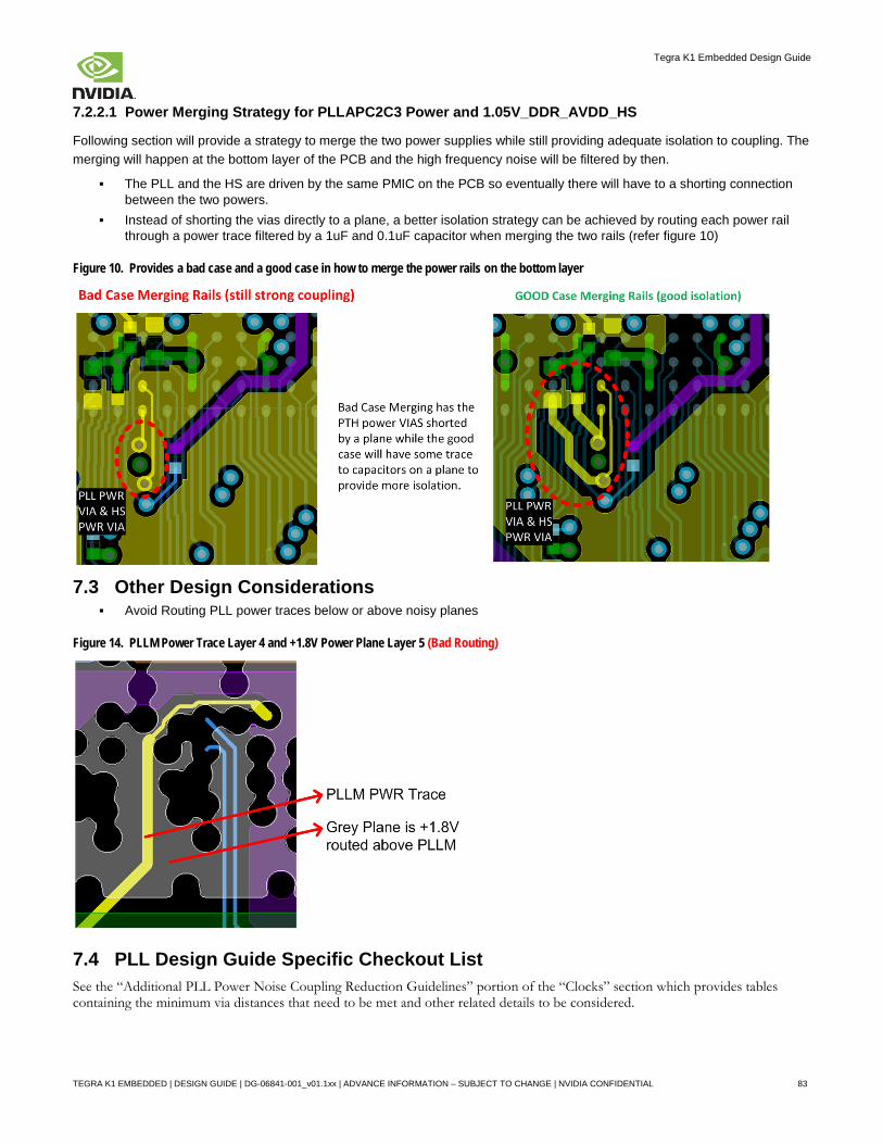
7.3 Other Design Considerations ...................................................................................................................................... 83 7.4 PLL Design Guide Specific Checkout List .................................................................................................................. 83
TEGRA K1 EMBEDDED | DESIGN GUIDE | DG-06841-001_v01.1xx | ADVANCE INFORMATION – SUBJECT TO CHANGE | NVIDIA CONFIDENTIAL 4
Tegra K1 Embedded Design Guide
1.0 INTRODUCTION
1.1 References Refer to the documents or models listed in Table 1 for more information. Use the latest revision of all documents at all times.
Table 1. List of Related Documents Document
1.2 Abbreviations and Definitions Table 2 lists abbreviations that may be used throughout this document and their definitions.
Table 2. Abbreviations and Definitions
Abbreviation Definition BT Bluetooth CEC Consumer Electronic Control DDR3L Double Data Rate DRAM, Third-generation eMMC Embedded MMC GNSS Global Navigation Satellite System GPS Global Positioning System HDMI High Definition Multimedia Interface HSIC High Speed Inter Chip Interface I2C Inter IC I2S Inter IC Sound Interface KBC Keyboard Controller LCD Liquid Crystal Display LDO Low Dropout (voltage regulator) LVDS Low Voltage Differential Signaling Interface MMC Multi-Media Card / High Speed MMC PCIe Peripheral Component Interconnect Express interface PCM Pulse Code Modulation PHY Physical Interface (i.e. USB PHY) PMC Power Management Controller PMU Power Management Unit RF Radio Frequency RTC Real Time Clock SATA Serial “AT” Attachment interface SDIO Secure Digital I/O Interface SPI Serial Peripheral Interface UART Universal Asynchronous Receiver-Transmitter ULPI UTMI+ Low Pin-count Interface USB Universal Serial Bus WLAN Wireless Local Area Network
TEGRA K1 EMBEDDED | DESIGN GUIDE | DG-06841-001_v01.1xx | ADVANCE INFORMATION – SUBJECT TO CHANGE | NVIDIA CONFIDENTIAL 5
Tegra K1 Embedded Design Guide
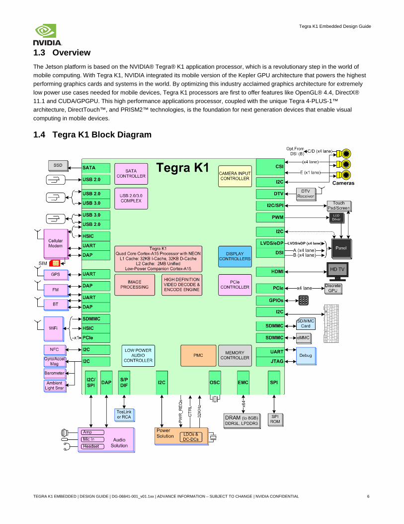
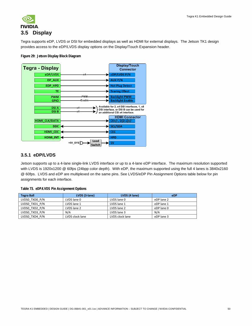
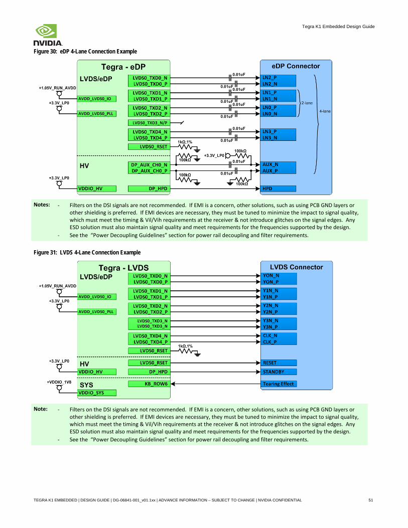
1.3 Overview The Jetson platform is based on the NVIDIA® Tegra® K1 application processor, which is a revolutionary step in the world of mobile computing. With Tegra K1, NVIDIA integrated its mobile version of the Kepler GPU architecture that powers the highest performing graphics cards and systems in the world. By optimizing this industry acclaimed graphics architecture for extremely low power use cases needed for mobile devices, Tegra K1 processors are first to offer features like OpenGL® 4.4, DirectX® 11.1 and CUDA/GPGPU. This high performance applications processor, coupled with the unique Tegra 4-PLUS-1™ architecture, DirectTouch™, and PRISM2™ technologies, is the foundation for next generation devices that enable visual computing in mobile devices.
1.4 Tegra K1 Block Diagram
TEGRA K1 EMBEDDED | DESIGN GUIDE | DG-06841-001_v01.1xx | ADVANCE INFORMATION – SUBJECT TO CHANGE | NVIDIA CONFIDENTIAL 6
Tegra K1 Embedded Design Guide
2.0 POWER
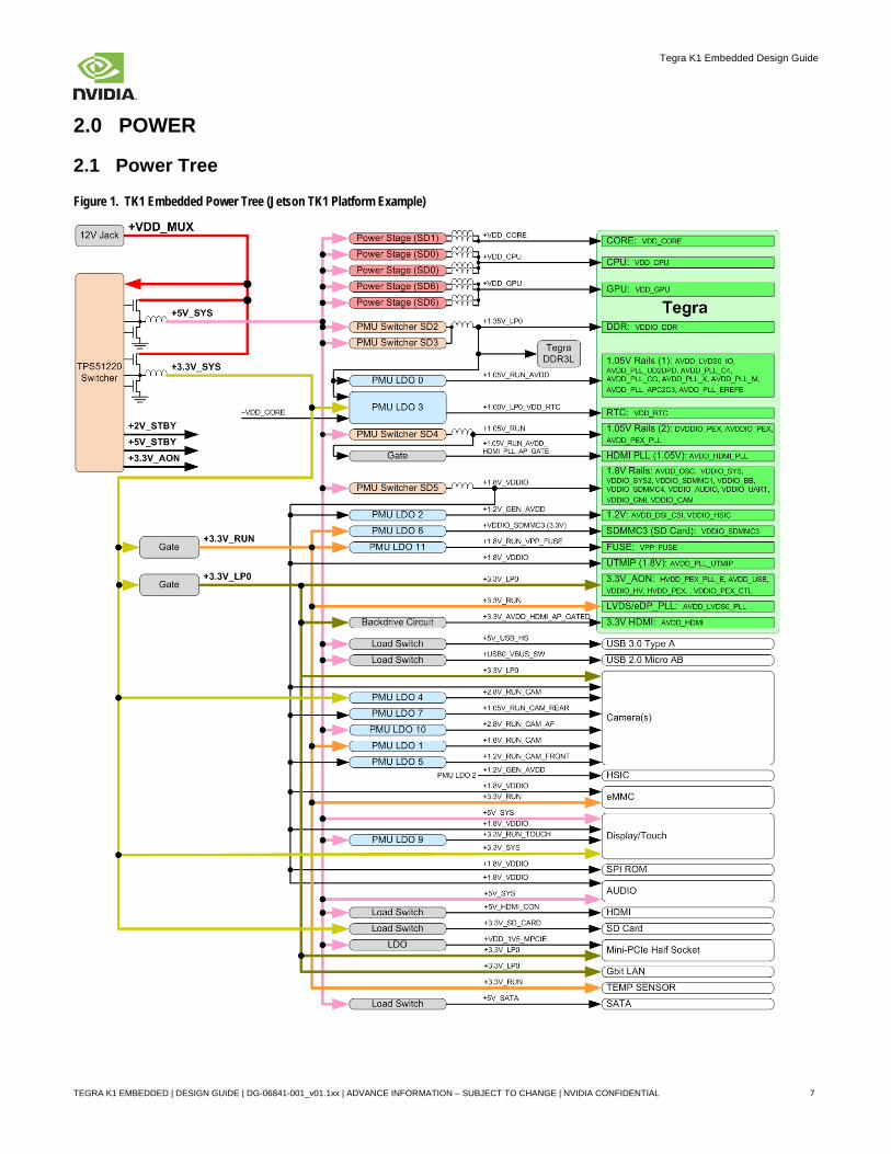
2.1 Power Tree
Figure 1. TK1 Embedded Power Tree (Jetson TK1 Platform Example)
TEGRA K1 EMBEDDED | DESIGN GUIDE | DG-06841-001_v01.1xx | ADVANCE INFORMATION – SUBJECT TO CHANGE | NVIDIA CONFIDENTIAL 7
Tegra K1 Embedded Design Guide
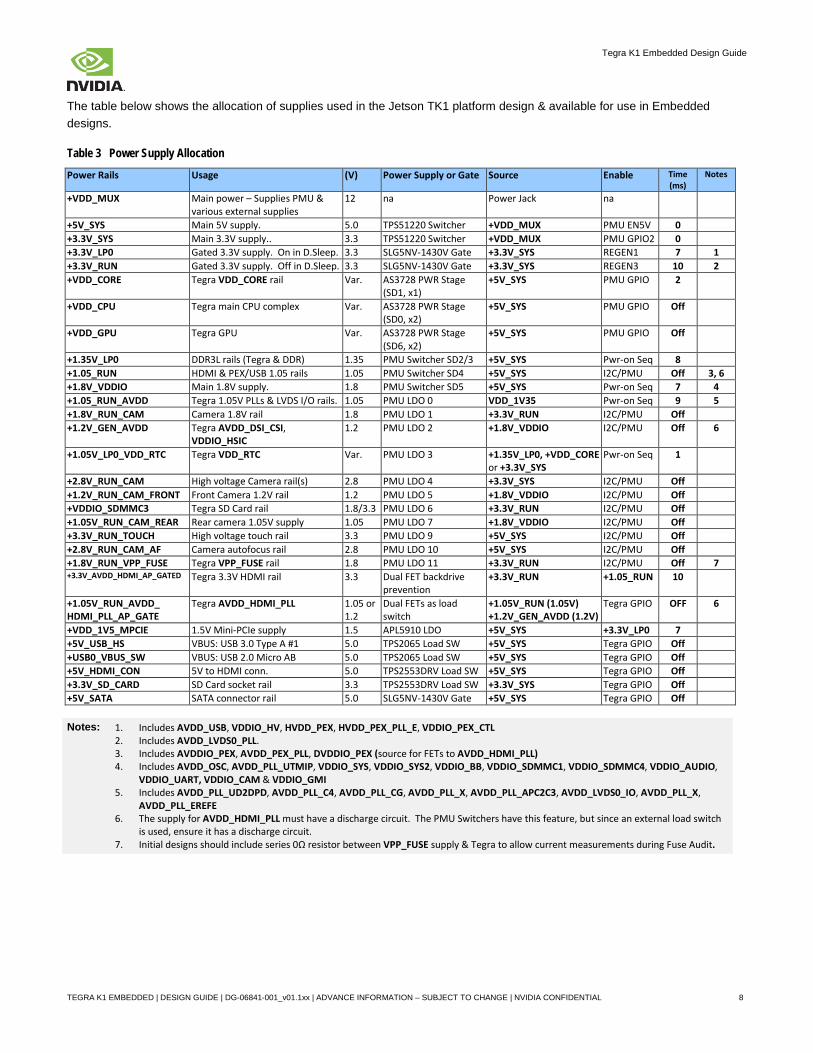
The table below shows the allocation of supplies used in the Jetson TK1 platform design & available for use in Embedded designs.
Table 3 Power Supply Allocation
Power Rails Usage (V) Power Supply or Gate Source Enable Time (ms)
Notes
+VDD_MUX Main power – Supplies PMU & various external supplies
12 na Power Jack na
+5V_SYS Main 5V supply. 5.0 TPS51220 Switcher +VDD_MUX PMU EN5V 0 +3.3V_SYS Main 3.3V supply.. 3.3 TPS51220 Switcher +VDD_MUX PMU GPIO2 0 +3.3V_LP0 Gated 3.3V supply. On in D.Sleep. 3.3 SLG5NV-1430V Gate +3.3V_SYS REGEN1 7 1 +3.3V_RUN Gated 3.3V supply. Off in D.Sleep. 3.3 SLG5NV-1430V Gate +3.3V_SYS REGEN3 10 2 +VDD_CORE Tegra VDD_CORE rail Var. AS3728 PWR Stage
(SD1, x1) +5V_SYS PMU GPIO 2
+VDD_CPU Tegra main CPU complex Var. AS3728 PWR Stage (SD0, x2)
+5V_SYS PMU GPIO Off
+VDD_GPU Tegra GPU Var. AS3728 PWR Stage (SD6, x2)
VDDIO_HSIC 1.2 PMU LDO 2 +1.8V_VDDIO I2C/PMU Off 6
+1.05V_LP0_VDD_RTC Tegra VDD_RTC Var. PMU LDO 3 +1.35V_LP0, +VDD_CORE or +3.3V_SYS
Pwr-on Seq 1
+2.8V_RUN_CAM High voltage Camera rail(s) 2.8 PMU LDO 4 +3.3V_SYS I2C/PMU Off +1.2V_RUN_CAM_FRONT Front Camera 1.2V rail 1.2 PMU LDO 5 +1.8V_VDDIO I2C/PMU Off +VDDIO_SDMMC3 Tegra SD Card rail 1.8/3.3 PMU LDO 6 +3.3V_RUN I2C/PMU Off +1.05V_RUN_CAM_REAR Rear camera 1.05V supply 1.05 PMU LDO 7 +1.8V_VDDIO I2C/PMU Off +3.3V_RUN_TOUCH High voltage touch rail 3.3 PMU LDO 9 +5V_SYS I2C/PMU Off +2.8V_RUN_CAM_AF Camera autofocus rail 2.8 PMU LDO 10 +5V_SYS I2C/PMU Off +1.8V_RUN_VPP_FUSE Tegra VPP_FUSE rail 1.8 PMU LDO 11 +3.3V_RUN I2C/PMU Off 7 +3.3V_AVDD_HDMI_AP_GATED Tegra 3.3V HDMI rail 3.3 Dual FET backdrive
prevention +3.3V_RUN +1.05_RUN 10
+1.05V_RUN_AVDD_ HDMI_PLL_AP_GATE
Tegra AVDD_HDMI_PLL 1.05 or 1.2
Dual FETs as load switch
+1.05V_RUN (1.05V) +1.2V_GEN_AVDD (1.2V)
Tegra GPIO OFF 6
+VDD_1V5_MPCIE 1.5V Mini-PCIe supply 1.5 APL5910 LDO +5V_SYS +3.3V_LP0 7 +5V_USB_HS VBUS: USB 3.0 Type A #1 5.0 TPS2065 Load SW +5V_SYS Tegra GPIO Off +USB0_VBUS_SW VBUS: USB 2.0 Micro AB 5.0 TPS2065 Load SW +5V_SYS Tegra GPIO Off +5V_HDMI_CON 5V to HDMI conn. 5.0 TPS2553DRV Load SW +5V_SYS Tegra GPIO Off +3.3V_SD_CARD SD Card socket rail 3.3 TPS2553DRV Load SW +3.3V_SYS Tegra GPIO Off +5V_SATA SATA connector rail 5.0 SLG5NV-1430V Gate +5V_SYS Tegra GPIO Off Notes: 1. Includes AVDD_USB, VDDIO_HV, HVDD_PEX, HVDD_PEX_PLL_E, VDDIO_PEX_CTL
2. Includes AVDD_LVDS0_PLL. 3. Includes AVDDIO_PEX, AVDD_PEX_PLL, DVDDIO_PEX (source for FETs to AVDD_HDMI_PLL) 4. Includes AVDD_OSC, AVDD_PLL_UTMIP, VDDIO_SYS, VDDIO_SYS2, VDDIO_BB, VDDIO_SDMMC1, VDDIO_SDMMC4, VDDIO_AUDIO,
AVDD_PLL_EREFE 6. The supply for AVDD_HDMI_PLL must have a discharge circuit. The PMU Switchers have this feature, but since an external load switch
is used, ensure it has a discharge circuit. 7. Initial designs should include series 0Ω resistor between VPP_FUSE supply & Tegra to allow current measurements during Fuse Audit.
TEGRA K1 EMBEDDED | DESIGN GUIDE | DG-06841-001_v01.1xx | ADVANCE INFORMATION – SUBJECT TO CHANGE | NVIDIA CONFIDENTIAL 8
Tegra K1 Embedded Design Guide
2.2 CPU, GPU, CORE & DDR Supply Considerations The total power solution for the CPU, GPU, CORE & DDR supplies must meet the requirements listed in the Tegra K1 Data Sheet including:
Voltage steps required by DVFS software Maximum EDP current Minimum voltage ramp rates
In addition, in order to meet the full EDP max current, care must be taken in selecting the critical components that make up each supply circuit. These components, including the PMU switcher or external regulators must meet the current requirements and the +/- 7% maximum tolerance allowed at the Tegra power balls including supply DC tolerance, ripple & voltage transients (variations in voltage caused by changes in load).
Impedance simulations should use all the output capacitors (large capacitor[s] just beyond DC-DC inductor), as source, and all the power pins as sinks.
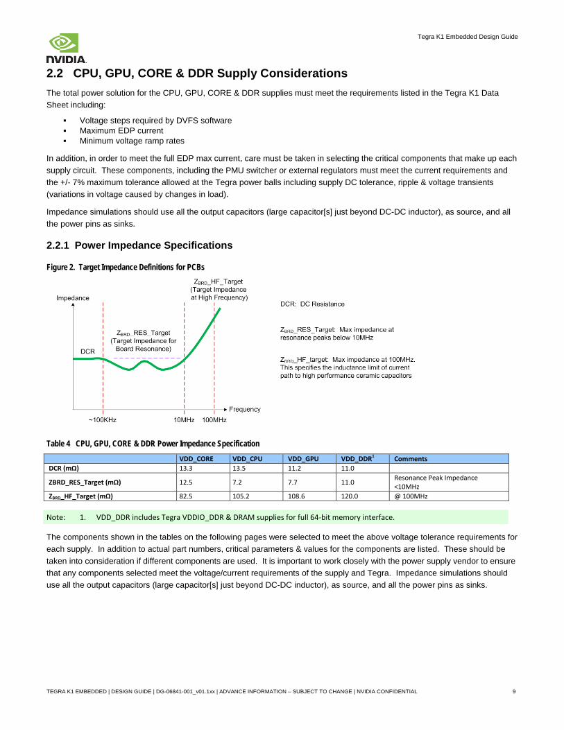
2.2.1 Power Impedance Specifications
Figure 2. Target Impedance Definitions for PCBs
Table 4 CPU, GPU, CORE & DDR Power Impedance Specification
Note: 1. VDD_DDR includes Tegra VDDIO_DDR & DRAM supplies for full 64-bit memory interface.
The components shown in the tables on the following pages were selected to meet the above voltage tolerance requirements for each supply. In addition to actual part numbers, critical parameters & values for the components are listed. These should be taken into consideration if different components are used. It is important to work closely with the power supply vendor to ensure that any components selected meet the voltage/current requirements of the supply and Tegra. Impedance simulations should use all the output capacitors (large capacitor[s] just beyond DC-DC inductor), as source, and all the power pins as sinks.
TEGRA K1 EMBEDDED | DESIGN GUIDE | DG-06841-001_v01.1xx | ADVANCE INFORMATION – SUBJECT TO CHANGE | NVIDIA CONFIDENTIAL 9
Tegra K1 Embedded Design Guide
Table 5 Critical VDD_CPU Switcher Components Recommendations (Three Power Stages)
Table 6 Critical VDD_GPU Switcher Components Recommendations (Two Power Stages)
Table 7 Critical VDD_CORE Switcher Components Recommendations (One Power Stage)
Table 8. Basic Tegra Power Control Connections
Ball Name Type Termination (typical) Description CLK_32K_IN I 32.768kHz Clock: input for 32kHz clock used by RTC & PMC blocks SYS_RESET_N I System Reset: Reset input for Tegra PWR_I2C_SCL/SDA O/B 1KΩ pull-up resistor to VDDIO_SYS. Power I2C: Connect to PMU. CORE_PWR_REQ O Core Power Request: Connect to CORE_PWRREQ on PMU CPU_PWR_REQ O CPU Power Request: Connect to CPU_PWRREQ on PMU PWR_INT I Power Interrupt: Connect to XINT pin on PMU
Components MFG MFG Part # Qty Parameter Symbol Conditions Value Units PMIC (Ctrlr) AMS AS3722 1 Switching Frequency f 1.35 MHz 2 phase per Pwr Stage AMS AS3728 3 Max Current I 2x10 A Inductor TDK SPM4015-R68M 6 Inductance L 0.68 uH
DC Resistance DCR 32.7 mΩ Size LxWxH 4.4x4.1x1.5 mm RMS Current Irms 40C rise 4.7 A Saturation Current Isat 30% drop 8 A
Output Capacitor
Taiyo Yuden JMK212BJ476MG-T 4 per Power Stage)
Data Sheet Capacitance C 47 uF Size LxW 0805 mm Dielectric X5R Code Rated Voltage V 6.3 V
Input Capacitor
Taiyo Yuden TMK316BJ106KD-TD 4 per Power Stage)
Data Sheet Capacitance C 10 uF Size LxW 3.5 mm Dielectric X5R Code Rated Voltage V 25 V
PCB Routing TBD mΩ
Components MFG MFG Part # Qty Parameter Symbol Conditions Value Units PMIC (Ctrlr) AMS AS3722 1 Switching Frequency f 1.35 MHz 2 phase per Pwr Stage AMS AS3728 2 Max Current I 10 A Inductor TDK SPM4015-R68M 4 Inductance L 0.68 uH
DC Resistance DCR 32.7 mΩ Size LxWxH 4.4x4.1x1.5 mm RMS Current Irms 40C rise 4.7 A Saturation Current Isat 30% drop 8 A
Output Capacitor
Taiyo Yuden JMK212BJ476MG-T 3 per Power Stage)
Data Sheet Capacitance C 47 uF Size LxW 0805 mm Dielectric X5R Code Rated Voltage V 6.3 V
Input Capacitor
Taiyo Yuden TMK316BJ106KD-TD 4 per Power Stage)
Data Sheet Capacitance C 10 uF Size LxW 1206 mm Dielectric X5R Code Rated Voltage V 25 V
PCB Routing TBD mΩ
Components MFG MFG Part # Qty Parameter Symbol Conditions Value Units PMIC (Ctrlr) AMS AS3722 1 Switching Frequency f 1.35 MHz 2 phase per Pwr Stage AMS AS3728 1 Max Current I 10 A Inductor TDK SPM4015-R68M 2 Inductance L 0.68 uH
DC Resistance DCR 32.7 mΩ Size LxWxH 4.4x4.1x1.5 mm RMS Current Irms 40C rise 4.7 A Saturation Current Isat 30% drop 8 A
Output Capacitor
Taiyo Yuden JMK212BJ476MG-T 3 Data Sheet Capacitance C 47 uF Size LxW 0805 mm Dielectric X5R Code Rated Voltage V 6.3 V
Input Capacitor
Taiyo Yuden TMK316BJ106KD-TD 4 Data Sheet Capacitance C 10 uF Size LxW 1206 mm Dielectric X5R Code Rated Voltage V 25 V
PCB Routing TBD mΩ
TEGRA K1 EMBEDDED | DESIGN GUIDE | DG-06841-001_v01.1xx | ADVANCE INFORMATION – SUBJECT TO CHANGE | NVIDIA CONFIDENTIAL 10
Tegra K1 Embedded Design Guide
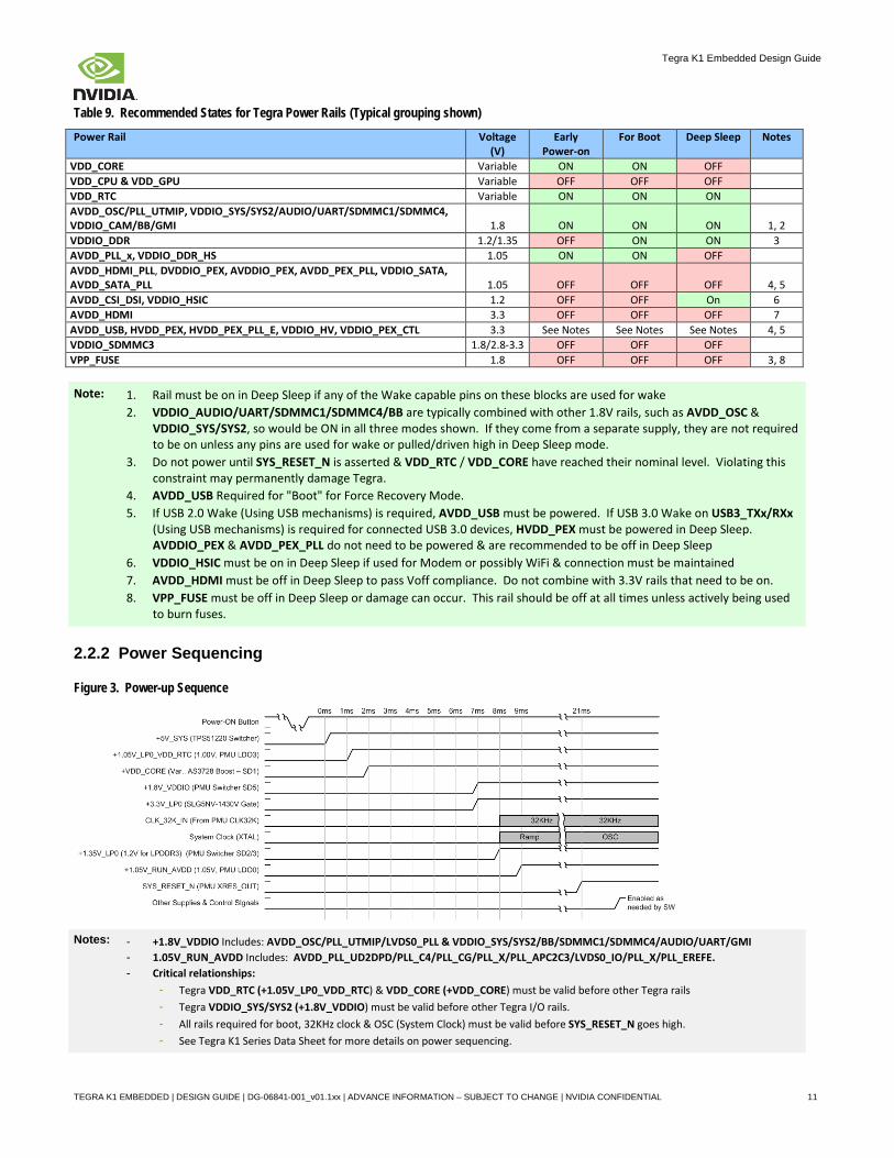
Table 9. Recommended States for Tegra Power Rails (Typical grouping shown)
Power Rail Voltage (V)
Early Power-on
For Boot Deep Sleep Notes
VDD_CORE Variable ON ON OFF VDD_CPU & VDD_GPU Variable OFF OFF OFF VDD_RTC Variable ON ON ON AVDD_OSC/PLL_UTMIP, VDDIO_SYS/SYS2/AUDIO/UART/SDMMC1/SDMMC4, VDDIO_CAM/BB/GMI 1.8 ON ON ON 1, 2 VDDIO_DDR 1.2/1.35 OFF ON ON 3 AVDD_PLL_x, VDDIO_DDR_HS 1.05 ON ON OFF AVDD_HDMI_PLL, DVDDIO_PEX, AVDDIO_PEX, AVDD_PEX_PLL, VDDIO_SATA, AVDD_SATA_PLL 1.05 OFF OFF OFF 4, 5 AVDD_CSI_DSI, VDDIO_HSIC 1.2 OFF OFF On 6 AVDD_HDMI 3.3 OFF OFF OFF 7 AVDD_USB, HVDD_PEX, HVDD_PEX_PLL_E, VDDIO_HV, VDDIO_PEX_CTL 3.3 See Notes See Notes See Notes 4, 5 VDDIO_SDMMC3 1.8/2.8-3.3 OFF OFF OFF VPP_FUSE 1.8 OFF OFF OFF 3, 8
Note: 1. Rail must be on in Deep Sleep if any of the Wake capable pins on these blocks are used for wake 2. VDDIO_AUDIO/UART/SDMMC1/SDMMC4/BB are typically combined with other 1.8V rails, such as AVDD_OSC &
VDDIO_SYS/SYS2, so would be ON in all three modes shown. If they come from a separate supply, they are not required to be on unless any pins are used for wake or pulled/driven high in Deep Sleep mode.
3. Do not power until SYS_RESET_N is asserted & VDD_RTC / VDD_CORE have reached their nominal level. Violating this constraint may permanently damage Tegra.
4. AVDD_USB Required for "Boot" for Force Recovery Mode. 5. If USB 2.0 Wake (Using USB mechanisms) is required, AVDD_USB must be powered. If USB 3.0 Wake on USB3_TXx/RXx
(Using USB mechanisms) is required for connected USB 3.0 devices, HVDD_PEX must be powered in Deep Sleep. AVDDIO_PEX & AVDD_PEX_PLL do not need to be powered & are recommended to be off in Deep Sleep
6. VDDIO_HSIC must be on in Deep Sleep if used for Modem or possibly WiFi & connection must be maintained 7. AVDD_HDMI must be off in Deep Sleep to pass Voff compliance. Do not combine with 3.3V rails that need to be on. 8. VPP_FUSE must be off in Deep Sleep or damage can occur. This rail should be off at all times unless actively being used
- Tegra VDD_RTC (+1.05V_LP0_VDD_RTC) & VDD_CORE (+VDD_CORE) must be valid before other Tegra rails - Tegra VDDIO_SYS/SYS2 (+1.8V_VDDIO) must be valid before other Tegra I/O rails. - All rails required for boot, 32KHz clock & OSC (System Clock) must be valid before SYS_RESET_N goes high. - See Tegra K1 Series Data Sheet for more details on power sequencing.
TEGRA K1 EMBEDDED | DESIGN GUIDE | DG-06841-001_v01.1xx | ADVANCE INFORMATION – SUBJECT TO CHANGE | NVIDIA CONFIDENTIAL 11
Tegra K1 Embedded Design Guide
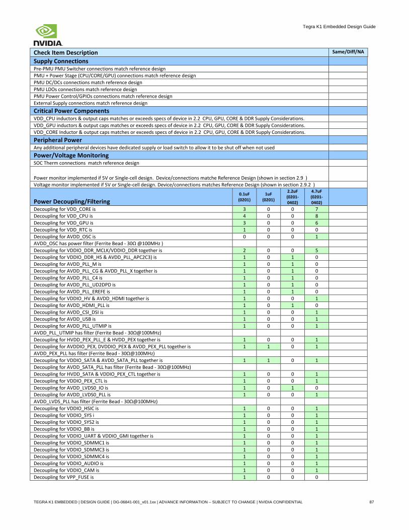
2.3 Power Decoupling Guidelines See Checklist table at end of document for Decoupling requirements.
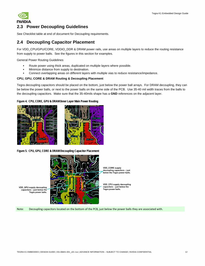
2.4 Decoupling Capacitor Placement For VDD_CPU/GPU/CORE, VDDIO_DDR & DRAM power rails, use areas on multiple layers to reduce the routing resistance from supply to power balls. See the figures in this section for examples.
General Power Routing Guidelines
Route power using thick areas, duplicated on multiple layers where possible. Minimize distance from supply to destination. Connect overlapping areas on different layers with multiple vias to reduce resistance/impedance.
CPU, GPU, CORE & DRAM Routing & Decoupling Placement
Tegra decoupling capacitors should be placed on the bottom, just below the power ball arrays. For DRAM decoupling, they can be below the power balls, or next to the power balls on the same side of the PCB. Use 35-40 mil width traces from the balls to the decoupling capacitors. Make sure that the 35-40mils shape has a GND references on the adjacent layer.
Figure 4. CPU, CORE, GPU & DRAM Inner Layer Main Power Routing
Figure 5. CPU, GPU, CORE & DRAM Decoupling Capacitor Placement
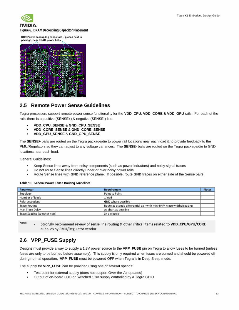
Note: Decoupling capacitors located on the bottom of the PCB, just below the power balls they are associated with.
TEGRA K1 EMBEDDED | DESIGN GUIDE | DG-06841-001_v01.1xx | ADVANCE INFORMATION – SUBJECT TO CHANGE | NVIDIA CONFIDENTIAL 12
Tegra K1 Embedded Design Guide
Figure 6. DRAM Decoupling Capacitor Placement
2.5 Remote Power Sense Guidelines Tegra processors support remote power sense functionality for the VDD_CPU, VDD_CORE & VDD_GPU rails. For each of the rails there is a positive (SENSE+) & negative (SENSE-) line.
The SENSE+ balls are routed on the Tegra package/die to power rail locations near each load & to provide feedback to the PMU/Regulators so they can adjust to any voltage variances. The SENSE- balls are routed on the Tegra package/die to GND locations near each load.
General Guidelines:
Keep Sense lines away from noisy components (such as power inductors) and noisy signal traces Do not route Sense lines directly under or over noisy power rails. Route Sense lines with GND reference plane. If possible, route GND traces on either side of the Sense pairs
Table 10. General Power Sense Routing Guidelines
Parameter Requirement Notes Topology Point to Point Number of loads 1 load Reference plane GND where possible Trace Routing Route as pseudo differential pair with min 4/4/4 trace widths/spacing Max Trace Delay As short as possible Trace Spacing (to other nets) 3x dielectric
Note: - Strongly recommend review of sense line routing & other critical items related to VDD_CPU/GPU/CORE
supplies by PMU/Regulator vendor
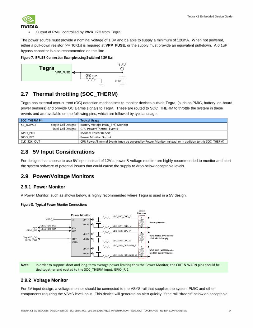
2.6 VPP_FUSE Supply Designs must provide a way to supply a 1.8V power source to the VPP_FUSE pin on Tegra to allow fuses to be burned (unless fuses are only to be burned before assembly). This supply is only required when fuses are burned and should be powered off during normal operation. VPP_FUSE must be powered OFF when Tegra is in Deep Sleep mode.
The supply for VPP_FUSE can be provided using one of several options:
Test point for external supply (does not support Over-the-Air updates) Output of on-board LDO or Switched 1.8V supply controlled by a Tegra GPIO
TEGRA K1 EMBEDDED | DESIGN GUIDE | DG-06841-001_v01.1xx | ADVANCE INFORMATION – SUBJECT TO CHANGE | NVIDIA CONFIDENTIAL 13
Tegra K1 Embedded Design Guide
Output of PMU, controlled by PWR_I2C from Tegra
The power source must provide a nominal voltage of 1.8V and be able to supply a minimum of 120mA. When not powered, either a pull-down resistor (<= 10KΩ) is required at VPP_FUSE, or the supply must provide an equivalent pull-down. A 0.1uF bypass capacitor is also recommended on this line.
Figure 7. EFUSE Connection Example using Switched 1.8V Rail
2.7 Thermal throttling (SOC_THERM) Tegra has external over-current (OC) detection mechanisms to monitor devices outside Tegra, (such as PMIC, battery, on-board power sensors) and provide OC alarms signals to Tegra. These are routed to SOC_THERM to throttle the system in these events and are available on the following pins, which are followed by typical usage.
Battery Voltage (VDD_SYS) Monitor GPU Power/Thermal Events
GPIO_PK0 Modem Power Report GPIO_PJ2 Power Monitor Output CLK_32K_OUT CPU Power/Thermal Events (may be covered by Power Monitor instead, or in addition to this SOC_THERM)
2.8 5V Input Considerations For designs that choose to use 5V input instead of 12V a power & voltage monitor are highly recommended to monitor and alert the system software of potential issues that could cause the supply to drop below acceptable levels.
2.9 Power/Voltage Monitors
2.9.1 Power Monitor
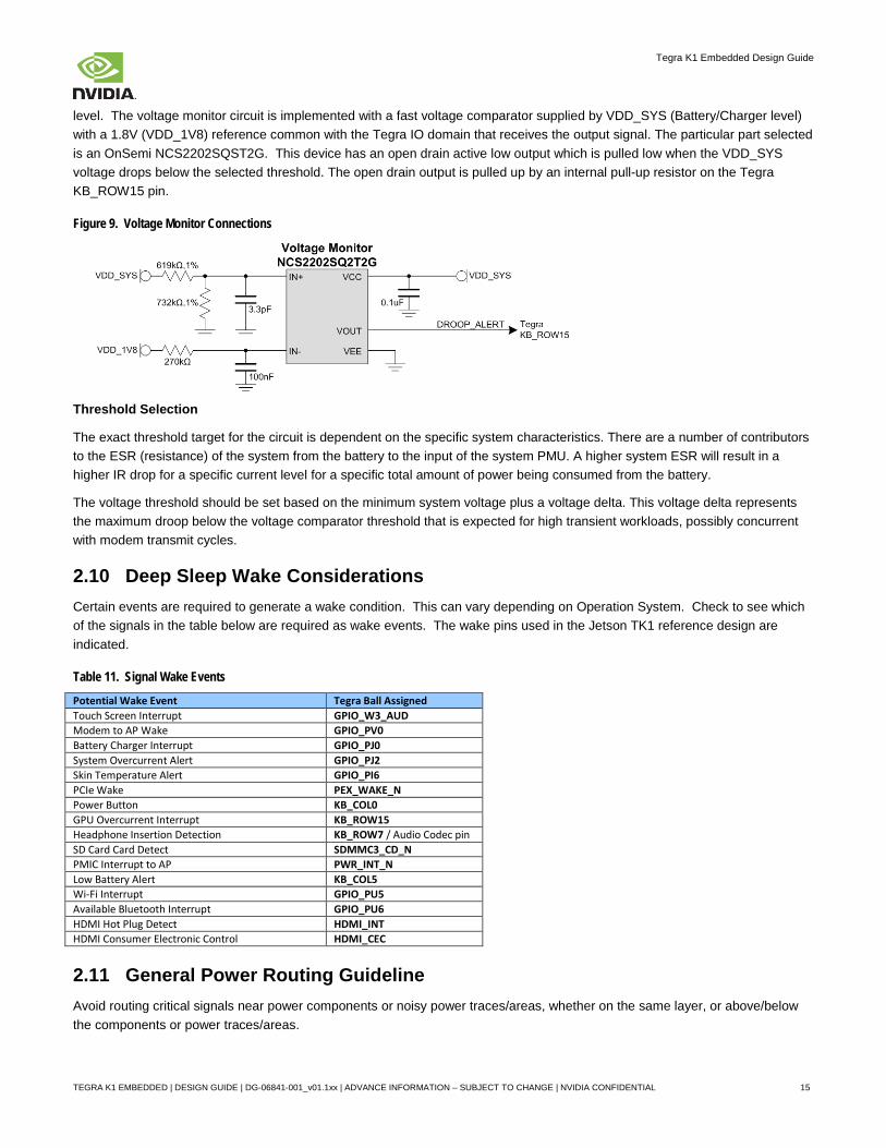
A Power Monitor, such as shown below, is highly recommended where Tegra is used in a 5V design.
Figure 8. Typical Power Monitor Connections
Note: In order to support short and long-term average power limiting thru the Power Monitor, the CRIT & WARN pins should be tied together and routed to the SOC_THERM input, GPIO_PJ2
2.9.2 Voltage Monitor
For 5V input design, a voltage monitor should be connected to the VSYS rail that supplies the system PMIC and other components requiring the VSYS level input. This device will generate an alert quickly, if the rail “droops” below an acceptable
TEGRA K1 EMBEDDED | DESIGN GUIDE | DG-06841-001_v01.1xx | ADVANCE INFORMATION – SUBJECT TO CHANGE | NVIDIA CONFIDENTIAL 14
Tegra K1 Embedded Design Guide
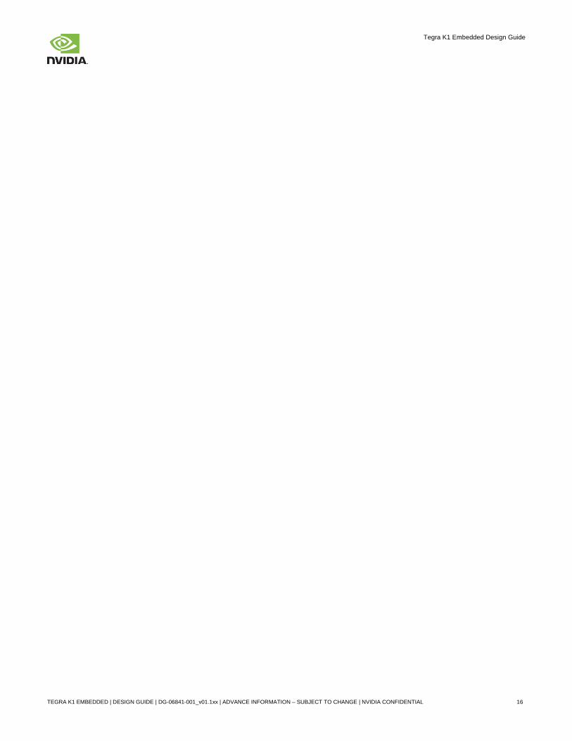
level. The voltage monitor circuit is implemented with a fast voltage comparator supplied by VDD_SYS (Battery/Charger level) with a 1.8V (VDD_1V8) reference common with the Tegra IO domain that receives the output signal. The particular part selected is an OnSemi NCS2202SQST2G. This device has an open drain active low output which is pulled low when the VDD_SYS voltage drops below the selected threshold. The open drain output is pulled up by an internal pull-up resistor on the Tegra KB_ROW15 pin.
Figure 9. Voltage Monitor Connections
Threshold Selection
The exact threshold target for the circuit is dependent on the specific system characteristics. There are a number of contributors to the ESR (resistance) of the system from the battery to the input of the system PMU. A higher system ESR will result in a higher IR drop for a specific current level for a specific total amount of power being consumed from the battery.
The voltage threshold should be set based on the minimum system voltage plus a voltage delta. This voltage delta represents the maximum droop below the voltage comparator threshold that is expected for high transient workloads, possibly concurrent with modem transmit cycles.
2.10 Deep Sleep Wake Considerations Certain events are required to generate a wake condition. This can vary depending on Operation System. Check to see which of the signals in the table below are required as wake events. The wake pins used in the Jetson TK1 reference design are indicated.
Table 11. Signal Wake Events
Potential Wake Event Tegra Ball Assigned Touch Screen Interrupt GPIO_W3_AUD Modem to AP Wake GPIO_PV0 Battery Charger Interrupt GPIO_PJ0 System Overcurrent Alert GPIO_PJ2 Skin Temperature Alert GPIO_PI6 PCIe Wake PEX_WAKE_N Power Button KB_COL0 GPU Overcurrent Interrupt KB_ROW15 Headphone Insertion Detection KB_ROW7 / Audio Codec pin SD Card Card Detect SDMMC3_CD_N PMIC Interrupt to AP PWR_INT_N Low Battery Alert KB_COL5 Wi-Fi Interrupt GPIO_PU5 Available Bluetooth Interrupt GPIO_PU6 HDMI Hot Plug Detect HDMI_INT HDMI Consumer Electronic Control HDMI_CEC
2.11 General Power Routing Guideline Avoid routing critical signals near power components or noisy power traces/areas, whether on the same layer, or above/below the components or power traces/areas.
TEGRA K1 EMBEDDED | DESIGN GUIDE | DG-06841-001_v01.1xx | ADVANCE INFORMATION – SUBJECT TO CHANGE | NVIDIA CONFIDENTIAL 15
Tegra K1 Embedded Design Guide
TEGRA K1 EMBEDDED | DESIGN GUIDE | DG-06841-001_v01.1xx | ADVANCE INFORMATION – SUBJECT TO CHANGE | NVIDIA CONFIDENTIAL 16
Tegra K1 Embedded Design Guide
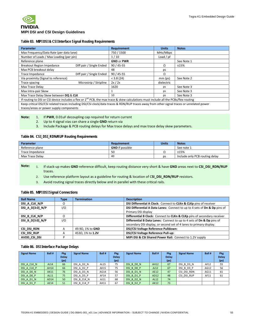
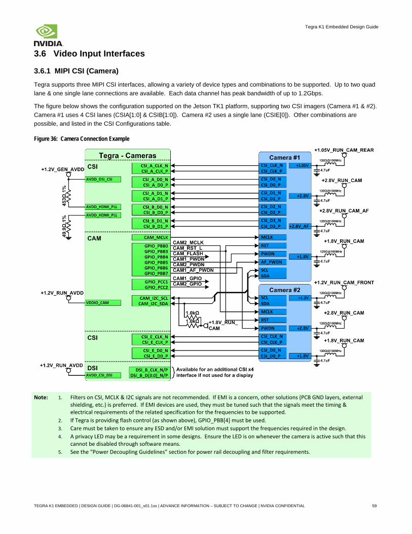
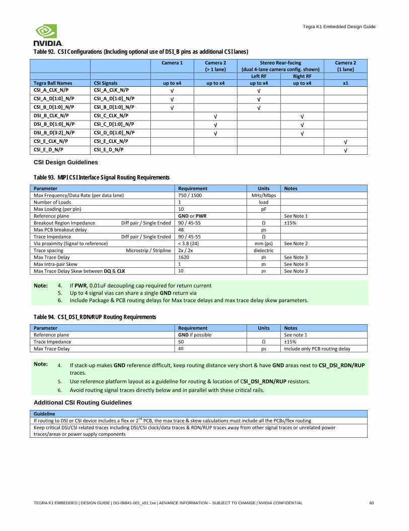
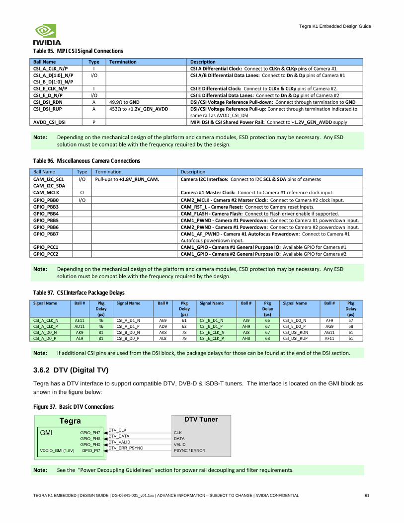
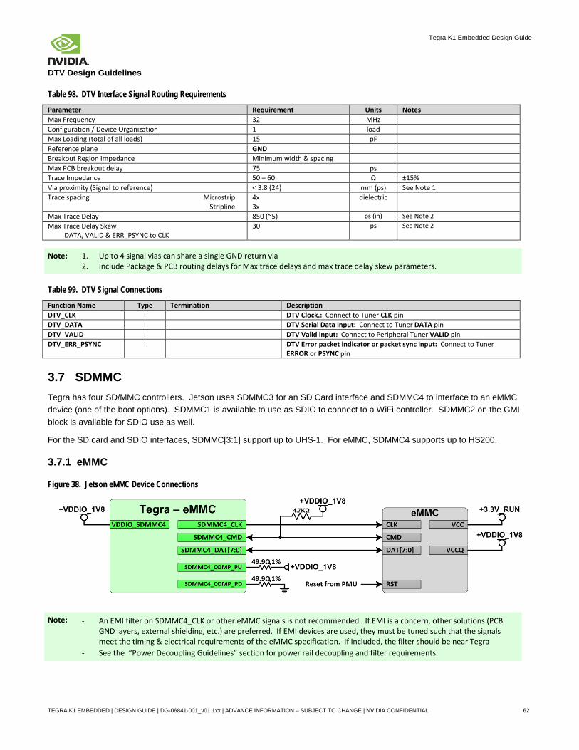
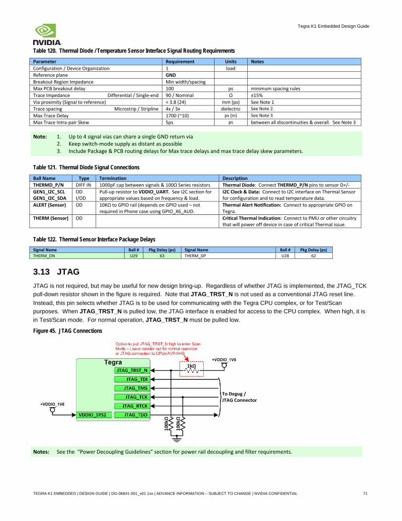
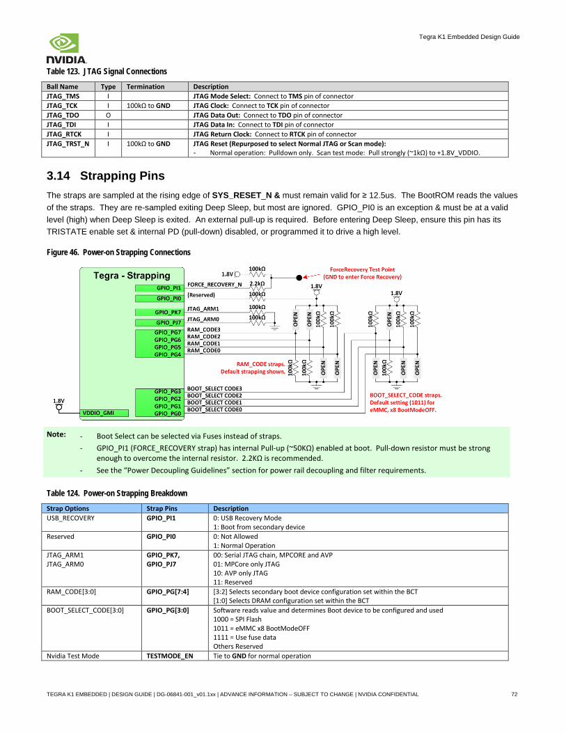
3.0 INTERFACE ROUTING GUIDELINES
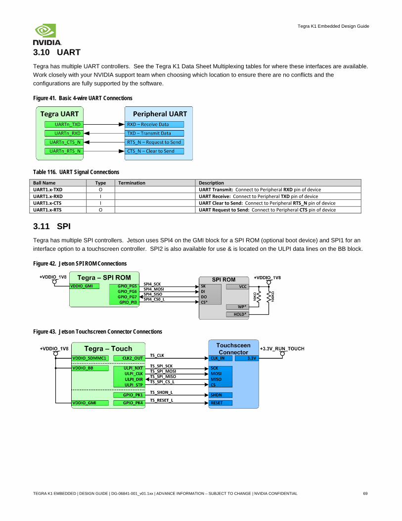
3.1 Overview This chapter contains the PCB routing and other guidelines for the following Tegra interfaces
Clocks DSI SDMMC Strapping Pins DRAM LVDS I2S Thermal Diode USB eDP I2C PCIe HDMI SPI SATA CSI UART HSIC DTV JTAG Note: - Unless otherwise noted, all resistor values are ±5% & trace impedance values are ±15%
Signal Name Conventions
The following conventions are used in describing the signals for Tegra:
Signal names use a mnemonic to represent the function of the signal (i.e. Secure Digital Interface #3 CMD signal is SDMMC3_CMD), written in bold to distinguish it from other text. Active low signals usually have an underscore followed by capital N (_N) after the name (i.e. SYS_RESET_N). Differential signals are identified as a pair with the same names that end with _P and _N or just P and N (for positive and negative, respectively). For example, USB1_DP and USB1_DN indicate a differential signal pair.
I/O Type The signal I/O type is represented as a code to indicate the operational characteristics of the signal. The table below lists the I/O codes used in the signal description tables.
Table 12. Signal Type Codes Code Definition A Analog DIFF I/O Bidirectional Differential Input/Output DIFF IN Differential Input DIFF OUT Differential Output I/O Bidirectional Input/Output I Input O Output OD Open Drain Output I/OD Bidirectional Input / Open Drain Output P Power
General SFIO (Special Function IO) & GPIO (General Purpose IO) selection.
The SFIO and GPIO usage should match those used on Jetson TK1, or alternative “Use-case” options shown in the Jetson TK1 Pinmux spreadsheet.
Routing Guideline Format
The routing guidelines have the following format to specify how a signal should be routed.
Breakout traces are traces routed from BGA ball either to a point beyond the ball array, or to another layer where full normal spacing guidelines can be met. Breakout trace delay limited to 500 mils unless otherwise specified.
After breakout, signal should be routed according to specified impedance for differential, single-ended, or both (for example: HDMI). Trace spacing to other signals also specified.
Follow max & min trace delays where specified. Trace delays are typically shown in mm or in terms of signal delay in pico-seconds (ps) or both. - For differential signals, trace spacing to other signals must be larger of specified × dielectric height or inter-pair
spacing - Spacing to other signals/pairs cannot be smaller than spacing between complementary signals (intra-pair). - Total trace delay depends on signal velocity which is different between outer (microstrip) & inner (stripline) layers
of a PCB.
TEGRA K1 EMBEDDED | DESIGN GUIDE | DG-06841-001_v01.1xx | ADVANCE INFORMATION – SUBJECT TO CHANGE | NVIDIA CONFIDENTIAL 17
Tegra K1 Embedded Design Guide
Signal Routing Conventions
Throughout this document, the following signal routing conventions are used:
SE Impedance (/ Diff Impedance) at x Dielectric Height Spacing
Single-ended (SE) impedance of trace (along with differential impedance for diff pairs) is achieved by spacing requirement. Spacing is multiple of dielectric height. Dielectric height is typically different for microstrip & stripline. Note: 1 mil = 1/1000th of an inch.
Note: Trace spacing requirement applies to SE traces or differential pairs to other SE traces or differential pairs. It does not apply to traces making up a differential pair. For this case, spacing/trace widths are chosen to meet differential impedance requirement.
General Routing Guidelines
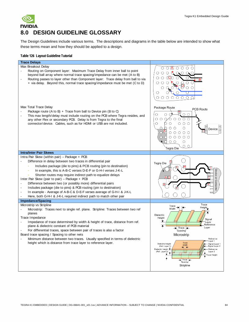
Pay close attention when routing high speed interfaces, such as DDR3L/LPDDR3, HDMI, USB/HSIC or DSI/CSI. Each of these interfaces has strict routing rules for the trace impedance, width, spacing, total delay, and delay/flight time matching. The following guidelines provide an overview of the routing guidelines and notations used in this document.
Controlled Impedance Each interface has different trace impedance requirements & spacing to other traces. It is up to designer to calculate trace width & spacing required to achieve specified single-ended (SE) & differential (Diff) impedances.
Max Trace Lengths/Delays Trace lengths/delays should include main PCB routing (where Tegra resides) and any additional routing on a Flex/ secondary PCB segment connected to main PCB. The max length/delay should be from Tegra to the actual connector (i.e. USB, HDMI, SD Card, etc.) or device (i.e. onboard USB device, Display driver IC, camera imager IC, etc.)
Trace Delay/Flight Time Matching Signal flight time is the time it takes for a signal to propagate from one end (driver) to other end (receiver). One way to get same flight time for signal within signal group is to match trace lengths within specified delay in the signal group. - Except for DRAM or if otherwise stated, always include Tegra substrate trace delay or propagation delay in all
trace delay or flight-time matching calculations. - Total trace delay = substrate trace delay + board trace delay. Do not exceed maximum trace delay specified. - For six layers or more, it is recommended to match trace delays based on flight time of signals. For example,
outer-layer signal velocity could be 150psi (ps/inch) & inner-layer 180psi. If one signal is routed 10 inches on outer layer & second signal is routed 10 inches in inner layer, difference in flight time between two signals will be 300ps! That is a big difference if required matching is 15ps (trace delay matching). To fix this, inner trace needs to be 1.7 inches shorter or outer trace needs to be 2 inches longer.
- In this design guide, terms such as intra-pair & inter-pair are used when describing differential pair delay. Intra-pair refers to matching traces within differential pair (for example, true to complement trace matching). Inter-pair matching refers to matching differential pairs average delays to other differential pairs average delays.
General PCB Routing Guidelines
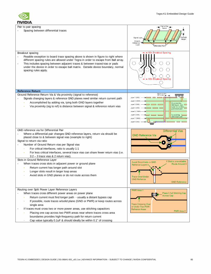
For GSSG stackup to minimize crosstalk, signal should be routed in such a way that they are not on top of each other in two routing layers (see diagram to right)
Do not route other signals or power traces/areas directly under or over critical high-speed interface signals.
TEGRA K1 EMBEDDED | DESIGN GUIDE | DG-06841-001_v01.1xx | ADVANCE INFORMATION – SUBJECT TO CHANGE | NVIDIA CONFIDENTIAL 18
Tegra K1 Embedded Design Guide
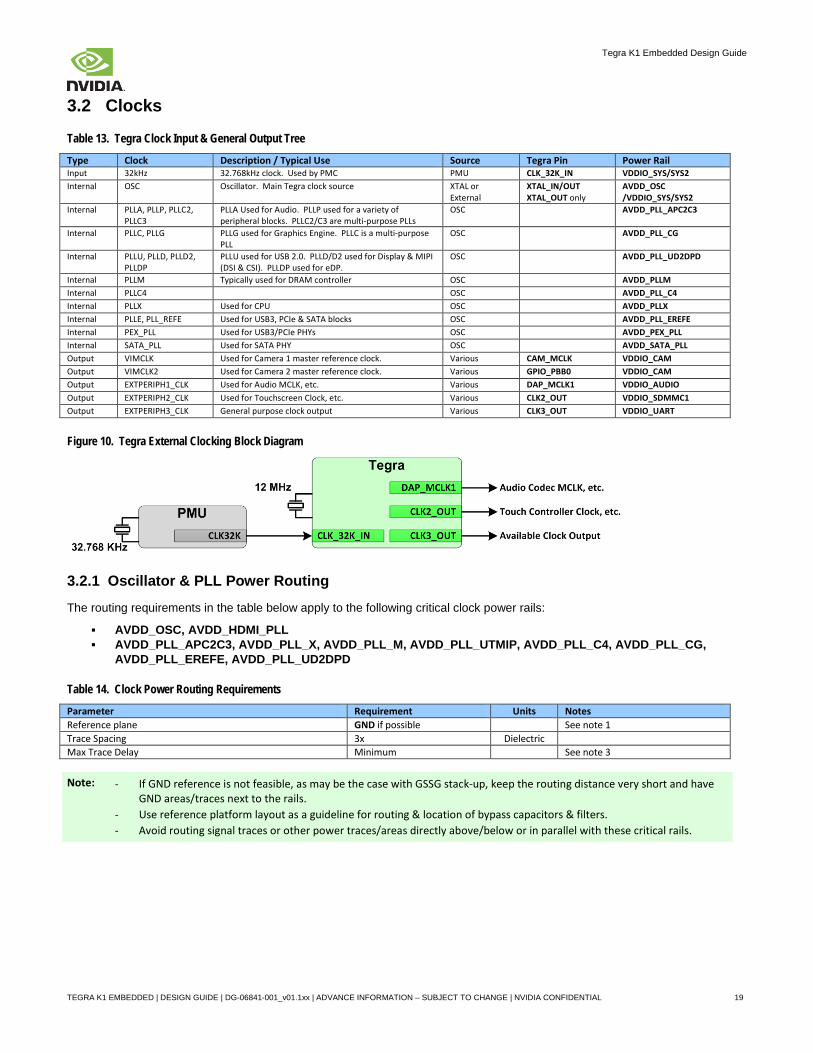
3.2 Clocks
Table 13. Tegra Clock Input & General Output Tree
Type Clock Description / Typical Use Source Tegra Pin Power Rail Input 32kHz 32.768kHz clock. Used by PMC PMU CLK_32K_IN VDDIO_SYS/SYS2 Internal OSC Oscillator. Main Tegra clock source XTAL or
External XTAL_IN/OUT XTAL_OUT only
AVDD_OSC /VDDIO_SYS/SYS2
Internal PLLA, PLLP, PLLC2, PLLC3
PLLA Used for Audio. PLLP used for a variety of peripheral blocks. PLLC2/C3 are multi-purpose PLLs
OSC AVDD_PLL_APC2C3
Internal PLLC, PLLG PLLG used for Graphics Engine. PLLC is a multi-purpose PLL
OSC AVDD_PLL_CG
Internal PLLU, PLLD, PLLD2, PLLDP
PLLU used for USB 2.0. PLLD/D2 used for Display & MIPI (DSI & CSI). PLLDP used for eDP.
OSC AVDD_PLL_UD2DPD
Internal PLLM Typically used for DRAM controller OSC AVDD_PLLM Internal PLLC4 OSC AVDD_PLL_C4 Internal PLLX Used for CPU OSC AVDD_PLLX Internal PLLE, PLL_REFE Used for USB3, PCIe & SATA blocks OSC AVDD_PLL_EREFE Internal PEX_PLL Used for USB3/PCIe PHYs OSC AVDD_PEX_PLL Internal SATA_PLL Used for SATA PHY OSC AVDD_SATA_PLL Output VIMCLK Used for Camera 1 master reference clock. Various CAM_MCLK VDDIO_CAM Output VIMCLK2 Used for Camera 2 master reference clock. Various GPIO_PBB0 VDDIO_CAM Output EXTPERIPH1_CLK Used for Audio MCLK, etc. Various DAP_MCLK1 VDDIO_AUDIO Output EXTPERIPH2_CLK Used for Touchscreen Clock, etc. Various CLK2_OUT VDDIO_SDMMC1 Output EXTPERIPH3_CLK General purpose clock output Various CLK3_OUT VDDIO_UART
Figure 10. Tegra External Clocking Block Diagram
3.2.1 Oscillator & PLL Power Routing
The routing requirements in the table below apply to the following critical clock power rails:
Parameter Requirement Units Notes Reference plane GND if possible See note 1 Trace Spacing 3x Dielectric Max Trace Delay Minimum See note 3
Note: - If GND reference is not feasible, as may be the case with GSSG stack-up, keep the routing distance very short and have GND areas/traces next to the rails.
- Use reference platform layout as a guideline for routing & location of bypass capacitors & filters. - Avoid routing signal traces or other power traces/areas directly above/below or in parallel with these critical rails.
TEGRA K1 EMBEDDED | DESIGN GUIDE | DG-06841-001_v01.1xx | ADVANCE INFORMATION – SUBJECT TO CHANGE | NVIDIA CONFIDENTIAL 19
Tegra K1 Embedded Design Guide
3.2.2 Additional PLL Power Noise Coupling Reduction Guidelines
See Chapter 7 (TEGRA PLL Power Design Guide) for a detailed description & informative figures, showing design practices to minimize noise coupling between some of the critical PLL power rails and other, noisy power rails. The following tables contain the measureable guidelines that should be followed in addition to the other recommendations in Chapter 7.
Table 15. PLL Power & I/O Power Via Coupling Requirements
PLL PWR Via Victim PLL Power Rail Via Aggressor Minimum Distance (Via center to via center)
+1.05V_DDR_AVDD, Pin A17 1.1 mm ALL (PWR pins on edge of die to less constraints)
GND via must be placed in between two Power VIAS
Table 16. PLL Power Trace to Power Plane Broadside Coupling Requirements
PLL PWR Via Victim PLL Power Rail Trace Aggressor Routing Restriction PLLM & PLLAPC2C3 PWR Trace +1.8V (I/O Power) & 1.35V (I/O Power) PLL power trace not allowed directly below or above the I/O
power plane to avoid broadside coupling.
3.2.3 32.768kHz Clock
The 32.768kHz clock is provided by the PMU. This clock is input on the CLK_32K_IN pin which is referenced to the VDDIO_SYS rail. See the Tegra K1 Data Sheet for details on the requirements for this clock.
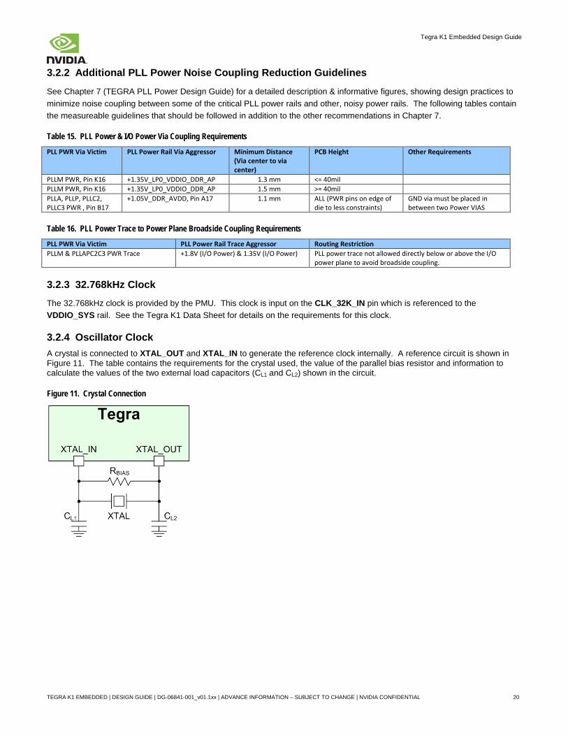
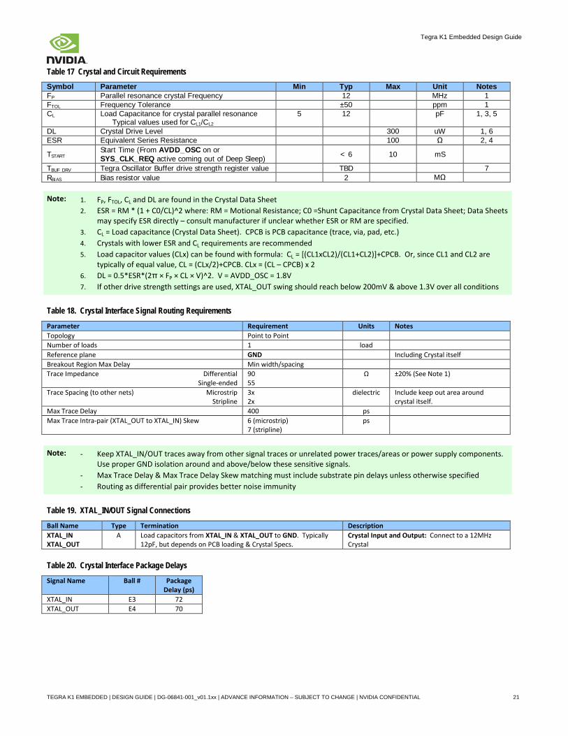
3.2.4 Oscillator Clock A crystal is connected to XTAL_OUT and XTAL_IN to generate the reference clock internally. A reference circuit is shown in Figure 11. The table contains the requirements for the crystal used, the value of the parallel bias resistor and information to calculate the values of the two external load capacitors (CL1 and CL2) shown in the circuit.
Figure 11. Crystal Connection
TEGRA K1 EMBEDDED | DESIGN GUIDE | DG-06841-001_v01.1xx | ADVANCE INFORMATION – SUBJECT TO CHANGE | NVIDIA CONFIDENTIAL 20
Tegra K1 Embedded Design Guide
Table 17 Crystal and Circuit Requirements Symbol Parameter Min Typ Max Unit Notes FP Parallel resonance crystal Frequency 12 MHz 1 FTOL Frequency Tolerance ±50 ppm 1 CL Load Capacitance for crystal parallel resonance
TSTART Start Time (From AVDD_OSC on or SYS_CLK_REQ active coming out of Deep Sleep) < 6 10 mS
TBUF_DRV Tegra Oscillator Buffer drive strength register value TBD 7 RBIAS Bias resistor value 2 MΩ Note: 1. FP, FTOL, CL and DL are found in the Crystal Data Sheet
2. ESR = RM * (1 + C0/CL)^2 where: RM = Motional Resistance; C0 =Shunt Capacitance from Crystal Data Sheet; Data Sheets may specify ESR directly – consult manufacturer if unclear whether ESR or RM are specified.
3. CL = Load capacitance (Crystal Data Sheet). CPCB is PCB capacitance (trace, via, pad, etc.) 4. Crystals with lower ESR and CL requirements are recommended 5. Load capacitor values (CLx) can be found with formula: CL = [(CL1xCL2)/(CL1+CL2)]+CPCB. Or, since CL1 and CL2 are
typically of equal value, CL = (CLx/2)+CPCB. CLx = (CL – CPCB) x 2 6. DL = 0.5*ESR*(2π × FP × CL × V)^2. V = AVDD_OSC = 1.8V 7. If other drive strength settings are used, XTAL_OUT swing should reach below 200mV & above 1.3V over all conditions
Table 18. Crystal Interface Signal Routing Requirements
Parameter Requirement Units Notes Topology Point to Point Number of loads 1 load Reference plane GND Including Crystal itself Breakout Region Max Delay Min width/spacing Trace Impedance Differential Single-ended
90 55
Ω ±20% (See Note 1)
Trace Spacing (to other nets) Microstrip Stripline
3x 2x
dielectric Include keep out area around crystal itself.
Max Trace Delay 400 ps Max Trace Intra-pair (XTAL_OUT to XTAL_IN) Skew 6 (microstrip)
7 (stripline) ps
Note: - Keep XTAL_IN/OUT traces away from other signal traces or unrelated power traces/areas or power supply components.
Use proper GND isolation around and above/below these sensitive signals. - Max Trace Delay & Max Trace Delay Skew matching must include substrate pin delays unless otherwise specified - Routing as differential pair provides better noise immunity
Table 19. XTAL_IN/OUT Signal Connections
Ball Name Type Termination Description XTAL_IN XTAL_OUT
A Load capacitors from XTAL_IN & XTAL_OUT to GND. Typically 12pF, but depends on PCB loading & Crystal Specs.
Crystal Input and Output: Connect to a 12MHz Crystal
Table 20. Crystal Interface Package Delays
Signal Name Ball # Package Delay (ps)
XTAL_IN E3 72 XTAL_OUT E4 70
TEGRA K1 EMBEDDED | DESIGN GUIDE | DG-06841-001_v01.1xx | ADVANCE INFORMATION – SUBJECT TO CHANGE | NVIDIA CONFIDENTIAL 21
Tegra K1 Embedded Design Guide
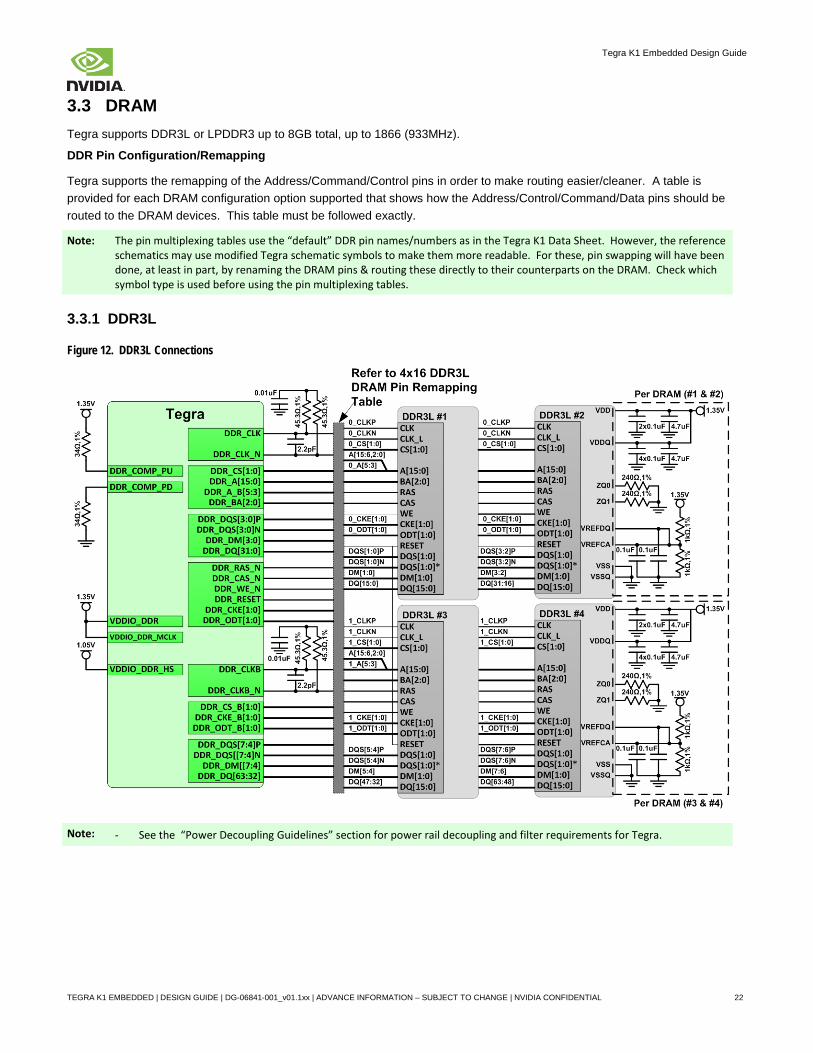
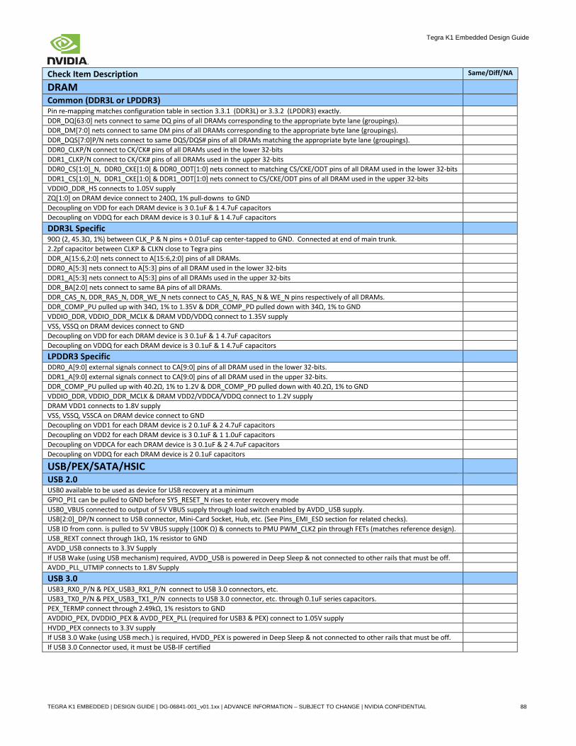
3.3 DRAM Tegra supports DDR3L or LPDDR3 up to 8GB total, up to 1866 (933MHz).
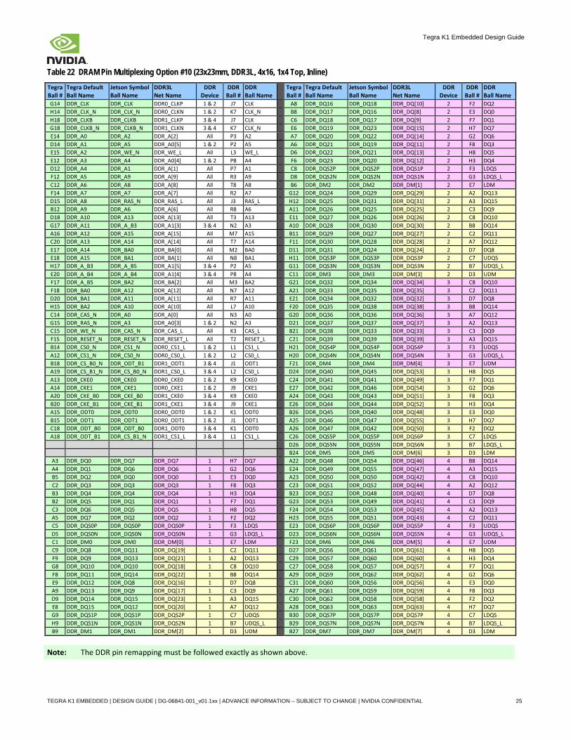
DDR Pin Configuration/Remapping
Tegra supports the remapping of the Address/Command/Control pins in order to make routing easier/cleaner. A table is provided for each DRAM configuration option supported that shows how the Address/Control/Command/Data pins should be routed to the DRAM devices. This table must be followed exactly.
Note: The pin multiplexing tables use the “default” DDR pin names/numbers as in the Tegra K1 Data Sheet. However, the reference schematics may use modified Tegra schematic symbols to make them more readable. For these, pin swapping will have been done, at least in part, by renaming the DRAM pins & routing these directly to their counterparts on the DRAM. Check which symbol type is used before using the pin multiplexing tables.
3.3.1 DDR3L
Figure 12. DDR3L Connections
Note: - See the “Power Decoupling Guidelines” section for power rail decoupling and filter requirements for Tegra.
TEGRA K1 EMBEDDED | DESIGN GUIDE | DG-06841-001_v01.1xx | ADVANCE INFORMATION – SUBJECT TO CHANGE | NVIDIA CONFIDENTIAL 22
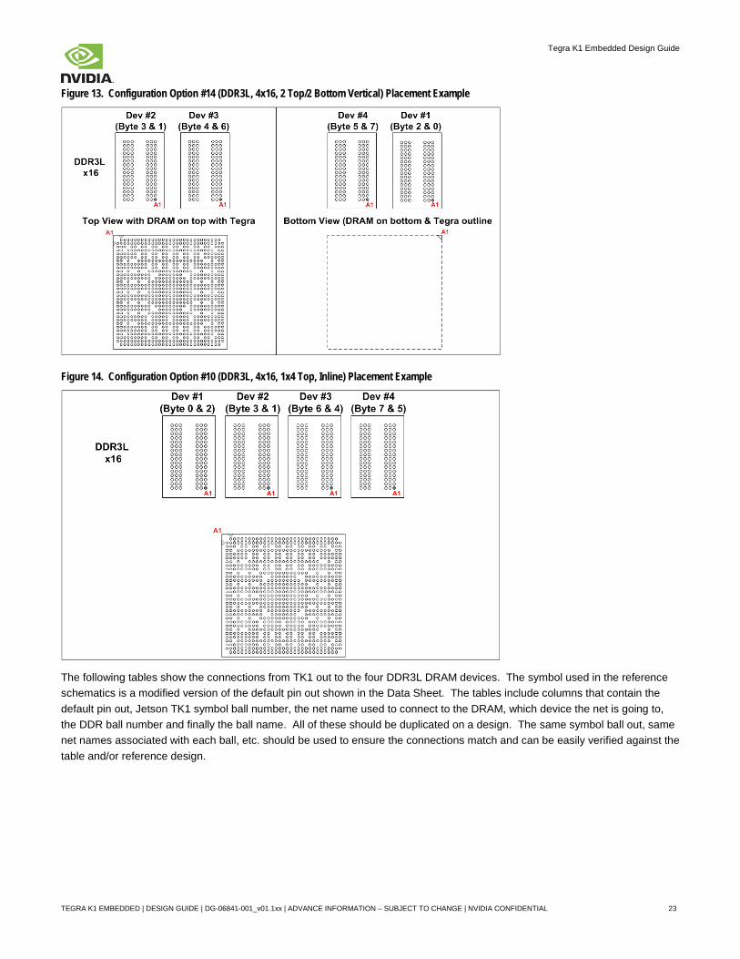
The following tables show the connections from TK1 out to the four DDR3L DRAM devices. The symbol used in the reference schematics is a modified version of the default pin out shown in the Data Sheet. The tables include columns that contain the default pin out, Jetson TK1 symbol ball number, the net name used to connect to the DRAM, which device the net is going to, the DDR ball number and finally the ball name. All of these should be duplicated on a design. The same symbol ball out, same net names associated with each ball, etc. should be used to ensure the connections match and can be easily verified against the table and/or reference design.
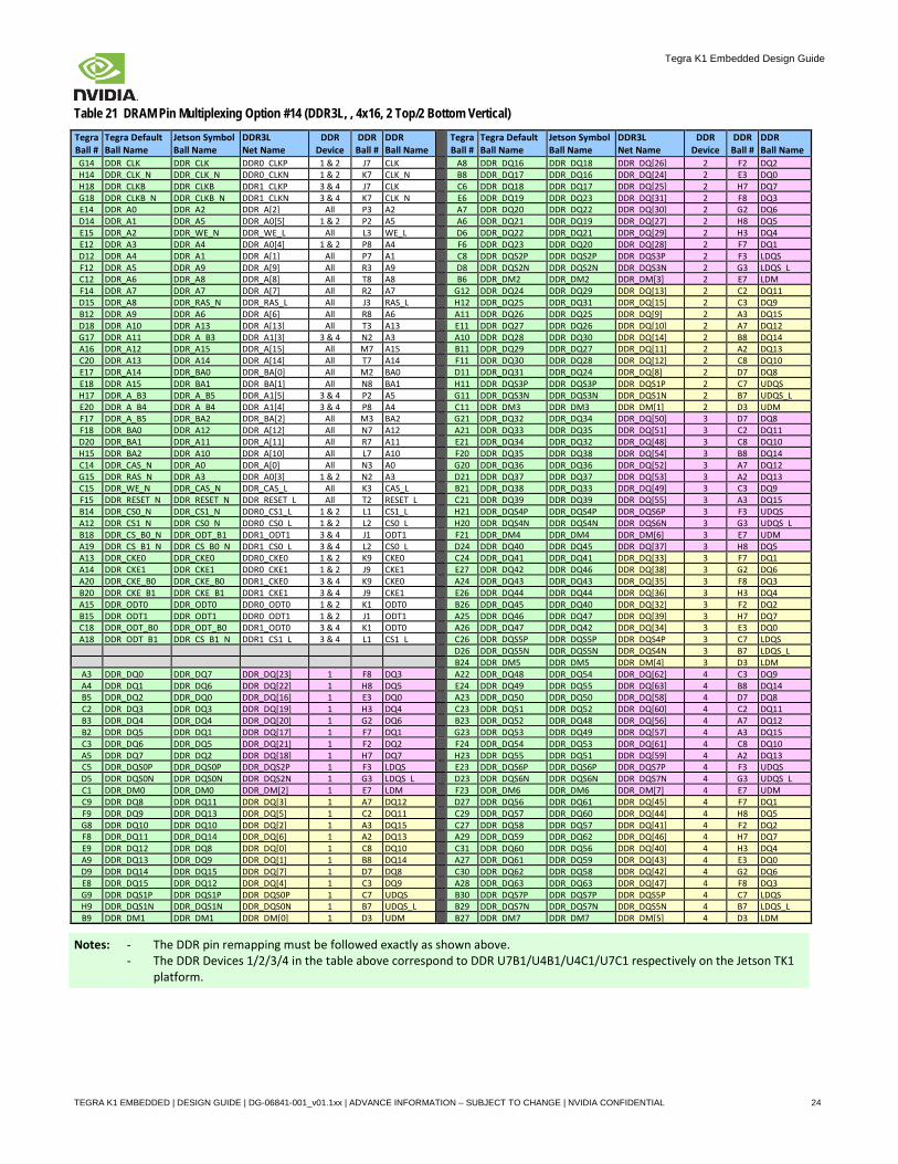
TEGRA K1 EMBEDDED | DESIGN GUIDE | DG-06841-001_v01.1xx | ADVANCE INFORMATION – SUBJECT TO CHANGE | NVIDIA CONFIDENTIAL 23
Notes: - The DDR pin remapping must be followed exactly as shown above. - The DDR Devices 1/2/3/4 in the table above correspond to DDR U7B1/U4B1/U4C1/U7C1 respectively on the Jetson TK1
platform.
TEGRA K1 EMBEDDED | DESIGN GUIDE | DG-06841-001_v01.1xx | ADVANCE INFORMATION – SUBJECT TO CHANGE | NVIDIA CONFIDENTIAL 24
Note: The DDR pin remapping must be followed exactly as shown above.
TEGRA K1 EMBEDDED | DESIGN GUIDE | DG-06841-001_v01.1xx | ADVANCE INFORMATION – SUBJECT TO CHANGE | NVIDIA CONFIDENTIAL 25
Tegra K1 Embedded Design Guide
DDR3L Design Guidelines
Notes: - The topology for each signal must be followed exactly as shown in the figures included for each signal group. The Requirements are 32-bit channel except the DDR0_CLKP/DDR0_CLKN to DDR1_CLKP/DDR1_CLKN requirement.
- New Skew requirement term definitions: o “Center, +/-“ mean the skew is measured from the clock/strobe (center signal) to the related signals, either before
or after the strobe/clock and must meet the required max value. o “Absolute” mean the maximum skew between any of the signals listed is within the required max value. o “Load to Load” means that the skew is the total of the path from Tegra out to the destination (load) for each signal
involved in the requirement. This allows for asymmetric routing of the different branches in T-topologies, as long as the total lengths/delays are within the requirement value.
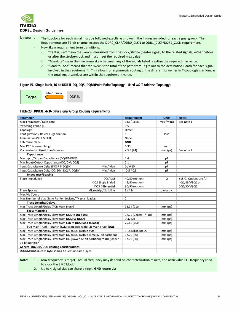
Figure 15. Single Rank, 16-bit DDR3L DQ, DQS, DQM (Point-Point Topology – Used w/2-T Address Topology)
Table 23. DDR3L, 4x16 Data Signal Group Routing Requirements
Parameter Requirement Units Notes Max Frequency / Data Rate 933 / 1866 MHz/Mbps See note 1 Switching Period (T) 0.5 T Topology Direct Configuration / Device Organization 1 load Termination (VTT & ODT) None Reference plane GND Max PCB breakout length 6.35 mm Via proximity (Signal to reference) < 3.8 (24) mm (ps) See note 2 Capacitance Min Input/Output Capacitance (DQ/DM/DQS) 1.4 pF Max Input/Output Capacitance (DQ/DM/DQS) 2.1 pF Input Capacitance Delta (DQSP & DQSN) Min / Max 0 / 0.15 pF Input Capacitance Delta(DQ, DM, DQSP, DQSN) Min / Max -0.5 / 0.3 pF Impedance/Spacing Trace Impedance DQ / DM DQS Single Ended DQS Differential
40/50 (option) 45/50 (option) 80/90 (option)
Ω ±15%. Options are for 40Ω/45Ω/80Ω or 50Ω/50Ω/90Ω
Trace Spacing Microstrip / Stripline 3x / 2x dielectric Max Via Count Max Number of Vias (Tx to Rx (Per device) / Tx to all loads): 2 Trace Lengths/Delays Max Trace Length/Delay (PCB Main Trunk) 33.34 (210) mm (ps) Skew Matching Max Trace Length/Delay Skew from DQS to DQ / DM 1.575 (Center +/- 10) mm (ps) Max Trace Length/Delay Skew from DQSP & DQSN 0.32 (2) mm (ps) Max Trace Length/Delay Skew from CLK to DQS (load to load)
PCB Main Trunk + Branch (CLK) compared withPCB Main Trunk (DQS) 25.40 (160) mm (ps)
Max Trace Length/Delay Skew from DQ to DQ (within byte) 3.18 (Absolute 20) mm (ps) Max Trace Length/Delay Skew from DQ to DQ (within same 32-bit partition) 12.70 (80) mm (ps) Max Trace Length/Delay Skew from DQ (Lower 32-bit partition) to DQ (Upper 32-bit partition)
12.70 (80) mm (ps)
General DQ/DM/DQS Routing Considerations DQ/DM/DQS in each byte should be kept on same layer
Note: 1. Max frequency is target. Actual frequency may depend on characterization results, and achievable PLL frequency used to clock the EMC block
2. Up to 4 signal vias can share a single GND return via
TEGRA K1 EMBEDDED | DESIGN GUIDE | DG-06841-001_v01.1xx | ADVANCE INFORMATION – SUBJECT TO CHANGE | NVIDIA CONFIDENTIAL 26
Tegra K1 Embedded Design Guide
Table 24. DDR3L, 4x16 Data Signal Group Connections
Signal Name Type Termination Description DDR_DQ[63:0] DDR_DM[7:0] DDR_DQS[7:0]P/N
I/O O
DIFF I/O
No VTT or ODT (On-Die Termination) Required
Data: Connect to DQ pins of all DRAMs (see table below) Data Mask: Connect to DM pins on DRAMs (see table below) Data Strobes: Connect to DQSxP/DQSxN pins of all DRAM (table below) Byte Lanes (Groupings) per channel Data Data Mask Data Strobe Data Data Mask Data Strobe DQ[7:0] DM0 DQS0P/N DQ[39:32] DM4 DQS4P/N DQ[15:8] DM1 DQS1P/N DQ[47:40] DM5 DQS5P/N DQ[23:16] DM2 DQS2P/N DQ[55:48] DM6 DQS6P/N DQ[31:24] DM3 DQS3P/N DQ[63:56] DM7 DQS7P/N
Note: The Tegra DRAM ball names may not correspond to the signal brought out on that ball. Use the DRAM Pin Multiplexing table
to select the correct Tegra ball to connect to each DDR3L ball.
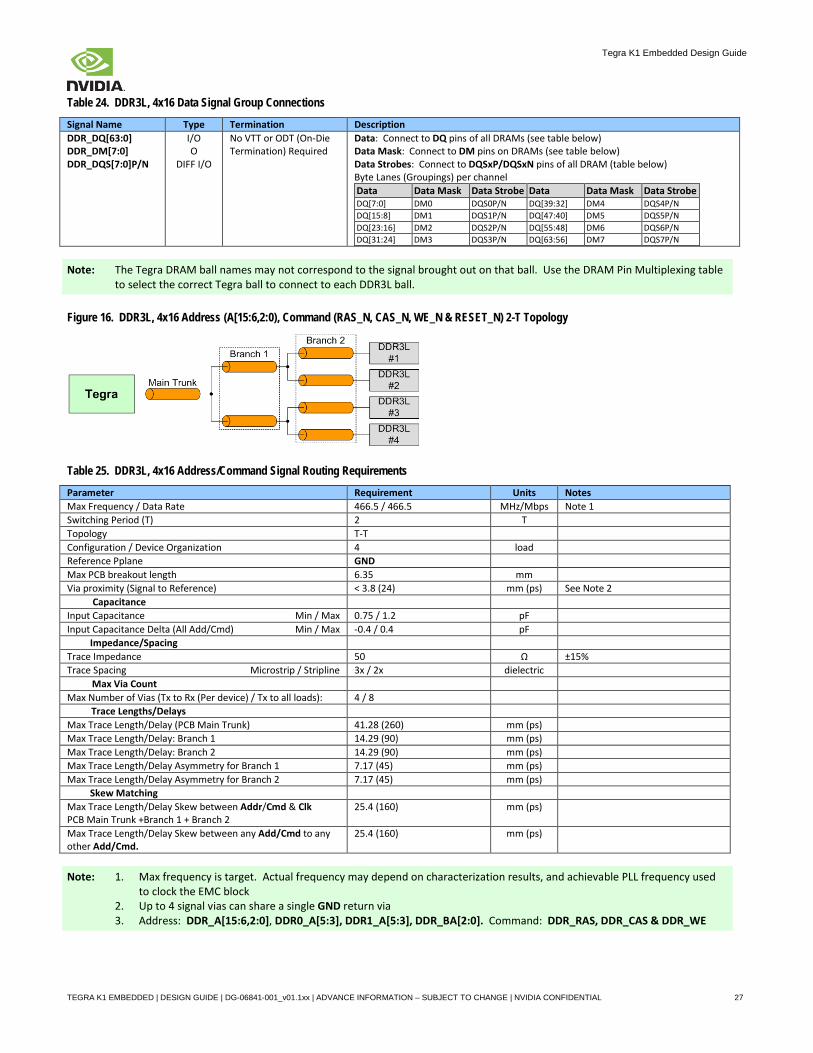
Table 25. DDR3L, 4x16 Address/Command Signal Routing Requirements
Parameter Requirement Units Notes Max Frequency / Data Rate 466.5 / 466.5 MHz/Mbps Note 1 Switching Period (T) 2 T Topology T-T Configuration / Device Organization 4 load Reference Pplane GND Max PCB breakout length 6.35 mm Via proximity (Signal to Reference) < 3.8 (24) mm (ps) See Note 2 Capacitance Input Capacitance Min / Max 0.75 / 1.2 pF Input Capacitance Delta (All Add/Cmd) Min / Max -0.4 / 0.4 pF Impedance/Spacing Trace Impedance 50 Ω ±15% Trace Spacing Microstrip / Stripline 3x / 2x dielectric Max Via Count Max Number of Vias (Tx to Rx (Per device) / Tx to all loads): 4 / 8 Trace Lengths/Delays Max Trace Length/Delay (PCB Main Trunk) 41.28 (260) mm (ps) Max Trace Length/Delay: Branch 1 14.29 (90) mm (ps) Max Trace Length/Delay: Branch 2 14.29 (90) mm (ps) Max Trace Length/Delay Asymmetry for Branch 1 7.17 (45) mm (ps) Max Trace Length/Delay Asymmetry for Branch 2 7.17 (45) mm (ps) Skew Matching Max Trace Length/Delay Skew between Addr/Cmd & Clk PCB Main Trunk +Branch 1 + Branch 2
25.4 (160) mm (ps)
Max Trace Length/Delay Skew between any Add/Cmd to any other Add/Cmd.
25.4 (160) mm (ps)
Note: 1. Max frequency is target. Actual frequency may depend on characterization results, and achievable PLL frequency used to clock the EMC block
2. Up to 4 signal vias can share a single GND return via 3. Address: DDR_A[15:6,2:0], DDR0_A[5:3], DDR1_A[5:3], DDR_BA[2:0]. Command: DDR_RAS, DDR_CAS & DDR_WE
TEGRA K1 EMBEDDED | DESIGN GUIDE | DG-06841-001_v01.1xx | ADVANCE INFORMATION – SUBJECT TO CHANGE | NVIDIA CONFIDENTIAL 27
Tegra K1 Embedded Design Guide
Table 26. DDR3L, 4x16 Address/Command Signal Group Connections
Signal Name Type Termination Description DDR_A[15:6,2:0] O Address 15:6, 2:0: Connect to matching Ax pins of all DRAM DDR_BA[2:0] O Bank Address: Connect to BAx pins of all DRAMs DDR_CAS O Column Add. Strobe: Connect to CAS pins of all DRAMs DDR_RAS O Row Address Strobe: Connect to RAS pin of all DRAMs DDR_WE O Write Enable: Connect to WE pin of all DRAMs DDR_RESET_N O Reset: Connect to RESET pin of all DRAMs Note: The Tegra DRAM ball names may not correspond to the signal brought out on that ball. Use the DRAM Pin Multiplexing table
to select the correct Tegra ball to connect to each DDR3L ball.
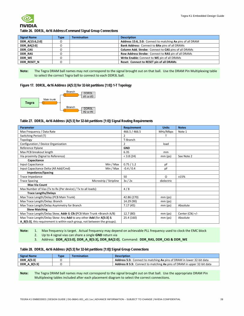
Table 27. DDR3L, 4x16 Address (A[5:3] for 32-bit partitions [1:0]) Signal Routing Requirements
Parameter Requirement Units Notes Max Frequency / Data Rate 466.5 / 466.5 MHz/Mbps Note 1 Switching Period (T) 2 T Topology T-Branch Configuration / Device Organization 2 load Reference Pplane GND Max PCB breakout length 6.35 mm Via proximity (Signal to Reference) < 3.8 (24) mm (ps) See Note 2 Capacitance Input Capacitance Min / Max 0.75 / 1.2 pF Input Capacitance Delta (All Add/Cmd) Min / Max -0.4 / 0.4 pF Impedance/Spacing Trace Impedance 50 Ω ±15% Trace Spacing Microstrip / Stripline 3x / 2x dielectric Max Via Count Max Number of Vias (Tx to Rx (Per device) / Tx to all loads): 4 / 8 Trace Lengths/Delays Max Trace Length/Delay (PCB Main Trunk) 42.86 (270) mm (ps) Max Trace Length/Delay: Branch 14.29 (90) mm (ps) Max Trace Length/Delay Asymmetry for Branch 7.17 (45) mm (ps) Absolute Skew Matching Max Trace Length/Delay Skew, Addr & Clk (PCB Main Trunk +Branch A/B) 12.7 (80) mm (ps) Center (Clk) +/- Max Trace Length/Delay Skew: Any Add to any other Add (for A[5:3] & A_B[5:3], this requirement is within each group, not between the groups).
25.4 (160) mm (ps) Absolute
Note: 1. Max frequency is target. Actual frequency may depend on achievable PLL frequency used to clock the EMC block 2. Up to 4 signal vias can share a single GND return via 3. Address: DDR_A[15:0], DDR_A_B[5:3], DDR_BA[2:0]. Command: DDR_RAS, DDR_CAS & DDR_WE
Table 28. DDR3L, 4x16 Address (A[5:3] for 32-bit partitions [1:0]) Signal Group Connections
Signal Name Type Termination Description DDR_A[5:3] O Address 5:3: Connect to matching Ax pins of DRAM in lower 32-bit data DDR_A_B[5:3] O Address B 5:3: Connect to matching Ax pins of DRAM in upper 32-bit data Note: The Tegra DRAM ball names may not correspond to the signal brought out on that ball. Use the appropriate DRAM Pin
Multiplexing tables included after each placement diagram to select the correct connections.
TEGRA K1 EMBEDDED | DESIGN GUIDE | DG-06841-001_v01.1xx | ADVANCE INFORMATION – SUBJECT TO CHANGE | NVIDIA CONFIDENTIAL 28
Tegra K1 Embedded Design Guide
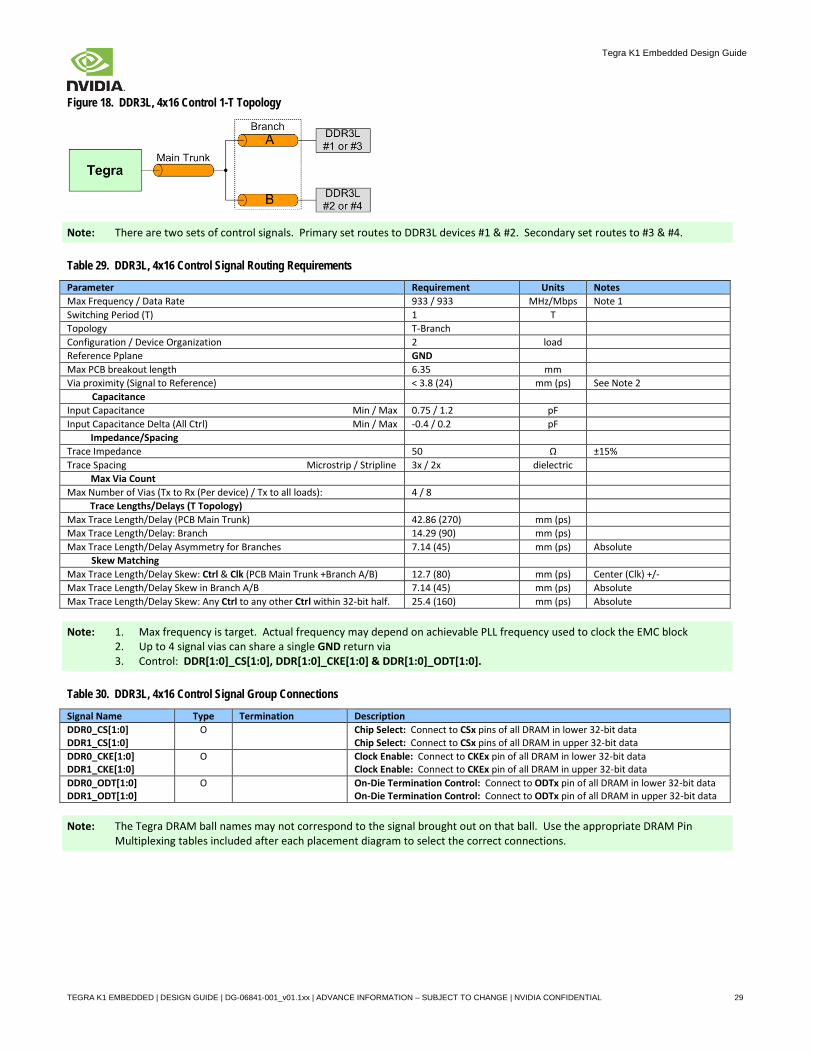
Figure 18. DDR3L, 4x16 Control 1-T Topology
Note: There are two sets of control signals. Primary set routes to DDR3L devices #1 & #2. Secondary set routes to #3 & #4.
Table 29. DDR3L, 4x16 Control Signal Routing Requirements
Parameter Requirement Units Notes Max Frequency / Data Rate 933 / 933 MHz/Mbps Note 1 Switching Period (T) 1 T Topology T-Branch Configuration / Device Organization 2 load Reference Pplane GND Max PCB breakout length 6.35 mm Via proximity (Signal to Reference) < 3.8 (24) mm (ps) See Note 2 Capacitance Input Capacitance Min / Max 0.75 / 1.2 pF Input Capacitance Delta (All Ctrl) Min / Max -0.4 / 0.2 pF Impedance/Spacing Trace Impedance 50 Ω ±15% Trace Spacing Microstrip / Stripline 3x / 2x dielectric Max Via Count Max Number of Vias (Tx to Rx (Per device) / Tx to all loads): 4 / 8 Trace Lengths/Delays (T Topology) Max Trace Length/Delay (PCB Main Trunk) 42.86 (270) mm (ps) Max Trace Length/Delay: Branch 14.29 (90) mm (ps) Max Trace Length/Delay Asymmetry for Branches 7.14 (45) mm (ps) Absolute Skew Matching Max Trace Length/Delay Skew: Ctrl & Clk (PCB Main Trunk +Branch A/B) 12.7 (80) mm (ps) Center (Clk) +/- Max Trace Length/Delay Skew in Branch A/B 7.14 (45) mm (ps) Absolute Max Trace Length/Delay Skew: Any Ctrl to any other Ctrl within 32-bit half. 25.4 (160) mm (ps) Absolute
Note: 1. Max frequency is target. Actual frequency may depend on achievable PLL frequency used to clock the EMC block 2. Up to 4 signal vias can share a single GND return via 3. Control: DDR[1:0]_CS[1:0], DDR[1:0]_CKE[1:0] & DDR[1:0]_ODT[1:0].
Table 30. DDR3L, 4x16 Control Signal Group Connections
Signal Name Type Termination Description DDR0_CS[1:0] DDR1_CS[1:0]
O Chip Select: Connect to CSx pins of all DRAM in lower 32-bit data Chip Select: Connect to CSx pins of all DRAM in upper 32-bit data
DDR0_CKE[1:0] DDR1_CKE[1:0]
O Clock Enable: Connect to CKEx pin of all DRAM in lower 32-bit data Clock Enable: Connect to CKEx pin of all DRAM in upper 32-bit data
DDR0_ODT[1:0] DDR1_ODT[1:0]
O On-Die Termination Control: Connect to ODTx pin of all DRAM in lower 32-bit data On-Die Termination Control: Connect to ODTx pin of all DRAM in upper 32-bit data
Note: The Tegra DRAM ball names may not correspond to the signal brought out on that ball. Use the appropriate DRAM Pin
Multiplexing tables included after each placement diagram to select the correct connections.
TEGRA K1 EMBEDDED | DESIGN GUIDE | DG-06841-001_v01.1xx | ADVANCE INFORMATION – SUBJECT TO CHANGE | NVIDIA CONFIDENTIAL 29
Tegra K1 Embedded Design Guide
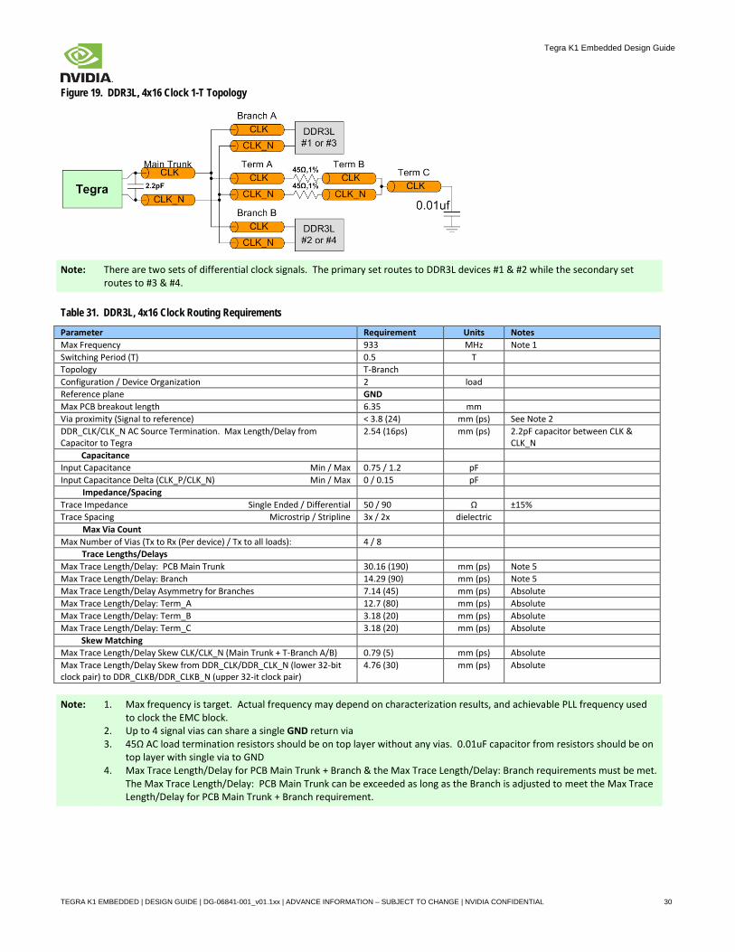
Figure 19. DDR3L, 4x16 Clock 1-T Topology
Note: There are two sets of differential clock signals. The primary set routes to DDR3L devices #1 & #2 while the secondary set routes to #3 & #4.
Table 31. DDR3L, 4x16 Clock Routing Requirements
Parameter Requirement Units Notes Max Frequency 933 MHz Note 1 Switching Period (T) 0.5 T Topology T-Branch Configuration / Device Organization 2 load Reference plane GND Max PCB breakout length 6.35 mm Via proximity (Signal to reference) < 3.8 (24) mm (ps) See Note 2 DDR_CLK/CLK_N AC Source Termination. Max Length/Delay from Capacitor to Tegra
2.54 (16ps) mm (ps) 2.2pF capacitor between CLK & CLK_N
Capacitance Input Capacitance Min / Max 0.75 / 1.2 pF Input Capacitance Delta (CLK_P/CLK_N) Min / Max 0 / 0.15 pF Impedance/Spacing Trace Impedance Single Ended / Differential 50 / 90 Ω ±15% Trace Spacing Microstrip / Stripline 3x / 2x dielectric Max Via Count Max Number of Vias (Tx to Rx (Per device) / Tx to all loads): 4 / 8 Trace Lengths/Delays Max Trace Length/Delay: PCB Main Trunk 30.16 (190) mm (ps) Note 5 Max Trace Length/Delay: Branch 14.29 (90) mm (ps) Note 5 Max Trace Length/Delay Asymmetry for Branches 7.14 (45) mm (ps) Absolute Max Trace Length/Delay: Term_A 12.7 (80) mm (ps) Absolute Max Trace Length/Delay: Term_B 3.18 (20) mm (ps) Absolute Max Trace Length/Delay: Term_C 3.18 (20) mm (ps) Absolute Skew Matching Max Trace Length/Delay Skew CLK/CLK_N (Main Trunk + T-Branch A/B) 0.79 (5) mm (ps) Absolute Max Trace Length/Delay Skew from DDR_CLK/DDR_CLK_N (lower 32-bit clock pair) to DDR_CLKB/DDR_CLKB_N (upper 32-it clock pair)
4.76 (30) mm (ps) Absolute
Note: 1. Max frequency is target. Actual frequency may depend on characterization results, and achievable PLL frequency used to clock the EMC block.
2. Up to 4 signal vias can share a single GND return via 3. 45Ω AC load termination resistors should be on top layer without any vias. 0.01uF capacitor from resistors should be on
top layer with single via to GND 4. Max Trace Length/Delay for PCB Main Trunk + Branch & the Max Trace Length/Delay: Branch requirements must be met.
The Max Trace Length/Delay: PCB Main Trunk can be exceeded as long as the Branch is adjusted to meet the Max Trace Length/Delay for PCB Main Trunk + Branch requirement.
TEGRA K1 EMBEDDED | DESIGN GUIDE | DG-06841-001_v01.1xx | ADVANCE INFORMATION – SUBJECT TO CHANGE | NVIDIA CONFIDENTIAL 30
Tegra K1 Embedded Design Guide
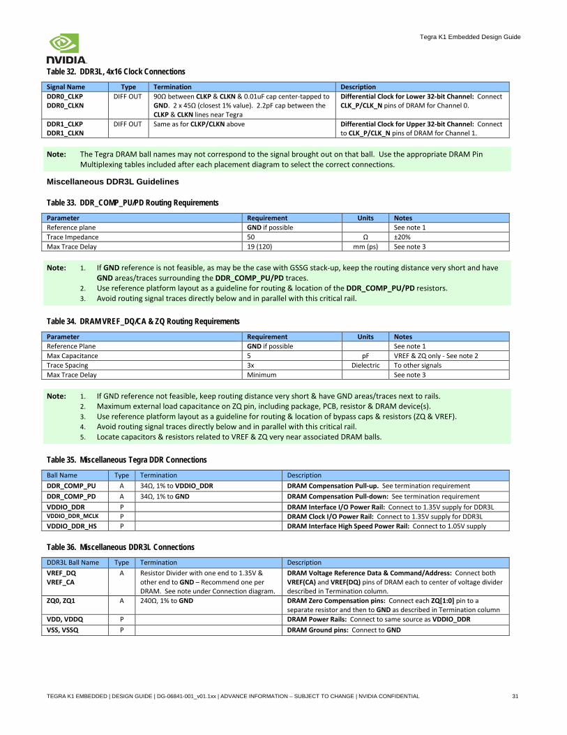
Table 32. DDR3L, 4x16 Clock Connections
Signal Name Type Termination Description DDR0_CLKP DDR0_CLKN
DIFF OUT 90Ω between CLKP & CLKN & 0.01uF cap center-tapped to GND. 2 x 45Ω (closest 1% value). 2.2pF cap between the CLKP & CLKN lines near Tegra
Differential Clock for Lower 32-bit Channel: Connect CLK_P/CLK_N pins of DRAM for Channel 0.
DDR1_CLKP DDR1_CLKN
DIFF OUT Same as for CLKP/CLKN above Differential Clock for Upper 32-bit Channel: Connect to CLK_P/CLK_N pins of DRAM for Channel 1.
Note: The Tegra DRAM ball names may not correspond to the signal brought out on that ball. Use the appropriate DRAM Pin
Multiplexing tables included after each placement diagram to select the correct connections.
Miscellaneous DDR3L Guidelines
Table 33. DDR_COMP_PU/PD Routing Requirements
Parameter Requirement Units Notes Reference plane GND if possible See note 1 Trace Impedance 50 Ω ±20% Max Trace Delay 19 (120) mm (ps) See note 3
Note: 1. If GND reference is not feasible, as may be the case with GSSG stack-up, keep the routing distance very short and have GND areas/traces surrounding the DDR_COMP_PU/PD traces.
2. Use reference platform layout as a guideline for routing & location of the DDR_COMP_PU/PD resistors. 3. Avoid routing signal traces directly below and in parallel with this critical rail.
Table 34. DRAM VREF_DQ/CA & ZQ Routing Requirements
Parameter Requirement Units Notes Reference Plane GND if possible See note 1 Max Capacitance 5 pF VREF & ZQ only - See note 2 Trace Spacing 3x Dielectric To other signals Max Trace Delay Minimum See note 3
Note: 1. If GND reference not feasible, keep routing distance very short & have GND areas/traces next to rails. 2. Maximum external load capacitance on ZQ pin, including package, PCB, resistor & DRAM device(s). 3. Use reference platform layout as a guideline for routing & location of bypass caps & resistors (ZQ & VREF). 4. Avoid routing signal traces directly below and in parallel with this critical rail. 5. Locate capacitors & resistors related to VREF & ZQ very near associated DRAM balls.
Table 35. Miscellaneous Tegra DDR Connections
Ball Name Type Termination Description DDR_COMP_PU A 34Ω, 1% to VDDIO_DDR DRAM Compensation Pull-up. See termination requirement DDR_COMP_PD A 34Ω, 1% to GND DRAM Compensation Pull-down: See termination requirement VDDIO_DDR P DRAM Interface I/O Power Rail: Connect to 1.35V supply for DDR3L VDDIO_DDR_MCLK P DRAM Clock I/O Power Rail: Connect to 1.35V supply for DDR3L VDDIO_DDR_HS P DRAM Interface High Speed Power Rail: Connect to 1.05V supply
Table 36. Miscellaneous DDR3L Connections
DDR3L Ball Name Type Termination Description VREF_DQ VREF_CA
A Resistor Divider with one end to 1.35V & other end to GND – Recommend one per DRAM. See note under Connection diagram.
DRAM Voltage Reference Data & Command/Address: Connect both VREF(CA) and VREF(DQ) pins of DRAM each to center of voltage divider described in Termination column.
ZQ0, ZQ1 A 240Ω, 1% to GND DRAM Zero Compensation pins: Connect each ZQ[1:0] pin to a separate resistor and then to GND as described in Termination column
VDD, VDDQ P DRAM Power Rails: Connect to same source as VDDIO_DDR VSS, VSSQ P DRAM Ground pins: Connect to GND
TEGRA K1 EMBEDDED | DESIGN GUIDE | DG-06841-001_v01.1xx | ADVANCE INFORMATION – SUBJECT TO CHANGE | NVIDIA CONFIDENTIAL 31
Tegra K1 Embedded Design Guide
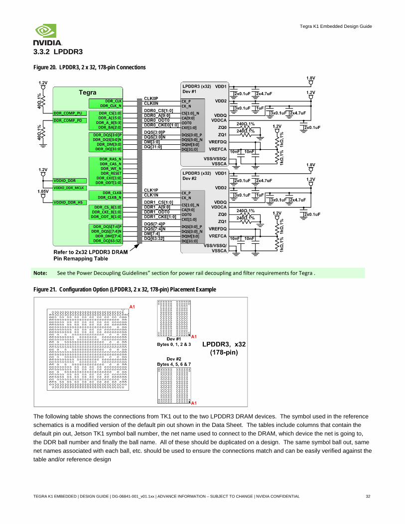
3.3.2 LPDDR3
Figure 20. LPDDR3, 2 x 32, 178-pin Connections
Note: See the Power Decoupling Guidelines” section for power rail decoupling and filter requirements for Tegra .
Figure 21. Configuration Option (LPDDR3, 2 x 32, 178-pin) Placement Example
The following table shows the connections from TK1 out to the two LPDDR3 DRAM devices. The symbol used in the reference schematics is a modified version of the default pin out shown in the Data Sheet. The tables include columns that contain the default pin out, Jetson TK1 symbol ball number, the net name used to connect to the DRAM, which device the net is going to, the DDR ball number and finally the ball name. All of these should be duplicated on a design. The same symbol ball out, same net names associated with each ball, etc. should be used to ensure the connections match and can be easily verified against the table and/or reference design
TEGRA K1 EMBEDDED | DESIGN GUIDE | DG-06841-001_v01.1xx | ADVANCE INFORMATION – SUBJECT TO CHANGE | NVIDIA CONFIDENTIAL 32
Tegra K1 Embedded Design Guide
Table 37 DRAM Pin Multiplexing Option (LPDDR3, 2 x 32, 178-pin) Tegra Ball #
Note: The DDR pin remapping must be followed exactly as shown above.
TEGRA K1 EMBEDDED | DESIGN GUIDE | DG-06841-001_v01.1xx | ADVANCE INFORMATION – SUBJECT TO CHANGE | NVIDIA CONFIDENTIAL 33
Tegra K1 Embedded Design Guide
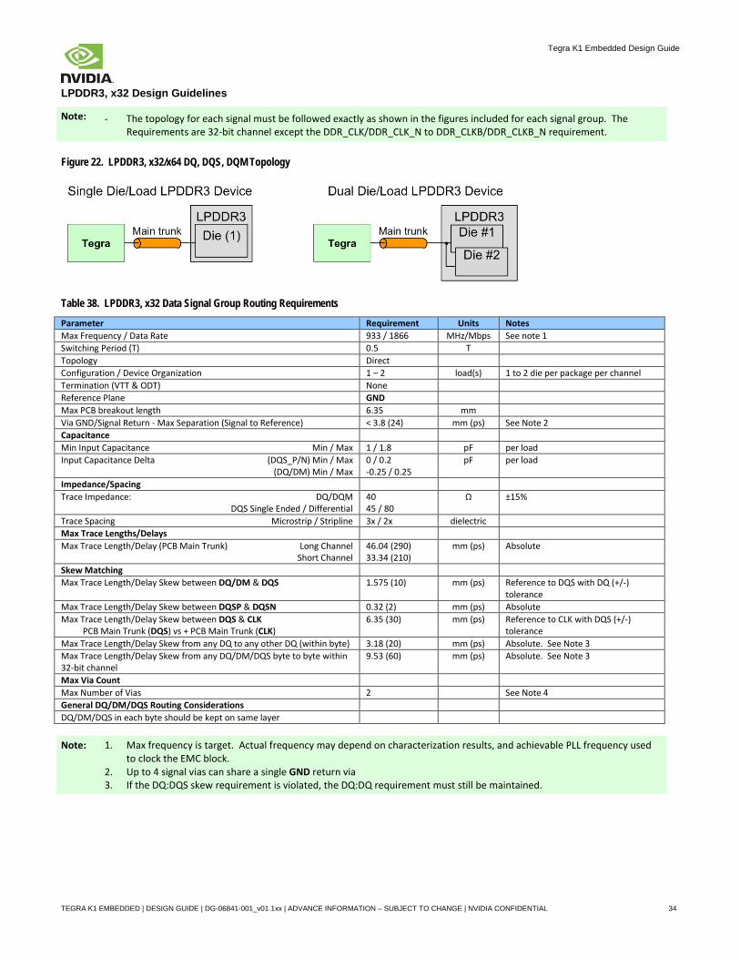
LPDDR3, x32 Design Guidelines
Note: - The topology for each signal must be followed exactly as shown in the figures included for each signal group. The Requirements are 32-bit channel except the DDR_CLK/DDR_CLK_N to DDR_CLKB/DDR_CLKB_N requirement.
Figure 22. LPDDR3, x32/x64 DQ, DQS, DQM Topology
Table 38. LPDDR3, x32 Data Signal Group Routing Requirements
Parameter Requirement Units Notes Max Frequency / Data Rate 933 / 1866 MHz/Mbps See note 1 Switching Period (T) 0.5 T Topology Direct Configuration / Device Organization 1 – 2 load(s) 1 to 2 die per package per channel Termination (VTT & ODT) None Reference Plane GND Max PCB breakout length 6.35 mm Via GND/Signal Return - Max Separation (Signal to Reference) < 3.8 (24) mm (ps) See Note 2 Capacitance Min Input Capacitance Min / Max 1 / 1.8 pF per load Input Capacitance Delta (DQS_P/N) Min / Max (DQ/DM) Min / Max
0 / 0.2 -0.25 / 0.25
pF per load
Impedance/Spacing Trace Impedance: DQ/DQM DQS Single Ended / Differential
40 45 / 80
Ω ±15%
Trace Spacing Microstrip / Stripline 3x / 2x dielectric Max Trace Lengths/Delays Max Trace Length/Delay (PCB Main Trunk) Long Channel Short Channel
46.04 (290) 33.34 (210)
mm (ps) Absolute
Skew Matching Max Trace Length/Delay Skew between DQ/DM & DQS 1.575 (10) mm (ps) Reference to DQS with DQ (+/-)
tolerance Max Trace Length/Delay Skew between DQSP & DQSN 0.32 (2) mm (ps) Absolute Max Trace Length/Delay Skew between DQS & CLK
PCB Main Trunk (DQS) vs + PCB Main Trunk (CLK) 6.35 (30) mm (ps) Reference to CLK with DQS (+/-)
tolerance Max Trace Length/Delay Skew from any DQ to any other DQ (within byte) 3.18 (20) mm (ps) Absolute. See Note 3 Max Trace Length/Delay Skew from any DQ/DM/DQS byte to byte within 32-bit channel
9.53 (60) mm (ps) Absolute. See Note 3
Max Via Count Max Number of Vias 2 See Note 4 General DQ/DM/DQS Routing Considerations DQ/DM/DQS in each byte should be kept on same layer
Note: 1. Max frequency is target. Actual frequency may depend on characterization results, and achievable PLL frequency used to clock the EMC block.
2. Up to 4 signal vias can share a single GND return via 3. If the DQ:DQS skew requirement is violated, the DQ:DQ requirement must still be maintained.
TEGRA K1 EMBEDDED | DESIGN GUIDE | DG-06841-001_v01.1xx | ADVANCE INFORMATION – SUBJECT TO CHANGE | NVIDIA CONFIDENTIAL 34
Tegra K1 Embedded Design Guide
Table 39. LPDDR3, x32 Data Signal Group Connections
Signal Name Type Termination Description DDR_DQ[63:0] DDR_DM[7:0] DDR_DQS[7:0]P/N
I/O O
DIFF I/O
No VTT or ODT (On-Die Termination) Required
Data: Connect to DQ pins of all DRAMs (see table below) Data Mask: Connect to DM pins on DRAMs (see table below) Data Strobes: Connect to DQSxP/DQSxN pins of all DRAM (table below) Byte Lanes (Groupings) per channel Data Data Mask Data Strobe Data Data Mask Data Strobe DQ[7:0] DM0 DQS0P/N DQ[39:32] DM4 DQS4P/N DQ[15:8] DM1 DQS1P/N DQ[47:40] DM5 DQS5P/N DQ[23:16] DM2 DQS2P/N DQ[55:48] DM6 DQS6P/N DQ[31:24] DM3 DQS3P/N DQ[63:56] DM7 DQS7P/N
Note: The Tegra DRAM ball names may not correspond to the signal brought out on that ball. Use the DRAM Pin Multiplexing table
to select the correct Tegra ball to connect to each DRAM ball.
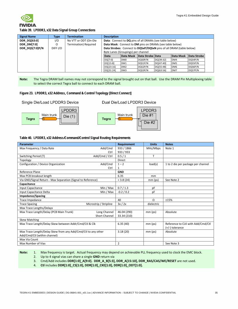
Table 40. LPDDR3, x32 Address/Command/Control Signal Routing Requirements
Parameter Requirement Units Notes Max Frequency / Data Rate Add/Cmd Ctrl
933 / 1866 933 / 933
MHz/Mbps Note 1
Switching Period (T) Add/Cmd / Ctrl 0.5 / 1 T Topology Direct Configuration / Device Organization Add/Cmd Ctrl
1 – 2 1
load(s) 1 to 2 die per package per channel
Reference Plane GND Max PCB breakout length 6.35 mm Via GND/Signal Return - Max Separation (Signal to Reference) < 3.8 (24) mm (ps) See Note 2 Capacitance Input Capacitance Min / Max 0.7 / 1.3 pF Input Capacitance Delta Min / Max -0.2 / 0.2 pF Impedance/Spacing Trace Impedance 40 Ω ±15% Trace Spacing Microstrip / Stripline 3x / 2x dielectric Max Trace Lengths/Delays Max Trace Length/Delay (PCB Main Trunk) Long Channel Short Channel
46.04 (290) 33.34 (210)
mm (ps) Absolute
Skew Matching Max Trace Length/Delay Skew between Addr/Cmd/Ctl & Clk 6.35 (40) mm (ps) Reference to CLK with Add/Cmd/Ctl
(+/-) tolerance Max Trace Length/Delay Skew from any Add/Cmd/Ctl to any other Add/Cmd/Ctl (within channel)
3.18 (20) mm (ps) Absolute
Max Via Count Max Number of Vias 2 See Note 3
Note: 1. Max frequency is target. Actual frequency may depend on achievable PLL frequency used to clock the EMC block. 2. Up to 4 signal vias can share a single GND return via 3. Cmd/Add includes DDR[1:0]_A[9:0]. DDR_A_B[5:3], DDR_A[15:10], DDR_RAS/CAS/WE/RESET are not used. 4. Ctl includes DDR[1:0]_CS[1:0], DDR[1:0]_CKE[1:0], DDR[1:0]_ODT[1:0].
TEGRA K1 EMBEDDED | DESIGN GUIDE | DG-06841-001_v01.1xx | ADVANCE INFORMATION – SUBJECT TO CHANGE | NVIDIA CONFIDENTIAL 35
Tegra K1 Embedded Design Guide
Table 41. LPDDR3, x32 Command/Address & Control Group Connections
Signal Name Type Termination Description DDR0_A[9:0] DDR1_A[9:0]
O Address 9:0: Connect to CA 9:0 pins of lower 32-bit DRAM
Parameter Requirement Units Notes Max Frequency 933 MHz See Note 1 Switching Period (T) 0.5 T Topology Direct Configuration / Device Organization 1 – 2 load(s) 1 to 2 die per package per channel Reference Plane GND Max PCB breakout length 6.35 mm Via GND/Signal Return - Max Separation (Signal to Reference) < 3.8 (24) mm (ps) See Note 2 Capacitance Input Capacitance 0.7 / 1.4 pF Input Capacitance Delta Min / Max 0 / 0.15 pF Impedance/Spacing Trace Impedance Single Ended / Differential
45 / 80 50 / 90
Ω ±15%
Trace Spacing Microstrip / Stripline 3x / 2x dielectric Max Trace Lengths/Delays Max Trace Length/Delay (PCB Main Trunk) Long Channel Short Channel
39.69 (250) 26.99 (170)
mm (ps) Absolute
Skew Matching Max Trace Length/Delay Skew CLK/CLK_N 0.32 (2) mm (ps) Absolute Max Trace Length/Delay Skew from DDR_CLK/DDR_CLK_N (Channel 0 or 1) to DDR_CLKB/DDR_CLKB_N (Channel 1 or 0)
4.76 (30) mm (ps) Absolute
Max Via Count Max Number of Vias 2 See Note 3
Note: 1. Max frequency is target. Actual frequency may depend on achievable PLL frequency used to clock the EMC block. 2. Up to 4 signal vias can share a single GND return via
TEGRA K1 EMBEDDED | DESIGN GUIDE | DG-06841-001_v01.1xx | ADVANCE INFORMATION – SUBJECT TO CHANGE | NVIDIA CONFIDENTIAL 36
Tegra K1 Embedded Design Guide
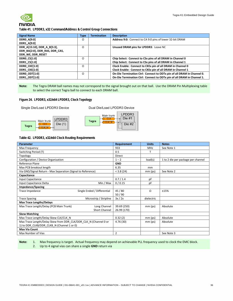
Table 43. LPDDR3, x32 Clock Connections
Signal Name Type Termination Description DDR_CLK_P/N DIFF OUT Differential Clock: Connect CLK_P/CLK_N pins of DRAM for Channel 0. DDR_CLKB_P/N DIFF OUT Differential Clock B: Connect to CLK_P/CLK_N pins of DRAM for Channel 1.
Note: DDR_COMP_PU/PD, VDDIO_DDR_HS,DRAM VREF_DQ/CA & ZQ routing requirements can be found at the end of the DDR3L section
Table 44. Miscellaneous Tegra LPDDR3 Connections
Ball Name Type Termination Description DDR_COMP_PU A 40.2Ω, 1% to VDDIO_DDR DRAM Compensation Pull-up. See termination requirement DDR_COMP_PD A 40.2Ω, 1% to GND DRAM Compensation Pull-down: See termination requirement VDDIO_DDR P DRAM Interface I/O Power Rail: Connect to 1.2V supply VDDIO_DDR_HS P DRAM Interface High Speed Power Rail: Connect to 1.05V supply
Table 45. Miscellaneous LPDDR3 Connections
Ball Name Type Termination Description VREF(CA) VREF(DQ)
A Resistor divider. One end to 1.2V & other to GND. See note under Connection diagram.
LPDDR3 Command/Address & Data Voltage References: Connect both VREF(CA) and VREF(DQ) pins of module each to center of voltage divider described in Termination column.
VDD1 P LPDDR3 Core 1: Connect VDD1 pins of module to 1.8V supply VDD2, VDDCA, VDDQ P DRAM Core 2, Command/Address/Data IO rails: Connect to 1.2V supply ZQ0, ZQ1 A 240Ω, 1% to GND LPDDR3 Zero Compensation pins: Connect each ZQ[1:0] pin to a
separate resistor and then to GND as described in Termination column VSS, VSSQ. VSSCA P LPDDR3 Core, Cmd/Add & Data GND pins: Connect to GND.
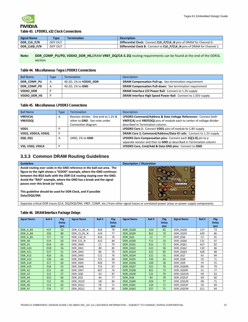
3.3.3 Common DRAM Routing Guidelines Guideline Description / Illustration Avoid routing over voids in the GND reference in the ball-out area. The figure to the right shows a “GOOD” example, where the GND continues between the BGA balls with the DDR CLK routing staying over the GND. Avoid the “BAD” example, where the GND has a break and the signal passes over this break (or Void). This guideline should be used for DDR Clock, and if possible Data/DQS/DM.
Separate critical DDR traces (CLK, DQ/DQS/DM, VREF, COMP, etc.) from other signal traces or unrelated power areas or power supply components
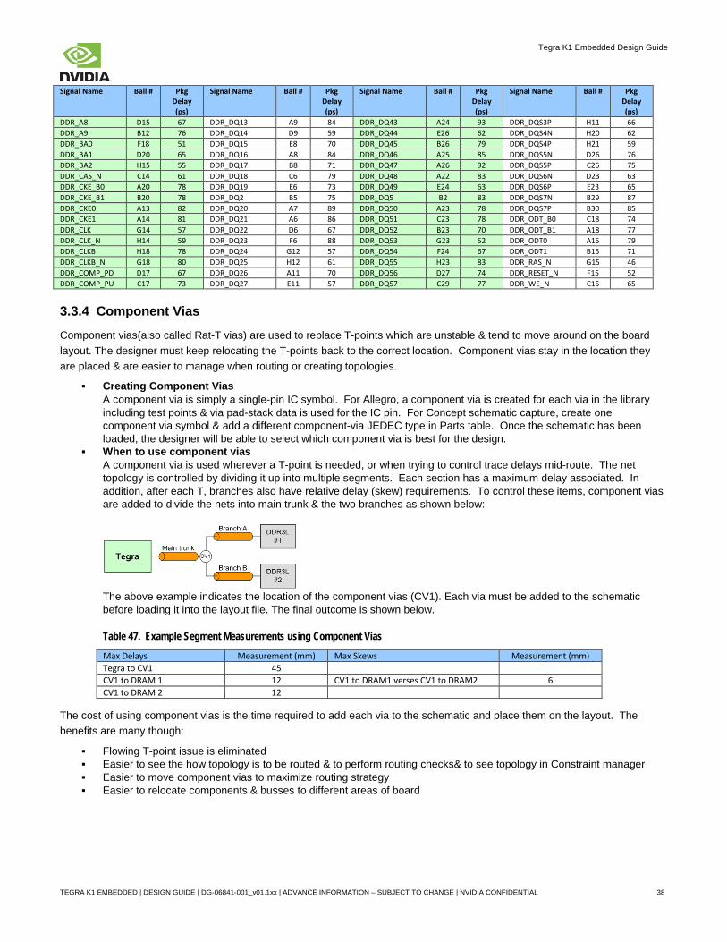
Table 46. DRAM Interface Package Delays Signal Name Ball # Pkg
Component vias(also called Rat-T vias) are used to replace T-points which are unstable & tend to move around on the board layout. The designer must keep relocating the T-points back to the correct location. Component vias stay in the location they are placed & are easier to manage when routing or creating topologies.
Creating Component Vias A component via is simply a single-pin IC symbol. For Allegro, a component via is created for each via in the library including test points & via pad-stack data is used for the IC pin. For Concept schematic capture, create one component via symbol & add a different component-via JEDEC type in Parts table. Once the schematic has been loaded, the designer will be able to select which component via is best for the design.
When to use component vias A component via is used wherever a T-point is needed, or when trying to control trace delays mid-route. The net topology is controlled by dividing it up into multiple segments. Each section has a maximum delay associated. In addition, after each T, branches also have relative delay (skew) requirements. To control these items, component vias are added to divide the nets into main trunk & the two branches as shown below:
The above example indicates the location of the component vias (CV1). Each via must be added to the schematic before loading it into the layout file. The final outcome is shown below.
Table 47. Example Segment Measurements using Component Vias
Max Delays Measurement (mm) Max Skews Measurement (mm) Tegra to CV1 45 CV1 to DRAM 1 12 CV1 to DRAM1 verses CV1 to DRAM2 6 CV1 to DRAM 2 12
The cost of using component vias is the time required to add each via to the schematic and place them on the layout. The benefits are many though:
Flowing T-point issue is eliminated Easier to see the how topology is to be routed & to perform routing checks& to see topology in Constraint manager Easier to move component vias to maximize routing strategy Easier to relocate components & busses to different areas of board
TEGRA K1 EMBEDDED | DESIGN GUIDE | DG-06841-001_v01.1xx | ADVANCE INFORMATION – SUBJECT TO CHANGE | NVIDIA CONFIDENTIAL 38
Tegra K1 Embedded Design Guide
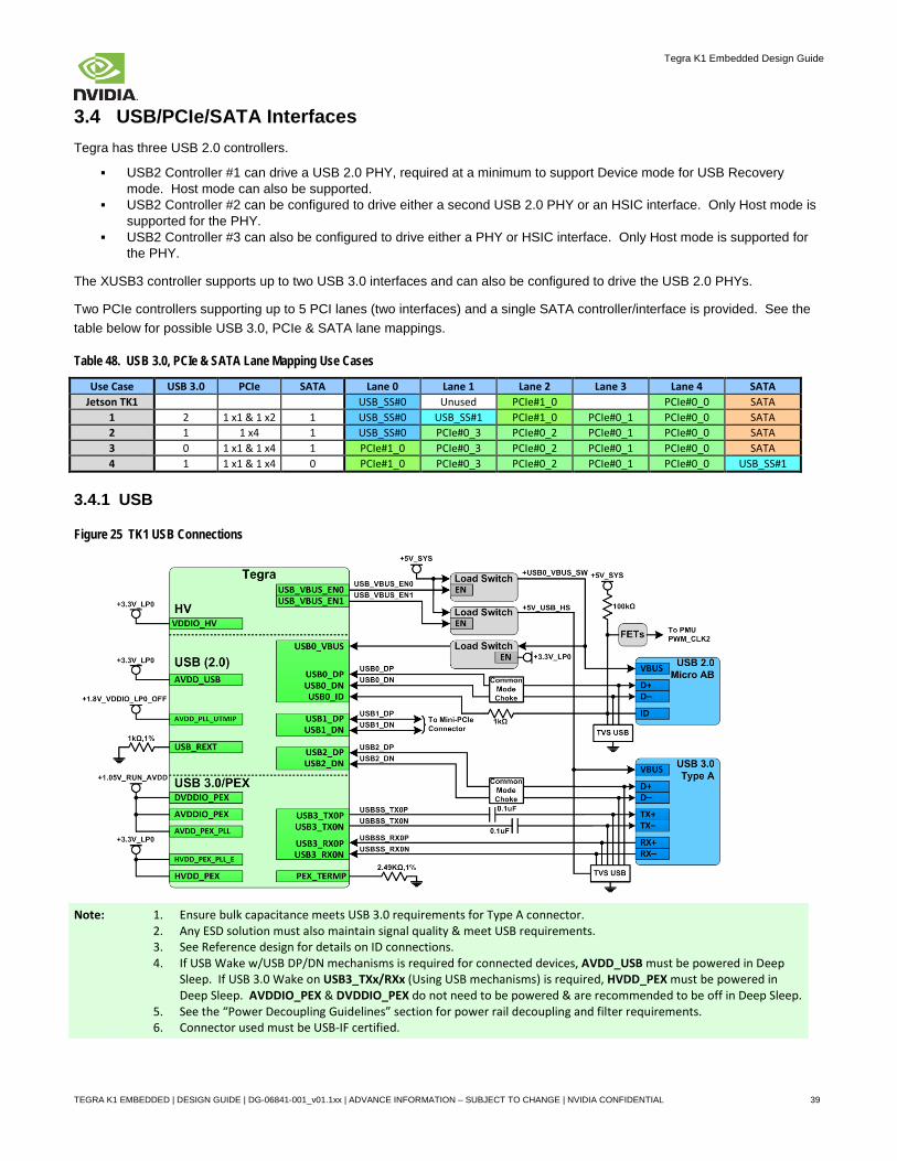
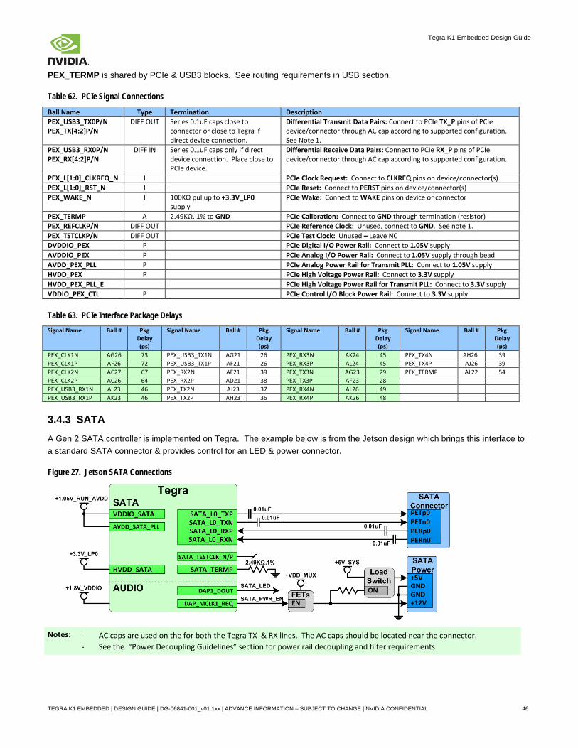
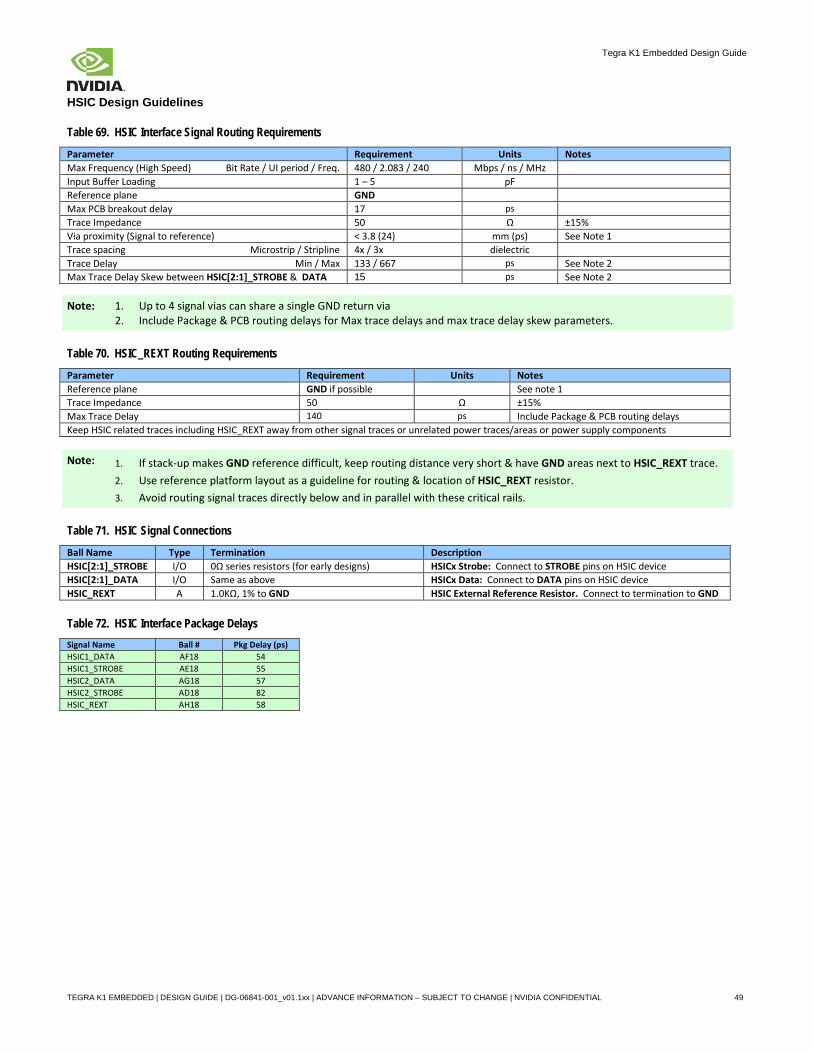
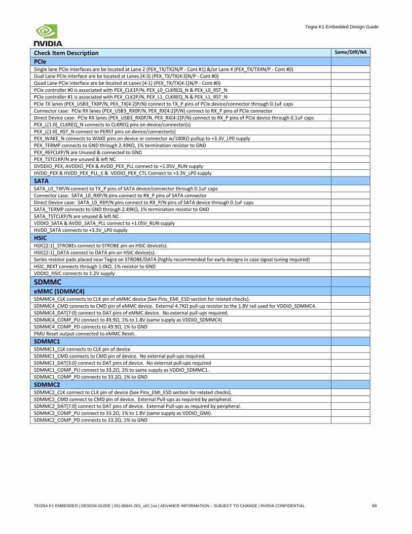
3.4 USB/PCIe/SATA Interfaces Tegra has three USB 2.0 controllers.
USB2 Controller #1 can drive a USB 2.0 PHY, required at a minimum to support Device mode for USB Recovery mode. Host mode can also be supported.
USB2 Controller #2 can be configured to drive either a second USB 2.0 PHY or an HSIC interface. Only Host mode is supported for the PHY.
USB2 Controller #3 can also be configured to drive either a PHY or HSIC interface. Only Host mode is supported for the PHY.
The XUSB3 controller supports up to two USB 3.0 interfaces and can also be configured to drive the USB 2.0 PHYs.
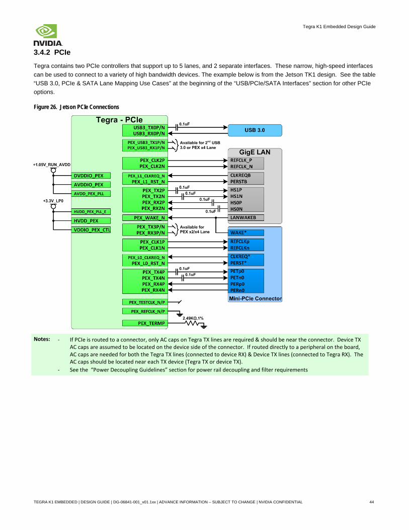
Two PCIe controllers supporting up to 5 PCI lanes (two interfaces) and a single SATA controller/interface is provided. See the table below for possible USB 3.0, PCIe & SATA lane mappings.
Table 48. USB 3.0, PCIe & SATA Lane Mapping Use Cases
Use Case USB 3.0 PCIe SATA Lane 0 Lane 1 Lane 2 Lane 3 Lane 4 SATA Jetson TK1 USB_SS#0 Unused PCIe#1_0 PCIe#0_0 SATA
Note: 1. Ensure bulk capacitance meets USB 3.0 requirements for Type A connector. 2. Any ESD solution must also maintain signal quality & meet USB requirements. 3. See Reference design for details on ID connections. 4. If USB Wake w/USB DP/DN mechanisms is required for connected devices, AVDD_USB must be powered in Deep
Sleep. If USB 3.0 Wake on USB3_TXx/RXx (Using USB mechanisms) is required, HVDD_PEX must be powered in Deep Sleep. AVDDIO_PEX & DVDDIO_PEX do not need to be powered & are recommended to be off in Deep Sleep.
5. See the “Power Decoupling Guidelines” section for power rail decoupling and filter requirements. 6. Connector used must be USB-IF certified.
TEGRA K1 EMBEDDED | DESIGN GUIDE | DG-06841-001_v01.1xx | ADVANCE INFORMATION – SUBJECT TO CHANGE | NVIDIA CONFIDENTIAL 39
Tegra K1 Embedded Design Guide
USB 2.0 Design Guidelines
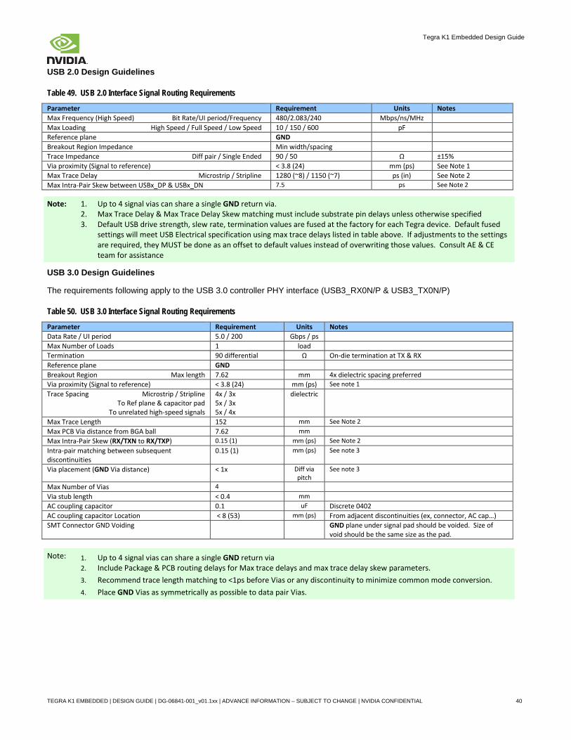
Table 49. USB 2.0 Interface Signal Routing Requirements
Parameter Requirement Units Notes Max Frequency (High Speed) Bit Rate/UI period/Frequency 480/2.083/240 Mbps/ns/MHz Max Loading High Speed / Full Speed / Low Speed 10 / 150 / 600 pF Reference plane GND Breakout Region Impedance Min width/spacing Trace Impedance Diff pair / Single Ended 90 / 50 Ω ±15% Via proximity (Signal to reference) < 3.8 (24) mm (ps) See Note 1 Max Trace Delay Microstrip / Stripline 1280 (~8) / 1150 (~7) ps (in) See Note 2 Max Intra-Pair Skew between USBx_DP & USBx_DN 7.5 ps See Note 2
Note: 1. Up to 4 signal vias can share a single GND return via. 2. Max Trace Delay & Max Trace Delay Skew matching must include substrate pin delays unless otherwise specified 3. Default USB drive strength, slew rate, termination values are fused at the factory for each Tegra device. Default fused
settings will meet USB Electrical specification using max trace delays listed in table above. If adjustments to the settings are required, they MUST be done as an offset to default values instead of overwriting those values. Consult AE & CE team for assistance
USB 3.0 Design Guidelines
The requirements following apply to the USB 3.0 controller PHY interface (USB3_RX0N/P & USB3_TX0N/P)
Table 50. USB 3.0 Interface Signal Routing Requirements
Parameter Requirement Units Notes Data Rate / UI period 5.0 / 200 Gbps / ps Max Number of Loads 1 load Termination 90 differential Ω On-die termination at TX & RX Reference plane GND Breakout Region Max length 7.62 mm 4x dielectric spacing preferred Via proximity (Signal to reference) < 3.8 (24) mm (ps) See note 1 Trace Spacing Microstrip / Stripline To Ref plane & capacitor pad To unrelated high-speed signals
4x / 3x 5x / 3x 5x / 4x
dielectric
Max Trace Length 152 mm See Note 2 Max PCB Via distance from BGA ball 7.62 mm Max Intra-Pair Skew (RX/TXN to RX/TXP) 0.15 (1) mm (ps) See Note 2 Intra-pair matching between subsequent discontinuities
0.15 (1) mm (ps) See note 3
Via placement (GND Via distance) < 1x Diff via pitch
See note 3
Max Number of Vias 4 Via stub length < 0.4 mm AC coupling capacitor 0.1 uF Discrete 0402 AC coupling capacitor Location < 8 (53) mm (ps) From adjacent discontinuities (ex, connector, AC cap…) SMT Connector GND Voiding GND plane under signal pad should be voided. Size of
void should be the same size as the pad.
Note: 1. Up to 4 signal vias can share a single GND return via 2. Include Package & PCB routing delays for Max trace delays and max trace delay skew parameters. 3. Recommend trace length matching to <1ps before Vias or any discontinuity to minimize common mode conversion. 4. Place GND Vias as symmetrically as possible to data pair Vias.
TEGRA K1 EMBEDDED | DESIGN GUIDE | DG-06841-001_v01.1xx | ADVANCE INFORMATION – SUBJECT TO CHANGE | NVIDIA CONFIDENTIAL 40
Tegra K1 Embedded Design Guide
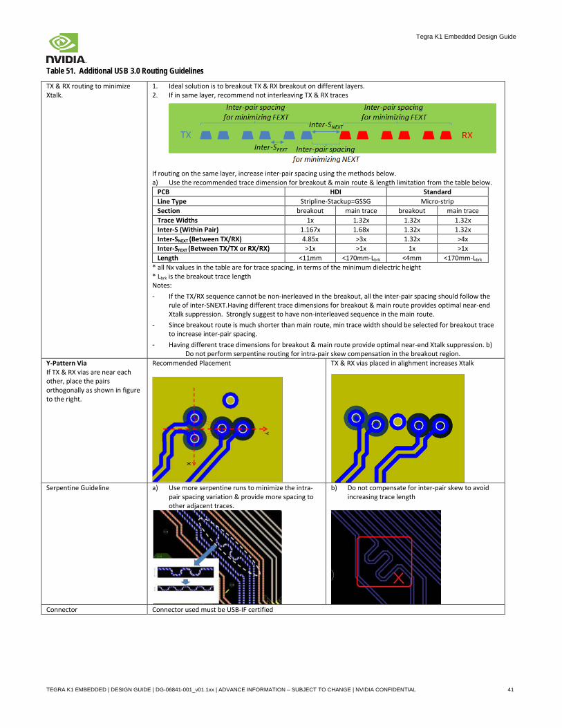
Table 51. Additional USB 3.0 Routing Guidelines
TX & RX routing to minimize Xtalk.
1. Ideal solution is to breakout TX & RX breakout on different layers. 2. If in same layer, recommend not interleaving TX & RX traces
If routing on the same layer, increase inter-pair spacing using the methods below. a) Use the recommended trace dimension for breakout & main route & length limitation from the table below.
PCB HDI Standard Line Type Stripline-Stackup=GSSG Micro-strip Section breakout main trace breakout main trace Trace Widths 1x 1.32x 1.32x 1.32x Inter-S (Within Pair) 1.167x 1.68x 1.32x 1.32x Inter-SNEXT (Between TX/RX) 4.85x >3x 1.32x >4x Inter-SFEXT (Between TX/TX or RX/RX) >1x >1x 1x >1x Length <11mm <170mm-Lbrk <4mm <170mm-Lbrk
* all Nx values in the table are for trace spacing, in terms of the minimum dielectric height * Lbrk is the breakout trace length Notes: - If the TX/RX sequence cannot be non-inerleaved in the breakout, all the inter-pair spacing should follow the
rule of inter-SNEXT.Having different trace dimensions for breakout & main route provides optimal near-end Xtalk suppression. Strongly suggest to have non-interleaved sequence in the main route.
- Since breakout route is much shorter than main route, min trace width should be selected for breakout trace to increase inter-pair spacing.
- Having different trace dimensions for breakout & main route provide optimal near-end Xtalk suppression. b) Do not perform serpentine routing for intra-pair skew compensation in the breakout region.
Y-Pattern Via If TX & RX vias are near each other, place the pairs orthogonally as shown in figure to the right.
Recommended Placement
TX & RX vias placed in alighment increases Xtalk
Serpentine Guideline a) Use more serpentine runs to minimize the intra-pair spacing variation & provide more spacing to other adjacent traces.
b) Do not compensate for inter-pair skew to avoid increasing trace length
Connector Connector used must be USB-IF certified
TEGRA K1 EMBEDDED | DESIGN GUIDE | DG-06841-001_v01.1xx | ADVANCE INFORMATION – SUBJECT TO CHANGE | NVIDIA CONFIDENTIAL 41
Tegra K1 Embedded Design Guide
Table 52. USB_REXT Routing Requirements
Parameter Requirement Units Notes Reference plane GND if possible See note 1 Trace Impedance 50 Ω ±15% Max Trace Delay 75 ps Include only PCB routing delay
Note: 1. If GND reference is not feasible, as may be the case with GSSG stack-up, keep the routing distance as short as possible & have GND areas/traces next to the USB_REXT trace.
2. Use reference platform layout as a guideline for routing & location of USB_REXT resistor. 3. Avoid routing signal traces directly below and in parallel with these critical rails.
Table 53. PEX_TERMP Routing Requirements (required for USB3 or PCIe)
Parameter Requirement Units Notes Reference plane GND if possible See note 1 Trace Impedance 50 Ω ±15% Max Trace Delay 75 ps Include only PCB routing delay
Note: 1. If GND reference is not feasible, keep the routing distance as short as possible & have GND areas/traces next to the PEX_TERMP traces.
2. Use reference platform layout as a guideline for routing & location of PEX_TERMP resistor. 3. Avoid routing signal traces directly below and in parallel with these critical rails.
Common USB Routing Guidelines
Guideline If routing to USB device or USB connector includes a flex or 2nd PCB, the total routing including all PCBs/flexes must be used for the max trace & skew calculations. Keep critical USB related traces such as USB3_TX/RX, USB_REXT & PEX_TERMP etc. away from other signal traces or unrelated power traces/areas or power supply components
Table 54. USB 2.0 Signal Connections
Ball Name Type Termination Description USB[2:0]_DP USB[2:0]_DN
DIFF I/O
90Ω common-mode chokes close to connector. ESD Protection between choke & connector on each line to GND
USB Differential Data Pair: Connect to USB Micro AB connector D+/D- pins.
USB0_VBUS
A USB Bus 5V Supply: Connect to +USB2_VBUS_SW (VBUS supply for Micro AB connector) through load switch.
USB0_ID A 100Ω series resistor. 100kΩ pull-up to +5V_SYS & ESD Protection near connector
USB Identification: Connect to USB Micro AB ID pin. Also connect ID pin from connector to PMU PWM_CLK2 pin through FETs. See reference design for details.
USB_REXT A 1KΩ, 1% to GND (see Note) External Reference: Connect through resistor to GND AVDD_USB P USB PHY Power Rail: Connect to +3.3V_LP0 supply AVDD_PLL_UTMIP P 30Ω@100MHz ferrite bead to 1.8V USB PHY PLL Power Rail: Connect to +1.8V_VDDIO_LP0_OFF supply
through filter
Table 55. USB 2.0 Interface Package Delays Signal Name Ball # Pkg Delay (ps) Signal Name Ball # Pkg Delay (ps) USB0_DN AH20 80 USB2_DN AE20 64 USB0_DP AJ20 80 USB2_DP AD20 63 USB1_DN AF20 74 USB_REXT AL19 76 USB1_DP AG20 74
TEGRA K1 EMBEDDED | DESIGN GUIDE | DG-06841-001_v01.1xx | ADVANCE INFORMATION – SUBJECT TO CHANGE | NVIDIA CONFIDENTIAL 42
Tegra K1 Embedded Design Guide
Table 56. USB 3.0 Signal Connections
Ball Name Type Termination Description USB3_TX0N/P DIFF
I/O Series 0.1uF caps close to connector. ESD Protection between cap & conn. to GND
USB 3.0 Differential Transmit Data Pair: Connect to USB 3.0 connector.
USB3_RX0N/P DIFF I/O
ESD Protection between cap & conn. to GND USB 3.0 Differential Receive Data Pairs: Connect to USB 3.0 connector.
PEX_TERMP A 2.49KΩ, 1% to GND PCIe/USB3 Calibration: Connect through resistor to GND DVDDIO_PEX P PCIe /USB PHY Digital Power Rail: Connect to 1.05V supply AVDDIO_PEX P PCIe/USB PHY Analog Power Rail: Connect to 1.05V supply AVDD_PEX_PLL P PCIe/USB PHY PLL Power Rail: Connect to 1.05V supply HVDD_PEX P PCIe/USB 3.0 High Voltage Power Rail: Connect to 3.3V supply HVDD_PEX_PLL_E P PCIe/USB 3.0 PLL High Voltage Power Rail: Connect to 3.3V supply VDDIO_PEX_CTL P PCIe/USB Control Block Rail: Connect to 3.3V supply.
Table 57. USB 3.0 ESD Protection Device Requirements
Parameter Requirement Units Notes Recommended ESD protection device SEMTECH RClamp0524p Max Reverse Stand-Off Voltage (VRWM) 5 V Any I/O pin to GND Min Reverse Breakdown Voltage (VBR) 6 V It=1mA – Any I/O pin to GND Max Reverse Leakage Current (IR) 1 uA VRWM=5V, T=25C – Any I/O pin to GND Max Clamping Voltage (VC) 15 V IPP-1A, tp=8/20us – Any I/O pin to GND Typ/Max Junction Capacitance (Cj) 0.3/0.4 pF VR=0V, f=1MHz – Between I/O pins Max Junction Capacitance (Cj) 0.8 pF VR=0V, f=1MHz – Any I/O pin to GND
Note: The junction capacitance of ESD devices has an effect on signal integrity. Choose components with low capacitance with package optimized for high speed links. SEMTECH Rclamp0524p has been well verified with its 0.3pF capacitance. See detailed characteristics above.
Table 58. USB 3.0 Common Mode Choke Requirements (Optional – Only used if rare EMI issue is seen)
Parameter Requirement Units Notes Common mode impedance (at 100MHz) Min Max
65 90
Ω
Rdc (Max) 0.3 Ω Differential mode impedance Z0 at 2.5GHz 90 Ω +/- 15% Differential insertion loss (|Sdd21| at 2.5GHz) <2.22 dB Common-to-Common insertion loss (|Scc21| at 2.5GHz) >19.2 dB
Table 59. USB 3.0 Interface Package Delays Signal Name Ball # Pkg Delay (ps) Signal Name Ball # Pkg Delay (ps) USB3_RX0N AL21 43 PEX_USB3_RX1N AL23 46 USB3_RX0P AK21 43 PEX_USB3_RX1P AK23 46 USB3_TX0N AJ21 36 PEX_USB3_TX1N AG21 26 USB3_TX0P AH21 35 PEX_USB3_TX1P AF21 26 PEX_TERMP AL22 54
Note: If the USB 3.0 interface is coming from the SATA balls, get the package delays from the table at the end of the SATA section.
TEGRA K1 EMBEDDED | DESIGN GUIDE | DG-06841-001_v01.1xx | ADVANCE INFORMATION – SUBJECT TO CHANGE | NVIDIA CONFIDENTIAL 43
Tegra K1 Embedded Design Guide
3.4.2 PCIe
Tegra contains two PCIe controllers that support up to 5 lanes, and 2 separate interfaces. These narrow, high-speed interfaces can be used to connect to a variety of high bandwidth devices. The example below is from the Jetson TK1 design. See the table “USB 3.0, PCIe & SATA Lane Mapping Use Cases” at the beginning of the “USB/PCIe/SATA Interfaces” section for other PCIe options.
Figure 26. Jetson PCIe Connections
Notes: - If PCIe is routed to a connector, only AC caps on Tegra TX lines are required & should be near the connector. Device TX AC caps are assumed to be located on the device side of the connector. If routed directly to a peripheral on the board, AC caps are needed for both the Tegra TX lines (connected to device RX) & Device TX lines (connected to Tegra RX). The AC caps should be located near each TX device (Tegra TX or device TX).
- See the “Power Decoupling Guidelines” section for power rail decoupling and filter requirements
TEGRA K1 EMBEDDED | DESIGN GUIDE | DG-06841-001_v01.1xx | ADVANCE INFORMATION – SUBJECT TO CHANGE | NVIDIA CONFIDENTIAL 44
Tegra K1 Embedded Design Guide
PCIe Design Guidelines
Table 60. PCIe Interface Signal Routing Requirements
Parameter Requirement Units Notes Max Frequency / UI Period 5.0 / 200 Gbps / ps 2.5GHz, half-rate architecture Topology Point-point Unidirectional, differential Configuration / Device Organization 1 Load Max Load (per pin) N/A pF See return loss spec in PCIe 2.0 spec Termination 50 Ω To GND Single Ended for P & N Reference plane GND Breakout Region Width/line spacing pair spacing
4 10
Mils Maximum pair spacing of 500 mils
Trace Impedance differential / Single Ended 90 45 – 60
Ω ±15%
Pair to Pair Trace Spacing Stripline / Microstrip 3x / 4x Dielectric Tx to Rx spacing Recommend Tx & Rx signals routed on separate
layers w/GND between for isolation. See note 1 Spacing to planes/cap. pads Stripline / Microstrip 3x / 4x Dielectric Max Trace Length/Delay 10” (1700) in (ps) For trace with loss <=0.4dB/in @ 2.5GHz. See
note 2 & 3 Max Within Pair Trace Delay Skew 1 ps See note 3 & 4 Max Pair to Pair Trace Delay Skew (RX to RX or TX to TX – Within Link)
600 ps See note 3 & 4
Trace Width Options 4 / 5 / 6 Mils See note 2 Note: 1. If routing in the same layer is necessary, route group TX & RX separately wo/mixing RX/TX routes & keep distance
between nearest TX/RX trace & RX to other signals 3x RX-RX separation 2. For with trace loss >= 0.7dB/in @ 2.5GHz, the max trace length should be 7.5 inches. To reduce trace loss, ensure the
loss tangent of the dielectric material & roughness of the metal are tightly controlled. 3. Include Package & PCB routing delays for Max trace delays and max trace delay skew parameters. 4. Do trace length matching before the vias to transition to different layers or any discontinuity to minimize common mode
conversion
Table 61. Additional PCIe Interface Signal Routing Guidelines
Maximum # of Vias Maximum of 4 vias per TX traces and 2 vias per RX trace. Routing signals over the antipad Not allowed Routing over voids When signal pair approaches vias, the maximal trace length across the void on the plane is 50mil; Serpentine line rule For microstrip line, minimal spacing between each turn is 4x dielectric; For stripline, it is 3x dielectric height
(3x of thinner of above & below) PTH (Plated Through-hole) Vias Keep GND via as close as possible Ground sliver between BGA pads Remove ground slivers between BGA pads & feedthrus to via to reduce the capacitive loading of BGA pad DC Blocking capacitor location Place DC blocking capacitors within 0.3” of the connector if one exists, or near the receiver. Ground plane under AC cap pads Remove GND plane under AC blocking capacitor pads. If board has ICT pads, remove plane under those as
well. Void is size of pad + ring equal to dielectric thickness.
Serpentine line rule - Avoid tight bends
- No 90deg bends; impact to loss and jitter budgets - Keep angles >= 135deg (a) - maintain adequate air gap
- A >= 4x trace width - Lengths of B, C >= 1.5x trace width - Serpetines length is at least 3w for jog
Keep critical PCIe/SATA related traces such as PCIe/SATA_TX/RX, PCIe/SATA_TERMP etc. away from other signal traces or unrelated power traces/areas or power supply components
TEGRA K1 EMBEDDED | DESIGN GUIDE | DG-06841-001_v01.1xx | ADVANCE INFORMATION – SUBJECT TO CHANGE | NVIDIA CONFIDENTIAL 45
Tegra K1 Embedded Design Guide
PEX_TERMP is shared by PCIe & USB3 blocks. See routing requirements in USB section.
Table 62. PCIe Signal Connections
Ball Name Type Termination Description PEX_USB3_TX0P/N PEX_TX[4:2]P/N
DIFF OUT Series 0.1uF caps close to connector or close to Tegra if direct device connection.
Differential Transmit Data Pairs: Connect to PCIe TX_P pins of PCIe device/connector through AC cap according to supported configuration. See Note 1.
PEX_USB3_RX0P/N PEX_RX[4:2]P/N
DIFF IN Series 0.1uF caps only if direct device connection. Place close to PCIe device.
Differential Receive Data Pairs: Connect to PCIe RX_P pins of PCIe device/connector through AC cap according to supported configuration.
PEX_L[1:0]_CLKREQ_N I PCIe Clock Request: Connect to CLKREQ pins on device/connector(s) PEX_L[1:0]_RST_N I PCIe Reset: Connect to PERST pins on device/connector(s) PEX_WAKE_N I 100KΩ pullup to +3.3V_LP0
supply PCIe Wake: Connect to WAKE pins on device or connector
PEX_TERMP A 2.49KΩ, 1% to GND PCIe Calibration: Connect to GND through termination (resistor) PEX_REFCLKP/N DIFF OUT PCIe Reference Clock: Unused, connect to GND. See note 1. PEX_TSTCLKP/N DIFF OUT PCIe Test Clock: Unused – Leave NC DVDDIO_PEX P PCIe Digital I/O Power Rail: Connect to 1.05V supply AVDDIO_PEX P PCIe Analog I/O Power Rail: Connect to 1.05V supply through bead AVDD_PEX_PLL P PCIe Analog Power Rail for Transmit PLL: Connect to 1.05V supply HVDD_PEX P PCIe High Voltage Power Rail: Connect to 3.3V supply HVDD_PEX_PLL_E PCIe High Voltage Power Rail for Transmit PLL: Connect to 3.3V supply VDDIO_PEX_CTL P PCIe Control I/O Block Power Rail: Connect to 3.3V supply
Table 63. PCIe Interface Package Delays Signal Name Ball # Pkg
A Gen 2 SATA controller is implemented on Tegra. The example below is from the Jetson design which brings this interface to a standard SATA connector & provides control for an LED & power connector.
Figure 27. Jetson SATA Connections
Notes: - AC caps are used on the for both the Tegra TX & RX lines. The AC caps should be located near the connector. - See the “Power Decoupling Guidelines” section for power rail decoupling and filter requirements
TEGRA K1 EMBEDDED | DESIGN GUIDE | DG-06841-001_v01.1xx | ADVANCE INFORMATION – SUBJECT TO CHANGE | NVIDIA CONFIDENTIAL 46
Tegra K1 Embedded Design Guide
Table 64. SATA Signal Routing Requirements
Parameter Requirement Units Notes Max Frequency Bit Rate / UI 3.0 / 333.3 Gbps / ps 1.5GHz Topology Point to point,
unidirectional, differential
Configuration / Device Organization 1 load Max Load (per pin) 0.5 pf Termination 100 Ω On die termination Reference plane GND Breakout Region Impedance Trace Width / Line separation 4
4 mils
Trace Impedance Differential Pair / Single Ended 90 55
Ω ±15%
Pair to Pair Trace Spacing Stripline / Microstrip 3x / 3x Dielectric Max Trace Delay 1360 (8) ps (in) See Note 1 & 2 Max Intra-Pair Trace Delay Skew 1 ps See Note 1 & 2 Keep critical PCIe/SATA related traces such as PCIe/SATA_TX/RX, PCIe/SATA_TERMP etc. away from other signal traces or unrelated power traces/areas or power supply components Note: 1. If routing to SATA device or SATA connector includes a flex or 2nd PCB, the total routing including all PCBs/flexes must be
used for the max trace & skew calculations 2. Include Package & PCB routing delays for Max trace delays and max trace delay skew parameters.
Table 65. SATA_TERMP Routing Requirements
Parameter Requirement Units Notes Reference plane GND Trace Impedance 50 Ω ±15% Max Trace Delay 75 ps Include only PCB routing delay
Table 66. Additional SATA Interface Signal Routing Guidelines
Preferred routing layer for through-hole SATA Connector
Place AC caps on bottom layer if possible. PCB trace connecting AC cap & SATA connector should be on bottom layer as microstrip. PCB trace connecting the Chip to the AC caps should be on the top layer
In case AC cap has to be put on the top layer because of design constraints then the PCB trace connecting the connector to the AC cap should be on the bottom layer as shown below.
Preferred routing layer for SMT SATA Connector
For SMT connector AC caps should be on top layer. PCB trace connecting AC caps & SATA connector, & Tegra to AC caps should be on top layer as microstrip.
Recommendations for SMT Connector
GND plane under signal pad should be voided for better differential mode & common mode return loss. Size of void should be 5 mils larger than SMT SATA connector pad in each direction.
TEGRA K1 EMBEDDED | DESIGN GUIDE | DG-06841-001_v01.1xx | ADVANCE INFORMATION – SUBJECT TO CHANGE | NVIDIA CONFIDENTIAL 47
Tegra K1 Embedded Design Guide
If space is available, use 2 GND vias for 1 GND pad to decrease differential-mode far-end cross-talk, as well as mode conversion when void is enlarged as described above.
Delay Matching Do trace delay matching before the vias to transition to different layers Maximal # of vias Maximum of 4 vias per TX traces and 2 vias per RX trace Routing over voids Where signal pair approaches vias, maximal trace length across void on plane is 1.27mm Serpentine line rule For microstrip line, minimal spacing between each turn is 4x dielectric; For stripline, it is 3x dielectric height (3x of
thinner of above & below) DC Blocking capacitor location Place DC blocking capacitors less than 12.5mm from connector. DC Blocking capacitor GND removal
Remove plane underneath the DC blocking capacitor pads. If board has ICT pads, remove plane under those as well. Void is size of pad + ring equal to dielectric thickness.
Anti-pad for connector pin Not required if PCB trace connecting AC cap & connector is on bottom layer. In case PCB trace connecting AC cap & connector is on top layer, increase size of anti-pads for connector pins to 35mm & void out ground planes whenever there are solder pads
Table 67. SATA Signal Connections
Ball Name Type Termination Description SATA_L0_TXP/N DIFF OUT Series 0.01uF caps close to
connector or close to Tegra if direct device connection.
Differential Transmit Data Pair: Connect to SATAN/P/pins of SATA device/connector through termination (capacitor)
SATA_L0_RXP/N DIFF IN Series 0.01uF caps only if direct device connection. Place close to SATA device.
Differential Receive Data Pair: Connect to SATAN/P pins of SATA device/connector through termination (capacitor)
SATA_TERMP A 2.49KΩ, 1% to GND SATA Calibration: Connect to GND through termination (resistor) SATA_TSTCLKP/N DIFF OUT SATA Test Clock: Unused – Leave NC VDDIO_SATA P SATA I/O Power Rail: Connect to 1.05V supply. AVDD_SATA_PLL P SATA Analog Power Rail for Transmit PLL: Connect to 1.05V supply HVDD_SATA P SATA High Voltage Power Rail: Connect to 3.3V supply
Table 68. SATA Interface Package Delays Signal Name Ball # Pkg Delay (ps) Signal Name Ball # Pkg Delay (ps) SATA_L0_RXN AH27 44 SATA_L0_TXN AK27 50 SATA_L0_RXP AJ27 44 SATA_L0_TXP AL27 49 SATA_TERMP AL25 55
3.4.4 HSIC
Tegra supports two HSIC interfaces. These 2-pin, 1.2V CMOS interfaces can connect to compatible modems, Wi-Fi controllers, USB PHYs, etc. The example below from the Jetson design brings the HSIC1 interface to the General Expansion Header.
Figure 28. Jetson HSIC connections
Note: - VDDIO_HSIC must remain powered in Deep Sleep if connected device must maintain connection. Powering off/on VDDIO_HSIC will require re-enumeration of the HSIC interface.
- Series resistors near Tegra are recommended for early builds for use as test points, or possible signal conditioning - See the “Power Decoupling Guidelines” section for power rail decoupling and filter requirements
TEGRA K1 EMBEDDED | DESIGN GUIDE | DG-06841-001_v01.1xx | ADVANCE INFORMATION – SUBJECT TO CHANGE | NVIDIA CONFIDENTIAL 48
Tegra K1 Embedded Design Guide
HSIC Design Guidelines
Table 69. HSIC Interface Signal Routing Requirements
Parameter Requirement Units Notes Max Frequency (High Speed) Bit Rate / UI period / Freq. 480 / 2.083 / 240 Mbps / ns / MHz Input Buffer Loading 1 – 5 pF Reference plane GND Max PCB breakout delay 17 ps Trace Impedance 50 Ω ±15% Via proximity (Signal to reference) < 3.8 (24) mm (ps) See Note 1 Trace spacing Microstrip / Stripline 4x / 3x dielectric Trace Delay Min / Max 133 / 667 ps See Note 2 Max Trace Delay Skew between HSIC[2:1]_STROBE & DATA 15 ps See Note 2
Note: 1. Up to 4 signal vias can share a single GND return via 2. Include Package & PCB routing delays for Max trace delays and max trace delay skew parameters.
Table 70. HSIC_REXT Routing Requirements
Parameter Requirement Units Notes Reference plane GND if possible See note 1 Trace Impedance 50 Ω ±15% Max Trace Delay 140 ps Include Package & PCB routing delays Keep HSIC related traces including HSIC_REXT away from other signal traces or unrelated power traces/areas or power supply components
Note: 1. If stack-up makes GND reference difficult, keep routing distance very short & have GND areas next to HSIC_REXT trace. 2. Use reference platform layout as a guideline for routing & location of HSIC_REXT resistor. 3. Avoid routing signal traces directly below and in parallel with these critical rails.
Table 71. HSIC Signal Connections
Ball Name Type Termination Description HSIC[2:1]_STROBE I/O 0Ω series resistors (for early designs) HSICx Strobe: Connect to STROBE pins on HSIC device HSIC[2:1]_DATA I/O Same as above HSICx Data: Connect to DATA pins on HSIC device HSIC_REXT A 1.0KΩ, 1% to GND HSIC External Reference Resistor. Connect to termination to GND
TEGRA K1 EMBEDDED | DESIGN GUIDE | DG-06841-001_v01.1xx | ADVANCE INFORMATION – SUBJECT TO CHANGE | NVIDIA CONFIDENTIAL 49
Tegra K1 Embedded Design Guide
3.5 Display Tegra supports eDP, LVDS or DSI for embedded displays as well as HDMI for external displays. The Jetson TK1 design provides access to the eDP/LVDS display options on the Display/Touch Expansion header.
Figure 29: Jetson Display Block Diagram
3.5.1 eDP/LVDS
Jetson supports up to a 4-lane single-link LVDS interface or up to a 4-lane eDP interface. The maximum resolution supported with LVDS is 1920x1200 @ 60fps (24bpp color depth). With eDP, the maximum supported using the full 4 lanes is 3840x2160 @ 60fps. LVDS and eDP are multiplexed on the same pins. See LVDS/eDP Pin Assignment Options table below for pin assignments for each interface.
Table 73. eDP/LVDS Pin Assignment Options
Tegra Ball LVDS (3-lane) LVDS (4 lane) eDP LVDS0_TXD0_P/N LVDS lane 0 LVDS lane 0 eDP lane 2 LVDS0_TXD1_P/N LVDS lane 1 LVDS lane 1 eDP lane 1 LVDS0_TXD2_P/N LVDS lane 2 LVDS lane 2 eDP lane 0 LVDS0_TXD3_P/N N/A LVDS lane 3 N/A LVDS0_TXD4_P/N LVDS clock lane LVDS clock lane eDP lane 3
TEGRA K1 EMBEDDED | DESIGN GUIDE | DG-06841-001_v01.1xx | ADVANCE INFORMATION – SUBJECT TO CHANGE | NVIDIA CONFIDENTIAL 50
Tegra K1 Embedded Design Guide
Figure 30: eDP 4-Lane Connection Example
Notes: - Filters on the DSI signals are not recommended. If EMI is a concern, other solutions, such as using PCB GND layers or other shielding is preferred. If EMI devices are necessary, they must be tuned to minimize the impact to signal quality, which must meet the timing & Vil/Vih requirements at the receiver & not introduce glitches on the signal edges. Any ESD solution must also maintain signal quality and meet requirements for the frequencies supported by the design.
- See the “Power Decoupling Guidelines” section for power rail decoupling and filter requirements.
Figure 31: LVDS 4-Lane Connection Example
Note: - Filters on the DSI signals are not recommended. If EMI is a concern, other solutions, such as using PCB GND layers or other shielding is preferred. If EMI devices are necessary, they must be tuned to minimize the impact to signal quality, which must meet the timing & Vil/Vih requirements at the receiver & not introduce glitches on the signal edges. Any ESD solution must also maintain signal quality and meet requirements for the frequencies supported by the design.
- See the “Power Decoupling Guidelines” section for power rail decoupling and filter requirements.
TEGRA K1 EMBEDDED | DESIGN GUIDE | DG-06841-001_v01.1xx | ADVANCE INFORMATION – SUBJECT TO CHANGE | NVIDIA CONFIDENTIAL 51
Tegra K1 Embedded Design Guide
eDP Design Guidelines
Table 74. eDP (HBR2) Main Link Signal Routing Requirements
Parameter Requirement Units Notes Max Data Rate (per data lane) HBR2 / HBR / RBR 5.4 / 2.7 / 1.62 Gbps Min UI HBR2 / HBR / RBR 185 / 370 / 617 ps Number of Loads 1 load Topology Point-Point, Differential, Unidirectional Termination 100 Ω On die at TX/RX Reference plane GND Max PCB breakout length 7.63 (0.3) mm (in) Trace Impedance Diff pair / Single Ended 90 / 45-60 Ω ±15% Stripline Routing for Main Trunk
Max trace length from Tegra TX pin to connector RBR/HBR HBR2 Max Propagation Delay – HBR2
215 (8.5) 165 (6.5) 1137
mm (in) mm (in) ps
See Note 1 175ps/inch delay assumption for stripline
Max number of signal vias RBR,HBR / HBR2 4 / 2 HBR2: One more test via right after AC cap OK PCB pair-to-pair spacing 3x dielectric height 3x of the thinner of above and below PCB main link to AUX Spacing 3x dielectric height 3x of the thinner of above and below Max stub length on the Vias Allowed Rout below core to minimize stub length
Microstrip Routing for Main Trunk Max trace length from Tegra TX pin to connector RBR/HBR HBR2 (5x / 7x spacing) Max Propagation Delay – HBR2 (5x / 7x spacing)
215 (8.5) 127 (5) / 152.4 (6) 750 / 900
mm (in) mm (in) ps
See Note 1 150ps/inch delay assumption for microstrip
Max number of signal vias RBR,HBR / HBR2 4 / 2 HBR2: One more test via right after AC cap OK
PCB pair-pair spacing RBR,HBR / HBR2 4x / 5x-7x dielectric height PCB main link to AUX Spacing 5x dielectric height
Signal Skews (Stripline or Microstrip) Max Intra-pair (within pair) Skew 1 ps See Note 1 & 2 Max Inter-pair (pair-pair) Skew 150 ps See Note 1 & 2
Note: - Max Trace Delay & Max Trace Delay Skew matching must include substrate pin delays unless otherwise specified - Recommend doing trace length matching to <1ps before vias or any discontinuity to minimize common mode conversion
Parameter Requirement Units Notes Max PCB via distance from BGA RBR/HBR HBR2
No requirement 7.63 (0.3)
mm (in)
Max signal transition vias 2 Recommend </= 2 for predominately stripline routing & </=n 4 for predominately microstrip routing.
Main Trunk routing Stripline Recommended Max GND transition via distance < 1x diff pair
pitch For signals switching reference layers, add symmetrical ground stitching via near signal vias.
AC coupling cap 100 nF Discrete 0402 Max Distance from AC cap to conn. RBR/HBR HBR2
No requirement 0.5
in
RBR and HBR: no requirement HBR2: less than 0.5 inch
AC cap pad voiding RBR/HBR HBR2
No voiding required Voiding required
HBR2: Voiding the plane directly under the pad 3-4 mils larger than the pad size is recommended.
Connector voiding RBR/HBR HBR2
No voiding required Voiding required
HBR2: Standard DP Connector: Voiding requirement is stack-up dependent. For typical stack-ups, voiding on the layer under the connector pad is recommended to be 5.7mil larger than the connector pad.
ESD protection device ESD protection required to meet device testing beyond 2kV HMM (human metal model) direct pin injection test.
TEGRA K1 EMBEDDED | DESIGN GUIDE | DG-06841-001_v01.1xx | ADVANCE INFORMATION – SUBJECT TO CHANGE | NVIDIA CONFIDENTIAL 52
Tegra K1 Embedded Design Guide
Table 76. eDP Auxiliary Channel Signal Routing Requirements
Parameter Requirement Units Notes Termination, Reference plane, Max breakout, Impedance, Max trace length, Max Vias
Same as Main Link
PCB pair-to-pair spacing Stripline/Microstrip 2x/3x dielectric height Max Intra-pair (within pair) Skew Same as Main Link Max Inter-pair (pair-pair) Skew No requirement
Table 77. LVDS Signal Routing Requirements
Parameter Requirement Units Notes Max Frequency / Bit Rate 135 / 945 MHz / Mbps Number of Loads 1 load Topology Point-Point or Multi-drop, Differential, Unidirectional Termination 100 Ω At the receiver (on die or on board) Reference Plane GND Trace Impedance Diff pair / Single Ended 90 / 45-55 Ω ±15% Max Trace Length Stripline / Microstrip 10 / 12 in See Note 1 PCB pair-to-pair spacing Stripline / Microstrip 3x / 4x dielectric height 3x of the thinner of above and below Max Intra-pair (within pair) Skew 5 ps See Note 1 Max Inter-pair (pair-pair) Skew 100 ps See Note 1
Note: Include Package & PCB routing delays for Max trace delays and max trace delay skew parameters.
Table 78. LVDS Multi-drop Signal Routing Requirements
Parameter Requirement Units Notes Stub length < 15 % (of rise time) External termination resistor 100 Ω Placed at the far end (last receiver). On chip termination receiver 90 ≤ ZL ≤ 132 Ω Total load
Table 79. LVDS0_RSET Routing Requirements
Parameter Requirement Units Notes Reference plane GND if possible See note 1 Trace Impedance 50 Ω ±15% Max Trace Delay 40 ps Include only PCB routing delay
Note: If stack-up makes GND reference difficult, keep routing distance very short & have GND areas next to LVDS0_RSET trace.
Common eDP/LVDS Routing Guidelines
Guideline If routing to eDP or LVDS device includes a flex or 2nd PCB, the max trace & skew calculations must include all the PCBs/flex routing Keep critical eDP/LVDS related traces including differential clock/data traces & RSET trace away from other signal traces or unrelated power traces/areas or power supply components
Table 80. eDP Signal Connections
Ball Name Type Termination Description LVDS0_TXD[4:0]_P/N O eDP: Series 0.1uF capacitors eDP/LVDS CLK/Data Lanes: See eDP/LVDS Pin Assignment Options
table or diagrams for correct connection to display connector. LVDS0_RSET A 1KΩ, 1% to GND eDP Current Reference: Connect to resistor to GND. AVDD_LVDS0_IO P Note 1 eDP IO Power Rail: Connect to 1.05V supply AVDD_LVDS0_PLL P Note 1 eDP Dedicated PLL Power Rail: Connect to 3.3V supply for eDP DP_AUX_CH0_P/N O 100KΩ pull-downs on both lines near Tegra,
series 0.1uF capacitors, then 100KΩ pull-down on AUX_P & 100KΩ pull-up on AUX_N.
eDP Auxiliary Channel: Connect to AUX_CH_P/N on display connector.
DP_HPD I/OD eDP Hot Plug Detect: Connect to HPD on display connector.
Note: - DP_AUX_CH0_P/N (I2C6) & DP_HPD only supported when IF block powered by VDDIO_HV is from 2.8-3.3V.
TEGRA K1 EMBEDDED | DESIGN GUIDE | DG-06841-001_v01.1xx | ADVANCE INFORMATION – SUBJECT TO CHANGE | NVIDIA CONFIDENTIAL 53
Tegra K1 Embedded Design Guide
Table 81. LVDS Signal Connections
Ball Name Type Termination Description LVDS0_TXD[4:0]_P/N O LVDS CLK/Data Lanes: See eDP/LVDS Pin Assignment Options
table or diagrams for correct connection to display connector. LVDS0_RSET A 1KΩ, 1% to GND LVDS Current Reference: Connect to resistor to GND. AVDD_LVDS0_IO P Note 1 LVDS IO Power Rail: Connect to 1.05V supply AVDD_LVDS0_PLL P Note 1 LVDS Dedicated PLL Power Rail: Connect to 1.8V for LVDS.
Tegra supports eight total MIPI DSI data lanes and two clock lanes, allowing up to two 4-lane interfaces. Each data channel has peak bandwidth up to 1.5Gbps.
Additional Functions:
Tearing Effect input to allow the display controller to synchronize to panel drivers with their own timing controllers. Backlight PWM Various GPIOs to support display power sequencing, power management, etc.
Figure 32: DSI 2 x 4-Lane Connection Example
Note: - Filters on the DSI signals are not recommended. If EMI is a concern, other solutions, such as using PCB GND layers or other shielding is preferred. If EMI devices are necessary, they must be tuned to minimize the impact to signal quality, which must meet the timing & Vil/Vih requirements at the receiver & not introduce glitches on the signal edges. Any ESD solution must also maintain signal quality and meet requirements for the frequencies supported by the design.
- See the “Power Decoupling Guidelines” section for power rail decoupling and filter requirements.
TEGRA K1 EMBEDDED | DESIGN GUIDE | DG-06841-001_v01.1xx | ADVANCE INFORMATION – SUBJECT TO CHANGE | NVIDIA CONFIDENTIAL 54
Tegra K1 Embedded Design Guide
MIPI DSI and CSI Design Guidelines
Table 83. MIPI DSI & CSI Interface Signal Routing Requirements
Parameter Requirement Units Notes Max Frequency/Data Rate (per data lane) 750 / 1500 MHz/Mbps Number of Loads / Max Loading (per pin) 1 / 10 Load / pf Reference plane GND or PWR See Note 1 Breakout Region Impedance Diff pair / Single Ended 90 / 45-55 Ω ±15% Max PCB breakout delay 48 ps Trace Impedance Diff pair / Single Ended 90 / 45-55 Ω Via proximity (Signal to reference) < 3.8 (24) mm (ps) See Note 2 Trace spacing Microstrip / Stripline 2x / 2x dielectric Max Trace Delay 1620 ps See Note 3 Max Intra-pair Skew 1 ps See Note 3 Max Trace Delay Skew between DQ & CLK 10 ps See Note 3 If routing to DSI or CSI device includes a flex or 2nd PCB, the max trace & skew calculations must include all the PCBs/flex routing Keep critical DSI/CSI related traces including DSI/CSI clock/data traces & RDN/RUP traces away from other signal traces or unrelated power traces/areas or power supply components
Note: 1. If PWR, 0.01uF decoupling cap required for return current 2. Up to 4 signal vias can share a single GND return via 3. Include Package & PCB routing delays for Max trace delays and max trace delay skew parameters.
Table 84. CSI_DSI_RDN/RUP Routing Requirements
Parameter Requirement Units Notes Reference plane GND if possible See note 1 Trace Impedance 50 Ω ±15% Max Trace Delay 40 ps Include only PCB routing delay
Note: 1. If stack-up makes GND reference difficult, keep routing distance very short & have GND areas next to CSI_DSI_RDN/RUP traces.
2. Use reference platform layout as a guideline for routing & location of CSI_DSI_RDN/RUP resistors. 3. Avoid routing signal traces directly below and in parallel with these critical rails.
Table 85. MIPI DSI Signal Connections
Ball Name Type Termination Description DSI_A_CLK_N/P O DSI Differential A Clock: Connect to CLKn & CLKp pins of receiver DSI_A_D[3:0]_N/P I/O DSI Differential A Data Lanes: Connect to up to 4 sets of Dn & Dp pins of
Primary DSI display DSI_B_CLK_N/P O Differential B Clock: Connect to CLKn & CLKp pins of secondary receiver DSI_B_D[3:0]_N/P I/O Differential B Data Lanes: Connect to up to 4 sets of Dn & Dp pins of
secondary DSI display, or second set of 4 lanes to primary display. CSI_DSI_RDN A 49.9Ω, 1% to GND DSI/CSI Voltage Reference Pulldown: CSI_DSI_RUP A 453Ω, 1% to 1.2V DSI/CSI Voltage Reference Pull-up: AVDD_CSI_DSI P MIPI DSI & CSI Shared Power Rail: Connect to 1.2V supply
Table 86. DSI Interface Package Delays Signal Name Ball # Pkg
TEGRA K1 EMBEDDED | DESIGN GUIDE | DG-06841-001_v01.1xx | ADVANCE INFORMATION – SUBJECT TO CHANGE | NVIDIA CONFIDENTIAL 55
Tegra K1 Embedded Design Guide
3.5.3 HDMI
A standard HDMI V1.4b interface is supported.
Figure 33: HDMI Connection Example
Note: 1. The backdrive block associated w/AVDD_HDMI is used to prevent current passing back through Tegra when the 3.3V supply is off, but the device is connected to a powered display.
2. Any ESD solution must also maintain signal integrity & meet the HDMI requirements for the modes to be supported 3. Ensure AVDD_HDMI supply can handle >= 100mA as there can be an increase in power consumption for ~1second when
the HDMI cable is unplugged from the display device before SW has a chance to disable the HDMI pads. 4. Filters on HDMI Clock/Data lines are not recommended. If EMI devices are necessary, they must be tuned to maximize
signal quality, which must meet the HDMI specification for the modes to be supported. 5. See the “Power Decoupling Guidelines” section for power rail decoupling and filter requirements
TEGRA K1 EMBEDDED | DESIGN GUIDE | DG-06841-001_v01.1xx | ADVANCE INFORMATION – SUBJECT TO CHANGE | NVIDIA CONFIDENTIAL 56
Tegra K1 Embedded Design Guide
HDMI Design Guidelines
Figure 34: HDMI Differential Clock & Data Topology
Table 87. HDMI Interface Signal Routing Requirements
Parameter Requirement Units Notes Max Frequency 297 MHz Data rate (1/UI) is ten times larger than
the pixel frequency (1/T_pixel) Topology Point to point Termination At Receiver On-board
50 500
Ω To 3.3V at receiver To GND near connector
Reference plane GND Max Breakout Length / Delay 7.62 (52.5) mm (ps) Trace Impedance Diff pair / Single Ended 90 / 45-60 Ω ±15% Trace spacing Microstrip / Stripline 4x / 3x dielectric See Note 1 Max Trunk Delay (297) Microstrip Stripline
114/4.5 (675) 114/4.5 (787)
mm/in (ps) See Note 2 & 3
Max Trunk Delay (225) Microstrip Stripline
254/10 (1500) 204/8 (1400)
mm/in (ps) See Note 2 & 3
Max Trunk Delay (165) Microstrip Stripline
320/12.5 (1870) 254/10 (1500)
mm/in (ps) See Note 2 & 3
Max distance from ESD to connector (Seg A) 12.7 (87) mm (ps) Max distance from signal line to ESD pad (Seg B) 6.35 (37.5) mm (ps) Keep stub connecting ESD to signal trace
very short or overlay pad on signal trace. See example layout figure below table)
Max Intra-Pair (within pair) Skew 1 ps See Note 2 & 3 Max Inter-Pair (pair to pair) Skew 150 ps See Note 2 & 3
Note: 1. Microstrip routing is recommended for HDMI due to limited eye height and has longer MAX length 2. Include Package & PCB routing delays for Max trace delays and max trace delay skew parameters. 3. If routing to HDMI connector includes a flex or 2nd PCB, the max trace delay & skew calculations must include all the
PCBs/flex routing
Figure 35: Example HDMI high-speed trace & component layout
TEGRA K1 EMBEDDED | DESIGN GUIDE | DG-06841-001_v01.1xx | ADVANCE INFORMATION – SUBJECT TO CHANGE | NVIDIA CONFIDENTIAL 57
Parameter Requirement Units Notes Max signal transition vias 2 Recommend </= 2 for predominately stripline routing & </=n 4 for
predominately microstrip routing. Stripline routing Recommend routing near bottom layer to minimize via stub lengths GND transition via < 1x diff pair
pitch For signals switching reference layers, add symmetrical ground stitching via near signal vias. GND via distance should be < 1X diff pair via pitch
Padstack of signal via (pad/drill/antipad) 0.45/0.25/0.86 mm Recommended to reduce capacitance and loss (Guideline intended for PTH – Plated Through-Hole Vias)
Connector voiding Voiding GND below the signal lanes 5.7mil larger than the pin itself is recommended (see figure)
ESD protection device ESD protection required to meet device testing beyond 2kV HMM (human metal model) direct pin injection test.
Filter Capacitor on 5V 100 pF 0402 size capacitor on the 5V output is required for EMI reduction Routing Over void not allowed Exception is anti-pad at connector pins which causes voids. Route traces
w/min. void references. Routing away from sources of noise Keep critical HDMI related traces including differential clock/data traces &
RSET trace away from other signal traces or unrelated power traces/areas or power supply components
Table 89. HDMI_RSET Routing Requirements
Parameter Requirement Units Notes Reference plane GND if possible See note 1 Trace Impedance 50 Ω ±15% Trace Spacing 2x dielectric Max Trace Delay 75 ps Include only PCB routing delay
Note: 1. If stack-up makes GND reference difficult, keep routing distance very short & have GND areas next to HDMI_RSET trace. 2. Use reference platform layout as a guideline for routing & location of HDMI_RSET resistor. 3. Avoid routing signal traces directly below and in parallel with these critical rails.
Table 90. HDMI Signal Connections
Ball Name Type Termination (see note on ESD) Description HDMI_TXCN/P O HDMI Differential Clock: Connect to CN/CP pins on HDMI Connector HDMI_TXD[2:0]N/P O HDMI Differential Data: Connect to D[2:0]+/- pins HDMI Connector HDMI_INT I Series 1KΩ resistor HDMI Interrupt (Hot Plug Detect): Connect to HP_DET on HDMI
Connector w/termination described. HDMI_CEC I/OD See reference schematics for details HDMI Consumer Electronics Control: Connect to CEC on HDMI
Connector through circuitry shown in connection example. HDMI_RSET A 1KΩ, 1% to GND HDMI Current Reference: Connect to resistor to GND. AVDD_HDMI P Dual FET back-drive blocking circuitry – See
“HDMI Connection Example” diagram HDMI I/O Power Rail: Connect to 3.3V supply gated by AVDD_HDMI_PLL (see note under connection figure)
AVDD_HDMI_PLL P HDMI PLL Power Rail: Connect to +1.05V (≤ 165MHz) or +1.2V (>165MHz) supply through FET (load switch) enabled by GPIO_PH7.
TEGRA K1 EMBEDDED | DESIGN GUIDE | DG-06841-001_v01.1xx | ADVANCE INFORMATION – SUBJECT TO CHANGE | NVIDIA CONFIDENTIAL 58
Tegra K1 Embedded Design Guide
3.6 Video Input Interfaces
3.6.1 MIPI CSI (Camera)
Tegra supports three MIPI CSI interfaces, allowing a variety of device types and combinations to be supported. Up to two quad lane & one single lane connections are available. Each data channel has peak bandwidth of up to 1.2Gbps.
The figure below shows the configuration supported on the Jetson TK1 platform, supporting two CSI imagers (Camera #1 & #2). Camera #1 uses 4 CSI lanes (CSIA[1:0] & CSIB[1:0]). Camera #2 uses a single lane (CSIE[0]). Other combinations are possible, and listed in the CSI Configurations table.
Figure 36: Camera Connection Example
Note: 1. Filters on CSI, MCLK & I2C signals are not recommended. If EMI is a concern, other solutions (PCB GND layers, external shielding, etc.) is preferred. If EMI devices are used, they must be tuned such that the signals meet the timing & electrical requirements of the related specification for the frequencies to be supported.
2. If Tegra is providing flash control (as shown above), GPIO_PBB[4] must be used. 3. Care must be taken to ensure any ESD and/or EMI solution must support the frequencies required in the design. 4. A privacy LED may be a requirement in some designs. Ensure the LED is on whenever the camera is active such that this
cannot be disabled through software means. 5. See the “Power Decoupling Guidelines” section for power rail decoupling and filter requirements.
TEGRA K1 EMBEDDED | DESIGN GUIDE | DG-06841-001_v01.1xx | ADVANCE INFORMATION – SUBJECT TO CHANGE | NVIDIA CONFIDENTIAL 59
Tegra K1 Embedded Design Guide
Table 92. CSI Configurations (Including optional use of DSI_B pins as additional CSI lanes)
Camera 1 Camera 2 (> 1 lane)
Stereo Rear-facing (dual 4-lane camera config. shown)
Camera 2 (1 lane)
Left RF Right RF Tegra Ball Names CSI Signals up to x4 up to x4 up to x4 up to x4 x1 CSI_A_CLK_N/P CSI_A_CLK_N/P √ √ CSI_A_D[1:0]_N/P CSI_A_D[1:0]_N/P √ √ CSI_B_D[1:0]_N/P CSI_B_D[1:0]_N/P √ √ DSI_B_CLK_N/P CSI_C_CLK_N/P √ √ DSI_B_D[1:0]_N/P CSI_C_D[1:0]_N/P √ √ DSI_B_D[3:2]_N/P CSI_D_D[1:0]_N/P √ √ CSI_E_CLK_N/P CSI_E_CLK_N/P √ CSI_E_D_N/P CSI_E_D_N/P √
CSI Design Guidelines
Table 93. MIPI CSI Interface Signal Routing Requirements
Parameter Requirement Units Notes Max Frequency/Data Rate (per data lane) 750 / 1500 MHz/Mbps Number of Loads 1 load Max Loading (per pin) 10 pF Reference plane GND or PWR See Note 1 Breakout Region Impedance Diff pair / Single Ended 90 / 45-55 Ω ±15% Max PCB breakout delay 48 ps Trace Impedance Diff pair / Single Ended 90 / 45-55 Ω Via proximity (Signal to reference) < 3.8 (24) mm (ps) See Note 2 Trace spacing Microstrip / Stripline 2x / 2x dielectric Max Trace Delay 1620 ps See Note 3 Max Intra-pair Skew 1 ps See Note 3 Max Trace Delay Skew between DQ & CLK 10 ps See Note 3
Note: 4. If PWR, 0.01uF decoupling cap required for return current 5. Up to 4 signal vias can share a single GND return via 6. Include Package & PCB routing delays for Max trace delays and max trace delay skew parameters.
Table 94. CSI_DSI_RDN/RUP Routing Requirements
Parameter Requirement Units Notes Reference plane GND if possible See note 1 Trace Impedance 50 Ω ±15% Max Trace Delay 40 ps Include only PCB routing delay
Note: 4. If stack-up makes GND reference difficult, keep routing distance very short & have GND areas next to CSI_DSI_RDN/RUP traces.
5. Use reference platform layout as a guideline for routing & location of CSI_DSI_RDN/RUP resistors. 6. Avoid routing signal traces directly below and in parallel with these critical rails.
Additional CSI Routing Guidelines
Guideline If routing to DSI or CSI device includes a flex or 2nd PCB, the max trace & skew calculations must include all the PCBs/flex routing Keep critical DSI/CSI related traces including DSI/CSI clock/data traces & RDN/RUP traces away from other signal traces or unrelated power traces/areas or power supply components
TEGRA K1 EMBEDDED | DESIGN GUIDE | DG-06841-001_v01.1xx | ADVANCE INFORMATION – SUBJECT TO CHANGE | NVIDIA CONFIDENTIAL 60
Tegra K1 Embedded Design Guide
Table 95. MIPI CSI Signal Connections
Ball Name Type Termination Description CSI_A_CLK_N/P I CSI A Differential Clock: Connect to CLKn & CLKp pins of Camera #1 CSI_A_D[1:0]_N/P CSI_B_D[1:0]_N/P
I/O CSI A/B Differential Data Lanes: Connect to Dn & Dp pins of Camera #1
CSI_E_CLK_N/P I CSI E Differential Clock: Connect to CLKn & CLKp pins of Camera #2. CSI_E_D_N/P I/O CSI E Differential Data Lanes: Connect to Dn & Dp pins of Camera #2 CSI_DSI_RDN A 49.9Ω to GND DSI/CSI Voltage Reference Pull-down: Connect through termination to GND CSI_DSI_RUP A 453Ω to +1.2V_GEN_AVDD DSI/CSI Voltage Reference Pull-up: Connect through termination indicated to
same rail as AVDD_CSI_DSI AVDD_CSI_DSI P MIPI DSI & CSI Shared Power Rail: Connect to +1.2V_GEN_AVDD supply Note: Depending on the mechanical design of the platform and camera modules, ESD protection may be necessary. Any ESD
solution must be compatible with the frequency required by the design.
Table 96. Miscellaneous Camera Connections
Ball Name Type Termination Description CAM_I2C_SCL CAM_I2C_SDA
I/O Pull-ups to +1.8V_RUN_CAM. Camera I2C Interface: Connect to I2C SCL & SDA pins of cameras
CAM_MCLK O Camera #1 Master Clock: Connect to Camera #1 reference clock input. GPIO_PBB0 I/O CAM2_MCLK - Camera #2 Master Clock: Connect to Camera #2 clock input. GPIO_PBB3 CAM_RST_L - Camera Reset: Connect to Camera reset inputs. GPIO_PBB4 CAM_FLASH - Camera Flash: Connect to Flash driver enable if supported. GPIO_PBB5 CAM1_PWND - Camera #1 Powerdown: Connect to Camera #1 powerdown input. GPIO_PBB6 CAM2_PWND - Camera #1 Powerdown: Connect to Camera #2 powerdown input. GPIO_PBB7 CAM1_AF_PWND - Camera #1 Autofocus Powerdown: Connect to Camera #1
Autofocus powerdown input. GPIO_PCC1 CAM1_GPIO - Camera #1 General Purpose IO: Available GPIO for Camera #1 GPIO_PCC2 CAM1_GPIO - Camera #2 General Purpose IO: Available GPIO for Camera #2 Note: Depending on the mechanical design of the platform and camera modules, ESD protection may be necessary. Any ESD
solution must be compatible with the frequency required by the design.
Table 97. CSI Interface Package Delays Signal Name Ball # Pkg
Delay (ps)
Signal Name Ball # Pkg Delay (ps)
Signal Name Ball # Pkg Delay (ps)
Signal Name Ball # Pkg Delay (ps)
CSI_A_CLK_N AE11 46 CSI_A_D1_N AE9 61 CSI_B_D1_N AJ9 66 CSI_E_D0_N AF9 57 CSI_A_CLK_P AD11 46 CSI_A_D1_P AD9 62 CSI_B_D1_P AH9 67 CSI_E_D0_P AG9 58 CSI_A_D0_N AK9 81 CSI_B_D0_N AK8 78 CSI_E_CLK_N AJ8 67 CSI_DSI_RDN AG11 61 CSI_A_D0_P AL9 81 CSI_B_D0_P AL8 79 CSI_E_CLK_P AH8 68 CSI_DSI_RUP AF11 61 Note: If additional CSI pins are used from the DSI block, the package delays for those can be found at the end of the DSI section.
3.6.2 DTV (Digital TV)
Tegra has a DTV interface to support compatible DTV, DVB-D & ISDB-T tuners. The interface is located on the GMI block as shown in the figure below:
Figure 37. Basic DTV Connections
Note: See the “Power Decoupling Guidelines” section for power rail decoupling and filter requirements.
TEGRA K1 EMBEDDED | DESIGN GUIDE | DG-06841-001_v01.1xx | ADVANCE INFORMATION – SUBJECT TO CHANGE | NVIDIA CONFIDENTIAL 61
Tegra K1 Embedded Design Guide
DTV Design Guidelines
Table 98. DTV Interface Signal Routing Requirements
Parameter Requirement Units Notes Max Frequency 32 MHz Configuration / Device Organization 1 load Max Loading (total of all loads) 15 pF Reference plane GND Breakout Region Impedance Minimum width & spacing Max PCB breakout delay 75 ps Trace Impedance 50 – 60 Ω ±15% Via proximity (Signal to reference) < 3.8 (24) mm (ps) See Note 1 Trace spacing Microstrip Stripline
4x 3x
dielectric
Max Trace Delay 850 (~5) ps (in) See Note 2 Max Trace Delay Skew DATA, VALID & ERR_PSYNC to CLK
30 ps See Note 2
Note: 1. Up to 4 signal vias can share a single GND return via 2. Include Package & PCB routing delays for Max trace delays and max trace delay skew parameters.
Table 99. DTV Signal Connections
Function Name Type Termination Description DTV_CLK I DTV Clock.: Connect to Tuner CLK pin DTV_DATA I DTV Serial Data input: Connect to Tuner DATA pin DTV_VALID I DTV Valid input: Connect to Peripheral Tuner VALID pin DTV_ERR_PSYNC I DTV Error packet indicator or packet sync input: Connect to Tuner
ERROR or PSYNC pin
3.7 SDMMC Tegra has four SD/MMC controllers. Jetson uses SDMMC3 for an SD Card interface and SDMMC4 to interface to an eMMC device (one of the boot options). SDMMC1 is available to use as SDIO to connect to a WiFi controller. SDMMC2 on the GMI block is available for SDIO use as well.
For the SD card and SDIO interfaces, SDMMC[3:1] support up to UHS-1. For eMMC, SDMMC4 supports up to HS200.
3.7.1 eMMC
Figure 38. Jetson eMMC Device Connections
Note: - An EMI filter on SDMMC4_CLK or other eMMC signals is not recommended. If EMI is a concern, other solutions (PCB GND layers, external shielding, etc.) are preferred. If EMI devices are used, they must be tuned such that the signals meet the timing & electrical requirements of the eMMC specification. If included, the filter should be near Tegra
- See the “Power Decoupling Guidelines” section for power rail decoupling and filter requirements.
TEGRA K1 EMBEDDED | DESIGN GUIDE | DG-06841-001_v01.1xx | ADVANCE INFORMATION – SUBJECT TO CHANGE | NVIDIA CONFIDENTIAL 62
Tegra K1 Embedded Design Guide
SDMMC4 (eMMC) Design Guidelines
Table 100. SDMMC4 Interface Signal Routing Requirements
Parameter Requirement Units Notes Max Frequency Standard Mode High Speed Modes 52M DDR 52M HS200
26 (26) 52 (52) 52 (104) 200 (200)
MHz (MB/s) w/8-bit width See Note 1
Topology Point to point Max Loading 10 pF Reference plane GND or PWR See Note 2 Breakout Region Impedance 45-50 Ω ±15% Max PCB breakout delay 30 ps Trace Impedance 45-50 Ω ±15% Via proximity (Signal to reference) < 3.8 (24) mm (ps) See Note 3 Trace spacing Microstrip / Stripline 4x / 2x dielectric Max Trace 730 ps See Note 4 Max Trace Delay Skew in/between CLK & CMD/DAT 50 ps See Note 4
Note: 1. Actual frequencies may be lower due to clock source/divider limitations. Where frequencies cannot be achieved, the next lower divider option will be used. The clock source used for all but HS200 is PLLP at 408MHz.
2. If PWR, 0.01uF decoupling cap required for return current 3. Up to 4 signal vias can share a single GND return via 4. Include Package & PCB routing delays for Max trace delays and max trace delay skew parameters.
Table 101. SDMMC4_COMP_PU/PD Routing Requirements
Parameter Requirement Units Notes Reference plane GND if possible See Note Trace Impedance 50 Ω ±15% Max Trace Delay 240 ps Include Package & PCB routing
delays
Notes: - Keep SDMMC_COMP_PU/PD routing away from other traces on same layer or on adjacent layers.
Table 102. SDMMC4 (eMMC) Signal Connections
Function Signal Name Type Termination Description SDMMC4_CLK O eMMC Clock: Connect to CLK pin of device SDMMC4_CMD I/O 4.7KΩ pull-up to VDD_1V8 eMMC Command: Connect to CMD pin of device SDMMC4_DAT[7:0] I/O No external pull-ups required eMMC Data: Connect to Data pins of device SDMMC4_COMP_PU SDMMC4_COMP_PD
A 49.9Ω, 1% to VDD_1V8 49.9Ω, 1% to GND
SDMMC4 Compensation Pull-up/Pull-down Connect as shown in termination column
eMMC RST eMMC Reset: Connect PMU system reset output (same as used for Tegra SYS_RST_IN to RST_N line of eMMC device
Table 103. SDMMC4 Interface Package Delays Signal Name Ball # Pkg
TEGRA K1 EMBEDDED | DESIGN GUIDE | DG-06841-001_v01.1xx | ADVANCE INFORMATION – SUBJECT TO CHANGE | NVIDIA CONFIDENTIAL 63
Tegra K1 Embedded Design Guide
3.7.2 SD Card Connections
The Figure shows a standard Micro SD socket. An SD Card should use SDMMC3 which includes a loopback clock feature to improve read timing. The internal Pull-up resistors on the SDMMC Data/CMD lines are strong (see Tegra K1 Data Sheet for values), so external pull-ups are not required.
Figure 39. Jetson TK1 SD Card Connections
Notes: - If EMI devices are used, they must be tuned so the signals meet the timing & electrical requirements of the SD specification for the modes supported. If included, the filter should be near Tegra
- See the “Power Decoupling Guidelines” section for power rail decoupling and filter requirements. - Any supply used to power the SD Card must be current limited if the supply is shorted to GND.
Table 104. SDMMC[3:1] Interface Signal Routing Requirements
Parameter Requirement Units Notes Max Frequency 3.3V Signaling DS HS 1.8V Signaling SDR12 SDR25 SDR50 SDR104 DDR50
MHz (MB/s) See Note 1 SDMMC1 & SDMMC3 only SDMMC1 & SDMMC3 only SDMMC1 & SDMMC3 only
Topology Point to point Max Loading 10 pF Reference plane GND or PWR See Note 2 Breakout Region Impedance 45-50 Ω ±15% Max PCB breakout delay 30 ps Trace Impedance 45-50 Ω ±15% Via proximity (Signal to reference) < 3.8 (24) mm (ps) Up to 4 signal vias can share 1 GND return via Trace spacing Microstrip / Stripline 4x / 2x dielectric Max Trace Delay SDR12, SDR25, SDR50 / SDR104 1100 / 745 ps See Note 3 & 4 Max Trace Delay Skew in/between CLK & CMD/DAT SDR12, SDR25, SDR50 / SDR104
100 / 20
ps
See Note 3 & 4
Loopback Clock Routing: LB_OUT to LB_IN = CLK length + Average of DAT[3:0]
+/- 150 ps
Keep SDMMC CLK/CMD/DATA/COMP & Loopback traces away from other signal traces or unrelated power traces/areas or power supply components
Note: 1. Actual frequencies may be slightly different due to clock source/divider limitations. 2. If PWR, 0.01uF decoupling cap required for return current 3. Include Package & PCB routing delays for Max trace delays and max trace delay skew parameters. 4. If routing to SD/SDIO device/socket includes a flex or 2nd PCB, the max trace & skew calculations must include all the
PCBs/flex routing. Maximum frequencies may not be achievable, even if max trace & skew delays met due to impact on signal quality caused by additional connector & dependent on flex design.
TEGRA K1 EMBEDDED | DESIGN GUIDE | DG-06841-001_v01.1xx | ADVANCE INFORMATION – SUBJECT TO CHANGE | NVIDIA CONFIDENTIAL 64
Parameter Requirement Units Notes Reference plane GND Trace Impedance 50 Ω ±15% Max Trace Delay 240 ps Include Package & PCB delays
Notes: - Keep SDMMCx_COMP_PU/PD routing away from other traces on same layer or on adjacent layers.
Table 106. SD/SDIO Signal Connections
Function Signal Name Type Termination Description SDMMC[3:1]_CLK O See note for ESD protection SDMMC Clock: Connect to CLK pin of device or socket SDMMC[3:1]_CMD I/O No external pull-ups required
See note for ESD protection SDMMC Command: Connect to CMD pin of device or socket
SDMMC[3,1]_DAT[3:0] SDMMC2_DAT[7:0]
I/O No external pull-ups required. See note for ESD protection
SDMMC Data: Connect to Data pins of device or socket
SDMMC3_CLK_LB_OUT/IN SDMMC3 Loopback Clock Out/In: Route trace out from SDMMC3_CLK_LB_OUT and back to SDMMC_CLK_LB_IN. Length should match SDMMC3_CLK + Average of SDMMC3_DAT[3:0].
SDMMC[3:1]_COMP_PU SDMMC[3:1]_COMP_PD
A 33.2Ω, 1% to VDDIO_SDMMC3 33.2Ω, 1% to GND
SDMMC Compensation Pull-up/Pull-down: Connect as shown in termination column
SD Card Detect I See note for ESD protection SDMMC Card Detect: Connect GPIO to Card Detect pin on socket. Use Wake-capable pin if wake required on insertion.
Note: - ESD protection strongly recommended for SDMMC3 when used as the SD Card socket interface. - SDMMC3_COMP_PU/PD resistors can be 49.9Ω, 1%, if limited to SDR25 (50MHz) operation
Table 107. SDMMC[3:1] Interface Package Delays Signal Name Ball # Pkg
3.8 Audio Tegra supports Multiple PCM/I2S audio interfaces & includes a flexible audio-port switching architecture. Jetson uses DAP2 to interface to an audio Codec. The Codec receives a master audio-reference clock from the DAP_MCLK1 pin on Tegra.
TEGRA K1 EMBEDDED | DESIGN GUIDE | DG-06841-001_v01.1xx | ADVANCE INFORMATION – SUBJECT TO CHANGE | NVIDIA CONFIDENTIAL 65
Tegra K1 Embedded Design Guide
Figure 40. Audio Device Connection Example
Notes: See the “Power Decoupling Guidelines” section for power rail decoupling and filter requirements.
I2S Design Guidelines
Table 108. I2S Interface Signal Routing Requirements
Parameter Requirement Units Notes Configuration / Device Organization 1 load Max Loading 8 pF Topology Point to Point Reference plane GND Breakout Region Impedance Min width/spacing Trace Impedance 50 Ω ±20% Via proximity (Signal to reference) < 3.8 (24) mm (ps) See Note 1 Trace spacing Microstrip / Stripline 2x / 2x dielectric Max Trace Delay 3600 (~22) ps (in) See Note 2 Max Trace Delay Skew between SCLK & SDATA_OUT/IN 250 (~1.6”) ps (in) See Note 2
Note: 1. Up to 4 signal vias can share a single GND return via 2. Include Package & PCB routing delays for Max trace delays and max trace delay skew parameters.
Table 109. I2S Signal Connections
Tegra Ball Name Function Name Type Termination Description DAP[4:1]_SCLK I2S[3:0]-SCLK I/O DAP Serial Clock: Connect to I2S/PCM CLK pin of audio device. DAP[4:1]_FS I2S[3:0]-LRCK I/O DAP Field Select (Word Select for I2S): Connect to WS (I2S) or
FS/SYNC (PCM) pin of audio device. DAP[4:1]_DOUT I2S[3:0]-SDATA_OUT O DAP Data Output: Connect to Data Input pin of audio device. DAP[4:1]_DIN I2S[3:0]-SDATA_IN I DAP Data Input: Connect to Data Output pin of audio device. DAP_MCLK1 EXTPERIPH1_CLK O External Peripheral 1 Clock: Connect to MCLK pin of Audio device if
reference clock required.
Table 110. DAP[4:1] (I2S[3:0]) Interface Package Delays Signal Name Ball # Pkg
TEGRA K1 EMBEDDED | DESIGN GUIDE | DG-06841-001_v01.1xx | ADVANCE INFORMATION – SUBJECT TO CHANGE | NVIDIA CONFIDENTIAL 66
Tegra K1 Embedded Design Guide
3.9 I2C Tegra has six I2C controllers: PWR_I2C, I2C1 (GEN1_I2C), I2C2 (GEN2_I2C), I2C3 (CAM_I2C) I2C4 (DDC) & I2C6 (eDP option). The following assignments should be used for the I2C interfaces:
I2C Pins (Function/Controller) I/O Block Use GEN1_I2C (I2C1) UART General use (Codec, Sensors, etc.) GEN2_I2C (I2C2) GMI Touch Screen, Battery Pack CAM_I2C (I2C3) CAM Cameras & camera related functions (AF, etc.) DDC (I2C4) HV HDMI PWR_I2C (I2C5) SYS PMU, Ext. CPU Regulator (if required). See PWR_I2C Usage Restrictions section. I2C6 (on DP_AUX_CH0_P/N pins) HV eDP. I2C6 can only operate with VDDIO_HV at 2.8-3.3V
I2C Design Guidelines
Care must be taken to ensure I2C peripherals on same I2C bus connected to Tegra do not have duplicate addresses. Addresses can be in two forms: 7-bit, with the Read/Write bit removed or 8-bit including the Read/Write bit. Be sure to compare I2C device addresses using the same form (all 7-bit or all 8-bit format).
Note: Due to the general purpose design of the I2C drivers the strong drive strengths of the Tegra pads violate the minimum fall time specification for FM mode & minimum rise/fall time specification for HS mode. We do not expect the faster rise/fall times to cause any functional failures for I2C but to be fully compliant with the NXP I2C V.3 specifications, implement the following board level solution: - For FM mode: Include a provision to add a shunt capacitor close to the Tegra drivers before the pull-up resistors. Ensure
the total minimum capacitance on the SCL/SDA signals is 350pF. The total capacitance includes capacitance of the slave devices, trace capacitance & any required shunt capacitance. Calculate the value of the shunt capacitance accordingly.
- For HS mode: Include a provision to add an RC circuit close to the Tegra drivers before the pull-up resistors. Ensure the series resistor of the RC circuit has a resistance of 150 Ohms. Ensure the total capacitance on the SCL/SDA signals is 100pF. The total capacitance includes capacitance of the slave devices, trace capacitance & any required shunt capacitance. Calculate the value of the shunt capacitance of the RC circuit accordingly
PWR_I2C Usage Restrictions
The PWR_I2C interface latencies must be controlled, therefore the following restrictions must be observed:
Devices do not stretch clock pulses (exception is any stretching performed by the approved PMUs, which have been evaluated & do not risk increasing the latency significantly enough to be a concern).
Limit the number of devices on the PWR_I2C bus to lower bus capacitance in order to hit Fast-mode Plus (FM+) speeds (>1Mbps). Only external CPU regulator or possibly Pre-PMU should be on the bus with the PMU.
All slave devices on the physical PWR_I2C bus should support Fm+ bus speeds.
Table 111. I2C Interface Signal Routing Requirements for Standard, Fast & HS (High-Speed) Modes
Parameter Requirement Units Notes Max Frequency Standard / Fast Mode / Fast Mode Plus High-Speed Mode
100 / 400 / 1000 3.4
kHz MHz
See Note 1
Topology Single ended, bi-directional, multiple masters/slaves Max Loading Standard / Fast Mode / Fast Mode Plus High-Speed Mode
400 100
pF Total of all loads
Reference plane GND or PWR Trace Impedance 50 – 60 Ω ±15% Trace Spacing 1x dielectric Max Trace Delay Standard Mode Fast Mode, Fast Mode Plus & HS Modes
3400 (~20) 1700 (~10)
ps (in) Include Package & PCB routing delays
Note: 1. DDC supports only up to Fast Mode Plus speeds 2. Avoid routing I2C signals near noisy traces, supplies or components such as a switching power regulator. 3. No requirement for decoupling caps for PWR reference
TEGRA K1 EMBEDDED | DESIGN GUIDE | DG-06841-001_v01.1xx | ADVANCE INFORMATION – SUBJECT TO CHANGE | NVIDIA CONFIDENTIAL 67
Tegra K1 Embedded Design Guide
Table 112. I2C Signal Connections
Function Name Type Termination Description PWR_I2C_SCL/SDA OD Pull-up (see note 1) to 1.8V Power I2C Clock & Data. Connect to CLK & Data pins of any devices GEN1_I2C_SCL/SDA OD Pull-up (see note 1) to 1.8V or up to 3.3V Generic I2C 1 Clock & Data. Connect to CLK & Data pins of any devices GEN2_I2C_SCL/SDA OD Pull-up (see note 1) to 1.8V or up to 3.3V Generic I2C 2 Clock & Data. Connect to CLK & Data pins of any devices CAM_I2C_SCL/SDA OD Pull-up (see note 1) to 1.8V or up to 3.3V Camera I2C Clock & Data. Connect to CLK & Data pins of any devices DDC_SCL/SDA OD Pull-up (see note 1) to VDDIO_HV level
(2.8V-3.3V – See note 2) if level shifters used (5V if direct to HDMI connector)
DDC I2C 2 Clock & Data. Connect to DDC CLK & Data pins of any devices
I2C6 I2C 6 interface on DP_AUX_CH0_P/N pins: See eDP connections.
Note: 1. To determine pull-up resistor values for SCL/SDA for various loading conditions, refer to section 7.1 of the NXP/Philips I2C-bus specification & user manual (Version 3). 1KΩ pull-up resistors recommended for the most common loading conditions for Standard Mode, Fast Mode and Fast Plus Mode and 750Ω pull-up resistors for High Speed mode.
2. If the DDC_SCL/SDA interface is not used for HDMI DDC, not used, or used as an I2C interface to a device that operates at 1.8V, VDDIO_HV can operate at 1.8V.
3. GEN[2:1]_I2C, CAM_I2C, PWR_I2C & I2C6 are 3.3V tolerant. If all devices on one of these I2C interfaces require 3.3V levels, the bus can be pulled up to 3.3V instead of the normal 1.8V power rail voltage. DDC is 5V tolerant.
4. If some devices require a different voltage level than others connected to the same I2C bus, level shifters are required. 5. Disable OD (Open Drain) option for I2C interfaces pulled up to 1.8V. Enable for I2C interfaces pulled up to ≥ 2.8V.
De-bounce
The tables below contain the allowable De-bounce settings for the various I2C Modes.
Table 113. De-bounce Settings (Fast Mode Plus, Fast Mode & Standard Mode)
TEGRA K1 EMBEDDED | DESIGN GUIDE | DG-06841-001_v01.1xx | ADVANCE INFORMATION – SUBJECT TO CHANGE | NVIDIA CONFIDENTIAL 68
Tegra K1 Embedded Design Guide
3.10 UART Tegra has multiple UART controllers. See the Tegra K1 Data Sheet Multiplexing tables for where these interfaces are available. Work closely with your NVIDIA support team when choosing which location to ensure there are no conflicts and the configurations are fully supported by the software.
Figure 41. Basic 4-wire UART Connections
Table 116. UART Signal Connections
Ball Name Type Termination Description UART1.x-TXD O UART Transmit: Connect to Peripheral RXD pin of device UART1.x-RXD I UART Receive: Connect to Peripheral TXD pin of device UART1.x-CTS I UART Clear to Send: Connect to Peripheral RTS_N pin of device UART1.x-RTS O UART Request to Send: Connect to Peripheral CTS pin of device
3.11 SPI Tegra has multiple SPI controllers. Jetson uses SPI4 on the GMI block for a SPI ROM (optional boot device) and SPI1 for an interface option to a touchscreen controller. SPI2 is also available for use & is located on the ULPI data lines on the BB block.
TEGRA K1 EMBEDDED | DESIGN GUIDE | DG-06841-001_v01.1xx | ADVANCE INFORMATION – SUBJECT TO CHANGE | NVIDIA CONFIDENTIAL 69
Tegra K1 Embedded Design Guide
SPI Design Guidelines
Table 117. SPI Interface Signal Routing Requirements
Parameter Requirement Units Notes Max Frequency 50 MHz Max Loading (total of all loads) 15 pF Reference plane GND Max PCB breakout delay 75 ps Trace Impedance 50 – 60 Ω ±15% Via proximity (Signal to reference) < 3.8 (24) mm (ps) See Note 1 Trace spacing Microstrip / Stripline 4x / 3x dielectric Max Trace Delay 890 (~5) ps (in) See Note 2 Max Trace Delay Skew between MOSI (DOUT), MISO (DIN) & CS to SCK 50 ps
Note: 1. Up to 4 signal vias can share a single GND return via 2. Include Package & PCB routing delays for Max trace delays and max trace delay skew parameters.
Table 118. SPI Signal Connections
Function Name Type Termination Description SPIx-SCK I/O SPI Clock.: Connect to Peripheral CLK pin SPIx-MOSI I/O SPI Master Out / Slave In: Connect to Peripheral MOSI pin SPIx-MISO I/O SPI Master In / Slave Out: Connect to Peripheral MISO pin SPIx-CSx I/O SPI Chip Selects.: Connect to Peripheral CS_N pin per
Table 119. SPI Interface Package Delays Signal Name (SPI1A – Touch, etc.) Ball # Pkg Delay
(ps) Signal Name (SPI4 – SPI ROM, etc.) Ball # Pkg Delay
Tegra contains a single, on-die thermal diode that is accessed via an external i2c temperature monitor (TI TMP451). The same temperature monitor IC used for accessing the thermal diode also contains an internal temperature sensor, whose sensed temperature is referred to as Tboard. This temperature is correlated to the internal PCB temperature and not entirely dominated by the Tegra temperature. This board sensor is a required and essential part of the Tskin estimation and governing mechanisms. It is recommended that the external thermal sensor should be located ~15-20mm from Tegra and between the PMIC and CPU.
When the external temperature monitor detects that the TDIODE temperature is above a pre-programmed Tshutdown, the monitor’s THERM output signals the PMIC to shut down the system without any software control. This is a back-up mechanism to the internal sensor-based shutdown, so its Tshutdown is intentionally margined to a higher temperature to avoid contention with internal sensor-based shutdown
Figure 44: External Thermal Diode Connection Example
TEGRA K1 EMBEDDED | DESIGN GUIDE | DG-06841-001_v01.1xx | ADVANCE INFORMATION – SUBJECT TO CHANGE | NVIDIA CONFIDENTIAL 70
Tegra K1 Embedded Design Guide
Table 120. Thermal Diode / Temperature Sensor Interface Signal Routing Requirements
Parameter Requirement Units Notes Configuration / Device Organization 1 load Reference plane GND Breakout Region Impedance Min width/spacing Max PCB breakout delay 100 ps minimum spacing rules Trace Impedance Differential / Single-end 90 / Nominal Ω ±15% Via proximity (Signal to reference) < 3.8 (24) mm (ps) See Note 1 Trace spacing Microstrip / Stripline 4x / 3x dielectric See Note 2. Max Trace Delay 1700 (~10) ps (in) See Note 3 Max Trace Intra-pair Skew 5ps ps between all discontinuities & overall. See Note 3
Note: 1. Up to 4 signal vias can share a single GND return via 2. Keep switch-mode supply as distant as possible 3. Include Package & PCB routing delays for Max trace delays and max trace delay skew parameters.
Table 121. Thermal Diode Signal Connections
Ball Name Type Termination Description THERMD_P/N DIFF IN 1000pF cap between signals & 100Ω Series resistors Thermal Diode: Connect THERMD_P/N pins to sensor D+/- GEN1_I2C_SCL GEN1_I2C_SDA
OD I/OD
Pull-up resistor to VDDIO_UART. See I2C section for appropriate values based on frequency & load.
I2C Clock & Data: Connect to I2C interface on Thermal Sensor for configuration and to read temperature data.
ALERT (Sensor) OD 10KΩ to GPIO rail (depends on GPIO used – not required in Phone case using GPIO_X6_AUD.
Thermal Alert Notification: Connect to appropriate GPIO on Tegra.
THERM (Sensor) OD Critical Thermal Indication: Connect to PMU or other circuitry that will power off device in case of critical Thermal issue.
Table 122. Thermal Sensor Interface Package Delays Signal Name Ball # Pkg Delay (ps) Signal Name Ball # Pkg Delay (ps) THERM_DN U29 63 THERM_DP U28 62
3.13 JTAG JTAG is not required, but may be useful for new design bring-up. Regardless of whether JTAG is implemented, the JTAG_TCK pull-down resistor shown in the figure is required. Note that JTAG_TRST_N is not used as a conventional JTAG reset line. Instead, this pin selects whether JTAG is to be used for communicating with the Tegra CPU complex, or for Test/Scan purposes. When JTAG_TRST_N is pulled low, the JTAG interface is enabled for access to the CPU complex. When high, it is in Test/Scan mode. For normal operation, JTAG_TRST_N must be pulled low.
Figure 45. JTAG Connections
Notes: See the “Power Decoupling Guidelines” section for power rail decoupling and filter requirements.
TEGRA K1 EMBEDDED | DESIGN GUIDE | DG-06841-001_v01.1xx | ADVANCE INFORMATION – SUBJECT TO CHANGE | NVIDIA CONFIDENTIAL 71
Tegra K1 Embedded Design Guide
Table 123. JTAG Signal Connections
Ball Name Type Termination Description JTAG_TMS I JTAG Mode Select: Connect to TMS pin of connector JTAG_TCK I 100kΩ to GND JTAG Clock: Connect to TCK pin of connector JTAG_TDO O JTAG Data Out: Connect to TDO pin of connector JTAG_TDI I JTAG Data In: Connect to TDI pin of connector JTAG_RTCK I JTAG Return Clock: Connect to RTCK pin of connector JTAG_TRST_N I 100kΩ to GND JTAG Reset (Repurposed to select Normal JTAG or Scan mode):
- Normal operation: Pulldown only. Scan test mode: Pull strongly (~1kΩ) to +1.8V_VDDIO.
3.14 Strapping Pins The straps are sampled at the rising edge of SYS_RESET_N & must remain valid for ≥ 12.5us. The BootROM reads the values of the straps. They are re-sampled exiting Deep Sleep, but most are ignored. GPIO_PI0 is an exception & must be at a valid level (high) when Deep Sleep is exited. An external pull-up is required. Before entering Deep Sleep, ensure this pin has its TRISTATE enable set & internal PD (pull-down) disabled, or programmed it to drive a high level.
Figure 46. Power-on Strapping Connections
Note: - Boot Select can be selected via Fuses instead of straps. - GPIO_PI1 (FORCE_RECOVERY strap) has internal Pull-up (~50KΩ) enabled at boot. Pull-down resistor must be strong
enough to overcome the internal resistor. 2.2KΩ is recommended. - See the “Power Decoupling Guidelines” section for power rail decoupling and filter requirements.
1: Boot from secondary device Reserved GPIO_PI0 0: Not Allowed
1: Normal Operation JTAG_ARM1 JTAG_ARM0
GPIO_PK7, GPIO_PJ7
00: Serial JTAG chain, MPCORE and AVP 01: MPCore only JTAG 10: AVP only JTAG 11: Reserved
RAM_CODE[3:0] GPIO_PG[7:4] [3:2] Selects secondary boot device configuration set within the BCT [1:0] Selects DRAM configuration set within the BCT
BOOT_SELECT_CODE[3:0] GPIO_PG[3:0] Software reads value and determines Boot device to be configured and used 1000 = SPI Flash 1011 = eMMC x8 BootModeOFF 1111 = Use fuse data Others Reserved
Nvidia Test Mode TESTMODE_EN Tie to GND for normal operation
TEGRA K1 EMBEDDED | DESIGN GUIDE | DG-06841-001_v01.1xx | ADVANCE INFORMATION – SUBJECT TO CHANGE | NVIDIA CONFIDENTIAL 72
Tegra K1 Embedded Design Guide
4.0 PAD CONTROLS The MPIO pins have output drive & input related controls that are on a Pin Config group basis. The control options available for the Pin Config groups are:
HSM High Speed Mode (Enable/Disable). For better matching of rise/fall delays in outbound & inbound paths for driver & receiver. May be useful for clocks & high speed signaling where matching timings are critical.
SCHMT Schmitt Trigger (Enable/Disable): Optional Schmitt Trigger mode for improved noise immunity. DRVDN / UP Drive Down / Up: Up to 5 bits (32 settings) of output drive strength control (see note) DRVDN/UP_SLWR Drive Down / Up Slew Rate: 4 levels of falling/rising edge (Drive Down/up) signal slew controls Note: - Schmitt Trigger mode should not be enabled for the OD type pads (Used for DDC_SCL/SDA & HDMI_INT) as this may
result in VIL/VIH levels not meeting the DC Characteristics specifications in the Data Sheet. - Not all controls listed in the table are available for all pin groups.
The table below provides estimated output drive values across minimum/maximum DRVUP/DRVDN settings. There are values for 1.8V, 2.8V and 3.3V power rail voltages.
Table 125. Output Drive Current Estimates across Pad Output Control settings
1.8V 2.8V 3.3V Drive current (mA) Drive current (mA) Drive current (mA)
DRVUP DRVDN Min Typ Max Min Typ Max Min Typ Max 00000 7.2 15.5 23.8 11.9 22.2 32.5 16.5 28.3 40.0 11111 14.7 23.4 32.1 28.7 39.8 50.8 36.5 48.3 60.0
TEGRA K1 EMBEDDED | DESIGN GUIDE | DG-06841-001_v01.1xx | ADVANCE INFORMATION – SUBJECT TO CHANGE | NVIDIA CONFIDENTIAL 73
Tegra K1 Embedded Design Guide
5.0 UNUSED INTERFACE TERMINATIONS
5.1 Unused Muxed Standard CMOS Pad Interfaces The following interfaces use the I/O pins that support multiple special functions (SFIO) and GPIO capabilities. Any unused interfaces or portions of these interfaces that are not used can be left unconnected or used for other SFIO functions or as GPIOs. Any of the power rails associated with these interfaces that are not used for any purpose can be left as no connects, or connected to GND.
5.2 Unused Special Function Interfaces See the Unused Special Function Pins section in the Checklist at the end of this document.
TEGRA K1 EMBEDDED | DESIGN GUIDE | DG-06841-001_v01.1xx | ADVANCE INFORMATION – SUBJECT TO CHANGE | NVIDIA CONFIDENTIAL 74
Tegra K1 Embedded Design Guide
6.0 PCB PAD LAYOUT RECOMMENDATIONS Pad Size Recommendations
Recommended pad, etc. sizes for two outer rows of pads (not including 1 pad in each corner See note & associated diagram) - PAD: 0.25mm wide & 0.35mm tall oval - SOLDERMASK: 0.30mm wide & 0.40mm tall oval - PASTEMASK: 0.25mm wide & 0.35mm tall oval
Note: Oval pads on outer two rows are outlined in dotted lines in figure below. Pad in inner second row corner is not oval.
Recommended Pad, etc. Sizes for All Other Pads - PAD: 0.30mm round - SOLDERMASK: 0.35mm round - PASTEMASK: 0.30mm rount
TEGRA K1 EMBEDDED | DESIGN GUIDE | DG-06841-001_v01.1xx | ADVANCE INFORMATION – SUBJECT TO CHANGE | NVIDIA CONFIDENTIAL 75
Tegra K1 Embedded Design Guide
6.1 PCB Stack-up
Figure 47. Design Stack-up
Notes: - Impedance tolerances are +/- 15% unless otherwise specified.
- Not all line widths listed may be present on a particular layer. - Overall board thickness is +/- 10%. - Individual layer thickness is +/- 10%. - Dielectric means PrePreg, Core, or Core/PrePreg. - If unspecified, then preferred copper fill is 1/2 oz copper for signal layers and 1 oz copper for planes. - See FAB Drawing for additional information.
TEGRA K1 EMBEDDED | DESIGN GUIDE | DG-06841-001_v01.1xx | ADVANCE INFORMATION – SUBJECT TO CHANGE | NVIDIA CONFIDENTIAL 76
Tegra K1 Embedded Design Guide
6.2 Breakout Examples Several of the main, critical power rails are highlighted as follows:
TEGRA K1 EMBEDDED | DESIGN GUIDE | DG-06841-001_v01.1xx | ADVANCE INFORMATION – SUBJECT TO CHANGE | NVIDIA CONFIDENTIAL 77
Tegra K1 Embedded Design Guide
Figure 50. Layer 3 Breakout
Figure 51. Layer 4 Breakout
TEGRA K1 EMBEDDED | DESIGN GUIDE | DG-06841-001_v01.1xx | ADVANCE INFORMATION – SUBJECT TO CHANGE | NVIDIA CONFIDENTIAL 78
Tegra K1 Embedded Design Guide
Figure 52. Layer 5 Breakout
Figure 53. Bottom Layer Breakout
TEGRA K1 EMBEDDED | DESIGN GUIDE | DG-06841-001_v01.1xx | ADVANCE INFORMATION – SUBJECT TO CHANGE | NVIDIA CONFIDENTIAL 79
Tegra K1 Embedded Design Guide
7.0 TEGRA PLL POWER DESIGN GUIDE 7.1 Overview The following sections provide a detailed guideline for the sensitive PLL power rails. The sensitive PLL power rails were determined by empirical lab measurement data. The PLL CLK output jitter was recorded before and after stress test and the increase in jitter was used to determine its sensitivity to noise. The spectrum of the CLK jitter was analyzed in relationship to the suspected I/O rail noise to determine that the PLL noise was caused by coupling from an I/O rail and not the self-generated noise of the PLL itself.
7.2 PLL Power Routing Design Guide The following section will cover the power routing guidelines and provide a detailed tradeoff for best routing practices to minimize the coupling
7.2.1 PLLM PLL Power Routing Coupling Minimization Routing PLL PLL Power Rail PLL Power PIN Aggressor Rail PLLM +1.05V_RUN_AVDD K16 +1.35V_LP0_VDDIO_DDR_AP
Objective: Increase the distance between the Vias (White arrows) to minimize the coupling
+1.35V BGA to Via Route in a manner to create maximum separation from the PLLM Via
7.2.1.1 Case Study for 3 different BGA to VIA Breakout Strategies
Following will provide examples of 3 different layouts that have varying degrees of isolation between the PLLM Power and the 1.35V power - Case 1 = Worst Coupling Isolation, Case 2= Bad Coupling Isolation, Case 3 = Good Coupling Isolation - Advised to reference Case 3 Breakout Strategy
Figure 54. Case 1 (Worst) PCB Breakout Strategy
TEGRA K1 EMBEDDED | DESIGN GUIDE | DG-06841-001_v01.1xx | ADVANCE INFORMATION – SUBJECT TO CHANGE | NVIDIA CONFIDENTIAL 80
Tegra K1 Embedded Design Guide
Figure 55. Case 2 (Bad) PCB Breakout Strategy (better due to distance of PTH VIAS of PLLM to the DDR Power PTH VIAS)
Figure 56. Case 3 (Good) PCB Breakout Strategy (good isolation between DDR Power and PLL PTH Vias)
7.2.2 PLLA/P/C2/C3 PLL Power Routing Coupling Minimization Routing PLL PLL Power Rail PLL Power PIN Aggressor Rail PLLA, PLLP, PLLC2, PLLC3 +1.05V_DDR_AVDD
(Powered same BALL) B17 +1.05V_DDR_AVDD_HS
Objective: Increase the distance between the Vias (White arrows) to minimize the coupling:
PCB Case B is far superior to PCB Case A Easier to do than PLLM since the BGA are at the edge of the BGA and not in the middle where other signal nets must
breakout
TEGRA K1 EMBEDDED | DESIGN GUIDE | DG-06841-001_v01.1xx | ADVANCE INFORMATION – SUBJECT TO CHANGE | NVIDIA CONFIDENTIAL 81
Tegra K1 Embedded Design Guide
Figure 57. BALL to Via Breakout Strategy: Keep two power rail Vias as far as possible in the breakout
The PLL and the HS are driven by the same PMIC on the PCB Goal is to keep them isolated on the PCB breakout and only connect them on the BOTTOM layer of the PCB away
from BGA area to reduce the coupling interaction Keep the distance between the two PTH Vias at least 1.5mm and add a GND Via in between the 2 PTH PWR Vias if
possible There is no option not to have a Via for the BGA because only 1 BALL is dedicated for each rail The VDD_1.05_HS power the trimmers and during DPD (Data Power Down) Mode will generate a transient current and
will couple over to the PLL power rail
Figure 58. BALL to Via Breakout Strategy: Keep two power rail Vias as far as possible in the breakout
TEGRA K1 EMBEDDED | DESIGN GUIDE | DG-06841-001_v01.1xx | ADVANCE INFORMATION – SUBJECT TO CHANGE | NVIDIA CONFIDENTIAL 82
Tegra K1 Embedded Design Guide
7.2.2.1 Power Merging Strategy for PLLAPC2C3 Power and 1.05V_DDR_AVDD_HS
Following section will provide a strategy to merge the two power supplies while still providing adequate isolation to coupling. The merging will happen at the bottom layer of the PCB and the high frequency noise will be filtered by then.
The PLL and the HS are driven by the same PMIC on the PCB so eventually there will have to a shorting connection between the two powers.
Instead of shorting the vias directly to a plane, a better isolation strategy can be achieved by routing each power rail through a power trace filtered by a 1uF and 0.1uF capacitor when merging the two rails (refer figure 10)
Figure 10. Provides a bad case and a good case in how to merge the power rails on the bottom layer
7.3 Other Design Considerations Avoid Routing PLL power traces below or above noisy planes
Figure 14. PLLM Power Trace Layer 4 and +1.8V Power Plane Layer 5 (Bad Routing)
7.4 PLL Design Guide Specific Checkout List See the “Additional PLL Power Noise Coupling Reduction Guidelines” portion of the “Clocks” section which provides tables containing the minimum via distances that need to be met and other related details to be considered.
TEGRA K1 EMBEDDED | DESIGN GUIDE | DG-06841-001_v01.1xx | ADVANCE INFORMATION – SUBJECT TO CHANGE | NVIDIA CONFIDENTIAL 83
Tegra K1 Embedded Design Guide
8.0 DESIGN GUIDELINE GLOSSARY The Design Guidelines include various terms. The descriptions and diagrams in the table below are intended to show what these terms mean and how they should be applied to a design.
Table 126 Layout Guideline Tutorial Trace Delays Max Breakout Delay - Routing on Component layer: Maximum Trace Delay from inner ball to point
beyond ball array where normal trace spacing/impedance can be met (A to B) - Routing passes to layer other than Component layer: Trace delay from ball to via
+ via delay. Beyond this, normal trace spacing/impedance must be met (C to D) Max Total Trace Delay - Package route (A to B) + Trace from ball to Device pin (B to C) - This max length/delay must include routing on the PCB where Tegra resides, and
any other Flex or secondary PCB. Delay is from Tegra to the final connector/device. Cables, such as for HDMI or USB are not included.
Intra/Inter Pair Skews Intra Pair Skew (within pair) – Package + PCB - Difference in delay between two traces in differential pair
- Includes package (die to pins) & PCB routing (pin to destination) - In example, this is A-B-C verses D-E-F or G-H-I verses J-K-L - Shorter routes may require indirect path to equalize delays
Inter Pair Skew (pair to pair) – Package + PCB - Difference between two (or possibly more) differential pairs - Includes package (die to pins) & PCB routing (pin to destination) - In example - Average of A-B-C & D-E-F verses average of G-H-I & J-K-L - Here, both G-H-I & J-K-L required indirect path to match other pair Impedance/Spacing Microstrip vs Stripline - Microstrip: Traces next to single ref. plane. Stripline: Traces between two ref
planes Trace Impedance - Impedance of trace determined by width & height of trace, distance from ref.
plane & dielectric constant of PCB material - For differential traces, space between pair of traces is also a factor Board trace spacing / Spacing to other nets - Minimum distance between two traces. Usually specified in terms of dielectric
height which is distance from trace layer to reference layer.
TEGRA K1 EMBEDDED | DESIGN GUIDE | DG-06841-001_v01.1xx | ADVANCE INFORMATION – SUBJECT TO CHANGE | NVIDIA CONFIDENTIAL 84
Tegra K1 Embedded Design Guide
Pair to pair spacing - Spacing between differential traces
Breakout spacing - Possible exception to board trace spacing above is shown in figure to right where
different spacing rules are allowed under Tegra in order to escape from Ball array. - This includes spacing between adjacent traces & between traces/vias or pads
under the device in order to escape ball matrix. Outside device boundary, normal spacing rules apply.
Reference Return Ground Reference Return Via & Via proximity (signal to reference) - Signals changing layers & reference GND planes need similar return current path
- Accomplished by adding via, tying both GND layers together - Via proximity (sig to ref) is distance between signal & reference return vias
GND reference via for Differential Pair - Where a differential pair changes GND reference layers, return via should be
placed close to & between signal vias (example to right) Signal to return via ratio - Number of Ground Return vias per Signal vias
- For critical interfaces, ratio is usually 1:1 - For less critical interfaces, several trace vias can share fewer return vias (i.e.
3:2 – 3 trace vias & 2 return vias).
Slots in Ground Reference Layer - When traces cross slots in adjacent power or ground plane
- Return current has longer path around slot - Longer slots result in larger loop areas - Avoid slots in GND planes or do not route across them
Routing over Split Power Layer Reference Layers - When traces cross different power areas on power plane
- Return current must find longer path - usually a distant bypass cap - If possible, route traces w/solid plane (GND or PWR) or keep routes across
single area - If traces must cross two or more power areas, use stitching capacitors
- Placing one cap across two PWR areas near where traces cross area boundaries provides high-frequency path for return current
- Cap value typically 0.1uF & should ideally be within 0.1" of crossing
TEGRA K1 EMBEDDED | DESIGN GUIDE | DG-06841-001_v01.1xx | ADVANCE INFORMATION – SUBJECT TO CHANGE | NVIDIA CONFIDENTIAL 85
Tegra K1 Embedded Design Guide
9.0 DESIGN CHECKLIST The checklist below is intended to help ensure that the correct connections have been made in a design. The check items describe connections for the various interfaces and the “Same/Diff/NA” column is intended to be used to indicate whether the design matches the check item description, is different, or is not applicable to the design.
Table 127. Checklist
Check Item Description Same/Diff/NA
Associated Documents Completed CRD available & approved (Bug used for review/approval process) Completed Pin Mux spreadsheet available & approved (Bug used for review/approval process) Completed Schematics provided (Bug used for review/approval process)
Clocking XTAL_IN/ XTAL_OUT connect to terminals of external 12MHz crystal XTAL_IN & XTAL_OUT have 12pF Load caps to GND AVDD_OSC connects to 1.8V CLK_32K_IN connected to PMU 32kHz output clock
Power Control PWR_I2C_SCL/SDA connect to PMU with 1Kohm pull-up resistors to +1.8V_VDDIO PWR_INT_N connects to Interrupt pin on PMU. CORE_PWR_REQ connects to CORE_PWRREQ of PMU CPU_PWR_REQ connects to CPU_PWRREQ of PMU VDD_CPU_SENSE connects to FB_SD0_P pin of PMU GND_CPU_SENSE connects to FB_SD0_N pin of PMU VDD_CORE_SENSE connects to FB_SD1_P pin of PMU GND_CORE_SENSE connects to FB_SD1_N pin of PMU VDD_GPU_SENSE connects to FB_SD6_P pin of PMU GND_GPU_SENSE connects to FB_SD6_N pin of PMU Power Tree (Matches Jetson TK1 board) TPS51220 3.3V SW used for +3.3V_SYS TPS51220 5.0V SW used for +5V_SYS SD0 (+AS3728 Power Stage) used for +VDD_CPU SD1 (+AS3728 Power Stage) used for +VDD_CORE SD6 (+AS3728 Power Stage) used for +VDD_GPU PMU LX_SD[3:2] used for +1.35V_LP0 PMU LX_SD4 used for +1.05V_RUN PMU LX_SD5 used for +1.8V_VDDIO PMU LDO0 used for +1.05V_RUN_AVDD PMU LDO1 used for +1.8V_RUN_CAM PMU LDO2 used for +1.2V_GEN_AVDD PMU LDO3 used for +1.05V_LP0_VDD_RTC PMU LDO4 used for +2.8V_RUN_CAM PMU LDO5 used for +1.2V_RUN_CAM_FRONT PMU LDO6 used for +VDDIO_SDMMC3 PMU LDO7 used for +1.05V_RUN_CAM_REAR PMU LDO9 used for +3.3V_RUN_TOUCH PMU LDO10 used for +2.8V_RUN_CAM_AF PMU LDO11 used for +1.8V_RUN_VPP_FUSE
TEGRA K1 EMBEDDED | DESIGN GUIDE | DG-06841-001_v01.1xx | ADVANCE INFORMATION – SUBJECT TO CHANGE | NVIDIA CONFIDENTIAL 86
Tegra K1 Embedded Design Guide
Check Item Description Same/Diff/NA
Supply Connections Pre-PMU PMU Switcher connections match reference design PMU + Power Stage (CPU/CORE/GPU) connections match reference design PMU DC/DCs connections match reference design PMU LDOs connections match reference design PMU Power Control/GPIOs connections match reference design External Supply connections match reference design Critical Power Components VDD_CPU inductors & output caps matches or exceeds specs of device in 2.2 CPU, GPU, CORE & DDR Supply Considerations. VDD_GPU inductors & output caps matches or exceeds specs of device in 2.2 CPU, GPU, CORE & DDR Supply Considerations. VDD_CORE Inductor & output caps matches or exceeds specs of device in 2.2 CPU, GPU, CORE & DDR Supply Considerations. Peripheral Power Any additional peripheral devices have dedicated supply or load switch to allow it to be shut off when not used Power/Voltage Monitoring SOC Therm connections match reference design
Power monitor implemented if 5V or Single-cell design. Device/connections matche Reference Design (shown in section 2.9 )
Voltage monitor implemented if 5V or Single-cell design. Device/connections matches Reference Design (shown in section 2.9.2 )
Power Decoupling/Filtering 0.1uF (0201)
1uF (0201)
2.2uF (0201-0402)
4.7uF (0201-0402)
Decoupling for VDD_CORE is 3 0 0 7 Decoupling for VDD_CPU is 4 0 0 8 Decoupling for VDD_GPU is 3 0 0 6 Decoupling for VDD_RTC is 1 0 0 0 Decoupling for AVDD_OSC is 0 0 0 1 AVDD_OSC has power filter (Ferrite Bead - 30Ω @100MHz ) Decoupling for VDDIO_DDR_MCLK/VDDIO_DDR together is 2 0 0 5 Decoupling for VDDIO_DDR_HS & AVDD_PLL_APC2C3) is 1 0 1 0 Decoupling for AVDD_PLL_M is 1 0 1 0 Decoupling for AVDD_PLL_CG & AVDD_PLL_X together is 1 0 1 0 Decoupling for AVDD_PLL_C4 is 1 0 1 0 Decoupling for AVDD_PLL_UD2DPD is 1 0 1 0 Decoupling for AVDD_PLL_EREFE is 1 0 1 0 Decoupling for VDDIO_HV & AVDD_HDMI together is 1 0 0 1 Decoupling for AVDD_HDMI_PLL is 1 0 1 0 Decoupling for AVDD_CSI_DSI is 1 0 0 1 Decoupling for AVDD_USB is 1 0 0 1 Decoupling for AVDD_PLL_UTMIP is 1 0 0 1 AVDD_PLL_UTMIP has filter (Ferrite Bead - 30Ω@100MHz) Decoupling for HVDD_PEX_PLL_E & HVDD_PEX together is 1 0 0 1 Decoupling for AVDDIO_PEX, DVDDIO_PEX & AVDD_PEX_PLL together is 1 1 0 1 AVDD_PEX_PLL has filter (Ferrite Bead - 30Ω@100MHz) Decoupling for VDDIO_SATA & AVDD_SATA_PLL together is 1 1 0 1 Decoupling for AVDD_SATA_PLL has filter (Ferrite Bead - 30Ω@100MHz) Decoupling for HVDD_SATA & VDDIO_PEX_CTL together is 1 0 0 1 Decoupling for VDDIO_PEX_CTL is 1 0 0 1 Decoupling for AVDD_LVDS0_IO is 1 0 1 0 Decoupling for AVDD_LVDS0_PLL is 1 0 0 1 AVDD_LVDS_PLL has filter (Ferrite Bead - 30Ω@100MHz) Decoupling for VDDIO_HSIC is 1 0 0 1 Decoupling for VDDIO_SYS i 1 0 0 1 Decoupling for VDDIO_SYS2 is 1 0 0 1 Decoupling for VDDIO_BB is 1 0 0 1 Decoupling for VDDIO_UART & VDDIO_GMI together is 1 0 0 1 Decoupling for VDDIO_SDMMC1 is 1 0 0 1 Decoupling for VDDIO_SDMMC3 is 1 0 0 1 Decoupling for VDDIO_SDMMC4 is 1 0 0 1 Decoupling for VDDIO_AUDIO is 1 0 0 1 Decoupling for VDDIO_CAM is 1 0 0 1 Decoupling for VPP_FUSE is 1 0 0 0
TEGRA K1 EMBEDDED | DESIGN GUIDE | DG-06841-001_v01.1xx | ADVANCE INFORMATION – SUBJECT TO CHANGE | NVIDIA CONFIDENTIAL 87
Tegra K1 Embedded Design Guide
Check Item Description Same/Diff/NA
DRAM Common (DDR3L or LPDDR3) Pin re-mapping matches configuration table in section 3.3.1 (DDR3L) or 3.3.2 (LPDDR3) exactly. DDR_DQ[63:0] nets connect to same DQ pins of all DRAMs corresponding to the appropriate byte lane (groupings). DDR_DM[7:0] nets connect to same DM pins of all DRAMs corresponding to the appropriate byte lane (groupings). DDR_DQS[7:0]P/N nets connect to same DQS/DQS# pins of all DRAMs matching the appropriate byte lane (groupings). DDR0_CLKP/N connect to CK/CK# pins of all DRAMs used in the lower 32-bits DDR1_CLKP/N connect to CK/CK# pins of all DRAMs used in the upper 32-bits DDR0_CS[1:0]_N, DDR0_CKE[1:0] & DDR0_ODT[1:0] nets connect to matching CS/CKE/ODT pins of all DRAM used in the lower 32-bits DDR1_CS[1:0]_N, DDR1_CKE[1:0] & DDR1_ODT[1:0] nets connect to CS/CKE/ODT pins of all DRAM used in the upper 32-bits VDDIO_DDR_HS connects to 1.05V supply ZQ[1:0] on DRAM device connect to 240Ω, 1% pull-downs to GND Decoupling on VDD for each DRAM device is 3 0.1uF & 1 4.7uF capacitors Decoupling on VDDQ for each DRAM device is 3 0.1uF & 1 4.7uF capacitors DDR3L Specific 90Ω (2, 45.3Ω, 1%) between CLK_P & N pins + 0.01uF cap center-tapped to GND. Connected at end of main trunk. 2.2pf capacitor between CLKP & CLKN close to Tegra pins DDR_A[15:6,2:0] nets connect to A[15:6,2:0] pins of all DRAMs. DDR0_A[5:3] nets connect to A[5:3] pins of all DRAM used in the lower 32-bits DDR1_A[5:3] nets connect to A[5:3] pins of all DRAMs used in the upper 32-bits DDR_BA[2:0] nets connect to same BA pins of all DRAMs. DDR_CAS_N, DDR_RAS_N, DDR_WE_N nets connect to CAS_N, RAS_N & WE_N pins respectively of all DRAMs. DDR_COMP_PU pulled up with 34Ω, 1% to 1.35V & DDR_COMP_PD pulled down with 34Ω, 1% to GND VDDIO_DDR, VDDIO_DDR_MCLK & DRAM VDD/VDDQ connect to 1.35V supply VSS, VSSQ on DRAM devices connect to GND Decoupling on VDD for each DRAM device is 3 0.1uF & 1 4.7uF capacitors Decoupling on VDDQ for each DRAM device is 3 0.1uF & 1 4.7uF capacitors LPDDR3 Specific DDR0_A[9:0] external signals connect to CA[9:0] pins of all DRAM used in the lower 32-bits. DDR1_A[9:0] external signals connect to CA[9:0] pins of all DRAM used in the upper 32-bits. DDR_COMP_PU pulled up with 40.2Ω, 1% to 1.2V & DDR_COMP_PD pulled down with 40.2Ω, 1% to GND VDDIO_DDR, VDDIO_DDR_MCLK & DRAM VDD2/VDDCA/VDDQ connect to 1.2V supply DRAM VDD1 connects to 1.8V supply VSS, VSSQ, VSSCA on DRAM device connect to GND Decoupling on VDD1 for each DRAM device is 2 0.1uF & 2 4.7uF capacitors Decoupling on VDD2 for each DRAM device is 3 0.1uF & 1 1.0uF capacitors Decoupling on VDDCA for each DRAM device is 3 0.1uF & 2 4.7uF capacitors Decoupling on VDDQ for each DRAM device is 2 0.1uF capacitors
USB/PEX/SATA/HSIC USB 2.0 USB0 available to be used as device for USB recovery at a minimum GPIO_PI1 can be pulled to GND before SYS_RESET_N rises to enter recovery mode USB0_VBUS connected to output of 5V VBUS supply through load switch enabled by AVDD_USB supply. USB[2:0]_DP/N connect to USB connector, Mini-Card Socket, Hub, etc. (See Pins_EMI_ESD section for related checks). USB ID from conn. is pulled to 5V VBUS supply (100K Ω) & connects to PMU PWM_CLK2 pin through FETs (matches reference design). USB_REXT connect through 1kΩ, 1% resistor to GND AVDD_USB connects to 3.3V Supply If USB Wake (using USB mechanism) required, AVDD_USB is powered in Deep Sleep & not connected to other rails that must be off. AVDD_PLL_UTMIP connects to 1.8V Supply USB 3.0 USB3_RX0_P/N & PEX_USB3_RX1_P/N connect to USB 3.0 connectors, etc. USB3_TX0_P/N & PEX_USB3_TX1_P/N connects to USB 3.0 connector, etc. through 0.1uF series capacitors. PEX_TERMP connect through 2.49kΩ, 1% resistors to GND AVDDIO_PEX, DVDDIO_PEX & AVDD_PEX_PLL (required for USB3 & PEX) connect to 1.05V supply HVDD_PEX connects to 3.3V supply If USB 3.0 Wake (using USB mech.) is required, HVDD_PEX is powered in Deep Sleep & not connected to other rails that must be off. If USB 3.0 Connector used, it must be USB-IF certified
TEGRA K1 EMBEDDED | DESIGN GUIDE | DG-06841-001_v01.1xx | ADVANCE INFORMATION – SUBJECT TO CHANGE | NVIDIA CONFIDENTIAL 88
Tegra K1 Embedded Design Guide
Check Item Description Same/Diff/NA
PCIe Single lane PCIe interfaces are be located at Lane 2 (PEX_TX/TX2N/P - Cont #1) &/or Lane 4 (PEX_TX/TX4N/P - Cont #0) Dual Lane PCIe interface are be located at Lanes [4:3] (PEX_TX/TX[4:3]N/P - Cont #0) Quad Lane PCIe interface are be located at Lanes [4:1] (PEX_TX/TX[4:1]N/P - Cont #0) PCIe controller #0 is associated with PEX_CLK1P/N, PEX_L0_CLKREQ_N & PEX_L0_RST_N PCIe controller #1 is associated with PEX_CLK2P/N, PEX_L1_CLKREQ_N & PEX_L1_RST_N PCIe TX lanes (PEX_USB3_TX0P/N, PEX_TX[4:2]P/N) connect to TX_P pins of PCIe device/connector through 0.1uF caps Connector case: PCIe RX lanes (PEX_USB3_RX0P/N, PEX_RX[4:2]P/N) connect to RX_P pins of PCIe connector Direct Device case: PCIe RX lanes (PEX_USB3_RX0P/N, PEX_RX[4:2]P/N) connect to RX_P pins of PCIe device through 0.1uF caps PEX_L[1:0]_CLKREQ_N connects to CLKREQ pins on device/connector(s) PEX_L[1:0]_RST_N connect to PERST pins on device/connector(s) PEX_WAKE_N connects to WAKE pins on device or connector w/100KΩ pullup to +3.3V_LP0 supply PEX_TERMP connects to GND through 2.49KΩ, 1% termination resistor to GND PEX_REFCLKP/N are Unused & connected to GND PEX_TSTCLKP/N are unused & left NC DVDDIO_PEX, AVDDIO_PEX & AVDD_PEX_PLL connect to +1.05V_RUN supply HVDD_PEX & HVDD_PEX_PLL_E & VDDIO_PEX_CTL Connect to +3.3V_LP0 supply SATA SATA_L0_TXP/N connect to TX_P pins of SATA device/connector through 0.1uF caps Connector case: SATA_L0_RXP/N pins connect to RX_P pins of SATA connector Direct Device case: SATA_L0_RXP/N pins connect to RX_P/N pins of SATA device through 0.1uF caps SATA_TERMP connects to GND through 2.49KΩ, 1% termination resistor to GND SATA_TSTCLKP/N are unused & left NC VDDIO_SATA & AVDD_SATA_PLL connect to +1.05V_RUN supply HVDD_SATA connects to +3.3V_LP0 supply HSIC HSIC[2:1]_STROBEs connect to STROBE pin on HSIC device(s). HSIC[2:1]_DATA connect to DATA pin on HSIC device(s). Series resistor pads placed near Tegra on STROBE/DATA (highly recommended for early designs in case signal tuning required) HSIC_REXT connects through 1.0kΩ, 1% resistor to GND VDDIO_HSIC connects to 1.2V supply
SDMMC eMMC (SDMMC4) SDMMC4_CLK connects to CLK pin of eMMC device (See Pins_EMI_ESD section for related checks). SDMMC4_CMD connects to CMD pin of eMMC device. External 4.7KΩ pull-up resistor to the 1.8V rail used for VDDIO_SDMMC4. SDMMC4_DAT[7:0] connect to DAT pins of eMMC device. No external pull-ups required. SDMMC4_COMP_PU connect to 49.9Ω, 1% to 1.8V (same supply as VDDIO_SDMMC4) SDMMC4_COMP_PD connects to 49.9Ω, 1% to GND PMU Reset output connected to eMMC Reset. SDMMC1 SDMMC1_CLK connects to CLK pin of device SDMMC1_CMD connects to CMD pin of device. No external pull-ups required. SDMMC1_DAT[3:0] connect to DAT pins of device. No external pull-ups required SDMMC1_COMP_PU connect to 33.2Ω, 1% to same supply as VDDIO_SDMMC1. SDMMC1_COMP_PD connects to 33.2Ω, 1% to GND SDMMC2 SDMMC2_CLK connect to CLK pin of device (See Pins_EMI_ESD section for related checks). SDMMC2_CMD connect to CMD pin of device. External Pull-ups as required by peripheral. SDMMC2_DAT[7:0] connect to DAT pins of device. External Pull-ups as required by peripheral. SDMMC2_COMP_PU connect to 33.2Ω, 1% to 1.8V (same supply as VDDIO_GMI). SDMMC2_COMP_PD connects to 33.2Ω, 1% to GND
TEGRA K1 EMBEDDED | DESIGN GUIDE | DG-06841-001_v01.1xx | ADVANCE INFORMATION – SUBJECT TO CHANGE | NVIDIA CONFIDENTIAL 89
Tegra K1 Embedded Design Guide
Check Item Description Same/Diff/NA
SDMMC3 SDMMC3_CLK connects to CLK pin of socket (See Pins_EMI_ESD section for related checks). SDMMC3_CMD connecst to CMD pin of socket. No external pull-ups required. SDMMC3_DAT[3:0] connect to DAT pins of socket. No external pull-ups required SDMMC3_COMP_PU connect to 33.2Ω, 1% to same supply as VDDIO_SDMMC3 SDMMC3_COMP_PD connects to 33.2Ω, 1% to GND SDMMC3 Loopback Clock Out/In is routed as a loop (out from SDMMC3_CLK_LB_OUT & back to SDMMC_CLK_LB_IN) SD Card Detect: Connect SDMMC3_CD to CD pin on socket SD Card Write Protect (Full-size SD socket): Connect to KB_COL4 Adequate bypass caps provided on SD Card VDD rail (matches reference design)
Display DSI DSI_A_CLK_N/P Clock connects to CLKn & CLKp pins of DSI receiver DSI_A_D[3:0]_N/P Data Lanes connects to up to 4 sets of Dn & Dp pins of DSI receiver DSI_B_CLK_N/P Clock connects to CLKn & CLKp pins of upper half of 8-lane primary DSI receiver or to 2nd receiver (See Note) DSI_B_D[3:0]_N/P Data Lanes connect to upper half of 8-lane primary receiver, or up to 4 lanes of 2nd receiver (See Note) CSI_DSI_RDN connects to 49.9Ω, 1% resistor to GND CSI_DSI_RUP connects to 453Ω, 1% resistor to AVDD_DSI_CSI (1.2V) AVDD_CSI_DSI connects to 1.2V supply KB_ROW6 used for TE (Tearing Effect) signal from display if supported eDP LVDS_TXD0_N/P connect to Lane 2 of eDP panel/connector through 0.1uF AC capacitors LVDS_TXD1_N/P connect to Lane 1 of eDP panel/connector through 0.1uF AC capacitors LVDS_TXD2_N/P connect to Lane 0 of eDP panel/connector through 0.1uF AC capacitors LVDS_TXD4_N/P connect to Lane 3 of eDP panel/connector through 0.1uF AC capacitors DP_AUX_CH0_N/P connect to Aux Lane of eDP panel/connector through 0.1uF AC capacitors 100KΩ pull-downs on both DP_AUX_CH0_N/P lines near Tegra. 100KΩ pull-down on DP_AUX_CH0_P & 100KΩ pull-up on DP_AUX_CH0_N near Connector/Device DP_HPD on VDDIO_HV block connects to HPD pin of eDP panel/connector LVDS0_RSET connects to 1.0KΩ, 1% resistor to GND AVDD_LVDS0_IO connects to 1.05V supply AVDD_LVDS0_PLL connects to 3.3V supply LVDS LVDS0_TXD[2:0]_N/P connect to Lanes [2:0] of LVDS panel/connector LVDS0_TXD3_N/P connect to Lane 3 of LVDS panel/connector (if required for 4-lane panel) LVDS0_TXD4_N/P connect to Clock Lane of LVDS panel/connector KB_ROW6 used for TE (Tearing Effect) signal from display if supported LVDS0_RSET connects to 1.0KΩ, 1% resistor to GND AVDD_LVDS0_IO connects to 1.05V supply AVDD_LVDS0_PLL connects to 1.8V supply HDMI HDMI_TXCN/P connect to CP-/CP+ pins on HDMI Connector (See Note) HDMI_TXD[2:0]N/P connect to D[2:0]-/ D[2:0]+ pins on HDMI Connector HDMI_RSET connects to 1kΩ, 1% resistor to GND HDMI_INT connects to HP_DET pin on HDMI Connector through 1KΩ series resistor. AVDD_HDMI connects to 3.3V supply with Backdrive circuit Ensure supply for AVDD_HDMI can handle up to 100mA (short term spike when display disconnected while Tegra device powered) AVDD_HDMI_PLL connects to 1.05V supply VDDIO_HV connects to 1.8, 2.8-3.3V supply (2.8-3.3V used if DDC connected to HDMI connector) If VDDIO_HV connects to 1.8, the only SFIO function supported is DDC (I2C) DDC_SCL/SDA connect to corresponding pins of HDMI Connector through 33Ω series resistors. 1.8K pull-ups to VDD_HDMI 5V supply HDMI_CEC connects to CEC on connector through gating circuitry
TEGRA K1 EMBEDDED | DESIGN GUIDE | DG-06841-001_v01.1xx | ADVANCE INFORMATION – SUBJECT TO CHANGE | NVIDIA CONFIDENTIAL 90
Tegra K1 Embedded Design Guide
Check Item Description Same/Diff/NA
Video Input Camera (CSI) CSI_A_CLK_P/N Clock connects to CLKn & CLKp pins of primary camera CSI_A_D[1:0]_P/N & CSI_B_D[1:0]_P/N pins connect to up to 4 lanes of primary camera CSI_E_CLK_P/N Clock connects to CLKn & CLKp pins of secondary camera CSI_E_D0_P/N pins connect to up to secondary camera CAM_MCLK connects to primary camera. Small Test Points added to CSI_xxx lines near Tegra. Connections from test points to signal very short. CAM_MCLK2 (GPIO_PBB0) connects to secondary camera. CAM_I2C_SCL/SDA from Tegra connect to Primary & Secondary cameras CAM_I2C_SCL/SDA have 1.8kΩ pull-ups (or values based on section 7.1 of the NXP/Philips I2C-bus spec. & user manual (Version 3) CSI_DSI_RDN, CSI_DSI_RUP & AVDD_CSI_DSI connections can be found in Display - DSI section If Tegra GPIO used for flash control, one of the GPIO_PBBx pins are used Appropriate power filtering/decoupling provided for camera supplies Privacy LED included in design if required by OS/provider & powers on when camera is operating (not controlled by SW).
Audio Codec/DAP/I2S Tegra I2C_SCL & SDA connect to Codec SCL & SDA pins & pull-up resistors to voltage level of Tegra block I2C pins reside. DAP1 pins used for Primary Modem I/F if required DAP2 pins used for Codec DAP3 pins used for 2nd I2S I/F on Primary Modem (if required) DAP4 pins used for Bluetooth (if required) DAP[4:1]_SCLK connects to SCLK pin of audio device. (see Pins_EMI_ESD section for related checks) DAP[4:1]_FS connects to WS (I2S) or FS/SYNC (PCM) pin of audio device. DAP[4:1]_DOUT connects to Data Input pin of audio device. SPDIF SPDIF_IN connects to TOSLINK optical or other 1.8V/3.3V compatible source SPDIF_OUT connects to RCA or TOSLINK optical Connector If RCA connector, series 100nF capacitor, series 265Ω resistor, 220Ω pulldown resistor & 100pF capacitor to GND required in path
I2C/SPI/UART I2C I2C devices on same I2C IF do not have address conflicts (ensure comparisons are done 7-bit to 7-bit format or 8-bit to 8-bit format) Level shifters used when required. I2C are of type DD which do not require level shifters to support up to 3.3V devices. Pull-up resistors are provided on all I2C I/F segments, including on either side of any level shifters. Pull-up resistor values based on reference design or section 7.1 of the NXP/Philips I2C-bus specification & user manual (Version 3) PWR/GEN1/GEN2/CAM_I2C _SCL/SDA connect to SCL/SDA pins of devices. I2C pull-ups to same rail as block I2C I/F is on, or to rail up to 3.3V, given all devices on bus segment support the higher voltage. DDC_SCL/SDA connect to CLK/Data pins of devices. 1.8K pull-ups to +5V_HDMI. If I2C6 function used (eDP panel or other), VDDIO_HV is from 2.8-3.3V. SPI Tegra K1 SPI Clock (SPIx_SCLK) connects to Peripheral CLK pin SPI Master Out / Slave In (SPIx_MOSI) connects to Peripheral MOSI pin SPI Master In / Slave Out (SPIx_MISO) connect to Peripheral MISO pin SPI Chip Selects (SPIx_CSx) connects to Peripheral CS pin UART UARTx_TXD connects to Peripheral RXD pin of device UARTx_RXD connects to Peripheral TXD pin of device UARTx_CTS_N connects to Peripheral RTS_N pin of device UARTx_RTS_N connects to Peripheral CTS_N pin of device
Miscellaneous THERMP (Temp Sensor) GEN1_I2C_SCL/SDA connect to SCLK/SDATA on Thermal Sensor THERMD_P/ N connect to a thermal sensor (NCT72/TMP451). 1000pf cap between signal pair. 100Ω series resistors THERM from Temp. sensor goes to PMU THERM pin with 100kΩ to +2.5V_AON_RTC. ALERT from thermal sensor to Tegra GPIO_PI6 pin with 100kΩ to +1.8V_VDDIO.
TEGRA K1 EMBEDDED | DESIGN GUIDE | DG-06841-001_v01.1xx | ADVANCE INFORMATION – SUBJECT TO CHANGE | NVIDIA CONFIDENTIAL 91
Tegra K1 Embedded Design Guide
Check Item Description Same/Diff/NA
JTAG JTAG_TMS connects to TMS pin of connector. JTAG_TCK connects to TCK pin of connector. 100kΩ GND JTAG_TDO connects to TDO pin of connector. JTAG_TDI connects to TDI pin of connector. JTAG_RTCK connects to RTCK pin of connector. For normal operation, JTAG_TRST_N is NC or pulled down (recommend external 100K pull-down) For Scan test mode, JTAG_TRST_N pulled high (100kΩ to VDDIO_SYS) or connect to JTAG connector TRST_N pin. Strapping USB Recovery Mode: GPIO_PI1 is pulled down to GND through resistor no larger than 2.2KΩ when system powers on Normal operation: GPIO_PI1 is pulled up to VDDIO_GMI (Boot from secondary device) with a 10kΩ to 100kΩ resistor GPIO_PG[7:4] straps for RAM Code. 100kΩ or stronger pull-ups (to VDDIO_GMI) or pull-downs (to GND). Fewer straps possible if fewer tables required for DRAM/Boot Device.
GPIO_PG[3:0] Boot Select straps (if straps used for boot select). 100kΩ pull-up to VDDIO_GMI or 100kΩ pull-down to GND. For eMMC selection using straps, use setting of 1011 on GPIO_PG[3:0] for eMMC x8 BootModeOFF. JTAG Access mode: GPIO_PK7 & GPIO_PJ7 have 100k or stronger resistors to GND even if JTAG not supported. GPIO_PI0 is pulled to VDDIO_GMI with a 100kΩ or stronger resistor Any Strapping pins used as GPIOs in design will be in correct strap state when SYS_RESET_N goes high. Additionally, GPIO_PI0 will be high during/exiting Deep Sleep.
Pin Selection Pinmux completed including GPIO usage (direction, initial state, Ext. PU/PD resistors, Deep Sleep state). SFIO usage matches reference platform where possible. Each SFIO function assigned to only one pin, even if function selected in Pinmux registers is not used or pin used as GPIO GPIO usage matches reference platform where possible. EMI/ESD Any ESD protection devices used on USB 3.0, DSI, eDP, LVDS, HDMI TMDS, CSI or SDMMC3 (SD Card) are suitable for highest frequency modes supported (has low capacitive load: <1pf recommended).
Any EMI control devices used on USB 3.0, DSI, eDP, LVDS, HDMI TMDS, CSI or SDMMC3 (SD Card) are suitable for highest frequency modes supported (has low capacitive load: <1pf recommended).
Unused Special Function Interface Pins Ball Name Termination DRAM DDR_CS1, DDR_CS_B1, DDR_CKE1, DDR_CKE-B1, DDR_ODT1, DDR_ODT_B1
Leave NC if only single Rank is implemented. ODT1 may not be required even for dual rank devices. If not used, leave NC. Note that in this case, this is the signal function after the DDR pin remapping, not the actual ball name.
These functions are not used with LPDDR3 DRAM, but many are remapped to support the 2nd Address/Command channel. See LPDDR3 DDR pin remapping table.
USB 2.0 USB0_DP/N Required for all designs for Recovery Mode USB[2:1]_DP/N Leave NC if USB1 or USB2 not used USB0_ID Leave NC if not used USB0_VBUS Required for all designs for Recovery Mode USB_REXT Required for all designs for Recovery Mode AVDD_USB, AVDD_PLL_UTMIP Required for all designs for Recovery Mode USB 3.0 / PCIe USB3_TX[1:0]_P/N Leave NC any unused TX lines USB3_RX[1:0]_P/N Connect to GND any unused RX lines or leave NC if no USB/PCIe interfaces used. PEX_TX[4:2]N/P Leave NC if not used PEX_RX[4:2]N/P Connect to GND any unused RX lines or leave NC if no USB/PCIe interfaces used. PEX_CLK[2:1]N/P Leave NC if not used PEX_REFCLKN/P Connect to GND – not used PEX_TESTCLKN/P Leave NC - not used PEX_TERMP Leave NC if neither USB 3.0 interface used DVDDIO_PEX, AVDDIO_PEX, AVDD_PEX_PLL, HVDD_PEX, HVDD_PEX_PLL_E
Connect to GND if USB 3.0 & PCIe interfaces are not used
TEGRA K1 EMBEDDED | DESIGN GUIDE | DG-06841-001_v01.1xx | ADVANCE INFORMATION – SUBJECT TO CHANGE | NVIDIA CONFIDENTIAL 92
Tegra K1 Embedded Design Guide
Check Item Description Same/Diff/NA
Ball Name Termination SATA SATA_L0_TXN/P Leave NC if not used SATA_L0_RXN/P Connect to GND any unused RX lines or leave NC if SATA interface not used. SATA_TESTCLKN/P Leave NC - not used VDDIO_SATA, AVDD_SATA_PLL, HVDD_SATA
Connect to GND if SATA interface not used
HSIC HSIC[2:1]_DATA Leave NC if HSIC interface not used HSIC[2:1]_STROBE Leave NC if HSIC interface not used HSIC_REXT Leave NC if HSIC interface not used VDDIO_HSIC Leave NC or connect to GND if HSIC interface not used DSI & CSI DSI_A_CLK_N/P, DSI_A_D[3:0]N/P, DSI_B_D[3:0]N/P
Leave NC any unused DSI A or B Data Lanes, or entire interface if neither DSI A & B used
CSI_A_CLK_N/P, CSI_A_D[1:0]N/P, CSI_B_D[1:0]N/P
Leave NC any unused CSI A or B Data Lanes, or entire interface if neither CSI A & B used
CSI_E_CLK_N/P, CSI_E_D0N/P Leave NC CSI E if not used CSI_DSI_RDN, CSI_DSI_RUP Leave NC if neither DSI or CSI is used AVDD_CSI_DSI Leave NC if neither DSI or CSI is used eDP/LVDS LVDS0_TXD[4:0]_P/N Leave NC any eDP or LVDS lanes not used LVDS0_RSET Leave NC if eDP/LVDS interface not used AVDD_LVDS0_IO, AVDD_LVDS0_PLL Leave NC or connect to GND if eDP/LVDS interface not used DP_AUX_CH0_P/N Leave NC or connect to GND if eDP or I2C6 interfaces not used HDMI HDMI_TXCN/P Leave NC if HDMI interface not used HDMI_TXD[2:0]N/P Leave NC if HDMI interface not used HDMI_INT Leave NC or use as GPIO HDMI_RSET Leave NC if HDMI interface not used AVDD_HDMI, AVDD_HDMI_PLL Leave NC or connect to GND if HDMI interface not used SDMMC SDMMC4_COMP_PU/PD SDMMC3_COMP_PU/PD SDMMC2_COMP_PU/PD SDMMC1_COMP_PU/PD
Leave NC COMP_PU/PD pins for any SDMMC interface not used for SDMMC functionality.
SDMMC3_CLK_LB_IN/OUT Leave NC if SDMMC3 not used for SDMMC functionality JTAG JTAG_TCK 100KΩ to GND whether JTAG interface used or not. JTAG_TDI Leave NC if JTAG interface not used JTAG_TDO Leave NC if JTAG interface not used JTAG_TMS Leave NC if JTAG interface not used JTAG_TRST_N 100KΩ to GND whether JTAG interface used or not JTAG_RTCK Leave NC if JTAG interface not used THERM THERM_DN/DP Leave NC if external sensor connected to Tegra not used MISC VVDD_CPU_PROBE, VVDD_GPU_PROBE, VVDD_CORE_SENSE
Leave NC – Not used
HDMI_CEC Leave NC if not used OWR Leave NC – Not supported
TEGRA K1 EMBEDDED | DESIGN GUIDE | DG-06841-001_v01.1xx | ADVANCE INFORMATION – SUBJECT TO CHANGE | NVIDIA CONFIDENTIAL 93
Notice
ALL NVIDIA DESIGN SPECIFICATIONS, REFERENCE BOARDS, FILES, DRAWINGS, DIAGNOSTICS, LISTS, AND OTHER DOCUMENTS (TOGETHER AND SEPARATELY, “MATERIALS”) ARE BEING PROVIDED “AS IS.” NVIDIA MAKES NO WARRANTIES, EXPRESSED, IMPLIED, STATUTORY, OR OTHERWISE WITH RESPECT TO THE MATERIALS, AND EXPRESSLY DISCLAIMS ALL IMPLIED WARRANTIES OF NONINFRINGEMENT, MERCHANTABILITY, AND FITNESS FOR A PARTICULAR PURPOSE.
Information furnished is believed to be accurate and reliable. However, NVIDIA Corporation assumes no responsibility for the consequences of use of such information or for any infringement of patents or other rights of third parties that may result from its use. No license is granted by implication or otherwise under any patent or patent rights of NVIDIA Corporation. Specifications mentioned in this publication are subject to change without notice. This publication supersedes and replaces all information previously supplied. NVIDIA Corporation products are not authorized for use as critical components in life support devices or systems without express written approval of NVIDIA Corporation.
Trademarks
NVIDIA, the NVIDIA logo and Tegra are trademarks or registered trademarks of NVIDIA Corporation in the U.S. and other countries. Other company and product names may be trademarks of the respective companies with which they are associated.