20
Test results of Power Mosfet Transistors for PSB Power Supplys Joerg Habring Max Planck Institute for Physik 17. Februar 2014

Test results ofPower Mosfet Transistorsfor PSB Power Supplys
Joerg Habring
Max Planck Institute for Physik
17. Februar 2014

Introduction Test Setup Measurement and Data Measurement Results Specification Test Result Plan
Outline
Introduction
Test Setup
Measurement and Data
Measurement Results
Specification
Test Result
Plan
17. Februar 2014 2/20

Introduction Test Setup Measurement and Data Measurement Results Specification Test Result Plan
IntroductionIn this presentation I will show the test results of thePower-Mosfet-Transistor neutron irradiation test. The PowerMosfet-Transistors will be used for DC/DC converter in theHEC-LV power supply for the PSBs(Preamplifier and SummingBoards) for the End-Cab Calorimeter.
17. Februar 2014 3/20

Introduction Test Setup Measurement and Data Measurement Results Specification Test Result Plan
HEC LV Scheme
17. Februar 2014 4/20

Introduction Test Setup Measurement and Data Measurement Results Specification Test Result Plan
What have we done?
Transistors have been selected from the marketThe Transistors where tested as a Source Amplifierfor each Transistor the Drain-Source Voltage and Gate Voltagewas measured.
This test was done to be sure that the Power-Mosfet-Transistorsfor the 300V to output votages of 9V,5V and -3V will fulfill theradiation Requirements for HL-LHC.
17. Februar 2014 5/20

Introduction Test Setup Measurement and Data Measurement Results Specification Test Result Plan
Selected TransistorsBoard Transistor Typ Producer Uds Ugs Id U_g_treshold Rds_on[Ohm] max operatin temp.1 t1 STW12NK90Z ST 900V +/- 30V 11A 3-4,5V 0.88 1501 t2 STW12NK90Z ST 900 V +/- 30V 11A 3-4,5V 0.88 1501 t3 STW13N95K3 ST 950V +/- 30V 6V 3-5V 0.68-0.85 1501 t4 STW13N95K3 ST 950V +/- 30V 6V 3-5V 0.68-0.85 1502 t5 STW15NK90Z ST 900V +/- 30V 15A 3-4,5V 0,55 1502 t6 STW15NK90Z ST 900V +/- 30V 15A 3-4,5V 0,55 1502 t7 STF6N95K5 ST 950V +/- 30V 9A 3-5V 1,25 1502 t8 STF6N95K5 ST 950V +/- 30V 9A 3-5V 1,25 1503 t9 2SK3017(F) Toshiba 900V +/- 30V 8,5A 2-4V 1,25 1503 t10 2SK3017(F) Toshiba 900V +/- 30V 8,5A 2-4V 1,25 1503 t11 IPW90R500C3 Infineon 900V +/- 20V 11V 2.5-3.5V 0,5 1503 t12 IPW90R500C3 Infineon 900V +/- 20V 11V 2.5-3.5V 0,5 1504 t13 IRFPF50 Vishay 900V +/- 20V 6,7A 2-4V 1,6 1504 t14 IRFPF50 Vishay 900V +/- 20V 6,7A 2-4V 1,6 1504 t15 IRFPE50 Vishay 800V +/- 20V 7,8A 2-4V 1,2 1504 t16 IRFPE50 Vishay 800V +/- 20V 7,8A 2-4V 1,2 1505 t17 IXFH12N90P IXYS 900V +/- 30V 12A 3,5-6,5V 0,900 1505 t18 IXFH12N90P IXYS 900V +/- 30V 12A 3,5-6,5V 0,900 1505 t19 FQA11N90C Fairchild 900V +/- 30V 11A 3-5V 1,1 1505 t20 FQA11N90C Fairchild 900V +/- 30V 11A 3-5V 1,1 1506 t21 FQPF9N90CT Fairchild 900V +/- 30V 8A 3-5V 1,4 1506 t22 FQPF9N90CT Fairchild 900V +/- 30V 8A 3-5V 1,4 1506 t23 SPA08N80C3 Infineon 800V +/- 20V 8V 2.1-3.9V 0,65 1506 t24 SPA08N80C3 Infineon 800V +/- 20V 8V 2.1-3.9V 0,65 1507 t25 STP6NK90ZFP ST 900V +/- 30V 3.65V 3-4.5V 1.56-2 1507 t26 STP6NK90ZFP ST 900V +/- 30V 3.65V 3-4.5V 1.56-2 1507 t27 IRFPE50 Vishay 800V +/- 20V 7,8A 2-4V 1,2 1507 t28 IRFPE50 Vishay 800V +/- 20V 7,8A 2-4V 1,2 1508 t29 SPW11N80C3 Infineon 800V +/- 20V 11V 2.1-3.9V 0,45 1508 t30 SPW11N80C3 Infineon 800V +/- 20V 11V 2.1-3.9V 0,45 1508 t31 R8008ANX Rohm 800V +/- 20V 8A 3-5V 1,03 1508 t32 R8008ANX Rohm 800V +/- 20V 8A 3-5V 1,03 150
17. Februar 2014 6/20

Introduction Test Setup Measurement and Data Measurement Results Specification Test Result Plan
Test Circuit
17. Februar 2014 7/20

Introduction Test Setup Measurement and Data Measurement Results Specification Test Result Plan
Irradiation Test Setup
17. Februar 2014 8/20

Introduction Test Setup Measurement and Data Measurement Results Specification Test Result Plan
Irradiation DoseSlot conversion Total current Total Fluence
[n/cm^2/muC] [muC] [n/cm^2]3 6.43E+08 1.04E+06 6.66E+145 3.40E+08 1.04E+06 3.52E+147 1.93E+08 1.04E+06 2.00E+149 1.20E+08 1.04E+06 1.24E+1411 8.11E+07 1.04E+06 8.39E+1313 5.70E+07 1.04E+06 5.90E+1315 4.19E+07 1.04E+06 4.33E+1317 3.18E+07 1.04E+06 3.29E+13
0
1e+14
2e+14
3e+14
4e+14
5e+14
6e+14
7e+14
2 4 6 8 10 12 14 16 18
Flu
ence
[n/c
m^2
]
Slot No
Maximum Fluence Per Board
Boa
rd 8
6.66
E+
14[n
/cm
^2]
Boa
rd 7
3.52
E+
14[n
/cm
^2]
Boa
rd 6
2.00
E+
14[n
/cm
^2]
Boa
rd 5
1.24
E+
14[n
/cm
^2]
Boa
rd 4
8.39
E+
13[n
/cm
^2]
Boa
rd 3
5.90
E+
13[n
/cm
^2]
Boa
rd 2
4.33
E+
13[n
/cm
^2]
Boa
rd 1
3.29
E+
13[n
/cm
^2]
Fluence [n/cm^2]
17. Februar 2014 9/20

Introduction Test Setup Measurement and Data Measurement Results Specification Test Result Plan
Measured Gate and Drain-Source Voltage
0
1
2
3
4
5
-8e-06 -6e-06 -4e-06 -2e-06 0 2e-06 4e-06 6e-06 8e-06 1e-05 1.2e-05 0
50
100
150
200
250
300
350
Uga
[V]
Ud
[V]
time
Raw Plot 20131112_082542117 R: 8 B: 1 / T: 4
ga_startd_start
17. Februar 2014 10/20

Introduction Test Setup Measurement and Data Measurement Results Specification Test Result Plan
Compared Gate Drain-Source Voltage
Transistor STW13N95k3 with a fluence of 3.3 1013n/cm2 at theend.
0
1
2
3
4
5
-8e-06 -6e-06 -4e-06 -2e-06 0 2e-06 4e-06 6e-06 8e-06 1e-05 1.2e-05 0
50
100
150
200
250
300
350
Uga
[V]
Ud
[V]
time
Raw Plot 20131112_082542117 R: 8 B: 1 / T: 4
d_startd_end
17. Februar 2014 11/20

Introduction Test Setup Measurement and Data Measurement Results Specification Test Result Plan
Compared Gate VoltageTransistor STW13N95k3 with a fluence of 3.3 1013n/cm2 at theend.
0
1
2
3
4
5
-8e-06 -6e-06 -4e-06 -2e-06 0 2e-06 4e-06 6e-06 8e-06 1e-05 1.2e-05-1
0
1
2
3
4
5
6
Uga
[V]
Ud
[V]
time
Raw Plot 20131112_082542117 R: 8 B: 1 / T: 4
ga_startga_end
17. Februar 2014 12/20
Introduction Test Setup Measurement and Data Measurement Results Specification Test Result Plan
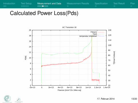
Calculated Power Loss(Pds)
0
2
4
6
8
10
12
14
16
18
20
-2e+13 0 2e+13 4e+13 6e+13 8e+13 1e+14 1.2e+14 1.4e+14 20
30
40
50
60
70
80
90
100
110
120
130
P[W
]
T[G
rad
Cel
sius
]
Fluence [n/cm^2/s 1Mev eq]
AC Transistor 18
Pds(y1)T(y2)
temperatur shutdown
17. Februar 2014 13/20

Introduction Test Setup Measurement and Data Measurement Results Specification Test Result Plan
Calculated Power Loss(Pds)
0
2
4
6
8
10
12
14
16
18
-5e+12 0 5e+12 1e+13 1.5e+13 2e+13 2.5e+13 3e+13 3.5e+13 4e+13 4.5e+13 20
30
40
50
60
70
80
90
100
110
120
P[W
]
T[G
rad
Cel
sius
]
Fluence [n/cm^2/s 1Mev eq]
AC Transistor 6
Pds(y1)T(y2)
temperatur shutdown
17. Februar 2014 14/20

Introduction Test Setup Measurement and Data Measurement Results Specification Test Result Plan
Calculated Ug saddle
0
0.5
1
1.5
2
2.5
3
3.5
-2e+13
0 2e+13
4e+13
6e+13
8e+13
1e+14
1.2e+14
1.4e+14
0
2e-07
4e-07
6e-07
8e-07
1e-06
1.2e-06
1.4e-06
1.6e-06
y1[V
]
y2[s
]
fluence
Ug Sattel Transistor 18 / Board: 5
Ug_sattel(y1)Tlen_sattel(y2)
17. Februar 2014 15/20

Introduction Test Setup Measurement and Data Measurement Results Specification Test Result Plan
Calculated Ug saddle
0
0.5
1
1.5
2
2.5
-5e+12
0 5e+12
1e+13
1.5e+13
2e+13
2.5e+13
3e+13
3.5e+13
4e+13
4.5e+13
0
5e-07
1e-06
1.5e-06
2e-06
2.5e-06
y1[V
]
y2[s
]
fluence
Ug Sattel Transistor 6 / Board: 2
Ug_sattel(y1)Tlen_sattel(y2)
17. Februar 2014 16/20

Introduction Test Setup Measurement and Data Measurement Results Specification Test Result Plan
Measurement Results
Main criteria for the acceptance is the point,when the Pds curveleave the lineary part.
Transistor Typ max NIELt24 SPA08N80C3 1.20E+14t22 FQPF9N90CT 1.15E+14t18 IXFH12N90P 7.90E+13t20 FQA11N90C 7.40E+13t26 STP6NK90ZFP 6.70E+13t28 IRFPE50 6.00E+13t16 IRFPE50 6.00E+13t14 IRFPF50 6.00E+13t4 STW13N95K3 3.286E+13t2 W12NK90Z 3.286E+13t30 SPW11N80C3 3.22E+13t8 STF6N95K5 2.626E+13t6 STW15NK90Z 2.596E+13t32 R8008ANX 2.50E+13t12 IPW90R500C3 2.50E+13t9 2SK3017(F) 2.20E+13
17. Februar 2014 17/20

Introduction Test Setup Measurement and Data Measurement Results Specification Test Result Plan
Radiation Environment Specification
Radiation Specification at the beginning of the upgrade project:Safety Factor
Per 100 fb−1 fb−1 fluence simulation simulation error low dose rate effects lot Specification FluenceTID [Gy] 0.43 10000 43 3.5 5 1 752.5NIEL [n/cm2] 3.00E+10 10000 3.00E+12 5 1 1 1.50E+13SEE [p/cm2] 3.70E+09 10000 3.70E+11 5 1 1 1.85E+12
Radiation Specification current version:Safety Factor
Per 100 fb−1 fb−1 fluence simulation simulation error low dose rate effects lot Specification FluenceTID [Gy] 0.43 3000 12.9 2 5 1 129NIEL [n/cm2]] 3.00E+10 3000 9.00E+11 2 1 1 1.80E+12SEE [p/cm2] 3.70E+09 3000 1.11E+11 2 1 1 2.22E+11
17. Februar 2014 18/20

Introduction Test Setup Measurement and Data Measurement Results Specification Test Result Plan
Test Result
For the new production of the DC/DC converter all Transistors aresuitable.
17. Februar 2014 19/20

Introduction Test Setup Measurement and Data Measurement Results Specification Test Result Plan
Next steps for the Power Mosfet test
Radiation Tests forTID - TestSEE - Test
17. Februar 2014 20/20


