The Electrodeposition of Gold by Pulse Plating IMPROVEMENTS IN THE PROPERTIES OF DEPOSITS Ch. J. Raub and A. Knödler Forschungsinstitut für Edelmetalle und Metallchemie, Schwäbisch Gmünd, West Germany The replacement of a direct by a pulsed current in the electrodeposition of gold has a marked effect in improving the mechanical properties of the deposits and in reducing their internal stresses. For many applications in the electronics industry pulse plating therefore offers considerable advantages. The use of pulsed current is well known as a research tool for studying the electrodeposition mechanism of metals. With increasing emphasis on the properties of the deposits, however, it was realised that this method of deposition could well provide a means of improving their properties. It was observed some years ago that either by periodically reversing the polarity of the current or by applying pulsed current, deposits of a much finer grain size could be obtained from cyanide (1) or from acid copper electrolytes (2, 3), and this has since been confirmed by other research workers for nearly all electroplated metals (3-10). The influence of pulsed current on the properties of chromium, for example, is espe- cially interesting, since its structure and properties, including internal stresses, are strongly influenced by the form of the applied current (11, 12, 13). It has also long been known that the structure and surface roughness of gold and gold alloy deposits can be influenced by periodically reversed or pulsed current, but this interest developed greatly when it was realised that pulse plated gold deposits proved superior to D.C. plated deposits for certain electronic applications, a discovery which was carefully followed up at Western Electric and from whence nearly all the information published on the industrial applica- tion of the pulse plating of gold has come. According to Avila and Brown (8) industrial pulse plating was first attempted at the Western Electric Engineering Research Center, Princeton, New Jersey, in June 1967. In the following year ap- parently the need for a high conductivity gold electrodeposit for integrated circuitry initiated the development of a pulse plating unit which supplied an on-off D.C. pulse with on- and off-times in the millisecond range and operated with current peaks up to 8 A. In general the on- and off-times were in the range of 1:10. The advantages claimed for the pulse plating of gold were: (1) A substantial increase in rate of deposition. (2) Less danger of hydrogen embrittlement. (3) A reduction in the need for additives. (4) A lower level of impurities from the electrolyte. Pulse plating of gold in the production of semi- conductor devices seems to be a procedure which is comparable to vacuum deposition but much more convenient and rapid, especially for experimental purposes (16). One of the direct industrial applications of pulse plating is the "beam-cross over plating" on a thin- film circuit. This technique enables the crossing of conductor paths on a thin-film circuit such as is shown in Figure 1. There can be as many as 2500 crossovers on a substrate. The dimensions of the Fig. 1 Sketch of a beam crossover. The number of crossovers on a substrate may vary up to 2500 38
Transcript
The Electrodeposition of Goldby Pulse PlatingIMPROVEMENTS IN THE PROPERTIES OF DEPOSITS
Ch. J. Raub and A. KnödlerForschungsinstitut für Edelmetalle und Metallchemie, Schwäbisch Gmünd, West Germany
The replacement of a direct by a pulsed current in the electrodepositionof gold has a marked effect in improving the mechanical propertiesof the deposits and in reducing their internal stresses. For manyapplications in the electronics industry pulse plating therefore offersconsiderable advantages.
The use of pulsed current is well known as aresearch tool for studying the electrodepositionmechanism of metals. With increasing emphasis onthe properties of the deposits, however, it was realisedthat this method of deposition could well provide ameans of improving their properties. It was observedsome years ago that either by periodically reversingthe polarity of the current or by applying pulsedcurrent, deposits of a much finer grain size could beobtained from cyanide (1) or from acid copperelectrolytes (2, 3), and this has since been confirmedby other research workers for nearly all electroplatedmetals (3-10). The influence of pulsed current onthe properties of chromium, for example, is espe-cially interesting, since its structure and properties,including internal stresses, are strongly influencedby the form of the applied current (11, 12, 13).
It has also long been known that the structure andsurface roughness of gold and gold alloy deposits canbe influenced by periodically reversed or pulsedcurrent, but this interest developed greatly when itwas realised that pulse plated gold deposits provedsuperior to D.C. plated deposits for certain electronicapplications, a discovery which was carefully followedup at Western Electric and from whence nearly allthe information published on the industrial applica-tion of the pulse plating of gold has come.
According to Avila and Brown (8) industrial pulseplating was first attempted at the Western ElectricEngineering Research Center, Princeton, NewJersey, in June 1967. In the following year ap-parently the need for a high conductivity goldelectrodeposit for integrated circuitry initiated thedevelopment of a pulse plating unit which suppliedan on-off D.C. pulse with on- and off-times in themillisecond range and operated with current peaks upto 8 A. In general the on- and off-times were in the
range of 1:10. The advantages claimed for the pulseplating of gold were:
(1) A substantial increase in rate of deposition.
(2) Less danger of hydrogen embrittlement.
(3) A reduction in the need for additives.
(4) A lower level of impurities from the electrolyte.
Pulse plating of gold in the production of semi-conductor devices seems to be a procedure which iscomparable to vacuum deposition but much moreconvenient and rapid, especially for experimentalpurposes (16).
One of the direct industrial applications of pulseplating is the "beam-cross over plating" on a thin-film circuit. This technique enables the crossing ofconductor paths on a thin-film circuit such as isshown in Figure 1. There can be as many as 2500crossovers on a substrate. The dimensions of the
Fig. 1 Sketch of a beam crossover. The number ofcrossovers on a substrate may vary up to 2500
38
:Fig. 2 Relationship between porosity and thicknessof various types of gold films according to Rehgig (15)
electron gun evaporation---_ - asymmetric A.C. plating
crossover are, for example 8 mil wide, 50 mil long,and of the pillars 3 X5 mil (14). It was quite aproblem to ensure good plating into the hole and toestablish good contact of the beam to the pillar. Byusing pulse plating this problem was solved. Also itwas possible to avoid unnecessary edge build-up(dog boning) of beam and lower conductor whichmight cause clearance and breakdown problems inthin film circuitry.
Among the advantages of pulse plating a higherrate of deposition is often included (8). By using forexample 8 to 10 A/ft2 pulsed current instead of4 to 5 A/ft2 Pcihoda and Walker (14) were able toreduce plating time by half. Cheh (17) has donetheoretical calculations and experimental measure-ments which clearly show that for phosphate, citrateand cyanide gold electrolytes the limiting currentdensity is higher in pulse than in D.C. plating becauseof the higher concentration of gold ions in the diffu-sion layer, although the limiting over-all plating rateis lower. According to Cheh this increase in thelimiting current density might be the reason for theimproved physical properties by yielding a differenttype of structure in the deposit.
Properties of the Deposits
resistivity of normal D.C. plated layers (8). The factthat pulse plated deposits have the lowest porosity ofall gold films deposited by various methods wasattributed by Rehrig (15) to the densely packed con-tinuous fine grained structure with barely visiblegrain boundaries. One of his graphs is shown inFigure 2. The very small grain size and the highpurity also serve to explain the difference in tensilestrength and elongation observed by Lendvay andRaub (6) and shown in Figure 3. In the as-depositedcondition fine-grained deposits gave a tensile strengthabout 25 per cent higher than with D.C. plateddeposits, while elongation increased by a factor of 2.D.C. plated deposits show a slight increase in tensilestrength after heat treatment at 100°C, which isfollowed by a continuous decrease at higher tem-peratures, while elongation rose more or less steadily.The increase at 100°C is very likely due to thebeginning of decomposition of incorporated im-purities. Pulse plated deposits with lower impurityconcentrations do not show any hardening effect. Asone might expect from a purer metal, its tensilestrength also decreases much more rapidly duringheating.
TEMPERATURE 'C
From the results of a number of investigations it isclear that pulse plating markedly affects the proper- Fig. 3 Tensile strength and elongation of pulsedties of the deposit. It was discovered in the early days current and direct current plated deposits from athat pulse plating of fine gold deposits produces a phosphate gold solution (20jum)dense fine-grained structure with about half the
39
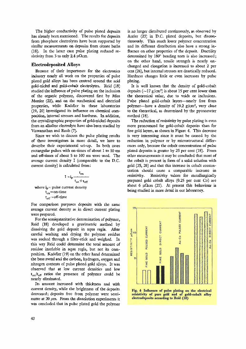
The higher conductivity of pulse plated depositshas already been mentioned. The results for depositsfrom phosphate electrolytes have been supported bysimilar measurements on deposits from citrate baths(18). In the latter case pulse plating reduced re-sistivity from 3 to only 2.4 µQcm.
Electrodeposited AlloysBecause of their importance for the electronics
industry nearly all work on the properties of pulseplated gold alloys has been centred around the acidgold-nickel and gold-cobalt electrolytes. Reid (18)studied the influence of pulse plating on the inclusionof the organic polymer, discovered first by MissMunier (22), and on the mechanical and electricalproperties, while Knödler in these laboratories(19, 20) investigated its influence on chemical com-position, internal stresses and hardness. In addition,the crystallographic properties of gold-nickel depositsfrom an alkaline electrolyte have also been studied byViswanathan and Raub (7).
Since we wish to discuss the pulse plating resultsof these investigators in more detail, we have todescribe their experimental set-up. In both casesrectangular pulses with on-times of about 1 to 10 msand off-times of about 5 to 100 ms were used. Theaverage current density I (comparable to the D.C.current density) is calculated from:
tonI = ip
ton+toff
where ip =pulse current densityt°n = on-timetoff=off-time
For comparison purposes deposits with the sameaverage current density as in direct current platingwere prepared.
For the semiquantitative determination of polymer,Reid (18) developed a gravimetric method bydissolving the gold deposit in aqua regia. Aftercareful washing and drying the polymer residuewas sucked through a filter-stick and weighed. Inthis way Reid could determine the total amount ofresidue insoluble in aqua regia, but not its com-position. Knödler (19) on the other hand determinedthe base metal and the carbon, hydrogen, oxygen andnitrogen contents of pulse plated gold alloys. It wasobserved that at low current densities and lowt0 /toff ratios the presence of polymer could benearly eliminated.
Its amount increased with thickness and withcurrent density, while the brightness of the depositsdecreased; deposits free from polymer were semi-matte at 20 Vm. From the dissolution experiments itwas concluded that in pulse plated gold the polymer
is no longer distributed continuously, as observed byAntler (23) in D.C. plated deposits, but discon-tinuously. This much lower polymer concentrationand its different distribution also have a strong in-fluence on other properties of the deposit. Ductilitydetermined by 180 ° bending tests is also increased;on the other hand, tensile strength is nearly un-changed and elongation is increased to about 2 percent (24), but internal stresses are drastically reduced.Hardness changes little or even increases by pulseplating.
It is well known that the density of gold-cobaltdeposits (-17 g/cm 3) is about 15 per cent lower thanthe theoretical value, due to voids or inclusions.Pulse plated gold-cobalt layers—nearly free frompolymer—have a density of 19.2 g/cm3, very closeto the theoretical, as determined by the pycnometermethod (18).
The reduction of resistivity by pulse plating is evenmore pronounced for gold-cobalt deposits than forfine gold layers, as shown in Figure 4. This decreaseis very interesting since it must be caused by thereduction in polymer or by microstructural differ-ences only, because the cobalt concentration of pulseplated deposits is greater by 25 per cent (18). Fromother measurements it may be concluded that most ofthe cobalt is present in form of a solid solution withgold (25, 26) and that this increase in cobalt concen-tration should cause a comparable increase inresistivity. Resistivity values for metallurgically
prepared gold cobalt alloys (0.25 per cent Co) areabout 6 µQcm (21). At present this behaviour isbeing studied in more detail in our laboratory.
5
W
zUi - u
z X -J üß: ä' U ä W
ü u 0V ^ W 0o , Q v
_5ö wz s `
W
H{1 IiFig. 4 Influence of pulse plating on the electricalreisistivity of pure gold and of gold-cobalt alloyelectrodeposits according to Reid (18)
E
a
I->
M
40
O SEMI-BRIGHT• MATTE
•/. N
n'+ ^r
I-wU
-̂-A - -- -A--6-
«
7 A/t1m2 0.5 g/l Ni, pH 3.5
U
1 A,4dm2 30.0 pH 3.5 r'0.8 - DIRECT CURRENT / a
0.3 - -- - PULSED CURRENT a •!.Co 600 BRIGHT
I-• MATTE /
W 0.6
ä g02 ^ 40
F_x 0.4
X. •/.Co i)LL
w ; I QAu'O wcrz .n'00.1 0 p^ 2O.j
O d
0.1 0,2 0.3 0.4 0.5COBALT S0
Fig.:5 Cobalt and carbon contents, and current effici-ency of direct current and of pulsed current platedgold-cobalt deposits as a function of cobalt concentra-tion of the electrolyte.
1 A/dma 30°C pH 3.5 9.--- DIRECT CURRENT
0.8 PULSED CURRENT /^0 BRIGHT / •/. NiO SEMI-BRIGHT cI
Fig. 6 Nickel and carbon contents, and current effici-envy of direct current and of pulsed current platedgold-nickel deposits as a function of nickel concentra-tion of the electrolyte
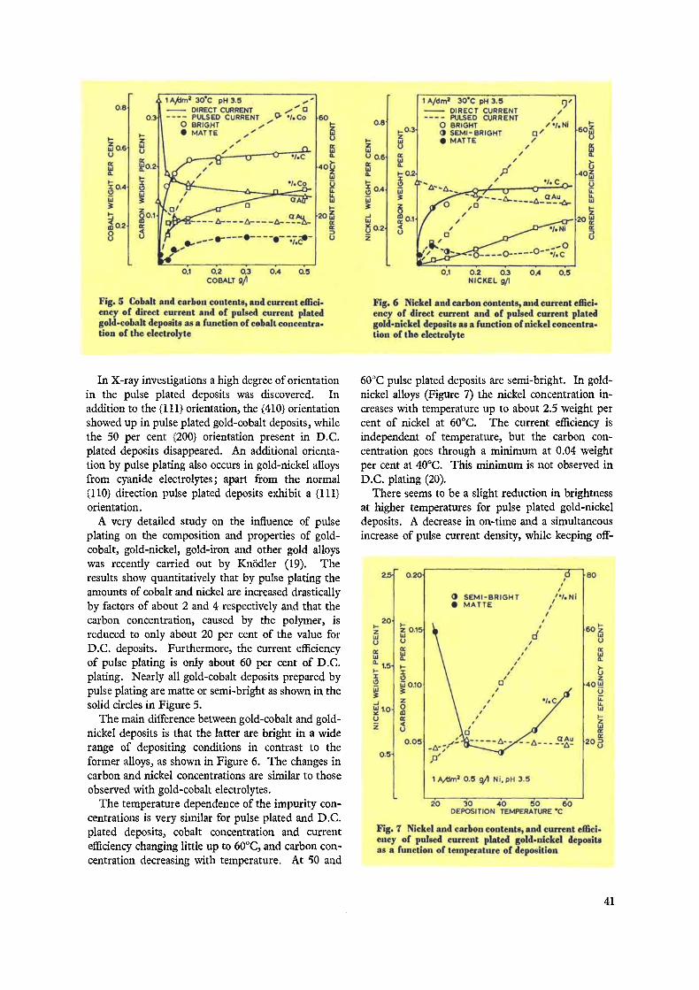
In X-ray investigations a high degree of orientationin the pulse plated deposits was discovered. Inaddition to the {111} orientation, the {410} orientationshowed up in pulse plated gold-cobalt deposits, whilethe 50 per cent (200) orientation present in D.C.plated deposits disappeared. An additional orienta-tion by pulse plating also occurs in gold-nickel alloysfrom cyanide electrolytes; apart from the normal(110) direction pulse plated deposits exhibit a (111)orientation.
A very detailed study on the influence of pulseplating on the composition and properties of gold-cobalt, gold-nickel, gold-iron and other gold alloyswas recently carried out by Knödler (19). Theresults show quantitatively that by pulse plating theamounts of cobalt and nickel are increased drasticallyby factors of about 2 and 4 respectively and that thecarbon concentration, caused by the polymer, isreduced to only about 20 per cent of the value forD.C. deposits. Furthermore, the current efficiencyof pulse plating is only about 60 per cent of D.C.plating. Nearly all gold-cobalt deposits prepared bypulse plating are matte or semi-bright as shown in thesolid circles in Figure 5.
The main difference between gold-cobalt and gold-nickel deposits is that the latter are bright in a widerange of depositing conditions in contrast to theformer alloys, as shown in Figure 6. The changes incarbon and nickel concentrations are similar to thoseobserved with gold-cobalt electrolytes.
The temperature dependence of the impurity con-centrations is very similar for pulse plated and D.C.plated deposits, cobalt concentration and currentefficiency changing little up to 60°C, and carbon con-centration decreasing with temperature. At 50 and
60°C pulse plated deposits are semi-bright. In gold-nickel alloys (Figure 7) the nickel concentration in-creases with temperature up to about 2.5 weight percent of nickel at 60°C. The current efficiency isindependent of temperature, but the carbon con-centration goes through a minimum at 0.04 weightper cent at 40°C. This minimum is not observed inD.C. plating (20).
There seems to be a slight reduction in brightnessat higher temperatures for pulse plated gold-nickeldeposits. A decrease in on-time and a simultaneousincrease of pulse current density, while keeping off-
DEPOSITION TEMPERATURE °C
Fig. 7 Nickel and carbon contents, and current efci-envy of pulsed current plated gold-nickel depositsas a function of temperature of deposition
`- z 0,w wo
W° 1,5I-.
2 w0.3 3J
Y1.0 0u
41
^- •l.Ni
1
F- z •
u U .M O.8 cc0.2 ofW w ia d ^i
W 1A/dm''0.25g/I Ni,pH 3.5; 30 ° C
OA ö O,1W m
•la C
aWa
t9W
iida0U
I-zWU
Wa
H
15W
z0m
U
•l. Co
1A/dm 2 0.25g/I Co,pH 3.5; 30`C
'4aAu
OFF-TIME —or
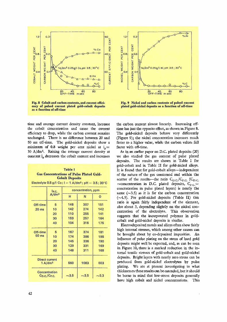
Fig. 8 Cobalt and carbon contents, and current effici-ency of pulsed current plated gold-cobalt depositsas a function of off-time
TIME m sec
Fig. 9 Nickel and carbon contents of pulsed currentplated gold-nickel deposits as a function of off-time
time and average current density constant, increasethe cobalt concentration and cause the currentefficiency to drop, while the carbon content remainsunchanged. There is no difference between 20 and50 ms off time. The gold-nickel deposits show aminimum of 0.8 weight per cent nickel at ip =30 A/dm2. Raising the average current density atconstant ip decreases the cobalt content and increases
the carbon content almost linearly. Increasing off-time has just the opposite effect, as shown in Figure 8.The gold-nickel deposits behave very differently(Figure 9); the nickel concentration increases muchfaster to a higher value, while the carbon values fallfaster with off time.
As in an earlier paper on D.C. plated deposits (20)we also studied the gas content of pulse plateddeposits. The results are shown in Table I forgold-cobalt and in Table II for gold-nickel alloys.It is found that for gold-cobalt alloys—independentof the nature of the gas concerned and within thescatter of the results—the ratio CD.C./Cp.C. (CD.C.=concentration in D.C. plated deposits, C p, c.=concentration in pulse plated layers) is nearly thesame (-3.5) as it is for the carbon concentration(-4.5). For gold-nickel deposits (Table II) thisratio is again fairly independent of the element,also about 3, depending slightly on the nickel con-centration of the electrolyte. This observationsuggests that the incorporated polymer in gold-cobalt and gold-nickel deposits is similar.
Electrodeposited metals and alloys often show fairlyhigh internal stresses, which among other causes canbe brought about by co-deposited impurities. Aninfluence of pulse plating on the stress of hard golddeposits might well be expected, and, as can be seenin Figure 10, there is a marked reduction in the in-ternal tensile stresses of gold-cobalt and gold-nickeldeposits. Bright layers with nearly zero stress can beproduced from gold-nickel electrolytes by pulseplating. We are at present investigating to whatthicknesses these results can be extended, but it shouldbe borne in mind that low-stress deposits generallyhave high cobalt and nickel concentrations. This
42
''o
^`^ Au-Ni Au-Co
Au-CÖ^ j
5SS
-
o---- u- --o•----- --=$
EEäY
NUi
U,W
zI-
shows that the stress in hard gold alloys is primarilycaused by the co-deposited non-metallic inclusionsand not by the base metal additions.
The hardness of pulse plated gold-cobalt depositsis about 10 per cent higher than that of comparableD.C. plated alloys. This is probably also due to thehigher base metal concentrations.
In reviewing the data on pulse plating it has to beborne in mind that three effects are unique:
(1)Due to the high current pulses high depositionpotentials are obtained which strongly favourthe co-deposition of the less noble metalscobalt and nickel.
(2)During off-times the depleted concentrationof metal ions in the cathodic layer can bereplenished by diffusion.
(3) During off-times, by-products formed duringthe cathodic discharge can diffuse out of thecathodic layer, thereby reducing their co-deposition.
Without going into details, we can thus explainthe fact that in pulse plating the decisive effects arethe restoring of the diffusion layer during off-timesby gold and cobalt complexes and the removal of by-products consisting of hydrogen, oxygen, carbonand nitrogen compounds from the cathode film.Without a knowledge of the diffusion coefficients ofthe various ions and/or radicals involved, moredetailed explanations have to remain somewhatspeculative. The pulse plating results stronglysupport the idea, however, that the co-depositedmaterial is mostly an organic compound, containingfairly little cobalt or gold. The influence of cobaltmay be a predominantly catalytic one. The earlier
I A/dm2 pH 3.5 ; 0.5 g/I Co or NtDIRECT CURRENT
-.--- PUUSED CURRENTO CI BRIGHTO.ü SEMI-BRIGHT• • MATTE
TION
Fig. 10 Tensile stress of direct current and pulsedcurrent plated gold cobalt and gold nickel deposits
observation that gold-nickel electrolytes behavedifferently has been confirmed.
Conclusions
This discussion of the literature and of our ownwork on the pulse plating of gold and gold alloys hasshown that it is possible to obtain deposits havingproperties which are superior to those of depositsobtained by normal D.C. plating. This methodalso makes possible the production of nearly stress-free deposits, while it also seems to furnish bettermicrothrowing power of the electrolytes.
Table 11
Gas Concentration of Gold-Nickel Deposits with Increasing Nickel Concentration of the ElectrolytepH 3.5, 30°C, lo,c. 1 A/dm 2, 1 10 A/nm 2, on time 2.6 ms, off-time 20 ms
:Nickelconcen- Concentration, ppm CD.C.0/P.C.
tratiön Currentg/l, H N 0 H N 0
0.1 D.C. 279 530 582 —2.2 N1.5 N2.0
P.G. 125 360 270
0.3 D.C. 343 865 485 N3.0 —2.5 —2.5
P.C. 122 353 201
0.5 D.G. 398 945 404 —5.0 s3.0 -3.0
P.C. 83 314. 1:38
43
Pulse plating is also especially valuable for in-vestigating the problem of polymer formation inhard gold deposits. It increases the amount of cobaltand nickel in the deposits drastically, and at the sametime reduces their contents of carbon, hydrogen,oxygen and nitrogen. With gold-nickel electrolytes,it is possible by pulse plating to produce brightdeposits with high nickel but low polymer con-centrations.
AcknowledgementsThe authors wish to express their gratitude to the
Chamber of Mines of South Africa for their support of thiswork.
References1 G. W. Jernstedt, Proc. Am. Electroplaters' Soc., 1949,
36, 63; 1950, 37, 1512 A. P. Popkov, J. Appl. Chem. U.S.S.R., 1966, 39, (8),
16323 A. M. Ozerov, N. P. Litvishko, I. N. Vavilina, P. M.
Chetvertnov and Ya. E. Zhak,,q. Appl. Chen. U.S.S.R.,1967, 40, (5), 1101
4 A. Hickling and H. P. Rothbaum, Trans. Inst. Met.Finish., 1957, 34, 199
5 C. C. Wan, H. Y. Cheh and H. B. Linford, Plating,1974, 61, (6), 559
6 J. Lendvay and Ch. J. Raub, Metalloberfläche, 1975, 29,(4), 165
7 M. Viswanathan and Ch. J. Raub, Surface Technol1976, 4, (4), 339
8 A. J. Avila and M. J. Brown, Plating, 1970, 57, (11),1105
9 M Viswanathan and Ch. J. Raub, Galvanotechnik,1975, 66, (4). 277
10 R. I. Gurovich and A. K. Krivtsov, Zh. Prikl. Khim.(Leningrad), 1968, 41, (6), 1227
11 C. L. Faust, G. R. Schaer and D. E. Semones, Plating,1961, 48, (6), 605
12 A. Knödler, Galvanotechnik, 1970, 61, (4), 29013 H. Schreiner and Ch. J. Raub, Z. Werkstofjtech., 1975,
6, (12), 41414 W. W. Pcihoda and A. E. Walker, Electron. Packag.
Prod., 1975, 15, (6), 7415 D. L. Rehrig, Plating. 1974, 61, (1), 4316 C. A. Burrus,,7. Electrochem. Soc., 1971, 118, (5), 83317 H. Y. Cheh,,J. Electrochem. Soc., 1971, 118, (4), 55118 F. H. Reid, Metalloberfidche, 1976, 30, (10), 45319 A. Knödler, Galvanotechnik, 1977, in the press20 A. Knödler, Metallober{idche, 1974, 28, (12), 46521 A. S. Darling, Gold Bull„ 1972, 5, (4), 7422 G. B. Munier, Plating, 1969, 56, (10), 115123 M. Antler, Plating, 1973, 60, (5), 46824 Ch. J. Raub, and J. Lendvay, unpublished results25 Ch. J. Raub, H. R. Khan and J. Lendvay, Gold Bull.,
1976, 9, (4), 12326 A. F. Mohrnheim, Y. Electrochem. Soc., 1970, 117, (6),
833
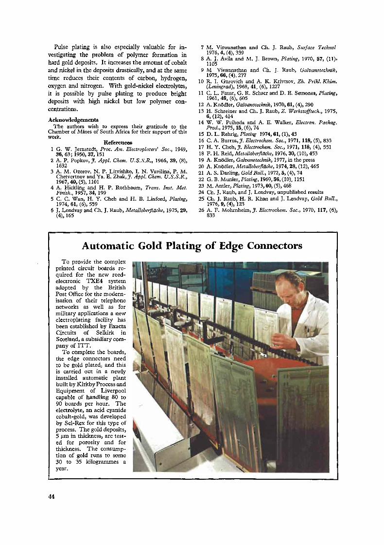
Automatic Gold Plating of Edge Connectors
To provide the complexprinted circuit boards re-quired for the new reed-electronic TXE4 systemadopted by the BritishPost Office for the modern-isation of their telephonenetworks as well as formilitary applications a newelectroplating facility hasbeen established by ExactaCircuits of Selkirk inScotland, a subsidiary com-pany of ITT.
To complete the boards,the edge connectors needto be gold plated; and thisis carried out in a newlyinstalled automatic plantbuilt by Kirkby Process andEquipment of Liverpoolcapable of handling 80 to90 boards per hour. Theelectrolyte, an acid cyanidecobalt-gold, was developedby Sel-Rex for this type ofprocess. The gold deposits,5 µm in thickness, are test-ed for porosity and forthickness. The consump-tion of gold runs to some30 to 35 kilogrammes ayear..