B.Tech 5 th Semester Examination December 2014 Microprocessor and interfacing (Paper EE-309-F) Time : 3 Hours MM: 100 Note: Attempt five questions in all, selecting at least one question from each unit. Q.no. 1 is compulsory. Q.1. (a) Differentiate between vectored and Non-Vectored interrupt. 4 (b) What is pipelining Flushing? How does this occur? 4 (c ) What are the advantages and disadvantages of memory mapped i/o over i/o mapped i/o. 4 (d) Explain the difference between segment and proc directives 4 (e) Explain Hidden DMA 4 UNIT-I 2. (a) Describe the PIN diagram of 8085 microprocessor. 10 (b) Write an ALP to find the number of negative numbers in the array. 10 3. (a) What is an interrupt? Explain the interrupt structure of 8085 microprocessor with suitable diagram. 10 (b) Write an ALP to transfer 150 bytes of data from memory location starting at 21000 to memory addressed by 31000h. 10 UNIT-II 4. (a) Explain EU and BIU of 8086 microprocessor 10 (b) What is pipelining? How is 8086 architecture designed to incorporate Pipelining? 10 5. (a) calculate the Physical address represented by: 10 (i) 1234h : 0002h (ii) F2F2h : 1234h (b) Describe the 8086 instruction Queue. Explain the advantages of Program relocation in 8086 microprocessor. 10
Transcript
B.Tech 5th Semester Examination December 2014
Microprocessor and interfacing (Paper EE-309-F)
Time : 3 Hours MM: 100
Note: Attempt five questions in all, selecting at least one question from each unit. Q.no. 1 is
compulsory.
Q.1. (a) Differentiate between vectored and Non-Vectored interrupt. 4
(b) What is pipelining Flushing? How does this occur? 4
(c ) What are the advantages and disadvantages of memory mapped i/o over i/o mapped
i/o. 4
(d) Explain the difference between segment and proc directives 4
(e) Explain Hidden DMA 4
UNIT-I
2. (a) Describe the PIN diagram of 8085 microprocessor. 10
(b) Write an ALP to find the number of negative numbers in the array. 10
3. (a) What is an interrupt? Explain the interrupt structure of 8085 microprocessor with suitable
diagram. 10
(b) Write an ALP to transfer 150 bytes of data from memory location starting at 21000 to
memory addressed by 31000h.
10
UNIT-II
4. (a) Explain EU and BIU of 8086 microprocessor 10
(b) What is pipelining? How is 8086 architecture designed to incorporate Pipelining? 10
5. (a) calculate the Physical address represented by:
10
(i) 1234h : 0002h
(ii) F2F2h : 1234h
(b) Describe the 8086 instruction Queue. Explain the advantages of Program relocation in
8086 microprocessor. 10
UNIT-III
6. (a) Explain directive and identifiers used in 8086 microprocessor.
10
(b) Write a simple ALP to add two memory locations where each memory location is one
byte wide. 10.
7. (a) Explain NOP and HLT instructions with the help of suitable example.
10
(b) Explain instruction execution timing with example. 10
UNIT-IV
8. (a) Describe the major components of 8279 keyboard / display interface with the help of its
block diagram 10
(b) List the Operating modes of 8255 PPI Chip. 10
9. (a) Explain the 8237 DMA controller with the help of PIN diagram
10
(b) Explain:
10
(i) Mode-2 strobed bidirection I/O of 8255
(ii) Priority Resolver
SOLUTION:
B.Tech 5th Semester Examination December 2014
Microprocessor and interfacing Paper EE-309-F
Time : 3 Hours MM: 100
Note: Attempt five questions in all, selecting at least one question from each unit. Q.no. 1 is
compulsory.
Q.1. (a) Differentiate between vectored and Non-Vectored interrupt. 4
Vector Interrupt: In this type of interrupt, Processor knows the address of Interrupt. In other
word processor knows the address of interrupt service routine. The example of vector interrupt
are RST 7.5, RST 6.5, RST 5.5, TRAP.
Non-Vector Interrupt: In this type of interrupt, Processor cannot know the address of Interrupt.
It should give externally. In the device will have to send the address of interrupt service routine
to processor for performing Interrupt. The example of Non-vector interrupt is INTR.
(b) What is pipelining Flushing? How does this occur? 4
Modern CPUs are pipelined, this means that instructions are executed in discrete "stages". Each
stage of the pipeline deals with a instruction, if the first instruction of the program has left the
instruction fetch stage, that stage might fetch another instruction, as soon as the first instruction
leaves the instruction decode stage, the instruction decode might fetch another instruction from
the instruction fetch stage and so on.
Problem is, if you have an instruction like jnz (or bnz) "jump if not zero" in the middle of the
instruction stream, it cannot be executed until all instructions that preceded it are completely
executed and the flag register is stabilized into a known state. This will cause the pipeline to
insert bubbles (effectively NOP instructions) until the pipeline is flush and the jnz can be
executed. If the CPU has a branch prediction unit, it will execute the JNZ regardless of the other
instructions and later check if the jump was correct.
(c ) What are the advantages / disadvantages of memory mapped i/o over i/o mapped i/o. 4
Advantages of I/O Mapped I/O Advantages of Memory Mapped I/O
Total 256 address space are available for I/O
devices
The memory mapped I/O scheme can provide
more than 256 I/O ports, as the port addresses
are 16-bits.
Program writing will be easy as special
instructions are used for I/O operations. In
8085 MPU, IN and OUT instructions are
usually used for data transfer with I/O devices
All memory related instructions can be used in
read /write operations of the memory mapped
I/O. The arithmetic and logical operations can
be performed on available I/O data directly
In I/O mapped I/O scheme, the I/O address
length is usually one byte and instructions are
two byte long. Therefore the program require
less memory and shorter execution time
compared to memory mapped I/O
CPU registers can exchange transfer of data
with I/O devices directly without accumulator
The memory reference instructions can be
easily distinguished from I/O reference
instructions, which make program debugging
easier
Memory mapped I/O simplifies and increases
speed of data transfer.
Disadvantages of I/O mapped I/O Disadvantages of memory mapped I/O
One MPU pin must be used to distinguish
between memory and I/O operations. The
additional control signals IOR and IOW must
be generated for read/write operations
Memory mapped I/O scheme utilizes memory
reference instructions, which are three byte
instructions and is longer than I/ instructions
In data transfer with I/O devices and MPU, the
data has to be transferred to ACC only to
perform arithmetic and logic operations.
Different addressing modes are not used in I/O
mapped I/O
Due to wider port addresses, the interface of
hardware is also complicated.
The complexity of the program is also large.
(d) Explain the difference between segment and proc directives 4
Sl SEGMENT DIRECTIVE PROC DIRECTIVE
1 The segment directive indicates the
beginning of a logical segment.
PROC directive is used to identify the start of
a procedure
2 Need The ASSUME directive to tell the
assembler that the name of the logical
segment should be used for a specified
segment.
No other directive is required
3 Does not need a call to SEGMENT Procedure is called by a CALL statement
4 Segment is ended by ENDS directive Procedure is ended by ENDP directive
5 Type of segment CS, DS, ES, SS are
mapped to the segment name by the
assume directive
The term near or far is used to specify the
type of the procedure
(e) Explain Hidden DMA 4
It is possible to perform hidden DMA, which is transparent to the normal operation of the CPU.
In other words, the bus is grabbed by the DMA controller when the processor is not using it. The
DMA controller monitors the execution of the processor, and when it recognises the processor
executing an instruction which has sufficient empty clock cycles to perform a byte transfer, it
waits till the processor is decoding the op code, then grabs the bus during this time. The
processor is not slowed down, but continues processing normally. Naturally, the data transfer by
the DMA controller must be completed before the processor starts
UNIT-I
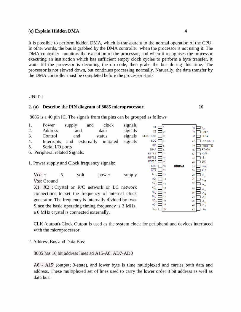
2. (a) Describe the PIN diagram of 8085 microprocessor. 10
8085 is a 40 pin IC, The signals from the pins can be grouped as follows
1. Power supply and clock signals
2. Address and data signals
3. Control and status signals
4. Interrupts and externally initiated signals
5. Serial I/O ports
6. Peripheral related Signals:
1. Power supply and Clock frequency signals:
Vcc: + 5 volt power supply
Vss: Ground
X1, X2 : Crystal or R/C network or LC network
connections to set the frequency of internal clock
generator. The frequency is internally divided by two.
Since the basic operating timing frequency is 3 MHz,
a 6 MHz crystal is connected externally.
CLK (output)-Clock Output is used as the system clock for peripheral and devices interfaced
with the microprocessor.
2. Address Bus and Data Bus:
8085 has 16 bit address lines ad A15-A8, AD7-AD0
A8 - A15: (output; 3-state), and lower byte is time multiplexed and carries both data and
address. These multiplexed set of lines used to carry the lower order 8 bit address as well as
data bus.
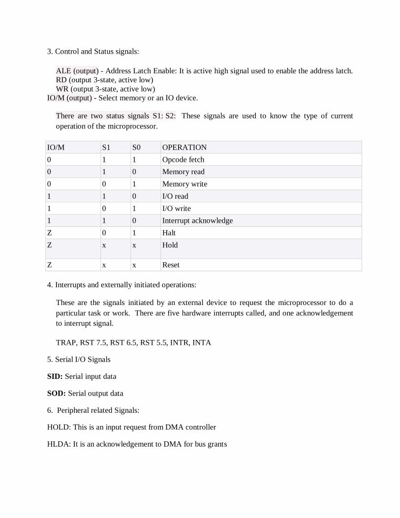
3. Control and Status signals:
ALE (output) - Address Latch Enable: It is active high signal used to enable the address latch.
RD (output 3-state, active low)
WR (output 3-state, active low)
IO/M (output) - Select memory or an IO device.
There are two status signals S1: S2: These signals are used to know the type of current
operation of the microprocessor.
IO/M S1 S0 OPERATION
0 1 1 Opcode fetch
0 1 0 Memory read
0 0 1 Memory write
1 1 0 I/O read
1 0 1 I/O write
1 1 0 Interrupt acknowledge
Z 0 1 Halt
Z x x Hold
Z x x Reset
4. Interrupts and externally initiated operations:
These are the signals initiated by an external device to request the microprocessor to do a
particular task or work. There are five hardware interrupts called, and one acknowledgement
to interrupt signal.
TRAP, RST 7.5, RST 6.5, RST 5.5, INTR, INTA
5. Serial I/O Signals
SID: Serial input data
SOD: Serial output data
6. Peripheral related Signals:
HOLD: This is an input request from DMA controller
HLDA: It is an acknowledgement to DMA for bus grants
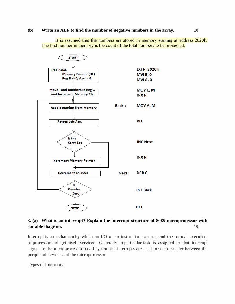
(b) Write an ALP to find the number of negative numbers in the array. 10
It is assumed that the numbers are stored in memory starting at address 2020h.
The first number in memory is the count of the total numbers to be processed.
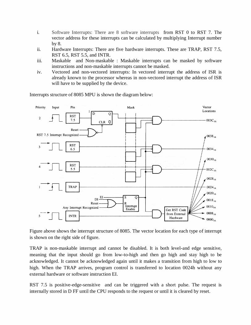
3. (a) What is an interrupt? Explain the interrupt structure of 8085 microprocessor with
suitable diagram. 10
Interrupt is a mechanism by which an I/O or an instruction can suspend the normal execution
of processor and get itself serviced. Generally, a particular task is assigned to that interrupt
signal. In the microprocessor based system the interrupts are used for data transfer between the
peripheral devices and the microprocessor.
Types of Interrupts:
i. Software Interrupts: There are 8 software interrupts from RST 0 to RST 7. The
vector address for these interrupts can be calculated by multiplying Interrupt number
by 8.
ii. Hardware Interrupts: There are five hardware interrupts. These are TRAP, RST 7.5,
RST 6.5, RST 5.5, and INTR.
iii. Maskable and Non-maskable : Maskable interrupts can be masked by software
instructions and non-maskable interrupts cannot be masked.
iv. Vectored and non-vectored interrupts: In vectored interrupt the address of ISR is
already known to the processor whereas in non-vectored interrupt the address of ISR
will have to be supplied by the device.
Interrupts structure of 8085 MPU is shown the diagram below:
Figure above shows the interrupt structure of 8085. The vector location for each type of interrupt
is shown on the right side of figure.
TRAP is non-maskable interrupt and cannot be disabled. It is both level-and edge sensitive,
meaning that the input should go from low-to-high and then go high and stay high to be
acknowledged. It cannot be acknowledged again until it makes a transition from high to low to
high. When the TRAP arrives, program control is transferred to location 0024h without any
external hardware or software instruction EI.
RST 7.5 is positive-edge-sensitive and can be triggered with a short pulse. The request is
internally stored in D FF until the CPU responds to the request or until it is cleared by reset.
RST 6.5 and RST 5.5: These interrupts are level-sensitive, meaning that the triggering level
should be ON until the CPU completes the execution o current instruction. If CPU is unable to
respond they should be stored internally or held by external hardware.
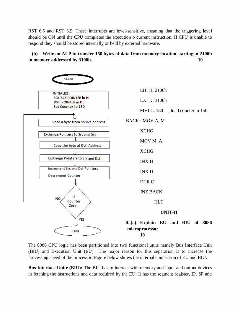
(b) Write an ALP to transfer 150 bytes of data from memory location starting at 2100h
to memory addressed by 3100h. 10
LHI H, 2100h
LXI D, 3100h
MVI C, 150 ; load counter to 150
BACK : MOV A, M
XCHG
MOV M, A
XCHG
INX H
INX D
DCR C
JNZ BACK
HLT
UNIT-II
4. (a) Explain EU and BIU of 8086
microprocessor
10
The 8086 CPU logic has been partitioned into two functional units namely Bus Interface Unit
(BIU) and Execution Unit (EU) The major reason for this separation is to increase the
processing speed of the processor. Figure below shows the internal connection of EU and BIU.
Bus Interface Unite (BIU): The BIU has to interact with memory and input and output devices
in fetching the instructions and data required by the EU. It has the segment register, IP, SP and
BP. It also incorporates an adder and multiply unit that calculates the physical address of the data
or instructions to be fetched from memory.
The functions performed by the Bus interface unit are:
- The BIU is responsible for the external bus operations.
- It performs fetching, reading, writing for memory as well as I/O of data for peripheral devices.
- The BIU also performs address generation and the population of the instruction queue.
Execution Unit: EU is responsible for executing the instructions of the programs and to carry
out the required processing. The main components in the EU are ALU, general purpose registers
and some special purpose registers as given below:
General purpose Registers: AX, BX, CX, DX
Index registers: SI, DI,
Pointer Registers: BP, SP
Flag Register with nine flags (OV, DF, TF, IF, S,Z,AC,P,Cy)
The Execution unit is responsible for the following work:
- The instructions are decoded and executed by it.
- The EU accepts instructions from the instruction queue and from the general purpose registers
it takes data.
- It has no relation with the system buses
(b) What is pipelining? How is 8086 architecture designed to incorporate Pipelining? 10
Instruction pipelining is a technique that implements a form of parallelism called instruction-
level parallelism within a single processor. It therefore allows faster CPU than would otherwise
be possible at a given clock rate. The basic instruction cycle is broken up into a series called
a pipeline. Rather than processing each instruction sequentially (finishing one instruction before
starting the next), each instruction is split up into a sequence of steps so different steps can be
executed in parallel and instructions can be processed concurrently (starting one instruction
before finishing the previous one).
This process is much faster than sending out an address, reading the opcode and then decoding
and executing it. In short fetching the next instruction while the current instruction is being
decoded or executed is called pipelining.
The 8086 architecture has a six-byte prefetch instruction pipeline and two separate units called
execution unit(EU) and bus interface unit (BIU). As the Execution Unit is executing the current
instruction, the bus interface unit reads up to six bytes of opcodes in advance from the memory.
The six byte long queue was chosen because the maximum number of bytes required for any
instruction in 8086 is this long.
The BIU is programmed to fetch a new instruction whenever the queue has room for one (with
the 8088) or two (with the 8086) additional bytes. The advantage of this pipelined architecture is
that the EU can execute instructions almost continually instead of having to wait for the BIU to
fetch a new instruction.
Pipelining increases instruction throughput by performing multiple operations at the same time,
but does not reduce instruction latency, which is the time to complete a single instruction from
start to finish, as it still must go through all steps. Indeed, it may increase latency due to
additional overhead from breaking the computation into separate steps and worse, the pipeline
may stall (or even need to be flushed), further increasing the latency.
Referring to the diagram, there are three conditions that will cause the EU to enter a "wait"
mode. These are:
i. The first occurs when an instruction requires access to a memory location not in the
queue. The BIU must suspend fetching instructions and output the address of this
memory location. After waiting for the memory access, the EU can resume executing
instruction codes from the queue (and the BIU can resume filling the queue).
ii. The second condition occurs when the instruction to be executed is a "jump"
instruction. In this case control is to be transferred to a new (non sequential) address.
The queue, however, assumes that instructions will always be executed in sequence
and thus will be holding the "wrong" instruction codes. The EU must wait while the
instruction at the jump address is fetched. Note that any bytes presently in the queue
must be discarded (they are overwritten).
iii. Third condition can cause the BIU to suspend fetching instructions. This occurs
during execution of instructions that are slow to execute. For example, the instruction
AAM (ASCII Adjust for Multiplication) requires 83 clock cycles to complete. At four
cycles per instruction fetch, the queue will be completely filled during the execution
of this single instruction. The BIU will thus have to wait for the EU to pull over one
or two bytes from the queue before resuming the fetch cycle.
A subtle advantage to the pipelined architecture should be mentioned. Because the next several
instructions are usually in the queue, the BIU can access memory at a somewhat "leisurely" pace.
This means that slow-memory parts can be used without affecting overall system performance.
5. (a) calculate the Physical address represented by: 10
(i) 1234h : 0002h
Solution:
Segment Value : 1234h
Base Address= Segment Value X 10h
= 1234h x 10h
= 12340h
Offset = 0002
Physical Address = Segment Value x 10h + Offset
= 12340h + 0002
= 12342h
(ii) F2F2h : 1234h
Solution:
Segment Value : F2F2h
Base Address= Segment Value X 10h
= F2F2h x 10h
= F2F20h
Offset = 0002
Physical Address = Segment Value x 10h + Offset
= F2F20h + 1234h
= F4174h
(b) Describe the 8086 instruction Queue. Explain the advantages of Program relocation
in 8086 microprocessor. 10
8086 has an instruction register which is a 6 byte first-in/first-out(FIFO) queue that is continually
filled whenever the system bus is not needed for some other operation. This “look ahead” feature
can significantly increase the CPU‟s throughput because much of the time the next instruction is
already in the CPU when the present instruction completes the execution. But if a branch type
instruction is being executed then the FIFO must be flushed out and in that case there is no time
saving, but on the average this occurs only for a small percent of time. For example, let us
consider the multiply instruction, it requires 71 clock cycles, but only 4 clock cycles are needed
to input a word from a memory. Therefore, during its execution there would be ample number of
extra clock cycles in which the bus is free to fill the instruction queue.
Program Relocation in 8086:
Any program in which the four segments are less than 64K in size are naturally relocatable or
position independent. This is because the physical address is formed using these segment
register. Any reference to an instruction or data byte is relative to one of the four segment
registers.
For example an instruction:
MOV num1, AX; refers to named location “num1” in the data segment area. When the OS
selects this program for execution, it loads the code and data are into any available memory
segment. Before the execution begins, the segment register can be set properly. Thus if the code
segment and data segment registers are set to 02000 and 04000 addresses, then when the
instruction MOV is executed, the data reference will automatically be relocated to address:
04000h + 0400h = 04400h.
While writing a program, it can be made re
locatable by avoiding addressing modes that result in absolute address, instead making use of the
aid of address register indirect address mode to refer to data operands. Thus address registers can
be loaded with the appropriate base address of data area
Advantage of Program Relocation:
i. It feature make the program free from the botheration of memory address conflicts.
ii. This feature will auto assign independent and separate address space the code and
data on which the instruction operates.
UNIT-III
6. (a) Explain directive and identifiers used in 8086 microprocessor. 10
Directives:
Just as high level language programs, 8086 also uses both the executable and non-executable
statements. The non-executable statements called directives are used to:
i. Preassign values
ii. Reserve storage
iii. Assign names to constants
iv. Form the data structures
v. Terminate a compilation
Because of the 8086‟s reliance on segment registers, 8086 assembler must also include directives
for indicating to the assembler the assumed contents in the segment registers under the various
circumstances as the assembly progresses.
Also as the assembly language is more close to the actual operations of the computer, most
assemblers have directives that give the programmer more control over the exact placement of
the data and segmentation of the program than is available to the high level language
programmer.
In general directives:
Provide information to the assembler while translating a program
Used to define data, select memory model, etc.
Non-executable: directives are not part of instruction set
Identifiers:
Identifiers are the character sequences which have a special, symbolic meaning to the assembler.
All identifiers in ASM-86 must obey the following rules:
i. The first character must be alphabet (A,….Z, a,………….,z)
ii. Any subsequent character can be either alphabetical or a numeral(0,1,……,9). ASM-
86 ignores the special characters @ and _, but they are still legal. For example, a_b
becomes ab.
iii. Identifiers may be of any length upto the limit of the physical line.
Identifiers are of two types:
a. Keywords: Keywords are those identifiers, which have predefined meaning to the
assembler and must not be used by the user for symbols(user defined identifiers like
variable, constants etc.)
b. Symbols: Symbols are the identifiers, which are defined by the user and may be used as
variables, labels, numbers.
The following are all valid identifiers:
NOLIST
WORD
AH
My_name
How_are_you
variable@number
The following are invalid:
123
12name
My name
@num1
1-247 characters, including digits
not case sensitive
first character must be a letter, _, @, ?, or $
(b) Write a simple ALP to add two memory locations where each memory location is
one byte wide. 10.
Solution: 8086 uses the memory segmentation, wherein the data part is stored in data
segment and the code is in code segment. The ALP is given below:
.model small
Data segment
Num1 db 25h
Num2 db 38h
Result db ?
Data ends
Code segment
ASSUME CS: code, DS, data
MOV AX, data
MOVE DS, AX
MOV AL, Num1
ADD AL, Num2
MOV resut, AL
code ENDS
END
7. (a) Explain NOP and HLT instructions with the help of suitable example. 10
An instruction that is quite often used in conjunction with branch instruction is the NOP (no
operation) instruction. The NOP instruction serve the same purpose as the CONTINUE
instruction in high level language, as a means of providing a label for a “bench to” point that
does nothing.
The availability of such an instruction is very important, particularly during the development of a
program, when modifications are frequently necessary. To attach the “branch to” label to an
instruction that takes action as follows:
JZ EXIT
- -
EXIT : MOV AX, SUM[BX]
Is relatively inflexible because, in order to insert new instruction at the point
labeled EXIT, the move instruction must be retyped.
JZ EXIT
---
EXIT : NOP
MOV AX, SUM[BX]
If the sequence given above was used, insertion could be made without disturbing
the present code. This is important during the debugging phase when message
printout code may need to be temporarily included at key points within a program.
HLT instruction: The HLT instruction causes the computer to cease its operation. By examining
the state of the CPU at the time it is halted one can get information regarding the recent activity
within the computer. HLT instruction are frequently found in diagnostic programs that are
designed to help maintain a computer system.
name Mnemonic and Forma Description
No Operation NOP Cause no action
Halt HLT Cause the operation of the
computer to cease.
(b) Explain instruction execution timing with example. 10
The execution time of an instruction can be determined by multiplying the number of clock
cycles needed to execute the instruction by the clock‟s period. It can be expressed as the sum of a
basic execution time (which varies depending on the instruction and addressing mode) plus the
time required to calculate the effective address if a memory operand is involved.
The basic execution time assumes that the instruction to be executed has already been
prefatched and stored in the instruction queue; otherwise, any additional clock cycles necessary
to fetch the instruction must be added.
For example:
Instruction Addressing
Mode
Example No. of clck
cycles
No. of transfers
ADD Reg-to-Reg ADD AL, BL 3 0
Mem-to-Reg ADD AL, [BX] 9+EA 1
Reg-to-Mem ADD [BX], AL 16+EA 2
Imm-to-Reg ADD AL, 55h 4 0
Imm-to-Mem ADD [BX], 55h 17+EA 2
Table above shows that some instruction have several different basic execution times depending
on the addressing mode.
To calculate the Execution Time:
For example, if clock has a frequency of 5MHz then the exection time for various forms of the
add instruction can be computed as:
Clock Period = 1/fc = 1/5MHz = 0.2 micro sec.
No. of clock cycles required
for byte or word operand
Time
ADD Reg-to-Reg
3 0.2x3=0.6 u sec
ADD Mem-to-Reg 9 + 12(for Addr. Calculation)
= 21 cycles for words at even
address
If word is at odd address then
4 addition clock cycles will
be required thus
Total clock= 9+12+4=25
0.2x21= 4.2 u sec
0.2x 25 = 5.0 u sec
UNIT-IV
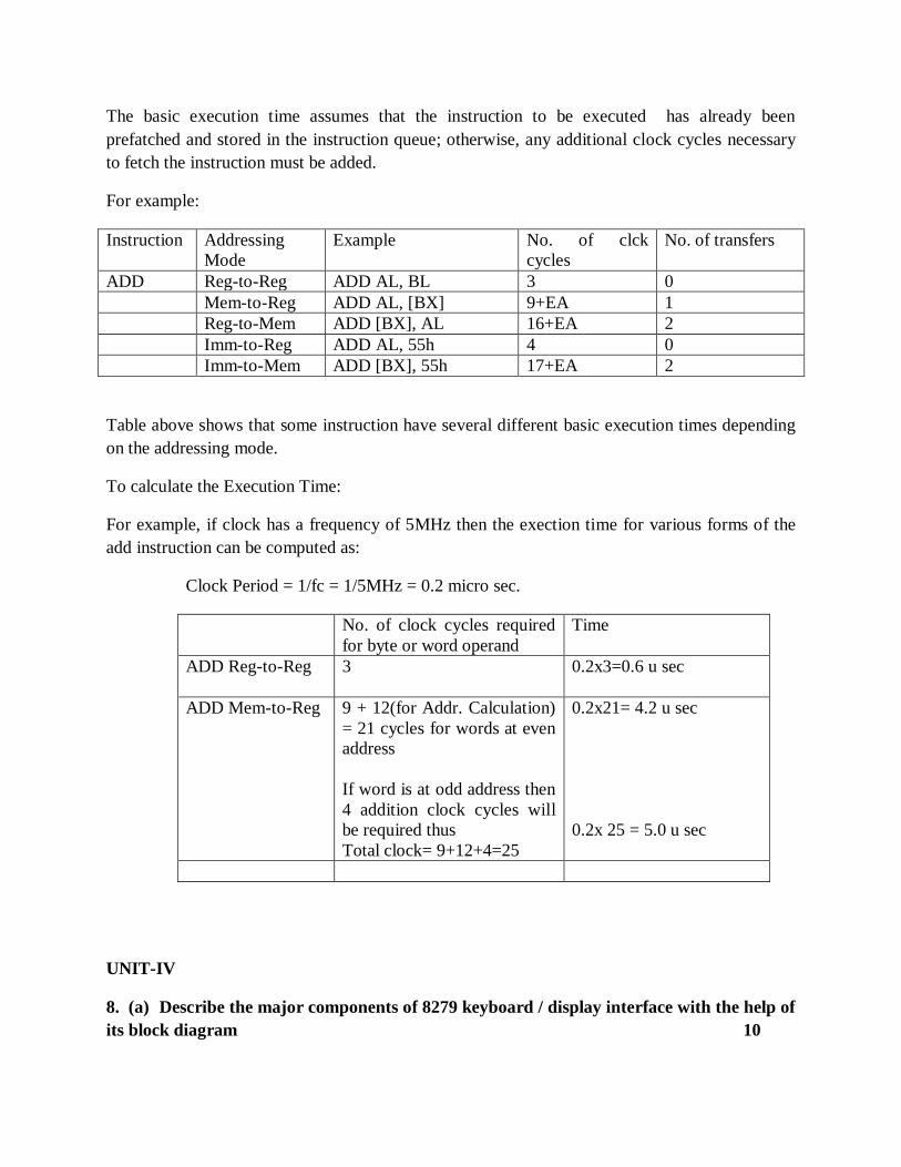
8. (a) Describe the major components of 8279 keyboard / display interface with the help of
its block diagram 10
Intel‟s 8279 is a general purpose Keyboard Display controller that simultaneously drives the
display of a system and interfaces a Keyboard with the CPU. The Keyboard Display interface
scans the Keyboard to identify if any key has been pressed and sends the code of the pressed key
to the CPU. It also transmits the data received from the CPU,
to the display device.
Both of these functions are performed by the controller in repetitive fashion without involving
the CPU. The Keyboard is interfaced either in the interrupt or the polled mode.In the interrupt
mode, the processor is requested service only if any key is pressed, otherwise the CPU can
proceed with its main task.
The pin Ao, RD and WR select the command, status or data read/write operations carried out by
the CPU with 8279.
Control and Timing Register and Timing Control
These registers store the keyboard and display modes and other operating conditions
programmed by CPU. The registers are written with A0=1 and WR =0. The timing and control
unit controls the basic timings for the operation of the circuit. Scan Counter divide down the
operating frequency of 8279 to derive scan keyboard and scan display frequencies.
Scan Counter
The Scan Counter has two modes to scan the key matrix and refresh the display. In the Encoded
mode, the counter provides a binary count that is to be externally decoded to provide the scan
lines for keyboard and display (four externally decoded scan lines may drive up to 16 displays).
In the decoded scan mode, the counter internally decodes the least significant 2 bits and provides
a decoded 1 out of 4 scan on SL0-SL3 (four internally decoded scan lines may drive up to 4
Displays). The Keyboard and Display both are in the same mode at a time.
Return Buffers and Keyboard Debounce and Control
This section scans for a Key closure row-wise. If it is detected, the Keyboard debounce unit
debounces the key entry (i.e. wait for 10 ms). After the debounce period, if the key continues to
be detected. The code of the Key is directly transferred to the sensor RAM along with SHIFT
and CONTROL key status.
FIFO/Sensor RAM and Status Logic
In Keyboard or strobed input mode, this block acts as 8-byte first-in-first-out (FIFO) RAM. Each
key code of the pressed key is entered in the order of the entry, and in the meantime, read by the
CPU, till the RAM becomes empty. The status logic generates an interrupt request after each
FIFO read operation till the FIFO is empty.
In scanned sensor matrix mode, this unit acts as sensor RAM. Each row of the sensor RAM is
loaded with the status of the corresponding row of sensors in the matrix. If a sensor changes its
state, the IRQ line goes high to interrupt the CPU.
Display Address Registers and Display RAM.
The Display address registers hold the addresses of the word currently being written or read by
the CPU to or from the display RAM. The contents of the registers are automatically updated by
8279 to accept the next data entry by CPU. The 16-byte display RAM contains the 16-byte of
data to be displayed on the sixteen 7-seg displays in the
encoded scan mode.
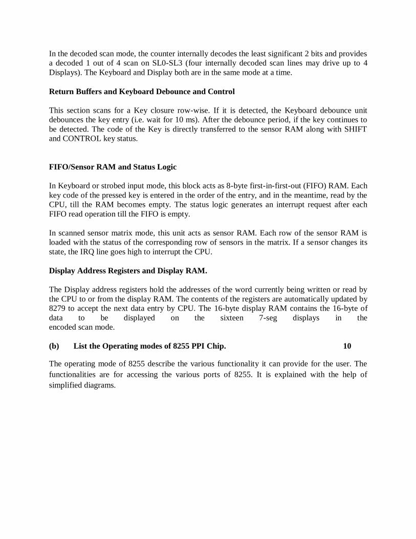
(b) List the Operating modes of 8255 PPI Chip. 10
The operating mode of 8255 describe the various functionality it can provide for the user. The
functionalities are for accessing the various ports of 8255. It is explained with the help of
simplified diagrams.
As seen in thediagram, the different operating modes are:
1. Bit Set/Reset (BSR) Mode
2. Input/Output (I/O) Mode: This mode is further of following types
i. Mode-0
ii. Mode-1
iii. Mode-2
These Modes are describe below:
1. Bit Set/Reset (BSR) Mode of Operation : BSR mode is used for Port-C to control read/write
operation on individual pins of port C. The control word of the BSR mode is shown in figure.
1. IO Mode of Operation : The IO mode is used for reading and writing from or to IO device. The
read write operations to/from IO devices can be performed in different modes. The control word
setting for the IO mode is shown in figure.
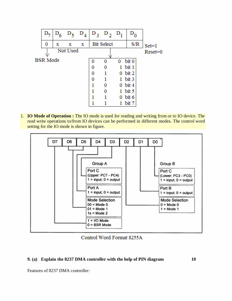
9. (a) Explain the 8237 DMA controller with the help of PIN diagram 10
Features of 8237 DMA controller:
i. It is housed in 40 pin DIP package.
ii. 8237 has 4 independent channel
iii. Each of the four channels are capable of
transferring 64Kbyte.
iv. It is an interface between the peripheral
and the microprocessor.
v. 8237 itself is an i/o device to the
microprocessor when used as slave.
vi. 8237 becomes bus controller or IOP
when used as master.
DMA signals are divided into two groups:
(a) Those required to communicate with
microprocessor, they are CS‟, A7-A0, DB7-
DB0, ADSTB, AEN, MEMR‟, MEMW‟, IOR‟,
IOW‟, READY, RESET, CLK, HRQ, HLDA
(b) Those required for communicating with the
peripherals they are DREQ3-DREQ0, DACK3-
DACK0 and EOP.
These signals are explained below:
DREQ3-DREQ0: One DREQ line for each channel. These are the request lines from the
peripherals such as floppy disk, hard disk etc. To obtain the DMA service, DMA request is
generated by the peripheral by activating the DREQ lines of the channel.
DACK3-DACK0: This is an acknowledgement from the DMA in response to the DREQ signal
from peripheral.
AEN and ADSTB: These are active high signals used to latch a high order address byte on the
data bus to generate 16-bit address.
A7-4 and A3-0: A3-0 are bidirectional lines and when DMA is slave these are inputs for
accessing the control registers and during DMA (master) cycle are used as output lines to
generate low-order address and combined with the remaining A7-A4 lines.
HRQ and HLDA: HRQ is a request line from the DMA controller to the processor for gaining
the control of the buses. And HLDA is the acknowledgement to the DMA controller in response
to the HRQ.
CS‟ : This is a chip select signal. It is only after the 8237 is selected can it be communicate with
the I/O and processor.
RESET: A high active signal on this line resets the command, status register, request and
temporary register. This maker the 8237 to enter the idle mode.
READY: Used to accommodate the slow operating memory or I/o devices by extending the
memory read/write inputs from 8237A.
DB7-DB0: these are the bata bus lines used to send command and information to/from the
processor and 8237.
IOR‟,IOW‟ MEMR‟,MEMW‟: control signals for I/O, and Memory read write operations.
EOP‟: This is an active low bidirectional signal and used to indicate completion of DMA service.
Also a low input on this line may be used to terminate the DMA operation.
(b) Explain: 10
(i) Mode-2 strobed bidirection I/O of 8255
8255A, Mode-2 operation allow bidirectional communication on port A with its
handshake signal on 5 pins of port C, port B can be used either in Mode-0 or Mode-1.
This mode is normally used for communication between two CPUs in which case one
of the CPU acts as master and the other is slave CPU.
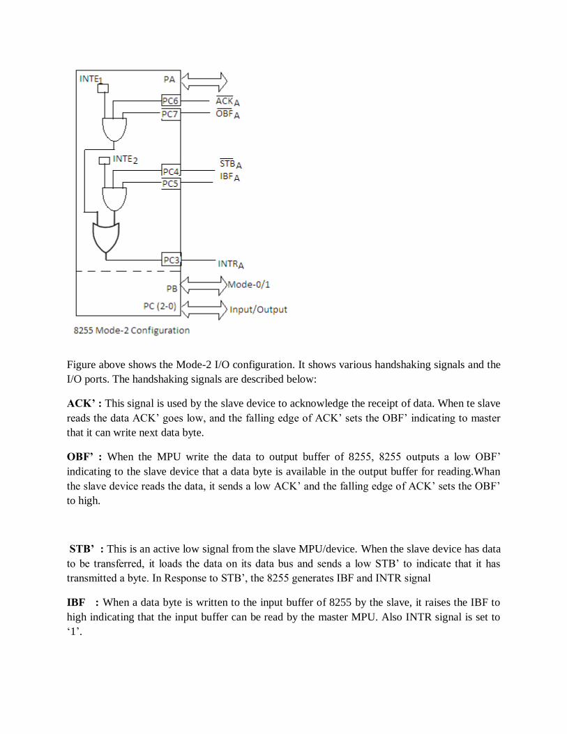
Figure above shows the Mode-2 I/O configuration. It shows various handshaking signals and the
I/O ports. The handshaking signals are described below:
ACK’ : This signal is used by the slave device to acknowledge the receipt of data. When te slave
reads the data ACK‟ goes low, and the falling edge of ACK‟ sets the OBF‟ indicating to master
that it can write next data byte.
OBF’ : When the MPU write the data to output buffer of 8255, 8255 outputs a low OBF‟
indicating to the slave device that a data byte is available in the output buffer for reading.Whan
the slave device reads the data, it sends a low ACK‟ and the falling edge of ACK‟ sets the OBF‟
to high.
STB’ : This is an active low signal from the slave MPU/device. When the slave device has data
to be transferred, it loads the data on its data bus and sends a low STB‟ to indicate that it has
transmitted a byte. In Response to STB‟, the 8255 generates IBF and INTR signal
IBF : When a data byte is written to the input buffer of 8255 by the slave, it raises the IBF to
high indicating that the input buffer can be read by the master MPU. Also INTR signal is set to
„1‟.
INTR: As seen in the figure there are two internal Flip-flops INTEA and INTEB which when set
can be used to generate INTR signal for interrupt driven I/O for a read or write operation.
(ii) Priority Resolver
Priority Resolver : This unit determines the priorities of the interrupt requests appearing simultaneously.
The highest priority is selected and stored into the corresponding bit of ISR during INTA pulse. The IR 0
has the highest priority while the IR 7 has the lowest one, normally in fixed priority mode. The priorities
however may be altered by programming the 8259A in rotating priority mode.
As an example of how this works, suppose that IR2 and IR4 are unmasked and that an interrupt signal
comes in on the IR4 input. The interrupt request on the IR4 input will set bit 4 in the interrupt request
register (IRR). The priority resolver will detect that this bit is set and check the bit in the in-service
register (ISR) to see if a high priority input is being serviced.
If a high priority input is being serviced, as indicated by the bit being set for that input in the ISR, then
the priority resolver will take no action. If no higher priority interrupt is being serviced, then the priority
resolver will activate the circuitary which sends an interrupt signal to the 8086.
When the 8086 responds with the INTA’ pulses, the 8259 will send the interrupt type that was specified
for the IR4 input when the 8259A was initialized. 8086 will use the type number it receives from 8259A
to find and execute the interrupt-service procedure written for the IR4 interrupt.
Now suppose that while 8086 is executing the IR4 service procedure, an interrupt signal arrives at IR2
input of 8259A. This will set bit 2 of IRR. Since we assumed for this example that IR2 was unmasked,
priority resolver will detect that this bit in the IRR is set and make a decision whether to send another
interrupt signal to the 8086. To make the decision, the priority resolver looks at the ISR. If a higher-
priority bit in the ISR is set, then a higher-priority bit in the ISR is set, then a higher-priority interrupt is
being serviced. The priority resolver will wait until the higher-priority bit in the ISR is reset before
sending an interrupt signal to 8086 for new interrupt input. If the priority resolver finds that the new
interrupt has higher priority has higher priority than the highest—priority interrupt currently being
service, it will set the appropriate bit in the ISR and activate the circuitary which sends a new INTR signal
to 8086. If the INTR input was enabled with the STI instruction at the start of the IR4 service procedure
then the new INT signal will interrupt the 8086 again. When the 8086 sends out a second INTA’ pulse in
respond to this interrupt, the 8259A will send it the type number for IR2 service procedure. The 8086
will use the received type number to find and execute the IR2 service procedure.
At the end of the IR2 procedure, we send the 8259A a command word that resets bit 2 of the ISR so that
lower-priority interrupt can be serviced. After that the IRET instruction at the end of IR2 procedure
sends execution back to the interrupted IR4 procedure. At the end of IR4 procedure, we send the 8259A
a command word which resets bit 4 of ISR so that lower-priority interrupts can be serviced. An IRET
instruction at the end of IR4 procedure returns execution to the main program
It consist of priority logic circuit which resolves the priority of each channel. The priority of
these channels may be fixed (by default priority) or as rotating priority. The priority can be set by
using the mode set register.
Mode Set Register:
When set, the various bits in the mode set register enable each of the four DMA channels, and
allows each of the four different options for the 8237/8257.
D7 D6 D5 D4 D3 D2 D1 D0
AL TCS EW RP EN3 EN2 EN1 EN0
EN0: Enable Channel 0 EN1: Enable Channel 1
EN2: Enable Channel 2 EN3: Enable Channel 3
RP: Rotating Priority EW: Extended write mode
TCS: Stop after TC AL: Auto Load mode
It is a write only register. It is used to set operating mode of 8237/8257. The mode set register is
programmed by the MPU after the DMA address register(s) and terminal count register(s) are
initialized. The mode set register is cleared by the reset input. When the register is cleared all the
operating modes and channels of 8257 are disabled, preventing bus conflicts on power up. A
channel should not be left enabled unless it DMA address and terminal count register contain
valid values; otherwise, an inadvertent DMA request(DRQn) from a peripheral could initiate a
DMA cycle that would destroy memory data.
The various operating modes, which are enabled by D4,D5,D6,D7 bits of the mode set register
are explained below:
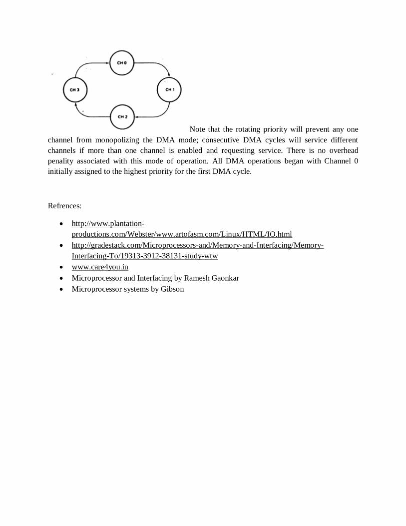
Rotating Priority:
In default mode 8237/8257 operates in fixed priority mode,CH0 having the highest priority and
CH3 having the lowest priority. The priority of the channels can be changed to rotating priority
by setting the bit D4 bit of the mode set register. In the rotating priority mode, the priority of the
channels has a circular sequence. After each DMA cycle, the priority of each channel changes.
The channel which has just been serviced has the lowest priority.
Note that the rotating priority will prevent any one
channel from monopolizing the DMA mode; consecutive DMA cycles will service different
channels if more than one channel is enabled and requesting service. There is no overhead
penality associated with this mode of operation. All DMA operations began with Channel 0
initially assigned to the highest priority for the first DMA cycle.