46
The CMOS Inverter Lecture 3a Static properties (VTC and noise margins)

The CMOS Inverter
Lecture 3a
Static properties
(VTC and noise margins)
Inputs
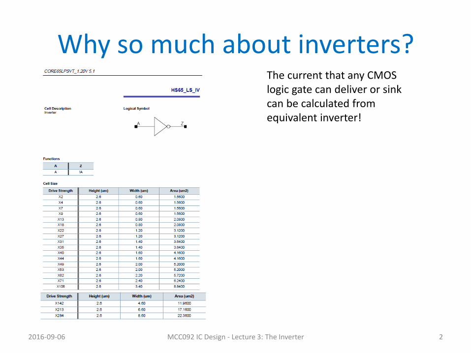
Why so much about inverters?
2016-09-06 MCC092 IC Design - Lecture 3: The Inverter 2
VDD
VSS
Y
nMOS pull-down network
pMOS pull-up
network IDSP
IDSN
The current that any CMOS logic gate can deliver or sink can be calculated from equivalent inverter!

Important CMOS Inverter knowledge
• First of all, of course the MOSFET schematic • But you will capture the inverter schematic in lab 1
MCC092 IC Design - Lecture 3: The Inverter 3
vdd!
gnd!
vdd!
2016-09-06
Don´t forget to tie the body to VDD and GND!
gnd!

The voltage characteristic (VTC) • VTC shows VOUT vs VIN in steady-state, i.e. quasi-static DC with
dVIN/dt=dVOUT /dt≈0!
MCC092 IC Design - Lecture 3: The Inverter 4
VIN
VOUT
PMOS
NMOS
• However, the PMOS has its ”origo” in (VDD, VDD) when connected to VDD as in the inverter
2016-09-06
VDD
VDD • NMOS works for positive gate and drain voltages
• PMOS works for negative gate and drain voltages

The voltage characteristic (VTC)
First task: to calculate the switching voltage VSW, i.e the input voltage that separates a ”one” and a ”zero”:
MCC092 IC Design - Lecture 3: The Inverter 5
VDD VSW VTN VDD+VTP 0 0
(VDD, VDD)
2016-09-06
Switching occurs in the green region where both MOSFETs are saturated!
1
NDD TP TN
P
sw
N
P
kV V V
kV
k
k
VDD
2 2
2 2
N PIN TN DD IN TP
k kV V V V V
Hence, let IDSN=ISDP
VOUT
VIN
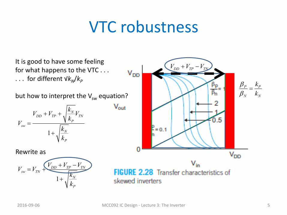
VTC robustness
MCC092 IC Design - Lecture 3: The Inverter 5
It is good to have some feeling for what happens to the VTC . . . . . . for different √kN/kP
but how to interpret the Vsw equation?
P P
N N
k
k
Rewrite as
1
DD TP TNsw TN
N
P
V V VV V
k
k
1
NDD TP TN
P
sw
N
P
kV V V
kV
k
k
DD TP TNV V V
2016-09-06

The voltage characteristic (VTC)
MCC092 IC Design - Lecture 3: The Inverter
VDD VSW
What if we make n-channel MOSFET wider?
What happens to VTC? VDD
VTN VDD+VTP 0 0
2016-09-06 7
Decreases, see slide 5!
1
DD TP TN
N P
V V V
k k
DD TP TNV V V
VSW increases or decreases?
VOUT
VIN

The voltage characteristic (VTC)
MCC092 IC Design - Lecture 3: The Inverter
VDD
VOUT
VSW
Which VTC is NAND and which VTC is NOR?
VDD
VTN VDD+VTP 0 0
2016-09-06 8
VIN
NAND
NOR

The voltage characteristic (VTC)
MCC092 IC Design - Lecture 3: The Inverter
VDD VSW
Find VTC equations for blue regions where only one MOSFET is saturated!
VDD
VTN VDD+VTP 0 0
2 2N
OUT IN TP IN TN DD IN TP
P
kV V V V V V V V
k
2016-09-06 9
Only n-channel MOSFET saturated
p-channel MOSFET saturated
2 2P
OUT IN TN IN TN DD IN TP
N
kV V V V V V V V
k
OUT IN TPV V V
OUT IN TNV V V
Saturation conditions
VOUT
VIN

The voltage characteristic (VTC)
MCC092 IC Design - Lecture 3: The Inverter
VDD VSW
How about current flow?
No current flow in red regions!
”short-circuit” current ISC flows in blue/green regions
VDD
VTN VDD+VTP 0 0
2016-09-06 10
2
2
NSC IN TN
kI V V
2
2
PSC DD IN TP
kI V V V
n-channel MOSFET saturated
p-channel MOSFET saturated
VOUT
VIN
Valid ”0”
Valid ”1”
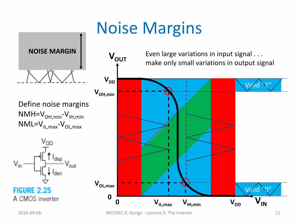
Noise Margins
2016-09-06 MCC092 IC Design - Lecture 3: The Inverter 11
VDD
VDD
0 0
VOH,min
VOL,max
VIH,min VIL,max
Even large variations in input signal . . . make only small variations in output signal
VIN
VOUT
Define noise margins NMH=VOH,min-VIH,min
NML=VIL,max-VOL,max
NOISE MARGIN
Valid ”0”
Valid ”1”
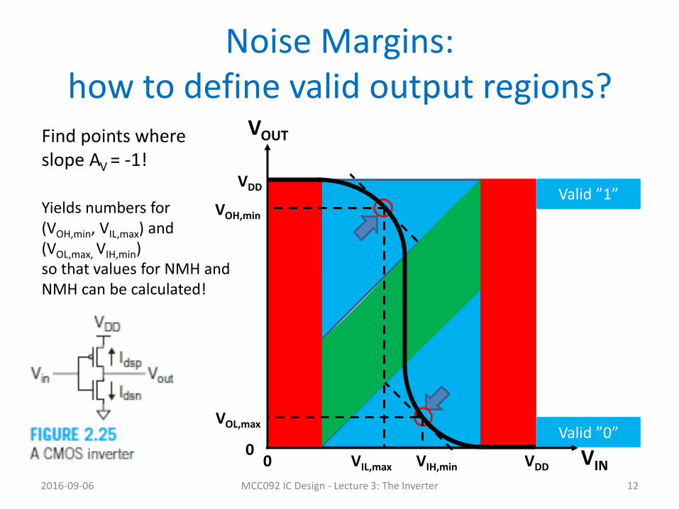
Noise Margins: how to define valid output regions?
2016-09-06 MCC092 IC Design - Lecture 3: The Inverter 12
VIN VDD
VOUT
VDD
0 0
Find points where slope AV = -1!
VIL,max VIH,min
Yields numbers for (VOH,min, VIL,max) and (VOL,max, VIH,min) so that values for NMH and NMH can be calculated!
VOH,min
VOL,max

Valid ”0”
Valid ”1”
Noise Margins – an example
2016-09-06 MCC092 IC Design - Lecture 3: The Inverter 13
VIN
VOUT
0 0
Find points where slope AV = -1!
1.2 V
1.06 V
0.12 V
1.2 V
0.7 V 0.5 V
Yields numbers for (VOH,min, VIL,max)=(1.06, 0.5) (VOL,max, VIH,min)=(0.12, 0.7) Hence NMH=1.06 – 0.7 = 0.36 V NML= 0.5 – 0.12 = 0.38 V
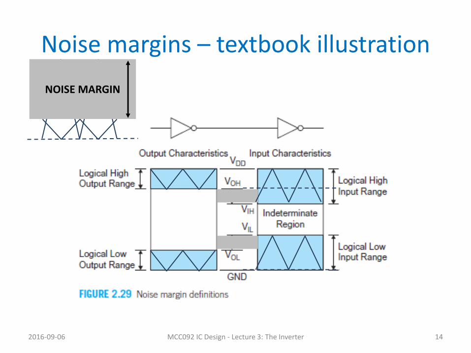
Noise margins – textbook illustration
2016-09-06 MCC092 IC Design - Lecture 3: The Inverter 14
NOISE MARGIN
Valid ”0”
Valid ”1”
2016-09-06 MCC092 IC Design - Lecture 3: The Inverter 15
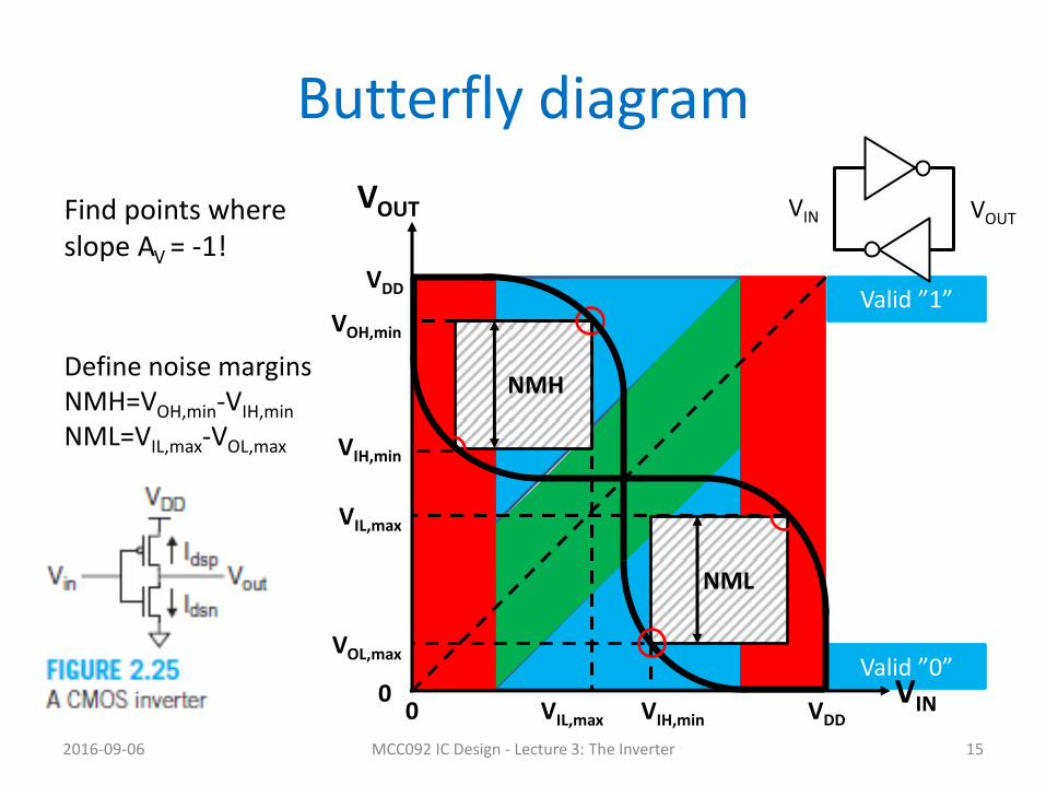
Butterfly diagram
VIN VDD
VOUT
VDD
0 0
Find points where slope AV = -1!
VOH,min
VOL,max
Define noise margins NMH=VOH,min-VIH,min
NML=VIL,max-VOL,max
NMH
NML
VIH,min VIL,max
VIL,max
VIH,min
VIN VOUT

Noise Margins – skewed inverters
2016-09-06 MCC092 IC Design - Lecture 3: The Inverter 16
NMH
NML
NML NMH

Matching MOSFET current characteristics
• Match the corresponding p-channel and n-channel MOSFET curves to each other!
MCC092 IC Design - Lecture 3: The Inverter 17 2016-09-06
VOUT
IDS
Fig. 2.26. Graphical derivation of CMOS inverter DC characteristics

Matching MOSFET current characteristics
MCC092 IC Design - Lecture 3: The Inverter 18 2016-09-06
Fig. 2.26. Graphical derivation of CMOS inverter DC characteristics
IDS
VOUT
IDS
VOUT
IDS
VOUT
IDS
VOUT
IDS
VOUT
Match the corresponding p-channel and n-channel MOSFET curves to each other!
VIN
VOUT
2016-09-06 MCC092 IC Design - Lecture 3: The Inverter 19
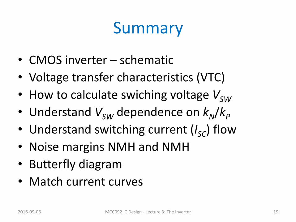
Summary
• CMOS inverter – schematic
• Voltage transfer characteristics (VTC)
• How to calculate swiching voltage VSW
• Understand VSW dependence on kN/kP
• Understand switching current (ISC) flow
• Noise margins NMH and NMH
• Butterfly diagram
• Match current curves
Valid ”0”
Valid ”1”
2016-09-06 MCC092 IC Design - Lecture 3: The Inverter 20
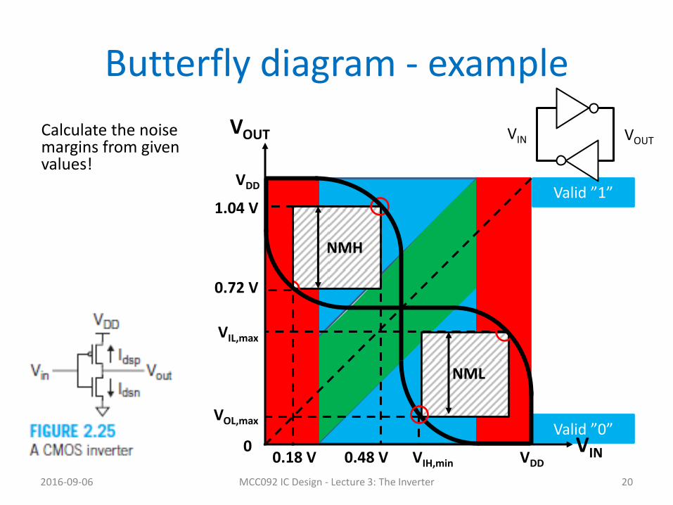
Butterfly diagram - example
VIN VDD
VOUT
VDD
0
Calculate the noise margins from given values!
1.04 V
VOL,max
NMH
NML
VIH,min 0.48 V
VIL,max
0.72 V
VIN VOUT
0.18 V
Valid ”0”
Valid ”1”
2016-09-06 MCC092 IC Design - Lecture 3: The Inverter 21
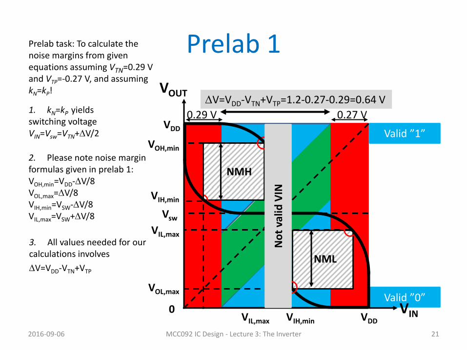
Prelab 1
VIN VDD
VOUT
VDD
0
Prelab task: To calculate the noise margins from given equations assuming VTN=0.29 V and VTP=-0.27 V, and assuming kN=kP!
VOH,min
VOL,max
2. Please note noise margin formulas given in prelab 1: VOH,min=VDD-DV/8 VOL,max=DV/8 VIH,min=VSW-DV/8 VIL,max=VSW+DV/8
NMH
NML
VIH,min VIL,max
VIL,max
VIH,min
DV=VDD-VTN+VTP=1.2-0.27-0.29=0.64 V 1. kN=kP yields switching voltage VIN=Vsw=VTN+DV/2
Vsw
3. All values needed for our calculations involves
DV=VDD-VTN+VTP
0.29 V 0.27 V
No
t va
lid V
IN

Lecture 3b The CMOS Inverter
Dynamic properties
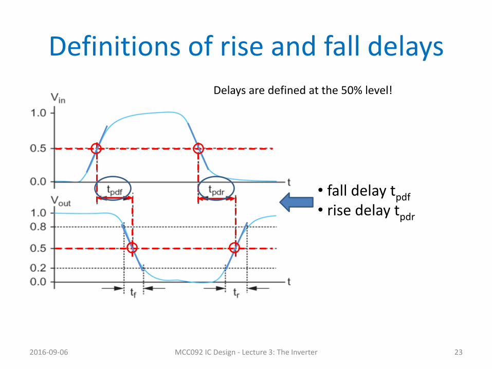
Definitions of rise and fall delays
2016-09-06 MCC092 IC Design - Lecture 3: The Inverter 23
• fall delay tpdf • rise delay tpdr
Delays are defined at the 50% level!
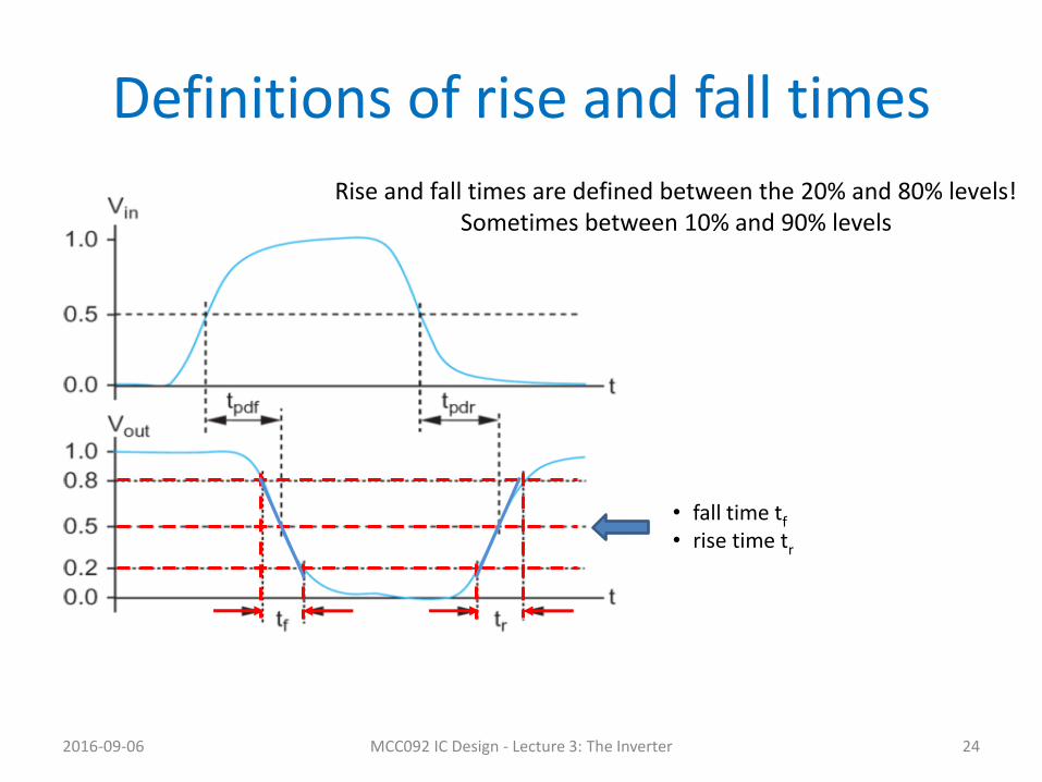
Definitions of rise and fall times
2016-09-06 MCC092 IC Design - Lecture 3: The Inverter 24
• fall time tf • rise time tr
Rise and fall times are defined between the 20% and 80% levels! Sometimes between 10% and 90% levels
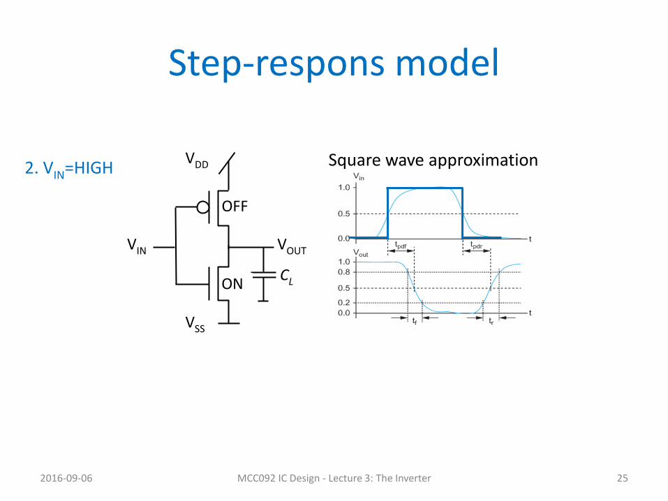
Step-respons model
2016-09-06 MCC092 IC Design - Lecture 3: The Inverter 25
VDD
VSS
CL
VIN VOUT
Square wave approximation
ON
OFF
1. VIN=LOW
OFF
ON
2. VIN=HIGH

Step-response model: rise delay
2016-09-06 MCC092 IC Design - Lecture 3: The Inverter 26
VOUT
VDD
IDSAT,P
Equivalent circuit
Load capacitance is charged through
p-MOSFET
1. VIN=LOW Square wave approximation
CL
, ,
L OUTpdr
DSAT P DSAT P
C VQt
I I
DD
DVOUT=VDD/2
VDD VDD/2
IDS,P
VOUT
IDSAT,P
pMOS current flow

Step-response model: fall delay
2016-09-06 MCC092 IC Design - Lecture 3: The Inverter 27
VOUT
CL
VSS
IDSAT,N
Equivalent circuit
Load capacitance is discharged through
n-MOSFET
2. VIN=HIGH
VDD VDD/2
IDS,N
VOUT
nMOS current flow
IDSAT,N
Square wave approximation
, ,
L OUTpdr
DSAT N DSAT N
C VQt
I I
DD
DVOUT=VDD/2
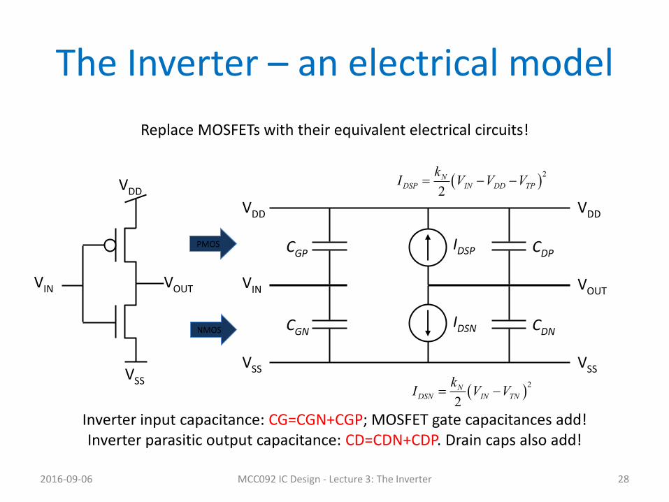
The Inverter – an electrical model
2016-09-06 MCC092 IC Design - Lecture 3: The Inverter 28
Replace MOSFETs with their equivalent electrical circuits!
NMOS
2
2
NDSN IN TN
kI V V
VIN VOUT
VSS
CGN
CDN
VSS
IDSN
VDD
CGP
CDP
VDD
IDSP
2
2
NDSP IN DD TP
kI V V V
Inverter input capacitance: CG=CGN+CGP; MOSFET gate capacitances add! Inverter parasitic output capacitance: CD=CDN+CDP. Drain caps also add!
VIN VOUT
VSS
VDD
PMOS

2
2
NDSN IN TN
kI V V
2
2
NDSP IN DD TP
kI V V V
The Inverter – an electrical model
2016-09-06 MCC092 IC Design - Lecture 3: The Inverter 29
VIN VOUT
VSS
VDD
VIN VOUT
VSS
CG=CGN+CGP
VSS
VDD VDD
CD=CDN+CDP
Inverter input capacitance: CG=CGN+CGP; MOSFET gate capacitances add! Inverter parasitic output capacitance: CD=CDN+CDP. Drain caps also add!
Since VIN is either VDD or VSS (GND) we can modify schematic accordingly
2
,max2
NDSP DD TP
kI V V
2
,max2
NDSN DD TN
kI V V
IDSN
IDSP
IDSN,max
IDSP,max
IDSP,max= 300 uA/um
IDSN,max= 600 uA/um

Problem
2016-09-06 MCC092 IC Design - Lecture 3: The Inverter 30
2
,max2
NDSP DD TP
kI V V
If IDSN,max is 600 mA/um in the 65 nm CMOS process from STMicroelectronics, what would be the effective kprime (kN´=mCox)?
In this process VDD= 1.2 V, VTN= 0.29 V, Cox= 20 fF/mm2, and Leff= 60 nm.
2
,max2
NDSN DD TN
kI V V
Answer: kN´=87 mA/V2, kN´=42 mA/V2
Similarly, if IDSP,max is 300 mA/um in the 65 nm CMOS process from STMicroelectronics, what would be the effective kprime (kN´=mCox)?
In this process VDD= 1.2 V, VTN= -0.27 V, Cox= 20 fF/mm2, and Leff= 60 nm.
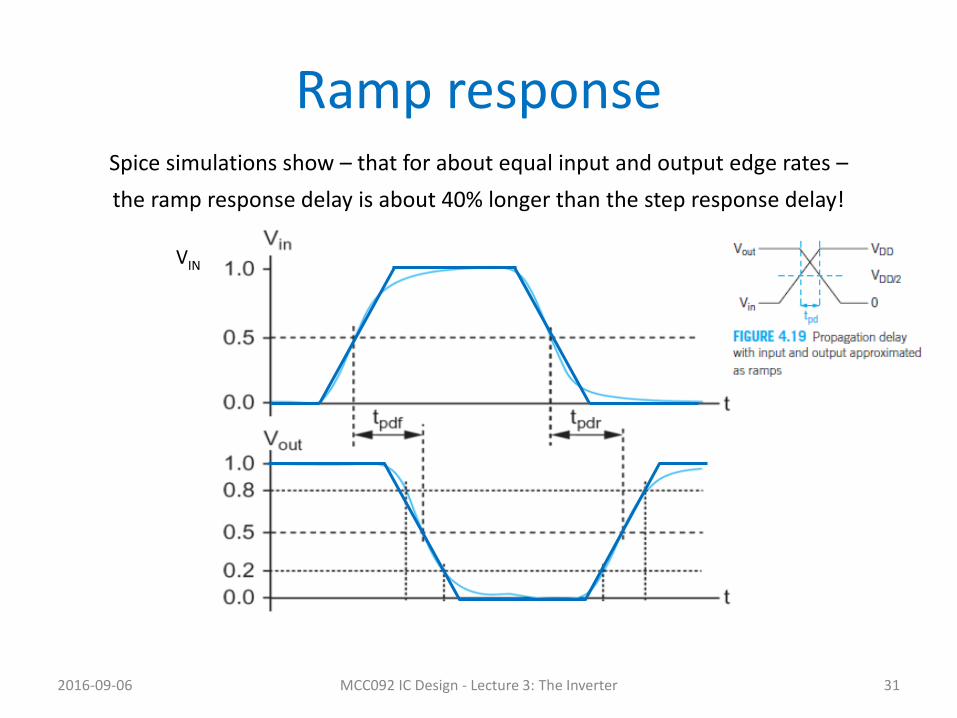
Ramp response
2016-09-06 MCC092 IC Design - Lecture 3: The Inverter 31
VIN
It is obvious that a ramp approximation would give a better model –
However, this is too complicated for simple analytical analysis
Spice simulations show – that for about equal input and output edge rates –
the ramp response delay is about 40% longer than the step response delay!
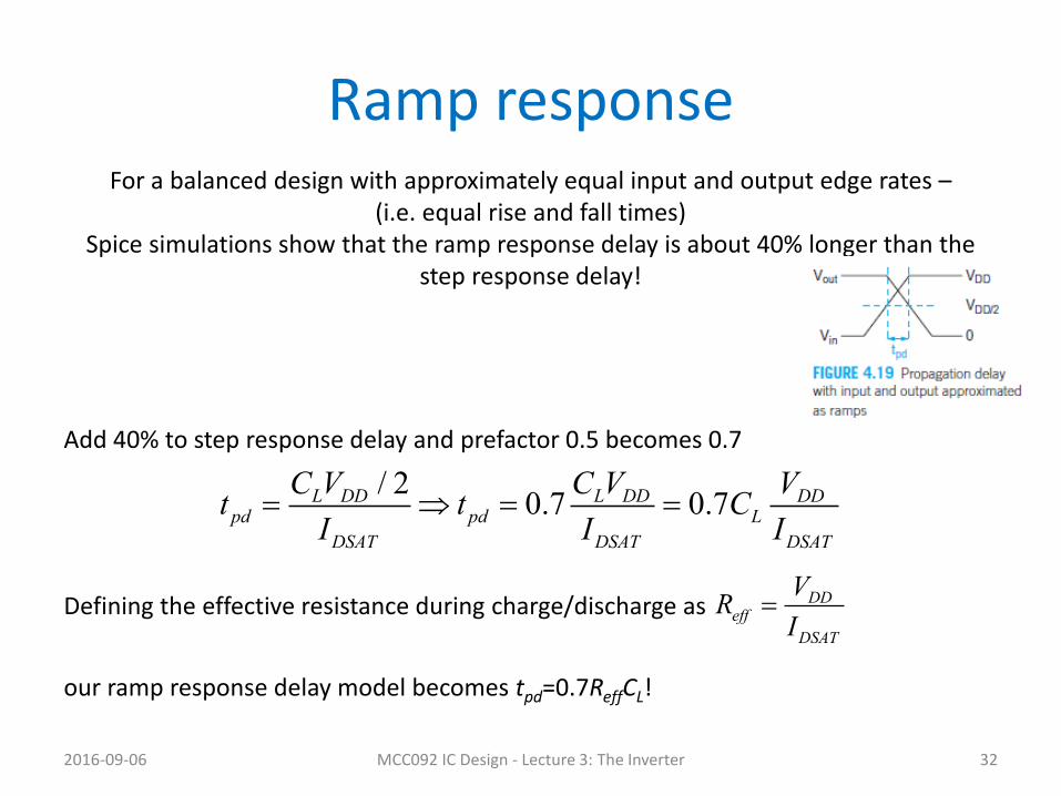
Ramp response
2016-09-06 MCC092 IC Design - Lecture 3: The Inverter 32
It is obvious that a ramp approximation would give a better model –
However, this is too complicated for simple analytical analysis
For a balanced design with approximately equal input and output edge rates – (i.e. equal rise and fall times)
Spice simulations show that the ramp response delay is about 40% longer than the step response delay!
/ 20.7 0.7L DD L DD DD
pd pd L
DSAT DSAT DSAT
C V C V Vt t C
I I I
Add 40% to step response delay and prefactor 0.5 becomes 0.7
DDeff
DSAT
VR
IDefining the effective resistance during charge/discharge as
our ramp response delay model becomes tpd=0.7ReffCL!
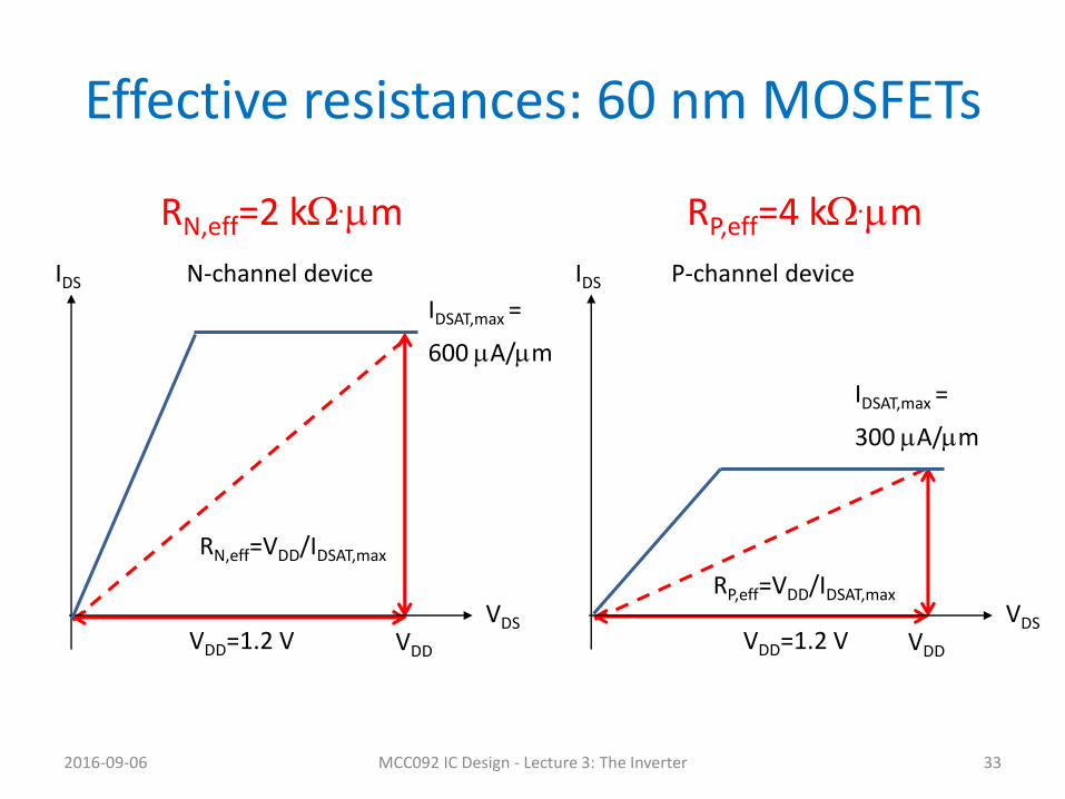
Effective resistances: 60 nm MOSFETs
2016-09-06 MCC092 IC Design - Lecture 3: The Inverter 33
RN,eff=VDD/IDSAT,max
RP,eff=VDD/IDSAT,max
RN,eff=2 kW.mm RP,eff=4 kW.mm
IDSAT,max =
600 mA/mm
VDD=1.2 V
N-channel device P-channel device
IDSAT,max =
300 mA/mm
VDD=1.2 V
IDS
VDS
IDS
VDS VDD VDD

Electrical ramp response model
2016-09-06 MCC092 IC Design - Lecture 3: The Inverter 34
Replace constant-current sources with effective resistances
VIN VOUT
VSS
VDD
VIN VOUT
VSS
CG
VSS
RN,eff
VDD VDD
RP,eff
RP,eff= 4 kW .mm
RN,eff= 2 kW .mm
CD

Ramp input – output response
2016-09-06 MCC092 IC Design - Lecture 3: The Inverter 35

Ramp input – output trace
2016-09-06 MCC092 IC Design - Lecture 3: The Inverter 36
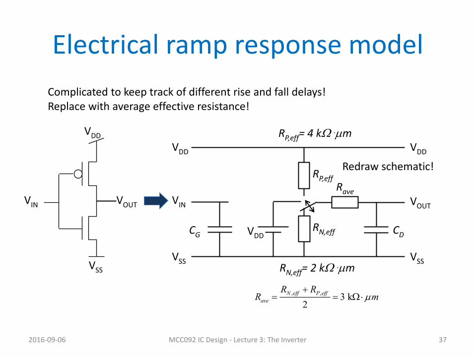
Electrical ramp response model
2016-09-06 MCC092 IC Design - Lecture 3: The Inverter 37
Complicated to keep track of different rise and fall delays! Replace with average effective resistance!
VIN VOUT
VSS
VDD
VIN VOUT
VSS
CG
VSS
VDD VDD RP,eff= 4 kW .mm
RN,eff= 2 kW .mm
CD
RN,eff
RP,eff
Rave
VDD
, ,3 k
2
N eff P eff
ave
R RR mm
W
Redraw schematic!

W´
2W´
VIN
Electrical ramp response model
2016-09-06 MCC092 IC Design - Lecture 3: The Inverter 38
Even better to resize p-channel device, i.e. to make it wider, so that RP,eff=RN,eff
VOUT
VSS
VDD
VIN VOUT
VSS
CG
VSS
CD
Rave
VDD
, ,2 k
2
N eff P eff
ave
R RR mm
W
Task: Calculate CG and CD!
Answer: Assuming L=60 nm and Cox=20 fF/mm2 we obtain CGN=1.2 fF and CGP=2.4 fF. Hence CG=3.6 fF. Concerning CD we assume CD=pCG=3.6 fF with p=1.
VDD
VSS
W=1 mm
W=2 mm
VOUT VIN
VIN
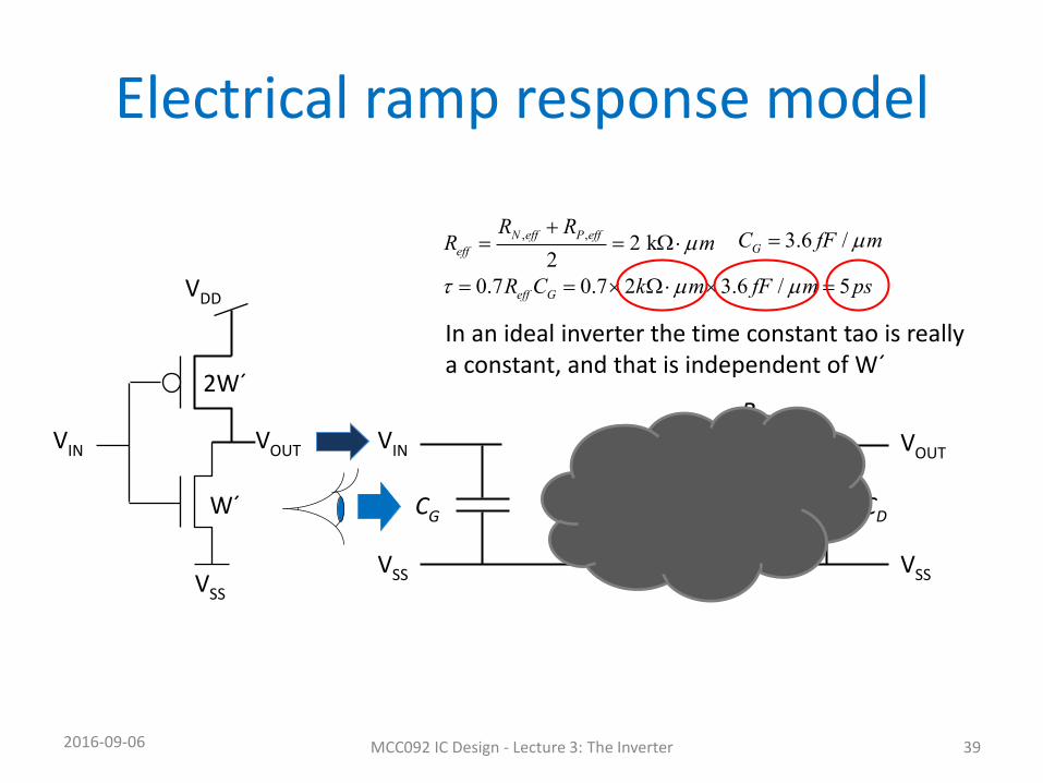
Electrical ramp response model
2016-09-06 MCC092 IC Design - Lecture 3: The Inverter 39
VOUT
VSS
VDD
VIN VOUT
VSS
CG
VSS
CD
Reff
VDD
, ,2 k
2
N eff P eff
eff
R RR mm
W
W´
2W´
3.6 /GC fF mm
0.7 0.7 2 3.6 / 5eff GR C k m fF m ps m m W
In an ideal inverter the time constant tao is really a constant, and that is independent of W´
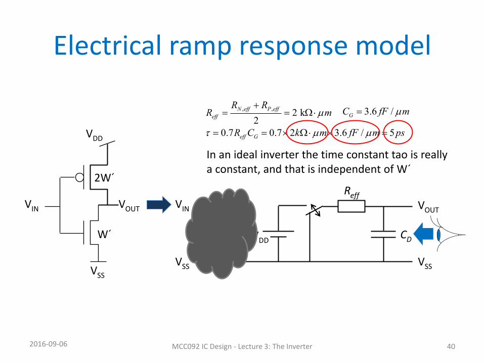
VIN
Electrical ramp response model
2016-09-06 MCC092 IC Design - Lecture 3: The Inverter 40
VOUT
VSS
VDD
VIN VOUT
VSS
CG
VSS
CD
Reff
VDD
, ,2 k
2
N eff P eff
eff
R RR mm
W
W´
2W´
3.6 /GC fF mm
0.7 0.7 2 3.6 / 5eff GR C k m fF m ps m m W
In an ideal inverter the time constant tao is really a constant, and that is independent of W´

Inverter pair delay
2016-09-06 MCC092 IC Design - Lecture 3: The Inverter 41
CG
Reff
VDD
Left-hand inverter sees a capacitive load CG!

Inverter pair delay
2016-09-06 MCC092 IC Design - Lecture 3: The Inverter 42
CG
Reff
CD
VDD
Right-hand inverter sees a driver with internal source resistance Reff and a parasitic capacitance CD!

Inverter pair delay
2016-09-06 MCC092 IC Design - Lecture 3: The Inverter 43
CG
Reff
CD
VDD
The propagation delay becomes effective resistance times load cap!
0.7 0.7 1 5 ps 2 10 pseff D G eff GR C C R C p
RC-circuit with delay RCxln2=0.7RC
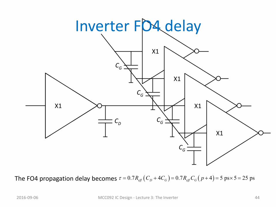
X1
X1
Inverter FO4 delay
2016-09-06 MCC092 IC Design - Lecture 3: The Inverter 44
CG
Reff
CD
VDD
X1 X1
The FO4 propagation delay becomes 0.7 4 0.7 4 5 ps 5 25 pseff D G eff GR C C R C p
X1
CG
CG
CG

X1
X1
Inverter FO4 delay
2016-09-06 MCC092 IC Design - Lecture 3: The Inverter 45
4CG
X1
The FO4 propagation delay becomes 0.7 4 0.7 4 5 ps 5 25 pseff D G eff GR C C R C p
X1
Reff
CD
VDD

Summary
• We defined rise and fall delays at the 50% level (VDD/2) • We defined rise and fall times between 20% and 80% levels • We calculated propagation delay in response to a square-wave input signal assuming
MOSFETs being saturated during delay • We improved the delay model by adding 40%
– assuming a ramp input signal and – assuming equal input and output edge rates
• We ”heard a bell ring” and replaced saturation current sources by effective resistances
• We made the p-channel MOSFET twice as wide to compensate for lower hole mobility (i.e. to compensate for kP´=kN´/2). – Both MOSFETs now have the same effective resistance of 2 kW.mm – However, p-channel device now has twice the input capacitance of the n-channel MOSFET
• We have obtained an electrical two-port model of the inverter for delay calculations – we know what this model looks like seen from the input port, and seen from the output port
• Finally, we calculated the FO4 delay, and we found the ReffCG product being independent of the inverter size (as long as we keep same ratio between WP and WN)
2016-09-06 MCC092 IC Design - Lecture 3: The Inverter 46


