1 The Dipole Moment Inversion Effects in Self-Assembled2 Nanodielectrics for Organic Transistors3 Binghao Wang,† Gabriele Di Carlo,†,‡ Riccardo Turrisi,†,§ Li Zeng,∥ Katie Stallings,† Wei Huang,†
4 Michael J. Bedzyk,∥ Luca Beverina,*,§ Tobin J. Marks,*,†,∥ and Antonio Facchetti*,†
5†Department of Chemistry and the Materials Research Center, Northwestern University, 2145 Sheridan Road, Evanston, Illinois
6 60208, United States7‡Department of Chemistry, University of Milan, INSTM Research Unit, Via C. Golgi 19, 20133 Milano, Italy
8§Materials Science Department, University of Milano-Bicocca, Via R. Cozzi 53, 20126, Milan, Italy
9∥Applied Physics Program, Materials Science and Engineering Department and Material Research Center, Northwestern University,
10 Evanston, Illinois 60208, United States
11 *S Supporting Information
12 ABSTRACT: We compare and contrast the properties of13 hybrid organic−inorganic self-assembled nanodielectrics14 (SANDs) based on alternating layers of solution-processed15 ZrOx and either of two phosphonic acid-functionalized16 azastilbazolium π-units having opposite dipolar orientations.17 Conventional Zr-SAND and new inverted IZr-SAND are18 characterized by Kevin probe, optical spectroscopy, capaci-19 tance−voltage measurements, AFM, X-ray reflectivity, and20 electronic structure computation. The molecular dipolar21 orientation affects thin-film transistor (TFT) threshold and22 turn-on voltages for devices based on either p-channel23 pentacene or n-channel copper perfluorophthalocyanine.24 Specifically, Zr-SAND shifts threshold and turn-on voltages25 to more positive values, whereas IZr-SAND shifts them in the opposite direction. Capping these SANDs with −SiMe3 groups26 enhances the effect, affording a 1.3 V difference in turn-on voltage for IZr-SAND vs Zr-SAND-gated organic TFTs. Such27 tunability should facilitate the engineering of more complex circuits.
28 ■ INTRODUCTION
29 In the growing field of organic electronics, a major challenge is30 providing reliable materials and methodologies for fabricating31 unconventional electronic devices.1−6 Organic thin-film tran-32 sistors (OTFTs) are of paramount interest, promising33 mechanical flexibility and facile solution processing.7,8 The34 semiconducting layer has been by far the most investigated35 OTFT component, although the other materials and interfaces36 are also critical to performance. In particular, plastic electronics37 applications require that the gate dielectric evolve from a38 conventional rigid metal oxide film (e.g., SiO2) to materials39 having a larger dielectric constant k, mechanical flexibility, and40 low voltage operation, as well as enabling fine-tuning of key41 device metrics such as threshold (VTH) and turn-on voltage42 (VON).
9,10 Viable SiO2 alternatives include metal oxides,43 electrolytes, self-assembled monolayers (SAMs) on metal44 oxides, and high-capacitance ultrathin/high-k polymers and45 polymer blends, each having their own strengths and46 limitations.11−18
47 Previously, we reported families of robust, structurally well-48 defined self-assembled nanodielectrics (SANDs) offering high49 capacitance, facile fabrication, and broad applicability to diverse
50semiconductors.19,20 Our most advanced SANDs consist of51alternating high-k metal oxide (ZrOx or HfOx) and highly52 f1polarizable, high-k PAE dipolar nanolayers (Figure 1a), all53processed from solution under ambient.21−23 To date, the54effects, if any, of PAE dipolar orientation on the dielectric55properties and OTFT response remain unknown. Here, we56address this issue using an “inverted” PAE unit, named IPAE,57to create a structurally inverted SAND (Figure 1b) and show58from Kevin probe measurements, molecular orbital computa-59tions, and OTFT measurements that dipolar inversion occurs60and that it affects, in an informative and useful way, the61principal OTFT parameters relevant to circuit design and62fabrication.24,25
63■ EXPERIMENTAL SECTION64IPAE Synthesis and Characterization. All reagents are65commercially available and were used without further purification66unless otherwise stated. Anhydrous dichloromethane was distilled
Received: August 10, 2017Revised: November 8, 2017Published: November 10, 2017
This is the pre-peer reviewed version of the following article: 1B. Wang, G. Di Carlo, R. Turrisi, L. Zeng, K. Stallings, W. Huang, M. J. Bedzyk, L. Beverina, T. J. Marks and A. Facchetti, Chem. Mater., 2017, 29, 9974–9980., which has been published in final form at [https://pubs.acs.org/doi/10.1021/acs.chemmater.7b03397]. This article may be used for non-commercial purposes in accordance with Wiley Terms and Conditions for Use of Self-Archived Versions
67 from calcium hydride, whereas toluene was distilled from Na/68 benzophenone. Unless otherwise stated, all reactions were carried69 out under N2 using standard Schlenk line techniques. Details of IPAE70 synthesis are given in the Supporting Information. UV−vis spectra71 were recorded on a Varian Cary 50 Scan UV−vis spectrophotometer.72 Microwave enhanced reactions were performed in a CEM Discover73 Instrument working under Dynamic conditions. NMR spectra were74 recorded on a Varian Unity Plus 500 (500 MHz, room temperature)75 spectrometer, and chemical shifts are referenced to TMS for 1H and76 internally calibrated by the spectrometer for 31P.77 SAND Film Growth. ZrOx solutions for the deposition of ZrOx78 layers were prepared by dissolving 93.2 mg of ZrCl4 (Sigma-Aldrich)79 in 4.0 mL of absolute ethanol, affording a 0.1 M solution. After 5 min80 of stirring, 300 mg of 68% wt./wt. HNO3 was added and the solution81 was heated at 60 °C for 3 h, then aged at room temperature for 12 h.82 From this mother solution, 0.01 and 0.02 M solutions were prepared83 by dilution with ethanol for future use. The substrates (glass or n+2-Si/84 native SiO2) were cleaned by sonication in acetone, hexane, and85 ethanol for 5 min, followed by air plasma cleaning (400−500 mTorr)86 for 5 min. Growth of the dielectric stacks was carried out in a Class-1087 HEPA filtered laminar flow clean hood (NuAire) to minimize88 contamination. All solutions were filtered through 0.2 μm Teflon89 syringe filters. Growth of Zr-SAND and IZr-SAND films was carried90 out in the following these steps: Step 1 (ZrOX-Primer): The ZrOx91 primer layer was prepared by spin-coating the 0.02 M precursor92 solution at 5000 rpm for 30 s, then baking the coated substrate at 22093 °C for 20 min. Step 2 (PAE/IPAE Self-Assembly): The organic94 molecular layer was self-assembled on the surface by immersing the95 primer-coated substrate in a 3 mM methanol solution of the96 azastilbazolium reagent of interest, PAE for Zr-SAND and IPAE for97 IZr-SAND, for 1 h at 60 °C.26 The films were then cleaned by98 sonication in methanol for 5 s using two different methanol baths. Step99 3 (ZrOx-Capping): The capping layer was fabricated by spin-coating100 the 0.01 M precursor solution at 5000 rpm for 30 s, then baking at 220101 °C for 20 min. The last two steps (self-assembly + ZrOx capping) were102 repeated in sequence to achieve the desired number of SAND layers.103 The HMDS-capped cZr-SAND and cIZr-SAND films were fabricated104 by spin-coating pure HMDS on top of 4 layers Zr-SAND and IZr-105 SAND films. (5000 rpm, 30 s), followed by annealing at 130 °C for 20106 min.107 SAND Film Characterization. X-ray reflectivity (XRR) was108 performed on an 18 kW Rigaku ATXG diffractometer workstation109 with Cu Kα radiation (λ = 1.54 Å). The reflectivity data for the IZr-110 SAND thin films are plotted as a function of momentum transfer (Q =111 4π sin(θ)/λ) and fitted with the Motofit/Igor software package to112 extract the film thickness and electron density profile. Kelvin Probe113 measurements were carried out on an Ambient Kelvin Probe System114 (KP technology, USA). The humidity was ∼22%. The reference115 electrode was gold. SAND film UV−vis spectra were recorded on a116 Varian Cary 50 Scan spectrophotometer. FT-IR spectra were collected117 on a Nexus 870 spectrometer (Thermo Nicolet) with a single
118reflection horizontal ATR accessory having a diamond ATR crystal119fixed at a 45° incident angle.120Electrical Measurements on SAND Films. To fabricate metal−121insulator−semiconductor capacitors, gold contacts were thermally122evaporated at a 0.3 Å/s rate from a base pressure of 3 × 10⁻⁶ Torr123through 200 μm × 200 μm shadow masks. MIS characterization was124performed under ambient conditions using an Agilent B1500A125semiconductor parameter analyzer. Leakage current density vs voltage126(J−V) curves, areal capacitance vs voltage (C−V) curves, and areal127capacitance vs frequency (C−f) curves were recorded under ambient128conditions using a flexible tungsten 1 μm whisker probe (SE-SM,129Signatone) as a cathode and a beryllium−copper alloy probe (SE-BC,130Signatone) as an anode. C−V curves were tested at 10 kHz. The131multilayer dielectric in the n+2-Si/Zr-SAND [primer ZrO2/(PAE/132capping ZrO2)n, n (number of bilayers) = 1, 2, 3, and 4]/Au MIS133devices can be modeled as capacitors in series, according to eq 1. Here,134SiO2 is the native oxide on the Si wafer, p-ZrO2 is the ZrO2 primer135layer,
= + + · +‐ ‐
⎛⎝⎜⎜
⎞⎠⎟⎟
⎛⎝⎜⎜
⎞⎠⎟⎟C C C
nC C
1 1 1 1 1
i SiO p ZrO Org c ZrO2 2 2 136(1)
137c-ZrO2 is the ZrO2 capping layer, and Org is the PAE or IPAE layer.138The capacitances of the native oxide and ZrO2 primer layer on the n
+2-139Si bottom electrode are 2236 and 4425 nF/cm2, respectively, assuming140a 1.5 nm thick SiO2 (k = 3.9) and 2 nm thick ZrO2 layer (k = 10).141Organic Thin-Film Transistor Fabrication and Character-142ization. Pentacene (P5, 99%, Sigma-Aldrich) and copper perfluor-143ophthalocyanine (F16CuPc, 98%, TCI Chemicals) were sublimed twice144(base pressure: 7.0 × 10⁻⁶ Torr) in a three-zone sublimer prior to use.145Temperatures for pentacene: 290, 275, 230 °C. Temperatures for146F16PcCu: 460, 400, 300 °C. Semiconductor films (50 nm thick) were147patterned during thermal evaporation (0.1 Å/s, base pressure 3.5 ×14810−6 Torr) through 5 mm × 8 mm shadow masks. The substrates were149kept at 25 °C for P5 evaporation and at 125 °C for F16CuPc150evaporation. OTFT fabrication was completed by thermal evaporation151(50 nm, 0.3 Å/s, base pressure 3 × 10⁻⁶ Torr) of gold contacts (W = 5152mm, L = 100 μm). Transfer and output plots were recorded using an153Agilent B1500A semiconductor parameter analyzer. Carrier mobilities154(μ) were evaluated in the saturation regime with a conventional155metal−oxide−semiconductor field-effect transistor model. The156capacitance of Zr-SAND/cZr-SAND and IZr-SAND/cIZr-SAND157used for mobility calculations are 465/352 and 503/394 nF cm−2
158(measured at 104 Hz), respectively.
159■ RESULTS AND DISCUSSION160Here, we first report the design and synthesis of the new IPAE161building block for nanodielectric films, then fabricate in parallel,162conventional Zr-SAND and inverted IZr-SAND films. These163dielectric films are characterized by several methods including164optical, electrical, and morphological measurements. In165addition, the dipolar inversion is investigated by Kevin probe166techniques and DFT computation, corroborating inversion of167the dipole. Finally, p-/n-channel OTFTs are fabricated and the168device performance parameters discussed in detail, including169how they vary with SAND and organic semiconductor170microstructure.171Synthetic Strategy for Inverted SANDs. The design and172synthesis of an inverted PAE analogue having similar173 s1connectivity, IPAE, is shown in Scheme 1. Note that, although174the π-conjugated azastilbazolium cores of PAE and IPAE are175identical, there are minor differences in the structures such as176larger distance between the phenylphosphonic acid portion and177the core (1 atom in PAE and 2 atoms in IPAE) and, more178evident, two hydroxylethyl fragments in the latter versus one in179the former structure. However, the hydroxyethyl group is not180the anchoring point of the chromophore to the surface but is
Figure 1. Dielectric stacks comprising four-chromophore/ZrOx layerson top of the ZrOx (p-ZrOx) primer film. (a) Conventional Zr-SANDwith a phosphonate π-electron (PAE) unit. (b) Inverted IZr-SANDwith an inverted PAE (IPAE) π-unit.
181 simply used to achieve good chemical adhesion to the overlying182 ZrOx layer. More importantly, it does not drive the self-183 assembly process as judged from the kinetics of PAE/IPAE184 absorption, which are governed by the phosphonic acid185 fragment and are identical for the two systems (vide inf ra).186 The IPAE synthesis begins with the nucleophilic attack of N-187 methylaniline 2 on the benzylic position of 4-bromobenzyl188 bromide 1. The resulting amine 3 is then employed in diazo189 coupling with pyridine moiety 4. Traditional approaches were190 unsuccessful to afford 5 with acceptable yields.27−30 However,191 the generation of diazonium salt by aqueous HBF4 + NaNO2192 produces the N-asymmetric azabenzenes in high yields.31 The193 structure of 5 was confirmed by single-crystal diffraction (see194 the Supporting Information). Surprisingly, functionalization of195 5 with a diethyl-phosphonate group was unsuccessful via either196 Pd-catalyzed Hirao or Ni-catalyzed coupling.32,33 Thus,197 Finkelstein halide exchange was used to obtain iodo derivative198 6, which was then converted into phosphonate 7 under Hirao
199conditions. Alkylation of 7 to give 8 in neat 2-bromoethanol200under microwave irradiation, followed by phosphonic ester201cleavage with Me3SiBr, affords phosphonic acid IPAE in good202yield. Characterization by elemental analysis, NMR, and single-203crystal diffraction of IPAE and synthetic intermediates are204presented in Figures S1−S7 and Tables S1−S7. As noted205above, the IPAE double hydroxyethyl group is not the206chromophore anchoring point to the surface but is used to207achieve good chemical adhesion to the top ZrOx layer.208 f2Figure 2a shows IPAE and PAE optical spectra in methanol209solution. The former features a hypsochromic shift of ∼20 nm210in λmax and half the molar extinction coefficient ε of PAE211 t1(Table 1). This result likely reflects the different roles of the212phosphonic acid electron-withdrawing residue in the two213molecules. Thus, the PO(OH)2 moiety increases the “pull”214character of the electron-poor pyridinium moiety in PAE,215increasing the oscillator strength along the molecular axis and216red-shifting λmax. In contrast, the electron-withdrawing effect in217IPAE decreases the charge density on the amine “push”218nitrogen, thus decreasing the total oscillator strength and the219donor−acceptor coupling. Note that the presence of a220phosphonic acid (pKa1 ∼ 1−2) and an azo bridge base (pKa221∼ 3−4) in the same molecule imparts halochromic properties,222typical of aromatic azo compounds such as the pH indicator223methylorange.34,35 Concentrated polar IPAE solutions (>0.1224M) appear red, while dilution increases the pH and λmax shifts225toward that observed in Figure 2a.226SAND Film Characterization. UV−vis-monitored kinetic227measurements (Figure 2b) indicate that PAE and IPAE have228comparable grafting rates on the ZrOx surface of glass/ITO/229ZrOx substrates and reach maximum SAM densities after ∼60230min at 60 °C (data points normalized to ε). IZr-SAND231fabrication of n-bilayers (from 1 to 4) is similar to that reported232for conventional Zr-SANDs, with the IZr-SAND optical233absorption on glass at 547 nm increasing linearly with the234number of bilayers, and FT-IR spectra clearly demonstrating
Scheme 1. Synthesis of Inverted SAND Building Block IPAE
Figure 2. (a) Normalized optical absorption spectra of PAE and IPAE in MeOH. (b) Optical spectroscopic data as a function of monolayer self-assembly time. (c) Contact potential difference (CPD) for p-ZrOx/Si, PAE/p-ZrOx/Si, and IPAE/p-ZrOx/Si films. (d) Illustration of the differentpolarization directions for PAE and IPAE. (e) Reciprocal of capacitance vs the number of SAND layers with the corresponding linear fit indicated bythe broken lines; Inset: Corresponding areal capacitance vs the number of layers. Representative (f) C−V curves (measured at 104 Hz), (g) C−fcurves (measured at 3.5 V), and (h) J−V plots for Zr-SAND and IZr-SAND (n = 4). In all MIS measurements, the metal is grounded.
235 the CH2 stretching (2920 and 2850 cm−1) and arene ring236 vibrational modes (1580, 1230, and 878 cm−1) (Figure S8).237 Before IZr-SAND fabrication and characterization, the238 inversion in the surface dipole was assessed experimentally by239 Kelvin probe analysis and theoretically by DFT calculations.240 The Kelvin probe measures the contact potential difference241 (CPD) between a reference surface (gold) and the sample.36
242 Thus, the CPD values (Figure 2c) of PAE/Primer ZrOx (PAE/243 p-ZrOx) (∼ −983 meV) is more negative than that of IPAE/244 Primer ZrOx (IPAE/p-ZrOx) (∼ −463 meV), with that of the245 primer ZrOx located in between (∼ −770 meV). This result246 substantiates dipole inversion and is in agreement with the247 pictorial orientation toward the surface (Figure 2d), thus248 facilitating electron extraction and decreasing the CPD value.249 Furthermore, the different directions of PAE and IPAE SAM250 dipole moments is supported by MO computations (Figure S9,251 Table S8, vide inf ra). Together, these data argue that the252 chromophore components of the SAND/ISANDs should253 produce opposite built-in electric fields.37,38
254 SAND Dielectric and Electrical Properties. To assess the255 dielectric properties of these hybrid ZrOx−azastilbazolium256 stacks, SANDs were fabricated on n+2-Si substrates using PAE257 (Zr-SAND) and IPAE (IZr-SAND), following an iterative258 process of sol−gel ZrOx spin-casting, thermally assisted259 densification at 220 °C in air, and immersion-grafting in260 methanol (details in the SI and AFM images in Figure S10). X-261 ray reflectivity of the 4-Layer IZr-SAND and Zr-SAND262 demonstrate almost identical thickness, 12.2 and 12.1 nm,
263respectively (Table 1, Figure S8). Metal−insulator−semi-264conductor (MIS) capacitors were fabricated by gold electrode265thermal deposition (device area = 200 μm × 200 μm) on Zr-266SAND and IZr-SAND (details in the SI). The capacitance267shows linear dependence on the number of layers (n) (Figures2682e and S11), confirming the regular multilayer structures of the269PAE- and IPAE-based SANDs. These data indicate that the270capacitance values of the IZr-SANDs are slightly larger than271those of the corresponding Zr-SANDs, attributed to the slightly272different molecular structure and opposite the built-in polar-273ization orientation (Table 1).274Regarding capacitance response with voltage (Figures 2f and275S11), note the following: (a) The effects of the PAE vs IPAE276structure on the dielectric stack capacitance manifest277themselves in slightly higher values for IZr-SAND stacks vs278Zr-SAND stacks and by different dC/dV values in the279accumulation regime (Figure S12); these data can be280interpreted by considering that, during the capacitance281measurement, the molecular dipole in IZr-SAND is oriented282with the applied field effectively promoting positive/negative283charge localizations at the top/bottom interfaces (Figure 2d).284(b) The voltage onset of accumulation is more negative for IZr-285SANDs [−400 to +300 mV] than for Zr-SANDs [−100 to286+250 mV], which is in agreement with the different built-in287polarization of the two nanodielectric types (Table S9).39
288Figure 2g shows the C−f curves for 4-layer Zr-SAND and IZr-289SAND dielectrics, indicating that the latter exhibit stable290capacitance to a greater frequency range (1 × 10⁵ Hz) than the
Table 1. Optical Properties of PAE Derivatives and Dielectric Properties of IZr-SAND and Zr-SAND Stacks with DifferentNumbers of (Bi)layers
adXRR = thickness established by X-ray reflectivity. bkorg is the dielectric constant of PAE or IPAE.
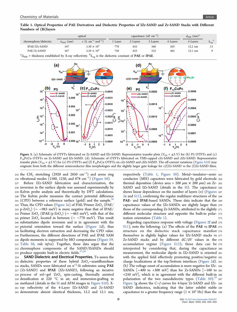
Figure 3. (a) Schematic of OTFTs fabricated on Zr-SAND and IZr-SAND. Representative transfer plots (VDS = ±3 V) for (b) P5 OTFTs and (c)F16PcCu OTFTs on Zr-SAND and IZr-SAND. (d). Schematic of OTFTs fabricated on TMS-capped cZr-SAND and cIZr-SAND. Representativetransfer plots (VDS = ±3 V) for (e) P5 OTFTs and (f) F16PcCu OTFTs on cZr-SAND and cIZr-SAND. The off-current variations (Figure S18) mayoriginate from both the different semiconductor film morphologies and the slightly larger gate leakage for c(I)Zr-SAND vs the (I)Zr-SAND films.
291 former (3 × 10⁴ Hz). The leakage currents of 4-layer Zr-SAND292 and IZr-SAND (Figure 2f) are ∼1−2 × 10⁻⁶ A cm−2 at 3 V,293 albeit those of IZr-SAND are statistically slightly larger,294 comparable to other ZrOx- and HfOx-based PAE dielec-295 trics.20,23
296 Thin-Film Transistors. To probe dipole inversion effects297 on charge transport and VTH/VON, 4-layer IZr-SAND and Zr-298 SAND stacks were used to fabricate bottom-gate, top-contact299 OTFTs by evaporating pentacene (P5, p-type) or Cu300 perfluorophthalocyanine (F16PcCu, n-type) films and Au S/D301 contacts (W = 5 mm, L = 100 μm; full details in the SI). The
f3 302 OTFT architecture is shown in Figure 3a, while the associated303 transfer plots measured at ±3 V are in Figure 3b,c. Key TFT
t2 304 parameters are summarized in Table 2. P5 and F16PcCu TFTs305 carrier mobilities on both types of SANDs are large (0.4−0.6306 and 0.05−0.06 cm2 V−1 s−1, respectively)greater than307 previously reported for similar OTFT achitectures.16 Note308 that, since semiconductor morphology is not affected by the309 SAND type (vide inf ra), carrier mobility in saturation should310 and does remain similar for the two SANDs. However,311 importantly, both semiconductors exhibit a negative VTH/VON312 shift, from −50 to −700 mV, on going from Zr-SAND to IZr-313 SAND (Table 2). To verify that these shifts are not314 morphology-related, AFM images of P5 and F16PcCu films315 on IZr- and Zr-SAND were recorded and indicate no major316 differences (Figure S13), exhibiting typical vapor-deposited P5317 and F16PcCu crystallites. Note that, on average, the VON shift318 (−150 mV for P5 and −500 mV for F16PcCu) is larger than the319 VTH shift [−50 mV for P5 and −300 mV for F16PcCu], in320 agreement with other studies investigating effect polarity and321 dipole orientation effects on the transport characteristics of322 organic semiconductors.40,41 Also, comparing the VTH of P5323 OTFTs based on 3L- and 4L-IZr-SAND, note that the VTH324 shifts positive from 3L to 4L-SANDs (Figure S14),325 demonstrating the more prominent dipole effect of the latter.326 Interestingly, Kelvin probe measurements (Figure S15)327 indicate that the CPD values of the PAE/p-ZrOx or IPAE328 layer capped with a ZrOx film (structures equivalent to a 1L Zr-329 SAND/IZr-SAND films) are almost identical to the primer330 ZrOx (p-ZrOx), suggesting that the surface potential difference331 between the two types of chromophores is moderated on332 capping. To understand whether there is a dampening effect on333 VTH/VON due to the uppermost ZrOx capping layer, OTFTs334 were fabricated minus the top ZrOx layer but with Me3Si-335 capping of the exposed organic hydroxyl groups to yield cZr-336 SAND and cIZr-SAND (Figure 3d). The device data (transfer
337plots in Figure 3e,f) indicate two interesting trends on replacing338the ∼1 nm ZrOx cap with Me3Si− groups. The leakage currents339(Figure S16a) of cZr-SAND and cIZr-SAND are ∼2−4 × 10⁻⁶
340A cm−2 at −3 V, slightly higher than those of the corresponding341Zr-SAND and IZr-SAND. The C−f plots (Figure S16b) exhibit342obvious frequency dependence even at low frequencies,343indicating Me3Si− capping cannot prevent ion motion in344PAE and IPAE layers. Note that a clear onset voltage difference345in the capacitance measurements can be detected by measuring346cZr-SAND vs cIZr-SAND (−0.09 vs 0.16 V), thus eliminating347the dampening effect from ZrOx capping layer (Figure S16c).348With regard to the OTFT performance, first, the carrier349mobilities of both semiconductors fall [0.2−0.03 cm2 V−1 s−1
350for P5 and ∼10−3 cm2 V−1 s−1 for F16PcCu] as a result of non-351optimal semiconductor film morphology (Figure S17),352indicated by far smaller grains than in the ZrOx-capped353SANDs. Specifically, the F16PcCu AFM phase images show sub-35450 nm crystallites with abundant grain boundaries, and355complete loss of contiguity in the semiconducting layer. We356infer that the different substrate surface energies and closer357proximity of the molecular dipole to the interface may induce a358non-optimal semiconductor growth morphology, particularly359near the dielectric surface in the channel region. Second, and360most important, the dipole inversion-related VTH/VON shifts361increase significantly as the result of the closer coupling362between the dipolar component of the SAND stack and the363semiconductor. Thus, in the P5 OTFTs, replacing the ZrOx364capping layer with Me3Si− induces significant dipole inversion365VTH and VON shifts of −650 and −1300 mV, respectively. For366the F16PcCu-based devices, both VTH/VON shifts are ∼ −700367mVlarger than that measured for the ZrOx-capped SANDs;368however, the VTH shift is not as dramatic as for P5. This result369may reflect the limited accuracy of the OTFT parameters for370the low-mobility F16PcCu devices on cIZr-SAND as well as the371limited significance of VTH shifts when comparing devices with372very different electrical characteristics,40,42−44 as for P5 OTFTs373on the same dielectric. Note also that the slower P5 turn-on374(larger subthreshold swing) on Zr-SAND and its incomplete375saturation may obscure the comparison between these different376gate dielectrics.377The direction of the present VTH/VON shifts parallels those of378other SAM dipole inversion experiments,42,45,46 consistent with379an IPAE dipole inversion vs PAE. Using the cIZr-SAND versus380IZr-SAND ΔVON parameters, it should be possible to estimate381the dipole direction from ΔV = NP⊥/ε0k, where N and k are382the surface density and the dielectric constants of the organic
Table 2. Electrical Parameters for OTFTs Fabricated with the Indicated Four-Layer ZrOx Based SANDsa
OTFT structure of Figure 3ab OTFT structure of Figure 3dc
ΔVON (mV) −150 −500 −1300 ∼ −700SS (V/dec) 0.18 ± 0.01 0.18 ± 0.02 1.26 ± 0.04 1.20 ± 0.03 0.40 ± 0.05 0.20 ± 0.02 ∼2d ∼2daValues represent the average of 10+ devices and are reported with relative uncertainties; the mobility values in parentheses are the maximum values.bZrOx-capped four-layer Zr-SANDs and IZr-SANDs. cMe3Si-capped four-layer cZr-SANDs and cIZr-SANDs. dApproximate due to the low μ valuesand ION/IOFF ratios.
383 SAMs (Table 1), and P⊥ is the molecular dipole moment along384 the molecular long axis. Taking into account the presence of385 four organic layers, P⊥ along the substrate normal for IPAE and386 PAE layers is therefore estimated to be +2.00 D and −1.45 D,387 respectively. A positive sign indicates dipolar orientation from388 the Si substrate to the film surface, in agreement with dipole389 inversion as depicted in Figure 1.46 Note that these results are390 in accord with the P⊥ found here for IPAE (+0.70 D) and PAE391 (−3.04 D), estimated by combining long-period X-ray standing392 wave experiments47 and DFT computations (Figure S9), as393 well as previous identification of gate dielectric dipolar effects in394 very different materials.10,45 Note that the counterion should395 also affect the chromophore polarizability and we are now396 exploring other anions.
397 ■ CONCLUSIONS398 A “dipole inverted” phosphonic acid-functionalized azastilbazo-399 lium molecule (IPAE) was synthesized and characterized, and400 the resulting IZr-SAND properties were investigated by a401 battery of techniques. It is shown that the threshold and turn-402 on voltages of p- and n-type OTFTs based on ZrOx-derived403 SANDs can be tuned by manipulating the phosphonate dipolar404 orientation and proximate dielectric functionality. We believe405 that SAND dipole modulation, along with new semiconductor406 design and device engineering, can further advance optoelec-407 tronic device performance. Future efforts include exploration of408 different counterions, whose structure can greatly impact the409 overall dipole moment strength and direction, as well as410 fabricating these structures in a cleanroom and using all-411 patterned layers for detailed statistical analysis.
412 ■ ASSOCIATED CONTENT413 *S Supporting Information414 The Supporting Information is available free of charge on the415 ACS Publications website at DOI: 10.1021/acs.chemma-416 ter.7b03397.417 Full experimental procedures, AFM images, NMR418 spectra, UV−vis spectra, capacitance data, crystallo-419 graphic data, and DFT computations (PDF)
420 ■ AUTHOR INFORMATION421 Corresponding Authors422 *E-mail: [email protected] (A.F.).423 *E-mail: [email protected] (T.J.M.).424 *E-mail: [email protected] (L.B.).425 ORCID426 Gabriele Di Carlo: 0000-0002-8782-7945427 Li Zeng: 0000-0001-6390-0370428 Wei Huang: 0000-0002-0973-8015429 Michael J. Bedzyk: 0000-0002-1026-4558430 Luca Beverina: 0000-0002-6450-545X431 Tobin J. Marks: 0000-0001-8771-0141432 Funding433 This work was supported by the BSF (AGMT-2012250), the434 MRSEC program of the National Science Foundation (DMR-435 1121262), and ONR (MURI N00014-11-1-0690). A.F. thanks436 the Shenzhen Peacock Plan project (KQTD20140437 630110339343) for financial support. This work made use of438 the J. B. Cohen X-ray Diffraction Facility, EPIC facility, Keck-II439 facility, and SPID facility of the NUANCE Center at440 Northwestern U., which received support from the Soft and
441Hybrid Nanotechnology Experimental (SHyNE) Resource442(NSF NNCI-1542205); the MRSEC program (NSF DMR-4431121262) at the Materials Research Center; the International444Institute for Nanotechnology (IIN); the Keck Foundation; and445the State of Illinois, through the IIN.
446Notes447The authors declare no competing financial interest.
448■ ACKNOWLEDGMENTS449We specially thank Mr. Bo Fu and Professor Mark A. Ratner of450Northwestern University for the DFT computations.
451■ REFERENCES(1) 452Xu, Y.; Sun, H.; Shin, E. Y.; Lin, Y. F.; Li, W. W.; Noh, Y. Y.
453Planar-Processed Polymer Transistors. Adv. Mater. 2016, 28, 8531.(2) 454Shankar, S.; Lahav, M.; van der Boom, M. E. Coordination-Based
455Molecular Assemblies as Electrochromic Materials: Ultra-High Switch-456ing Stability and Coloration Efficiencies. J. Am. Chem. Soc. 2015, 137,4574050.
(3) 458Osaka, I.; Takimiya, K. Backbone orientation in semiconducting459polymers. Polymer 2015, 59, A1.
(4) 460Zhang, L.; Colella, N. S.; Cherniawski, B. P.; Mannsfeld, S. C. B.;461Briseno, A. L. Oligothiophene Semiconductors: Synthesis, Character-462ization, and Applications for Organic Devices. ACS Appl. Mater.463Interfaces 2014, 6, 5327.
(5) 464Stalder, R.; Mei, J. G.; Graham, K. R.; Estrada, L. A.; Reynolds, J.465R. Isoindigo, a Versatile Electron-Deficient Unit For High-Perform-466ance Organic Electronics. Chem. Mater. 2014, 26, 664.
(7) 471D’Innocenzo, V.; Luzio, A.; Abdalla, H.; Fabiano, S.; Loi, M. A.;472Natali, D.; Petrozza, A.; Kemerink, M.; Caironi, M. Two-dimensional473charge transport in molecularly ordered polymer field-effect474transistors. J. Mater. Chem. C 2016, 4, 11135.
(8) 475Mukhopadhyay, T.; Puttaraju, B.; Senanayak, S. P.; Sadhanala, A.;476Friend, R.; Faber, H. A.; Anthopoulos, T. D.; Salzner, U.; Meyer, A.;477Patil, S. Air-Stable n-channel Diketopyrrolopyrrole Diketopyrrolopyr-478role Oligomers for High Performance Ambipolar Organic Transistors.479ACS Appl. Mater. Interfaces 2016, 8, 25415.
(9) 480Kirsch, P. D.; Sivasubramani, P.; Huang, J.; Young, C. D.;481Quevedo-Lopez, M. A.; Wen, H. C.; Alshareef, H.; Choi, K.; Park, C.482S.; Freeman, K. Dipole model explaining high-k/metal gate field effect483transistor threshold voltage tuning. Appl. Phys. Lett. 2008, 92, 092901.
(10) 484Zschieschang, U.; Ante, F.; Schlorholz, M.; Schmidt, M.; Kern,485K.; Klauk, H. Mixed Self-Assembled Monolayer Gate Dielectrics for486Continuous Threshold Voltage Control in Organic Transistors and487Circuits. Adv. Mater. 2010, 22, 4489.
(11) 488Wang, B.; Yu, X.; Guo, P.; Huang, W.; Zeng, L.; Zhou, N.; Chi,489L.; Bedzyk, M. J.; Chang, R. P. H.; Marks, T. J.; Facchetti, A. Solution-490Processed All-Oxide Transparent High-Performance Transistors491Fabricated by Spray-Combustion Synthesis. Adv. Electron. Mater.4922016, 2, 1500427.
(12) 493Kim, S. H.; Hong, K.; Xie, W.; Lee, K. H.; Zhang, S.; Lodge, T.494P.; Frisbie, C. D. Electrolyte-gated transistors for organic and printed495electronics. Adv. Mater. 2013, 25, 1822.
(13) 496Xia, Y.; Zhang, W.; Ha, M.; Cho, J. H.; Renn, M. J.; Kim, C. H.;497Frisbie, C. D. Printed Sub-2 V Gel-Electrolyte-Gated Polymer498Transistors and Circuits. Adv. Funct. Mater. 2010, 20, 587.
(14) 499Moon, H.; Seong, H.; Shin, W. C.; Park, W. T.; Kim, M.; Lee,500S.; Bong, J. H.; Noh, Y. Y.; Cho, B. J.; Yoo, S.; Im, S. G. Synthesis of501ultrathin polymer insulating layers by initiated chemical vapour502deposition for low-power soft electronics. Nat. Mater. 2015, 14, 628.
(15) 503Ha, J. W.; Kim, Y.; Roh, J.; Park, J. I.; Kwak, J.; Lee, C.; Hwang,504D. H. Thermally curable polymers consisting of alcohol-functionalized
505 cyclotetrasiloxane and melamine derivatives for use as insulators in506 OTFTs. Org. Electron. 2014, 15, 3666.
(16)507 Kim, K.; Kim, H.; Kim, S. H.; Park, C. E. Fluorinated polymer-508 grafted organic dielectrics for organic field-effect transistors with low-509 voltage and electrical stability. Phys. Chem. Chem. Phys. 2015, 17,510 16791.
(17)511 Li, Y.; Wang, H.; Zhang, C. Y.; Zhang, Y. C.; Cui, Z. C.; Yan, D.512 H.; Shi, Z. S. Organic thin-film transistors with novel high-k polymers513 as dielectric layers. Polym. Chem. 2015, 6, 3685.
(18)514 Nketia-Yawson, B.; Kang, S. J.; Tabi, G. D.; Perinot, A.; Caironi,515 M.; Facchetti, A.; Noh, Y. Y. Ultrahigh Mobility in Solution-Processed516 Solid-State Electrolyte-Gated Transistors. Adv. Mater. 2017, 29,517 1605685.
(19)518 Ha, Y. G.; Everaerts, K.; Hersam, M. C.; Marks, T. J. Hybrid519 Gate Dielectric Materials for Unconventional Electronic Circuitry. Acc.520 Chem. Res. 2014, 47, 1019.
(20)521 Ha, Y. G.; Emery, J. D.; Bedzyk, M. J.; Usta, H.; Facchetti, A.;522 Marks, T. J. Solution-Deposited Organic-Inorganic Hybrid Multilayer523 Gate Dielectrics. Design, Synthesis, Microstructures, and Electrical524 Properties with Thin-Film Transistors. J. Am. Chem. Soc. 2011, 133,525 10239.
(21)526 Arnold, H. N.; Cress, C. D.; McMorrow, J. J.; Schmucker, S. W.;527 Sangwan, V. K.; Jaber-Ansari, L.; Kumar, R.; Puntambekar, K. P.; Luck,528 K. A.; Marks, T. J.; Hersam, M. C. Tunable Radiation Response in529 Hybrid Organic-Inorganic Gate Dielectrics for Low-Voltage Graphene530 Electronics. ACS Appl. Mater. Interfaces 2016, 8, 5058.
(22)531 Senanayak, S. P.; Sangwan, V. K.; McMorrow, J. J.; Everaerts, K.;532 Chen, Z. H.; Facchetti, A.; Hersam, M. C.; Marks, T. J.; Narayan, K. S.533 Self-Assembled Nanodielectrics for High-Speed, Low-Voltage Sol-534 ution-Processed Polymer Logic Circuits. Adv. Electron. Mater. 2015, 1,535 1500226.
(23)536 Everaerts, K.; Emery, J. D.; Jariwala, D.; Karmel, H. J.; Sangwan,537 V. K.; Prabhumirashi, P. L.; Geier, M. L.; McMorrow, J. J.; Bedzyk, M.538 J.; Facchetti, A.; Hersam, M. C.; Marks, T. J. Ambient-processable high539 capacitance hafnia-organic self-assembled nanodielectrics. J. Am. Chem.540 Soc. 2013, 135, 8926.
(24)541 De Vusser, S.; Genoe, J.; Heremans, P. Influence of transistor542 parameters on the noise margin of organic digital circuits. IEEE Trans.543 Electron Devices 2006, 53, 601.
(25)544 Beverina, L.; Ruffo, R.; Patriarca, G.; De Angelis, F.; Roberto,545 D.; Righetto, S.; Ugo, R.; Pagani, G. A. Second harmonic generation in546 nonsymmetrical squaraines: tuning of the directional charge transfer547 character in highly delocalized dyes. J. Mater. Chem. 2009, 19, 8190.
(26)548 Ha, Y. G.; Jeong, S.; Wu, J.; Kim, M. G.; Dravid, V. P.; Facchetti,549 A.; Marks, T. J. Flexible low-voltage organic thin-film transistors550 enabled by low-temperature, ambient solution-processable inorganic/551 organic hybrid gate dielectrics. J. Am. Chem. Soc. 2010, 132, 17426.
(27)552 Faessinger, R. W.; Brown, E. V. The Preparation of Pyridine Azo553 Compounds. J. Am. Chem. Soc. 1951, 73, 4606.
(28)554 Takeuchi, M.; Taguchi, M.; Shinmori, H.; Shinkai, S. Molecular555 design of boronic acid-based dye receptors for nucleosides. Bull. Chem.556 Soc. Jpn. 1996, 69, 2613.
(29)557 Mas, N.; Agostini, A.; Mondragon, L.; Bernardos, A.; Sancenon,558 F.; Marcos, M. D.; Martínez-Manez, R.; Costero, A. M.; Gil, S.;559 Merino-Sanjuan, M.; Amoros, P.; Orzaez, M.; Perez-Paya, E. Enzyme-560 Responsive Silica Mesoporous Supports Capped with Azopyridinium561 Salts for Controlled Delivery Applications. Chem.Eur. J. 2013, 19,562 1346.
(30)563 Maury, O.; Guegan, J. P.; Renouard, T.; Hilton, A.; Dupau, P.;564 Sandon, N.; Toupet, L.; Le Bozec, H. Design and synthesis of 4,4 ′-π565 -conjugated[2,2 ′]-bipyridines: a versatile class of tunable chromo-566 phores and fluorophores. New J. Chem. 2001, 25, 1553.
(31)567 Melanova, K.; Kovar, P.; Gamba, M.; Pospisil, M.; Benes, L.;568 Zima, V.; Svoboda, J.; Miklik, D.; Bures, F.; Knotek, P. Structural569 Arrangement of 4-[4-(Dimethylamino)phenylazo]pyridine Push-Pull570 Molecules in Acidic Layered Hosts Solved by Experimental and571 Calculation Methods. Eur. J. Inorg. Chem. 2017, 2017, 115.
(32) 572Demmer, C. S.; Krogsgaard-Larsen, N.; Bunch, L. Review on573Modern Advances of Chemical Methods for the Introduction of a574Phosphonic Acid Group. Chem. Rev. 2011, 111, 7981.
(33) 575Keglevich, G.; Grun, A.; Bolcskei, A.; Drahos, L.; Kraszni, M.;576Balogh, G. T. Synthesis and Proton Dissociation Properties of577Arylphosphonates: A Microwave-Assisted Catalytic Arbuzov Reaction578with Aryl Bromides. Heteroat. Chem. 2012, 23, 574.
(34) 579Freedman, L. D.; Doak, G. O. The Preparation and Properties580of Phosphonic Acids. Chem. Rev. 1957, 57, 479.
(35) 581Tian, M. Q.; Furuki, M.; Iwasa, I.; Sato, Y.; Pu, L. S.; Tatsuura,582S. Search for squaraine derivatives that can be sublimed without583thermal decomposition. J. Phys. Chem. B 2002, 106, 4370.
(36) 584Peor, N.; Sfez, R.; Yitzchaik, S. Variable Density Effect of Self-585Assembled Polarizable Monolayers on the Electronic Properties of586Silicon. J. Am. Chem. Soc. 2008, 130, 4158.
(37) 587Kobayashi, S.; Nishikawa, T.; Takenobu, T.; Mori, S.; Shimoda,588T.; Mitani, T.; Shimotani, H.; Yoshimoto, N.; Ogawa, S.; Iwasa, Y.589Control of carrier density by self-assembled monolayers in organic590field-effect transistors. Nat. Mater. 2004, 3, 317.
(38) 591Pernstich, K. P.; Haas, S.; Oberhoff, D.; Goldmann, C.;592Gundlach, D. J.; Batlogg, B.; Rashid, A. N.; Schitter, G. Threshold593voltage shift in organic field effect transistors by dipole monolayers on594the gate insulator. J. Appl. Phys. 2004, 96, 6431.
(39) 595Possanner, S. K.; Zojer, K.; Pacher, P.; Zojer, E.; Schurrer, F.596Threshold Voltage Shifts in Organic Thin-Film Transistors Due to597Self-Assembled Monolayers at the Dielectric Surface. Adv. Funct.598Mater. 2009, 19, 958.
(40) 599Chung, Y.; Verploegen, E.; Vailionis, A.; Sun, Y.; Nishi, Y.;600Murmann, B.; Bao, Z. A. Controlling Electric Dipoles in Nanodi-601electrics and Its Applications for Enabling Air-Stable n-Channel602Organic Transistors. Nano Lett. 2011, 11, 1161.
(41) 603Shi, W.; Zheng, Y. F.; Yu, J. S.; Taylor, A. D.; Katz, H. E.604Mobility enhancement of organic field-effect transistor based on605guanine trap-neutralizing layer. Appl. Phys. Lett. 2016, 109, 143301.
(42) 606Horowitz, G.; Hajlaoui, R.; Bouchriha, H.; Bourguiga, R.;607Hajlaoui, M. The concept of ″threshold voltage″ in organic field-effect608transistors. Adv. Mater. 1998, 10, 923.
(43) 609Horowitz, G. Organic field-effect transistors. Adv. Mater. 1998,61010, 365.
(44) 611Xie, Y. T.; Cai, S. C.; Shi, Q.; Ouyang, S. H.; Lee, W. Y.; Bao, Z.612A.; Matthews, J. R.; Bellman, R. A.; He, M. Q.; Fong, H. H. High613performance organic thin film transistors using chemically modified614bottom contacts and dielectric surfaces. Org. Electron. 2014, 15, 2073.
(45) 615Salinas, M.; Jager, C. M.; Amin, A. Y.; Dral, P. O.; Meyer-616Friedrichsen, T.; Hirsch, A.; Clark, T.; Halik, M. The Relationship617between Threshold Voltage and Dipolar Character of Self-Assembled618Monolayers in Organic Thin-Film Transistors. J. Am. Chem. Soc. 2012,619134, 12648.
(46) 620Kraft, U.; Zschieschang, U.; Ante, F.; Kalblein, D.; Kamella, C.;621Amsharov, K.; Jansen, M.; Kern, K.; Weber, E.; Klauk, H.622Fluoroalkylphosphonic acid self-assembled monolayer gate dielectrics623for threshold-voltage control in low-voltage organic thin-film624transistors. J. Mater. Chem. 2010, 20, 6416.
(47) 625Zeng, Li.; Turrisi, R.; Fu, B.; Emery, J. D.; Walker, A. R.; Ratner,626M. A.; Hersam, M. C.; Facchetti, A.; Marks, T. J.; Bedzyk, M. J.627Manuscript in preparation.