The Essential Telemetry (ETM) ASIC A mixed signal, rad-hard and low-power component for direct telemetry acquisition and miniaturized RTU AMICSA 2012 SPACE-ASICS DUTH/SRL G. Kottaras 1 , E. Sarris 2 , A. Psomoulis 2 , G. Pouiklis 2 and P. Roos 3 1. SPACE-ASICS, Greece 2. Demokritus University of Thrace, Greece 3. ESA-ESTEC, The Netherlands
Transcript
The Essential Telemetry (ETM) ASIC A mixed signal, rad-hard and low-power
component for direct telemetry acquisition and miniaturized RTU
AMICSA 2012
SPACE-ASICSDUTH/SRL
G. Kottaras1, E. Sarris2, A. Psomoulis2, G. Pouiklis2 and P. Roos3
1. SPACE-ASICS, Greece2. Demokritus University of Thrace, Greece3. ESA-ESTEC, The Netherlands
Design Motivation• Develop an RadHard low power ASIC capable of
autonomous analog & digital data acquisition and formatting for transmission to ground without the need of a S/C computer (Essential Telemetry).
• Interface with existing Telemetry Encoding and Telecommand Decoding systems
- Single Chip TeleMetry & TeleCommand (SCTMTC) ASIC developed under ESA
• Use the ASIC as a miniaturized low power Remote Terminal Unit (RTU) for telemetry acquisition via CAN bus.
Applications of the ETM ASIC
• Stand Alone (STD)
- ETM is connected to a VC of the SCTMTC ASIC.
- Functionality can be configured only through hard pins.
• Cascaded Daisy Chain (CSC/DC)
- Many ETM devices are connected to a VC of the SCTMTC ASIC.
- Functionality can be configured only through hard pins.
• Remote Terminal Unit (RTU)
- ETMs are connected on the S/C CAN bus.
- Functionality can be configured through the CANopy layer.
ETM configurable functionalities
• Communication interfaces
• Number of channels that are sampled
- Channels are organized in groups (Ch0-3, Ch4-7, Ch8-15 & Ch16-31)
• Channel group measurement type (Voltage/Temperature or 1 bit ADC)
• Sample period (256us to 60sec)
• Packet Characteristics (Time of Origin, CRC, Header)
• Sample condition (continuous or upon change)
ETM ASIC block diagram
• an analog front end mux/demux that directs the 32 analog inputs to the ADC and also selects the temperature sensors that will be biased by the ASIC.
• a signal Conditioning Unit • a temperature measurement unit which
directs a constant current to the external temperatures sensors
• a 12 bit digitally auto zeroed ADC • a digital Input Sampler capable of
handling differential inputs • a voltage reference unit • a memory unit • a space Packet Generation unit • a PacketWire IF • a CAN IF • a Control and Test unit • a power supply regulator used to
power the core of the device from the I/O power supply of 3.3V.
Consists of
Control and Test Unit consists of:• Main FSM • Internal clock oscillator• BIST schemes both for the analog and digital sections
Status
• Fabricated at IHP 0.25um SiGe Process
• Die size is 5.2 x 5.2 mm2
• Assembled in CQFP 256 and PGA 256 packages
• Characterization of FM devices has been concluded
• Qualification process to start in Q3 2012
Operating Currents
• Total Current = Frequency Dependent Current + Non Frequency dependent Current
• Frequency dependent Current: Digital current except from CAN/CANopen
• Non Frequency dependent current: CAN/CANopen + analog
Operating CurrentsOSC Measurement type Configuration
Total Current (mA)
Ext Voltage Only STD 2.7
Int Voltage Only STD 3.2
Ext Voltage Only RTU 3
ExtVoltage and Temperature
RTU 4
IntVoltage and Temperature
RTU 4.5
• Single Power Supply with on chip voltage regulator • WC Power consumption is 14.85mW• Power for essential telemetry measuring voltages and temperatures is 12mW including sensor power
Power Supply Regulator• Low drop out (LDO)
Linear regulator chosen over buck topology
• Core 2.5V power supply is generated from the 3.3V.
• Device is low power and thus efficiency is not important
• 3.3V is more standarized for the S/C with respect to 2.5V
• With this topology it is easy to power down the regulator and provide the 2.5V externally
Power Supply Regulator
•Power up sequencing
•After 700mV Vdd2p5 follows Vdd3p3
•Power supplies are established in the device simultaneously
•No latch up susceptibility due to power supply sequencing
Power Supply RegulatorAnalog Power Supply Voltage Regulator Digital Power Supply Voltage Regulator
• Offset shows the error in the generated power supply• 6mV of offset is well within the ETM’s capabilities (10%@2.5V=250mV)
Power Supply Regulator
-4
0
4
8
RDL1 RDL2 RDL3 RDL4 RDL5
34
7
4
2
-3
1
4
01
-1
3
5
2
0-1
112
-3
Analog iVR Offset
Offs
et (m
V)
0K 305K PA room PA Final
-4.5
0
4.5
9.0
RDL1 RDL2 RDL3 RDL4 RDL5
8
34
3
54
11
-1-2
7
221
34
00
22
Digital iVR Offset
Offs
et (m
V)
0K 305K PA room PA Final
Power Supply Regulator
-2.5
0
2.5
5.0
RDL6 RDL7 RDL8 RDL9 RDL10
Analog iVR Offset
Offs
et (m
V)
0
4
8
RDL6 RDL7 RDL8 RDL9 RDL10
Digital iVR Offset
Offs
et (m
V)
0K 1040K0K 1040K
Power Supply Regulator• Offset between reference and generated power supply
<5mV.
- Very good matching in the amplifier
• DC current driving capability is 70mA
- At all cases it can power ETM2 device (STD/CAN Temp Measurement,etc)
- After TID it is still higher than 60mA
• Can support clock speeds above 32 MHz.
• Efficiency close to 90%.
• Separated structure for digital and analog core power supplies reduces noise on the analog power supply.
Voltage Reference
• ETM has an on chip voltage second order temperature compensated voltage reference which can be by passed if the user want to.
• Voltage reference power is 1.8mW
- Optimized value for increased TID hardness
- TID performance of voltage reference is dependent on the current density of the bipolar transistors
• Power supply rejection >84dB up to 100KHz
2.347
2.348
2.35
2.351
-75 -50 -25 0 25 50 75 100 125
Volta
ge R
efer
ence
(V
)
Temperature (degC)
Voltage reference performance
Voltage Reference Amplification
Gain Stability versus Input
The amplification unit can be used for amplifying an external voltage reference (if needed)
Voltage Reference Amplification
Assembly lot 1203Assembly lot 1145
Voltage Reference
• Overall Performance is <15ppm/degC.
• At 300K no big variations
• At 1 MRad performance falls to 20-25ppm/degC
- More than enough for the ETM application
• User can provide an external one if he wants to
ADC• SA ADC with a digital auto-zeroing
(DAZ) algorithm
• DAZ employes a second conversion to remove comparator offset at the speed of reducing the sampling speed
• DAZ is employed only at TID levels above 300 KRad
• Typical ADC INL curve
• Residue is from resistive ladder mismatch
• Comparator offset is minimal
TID Performance of the ADCPr
e-R
AD
300
KR
ad
100
KR
ad10
00 K
Rad
Red is INL with DAZ
TID Performance of the ADC
Red is INL with DAZ Red is INL with DAZ
TID Performance of the ADC
300K 1040K
INL drift with DAZ OFF
INL drift with DAZ ON
<1 >20
<1 1
ADC performance in the mixed signal environment
-55degC
25degC
125degC
• Code Stability
• Sample Interval: 2ms
• Conf: STD/32MHz
• CSC/RTU have no effect on code stability
• At low T more noisy (3 output codes)
Temperature Measurement
• Current Source used for Temperature Measurements
• Sources a user defined constant current to a PRT
• ADC quantizes the voltage
• Rout of the Current Source is of importance
Temperature Measurement
• Rout > 100 MOhm!!!
Temperature Measurement
SN018
SN019
SN020
SN021
SN022
SN023
SN024
SN025
SN026
SN027
SN028
SN029
SN030
SN031
SN032
SN033
SN034
SN035
SN036
SN037
0 1.75 3.50 5.25 7.00
1.50
1.30
4.70
3.00
4.10
3.40
1.40
2.80
3.20
2.05
3.00
2.20
5.60
2.05
5.60
6.70
Chart 3
Amplifier Offset (mV)
SN001
SN002
SN003
SN004
SN005
SN006
SN007
SN008
SN009
SN010
SN011
SN012
SN013
SN014
SN015
SN016
SN017
0 1.75 3.50 5.25 7.00
3.99
3.39
2.25
3.25
3.30
1.58
1.54
2.40
1.82
0.45
0.60
3.10
3.10
0.50
3.00
3.00
Chart 8
Amplifier Offset (mV)
AS1145 AS1203
Current Source OpAmp Offset
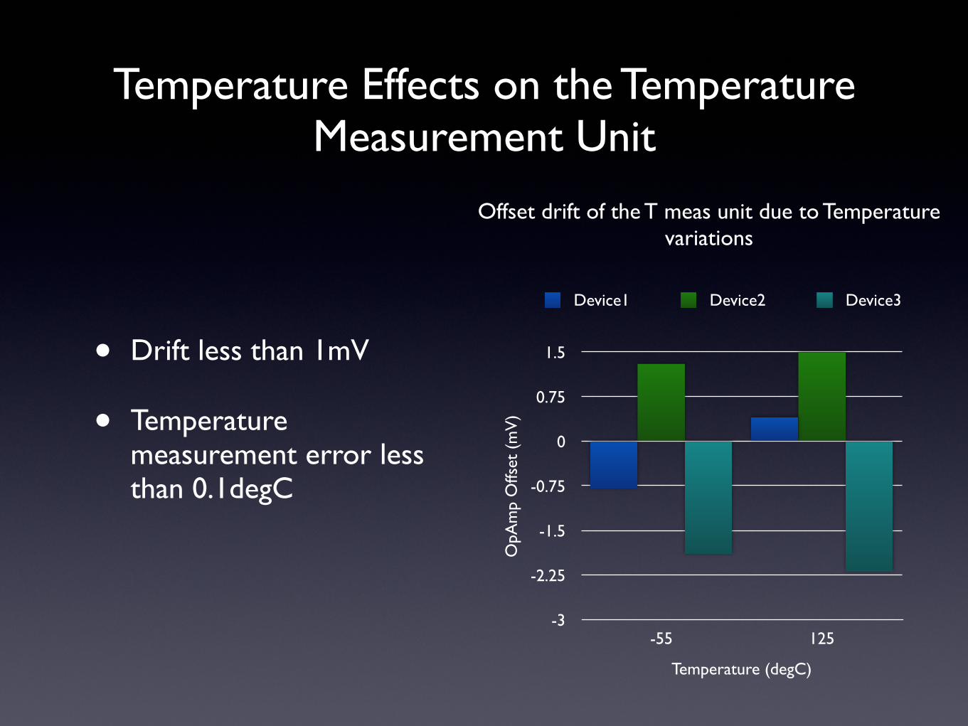
Temperature Effects on the Temperature Measurement Unit
• Drift less than 1mV
• Temperature measurement error less than 0.1degC
Offset drift of the T meas unit due to Temperature variations
-3
-2.25
-1.5
-0.75
0
0.75
1.5
-55 125
OpA
mp
Offs
et (
mV
)
Temperature (degC)
Device1 Device2 Device3
Temperature Measurement• Current Source offset (Pre and post Rad)• Anneal has no effects
• Current Source offset (Pre and post Rad)• Anneal has no effects
Temperature Measurement
Digital Sampler
• Level shifter and analog comparator
• Speed is adequate for 64MSPS operation
• Level shifter is a simple p type source follower
• Threshold can be adjusted through the bias voltage of the follower
Digital Sampler
Rbias=47KThreshold is adjusted through RbiasIf Din+ - Din- > THR then output is high
Power Supply Variation is ~50mV (acceptable)
Temperature Effects on the Digital Sampler
Digital Sampler
•Device to Device Variation for AS1145•Variation is 60mV•No Calibration Tables needed
TID Test Campaign
Digital Sampler threshold variation and 300 KRad
TID Test Campaign
Digital Sampler threshold variation and 1000 KRad
Leakage Currents
• Digital Leakage Current varies from device to device from 400 to 1500 nA
Ioff (pA/um)Ioff (pA/um)
Target Max
Nfet
Pfet
2.5 100
3.5 50
• Total W of nfets = 177 mm
• Total W of pfets = 531 mm
• Measurement in line with expected values
• ETM is nearly all NAND design (stacking effect factor is high)
• Multifinger layout topology in the drivers
Parameters from IHP
Leakage Currents
• Linear Dependency on power supply
Leakage Currents
• Temperature Dependency
• 25 to 125 degC:
• ~200x
Leakage CurrentSN018
SN019
SN020
SN021
SN022
SN023
SN024
SN025
SN026
SN027
SN028
SN029
SN030
SN031
SN032
SN033
SN034
SN035
SN036
SN037
0 0.50 1.00 1.50 2.00 2.50
0.99
1.24
0.69
0.78
1.05
1.02
1.12
1.02
0.80
0.69
0.98
0.81
1.33
2.14
0.87
1.02
0.83
1.43
0.75
ILeakage (uA)
AS1203SN001
SN002
SN003
SN004
SN005
SN006
SN007
SN008
SN009
SN010
SN011
SN012
SN013
SN014
SN015
SN016
SN017
0 0.50 1.00 1.50 2.00 2.50
0.77
0.47
0.83
1.39
0.97
0.50
0.48
0.62
0.70
0.53
0.48
0.68
0.56
0.40
1.20
Chart 7
ILeakage (uA)
AS1145
Leakage Current
Leakage Current
Leakage Current
0
1.00
2.00
3.00
4.00
5.00
6.00
7.00
Pre-Rad T0 (305K) T0+68 T0+160 T0+360
Leakage (uA) current at pre-RAD & various anneal steps
Ileak
age
(uA)
RLD01 RLD02 RLD03 RLD04 RLD05
0
2.00
4.00
6.00
8.00
T0 (305K) T0+68 T0+160 T0+360
Normalized leakage current at various anneal steps
Ileak
age
(Nor
mal
ized
to p
reRa
d)
RLD01 RLD02 RLD03 RLD04 RLD05
100degCRoom T 100
degCRoom T
At the end of the anneal process leakage currents fall to 1.7x their respective pre-rad value
Leakage Current
100degCRoom T 100
degCRoom T
At the end of the anneal process leakage currents fall to 2.5x their respective pre-rad value
0
1.00
2.00
3.00
4.00
5.00
6.00
7.00
8.00
Pre-Rad T0 (1040K) T0+124 T0+226 T0+394
Leakage (uA) current at pre-RAD & various anneal steps
Ileak
age
(uA)
RLD06 RLD07 RLD08 RLD09 RLD10
0
2.00
4.00
6.00
8.00
10.00
12.00
T0 (1040K) T0+124 T0+226 T0+394
Normalized leakage current at various anneal steps
Ileak
age
(Nor
mal
ized
to p
reRa
d)
RLD06 RLD07 RLD08 RLD09 RLD10
Leakage Current
SEE TestsSEU Cross Section
• No SELs up to 67 MeV-cm2/mg at 85 degC
• SEU cross section is at 57 MeV-cm2/mg for the nominal core power supply of 2.5V
• Falls down to 40 MeV-cm2/mg if power supply is reduced to 2.2V
• SEUs types are balanced
SEU Type Counts
0 to 1
1 to 0
195
203
Channel Mapping of SEUsSTD RTU
ETM1
FM ETM Yield
AS1145 As1203 Total
Failed Analog
Failed Digital
Low Performance
Good
3 2 5
2 3 5
0 2 2
12 13 25
Failed Analog14%
Failed Digital14%
Low Performance5%
Pass68%
Conclusions• ETM is a mixed signal
rad hard low power telemetry acquisition ASIC
• It can replace boards with discrete components for essential telemetry, RTU and instrument housekeeping applications