The Joint Test Action Group by Colin Maunder British Telecom Research Laboratories What is JTAG? JTAC — the Joint Test Action Croup — is an international group representing companies seeking solutions to the test problems in hybrid and PCB products which are being created by the combination of complex integrated circuits and surface-mount technology. The companies involved in the group are keenly aware of the extreme difficulty of using traditional techniques such as in-circuit testing for testing surface-mount products. These problems will eventually become evident throughout the digital electronics industry, and can only be solved satisfactorily by collaboration between integrated circuit users and those responsible for chip design. JTAG, which was established as a result of an initiative within Philips, currently includes representatives from: AT&T (USA) Bull Systemes (France) GEC (UK) Marconi (UK) Plessey (UK) British Telecom (UK) ElektronikCentralen (Denmark) ITT (Europe) Philips (Netherlands) Siemens (West Germany). The problem Over the years, the automatic test equipment used to test electronic products has evolved to cope with continued increases both in the number of integrated circuit packages used on, say, a printed circuit board and in the complexity of the integrated circuits themselves. Typically, manufacturers of assembled printed circuit boards will use high- pin-count in-circuit and functional board test systems, either separately or in sequence, to detect defects and Computer-Aided Engineering Journal August 1986 allow high quality levels to be achieved in their shipped products. Both these types of test equipment have increased in cost as IC complexities have increased and, further, both have difficulty in dealing with surface-mount technology — particularly in those cases where the increased component packing density achievable with the new technology is used to its full capability. For example, the cost of bed-of-nails test fixtures for surface-mount technology is high, and probing can be impossible where components are packed densely. It is clear that existing test technology will be faced by increasing difficulties as surface-mount technology continues to develop. The way forward therefore seems to be through the use of structured design techniques at the board level, rather than through continued evolution of existing test strategies. Boundary-scan Boundary-scan is a design structure which, if included in integrated circuit designs, solves some of the most severe problems in testing assembled surface-mount digital circuits. The technique involves the inclusion of a shift register latch adjacent to each component pin so that signals between chips can be controlled and observed using scan testing methods (see the panel). If the technique is applied in all the integrated circuits used to produce a product, the boundary-scan path which results can be used to test for the majority of the defects introduced by the assembly process (open circuits, solder splashes, wrongly inserted or incorrect components etc.). In effect, the boundary-scan path test can detect many of the faults which in-circuit testers are currently used to detect, but without the need for extensive bed-of-nails access and 121
Transcript
The Joint Test Action Groupby Colin MaunderBritish Telecom Research Laboratories
What is JTAG?
JTAC — the Joint Test Action Croup —is an international group representingcompanies seeking solutions to thetest problems in hybrid and PCBproducts which are being created bythe combination of complexintegrated circuits and surface-mounttechnology. The companies involvedin the group are keenly aware of theextreme difficulty of using traditionaltechniques such as in-circuit testingfor testing surface-mount products.These problems will eventuallybecome evident throughout the digitalelectronics industry, and can only besolved satisfactorily by collaborationbetween integrated circuit users andthose responsible for chip design.
JTAG, which was established as aresult of an initiative within Philips,currently includes representativesfrom:
Over the years, the automatic testequipment used to test electronicproducts has evolved to cope withcontinued increases both in thenumber of integrated circuit packagesused on, say, a printed circuit boardand in the complexity of theintegrated circuits themselves.Typically, manufacturers of assembledprinted circuit boards will use high-pin-count in-circuit and functionalboard test systems, either separatelyor in sequence, to detect defects and
Computer-Aided Engineering Journal August 1986
allow high quality levels to beachieved in their shipped products.
Both these types of test equipmenthave increased in cost as ICcomplexities have increased and,further, both have difficulty in dealingwith surface-mount technology —particularly in those cases where theincreased component packing densityachievable with the new technology isused to its full capability. For example,the cost of bed-of-nails test fixtures forsurface-mount technology is high, andprobing can be impossible wherecomponents are packed densely.
It is clear that existing testtechnology will be faced by increasingdifficulties as surface-mounttechnology continues to develop. Theway forward therefore seems to bethrough the use of structured designtechniques at the board level, ratherthan through continued evolution ofexisting test strategies.
Boundary-scan
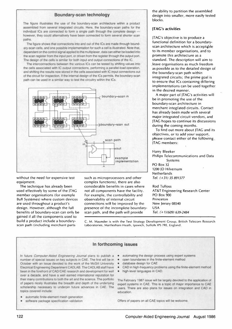
Boundary-scan is a design structurewhich, if included in integrated circuitdesigns, solves some of the mostsevere problems in testing assembledsurface-mount digital circuits. Thetechnique involves the inclusion of ashift register latch adjacent to eachcomponent pin so that signalsbetween chips can be controlled andobserved using scan testing methods(see the panel).
If the technique is applied in all theintegrated circuits used to produce aproduct, the boundary-scan pathwhich results can be used to test forthe majority of the defects introducedby the assembly process (opencircuits, solder splashes, wronglyinserted or incorrect componentsetc.). In effect, the boundary-scanpath test can detect many of the faultswhich in-circuit testers are currentlyused to detect, but without the needfor extensive bed-of-nails access and
121
Boundary-scan technology
The figure illustrates the use of the boundary-scan architecture within a productassembled from several integrated circuits. Here, the boundary-scan paths for theindividual ICs are connected .to form a single path through th;e complete design —however, they eould alternatively have been connected to f<brm? several shorter scanpaths. • ' " ' , • .' . ?••[. '. . •' •
The technique has already beenused effectively by some of the JTACmember organisations (for exampleBull Systemes) where custom devicesare used throughout a product'sdesign. However, although the fullbenefits of boundary-scan can only begained if all the components used tobuild a product include a boundary-scan path (including merchant parts
such as microprocessors and othercomplex functions), there are alsoconsiderable benefits in cases wherenot all components have the facility.For example, the controllability andobservability of internal circuitconnections will be improved by thepresence of the incomplete boundary-scan path, and the path will provide
the ability to partition the assembleddesign into smaller, more easily testedblocks.
JTAG's activities
JTAG's objective is to produce afunctional definition for a boundary-scan architecture which is acceptableto its member organisations, and topromote this architecture as astandard. The description will aim to
.leave organisations as much freedomas-possible as to the detailed design ofthe boundary-scan path withinintegrated circuits; the prime goal isto ensure that ICs containing differingimplementations can be used togetherin the desired manner.
A major part of JTAC's activities willbe in promoting the use of theboundary-scan architecture inmerchant integrated circuits. Contacthas already been made with severalmajor integrated circuit vendors, andJTAG hopes to continue its discussionsduring the coming months.
To find out more about JTAC and itsobjectives, or to add your support,please contact either of the following.JTAG members:
' • CAD in fnigh-f requehcy !p jdb)em^p js i | | i { ^ - j i | i te^J^^^^h i^Shigh-level languages in CAD.-- :~v-"" ' ' ' : ;T *, *;* •*'f"^',-^"'V; •5'£**?f'liin
vttm . . . . . . •. ' '- ' / ^^v. - * . •S.^'-"-.SiV*'1their-m'3ny/G0,ntr{bi$^^^ the-February 1987 issue will be*la*rg§fy/de"^te¥i " ' *of pape/r-s mieely jriii istfafct^ReAdth-a^d-depth of theunderl^ing: - exoe'rtWems in CAE. This-i's a t o m f i f i i l i i
e^t i s [ b i | l i ^ ) ^ i ^ | ^ artt aid the science T'he portfolio- ' t