+ All Categories
Home > Documents > The Meeting Book

The Meeting Book

Date post: 14-Feb-2017
Category:
Upload: ngominh
View: 219 times
Download: 0 times
Share this document with a friend
132
SIMFP 2016 The Fifth Saudi International Meeting on Frontiers of Physics Jazan University, Jazan, Saudi Arabia 16-18 February 2016 Meeting Book Organizers: University Vice-Presidency for Quality and Academic Development, Physics Department and Faculty of Science, @ Jazan University, Saudi Arabia. http://www.jazanu.edu.sa/SIMFP2016
Transcript

SIMFP 2016The Fifth Saudi International Meeting on Frontiers of PhysicsJazan University, Jazan, Saudi Arabia16-18 February 2016

Meeting Book

Organizers:

University Vice-Presidency for Quality and Academic Development,Physics Department and Faculty of Science,@ Jazan University, Saudi Arabia.

http://www.jazanu.edu.sa/SIMFP2016

SIM

FP20

16Th

eFi

fthS

audi

Inte

rnat

iona

lMee

ting

onFr

ontie

rsof

Phy

sics

Department of Physics, Faculty of Science, Jazan University.Gizan 22822 P.O. Box 114, Kingdom of Saudi Arabia.c©2016 SIMFP 2016 Committee, Jazan University, All rights reserved.

c© SIMFP 2016 Committee

Department of Physics,Jazan University,All rights reserved.

Printed in KSA.

SIMFP 2016

WelcomeRESPECTABLE COLLEAGUES, LADIES AND GENTLEMEN,ASSALAM ALAIKUM ,

It’s my great pleasure to welcome all of you to the Fifth Saudi Inter-national Meeting on Frontiers of Physics held at Jazan University inthe city of Jizan, Saudi Arabia, 16 -18 Feb 2016. We are delightedthat this meeting continues to attract many colleagues working at highlyrespected universities within theKingdom and by many scientistswho have traveled from famousinstitutions in distant lands. Onbehalf of Jazan University and theorganizing committee I welcome alldistinguished Speakers and Guests.We wholeheartedly thank you fortaking the time to inform us and toshare with other colleagues resultsfrom important projects you haveundertaken in several subfields ofphysics. I know we will all wantto warmly thank the many on our campus who have dedicated severalmonths on this splendid event, ranging from dedicated office staff, to theindefatigable Organizing Committee, and also including all other colleaguesand university workers, who made sure we could discuss physics andsocialize at this beautiful venue. It is with sincere gratitude that we thankActing Rector of Jazan University, Professor Dr. Mohammed bin Ali Rabiyaand all University vice Rectors for their constant support for this meeting.This year, our Saudi Meeting on Frontiers of Physics takes a further step toestablish itself as a leading scientific meeting in physics in Saudi Arabiaby publishing the meeting proceedings in collaboration with the renownedAmerican Institute for Physics (AIP) , where selected papers will be refereedand published by AIP ; we thank AIP for their interest in the SIMFP andsupport. We hope that such initiative will attract even more participants infuture SIMFP meetings and encourage further research activities.The SIMFP2016 program contains scientific activities as well as socialcomponents , I hope you enjoy the whole program and I wish you all a mostenjoyable stay in Jizan.

Professor Ali Al-Kamli, SIMFP2016 Chair and Vice Rector.

i

Contents SIMFP 2016

Contents

1 About the Workshop 1

2 Committees 3

3 Invited Speakers Biographies 5

4 Abstracts 154.1 The Invited Talks . . . . . . . . . . . . . . . . . . . . . . 174.2 Quantum Optics and Laser Physics . . . . . . . . . . . . 274.3 Photonics and Plasmonics . . . . . . . . . . . . . . . . . 374.4 Atomic and Molecular Physics . . . . . . . . . . . . . . 494.5 Quantum Information Science . . . . . . . . . . . . . . . 594.6 Materials Science . . . . . . . . . . . . . . . . . . . . . 654.7 Nuclear and Particle Physics . . . . . . . . . . . . . . . 894.8 Nanoscience and Engineering . . . . . . . . . . . . . . . 1014.9 Interdisciplinary Physics . . . . . . . . . . . . . . . . . . 113

5 The Social Program 121

iii

1 About the Workshop SIMFP 2016

About the WorkshopThe Fifth Saudi International Meeting on Frontiers of Physics 2016 aims tobring together researchers and scientists from Saudi Arabia and abroad to ex-change new ideas, share their experiences, discuss their latest achievements,and present their results in allaspects of new frontiers of physicswith particular emphasis oninterdisciplinary aspects. Themeeting is organized by theDepartment of Physics at JazanUniversity, Saudi Arabia, during16-18 February 2016, and it willbe held at the site of the newJazan University campus, in thecity of Gizan on the southerncoast of the Red Sea, 775 Kmsouth of Makkah. With the 2016Workshop, this annual event willbe in its Fifth edition to be addedto the previous workshops. Theprogram will include invited talks,oral and poster presentationsin a variety of research fieldsin physics, and also plenarytalks covering interdisciplinaryphysics.

Objectives

1. To provide an ideal platform to promote scientific dialogue and dis-cussions on current directions in modern physics.

2. To open a venue for future cooperation and joint research betweenJazan University and other high profile institutions.

1

SIMFP 2016 1 About the Workshop

Topics

Quantum Optics and Laser PhysicsPhotonics and PlasmonicsAtomic and Molecular PhysicsQuantum Information ScienceMaterials SciencesNuclear and Particle PhysicsNanoscience and EngineeringInterdisciplinary Physics

Conference Organization

Organized by

University Vice-Presidency for Quality and Academic Development,Physics Department and Faculty of Science,@ Jazan University, Saudi Arabia.

2

2 Committees SIMFP 2016

Committees

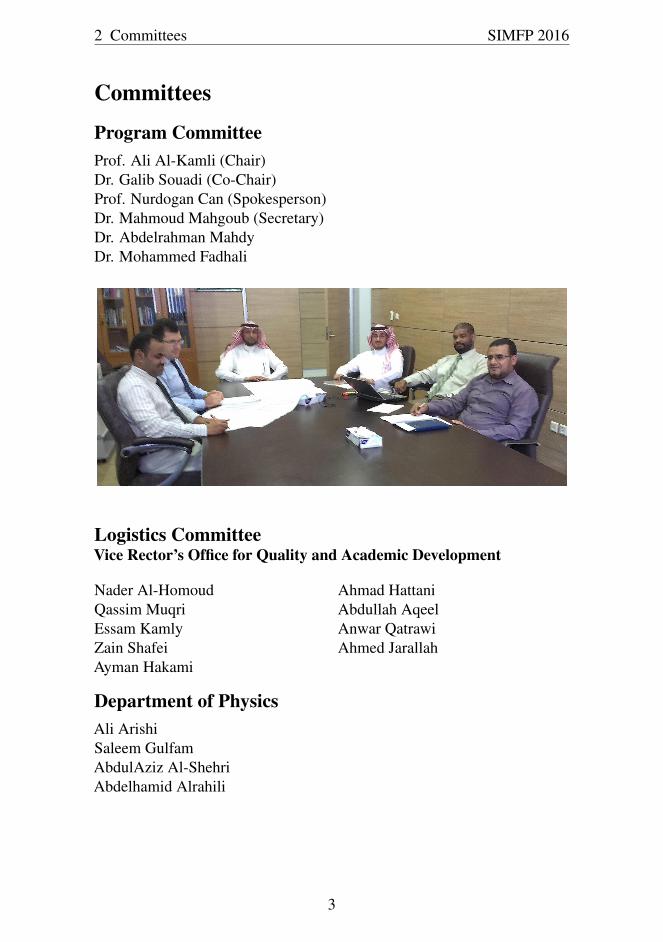
Program CommitteeProf. Ali Al-Kamli (Chair)Dr. Galib Souadi (Co-Chair)Prof. Nurdogan Can (Spokesperson)Dr. Mahmoud Mahgoub (Secretary)Dr. Abdelrahman MahdyDr. Mohammed Fadhali

Logistics CommitteeVice Rector’s Office for Quality and Academic Development

Nader Al-HomoudQassim MuqriEssam KamlyZain ShafeiAyman Hakami

Ahmad HattaniAbdullah AqeelAnwar QatrawiAhmed Jarallah

Department of PhysicsAli ArishiSaleem GulfamAbdulAziz Al-ShehriAbdelhamid Alrahili

3

3 Invited Speakers Biographies SIMFP 2016

Invited Speakers Biographies

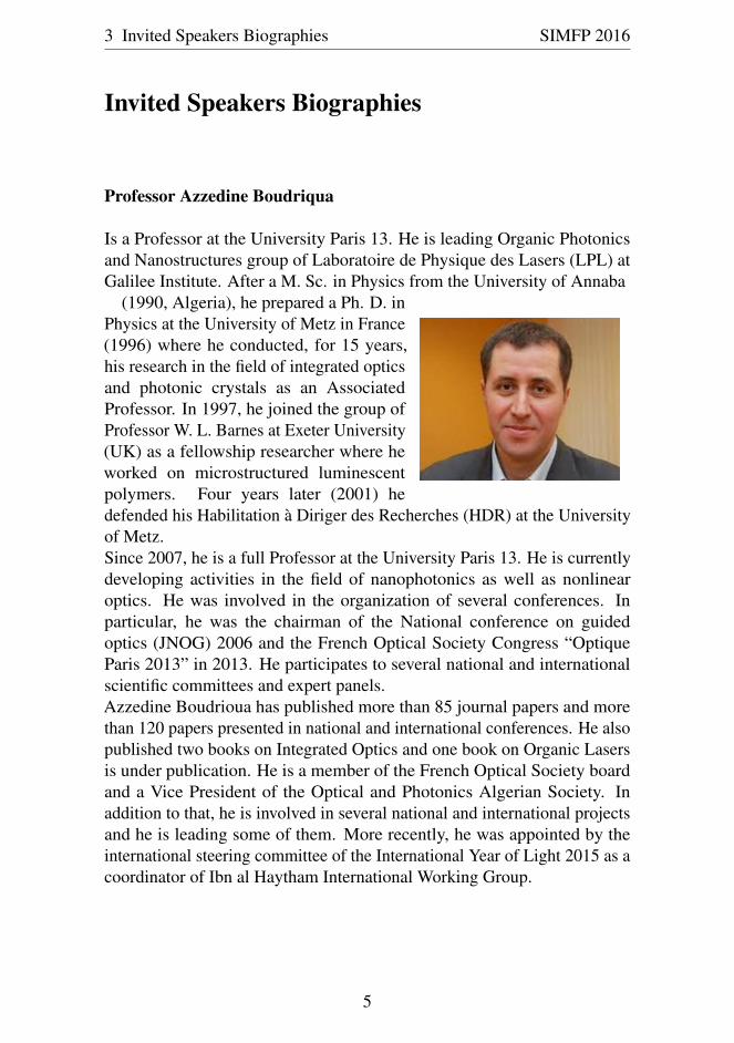
Professor Azzedine Boudriqua

Is a Professor at the University Paris 13. He is leading Organic Photonicsand Nanostructures group of Laboratoire de Physique des Lasers (LPL) atGalilee Institute. After a M. Sc. in Physics from the University of Annaba

(1990, Algeria), he prepared a Ph. D. inPhysics at the University of Metz in France(1996) where he conducted, for 15 years,his research in the field of integrated opticsand photonic crystals as an AssociatedProfessor. In 1997, he joined the group ofProfessor W. L. Barnes at Exeter University(UK) as a fellowship researcher where heworked on microstructured luminescentpolymers. Four years later (2001) hedefended his Habilitation à Diriger des Recherches (HDR) at the Universityof Metz.Since 2007, he is a full Professor at the University Paris 13. He is currentlydeveloping activities in the field of nanophotonics as well as nonlinearoptics. He was involved in the organization of several conferences. Inparticular, he was the chairman of the National conference on guidedoptics (JNOG) 2006 and the French Optical Society Congress “OptiqueParis 2013” in 2013. He participates to several national and internationalscientific committees and expert panels.Azzedine Boudrioua has published more than 85 journal papers and morethan 120 papers presented in national and international conferences. He alsopublished two books on Integrated Optics and one book on Organic Lasersis under publication. He is a member of the French Optical Society boardand a Vice President of the Optical and Photonics Algerian Society. Inaddition to that, he is involved in several national and international projectsand he is leading some of them. More recently, he was appointed by theinternational steering committee of the International Year of Light 2015 as acoordinator of Ibn al Haytham International Working Group.

5

SIMFP 2016 3 Invited Speakers Biographies

Dr. S. Sasi Florence

Dr.Sasi Florence is an Assistant Professor in the Department of Physics,College of Science in Al-Ardha at Jazan University, Saudi Arabia. Sheearned her Ph.D from Mother Teresa Women’s University, India. Herresearch interests focus on II-VI nano semiconductors, Organic LigandCapped Nano semiconductors, Nano lithography for Solar Cell Applications.She has over 17 peer reviewed International journals, participated andpresented over 20 International conferences and workshops. She hasreceived and successfully completed a prestigious Women Scientist ProjectScheme-A (2011-2014) funded by the Department of Science & Technology(DST), Central Government of India. She has been served as an Organizingcommittee member in the International conferences held at Mother TeresaWomen’s University, India. She has attended several training coursesand workshops by the Government of India including Women ScientistsScheme-A awardees program, Hyderabad and Training Program in Science& Technology for Rural Societies, LBSNAA, Mussoorie, India. She haspresented her research articles in Nanotoday event at Singapore and GordonResearch Conference at United States of America. Her recent researchproject has been accepted by the Deanship of Scientific Research, JazanUniversity, Jizan, Saudi Arabia.

6

3 Invited Speakers Biographies SIMFP 2016

Professor Javier Garcia Guinea

A Spanish geologist; born in Madrid; gradudated in the Universidad Com-plutense of Madrid (B.A., 1976); Ph.D. in Science University of Zaragoza,1981. He taught at the Spanish Universities of Extremadura, Zaragoza,and Madrid, from 1978 until his appointment in 1987 as Researcher of theMuseo Nacional de Ciencias Naturales (MNCN), an Institute of the SpanishResearching Council (CSIC).

His early work was concerned withgeology of Spanish ore deposits of gem-stones, mineralogy, and gemology. Helater contributed to the modernizationof the historical mineralogical collectionby setting and computing, to severalrearrangements of the minerals exhibitionhalls, and to the improvements of the ge-ological laboratories of the MNCN. Duringthe 1990s, Garcia-Guinea was visitingprofessor in the department of Optoelectronics and Thermoluminescence ofthe School of Physics of the University of Sussex conducting basic researchon thermoluminescence emissions of feldspar and carbonate minerals.Now, he is a professor of research CSIC at the MNCN institution for basicmineralogical research in the Department of Geology and for scientificmanagement of 7 persons in the following units: (i) laboratory of electronmicroscopy and spectroscopy facilities; (ii) geological laboratories; and (iii)historical collections of minerals, rocks, gemstones, and meteorites of theMNCN institution. Garcia-Guinea, J. has 190 hits in the Web of Science orScopus (ID:7003954168) including 162 co-authors of 23 different countries.In addition, Prof. Garcia-Guinea has 106 additional secondary documentsin divulgation journals, 140 presentations to meetings, 16 chapters of books,two patents, and five International Cooperation actions in Uruguay, Bolivia,Argentina, Ecuador and Vietnam. The last projects concerned research onspeleothems of the Ha Long Bay (Vietnam); Castañar de Ibor Cave (Spain);Carbonate phases with activators to model luminescence emissions of thecarbonates group and Thallium microscopic distribution and speciation inhydrothermal polymetallic mineralization areas and mine contaminatedsoils.

7

SIMFP 2016 3 Invited Speakers Biographies

Professor Dariusz Hreniak

Born in 1976 in Wroclaw (Poland). Doctor of chemistry at the Insti-tute of Low Temperature and Structure Research Polish Academy of Sci-ences in Wroclaw. Since 2005, Director’s Proxy for Implementations.Present research activity are laser spec-troscopy, nanocrystals syntheses, sol-gelmaterials, rare-earth elements, luminescentmarkers, nanoceramic processing and char-acterization and luminescence properties ofthe rare-earth ions in glasses, nanoceramicsand nanocomposites.CEO in spin-off type companies: Nanovec-tors Sp. z o.o. (since 2011, optical securingof valuable objects) and in Ipanterm Sp. zo.o. (since 2013, new fire-proof insulating materials). Published more than120 publications in international journals and book chapters (h-index 23,>1700 total citations) and 16 patents and patents pending.

8

3 Invited Speakers Biographies SIMFP 2016

Dr. Khai Le

Was born in Khanh Hoa, Vietnam, in 1983. He received a BSc degree inPhysics from University of Natural Sciences at Ho Chi Minh city, VietnamNational University, Vietnam, in 2005. From 2006 to 2008, he was withthe Nanophotonics group at the Department of Electrical and ComputerEngineering, Ajou University, Korea.

In 2008, he was awarded the BOF doctoralscholarship to study Electrical Engineering(Photonics) in the Photonics ResearchGroup at the Department of InformationTechnology (INTEC), Ghent University,Belgium where he received the PhD degreeon June 2011. During his PhD studyhe has spent 3 months at George GreenInstitute for Electromagnetics Research,University of Nottingham, Nottingham,UK as a visiting scholar to perform the short term scientific mission(STSM) program of COST Action MP0702. From July 2011 to Oct. 2013,he worked at the University of Texas at Austin, USA and University ofToronto, Canada as a postdoctoral fellow. On Nov. 2013 he joined inHoa Sen University, Vietnam and acted as Dean of Faculty of Science andTechnology. From May 2014 to May 2015, he took a sabbatical leave forUniversity of Minnesota, Duluth, MN, USA as a visiting professor forteaching and research. From Oct. 2015, he has been a visiting professor inPhysics Department, Jazan University, KSA for two months.He has research interests in design, modeling, fabrication and charac-terization of nanophotonic devices. He serves as an active reviewerfor international journals including IEEE/OSA Journal of LightwaveTechnology, IEEE Photonics Technology Letters, Journal of Optical Societyof America A (and B), Optics Express, Optics Letter, Applied Optics,Plasmonics.

9

SIMFP 2016 3 Invited Speakers Biographies

Professor Younes Messaddeq

Younès Messaddeq holds a PhD in chemistry and a bachelor’s degree insolid state chemistry from the Universite de Rennes 1, France. He is theChairholder of the prestigious Canada’s Excellence Research Chair (CERC)in Enabling Photonic Innovations for Information and Communications witha budget of 28M$ over a period of seven years. He is currently leading ateam of 44 researchers (graduate students, post-doctoral fellow, technicians,and research professionals). He is one of the world’s most accomplishedresearchers in glass-based materials and optical fiber development. His R&Dactivities include advanced glass-based materials, production of specialtyoptical fibers, preparation and characterization of hybrid materials using thesol-gel process and preparation of nanostructured materials.

He has received several distinctions andawards, including Special Optical FibersAward for Telecommunication from Mairof Araraquara in Brazil, STA fellowship onOptical Fibers from the Japanese Ministerof Science and Technology, Heraeus DentalAward on Dental composites, Ruy FerreiraSanto Award and 1A classification fromthe Minister of Science and Technologyand CNPq(National Consul of Research) –Brazil. He is a member of several committees (Editorial Board –Journal ofNon crystalline Solids(JNCS),Member – NSF/International Materials Insti-tute for New Functionality in Glass, International Non-Oxide Committee(ISNOG), International Glass Committee (IGC).He published more than 365 papers in refereed journals (5300 citation,h-index=37) and presented several invited talks (36 over the last 6 years).He currently holds 20 patents, 7 of which were submitted after his arrivalat Université Laval (since 2011). He contributed to the creation of threespinoffs companies in Brazil (Terra Azul, Microtube, DMC-Biocel). In2013, he was appointed the director of the Joint International Research Unitbetween Universidade Estadual Paulista (UNESP)-Ulaval (Brazil-Canada)for a period of five years. In 2015, he established the joined researchlaboratory between University of Bordeaux in France and Laval University.

10

3 Invited Speakers Biographies SIMFP 2016

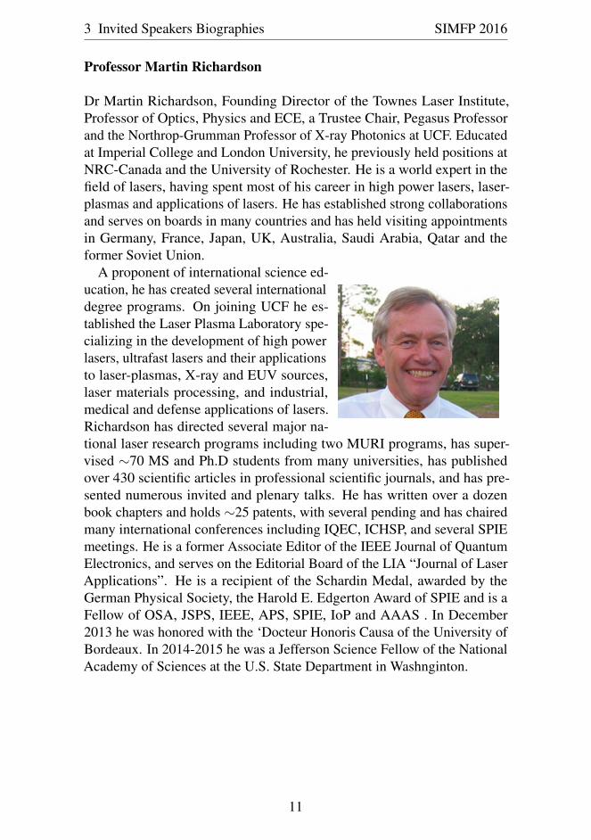
Professor Martin Richardson

Dr Martin Richardson, Founding Director of the Townes Laser Institute,Professor of Optics, Physics and ECE, a Trustee Chair, Pegasus Professorand the Northrop-Grumman Professor of X-ray Photonics at UCF. Educatedat Imperial College and London University, he previously held positions atNRC-Canada and the University of Rochester. He is a world expert in thefield of lasers, having spent most of his career in high power lasers, laser-plasmas and applications of lasers. He has established strong collaborationsand serves on boards in many countries and has held visiting appointmentsin Germany, France, Japan, UK, Australia, Saudi Arabia, Qatar and theformer Soviet Union.

A proponent of international science ed-ucation, he has created several internationaldegree programs. On joining UCF he es-tablished the Laser Plasma Laboratory spe-cializing in the development of high powerlasers, ultrafast lasers and their applicationsto laser-plasmas, X-ray and EUV sources,laser materials processing, and industrial,medical and defense applications of lasers.Richardson has directed several major na-tional laser research programs including two MURI programs, has super-vised ∼70 MS and Ph.D students from many universities, has publishedover 430 scientific articles in professional scientific journals, and has pre-sented numerous invited and plenary talks. He has written over a dozenbook chapters and holds ∼25 patents, with several pending and has chairedmany international conferences including IQEC, ICHSP, and several SPIEmeetings. He is a former Associate Editor of the IEEE Journal of QuantumElectronics, and serves on the Editorial Board of the LIA “Journal of LaserApplications”. He is a recipient of the Schardin Medal, awarded by theGerman Physical Society, the Harold E. Edgerton Award of SPIE and is aFellow of OSA, JSPS, IEEE, APS, SPIE, IoP and AAAS . In December2013 he was honored with the ‘Docteur Honoris Causa of the University ofBordeaux. In 2014-2015 he was a Jefferson Science Fellow of the NationalAcademy of Sciences at the U.S. State Department in Washnginton.

11

SIMFP 2016 3 Invited Speakers Biographies

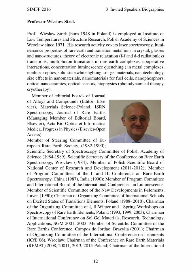
Professor Wieslaw Strek

Prof. Wiesław Strek (born 1948 in Poland) is employed at Institute ofLow Temperatures and Structure Research, Polish Academy of Sciences inWroclaw since 1971. His research activity covers laser spectroscopy, lumi-nescence properties of rare earth and transition metal ions in crystal, glassesand nanostructures, theory of electronic relaxation (f-f and d-d radiationlesstransitions, multiphoton transitions in rare earth complexes, cooperativeinteractions, concentration luminescence quenching ) in metal complexes,nonlinear optics, solid state white lighting, sol-gel materials, nanotechnology,size effects in nanomaterials, nanomaterials for fuel cells, nanophosphors,optical nanoceramics, optical sensors, biophysics (photodynamical therapy,cryotherapy).

Member of editorial boards of Journalof Alloys and Compounds (Editor- Else-vier), Materials Science-Poland, ISRNSpectroscopy, Journal of Rare Earths(Managing Member of Editorial Board,Elsevier), Acta Bio-Optica et InformaticaMedica, Progress in Physics (Elsevier-OpenAccess)Member of Steering Committee of Eu-ropean Rare Earth Society, (1982-1990);Scientific Secretary of Spectroscopy Committee of Polish Academy ofScience (1984-1989), Scientific Secretary of the Conference on Rare EarthSpectroscopy, Wroclaw (1984); Member of Polish Scientific Board ofNational Center of Research and Development (2011-2012); Memberof Program Committees of the II and III Conference on Rare EarthSpectroscopy, China (1987), India (1990); Member of Program Committeeand International Board of the International Conferences on Luminescence,Member of Scientific Committee of the New Developments in f-elements,Luven (1990); Chairman of Organizing Committee of International Schoolson Excited States of Transitions Elements, Poland (1988- 2010); Chairmanof the Organizing Committee of I, II Winter and I Spring Workshops onSpectroscopy of Rare Earth Elements, Poland (1993, 1999, 2003); Chairmanof International Conference on Sol Gel Materials, Research, Technology,Applications, SGM 2001, 2003; Member of Scientific Committee of theRare Earths Conference, Campos do Jordao, Brazylia (2001); Chairmanof Organizing Committee of the International Conference on f-elements(ICfE’06), Wroclaw; Chairman of the Conference on Rare Earth Materials(REMAT) 2008, 20011, 2013, 2015-Poland; Chairman of the International

12

3 Invited Speakers Biographies SIMFP 2016

Board of International Confrence on Luminescence 2014. Co-Chairman ofLaser Ceramic Symposium 2004-2015.Supervisor of 9 doctor thesis.Author/co-author of more than 400 papers, more than 4000 citations, Hirschindex-35. Author more than 30 patents in optical security, nanotechnology,laser therapy, cryotherapy, sol-gel technology, thermal insulation porousmaterials.Visiting professor at institutes and universities in France, Denmark, Brasil,Germany, Belarus, Russia, Italy, Finland.Editor and co-editor of conference proceedings: „Rare Earth Spectroscopy”,Eds. B. Jezowska-Trzebiatowska, J. Legendziewicz, W. Strek (WorldSci. Publ., Singapore, 1985), „Photon Emission In Biological Systems”,Eds. B. Jezowska-Trzebiatowska , J. Sławinski, B. Kochel, W. Strek(World Sci. Press, Singapore, 1987), „Biological Luminescence”, Eds.B. Jezowska-Trzebiatowska, J. Sławinski, B. Kochel, W. Strek (WorldSci.Press, Singapore, 1990); „Excited States of Transition Elements”, B.Jezowska- Trzebiatowska, J. Legendziewicz, W. Strek (World Sci. Press,Singapore,1988, 1992, 1995, 1998, 2001), Optical Materials 2003, 2006,2008, 2012).

13

4 Abstracts SIMFP 2016

Abstracts

15

SIMFP 2016

The Fifth Saudi International Meeting on Frontiers of Physicswww.jazanu.edu.sa/SIMFP2016

4.1 The Invited Talks

Surface plasmon-enhanced emission in an

organic light-emitting diode: toward organic

laser diode under electrical pumping

Azzedine Boudrioua, Mahmoud Chakaroun, Alexis Fishcer

Université Paris 13, France

Organic laser diode (OLD) under electrical pumping is one of the most

challenging issues of organic optoelectronic filed. Despite the progress

made in recent years, the OLD is still not demonstrated. This is

particularly due to the intrinsic properties of organic compounds which

suffer from strong absorptions (polaronic, annihilation singlet-triplet, etc.)

as well as low electrical performances (low charge motilities, low current

density, etc.). In this context, most of works were concentrated on the

optical pumping and the optimization of the laser micro-cavity. The latter

can be either planar as defects in 2D photonic crystals or vertical

(commonly called VECSEL). Even if some works have demonstrated the

possibility of achieving optically-pumped micro or nano cavity organic

lasers having a high quality factor, the performances obtained are still

insufficient to consider the electrical pumping of these structures. At this

point of the OLD endeavor, several fundamental questions remain: by

using a reasonable current density, is it possible to enhance the produced

light (the rate of radiation) to reach the laser threshold without

deteriorating the organic medium? How can we do that?

In this proposal, we aim to increase the emission of the available organic

materials thanks to localized surface plasmon enhanced emission by using

metallic nanoparticles, and to investigate this effect in a micro-cavity for

laser effect improvement.

Submitting author: B., Azzedine, Université Paris 13, Laboratoire de

Physique des Lasers, UMR CNRS 7538, Université Paris 13, 93430

Villetaneuse, France, E-mail: [email protected].

SIMFP 2016 4 Abstracts

18

Large scale ZnTe nanostructures on polymer

micro patterns via capillary flow

S.Sasi Florence1, Nurdogan Can

1, Priyanka Sachan

2, Raju Kumar Gupta

2,

Hajer Adam1 and M.Umadevi

3

1Jazan University, Saudi Arabia,

2Indian Institute of Technology and

3Mother Teresa Women’s University, India

A novel approach to prepare micro patterns ZnTe nanostructures on Si

(100) substrate using thermal evaporation is proposed by capillary Flow

Lithography technique on a self-assembled sacrificial Polystyrene mask.

Polystyrene thin films on Si substrates are used to fabricate surface micro-

relief patterns. The deposited ZnTe nanoparticles properties were assessed

by X-ray diffraction, Atomic Force Microscope (AFM), Scanning

Electron Microscope (SEM), Raman spectroscopy, Photoluminescence

and UV-Vis spectrophotometry. The X-ray diffraction patterns of the films

exhibited reflection corresponding to the cubic (111) phase and showed

polycrystallinity with a Zinc blende structure. The SEM images indicated

that the particles were well dispersed and spherical in shape. We report

and demonstrate the micro-arrays of ZnTe nanoparticles on a self-

assembled sacrificial PS mask using a capillary flow photolithography

process which showed excellent structural, morphological and optical

properties which can be used in photovoltaic devices.

Submitting author: S.Sasi Florence, Jazan University, Faculty of Science

and Arts in Al-Ardha, Department of Physics, P. O. Box 114, Gizan

45142, Saudi Arabia.

E-mail: [email protected].

4 Abstracts SIMFP 2016

19

New strategies to optimize material analyses

using modern microscopes (ESEM, 3DWLI)

Javier Garcia-Guinea, Fernando Garrido, Paula Lopez-Arce, P., Laura

Tormo, Alberto Jorge, Marta Furio, Cristina Paradela.

1Museo Nacional Ciencias Naturales (MNCN-CSIC), Spain

There are numerous factors that can affect the decision of choosing the

most appropriate analytical technique. In many cases more than one

technique maybe applied, and trade-offs, such as improved spatial

resolution versus lower concentration sensitivity, are involved. Other

factors are analytical sampling depth; samples conduction; elemental

versus molecular chemical analyses; destructive versus non-destructive

techniques; survey versus specific element analysis; quantitative versus

qualitative results, etc. After a decade working with electronic and optical

microscopes coupled to elemental-chemical probes (EDS, WDS) and

spectral detectors (CL, PL, FL, Raman) we actually are circumventing the

traditional polarizing optical microscopes since the sample preparation

processes destroy large sample textures, introducing contaminant

abrasives and glues using dangerous and expensive consumables.

Alternatively, the modern large chambers of microscopes ESEM-EDS-

WDS-CL, Raman-PL and 3DWLI admit large specimens, e.g. 10x10x2

cm keeping textures and structures. In addition, to prepare these new large

sections we suggest extracting powdered samples to be used in XRD,

DTA-TG, FTIR, TL and DSC techniques and fresh little surfaces (chips)

using tongs to avoid contaminants to be also studied under the

microscopes. Our new 3D-White-Light-Interferometer optical microscope

(3DWLI) combine interferometry and confocal on one stand, offering

phase shifting and white light interferometry for characterization of very

smooth surfaces (<1 nm in roughness). This new optical microscope

provides novel interferometric and confocal colored images useful for

crystallographic measurements avoiding painful sample preparations as

those required by the ancient polarizing microscopes.

Submitting author: J. Garcia-Guinea. Museo Nacional Ciencias

Naturales (MNCN, CSIC). P. O. Box. Calle Jose Gutierrez Abascal 2.

Madrid, Spain. 28006. Tel +0034-639177997.

Email: [email protected]

SIMFP 2016 4 Abstracts

20

Synthesis, spectroscopic properties and possible

applications of rare-earth doped Sr2CeO4

nanomaterials

Mariusz Stefański, Robert Tomala, Łukasz Marciniak, Wiesław Stręk,

Dariusz Hreniak

Polish Academy of Sciences, Poland

Nanocrystalline powders of the Sr2CeO4 and Sr2CeO4 doped with rare-

earth ions were prepared using the modified Pechini’s method [1]. Their

morphology and structural and optical properties were studied. In

particular, the absorption, excitation and emission spectra, and emission

decays were recorded in a wide temperature range and analysed in details.

The quantum efficiencies for investigated samples were determined. It

was found that with increase of grain sizes the luminescence lifetime

significantly decreased. Strong thermal quenching of luminescence of

doped Sr2CeO4 nanocrystals was also noticed. The Sr2CeO4 nanoceramics

were also produced from the nanocrystalline powders by using high

pressure-low temperature (HPLT) isostatic sintering [2]. Possibility of

using Sr2CeO4 nanomaterials for lightning, optical thermometry and in

solar applications is discussed.

Submitting author: D. Hreniak, Institute of Low Temperature and

Structure Research, Polish Academy of Sciences, Wroclaw, Poland,

Poland, Tel: +48 71-39-54;

E-mail: [email protected].

References

[1] M. Stefański, L. Marciniak, D. Hreniak, W. Strek, Journal of

Physical Chemistry, 142, 184701 (2015).

[2] R. Fedyk, D. Hreniak, W. Łojkowski, W. Strek, H. Matysiak,

E. Grzanka, S. Gierlotka, P. Mazur, Optical Materials, 29, 1252-

1257 (2007).

4 Abstracts SIMFP 2016

21

Plasmonic and dielectric resonant structures for

light-trapping enhancement in organic solar cells

Khai Q. Le1,2

1Hoa Sen University, Vietnam and

2Jazan University, Saudi Arabia

Photovoltaic (PV) research has been attempting to find cheaper and more

manufacturable solar cells. Thin-film OSCs have potentially provided

such a route because of their lower cost in production and increased

manufacturing volume. This route is hampered by the need to achieve

higher efficiencies in OSC before becoming a viable solution. A primary

difficulty in achieving higher efficiencies is getting enough light to be

absorbed in the thin-film and the short diffusion length of carriers.

Thicknesses of organic solar cells are restricted by physical limitation

because of the need to utilize electrical characteristics of the material. If

the active material becomes too thick, it will result in significant reduction

in exciton collection from recombination within the active material.

Incident light propagates through the active material before enough can be

converted to excitons, due to the thickness restraint. On the other hand,

too thick active material beyond carrier diffusion length will cause current

loss due to recombination. Thus, the tradeoff between enough absorption

and minimizing recombination is the key issue in designing solar cells.

Failure to absorb photons within the absorption band or below the

bandgap of the polymer active layer limits the power conversion

efficiency of the OSC. A significant portion of all available sunlight is

unharvested due to either the reflection from the reflective electrodes of

the OSC or the transmission through the semitransparent active substrate.

In this talk, engineering plasmonic and dielectric resonant structures to

enhance light absorption in OSCs will be discussed. Physics insights the

enhancement will be explored and demonstrated.

Submitting author: K. Q., Lee, Hoa Sen University, Faculty of Science

and Technology, Hoa Sen University, Ho Chi Minh, Vietnam; Jazan

University, Faculty of Science, Department of Physics, Saudi Arabia.

E-mail: [email protected]

SIMFP 2016 4 Abstracts

22

Advances in special optical fibers

Younes Messaddeq

Université Laval, Québec, Canada

The main issues and greatest challenges for the development of new

photonic glasses materials and optical fibers are related to several aspects,

from their synthesis to their shaping and integration into photonic

devices. New drivers have arisen in recent years for the exploration and

development of new technologies related to glass science: i) the

photonic band- gap effect, ii) the production of nanostructured

materials and iii) the incorporation of nanoparticles in glass matrix.

Based on these aspects, we will discuss on the development of novel

optical glasses based on silica and heavy oxide and chalcogenide glasses

and their impact on various fields of application such as information

technology, environmental monitoring, biomedical devices and

security/defense.

I will present also, novel textile fabrics integrating unobtrusive multi-

material fibers that communicate through 2.4 GHz wireless networks with

excellent signal quality. The conductor elements of the textiles are

embedded within the fibers themselves, providing electrical and

chemical shielding against the environment, while preserving the

mechanical and cosmetic properties of the garments. These multi-

material fibers combine insulating and conducting materials into a well-

defined geometry, and represent a cost-effective and minimally- invasive

approach to sensor fabrics and bio-sensing textiles connected in real time

to mobile communications infrastructures.

Submitting author: Y. Messaddeq, Centre d’optique, photonique et

laser (COPL), Université Laval, Québec, Canada,

E-mail: [email protected]

4 Abstracts SIMFP 2016

23

The Mysteries of Ultrafast Laser Filamentation

in Air

Martin Richardson

University of Central Florida, USA

Laser light filamentation, first observed in the atmosphere two decades

ago continues to intrigue physicists across the globe. Its most visible

characteristic is the apparent ability of high intensity light beams to defy

the laws of diffraction, or the divergence of a propagating light, and

instead collapse on themselves into a self-sustaining light filaments stable

for 100’s meters. They pack intensities of > 10 13

W/cm2, high enough to

ablate most surfaces. Their mechanism of formation leads to the fact that

their peak intensity is uniquely clamped, providing a stable shot-to-shot

intensity beam with well-characterized profile. This enables Laser

induced breakdown spectroscopy (LIBS) of remote surface contaminants

at significant distances. Filaments emit white light in the forward and

backward directions, providing unique sources for remote absorption

spectroscopic sensing. Studies of filamentation are entering a new phase of investigation. As we

consolidate more our understanding of the dynamics of the creation and

propagation of single stabilized filaments in air, we can begin to deploy

new modalities in filamentation. In this review we consider our current

understand of single filament formation in air by conventional high

intensity femtosecond lasers, describing in particular new investigations

of the continuum emission and the impact molecular alignment can have

on filament propagation. We describe the use of multiple filaments to both

investigate the phase characteristics of filaments, and through multi-color

filaments to generate remote coherent THz emission. By manipulating the

initial phase of the originating laser beam, we describe how multiple

organized arrays of filaments can be generated, and illustrate this with the

recent demonstration of double helical rotating filaments. Structured

arrays of filaments open the pathway to many air filament scenarios,

including the guiding and manipulation of microwaves, and potentially

electric discharges.

Submitting author: M. Richardson, Townes Laser Institute, College of

Optics & Photonics, University of Central Florida, USA,

E-mail: [email protected]

SIMFP 2016 4 Abstracts

24

Laser induced white light emission in rare earth

doped nanocrystals

Wiesław Stręk, Łukasz Marciniak, Robert Tomala, Mariusz Stefański,

Artur Bednarkiewicz, Dariusz Hreniak

Polish Academy of Sciences, Poland

Laser induced white emission (LIWE) of rare earth doped nanocrystalline

powders is a subject of increasing research activity in last few years [1,2].

It was demonstrated that it is the broadband anti-Stokes emission

characterized by several characteristic features:

The intensity of LIWE depends on excitation power P of infrared CW

laser according to the power law of multiphoton absorption I ∝ PN, where

the order parameter N is a number of absorbed photons;

The LIWE intensity strongly depends on concentration of active ions and

on the atmosphere pressure and is the highest in vacuum, sometimes

being even 2-3 orders of magnitudes higher than in ambient atmosphere;

The LIWE intensity decreased with lowering the temperature of sample

and is accompanied by an efficient photocurrent;

The temperature of LIWE is relatively lower, much less than could be

predicted assuming incandescence - black body emission;

The LIWE occurs after enhancement above the power density threshold

and is characterized by long rise and decay times;

The LIWE is very efficient reaching even 10% of quantum yield.

The results of LIWE measurements are presented for several

nanocrystalline hosts (YAG, YAlO3, Sr2CeO4, LiYF4) doped with Nd3+

and Yb3+

ions. The mechanism of LIWE is discussed in terms of

intervalence charge transfer (IVCT) transitions.

Submitting author: W. Stręk, Institute of Low Temperature and Structure

Research, Polish Academy of Sciences, Wroclaw, Poland,

E-mail: [email protected].

References

[1] W. Strek, L. Marciniak, A. Bednarkiewicz, A. Lukowiak, R.

Wiglusz, D. Hreniak, Optics Express, 19, 14083-14092 (2011).

[2] W. Strek, L. Marciniak, P. Gluchowski, D. Hreniak, Optical

Materials, 35, 2013-2017 (2013).

4 Abstracts SIMFP 2016

25

SIMFP 2016

The Fifth Saudi International Meeting on Frontiers of Physicswww.jazanu.edu.sa/SIMFP2016

4.2 Quantum Optics and Laser Physics

Excitation mechanisms in a Hollow Cathode

Metal Vapor Laser (He-Cd+)

R. Periasamy

American University of Iraq, Sulaimani, Iraq

Metal vapor lasers (He-Cd+) operating in the negative flow region of a

low pressure gas discharge is to be presented. The operation conditions

and parametric studies of the laser will be discussed. The general

excitation processes in this design of hollow cathode has been studied by

emission spectroscopy [2]. The study gives the reasons for the negative

glow region of the discharge favoring all laser transitions. He-Cd+ laser

were able to operate in continuous mode giving seven laser transitions

simultaneously [1]. The seven transitions range from two in NIR, Red

and two green and one in blue and another in UV region.

The major excitation mechanisms for the blue and UV lines are expected

to be due to electron impact excitations but at high discharge currents

increases the population of the (He 23S) helium meta stables which are the

pump species of blue and UV transitions. The excitation mechanisms for

the infrared and red lines are by charge transfer and for the two green

lines it is partly by Penning and partly by radiative cascading. The

electron energy distribution in a hollow cathode discharge is very highly

non-Maxwellian and varies dramatically with discharge current, buffer

gas pressure and radial position of a hollow cathode. The laser light

coming out of the brewster angle cut windows are collected by a single

monochromator using an optical fiber. The results of the spectroscopic

investigation of the laser under different operating conditions and that of

the buffer gas discharge at the same conditions will be presented.

UV lasers are used in surface cleaning and processing. These UV sources

can also be used for photo-degradation of pollutants on the surfaces by

photo-catalysis or in advanced oxidation processes. Hollow cathode

discharges are known to have a very high ion and electron concentrations

along with high buffer gas metastable densities.

Submitting author: Ramalingam Periasamy, American University of

Iraq, Sulaimani. Kirkuk Road, Raparin, Sulaimani. Kurdistan Regional

Government, Iraq. Email: [email protected]

References

[1] R. Periasamy, H.H. Telle, J. Phys. D. Appl. Phys, 21, S167-170

(1988).

[2] R. Periasamy, H.H. Telle, J. Phys. D. Appl Phys, 22,440-443 (1989).

SIMFP 2016 4 Abstracts

28

Multi-wavelength Erbium-Doped Fiber Laser

Based on Polarization Dependent Loss and

Mach-Zehnder Interferometer using Photonic

Crystal Fiber

W. Abdulkhaleq1 and A. Hadi Al-Janabi

1

1 University of Baghdad, Baghdad, IRAQ

Erbium-doped fiber lasers (EDFL) have gain a lot of interest in the recent

years due to their potential application in field such as LIDAIR and

sensing [1, 2]. A unique method to generate multi-wavelength can be

carried out by suppressing mode competition via reducing the loss gain

saturation. In the present work a standard ring cavity EDFL has been

constructed. A 4.5 m of EDF (EDFC-980-HP from Nufern) was used as

an active gain medium and a 975 nm diode laser as a pump source. The

pump light was coupled into the ring cavity using 980/1550 wavelength

division multiplexer (WDM). A nonlinear PCF (NL-PCF) which has six

layers air holes with core and cladding diameters of 4.8 µm and 125 µm,

respectively. This NL-PCF was spliced with a single mode fiber to form

the Mach-Zehnder interferometer (MZI). Also polarization controller has

been use to adjust the polarization state inside the cavity.

An optical spectrum analyzer (Yokogawa-AG6370C) was used to record

and check the output power stability spectrum.

A dual wavelength of 1529.3 nm and 1532 nm were obtained with high

power stability for more than 60 min at room temperature. Triple and

quadratic wavelengths are also obtained but with a little bit laser power

stability.

Submitting author: Abdulhadi Mutasher Janabi , Institute of laser for

postgraduate studies, University of Baghdad, Jadirai, P.O.Box:47314,

E-mail: [email protected]

References

1. T. D. Vo and et al, Opt. Exp., 22, No. 2 (2014).

2. De. Young, R. I and Barnes, N. P. Appl. Optics, 49, 562-567,

(2010)

4 Abstracts SIMFP 2016

29

Characterization of 6-femtosecond laser pulses

using SPIDER

Walid Tawfik1,2

1King Saud University, Saudi Arabia

2Cairo University, Egypt

Broadband coherent ultraviolet to visible (UV -VIS) light sources could

be used to produce short laser pulses from picoseconds to sub-

femtoseconds. These pulses are needed for accurate excitation and time-

resolved pump-probe spectroscopy of the electronic resonance states for

large atoms and molecules [1, 2]. Supercontinuum generation has been

studied before in gases, liquids and glasses, and found to scales with the

physical properties of the nonlinear medium [3].

In this work, I studied the characterization of ultrafast pulses in the regime

of few-cycle pulses using spectral phase interferometry for direct electric-

field reconstruction (SPIDER) [4]. These pulses were optimized to reach

the transform limited 6-femtosecond pulse duration with high energy of 600

J at 1 KHz repetition rate. The pulses were generated due to

supercontinuum caused by self –phase modification (SPM) in neon gas

filled in a one meter hollow-fiber followed by two chirped-mirrors for

dispersion compensation. The pulse duration was observed by

reconstructed pulse intensity autocorrelation function and bandwidth was

measured using the SPIDER. The bandwidth found to achieve broad range

from 600 – 900 nm. Furthermore, it is found that the pulse duration and

bandwidth are affected by the pulse duration of the input femtosecond

pulses before the optical fiber and the pressure of the neon gas. The

observed results indicate that the SPM was enhanced for high neon pressure

of 2.5 atm. The obtained results may give an opportunity to monitor and

control ultrafast transit interaction in femtosecond chemistry

Submitting author: W., Tawfik, Department of Physics and Astronomy,

College of Science, King Saud University, Riyadh 11451, SAUDI

ARABIA; 2Department of Environmental Applications, National Institute

of Laser NILES, Cairo University, Cairo, EGYPT.

E-mail: [email protected].

References

[1] M. Drescher, M. Hentschel, R. Kienberger, M. Uiberacker, V.

Yakovlev, A. Scrinzi, T. Westerwalbesloh, U. Kleineberg, U.

Heinzmann, and F. Krausz, Nature 419, 803–807 (2002).

SIMFP 2016 4 Abstracts

30

[2] G. Sansone, F. Kelkensberg, J. F. Pérez-Torres, F. Morales, M.

F. Kling, W. Siu, O. Ghafur, P. Johnsson, M. Swoboda, E.

Benedetti, F. Ferrari, F. Lépine, J. L. Sanz-Vicario, S.

Zherebtsov, I. Znakovskaya, A. L’Huillier, M. Y. Ivanov, M.

Nisoli, F. Martín, and M. J. J. Vrakking, Nature 465, 763–766

(2010).

[3] M. Kolesik, G. Katona, J. V. Moloney, and E. M. Wright, Phys.

Rev. Lett. 91, 043905-043908 (2003).

[4] Walid Tawfik, Ukr. J.Phys. Opt., 16, 111-119 (2015).

4 Abstracts SIMFP 2016

31

Numerical realizations of optical centroid

measurements

Qurrat-ul-ain Gulfam1 and Jӧrg Evers

2

1Jazan University, Saudi Arabia and

2Max-Planck-Institut fuer

Kernphysik, Heidelberg, Germany

Optical imaging methods are typically restricted to a resolution of order of

the probing light wavelength λ by the Rayleigh diffraction limit. This

limit can be circumvented by making use of correlated N-photon states,

having an effective wavelength λ/N. But the required N-photon detection

usually renders these schemes unfeasible. In [1], an imaging scheme is

proposed that replaces the multi-photon detectors by an array of single-

photon detectors. It has been predicted in [1] that using a post-processing

of the measured data, the resolution scaling of λ/N can be achieved for

certain states of light. A first proof-of-principle experiment has also been

performed [2]. We aim at extending the approach to a broader class of

input states, at finding optimum detection strategies, and at quantitatively

studying the approach. For this, complementary to the existing

approximate analytical results, we explore the approach using

"experimental'' data obtained from numerical experiments by sampling

detection events from the initial state wave function. We analyze the

resolution in dependence on the detector size to find optimum parameters

for an experimental implementation. We also find indications that the

scheme might work for a broader class of states than predicted based on

the analytical estimates [3].

Submitting author: Q. Gulfam, Jazan University, Faculty of Science,

Department of Physics, P. O. Box 114, Gizan 45142, Saudi Arabia.

E-mail: qgulfam @ jazanu.edu.sa.

References [1] M. Tsang, Phys. Rev. Lett., 102, 256301 (2009).

[2] H. Shin, Phys. Rev. Lett., 107, 083603 (2011).

[3] Q. Gulfam and J. Evers, Phys. Rev. A 87, 023804 (2013).

SIMFP 2016 4 Abstracts

32

A Novel Model of Dynamics of Semiconductor

Laser Subject to Double Reflector Feedback

Salah Abdulrhmann

Jazan University, Jazan, Saudi Arabia and Assiut University, Egypt

We proposed a new and unified theoretical modeling of the performance of

semiconductor lasers subject to double reflector feedback. The proposed model

is a new modification to the time-delay rate equations of the semiconductor

lasers under single reflector feedback [1]. The present simulation is performed

using the bifurcation diagram, temporal trajectory, phase portrait, and fast

Fourier transformation of the laser intensity. The results show that, adding the

second reflector attracts the periodic oscillation, period doubling oscillation and

chaos induced by the first reflector to a route-to-continues wave operation. The

double reflector feedback induced chaos is more irregular than that induced by

single reflector feedback and the power spectrum of this chaos state does not

reflect information on the geometry of the device as shown in the figure below.

Possibilities of using chaotic operation induced by double reflector feedback in

chaotic (secure) optical data encryption [2], were theoretically predicted.

Chaos power spectrum when Lex1= 3 cm and Lex2 = 7 cm with: (a) Kex1 = 0.04 and Kex2 = 0.018, (b)

Kex1 = 0.029 and Kex2 = 0.03.

Submitting author: Salah Abdulrhmann, Jazan University, Faculty of Science,

Department of Physics, P. O. Box 114, Gizan 45142, Kingdom of Saudi Arabia,

E-mail: [email protected]

References

[1] S. Abdulrhmann, Ahmed M, Okamoto T, Ishimori W, Yamada M. IEEE J

Select Topics Quantum Electron, 9, 1265–74 (2003).

[2] Y. Hong, M. W. Leeand K. A. Shore, Proc. SPIE 5614, 72, (2004).

4 Abstracts SIMFP 2016

33

Pair Correlations in Finite Charged-Sheet

Structure

A. A. Kamli1 and A. M. Hatta

2

1Jazan University, Saudi Arabia and

2Institut Teknologi Sepuluh

Nopember, Indonesia

The presence of matter such as a dipole near a surface at the nanoscale

leads to observable changes of its basic properties. A de-excitation rate

will change drastically in the presence of surfaces because the mode

density is restricted by the boundary conditions. In this work, we present

pair correlations of two dipole emitters in the finite ordered charged-sheet

structure (FCSS) as shown in Fig. 1. The FCSS consists of finite numbers

of charged-sheets separated by dielectric layers [1]. The dispersion

relation and the corresponding field distributions of a general structure are

determined using a transfer matric method [2]. We calculate the de-

excitation rate of a dipole emitter coupled to the quantized fields

supported by such a structure. The de-excitation rate is calculated for

different numbers of charged-sheets, varying excitation frequencies, and

varying emitter positions. Afterward, we analyze the pair correlations that

involve two dipole emitters and localized at the FCSS. We evaluate the

rates of de-excitation corresponding to a pair of states, namely symmetric

state and antisymmetric state. The evaluation includes the dipole

orientation from each other, their positions in the structure and the

parameters effect of FCSS. This study of field-matter interaction in the

FCSS is useful for the development of quantum-information processing

and the realization of quantum-computing.

Figure 1: Two dipole emitters of identical two-level atoms localized at the

surface of FCSS

SIMFP 2016 4 Abstracts

34

Submitting author: A. M. Hatta, Institut Teknologi Sepuluh Nopember,

Faculty of Industrial Technology, Department of Engineering Physics,

Surabaya, Indonesia.

E-mail: amhatta @ gmail.com.

References

[1] M. G. Cottam and D. R. Tilley, Introduction to surface and

superlattice excitations (CRC Press, 2004)

[2] A. M. Hatta, Ali. A. Kamli, M. Babiker, Phys. Rev. A, 89, 033816

(2014).

4 Abstracts SIMFP 2016

35

SIMFP 2016

The Fifth Saudi International Meeting on Frontiers of Physicswww.jazanu.edu.sa/SIMFP2016

4.3 Photonics and Plasmonics

Optical Properties of the New Organic–

Inorganic Hybrid (4-Acetylanilinium)

Tetrachlorocadmiate

K. Guidara, A. Jellibi and I. Chaabane

Sfax University, Tunesia.

The optical properties of Bis (4-acetylanilinium) tetrachlorocadmiate

compound are studied using phase modulated spectroscopic ellipsometry

(PMSE). The extinction coefficient, refractive index, dispersion parameter

and both the real and imaginary parts of the dielectric permittivity of

Bis (4-acetylanilinium) tetrachlorocadmiate compound are calculated.

The results are discussed and the single-effective- oscillator model is used

to fit the calculated data to the experimental ellipsometric spectra. Thus

the values of the dispersion energy and single-oscillator strength are

determined and the refractive index is analyzed using Cauchy distribution

[1].

Submitting author: K. Guidara, Sfax University, Faculty of Science,

Department of Physics, P. O. Box 1171, Sfax 3000, Republic of Tunesia,

E-mail: [email protected]

References

[1] H.G. Tompkins, W.A. McGahan, Spectroscopic Ellipsometry and

Reflectometry, John Wiley & Sons Inc., New York, 1999.

SIMFP 2016 4 Abstracts

38

Er/Yb codoped ZnO thin films as an efficient

antireflection and downconvertor layer for c-Si

cells applications

R. Elleuch1, R. Salhi

2, J.-L. Deschanvres

3, R. Maalej

1

1 Faculté des Sciences de Sfax, Université de Sfax and

2 Ecole Nationale

d’ingénieurs de Sfax, Université de Sfax, Tunisia

This work is devoted to the solar cell efficiency enhancement by

depositing a nanostructured luminescent rare earth doped ZnO layer in

front of the Si solar cell. This layer plays is multifunctional role: first as

UV converter to lower energy (downconversion process) and second as

antireflective film for light trapping. Interest in zinc oxide doped rare

earth thin films is nourished by the wide spectrum of ZnO applications in

advanced technologies, in particular Light emitting diodes and solar cells

[1]. We propose the successful aerosol assisted chemical vapor

deposition liquide source method to deposit hexagonal phased

Er3+

,Yb3+

:ZnO/Si thin film with large surface (3x3 inch) as an

antireflection and down converter layer for boosting c-Si solar cell

efficiency. Moreover, annealing treatments in air atmosphere improves

the quality of the films and, thanks to the better crystallinity and

enhanced optical properties, the transmission of the films became higher

[2]. Indeed, intense and well resolved infra-red emission at 1000 nm of

Yb3+

ions was obtained originating from an Yb-Er transfer energy

process, which can be absorbed by the c-Si solar cell (figure 1).

ZnO:Er,Yb shaped nanocones films have decreased the reflectance of the

c-Si from 35% to the 12% arisen from a trapping the incoming light by

multiple reflexion. The obtained results demonstrate that this film

enhance the c-Si solar cell efficiency by light trapping and spectrum

shifting when it is placed in front of the cell.

Figure1: Reflectance and Down conversion of ZnO:Er,Yb annealed

films.

4 Abstracts SIMFP 2016

39

Submitting author: Ramzi Maalej, Laboratoire Géoressouces,

Matériaux, Environnement et Changements Globaux, Sfax University,

Faculty of Sciences of Sfax, 3018 Sfax,TUNISIA

E-mail: [email protected]

References:

[1] Elleuch, R., Salhi, R., Maalej, N., Deschanvres, J.-L., Maalej, R.

Mater. Sci. Engin. B 178, 1124– 1129 (2013).

[2] Elleuch, R., Salhi, R., Maalej, N., Deschanvres, J.-L., Maalej, R.

Phys; Lett. A 378, 1733–1738 (2014).

SIMFP 2016 4 Abstracts

40

Pr3+:BaY2F8 Crystal Nanoparticles (24 nm)

Produced by High-Energy Ball Milling:

Spectroscopic Characterization and Comparison

with Bulk Properties

Rania Hakim 1 Alessandra Toncelli

2 Ramzi Maalej

3

1,3Sfax University, Tunisia and

2University of Pisa, Italy.

Nanocrystals (NC) of Pr3+

:BaY2F8 with average diameter of 24 nm have

been successfully prepared by high energy ball milling. The method is

versatile, easily scalable, and does not require the use of surfactants or

catalysts. NC were prepared starting from high quality single crystal

pieces, and their spectroscopic features are analyzed and compared with

those of a single bulk crystal. Under 445 nm excitation, we recorded the

10 K and room temperature emission spectra of the two samples. The

spectra show the same peak positions and width, and this means that the

milling process does not introduce substantial modifications to the crystal

structure. Besides, there are strong differences in the relative intensity of

the lines emitted toward different lower lying levels in the two samples. In

particular, the high-energy transitions seem to be hyper intense in the NC

with respect to the bulk sample. On the contrary, the emission lines that

end at excited levels are less intense in the NC. In addition, the time

evolution of the 3P0 decay shows striking differences between the

nanosized materials and the bulk sample. Despite the exponential decay of

the latter luminescence (τ = 43 μs), NC possess a strong nonlinear

component with a lifetime much shorter than in the bulk. Calculations

show that nearly 89% of the excited ions contribute to the short-time

decay, which is attributed to ions residing near the NC surface.

Figure 1 : Room-temperature fluorescence decay

curves of NC and crystal.

Figure 2 : Room temperature emission

spectra of 1.25% Pr:BaYF NC and bulk

crystal.

4 Abstracts SIMFP 2016

41

Submitting author : Rania Hakim, Sfax University, National engineering

school of Sfax, Department of genius matrials,

E-mail:[email protected]

SIMFP 2016 4 Abstracts

42

Calculation of Onset Voltage of Sliding

Discharge over a Dielectric Barrier

M Abdel-Salam1, A Hashem

2 and H El-Hawary

2

Assuit University, Egypt

Several studies have shown that a sliding plasma discharge may be used

as an actuator for air flow control. The electrical properties of this

discharge were observed experimentally. This paper is aimed at

calculating the onset voltage of a sliding discharge established between

two electrodes at the upper and bottom surfaces of a dielectric barrier

plate.

This calls for electric field calculation at the barrier surface using the

charge simulation method. The upper electrode is stressed with respect to

the bottom one being grounded. Therefore, the two electrodes are charged.

Each electrode is simulated by a set of line chargers extended parallel to

the electrode axis inside the electrode. The interface between the

dielectric and surrounding air is simulated by two sets of line charges, one

in the dielectric plate and the other in the air, extending parallel to the

plate axis and distributed over contours inside and outside the interface.

To determine the unknown simulation charges, a set of equations equal in

number to that of the unknowns is formulated. This set satisfies boundary

conditions at boundary points over the electrode and plate boundaries.

These boundary conditions are Dirichlet condition at electrodes and

Neumann condition at the interface between the dielectric plate and

surrounding air. This is in addition to the equality condition of air-side and

dielectric-side potentials at the interface. Simultaneous solution of the

formulated equations determines the unknown simulation charges and the

resulting electric field in the vicinity of the stressed electrode. Where the

electric field is high an electron avalanche develops emitting photons

which originate successor avalanches within the ionization-zone

surrounding the stressed electrode. The onset voltage of sliding discharge

is the voltage applied to the stressed electrode which results in self

sustenance of the avalanche growth in the vicinity of the electrode over

the surface of the dielectric plate. With the increase of the permittivity of

the dielectric barrier the charge on the electrode increases with a

subsequent increase of the electric field and decrease of the onset voltage

of sliding discharge. With the increase of thickness of the dielectric

barrier, the charge on the electrode decreases with a subsequent increase

of the onset voltage of the sliding discharge. With the increase of the

interspacing between electrodes, the electric field decreases with a

subsequent increase of the onset voltage.

4 Abstracts SIMFP 2016

43

Submitting author: M. Abdel-Salam, Assuit University, Faculty of

Engineering, Department of Electrical Engineering, Assuit, Egypt.

E-mail: [email protected]; [email protected]

SIMFP 2016 4 Abstracts

44

Design of all Optical AND Gate based on

Polystrene/SiO2 1D Nonlinear Photonic Crystal

Arun Kumar1, Rajkumar

2

1Amity University, India

2MRK Institute of Engineering & Technology, India.

In this present research, design for an all-optical logic AND gate based on

polystrene/SiO2 1D nonlinear photonic crystal has been proposed.

Simulation of the device and analysis of its performance has been carried

out using transfer matrix method. Detailed analysis of the proposed device

shows that this device could have potential application in high speed

telecommunication network. Demand for all-optical signal processing

techniques is rapidly increasing, with the development of high-speed

telecommunication network. The maximum speed of switching of

electronic logic gates is on the order of 1010

Hz, limiting the speed and

bandwidth of the network. On the other hand, switching speed of optical

logic gates is on the order of 1014

Hz. So far, several techniques have been

investigated to realize various all-optical logic functions [1-2]. These

approaches have shown some advantages, but are difficult to operate at

very high data rate. Recently, designs of all-optical logic gates based on

photonic crystals are also reported [3-4]. In the present research, the

propagation of an electromagnetic wave in a polystrene/SiO2 based on 1D

nonlinear photonic crystal has been investigated and suggested a design of

an all-optical AND gate based on the properties of such crystals. Structure

and scheme of the proposed design has been presented in Figure 1, and

truth table in Table 1. The nonlinear layers of the structure considered

here have different refractive index at high intensity. Mean wavelength of

low intensity electromagnetic wave (I1) falls inside the PBG in absence of

high intensity wave, and outside the gap in presence of high intensity

wave (I2). This leads to the propagation of low intensity wave (I1) without

reflection through the structure in presence of I2. This property can be

exploited for the design of an all-optical AND gate.

4 Abstracts SIMFP 2016

45

Figure 1: Schematic diagram of the proposed structure.

Table 1: Truth table for an all optical AND gate

Input I1 Input I2 Output O

Power

(MW/cm2)

Logic

level

Power

(GW/cm2)

Logic

level

Trans-

mission(%)

Logic

level

0 0 0 0 0 0

0 0 25 1 0 0

1 1 0 0 0 0

1 1 25 1 100 1

Submitting Author: Arun Kumar, AITEM, Amity University, Uttar

Pradesh, India.

Email: [email protected]

References

[1] J. Y. Kim, J. M. Kang, T. Y. Kim, S. K. Han, J. Lightwave

Technol., 24, 3392-3399 (2006).

[2] T. A. Ibrahim, R. Grover, L. C. Kuo, S. Kanakaraju, L. C.

Calhoun, P. T. Ho, IEEE Photon. Technol. Lett., 15, 1422-1424

(2003).

[3] H. Zou, G. Q. Liang, H. Z. Wang, J. Opt. Soc. Am. B, 25, 351–360

(2008).

[4] Y. Liu, F. Qin, Z. M. Meng, F. Zhou, Q. H. Mao, Z. Y. Li, Optic

Express, 19, 1945-1953 (2011).

SIMFP 2016 4 Abstracts

46

Nanoplasmonics based solar cells

E.A. Dawi

Jazan University, Saudi Arabia

Metallic nanoparticles to study and improve semiconducting nanowire

based solar cells. The plasmon resonance is a collective oscillation of

conduction electrons in a metal nanostructure, which can be excited by

light. It leads to interesting and potentially useful interactions between

nanoparticles and light; in particular, the electric field in the vicinity of the

nanoparticle is enhanced compared to that of the incident light. This work

focuses on employing the enhanced field to (i) improve light absorption in

GaAs/AlGaAs/InAlGaAs nanowire p-i-n junction cells and (ii) to sense

absorption and diffusion within amorphous silicon (a-Si:H) films used for

tandem solar cells.

In the first part, optical and photoconductivity measurements were

performed on nanowire structures with and without Au plasmonic

nanoparticles, in order to quantify the light absorption caused by the

enhanced near-field around the nanoparticles. The effect was studied for

(i) systems of Au nanoparticle, core-shell, nanoring and nanorods/wires

systems coated with various thicknesses. Finite-element time domain

method calculations were used to connect observed experimental features

to specific plasmon resonance modes, and to explain mechanisms of

absorption enhancement within active layer structures.

Submitting author: E.A. Dawi, Jazan University, Faculty of Science,

Department of Physics, P. O. Box 114, Gizan 45142, KINGDOM OF

SAUDI ARABIA.

Email: [email protected]

References

[1] M. Notarianni, K.Vernon, A. Chou, M. Aljada, J. Liu and Nunzio

Motta, Solar Energy, 106, 23–37 (2014).

4 Abstracts SIMFP 2016

47

SIMFP 2016

The Fifth Saudi International Meeting on Frontiers of Physicswww.jazanu.edu.sa/SIMFP2016

4.4 Atomic and Molecular Physics

A Parabolic Model of Atomic and Nuclear

Structure

Khalid Abdel Fattah M. Osman

Abdulatif Alhamad University of Technology, Sudan

A newly developed mathematical model of atomic structure relates the

properties of the paraboliod to the atoms' shells and orbits Fattah [1].

Further search in relating n shells with orbits and nucleus to the properties

of a series of concentric parabolic curves showed a focal orbit of unit

diameter for each parabaloid n2/4 distant from the vertex. The centroid of

each parabaloid is 3n2/20 distant and the focus of the parabola is 1/4n2

distant. The parabolas represent the atomic shells, with orbits in a shell

equal to the square of shell number n2, is considered to simulate an atom.

Electrons configuration was developed representing distribution of

electrons in the orbits. Nucleons were related the centroids representing

the massive part of the atom.

The frequencies of the visible spectra, infrared, ultraviolet and x-rays

were found to be related to the electronic transitions. Moreover, the model

simulates the recent periodic table in more details. In particular, the

transition elements were clearly presented. It is an important addition as it

opens doors for revealing new symmetries within elements.

Submitting author: Khalid Abdel Fattah M. Osman, the Abdulatif

Alhamad University of Technology, SUDAN

E-mail: khdfattah @ gmail.com

References

[1] Fattah K. A., “A Visualized Mathematical Model of Atomic

Structure”. Journal of Science and Technology, 13 (3), 27-30

(2013).

SIMFP 2016 4 Abstracts

50

Ytterbium to Uranium empirical L1 sub-shell

fluorescence yields

M. Nekkab1,2

, Y. Sahnoune3,4

, A. Kahoul3,4

, B. Deghfel1,5

,

F. Khalfallah3,4

, V. Aylikçi6, N. Küp Aylikçi

7 and D.E. Medjadi

8

1,5University of Mohamed Boudiaf, Algeria,

2Setif1 University, Algeria.

3,4Mohamed El Bachir El Ibrahimi University, Algeria,

6,7Mustafa Kemal

University, Turkey and 8Ecole Normale Supérieure Vieux-Kouba, Algeria

The analytical methods based on X-ray fluorescence are advantageous for

practical applications in a variety of fields including atomic physics, x-ray

fluorescence surface chemical analysis and medical research. So the

accurate fluorescence yields ( Lω ) are required for these applications.

Several attempts were made in the past to calculate L1 shell fluorescence

yields ( L1ω ) using a theoretical model or by fitting the experimental data

(empirical and semi-empirical formula) for a wide range of elements.

In this study, new parameters were presented for the calculation of L1 sub-

shell fluorescence yields for targets from 70Yb to 92U. The database used

in this work relies on the different compilations and papers available in

the literature published during the period 1959 till 2015.

Taking into account the famous formula

n

n

n

1/4Zbω1ω

the empirical L1 sub-shell fluorescence yields were derived by fitting

these experimental data.

The analytical function used for the interpolation is the following third

degree polynomial:

3

0n

n

n

1/4

exp-L1exp-L1 Zaω1ω

Where, exp-L1ω is the experimental data. The experimental data

1/4

exp-L1exp-L1 ω1ω

are presented in the Figure 1 (dots) as a function of

the atomic number Z.

The same figure shows the fitting coefficients results (full line).

Calculated empirical L1 sub-shell fluorescence yields have been compared

with those reported by Krause [1], Puri et al. [2], Campbell [3] and

Aylikci et al. [4]. The results are found to be in good agreement with the

other works.

4 Abstracts SIMFP 2016

51

Figure 1: Reduced L1 sub-shell fluorescence yields as a function of the atomic number.

Submitting author: M. S., Nekkab, Mohamed Boudiaf University,

Faculty of Science, Department of Physics, 28000, M’Sila, Algeria,

E-mail: [email protected]

References: [1] M.O. Krause, J. Phys. Chem. Ref. Data, 8, 307-327 (1979).

[2] J.L. Campbell, Atom. Data Nucl. Data Tables, 85, 291-315 (2003).

[3] S. Puri, D. Mehta, B. Chand, N. Singh, P.N. Trehan, X-ray

Spectrometry, 22, 358-361 (1993).

[4] V. Aylikci, A. Kahoul, N. Kup Aylikci, E. Tiraşoğlu, İ.H. Karahan, A.

Abassi, M. Dogan. Radiation Physics and Chemistry, 106, 99-125

(2015).

SIMFP 2016 4 Abstracts

52

Direct Spectral Analysis of Tea Samples using

266 nm UV Pulsed Laser-Induced Breakdown

Spectroscopy and Cross Validation of LIBS

Results with ICP-MS

M.A. Gondal, Y.B. Habibullah, Umair Baig, L.E. Oloore

King Fahd University of Petroleum and Minerals, Saudi Arabia

Tea is one of the most common and popular beverages spanning vast array

of cultures all over the world. The main nutritional benefits of drinking

tea are its anti-oxidant properties, presumed protection against certain

cancers, inhibition of inflammation and possible protective effects against

diabetes. Laser induced breakdown spectrometer was assembled as a

powerful tool for qualitative and quantitative analysis of various brands of

tea samples using 266 nm pulsed UV laser. LIBS spectra for six brands of

tea samples available in the Kingdom in the wavelength range of 200-900

nm were recorded and all elements present in our tea were identified. The

major toxic elements detected consecutively in several brands of tea

samples were bromine, chromium and minerals like iron, calcium,

potassium and silicon. The spectral assignment was conducted prior to the

determination of concentration. For quantitative analysis, calibration

curves were drawn for each element using standard samples prepared in

known concentration in the tea matrix. The plasma parameters (electron

temperature and electron density) were also determined prior to the tea

samples spectroscopic analysis. The concentration of iron, chromium,

potassium, bromine, copper, silicon and calcium detected in all tea

samples were between 378-656, 96-124, 1421-6785, 99-1476, 17-36, 2-11

and 92-130 ppm respectively. The limits of detection estimated for Fe, Cr,

K, Br, Cu, Si, Ca in tea samples were 22, 12, 14, 11, 6, 1 and 12 ppm

respectively. To further confirm the accuracy of our LIBS results, we

determined the concentration of each element present in tea samples by

using standard analytical technique like ICP-MS. The concentrations

detected with our LIBS system are in excellent agreement with ICP-MS

results. The system assembled for spectral analysis in this work could be

highly applicable for testing the quality and purity of food and also

pharmaceuticals products.

*This work was supported under project # RG 1421 by KFUPM.

4 Abstracts SIMFP 2016

53

Submitting author: M.A. Gondal, Department of Physics, King Fahd

University of Petroleum Minerals, Dhahran, KINGDOM OF SAUDI

ARABIA, E-mail: [email protected]

SIMFP 2016 4 Abstracts

54

E-H transition in a pulsed inductively coupled

argon plasma

Zaka ul Islam Mujahid1

1Jazan University, Saudi Arabia

The measurements in a pulsed inductively coupled plasmas system (ICPs)

show that the time variation of the total emission from the discharge has a

spike-like structure at the E-H transition i.e. it first achieves maximum

and later decreases to a lower value. The behavior is understood here

using the 2D images of the discharge.

ICPs are widely used for micro-electronics processing applications [1].

They can operate in two distinct operational modes as a function of

applied power i.e. E and H modes while the transition between the two

modes is well-known as the E-H transition. ICPs are often pulsed by

periodic switching of the plasma power. The pulsed operation of the

discharge extends the typical plasma parameter regime possible in the

continuous discharge [2], and offers multiple benefits such as lower

substrate damage, better process uniformity and selectivity etc. [3].

Here, the pulsed operation of argon ICPs is investigated using phase and

space resolved optical emission spectroscopy (PROES). The experimental

setup is a standard inductively coupled GEC cell driven by a 13.56 MHz

power supply. The power supply is pulsed at 1 kHz and the duty cycle is

50 %. The PROES provides a non-invasive access to the changes in the

plasma with excellent spatial and temporal resolution. Emission from the

argon 750.4 nm and 751.5 nm (4p2[1/2]→ s

2[1/2]

0 and 4p

2[1/2]→

s2[1/2]

0) emission lines is detected using an intensified CCD camera

(Andor, iStar), through an optical interference filter. The time dependent

modulation of the emission reflects the dynamics of electrons with

energies greater than ~ 13.5 eV; the threshold of the observed excited

states. The time dependent emission from the excited states shows a spike

like structure at the E-H transition which is consistent with earlier

simulation [4]. The 2D images of the discharge reveal that at the time of

maximum emission, the discharge structure becomes bright and sharp,

which later decreases in brightness and becomes diffusive.

Submitting author: Z., Mujahid, Jazan University, Faculty of Science,

Department of Physics, P. O. Box 114, Gizan 45142, Saudi Arabia

E-mail: [email protected].

4 Abstracts SIMFP 2016

55

References

[1] T. Makabe and Z. Petrovic Plasma electronics: applications in

microelectronic device fabrication. (Inst of Physics Pub Inc,

2006).

[2] M. Osiac, T. Schwarz-Selinger, D. O'Connell,B. Heil, Z. L.

Petrovic, M. M. Turner, T. Gans, and U. Czarnetzki, Plasma

Sources Sci. Technol. 16, 355-363 (2007).

[3] S. Samukawa, and K. Terada, Journal of Vacuum Science &

Technology B: Microelectronics and Nanometer Structures 12,

3300 (1994).

[4] P. Subramonium, (University of Illinois, 2003).

SIMFP 2016 4 Abstracts

56

The role of Gouy phase on the mechanical fffects of

Laguerre-Gaussian light interacting with atoms

V. E. Lembessis,1 , M. Babiker,2 , D. Ellinas,3

1King Saud University, Saudi Arabia;

2University of York, United

Kingdom and 3Technical University of Crete, Greece

We consider the case of Laguerre Gaussian (LG) light with high values of

radial, p, and azimuthal index ℓ. We focus on the effects of the Gouy

phase, together with other phase contributions due to the curvature in a

Laguerre Gaussian (LG) light when it interacts with atoms at near

resonance. We show here that these phase anomalies, which are normally

ignored in such contexts, become significant for LG light of high winding

numbers and when the atoms are trapped in the vicinity of the focus

plane. The phase anomalies amount to a significant reduction of the axial

wavevector and thus lead to additional contributions to the phase gradient

in the vicinity of the focus plane. This reduction in the wave vector bring

in significant changes in radiation pressure fore, momentum diffusion

coefficients and diffraction when atoms interact with an LG beam.

Submitting author: V. E. Lembessis, 1Department of Physics and

Astronomy, College of Science, King Saud University, Riyadh 11451,

P.O. Box 2455, Saudi Arabia. Email: [email protected]

4 Abstracts SIMFP 2016

57

High power laser from an oligomer thin film

Saradh Prasad1,2,3

, D. Devaraj

3, M. S. AlSalhi

1,2, and V.Masilamani

1,2,*

1King Saud University,

2Research Chair on laser diagnosis of

cancers, King Saud University. 3Kalasalingam University, India

The laser action from a conductive oligomer 9,9,9',9',9'',9''-hexakis(octyl)-

2,7',2',7''-trifluorene (HOTF) has been demonstrated in this study. First

absorption spectra were studied for HOTF in benzene under a wide range

of thicknesses. The spectra showed that there was only one peak at 355

nm under a wide range of thicknesses indicating the absence of

dimerization. The fluorescence spectra for lower thicknesses showed two

peaks at 390 nm and 410 nm, which could be attributed to the monomer

and the excimer. At higher thicknesses, the peak at 390 nm almost

vanished and the dominant peak was at 410 nm with a hump at 435 nm.

Laser action was tested in a transverse cavity configuration where the

conducting oligomer was pumped by laser pulses from the third harmonic

of an Nd:YAG laser (355 nm). It could be seen that there were two

amplified spontaneous emission (ASE) peaks at 390 and 410 nm. These

peaks could be attributed to the monomer and excimer of the HOTF

oligomer. Under suitable thickness and pump power, we were able

observe the ASE peak at 435 nm corresponding to the hump in the

fluorescence spectra, this could be attributed to double excimer. The

power of ASE and the photo-chemical stability were remarkably high.

This trend for the oligomer is entirely different from its conjugated

polymer counterpart poly(9, 9-dioctylfluorenyl-2,7-diyl) (PFO). This is

perhaps the first report on ASE from an excimeric state of the conjugated

oligomer HOTF in liquid solution.

Submitting author: R. Saradh., Prasad, King Saud University,

Department of Physics and Astronomy, College of Science, P. O. Box

2455, Riyadh, 11451, Saudi Arabia.

E-mail: saradprasad@gmail.

SIMFP 2016 4 Abstracts

58

SIMFP 2016

The Fifth Saudi International Meeting on Frontiers of Physicswww.jazanu.edu.sa/SIMFP2016

4.5 Quantum Information Science

Dynamics and transmissivity of optomechanicalsystem containing a single two-level atom

Farooq Khan and Xuexi Yi.Dalian University of Technology Dalian China

Quantum optomechanics is an interdisciplinary grooming research fieldcombining the principles of quantum mechanics with quantum optics. Op-tomechanics has attained a great attention in the last decade, which explainsthe quantum mechanical interaction between electromagnetic radiation andmechanical degrees of freedom [1-7]. Optomechanics enhances the un-derstanding of basics of physics ranging from classical physics to quan-tum physics. Many of questions potentially can be answered within thisnew field optomechanics, which better the understanding of the fundamen-tals of quantum mechanics. The basic principles of optomechanics lead tofundamental investigations and potential applications. Optomechanics notonly contributed to the field of science but also to the exploration of quan-tum regime of the mechanical devices and applications. These applicationsare the precision measurement of small displacements, forces and massesi.e.(quantum-sensitive force detection), available on-chip technology, thequantum interfaces between solid state quantum bits and photons with ap-plications in information storage and processing. Laser-cooling (side-bandcooling), amplification and back action evasion are also the amazing appli-cations of optomechanics. Generating superposition states, entanglementof mechanical motion and light, observations of the optical spring effectsoptical nonlinearity and bistability, observation of mechanically inducedoptical transparency [8, 9] and ponderomotive squeezing are the uniquephysical phenomena studied in optomechanics [10, 11]

In this article (Presentation), we take an optomechanical cavity con-taining a single two-level atom. We report on the cavity optomechanicalsystem in which a field of single mode, an arbitrary single two-level atomand a mechanical oscillator couple to the cavity field. The analytical andnumerical calculations of dynamics and the transmission intensity of thesystem are the main results. We focus on the study of dynamics and trans-mission of the optomechanical cavity on pure theoretical basis. We hope,it will attract much attention of the experimentalists in the field of quantumoptomechanics and quantum information.

Submitting author: Farooq Khan, School of Physics and OptoelectronicTechnology, Dalian University of Technology, P. O. Box 116024, Dalian

SIMFP 2016 4 Abstracts

60

411, P. R. China, Tel: +8613591770131;E-mail: [email protected]

References[1] T. Kippenberg and K. Vahala, Science 321, 1172 (2008).

[2] A. D. ÓConnell et al., Nature 464, 697 (2010).

[3] L. Tian and H. Wang, Phys. Rev. A 82, 053806 (2010).

[4] C. A. Regal and K. W. Lehnert, J. Phys.Conf. Ser. 264, 012025 (2011).

[5] V. Fiore, Y. Yang, M. C. Kuzyk, R. Barbour, L. Tian, and H. Wang,Phys. Rev. Lett. 107, 133601 (2011).

[6] Y.-D. Wang and A. A. Clerk, Phys. Rev. Lett. 108, 153603 (2012).

[7] J. Chan, T. M. Alegre, A. H. Safavi-Naeini, J. T. Hill, A. Krause,S.Gröblacher, M. Aspelmeyer and O. Painter, Nature 478, 89 (2011).

[8] G. S. Agarwal and S. Huang, Phys. Rev. A 81, 041803 (2010).

[9] S. Weis, et al., Science 330, 1520 (2010).

[10] D. Tarhan, et al., Phys. Rev. A 87, 013824 (2013).

[11] K. Qu and G. S. Agarwal, Phys. Rev. A 87, 031802 (2013).

4 Abstracts SIMFP 2016

61

Can quantum Teleportation be achieved without

the need for classical channel?

Mohammad Al-Amri

NCAP, KACST, Saudi Arabia

It is somewhat challenging and confusing to the conventional mindset to

say that teleportation can be achieved without classical channel. In this

talk, I will show how quantum teleportation can be achieved without the

need of classical channel. Our protocol does not require prearranged

entangled photon pairs and Bell measurements. By utilizing quantum

Zeno effect and couterfactuality, we can entangle and disentangle a

photon and an atom by non-local interaction. The quantum information is

completely transferred from atom to photon due to controllable

disentanglement processes. The bonus here is that there is no need to

cross check teleportation results via classical channels. It is worth

mentioning that this protocol is a complement of the conventional

quantum teleportation.

Submitting author: M. Al-Amri, National Centre for Mathematics and

Physics, KACST, Riyadh, Saudi Arabia.

E-mail: [email protected].

SIMFP 2016 4 Abstracts

62

Entanglement Percolation in Quantum Networks

Michael Siomau1,2

and Marc Timme1,3

1Max-Plank-Institute for Dynamics and Self Organisation, Germany,

2Jazan University, Kingdom of Saudi Arabia and

3Georg-August-Universität Göttingen, Germany

Rapid development of quantum technologies suggests that large networks

operating with quantum information are to take place of classical

communication networks in the nearest future. This succession may

substantially increase security and efficiency of the information exchange.

For efficient communication in a quantum network with certain

configuration of nodes and links, perfect long-distance entanglement

between arbitrary nodes is to be established. The search for efficient

strategies for the entanglement distribution may be based on percolation

theory [1], which describes evolution of network connectivity with

respect to some network parameters. Methods of classical percolation

theory has been already employed to find the best strategy for

entanglement distribution in a network of particular configuration leading

to the notion of classical entanglement percolation [2].Within this notion

the communication capacity of a network is described by its percolation

transition point, before which the probability to establish a path of perfect

entanglement links between two remote nodes is exponentially small,

while this probability is finite right after it. Since each network

configuration relates to the transition point, classical entanglement

percolation imposes the fundamental limit on the communication capacity

of the network. This limit can be overcame by global change of the

network configuration with local operations and classical communication

(LOCC) [2]. Instead of changing between classical networks

configurations, we suggest to employ LOCC to create quantum networks

with no classical analog and new percolation properties and introduce the

notion of quantum entanglement percolation [3]. To demonstrate the

striking communication advantages of the quantum entanglement

percolation over those offered by the classical entanglement percolation

in corresponding classical networks, we show non-exponential decay of

entanglement with the distance in the simplest possible network – the 1D

chain. Our result suggests not only quantum communication benefits, but

a serious revision of classical percolation theory in application to quantum

networks.

Submitting author: M. Siomau, Max-Plank-Institute for Dynamics and

Self Organisation, Am Faßberg 17, 37077 Göttingen, GERMANY,

E-mail: [email protected].

4 Abstracts SIMFP 2016

63

References

[1] D. Stauffer and A. Aharony, Introduction to Percolation Theory

(Taylor & Francis, ed. 2, 1994).

[2] A. Acin, J.I. Cirac and M. Lewenstein, Entanglement Percolation

in Quantum Networks, Nature Physics 3, 256-259 (2007).

[3] M.Siomau and M. Timme, Quantum Entanglement Percolation (in

preparation, 2015).

SIMFP 2016 4 Abstracts

64

SIMFP 2016

The Fifth Saudi International Meeting on Frontiers of Physicswww.jazanu.edu.sa/SIMFP2016

4.6 Materials Science

Geometry Influence of the Implant on the

Stresses Levels in the Bone under Dynamic

Loading

M.Benlebna1, B. Serier

2, S.Khalkha

3, B. Bachir Bouiadjra

4

1,2,3,4 University Djillali LIABES of Sidi Bel Abbes, Algeria

This study shows the variation of the equivalent stress induced by the

masticatory efforts along the bone as a function of the radius of the lower

part of the implant. It will be noted however, than the intensity of this

stress increases with the reduction of this parameter. Implant designers

must take into account what geometrical parameter. Several parameters

[size and conicity of the upper part thread form, size and radius of

curvature of the lower part] were analyzed in the aim of proposing a form

of implant minimizing stress in the living tissue [1, 2].

Figure.1: Components of model

Osseointegration is fundamental phenomenon of dental implantology. It

provides stability, reliability and durability of dental implants and

predictable long-term clinical success. The geometric form of the implant

is a determining parameter of the osseointegration and the intensity of the

forces exerted on the bone. This is the objective of this study. Indeed, we

show, numerically by the finite element method, the geometric parameters

of the implant condition the level and distribution of the stresses induced

in the bone by masticatory efforts, simulated here by a dynamic loading.

Several parameters [size and conicity of the upper part thread form, size

and radius of curvature of the lower part] were analyzed in the aim of

proposing a form of implant minimizing stress in the living tissue [3].

Mandibular

bone

Implant

Abutment

Crow

n

SIMFP 2016 4 Abstracts

66

Benlebna Mohammed: University Djillali LIABES of Sidi Bel Abbes,

Department of Mechanical Engineering, Laboratory of Mechanical

Physical of Materials (LMPM), BP 89,Cité Ben M’hidi, Sidi Bel Abbes

22000, Algeria.

E-mail: [email protected]

References

[1] Albrektsson, T.; Zarb, GA. Current interpretations of the

osseointegrated response: clinical signifycance, Int J

Prosthodont 6, 95-105 (1993).

[2] 2. Meijer, H.J.A.; Starmans, F.J.M.; Bosman, F.;Steen, W.H.A.

A comparison of finite element models of an edentulous

mandible provided with implants, J Oral Rehabil 20, 147-157

(1993).

[3] Achour , T.; Merdji , A.; Bachir Bouiadjra, B.; Serier , B.; Djebbar

N. Stress distribution in dental implant with elastomeric stress

barrier. 32: 282-290 (2011).

4 Abstracts SIMFP 2016

67

3D Digital Analysis of Defect Harmfulness in

polypropylene Pipes Put under Internal

Pressures.

Medjadji Bachir1 ,L. Aminallah

1,2 Benlebna. Mohammed

2 1University of Sidi Bel Abbes, Algeria

2University of Lille 1, France

It is well known that the concept of the J-integral is widely used as an

important elastic-plastic fracture parameter in structural integrity

assessments. In this study the three-dimensional finite element method is

used for computing the J-integral for semi-elliptical cracks in

polypropylene pipe under internal pressure. The J-integral was computed

for the extremities of the crack front (Ф=0 and Ф = π/2). The obtained

results show that the most dangerous type of crack in the cylinder is the

internal axial crack. The J- integral for this type of crack is largely higher

than the other crack configurations. It is also shown that the increase of

the applied pressure leads to an important increase of the J-integral.

Submitting author: Medjadji.Bachir , LMPM, Department of

Mechanical engineering, University of Sidi Bel Abbes, BP 89, Cité Ben

M’hidi, Sidi Bel Abbes, 22000, Algeria

E-mail: [email protected]

References

[1], Chapuliot, S. IQ form for tubes with a default semi-elliptical surface

longitudinal or circumferential, internal or external. Research Report -

CEA R-5900 (2000).

[2], Dhondt, G. Cutting of a 3D finite element mesh for automatic mode I

crack propagationcalculations. International Journal for Numerical

Methods in Engineering 42, 749-772 (1998).

SIMFP 2016 4 Abstracts

68

Conduction mechanism study by

overlapping large-polaron tunnelling model in

SrNiP2O7 ceramic compound

Makram Megdiche1, Carine perrin-pellegrinob

2, Mohamed

Gargouri1

1University of Sfax, Tunisia

2CNRS Université paul Cézanne Aix Marseille, France

The SrNiP2O7 compound was prepared by a solid-state reaction method.

Electrical properties and modulus analysis were studied using complex

impedance spectroscopy in the frequency range 200 Hz–5 MHz and

temperature range 609-728 K. The difference of the value of activation

energy for the bulk obtained from analysis of equivalent circuit (0.88 eV)

and modulus relaxation (0.77 eV) confirms that the transport is not due

from a simple hopping mechanism. The temperature dependence of the

power law exponent s and a.c conductivity ac is reasonably interpreted

by the overlapping large polaron tunneling (OLPT) model. The

mechanism of conduction is probably due from the displacements of the

Sr2+

ion in the tunnel-type cavities along the a and b axis [1].

Submitting author: Makram. Megdiche, University of Sfax, Faculty of

Sciences B.P. 1171, 3000, Sfax, Tunisia.

E-mail: [email protected].

References [1] Makram. Megdiche., Carine.Perrin-pellegrino., Mohamed.

Gargouri, Journal of Alloys and Compounds, 584, 209–215 (2014).

4 Abstracts SIMFP 2016

69

Hybrid -conjugated polymer/nanoparticles

solar cells

A. Benchaabane1,2

, J. Belhadi2, Z.Ben Hamed

1, M .Lejeune

2, M.A.

Sanhoury 1, F. Kouki

1, A. Zeinert

2 and H. Bouchriha

1

1Université Tunis El-Manar, Tunisia

2UFR des Sciences d’Amiens, France

Photophysics of hybrid nanostructures of -conjugated polymers and

inorganic nanoparticles remains a frontier area of research due to the

potentials of such structures in the development of optoelectronic, solar

and light harvesting devices [1,2]. In this work, optoelectronic properties

of P3OT:wt%CdSe composite films are investigated as a function of CdSe

nanoparticles (NPs) concentration (wt%) incorporated in the films. The

incorporation of CdSe NPs produces a quenching of the

photoluminescence and improves the performance of solar cells based on

the composites. These effects are explained in terms of exciton

dissociation and charge separation occurring at P3OT/CdSe interfaces

within the Förster formalism [3]. An exciton quenching rate constant of

1.4.10-10

cm3.s

-1 was determined using the Stern-Volmer equation. In

addition, scanning electron microscopy (SEM) images revealed that the

whole surface morphology was changed following CdSe NPs

incorporation, in agreement with FTIR spectra. The J-V characteristics of

ITO/P3OT:%CdSe/Al photovoltaic cells (see Figure 1) are also reported

and indicate a significant improvement of the photovoltaic parameters

cells, in particularly the conversion efficiency become 20 times greater

than the cell based on pure polymer.

Figure 1: -conjugated:wt% CdSe photovoltaic cell device

SIMFP 2016 4 Abstracts

70

Submitting author: Aida BENCHAABANE, El Manar University, Faculty of Science,

Department of Physics, El Manar, Tunis, Tunisia

Picardie Jules Verne University, Faculty of Science, Department of

Physics, France.

E-mail: [email protected]

References

[1] Z.BenHamed, N.Mastour, A.Benchaabane, F.Kouki,

M.A.Sanhoury, H.Bouchriha, Journal of Luminescence, 170, 30–

36 (2016).

[2] S. Bhattacharyya, A. Patra, J. Photochem. Photobiol. C:

Photochem. Rev, 20, 51-71 (2014).

[3] Jayesh Patel, FrejMighri, AbdellahAjji, TapasK.Chaudhuri, Nano

Energy, 5, 36–51 (2014).

4 Abstracts SIMFP 2016

71

Current conduction mechanism of 4H-SiC MOS

devices using multidimensional minimization

system program

Z. Ouennoughi1 and N. Rouag

2

Université Ferhat Abbas Sétif, Alegria

The present work presents an evaluation approach which enables the in-

depth analysis of current–voltage (I–V) characteristics of MOS devices to

determine their current transport mechanisms using a multidimensional

minimization system program. Exemplarily, the current transport

mechanisms were determined for a 4H-SiC MOS structures by fitting the

analytical expressions for different current transport mechanisms to

experimental I–V data in a wide range of applied biases and temperatures

[1]. The considered mechanisms for the investigated samples include

temperature dependent Fowler–Nordheim (FN) tunneling and Poole–

Frenkel (PF) emission as well as ohmic conduction [2]. The presented

approach can easily be extended to account for additional mechanisms

such as trap assisted tunneling (TAT) if relevant for different samples. In

contrast to typical extraction procedures [3] which determine current

conduction mechanism parameters sequentially, in this work, the

adjustable fit parameters are extracted in a single operation using the

Levenberg–Marquardt algorithm to obtain a least-square fit of the model

to measured I–V characteristics. Thus, simultaneously occurring current

mechanisms can properly be evaluated which allows to determine the

fraction of each conduction mechanism quantitatively for each voltage.

Submitting author: Zahir mohamed ouennoughi, Laboratoire

Optoélectronique et composants, Université Ferhat Abbas Sétif 1, 19000,

Alegria.

Email: [email protected] and [email protected]

References

[1] N. Rouag, Z. Ouennoughi , M. Rommel , K. Murakami , L. Frey ,

Microelectronics Reliability, (2015)

[2] Sze SM. Physics of semiconductor devices. Wiley-Interscience;

(1981).

[3] Cheong KY, Bahng W, Kim NK. Phys Lett. A 372, 529–32

(2008).

SIMFP 2016 4 Abstracts

72

Effect of A-site deficiency on magnetic and

magnetocaloric behavior of La0.7Sr0.3MnO3

manganite synthesized by sol-gel method

W. Cheikhrouhou-Koubaa1,2

; J. Makni-Chakroun1, M. Koubaa

1, A.

Cheikhrouhou1

1LPM, Sfax University, Tunisia and

2CETIC, Sakiet-ezzit, Tunisia

We report the effect of A-site deficiency (1%) on the structural and

magnetic properties of nanocrystalline La0.7Sr0.3MnO3 manganite

elaborated using the sol-gel method. The X-Ray Diffraction patterns

refined using Rietveld method confirms that the compounds are obtained

as single phases, which crystallize in the rhombohedral symmetry (R-3c

space group). The morphology of the samples, observed using a scanning

electron microscope (SEM), reveals a spherical shape with an average

grain size around 100nm compared to micrometric grains for the ceramic

route. Magnetization measurements versus temperature under low

magnetic applied field (0.05T) show a paramagnetic- ferromagnetic

transition with a Curie temperature TC decreasing and approaching room

temperature for lacunar compounds. From the magnetization

measurements versus magnetic applied field at several tepeartures, we

have deduced the magnetic entropy change, which presents high enough

values for domestic use in the magnetic refrigeration systems around

room temperature. Electrical resistivity reveals metal-insulator transition

for all compounds with T decreasing from 280K (stoichiometric sample)

to 250K (La) and 200K (Sr).

Submitting author: Wissem CheikhRouhou-Koubaa, LPM, Faculty of

Sciences of Sfax, Sfax University, B. P. 1171, 3000 Sfax and Research

Centre for TIC, BP 275, Sfax Technopark, 3021 Sakiet-Ezzit, Tunisia,

E-mail: [email protected]

4 Abstracts SIMFP 2016

73

Influence of the synthesis and sintering methods

on the composition, structure, microstructure

and physical properties of materials: the case of

manganites

Abdelwaheb Cheikhrouhou1, Firas Ayadi

1,2, Lorette Sicard

2, Wissem

Cheikhrouhou-Koubaa3, Souad Ammar

2

1Sfax University, Tunisia,

2Université Paris Diderot, France and

3 CETIC, Sakiet Ezzit, Tunisia

Several synthesis methods allow obtaining the same compounds.

However, the structure, the microstructure and the physical properties of

the material are influenced. Similarly, the sintering conditions used to

obtain dense pellets are of major importance. The manganite family, of

general formula Ln1−xXxMnO3 with perovskite structure, is particularly

interesting for their electronic and magnetic properties, which are strongly

dependent on their stoichiometry, structure and microstructure. We

focused on the LaCaBaMnO3, LaCaSrMnO3 compounds synthesized by

different methods: the ceramic procedure, the sol-gel method and the

polyol process. The intermediates obtained by soft chemistry (sol-gel or

polyol) were treated and sintered either by classical sintering in a furnace

or by Spark Plasma Sintering (SPS). A systematic study of the properties

of the different samples has been carried out. X-Ray Diffraction (XRD)

and electronic microscopy prove that SPS allows obtaining pure and

dense nanostructured manganites. The structure of the different solids has

been deepened by Rietveldt refinement. The results show that the cell

volume is strongly dependent on the sintering and synthesis conditions. In

some cases, even a structural change is observed. This was explained by

the valence state of Mn ions, determined by chemical analysis and

confirmed by X-ray Absorption spectroscopy (XANES). Indeed, the

samples obtained by SPS, under reducing conditions, display a

Mn4+/Mn3+ ratio lower than that prepared by the conventional ceramic

method. This affects strongly the magnetic properties of the samples: the

magnetization at saturation, the Curie temperature and even the order of

the magnetic transition can be changed. As a consequence, the magnetic

properties of the materials can be improved.

Submitting author: Abdelwaheb CheikhRouhou, LPM, Faculty of

Sciences of Sfax, Sfax University, B. P. 1171, 3000 Sfax, Tunisia.

E-mail: [email protected]

SIMFP 2016 4 Abstracts

74

Studies on Synthesis and Characterization of

Cupric Oxide based doped and undoped

transparent conducting oxides

M. Shanawaz Begum

Kakatiya University, India

The present paper focuses on Synthesis of cupric oxide based transparent

conducting oxides and to explore optical properties like optical

absorption, transmittance of the prepared samples. Oxides with high

transmission in visible range and high conductivity are known as

transparent conductive oxides (TCOs), and indium oxide doped with tin

(ITO) and zinc oxide doped with aluminum (AZO) are typical examples.

Transparent conducting oxides (TCOs) have been used in several

applications for three or four decades but, despite the huge volume of

experience in the field, there remain many unanswered questions at both

applied and fundamental levels. The reason that these issues have not

been addressed, or only superficially so, is largely because the

performance of the TCOs has been adequate to meet the demands of most

applications considered thus far. A TCO is a wide band-gap

semiconductor that has a relatively high concentration of free electrons in

its conduction band. These arise either from defects in the material or

from extrinsic dopants, the impurity levels of which lie near the

conduction band edge. The high-electron-carrier concentration (the

materials will be assumed to be n-type unless otherwise specified) causes

absorption of electromagnetic radiation in both the visible and infrared

portions of the spectrum. For the present purposes, it is the former that is

the more important. Because a TCO must necessarily represent a

compromise between electrical conductivity and optical transmittance, a

careful balance between the properties is required. Reduction of the

resistivity involves either an increase in the carrier concentration or in the

mobility. Increasing the former also leads to an increase in the visible

absorption. Increasing the mobility, however, has no deleterious effect and

is probably the best direction to follow. To achieve high-carrier mobility

will necessarily improve the optical properties.

As we shall re-emphasize later, we see this as a key direction for future

research and development of TCOs.

The preparation of p-type TCOs is crucial for the development of

transparent electronic devices and many other fields. It is also important

to get both p-type and n-type conductivity in the same material with

different dopants for electronic devices. The present study takes this as

subject and explores the possibility of producing new antimonates with

4 Abstracts SIMFP 2016

75

enhanced optical and electrical properties. This has a great impact on the

development of transparent electronic devices.

Submitting author: Shanawaz Begum M, Kakatiya University, Pingle Government Degree College for Women, Department of Physics,

Warangal, Telangana, India.

E-mail: [email protected]

SIMFP 2016 4 Abstracts

76

Spectroscopic Study of Erbium Doped

Aluminosilicate Glasses

A. Assadi1, A. Herrmann

2, C. Rüssel

2, K. Damak

1 and R. Maâlej

1

1Sfax University, Tunisia and

2Jena University, Germany.

Ln3+

(Sm3+

, Eu3+

and Yb3+

ions) doped Aluminosilicate (AS) glasses are a

new and relatively easy to produce laser material with exciting properties

as exceptionally high absorption and emission cross sections, smooth

amplification profiles and very low coefficients of thermal expansion,

making these glasses an ideal choice for the amplification of broad-band,

ultra-short and high-energy laser pulses. However, during the systematical

evaluation of the different AS glass compositions, samples which

contained network modifying ions of relatively large ionic radii such as

e.g. K+, Sr

2+ or Ba

2+ showed extraordinary optical properties in

comparison to all other AS glass compositions [1].

This work reports on the Judd–Ofelt analysis of 2×10²⁰

ions/cm3 Er

3+-

doped aluminosilicate glasses. Mainly BaO, MgO and CaO have been

used as network modifier oxides. The five studied compositions were

prepared by using the conventional melt-quenching method. From the

UV-vis-NIR absorption spectra, the Judd-Ofelt parameters, Ω k (k = 2, 4,

6) of Er3+

were evaluated and discussed in detail. From the systematic

variations of the Ω2 parameter, structural changes in the glasses are

deduced: higher barium concentrations result in an increasing symmetry

at the Er3+

-sites. This finding also correlates with higher calculated

fluorescence lifetime values. Ω6 is related to the optical basicity of the

glass composition, while Ω4 seems to represent a mixture of Ω2 and Ω6.

This finding is strengthened by comparison with data of previous

publications.

Submitting author: Kamel Damak, Sfax University, Tunisia,

E-mail: [email protected].

References

[1] M. Tiegel, A. Herrmann, S. Kuhn, C. Rüssel, J. Körner, D. Klöpfel, R.

Seifert, J. Hein, M. C. Kaluza, Laser Phys. Lett. 11, 115811 (2014).

4 Abstracts SIMFP 2016

77

Changes in structural and optical properties of

nitrogen implanted indium oxide thin films

Azher Majid Siddiqui1*

, Riti Sethi1, Pravin Kumar

2, and Anver Aziz

1

1Department of Physics, Jamia Millia Islamia, India

2Inter University Accelerator Centre, India

The synthesis of indium oxide (In2O3) thin films involved two steps, the

first step being the deposition of pure indium (99.999%) on quartz

substrates using thermal evaporator. The second step involved the

annealing of deposited indium films at 500oC for 6hrs in oxygen

environment to obtain indium oxide thin films. The thickness of the films

was controlled at 80nm using a quartz crystal thickness monitor. The films

were implanted with 25keV N+ beam for different ion doses between

3×10¹⁵

to 1×10¹⁶

ions/cm2. The changes in structural and optical

properties were investigated using XRD, SEM-EDAX and UV-Vis

Spectrometry. XRD studies reveal decrease in crystallite size from 14.04

to 11.3 nm with increase in ion dose. However, at the highest ion dose of

1E16 ions/cm2, the crystallite size is found to increase to 19.3nm. SEM

micrographs show an increase in the grain size from 0.8 to 1.35µm with

increase in ion dose because of the agglomeration of the grains. Also,

from EDAX data on pristine and N-implanted thin films the presence of

indium and oxygen without any traces of impurity elements could be

seen. However, at lower ion doses such as 3E15 and 5E15 ions/cm2, no

evidence of the presence of nitrogen ion was seen. However, the ion dose

of 1E16 ions/cm2, evidence of presence of nitrogen can be seen in the

EDAX data. Band gap calculations reveal a decrease in band gap from

3.51 to 3.30eV with increasing ion dose. However, the band gap was

found to again show an increase at the highest ion dose.

Submitting author: A. M. Siddiqui, Department of Physics, Faculty of

Natural Sciences, Jamia Millia Islamia, New Delhi 110025, India.

E-Mail: [email protected]

SIMFP 2016 4 Abstracts

78

Characterization and electrical property of

Cu2Zn(Sn1-xSix)S4 system, materials for

photovoltaic applications

Faouzi Hlel1, Mohamed Hamdi

2, Alain and Lafond

3

1,2 Sfax University, Tunisia and

3Nantes University, Tunisia

Low cost, high efficiency and less environmental pollution have been

regarded as the indispensable properties for next generation materials of

solar cells [1]. The photovoltaic solar cells, which directly convert

sunlight into electricity, use semiconductor for light absorption [2].

Meeting the requirements of the solar cells, Cu2ZnSnS4 (CZTS) is one of

promising alternative materials which can be utilized as absorber layers of

thin film solar cells [3]. For this purpose, we focused our work on

preparation of CZTS derivatives with partial substitution of tin by silicon

with general formula: Cu2ZnSn1-xSixS4, noted CZTSiS. The electrical

properties of CZTSiS compounds have been prepared via a ceramic route,

were investigated by conductivity measurements in a temperature range of

80–300 K. Structural characterizations of the materials were performed by

powder X-ray diffraction. It was found that at high temperatures, in the

studied range, the electrical conductivity was dominated by band

conduction and nearest-neighbor hopping (NNH). However, Mott law

with the variable range hopping (VRH) mechanism is predominant in the

low temperature region. Characteristic parameters describing

conductivity, such as the characteristic temperature (T0), hopping

distance, average hopping energy, localization length and density of states

were determined, and their values were discussed. These results are

critical for understanding the behavior of solar cells based on

polycrystalline CZTSiS absorber layers.

Submitting author: Faouzi HLEL, Sfax University, Faculty of Science,

Department of Physics, 3.5 Sokra Road 3000 Sfax, TUNISIA,

E-mail: [email protected]

References

[1] David B Mitzi, Oki G, Teodor K Todorov, Kejia Wang, Supratik Guha,

Solar Energy Materials and Solar Cells, 95, 1421–1436 (2011).

[2] Arnulf Jager Waldau, Solar Energy Materials and Solar Cells, 95,

1509–1517 (2011).

[3] Hironori Katagiri, Kazuo. Jimbo, Win Shwe Maw, Koichiro Oishi,

Makoto Yamazaki, Hideaki Araki, Akiko Takeuchi, Thin Solid Films, 517,

2455–2460 (2009).

4 Abstracts SIMFP 2016

79

Offset polarization in Ferroelectric thin films for

the application of RAM devices

Khalid Mujasam Batoo

King Saud University, Saudi Arabia

The current surge of interest in multiferroic materials showing the

magneto-electric coupling due to the presence of both magnetic and

ferroelectric ordering is fuelled by both the potential technological

applications and the underlying new physics [1-3]. The magneto-electric

coupling (ME) provides an additional degree of freedom in the designing

of actuators, sensors, and data storage devices [3].

Figure: Polarization verses electric field at 200 °C.

We report the multiferroic properties of polycrystalline homogeneous Bi4-

xNdxTi3O12 (BNdT) ferroelectric thin films sandwiched in Pt electrodes by

chemical solution deposition. Dense and uniform BNdT films were

achieved by rapid thermal annealing the spin-on films at 700 °C for 3 min

in an oxygen environment. All the samples exhibited well-saturated

hysteresis loops with remnant polarization (2Pr) increasing from 36.22

μC/cm (x = 0.0) to 109.86 μC/cm2 (x = 0.1), respectively, while the

coercive field (2EC) = 64.6 kV/cm remained unchanged for all

compositions at room temperature after exposing the films using Swift

heavy ion irradiation. Polarization offset was observed in the

compositionally graded ferroelectric thin films as a function of

-6000 -4000 -2000 0 2000 4000 6000

-120

-100

-80

-60

-40

-20

0

20

40

60

80

100

120

140

160

180

200

200 0C

Pol

ariz

atio

n (

C/c

m2 )

Electric field (kV/cm)

0.00

0.05

0.10

0.15

SIMFP 2016 4 Abstracts

80

temperature. Polarization offset was notable after 100 °C and increased

with increasing temperature, which may be related to thermionic charge

injection, which is asymmetric to top and bottom electrodes

Submitting author: K.M., Batoo, King Saud University, King Abdullah

Institute For Nanotechnology, Riyadh, Saudia Arabia. E-mail:

[email protected]

References

[1] K.F. Wang, J.-M Liu, Z.F. Ren, Adv. Phys. 58, 321-448 (2009).

[2] W. Esrnstein, N.D. Mathur, J.F. Scott, Nature 442, 759-765

(2006).

[3] R. Ramesh, N.A. Spaldin, Nature Materials, 6, 21-29 (2006).

4 Abstracts SIMFP 2016

81

Investigation of structural, magnetic and

magnetocapacitance properties of Pb free

multiferroic (BiFeO3)1−x(BaTiO3)x solid solution

Mohammad Shariq1,2

and Davinder Kaur 2

1Jazan University, Saudi Arabia and

2 IIT, Roorkee, India

Multiferroic materials, in which some kind of magnetic order and

ferroelectricity occur in the same phase, can offer a magnetoelectric

effect, showing the potential of controlling charge via an applied magnetic

field, or conversely, controlling spin via an applied voltage [1]. The

coexistence of these ferroic ordering provides an additional degree of

freedom especially useful for memory and logic device applications.

Multiferroic materials are more appropriate for the construction of

multifunctional devices, such as electric field controlled magnetic data

storage devices, sensors, transducers and spintronics devices [1, 2].

A series of multiferroic (BiFeO3)1−x(BaTiO3)x [x= 0, 0.1, 0.2, 0.3, 0.4 and

0.5] ceramics were synthesized by solid-state reaction method. XRD

patterns of (BiFeO3)1−x(BaTiO3)x [BF-BT] has been analyzed and single

phase of rhombohedral was found up to 70 mol% of BiFeO3.

Morphotropic phase boundary was found just above the x=0.3, and finally

it transforms into a cubic structure confirming the earlier reports [3]. This

result agreed with the phase diagram of BF-BT proposed by Kumar at el.

[4]. The BF-BT ceramics exhibited symmetric magnetic hysteresis loops,

indicating that they are magnetically ordered materials. The remnant

magnetizations of (BiFeO3)1−x(BaTiO3)x for x=0.1 and 0.2 are about

0.17, 0.33 emu/gm, respectively, indicating weak ferromagnetism in the

samples. The estimated values of Ms are 0.77 and 0.56 emu/gm, much

higher than that of other BiFeO3-based single-phase materials reported

previously [5]. As the content of BaTiO3 increased (x=0.3, 0.4), BF-BT

system changes into the paramagnetic state with a lower spontaneous

moment. Magneto-capacitance (MC) also decreased with magnetic field

and showed negative magneto-capacitance, similar like most

ferromagnetic and antiferromagnetic materials. Variation of MC at x=0.1

and 0.2 is much appreciable because of strong coupling due to

ferromagnetic nature of BF-BT system up to x=0.2.

Submitting author:M., Shariq, Jazan University, Faculty of Preparatory

Year, Department of Physics, Gizan, Saudi Arabia.

E-mail:[email protected].

SIMFP 2016 4 Abstracts

82

References

[1] N.A. Hill, J. Phys. Chem. B 104, 6694 (2000).

[2] W. Erenstein, et al., 442, 759 (2006)

[3] I. H. Ismailzade, et al. Phys. Stat. Sol. 68 K81 (1981).

[4] M. M. Kumar, et al., J. Appl. Phys. 87, 855 (2000).

[5] J. S. Kim, et al, J. Appl. Phys. 93, 9263 (2003).

4 Abstracts SIMFP 2016

83

Theoretical modification of Hume Rothery

condition of phase stability in a good agreement

with experimental data

Tarek El-Ashram1,2

1Port Said University. Eygpt and

2Jazan University, Saudi Arabia

We presented in this paper a theoretical modification of Hume Rothery

condition of phase stability in good agreement with experimental data.

This modification is derived directly from the quantum conditions on the

free electron Fermi gas inside the crystal. The new condition relates both

the volume of Fermi sphere VF and volume of Brillouin zone VB by the

valence electron concentration VEC as; for tetragonal and

hexagonal systems and as; for cubic systems [1-5].

Submitting author: T. El-Ashram, Port Said University, Faculty of

Science, Physics Department, Port Said, EGYPT; Jazan University,

Physics Department, Preparatory Year Deanship, P. O. Box 114, Gizan

45142, Saudi Arabia,

E-mail: [email protected]

References

[1] W. Hume-Rothery, J. Inst. Met. 35, 295-307 (1926).

[2] W. Setyawan and S. Curtarolo, Computational Materials Science 49,

299-312 (2010).

[3] Selected Powder Diffraction Data for Education & Training, Search

Manual and Data Cards, JCPDS, International Center For Diffraction

Data, Editor-in-Chief, William Frank McClune, 1601 Park Lan,

Swarthmore, PA 19081-2389, JCPDS, 1988 printed in U.S.A.

[4] T. El-Ashram, J. of Mater. Sci: Mater in Electronics, 16, 501-505

(2005).

[5] C. Kittel, Introduction of solid state physics, (John Wiley & Sons

Inc., 1996).

SIMFP 2016 4 Abstracts

84

Raman (light) scattering study on the high

temperature superconductor YBa2Cu3O6+x

Mohammed Bakr1,2

1Jazan University, Saudi Arabia and

2Max-Planck-Institut for Solid State

Research, Germany

Superconductivity “disappearance of resistivity below a specific transition

temperature Tc” was discovered in metals in 1911 by Heike Onnes [Nobel

Prize in Physics, 1913]. In the late 1950s, Bardeen, Cooper, and

Schrieffer proposed the BCS theory which successfully explains the

Cooper pairing of electrons in such superconductors. About three decades

after, superconductivity was discovered in copper oxide materials with

superconducting transition temperatures far above that of conventional

superconductors; the Tc is almost an order of magnitude of any previously

discovered conventional superconductor [1]. According to the BCS

theory, the Tc of conventional superconductors could never exceed 30 K,

whereas the highest Tc of cuprate superconductors (henceforth, high

temperature superconductors, abbreviated as HTSC‟s) reaches 165 K

found in a „mercury‟ copper oxide under pressure. This makes the HTSCs

exciting systems for researchers.

Since the discovery of high temperature superconductivity in cuprates,

numerous experiments have been performed, and many attempts have

been made to explain their superconducting pairing mechanism. Several

obstacles have arisen because of the complex phase diagram of these

materials. Cuprates are layered materials with the copper-oxygen CuO2

planes are the main building blocks. The hole doping per copper site in

the CuO2 planes determines the status of the material. The material

changes from Mott insolator at zero doping (the „parent‟ compound) to a

metal at and beyond optimal doping. In between at high temperatures, the

material goes into the pseudogap regime about which much is still

unclear, whereas at low temperatures the material becomes a

superconductor. One of the key challenges that alter the understanding of

the phase diagram of cuprates and the HTC superconductivity is the origin

of the pseudogap state and its relation with superconductivity.

In my talk, I will present a detailed temperature and polarization

dependent Raman scattering study on variously doped, twin-free

singlerystals of the high temperature superconductor YBa2Cu3O6+x. My

presentation will shed light on the HTC superconductivity and the

pseudogap states of the phase diagram of HTSC‟s.

Submitting author: M. Bakr, Jazan University, Faculty of Science,

Department of Physics, P. O. Box 114, Gizan 45142, Saudi Arabia, Max-

4 Abstracts SIMFP 2016

85

Planck-Institut for Solid State Research, Heisenbergstrasse 1, D-70569

Stuttgart, Germany.

E-mail: mbakr@ jazanu.edu.sa.

References

[1] B. Keimer, S.A. Kivelson, M.R. Norman, S. Uchida, J. Zaanen,

Nature, 518., 179-186 (2015).

SIMFP 2016 4 Abstracts

86

Electrochemical and Analytical Study on 3-

Carbohydrazide Derivatives as Corrosion

Inhibitors for Different Types of Low C-Steel in

Acidic Medium

Hala M. Hassan1, A. M. Eldesoky

2, A. Attia

3 and Awad Al-Rashdi

4

1Beni-Suef University, Egypt and Jazan University, Saudi Arabia,

2High

Institute of Engineering & Technology, Egypt and Umm Al-Qura

University , Saudi Arabia, 3Mansoura University, Egypt and Bisha

University, Saudi Arabia, 4Umm Al-Qura University, Saudi Arabia.

Three 3-carbohydrazide derivatives have been investigated for the

corrosion of different types of low C-steel in 2 M HCl solution at different

concentrations at 25±1◦C using potentiodynamic polarization,

electrochemical impedance spectroscopy (EIS) and electrochemical

frequency modulation (EFM) techniques. Generally, inhibition efficiency

of the investigated compounds was found to depend on the concentration

and the nature of the inhibitors. These studies have shown that 3-

carbohydrazide derivatives are very good ‘‘green”, mixed-type inhibitors.

Electrochemical frequency modulation (EFM) and electrochemical

impedance spectroscopy (EIS) method of analysis are also presented here

for monitoring corrosion. Corrosion rates obtained from both EFM and

EIS methods are comparable with those recorded using Tafel

extrapolation method, confirming validation of corrosion rates measured

by the latter. The inhibitive action of these 3-carbohydrazide derivatives

was discussed in terms of blocking the electrode surface by adsorption of

the molecules through the active centers contained in their structures.

Quantum chemical method was also employed to explore the relationship

between the inhibitor molecular properties and its protection efficiency.

The density function theory (DFT) is used to study the structural

properties of 3-carbohydrazide derivatives. The protection efficiencies of

these compounds showed a certain relationship to highest occupied

molecular orbital (HOMO) energy, Mulliken atomic charges and Fukui

indices. The corrosion resistance of alloyed low C-steel surface layer with

1% Cu type (B) was better than alloyed low C-steel surface layer with 0.5

% Cu type (A).

Submmiting Author: Hala M. Hassan, Jazan University, Saudi Arabia

Email: [email protected]

4 Abstracts SIMFP 2016

87

Structural and Optical properties of GaAsN/GaAs

epilayer grown by MBE 1

M. N. Garni, 1,2

F. Hassen, 2Z. Zaaboub and

2H. Maaref

1King Khalid University, Kingdom of Saudi Arabia and

2University of

Monastir, Tunisia

GaAsN, are promising semiconductors for technology application. Since their

first growth age they have attracted many attentions, both in fundamental and

in applied research. This attraction is due to their physics properties

(important bowing parameter) and promising for optoelectronic devices

working within the visible and near infrared. The introduction of a small

quantity of nitrogen in GaAs host matrix induces a considerable decrease in

the band gap energy of GaAsN. In this communication we will present the

XRD characterization of a GaAsN structure to deduce the nitrogen fraction.

The photoluminescence (PL) is used to study the optical properties. From the

PL results and using the anti-crossing model we have confirmed the nitrogen

fraction extracted from XRD. The band gap variation versus sample

temperature will be presented. A new PL peak, at low energy side is observed

and is attributed to deep level defect in the structure.

Submitting author: M. N. GARNI King Khalid University College of

Science, Physics Department, P.O 960 Al-Greigar, Abha, Saudi Arabia.

Email: [email protected]

SIMFP 2016 4 Abstracts

88

SIMFP 2016

The Fifth Saudi International Meeting on Frontiers of Physicswww.jazanu.edu.sa/SIMFP2016

4.7 Nuclear and Particle Physics

Energy-dependent microscopic optical potentialfor p+9Be elastic scattering

H. M. Maridi1, M. Y. H. Farag2, and E. H. Esmael21 Taiz University, Yemen and 2 Cairo University, Egypt.

The p+9Be elastic scattering at an energy range up to 200 MeV/nucleonis analyzed using the the single-folding model.The density- and isospin-dependent M3Y-Paris nucleon-nucleon (NN ) interaction is used for thereal part and the NN -scattering amplitude of the high-energy approxima-tion for the imaginary one. The surface contribution to the imaginary partis included. The analysis reveals that the basic scattering observables arereproduced well at energies up to 100 MeV/nucleon by use of the partial-wave expansion. For higher energies, the eikonal approximation give re-sults better than the partial-wave expansion calculations. The volume in-tegrals of the OP parts have systematic energy dependencies, and they areparameterized in empirical formulas. More explanations can be found inour work [1, 2].

Submitting author: M. H., Maridi, Taiz University, Faculty of AppliedScience, Department of Physics, Taiz, Yemen;E-mail: [email protected]

References[1] M. Y. H. Farag, E. H. Esmael, and H. M. Maridi, Phys. Rev. C 88,

064602 (2013).

[2] M. Y. H. Farag, E. H. Esmael, and H. M. Maridi, Phys. Rev. C 90,034615 (2014).

SIMFP 2016 4 Abstracts

90

Higher Order Cumulants in Colorless PartonicPlasma

S. CHERIF2,4, M.A.A. AHMED1,3,4,M. LADREM1,4

1Taibah University, KSA, 2University of Ghardaia, Algiers,3Taiz University, Yemen 4ENS-Vieux Kouba, Algeria.

Any physical system considered to study the QCD deconfinement phasetransition certainly has a finite volume, so the finite size effects are in-evitably present. This renders the location of the phase transition and thedetermination of its order as an extremely difficult task, even in the sim-plest known cases. In order to identify and locate the colorless QCD de-confinement transition point in finite volume T0(V ), a new approach usingthe finite-size cumulant expansion of the order parameter and the Lm,n-Method in colorless QCD-thermodynamics is developed[1, 2, 3]. It hasbeen put into evidence that all cumulants and their ratios showed deviationsfrom their asymptotic values, which increase with the cumulant order. Thisbehavior is essential to discriminate the phase transition by measuring thefluctuations. We have shown that both cumulants of higher order and theirratios, associated to the thermodynamical fluctuations of the order param-eter, in QCD deconfinement phase transition behave in a particular enoughway revealing pronounced oscillations in the transition region. The signstructure and the oscillatory behavior of these in the vicinity of the decon-finement phase transition point might be a sensitive probe and may allowone to elucidate their relation to the QCD phase transition point.[4, 5] Inview of this, higher order cumulants are often used in showing some im-portant physical properties as well as to look for the position of the finitevolume transition point. In the context of our model, we have shown thatthe finite volume transition point is always associated to the appearance ofa particular point in whole cumulants under consideration.

Submitting author: Prof.Dr. Madjid Lakhdar Hamou, Ladrem, TaibahUniversity, Faculty of Science, Department of Physics, P. O. Box 344, Al-Madinah Al-Munawwarah 41411, KINGDOM OF SAUDI ARABIA, Tel:+966-55-160-6516;E-mail: [email protected]

References

[1] M. Ladrem, A. Ait-El-Djoudi, Eur. Phys. J. C 44 257 (2005)(arXiv:0412407v1[hep-ph]).

4 Abstracts SIMFP 2016

91

[2] S. Herbadji, Magister thesis in theoretical physics, Ecole NormaleSupérieure-Kouba, Algiers,Algeria (2007).

[3] M. Ladrem, Z. Zaki-Al-Full & S. Herbadji, AIP CP, 1343, 492,(2011);Ibid, 1370, 226,(2011) .

[4] M.A.A. Ahmed, Master thesis in theoretical physics, Taibah Univer-sity, Al-Madinah Al-Mounawwarah, KSA (2014).

[5] M. Ladrem, M.A.A. Ahmed, Z. Al-Full, S. Cherif, Eur. Phys. J. C 75,431, (2015) (arXiv:1509.00954 [hep-ph]).

SIMFP 2016 4 Abstracts

92

Direct searches for light Higgs and dark Photon

at BABAR

Hossain Ahmed*

Jazan University, Saudi Arabia

We present results from the BaBar experiment on searches for low-mass

new physics. This includes a search for a light CP-odd Higgs boson (A0)

in

(1S)A0,

A0 cc decays, which provide limits on the product

branching fraction

((1S)A0) (A0 cc ) at the level of 7 x 10⁻⁵

2 x 10⁻³

for A0 masses between 4.0 GeV/c

2 and 9.25 GeV/c

2 and a search

for a dark photon (A'), a new light gauge boson introduced by dark sector

models obtaining 90% confidence level upper limits on the mixing

strength between the photon and dark photon at the level of 10-4 – 10

-3 for

dark photon masses in the range 0.02 - 10.2 GeV/c2.

Submitting author: H. Ahmed, Jazan University, Faculty of Science,

Department of Physics, P. O. Box 114, Gizan 45142, Saudi Arabia. [*This

talk is on behalf of BABAR]

E-mail: hnahmed@ jazanu.edu.sa

4 Abstracts SIMFP 2016

93

Study the stability of N = 28 shell closure usingthe 58Ni( #»p , t)56Ni reaction.

M. Mahgoub1,2, R. Krücken2, A. Bergmaier 2,3, T. Faestermann 2,R. Gernhaeuser 2, L. Maie2, P. Maierbeck2, and Th. Kröll 2

1Jazan University, KSA, 2Technical University of Munich, Germanyand 3Bundeswehr University Munich, Germany.

Neutron transfer reactions are very effective tool to study the stability ofthe nuclear structure and the validity of the shell model. Neutron transferreactions enable the measurement of the excitation energy, orbital angularmomentum l and the total angular momentum J if a polarized beam is used.Further more two-neutron transfer reaction such as (p,t) is a direct probe ofpairing correlations in nuclei and so the shell stability. The mechanism ofthe two neutron transfer, whether they transfer simultaneously or sequen-tially or rather a mixer of both, is an indicator for the neutron pairing. Inthis work we used the 58Ni( #»p , t)56Ni reaction to study the neutron pairingand deduce the stability of the magic number N = 28 and the 1f7/2 shellclosure in Ni.The experimental results like the differential cross-section and analyzingpowers, will be presented and compared to the theoretical calculation us-ing the Distorted Wave Born Approximation DWBA utilizing the codeCHUCK3. The instability of the 1f7/2 shell and the magic number N =28 was confirmed, where the theoretical calculation was considerably im-proved after considering 1f7/2 as a broken shell.

Submitting author: Mahmoud Mahgoub, Jazan University, Departmentof Physics, P. O. Box 114, Gizan 45142, KSA;E-mail: [email protected]

References[1] M. Mahgoub, R. Krücken, Th. Faestermann, A. Bergmaier, D. Bu-

curescu, R. Hertenberger, Th. Kröll, H.-F. Wirth and A.F. Lisetskiy,European Phys. Jour. A 40, 35-43 (2009).

[2] J. H. Polane, W. F. Feix, P. J. van Hall, S. S. Klein, G. J. Nijgh, J.Poppema and S. D. Wassenaar, J. Phys. G: Nucl. Part. Phys 15, 1749-1768 (1989).

[3] T. Taylor and J. A. Cameron, Nuc. Phy. A 337, 365-540 (1980)

SIMFP 2016 4 Abstracts

94

Kaon production in central Au+Au collisions at30 and 45 AGeV

Hamoud H. Alharbi1, Hamad A. Alhendi2, Masaud Almalki1

and Magdi Bajusair21KACST and 2King Saud University, KSA.

Ultra-relativistic heavy ion collisions are investigated in current and fu-ture experiments to study the phase transition from confinement to de-confinement state and the possibility to create quark gluon plasma (QGP).Strangeness enhancement is considered to be one of traditional signatureformation of (QGP). Kaons are the lightest strange particles which are pro-duced only at the time of collisions and thus are expected to carry impor-tant information of collision dynamics. The production of Kaon mesonsare investigated within the Ultra-Relativistic Quantum Molecular Dynam-ics Model (UrQMD). The time evolution of average density around thecollision center is calculated at different collision times at 30 A and 45A GeV. The time of maximum compression can then be determined. Thedistribution of rapidity and transverse mass are presented for Kaon mesons.

Submitting author: Magdi Bajusair, King Saud University, P. O. Box2455, Riyadh 11454, Saudi Arabia;E-mail: [email protected]

4 Abstracts SIMFP 2016

95

Extending the Class of Solutions of the 1D Dirac

Equation Using the Tridiagonal Matrix

Representation

Ibsal Assi1, Hocine Bahlouli

1,2 and Abdulaziz Alhaidari

2

1King Fahd University of Petroleum and Minerals and

2Saudi Center for

Theoretical Physics, Saudi Arabia

Dirac equation is a fundamental equation in nuclear and particle physics

which describes the dynamics of fermions, this equations was discovered

by Paul Dirac in 1928 [1]. Our work aims to find more solvable potentials

to Dirac equations analytically using the J-matrix approach [2]. The main

key in this work is that we expand the spinor wavefunction in an infinite

bounded series with respect to some complete basis which usually be

either Laguerre basis or Jacobi basis [3]. The second step is that we

calculate the matrix elements of the wave operator and requiring it to be

tridiagonal and symmetric. Adding this constraint will add more

flexibility on our Hamiltonian which will help us to extend the class of

solvable potentials to this problem as described in [4]. Currently, we are

producing more solutions to the problem and we hope to share some new

solutions with you in the due time. Also, we worked on getting solutions

that already have done by other authors which we succeeded to do in

order to show the strength of our approach. We believe that the new

solutions which are extracting will be either solutions to some physical

problem or approximation thereof. Dirac equation is also important in

graphene studies as presented in [5, 6].

Submitting author: I. A., Assi, King Fahd University of Petroleum and

Minerals, Faculty of Science, Department of Physics, Dhahran 31261,

Saudia Arabia.

E-mail: [email protected].

References

[1] Strange, Paul. Relativistic Quantum Mechanics: with applications

in condensed matter and atomic physics. Cambridge University

Press, 1998.

[2] Abdelmonem, M. S., et al., eds. The J-matrix Method:

Developments and Applications. Springer, 2008.

[3] Alhaidari, A. D. "An extended class of L 2-series solutions of the

wave equation." Annals of Physics 317,1, 152-174 (2005).

[4] Alhaidari, A. D., H. Bahlouli, and I. A. Assi. "Extending the class

SIMFP 2016 4 Abstracts

96

of solutions of the Dirac equation using tridiagonal matrix

representations." arXiv preprint arXiv:1506.04446 (2015).

[5] Miserev, D. S., and M. V. Entin. "Quantum mechanics of graphene

with a one-dimensional potential." Journal of Experimental and

Theoretical Physics 115, 4, 694-705 (2012).‏

[6] Kuru, Ş., J. Negro, and L. M. Nieto. "Exact analytic solutions for a

Dirac electron moving in graphene under magnetic fields." Journal

of Physics: Condensed Matter 21, 45, 455305 (2009).‏

4 Abstracts SIMFP 2016

97

Fragmentation of Partons in QCD at FiniteTemperature versus Jet Quenching

M. Ladrem1,3,5, M. Chekerker2,5, F.C. Khanna3,5 and A. E. Santana4,51Taibah University, KSA, 2El-Harrach Algiers,Algeria

3University of Victoria, Canada, 4Universidade de Brasilia, Brasil5ENS-Vieux Kouba, Algeria.

Two experimental effects have been observed and confirmed in Ultra- Rela-tivistic Heavy Ion Collisions (URHIC) at RHIC and LHC: the creation of anew state identified as the QCD partonic plasma and the jet quenching phe-nomena [1]. The partonic jets with large transverse momentum (pT ), cre-ated from initial hard parton-parton scatterings, have to travel through thehot QCD plasma. Their interaction with the many-body system force themto lose energy by collisions with other partons (elastic scattering) and/or byradiation (bremsstrahlung). This energy loss reduces the high momentumjets and their large pT hadrons, even up to the extinction. Each parton tryingto escape from the hot partonic plasma, will be subjected to the inevitablecolor confinement effect. Therefore the fragmentation phenomenon takeplace followed by the hadronization and the formation of collimated jetsof hadrons. The distribution of hadrons inside a jet is known as the jetfragmentation function. We know that the nature of a partonic jet frag-mentation in URHIC has the potential to shed some light to understandthe jet quenching phenomenon. From this and in order to understand thethermal effect of the hot QCD medium in the dynamical evolution of a par-ton jet, a calculation of the Collins-Soper fragmentation function [6, 7] atfinite temperature is carried out using the real-time finite-temperature quan-tum field formalism of thermofield dynamics (TFD). We find that the finitetemperature fragmentation function normalized to the zero temperature oneDH/Q,G(z, T )/DH/Q,G(z, 0), decreases in magnitude with an increase inthe temperature T . It looks like the temperature reduces the power of thepartons to break up into the hadrons. In this work we have tried to under-stand if the decrease in the fragmentation rate is related to the jet quenchingor not? [2, 3, 5]

Submitting author: Prof.Dr. Madjid Lakhdar Hamou, Ladrem, TaibahUniversity, Faculty of Science, Department of Physics, P. O. Box 344, Al-Madinah Al-Munawwarah 41411, KINGDOM OF SAUDI ARABIA, Tel:+966-55-160-6516;E-mail: [email protected]

SIMFP 2016 4 Abstracts

98

References[1] Guang-You Qin, Nuclear Physics A 931,165-175,(2014).

[2] M. Ladrem, M. Chekerker, F.C. Khanna and A.E. Santana, Int. J. Mod.Phys. A 28,10, 1350032 (2013).

[3] M. M. Chekerker, M.Ladrem, F.C. Khanna and A.E.Santana, Int. J.Mod. Phys. A 26,17, 2881,(2011).

[4] M. Chekerker, M. Ladrem, F.C. Khanna and A.E.Santana, Int. J. Mod.Phys. A 26,17, 2881,(2011).

[5] M. Chekerker, PhD Thesis Mouloud Mammeri University, Tizi-Ouzou, Algeria (2012)

[6] John C. Collins, Davison E. Soper, Nuclear Physics B, 193,2,(1981)381-443; ibid 194,3,(1982) 445-492

[7] J. C. Collins, Foundations of Perturbative QCD, 2nd Edition, (Cam-bridge University Press, 2013).

4 Abstracts SIMFP 2016

99

Separable instant form model for pion-nucleoninteraction at 1.0 GeV

Hamoud H. Alharbi1, Hamad A. Alhendi2 and Emad Raslan1,2

1KACST and 2King Saud University

A separable model for pion-nucleon interaction is constructed based on aPoincaré invariant instant form. The model describes coupling betweensingle-baryon and the meson baryon channels. The elastic scattering am-plitudes are obtained by solving the Lippmann-Schwinger equations. Phaseshifts and inelasticities of partial waves are computed and fitted up to a pionlab kinetic energy of 1.0 GeV.

Submitting author: Emad Raslan, KACST, P. O. Box 6086, Riyadh, SaudiArabia;E-mail: [email protected]

SIMFP 2016 4 Abstracts

100

SIMFP 2016

The Fifth Saudi International Meeting on Frontiers of Physicswww.jazanu.edu.sa/SIMFP2016

4.8 Nanoscience and Engineering

Synthesis and Characterization of Fluorescent-

Magnetic (ZnS: SrFe12O19) Nanostructure

Kausar Rajar1, 2

, Barıs Karakus1, Kenan Koc

3, Esra Alveroglu

1

1Istanbul Technical University, Turkey

2University of Sindh, Pakistan

3Yildiz Technical University, Turkey

In this study, we synthesis of strontium ferrite (SrFe12O19) nanoparticles

via co-precipitation including an oleic acid surface modification and silica

coating with a modified Stöber process. In second (3-mercaptopropyl)

trimethoxysilane (MPS) capped ZnS nanoparticles were synthesized by

using solution growth technique. Separately synthesized MPS capped ZnS

fluorescent nanoparticles and SiO2 coated SrFe12O19 magnetite

nanoparticles were characterized by using UV-Vis Absorption

Spectroscopy, Fluorescence Spectroscopy, X-ray analysis, Vibrating

Sample Magnetometer and Fourier Transform Infrared Spectroscopy

methods. The size of ZnS and SrFe12O19 nanoparticles were found 5nm

and 12nm, respectively. After synthesis and characterization of these two

nanostructures, they mixed and stirred at room temperature for 24h. It is

confirmed by FTIR results that the MPS capped ZnS nanoparticles were

attached to the surface of the SrFe12O19 nanoparticles via Si-O-Si bonds

created by the Si-O group of SrFe12O19 surface and the trimethoxysilane

group of MPS during the stirring process.

The final product were separated by an external magnet and washed with

several times. The fluorescent-magnetic ZnS: SrFe12O19 nanoparticles

showed that superparamagnetic behaviour.

Submitting author: K. Rajar, Istanbul Technical University, Faculty of

Science and Letters, Department of Physics Engineering, 34469 Maslak,

Istanbul, Turkey. E-mail: [email protected].

References

[1] M. Çakıcı and E. Alveroğlu, Int. J. Nanotechnol., 12, 3-4 (2015).

[2] E. Alveroğlu, H. Sözeri, A.Baykal, U. Kurtan, M.Şenel, Journal of

Molecular Structure, 1037, 361-366 (2013).

[3] Koc, K., F.Z. Tepehan, and G.G. Tepehan, Journal of

Nanomaterials, 571315- 571322, (2012).

[4] K. Koc, E. Alveroglu, Journal of Molecular Structure, 1089, 66-72

(2015).

SIMFP 2016 4 Abstracts

102

Ge as a channel material in p-type MOSFETs

S.Slimani, B. Djellouli

LMMC University of Saida, Algeria

Novel materials and innovative device structures has become necessary

for the future of CMOS, the optimized structure is simulated within

Nextnano [1] in order to highlight the quantum effects on DG MOSFETs

when Si is replaced by Ge and SiO2 is replaced by ZrO2 and HfO2as the

gate dielectric. The results have shown that Ge MOSFET has the highest

mobility and high permittivity oxides serve to maintain high drive current.

By comparing the Gm values while dopping channel varying from

0.1×10¹⁵

to 10×1015

The Tansconductance (Gm) ) is decreased by 5.4% for

SiO2 and 24.7% for ZrO2 And 27,9% for HfO2 . Gd is increased by 28.8%

for HfO2 and 10. 3% forZrO2 and 35.5 %f or SiO2.we can see the

variation Gm and Gd.

Submitting Author: limani Samia, LMMC University of Saida, Algeria

Email: [email protected]

-1 0 1 2 3 4 5 6 7 8 9 10 11

0,0

5,0x10²

1,0x10³

1,5x10³

2,0x10³

2,5x10³

-1 0 1 2 3 4 5 6 7 8 9 10 11

0,0

2,0x10²

4,0x10²

6,0x10²

8,0x10²

1,0x10³

1,2x10³

1,4x10³

gd(s

/m)

channel doping(cm-3)

Si,SiO2

Ge,HfO2

Ge,ZrO2

Gm(S

/m)

channel doping(cm-3)

Ge,HfO2

Ge,ZrO2

Si ,SiO2

Figure 1: Gm and Gd versus Channel doping

References

[1] S. Birner, T. Zibold, and al “Nextnano: General Purpose 3-D

Simulations,” IEEE Transactions on Electron Devices, 54, 9, 2137-2142

(2007).

4 Abstracts SIMFP 2016

103

Hydrogenation mechanism of fullerene cages

Ahlam A. EL-Barbary

Jazan University, Saudi Arabia

Many experimental and theoretical attempts are made for enhancement

the hydrogen storage in carbon materials. Hydrogen has been recognized

as an ideal energy carrier and environment-friendly energy source because

its use creates neither air pollution nor greenhouse-gas emissions. Ab

initio DFT (density functional theory) is used to investigate the

hydrogenation energy and hydrogenation mechanism of Cn and CnHn

fullerene cages from n = 20-60. All calculations have been performed

using G03W package, with B3LYP exchange-functional and applying

basis set 6-31G(d, p). The calculations show that the required energy to

initiate the hydrogen migration on the surface of Cn fullerene cages

between two metastable structures of C54H is ~1.5 eV and on the surface

of CnHn fullerene cages between metastable and stable structures of the

C60H61 fullerene cage is ~2.35 eV. Also, it is found that the energy release

from hydrogen migration is always enough to direct the hydrogenation

process towards the most stable structures and it reduces the number of

hydrogen atoms bonded to the fullerene cage via forming H2 molecules.

Submitting author: A. A.,EL-Barbary, Jazan University, Faculty of

Science, Department of Physics, P. O. Box 114, Gizan 45142, Saudi

Arabia, E-mail: [email protected]

References

[1] A. A. El-Barbary, International Journal of Hydrogen Energy, in

press (http://dx.doi.org/10.1016/ j.ijhydene.2015.10.102 xxx

(2015)).

[2] A.A. Hindi and A. A. EL-Barbary, Journal of Molecular Structure,

1080, 169 (2015).

[3] A. A. El-Barbary, Journal of Molecular Structure, 1097, 76

(2015).

[4] A. A. El-Barbary, Kh. M. Eid, M. A. Kamel and M. M. Hassan,

Computational Materials Science, 69, 87 (2013).

[5] A. A. El-Barbary, H. I. Lebda and M. A. Kamel , Computational

Materials Science, 46, 128 (2009).

[6] I. Suarez-Martinez, A. A. El-Barbary , G. Savini and M. I. Heggie,

Phys. Rev. Lett., 98 , 015501 (2007).

[7] E. Bichoutskaia , A. M. Popov, A. A. El-Barbary, M. I. Heggie, Y.

SIMFP 2016 4 Abstracts

104

E. Lozovik, Phys. Rev. B, 71, 113403 (2005).

[8] C. P. Ewels, R. H. Telling, A. A. El-Barbary, M. I. Heggie, Phys.

Rev. Lett., 91, 025505 (2003).

[9] A. A. El-Barbary, R. H. Telling, C. P. Ewels, and M. I. Heggie ,

Phys. Rev. B, 68, 144107 (2003).

[10] R. H. Telling, C. P. Ewels, A. A.El-Barbary, M. I.Heggie, Nature

Materials, 2, 333 (2003).

4 Abstracts SIMFP 2016

105

Demonstration of biased membrane static figuremapping by optical beam subpixel centroid shift

Fabrizio PintoLaboratory for Quantum Vacuum Applications,

Department of Physics, Faculty of Science, Jazan University

The measurement of Casimir forces by means of condenser microphoneshas been shown to be quite promising [1]. However, unlike the dynamicalcase [2], the accurate determination of the static figure [3] of the sensingmembrane under electrostatic bias remains a challenge [4]. In this paper,we show our first data obtained by measuring the centroid shift of an opticalbeam with subpixel accuracy by charge coupled device (CCD) and by anextensive analysis of noise sources present in the experimental setup.

Submitting author: Fabrizio Pinto, Jazan University, Faculty of Science,Department of Physics, P. O. Box 114, Gizan 45142, Kingdom of SaudiArabia; Email: [email protected]

References[1] S., Hunklinger, H., Geisselman, and W., Arnold, Rev. Sci. Instrum.,

43, 584–587 (1972).

[2] T. Lavergne, D., Stéphane, M., Bruneau, N., Joly, and D., Rodrigues,J. Acoust. Soc. Am., 128, 3459–3477 (2010).

[3] J. E., Warren, J. Acoust. Soc. Am., 52, 711–719 (1972).

[4] F., Pinto, J. Phys. A, 41, 164033(9) (2008).

SIMFP 2016 4 Abstracts

106

Synthesis and characterization of cadmium

selenide quantum dots at different parameter

using chemical method

W. A. Farooq, S. F. Alqahtani

King Saud University, Saudi Arabia

In the present research we have fabricated Cadmium Selenide (CdSe)

quantum dots (QDs) at different reaction times, temperatures and different

stabilizers concentration using chemical method. Optical properties of

these QDs at different temperatures, reaction times and stabilizers

concentration are investigated using spectrometer and spectrofluorometer.

Preparation apparatus of QDs is shown in fig 1. Band gap energy is

calculated with Brus equation. Structural properties with changing these

parameters are studied with TEM and XRD. With increasing temperature

the absorption peaks shifted to longer wavelength, Photoluminescence

(PL) has red shift, sizes vary from 3.8nm to 4.9 nm and band gaps have

decreasing trend. With increasing stabilizers (TOPO) concentration

absorption peak shifted to longer wavelength, band gaps have decreasing

trend, Pl spectra has red shift.

Figure 1: Preparation of CdSe Quantum Dots

In the study of structural investigations, TEM reveals that sizes of the

QDs vary between 4.3 nm to 5.2 nm with increasing temperature and

stabilizers concentration. XRD patterns demonstrate zincblended phase

and changes in peaks have been observed with increasing above

4 Abstracts SIMFP 2016

107

mentioned parameters.

Submitting author: W. A. Farooq, King Saud University, Department of

Physics, College of Science P. O. Box 2455, Riyadh 11451, Saudi Arabia.

Email: [email protected]

References

[1] Z. A. Peng and X. Peng., J. Am. Chem. Soc, 123, 183-184 (2001).

[2] P. Y. U and M. Cardona. Fundamentals of Semiconductors. 6th

Ed. USA: Springer (2010).

SIMFP 2016 4 Abstracts

108

Gate Tunable Nanostructure Graphene Based

Layer Switch

Hasan M. Abdullah

King Fahd University of Petroleum and Minerals, Saudi Arabia

By locally coupling two independent graphene layer leads to an AB-

stacked bilayer graphene (BLG) it is possible to make a device that can

act as a switch. The mechanism of this switch is based on the external

control of the current flow through the external independent layer leads

once the incident carriers are scattered through the coupled AB-region. An

external perpendicular electrostatic field can control the switching of the

current between the two layers. This device can be constructed from one

conducting BLG region coupled to two leads made of two single layer

graphene sheets. Experimentally, such structures have been realized

recently using chemical vapor deposition technique (CVD) [1], where due

to rippling the graphene layers were decoupled in some regions while

being connected in others. Similar structures also have been investigated

in the literature using a single graphene sheet connected to the BLG from

each lead [2]. Our numerical results were based on an abrupt interface

model where we showed that one can select the layer we want the current

to flow through in the leads with almost a 100 % probability. To sum up,

our numerical results suggest that such a model constitutes a promising

candidate for application as an electronic switch.

Submitting author: Hasan. Mohammed., Hasan Abdullah., King Fahd

University of Petroleum and Minerals, Faculty of Science, Department of

Physics, Dhahran, Saudi Arabia.

E-mail: [email protected].

References

[1] L. Ju, Z. Shi1, N. Nair, Y. Lv, C. Jin, J. Velasco Jr, C.

OjedaAristizabal, H. A. Bechtel, M. C. Martin, A. Zettl, J.

Analytis, and F. Wang, Nature 520, 650 (2015).

[2] J. W. Gonzz, H. Santos, M. Pacheco, L. Chico, and L. Brey, Phys.

Rev. B 81, 195406 (2010).

4 Abstracts SIMFP 2016

109

Biophysics computation using carbon nanotube

based transistor: Case of neuromorphic systems

Muntasir Ali Alnajjari

Jazan University, Saudi Arabia

Neuromorphic engineering is related to the existing analogies between the

physical semiconductor VLSI (Very Large Scale Integration) and

biophysics. Neuromorphic systems propose to reproduce the structure and

function of biological neural systems for transferring their calculation

capacity on silicon. Since the innovative research of Carver Mead [1], the

neuromorphic engineering continues to emerge remarkable

implementation of biological system [2][3].

In this work we present a simulation of an elementary neuron cell with a

technology based on carbon nanotube. These nanoscale transistors have

shown that they offer a better surface of integration silicon with low

power consumption. The model of the cell neuron which will be simulated

is called integrate and fire (I&F) model. It is widely used by

neuromorphic engineers. As a practical example of this model one can

cite the work of G. Indiveri et al. [4] who showed a complete circuit of a

neuron characterized by a refractory period, a frequency adaptation, a

feedback block that minimizes power consumption in the two MOS

inverters and a reset block. The circuit was simulated with the AMS 0.35

µm CMOS technology and presents low levels of power consumption

(267 pJ) and a silicon integration area equal to 913µm. This circuit has

been simulated with CNTFET technology using ADS environment to

verify the neuromorphic activities in terms of membrane potential. This

can demonstrate the efficiency of this emergent device in the design of

such architecture in terms of power consumption and technology

integration density. The model of carbon nanotube transistor that was

developed by Najari et al. [5] has been used to simulate the Indiveri’s

neuron circuit under the ADS environment. Figure 2 presents spiking

activity of the simulated neuron for different refractory capacity Crf.

Submitting author: Muntasir. Ali, Alnajjari, IKCE, P. O. Box 114, Gizan

45142, Saudia Arabia, Tel: +966-17-334-8653.

E-mail: [email protected].

SIMFP 2016 4 Abstracts

110

Figure 1: Schematic diagram of the Differential-Pair Integrator (DPI)

neuron circuit [5].

Figure 2: Simulation results for the spiking carbon nanotube transistor

based neurons for different refractory capacity.

References

[1] C. Mead, “Neuromorphic electronic systems,” Proc. IEEE, 78, 10,

1629–1636 (1990).

[2] A. Y. Chow, “The Artificial Silicon Retina Microchip for the

Treatment of VisionLoss From Retinitis Pigmentosa,” Arch.

Ophthalmol., 122, 4, 460 (2004).

[3] V. Y.-S. Chan, C. T. Jin, and A. van Schaik, “Neuromorphic Audio–

Visual Sensor Fusion on a Sound-Localizing Robot,” Front.

Neurosci., vol. 6, Feb. 2012.

[4] P. Livi and G. Indiveri, “A current-mode conductance-based silicon

neuron for address-event neuromorphic systems,”, pp. 2898–2901

(2009).

[5] M. Najari, S. Frégonèse, C. Maneux, H. Mnif, N. Masmoudi, and T.

Zimmer, “Schottky Barrier Carbon Nanotube Transistor: Compact

Modeling, Scaling Study, and Circuit Design Applications,” IEEE

Trans. Electron Devices, 58, 1, 195–205, (2011).

4 Abstracts SIMFP 2016

111

Fabrication of Mn2+ ions doped PbS thin films

and their characterization

Abdelaziz Gassoumi1,2

, Najoua Kamoun-Turki

1

1 El Manar University, Tunis and

2 King Khalid University, Saudi Arabia

The aim of the current work is to deposit and study the effect of Mn2+

doping (0-5%) on lead sulfide (PbS) thin films using a simplest and cost

effective chemical bath deposition (CBD) technique on glass substrates at

ambient temperature and pressure. The effect of Mn2+

content on

structural, morphological and optical properties of PbS thin films was

studied. Powder X-ray diffraction and Atomic Force Microscopic results

showed that all the deposited thin films exhibits both nanostructured and

polycrystalline nature with cubic rock-salt structure. The remarkable

effect on optical transmittance and band gap was observed due to Mn2+

doping for all the films. The optical energy band gap values were found to

enhance with increasing the Mn2+

content in PbS thin films. Further, the

refractive index was calculated and a relationship with energy band gap

was investigated and also the high frequency dielectric constant (ε∞) was

determined using the energy band gap values as a function of the Mn2+

content.

Submitting author: Abdelaziz Gassoumi, Laboratoire de Physique de la

Matière Condensée, Faculté des Sciences de Tunis, Tunis -El Manar

University, 2092 Tunisia, Tunisia & Department of Physics, King Khalid

University, Saudi Arabia.

E-mail: [email protected]

SIMFP 2016 4 Abstracts

112

SIMFP 2016

The Fifth Saudi International Meeting on Frontiers of Physicswww.jazanu.edu.sa/SIMFP2016

4.9 Interdisciplinary Physics

Electromagnetic Modeling of Tridimensional

Microwave Plasma Reactor

K. Bouherine1, A. Tibouche

1, N.Ikhlef

1 and O.Leroy

2

1Jijel University, Algeria and

2 Université Paris-Sud, France.

This work presents calculation of electromagnetic field for a microwave

(2.45 GHz) plasma reactor [1]. The study is based on a tridimensional

harmonic electromagnetic (EM) description of the microwave reactor. We

present the distribution of the EM fields in two cases, first without

plasma, then with plasma that effects only very locally the electric field

distribution for a given spatial profile of the plasma density.

(a) (b)

Figure 1: Electric field of the microwave reactor :(a) without plasma, (b) with plasma

Submitting author: Bouherine Keltoum, LAMEL, University of Jijel

BP.98, Jijel 18000, Algeria; E-mail: [email protected].

References

[1] N. Ikhlef, M.R. Mekideche and O. Leroy, 3D electromagnetic

simulation of a large diameter cylindrical surface wave excited

plasma reactor, in COMPEL, 27, 1069-1080 (2008).

SIMFP 2016 4 Abstracts

114

Quantum aspects of charged-particle beam

optics

Sameen Ahmed Khan

Dhofar University, Salalah, Sultanate of Oman

Charged-particle optics, or the theory of transport of charged-particle

beams through electromagnetic systems, is traditionally dealt with using

classical mechanics. Though the classical treatment has been very

successful, in designing and working of numerous charged-particle optical

devices, it is natural to look for a prescription based on the quantum

theory, since any system is quantum mechanical at the fundamental level.

The quantum theory leads to interesting additional contributions to the

classical paraxial and aberrating behaviour. In the classical limit the

quantum formalism reproduces the well-known Lie algebraic formalism.

Submitting author: S.A. Khan, Dhofar University, Department of

Mathematics and Sciences, College of Arts and Applied Sciences, P.O.

Box 2509, Salalah, Sultanate of Oman.

Email: [email protected].

References

[1] R. Jagannathan, R. Simon, E.C.G Sudarshan and N. Mukunda,

Physics Letters, A134, 457-464 (1989).

[2] R. Jagannathan, Physical Review, A42, 6674-6689 (1990).

[3] R. Jagannathan and S.A. Khan, Advances in Imaging and Electron

Physics, 97, 257-358 (1996).

[4] S.A. Khan and R. Jagannathan, Physical Review, E51, 2510-2515

(1995).

[5] Sameen Ahmed Khan, Advances in Imaging and Electron Physics,

152, 49-78 (2008).

4 Abstracts SIMFP 2016

115

Nanomagnetism in Medicine

Saqlain A. Shah

Forman Christian College (University) Lahore, Pakistan

Magnetic nanosystems have attracted an enormous attention of

researchers due to their potential applications in imaging, diagnostics &

therapy. Cancer is one of the most lethal diseases that kill millions of

humans every year. Treatment of cancer via chemotherapy has always

been challenging due to the toxic effects of drugs on healthy tissues.

Anticancer drugs usually kill the rapidly dividing cells and also kill

healthy cells as a collateral damage. Methods are being developed to

target the cancer cells selectively thus avoiding the healthy cells.

Magnetic nanoparticles are being considered future materials for

controlled drug delivery, hyperthermia therapy, magnetic resonance

imaging (MRI) and magnetic particle imaging (MPI) etc. When magnetic

nanoparticles are subjected to oscillating magnetic fields, it generates heat

due to hysteresis and Neel losses. But the hydrophobic and toxic nature of

magnetic particles limits their prolonged blood circulation. Toxicity of

magnetic nanoparticles can be reduced by surface coatings with

biocompatible compounds like polymers, proteins and albumins etc.

Surface coated magnetic nanoparticles have been quite promising in

biomedical imaging, e.g., MRI and MPI etc. But using magnetic

nanoparticles as drug carriers for controlled drug delivery is still a

challenge. Superparamagnetic iron-oxide nanoparticles are potential

candidates for biomedical imaging and therapeutic applications.

Understanding the fundamentals of magnetism is essential for tailoring

the required characteristics in nanoparticles. Current study is about Neel

and Brownian magnetic reversal dynamics probed by freezing

nanoparticles in static magnetic fields. Liquid nanoparticles showed

slightly higher susceptibility at coercive field than the frozen particles,

suggesting the Brownian contributions supplementing the Neel

relaxations. Nanoparticles were frozen along parallel, diagonal and

transverse orientations with respect to the measurement field. Particles

frozen in parallel direction showed the highest susceptibility and

coercivity than those frozen in transverse direction, suggesting uniaxial

anisotropic behavior in spinel cubic crystalline structure. Higher freezing-

field caused higher susceptibility and coercivity. These parameters

decreased by the increasing slew-rate of the measurement field.

Submitting author: S. A. Shah, Department of Physics, Forman

Christian College (University) Lahore, Pakistan.

E-mail: [email protected]

SIMFP 2016 4 Abstracts

116

Airy Function Approach and Numerov Method

to Study the Anharmonic Oscillator Potential

N.Al-Sedran1,2

and F. Maiz2,3

1King Khalid University, Saudi Arabia

2Najran University, Saudi Arabia

and 3

Centre of Energy, Tunisia

The numerical solutions of the time independent Schrödinger equation

for some one-dimensional potentials forms are usually completed by the

asymptotic iteration method [1]. However, in practice, the main difficulty

in using this method lies in the complexity in choosing the adjustment

parameter, which allows improvement of the method’s rate of

convergence. In this talk the Airy function approach and the Numerov

and the asymptotic iteration methods will been presented to study the

oscillator anharmonique potential , (A>0, B< 0), with

(α = 2) for quadratic, (α =3) for sextic and (α =4) for octic anharmonic

oscillators. The Airy function approach [2] is based on the replacement of

the real potential V(x) by a piecewise-linear potential V(x), while, the

Numerov method [3] is founded on the discretization of the function of

wave on the x-axis, by against the method of asymptotic iteration is based

on the successive derivations of a certain function. The first energies

levels will be shown and the wave functions for the sextic system

sketched. It's found that the obtained results using these three methods

are in good agreement.

Submitting author: F. Maiz, King Khalid University, Faculty of

Sciences, Physics Department, Abha, Saudi Araabia,

E-mail: [email protected].

References

[1] T. Barakat, Physics Letters A 344, 411–417 (2005).

[2] F. Maiz, S. AlFaify, Physica B 441, 17–20 (2014).

[3] J. Aguiar, H. Ramos, Journal of Mathematical Chemistry, 37, 3

(2005).

4 Abstracts SIMFP 2016

117

Synthesis, characterization and toxicological

response of Nickel oxide Nanoparticles in Liver

cells

M. Atif 1 and Muhammad Fakhar-e-Alam

2, Muhammad Hammad Aziz

3,

Najeeb Abbas4

1King Saud University, Saudi Arabia and 2University of Electronics

Science and Technology, China. 2, 3

Majmaah University, Saudi Arabia, 4GC University, Faisalabad,

Pakistan

Nanomaterials [1-5] are emerging milestones in Photodynamic Therapy

(PDT) and ongoing research with tremendous clinical applications,

diagnostic as well as antitumor, microbial nonmicrobia treatment purposes

and are front runners due to their high quantum yield, size dependent

tunable emission of wavelength over wide spectrum of light. Nano-

dependent PDT technique involving nanoparticles (NPs) is simple,

biologically safe, biocompatible in absence of UV light, enhances

endogenous fluorescence, noninvasive, fast with their least permeability

in normal cells. But nickel oxide nanoparticles (NiO NPs) with high

surface to volume ratio show maximum toxicity can be used as an

efficient photosensitizer carrier system and at the same time providing

intrinsic white light needed to achieve cancer cell necrosis.The main focus

of my research is to improve the effectiveness of PDT by using malignant

cell line as biological model. In present experiment, NiO NPs were

synthesized by using precipitation technique. After successful growth of

mentioned NPs, characterization step had been performed. In the last step,

toxicity of NiO will be tested in hepatocellular model (HepG2 cell line).

My objective was to determine the actual cell killing effects (via apoptosis

and necrosis) and relevant parameters relationship with loss in cell

viability using HepG2 as an experimental biological model. After

successful investigation of Biotoxicity of HepG2 cellular model the

author will be able to quote the protocol for real treatment of liver cancer

patients.

Submitting author: M. Atif, Department of Physics and Astronomy,

King Saud University, Riyadh 11451, Saudi Arabia, Saudi Arabia.

E-mail: [email protected]

SIMFP 2016 4 Abstracts

118

References

[1] M. Fakhar-e-Alam, N. Abbas, M. Imran and M. Atif, Journal of

Optoelectronics and Advanced Materials 12, 1481 (2004).

[2] B. Ristina, I. P. B. Ivan, and R. Kevin, Biointerphases 2, MR17

(2007).

[3] L. Harhaji, A. Isakovic, N. Raicevic, Z. Markovic, B. Todorovic

Markovic, N. Nikolic, S. Vranjes-Djuric, I. Markovic, and V.

Trajkovic, Eur. J. Pharmacol. 568, 89 (2007).

[4] K. Yang, S. Zhang, G. Zhang, X. Sun, S. T. Lee, and Z. Liu, Nano

Lett. 10, 3318 (2010).

[5] Z. Yang, Z. W. Liu, R. P. Allaker, P. Reip, J. Oxford, and Z.

Ahmad, R. J. Soc. Interface S411 (2010).

4 Abstracts SIMFP 2016

119

5 The Social Program SIMFP 2016

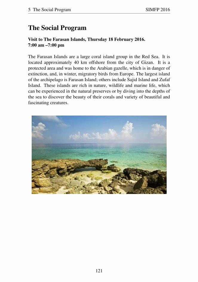
The Social ProgramVisit to The Farasan Islands, Thursday 18 February 2016.7:00 am –7:00 pm

The Farasan Islands are a large coral island group in the Red Sea. It islocated approximately 40 km offshore from the city of Gizan. It is aprotected area and was home to the Arabian gazelle, which is in danger ofextinction, and, in winter, migratory birds from Europe. The largest islandof the archipelago is Farasan Island; others include Sajid Island and ZufafIsland. These islands are rich in nature, wildlife and marine life, whichcan be experienced in the natural preserves or by diving into the depths ofthe sea to discover the beauty of their corals and variety of beautiful andfascinating creatures.

121

SIMFP 2016The Fifth Saudi International Meeting on Frontiers of PhysicsJazan University, Jazan, Saudi Arabia16-18 February 2016

Meeting Book

Organizers:

University Vice-Presidency for Quality and Academic Development,Physics Department and Faculty of Science,@ Jazan University, Saudi Arabia.

http://www.jazanu.edu.sa/SIMFP2016

SIM

FP20

16Th

eFi

fthS

audi

Inte

rnat

iona

lMee

ting

onFr

ontie

rsof

Phy

sics

Department of Physics, Faculty of Science, Jazan University.Gizan 22822 P.O. Box 114, Kingdom of Saudi Arabia.c©2016 SIMFP 2016 Committee, Jazan University, All rights reserved.

SIMFP 2016 6

124


Recommended