34
Red Hot 40 Transceiver - © 1999-2011, Hendricks QRP Kits The Red Hot 40 Construction Manual A High Performance QRP CW Transceiver Kit For 40m Hendricks QRP Kits Revision 2.0 December 2011

Red Hot 40 Transceiver - © 1999-2011, Hendricks QRP Kits
The Red Hot 40 Construction Manual
A High Performance QRP CW Transceiver Kit For 40m
Hendricks QRP Kits Revision 2.0
December 2011
Red Hot 40 Transceiver - © 1999-2011, Hendricks QRP Kits
Contents
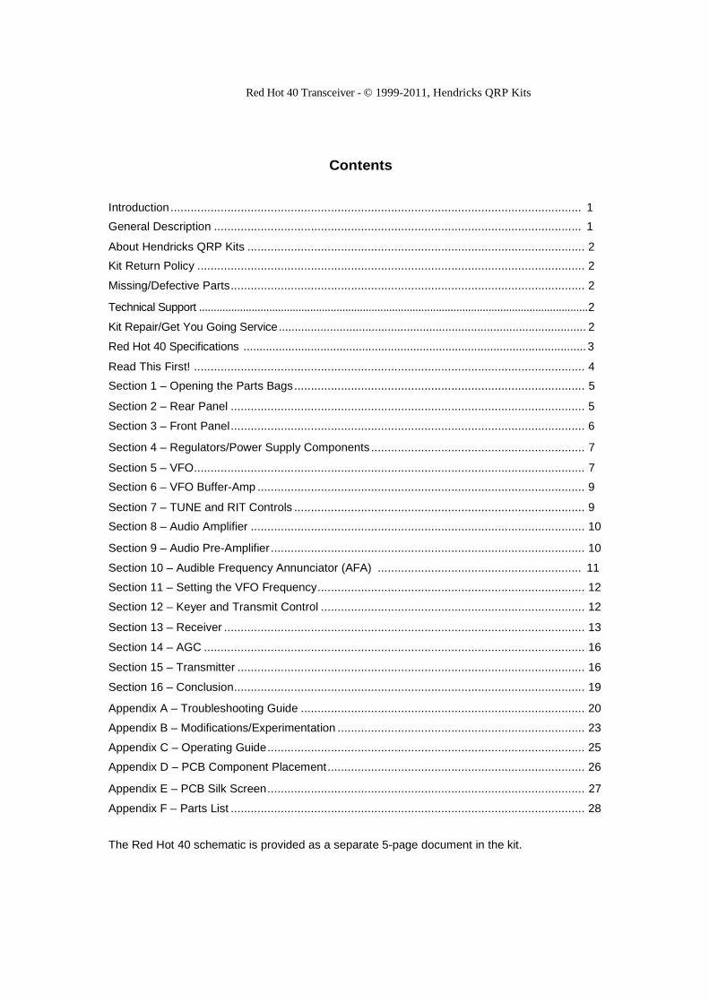
Introduction ........................................................................................................................... 1
General Description .............................................................................................................. 1
About Hendricks QRP Kits ..................................................................................................... 2
Kit Return Policy .................................................................................................................... 2
Missing/Defective Parts .......................................................................................................... 2
Technical Support ..................................................................................................................................... 2
Kit Repair/Get You Going Service ................................................................................................ 2
Red Hot 40 Specifications ........................................................................................................... 3
Read This First! ..................................................................................................................... 4
Section 1 – Opening the Parts Bags ....................................................................................... 5
Section 2 – Rear Panel .......................................................................................................... 5
Section 3 – Front Panel .......................................................................................................... 6
Section 4 – Regulators/Power Supply Components ................................................................ 7
Section 5 – VFO ..................................................................................................................... 7
Section 6 – VFO Buffer-Amp .................................................................................................. 9
Section 7 – TUNE and RIT Controls ....................................................................................... 9
Section 8 – Audio Amplifier .................................................................................................... 10
Section 9 – Audio Pre-Amplifier .............................................................................................. 10
Section 10 – Audible Frequency Annunciator (AFA) ............................................................. 11
Section 11 – Setting the VFO Frequency ................................................................................ 12
Section 12 – Keyer and Transmit Control ............................................................................... 12
Section 13 – Receiver ............................................................................................................ 13
Section 14 – AGC .................................................................................................................. 16
Section 15 – Transmitter ........................................................................................................ 16
Section 16 – Conclusion ......................................................................................................... 19
Appendix A – Troubleshooting Guide ..................................................................................... 20
Appendix B – Modifications/Experimentation .......................................................................... 23
Appendix C – Operating Guide ............................................................................................... 25
Appendix D – PCB Component Placement ............................................................................. 26
Appendix E – PCB Silk Screen ............................................................................................... 27
Appendix F – Parts List .......................................................................................................... 28
The Red Hot 40 schematic is provided as a separate 5-page document in the kit.

Red Hot 40 Transceiver - © 1999-2011, Hendricks QRP Kits Page left blank
Red Hot 40 Transceiver - © 1999-2011, Hendricks QRP Kits
1
The Red Hot 40 - Construction Manual
Introduction
The Red Hot 40 is a high performance QRP CW transceiver kit for the 40m band. It has been designed to operate well in the presence of large out-of-band (short-wave broadcast) and in-band (contest station just down the road) unwanted signals. It should easily meet the requirements of most QRP’ers, from the most competitive contester to the casual operator.
The kit contains all the parts needed to build a complete working radio. The only things the user will have to supply are a power source, loudspeaker or headphones, a set of paddles or straight key (suitably wired) and a matched 40m antenna system.
The kit is designed so that no wiring-up is required - all the components are mounted on a single double-sided with plated through holes, solder masked and silk screened printed circuit board that measures 4.5” by 5”. Pre-drilled front and rear panels with U shaped top and bottom panels are provided that form a clamshell type case that is smart, strong and functional. The case is red anodized aluminum with an engraved legend.
General Description
The Red Hot 40 is a single band QRP CW transceiver optimized for good RF performance rather than for low current drain. As such, it is suited mainly for operation from home-based stations or portable operations with fairly large battery capability (e.g. field day). On receive the current drain can be as much as 150mA. It can produce any output power from 0 to over 5 Watts. The output power is set with a small trim pot inside the rig.
The Red Hot 40 uses fully electronic RX/TX switching (no relays) that gives very smooth, thump-free, semi-break-in operation. The transmit output waveform is edge rate controlled to minimize bandwidth usage. As a bonus, this makes for very nice sounding Morse code on the air.
The Red Hot 40 offers many advanced features that make it easy to use.
The Red Hot 40 has a single conversion superheterodyne receiver and an equivalent single stage down-conversion transmitter. The I.F. is 9MHz with the VFO at 2MHz.
The Red Hot 40 was originally designed to utilize either a 1 turn or a 10 turn TUNE pot. The Red Hot 40 kit is supplied with a 10 turn pot as standard. The Red Hot 40 also has an RIT pot with center detent.
No frequency calibration or scale is needed because the rig has a built in frequency counter, known as the Audible Frequency Annunciator (AFA). This plays the KHz digits of t he f r equenc y t o yo u in Mo rse c ode ov e r t he speaker/headphones. The AFA has two modes of operat ion. Manual mode, where the f requency is announced only when you press the front panel push-button, and automatic mode, where the AFA “pips” at every KHz as you tune up or down the band, then, recognizes when you stop tuning, and announces the frequency automatically.
The Red Hot 40 has a built in Morse code keyer chip from the Embedded Research TiCK line. This keyer allows you to swap the paddles over, set the speed, tune-up, run straight key mode and run in either iambic A or B modes.
The Red Hot 40 is VFO tuned. Much attention has been paid to making the VFO as stable as possible. Some warm- up drift is to be expected, as, from cold, the rig will warm-up significantly due to the large amount of current sacrificed in making the receiver front-end performance satisfactory. Typical warm-up drift is in the region of a few hundred Hz.
The Red Hot 40 receiver has a single AGC loop. The user still has ultimate front-end signal level control - the rig includes an RF Attenuator pot (rear panel mounted).
The receiver consists of a double tuned Cohn bandpass filter feeding a moderate gain tuned FET pre-amplifier (about 6 to 8dB gain, just enough to overcome mixer loss). This feeds a +7dBm level Minicircuits TUF-1 diode-ring double balanced mixer. The mixer output is fed into a broadband 50Ω terminated amplifier that runs enough current to ensure the 2nd and 3rd order intercept points (IP2/3) of the radio are not compromised. The output of this amplifier is terminated with a 50Ω -6dB pad then fed to the four crystal main receive filter. The crystals used for the Red Hot 40 were specially selected and matched to within 50Hz (or better), ensuring a flat topped narrow-band response that is a joy to listen to.
The main filter is followed by a low noise IF amplifier with a matched roofing crystal filter feeding the product detector. The roofing filter removes a lot of opposite sideband noise that would otherwise be present as audio noise in the
Red Hot 40 Transceiver - © 1999-2011, Hendricks QRP Kits hibited
2
product detector’s output. Careful attention has been paid to the IF layout resulting in an overall stopband attenuation that is remarkably good.
The product detector (NE602) feeds balanced audio to a simple low-pass op-amp filter/amplifier with a cutoff frequency around 1.2KHz and a passband gain of about 11dB. The output of this is fed via the TX/RX mute FET to another bandpass filter/amplifier stage that has a center frequency of 650Hz, a Q of 5 and a gain of about 30dB. The output of this is fed to the 1W LM380N audio amplifier via the front panel mounted volume control.
The transmitter mixes the VFO and a carrier oscillator down to 7MHz, filters it and amplifies it to a user adjustable level up to about 7W. The class A driver stage uses a parallel pair of PN2222A transistors that drive the 2SC1969 output power transistor in class C. This transistor uses the rear panel of the rig as its heatsink.
The transmitter output filtering uses a novel harmonic attenuation arrangement that was described in the ARRL QEX journal. This significantly reduces transmitted harmonics. A spectrum analyzer plot shows them all (including 2nd and 3rd harmonics) to be below –70dB from the main carrier.
TX/RX changeover is all electronic. When a paddle key is pressed, the TiCK output drives a switching circuit that provides a linearly ramped transmit power supply rail to the low power transmit stages. This ensures a clean, almost ideally shaped transmit output RF envelope. Likewise, at the end of a Morse code element, the TiCK output drives the switching circuitry to ensure a linearly ramped trailing edge to the transmit power. This ensures a clean tail end for the output RF envelope.
The RX mute signal is also derived from the transmit timing/switching circuitry. The mute signal ensures the AGC is disabled and the receiver is muted prior to the transmit output envelope rise, and that the transmit output envelope is complete, and the receiver stable, prior to enabling the AGC and opening the receiver mute once more. This all happens in the space of a few milliseconds, which gives the rig semi-break-in capabilities. Full break-in operation would be possible with small modifications to the timing components in the TX/RX switching and RX Mute FET timing control circuits – the experimentation for this is left to the user as a quick survey of users showed that semi-break-in is the preferred mode of most CW operators.
Missing/Defective Parts
Missing or defective parts will be replaced free of charge for a period of 30 days from when we ship the kit to you. After this time we will have to charge for spare parts. Please open and inventory the kit as soon as you receive it.
Technical Support
For simple questions please use email to obtain technical support. Send emails to [email protected]. We will endeavor to answer all emails within 48 hours.
Red Hot 40 Transceiver - © 1999-2011, Hendricks QRP Kits
3
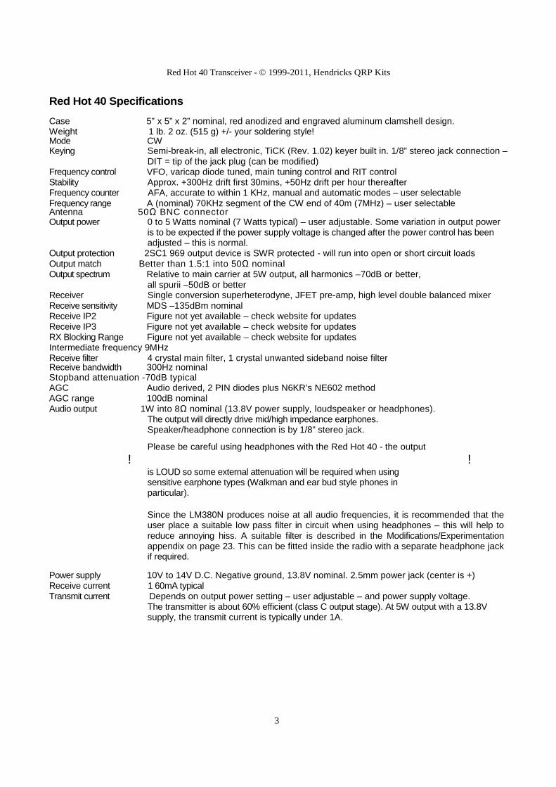
Red Hot 40 Specifications
Case 5” x 5” x 2” nominal, red anodized and engraved aluminum clamshell design. Weight 1 lb. 2 oz. (515 g) +/- your soldering style! Mode CW Keying Semi-break-in, all electronic, TiCK (Rev. 1.02) keyer built in. 1/8” stereo jack connection –
DIT = tip of the jack plug (can be modified) Frequency control VFO, varicap diode tuned, main tuning control and RIT control Stability Approx. +300Hz drift first 30mins, +50Hz drift per hour thereafter Frequency counter AFA, accurate to within 1 KHz, manual and automatic modes – user selectable Frequency range A (nominal) 70KHz segment of the CW end of 40m (7MHz) – user selectable Antenna 50Ω BNC connector Output power 0 to 5 Watts nominal (7 Watts typical) – user adjustable. Some variation in output power
is to be expected if the power supply voltage is changed after the power control has been adjusted – this is normal.
Output protection 2SC1 969 output device is SWR protected - will run into open or short circuit loads Output match Better than 1.5:1 into 50Ω nominal Output spectrum Relative to main carrier at 5W output, all harmonics –70dB or better,
all spurii –50dB or better Receiver Single conversion superheterodyne, JFET pre-amp, high level double balanced mixer Receive sensitivity MDS –135dBm nominal Receive IP2 Figure not yet available – check website for updates Receive IP3 Figure not yet available – check website for updates RX Blocking Range Figure not yet available – check website for updates Intermediate frequency 9MHz Receive filter 4 crystal main filter, 1 crystal unwanted sideband noise filter Receive bandwidth 300Hz nominal Stopband attenuation -70dB typical AGC Audio derived, 2 PIN diodes plus N6KR’s NE602 method AGC range 100dB nominal Audio output 1W into 8Ω nominal (13.8V power supply, loudspeaker or headphones).
The output will directly drive mid/high impedance earphones. Speaker/headphone connection is by 1/8” stereo jack.
Please be careful using headphones with the Red Hot 40 - the output
! ! is LOUD so some external attenuation will be required when using sensitive earphone types (Walkman and ear bud style phones in particular).
Since the LM380N produces noise at all audio frequencies, it is recommended that the user place a suitable low pass filter in circuit when using headphones – this will help to reduce annoying hiss. A suitable filter is described in the Modifications/Experimentation appendix on page 23. This can be fitted inside the radio with a separate headphone jack if required.
Power supply 10V to 14V D.C. Negative ground, 13.8V nominal. 2.5mm power jack (center is +) Receive current 1 60mA typical Transmit current Depends on output power setting – user adjustable – and power supply voltage.
The transmitter is about 60% efficient (class C output stage). At 5W output with a 13.8V supply, the transmit current is typically under 1A.
Red Hot 40 Transceiver - © 1999-2011, Hendricks QRP Kits
4
Read This First!
Construction of the Red Hot 40 is best done in sections, one at a time. The manual therefore uses the “build-a-section, test-a-section” method. Building it this way saves lots of trouble in the long run. The Red Hot 40 is a fairly complex radio so you must make sure you positively identify the parts correctly prior to soldering them into the PCB. Special care should be exercised when identifying the capacitors for the transmit amplifier output filter. This uses 100V components - these should not be mixed up with the lower voltage parts used elsewhere. There are part identification tips and insertion/mounting details throughout the manual.
Also, please pay careful attention to the winding of the toroids. They can only be wound one way properly. Pictures are provided to help you to do this correctly.
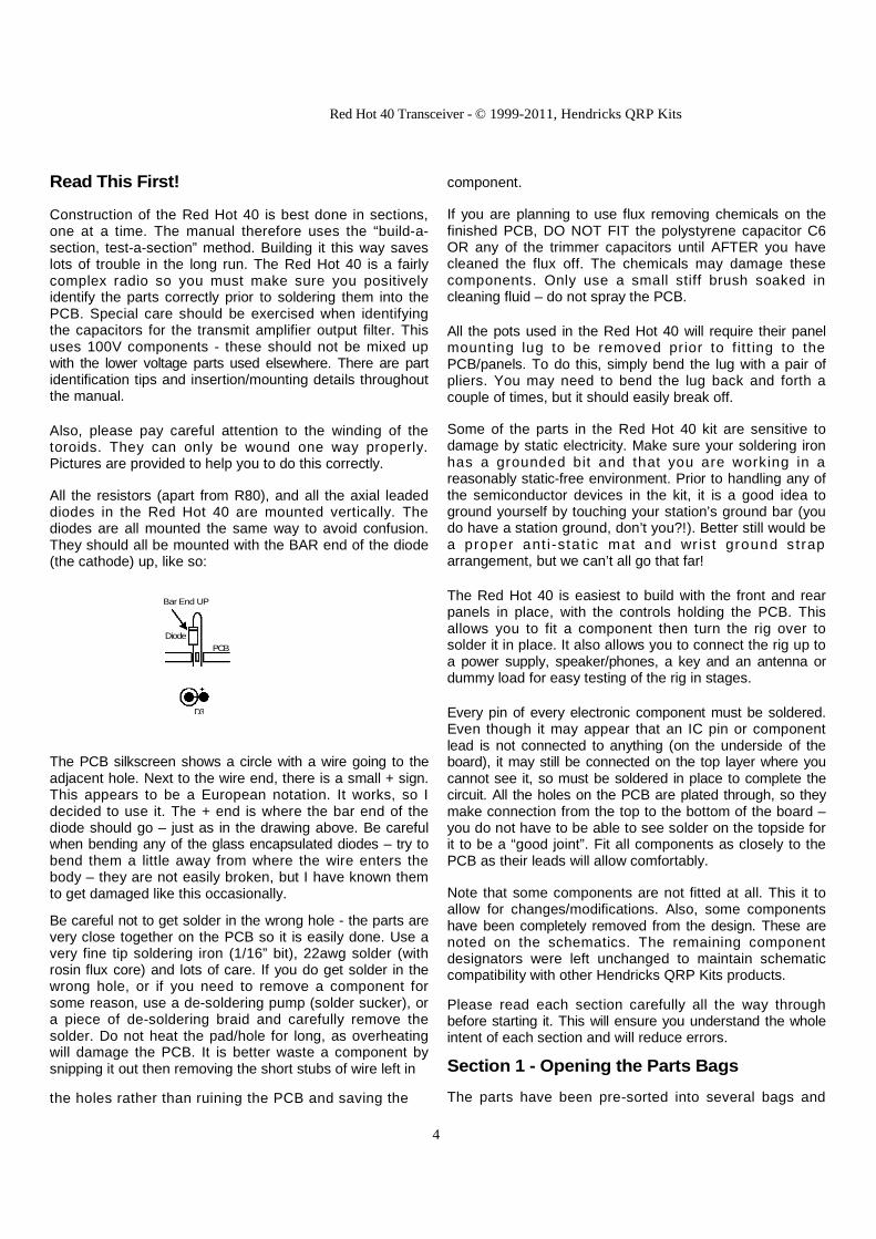
All the resistors (apart from R80), and all the axial leaded diodes in the Red Hot 40 are mounted vertically. The diodes are all mounted the same way to avoid confusion. They should all be mounted with the BAR end of the diode (the cathode) up, like so:
Bar End UP
The PCB silkscreen shows a circle with a wire going to the adjacent hole. Next to the wire end, there is a small + sign. This appears to be a European notation. It works, so I decided to use it. The + end is where the bar end of the diode should go – just as in the drawing above. Be careful when bending any of the glass encapsulated diodes – try to bend them a little away from where the wire enters the body – they are not easily broken, but I have known them to get damaged like this occasionally.
Be careful not to get solder in the wrong hole - the parts are very close together on the PCB so it is easily done. Use a very fine tip soldering iron (1/16” bit), 22awg solder (with rosin flux core) and lots of care. If you do get solder in the wrong hole, or if you need to remove a component for some reason, use a de-soldering pump (solder sucker), or a piece of de-soldering braid and carefully remove the solder. Do not heat the pad/hole for long, as overheating will damage the PCB. It is better waste a component by snipping it out then removing the short stubs of wire left in
the holes rather than ruining the PCB and saving the
component.
If you are planning to use flux removing chemicals on the finished PCB, DO NOT FIT the polystyrene capacitor C6 OR any of the trimmer capacitors until AFTER you have cleaned the flux off. The chemicals may damage these components. Only use a small stiff brush soaked in cleaning fluid – do not spray the PCB.
All the pots used in the Red Hot 40 will require their panel mounting lug to be removed prior to f itt ing to the PCB/panels. To do this, simply bend the lug with a pair of pliers. You may need to bend the lug back and forth a couple of times, but it should easily break off.
Some of the parts in the Red Hot 40 kit are sensitive to damage by static electricity. Make sure your soldering iron has a grounded bit and that you are working in a reasonably static-free environment. Prior to handling any of the semiconductor devices in the kit, it is a good idea to ground yourself by touching your station’s ground bar (you do have a station ground, don’t you?!). Better still would be a proper ant i -stat ic mat and wr is t ground s t rap arrangement, but we can’t all go that far!
The Red Hot 40 is easiest to build with the front and rear panels in place, with the controls holding the PCB. This allows you to fit a component then turn the rig over to solder it in place. It also allows you to connect the rig up to a power supply, speaker/phones, a key and an antenna or dummy load for easy testing of the rig in stages.
Every pin of every electronic component must be soldered. Even though it may appear that an IC pin or component lead is not connected to anything (on the underside of the board), it may still be connected on the top layer where you cannot see it, so must be soldered in place to complete the circuit. All the holes on the PCB are plated through, so they make connection from the top to the bottom of the board – you do not have to be able to see solder on the topside for it to be a “good joint”. Fit all components as closely to the PCB as their leads will allow comfortably.
Note that some components are not fitted at all. This it to allow for changes/modifications. Also, some components have been completely removed from the design. These are noted on the schematics. The remaining component designators were left unchanged to maintain schematic compatibility with other Hendricks QRP Kits products.
Please read each section carefully all the way through before starting it. This will ensure you understand the whole intent of each section and will reduce errors.
Section 1 - Opening the Parts Bags
The parts have been pre-sorted into several bags and
Diode PCB
D3
Red Hot 40 Transceiver - © 1999-2011, Hendricks QRP Kits
5
sealed. The bags are doubly protected: they are inside an outer bag that is also sealed. This should ensure no parts go astray in shipping. Check that you have the following items in your kit:
1. Manual – you’re reading it right now 2. The top/bottom/front/rear case pieces 3. 6’ x 18awg pre-assembled power cord 4. Large sealed plastic bag containing:
a) Double sided, plated through hole, solder masked, silk screened printed circuit board
b) Plastic bag containing resistors and trimpots (to make identification easier, the 1% resistors are contained in another small plastic bag inside this one)
c) Plastic bag containing capacitors and trimcaps (the 0.1µF, 0.01µF and 820pF capacitors are separated in their own small bags within this bag)
d) Plastic bag containing discrete semiconductors e) Plastic bag containing 9MHz crystals, and a small
plastic bag with the tiny 100KHz crystal f) Plastic bag with the IC’s on a piece of anti-static
foam g) Plastic bag containing three small reels of wire,
toroids and inductors h) Plastic bag containing hardware i) Plastic bag containing controls and connectors
In the discrete semiconductors bag you will find 17 small 1N914 diodes strung together (“tape and reel” fashion). You will also find two similar looking diodes in their own small plastic bag - these are the 1 N754A 6.8V zener diodes (item 75). Do not mix these diodes up with the 1N914 diodes.
Sort the transistors carefully. All the TO-92 cased devices look the same. The lettering/numbering on them is very small – if necessary, use a magnifying glass to identify the parts. Notice that 3 of the TO-92 devices have only 2 leads. These are diodes. Two of them are PIN diodes for the AGC and the fourth is the varicap for the VFO. Also, note that the two voltage regulators are in this bag.
Using the parts list at the back of this manual, select and identify the other parts. In particular, pay careful attention to the capacitors. There are several instances where there are capacitors of the same value, but where the type of capacitor and the job it is intended to do are quite different. An identification guide is provided alongside the parts list. The capacitors used in the transmitter output stage are most critical. These must be 100V low dielectric loss types as there are very high RF voltages at this point in the circuit. Make sure you get this right - you don’t want to let
any smoke out of your rig! Also, the 270pF C0G capacitor for the VFO is critical. This capacitor has the marking “C0G” on it just below the value “271”.
The tiny 100KHz crystal (X8) should be handled with great care – it is very small and fragile and easily get lost or broken. Use hot glue or wax to hold it in place when fitted.
Check that you have all the parts listed in the parts list. If you have any missing or obviously broken parts, or if you are not sure of any part’s identification please contact Hendricks QRP Kits for a replacement/advice straight away. Send email to [email protected]
Section 2 - Rear Panel
The rear panel should be assembled prior to the front panel to allow easier alignment of the panels with the PCB.
Fit and solder the two stereo jack sockets J1 and J3 to the PCB. Make sure their fixing nuts are removed and they are pushed down flat against the board before soldering them.
Loose fit the BNC, J2, the power connector J4 and the RF attenuation pot, VR3 to the PCB. Place the flat washer on the pot VR3 but leave the toothed washer off the BNC.
Align the PCB with the rear panel. Place the toothed washer and ring nut on the BNC finger tight.
Place the two nuts on the stereo jack sockets J1 and J3 finger tight. Place the nut on the shaft of the pot (VR3) finger tight.
Making sure the PCB is perpendicular to, and level across the width of, the rear panel, turn it over and solder the BNC (J2) and the pot, VR3, in place.
Next, look at the alignment of the power connector, J4, through the hole in the rear panel. Make sure it is centered in the hole before soldering it in place. Fill the power connector’s PCB through holes with solder – quite a bit of current is going to be flowing here.
The transmitter output power transistor will be fitted later – do not solder it in at this time.
Carefully file away the anodizing around the rear panel GND connection point. This will ensure a good ground from the PCB to the panel.
Find the solder lug (item 109) and cut the end off it so that when positioned on the rear panel it does not protrude into R80’s PCB space. Fit it to the rear panel grounding hole at the opposite end of the rear panel to the jack sockets. Use 4-40 1/4” screw (item 110) and nut (item 111) to hold the solder lug in place. Orient it so that it aligns with
Red Hot 40 Transceiver - © 1999-2011, Hendricks QRP Kits
6
the GND pad on the PCB. Once aligned and tightened in place, bend and solder the lug directly to the GND pad on the PCB with a healthy dab of solder. This connection needs to be as electrically short as it can possibly be.
Section 3 - Front Panel
You will have to twist and/or bend the lugs of the 10 turn pot a little to make it fit. Alternatively, you can file or cut a tiny bit off the lugs to make them appear vertical to the PCB and fit it without any bending. Do not solder the TUNE pot in place just yet – just make sure it is going to fit the holes nicely.
Cut off about 3/16th inch of the 10 turn pot’s to get the large tuning knob to fit nicely back against the front panel. Do this in a vise, prior to fitting and soldering the pot - it’s much easier than trying to cut it when it’s mounted!
Note that SW1 and SW2 are fitted underneath the PCB, on the track side. Fit and solder them into the PCB at this time. Make sure they are flat against the PCB or they will not line up with the front panel holes.
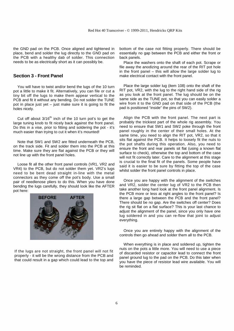
Loose fit all the other front panel controls (VR1, VR2 and VR4) to the PCB, but do not solder them yet. VR2’s lugs need to be bent dead straight in-line with the metal connectors as they come off the pot’s body. Use a small pair of needlenose pliers to do this. When you have done bending the lugs carefully, they should look like the AFTER pot here:
If the lugs are not straight, the front panel will not fit properly - it will be the wrong distance from the PCB and that could result in a gap which could lead to the top and
bottom of the case not fitting properly. There should be essentially no gap between the PCB and either the front or back panels.
Place the washers onto the shaft of each pot. Scrape or file away the anodizing around the rear of the RIT pot hole in the front panel – this will allow the large solder lug to make electrical contact with the front panel.
Place the large solder lug (item 108) onto the shaft of the RIT pot, VR2, with the lug to the right hand side of the rig as you look at the front panel. The lug should be on the same side as the TUNE pot, so that you can easily solder a wire from it to the GND pad on that side of the PCB (the pad is positioned “inside” the pins of SW2).
Align the PCB with the front panel. The next part is probably the trickiest part of the whole rig assembly. You need to ensure that SW1 and SW2 poke through the front panel roughly in the center of their small holes. At the same time, you need to align the RIT pot, VR2, so that it sits flat against the PCB. It helps to loosely fit the nuts to the pot shafts during this operation. Also, you need to ensure the front and rear panels sit flat (using a known flat surface to check), otherwise the top and bottom of the case will not fit correctly later. Care to the alignment at this stage is crucial to the final fit of the panels. Some people have said it is easier to be sure by fitting the top of the case whilst solder the front panel controls in place.
Once you are happy with the alignment of the switches and VR2, solder the center lug of VR2 to the PCB then take another long hard look at the front panel alignment. Is the PCB more or less at right angles to the front panel? Is there a large gap between the PCB and the front panel? There should be no gap. Are the switches off center? Does the rig sit flat on a flat surface? This is your last chance to adjust the alignment of the panel, since you only have one lug soldered in and you can re-flow that joint to adjust everything.
Once you are entirely happy with the alignment of the controls then go ahead and solder them all to the PCB.
When everything is in place and soldered up, tighten the nuts on the pots a little more. You will need to use a piece of discarded resistor or capacitor lead to connect the front panel ground lug to the pad on the PCB. Do this later when you have the piece of resistor lead wire available. You will be reminded.

Red Hot 40 Transceiver - © 1999-2011, Hendricks QRP Kits
7
Section 4 - Regulators/Power Supply Components
Insert and solder the following components:
Item 84 U2 L78L08ACZ Item 85 U8 LM78L05ACZ Item 74 D1 1N5822
Item 67 C9 0.1jtF Item 67 C10 0.1jtF Item 70 C11 10jtF Item 67 C12 0.1jtF Item 67 C91 0.1jtF Item 70 C92 10jtF Item 67 C93 0.1jtF Item 71 C95 100jtF
These components are on sheets 1 and 5 of the circuit diagram.
Connect a suitable (13.8V nominal) power supply to the power input jack J4 whilst measuring the input current on a meter (set to 50mA full scale deflection, FSD, or thereabouts). Turn on the power. The input current should be no more than 10mA. If it is just a little more than this, up to, say double, then you may have a problem with the actual voltage regulators U2 or U8 and further detailed investigation will be necessary. If all is well (typically you will see about 8mA), then turn off, connect the power up directly without the meter and turn on again. With the meter set to read DC Volts (20V range or thereabouts), measure the voltages at the following points (red lead or +) with respect to GND (black lead or -)
J4 center pin (at the rear of J4) - should be the same as the supply voltage (+13.8V)
D1 cathode (bar end - the wire facing the front of the rig) - should be about 0.3V less than the power supply rail (+1 3.5V)
U9 pin 1 (square pad) - should be between +4.75 and +5.25V (+5V +/- 0.25V)
Q2 drain (Q2 pin nearest U2) - should be between +7.6 and +8.4V (+8V +/- 0.4V)
If you don’t see these voltages there is a problem. Look for short circuits between tracks, particularly between the pins of U2 and U8. Sometimes tiny silvers of metal can be made when this type of component is inserted into a PCB, this can short pins together on the topside of the PCB, so make sure to look there too. If there is no solder bridging
and everything is soldered correctly, then suspect a defect in the voltage regulator/s.
Section 5 - VFO
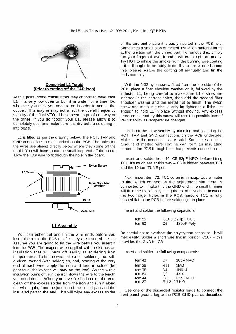
The first component to fit is the VFO main tuned circuit inductor, L1. Locate the T50-7 toroid core (item 98, white, bigger than the others), the 28awg wire (the thinest enameled wire, red, item 131), the two black fiber shoulder washers (Item 112), the 6-32 x 5/8” nylon screw (item 113) and the 6-32 nut for it (item 107). Cut 40” of the wire.
Hold the T50-7 core in your left hand at the bottom of the toroid, with the white face up. With your right hand, thread about 2” of one end of the wire through the core from the top of the toroid. Wrap the long end of the wire around the toroid and thread it up through the toroid from the bottom to complete the second turn clockwise from where you laid the first turn (the first turn was when you pushed the wire through at the start). Holding the short end of the wire tight against the toroid body with your left hand, pull the long end of the wire tight with your right hand so the winding is kept tight and each turn is placed beside the previous (left to right). Each pass through the center of the toroid is 1 turn.
Continue adding turns like this up to turn number 12. At the “end” of turn number 12, you need to bend the long end of the wire back double on itself to make a 2” tap. With the wire bent back on itself, grab the small loop that is formed and twist the tap many times around so that it forms what looks like a single wire. Make sure you twist it real tight so that the twists go all the way back to the body of the toroid. Then, take the long end of the wire again. Pass it up through the bottom of the toroid to form turn number 13.
Continue adding turns till you have 54 of them on the toroid all nice and tightly wound. Loose windings will allow changes in the inductance to occur which will affect the frequency stability of your VFO. 54 turns fit just snug on this toroid. Make sure they are evenly spaced. Here is how your L1 should look at this point:
Red Hot 40 Transceiver - © 1999-2011, Hendricks QRP Kits
8
Completed L1 Toroid
(Prior to cutting off the TAP loop)
At this point, some constructors may choose to bake their L1 in a very low oven or boil it in water for a time. Do whatever you think you need to do in order to anneal the copper. This may or may not affect the overall frequency stability of the final VFO - I have seen no proof one way or the other. If you do “cook” your L1, please allow it to completely cool and make sure it is dry before soldering it into place.
L1 is fitted as per the drawing below. The HOT, TAP and GND connections are all marked on the PCB. The holes for the wires are almost directly below where they come off the toroid. You will have to cut the small loop end off the tap to allow the TAP wire to fit through the hole in the board.
PCB
L1 Assembly
You can either cut and tin the wire ends before you insert them into the PCB or after they are inserted. Let us assume you are going to tin the wire before you insert it into the PCB. The magnet wire supplied with the kit has an insulation that will burn off easily at soldering iron temperatures. To tin the wire, take a hot soldering iron with a clean, wetted (with solder) tip, and, starting at the very end of each wire, apply the iron and feed in solder (be generous, the excess will stay on the iron). As the wire’s insulation burns off, run the iron down the wire to the length you need tinned. When you have finished tinning the end, clean off the excess solder from the iron and run it along the wire again, from the junction of the tinned part and the insulated part to the end. This will wipe any excess solder
off the wire and ensure it is easily inserted in the PCB hole. Sometimes a small blob of melted insulation material forms at the junction with the tinned part. To remove this, simply run your fingernail over it and it will crack right off neatly. Try NOT to inhale the smoke from the burning wire coating – it is thought to be fairly toxic. If you are worried about this, please scrape the coating off manually and tin the ends normally.
With the 6-32 nylon screw fitted from the top side of the PCB, place a fiber shoulder washer on it, followed by the inductor L1, being careful to make sure L1’s wires are inserted in the correct holes, then add the second fiber shoulder washer and the metal nut to finish. The nylon screw and metal nut should only be tightened a little: just enough to hold L1 in place without moving. Any excess pressure exerted by this screw will result in possible loss of VFO stability as temperature changes.
Finish off the L1 assembly by trimming and soldering the HOT, TAP and GND connections on the PCB underside. Make sure the connections are solid. Sometimes a small amount of melted wire coating can form an insulating barrier in the PCB through hole that prevents connection.
Insert and solder item 46, C5 82pF NPO, before fitting TC1. It’s much easier this way – C5 is hidden between TC1 and the 10 turn TUNE pot.
Next, insert item 72, TC1 ceramic trimcap. Use a meter to find which connection the adjustment slot metal is connected to – make this the GND end. The small trimmer will fit in the PCB nicely using the extra GND hole between the two larger holes in the PCB. Ensure TC1 is fully pushed flat to the PCB before soldering it in place.
Insert and solder the following capacitors:
Item 55 C108 270pF C0G Item 60 C6 180pF Poly
Be careful not to overheat the polystyrene capacitor - it will melt easily. Solder a short wire link in position C107 – this provides the GND for C6.
Insert and solder the following components:
Item 42 C7 10pF NPO Item 36 R11 1MΩ Item 75 D4 1N914 Item 80 Q2 J310 Item 44 C8 27pF NPO Item 27 R 1 2 2 7 KΩ
Use one of the discarded resistor leads to connect the front panel ground lug to the PCB GND pad as described
Metal Nut
Nylon Screw
L1 Toroid
Fiber Shoulder Washer
Red Hot 40 Transceiver - © 1999-2011, Hendricks QRP Kits
9
earlier.
Insert and solder the following components:
Item 41 C86 4.7pF NPO Item 23 R81 10KΩ Item 75 D23 1N914
Item 67 C87 0.1µF
These components form the built-in RF probe that you are going to use to test some of the circuits.
Find a 5” piece of scrap hook-up wire to use as a jumper. Connect it from the junction of C8 and R12 to the anode of D23 (that’s the junction of D23, R81 and C86). If you don’t have any hook-up wire, use a 5” piece of the green 26-awg magnet wire provided with the kit, but don’t throw it away afterwards, you’ll need it again. Connect power to the rig and turn it on.
Using your meter set to a low voltage range (DC, 2V range is good), measure the voltage between GND (black probe or -) and the “RF” test point on the PCB (red probe or +). You should get between +0.5V and +1.5V. This means the VFO is producing RF nicely. Don’t worry about the frequency of the VFO for the moment.
If you don’t get any voltage here you have something wrong in the VFO circuitry. Go back over and check your work. Look for solder bridges (check for solder splashes that could be shorting out TC1), components in the wrong way and pay particular attention to L1’s PCB connections. When you are done, disconnect the 5” hookup wire from the VFO end, but leave it connected to the RF probe circuit.
If you have access to an oscilloscope, you can probe the same point as the hook-up wire is connected to. You should see a nice clean 1 to 1 .5V peak-to-peak sinewave at about 2MHz.
Section 6 - VFO Buffer-Amp
Insert and solder the following components:
Item 86 Q3 2N5179 Item 81 Q4 PN2222A Item 21 R13 5.6KΩ Item 29 R14 47KΩ Item 11 R15 470Ω
Item 16 R16 1.5KΩ (not 7.5KΩ!) Item 3 R17 10Ω Item 6 R 1 8 4 7Ω Item 67 C13 0.1µF Item 44 C14 27pF NPO
Item 67 C15 0.1µF Item 51 C66 330pF Item 67 C67 0.1µF
Connect the loose end of the 5” piece of hook-up wire to the junction of C15 and U3 (the other end should still be connected to the RF probe circuit). Connect power to the rig and turn it on.
Using your meter set to a low voltage range (DC, 2V range is good), measure the voltage between GND (black or -) and the RF test point on the PCB (red or +). You should get somewhere between +1V and +2V. This means the buffer/amp is doing its job properly.
Section 7 - TUNE and RIT controls
Insert and solder the following components:
Item 79 Q1 2N5457 Item 75 D2 1N914 Item 90 U1 LF351N Item 38 R1 8.2KΩ 1% Item 32 R2 100KΩ Item 39 R3 10KΩ 1% Item 39 R4 10KΩ 1% Item 35 R5 820KΩ Item 40 R6 33KΩ 1% Item 40 R7 33KΩ 1% Item 36 R8 1 MΩ Item 33 R9 220KΩ Item 135 R10 82µH RFC – see text Item 37 R100 3.3KΩ 1% Item 67 C1 0.1µF Item 70 C2 10µF Item 67 C4 0.1µF Item 77 D3 MV209
Note that resistors R1, R3, R4, R6, R7 and R100 are 1% tolerance parts (blue bodies). Also note that R10 has been replaced with an 82µH RFC, item 135 – insert the RFC into position R10 on the PCB (vertically).
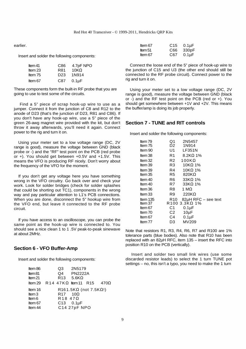
Insert and solder two small link wires (use some discarded resistor leads) to select the 1 turn TUNE pot settings – no, this isn’t a typo, you need to make the 1 turn
Red Hot 40 Transceiver - © 1999-2011, Hendricks QRP Kits
10
links so that the rig tunes the band the right way round – from low to high as you turn the TUNE knob clockwise. To the left of the TUNE pot, as you are looking at the front of the radio, are the two sets of links labeled 1t and 10t. Make the 1t links as shown below (view from front of rig):
10t TUNE Pot Links
Connect power to the rig and turn it on.
Using your meter set to the 20V DC range (or thereabouts), with the black lead (-) to GND, probe the voltage at U1 pin 6 (the junction of U1 pin 6 and R10). Vary the TUNE control from fully counter-clockwise to fully clockwise and note the measured voltage at each extreme.
The voltage should vary from about +10V to about +2V as you turn VR1 clockwise. A little variation in these voltages is not a problem here.
Depending on the accuracy of your meter, try varying the RIT pot and see if the voltage at U1 pin 6 varies at all. We will be testing the RIT pot more fully later, so don’t worry if you can’t do this test now. The voltage should vary by about +/- 0.2V from one end of VR2 to the other at this time.
Section 8 - Audio Amplifier
Insert and solder the following components:
Item 95 U6 LM380N Item 67 C56 0.1µF Item 66 C57 0.01 µF Item 67 C58 0.1µF Item 71 C59 100µF Item 69 C60 4.7µF Item 67 C61 0.1µF Item 71 C62 100µF
Item 3 R57 10Ω Item 1 R58 2.7Ω
Connect a suitable loudspeaker or set of headphones to J1 then connect power and turn the rig on. Make sure that the loudspeaker or phones you use have a STEREO plug fitted (not MONO). You may hear a small click from the speaker/phones upon turn-on. Rotate the volume control VR4 fully clockwise. Using a small piece of wire or a small screwdriver blade, touch the ungrounded end connection of VR4 (the right most terminal as you look at the radio front).
You should hear crackling and/or buzzing from the speaker/phones.
Section 9 - Audio Pre-Amplifier
Insert and solder the following components:
Item 91 U5 LF353N Item 79 Q9 2N5457 Item 63 C43 0.047µF Item 67 C44 0.1µF Item 67 C45 0.1µF Item 62 C46 1500pF Item 62 C47 1500pF Item 70 C48 10µF Item 67 C49 0.1µF Item 70 C50 10µF Item 67 C51 0.1µF Item 65 C52 0.22µF Item 66 C53 0.01 µF Item 66 C54 0.01µF Item 69 C55 4.7µF Item 26 R 4 4 2 2KΩ Item 26 R 4 5 2 2KΩ Item 31 R 4 6 8 2KΩ Item 31 R 4 7 8 2KΩ Item 3 R48 10Ω Item 23 R49 10KΩ Item 23 R50 10KΩ Item 36 R51 1MΩ Item 19 R53 3.9KΩ Item 22 R54 7.5KΩ Item 34 R55 270KΩ Item 28 R 5 6 3 3KΩ Item 75 D13 1N914 Item 75 D14 1N914
Item 75 D15 1N914
Please pay special attention to getting the resistor
values right – many “low RX audio” problems have been
traced to R55 having a 22052 resistor fitted by mistake!
Red Hot 40 Transceiver - © 1999-2011, Hendricks QRP Kits
11
Note that R52 is included for test, setup and modification
purposes and is not soldered in at this time.
Connect the loudspeaker/phones and power-up the
radio again. With the volume control fully clockwise, dab
your test wire/screwdriver tip onto the pads for U4 pins 4
and 5 in turn.
You should hear c rack l ing/buzzing f rom the
speaker/phones again when you dab each pad, but this
time it should sound “bandwidth limited” since it’s going
through a fairly sharp 650Hz bandpass filter. Compare it to
the sound you get by dabbing on the volume control pot
directly and you should easily be able to hear the
difference.
The maximum volume the radio can generate is set with
R56 (33K52). The standard level (as shipped) is set so that for most small speakers and stereo headphones there is not much chance of eardrum busting audio from the rig!
Thus it is set lower than some constructors may like. You
can change R56 to adjust the maximum volume if you like.
Section 10 - Audible Frequency Annunciator
(AFA)
Insert and solder the following components:
Item 94 U10 AFA-40 Using:
Item 133 8pin DIL socket
Item 86 Q22 2N5179
Item 82 Q23 2N3904
Item 75 D27 1N914
Item 50 C97 270pF
Item 67 C98 0.1uF
Item 66 C99 0.01uF
Item 45 C100 33pF
Item 66 C101 0.01uF
Item 67 C102 0.1uF
Item 70 C103 10uF
Item 61 C104 1000pF
Item 45 C106 33pF
Item 18 R86 3.3K52
Item 24 R87 12K52
Item 28 R 8 8 3 3 K 5 2
Item 11 R89 47052
Item 17 R90 2.2K52
Item 14 R911K52 Item 23 R92 10K52
Item 26 R 9 3 2 2 K 5 2
Item 23 R94 10K52
Item 23 R95 10K52
Item 7 R96 10052
Item 32 R102 100K52
Item 120 VR8 10K52 trim pot
Item 97 X8 100KHz crystal
Use the supplied 8pin DIL socket (item 133) to fit U10. This
will allow you to do easy upgrades to the AFA chip in the
future.
Be especially careful when soldering X8 into the board as it
is extremely tiny and fragile. It is a good idea to hold it in
place with a dab of hot glue or wax after you have soldered
it to the board. Note that R92 is near the front of the PCB,
next to the AFA mode setting links LK1-4.
You now have to make some decisions. Do you want the
AFA to operate in Auto mode or Manual mode? Also, do
you want to have a switch to change modes on the fly or a
set of 0.1” headers with jumpers to allow occasional
changes to be effected, or hardwire the AFA mode?
Four links are provided on the PCB to facilitate any of
the above choices, LK1-4. They are positioned so that a
small DPDT slide switch will fit the holes. These can be
fitted on either side of the PCB. If you fit it to the topside,
you will only have access to it when you remove the lid of
the radio (4 screws). If you fit it to the underside of the PCB
you will be able to change modes quite easily from the
underside of the rig if you cut a small rectangular hole in
the bottom of the case to allow access to the slide switch.
If you choose to panel mount a DPDT switch, either on
the front or rear panels, you can use just about any DPDT
switch you have to hand and wire it pin-for-pin back to the
6 holes on the PCB.
I f you only want to change the AFA mode very
occasionally, or if you just want to try each mode for a
while to see what your preference is, then you may
consider putting two small 3-pin 0.1” spacing “headers” into
the LK1-4 holes. You can then use two 0.1” jumper blocks
(just like they use on computer boards to configure the
IRQ/Address etc.) to set the mode (these parts are not
supplied with the kit however).
Alternatively, if you know which mode you want already,
just go ahead and solder small wire links into the PCB. Use
two links. For Auto mode, solder the links into LK1 and
LK3, for manual mode, solder the links into LK2 and LK4.
You can use two discarded resistor leads for the links.
Set the volume control to about half way, the tune control to minimum and the trimpot VR8 to about 1/3 clockwise from fully counter-clockwise. Connect the loudspeaker/phones and power-up the radio. Press the AFA announce push-button SW2. You should hear an
Red Hot 40 Transceiver - © 1999-2011, Hendricks QRP Kits
12
announcement in the speaker/phones in Morse code at about 1800Hz. The frequency of the VFO should be 2.000MHz at this point in which case, the AFA should send “00” in Morse code. However, the announcement may be one of four other things:
a) Nothing at all – something is wrong with the AFA, the 100KHz crystal, or the VFO frequency (too far off frequency and it won’t work) b) ‘0’ in which case there is something wrong with the
VFO signal getting to the AFA c) ‘xxx’, a three digit number (e.g. 965) in which case
the VFO needs adjustment upwards in frequency d) ‘xx’, a two digit number (e.g. 14) in which case the
VFO still needs adjustment downwards in frequency
The next section deals with the tuning of the VFO.
Section 11 - Setting the VFO Frequency
If the AFA announcement is a three-digit number like ‘965’ this means the VFO is too high in frequency. The VFO may be below or above the AFA’s input range for normal operation too – try tweaking TC1 and/or spreading/compressing L1 ’s turns until you get the AFA to respond. You need to adjust the VFO’s trimmer capacitor TC1 so that the lowest RX frequency (with the TUNE pot fully counter-clockwise) is what you want it to be. In most cases you will want the lowest RX frequency to be 7.000MHz. It’s a good idea to set the lowest frequency to ‘999’ so you can guarantee full coverage of the low end of the band.
If you are in AFA Auto mode the AFA will announce frequencies as you tune TC1, after a short pause each time you stop. Notice that you will also hear ‘pips’ as you tune through each KHz. In manual mode, you will need to press the AFA’s announce push-button SW2 every time you want to know the frequency.
Set VR8 to the level you find comfortable to listen too. This will depend on your personal preference and what mode you have the AFA set to. It is adjustable from nothing up to very loud, catering to all tastes.
Section 12 - Keyer and Transmit Control
Insert and solder the following components:
Item 92 U9 TiCK Using: Item 133 8pin DIL Socket Item 82 Q19 2N3904 Item 83 Q20 2N3906 Item 82 Q21 2N3904 Item 70 C65 10jtF Item 66 C88 0.01 jtF Item 66 C89 0.01 jtF Item 67 C90 0.1jtF Item 67 C94 0.1jtF Item 61 C96 1000pF Item 30 R 8 2 5 6K C Item 23 R83 10KC Item 18 R84 3.3KC Item 12 R 8 5 56 0C Item 23 R 9 7 1 0K C Item 17 R98 2.2KC Item 17 R99 2.2KC
Item 120 VR7 10KC trimpot Item 75 D25 1N914 Item 75 D26 1N914
Use the supplied 8-pin DIL socket for U9 – this will make upgrading to the Embedded Research TiCK 4 keyer (with memory) a lot easier. Make sure you insert U9 the correct way round. The label makes it difficult to see the “indent” in the package that identifies the end with pin 1. Diode D24 has been removed from the design.
Set the volume control at half way and the keyer sidetone level control VR7 to about 1/3 clockwise from fully counter-clockwise. Connect up the loudspeaker/phones and power-up the radio again. This time when you turn-on the power you should hear a ‘dit-dit’ in the speaker/phones at the sidetone frequency of about 650Hz. This tells you that the TiCK keyer powered up correctly. The ‘dit-dit’ that you hear is the version of TiCK. If you were to plug in a Super TiCK III instead, you’d hear ‘dit-dit-dit dah’ for “s t”. Likewise, a TiCK 4 sends ‘dit-dit-dit-dit-dah’ at power up.
Power off the rig, connect a set of paddles to J3 and then turn the power back on. Operate your paddles to check both the dit and dah works. Don’t worry if they are the wrong way round at the moment, we’ll get to that later. Press the TiCK programming push-button SW1 and hold it.
You should hear the programming menu sequence of the TiCK keyer ‘s t p a sk m k’ in the speaker/phones. This will repeat if you hold SW1 continuously. The TiCK keyer programming instructions are included in an appendix at
the end of the manual. Let go of SW1 when the TiCK
Red Hot 40 Transceiver - © 1999-2011, Hendricks QRP Kits
13
announces “s”. This allows you to adjust the keyer speed up or down (using the paddles). Hit SW1 again to get out of the setup menu.
Connect your meter (set to 20V DC range or thereabouts) from GND (black or - lead) to the +12VTX signal at the junction of R98 and C94 (red or + lead). You can get at this signal easiest on the looped end of the wire on R98 on the topside of the PCB. At the moment, the meter should read 0V.
Press the TiCK programming button and hold it until you hear ‘s t’ then let go. This puts the rig into tune-up mode (continuous transmit). You should hear a continuous sidetone at this time. The meter should now read about +13.3V. This tests the transmit switching. Hit either the dit or dah paddle or SW1 again to stop the tune-up mode. If you have access to a ‘scope, you can try looking at the +12VTX signal as you send with the paddles. Notice the linear rise and fall waveform that contributes to clean, minimum bandwidth use on the band.
Next you have a decision to make. Are the paddles the right way around for you? You probably already have paddles that are wired up to your liking. The “standard” wiring method is with DIT to the tip of the stereo plug, but there is no “standard” that says which paddle dit has to be! For this reason, there is a way for you to electrically swap the paddles over so that when you first turn the rig on, they will be right for you.
Of course, you can re-program the TiCK to swap the paddles over any time you like, but this information is lost at power off time (unless you upgrade to a TiCK 4 that is!). This feature is nice for guest operators who have different dit/dah preferences to you.
On the PCB, right behind the paddle jack J3 you will see two sets of 4 holes in a row. There are two links labeled ‘DIT’ and ‘DAH’, plus two pairs of holes labeled ‘Cap’. The capacitor holes are there just in case you need to keep RF out of your rig - they decouple the dit and dah lines to GND - they will not normally be required at QRP power levels. 1000pF or 0.01 µF capacitors (not supplied) can be used here but only fit them if they are really needed. The DIT and DAH links have thin PCB traces on the underside of the board. If the paddles are the wrong way round (for you) at power-up, cut the thin traces carefully and, using two insulated jumper wires soldered into the PCB holes, swap the paddles over by crossing the links.
Section 13 - Receiver
First you are going to fit the 9MHz crystals X1-6 (Item 96). Before you insert each crystal, tin its metal case near the bottom of one end with your soldering iron. Do this as quickly as possible - you should be able to tin it fast enough that you can hold the crystal’s metal case with one hand while you do the tinning, and not get burned. Insert each crystal with the tinned end at the same end as its GND pad. Solder each crystal into the board using the minimum amount of soldering time/heat possible, then take a discarded resistor lead and make a connection from the GND pad for each crystal to the tinned area on the end of the crystal. The GND pads are not marked on the PCB legend – they are at one end of each crystal and are obvious.
The trick to getting a neat looking job with no excess solder on the top of the PCB is to push the wire through the board then bend it over at 90 degrees underneath and solder it underneath the PCB first. Then move to the topside, cut the wire to length, bend it toward the crystal case and solder it quickly to the point you previously tinned. Grounding each of the crystal cases greatly improves the IF stop band attenuation.
At this time, it also makes sense to fit the transmit crystal X7 (Item 96) to the board using the same technique as you did to fit X1-6. You do not have to do this now - you will be reminded later during the transmitter construction phase.
Next, insert and solder TC2-6 (Item 73). Please take care to insert them the correct way around as per the silk screen legend on the PCB. This ensures the part where you insert your screwdriver/trimmer tool is connected to GND (except TC2 and TC6 of course), that will make tuning up the receiver much easier.
Next, insert and solder the following components:
Item 88 U3 TUF1 (TFM-2 on PCB) Item 92 U4 SA612AN Item 80 Q5 J310 Item 87 Q6 2N4427 (use standoff item
105 and heatsink item 128 to fit this transistor to the PCB)
Item 86 Q7 2N5179 Item 82 Q8 2N3904 Item 82 Q13 2N3904 Item 103 L2 12µH Item 102 L4 15µH Item 47 C16 100pF NPO Item 42 C17 10pF NPO
Red Hot 40 Transceiver - © 1999-2011, Hendricks QRP Kits
14
Item 47 C18 100pF NPO Item 67 C19 0.1µF Item 49 C21 220pF NPO Item 59 C22 820pF C0G Item 67 C23 0.1µF Item 66 C24 0.01 µF Item 67 C25 0.1µF Item 67 C26 0.1µF Item 66 C27 0.01 µF Item 67 C28 0.1µF Item 67 C29 0.1µF Item 59 C30 820pF Item 59 C31 820pF Item 59 C32 820pF Item 59 C33 820pF Item 59 C34 820pF Item 67 C35 0.1µF Item 66 C36 0.01 µF Item 66 C37 0.01 µF Item 58 C38 680pF Item 58 C39 680pF Item 67 C40 0.1µF Item 67 C41 0.1µF Item 48 C42 150pF Item 67 C64 0.1µF Item 9 R21 220Ω Item 4 R22 15Ω Item 7 R23 100Ω Item 14 R24 1KΩ Item 11 R25 470Ω Item 2 R26 5.6Ω Item 7 R27 100Ω Item 7 R28 100Ω Item 19 R29 3.9KΩ Item 8 R30 150Ω Item 5 R31 39Ω Item 8 R32 150Ω Item 3 R33 10Ω Item 6 R 3 4 4 7Ω Item 8 R35 150Ω Item 15 R36 1.2KΩ Item 11 R 37 47 0Ω Item 20 R38 4 . 7KΩ Item 3 R39 10Ω Item 14 R40 1KΩ Item 7 R41 100Ω Item 14 R42 1KΩ Item 13 R 43 68 0Ω Item 9 R 67 22 0Ω Item 23 R68 10KΩ Item 14 R69 1KΩ Item 75 D5 1N914 Item 75 D6 1N914
Item 75 D7 1N914 Item 75 D8 1N914 Item 78 D10 MPN3404 Item 78 D11 MPN3404 Item 76 D12 1N754A 6.8V Zener Item 75 D17 1N914 Item 75 D18 1N914
R19 and R20 are not fitted at this time – these components are part of the AGC circuitry and will be fitted later. C20 and D9 have been removed from the design.
Take care not to mix up D12, the 1N754A zener diode, with the 1 N914 diodes - they look the same!
When fitting Q6, the 2N4427, place the TO-5 standoff insulator over the legs of the transistor before inserting it into the board. Raising this transistor off the ground plane reduces conduction of heat to the PCB. When Q6 is soldered in place, take the TO-5 finned heatsink and push it over the transistor case as far as it will go. This requires some pressure but can be done just with the hands (no tools - they will scratch the transistor case) using a good firm push.
The TUF-1 mixer (U3) has a blue insulation material around pin 1. The PCB legend still says TFM-2 for this part – this is an equivalent part. I forgot to modify the silk screen when I re-laid the PCB... I admit it!
Next, you need to wind and fit the receiver toroids. Each receiver toroid is different so make sure you don’t mix them up. The best way to ensure this is to fit each one to the PCB as soon as it is wound. Remember to keep count of the turns and not get distracted. Each time the wire passes through the center of the toroid it counts as one turn. For each turn, pull the long end of the wire tight to ensure a tightly wound toroid overall.
T1 and T2 are almost the same - T1 has a 2 turn link (its primary) while T2 has a 3 turn link (its secondary). Both T1 and T2 use T37-6 toroid cores. Cut two 17” pieces of red 28awg (item 131) wire for the main 30 turn windings of both T1 and T2. Cut a 3” piece of red 28awg (item 131) for the 2 turn link winding on T1 and a 4” piece of red 28awg (item 131) for the 3 turn link winding on T2.
T2 is shown below, T1 looks essentially the same and is wound in exactly the same way. Notice that the link winding starts and finishes on the same side of the toroid as the main 30 turn winding. This will require you to start the link winding by pushing the wire up through the center of the toroid from below - the opposite to how you started the main winding off. This can be a little awkward to do
Red Hot 40 Transceiver - © 1999-2011, Hendricks QRP Kits
15
physically, but with a little perseverance you will find that it’s not too hard to do neatly. The windings are done this way to a) ensure correct insertion into the PCB (this way around, there’s no doubt which wire goes in which hole) and b) to make the PCB easier to lay out.
Completed T2
(T1 is the same except it has a 2 turn link winding)
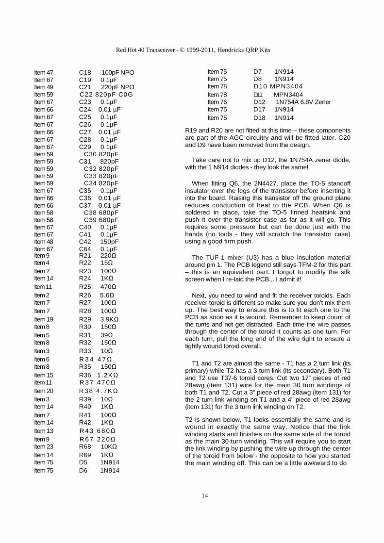
L3 uses a T37-2 toroid core. Cut 14” of red 26awg (item 129) wire and wind 23 turns onto the toroid:
Completed L3
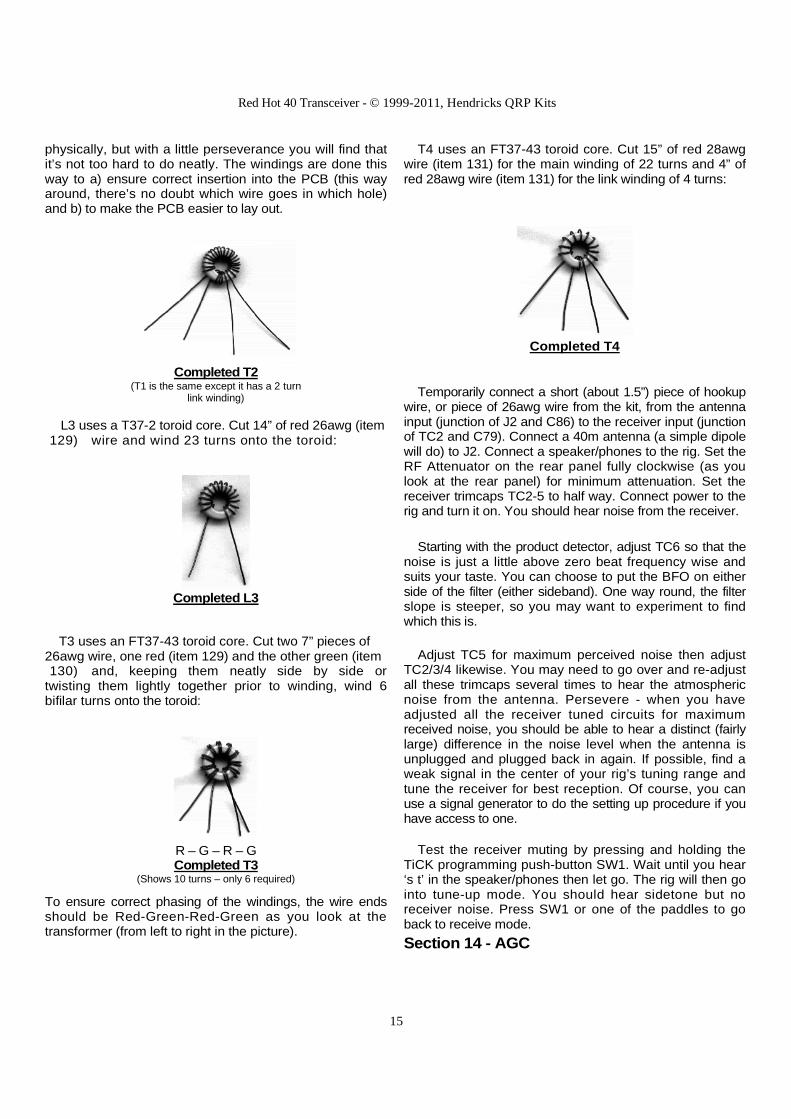
T3 uses an FT37-43 toroid core. Cut two 7” pieces of 26awg wire, one red (item 129) and the other green (item 130) and, keeping them neatly side by side or
twisting them lightly together prior to winding, wind 6 bifilar turns onto the toroid:
R – G – R – G Completed T3
(Shows 10 turns – only 6 required)
To ensure correct phasing of the windings, the wire ends should be Red-Green-Red-Green as you look at the transformer (from left to right in the picture).
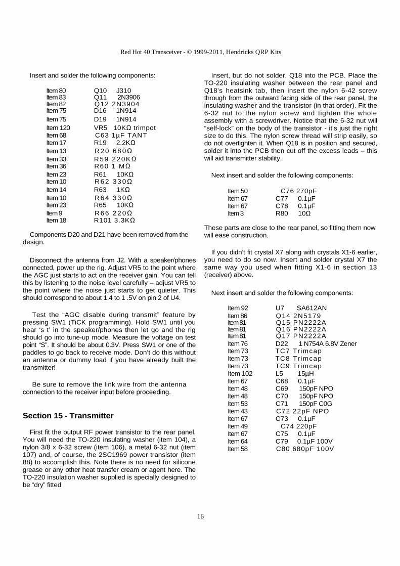
T4 uses an FT37-43 toroid core. Cut 15” of red 28awg wire (item 131) for the main winding of 22 turns and 4” of red 28awg wire (item 131) for the link winding of 4 turns:
Completed T4
Temporarily connect a short (about 1.5”) piece of hookup wire, or piece of 26awg wire from the kit, from the antenna input (junction of J2 and C86) to the receiver input (junction of TC2 and C79). Connect a 40m antenna (a simple dipole will do) to J2. Connect a speaker/phones to the rig. Set the RF Attenuator on the rear panel fully clockwise (as you look at the rear panel) for minimum attenuation. Set the receiver trimcaps TC2-5 to half way. Connect power to the rig and turn it on. You should hear noise from the receiver.
Starting with the product detector, adjust TC6 so that the noise is just a little above zero beat frequency wise and suits your taste. You can choose to put the BFO on either side of the filter (either sideband). One way round, the filter slope is steeper, so you may want to experiment to find which this is.
Adjust TC5 for maximum perceived noise then adjust TC2/3/4 likewise. You may need to go over and re-adjust all these trimcaps several times to hear the atmospheric noise from the antenna. Persevere - when you have adjusted all the receiver tuned circuits for maximum received noise, you should be able to hear a distinct (fairly large) difference in the noise level when the antenna is unplugged and plugged back in again. If possible, find a weak signal in the center of your rig’s tuning range and tune the receiver for best reception. Of course, you can use a signal generator to do the setting up procedure if you have access to one.
Test the receiver muting by pressing and holding the TiCK programming push-button SW1. Wait until you hear ‘s t’ in the speaker/phones then let go. The rig will then go into tune-up mode. You should hear sidetone but no receiver noise. Press SW1 or one of the paddles to go back to receive mode.
Section 14 - AGC
Red Hot 40 Transceiver - © 1999-2011, Hendricks QRP Kits
16
Insert and solder the following components:
Item 80 Q10 J310 Item 83 Q11 2N3906 Item 82 Q12 2N3904 Item 75 D16 1N914 Item 75 D19 1N914 Item 120 VR5 10KΩ trimpot Item 68 C63 1µF TANT Item 17 R19 2.2KΩ Item 13 R 20 68 0Ω Item 33 R59 22 0KΩ Item 36 R60 1 MΩ Item 23 R61 10KΩ Item 10 R 62 33 0Ω Item 14 R63 1KΩ Item 10 R 64 33 0Ω Item 23 R65 10KΩ Item 9 R 66 22 0Ω Item 18 R101 3.3KΩ
Components D20 and D21 have been removed from the design.
Disconnect the antenna from J2. With a speaker/phones connected, power up the rig. Adjust VR5 to the point where the AGC just starts to act on the receiver gain. You can tell this by listening to the noise level carefully – adjust VR5 to the point where the noise just starts to get quieter. This should correspond to about 1.4 to 1 .5V on pin 2 of U4.
Test the “AGC disable during transmit” feature by pressing SW1 (TiCK programming). Hold SW1 until you hear ‘s t’ in the speaker/phones then let go and the rig should go into tune-up mode. Measure the voltage on test point “S”. It should be about 0.3V. Press SW1 or one of the paddles to go back to receive mode. Don’t do this without an antenna or dummy load if you have already built the transmitter!
Be sure to remove the link wire from the antenna connection to the receiver input before proceeding.
Section 15 - Transmitter
First fit the output RF power transistor to the rear panel. You will need the TO-220 insulating washer (item 104), a nylon 3/8 x 6-32 screw (item 106), a metal 6-32 nut (item 107) and, of course, the 2SC1969 power transistor (item 88) to accomplish this. Note there is no need for silicone grease or any other heat transfer cream or agent here. The TO-220 insulation washer supplied is specially designed to be “dry” fitted
Insert, but do not solder, Q18 into the PCB. Place the TO-220 insulating washer between the rear panel and Q18’s heatsink tab, then insert the nylon 6-42 screw through from the outward facing side of the rear panel, the insulating washer and the transistor (in that order). Fit the 6-32 nut to the nylon screw and tighten the whole assembly with a screwdriver. Notice that the 6-32 nut will “self-lock” on the body of the transistor - it’s just the right size to do this. The nylon screw thread will strip easily, so do not overtighten it. When Q18 is in position and secured, solder it into the PCB then cut off the excess leads – this will aid transmitter stability.
Next insert and solder the following components:
Item 50 C76 270pF Item 67 C77 0.1µF Item 67 C78 0.1µF Item 3 R80 10Ω
These parts are close to the rear panel, so fitting them now will ease construction.
If you didn’t fit crystal X7 along with crystals X1-6 earlier, you need to do so now. Insert and solder crystal X7 the same way you used when fitting X1-6 in section 13 (receiver) above.
Next insert and solder the following components:
Item 92 U7 SA612AN Item 86 Q14 2N5179 Item 81 Q15 PN2222A Item 81 Q16 PN2222A Item 81 Q17 PN2222A Item 76 D22 1 N754A 6.8V Zener Item 73 TC7 Trimcap Item 73 TC8 Trimcap Item 73 TC9 Trimcap Item 102 L5 15µH Item 67 C68 0.1µF Item 48 C69 150pF NPO Item 48 C70 150pF NPO Item 53 C71 150pF C0G Item 43 C72 22pF NPO Item 67 C73 0.1µF Item 49 C74 220pF Item 67 C75 0.1µF Item 64 C79 0.1µF 100V Item 58 C80 680pF 100V
Red Hot 40 Transceiver - © 1999-2011, Hendricks QRP Kits
17
Item 52 C81 100pF 100V Item 56 C82 330pF 100V Item 59 C83 820pF 100V Item 54 C84 220pF 100V Item 57 C85 560pF 100V Item 41 C105 4.7pF NPO Item 13 R 70 6 8 0Ω Item 17 R71 2.2KΩ Item 25 R72 15KΩ Item 17 R73 2.2KΩ Item 7 R74 100Ω Item 20 R75 4 .7KΩ Item 15 R76 1.2KΩ Item 4 R77 15Ω Item 4 R78 15Ω Item 5 R 7 9 3 9Ω
Item 121 VR6 500Ω Tr impot
Identify the transmit output filter capacitors carefully - the writing on them is very small - you may need a magnifying glass to make them easier to read. Note also that C79 is a 100V component – it is included separately from the other 37 0.1µF capacitors in the bag. The output filter capacitors are difficult to identify on the silk screen of the PCB as the lettering is so small. To help identify which capacitor goes where, an exploded view of that section of the PCB is available below:
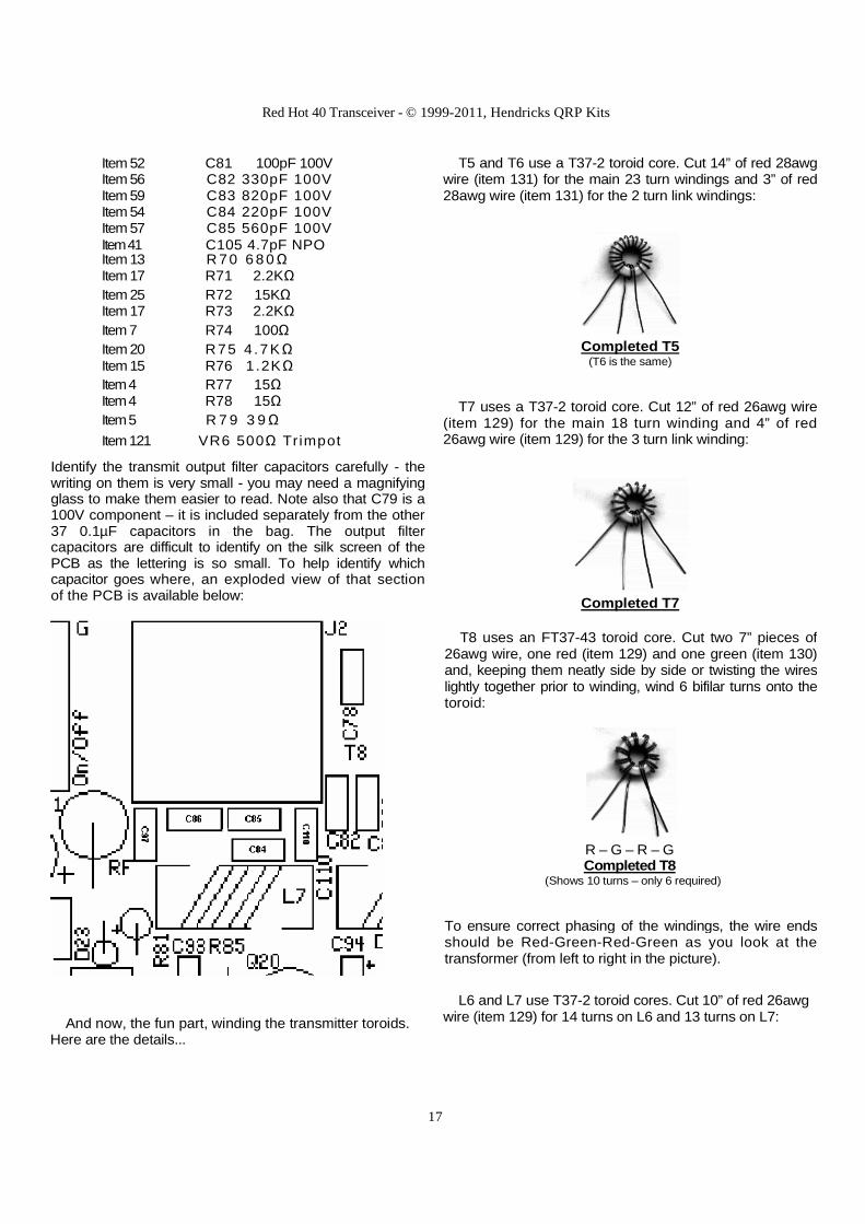
T5 and T6 use a T37-2 toroid core. Cut 14” of red 28awg wire (item 131) for the main 23 turn windings and 3” of red 28awg wire (item 131) for the 2 turn link windings:
Completed T5
(T6 is the same)
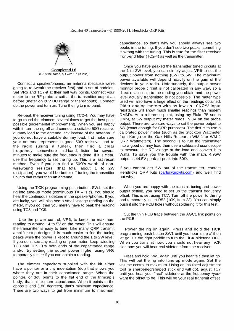
T7 uses a T37-2 toroid core. Cut 12” of red 26awg wire (item 129) for the main 18 turn winding and 4” of red 26awg wire (item 129) for the 3 turn link winding:
Completed T7
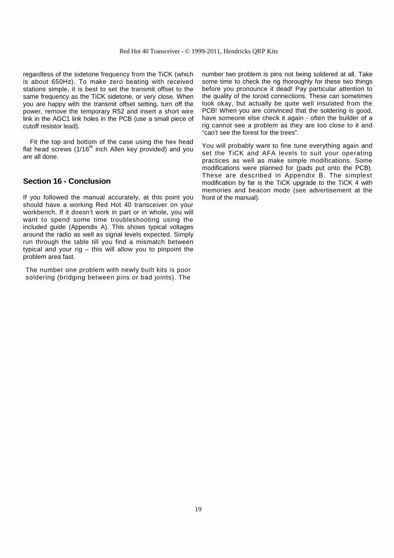
T8 uses an FT37-43 toroid core. Cut two 7” pieces of 26awg wire, one red (item 129) and one green (item 130) and, keeping them neatly side by side or twisting the wires lightly together prior to winding, wind 6 bifilar turns onto the toroid:
R – G – R – G Completed T8
(Shows 10 turns – only 6 required)
To ensure correct phasing of the windings, the wire ends should be Red-Green-Red-Green as you look at the transformer (from left to right in the picture).
And now, the fun part, winding the transmitter toroids. Here are the details...
L6 and L7 use T37-2 toroid cores. Cut 10” of red 26awg wire (item 129) for 14 turns on L6 and 13 turns on L7:
Red Hot 40 Transceiver - © 1999-2011, Hendricks QRP Kits
18
Completed L6
(L7 is the same, but with 1 turn less)
Connect a speaker/phones, an antenna (because we’re going to re-tweak the receiver first) and a set of paddles. Set VR6 and TC7-9 at their half way points. Connect your meter to the RF probe circuit at the transmitter output as before (meter on 20V DC range or thereabouts). Connect up the power and turn on. Tune the rig to mid-band.
Re-peak the receiver tuning using TC2-4. You may have to go round the trimmers several times to get the best peak possible (incremental improvement). When you are happy with it, turn the rig off and connect a suitable 50Ω resistive dummy load to the antenna jack instead of the antenna. If you do not have a suitable dummy load, first make sure your antenna represents a good 50Ω resistive load to the radio (using a tuner), then find a clear frequency somewhere mid-band, listen for several minutes to make sure the frequency is dead. If it is clear, use this frequency to set the rig up. This is a last resort method. Even if you can find a 50Ω’s worth of non-wirewound resistors (that total about 1 to 2W dissipation), you would be better off tuning the transmitter up into that rather than an antenna.
Using the TiCK programming push-button, SW1, set the rig into tune-up mode (continuous TX – ‘s t’). You should hear the continuous sidetone in the speaker/phones. If you are lucky, you will also see a small voltage reading on the meter. If you do, then you merely have to peak the reading using TC8 and TC9.
Use the power control, VR6, to keep the maximum reading to around +4 to 5V on the meter. This will ensure the transmitter is easy to tune. Like many QRP transmit amplifier strip designs, it is much easier to find the tuning peaks while the power is kept to around the 1 to 2W level. If you don’t see any reading on your meter, keep twiddling TC8 and TC9. Try both ends of the capacitance range and/or try setting the output power higher using VR6 temporarily to see if you can obtain a reading.
The trimmer capacitors supplied with the kit either have a pointer or a tiny indentation (dot) that shows you where they are in their capacitance range. When the pointer, or dot, points to the flat end of the trimcap’s body, that’s maximum capacitance. When it points to the opposite end (180 degrees), that’s minimum capacitance. There are two ways to get from minimum to maximum
capacitance, so that’s why you should always see two peaks in the tuning. If you don’t see two peaks, something is wrong with the tuning. This is true for the filter receiver front-end filter (TC2-4) as well as the transmitter.
Once you have peaked the transmitter tuned circuits at the 1 to 2W level, you can simply adjust VR6 to set the output power from nothing (0W) to 5W. The maximum power available will depend heavily on the gain of the devices in your radio. Unfortunately, the output power monitor probe circuit is not calibrated in any way, so a direct relationship to the reading you obtain and the power level actually transmitted is not possible. The meter type used will also have a large effect on the readings obtained. Older analog meters with as low as 10KΩ/V input resistance will show much smaller readings than modern DMM’s. As a reference point, using my Fluke 75 series DMM, at 5W output my meter reads +9.3V on the probe output. There are two sure ways to set the power output to 5W (exact enough for QRP purposes). The first is to use a calibrated power meter (such as the Stockton Wattmeter from Kanga or the Oak Hills Research WM-1 or WM-2 QRP Wattmeters). The second is to run the transmitter into a good dummy load then use a calibrated oscilloscope to measure the RF voltage at the load and convert it to Watts. To save you the trouble with the math, 4.95W output is 44.5V peak-to-peak into 50Ω.
If you cannot get 5W out of the transmitter, contact Hendricks QRP Kits ([email protected]) and we’ll find out why.
When you are happy with the transmit tuning and power output setting, you need to set up the transmit frequency offset. This is set using TC7. Turn off the power to the rig and temporarily insert R52 (10K, Item 23). You can simply push it into the PCB holes without soldering it for this test.
Cut the thin PCB trace between the AGC1 link points on the PCB.
Power the rig on again. Press and hold the TiCK programming push-button SW1 until you hear ‘s t p a’ then let go. Hit the right paddle to turn the TiCK sidetone OFF. When you transmit now, you should not hear any TiCK sidetone: you will hear real sidetone from the receiver.
Press and hold SW1 again until you hear ‘s t’ then let go. This will put the rig into tune-up mode again. Set the volume control to maximum. Using an insulated adjustment tool (a sharpened/shaped stick end will do), adjust TC7 until you hear your “real” sidetone at the frequency *you* want the offset to be. This will be your real transmit offset
Red Hot 40 Transceiver - © 1999-2011, Hendricks QRP Kits
19
regardless of the sidetone frequency from the TiCK (which is about 650Hz). To make zero beating with received stations simple, it is best to set the transmit offset to the same frequency as the TiCK sidetone, or very close. When you are happy with the transmit offset setting, turn off the power, remove the temporary R52 and insert a short wire link in the AGC1 link holes in the PCB (use a small piece of cutoff resistor lead).
Fit the top and bottom of the case using the hex head flat head screws (1/16th inch Allen key provided) and you are all done.
Section 16 - Conclusion
If you followed the manual accurately, at this point you should have a working Red Hot 40 transceiver on your workbench. If it doesn’t work in part or in whole, you will want to spend some time troubleshooting using the included guide (Appendix A). This shows typical voltages around the radio as well as signal levels expected. Simply run through the table till you find a mismatch between typical and your rig – this will allow you to pinpoint the problem area fast.
The number one problem with newly built kits is poor soldering (bridging between pins or bad joints). The
number two problem is pins not being soldered at all. Take some time to check the rig thoroughly for these two things before you pronounce it dead! Pay particular attention to the quality of the toroid connections. These can sometimes look okay, but actually be quite well insulated from the PCB! When you are convinced that the soldering is good, have someone else check it again - often the builder of a rig cannot see a problem as they are too close to it and “can’t see the forest for the trees”.
You will probably want to fine tune everything again and set the TiCK and AFA levels to suit your operating practices as well as make simple modifications. Some modifications were planned for (pads put onto the PCB). These are described in Appendix B. The simplest modification by far is the TiCK upgrade to the TiCK 4 with memories and beacon mode (see advertisement at the front of the manual).
Red Hot 40 Transceiver - © 1999-2011, Hendricks QRP Kits
20
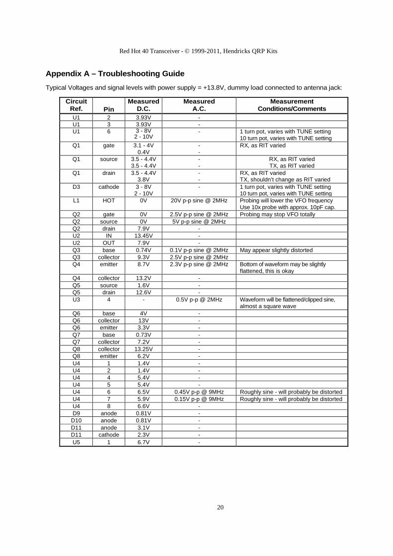
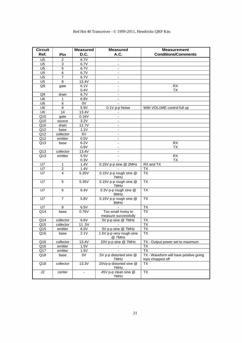
Appendix A – Troubleshooting Guide
Typical Voltages and signal levels with power supply = +13.8V, dummy load connected to antenna jack:
Circuit Ref. Pin
Measured D.C.
Measured A.C.
Measurement Conditions/Comments
U1 2 3.93V - U1 3 3.93V - U1 6 3 - 8V
2 - 10V - 1 turn pot, varies with TUNE setting
10 turn pot, varies with TUNE setting Q1 gate 3.1 - 4V
0.4V - -
RX, as RIT varied
Q1 source 3.5 - 4.4V 3.5 - 4.4V
- -
RX, as RIT varied TX, as RIT varied
Q1 drain 3.5 - 4.4V 3.8V
- -
RX, as RIT varied TX, shouldn’t change as RIT varied
D3 cathode 3 - 8V 2 - 10V
- 1 turn pot, varies with TUNE setting 10 turn pot, varies with TUNE setting
L1 HOT 0V 20V p-p sine @ 2MHz Probing will lower the VFO frequency Use 10x probe with approx. 10pF cap.
Q2 gate 0V 2.5V p-p sine @ 2MHz Probing may stop VFO totally Q2 source 0V 5V p-p sine @ 2MHz Q2 drain 7.9V - U2 IN 13.45V - U2 OUT 7.9V - Q3 base 0.74V 0.1V p-p sine @ 2MHz May appear slightly distorted Q3 collector 9.3V 2.5V p-p sine @ 2MHz Q4 emitter 8.7V 2.3V p-p sine @ 2MHz Bottom of waveform may be slightly
flattened, this is okay Q4 collector 13.2V - Q5 source 1.6V - Q5 drain 12.6V - U3 4 - 0.5V p-p @ 2MHz Waveform will be flattened/clipped sine,
almost a square wave Q6 base 4V - Q6 collector 13V - Q6 emitter 3.3V - Q7 base 0.73V - Q7 collector 7.2V - Q8 collector 13.25V - Q8 emitter 6.2V - U4 1 1.4V - U4 2 1.4V - U4 4 5.4V - U4 5 5.4V - U4 6 6.5V 0.45V p-p @ 9MHz Roughly sine - will probably be distorted U4 7 5.9V 0.15V p-p @ 9MHz Roughly sine - will probably be distorted U4 8 6.6V - D9 anode 0.81V -
D10 anode 0.81V - D11 anode 3.1V - D11 cathode 2.3V - U5 1 6.7V -
Red Hot 40 Transceiver - © 1999-2011, Hendricks QRP Kits
21
Circuit Ref. Pin
Measured D.C.
Measured A.C.
Measurement Conditions/Comments
U5 2 6.7V - U5 3 6.7V - U5 5 6.7V - U5 6 6.7V - U5 7 6.7V - U5 8 13.4V - Q9 gate 6.1V
0.4V - -
RX TX
Q9 drain 6.7V - U6 1 6.8V - U6 6 0V - U6 8 5.9V 0.1V p-p Noise With VOLUME control full up U6 14 13.4V -
Q10 gate 0.16V - Q10 source 3.2V - Q10 drain 12.7V - Q12 base 1.1V - Q12 collector 6V - Q12 emitter 0.5V - Q13 base 6.2V
0.9V - -
RX TX
Q13 collector 13.4V - Q13 emitter 5.5V
0.3V - -
RX TX
U7 1 1.4V 0.15V p-p sine @ 2MHz RX and TX U7 2 1.4V - TX U7 4 5.35V 0.15V p-p rough sine @
7MHz TX
U7 5 5.35V 0.15V p-p rough sine @ 7MHz
TX
U7 6 6.4V 0.3V p-p rough sine @ 9MHz
TX
U7 7 5.8V 0.15V p-p rough sine @ 9MHz
TX
U7 8 6.5V - TX Q14 base 0.76V Too small /noisy to
measure successfully TX
Q14 collector 6.6V 3V p-p sine @ 7MHz TX Q15 collector 11 .5V - TX Q15 emitter 6.0V 3V p-p sine @ 7MHz TX Q16 base 2.1V 1.5V p-p very rough sine
@ 7MHz TX
Q16 collector 13.4V 20V p-p sine @ 7MHz TX - Output power set to maximum Q16 emitter 1.5V - TX Q17 emitter 1.5V - TX Q18 base 0V 5V p-p distorted sine @
7MHz TX - Waveform will have positive going tops chopped off
Q18 collector 13.3V 20Vp-p distorted sine @ 7MHz
TX
J2 center - 45V p-p clean sine @ 7MHz
TX
Red Hot 40 Transceiver - © 1999-2011, Hendricks QRP Kits
22
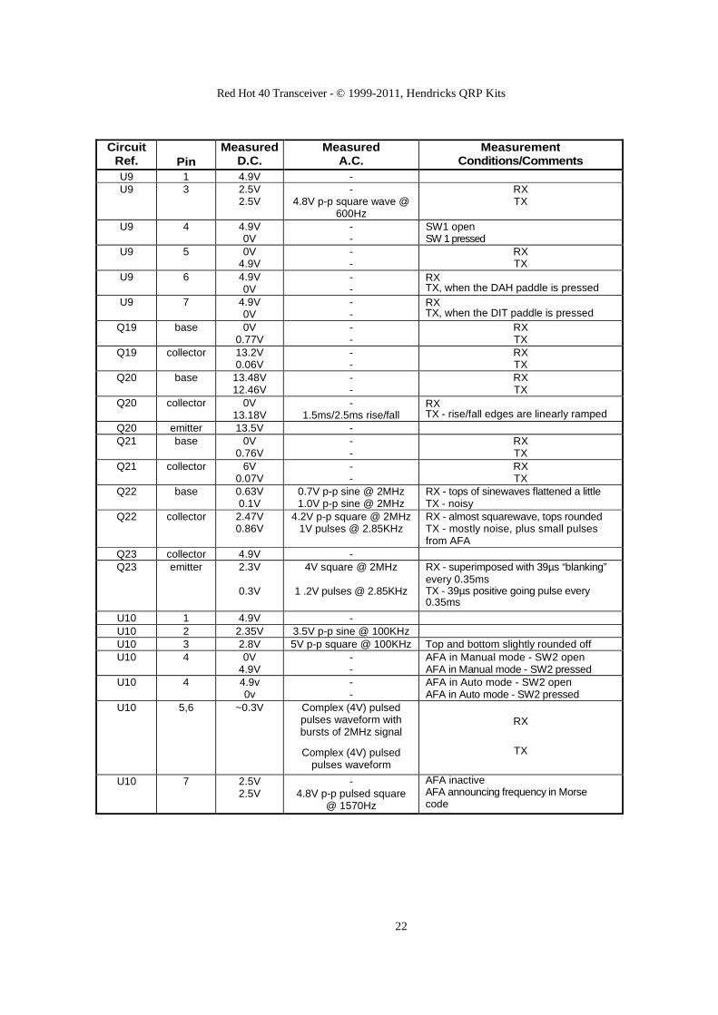
Circuit Ref. Pin
Measured D.C.
Measured A.C.
Measurement Conditions/Comments
U9 1 4.9V - U9 3 2.5V
2.5V -
4.8V p-p square wave @ 600Hz
RX TX
U9 4 4.9V 0V
- -
SW1 open SW 1 pressed
U9 5 0V 4.9V
- -
RX TX
U9 6 4.9V 0V
- -
RX TX, when the DAH paddle is pressed
U9 7 4.9V 0V
- -
RX TX, when the DIT paddle is pressed
Q19 base 0V 0.77V
- -
RX TX
Q19 collector 13.2V 0.06V
- -
RX TX
Q20 base 13.48V 12.46V
- -
RX TX
Q20 collector 0V 13.18V
- 1.5ms/2.5ms rise/fall
RX TX - rise/fall edges are linearly ramped
Q20 emitter 13.5V - Q21 base 0V
0.76V - -
RX TX
Q21 collector 6V 0.07V
- -
RX TX
Q22 base 0.63V 0.1V
0.7V p-p sine @ 2MHz 1.0V p-p sine @ 2MHz
RX - tops of sinewaves flattened a little TX - noisy
Q22 collector 2.47V 0.86V
4.2V p-p square @ 2MHz 1V pulses @ 2.85KHz
RX - almost squarewave, tops rounded TX - mostly noise, plus small pulses from AFA
Q23 collector 4.9V - Q23 emitter 2.3V
0.3V
4V square @ 2MHz
1 .2V pulses @ 2.85KHz
RX - superimposed with 39µs “blanking” every 0.35ms TX - 39µs positive going pulse every 0.35ms
U10 1 4.9V - U10 2 2.35V 3.5V p-p sine @ 100KHz U10 3 2.8V 5V p-p square @ 100KHz Top and bottom slightly rounded off U10 4 0V
4.9V - -
AFA in Manual mode - SW2 open AFA in Manual mode - SW2 pressed
U10 4 4.9v 0v
- -
AFA in Auto mode - SW2 open AFA in Auto mode - SW2 pressed
U10 5,6 ~0.3V Complex (4V) pulsed pulses waveform with bursts of 2MHz signal
Complex (4V) pulsed pulses waveform
RX
TX
U10 7 2.5V 2.5V
- 4.8V p-p pulsed square
@ 1570Hz
AFA inactive AFA announcing frequency in Morse code
Red Hot 40 Transceiver - © 1999-2011, Hendricks QRP Kits
23
Appendix B – Modifications/Experimentation
TiCK upgrade
The Red Hot 40 uses the basic TiCK keyer device. Users may upgrade this to the latest TiCK 4 from Embedded Research easily – the upgrade par t is a drop- in replacement for the TiCK. The TiCK 4 provides extra features such as parameter retention, memories and beacon mode. An order form is provided for your convenience at the front of this manual.
Straight Key Input
There are two ways to run the Red Hot 40 using a straight key. The first is simply to make up a special cable or adapter for your straight key, so that it can be plugged straight into the existing paddle jack socket. The second is to mount another jack socket, that matches your straight key’s jack, on the rear panel (say, just below the existing paddle socket) and wire it to the DIT or DAH input of the TiCK.
There is a test pad labeled ‘K’ on the board where you could connect an external keyer or straight key directly. Grounding this point will cause the Red Hot 40 TX to operate, but will not generate any TiCK sidetone. This method is good for people who want to use external memory keyers with their own built-in sidetone.
Frequency Range
The tuning range of the rig as supplied is about 70KHz. Increasing the value of C5 can further extend the tuning range. This capacitor must be an NPO part.
To make the Red Hot 40 cover the U.S. Novice Band from 7.100 to 7.150MHz, the VFO must be changed to cover the range from 1.850 to 1.900MHz. This can simply be accomplished by adding one or two turns to the VFO coil L1.
VFO output
A clean sine wave VFO output is available from the ‘V’ test point on the board. This output is ideal for feeding LCD frequency displays such as the K1 MG DCC Kit, from Blue Sky Engineering. A coupling capacitor is required to feed this output (not supplied). Use the lowest possible value you can (start with 5pF and work up), to avoid loading the Red Hot 40 VFO circuitry.
XIT/RIT
Although the Red Hot 40 only has RIT as standard, it is a relatively simple matter to add a switch to allow selection of RIT/OFF/XIT. The switch required is a simple SPST with center OFF position. To do this modification, cut the XIT mod-track on the underside of the board. Then, take two wires from the XIT holes and a third from the test point marked ‘T’ on the board (sheet 5 of the schematic). These three wires go to the switch. Voila, it’s done.
Data Modes
The Red Hot 40 can be modified quite simply to add RTTY or other data modes. Since the rig is varicap diode tuned and the varicap is fed by a summing op-amp, any FSK offset you desire (positive or negative) can be had by feeding the appropriate voltage to the ‘D’ test point on the board - via a resistor to set the gain of course. You will need to devise some circuitry for the interface here.
Received audio for data recovery is available from the ‘A’ test point on the board – PCB traces are provided to add a miniature trimpot to vary the fixed audio output level (next to VR4) labeled “Trimpot” and either a resistor or a capacitor in the position labeled “R/C”. The constructor will have to supply these parts.
Internal Loudspeaker
It is possible to use an internal loudspeaker with the Red Hot 40. You have to convince yourself first that you want to drill holes in the top of your nice new anodized case! If you do decide to do this, care and attention should be paid to the effect that the magnetic field of the chosen loudspeaker will have on the tuned circuits (toroids) in the rig. It is recommended that the user pay due diligence by experimenting with the chosen loudspeaker before drilling holes in the rig’s top! I found a 3” low profile 8Ω 0.8W speaker that fitted perfectly. The only effect it had on the circuitry was to lower the VFO frequency a couple of KHz. Your mileage may vary – experiment before drilling holes.
Headphones
Some users will notice high frequency hiss when using sensitive hi-fi type earphones plugged directly into the loudspeaker jack socket. This is due to the LM380 audio
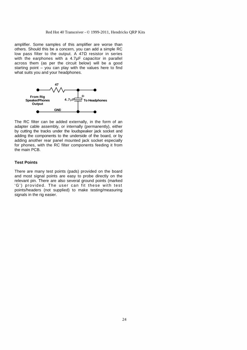
Red Hot 40 Transceiver - © 1999-2011, Hendricks QRP Kits
24
amplifier. Some samples of this amplifier are worse than others. Should this be a concern, you can add a simple RC low pass filter to the output. A 47Ω resistor in series with the earphones with a 4.7µF capacitor in parallel across them (as per the circuit below) will be a good starting point – you can play with the values here to find what suits you and your headphones.
The RC filter can be added externally, in the form of an adapter cable assembly, or internally (permanently), either by cutting the tracks under the loudspeaker jack socket and adding the components to the underside of the board, or by adding another rear panel mounted jack socket especially for phones, with the RC filter components feeding it from the main PCB.
Test Points
There are many test points (pads) provided on the board and most signal points are easy to probe directly on the relevant pin. There are also several ground points (marked ‘G ’ ) prov ided. The user can f i t these wi th tes t points/headers (not supplied) to make testing/measuring signals in the rig easier.
47Ω
From Rig Speaker/Phones
Output 4.7µF __
GND
To Headphones
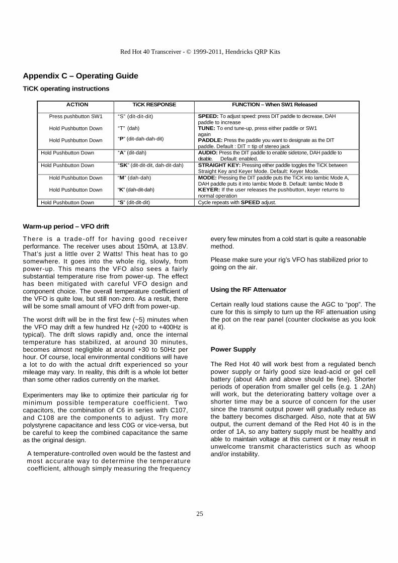
Red Hot 40 Transceiver - © 1999-2011, Hendricks QRP Kits
25
Appendix C – Operating Guide
TiCK operating instructions
ACTION TiCK RESPONSE FUNCTION – When SW1 Released
Press pushbutton SW1
Hold Pushbutton Down
Hold Pushbutton Down
“S” (dit-dit-dit)
“T” (dah)
“P” (dit-dah-dah-dit)
SPEED: To adjust speed: press DIT paddle to decrease, DAH paddle to increase TUNE: To end tune-up, press either paddle or SW1 again PADDLE: Press the paddle you want to designate as the DIT paddle. Default : DIT = tip of stereo jack
Hold Pushbutton Down “A” (dit-dah) AUDIO: Press the DIT paddle to enable sidetone, DAH paddle to disable. Default: enabled.
Hold Pushbutton Down “SK” (dit-dit-dit, dah-dit-dah) STRAIGHT KEY: Pressing either paddle toggles the TiCK between Straight Key and Keyer Mode. Default: Keyer Mode.
Hold Pushbutton Down
Hold Pushbutton Down
“M” (dah-dah)
“K” (dah-dit-dah)
MODE: Pressing the DIT paddle puts the TiCK into Iambic Mode A, DAH paddle puts it into Iambic Mode B. Default: Iambic Mode B KEYER: If the user releases the pushbutton, keyer returns to normal operation
Hold Pushbutton Down “S” (dit-dit-dit) Cycle repeats with SPEED adjust.
Warm-up period – VFO drift
There is a t rade-of f for hav ing good receiver performance. The receiver uses about 150mA, at 13.8V. That’s just a little over 2 Watts! This heat has to go somewhere. It goes into the whole rig, slowly, from power-up. This means the VFO also sees a fairly substantial temperature rise from power-up. The effect has been mitigated with careful VFO design and component choice. The overall temperature coefficient of the VFO is quite low, but still non-zero. As a result, there will be some small amount of VFO drift from power-up.
The worst drift will be in the first few (~5) minutes when the VFO may drift a few hundred Hz (+200 to +400Hz is typical). The drift slows rapidly and, once the internal temperature has stabilized, at around 30 minutes, becomes almost negligible at around +30 to 50Hz per hour. Of course, local environmental conditions will have a lot to do with the actual drift experienced so your mileage may vary. In reality, this drift is a whole lot better than some other radios currently on the market.
Experimenters may like to optimize their particular rig for minimum possible temperature coeffic ient. Two capacitors, the combination of C6 in series with C107, and C108 are the components to adjust. Try more polystyrene capacitance and less C0G or vice-versa, but be careful to keep the combined capacitance the same as the original design.
A temperature-controlled oven would be the fastest and most accurate way to determine the temperature coefficient, although simply measuring the frequency
every few minutes from a cold start is quite a reasonable method.
Please make sure your rig’s VFO has stabilized prior to going on the air.
Using the RF Attenuator
Certain really loud stations cause the AGC to “pop”. The cure for this is simply to turn up the RF attenuation using the pot on the rear panel (counter clockwise as you look at it).
Power Supply
The Red Hot 40 will work best from a regulated bench power supply or fairly good size lead-acid or gel cell battery (about 4Ah and above should be fine). Shorter periods of operation from smaller gel cells (e.g. 1 .2Ah) will work, but the deteriorating battery voltage over a shorter time may be a source of concern for the user since the transmit output power will gradually reduce as the battery becomes discharged. Also, note that at 5W output, the current demand of the Red Hot 40 is in the order of 1A, so any battery supply must be healthy and able to maintain voltage at this current or it may result in unwelcome transmit characteristics such as whoop and/or instability.
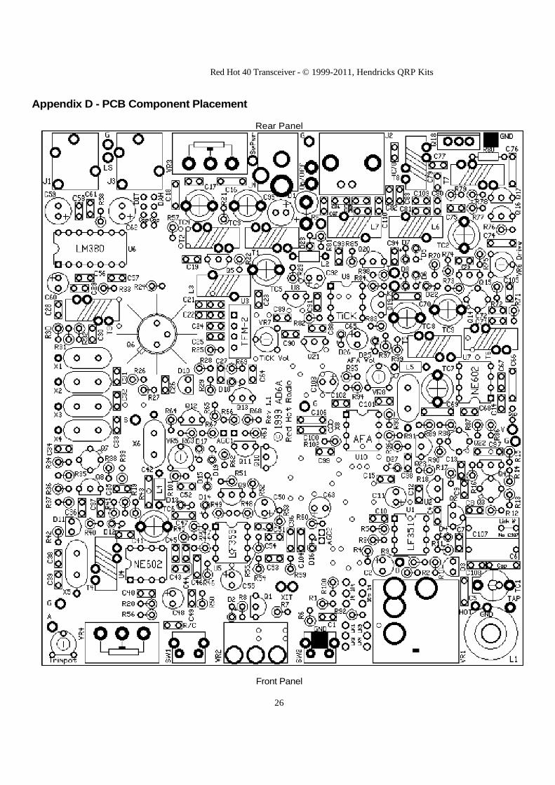
Red Hot 40 Transceiver - © 1999-2011, Hendricks QRP Kits
Appendix D - PCB Component Placement
Rear Panel
Front Panel
26
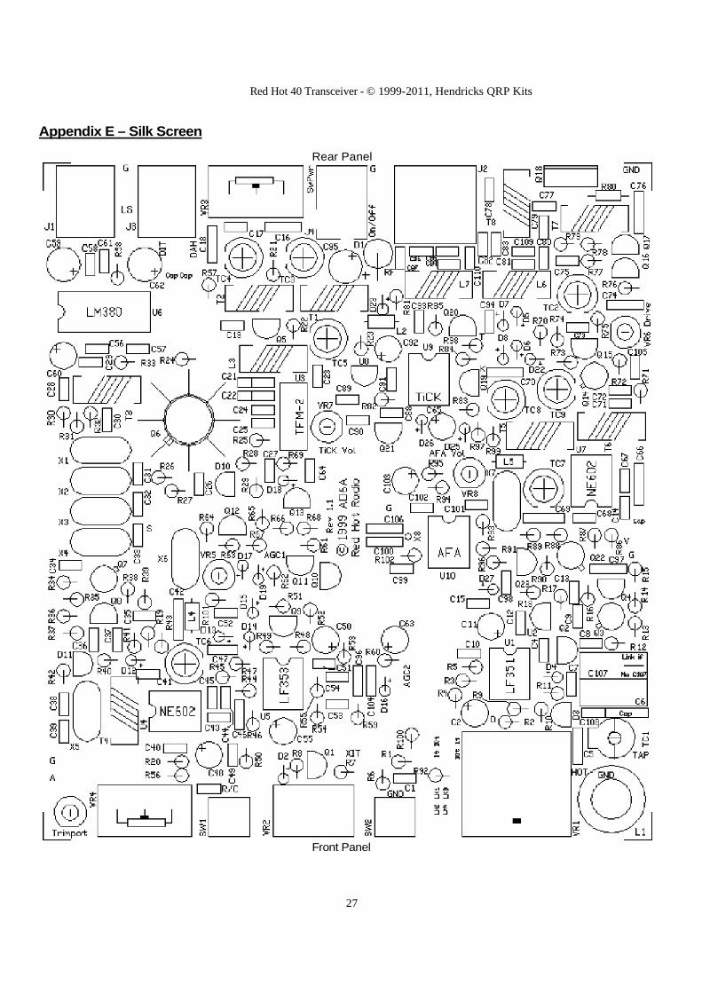
Red Hot 40 Transceiver - © 1999-2011, Hendricks QRP Kits
27
Appendix E – Silk Screen
Rear Panel
Front Panel
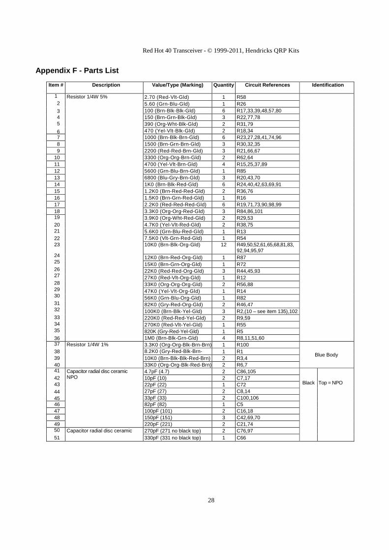
Red Hot 40 Transceiver - © 1999-2011, Hendricks QRP Kits
28
Appendix F - Parts List
Item # Description Value/Type (Marking) Quantity Circuit References Identification
1
2
3
4
5
6
Resistor 1/4W 5% 2.70 (Red-Vlt-Gld) 1 R58 5.60 (Grn-Blu-Gld) 1 R26
100 (Brn-Blk-Blk-Gld) 6 R17,33,39,48,57,80
150 (Brn-Grn-Blk-Gld) 3 R22,77,78
390 (Org-Wht-Blk-Gld) 2 R31,79
470 (Yel-Vlt-Blk-Gld) 2 R18,34
7 1000 (Brn-Blk-Brn-Gld) 6 R23,27,28,41,74,96
8 1500 (Brn-Grn-Brn-Gld) 3 R30,32,35
9 2200 (Red-Red-Brn-Gld) 3 R21,66,67
10 3300 (Org-Org-Brn-Gld) 2 R62,64
11 4700 (Yel-Vlt-Brn-Gld) 4 R15,25,37,89
12 5600 (Grn-Blu-Brn-Gld) 1 R85
13 6800 (Blu-Gry-Brn-Gld) 3 R20,43,70
14 1K0 (Brn-Blk-Red-Gld) 6 R24,40,42,63,69,91
15 1.2K0 (Brn-Red-Red-Gld) 2 R36,76
16 1.5K0 (Brn-Grn-Red-Gld) 1 R16
17 2.2K0 (Red-Red-Red-Gld) 6 R19,71,73,90,98,99
18 3.3K0 (Org-Org-Red-Gld) 3 R84,86,101
19
20
21
22
23
24
25
26
27
28
29
30
31
32
33
34
35
36
3.9K0 (Org-Wht-Red-Gld) 2 R29,53
4.7K0 (Yel-Vlt-Red-Gld) 2 R38,75
5.6K0 (Grn-Blu-Red-Gld) 1 R13
7.5K0 (Vlt-Grn-Red-Gld) 1 R54
10K0 (Brn-Blk-Org-Gld) 12 R49,50,52,61,65,68,81,83,
92,94,95,97
12K0 (Brn-Red-Org-Gld) 1 R87
15K0 (Brn-Grn-Org-Gld) 1 R72
22K0 (Red-Red-Org-Gld) 3 R44,45,93
27K0 (Red-Vlt-Org-Gld) 1 R12
33K0 (Org-Org-Org-Gld) 2 R56,88
47K0 (Yel-Vlt-Org-Gld) 1 R14
56K0 (Grn-Blu-Org-Gld) 1 R82
82K0 (Gry-Red-Org-Gld) 2 R46,47
100K0 (Brn-Blk-Yel-Gld) 3 R2,(10 – see item 135),102
220K0 (Red-Red-Yel-Gld) 2 R9,59
270K0 (Red-Vlt-Yel-Gld) 1 R55
820K (Gry-Red-Yel-Gld) 1 R5
1M0 (Brn-Blk-Grn-Gld) 4 R8,11,51,60
37
38
39
40
Resistor 1/4W 1% 3.3K0 (Org-Org-Blk-Brn-Brn) 1 R100
Blue Body
8.2K0 (Gry-Red-Blk-Brn-Brn)
1 R1
10K0 (Brn-Blk-Blk-Red-Brn) 2 R3,4
33K0 (Org-Org-Blk-Red-Brn) 2 R6,7
41
42
43
44
45
Capacitor radial disc ceramic
NPO
4.7pF (4.7) 2 C86,105
Black Top = NPO
10pF (10) 2 C7,17
22pF (22) 1 C72
27pF (27) 2 C8,14
33pF (33) 2 C100,106
46 82pF (82) 1 C5
47 100pF (101) 2 C16,18
48 150pF (151) 3 C42,69,70
49 220pF (221) 2 C21,74
50
51
Capacitor radial disc ceramic 270pF (271 no black top) 2 C76,97
330pF (331 no black top) 1 C66
Red Hot 40 Transceiver - © 1999-2011, Hendricks QRP Kits
29
52 Capacitor radial ceramic C0G 100V 5%
1 00pF (101) 1 C81 53
54 55 56 57
150pF (151) 1 C71 220pF (221) 1 C84 270pF (271) 1 C108 330pF (331) 1 C82 560pF (561) 1 C85
58 680pF (681) 3 C38,39,80 59 820pF (821) 7 C22,30,31 ,32,33,34,83 60 Capacitor axial polystyrene 5% 1 80pF (1 80J) 1 C6
Clear Body
61 Capacitor radial polyester film 100V 10%
1000pF (102) 2 C96,104 Green Body
62 1500pF (152) 2 C46,47 63 Capacitor radial ceramic X7R 0.047µF (473) 1 C43
64 Capacitor radial X7R 100V 10% 0.1µF (104) 1 C79
65 Capacitor Z5U 50V 20% 0.22µF (224) 1 C52 66 Capacitor axial X7R 50V 10% 0.01µF (103) 11 C24,27,36,37,53,54,
57,88,89,99, 101
67 Capacitor axial X7R 50V 10% 0.1µF (104) 37 C1,4,9,10,12,13,15,19,23, 25,26,28,29,35,40,41,44, 45,49,51,56,58,61,64,67, 68,73,75,77,78,87,90,91, 93,94,98,102
68 Capacitor radial tantalum bead 35V
1µF (1, 35V) 1 C63 1+ 35
69 Capacitor radial elec alum 16V 4.7µF 16V 2 C55,60 70 Capacitor radial elec alum 16V 10µF 16V 7 C2,11,48,50,65,92,103
71 Capacitor radial elec alum 16V 100µF 16V 3 C59,62,95 72 Ceramic trimmer capacitor 15 - 50pF (orange) 1 TC1
73 Ceramic trimmer capacitor 8 - 50pF (brown) 8 TC2,3,4,5,6,7,8,9
74 3A Schottky Diode 1 N5822 1 D1 _________ +
75 General purpose small signal diode
1N914 17 D2,4,5,6,7,8,13,14,15,16, 17,18,19,23,25,26,27 +
76 Zener diode 6.8V 400mW 1 N754A 2 D1 2,22 77 Varicap diode, TO92 MV209 1 D3 78 PIN Diode, TO92 MPN3404 2 D10,11
79 JFET, TO92 2N5457 2 Q1,9 80 JFET, TO92 J310 3 Q2,5,10 81 NPN GP transistor, TO92 PN2222A 4 Q4,15,16,17 82 NPN GP transistor, TO92 2N3904 6 Q8,12,13,19,21,23 83 PNP GP transistor, TO92 2N3906 2 Q1 1,20 84 Voltage reg.+8V 100mA, TO92 L78L08ACZ 1 U2 85 Voltage reg.+5V 1 00mA, TO92 LM78L05 1 U8 86 NPN RF transistor, TO72 2N5179 4 Q3,7,14,22
Red Hot 40 Transceiver - © 1999-2011, Hendricks QRP Kits
30
87 NPN medium power RF transistor, TO39
2N4427 1 Q6
88 NPN RF power transistor, TO220 2SC1969 1 Q18
89 Minicircuits +7dBm mixer, B02
case TUF-1 1 U3
90 GP single op-amp, 8-pin DIL LF351N 1 U1 91 GP dual op-amp, 8-pin DIL LF353N 1 U5 92 Double-balanced mixer/oscillator,
8-pin DIL NE602AN/SA61 2AN (either) 2 U4,7
93 Programmable keyer, 8-pin DIL TICK Rev.1 .02 (white label) 1 U9 94 Audible Frequency Annunciator
(AFA-40), 8-pin DIL 12C508A 1 U10
95 Audio amplifier 2W, 14-pin DIL LM380N 1 U6
96 Crystal AT cut fundamental, HC- 49/u
9.000MHz 7 X1 ,2,3,4,5,6,7
97 Crystal, C-2 type 100KHz 1 X8 98 99 100 101
Toroid core T50-7 (White) 1 L1 T37-6 (Yellow) 2 T1 ,2 T37-2 (Red) 6 L3,6,7 & T5,6,7 FT37-43 (Plain - dark grey) 3 T3,4,8
102
103
Miniature RFC 15uH (Brn-Grn-Blk-Gld) 2 L4,5 12uH (Brn-Red-Blk-Gld) 1 L2
104 TO-220 insulating washer 1 105 TO-5 transistor standoff insulator
for Q6 (white nylon disc) 1
106 Nylon screw (for Q1 8) 6-32 x 3/8' 1 107 Metal nut for nylon screws 6-32 Nut 2 108 Large solder lug for front panel
ground 0.4' ID 1 Fits on RIT pot VR2
109 Solder lug (rear panel ground) 1 Cut Here
. 110 Screw (solder lug ground) 4-40 x 0.25' 1 111 Nut for screw (solder lug ground) 4-40 Nut 1 112 Fiber shoulder washer for L1 2
113 Nylon screw for L1 6-32 x 5/8' 1 114 Screws for assembling box -
countersunk 4-40 x 0.25' black, hex socket head
8 1/16”allen key supplied with kit
115 PCB - double sided, plated
through, solder masked 1
116 Box (4 pieces) 1
Red Hot 40 Transceiver - © 1999-2011, Hendricks QRP Kits
31
117 Push-button switch TL1105S 2 SW1,2 118 Potentiometer, min., 17mm, PCB 10K 2 VR3,4 119 Potentiometer, min.,16mm,
center detent 10K 1 VR2
120 Potentiometer, 6mm, carbon trimmer (trim pot)
10K 3 VR5,7,8 121 Potentiometer, 6mm, carbon
trimmer (trim pot) 500R 1 VR6
122 Potentiometer, 10 turn precision 10K 1 VR1 123 Knob, black for TUNE control 1.39' dia. 1 124 Knob, black for RIT, AF & RF
controls 0.77' dia. 3
125 Power jack (socket) PCB mount, NC switch
2.5mm 1 J4 126 BNC socket with lock ring and
panel nut 50 Ohm BNC 1 J2
127 Stereo jack socket, switched, with panel nut (ring)
3.5mm 2 J1,3 128 Finned Heatsink for Q18 (push-
on) TO-5 1
129 Magnet wire - NYSOL, red 26awg 10 feet Toroid inductors 130 Magnet wire - NYSOL, green 26awg 10 feet Toroid inductors 131 Magnet wire – NYSOL, red 28awg 10 feet Toroid inductors 132 Stick-on rubber feet for case 3M 4 133 DIL socket, gold turned pin 8 pin 2 For use on U9 and U10 134 Power cord 6’ x 18awg with moulded
2.5mm power plug 1
135 Inductor RFC 82µH (Gry-Red-Blk-Gld) 1 Use instead of R10 (was 10KΩ) – see text on page 9


