PROGRAMME THURSDAY Location: (Graphene/Materials for Energy) Chair: David Moran (Nanomaterials/Soft Matter) Chair: Gilberto Teobaldi 6 DEC 12 0900-0950 0950-1000 Registration and Breakfast Arrival of Guests-of-Honour Cinzia Casiraghi Jim Yang Lee Alan Partridge (Rolls Royce) Teabreak Ned J. Ekins-Daukes Chaim Sing Yang Jamie Warner End Reception for Speakers and Invited Guests Wang Junling Chong Kim Ong Mark Platt Teabreak Melvin Zin (3M) Gregory Chass Christian Kloc 1015-1020 1020-1030 1030-1045 1045-1120 1120-1155 1155-1230 1230-1330 1330-1415 1415-1445 1445-1515 1515-1545 1545-1600 1600-1630 1630-1700 1700-1730 1730 1800 Welcome Address by Organizers Address by British High Commissioner Address by Minister of State for Trade and Industry Lunch / Poster session Poster Judging KEYNOTE TALK: PERSPECTIVES ON FERROELECTRICS AND MULTIFERROICS James Scott , University of Cambridge Chair: Lee Pooi See, Nanyang Technological University KEYNOTE TALK: NANOBIOMATERIALS: HOW USEFUL ARE THEY? Subbu Venkatraman, Nanyang Technological University Chair: Cleo Choong, Nanyang Technological University KEYNOTE TALK: NEW DIRECTIONS IN MATERIALS SCIENCE AND TECHNOLOGY: TWO-DIMENSIONAL CRYSTALS Antonio Castro Neto, National University of Singapore Chair: Sow Chorng Haur, National University of Singapore PROGRAMME FRIDAY (Graphene/Materials for Energy) Chair: Cinzia Casiraghi (Nanomaterials/Soft Matter) Chair: Gregory Chass 7 Dec 12 0830-0900 Registration and Breakfast Zhang Hua David Moran Chen Xiaodong Richard Kwok (ST Kinetics) Qi Xiaoying Lunch Onsite Discussion Lab Visits (NTU / NUS) for invited speakers and collaborators only End Reception for Speakers and Invited guests Rob Aitken (IOM) Andrew Dove Sow Chorng Haur Gilberto Teobaldi Christian Nijhuis 0900-0935 0935-0940 0940-1010 1010-1040 1040-1110 1110-1140 1140-1210 1210-1310 1310-1500 1500-1700 1700 1800 Poster competition Prize presentation KEYNOTE TALK: CARBON MATERIALS FOR QUANTUM TECHNOLOGIES Andrew Briggs, University of Oxford Chair: Andrew Wee, National University of Singapore Location: BREAKTHROUGH CREATION BREAKTHROUGH Location: BREAKTHROUGH Location: BREAKTHROUGH CREATION 1 2
Welcome Address by OrganizersAddress by British High CommissionerAddress by Minister of State for Trade and Industry
Lunch / Poster sessionPoster Judging
KEYNOTE TALK: PERSPECTIVES ON FERROELECTRICS AND MULTIFERROICSJames Scott , University of CambridgeChair: Lee Pooi See, Nanyang Technological UniversityKEYNOTE TALK: NANOBIOMATERIALS: HOW USEFUL ARE THEY?Subbu Venkatraman, Nanyang Technological UniversityChair: Cleo Choong, Nanyang Technological University
KEYNOTE TALK: NEW DIRECTIONS IN MATERIALS SCIENCE AND TECHNOLOGY: TWO-DIMENSIONAL CRYSTALSAntonio Castro Neto, National University of SingaporeChair: Sow Chorng Haur, National University of Singapore
LunchOnsite DiscussionLab Visits (NTU / NUS) for invited speakers and collaborators onlyEndReception for Speakers and Invited guests
Rob Aitken (IOM)Andrew Dove
Sow Chorng HaurGilberto TeobaldiChristian Nijhuis
0900-0935
0935-0940
0940-10101010-10401040-11101110-11401140-1210
1210-13101310-15001500-170017001800
Poster competition Prize presentation
KEYNOTE TALK: CARBON MATERIALS FOR QUANTUM TECHNOLOGIESAndrew Briggs, University of OxfordChair: Andrew Wee, National University of Singapore
Location: BREAKTHROUGH CREATION
BREAKTHROUGH
Location: BREAKTHROUGH
Location: BREAKTHROUGH CREATION
1 2
James Scott is a member of the Physics Department at Cambridge University, where he serves as a Director of Research.
Prof. Scott was elected FRS (physics) in May 2008. His citation refers to him as "the father of integrated ferroelectrics," which are ferroelectric crystal memory thin films attached to silicon or GaAs computer chips.
Prof. Scott was awarded the Materials Research Society (MRS) gold medal in December 2008 "for fundamental contributions to the materials science of oxides underlying current and futureelectronic devices", and the Jozef Stefan Medal from Slovenia in March 2009 (previous recipients include Nobel Prize-winners P.-G. DeGennes and Abdus Salam.)
Of the 20 Top Papers selected each year by the editors of the Journal of Physics Condensed Matter, Prof. Scott was author of 3 in 2008 and 2 in 2007 - one-eighth of the worldwide two-year total. Other publications in high-impact journals 2007-9: Physical Review Letters (5); Nature/Nature Materials (6); Science (1).
Scott's book "Ferroelectric Memories" (Springer 2000) has completely sold out its first edition print-run (800 copies @ £100), and the Chinese (Tsinghua Press, 2004) and Japanese (Springer- Japan, 2003) translations are selling well. With 2950 citations, it is the most cited text on ferroelectricity.
In 2011 he was elected to the Slovenia Academy of Sciences.
PERSPECTIVES ON FERROELECTRICS AND MULTIFERROICS
Professor J. F. ScottDirector of Research, Department of Physics,Cavendish Laboratory Cambridge University
I will present an overview of the most popular topics in the field of dielectrics, emphasizing new photovoltaic studies, new kinds ofresistive random access memories (RRAMs), room- temperature magnetoelectric multiferroics, and unexpected nanodomain structures.
PERSPECTIVES ON FERROELECTRICS AND MULTIFERROICS
3 4
Professor, Materials Science and Engineering, Nanyang Technological University, N4.1-1-30, Nanyang Avenue, Singapore 639798, July 2000-present
Acting Chair, School of Materials Science and Engineering, June 2012 - present Director, Biomedical Engineering Research Centre, NTU, January 2007-present. Director, Ocular Therapeutic Engineering Centre, April 2012 – present
Deputy Director (Graduate Studies), Nanyang Institute of Technology in Health and Medicine (NITHM), April 2012 - present
NANOBIOMATERIALS: HOW USEFUL ARE THEY?
Professor Subbu VenkatramanSchool of Materials Science & Engineering, Nanyang Technological University, Singapore
There has been substantial buzz about nanobiomaterials in the scientific literature for the past decade. Broadly speaking, nanobiomaterials have been considered for drug delivery, in vivo imaging, in vitro diagnostics and less convincingly, for engineering of soft tissue. In this talk, I will give an overview of the work in these four areas, with emphasis on the NTU efforts. We have developed several nanocarriers for drug and gene delivery, particularly liposomes and erythrocyte-derived carriers. Our Centre for Biomimetic Sensor Science has been focusing on polymerosomes not only for diagnostic applications, but also for mimicking cellular function; such understanding will enable us eventually to design synthetic “protocells” that may play an interesting role in tissue engineering. In in vivo imaging, the thrust is on developing nanoparticles that localize or can be made to localize in selected tissues, to enhance contrast and resolution in MRI and ultrasound imaging. Finally, in the area of soft tissue engineering, there is considerable effort in studying nanopatterns for guiding cellular growth and proliferation on biomaterial surfaces. In specific situations, there are indications that cells do respond to such patterns, occasionally also in 3-dimensional systems. Our work on nanostructuring in hydrogels will be presented as an example of how cell growth is influenced in 3-D systems.
NANOBIOMATERIALS: HOW USEFUL ARE THEY?
Subbu Venkatraman obtained his Bachelor’s and Master’s degrees from India, then a PhD in Polymer Science from Carnegie-Mellon University, Pittsburgh. Following a post-doctoral fellowship at University of Pittsburgh, he was hired into the R&D organization of Raychem Corporation in California. He then went on to specialize in drug delivery research at two leading biotech companies, before joining NTU in 2000. He is the author of over 135 manuscripts and about 15 patents and another 15 patent applications worldwide. He is also the co-founder of three companies, Amaranth Medical, CardioRev and AdComp Therapeutics, specializing in therapeutic medical devices and drug delivery products. He also won the Nanyang Award for Innovation in 2012, on the strength of his patented work on cardiovascular implants. He has been awarded the Competitive Research Programme (CRP) grant (worth $10MM), co-awarded the NTU-Technion Create grant (~$20MM) as well as several proof-of-concept grants totaling about $2MM. In addition he is a key technology contributor to the Singapore Eye Research institute’s Translational Clinical Research (TCR) programme. Three of his prototypes are ready to go into human trials shortly.
Luo, R., Mutukumaraswamy, S., Venkatraman, S.S., Neu, B. Engineering of erythrocyte-based drug carriers: control of protein release and bioactivity, Journal of Materials Science: Materials in Medicine , 23 (1), pp. 63-71 (2012)X. Y. Qi, X. Huang, H. Li, Y. S. Wang, Y. Xia, M. Natarajan, J. Wei, S. S. Venkatraman, H. Zhang*: “Vault Protein-Templated Assembles of Nanoparticles”, ACS NANO, 791), pp.1250001-7 (2012).Tay Chor Yong, Scott Irvine, Freddy Boey, Lay Poh Tan and Subbu Venkatraman, Micro-nanoengineered Cellular Responses for Soft Tissue Engineering, Small (special issue), 7, 1361-1378 (2011)Tay CY, Pal M, Yu H, Leong WS, Tan NS, Ng KW, Venkatraman S, Boey F, Leong DT, Tan LP, Bio-inspired micropatterned platform to steer stem cell differentiation., Small, 10, 1416-1421 (2011).Xia, Y., Ramgopal, Y., Li, H., Shang, L., Srinivas, P., Kickhoefer, V.A., Rome, L.H., Preiser, P.R., Boey, F., Zhang, H., Venkatraman, S.S., Immobilization of recombinant vault nanoparticles on solid substrates, ACS Nano, 4(3), 1417-1424 (2010)Lihong Liu, Kaijin Xu, Huaying Wang, P. K. Jeremy Tan, Weimin Fan, Subbu S. Venkatraman, Lanjuan Li, Yi-Yan Yang , Self-assembled cationic peptide nanoparticles as an efficient antimicrobial agent, Nature Nanotechnology 4, 457-463 (28 June 2009) doi:10.1038/nnano.2009.153
Selected Publications:
[1]
[2]
[3]
[4]
[5]
[6]
5 6
Professor A. H. Castro Neto got his Ph.D. in Physics at University of Illinois at Urbana- Champaign in 1994. In 1994, he moved to the Institute for Theoretical Physics at the University of California at Santa Barbara as a postdoctoral fellow. In 1995, he became an Assistant Professor at University of California at Riverside. In 2000, he moved to Boston University as Professor of Physics. At Boston, Prof. Castro Neto became one of the leading theorists in the study of graphene. In 2010, Prof. Castro Neto became the Director of the Graphene Research Center and Distinguished Professor at the National University of Singapore.
In 2003, Prof. Castro Neto was elected a fellow of the American Physical Society. He is the colloquia Editor for Reviews of Modern Physics, and co-editor for Europhysics Letters. Prof. Castro Neto was awarded the 11th Ross J. Martin Award by the University of Illinois at Urbana-Champaign, the University of California Regent Fellowship, the Alfred P. Sloan Research Fellowship, the visiting Miller Professorship by the University of California, Berkeley, the visiting Gordon Godfrey Professorship by the University of New South Wales, Australia, and the Distinguished Visiting Chair Professor at the SKKU Advanced Institute of Nano-Technology (SAINT), South Korea. Prof. Castro Neto has authored more than 200 manuscripts and has published in prestigious journals including Science, Nature Materials, Nature Physics, and Physical Review Letters, and has over 12,000 citations. Prof. Castro Neto has given more than 200 seminars worldwide.
NEW DIRECTIONS IN MATERIALS SCIENCE AND TECHNOLOGY: TWO-DIMENSIONAL CRYSTALS
Professor Antonio H. Castro NetoDirector, Graphene Research Centre National University of Singapore, Singapore Professor of Physics, Boston University, USA
Smart advanced materials that are flexible (for transparent wearable electronics), adaptable (that change structure depending on exterior conditions), multifunctional (that can be tuned by application of electric and magnetic fields, pressure or strain), and at the same time are environmentally friendly (that do not waste energy and are low power consuming), are the ultimate dream of materials scientists and engineers. Such materials hold the key to the next generation of devices with deep incursions into new markets. The discovery of graphene and other two-dimensional crystals in 2004 has finally brought materials with the promise of such properties to light. More importantly, the recent breakthrough in their industrial scale fabrication is paving the way towards a new era in materials science and technology. A shift in such a key economic sector will provide unprecedented opportunities in transforming the industry with impact in several fundamental areas: energy, defense, communications, electronics, artificial intelligence, and information technology. I will describe the latest developments, the opportunities, and future challenges in this new field and the plans at the Graphene Research Centre at the National University of Singapore to develop and study, theoretically and experimentally, a large family of advance materials, which do not exist in nature (and certainly are not yet available commercially) with new functionalities that can meet the needs of an ever- demanding market.
NEW DIRECTIONS IN MATERIALS SCIENCE AND TECHNOLOGY: TWO-DIMENSIONAL CRYSTALS
7 8
Carbon materials can support quantum superposition and entanglement for practical technologies. Superposition incorporates a phase with information content surpassing any classical mixture. Entanglement offers correlations stronger than any which would be possible classically. Together these give quantum computing its spectacular potential, but earlier applications may be found in metrology and sensing. Fundamental progress is being made in the development of quantum devices incorporating electron and nuclear spins which can be controlled with high precision.¹
Courtesy of Dr Simon Benjamin
Courtesy of Dr Jamie Warner
Carbon nanomaterials can be structurally characterised with resolution approaching half the length of a carbon-carbon bond.²,³ Fullerene molecules can be assembled in carbon materials for quantum technologies.4 N@C60 contains a single nitrogen atom in a cage of sixty carbon atoms, whose spin superposition states
are coherent for hundreds of microseconds.5Other endohedral fullerenes can be almost as good.6 Information can be transferred from electron to nuclear spins and back again to give even longer memory times,7 and can be stored and retrieved holographically in collective spin states.8 Small tip-angle excitations can be used to demonstrate many of the fundamental principles.9 Correlated spins can be used for magnetic field sensors that surpass the standard quantum limit.¹0 Devices can be made with sensitivity to a coupled electron spin.¹¹
The way is open for solid state technologies using the remarkable resources of quantum superposition and entanglement,¹² with remarkably long coherence times in some materials.¹³ This kind of quantum nanotechnology also enables fundamental concepts such as reality to be tested experimentally, stimulating new philosophical insights.¹4 These basic studies serve in turn to push the limits of technology, by extending the range of ‘quantumness’ which can be embodied in practical systems.
CARBON MATERIALS FOR QUANTUM TECHNOLOGIES
Professor Andrew BriggsDepartment of Materials, University of Oxford, Parks Road, Oxford OX1 3PH, UK
Andrew Briggs is Professor of Nanomaterials at Oxford University. He studied for his Ph.D. with Professor David Tabor in the Physics and Chemistry of Solids group at the Cavendish Laboratory. He came to the Department of Materials at Oxford in 1980 to develop applications of acoustic microscopy with Professor Sir Peter Hirsch. He was awarded a Royal Society Research Fellowship in the Physical Sciences, and within two years was appointed to a University Lectureship. With the invention of scanning tunnelling microscopy he studied surfaces at ever higher resolution, using elevated temperatures to image oxides and semiconductor quantum dots during growth. Following a sabbatical at Hewlett-Packard Laboratories, he became interested in the properties of carbon nanomaterials for quantum computing, and these now constitute the focus of the research in his laboratory. He has led several interdisciplinary projects, with major industrial sponsorship from companies such as BNFL, Toppan, Hitachi, and Hewlett-Packard. He has over 575 publications, the majority in internationally refereed journals, with over 9,000 citations. From 2002 – 2009 he held an EPSRC Professorial Research Fellowship, and was Director of the Quantum Information Processing Interdisciplinary Research Collaboration. Members of his laboratory have shown that electron and nuclear spins in endohedral fullerene molecules and other materials can be manipulated with exquisite precision, that the memory time for quantum information in spins can be at least a second, and that information can be stored in collective spin states. This paves the way for using such materials as components for solid state quantum technologies.
Andrew Briggs is a Professorial Fellow of St Anne’s College, an Emeritus Fellow of Wolfson College, an Honorary Fellow of the Royal Microscopical Society, and a Fellow of the Institute of Physics. He has a degree in Theology from Cambridge University. From 1992-2002 he was Professeur invité at Ecole polytechnique fédérale de Lausanne, and in 2002 he was Visiting Professor at the University of New South Wales; he is Guest Professor at the State Key Laboratory for Nanotechnology in Wuhan, China. He is a member of the EPSRC Peer Review College. He is a Liveryman of the Worshipful Company of Clothworkers. He holds a Private Pilots Licence. He serves on the Board of Management of the Ian Ramsey Centre and the Board of Electors to the Wilde Lectureship. He is on the Editorial Board of Science & Christian Belief, the Fellowships Committee of The Royal Commission for the Exhibition of 1851, and the Engineering Review Panel of the Newton International Fellowships. In 1986 he was awarded the Holliday Prize of the Institute of Metals, and in 1999 was a winner of the Metrology for World Class Manufacturing Award. In 2007 he won a prize in the Oxfordshire Science Writing Competition for an article entitled Molecules are Real. He is on the International Board of Advisors of the John Templeton Foundation. Since 2010 he has been responsible for the preparation and reviewing of proposals to the Templeton World Charity Foundation.
REFERENCES1 Ardavan, A. & Briggs, G. A. D. Quantum control in spintronics. Phil. Trans R. Soc. A 369, 3229-3248 (2011)2 Warner, J. H. et al. Resolving strain in carbon nanotubes at the atomic level. Nature Mater. 10, 958-962 (2011)3 Warner, J. H. et al. Dislocation-driven deformations in graphene. Science 337, 209-212 (2012)4 Benjamin, S. C. et al. Towards a fullerene-based quantum computer. Journal of Physics-Condensed Matter 18, S867-S883 (2006)5 Morton, J. J. L. et al. Environmental effects on electron spin relaxation in N@C60. Phys. Rev. B 76, 085418 (2007)6 Brown, R. M. et al. Electron spin coherence in metallofullerenes: Y, Sc, and La@C82. Phys. Rev. B 82, 033410 (2010)7 Brown, R. M. et al. Coherent state transfer between an electron and nuclear spin in 15N@C60. Phys. Rev. Lett. 106, 110504 (2011)8 Wesenberg, J. H. et al. Quantum computing with an electron spin ensemble. Phys. Rev. Lett. 103, 070502 (2009)9 Wu, H. et al. Storage of multiple coherent microwave excitations in an electron spin ensemble. Phys. Rev. Lett. 105, 140503 (2010)10 Jones, J. A. et al. Magnetic field sensing beyond the standard quantum limit using 10-spin NOON states. Science 324, 1166-1168 (2009)11 Chorley, S. J. et al. Transport spectroscopy of an impurity spin in a carbon nanotube double quantum dot. Phys. Rev. Lett. 106, 206801 (2011)12 Simmons, S. et al. Entanglement in a solid-state spin ensemble. Nature 470, 69-72 (2011)13 Steger, M. et al. Quantum information storage for over 180 s using donor spins in a 28Si "semiconductor vacuum". Science 336, 1280-1283 (2012)14 Knee, G. C. et al. Violation of a Leggett-Garg inequality with ideal non-invasive measurements. Nature Commun. 3, 606 (2012)
CARBON MATERIALS FOR QUANTUM TECHNOLOGIES
9
Materials in the Flatland: Graphene and other 2-dimensional crystalsDr. Cinzia CasiraghiUniversity of Manchester
Carbon can exist in different forms. Diamond and graphite are the most famous carbon-based materials. They have different atomic structure giving contrasting optical and electronic properties. However, the properties of a material also depend on its dimensionality. When one writes by a pencil, thin flakes of graphite are left on a surface. Some of them are only one angstrom thick and can be viewed as individual atomic planes cleaved away from the three-dimensional (3D) bulk material. This strictly two-dimensional (2D) crystal, called graphene, was presumed not to exist in the free-state and remained undiscovered until a few years ago. Despite looking similar to graphite, graphene shows unique and outstanding properties: graphene is almost transparent, it is extremely hard and its electrons flow through the plane like lights goes through glass, i.e. they move as if they were mass-less through the hexagonal lattice, leading to a giant charge intrinsic mobility. This behavior drastically changes with the number of layers, i.e. the unique properties of graphene are strictly related to its mono-atomic thickness. In addition, graphene can be elastically stretched (up to 20%), it shrinks with increasing temperature, and it is impermeable to gases. The very unusual electronic properties of this material as well as the possibility for its chemical modification make graphene a promising candidate for future electronic applications. In particular, graphene has enormous potential for use in ultra-fast electronic transistors and flexible displays, it can be used in composite materials and in electric batteries due to its large surface-to-volume ratio and high conductivity, for transparent membranes due to its atomic thickness, in micro-mechanical resonators due to its robustness and light weight, and for bio-chemical detectors due to its extremely high sensitivity.
Graphene is not the only 2D crystal available. In fact, there exists a whole class of such materials: micro-mechanical or chemical exfoliation can be successfully applied to other layered materials such as Bi2Sr2CaCu2Ox, NbSe2, BN, MoS2, Bi2Te3 and other Dichalcogenides. Such crystals are stable, and carry many properties which cannot be found in their 3D counterparts. As with graphene, the crystal quality of the obtained monolayer samples is very high. Many of the 2D materials conduct and even demonstrate field effects (changes of the resistance with gating). As we have full control over the 2D crystals, we can also create stacks of these crystals according to our requirements. Here, we are not merely talking about stacks of the same material: we can combine several different 2D crystals in one stack. Insulating, conducting, probably superconducting and magnetic layers can all be combined in one layered material as we wish. The properties of such heterostructures depend on the stacking order, so they are easily tuneable. This introduces a new concept in material engineering – Materials on Demand.
REFERENCES1 Ardavan, A. & Briggs, G. A. D. Quantum control in spintronics. Phil. Trans R. Soc. A 369, 3229-3248 (2011)2 Warner, J. H. et al. Resolving strain in carbon nanotubes at the atomic level. Nature Mater. 10, 958-962 (2011)3 Warner, J. H. et al. Dislocation-driven deformations in graphene. Science 337, 209-212 (2012)4 Benjamin, S. C. et al. Towards a fullerene-based quantum computer. Journal of Physics-Condensed Matter 18, S867-S883 (2006)5 Morton, J. J. L. et al. Environmental effects on electron spin relaxation in N@C60. Phys. Rev. B 76, 085418 (2007)6 Brown, R. M. et al. Electron spin coherence in metallofullerenes: Y, Sc, and La@C82. Phys. Rev. B 82, 033410 (2010)7 Brown, R. M. et al. Coherent state transfer between an electron and nuclear spin in 15N@C60. Phys. Rev. Lett. 106, 110504 (2011)8 Wesenberg, J. H. et al. Quantum computing with an electron spin ensemble. Phys. Rev. Lett. 103, 070502 (2009)9 Wu, H. et al. Storage of multiple coherent microwave excitations in an electron spin ensemble. Phys. Rev. Lett. 105, 140503 (2010)10 Jones, J. A. et al. Magnetic field sensing beyond the standard quantum limit using 10-spin NOON states. Science 324, 1166-1168 (2009)11 Chorley, S. J. et al. Transport spectroscopy of an impurity spin in a carbon nanotube double quantum dot. Phys. Rev. Lett. 106, 206801 (2011)12 Simmons, S. et al. Entanglement in a solid-state spin ensemble. Nature 470, 69-72 (2011)13 Steger, M. et al. Quantum information storage for over 180 s using donor spins in a 28Si "semiconductor vacuum". Science 336, 1280-1283 (2012)14 Knee, G. C. et al. Violation of a Leggett-Garg inequality with ideal non-invasive measurements. Nature Commun. 3, 606 (2012)
Graphene/Materials for EnergyThursday, 6 Dec 2012 | Room : Breakthrough ( Invited Talk )
Polarization Fatigue and Non-destructive Readout of Ferroelectric MemoryAssoc. Prof. Junling WangNanyang Technological University
Fatigue of ferroelectric materials refers the reduction of switchable polarization upon repetitive electrical cycling. It is detrimental to the performance and life time of ferroelectric base devices, and has been studied for decades.[1] Different mechanisms have been proposed, including defects redistribution,[2] charge injection[3] and second phase formation[4]. However, no consensus has been reached yet. The main problem is that most of the studies only investigate macroscopic properties, e.g. dielectric permittivity and polarization-electric field hysteresis loop. The microscopic origin is, in most cases, a conjecture. Until recently, direct microscopic study of ferroelectric fatigue has yet to be explored.
We have studied the fatigue of (001)-oriented BiFeO3 films using piezoelectric force microscopy (PFM) and scanning Kelvin probe microscopy (SKPM) under a planar-electrode setup and made several interesting observations.[5] (1) Charged domain walls do appear during fatigue measurement, but they not impede the in-plane polarization rotation under electric field. They did not cause fatigue; (2) SKPM study revealed negative charge accumulation (e.g. electrons) at the electrode/film interface, where domain pinning occurred. When the pinned domains grew across the channel after further cycling, macroscopic fatigue was observed. All the evidence points to the conclusion that domain pinning and fatigue is caused by injected charges at the electrode/film interfaces. To circumvent the polarization fatigue problem, non-destructive readout of ferroelectric memory needs to be developed. I will also discuss our recent work in this direction using ferroelectric tunneling junction.
REFERENCES[1] N. Setter, D. Damjanovic, L. Eng, G. Fox, S. Gevorgian, S. Hong, A. Kingon, H. Kohlstedt, N. Y. Park, G. B. Stephenson, I. Stolitchnov, A. K. Taganstev, D. V. Taylor, T. Yamada, S. Streiffer, J. Appl. Phys. 100, 051606 (2006).[2] J. F. Scott, M. Dawber, Appl. Phys. Lett. 76, 3801 (2000).[3] A. K. Tagantsev, I. Stolichnov, E. L. Colla, N. Setter, J. Appl. Phys. 90, 1387 (2001).[4] X. J. Lou, J. Appl. Phys. 105, 024101(2009).[5] Xi Zou, Lu You, Lang Chen, Di Wu, and Junling Wang, submitted (2011).
11 12
Prof. Jim Yang Lee National University of Singapore
The performance of current lithium ion batteries needs to be substantially improved to meet the needs of large scale applications such as electric vehicles and distributed electrical energy storage. This is best achieved through materials innovation. Anode materials such as those based on tin/tin dioxide have shown the potential to readily increase the current anode capacity by two to three folds (from 372 mAWg for graphite- based anodes to 992 mAh/g for Sn and 782 mAh/g for SnOz anodes). Previous research has focused on the capacity retention of these “new” materials in prolonged cycling but other issues such as initial irreversible capacity losses (ICL) and rate capability are still largely unresolved. This presentation will present our designs and syntheses of tin-based composite anode materials with high capacity, low ICL, stable cycling performance and high rate capability. In many of these designs the tin-based anodes were fabricated as core-shell composites using different core and shell components to satisfy various functional requirements. One particular design involved a core of tin oxide nanoparticle aggregates with sufficient internal porosity to balance between the need for stress relief and high volumetric energy density. Different materials were used for the shell including graphene, lithium titanate and titania. Electrochemical measurements of these core-shell composites confirmed the viability of combining high capacity, low ICL for solid electrolyte interface (SEI) formation, high rate capability and good cyclability even though these designs in their current forms have not been optimized.
Anisotropies, exchange field and resonant frequency inFeCo-based ferromagnetic thin film
Prof. Chong Kim Ong National University of SingaporeIsotropic magnetic materials with high resonant frequencies are useful for applications in microwave devices. In this talk, I shall discuss four routes to increase the resonant frequency of the thin film: one is based on exchange bias field in the ferromagnetic and antiferromagnetic multilayers; the second one is based on oblique deposition method; the third one is based on gradient composition deposition method; and the final one based on the exchange coupling between ferrimagnet and ferromagnet. The microwave and magnetometry measurements are presented to support our understanding.
Materials Design For Increasing The Reversibility Of High Capacity Lithium-ion Battery Anode Materials
Graphene/Materials for EnergyThursday, 6 Dec 2012 | Room : Breakthrough ( Invited Talk )
13 14
Dr. Alan PartridgeRolls Royce
The development of the aero gas turbine has always been closely linked to progress in advanced materials and processing technologies. Combustor and turbine temperatures, and hence power and efficiency, are limited by material capability. Over the past 50 years the development of highly engineered materials systems has already reached the point where today’s coated single crystal blades operate at temperatures well above the alloy melting point. Whilst it may look as though alloy development for aeroengines has reached maturity, new challenges demand continuing innovation.
The paper reviews some of today’s advanced materials technology, highlights the developments required in the short to medium term and looks at the materials challenges implicit in the radical visions of the future.
Graphene/Materials for EnergyThursday, 6 Dec 2012 | Room : Breakthrough ( Invited Talk )
Sustainable Air Travel – The Challenge For Aero-engine Materials
Investigation of analyte induced particle aggregationusing tunable poresDr. Mark Platt Loughborough UniversityThe move towards rapid and sensitive diagnostic platforms as close as possible to the patient (point-of-care testing, POCT) has delivered a range of new assay formats. Omic technologies and the continuous monitoring or biomarkers offer the ability to provide a detailed readout of the patient that can be tailored for individual treatment. Significant research programmes are currently underway around the world to identify new biomarkers and it’s clear that as advances are made in this field, new diagnostic devices that can simultaneously measure multiple biomarkers from complex biological media without complicated or time consuming sample preparation and equipment will be required.
When compared to rival technologies, superparamagnetic beads (SPMs) offer a simple, inexpensive and fast way of separating and purifying the target analytes prior to detection. If the particle is designed so that its surface is modified with a capture probe capable of capturing an analyte, either via the use of an antibody, aptamer of chemical bond. The particle can quickly bind to the analyte in solution, further because of their superparamagnetic properties; they along with any bound analyte can be extracted from the solution quickly, with nothing more complex than a hand held magnet. Quantification of the analyte can then be performed directly on the beads surface by monitoring the physical properties of the beads upon binding to the anayte. By monitoring changes in surface charge and/or aggregation we can monitor the amount of analyte captured.
Here we demonstrate some key aspects of the assay design and their impact upon sensitivities. We will also discuss recent work using multicomponent cylindrical particles (Rods) and their benefits for multiplexed assays. The rods are functionalised with a protective polyethylene glycol, PEG, to prevent non-specific adsorption of serum proteins and target analytes and functionalised with an aptamer capable of capturing the cancer biomarker Platelet derived growth factor, PDGF.
Figure 1. Schematic of the assay. 1i – Schematic of Rods created via template deposition, each rod contains a Ni segment and Au segment to make each rod contain a magnetic functionality and be visually unique . 1ii – Rods are coated with protective PEG layer and aptamer sequence. 2 - Rods are incubated
with target. 3 i - Aggregation of the beads is aided via the use of an external magnetic field. 4 – During the “magpull” stage the beads may be washed. 5 – Beads are resuspended before analysis using a coulter counter technology.
15 16
Graphene/Materials for EnergyThursday, 6 Dec 2012 | Room : Breakthrough ( Invited Talk )
The ultimate thermodynamic limit to photovoltaic solar cell efficiency stands at 87% yet, the use of conventional single semiconductor absorbers reduces this value to the standard Shockley- Queisser limit of around 30%. High efficiencies can be recovered using semiconductor junctions by stacking solar cells with different band-gap energies and this approach has resulted in the world record power conversion efficiency of 43.5%. However, in principle high efficiency power conversion can also be obtained from materials that support multiple photon transitions or can sustain hot carrier populations for several nanoseconds. The research status of materials proposed for these various approaches to high efficiency photovoltaic power conversion will be reviewed and presented together with a future outlook.
Semiconductor Materials For High Efficiency Photovoltaic Power Conversion
Innovating The Development Of Engineered Micro- And NanostructuresDr Melvin Zin, 3M Singapore R&D CenterWhat is the role of innovation in materials research? The more advanced the materials are and the greater the complexity of their applications, the more challenging is the manipulation or engineering of their structures, and thus their properties, at the micro- and nanoscale. Consequently, innovation plays an increasingly vital role in materials development – from design and synthesis to scale-up and manufacturing. Many of 3M products, from light management films to touch displays, have large surfaces, and creating tiny precisely-shaped structures of functional materials on these surfaces give rise to new physical, chemical or optical properties tailored for a specific application. This presentation will highlight the development of 3M products based on engineered micro- and nanostructures, using a customer-inspired innovation approach. While a range of materials will be discussed, this seminar will highlight the development of light-extraction films for optoelectronic and display applications as a case study.
17 18
Prof. Gregory ChassQueen Mary, University of LondonLibrational and low-energy vibrational (i.e. far-infrared) phenomena have long been associated with functional properties of material and molecular systems. However, accessing this ‘fingerprint’ region by standard spectroscopic methods is hindered by selection rules, sensitivity and energy resolution. Neutron scattering methods provide a solution, with associated phenomena now spatially, energetically and temporally intelligible in conjunction with quantum theory.
Employing a ‘Systems’ approach and quantum theory, we designed and carried out a series of inelastic neutron experiments at the ISIS pulsed neutron and muon facility at the Rutherford Appleton Laboratory (RAL, Oxfordshire, UK). The TOSCA indirect-geometry experimental setup was used to characterise low energy dynamics of cross-coupling catalysts employed in the production of functional materials. A widely-used bioactive composite was likewise analysed towards understanding changes in material properties during setting on the VESUVIO neutron compton scattering experiment.
TOSCA results showed catalyst performance to be a function of cooperative dynamics. Quantification of each molecular component’s contribution to the overall systemic properties of 3 cross-coupling catalyst families revealed low-energy vibrational modes (terahertz) to be intimately coupled to reaction pathway preference in each family.
Results derived on VESUVIO allowed for quantitative tracking in real-time of kinetic energy for each atom in the composite cement. Atom-specific bonding strengths were subsequently derived and tracked over the course of the setting reaction, showing the polymer component’s C-C and C-O bonds as the major contributors ‘providing toughness’ to the composite bulk.
The talk provides an overview of neutron spectroscopy, touching on the evolution and successful application of quantum theory in the design of effective neutron beam experiments for the two project areas: 1) selectivity and reactivity in catalysed functional material production; 2) rational elevation of material toughness in bioactive composites.
Graphene/Materials for EnergyThursday, 6 Dec 2012 | Room : Breakthrough ( Invited Talk )
Dr. Sing Yang ChiamInstitute of Materials Research and Engineering
Interfaces Of Oxide Materials Using Neutron Scattering And Quantum Theory To Tune Catalyst Selectivity And Optimise Bioactive Composites
In this talk, we highlight the important of oxide interfaces, especially for energy related applications such as photovoltaic, electrochromic or photocatalysis etc. We highlight how modification of oxide surface or interfaces can lead to significant improvements in various device performances. This will be discussed in areas of photocatalysis, organic and inorganic photovoltaic. We will also show that a study of reactions at the interface can be useful in both the growth and understanding of oxides for applications such as transparent conductors, electrochromic and transistor devices. Finally, we will briefly discuss the prediction of dipoles at oxide interfaces using simple electronegativity concepts.
19 20
Binary Compound Organic Semiconductors
Prof. Christian KlocNanyang Technological University
The transition from the study of single-component materials to binary organic semiconductors (as the inorganic semiconductor field moved to embrace III-V and II-VI compounds after the initial focus on elemental semiconductors) seems to offer the material properties unexpected and unpredictable by computer modeling or current theoretic predictions.
While significant number of inorganic semiconducting materials has been established for device applications, the development of organic binary compounds has largely stalled. This seems to be strange regarding quantities of commercial available organic molecules and apparently unlimited number of possible new molecules synthesized in organic chemists’ laboratories.
Among the less-explored, binary compound organic semiconductors are those composed of two different organic molecules, in which one molecule acts as a donor and the other as an acceptor. These organic charge-transfer salts offer the opportunity to tune the band gap by the choice of materials with appropriate HOMO and LUMO levels. Charge transfer between the two molecules in the solid state generally results in a crystal whose band gap is smaller than that of either parent material, and band widths that may produce high carrier mobility (or even metallic conduction). Some materials, like single crystals of TCNQ-parylene, produced in the NTU laboratory, exactly support the thesis of small gap formation due to charge transfer between acceptor and donator molecules.
The potential technological significance of organic semiconductors lies in their application in electronic devices, sometimes referred to as “plastic electronics.” These materials have the potential advantages of being low cost, lightweight, and mechanically flexible while providing all the functionality necessary for devices such as displays, solar cells, and the electronics that drive them. We seek to combine the possibility to form new materials from organic molecules with exploration of their physical properties, and to identify the most promising candidate materials for application in electronic devices, light-emitting diodes and solar cells. In this purpose, we grow single crystals of organic semiconductors and study the physical properties on well characterized samples of single crystals
DEGRADABLE BIOMATERIALS AND SUSTAINABLE POLYMERS
Graphene/Materials for EnergyThursday, 6 Dec 2012 | Room : Breakthrough ( Invited Talk )
Atomic Resolution Structural Characterization Of Synthetic Graphene
The commercial implementation of graphene in electronics requires a synthetic method of graphene production. Chemical vapour deposition is a leading approach for growing large area, single crystals of monolayer graphene using a metal as the catalyst. I shall present our recent work on growing graphene on Cu in its molten state and how this results in large uniform single crystals of graphene exceeding 300 microns. These are then transferred to TEM grids in order to study their atomic structure at the single atom level. Using Oxford's JEOL 2200 HRTEM fitted with both probe and image correctors, and a double-wein filter monochromator, we achieve sub- Angstrom resolution at 80 kV than enables the position of C atoms to be fully resolved for the first time. This enhanced resolution from using a monochromator electron source is used to study defects in graphene and to map out C-C bond elongation and compression. We have developed a technique to introduce defects in graphene with spatial accuracy of 10 nm using a focused electron beam in the TEM. Highly strained defect structures are produced that relax back to pristine lattice. This provides important information regarding the actually atomic configuration of defects in graphene and which ones are actually stable enough to persist in graphene and thus have use in further applications.
Dr. Jamie Warner University of Oxford
21 22
Prof. Rob AitkenInstitute of Occupational Medicine
Well documented issues regarding the health and environmental risks of engineered nanomaterials have given rise to increasing concerns for regulators, the public and for the industries who may develop and use these materials. Importantly, uncertainties related to these issues represent a major barrier to innovation based on these technologies limiting the extent to which these materials have been exploited through the value chain. Hence major potential economic benefits resulting from materials, processes and products based on nanomaterials have been lost or at least significantly delayed. In this presentation we will review these issues and share knowledge on attempts being made internationally by industry, government and the scientific community to resolve them. In particular we will consider how a measured proactive approach towards addressing these risks can support the innovation process and so help these materials and the industries which use them to achieve their full economic potential.
Graphene/Materials for EnergyFriday, 7 Dec 2012 | Room : Breakthrough ( Invited Talk )
(a) X. Huang, et al., Chem. Soc. Rev., 2012, 41, 666. (b) X. Huang, et al., Small 2011, 7, 1876.(a) X. Y. Qi, et al., Angew. Chem. Int. Ed., 2010, 49, 9426. (b) X. Y. Qi, et al., Small, 2010, 6, 66369. (c) X. Huang, et al., Small, 2010, 6, 513. (d) X. Y. Qi, et al., Adv. Mater. 2012, 24, 4191.(a) Z. Y. Zeng, et al. Angew. Chem. Int. Ed. 2011, 50, 11093. (b) H. Li, et al. Small 2012, 8, 63. (c) Z. Y. Yin, et al. ACS Nano 2012, 6, 74. (d) H. Li, et al. Small 2012, 8, 682. (e) Z. Y. Zeng, et al. Angew. Chem. Int. Ed. 2012, 51, DOI: 10.1002/anie.201204208.(a) X. Huang, et al., Nat. Commun. 2011, 2, 292. (b) X. Huang, et al., Angew. Chem. Int. Ed. 2011, 50, 12245. (c) X. Huang, et al., Adv. Mater. 2012, 24, 979.(a) Q. Y. He, et al., ACS Nano, 2010, 4, 3201. (b) Q. Y. He, et al., ACS Nano, 2011, 5, 5038. (c) X. H. Cao, et al., Small, 2011, 7, 1199. (d) H. G. Sudibya, et al., ACS Nano, 2011, 5, 1990. (e) G. Lu, et al., Chem. Sci., 2011, 2, 1817. (f) S. X. Wu, et al. Small 2012, 8, 2264. (g) Q. Y. He, et al., Chem. Sci. 2012, 3, 1764. (h) Q. Y. He, et al., Small, 2012, DOI: 10.1002/smll.201201224. (i) X. H. Cao, et al. Small, 2012, DOI: 10.1002/smll.201200683.(a) Z. Y. Yin, et al., ACS Nano, 2010, 4, 5263. (b) Z. Y. Yin, et al., Small, 2010, 6, 307. (a) B. Li, et al., Adv. Mater., 2010, 22, 3058. (b) Z. Y. Zeng, et al., Adv. Mater., 2012, 24, 4138.(a) J. Q. Liu, et al., ACS Nano, 2010, 4, 3987. (b) J. Q. Liu, et al., Small, 2010, 6, 1536. (c) J. Q. Liu, et al. Small, 2012, DOI: 10.1002/smll.201200999. (d) F. Zhao, et al., ACS Nano, 2012, 6, 3027.X. Huang, et al., Adv. Mater., 2012, DOI: 10.1002/adma.201201587. X. H. Cao, et al. Small, 2011, 7, 316
[1] [2]
[3]
[4]
[5]
[6] [7][8]
[9] [10]
In this talk, I will summarize the recent research on synthesis, characterization and applications of 2D semiconducting nanomaterials in my group [1]. I will introduce the synthesis and characterization of novel 2D semiconducting materials, such as graphene-based composites [2] and single- or few-layer metal dichalcogenides nanosheets [3], especially the first-time synthesized hexagonal-close packed (hcp) Au nanostructures on graphene oxide [4]. Then I will demonstrate the applications of the 2D nanomaterials in chemical and bio-sensors [5], solar cells [6], electric devices [7], memory devices [8], conductive electrodes [5b,f,h,i, 6, 7a, 8a-c, 9], supercapacitors [10] etc.
Two-dimensional Semiconducting Nanosheet-based Materials: Synthesis And Various Applications
Assoc. Prof. Hua ZhangNanyang Technological University
REFERENCE:
International perspectives on nanotechnology risk issues
23 24
Assoc. Prof. Andrew P. Dove University of Warwick
The development of novel degradable biomaterials is largely restricted by the paucity of well- defined functional degradable polymers. Hence, one focus of our research is the synthesis of new materials that are able to be specifically tailored to a range of applications. To this end, we are interested in designing and synthesizing novel degradable materials, in which many of the starting materials are derived from sustainable resources. In turn, this work leads us to investigate the development of novel catalyst systems as well as applying metal-free ‘click’ chemistries.
The novel materials enable their study in advanced application in biomedicine. Our research is focussed on understanding and controlling the properties of our materials on all length scales. From the development of new materials with precisely tailored macroscopic mechanical and degradative properties as well as biological interactions, to the 3-dimensional control of structure at the micron-scale (see picture) as well as the controlled nanoscale assembly to provide novel materials, hydrogels, scaffolds and nanoparticles for tissue engineering, regenerative medicine and drug/gene delivery applications.
SELECTED RECENT PUBLICATIONSTruong, V. X. et al. J. Mater. Chem. B. (2013) DOI:10.1039/c2tb00148a Williams, R. J. et al. ACS Macro Lett. (2012) 1, 1285 - 1290. Hansell, C. F. ; et al. J. Am. Chem. Soc. (2011) 133, 13828 - 13831 Petzetakis, N. Dove, A. P; O'Reilly, R. K. Chem. Sci. (2011) 2, 955 - 960 Pounder, R. J.; Dove, A. P. Biomacromolecules (2010) 11, 1930 - 1939
[1]
[2][3]
[4]
[5]
Degradable Biomaterials and Sustainable Polymers
Graphene/Materials for EnergyFriday, 7 Dec 2012 | Room : Breakthrough ( Invited Talk )
(a) X. Huang, et al., Chem. Soc. Rev., 2012, 41, 666. (b) X. Huang, et al., Small 2011, 7, 1876.(a) X. Y. Qi, et al., Angew. Chem. Int. Ed., 2010, 49, 9426. (b) X. Y. Qi, et al., Small, 2010, 6, 66369. (c) X. Huang, et al., Small, 2010, 6, 513. (d) X. Y. Qi, et al., Adv. Mater. 2012, 24, 4191.(a) Z. Y. Zeng, et al. Angew. Chem. Int. Ed. 2011, 50, 11093. (b) H. Li, et al. Small 2012, 8, 63. (c) Z. Y. Yin, et al. ACS Nano 2012, 6, 74. (d) H. Li, et al. Small 2012, 8, 682. (e) Z. Y. Zeng, et al. Angew. Chem. Int. Ed. 2012, 51, DOI: 10.1002/anie.201204208.(a) X. Huang, et al., Nat. Commun. 2011, 2, 292. (b) X. Huang, et al., Angew. Chem. Int. Ed. 2011, 50, 12245. (c) X. Huang, et al., Adv. Mater. 2012, 24, 979.(a) Q. Y. He, et al., ACS Nano, 2010, 4, 3201. (b) Q. Y. He, et al., ACS Nano, 2011, 5, 5038. (c) X. H. Cao, et al., Small, 2011, 7, 1199. (d) H. G. Sudibya, et al., ACS Nano, 2011, 5, 1990. (e) G. Lu, et al., Chem. Sci., 2011, 2, 1817. (f) S. X. Wu, et al. Small 2012, 8, 2264. (g) Q. Y. He, et al., Chem. Sci. 2012, 3, 1764. (h) Q. Y. He, et al., Small, 2012, DOI: 10.1002/smll.201201224. (i) X. H. Cao, et al. Small, 2012, DOI: 10.1002/smll.201200683.(a) Z. Y. Yin, et al., ACS Nano, 2010, 4, 5263. (b) Z. Y. Yin, et al., Small, 2010, 6, 307. (a) B. Li, et al., Adv. Mater., 2010, 22, 3058. (b) Z. Y. Zeng, et al., Adv. Mater., 2012, 24, 4138.(a) J. Q. Liu, et al., ACS Nano, 2010, 4, 3987. (b) J. Q. Liu, et al., Small, 2010, 6, 1536. (c) J. Q. Liu, et al. Small, 2012, DOI: 10.1002/smll.201200999. (d) F. Zhao, et al., ACS Nano, 2012, 6, 3027.X. Huang, et al., Adv. Mater., 2012, DOI: 10.1002/adma.201201587. X. H. Cao, et al. Small, 2011, 7, 316
[1] [2]
[3]
[4]
[5]
[6] [7][8]
[9] [10]
Surface Channel Diamond Field Effect Transistors: Recent Progress And Future Challenges
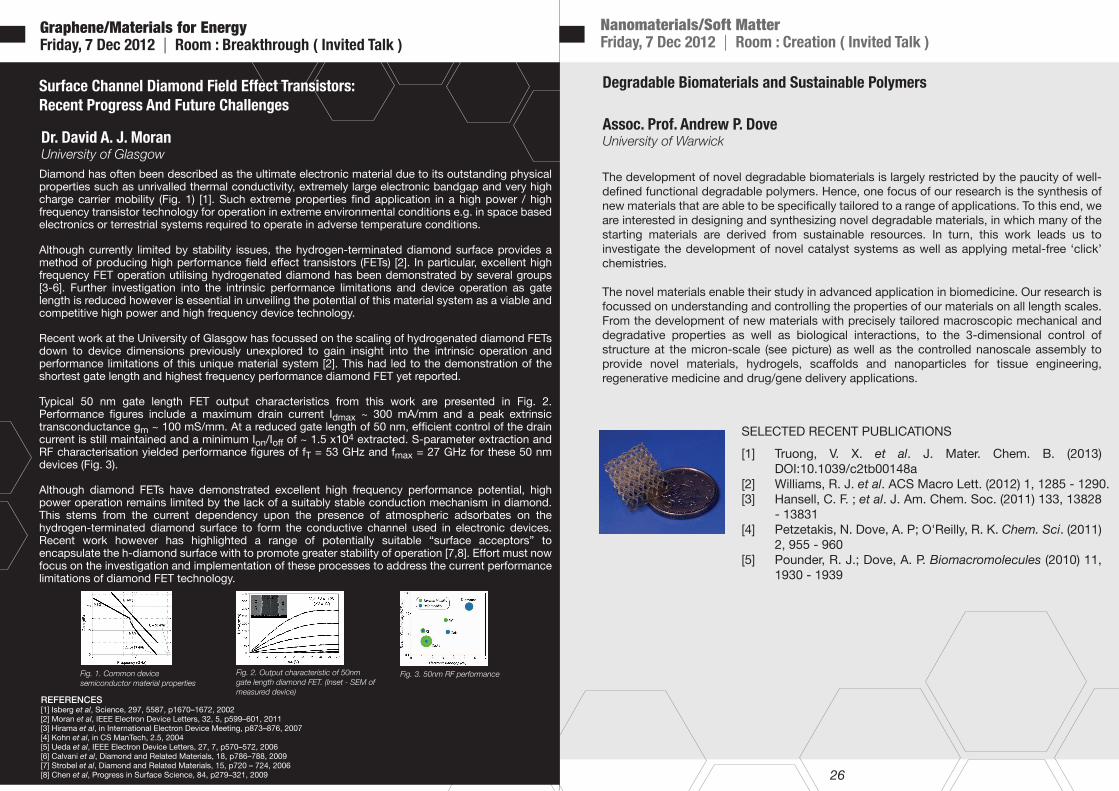
Dr. David A. J. Moran University of GlasgowDiamond has often been described as the ultimate electronic material due to its outstanding physical properties such as unrivalled thermal conductivity, extremely large electronic bandgap and very high charge carrier mobility (Fig. 1) [1]. Such extreme properties find application in a high power / high frequency transistor technology for operation in extreme environmental conditions e.g. in space based electronics or terrestrial systems required to operate in adverse temperature conditions.
Although currently limited by stability issues, the hydrogen-terminated diamond surface provides a method of producing high performance field effect transistors (FETs) [2]. In particular, excellent high frequency FET operation utilising hydrogenated diamond has been demonstrated by several groups [3-6]. Further investigation into the intrinsic performance limitations and device operation as gate length is reduced however is essential in unveiling the potential of this material system as a viable and competitive high power and high frequency device technology.
Recent work at the University of Glasgow has focussed on the scaling of hydrogenated diamond FETs down to device dimensions previously unexplored to gain insight into the intrinsic operation and performance limitations of this unique material system [2]. This had led to the demonstration of the shortest gate length and highest frequency performance diamond FET yet reported.
Typical 50 nm gate length FET output characteristics from this work are presented in Fig. 2. Performance figures include a maximum drain current Idmax ~ 300 mA/mm and a peak extrinsic transconductance gm ~ 100 mS/mm. At a reduced gate length of 50 nm, efficient control of the drain current is still maintained and a minimum Ion/Ioff of ~ 1.5 x10⁴ extracted. S-parameter extraction and RF characterisation yielded performance figures of fT = 53 GHz and fmax = 27 GHz for these 50 nm devices (Fig. 3).
Although diamond FETs have demonstrated excellent high frequency performance potential, high power operation remains limited by the lack of a suitably stable conduction mechanism in diamond. This stems from the current dependency upon the presence of atmospheric adsorbates on the hydrogen-terminated diamond surface to form the conductive channel used in electronic devices. Recent work however has highlighted a range of potentially suitable “surface acceptors” to encapsulate the h-diamond surface with to promote greater stability of operation [7,8]. Effort must now focus on the investigation and implementation of these processes to address the current performance limitations of diamond FET technology.
Fig. 1. Common device semiconductor material properties
Fig. 2. Output characteristic of 50nm gate length diamond FET. (Inset - SEM of measured device)
Fig. 3. 50nm RF performance
REFERENCES[1] Isberg et al, Science, 297, 5587, p1670–1672, 2002[2] Moran et al, IEEE Electron Device Letters, 32, 5, p599–601, 2011[3] Hirama et al, in International Electron Device Meeting, p873–876, 2007[4] Kohn et al, in CS ManTech, 2.5, 2004[5] Ueda et al, IEEE Electron Device Letters, 27, 7, p570–572, 2006[6] Calvani et al, Diamond and Related Materials, 18, p786–788, 2009[7] Strobel et al, Diamond and Related Materials, 15, p720 – 724, 2006[8] Chen et al, Progress in Surface Science, 84, p279–321, 2009 26
Controlled Growth And Applications Of Nanoscale Materials
“Reduced Graphene Oxide Conjugated Cu2O Nanowire Mesocrystals for High-Performance NO2 Gas Sensor” J. Am. Chem. Soc. 2012, 134, 4905-4917, Deng, S; Tjoa, V; Fan, HM; Tan, HR; Sayle, D. C.; Olivo, M.; M., Subodh; Wei, J.; Sow, CH“K-Enriched MoO3 Nanobundles: A Layered Structure with High Electric Conductivity” J. Phys. Chem. C, 2012, 116, 3962-3967, Hu, Z.; Zhou, C.; Zheng, M.; Lu, J.; Varghese, B.; Cheng, H.; Sow, CH“Optical and electrical applications of ZnSxSe1-x nanowires-network with uniform and controllable stoichiometry”, Nanoscale, 2012, 4, 976-981, Lu, J.; Liu, H.; Sun, C.; Zheng, M.; Nripan, M.; Chen, G.S.; Subodh, G. M.; Zhang, X.; Sow, CH“Facile One-Step Synthesis of CdS(x)Se(1-x) Nanobelts with Uniform and Controllable Stoichiometry”, J. Phys. Chem. C, 2011, 115, 19538-19545, J., Lu; C., Sun; M., Zheng; M., Nripan; H., Liu; GS, Chen; X., Zhang; M.G., Subodh; CH Sow“Photothermoelectric Effects in Localized Photocurrent of Individual VO(2) Nanowires” J. Phys. Chem. C, 2010, 114, 15149-15156, Varghese, B., Tamang, R., Tok, ES, M.G., Subodh G, Sow, CH“Structure-Mechanical Property of Individual Cobalt Oxide Nanowires”, Nano Lett. 2008, 8, 3226-3232, Varghese, B., Zhang, YS, Dai, L., Tan, V. B. C. Lim, CT, Sow, CH
[1]
[2]
[3]
[4]
[5]
[6]
Assoc. Prof. ChorngHaur SowNational University of Singapore
Nanoscale materials have attracted great interests in recent years. One- dimensional and two-dimensional nanostructures such as nanowires, nanorods, nanowalls, nanosheets, and nanojunctions or networks are an important category of nanostructured materials with great potential as important components for nanoscale devices with various interesting functions. Thus, in the past decade, many techniques have been developed for the synthesis of such nanostructured materials. Some examples of these techniques include chemical vapor deposition, vapor-liquid-solid growth, vapor-solid growth, oxide-assisted growth, carbothermal synthesis, hydrothermal growth and etc. With these methods, one can synthesize a wide variety of nanostructured materials including binary and ternary II-VI alloys, hierarchical metal oxide and etc. In addition to the above mentioned techniques, a wide variety of nanoscale metal oxide materials with fascinating morphologies can be synthesized by heating pure metallic foils or wires in appropriately controlled atmospheres. Many of these nanoscale material exhibits unique properties rendering them potentially attractive materials for possible applications. In this report, we will present our recent efforts in the growth and characterizations of these nanoscale materials with emphasis of the growth mechanism and potential applications of these nanoscale materials.
REFERENCES:
Bio-inspired nanomaterials for energy conversion
Graphene/Materials for EnergyFriday, 7 Dec 2012 | Room : Breakthrough ( Invited Talk )
Bio-inspired nanomaterials, inspired by the diverse and sophisticated materials and hierarchical material systems found in nature, are becoming of increasing interest. Currently, it more focuses on developing a fundamental understanding of the synthesis and hierarchical organization of natural occurring materials, and uses this understanding to engineer new eco-friendly "bio-inspired" materials for diverse applications. This talk will describe our recent efforts on developing bio-inspired nanomaterials for energy conversion. First, I will show several examples on how we developed universal approaches for creating bio-inspired hierarchical structures for energy storage. When the bio-inspired hierarchical structures were used as electrode materials, they behaved enhanced energy storage performance. Then, I will discuss how the bio-inspired materials can be developed and used for light harvesting with enhanced photo-activity. Finally, the examples on the bio-inspired hierarchical artificial photosynthetic systems for solar hydrogen evolution will be presented.
REFERENCES[1] Isberg et al, Science, 297, 5587, p1670–1672, 2002[2] Moran et al, IEEE Electron Device Letters, 32, 5, p599–601, 2011[3] Hirama et al, in International Electron Device Meeting, p873–876, 2007[4] Kohn et al, in CS ManTech, 2.5, 2004[5] Ueda et al, IEEE Electron Device Letters, 27, 7, p570–572, 2006[6] Calvani et al, Diamond and Related Materials, 18, p786–788, 2009[7] Strobel et al, Diamond and Related Materials, 15, p720 – 724, 2006[8] Chen et al, Progress in Surface Science, 84, p279–321, 2009
27 28
Graphene/Materials for EnergyFriday, 7 Dec 2012 | Room : Breakthrough ( Invited Talk )
Advanced Functional Fibres could be an exciting area researchers would like to work to develop new materials for tomorrow.For many decades, industries are using standard polymeric materials for commercial and military applications. Researchers are trying very hard to look for new materials for higher performance in term of mechanical strength and toughness.
To achieve this, one way is to develop new process on existing materials and the second option will be to development new material.
My paper will discuss on developing a new hybrid material using a new process. It is about exploring using existing materials couple with silkworm silk and or spider silk via a custom build multi-tip nanofibre electrospinning process.
Breakthroughs like discovery of wonder polymeric material and graphene do not always happen, and look into Natural silk-based materials from silkworms and especially spiders, because they are excellent candidates to give high mechanical strength and thermal conductivity.
With our current research, our researchers are able to enhance the strength of the silkworm silk by another 30% in strength and an additional of 50% more in elongation. With the right pre and post -processing of the material, there is a possibility we could functionalizing the product to deliver intrinsic and durable properties for materials of tomorrow.
In short, Advanced Functional Fibres could be functionalized and open the vast possibilities materials to achieve: antimicrobial, permanent colours, special smells that could be therapeutic, highly conductive for rapid cooling, and the list continues as technology advances.
Advanced Functional Fibres Computational Energy Materials Science: Recent Developments And ApplicationsDr. Gilberto TeobaldiUniversity of LiverpoolImplementation of a more sustainable energy economy relies on development of improved, industrially viable photocatalytic, photovoltaics, electrochemical energy conversion and storage devices. Atomic-scale understanding of the different materials and interfaces constituting such devices is crucial for the development of novel solutions. This, in turn, requires the possibility of accessing the atomic-scale parameters governing the thermodynamics and kinetics of atom, charge, energy transfer processes at the device interfaces. Along these lines, I will present an overview of recent results on:
(i) Scanning tunnelling microscopy contrast mechanisms for TiO2 [1]. Controlled dual mode Scanning Tunnelling Microscopy (STM) experiments and first-principle simulations show that the tunnelling conditions can significantly alter the positive-bias topographic contrast of geometrically corrugated titania surfaces such as rutile TiO2(011)-2x1. The mechanisms of contrast formation are elucidated in terms of the subtle balance between the surface geometry and the different vacuum decay lengths of the topmost Ti(3d) and O(2p) states probed by the STM-tip apex.
(ii) Density Functional Theory (DFT) investigation of the geometry and electronic structure of aluminosilicate and aluminogermanate nanotubes [2]. DFT simulations elucidate the previously reported polarisation of the nanotube walls as originating from a balance between compositional and geometrical factors. The peculiar electronic structure of the systems, leading to localisation of the low-energy conduction band and high-energy valence band edges on different sides of the tube cavity, is presented and discussed in terms of possible photo-catalytic applications.
(iii) Linear-scaling constrained Density Functional Theory in ONETEP [3a]. Very encouraging results have recently appeared regarding the potential of constrained Density Functional Theory (cDFT) for the study of charge (energy) transfer and chemical reactivity [3b]. Here we present the implementation of cDFT in the ONETEP program [3a]. The linear-scaling nature of the cDFT implementation opens up for cDFT simulation of systems up to a few thousands of atoms on academically available hardware. This should make the method useful for the study of extended interfaces present in photocatalysts, solar cells, fuel cells, and batteries.
29 30
Graphene/Materials for EnergyFriday, 7 Dec 2012 | Room : Breakthrough ( Invited Talk )
Nijhuis, C. A.; Reus, W. F.; Barber, J.; Dickey, M. D.; Whitesides, G. M. Nano Lett. 2010, 10, 3611.Nijhuis, C. A.; Reus, W. F.; Siegel, A. C.; Whitesides, G. M. J. Am. Chem. Soc. 2011, 133, 15397
[1][2]
Asst. Prof. Christian A. NijhuisNational University of Singapore
Understanding the mechanisms of charge transport across molecules, or self-assembled monolayers, is important in organic based photovoltaics, OLEDs, energy storage, bio-electronic devices, etc. Issues regarding how molecular orbitals couple to the electrodes, or the influences of subtle changes of the intermolecular interactions between the molecules in the SAMs, on the performance of molecular electronic devices have rarely experimentally been addressed.
We identified a molecular diode: junctions with SAMs of S(CH2)11Fc, i.e., SAMs with ferrocene at the top, on ultra-flat Ag bottom-electrodes contacted with EGaIn (an eutectic alloy of Ga and In) top-electrodes rectified currents with a rectification ratio of 100, while those junctions with SAMs of S(CH2)10CH3, i.e, SAMs without Fc units, did not rectify.¹,²
To study the influence of subtle changes in the intermolecular interactions between the molecules in the SAMs, and the coupling of the molecular orbitals with the electrodes, we fabricated devices with a series molecules of the type S(CH2)nFc (with n = 3, 4, ..., 15) and SCnFcCn-13 (with n = 1, 2, 3, ..., 15), respectively. We found that devices with n is odd are ten times better diodes than those devices with n = even. This so-called odd-even effect originates from small changes in the structures of the SAMs, which, in turn, depends on the interactions between the molecules in the SAM. By controlling the coupling of the molecular orbitals with the electrodes, we succeeded at “turning” around a diode at the molecular level. Thus, we are able to control the direction of rectification at the molecular level.
REFERENCES:
Organic-inorganic Hybrid Nanomaterials: Synthesis, Modification And Property InvestigationDr. Xiaoying QiSingapore Institute of Manufacturing Technology
In our work, we aim to develop organic-inorganic hybrid materials with emphasis on simplifying the synthetic methods, optimizing their structural control, enhancing their solubility and improving their physicochemical properties. Conjugated molecules with designed structural, chemical and physical properties were chosen as organic building blocks, and low dimensional inorganic materials including 0 D nanoparticles, 2 D nanosheets, graphene for instance, were selected as the inorganic components to synthesize novel hybrid materials with desired properties. These studies could provide useful fundamental guidelines and the material design concepts to the field of materials science and technology.