TIMING MODELS FOR MOS CIRCUITS BY Mark Alan Horowitz January 1984 Prepared under US Army Research Office Contract No. DRAG-29-80-K-0046 Integrated Circuits Laboratory Stanford Electronics Laboratories Stanford University, Stanford, California
Transcript
TIMING MODELS FOR MOS CIRCUITS
BY
Mark Alan Horowitz
January 1984
Prepared under
US Army Research Office
Contract No. DRAG-29-80-K-0046
Integrated Circuits Laboratory
Stanford Electronics Laboratories
Stanford University, Stanford, California
@ Copyright 1984
bYMark Alan Horowitz
-ii-
Abstract
Performance is an important aspect of integrated circuit design, and depends
in part on the speed of the underlying circuits. This thesis presents a new method
of analyzing MOS circuit delay, based on a single-time-constant approximation.
The timing models characterize the circuit by a single parameter, which depends
on the resistance and capacitance of the circuit elements. To ensure the single-
time-constant approximation is valid for a particular circuit, the timing models
provide both an estimate and bounds for the output waveform. For circuits where
the bounds are poor, an improved timing model is derived. These simple models
provide insight about circuit performance issues, as well as determining the circuit
delay.
The timing models are first developed for linear networks and then are extended
to model MOS circuits driven by a step input. By using the single-time-constant
approximation, the output waveform of a complex MOS circuit can be modelled by
the output of a circuit consisting of a single MOS transistor and a single capacitor.
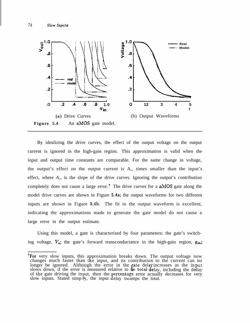
Finally, a new circuit model of a gate is used to derive the output waveform
of a circuit driven by an arbitrary input. The resulting timing model does not
depend strongly on the shape of the input: the output waveform only depends on
the input’s slope at the gate’s switching voltage.
Replacing a capacitor with a voltage source. . . . . . . . . . . . 109
Improved bounds for an RC tree with a pole-zero pair. . . . . . . 111
-X-
List of Symbols
a The rise time of the input normalized to the time constant of the gate; theinput takes arf to ramp from 0 to full scale.
ake
Pke
ck
A lower bound on vk/ve for two nodes in an RC tree.
An upper bound on vk/ve for two nodes in an RC tree.
The capacitance at node k in an RC tree. For two-tree circuits, a secondsubscript indicates which tree the capacitor is in: ckl is in tree 1.
CT Total capacitance of the output network of a logic gate.
e A node in an RC tree, usually an output node.
f(V) A transformation of variables that converts a nonlinear resistor into onethat is pseudo-linear.
Se
Sm
rDe minus the integral of U, (Ve for a linear network).
The forward transconductance of a logic gate evaluated at the gate’sswitching voltage.
k
he
A node in an RC tree, usually used as a summing index.
In an RC tree, the resistance from the root to the last node on the pathto both node e and node k. Thus, Rkk is simply the total resistance fromnode k to the root. In two-tree circuits, a second subscript indicates whichtree is being referenced.
R,(Rf) The effective resistance of a logic gate in the low-gain region for a rising(falling) transient.
td The time required for the output of a transistor cluster to reach theswitching poi.nt of the next gate after the gate’s input crosses its switchingvoltage.
t, The time when a logic gate enters the low-gain region of its drive curves.For bounds, a second subscript is used to indicate whether this time is anupper (u) or lower (1) bound.
T(t)
7ae
The output waveform for a single- time-constant nonlinear circuit.
A lower bound on the time constant of output e’s slow mode in a nonlinearcircuit.
An upper bound on the time constant of output e’s slow mode in a non-linear circuit.
-xi-
TDC
TMe
TRC
71
An estimate of the output’s time constant. A ’ superscript indicates thetime constant is for a two-tree circuit.
The time constant of a logic gate driven by a step input.
Time constant of the input waveform. For a ramp input, ri,, is the inverseslope; for an exponential input, it is the exponential’s time constant.
An estimate of the coefficient of the s2 term in node e’s frequency responsedivided by rp.
An upper bound on the lowest frequency time constant of any output in alinear network, and is equal to the sum of the open circuit time constants.A ’ indicates the time constant is for a two-tree circuit.A lower bound on the lowest frequency time constant of output e in alinear network. A A superscript indicates an improved bound; ’ indicatesthe time constant is for a two-tree circuit.An estimate of the time constant caused by the first resistor in a mixednonlinear circuit.
An estimate of the lowest two poles of node e’s frequency response.
An estimate of the lowest frequency zero of node e’s frequency response.
The voltage at node e, usually an output voltage of the tree.
An estimate of the voltage at node e.
The voltage at node k.
The switching voltage of a logic gate.
The transformed voltage at node e, f(Ve).
An estimate of the transformed voltage at node e.
-xii-
Acknowledgments
Without the help of many people, this thesis would not have been possible; even
with their help, there were times when I still had my doubts. First and foremost,
I would like to thank my parents and my friends Tom and Jeannie Blank, and
Barbara Lee for keeping me going even when I thought the situation was dismal.
This thesis has benefitted from many helpful discussions I have had during my
stay at Stanford. Tom Blank, Robert White, Paul Penfield, Chuck Seitz, Robert
Mathews, John Newkirk, and Robert Dutton deserve special mention for reading
drafts of this work and providing valuable feedback. I would like to thank John
Newkirk and Robert Mathews for asking me a question about MOS circuit delay
that eventually lead to the work presented in this thesis, and for their helpful
discussions throughout. I am also grateful for the opportunity to work with Paul
Penfield. He is still the only person I know who, after a 2 minute conversation, can
point out the mistakes in my arguments. Finally, I would like to thank my advisor,
Robert Dutton, who has patiently watched, supported, and guided me on my trek
to find a thesis topic, and then helped refine the material into its present form.
This work was supported in part by the AR0 under research contract DUG-
29-80-K-0046. The author’s support by an IBM Fellowship during the 1981-1982
school year is also gratefully acknowledged.
. . .-Xlll-
Chapter 1
INTRODUCTION
A million-transistor integrated circuit (IC) may sound impressive, but if it
cannot out-perform a thousand-transistor integrated circuit, what use is it? Perfor-
mance is an important aspect of an IC and depends on two factors: the chip’s
micro-architecture and the speed of the underlying circuits. To develop a successful
chip, the designers must consider both factors. The best micro-architecture can be
made ineffectual by slow circuits, and fast circuits are wasted in a poor architecture.
Integrated circuit designers have many tools at their disposal to help them
estimate the performance of a chip. At an architectural level, the tools determine
how many primitive operations (clock cycles) the IC requires to complete a desired
task. At a circuit level, the tools numerically estimate the delay through the inter-
nal gates. Unfortunately these circuit-level tools only can analyze small designs.
They cannot simulate the entire chip to determine the time needed to perform a
primitive operation at an architectural level. This thesis bridges the gap between
architectural tools and circuit tools by providing a conceptually and computation-
ally simple method of modelling the delay through Metal Oxide Semiconductor
(MOS) integrated circuits.
1.1 Delay Estimation
Determining a chip’s performance directly is difficult because it is a large,
nonlinear circuit; an IC can contain tens of thousands of signals and hundreds of
thousands of devices. However, the limited interactions in a digital system allow
the IC to be partitioned into many smaller subcircuits. The chip delay then can be
determined by estimating the delay through the subcircuits. Partitioning the circuit
2 Introduction
converts the chip performance estimation problem into many simpler subcircuit
problems.
Currently, designers use empirical models to estimate subcircuit delays. They
determine the delay’s dependence on the circuit parameters by numerically simulat-
ing many circuits and performing curve fitting on the results. The disadvantages
of this technique are lack of error control in the resulting models and difficulty in
relating the delay back to the circuit elements.
This thesis describes a single- time-constant approximation for generating sub-
circuit timing models. This approximation allows the output waveform to be charac-
terized by a simple sum of resistances and capacitances. The timing model is com-
putationally simple, making it attractive for large MOS circuits. More importantly,
the close relationship between device parameters and the timing model makes it
easier for, a designer to determine a component’s effect on the total delay. Thus,
the timing models not only estimate how fast a circuit will operate, when necessary
they also can help designers determine how to speed up the circuit.
Most subcircuit outputs can be approximated by single-time-constant estimates.
To ensure the validity of this approximation, bounds on the output waveform also
are derived. When the bounds are poor, the estimate is not a good model of the
output, and an improved estimate and bounds are derived by using a more complex
model of the output waveform. The use of bounds removes the biggest limitation
of simple timing models - the uncertainty in the overall accuracy.
1.2 Organization
The next chapter describes earlier work in delay modelling. To apply system-
analysis techniques to MOS integrated circuits, the chip must be partitioned into
transistor clusters, sub-circuits that can be viewed as digital logic blocks. From
transistor cluster delays, the chip delay can be easily determined.
1.2 Organization 3
Chapter 3 introduces a timing model for transistor clusters based on a linear
transistor model. By approximating transistors by linear resistors, transistor clus-
ters become linear RC trees. A timing model using the single-time-constant ap-
proximation, and following the derivation of Rubinstein, Penfield, and Horowitz
[RP83] yields an estimate and bounds on the output waveform. These models are
then extended to include systems without a single, dominant, time constant.
Chapter 4 removes the restriction that MOS transistors be modelled as linear
resistors. By looking at MOS transistors in a new way, the response of the nonlinear
network can be found using techniques analogous to the linear derivation. Again, a
single-time-constant model (both estimate and bounds) for MOS transistor clusters
is derived, which is similar, but not identical, to those for linear networks. The
similarity explains why the linear models work well; the differences show where
they will fail to be accurate. For circuits with multiple time constants, an improved
timing model is generated, again using the same basic technique as was used to
improve the linear models.
Chapter 5 describes the effect the input waveform has on the output of a
transistor cluster. When the input changes gradually with time, to determine
the output voltage requires modelling the output current of a logic gate versus
input and output voltages. The resulting model is quite simple and can be used
to show why certain gates are more sensitive to input slope than others. It leads
to improved timing models for transistor clusters. For fast input waveforms, these
models reduce to those derived in Chapter 3 and 4. For slow inputs, the delay
through the transistor cluster increases but it is only weakly coupled to the shape
of the input waveform. The input’s slope at the gate’s switching voltage is sufficient
to predict the output waveform.
Finally, Chapter 6 presents a synopsis of delay modelling and summarizes the
contributions of this thesis. Areas for further investigations are also described.
Chapter 2
DELAY ESTIMATION TECHNIQUES
Historically, tools for designing integrated circuit logic components have been
very different from the tools for constructing systems from these integrated circuits.
The design of a logic component is an analog design problem. Tools must model the
electrical elements used to determine the circuit’s digital characteristics: its delay,
noise margins, and power dissipation. On the other hand, in large system design,
the models of the underlying building blocks are digital. The system design tools
use a simplified model of logic components. The digital model hides the analog
aspects of the problem from the designer and the tools, allowing larger systems to
be designed.
As the complexity of integrated circuits increases, the line between component
and system design becomes increasingly fuzzy. Delay analysis tools for these com-
plex circuits must merge component-analysis techniques, to determine the subcircuit
delays, with system-analysis techniques, to compose subcircuit delays to yield the
chip delay.
2.1 Linear System Analysis
In the 1940s’ systems were neither digital nor integrated; they were multi-stage,
analog, tube amplifiers. Although design techniques for these analog amplifiers
might seem outdated compared to digital MOS VLSI design, the basis of the old
analog analysis techniques - the single-time-constant approximation - can be used
to generate MOS timing models.
6 Delay Estimation rechniques
Prior to the late 1960s’ performance estimation techniques were computation-
ally simple, since all calculations were done by hand. To simplify the analysis prob-
lem, all nonlinear elements were approximated by linear models. By looking at small
voltage excursions around an operating point (small-signal analysis), each nonlinear
element could be replaced by an effective linear element [GS69]. The response of this
linearized circuit was obtained using frequency-domain analysis, since the circuit’s
frequency response H(s), the Laplace transform of the system’s impulse response
h(t), could be determined directly from the circuit schematic [TA65].
The performance of an amplifier can be estimated from the low frequency
terms of H(s), since they dominate the output waveform. The single-time-constant
approximation models the response of the amplifier by a system with a single pole
[TA65]. In 1948, Elmore reported that, for a step input, the delay through a linear
amplifier was roughly equal to the first moment of its impulse response and that the
output rise time was approximately 6 times the second moment of the impulse
response minus the first moment squared [E148]. Based on the relationship between
the moments of h(t) and the derivatives of H(s), the delay and rise time can be found
from the frequency response. More sophisticated estimates for the output waveform
have subsequently been developed, including output bounds;+ however, the basic
approach, using the low frequency terms to estimate the output, has remained the
same.
Unfortunately, frequency domain analysis is valid only for linear networks.
When nonlinear elements are present, superposition, and therefore Laplace trans-
form techniques, do not apply. The growth of digital integrated circuits provided
both the impetus for nonlinear analysis techniques - the circuits are intrinsically
nonlinear - and an inexpensive method of performing the required computation
+A good review of this work is in [TA65], especially Chapter 8.
2.2 Circuit Simulation 7
- digital computers. Circuit simulation programs developed during the late 1960s
provided a method to estimate the performance of nonlinear circuits.
2.2 Circuit Simulation
A circuit simulation program computes output waveforms from a description
of the circuit and its input waveforms. Second-generation programs, like SPICE2
[Na75] and ASTAP-II [WJ73], have become an essential tool for integrated circuit
designers. The simulator makes finding circuit delays easy.+ The delay is simply
the amount of time between an input change and the corresponding change in the
simulated output voltage. For circuits with multiple inputs and outputs, the only
additional difficulty is choosing the input combination that gives the longest delay.
A circuit simulator uses numerical methods to solve the set of coupled nonlinear
differential equations that define the time dependence of the nodal voltages [CL75].
The program generates the equations by first using device models to relate device
currents to terminal voltages and then applying Kirchhoff’s current law to obtain
each capacitor current in terms’of the other device currents. The net result is a
set of equations relating the change in nodal voltages to the nodal voltages. Using
vector notation, this set of equations can be written as
where v is the vector of dependent nodal voltages - nodes not driven by a voltage
source.
Numerically integrating these equations provides an estimate of the output
waveform. Explicit integration methods are computational simple, but cannot be
+Assuming that the circuit and devices are modelled accurately, and that thesimulation converges [Pe82]. S imulators must solve a large set of coupled nonlinearequations to generate the initial dc solution. This task is very difficult, especiallyfor complex circuits.
3
8 Delay Estimation Techniques
used in a general program because they have poor numerical stability. Implicit
integration methods are more complex because finding the output voltages at each
time step requires solving a set of nonlinear algebraic equations:
Vn+l = Vn + f(vn+l)(L+l - tn), (2.2)
Circuit simulators solve Eq. (2.2) by using Newton’s method. The mth Newton-
Raphson interation involves finding the Jacobian of f(vz+r) and then solving the
resulting set of linear equations to generate vn”++l’, the new estimate. When the
difference between the new estimate and the old estimate is smaller than a set
tolerance, the simulator increments the time point and the process is repeated.
Since simulators use an implicit integration method, the maximum error in
the voltage estimates can be controlled by the user. Obtaining this error control,
however, requires evaluating every device model at each time step and then solving
a large set of nonlinear equations. As a result, circuit simulators work best with
relatively small circuits.
Macro-modelling is a technique developed in the mid 1970s to help simulators
analyze large circuits [RR78]. For MOS designs, the strategy was to reduce the
number of nodes required to represent a circuit by eliminating all nodes internal to
a logic gate [Ra73]. This simplification is possible because the internal dynamics
of a gate are normally not important. Although simulators could analyze larger
circuits using macro-models, simulation of the entire chip was still impossible.
To estimate the performance of MOS circuits too large for circuit simulators, a
faster technique, timing simulation, was developed. The programs MOTIS [CG75]
and MOTIS-C [FH77] are similar to circuit simulators in that they numerically
integrate nonlinear differential equations, but they use a simplified set of equations
and a simplified solution method to speed program execution. An undesirable effect
of these simplifications is an increase in the uncertainty of the result; the output
error can be bounded only for a limited class of circuits.
2.2 Circuit Simulation 9
Timing simulation is based on a gate-level, rather than a transistor-level,
description of the circuit. Gate macro-models lower the number of nodal voltages
which must be determined. To reduce program execution time further, timing
simulation only evaluates changing nodes. It updates gates with changing inputs;
gates with stable inputs are ignored. Since at any particular time, most of the nodes
have a stable voltage, i.e. are latent, only a small fraction of the circuit needs to
be evaluated at each time step. Exploiting circuit latency together with the other
simplifications make timing simulation about two orders of magnitude faster than
circuit simulation.
Recently there has been work on third generation circuit simulators [HS81,
LS82, SK83]. These programs are roughly the same speed as timing simulation, but
maintain the accuracy and error control of circuit simulation. Although these new
programs hold great promise as circuit analysis tools, they do not solve the delay
modelling problem. The new programs still suffer from two problems fundamental
to all numerical simulators: slow execution speed - the programs are still orders
of magnitude too slow to use to analyze an entire MOS IC - and an inability to
provide information on what causes the circuit delay.
Although a simulation program can determine the delay, it cannot diagnose
why the circuit is slower than expected or indicate how the delay can be reduced.
Solving the numerical equation yields the correct. answer but does not find the right
question. This information can be obtained only when the analysis tool understands
the circuits being evaluated. The result of this limitation is that experienced MOS
designers use SPICE to get a feel for the technology - to calibrate their internal
models - in addition to using it to analyze a particular circuit.
As the next section will show, for digital systems, the problem of estimating
the delay through a large circuit can be transformed into a problem of estimating
the delay through t,housands of subcircuits. However, this transformation only is
useful if a good subcircuit timing model exists.
10 Delay Estimation Techniques
2.3 System Timing Analysis
Even in the 196Os, digital systems were large and, as a result, complexity was
a major issue. The controlled interactions in such a system was used to limit the
complexity of simulation. Because these systems are constructed from digital circuit
blocks (logic gates) the analog nature of the circuits are hidden by the external
digital model. A simulator for logic need only model the delay and logical function
of each block.
The controlled interaction of digital gates also enables logic simulation pro-
grams to exploit circuit latency. Since a gate is unidirectional, its output can
change only if one of its inputs change. Evaluating only gates that have changing
inputs (selective trace), rather than all possible gates, greatly reduces the number
of evaluations at each time step.
Unfortunately, logic simulation only gives the delay for the input changes that
are tested. Unless all possible machine states are tested, there is no guarantee
that the longest delay found during logic simulation is the longest delay for the
system. To remove this limitation, value-independent timing analysis or timing
verification was developed in 1966 [KC66], bII was not applied to system designt
until the early 198Os, for example [McWSO, MoN]. This timing analysis uses only
the timing portion of the logic specification. Without the logical description, the
timing specification becomes a signal flow graph; signals flow into gates, experience
some delay, and then leave. The delay through any path from an input to an output
is simply the sum of the delays of the gates on that path. More important, the
worst-case delay through the logic can be determined by using a PERT scheduling
algorithm, whose time complexity is linear in the number of gates.
In the early 1970s IC designers began putting large systems onto a single MOS
chip. Since these circuits were too complex for circuit simulation tools, the designers
turned to logic simulation and timing analysis to estimate the circuit delay. Before
2.4 MOS G a t e Delay Models 11
these tools could be applied to MOS designs, two questions needed to be answered:
what are the ,logic blocks for MOS circuits, and what are the delays through these
logic blocks? When systems were built from bipolar SSI and MS1 integrated circuits,
the answers to these questions were obvious; the logic blocks were the ICs, and the
delays were published as part of the IC specification. For large integrated circuits,
the answers were no longer as clear.
2.4 MOS Gate Delay Models
The digital model is an abstraction that suppresses the analog nature of the
input and output waveforms, and represents the circuit by a boolean function.
Another constraint of digital circuits is unidirectionality: a block’s input is not
affected by its output. Both logic simulation and timing analysis use this constraint
when they assume changes only propagate from the inputs of a block to its output.
A logic block is any subcircuit that can be accurately represented by a digital
model. In MOS circuits, MOS transistors provide unidirectional coupling. The
transistor’s gate voltage affects its source and drain voltages, but the reverse cou-
pling is small and can be ignored. t The MOS transistors also provide gain, so the
details of their gate voltages has a minor affect on their outputs. Thus a MOS logic
block is a subcircuit whose inputs and outputs are all connected to the gates of
MOS transistors. Logic blocks that cannot be subdivided into smaller logic blocks
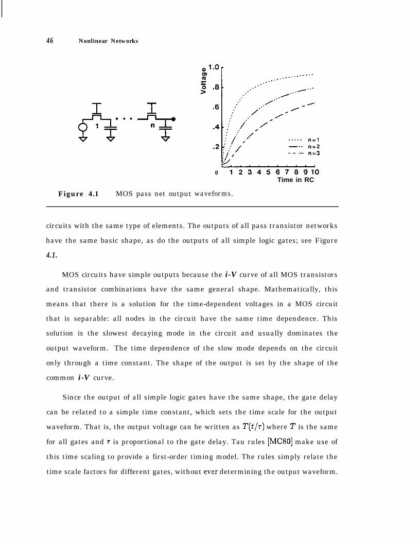
are referred to as transistor clusters; see Figure 2.1.
A transistor cluster can be viewed as an MOS logic gate and its associated out-
put network. The output network includes any pass transistor network connected
to the gate’s output as well as the the parasitic resistance and capacitance of the
tThe reverse coupling is capacitive coupling between the source and drain and thegate. For most timing questions this coupling is small enough that it can beignored; an effective grounded capacitor can be used instead.
12 Delay Estimation Techniques
Output Network
Pass Transistor
Transistor ClusterFigure 2.1 An nMOS transistor cluster
output wires. Both the gate and output network can be quite complex. The gate
can be a large AND-OR-Invert structure and the output network can include a
large pass network, or a complex wire tree. Wire parasitics, especially the wire
capacitance, are an important component of the transistor cluster, and must be in-
cluded for an accurate timing model. Fortunately, programs are available to extract
parasitic capacitance [SA78] and resistance [HD83] from a layout description.
Initial attempts to create delay models for transistor clusters used circuit
simulators to generate empirical timing models. Such empirical models limit the
kinds of transistor clusters that can be modelled - a simple gate with a capacitor
load is typical [PS72]. Although recent timing models can accommodate more
complex transistor clusters [AD82, OM83], the models are still very limited.
These empirical MOS timing models are more complex than the bipolar gate
models. In addition to having different rise and fall delays, the delay through a
MOS transistor cluster depends on the slope of the input waveform. For accurate
2.4 MOS Gate Delay Models 13
timing analysis, this dependence means the shape of the signal during the transition
is important; the timing models must determine both the delay and the slope of the
output waveform.
In 1981, Penfield and Rubinstein presented a technique to bound the output
waveform of a linear RC tree, based on a single-time-constant approximation [PR81].
This method can be applied to generate delay models for MOS transistor clusters
by making two approximations: (1) modelling the input of the clusters by step
waveforms, and (2) modelling conducting transistors by linear resistors. This tech-
nique has two advantages over empirical models. First, it can be applied to any
type of transistor cluster, so a separate model for each type of cluster is no longer
needed. In addition, it can relate the delay back to the circuit, showing which
portions need improvement. As a result of its generality, this model was quickly
incorporated into many MOS timing-analysis programs, for example, TV [Jo831 and
Auto-Delay[Pu82].
The linear RC tree model has many limitations. Since transistors are not linear
devices, their effective resistance values must be determined empirically. Although
the timing model produces bounds, these waveforms only bound the output of
the ideal linear model, not the output of the nonlinear circuit. The relationship
between the model and the actual MOS circuit remains unchecked. The error in
the estimated delay can be large even when the bounds are good because of the
approximations used to derive the linear circuit model. Since the model provides no
method to estimate or bound its error, the accuracy of results cannot be quantified.
This thesis generalizes the concepts used in finding bounds for RC trees - using
the single-time-constant approximation - to generate improved timing models for
MOS transistor clusters. In particular, the new models remove the need to model
transistors as linear resistors and inputs as step waveforms. Thus, the waveform
bounds of the new model provide a valid accuracy check on the timing estimate.
14 Delay Estimation Techniques
The next chapter begins by describing linear timing models for transistor clusters,
since they form the foundation of the more advanced timing models.
2.5 Summary
The complexity of current MOS integrated circuits makes it infeasible to es-
timate a chip’s delay directly using a circuit simulator. A chip contains too many
nodes, even considering circuit latency, to numerically solve for the voltage at each
node. Instead, the circuit must be viewed as a large digital system. The delay can
then be estimated from the delays of its transistor clusters, the logic blocks for
MOS circuits. Currently, designers use simple empirical timing models to estimate
a transistor cluster’s delay. The uncertainty resulting from the inaccuracy of the
models is the main limitation of this technique.
Chapter 3
LINEAR NETWORKS
3.1 Overview
This chapter derives timing models for linear networks. To apply these models
to a transistor cluster, MOS transistors must be approximated by linear resistors.
Although this is a crude approximation, the resulting model provides a first-order
estimate to the cluster’s output waveform. The advantage of this linear approxima-
tion is that linear network theory can be used to help derive the timing models. The
insight gained from the linear derivation is used in later chapters to derive more
accurate timing models.
When MOS transistors are approximated by linear resistors, a transistor cluster
becomes a linear RC tree. Because the model is linear, a qualitative description of
the output waveforms can be found using frequency domain analysis. The insight
gained from this analysis will guide the development of a more formal timing model.
The derivation follows that of Rubinstein et al. t The resulting model uses three
easily computed time constants to produce an estimate of and bounds on the output
waveform of a linear RC tree. Estimating the output waveform avoids the difficult
question of defining the delay for a system with slow rise and fall times. From the
output estimate, the approximate time required for the voltage to reach any level
can be determined.
tPenfield and Rubinstein [PRSl] developed the initial method for bounding the delayin RC trees. After reading their work, this author developed a simpler derivation,which yielded slightly better bounds. This improved derivation is presented in[RP83] and is used in this chapter.
16 Linear Networks
The bounds serve to check the single-time-constant approximation used to
generate the estimate. For some outputs, the estimate matches the real output,
yet the bounds are poor. The bounds for these circuits can be improved by simply
improving ran, one of the time constants used to generate the bounds. For other
outputs, both the estimate and bounds poorly match the real output, because the
real output does not have a single dominant time constant. To better represent
these outputs, a two-time-constant estimate is derived.
Finally, the timing models are extended to estimate the output of an RC tree
driven’by another RC tree. This situation occurs in MOS circuits when a pass
transistor turns on, connecting a new network to the output of a previously settled
gate. The extension also provides a method to estimate the output of a logic gate
whose internal capacitance is not negligible.
3.2 Modelling Transistor Clusters
A transistor cluster represents a logic gate and its associated output net; see
Figure 3.1. Although all the outputs of this cluster are logically equivalent, the
voltages at the outputs need not be the same because of the resistance of the output
net. Hence, a unique delay is needed for each physical output of the cluster. Both
the gate and the output net must be characterized to generate a timing model for
this structure. Two approximations simplify this task: the inputs to the cluster are
modelled as step waveforms and conducting MOS transistors are modelled as linear
resistors.
Transistors have only two possible states, if step inputs are assumed: fully
conducting and not conducting. A transistor can be modelled as a non-linear resistor
in series with a switch. The transistor’s gate voltage controls the state of the switch.
Using this model of a transistor, a resistor connected to ground models the logic gate
for a low output; a resistor connected to the power supply models a high output.
Cluster
3.2 Modelling Transistor Clusters 17
Model
Figure 3.1 A nMOS transistor cluster.
The value of the resistor is equal to the resistance through the pullup transistor(s)
in the high state and is equal to the resistance through the pulldown transistor(s) in
the low state. In nMOS, the pullup transistor is ignored in the low state since the
resistance of the pulldown transistors is much less than the resistance of the pullup
transistors. When the gate’s output changes, the resistive path in the gate drives
the output net, changing all the output capacitors from the old output value to the
new value.
By using a linear resistor to model a conducting transistor, the circuit model
of a transistor cluster becomes a linear RC tree: a network of floating resistors
(possibly distributed RC lines) and grounded capacitors driven by a voltage source,
where a unique resistive path exists from each capacitor to the voltage source.+
Figure 3.2 shows an RC tree model of a transistor cluster. The node connected to
the voltage source is called the root of the tree.
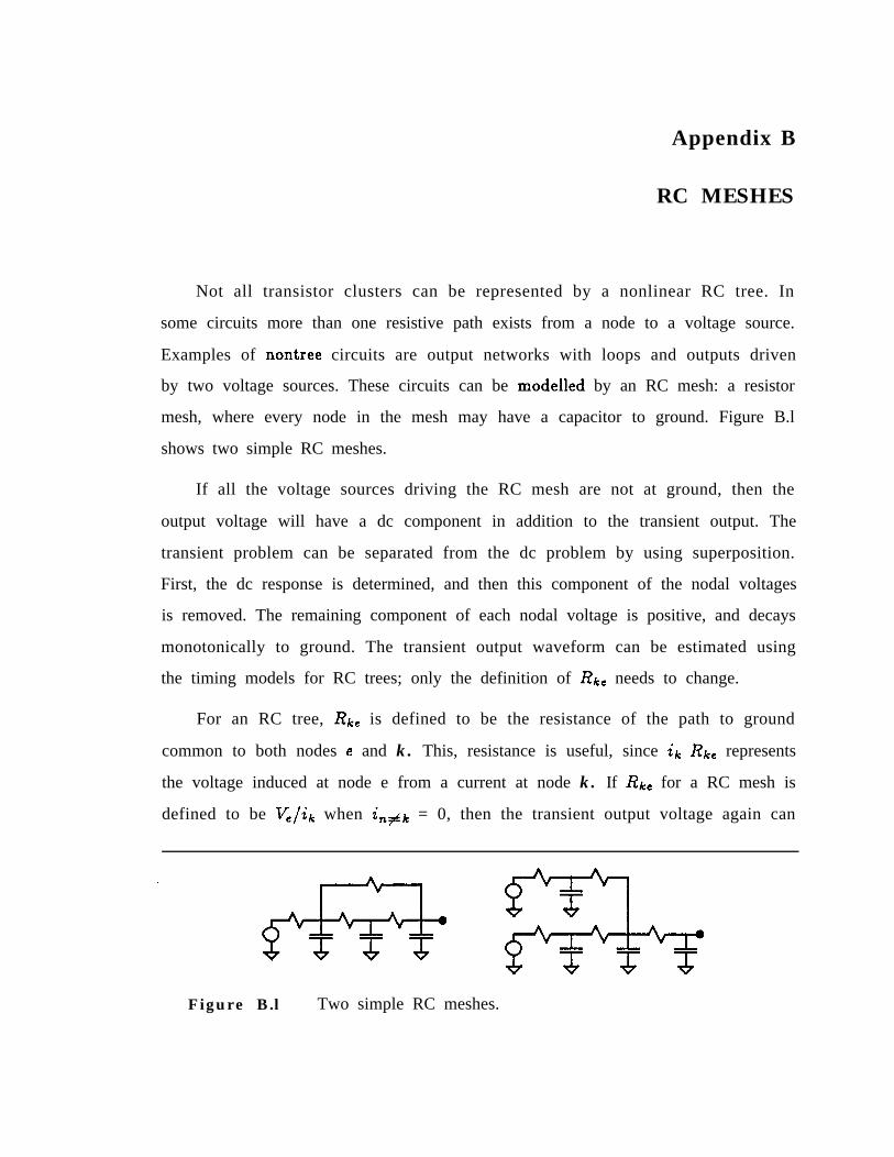
t This assumes there is a unique signal path from each capacitor in the output netto the gate’s output. Althoucircuits are unusual. Rarely f
h it is possible to have output nets with loops, theseoes a signal net split off only to recombine with itself.
In the situation where loops areP
resent, the model of a transistor cluster becomesan RC mesh: The timing mode s for these structures are very similar to modelsfor RC trees; see Appendix 13.
18 Linear Networks
Root
\ R1
Figure 3.2 An RC tree.
The voltage source and the first resistor (R 1 model the logic gate; the rest of)
the RC tree models the output network. When the logic gate changes state (because
its inputs change), both the value of the voltage source and the first resistor (RI)
change. During a falling transition, the output of the voltage source is ground and
the first resistor is equal to the resistance through the pulldown transistor; during
a rising transition, the output of the voltage source is Vpowcr and the first resistor
is equal to the resistance through the pullup transistor. For determining the delay,
the output network is assumed to have settled to the previous state before the new
change occurs: output changes do not interact. Using this assumption, the output
of a transistor cluster is equal to the output of an RC tree driven by a step voltage
source. This assumption is quite good for digital circuits, but breaks down for
circuits that use positive feedback in an attempt to improve circuit performance.
This limitation is discussed further in Chapter 6.
3.3 Qualitative Analysis
Using the linear transistor model: a MOS logic gate driving a capacitor load
is represented by a single-resistor, single-capacitor circuit; its output is a simple
exponential. Surprisingly, the output of most complex transistor clusters can be
r
3.3 Qualitative Analysis 19
accurately approximated by an exponential waveform. To understand why the
outputs are so simple requires looking at the frequency response of RC trees.
If an output can be well modelled by a single-resistor, single-capacitor circuit,
then its frequency response must be dominated by a single pole. A dominant pole
occurs when one pole is located at a much lower frequency than all the other poles
and zeros.+ In general, the output at the end of a series of identical elements has
a single pole response. For example, the voltage at the end of a long polysilicon
wire (modelled as a series of small RC sections) has a large number of poles, but is
nicely approximated by an exponential; see Figure 3.3. The high frequency poles
are most important during the initial transient, and here the approximation has its
largest error. But even at its worst, the error is still small. Using a linear transistor
model, the voltage at the end of a series of identical pass transistors resembles the
output of an RC line and also can be approximated by an exponential. Adding a
capacitive load at the end of an RC line (to model input or wire capacitance) lowers
the frequency of the dominant pole, which means the single-pole estimate is an even
better approximation to the real output.
There are two classes of linear networks that do not have a single-pole response.
Circuits with coincident poles may have a group of low-frequency poles that dominate
the output; circuits with a low-frequency pole-zero pair have a low-frequency zero
that partially cancels the dominant pole, causing the output to have a two-time-
constant behavior. Although these types of linear networks are easy to construct,
they rarely arise as a model for a transistor cluster.
tTo understand why higher frequency poles are less important, consider a ste,ptraversing a series of filters. Each filter corresponds to afrequency response. If the lowest frequency pole is put first, t
ole of the output sK en it will attenuate
the input’s hi h fre uency components.effect, as all tie big\
Subsequent poles will have only a smallfre uency components have alread been attenuated. The
larger the difference in po e frequencies the smaller the e7
Hhave on the output.
ect high frequency poles
20 Linear Networks
I 4.O .2 .4 .6 .8 1.0
Time in RC
Figure 3.3 Output of a uniform RC line.
- -. - Estimate- Real
I0 1 2 3 4 5 6
Time in RC
Figure 3.4 Output waveform of a circuit with three coincident poles.
Figure 3.4 shows a network with three closely spaced poles and its response.
The large range in resistance and capacitance required to generate coincident poles
means this type of circuit rarely occurs in MOS designs. The one exception is
in modelling busses. Here the bus driver and the bus capacitance form the low
impedance RC section, and the read circuitry form the high impedance section. If
the time constants of the two sections are roughly equal, then the circuit will have
two coincident poles.
Q, 1.0EYZ>o .8
.6
.4
.2
0
3.3 Qualitative Analysis 21
_ - - Estimate- Real
- I5 20 25 30Time in RC
Figure 3.5pair.
Output waveform of a circuit with a low-frequency pole-zero
An example of a network with a low-frequency pole-zero pair and its output
waveform are shown in Figure 3.5. The presence of a low-frequency zero partially
cancels the dominant polej causing the output waveform to have a slowly decaying
tail. Physically this type of output occurs when the dominate time constant in the
circuit is caused by capacitance that is located on a side branch of the tree and
not directly on the path from the root to the output. The voltage at the output
initially decays quickly with a time constant caused by the local output capacitance,
but eventually the voltage on the distant capacitance controls the output through a
voltage divider. This type of circuit also is rare as a transistor cluster model because
it requires one output of a gate to be much slower than another output of the same
gate. Usually a designer creates a circuit so all the outputs have roughly the same
timing. The one exception to this rule is in regular structures, where control wires
run in polysilicon and drive many circuits. The output closest to the control driver
will be much faster than the output at the end of the poly line and will have a
slowly decaying tail. But this fast output is usually not on the critical path. The
output of interest is normally the slowest one, the one at the end of the poly wire,
which has a single-pole response.
22 Linear Networks
3.4 Single-Time-Constant Model
The following derivation provides an approximate solution and bounds for each
output in a linear RC tree. Voltages have been normalized to range between 0 and
1. Att = 0 the logic inputs change causing the output net to change from a one
to a zero. For t < 0, all the nodes in the tree are 1 and at t = 0, the root of the
tree is grounded. The derivation for the rising waveform is similar. Nodal voltages
V, simply are replaced by 1 - V,.
The voltage at an output node e, V,, is equal to the voltage drop through the
resistors between e and ground - the root of the tree. This voltage can be found
by replacing each capacitor by its equivalent current source, i, = -C,dV,/dt, and
then using superposition. The output voltage is the sum of the contributions from
each individual current source. The voltage at node e caused by a current at node
I\: is just the current times the resistance of the path to ground (the driven input)
shared by the two nodes. Defining this resistance to be Rke,t the voltage drop
caused by current ik becomes Rke ik = -RkeCk s. Summing over all capacitor
currents in the tree gives the output voltage:
v, = - c dVkRkeck -k dt ’ (34
3.4.1 Waveform Estimate
Equation (3.1) is difficult to solve exactly because it involves a set of coupled
differential equations. The capacitors in the tree lead to many time constants.
Since most output waveforms are dominated by a single pole, a single-time-constant
estimate, V:, is used to model output voltage at node e. Replacing dVj/dt by
tFor example, R,,Ras =
is the total resistance from node n to ground. In Figure 3.2,RI and R34 = RI + R3.
3.4 Single-Time-Constant Model 23
akdV,/dt, where ak is an arbitrary constant, converts Eq. (3.1) into a single-time-
constant equation. The value of ak that gives the best estimate is 1, since this value
makes the integral of the error, s(Ve -V:) = xk R&k s(g - $$), zero Since vk
and V, have the same starting and ending points. The estimated output waveform
is a simple decaying exponential with a time constant rDe:
v:(t) = exP(+D& TDe = c R&k.k
The time constant, r&, is equal to the first moment of the circuit’s impulse response,
a quantity used to approximate the delay through linear amplifiers [E148]. The
output estimates shown in Figures 3.3-3.5 were generated using this model.
In the frequency domain, the single-time-constant estimate is equivalent to
modelling the output using a single-pole transfer function. The value of rDe matches
the frequency response of the output and the estimate at low frequencies: to first-
order terms in s.
3.4.2 Waveform Bounds
As we saw earlier, most transistor cluster outputs can be approximated by
a single-time-constant estimate. Unfortunately, there are also outputs where this
estimate is poor. To make the estimate more useful, waveform bounds are derived
to provide error control. If the bounds are close to the estimate, then the maximum
possible timing error is small: the real output is roughly exponential in shape. If the
bounds are very different from the estimate, then a more complex model is required.
To bound the voltage at output e requires a bound on Eq. (3.1). There is no
simple way to bound dl’k/dt, but it is possible to bound vk in terms of V’. Hence,
integrating Eq. (3.1) y Idie s an equation for the integral of V,, which can be bounded.
The bounds on the integral of V, then can be used to bound V,.
24 Linear Networks
Integrating Eq. (3.1) yields
/
t
V,(T)dr = c&C/c(l - Vi(t)).0 k
Defining se(t) to be r& - s Vet simplifies the above equation:
ge = c RkeCkVk-k
(3.2)
Bounding vk in terms of V, provides a method to bound Eq. (3.2). Since all voltages
in an RC tree decrease monotonically with time, the follow bounds on vk hold:t
Rke Rkkj+. 5 vk 5 -v,.ce he
Substituting the bounds into Eq. (3.2) bounds gc in terms of V,:
where
v, he= --;dt
rp = c RkkCk; *Re = cR2,,Ck
k k Ree ’
Bounding vk in terms of V, causes the bounds on ge to become single-time-
constant equations. The time constant of the lower bound is r&; the time constant
of the upper bound is rp. Both bounds on ge are equal to r& at t = 0, and decay
to zero. Using the ge bounds in Eq. (3.4) provides bounds on the output voltage,
V,:
9 < Se I TPKl=iower - * E eXP(-+Re) 5 K(t);
(3.5)Se > ge 2 ‘-ReVaupper - * 2 exp(---t/v) 2 K ( t ) .
tSince voltages have been normalized, s V has the dimensions of time
SFor a complete derivation see Appendix A.
3.4 Single-Time-Constant Model 25
The bounds only depend on three time constants, r&, Q,, and rp. TR, is a
lower bound on the output’s time constant; rp is an upper bound. When all three
time constants are similar in value, the estimate’s maximum error is small. The
error increases as the difference in the time constants increase.
The bounds on the output voltage in equation (3.5) can be improved by using
the additional constraints that V, decreases monotonically with time and V, < 1.
Using the monotonicity of V, gives
ge(t) + (t -.W(t) 5 ge(t’).
Replacing se(t) and ge(t’) with bounds, TR~V~ and r& exp(--t/rp) respectively, leads
to the following improved upper bound on the output voltage:
( l, 0 5 t 2 TDe --Re;
I TDC
t+&TDe -
VeP> ITRe 5 t 5 TP - TRe;
(3.6)
7D.Z -t + TP - TRe- exp ) TP - TRe 2 t.TP TP
since ge is TD, - s V,, using the constraint V,
on ge, which leads to a better lower bound on V,:
-t + TDe - TRe>
TRe
5 1 gives a better lower bound
t 5 TDe --Re;
t 2 TDe -rRe.
(3.7)
Although these new bounds are tighter than the previous ones (Eq. (3.5)), the
general dependence on the time constants remains the same. The difference between
TRe and rp controls the uncertainty in the estimate. The bounds for a circuit
with a low-frequency pole-zero pair are widely separated (see Figure 3.6), warning
26 Linear Networks
i1.0
z .8
.6
0
- - Upper Bound. . . _. Lower Bound- Real
-.__ -., .)___ . 45 10 1 5 2 0 25 30
Time in RC
Figure 3.6 Output bounds for a circuit with a low-frequency pole-zeropair. To, = 9, rRe = 5, rp = 29
.6
- - Upper Bound-. -. . Lower Bound
\ - Real
- - Upper Bound-. -. . Lower Bound- Real
.O .2 .4 .6 .8 1.0Time in RC
Figure 3.7 Output bounds for a distributed RC line. roe = .5, TRe =.33, rp = .5
the designer that the estimate is poor. For an output with a single-time-constant
behavior, the bounds are close to the estimate, as can be seen in Figure 3.7.
3.4.3 Computational Requirements
For the waveform estimate and bounds, three time constants characterize the
OUtpUt: rDe, r’Re, and 7~. These time constants are needed for each physical output
3.4 Single-Time-Constant Model 27
of a transistor cluster, since the outputs can have different waveforms. Each time
constant is a sum over all the capacitors in the network (for distributed elements
these sums become integrals), so for a network of n capacitors a time constant takes
O(n) time to compute. Repeating this process for all outputs requires O(n2) time,
assuming the number of outputs is proportional to the number of nodes (capacitors).
The time complexity can be reduced to O(n) by using an algorithm that finds
the time constants for all the outputs simultaneously. This reduction is possible
because the time constants for different outputs share common terms; finding the
time constants for the outermost nodes provides the inner time constants with little
extra computational effort. An algorithm for finding rDe for all nodes in a tree is
given in Figure 3.8. The algorithm for rR, is analogous.
3.4.4 Time Constant Interpretation
In addition to providing output bounds, rRe and rp provide useful information
about the network, especially for cases where the bounds are poor. For an output
dominated by a cluster of n poles all at the same frequency, r& is equal to rD,/n,
while rp remains approximately equal to r&. When low-frequency pole-zero pairs
are present, rp is much larger than r& without affecting r&. When rRe and rp are
both close to r&, the output is dominated by a single pole.
A small rRe does not imply coincident poles. A single pole dominates the
output of the RC tree shown in Figure 3.9, yet rRe is much less than rDe. This type
of circuit often occurs in modelling a bus. The bus capacitance (Cl) dominates
the circuit, but is located between the driving gate (RI) and the pass transistor
reading the bus (Rz). The particular voltage bounds used to generate r&, (Eq.
(3.3)) substantially underestimate the actual voltages present for this circuit. As
will be shown in the next section, improving the internal voltage bounds leads to
better single-time-constant bounds on the output waveform.
28 Linear Networks
n o e kl *e*R*F $ y-T C☯k l T
procedure findCT( k:node );(* cT[ k ] is the total cap. of the subtree with node k as its root. *)
begin@Fkl := C[ k 1;for all children i do begin
find&( i );CT[kl :=CT[k]+CT[i];
end;end;
procedure findrD(k:node);begin
for all children i do beginrD[i] :=rD[k]+R[findrD( i );
end;end;
i] cT[ i I;
beginTD[rOOt] := 0;find&(root);findrD(root);
end;
Figure 3.8 Algorithm to find rDe in linear time.
The bounds are poor for outputs where 7~ >> rD, because a single pole does not
dominate the output waveform. An exponential is a crude model of an output with
a slowly decaying tail. The upper bound over-estimates the output during the initial
fast decay, since the output is modelled by a waveform that decays at the slow tail
rate. The lower bound is also poor since it ignores the fast transient completely.
It becomes a lower bound on the slow tail, which is a valid, but not useful, lower
3.4 Single-Time-Constant Model 29
- - UpperBound\ - -. . - Lower Bound
\ - - - E s t i m a t e\- Real
\
.6 -
...4 -
.2 -*.
--_, -...L 1
0 50 100 150 200Time in RC
Figure 3.9 Circuit with a poor rRe. rDe = 110, TRe = 20, rp = 110.
bound on the actual output. To improve this output estimate a two-time-constant
model is needed.
3.4.5 Improved rRe
For an RC tree with a poor TR,, a capacitor (or group of capacitors) in the
middle of the network sets the circuit’s dominant pole. All voltages further from
the source, including the output node e, track this capacitor’s voltage. Yet the
lower bound on the dominant capacitor’s voltage is 2Ve instead of V, - A.
Approximating a node’s voltage by this lower bound causes the output bound to be
poor if Rke for the dominant capacitor is much less than I?,,. For the circuit shown
in Figure 3.9, the capacitor at node 1 dominates the circuit; the output tracks this
voltage. Yet, the lower bound on node 1 is &/lo, a poor approximation to the
actual voltage.
An improved bound on the output requires a better lower bound for v,. The
lower bound on vk in Eq. (3.3) is the lowest voltage possible given V, and positive
capacitor currents; t,he bound does not use any information about the time behavior
of the network. For an RC line, using this information leads to an improved voltage
30 Linear Networks
.6
.4
.2
I 80 50 100 150 200
Time in RC
Figure 3.10 Improved output bounds using +Re. roe = 110, fiRe = 101,TP = 110.
bound, which in turn improves rRe. t The improved time constant, ?Re, is
‘jRe = c akeRkeCk;he
ake = m a x -) l- rDe-rDk ’k Ree TRk >
Figure 3.10 shows the improved bounds for the RC line given in Figure 3.9.
The new r& greatly improves the bounds when the dominant capacitor lies on the
path from the output to driving gate. Outputs where +Re is still much smaller than
rDe have coincident poles and can be better approximated by a two-time-constant
estimate.
3.5 Two-Time-Constant Model
For outputs with multiple time constants, the problem with the single-time-
constant model is the assumption that all voltages in the network are proportional to
the output voltage. These networks have a low frequency pole caused by capacitors
tThe improved bounds are derived using the constraint -$$/Vn > --%/VP whennode q is downstream of n. For a more complete derivation of theimproved boundssee Appendix A.
3.5 Two-Time-Constant Model 31
off the path from the root to the output. As a result, the voltage on some nodes in
the circuit are not tightly coupled to the output voltage. To improve the estimate
and bounds for these outputs, the loosely coupled nodes are handled separately
from the other nodes. The resulting timing model has two time constants. Outputs
in this class are characterized by rp >> rDe.
3.5.1 Waveform Estimate
The improved estimate has two time constants - one to model the decay of
the initial transient and the other to model the slow decay of the output tail. The
improved estimate is the best two-pole, single-zero model of the output waveform.
This is the simplest system that can have a slow tail in its output response.
The second order estimate has three parameters: the time constants of the two
poles and the one zero. These time constants can be related to three characteristic
time constants of the output: the sum of the open circuit time constants, rp; the
first moment of the impulse response, r1),; and the second moment of the impulse
response, 2Tp(7De - 7~~). Setting the model’s characteristic time constants equal
to the characteristic time constants of the output yields the best estimate of the
output waveform. This choice of time constants matches the frequency response of
the output with the frequency response of the estimate at low frequencies. Unlike
the single-time-constant estimate, this model matches the output to second-order
terms in 9.
The model network transfer function can be written as
Hm(s) = (1+ slr;;(Z 4’ (3.8)
The characteristic time constants for this system are:
+The nthorder moment of the impulse resderivative of the transfer function evaluateB
onse is equal to -1” times the nthat s = 0.
32 Linear Networks
(3.9)Tp = 71 + 72,7172
TDe = rp - rl, ?-MC = -71 + 72
The first two time constants for the output are already known:
rp = c RkkCk, TDe = c RkeCk*k k
rMe can be found by generating the second order moment of the impulse response,
which is twice the first moment of the output voltage. Integrating by parts gives
- TMe)
or
Inverting the relations in Eq. (3.9) gives 71 and 72 in terms of the physical time
constants:72 = rp - TDe;
72,Tl = F(l f & - 47Me/7p).
The inverse Laplace transform of Eq. (3.8) gives the estimated output voltage:
v: =(7= - 71)e-t/z1 + (72 - 7,)emtirs .
T2 - 71(3.10)
This equation provides an improved estimate for all outputs, even those where
TP = TDe. The improved estimate is only slightly more complex than the single-
time-constant estimate, and requires two additional time constants, though rp is
needed for the bounds already.
Figure 3.11 shows the single-time-constant estimate, the second-order estimate,
and the actual output for the networks shown in Figures 3.4 and 3.5. The improved
estimate accurately reflects the actual output. The advantage of the two-time-
constant estimate is its ability to model the different decay rates of the output. The
estimate has the largest error when an output has many time constants, not just
3.5 Two-Time-Constant Model 33
.O 1 2 3 4 5 6Time in RC
(4
.6
.4
.2
- - - Estimate- - - 2nd Order Est.- Real
0 5 10 15 20 25 30Time in RC
(b)Figure 3.11 Two-time-constant Estimate for (a) the circuit with three
ccincident poles shown in Figure 3.4 - TD, = 3, rp = 3, TM~ = 1; andfor (b) the circuit with a low-frequency pole-zero pair shown in Figure 3.5- TDe = 9, rp = 29, TMe = 3.2.
Q) 1.0i!z .a
.6
.4
.2
. - - - Estimate- - 2nd Order Est.- Real
0 1 2 3 4 5 6 7 8 9 10Time in RC
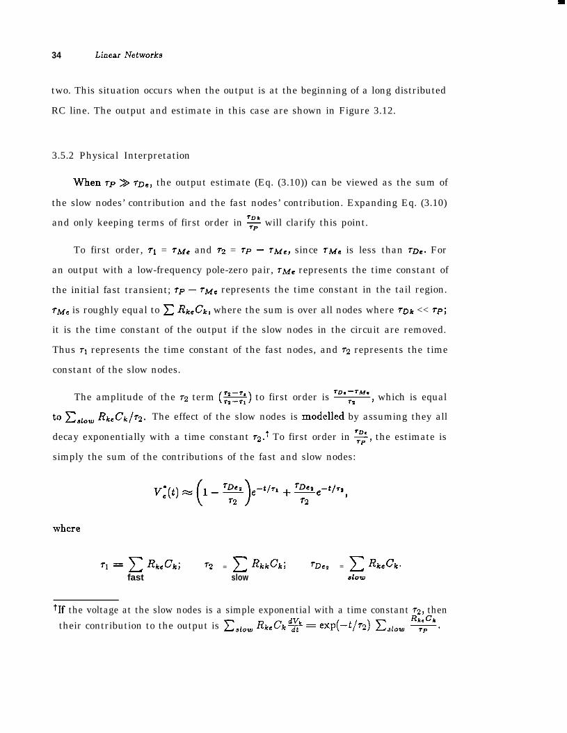
Figure 3.12 Output from the begining of a long RC line.
I
34 Linear Networks
two. This situation occurs when the output is at the beginning of a long distributed
RC line. The output and estimate in this case are shown in Figure 3.12.
3.5.2 Physical Interpretation
When TP >> TDe, the output estimate (Eq. (3.10)) can be viewed as the sum of
the slow nodes’ contribution and the fast nodes’ contribution. Expanding Eq. (3.10)
and only keeping terms of first order in F will clarify this point.
To first order, rr = rMe and 72 = ?p - rMe, since TMe is less than r&. For
an output with a low-frequency pole-zero pair, rMe represents the time constant of
the initial fast transient; rp - rMe represents the time constant in the tail region.
rMe is roughly equal to c &Ck, where the sum is over all nodes where rDk << rp;
it is the time constant of the output if the slow nodes in the circuit are removed.
Thus rl represents the time constant of the fast nodes, and 72 represents the time
constant of the slow nodes.
The amplitude of the r2 term (z) to first order is TDciZTM’, which is equal
to cslow &eCk/r2. The effect of the slow nodes is modelled by assuming they all
decay exponentially with a time constant 7z.t To first order in %, the estimate is
simply the sum of the contributions of the fast and slow nodes:
where
71 = c R&k; 72 = c RkkCk; TDez = c &e’%-fast slow alow
+If the voltage at the slow nodes is a simple exponential with a time constant 72, thenRksCktheir contribution to the output is ~Slow RkeCkg = exp(-t/T2) cslow 7.
3.5 Two-Time-Constant Model 35
3.5.3 Bounds Improvement when rp > rDe
When up is much larger than rDe, some capacitors decay slowly compared to
the output. The relationship between the output and the voltage at these slow
nodes changes as the output decays. Initially all the voltages start at the same
voltage. When the output voltage is small, the slow nodes’ voltage can still be quite
large, since they decay more slowly than the output. Using a single constant to
bound the voltage at these slow nodes in terms of the output voltage will be a poor
approximation of the actual node voltage, at least for some range of output. The
improved estimate overcomes this problem by grouping the slow nodes together and
letting them decay at their own rate. The output is then written as the sum of two
terms, one modelling the slow nodes, and the other modelling the rest of the tree.
The same idea of decoupling the slow nodes from the output is used to improve the
bounds.
To improve
upper bound on
the lower bound on the output, rp is improved by using a better
the internal nodal voltages:
This upper bound sets the voltage at the slow nodes to be 1 when the output voltage
is large, thus decoupling the slow nodes during the initial transient. The improved
bound on the output voltage becomes
where
T& c QkRkeCk; 7; 1 ak)RkkCk; 1, 2&e 5 Rkk;= = -
ak =k k
0, 2Rke > Rkk.
The upper bound on the output is more difficult to improve. Here the slow
nodes are decoupled from the output by replacing them by a voltage source. The
36 Linear Networks
value of the source is chosen to give an upper bound on the actual output. Super-
position is then used to write the bound as the sum of two terms, one caused by
the slow nodes and the other from the network minus the slow nodes. Assuming
the voltage source is placed at node V, the improved upper bound is
R TheV,<L+-e-t/T;
R 9 (3.12)vv T;e
where the starred time constants represent time constants for the modified network,
with the slow nodes shorted out by the added voltage source. Appendix C describes
these bounds in more detail.
3.5.4 Computational Requirements
In both the improved bounds and estimate, a small number of time constants
characterize the output waveform. Each time constant is a sum over all the nodes
in the tree. For a network with n nodes, each time constant takes O(n) time
to compute. However, unlike the original bounds, the terms being summed are
not shared by different outputs. The bounds are improved by tailoring the time
constants to a particular output. This difference means it takes O(n2) time to find
improved bounds for all nodes in an RC tree, rather than the O(n) time required for
the original bounds. If only a constant number of outputs need improved bounds,
then the time complexity remains O(n).
The improved estimate only depends on three time constants, rD,, rp, and TM~.
Figure 3.8 has already illustrated how to find the first two time constants for all
nodes in a tree in linear time. rMe also can be found for all nodes in linear time.+
Thus, both an estimate and an improved estimate can be found for all outputs in
O(n) time.
tDefine CL = C,(l - rDk/rp). C; can be found for all outputs in O(n) time.Thus determining TM, can be reduced to finding c C;&, for every node, a taskequivalent to finding rD, for all nodes in a tree.
3.6 Connecting Two RC Trees 37
3.6 Connecting Two RC Trees
The delay models derived in the preceding sections have always assumed that
a voltage source in series with a resistor drives the output network to its new
value. This approximation breaks down when the capacitance within a gate is not
negligible, or when a pass transistor turns on, connecting a new output net to an
already settled output. For these situations, the output net is driven by an RC
tree. This section derives timing models for these two-tree circuits. Like previous
models, an initial single-time-constant estimate and bounds are derived, and then
methods to improve these waveforms are discussed. Networks where the bounds
poorly approximate the actual output closely resemble the rp >> r& problem in a
single RC tree, and the same techniques can be used to improve the timing model.
Figure 3.13 shows a model of a two-tree circuit. It consists of tvo RC trees,
where an output, 7t, of the first tree connects to the input of the second tree.
As before, the voltages are normalized to range between 0 and 1, and the output
waveform for the falling edge is derived. For a falling transient, the root of the
first tree is grounded, and the second tree is precharged to 1. At t = 0 the switch
between the two trees closes. The voltage at any node in tree 2 can be written as
the sum of the voltages caused by each capacitor current:
v, = - c d&c,&n,~kl~ - C(R dVc,k&ree 1
nn1 + Rkez)Ckz -.dt(3.13)
kEtree 2
3.6.1 Single-Time-Constant Model
Both the estimate and bounds use the same formula derived for a single RC
tree; only the time constant definitions change. For a single-time-constant estimate,
d&/dt is replaced by akdV,/dt. Matching the integral of the estimate with the
integral of the real output again gives the best value of ok. Since nodes in tree
1 start and end at ground, their ok is zero. For nodes in tree 2, ilk is one. The
38 Linear Networks
Tree 1 Tree 2
e0
Figure 3.13 Two- tree model.
estimate is a decaying exponential with a time constant rb,:
v:(t) = exp(--t/r&); r’oe = C(Rnfzl + &ez)&.&2
For the single-time-constant estimate, tree 1 can be modelled by a resistor of value
Rnnl: the capacitors in tree 1 have no effect. Thus for the output estimate, internal
gate capacitance can be ignored if its voltage at the beginning and end of the
transient is the same; only capacitors that change voltage need to be modelled.
A bound on the output voltage can be found by integrating equation (3.13) as
was done in Section 3.4.2. However, the internal voltage bounds for the two-tree
network differs from the single-tree bounds. The single-tree bounds only apply
when the current from each capacitor, -CdV/dt, is positive. When two trees are
connected together, the nodes in tree 1 first rise and then fall. The only lower bound
for these nodes is vkI 2 0. Since the input of the second tree is always 2 0, a lower
bound for these nodes when the input is grounded will also be a lower bound in this
case: vk2 2 R%VI. Using these lower bounds gives rR, for a two-tree output:
rke = c (Rnn, + Rkez)Rkez cR ka *
kc2 -2
An upper bound for the internal voltages can be found by using the monotoni-
city of voltage along a path: V,, 2 vk if node k is downstream of node n. For
The transformed output voltage can then be represented as the sum of the
contributions of the slow group 2 nodes, U,,, plus the contributions of the faster
group 1 nodes, Ue,. The slow nodes will decay at a rate approximately equal to rp,,
so their contribution to the output can be estimated by+
u,, = - c Rke Ckdvk-%dt
F sech2(t/rpS).2
The contribution of the faster nodes is found by assuming all these nodes decay
at the same rate as the output:
ue, m- c dKRkeck-- = dKkE1
dt
To solve this equation, Ue, must be related to V,. For outputs with two time
Constants, Tp2 >> TDel, so ue, will be roughly constant during the decay of U,,.
Therefore U,, can be approximated by Ue -TDe2/Tp,. It is important to realize that
Eq. (4.15) d ffis i erent than the equation for a single-transistor driving a capacitance
load. The relationship between U, and V, depends on their values: the presence of
tFor the falling transient, V = 1 - tanh(t). dV/dt. is proportional to U, which issech2(t).
4.6 Two-Time-Cons tant Model
- - - - -- - - - - EstimateEstimate- -- - 2nd Order Est.2nd Order Est.-- RealReal
00 55 1010 1515 20 2520 25Time in RCTime in RC
Figure 4.6 Two-time-constant output waveform.
61
a dc voltage at the nodes changes the nature of the transient. Solving Eq. (4.15)
yields an estimate of Uel:
For the falling edge, the effect of the dc voltage is minor: the shape of the out-
put remains unchanged; only the time constant is changed.+ Combining the two
contributions to U yields the two-time-constant estimate:
sech2(at/rDe,) i- ? sech’(t/rp,)a
(4.16)
where
Figure 4.6 shows a two-time-constant output along with the original estimate
and the improved estimate. The improved estimate is a much better model of the
output waveform.
tFor the rising edge, the shape of the faster transient changes form. The s!ow modeis 1 - l/t while the faster mode is coth(t).
62 Nonlinear Networks
4.6.2 Bounds Improvement
For outputs where r,, << r&, the bounds can be improved by using better
internal voltage bounds to generate rae. For nonlinear circuits, the bound improve-
ment is a two-step procedure: first bound Uk in terms of Ue, and then from this
bound generate bounds on the actual voltage. A better lower bound on Vk can be
determined using a method analogous to the linear circuit technique described in
Section 3.4.5. The improved bound on U improves the bounds on V, which leads
to an improved r,,.
For outputs where rpe >> rDe, tighter bounds can be generated by following
the linear two-time-constant technique. The improvement of the lower bound is
identical to the method described in Section 3.5.3. This method simply uses the
constraint that Vk 5 1 to improve the upper bound on the internal voltages used
to generate rp,. The result is a set of time constants that provide a better lower
bound on the voltage.
Generating a better upper bound proves to be more difficult. Again the same
basic approach used to improve the linear bound can be applied to the nonlinear
network: a voltage is added to isolate the slow nodes from the output. By adding
the voltage source, the transformed output voltage can be written as the sum of
two terms. The voltage source causes one term, and the capacitor currents cause
the other. The effect the voltage source has on the output is easily determined; the
effect of the capacitor currents is more difficult to ascertain.
Like the fast transient in the improved nonlinear estimate, the output waveform
depends on the voltages present in the circuit (which result from the voltage source).
For a linear network these voltages are not an issue: by superposition the sources
can be considered one at a time. These dc voltages also affect the bounds that relate
the maximum change in V, to the change in V,. The bounds on the transformed
voltage at each node are identical to the bound on the voltages for a linear network:
4.7 Mixed Nonl inear Elements 63
Unfortunately the relation between U and V depends on the voltage. Bounds on
the voltages can still be obtained, but the dc voltages present at the node need to
be taken into account. Once a bound for the transient is obtained, the bound on
the transformed output voltage is the sum of the bounds on its two components.
The inverse transform of this sum yields an improved bound on the output.
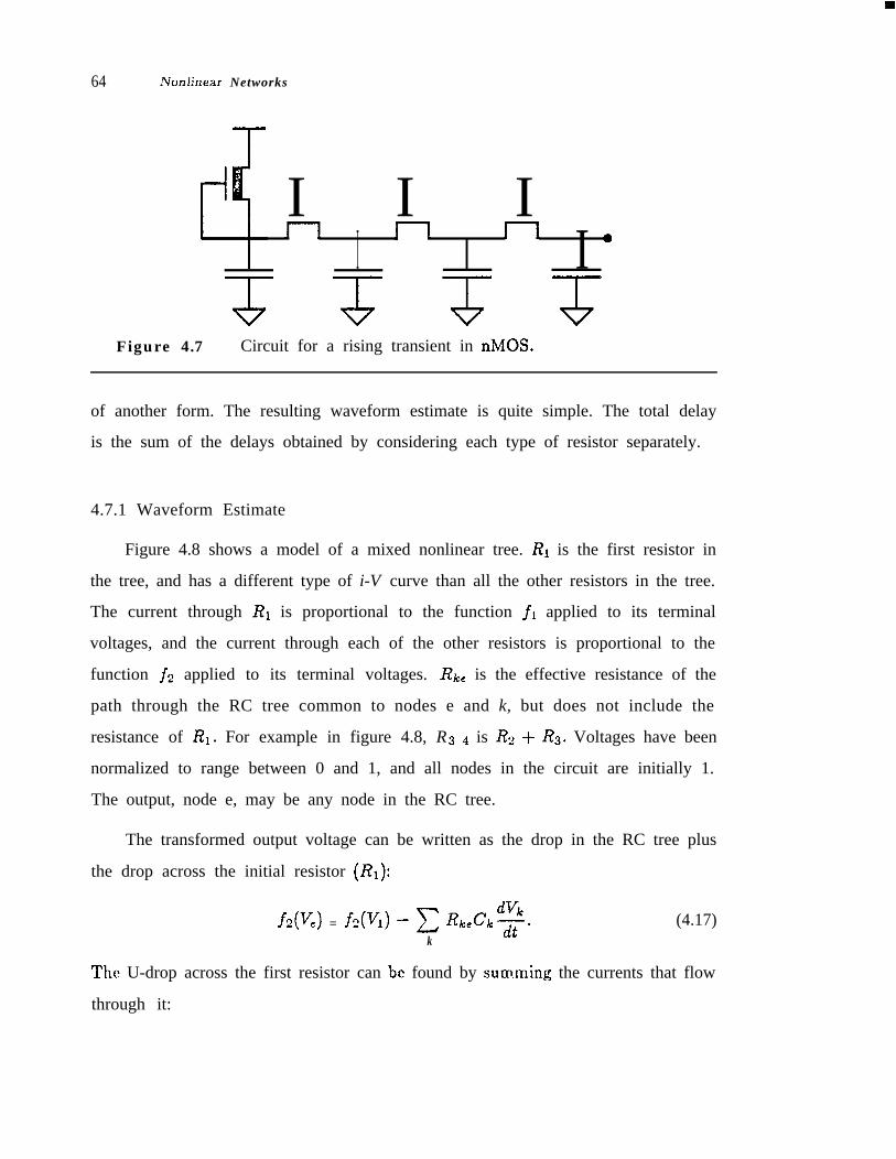
4.7 Mixed Nonlinear Elements
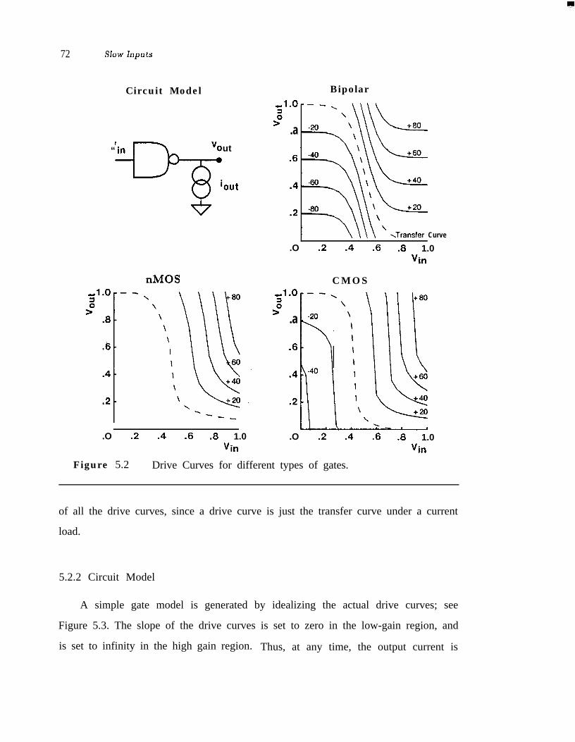
One limitation of the timing models that have been presented in this chapter
is the requirement that all resistors in the circuit must have the same form of i-V
curve. To generate a timing model for the rising output of an nMOS pass transistor
network driven by a gate (see Figure 4.7), either the depletion transistor must be
modelled as a pass transistor or the pass transistors must be modelled as depletion
transistors. This approximation causes a problem when the dominant resistance in
the circuit changes with time. For example, in Figure 4.7, if the resistance of the
depletion load is small compared to the pass transistor resistance, then the depletion
transistor does not have a large effect on the output waveform. A crude model of
this transistor can be used (for example, modelling it as a short) without causing a
large error in the output estimate.
A problem arises when the resistance of the depletion transistor is initially
large compared to the pass transistor’s resistance. When the output is low, the
dominant resistor is the depletion transistor. As the output rises, the resistance
of the pass transistors increases and they eventually control the output waveform.
The shape of the output cannot be modelled by either the depletion transistor or
the pass transistors alone. Each device affects a portion of the output. Timing
models for this type of circuit are generated by extending the basic timing model to
handle circuits where a resistor of one form drives an RC tree composed of resistors
64 Nonlinear Networks
I I II I ’
T T z J-Figure 4.7 Circuit for a rising transient in nMOS.
of another form. The resulting waveform estimate is quite simple. The total delay
is the sum of the delays obtained by considering each type of resistor separately.
4.7.1 Waveform Estimate
Figure 4.8 shows a model of a mixed nonlinear tree. RI is the first resistor in
the tree, and has a different type of i-V curve than all the other resistors in the tree.
The current through RI is proportional to the function jr applied to its terminal
voltages, and the current through each of the other resistors is proportional to the
function ji applied to its terminal voltages. Rke is the effective resistance of the
path through the RC tree common to nodes e and k, but does not include the
resistance of RI. For example in figure 4.8, R3 4 is Rz + RJ. Voltages have been
normalized to range between 0 and 1, and all nodes in the circuit are initially 1.
The output, node e, may be any node in the RC tree.
The transformed output voltage can be written as the drop in the RC tree plus
the drop across the initial resistor (RI):
fi(&) = h(v,) - c Rk.Ck$k
(4.17)
The U-drop across the first resistor can br found by summing the currents that flow
through it:
4.7 Mixed Nonlinear Elements 65
%
output
Figure 4.8 A mixed nonlinear circuit.
Substituting Eq. (4.18) in Eq. (4.17) gives
To generate a single-time-constant estimate, dVk/dt must be approximated by
a term proportional to dVe/dt. Setting v, equal to V, in Eq. (4.19) and rearranging
terms yields an estimate of the output waveform, Vt :
At = -rls
vz dV,s
v’ dV,1 flo - rDe 1 fi(ve)’
(4.20)
where
71 = c RI c/c; TDe = cRkeCk.k k
The estimated delay is the sum of two terms. The first term is the delay caused by
RI, assuming all the other resistors are replaced by a short circuit; the second term
is the delay through the RC tree assumin,d the first resistor is replaced by a short
circuit.
66 Nonlinear Networks
The integral of the difference between the transformed (using the function f2)
output voltage and the estimate is
The difference in the second sum is zero since V, and vk start and end at the same
voltages. The difference in the first sum is harder to quantify. The two terms
in the sum will cancel only when VI and vk are similar in value. However, the
contribution of RI to the integral of the transformed output is only significant when
RI’s resistance is large compared to the resistance of the RC tree. In this case, most
of the voltage is dropped across RI and therefore VI and vk will be roughly equal.
When the resistance of RI is small compared to the resistance of the RC tree, the
difference in VI and vk can be large, but the percentage error will still be small,
since the first term is a small fraction of the total output voltage.
As an example, consider a set of pass transistors driven by a linear resistor as
shown in Figure 4.9. The waveform estimate for this circuit is
1At = -ri ln(l - Vi) + TDep
1 - v : ’
The response is initially dominated by the resistor, but for large voltages the
pass transistors dominate. Since the estimate models both regions, it is a good
approximation of the actual output.
4.7.2 Bounds
To bound the output waveform, Eq. (4.19) must be integrated, since bounds for
the differential voltages are not known. This integral cannot be evaluated directly
since the relationship between vk and VI is not known. Instead, a bound for VI can
4.8 Summary
- - - Estimate- Real
0 5 10 15 20 25Time in RC
Figure 4.9 Output for a mixed nonlinear circuit.
67
be used to generate a bound on the integral. This bounded integral can then be
used to generate bounds on the output waveform. These waveforms bound both the
single-time-constant error and the error resulting from approximating the value of
V' in Eq. 4.19 by V,. Simply finding T,~ and rpc for the nonlinear tree is sufficient to
check the single-time-constant approximation: the presence of Rr (a series resistor
driving the tree) only makes these time constants closer to each other and to rDe.
If the bounds for the tree alone (assuming RI is 0) are good, then the single-time-
constant estimate will be a good approximation for the output.
4.8 Summary
Timing models based on linear RC trees have one fundamental drawback: the
uncertainty in the error caused by linearizing t*he transistors. To eliminate this
type of error, timing models have been derived for MOS resistor trees. Although
the out.put of general nonlinear circuits is difficult to estimate, the output of a MOS
circuit can be’modelled more easily, since all transistors and transistor combinations
have roughly the same shape of i-V curve.
68 Nonlinear Networks
For circuits where the i-V curves of all resistor and resistor combinations have
the same shape, a simple transformation of variables converts the nonlinear circuit
into a pseudo-linear circuit. The techniques used to derive an estimate and bounds
for linear networks can be applied to the transformed nonlinear network. Like the
linear models, the resulting timing models depend on three simple time constants. -
The timing model can be applied to MOS circuits by using a simple quadratic
model for a MOS transistor. The crucial difference between the nonlinear timing
model and the linear model is in the output waveform. An output estimate using a
linear transistor model is exponential, whereas an output estimate using a quadratic
transistor model has a (l- l/t) dependence for a rising t,ransient, and a 1 - tanh(t)
dependence for a falling transient. Linear models minimize the timing error caused
by the incorrect waveform by allowing a transistor’s effective resistance to depend
on the type of transient.
Outputs that are not dominated by a single slow mode have poor bounds.
A two-time-constant model provides a better estimate of these outputs. The key
difference between the nonlinear and linear improved estimate is that the faster
decaying component of the output in a nonlinear circuit may have a different time
dependence than the slow mode. In a linear circuit both components to the output
waveform are exponentials.
The timing model was extended to handle circuits that contain two different
types of nonlinear resistors; the delay through a mixed circuit is approximately the
sum of the delays obtained by looking at each type of resistor individually. For a
depletion load driving a pass network, the delay is the sum of the time it takes the
depletion transistor to charge the total capacitance plus the delay through the pass
transistor network.
Chapter 5
SLOW INPUTS
5.1 Introduction
Chapter 3 has presented a method for generating timing models for linear RC
circuits. To apply this model to MOS transistor clusters, two approximations must
be made: transistors must be modelled as linear resistors and the inputs to transistor
clusters must be modelled as step waveforms. Chapter 4 has eliminated the need
for the first approximation by presenting a method to derive timing models for
nonlinear networks. The goal of this chapter is to eliminate the need for the second
approximation: to generate an estimate of the output waveform for an arbitrary
input waveform. The need for this extension is shown in Figure 5.1; the shape of
the output waveform clearly depends on the shape of the input driving the gate.
Approximating all inputs by a step waveform will significant.ly underestimate the
gate delay for slow inputs.
For step inputs, a very simple model of a transistor can be used; the transistor
is either an open circuit or a fixed nonlinear resistor. When the input changes
gradually, the states between on and off must be modelled. Logic-gate drive curves
are one way to represent this information. Drive curves depict a contour map of
the gate output current versus input and output voltage. The shapes of all drive
curves are roughly the same and lead to a very simple circuit model for a gate. This
gate model reduces to the model used in Chapters 3 and 4, a resistor in series with
a switch, for fast inputs.
Using the gate model: the output waveform of a transistor cluster can be
determined as a function of the input waveform. The output of a simple gate is
70 Slow Inputs
.6
1 2 3 4 5 6t
.6
.4
.2
I ,0 1 2 3 4 5 6
t
Input Waveform Output Waveform
Figure 5.1 Gate output waveform for different input waveforms.
derived first, since this circuit only has a single time constant. The results show
that the output waveform is not very sensitive to the shape of the input: a simple
ramp model of the input is sufficient to determine the output waveform.
Next, the output of a general transistor cluster is estimated. For these cir-
cuits, the output network is an RC tree, and the output cannot be determined ex-
actly. However, the single-time-constant approximation converts a complex transis-
tor cluster into a simple gate, which allows the output waveform to be estimated. To
insure the single-time-constant approximation is valid, single-time-constant bounds
are also derived. The bounds are worst for quickly changing inputs and improve as
the input becomes slower. Thus, any output with good bounds for a step input will
have even better bounds when driven with a slower input.
5.2 Gate Models
Before a gate model can be constructed, the important characteristics of a gate
must be determined. A gate’s transfer curve, which shows the dc output voltage for
any input voltage, is only part of the information needed. The time behavior of the
5.2 G a t e Models 71
output voltage depends on the gate output current, since the current is what drives
the output to its new state. To find the output waveform, the output current must
be known as a function of input and output voltages. Drive curves are one way to
represent this information.
5.2.1 Drive Curves
The drive curves for a gate give a contour map of the gate output current
versus input and output voltages. Instead of plotting the input-output pairs where
the output current is zero, which gives the transfer curve, the output voltage vs.
input voltage is plotted for different output currents. The transfer curve is only one
curve in a set of curves.
Figure 5.2 shows the drive curves for CMOS, nMOS and bipolar gates. The
transfer curves for the three gates are similar. Comparing the drive curves shows a
more striking difference. The bipolar gate’s drive curves are spaced closer together
than those for the MOS gates, indicating a higher current gain. The output
waveform of a bipolar gate will not depend strongly on the input waveform since
the output current only depends on the input over a small range of input voltage.
For both nMOS and CMOS gates, the input can affect the output current over the
entire input voltage range. Consequently these gate types are more sensitive to the
shape of the input waveform than the bipolar gate.
The drive curves for all gates have a high gain region (magnitude of the slope
>> 1) and a low gain region, giving the curves an ‘L’ or inverted ‘L’ shape. This
shape is fundamental to all simple, level restoring logic gates. If a gate is able to
restore a degraded input signal, then the transfer curve of the gate must have a
gain much less than one near the dc output levels. These low-gain regions force the
remaining region to have a gain much larger than one because a gate’s input and
output voltage ranges are equal. The constraints on the transfer curve !ix the shape
72 Slow Inputs
Circuit Model Bipolar
“in “out
++3+iout
Ml.0:
> .a
.6
\Tr.ansfer Curve
nMOS CMOS-1.0:
> .a
.6
.O .2 .4 .6 .8 1.0Vin
.O .2 .4 .6 .8 1.0 .O .2 .4 .6 .8 1.0Vin “in
Figure 5.2 Drive Curves for different types of gates.
of all the drive curves, since a drive curve is just the transfer curve under a current
load.
5.2.2 Circuit Model
A simple gate model is generated by idealizing the actual drive curves; see
Figure 5.3. The slope of the drive curves is set to zero in the low-gain region, and
is set to infinity in the high gain region. Thus, at any time, the output current is
5 . 2 Gate M o d e l s 73
Figure 5.3
“a V in
Idealized drive curve and resulting gate model.
R
gm
if+
ideal
controlled by either the input or the output voltage, but never both. The circuit
model for a gate becomes a voltage-controlled current source when the gate is in
the high-gain region, and a resistor, when the gate is in the low-gain region. The
low-gain region is entered when the resistor current is lower than the output of
the current source. Both regions can be modelled by a resistor in series with a
current source, and two ideal diodes. The ideal diodes model the transitions from
the high-gain region to the low-gain regions. The current source pulls the output
toward ground when the input is greater than V,, the switching voltage of the gate,
and it pulls the output high when the input is lower than V,.
For a falling transient, the output remains clamped to the high output level
until the input rises to V,. After the input reaches V,, the output current changes
sign, and the top clamp diode turns off. The output enters the high-gain region
and the output current is controlled by the current source. When the output of
the current source becomes larger than Vout/R, the bottom diode shorts out the
current source and the current is controlled by the resistor. This circuit model is
not of necessity piece-wise linear: the current source and/or the resistor may be
nonlinear. This model of a gate makes it possible to determine the output for an
arbitrary input waveform.
74 Slow Input3
-1.0z
> .a
.6
1-L1.O .2 .4 .6 .8 1.0
Vin(a) Drive Curves
Figure 5.4 An nMOS gate model.
al.0gz .8
.6
- Real--. Model
12 3 4 5t
(b) Output Waveforms
By idealizing the drive curves, the effect of the output voltage on the output
current is ignored in the high-gain region. This approximation is valid when the
input and output time constants are comparable. For the same change in voltage,
the output’s effect on the output current is A,, times smaller than the input’s
effect, where A,, is the slope of the drive curves. Ignoring the output’s contribution
completely does not cause a large error. t The drive curves for a nMOS gate along the
model drive curves are shown in Figure 5.4a; the output waveforms for two different
inputs are shown in Figure 5.4b. The fit to the output waveform is excellent,
indicating the approximations made to generate the gate model do not cause a
large error in the output estimate.
Using this model, a gate is characterized by four parameters: the gate’s switch-
ing voltage, V,; the gate’s forward transconductance in the high-gain region, gm;
tFor very slow inputs, this achanges much faster than tfl
proximation breaks down. The output voltage nowe input, and its contribution to the current can no
longer be ignored. Although the error in the ,ate dela increases as the inr 2 P
utslows down, if the error is measured relative to tie t.otalof the gate driving the in ut, then the
elay, including the de ay
slow inputs. Stated simp y, the inputP aercentage error actually decreases for veryelay swamps the total.
5.3 Simple Gates 75
n
-=lo.dJFigure 5.5 A simple gate.
gm ‘load
and the output resistance in the low-gain region for the rising (falling) waveform,
R, (Rf). In general both g,,, and R, (Rf) can be nonlinear.
Finally, this simple gate model reduces to the gate model used in Chapters 3
and 4 for a step input. When a gate input changes from a 0 to a 1, the output
current instantly changes to its maximum value. This maximum current is greater
than or equal to the largest current through the output resistance, so the gate
immediately enters the low-gain region of the drive curve. The gate model becomes
a simple (nonlinear) resistor, Rf, which is the model used in the previous chapters.
5.3 Simple Gates
A simple gate is one where its output network is a single capacitor; see Figure
5.5. These gates have only a single time constant, and their output for an arbitrary
input can be found exactly. The model shows that the output waveform is only
weakly coupled to the shape of the input waveform. A qualitative description of the
output is given first, followed by a quantitative description of a linear-gate output.
Using the linear gate as a guide, the output waveform of a nonlinear gate is derived.
The nonlinear model is then applied to MOS gates, and their characteristics are
discussed.
76 Slow Inputs
5.3.1 Qualitative Analysis
For a rising input, the output remains high until the input reaches the switching
voltage of that gate. The initial shape of the input waveform has no affect on the
output. After the switching point is reached, the input voltage controls the output
current. The output voltage in this region is 1 minus the integral of the output
current. The output current, and therefore the slope of the output voltage, increases
monotonically until the output enters the low-gain region of the gate. At this point,
the output voltage again becomes independent of the input, and decays to 0 with a
time constant determined by the gate’s resistance (Rf) and the output capacitance
(Cload). The shape of the initial and final sections of the input waveform do not
have any affect on the shape of the output. This decoupling means that a minimum
of information about the input waveform is needed to determine the output of a
gate. Usually, the slope of the input when it crosses the gate’s switching voltage is
sufficient.
5.3.2 Linear Gates
Linear gates are the simplest to analyze, since both the output resistance and
the voltage-controlled current source are linear. First, the output waveform for a
linear gate driven by a ramp input is derived. From this analysis, the gate delay
can be found as an explicit function of the input slope and the gate parameters. To
determine if a ramp can be used to model the actual exponential input waveforms,
the output waveform for an exponential input is determined. The resulting output
is quite similar to the output for a ramp input, as long as the slopes of the two
input waveforms are the same at the switching voltage of the gate.
In the following derivation, the input and output voltages have been normalized
to range between 0 and 1, and the switching point of the gate is V,. Since the rising
and falling transients are similar, only the falling v;aveform is discussed. The input
5.3 Simple Gates 77
transconductance has been normalized by the output resistance to yield the factor
p = (gmR,)-l. The value of /? ranges between 0 and 1 - V,, and represents the
range of input voltages where the output current is determined by the input. The
quantity V, + p is the highest input voltage that can affect the output current.
Gates with smaller p have higher current gain, and are less sensitive to the input
waveform than gates with larger ,8. Finally, the intrinsic time constant of the gate
is rf = RfCIOad. For a step input, the output is a decaying exponential with a time
constant 7f.
A ramp input will be represented by
so the input is equal the switching point of the gate at t = 0. The slope of the
input is controlled by CY; it takes cyrf for the input to rise from 0 to 1. For this
input voltage, the output current is a ramp, and the resulting output voltage is
t2v l--out = 2apr2f * (54
The output voltage is given by Eq. 5.1 until the output enters the low-gain region
of the drive curves. This transition occurs when the voltage drop across the series
resistor, ioUtRf, is equal to Vout, and the time when this occurs will be called t,:
t, = Tf [dTTz& 11.
After t, the output current is determined by the resistor, and the output exponen-
tially decays to 0. The resulting output waveform begins as a quadratic, and ends
as a exponential: I 1 -- 2CYpr2f t2 ’ 0 5 t 2 t,;Vbut(t) =(1-&)exp(y), ’ t. 5 t. (54
78 Slow Inputs
Gate Delay Output Slope,2.5-
I 40 1 2 3 4 5 6 0 1 2 3 4 5 6 7 8 910
4 4Figure 5.6 Gate delay and output slope versus input ramp rise time.
The gate delay, td, is defined to be the time required for the output to reach
V, after its input reaches V,, so the delay through a series of gates is simply the
sum of the individual gate delays. From the output waveform, both the gate delay
and the output’s slope at the switching voltage can be found:
td =
where oP,,it = 2(1- VJ/V;. F gi ure 5.6 shows a plot of the gate delay and output
slope as a function of cup for V, = .5. The gate delay can be approximated by the
simple formula:
td = Tj J(ln Vs)2 + 241 - Vd)
It is not surprising that the importance of the input slope is determined by thetsize of a,B. This product represents the amount of time (measured in units of rf,
5.3 Simple Gates 79
the intrinsic gate delay) that it takes the output current to change from zero to
full scale, since [Y is the number of time constants the input takes to change from
0 to 1, and p is the voltage range that must be crossed to turn the output current
fully on. When cup is much less than one, the current changes rapidly compared
to the output, and the output waveform is a simple decaying exponential. When
cup is much larger than one, the output current is limited by the input, and the
gate delay increases. The increase in delay is caused by slowing down the initial
fall of the output waveform. The shape of the output waveform for low voltages is
unaffected by the input slope, except for very slow inputs.
Another way to view the gate delay is as the sum of two terms: one is the
intrinsic delay of the gate, the other is the delay caused by the input. Rewriting
Eq. (5.5) in terms of the inverse of the input slope, setting rim = crrf gives
td = Tf In Vd)2 + 2TinTg(l - Va), (5.6)
where r9 = &md/6n is the time constant associated with the current source.
Since the output waveform for a falling transient looks exponential at low
voltages, the rising output of a gate will be exponential at high voltages. Therefore,
to find the output waveform at the end of a series of gates, the output for an
exponential input must be determined. The derivation for an exponential input is
similar to the derivation for a ramp. t Figure 5.7 shows the delay versus Tin, the
time constant of the exponential input, for a gate with /3 = V, = .5.
The delay for an exponential input given in Figure 5.7 is almost identical to the
delay for a ramp input, Eq. (5.5), if the slope of the ramp is set to the slope of the
exponential at the switching point of the gate. This result is not surprising, since
+For an exponential input the time when the gate enters the low-gain region cannotbe found explicitly. Instead an implicit relation must be used: both t, and ri,r (theinput time constant) are found as a function of the output voltage at t,, Ve(ts).
80 Slow Inputs
.5
t
0 1 2 3 4 5 6GdTf
Figure 5.7 Gate delay for an exponential input.
the output is only affected by a narrow region of the input voltage. For slow input
transitions, an exponential differs significantly from a ramp only after the output
enters the low-gain region of the drive curve. When the input affects t.he output,
the two waveform are nearly identical. The input shape has the largest affect on the
output voltage when the input and output time constants are roughly equal; even
in this case the difference in gate delay in Figure 5.7 and the delay for a ramp is
less than 10 percent. Thus, the gate delay given in Eq. (5.5) is valid for exponential
inputs when CY is set equal to rin/(rf(l - Vs)), th e inverse slope of the exponential
input.
Since Eq. (5.5) (or Eq. (5.6)) is valid for exponential inputs, it provides a delay
model that can be used to determine the delay through a series of gates: the total
delay is the sum of the gate delays, when each d&y is found using the slope of its
input waveform. The next section extends this timing model to handle nonlinear
5.3 Simple Gates 81
gates, and Section 5.4 shows how to apply this timing model to gates with complex
output networks.
5.3.3 Nonlinear Gates
The technique used to derive the output for a linear gate can be used on
nonlinear gates; the nonlinearity just makes it more difficult to find t,, the time
when the output enters the low-gain region. As was done for linear gates, all
voltages have been normalized, and the falling output waveform is derived. The
output current of a nonlinear gate can be written as the minimum of the nonlinear
current source,
Zout = h?d7(L - v,),
and the nonlinear resistor current,
Zout = +(Kut,.
Rf is defined to be e, so f( 1) = 1, and g,,, is defined to be e v , so the slope
of g(0) is 1. Using these definitions, /I = (g,,,Rf)-’ is the maximum Lange of g(V)
where the input affects the output, and rf = RfCioad is the intrinsic time constant
for the falling waveform.
While the output is in the high-gain region, the output voltage is simply 1
minus the integral of the output current:
v 1-L st
out = Pq 0 g(K&) - K) &
The gate enters the low-gain region when the resistor current equals the input
current, i.e., t, is the solution to
t, : Pf(L&)) = g(Kn(k) - K)’
82 Slow Inputs
The output waveform after t, is the solution to the single-time-constant nonlinear
RC problem, T(t/rf).
The effect of the nonlinear transconductance can be visualized by creating
another circuit with a linear g,,, and distorting its input so the output currents
of the two systems are equal. To maintain equal currents, the distorted input is
K + S(vim - Va). Since the slope of g(0) is one, the distorted input looks similar
to the actual input around the gate’s switching point. As was previously shown,
the shape of the input is only important near the switching point. Thus, gentle
nonlinearities in transconductance do not have a significant effect on the output
waveform.
For an input waveform where g(Vi, - Vd) is a ramp,
vi, = v, + g-‘(t+,),
the initial output is identical to the output of a linear gate driven by a ramp:
t2v ‘ l - -out = 2ap72f *
The resistor begins to control the output current when the voltage drop across the
resistor becomes equal to the output voltage. Although it is difficult to determine
this transition time (tb) as a function of the input time constant, t, and CY can be
found as a function of Vout(ta), th e output voltage at the transition time’:
2 1 - v,ut(t,)Q = F [r(Lt(L>)121 1
The waveform after t, is
VOUf = qt/q - to); to = : - F(V,,t(t,)).
5.3 S imple Gates 83
This gives a gate delay of
td =
Like the delay through a linear gate, this delay can also be approximated by a
simple formula:
td = Tf II[T-‘(K)]2 + 2@(1 - I/#). (5.8)
5.3.4 MOS Gates
A MOS gate is nonlinear since both the input transconductance and the output
resistance are nonlinear. Surprisingly, these nonlinearities have only a small effect
on the output waveform: the output of a MOS gate is very similar to the output of
a linear gate.
Figure 5.8 shows the pulldown current versus input voltage for an nMOS
inverter; the curve for CMOS is similar. The transconductance increases slightly
with increasing gate voltage. This nonlinearity results from the quadratic relation
between gate voltage and drain current for a MOS transistor. The output current is
not proportional to the input voltage squared, since the gate’s output current is the
difference between the pullup and pulldown transistor currents. The nonlinearity
is reduced even further when high-field effects on the transistor are included. The
result is that the output current has only a small deviation from a linear gm. This
nonlinearity has a small effect on the output waveform and will be ignored.
The nonlinear output resistance sets the shape of the intrinsic output waveform.
For nMOS and CMOS gates, the nonlinear resistor leads to falling waveforms that
84 Slow Inputs
25 -
.O
Figure 5.8
.2 .4 .6 .6 1 .oInput Voltage
Output current vs. input voltage for an nMOS gate.
are roughly l-tanh(t) dan rising waveforms that are tanh(t).t The change in output
waveform has only a small effect on the gate delay. Using a simple quadratic model
for a transistor, with T/dd = 5v, and Vth = lV, f(V) for a MOS gate is
1 .8 V;f(V)
5=
1 -(l -V/.8)2 0 2 v 5 .8.
For this f(V),
1 - tT(t) =
0 5 t 5 .2;
.8(1 - tanh(tl.8 - .25) .2 2 t.
Using this function of T(t), in Eq. (5.5) gives the falling gate delay:
tThe rising waveform is for a depletion load in nMOS and for a p-channel transistorin CMOS. Actually the output waveforms are not tanh(t) for the entire outputrange. For a step input, the output initially ramps down untii the transistor leavesthe saturation region. After this initial ramp, the output deca,ys with a 1 .- tanh(t)time dependence.
5.4 Complex Gates 85
Since an nMOS inverter operates with a pulldown device overpowering the
pullup, its drive curves are asymmetric; see Figure 5.2. The switching voltage of the
gate, V,, is located below half scale and the series resistance for the rising transition,
R,, is much larger than the resistance for the falling transition, RI. This difference
in series resistance affects both the gate’s input sensitivity and its delay. Since the
resistance determines the intrinsic output time constant, the rising output will, in
general, be slower than the falling output. In addition, the large series resistance,
R,, and relatively large g,,, limit the range of voltages where the input affects the
output current for a falling input. Together, the low sensitivity to falling inputs
and the generally slow rising outputs in nMOS cause the input’s effect on the rising
output waveform to be small, but its effect on the falling output to be important.
The drive curves for an nMOS NOR gate are similar to the drive curves for
aninverter. If only one of the inputs is on, the presence of the other inputs has no
effect. The drive curves for an NAND gate differ from those of an inverter. The
gm of the gate is similar to the inverter; however, the series resistances, R, and
Rf, are n times bigger, where n is equal to the number of inputs. This increase
in series resistance increases the intrinsic gate delay, rf = RfCload, as one might
expect, but it also decreases the gate’s sensitivity to input waveforms. The increase
in series resistance decreases /3, the range of voltages where the input affects the
output, by n. The result is the input must be n times slower relative to the output
to cause the same relative effect on the output, or n2 times slower than the input
to an equivalent inverter.
5 .4 Complex Gates
When the output network of a gate is an RC tree, directly calculating the
output waveform becomes difficult. To find the output waveform involves solving a
set of differential equations. The single-time-constant approximation - assuming
86 Slow Inputs
Gate I Output Net I
Figure 5.9 Circuit model for a complex gate.
all nodes decay at the same rate - reduces this complex problem to one of finding
the output of an equivalent simple gate. To insure the errors in the estimate are
small, bounds are also derived. When the bounds are close to the estimate, the
errors in the single-time-constant approximation are small. When the upper and
lower bounds are very different from each other, a multiple-time-constant estimate
may be required.
Figure 5.9 shows an example transistor cluster. It consists of a gate driving
an output net, which is modelled by an RC tree. The output waveform for node e
in the RC tree is derived. The problem of finding the output waveform is similar
to finding the output waveform for a grounded RC tree, which has been discussed
in Chapters 3 and 4. However, the problems are not identical, since the RC tree
is driven by a current source during part of the output. First an estimate of the
output waveform for a linear tree is derived, and then the results are generalized
to include nonlinear RC trees. Bounds on the output are a!so derived.
5.4 Complex Gates 87
5.4.1 Waveform Estimate
For a current source drive, the sum of the capacitor currents in the tree must
be equal to the drive current:
i ( t ) = -cflk
Ck-$ (5.10)k
A single-time-constant estimate for the output voltage is found by assuming all
nodes decay at the same rate: s is equal to g. This gives the estimated output
voltage, V:, while the gate’s output is in the high gain part of the drive curve:
v:=1-s, i(r) dr
CT ’(5.11)
where CT is equal to the sum of the capacitors in the RC tree. To determine when
the gate’s current becomes limited by the resistor, the voltage at the output of the
gate must also be found. The voltage drop between V, and the gate’s output in a
linear tree is
v, - Ilou* = - cdvkRkc6c -
kdt ’
Again using the single-time-constant approximation, this voltage difference can be
related to s, which is &/CT:
v* V: - R,i,,,; R, = ck RkeCko u t =
ckck ’
The output enters the low-gain region when the voltage at the output of the current
source equals 0. This transition occurs when (Rf + R,)iout = V:. Once the gate
current is determined by the series resistance, the problem becomes identical to
estimating the output of a grounded RC tree. The resulting output is a decaying
exponential, with a time constant r&:
TDe = C(Rf + R/&c = (Rf + R,)CT*k
88 Slow Inputs
Figure 5.10 Conversion from a complex gate into a simple gate.
The estimated output voltage, V:, is identical to the output of a simple linear
gate, where the load capacitance of the simple gate is equal to the sum of all
capacitors in the RC tree, and where the series resistance of the simple gate is
equal to Rf + R,. The transconductance of the simple gate is gmr the value of
the original gate. Using the single-time-constant approximation converts a general
transistor cluster into an equivalent simple gate; see Figure 5.10. The delay through
a complex gate is approximately
td = [TDe In( •t ‘JTinTg(l - VY) (5.12)
where the input slope at V, is l/Tin. The delay is composed of two terms: one
represents the intrinsic delay of the gate and the other represents the delay caused
solely from the input. The value r& ln(Vs) is the cluster delay for a step input. This
is the delay predicted by the models in the previous chapters. The other term is the
cluster delay if all the resistors in the circuit are set to zero. Then, the time required
for the current source to discharge all the capacitors to V,, J2rinrg(l- V,), sets
the delay.
The timing model for complex linear gates can be extended to cover MOS
transistor clusters because these circuits can be transformed into pseudo-linear
networks. Since the derivation is analogous to the complex linear gate derivation,
it is only reviewed here. The single- time-constant approximation is again used
to convert a complex transistor cluster into a simple gate. The nonlinearity just
makes the resulting simple gate nonlinear. All resistors, including the gate’s output
5.4 Complex Gates 89
resistor, are assumed to have the same type of nonlinearity. When the gate’s output
resistor has a different type of nonlinearity, then the estimate becomes a mixed
nonlinear problem and can be solved using the method described in Section 4.7.
The current through a nonlinear resistor will be written as
where R,ff is the effective resistance of the device. As was described in Chapter 4,
this device appears linear if a transformed voltage, U = f(V), is used instead of
V.
For a current source drive, the constraint on the output tree is only on its
current; the estimate for a nonlinear circuit is the ,same as the estimate for a linear
gate (Eq. (5.11)). For a nonlinear circuit, the gate output voltage must be found
by estimating the U-drop .in the output net:
6 - Uout = c dVkheck -a
k dt
Again using the single-time-constant approximation, this U difference can be found
as a function of current:
u;,, = U: - R,i,,,; R, = ck RkeCk
ckck ’
The input loses control of the output current when the voltage drop across the
current source becomes 0. This transition occurs when (Rf + R,)i,,t = f(V,*).
After the output resistance of the gate takes over, the problem becomes identical to
finding an output for a grounded nonlinear tree. The resulting output is T(t/rDe),
where T(t) is the solution to the nonlinear RC network, and rDe is C(Rf + Rke)Ck.
Like linear complex gates, the estimated output voltage is identical to the
output of a simple gate, but for nonlinear output networks, the simple gate is also
90 Slow Inputs
nonlinear. The load capacitance of the simple gate is CT, and the output resistor
has an effective resistance of R, c Rf .
5.4.2 Waveform Bounds
To generate bounds on the output waveform, Eq. (5.10) is integrated and then
the v, are replaced by bounds in terms of V,. This substitution yields bounds on
the output voltage. First bounds for a linear network are derived and then they
are extended to model nonlinear circuits. Integrating Eq. (5.10) yields
/
tc Ckvk = CT - iout dr
k 0(5.13)
Bounds on vk are found by assuming all the current flows to node k (giving on
upper bound on vk) or node e (giving a lower bound on vk). For a linear network
this gives:
v, - (Ree - &&out 5 ‘vk 5 v, + (Rkk - &&out.
Using these bounds in Eq. (5.13) gives bounds on the output voltage:
CTV, >_cT -/
t
iout dT - iout(W - 7De);0
/
t
CT& <CT - io&) dT + iout(&(Ree + Rf) - %e);0
(5.14)
where
rp = C(Rf + &k)Ck; TDe = C(Rf + Rke)Ck.k k
These bounds on V, hold until the gate enters the low-gain region of the drive
curves. The transition time depends on the voltage at the gate’s output, Vout. Since
this voltage is not known exactly, the transition time must also be bounded. For
the lower bound on the tree’s output, the gate current should be maximized, so the
gate’s output voltage is set at its upper bound, Vour = V,. The latest time the gate
5.4 Complex Gates 91
could enter the low-gain region is when
K(b) = Rfiou&,).
An upper bound on V, requires the gate current be minimized, which in turn requires
that the gate’s output voltage be as low as possible: Vout = V. - (R,, + Rt)iout .
The earliest the gate could enter the low-gain region is
V&J = (Rf + &e)iout(t,m)
After the transition has occurred, the waveform bounding problem reduces to
finding bounds for a grounded RC tree. This problem is similar to the one solved
in Chapter 3, the primary difference being that the initial voltages in the tree are
not equal. The resulting bounds are
K I Ve(LJexP((ts, - WP), t 2 t&.
where
TRe = ctRf + Rke)2 ck
;x(Rf + Rkk)Ck.
k Ree rp = k
The bounds are continuous at the transition time.
For a ramp input, Vi, = V' + t/Tin, the bounds on the output are initially
t21
( TP - rDe)t (tRee + Rf )cT - dt- - - 1 .
2TinTg rinrg
c5 15j.TinTg
After t,, the output bounds are simple decaying exponentials:
(Rf&)ts, v < (Ree + Rf)@ts,e- (5.16)
rinrg rinTg
where
92 SIow Inputs
t ( 2rinrg61 = rp-
(*P - TDe + Tf)”
The bounds, the estimate and the actual output for the circuit shown in Figure
5.11a are shown in Figure 5.11b (rin = 270,) and Figure 5.11~ (rim = 10’~~~).
The bounds on the output waveform depend on the same three time constants
that define the bounds for a step input: rD,, r&, and rp. If the output has good
bounds for a step input, the case where rRe roughly equals rp, then the bounds for
a continuous input also will be good. It is not difficult to show that the bounds are
worst for a step input. Slowing down the input makes the bounds closer together,
since with a slow input the output is controlled by the input current source, which
is known, and not by its intrinsic time constants, which must be bounded.
The derivation for a nonlinear circuit follows the derivation used for linear
circuits. The output bounds are found by bounding vk by I< in Eq. (5.13). For
a nonlinear circuit, the bounds on vk are generated from the bounds on uk. The
latter can be determined by looking at the current flow in the tree:
ue - (R,, - &&out < uk 5 ue + (&c/c - Rke)iout.
These bounds can be converted to yield bounds on the nodal voltages. Using the
voltage bounds in Eq. (5.13) yields bounds on the output voltage. The output
bounds have the same form as the linear bound, but the definitions of the time
constants differ.
The gate’s U output can be bounded in terms of U,: providing a method of
bounding when the gate enters the low-gain region:
f(K(&)) = Rfiout(ts,);
f(K(tsu)) = (Rf + &e)~ou&,).
After this transition occurs, bounding the output reduces to finding bounds for a
grounded, (possibly mixed) nonlinear RC tree. The resulting bounds have a T(r)
.6
5.5 Summary
2fjifk5s~4$ut
(4 circuit
. - - Estimate- - Upper Bound
0 5 10 15 20Time in RC
(b) Normal input, rin = 27~~
0 5 10 15 20Time in RC
(C) SlOW input, Tin = 1070,
Figure 5.11 Output of a Complex gate for different input slopes. rDc =6, rg = 1.5.
93
shape, the output of the single nonlinear RC circuit. Like linear networks, the
bounds on the output waveform are worst when the input to the gate is a step.
5.5 Summary
The timing models presented in Chapters 3 and 4 were derived assuming the
input to a transistor cluster was a step waveform. This approximation allowed
one to determine the intrinsic delay of the cluster. Unfortunately, these timing
models cannot accurately determine the output of a transistor cluster, since the
input waveform is rarely a step.
94 Slow Inputs
To remove this limitation, this chapter has used a more complete gate model
to determine the effect of input shape on the output waveform. The drive curves of
a gate, a contour map of the gate output current versus input and output voltage,
provide the basis for this improved gate model. The output range of a gate can
be divided into two regions. In the high-gain region, the output current is mainly
controlled by the input voltage; in the low-gain regions the output current is mainly
controlled by the output voltage. By neglecting the effect of the output voltage in
the high-gain region and the effect of the input voltage in the low-gain region, a
simple gate model has been derived. This simple gate model reduces to the resistor
model used in Chapters 3 and 4 for step inputs.
Using this gate model, the output waveform dependence on input waveform
has been determined. For a simple gate, one with a purely capacitive load, the
output can be determined exactly. The output waveform is not strongly coupled to
the input waveform. For fast inputs, the input shape is irrelevant: the intrinsic gate
time constant controls the output. waveform. For slow inputs, the input changes
only slightly during the output transient, and again the shape of the input is not
very important. The output waveform can be determined using only a first order
approximation to the input, Vi, x V’ + t/Tin. The gate delay can be approximated
by the square root of the sum of the squares of two terms: the intrinsic delay of the
gate (for a step input) and the delay caused by the input waveform assuming the
intrinsic delay is zero.
The single- time-constant approximation has been used to convert complex gates
into an equivalent simple gate. Thus, the timing models derived for simple gates
apply to complex transistor clusters as well. To check the accuracy of the single-
time-constant approximation, bounds on the output, waveform have been derived.
The bounds are tightest for very slow inputs and become worse as the input becomes
faster. The worst bounds are for a step input, where they are equivalent to the
5.5 Summary 95
simple bounds derived in Chapters 3 and 4. If the bounds for a step input are good,
the bounds for a continuous input will also be good.
Using this timing model, it is possible to find the delay through a complex
transistor clusters. Thus, these timing models can be used to solve the problem
posed in Chapter 1: they can be used to find the delay through a complex MOS
circuit by determining the delay through its transistor clusters.
Chapter 6
CONCLUSIONS
To determine the delay through a large MOS circuit, the delay through the
transistor clusters that compose the circuit must be found. The timing models
used to determine the cluster speed must be simple, since an integrated circuit can
contain tens of thousands of clusters. Currently, timing analysis tools use empirical
models to estimate the cluster delay.
This thesis has presented a new timing model that retains the simplicity of
previous models, but is firmly grounded in the governing physics of the circuit.
This coupling between the model and the actual circuit eliminates the need to base
the output estimate on empirical results. Since the approximations used to derive
an estimate of the output waveform are explicit, the maximum error caused by
these approximations also can be determined. The coupling between the estimate
and the circuit physics provides more than just error control; it provides a way to
view MOS circuits so performance questions are easy to answer.
The timing model was developed in three stages, which is illustrated in Figure
6.1. First came a linear timing model. Here transistors were approximated by
linear resistors, and the inputs to a transistor cluster were approximated by step
waveforms. The model of a transistor cluster became an RC tree, and its output
waveform could be estimated using the single-time-constant approximation. The
accuracy of the single-time-constant approximation could be checked by deriving
waveform bounds, but the bounds did not check the validity of the other two
approximations. Figure 6.lb shows the output of this model.
The timing model was improved by applying the single-time-constant approx-
imation directly to a nonlinear MOS RC tree, eliminating the need to model each
98 Conclusions
05:;4
3
2
1
0
aI4E=s3
2
1
Circuit
1
10 2 0 3 0 4 0 50t hs)
(a) Input
--.- Model- Real
1 4
0 10 20 30 4 0 5 0t Ins)
(c) Nonlinear Model (Ch. 4)
i”5>3
2
1
----- Model- Real
II 4
0 10 2 0 3 0 40 5 0t (ns)
(b) Linear Model (Ch. 3)
tk40=s3
2
1
----- Model- Real
I 80 10 20 30 40 50
t (ns)(d) Full Model (Ch. 5)
Figure 6.1 Output estimates of the timing models.
6.1 Future Work 99
transistor as a linear resistor. Again bounds were derived to check the validity of
the single-time-constant approximation, leaving only the step input approximation
unchecked. Figure 6.1~ shows the output of this model.
Finally, a new gate model was developed based on the drive current of a gate.
This model together with the single-time-constant approximation provided a simple
method to estimate the output waveform of a transistor cluster for an arbitrary
input waveform. Since the approximations used to derive the output estimate are
explicit, the range of circuits where this model will be valid is also known. Figure
6.ld shows the output of this model.
6.1 Future Work
The models presented in this thesis show how to analyze most MOS circuits,
but suffer from two limitations: 1) the models assume the dc voltage levels of the
signals are known, since the model output is in normalized voltage, and 2) the
models assume the output of a transistor cluster does not affect its input.
The dc voltage range for the timing models can be found by first performing
a static analysis of a circuit. The static analysis must be able to find the voltage
range for every signal in the circuit, as well as determine the switching point of every
gate. This analysis is useful in its own right, since it provides a method to check
other aspects of circuit design, for example, noise margins and power dissipation.
Once the voltage swings are known, the timing models presented in this thesis can
be applied to a broad class of circuits,’ including cascade amplifiers and voltage
clamped busses.
The other limitation of the timing models is the requirement that the input
waveform be independent of the output. The output is determined as a function of
the input, but there is no way to determine the output when the input also depends
on the output voltage. This situation occurs in circuits that use positive feedback
100 Conclusions
to increase circuit performance, such as bootstrap drivers and sense amplifiers. To
analyze these types of circuits, the single time constant approximation must be
extended to handle circuits that contain multiple transistor clusters.
6.2 Final Thoughts
If the two limitations of the timing models are removed, the models should
be powerful enough to analyze all MOS circuit forms. The performance of a MOS
circuit only seems to depend on a few factors: the voltage swing, the type of non-
linear devices present, and the effective single-time-constant - a number which can
be found easily from the circuit. This improved understanding of the factors that
affect circuit performance is the most important result of this work.
Appendix A
VOLTAGE BOUNDS IN RC TREES
A.1 Simple Bounds
For a falling transition, all nodes in an. RC tree monotonically decrease with
time [wy82] and therefore current flows from every capacitor to the root of the tree
(ground). Because the current sourced from every capacitor is positive, the current
flowing along a path is guaranteed to increase monotonically and the voltage along a
path will decrease monotonically as one gets closer to the root. Using these results,
it is possible to bound one voltage in an RC tree in terms of another.
To bound the voltage at node k by the voltage at node e, define node n to be
the last node on the path to both nodes e and k. Then
vk>% -K > v,
R -R,,; Rnn = he;nn
and
v, 2 vn; J- > 5.Rnn - Rkk
Combining the first set of inequalities gives a lower bound on I$; the second set
gives an upper bound:
In the general case, if some function of the voltage, U = f(V), is proportional to
the current, then the bounds become
(A.2).
102 Voltage Bounds in RC Trees
A.2 Improved Bounds
The above bounds were generated using only information about the sign of the
capacitor currents; the bounds did not use any information about the time behavior
of the currents. Using this information leads to improved voltage bounds.
For the falling transition in an RC line,
when ‘node Q is downstream of node n. At t = O+, dVk/dt is 0 except at the first
node, where it is negative, so the inequality holds. Since the equality condition of
Eq. (A.3) forms a boundary in the solution space, if the inequality holds for the
initial conditions, it holds for all time. This bound on dVk/dt is used to improve
the bounds for an RC line.
In an RC line, the voltage drop between the output at the end of the line, e,
and node k is
v, -v, = - Ccd%R,, -R,,k)c,,~.
n
The only nonzero terms in the sum are for nodes downstream of k. Using Eq. ‘(A.3),
an upper bound on the voltage drop can be found:
K -vk 5 - Ccv, wk v, dvk
Rne -%k)Cnydt 5 -(roe -TDk)yx* (A.4)n k k
Eq. (A.3) also provides a upper bound on -dVk/dt:
Although setting dV,.dt to 0 yields an upper bound on dVk/dt, this approximation
is inconsistent with the approximation used in Eq. (A.4) to find an upper bound on
V, - vk. Considering both equations together requires dV,/dt to be maximized to
A.2 Improved Bounds 103
minimize vk:
Combining Eq. (A.4) and Eq. (A.5) yields a lower bound on vk:
vk > v, 1 - rDe - TDkTRk
(A.51
(A-6)
This improved lower bound on vk only changes the definition of TRe, which becomes
?f& = c ‘YkcRkeCk;TD.5 - TDk
) (A-7)k TRk ’
3
Appendix B
RC MESHES
Not all transistor clusters can be represented by a nonlinear RC tree. In
some circuits more than one resistive path exists from a node to a voltage source.
Examples of nontree circuits are output networks with loops and outputs driven
by two voltage sources. These circuits can be modelled by an RC mesh: a resistor
mesh, where every node in the mesh may have a capacitor to ground. Figure B.l
shows two simple RC meshes.
If all the voltage sources driving the RC mesh are not at ground, then the
output voltage will have a dc component in addition to the transient output. The
transient problem can be separated from the dc problem by using superposition.
First, the dc response is determined, and then this component of the nodal voltages
is removed. The remaining component of each nodal voltage is positive, and decays
monotonically to ground. The transient output waveform can be estimated using
the timing models for RC trees; only the definition of Rke needs to change.
For an RC tree, Rkc is defined to be the resistance of the path to ground
common to both nodes e and k. This, resistance is useful, since ik Rke represents
the voltage induced at node e from a current at node k. If Rke for a RC mesh is
defined to be v,/;k when in+ = 0, then the transient output voltage again can
Figure B.l Two simple RC meshes.
106 RC Meshes
be written as a sum of the voltages caused by each capacitor current:
Moreover, using this definition of Rke, the bounds on the nodal voltages derived in
Appendix A,
are valid for an RC mesh as well. Thus, both the estimate and bounds derived for
RC trees can be applied to an RC mesh.
Although extending the timing models to cover RC meshes is conceptually easy,
it is computationally difficult. In general, determining Rke for an RC mesh requires
solving a set of nodal equations, a task which is superlinear in the number of nodes.
For circuits that are mostly a tree, ad hoc techniques can be applied to efficiently
determine Rke.
Appendix C
BOUNDS IMPRO’VEMENT
When rp is much larger than ?De, some capacitors on a side branch of the tree
decay slowly compared to the output. These slow nodes are not strongly coupled
to the output voltage. The improved estimate overcame this problem by grouping
these slow nodes together and letting them decay at their own rate. This same
technique also can be used to improve the bounds.
When the output is low and tracking the slow nodes, the upper bound on the
voltage at these nodes is a good approximation to the actual voltage. The problem
with the bounds occurs during the initial transient, when all the internal nodes are
close to 1, yet vk is approximated by 2, a voltage much larger than one. Bounds
improvement for this case is quite easy, since vk is always less than or equal to 1:
vk 5 min(l, $v,)-
The best upper bound on a nodal voltage depends on
out losing generality, let c& = 1 if V, 5 &/&k and
W)
the output voltage. With
be zero otherwise. Then
the improved bound on gc is+
where
r& = C( 1 - Wce)CkRke; r; = c QkeCkRkk-k k
tNotice that approximating the nodal voltage as 1 has the same effect as settingthe capacitance at that node to zero. An alternative way of looking at the boundsimprovement is that it constructs a faster network, by removing capacitors, thathas a better lower bound.
108 Bounds Improvement
The improved lower bound on the voltage becomes
Although using the best T$ and r& pair for every voltage would require too
many time constants, most of the time constants are not needed. Since every T$
and PDe pair form a valid lower bound, one may use as many or as few as desired.
Usually, one pair with OLke set for V, = .5 in addition to the original rp is sufficient
to generate a good lower bound.
An improved lower bound on V, also can be used to improve the upper bound
by generating a better upper bound on ge:
T& + (7De - &) exp(-+~),
b-L + (TDe - T& ) exp(--to/+)l exp((to - t)/w),
for t 5 t,;(C.3)
for t > t,;where
t, = 7; In (TDe - &)(rP - r>)G%e 1 .This improvement is significant only if r& for the modified circuit is small compared
to r&, and r$ is much less than TP. RC trees with the dominant capacitance (but
not necessarily the dominant time constant) located near the path from the output
to ground can be improved in this manner.
When the dominant capacitance in a RC tree lies far from the path between the
output and ground, the upper bound for the output voltage will not significantly
improve when the upper bound on ge improves. An alternative method is needed.
Again,’ the cause of the problem is that the bounds poorly approximate the real
voltages present at the slow nodes in the circuit. To improve the upper bound
on the output voltage requires improving the lower bound on the internal nodal
voltages. The lower bound for a node on a side branch is equal to the voltage at
the root of that side branch. For the slow nodes, this bound poorly approximates
Bounds Improvement 109
Figure C.l Replacing a capacitor with a voltage source.
the nodal voltage when the output is small.’ The actual voltage of a slow node k
is larger than the output by a factor of roughly Rkk/&, while the bound is less
than the output by a factor of Rke/&.
Since no simple method to improve the lower bound on v. exists,+ an alterna-
tive approach that does not require this information is used. Instead of writing the
output voltage as the sum of all capacitor currents, one (or possibly more) capacitor
in the tree is replaced by a voltage source. The output voltage of this source has
the same time dependence as the voltage on the capacitor it replaces; see Figure
C.l. Thus, the output of the tree remains unchanged. Using this model of the
network, the output voltage can be written as the sum of two terms, one caused by
the voltage source, and the other caused by the remaining capacitor currents. An
upper bound on these two terms will give an upper bound on the output voltage.
Adding the voltage source decouples the slow nodes from the rest of the circuit.
An upper bound on the output voltage caused by the voltage source is simple
to find. Since all voltages are less than or equal to 1, the voltage of the added source
will always be 5 1. Assuming the source is placed at node V, the voltage it will
cause at output node e is less than or equal to 2, the dc response to a unit voltage
source at node V.
tAt least none that this author could find.
110 Bounds Improvement
The voltage caused by the capacitor current is found by subtracting the dc
voltage caused by the added source from each node, and setting the source voltage
to zero. This modified network then has two ground connections, and an initial
voltage that is not uniform. The dc voltage at node n caused by the source at
node v is &,/&,. By superposition, the voltage involved in transient is therefore
1 - Rd&v.
Output bounds for nodes in a network with multiple grounds are found using
the same derivation used to bound voltages in an RC tree; only the definition of Rke
needs to change. For an network with multiple grounds, R;, is defined to be v,/&
when all the other currents are zero; see Appendix B. The three time constants that
determine the bounds are* 2
T; = c R;kCk, Tie = cRke--k,
Rvu
k R:,TDe = c
-RvkR* ckc k.
k k Rvu
Using these time constants in Eq. (3.5) gives an upper bound on the voltage caused
by the capacitor currents. Adding this voltage to the upper bound on the output
voltage caused by the voltage source gives the desired upper bound on the output:
The only remaining issue is the location of the voltage source. The source
should be placed so nodes where rDk >> 7~~ are removed from the network. The
best placement depends on the output voltage range that is most important. Moving
the voltage source closer to ground improves the bound on the initial transient, but
makes the bounds for large t worse. If node j ‘has the largest TDj in the network,
then the voltage source should be placed at a node on the path from j to ground.
Placing the source at a node with a resistance about TDj/ctotal is a good compromise
between the conflicting requirements.
As an example, consider the RC tree shown in Figure C.2. Node 3 is the
slowest node in the circuit; rDk = 27. Replacing Cs with a voltage source provides
Bounds Improvement 111
- - -. - Lower Bound- - Upper Bound- Real
--.. --.. -... --.._4
0 2 4 6 8 10Time in RC
Figure C.2 Improved bounds for an RC tree with a pole-zero pair.
a method to improve the upper bound. An upper bound on the output voltage
caused by the voltage source is R23/R33, or .2. The three time. constants of the
modified network are all close in value to each other, indicating the bound on the
initial transient will be good. The improved upper bound is
l-5 5 .2 + E exp(--t/3.6)..
and is shown in Figure C.2. Also shown in this figure is the improved lower bound
for this network. The lower bound was improved by computing one additional set
of time constants optimized for an output voltage of .5 of fullscale.
Appendix D
MOS BOUNDS DERIVATION
D.l Falling Transient
The bounds on uk are
32K - vz) < 2vk -v; 5 $(2Ve -vz),-ee
and can be further approximated by
1 - &- R/c./R,,)V. 5 vk 5 ‘h/(1 - & - Rkc/Rkk),
These bounds provide the two additional time constants needed to generate the
output bounds:
T,, = c i&(1 - & - &,/R,,); Tppe = c (1 RkeCkk k - 41 - R/cc/&k) ’
The differential inequality for ge (Eq. (4.6)) can be solved, giving bounds on ge.
Using these bounds in Eq.(4.5) provides bounds on the output:
(TDc - t)J
TPct 5 TDe - rue;
t - TDe + TaeJ t 2 TDe - rae; VW
Tae
Ve(t) 5 * 1 t nh,.[ - a
The upper bound on the output voltage can be improved by observing that V is.
less than or equal to 1, and U decreases monotonically with time. The monotonicity
114 MOS Bounds Derivation
of U, gives
se(t) + (t - t’>ue 5 g&l).
Replacing ge( t), and ge(t’) with bounds, raeVe and gem,,,(P) respectively, gives an
Setting the derivative of V, with respect to t’ equal to zero yields the optimal bound.
Since 2 is equal to --f(g), for the optimal solution f(Ve) = f(ge,,,(t’)/Tp,) or
q3eve = gemor (t’). Until V, 5 r~~/rp,, the best value of ti is 0, since ge < rDe.
When V, is below the cutoff, the optimal t’ becomes difficult to determine exactly.
Setting t’ in this region to t - t,, where Ve(to) = rD,/rp,, approximates the exact
solution and yields the following improved upper bound on V,:
D.2 Rising Transient
For a rising transient, 1 - U replaces U, and 1 - V replaces V in the bounds
derivation. The bounds on 1 - U, are
$1 - lq2 5 (1 - v/J2 < 2(1- vJ2.ee
L
D.2 Rising Transient 115
Taking the square root of these bounds gives the desired bounds on the nodal
voltages:
@(l -K) 5 (1 - Vk) < E(l -IQ.ee
These bounds set the values of the two bounding time constants,
The resulting bounds on ge are
which give the following bounds on the output voltage:
rae
t + ?2,e/TDe ’P.4
Again these simple bounds can be improved by using additional constraints on
U,. In analogy with Eq. (D.2), using monotonicity gives
Tae(l - Vi) + (t - t’)(l - Vi)’ < r;et + +/?De ’
P.5)
This inequality can be rearranged to provide an upper bound on 1 -V, as a function
of t’. Choosing t’ to minimize the bound improves the lower bound on Ve:t
0, t 5 TDe - Tae;
1 -- ,c(, 1 -2t
+ 4tTDe/T:e b Tae)T/3e.- 1 >,
TDe-rae It 5
TDe -’
l - 27/3e - rae b@t + $e/rDe ’
- Tae)Tpe <t- *
TDC
P4
tThis minimization is easier than it looks. The trick is to define r’ as raae/(l - Ve),and find the optimal t’ in terms of 7’. Although the resulting t’ will depend on V,(t’ = [T’ - rse/rDe + t]/2), th e output voltage can still be found explicitly.
116 MOS Bounds Derivation
The lower bound on 1 - V, is improved by using the constraint 1 - U, 5 1 to
improve the lower bound on gc. The improved bound on the output voltage is
-tl--D= ,
TP=t < TDe - raei
V=(t) I (D-7)l- ‘te
Tpe(t - TDe + 2rae) ’t 2 TDe - rae*
REFERENCES
[AD82], H. Al-Hussein and R. Dutton, “Path Delay Computation for Inte-
grated Systems,” Internal Conference on Circuits and Computers, pp.
426-430, Sept. 1982.
[CG75], B. Chawla, H. Gummel, and P. Kozak, “MOTIS - An MOS Timing
Simulator,” IEEE Transactions on Circuits and Systems, Vol. CAS-22
No. 12, pp. 901-910, Dec. 1975.
[CL75], L. Chu a and P. Lin, Computer Aided Analysis of Electronic Circuits:
Algorithms and Computational Techniques. Prentice-Hall, 1975.
[CR67], R. Crawford, MOSFET in Circuit Design, McGraw-Hill, Section 4.2,
1967.
[E148], W. Elmore, “The Transient Response of Damped Linear Networks
with Particular Regard to Wideband Amplifiers,” Journal of Applied
Physics, Vol. 19, pp. 55-63, Jan: 1948.
[FH77], S. Fan et al., “MOTIS-C: A New Circuit Simulator for MOS LSI
Circuits,” International Symposium on Circuits and Systems, pp.
700-703, 1977.
[GS69], P. Gra and C. Searle, Electronic Principles, John Wiley & Sons,y
Inc., Section 1.4, 1969.
[HD83], M. Horowitz and R. Dutton, “Resistance Extraction from Mask
’Layout Data,” IEEE Transactions on Computer-Aided Design of ICs,
Vol. CAD-2, No. 3, pp.1 45-150, July 1983.
[HS81], G. Hachtel and A. Sangiovanni-Vincentelli, “A Survey of Third-
Generation Simulation Techniques,” Proceedings of the IEEE, Vol.
69 No. 10, pp. 1264-1280, Oct. 1981.
118 References
[Jo83], N. Jouppi, “TV: An nMOS Timing Analyzer,” Third CalTech Con-
ference on VLSI, pp. 71-85, March 1983.
[KC66], T. Kirkpatrick and N. Clark, “PERT as an Aid to Logic Design,”
IBM Journal of Research and Development, pp. 135-141, March 1966.
[LS82], E. Le arasmee and A. Sangiovanni-Vincentelli, “Relax: A New Circuit1
Simulator for Large Scale MOS Integrated Circuits,” Proceeding of
the 19th Design Automation Conference, pp. 682-690, June 1982.
[McW80], T. McWilliams, “The SCALD Timing Verifier: A New Approach
to Timing Constraints in Large Digital Systems,” International Sym-
posium on Circuits and Systems, pp. 415-423, May 1980.
[MC80], C. Mead and L. Conway, Introduction to VLSI Systems, Addison-
Wesley, 1980
[MK77], R. Mu 11 er and T. Kamins, Device Electronics for Integrated Circuit
Design, Wiley & Sons, Inc., Section 8.1, 1977.
[Mo82], M. Monachino, “Design Verification System for Large Scale LSI
Designs,” IBM Journal of Research and Development, Vol. 26 No.
1, pp. 89-99, Jan. 1982.
[Na75], L. Nagel, “SPICE2: A Computer Program to Simulate Semiconductor
Circuits,” University of California, Berkeley, ERL-520, May 1975.
[OM83], K. Okazaki, T. Moriya, and T. Yahara, “A Multiple Media Delay
Simulator for MOS LSI Circuits,” Proceeding of the 20th Design
Automation Conference, pp. 279-285, June 1983.
[Ou83], J. Ousterhout, “Crystal: A Timing Analyzer for nMOS VLSI Circuits,”
Third CalTech Conference on VLSI, pp. 57-69, March 1983.