147
TLV320AIC3204 Application Reference Guide Reference Guide Literature Number: SLAA557 November 2012

TLV320AIC3204 Application Reference Guide
Reference Guide
Literature Number: SLAA557
November 2012

Chapter 1SLAA557–November 2012
TLV320AIC3204 Overview
• Chapter 1: Device Overview• Chapter 2: TLV320AIC3204 Application• Chapter 3: Device Initialization• Chapter 4: Example Setups• Chapter 5: Register Map and Descriptions
space
Features Applications
• Stereo Audio DAC with 100dB SNR • Portable Navigation Devices (PND)• 4.1mW Stereo 48ksps DAC Playback • Portable Media Player (PMP)• Stereo Audio ADC with 93dB SNR • Mobile Handsets• 6.1mW Stereo 48ksps ADC Record • Communication• PowerTune™ • Portable Computing• Extensive Signal Processing Options The TLV320AIC3204 (also called the AIC3204) is a
flexible, low-power, low-voltage stereo audio codec• Six Single-Ended or 3 Fully-Differential Analogwith programmable inputs and outputs, PowerTuneInputscapabilities, fixed predefined and parameterizable• Stereo Analog and Digital Microphone Inputssignal-processing blocks, fixed predefined and
• Stereo Headphone Outputs parameterizable signal processing blocks,• Stereo Line Outputs integrated PLL, integrated LDOs and flexible digital
interfaces. Extensive register-based control of• Very Low-Noise PGApower, input/output channel configuration, gains,• Low Power Analog Bypass Modeeffects, pin-multiplexing and clocks is included,
• Programmable Microphone Bias allowing the device to be precisely targeted to its• Programmable PLL application.• Integrated LDO• 5 mm x 5 mm 32-pin QFN Package
2 TLV320AIC3204 Overview SLAA557–November 2012Submit Documentation Feedback
Copyright © 2012, Texas Instruments Incorporated

Left
ADC
DRC
tplLeft
DAC
AGC
´+
+
+
+
ADC
Signal
Proc.
DAC
Signal
Proc.
Right
ADC
DRC
tprRightDAC
AGC
ADC
SignalProc.
DAC
Signal
Proc.+
+
+
+
CM
CM
Vol. Ctrl
Vol. Ctrl
Gain Adj.
Gain Adj.
0…
+47.5 dB
0.5 dB steps
0…+47.5 dB
0.5 dB
steps
-6...+29dB
1dB steps
-6...+29dB
1dB steps
-6...+29dB
1dB steps
-6...+29dB
1dB steps
SPI / I2C
Control Block
Pin Muxing / Clock Routing
Secondary
I2S IF
Primary
I2S Interface
Digital
Mic.
Interrupt
Ctrl
ALDO
DLDO
PLL
Mic
Bias
Ref
SPI_Select
MicBias
Ref
LD
OS
ele
ct
Supplies
LD
Oin
HPVdd
DV
dd
AV
dd
IOV
dd
AV
ss
DV
ss
IOV
ss
SC
L/S
SZ
SD
A/M
OS
I
MIS
O
SC
LK
MC
LK
GP
IO
DO
UT
DIN
BC
LK
WC
LK
HPL
LOL
HPR
LOR
IN1_R
IN2_R
IN3_R
IN3_L
IN2_L
IN1_L
Reset
-30...0 dB
-30...0 dB
Data Interface
-72...0dB
-72...0dB
´
´´
www.ti.com Description
1.1 Description
Figure 1-1. Simplified Block Diagram
Combined with the advanced PowerTune technology, the device can cover operations from 8 kHz monovoice playback to audio stereo 192kHz DAC playback, making it ideal for portable battery-powered audioand telephony applications.
The record path of the TLV320AIC3204 covers operations from 8kHz mono to 192kHz stereo recording,and contains programmable input channel configurations covering single-ended and differential setups, aswell as floating or mixing input signals. It also includes a digitally-controlled stereo microphone preamplifierand integrated microphone bias. Digital signal processing blocks can remove audible noise that may beintroduced by mechanical coupling, e.g. optical zooming in a digital camera.
The playback path offers signal-processing blocks for filtering and effects, and supports flexible mixing ofDAC and analog input signals as well as programmable volume controls. The playback path contains twohigh-power output drivers as well as two fully-differential outputs. The high-power outputs can beconfigured in multiple ways, including stereo and mono BTL.
The integrated PowerTune technology allows the device to be tuned to an optimum power-performancetrade-off. Mobile applications frequently have multiple use cases requiring very low power operation whilebeing used in a mobile environment. When used in a docked environment power consumption typically isless of a concern, while minimizing noise is important. With PowerTune, the TLV320AIC3204 addressesboth cases.
The voltage supply range for the TLV320AIC3204 for analog is 1.5V–1.95V, and for digital it is1.26V–1.95V. To ease system-level design, LDOs are integrated to generate the appropriate analog ordigital supply from input voltages ranging from 1.8V to 3.6V. Digital I/O voltages are supported in therange of 1.1V–3.6V.
The required internal clock of the TLV320AIC3204 can be derived from multiple sources, including theMCLK pin, the BCLK pin, the GPIO pin or the output of the internal PLL, where the input to the PLL againcan be derived from the MCLK pin, the BCLK or GPIO pins. Although using the PLL ensures theavailability of a suitable clock signal, it is not recommended for the lowest power settings. The PLL ishighly programmable and can accept available input clocks in the range of 512kHz to 50MHz.
The device is available in the or the package.
3SLAA557–November 2012 TLV320AIC3204 OverviewSubmit Documentation Feedback
Copyright © 2012, Texas Instruments Incorporated

IN1_L
IN1_R
HPLHPR
LOL
LOR
LDOIN
DVDD
IOVDD
1.9...3.6V
MICBIAS
AVDD
LDO_SELECT
10 uF
TLV320AIC3204
0.1uF 1.0uF 10uF
IN2_L
IN2_R
MFP3/SCLK
IN3_R
AVSS DVSS IOVSS
1.1...3.6V
REF
0.1uF
0.1uF
0.1uF
0.1uF
0.1uF
2.7k1k1k
1k
47uF
1k
4700pF
0.1uF
1k
4700pF
0.1uF
0.1uF
0.1uF
TPA2012
Class D Amp
10 uF 10 uF
1k
47uF
Reset DINWCLKSCL SDA BCLK DOUT
SPI_Select
MCLK
Headset_Mic
Headset_Spkr_R
Headset_Spkr_L
Headset_Gnd
Earjack
microphoneand headset
speakers
Host Processor
Typical Circuit Configuration www.ti.com
1.2 Typical Circuit Configuration
Figure 1-2. Typical Circuit Configuration
4 TLV320AIC3204 Overview SLAA557–November 2012Submit Documentation Feedback
Copyright © 2012, Texas Instruments Incorporated

Chapter 2SLAA557–November 2012
TLV320AIC3204 Application
2.1 Terminal Descriptions
2.1.1 Digital Pins
Only a small number of digital pins are dedicated to a single function; whenever possible, the digital pinshave a default function, and also can be reprogrammed to cover alternative functions for variousapplications.
The fixed-function pins are Reset, LDO_Select and the SPI_Select pin, which are HW control pins.Depending on the state of SPI_Select, the two control-bus pins SCL/SS and SDA/MOSI are configured foreither I2C or SPI protocol.
Other digital IO pins can be configured for various functions via register control. An overview of availablefunctionality is given in Section 2.1.3.
2.1.2 Analog Pins
Analog functions can also be configured to a large degree. For minimum power consumption, analogblocks are powered down by default. The blocks can be powered up with fine granularity according to theapplication needs.
2.1.3 Multifunction Pins
Table 2-1 shows the possible allocation of pins for specific functions. The PLL input, for example, can beprogrammed to be any of 4 pins (MCLK, BCLK, DIN, GPIO).
Table 2-1. Multifunction Pin Assignments
1 2 3 4 5 6 7 8
Pin Function MCLK BCLK WCLK DIN DOUT DMDIN/ DMCLK/ GPIOMFP1 MFP2 MFP3/ MFP4/ MFP5
SCLK MISO
A PLL Input S (1) S (2) E S (3)
B Codec Clock Input S (1),D (4) S (2) S (3)
C I2S BCLK input S (2),D
D I2S BCLK output E (5)
E I2S WCLK input E, D
F I2S WCLK output E
G I2S ADC word clock input E E
H I2S ADC WCLK out E E
I I2S DIN E, D
J I2S DOUT E, D
K General Purpose Output I E
(1) S(1): The MCLK pin can drive the PLL and Codec Clock inputs simultaneously.(2) S(2): The BCLK pin can drive the PLL and Codec Clock and audio interface bit clock inputs simultaneously.(3) S(3): The GPIO/MFP5 pin can drive the PLL and Codec Clock inputs simultaneously.(4) D: Default Function(5) E: The pin is exclusively used for this function, no other function can be implemented with the same pin. (If GPIO/MFP5 has
been allocated for General Purpose Output, it cannot be used as the INT1 output at the same time.)
5SLAA557–November 2012 TLV320AIC3204 ApplicationSubmit Documentation Feedback
Copyright © 2012, Texas Instruments Incorporated

Terminal Descriptions www.ti.com
Table 2-1. Multifunction Pin Assignments (continued)
1 2 3 4 5 6 7 8
Pin Function MCLK BCLK WCLK DIN DOUT DMDIN/ DMCLK/ GPIOMFP1 MFP2 MFP3/ MFP4/ MFP5
SCLK MISO
K General Purpose Output II E
K General Purpose Output III E
L General Purpose Input I E
L General Purpose Input II E
L General Purpose Input III E
M INT1 output E E E
N INT2 output E E E
O Digital Microphone Data Input E E E
P Digital Microphone Clock Output E E
Q Secondary I2S BCLK input E E
R Secondary I2S WCLK in E E
S Secondary I2S DIN E E
T Secondary I2S DOUT E
U Secondary I2S BCLK OUT E E E
V Secondary I2S WCLK OUT E E E
W Headphone Detect Input E
X Aux Clock Output E E E
6 TLV320AIC3204 Application SLAA557–November 2012Submit Documentation Feedback
Copyright © 2012, Texas Instruments Incorporated

www.ti.com Terminal Descriptions
2.1.4 Register Settings for Multifunction Pins
To configure the settings seen in Table 2-1, please see the letter-number combination in Table 2-2 for theappropriate registers to modify.
Please be aware that more settings may be necessary to obtain a full interface definition matching theapplication requirement (see Page 0, Register 25 to 33).
Table 2-2. Multifunction Pin Register Configuration
Required RegisterDescription Required Register Setting Description Setting
Page 0, Register 4, Bits D3- Page 0, Register 53,BitsA1 PLL Input on MCLK N5 INT2 output DOUT/MFP2D2 = 00 D3-D1 = 101
Page 0, Register 4, Bits D3- INT2 output on Page 0, Register 55, BitsA2 PLL Input on BCLK N7D2 = 01 MISO/MFP4 D4-D1 = 0101
Page 0, Register 54, BitsD2-D1 = 01 INT2 output on Page 0, Register 52, BitsA4 PLL Input on DIN/MFP1 N8Page 0, Register 4, Bits D3- GPIO/MFP5 D5-D2 = 0110D2 = 11
Page 0, Register 52, Bits Page 0, Register 54, BitsD5-D2 = 0001 Digital Microphone Data D2-D1 = 01A8 PLL Input on GPIO/MFP5 O4Page 0, Register 4, Bits D3- Input on DIN/MFP1 Page 0, Register 81, BitsD2 = 10 D5-D4 = 10
Page 0, Register 56, BitsCodec Clock Input on Page 0, Register 4, Bits D1- Digital Microphone Data D2-D1 = 01B1 O6MCLK D0 = 00 Input on SCLK/MFP3 Page 0, Register 81, Bits
D5-D4 = 01
Page 0, Register 52, BitsCodec Clock Input on Page 0, Register 4, Bits D1- Digital Microphone Data D5-D2 = 0001B2 O8BCLK D0 = 01 Input on GPIO/MFP5 Page 0, Register 81, Bits
D5-D4 = 00
Page 0, Register 52, BitsCodec Clock Input on D5-D2 = 0001 Digital Microphone Clock Page 0, Register 55, BitsB8 P7GPIO/MPF5 Page 0, Register 4, Bits D1- Output on MISO/MFP4 D4-D1 = 0111
D0 = 10
Page 0, Register 27, Bit D3 Digital Microphone Clock Page 0, Register 52, BitsC2 I2S BCLK input on BCLK P8= 0 Output on GPIO/MFP5 D5-D2 = 1010
Page 0, Register 56, BitsPage 0, Register 27, Bit D3 Secondary I2S BCLK input D2-D1 = 01D2 I2S BCLK output on BCLK Q6= 1 on SCLK/MFP3 Page 0, Register 31, Bits
D6-D5 = 01
Page 0, Register 52, BitsPage 0, Register 27, Bit D2 Secondary I2S BCLK input D5-D2 = 0001E3 I2S WCLK input on WCLK Q8= 0 on GPIO/MFP5 Page 0, Register 31, Bits
D6-D5 = 00
Page 0, Register 56, BitsPage 0, Register 27, Bit D2 Secondary I2S WCLK in on D2-D1 = 01F3 I2S WCLK output WCLK R6= 1 SCLK/MFP3 Page 0, Register 31, Bits
D4-D3 = 01
Page 0, Register 56, Bits Page 0, Register 52, BitsI2S ADC word clock input D2-D1 = 01 Secondary I2S WCLK in on D5-D2 = 0001G6 R8on SCLK/MFP3 Page 0, Register 31, Bits GPIO/MFP50 Page 0, Register 31, Bits
D2-D1 = 01 D4-D3 = 0
Page 0, Register 52, Bits Page 0, Register 56, BitsI2S ADC word clock input D5-D2 = 0001 Secondary I2S DIN on D2-D1 = 01G8 S6on GPIO/MFP5 Page 0, Register 31, Bits SCLK/MFP3 Page 0, Register 31, Bit D0
D2-D1 = 00 = 1
7SLAA557–November 2012 TLV320AIC3204 ApplicationSubmit Documentation Feedback
Copyright © 2012, Texas Instruments Incorporated

Analog Audio I/O www.ti.com
Table 2-2. Multifunction Pin Register Configuration (continued)
Required RegisterDescription Required Register Setting Description Setting
Page 0, Register 52, BitsI2S ADC WCLK out on Page 0, Register 55, Bits Secondary I2S DIN on D5-D2 = 0001H7 S8MISO/MFP4 D4-D1 = 0110 GPIO/MFP5 Page 0, Register 31, Bit D0
= 0
I2S ADC WCLK out on Page 0, Register 52, Bits Secondary I2S DOUT on Page 0, Register 55, BitsH8 T7GPIO/MFP5 D5-D2 = 0111 MISO/MFP4 D4-D1 = 1000
Page 0, Register 54, Bits Secondary I2S BCLK OUT Page 0, Register 53, BitsI4 I2S DIN on DIN/MFP1 U5D2-D1 = 01 on DOUT/MFP2 D3-D1 = 110
I2S DOUT on Page 0, Register 53, Bits Secondary I2S BCLK OUT Page 0, Register 55, BitsJ5 U7DOUT/MFP2 D3-D1 = 001 on MISO/MFP4 D4-D1 = 1001
General Purpose Out I on Page 0, Register 53, Bits Secondary I2S BCLK OUT Page 0, Register 52, BitsK5 U8DOUT/MFP2 D3-D1 = 010 on GPIO/MFP5 D5-D2 = 1000
General Purpose Out II Page 0, Register 55, Bits Secondary I2S WCLK OUT Page 0, Register 53, BitsK7 V5on MISO/MFP4 D4-D1 = 0010 on SCLK/MFP3 D3-D1 = 111
General Purpose Out III Page 0, Register 52, Bits Secondary I2S WCLK OUT Page 0, Register 55, BitsK8 V7on GPIO/MFP5 D5-D2 = 0011 on MISO/MFP4 D4-D1 = 1010
General Purpose In I on Page 0, Register 54, Bits Secondary I2S WCLK OUT Page 0, Register 52, BitsL4 V8DIN/MFP1 D2-D1 = 10 on GPIO/MFP5 D5-D2 = 1001
Page 0, Register 56, BitsGeneral Purpose In II on Page 0, Register 56, Bits Headset Detect Input on D2-D1 = 00L6 W6SCLK/MFP3 D2-D1 = 10 SCLK/MFP3 Page 0, Register 67, Bit D7
= 1
General Purpose In III on Page 0, Register 52, Bits Aux Clock Output on Page 0, Register 53, BitsL8 X5GPIO/MFP5 D5-D2 = 0010 DOUT/MFP2 D3-D1 = 011
INT1 output on Page 0, Register 53, Bits Aux Clock Output on Page 0, Register 55, BitsM5 X7DOUT/MFP2 D3-D1 = 100 MISO/MFP4 D4-D1 = 0011
INT1 output on Page 0, Register 55, Bits Aux Clock Output on Page 0, Register 52, BitsM7 X8MISO/MFP4 D4-D1 = 0100 GPIO/MFP5 D5-D2 = 0100
INT1 output on Page 0, Register 52, BitsM8 GPIO/MFP5 D5-D2 = 0101
2.2 Analog Audio I/O
The analog IO path of the TLV320AIC3204 features a large set of options for signal conditioning as wellas signal routing:
• 6 analog inputs which can be mixed and-or multiplexed in single-ended and-or differential configuration
• 2 programmable gain amplifiers (PGA) with a range of 0 to +47.5dB
• 2 mixer amplifiers for analog bypass
• 2 low power analog bypass channels
• Mute function
• Automatic gain control (AGC)
• Built in microphone bias
• Stereo digital microphone interface
• Channel-to-channel phase adjustment
• Fast charge of ac-coupling capacitors
• Anti thump
8 TLV320AIC3204 Application SLAA557–November 2012Submit Documentation Feedback
Copyright © 2012, Texas Instruments Incorporated

www.ti.com Analog Audio I/O
2.2.1 Analog Low Power Bypass
The TLV320AIC3204 offers two analog-bypass modes. In either of the modes, an analog input signal canbe routed from an analog input pin to an amplifier driving an analog output pin. Neither the ADC nor theDAC resources are required for such operation; this configuration supports low-power operation duringanalog-bypass mode.
In analog low-power bypass mode, line-level signals can be routed directly from the analog inputs IN1_Lto the left headphone amplifier (HPL) and IN1_R to HPR.
2.2.2 ADC Bypass Using Mixer Amplifiers
In addition to the analog low-power bypass mode, another bypass mode uses the programmable gainamplifiers of the input stage in conjunction with a mixer amplifier. With this mode, microphone-level signalscan be amplified and routed to the line or headphone outputs, fully bypassing the ADC and DAC.
To enable this mode, the mixer amplifiers are powered on via software command.
9SLAA557–November 2012 TLV320AIC3204 ApplicationSubmit Documentation Feedback
Copyright © 2012, Texas Instruments Incorporated

-+
CM
LA
DC
IN3_R
IN2_R
IN1_
R
HP
L
CM
HP
MA
R
LD
AC
MA
L
IN1L
IN1
_L
IN2
_L
IN3
_L
LO
L
MA
L
HP
R
CM
HP
MA
R
RD
AC
HP
L
IN1R
LO
R
MA
R
RD
AC
(P)
LD
AC
(P)
Left A
DC
Left D
AC
Rig
ht D
AC
IN1_R
IN2_R
IN3_
R
IN1_L
IN3_L
IN2_L
Left
Ch
an
nel, I
np
ut
Op
tio
ns:
Sin
gle
Ende
d:
IN1_L
or
IN
2_
L o
r
IN3_L
o
r
IN1
_R
Diffe
ren
tial:
IN2_L a
nd
IN2_
R
or
IN3_L a
nd
IN3_
R
Rig
ht
Ch
an
nel, I
np
ut
Op
tio
ns:
Sin
gle
Ende
d:
IN1_R
o
r
IN2_R
o
r IN
3_
R o
r
IN2
_L
Diffe
ren
tial:
IN1_R
and IN
1_L
or
IN3_R
and
IN3_L
Vol C
trl 0&
-
72
dB
Hea
dphon
e
Am
plif
ier
-6dB
& +
29 d
B
CM
LO
Lin
e O
ut
Am
plif
ier
-6d
B &
+ 2
9 d
B
RD
AC
Lin
e O
ut
Am
plif
ier
-6dB
& +
29 d
B
LD
AC
LA
DC
Rig
ht A
DC
Mix
er
Am
p
0..-3
0d
B
LD
OIN
AV
DD
LO
R
1,1
0,6
CM
2L
CM
1L
CM
1R
CM
2R
Headp
hone
Am
plifier
-6dB
& +
29 d
B
Mic
PG
A0
...4
7.5
dB
-+ Mic
PG
A0
...4
7.5
dB
N PP N
P N PN
Vol C
trl 0&
-
72dB
Mix
er
Am
p
0..-3
0d
B
(1)
(1)
Note
:
(1)
P
term
inal of
the r
esp
ective
DA
C is
use
d fo
r Lin
e O
ut as a
de
fault c
onne
ctio
n.
Lin
e o
ut sw
itch
es to
N t
erm
inal w
he
n H
ea
dph
one
am
p is c
onn
ecte
d t
o D
AC
outp
ut
LD
AC
(N)
RD
AC
(N)
Analog Audio I/O www.ti.com
Figure 2-1. Analog Routing Diagram
In analog low-power bypass mode, line-level signals can be routed directly from the analog inputs IN1L tothe left headphone amplifier (HPL) and IN1R to HPR. (Configured on Page 1, Register 12, Bit D2 for theleft channel and Page 1, Register 13, Bit D2 for the right channel.)
To use the mixer amplifiers, power them on via Page, Register 9, Bits D1-D0.
10 TLV320AIC3204 Application SLAA557–November 2012Submit Documentation Feedback
Copyright © 2012, Texas Instruments Incorporated
HPL
HPR
LEFTDAC
RIGHTDAC
LEFTHEADPHONEAMP
RIGHTHEADPHONEAMP
INL
INR
Page 1, Register 12
Page 1, Register 13
D3
D2
D3
D2
www.ti.com Analog Audio I/O
2.2.2.1 Analog Programmable Gain Amplifier (PGA)
The TLV320AIC3204 features a built-in low-noise PGA for boosting low-level signals, such as directmicrophone inputs, to full-scale to achieve high SNR. This PGA can provide a gain in the range of 0dB to47.5dB for single-ended inputs or 6dB to 53.5dB for fully-differential inputs. See Section 2.3.2.1 forinformation on setting gains for the entire input path.
2.2.3 Headphone Output
The stereo headphone drivers on pins HPL and HPR can drive loads with impedances down to 16Ω insingle-ended AC-coupled headphone configurations, or loads down to 32Ω in differential mode, where aspeaker is connected between HPL and HPR. In single-ended drive configuration these drivers can driveup to 15mW power into each headphone channel while operating from 1.8V analog supplies. Whilerunning from the AVDD supply, the output common-mode of the headphone driver is set by the common-mode setting of analog inputs in Page 1, Register 10, Bit D6, to allow maximum utilization of the analogsupply range while simultaneously providing a higher output-voltage swing. In cases when higher output-voltage swing is required, the headphone amplifiers can run directly from the higher supply voltage onLDOIN input (up to 3.6V). To use the higher supply voltage for higher output signal swing, the outputcommon-mode can be adjusted to either 1.25V, 1.5V or 1.65V by configuring Page 1, Register 10, BitsD5-D4. When the common-mode voltage is configured at 1.65V and LDOIN supply is 3.3V, theheadphones can each deliver up to 40mW power into a 16Ω load.
The headphone drivers are capable of driving a mixed combination of DAC signal, left and right ADC PGAsignal and line-bypass from analog input IN1L and IN1R by configuring Page 1, Register 12 and Page 1,Register 13 respectively. The ADC PGA signals can be attenuated up to 30dB before routing toheadphone drivers by configuring Page 1, Register 24 and Page 1, Register 25. The analog line-inputsignals can be attenuated up to 72dB before routing by configuring Page 1, Register 22 and 23. The levelof the DAC signal can be controlled using the digital volume control of the DAC in Page 0, Reg 65 and 66.To control the output-voltage swing of headphone drivers, the digital volume control provides a range of–6.0dB to +29.0dB (1) in steps of 1dB. These can be configured by programming Page 1, Register 16 and17. These level controls are not meant to be used as dynamic volume control, but to set output levelsduring initial device configuration. Refer to Section 2.4.4.1 for recommendations for using headphonevolume control for achieving 0dB gain through the DAC channel with various configurations.
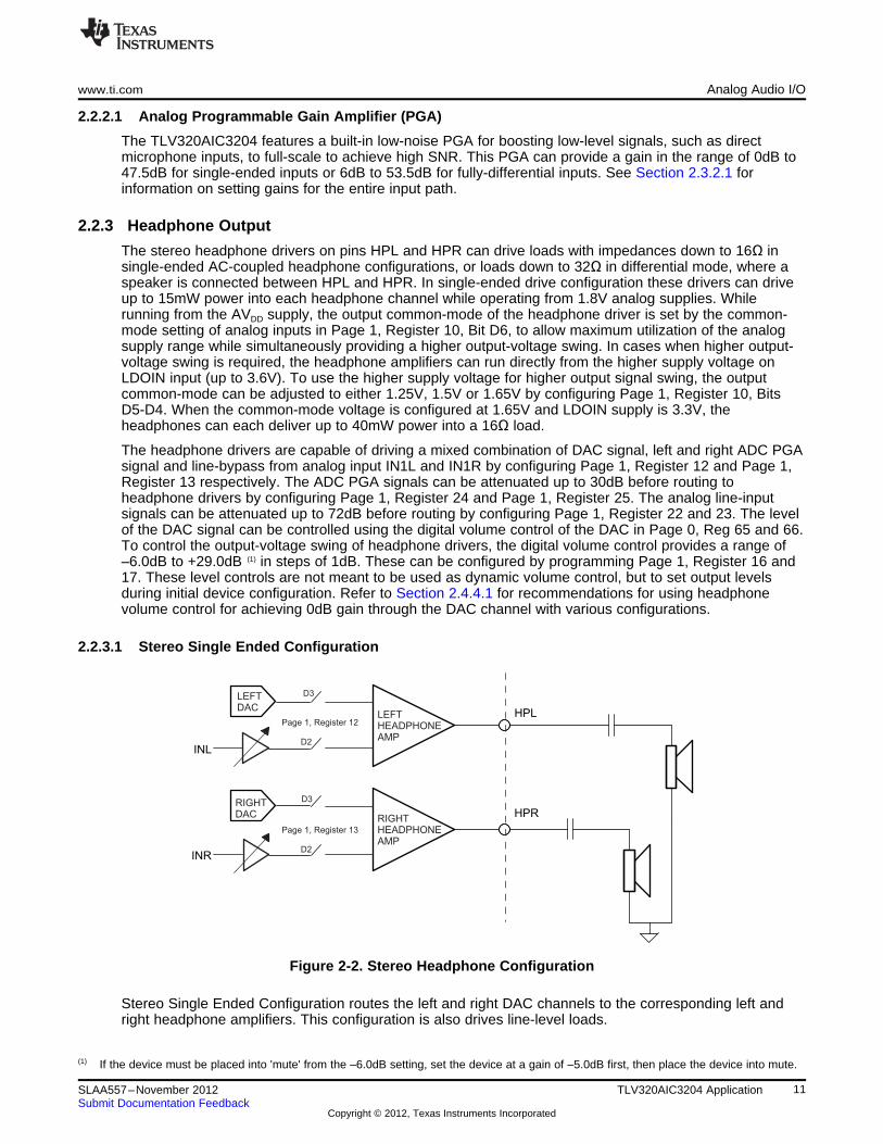
2.2.3.1 Stereo Single Ended Configuration
Figure 2-2. Stereo Headphone Configuration
Stereo Single Ended Configuration routes the left and right DAC channels to the corresponding left andright headphone amplifiers. This configuration is also drives line-level loads.
(1) If the device must be placed into 'mute' from the –6.0dB setting, set the device at a gain of –5.0dB first, then place the device into mute.
11SLAA557–November 2012 TLV320AIC3204 ApplicationSubmit Documentation Feedback
Copyright © 2012, Texas Instruments Incorporated

cmpopload
loadload V
RR
RV ´
+
=
Rload
Rpop
CcOutputDriver
PAD
Analog Audio I/O www.ti.com
The TLV320AIC3204 headphone drivers support pop-free operation. Because the HPL and HPR are high-power drivers, pop can result due to sudden transient changes in the output drivers if not prevented bycareful design. The most critical care is required while using the drivers as stereo single-endedcapacitively-coupled drivers as shown in Figure 2-2. The output drivers achieve pop-free power-up byusing slow power-up modes. Conceptually, the circuit during power-up can be visualized as
Figure 2-3. Conceptual Circuit for Pop-Free Power-up
The value of Rpop can be chosen by setting register Page 1, Register 20, D(1:0).
Table 2-3. Rpop Values
Page 1, Register 20, D(1:0) Rpop Value
00 2kΩ01 6kΩ10 25kΩ
To minimize audible artifacts, two parameters can be adjusted to match application requirements. Thevoltage Vload across Rload at the beginning of slow charging should not be more than a few mV. At that timethe voltage across Rload can be determined as:
(1)
For a typical Rload of 32Ω, an Rpop of 6kΩ or 25kΩ delivers good results (see Table 2-3 for registersettings).
According to the conceptual circuit in Figure 2-3, the voltage on PAD exponentially settles to the outputcommon-mode voltage based on the value of Rpop and Cc. Thus, the output drivers must remain in slowpower-up mode for time T, such that at the end of the slow power-on period, the voltage on Vpad is veryclose to the common-mode voltage. The TLV320AIC3204 allows adjusting the time T to allow for a widerange of Rload and Cc by programming Page 1, Register 20, D(5:2). For the time adjustments, the typicalvalue of Cc is 47μF. N = 5 generally yields good results.
Page 1, Register 20, D(5:2) Slow Charging Time = N * Time – Constants (for Rpop and47μF)
0000 N = 0
0001 N = 0.5
0010 N = 0.625
0011 N = 0.75
0100 N = 0.875
0101 N = 1.0
0110 N = 2.0
0111 N = 3.0
1000 N = 4.0
1001 N = 5.0
1010 N = 6.0
1011 N = 7.0
12 TLV320AIC3204 Application SLAA557–November 2012Submit Documentation Feedback
Copyright © 2012, Texas Instruments Incorporated

www.ti.com Analog Audio I/O
Page 1, Register 20, D(5:2) Slow Charging Time = N * Time – Constants (for Rpop and47μF)
1100 N = 8.0
1101 N = 16 (Not valid for Rpop = 25kΩ)
1110 N = 24 (Not valid for Rpop = 25kΩ)
1111 N = 32 (Not valid for Rpop = 25kΩ)
Again, for example, for Rload = 32Ω, Cc = 47μF and common mode of 0.9V, the number of time constantsrequired for pop-free operation is 5 or 6. A higher or lower Cc value will require higher or lower value for N.
During the slow-charging period, no signal is routed to the output driver. Therefore, choosing a larger thannecessary value of N results in a delay from power-up to signal at output. At the same time, choosing N tobe smaller than the optimal value results in poor pop performance at power-up.
The signals that are routed to headphone drivers (for example, DAC, MAL , MAR and IN1) often have DCoffsets due to less-than-ideal processing. As a result, when these signals are switched on to outputdrivers, the offset voltage causes a pop. To reduce audible pop in such situations, a feature is provided tosoft-step the DC-offset. At the beginning of the signal route change, a high-value attenuation can beapplied and progressively stepped lower until the desired gain in the channel is reached. Page 1, Register20, D(7:6) control the time interval between each of these gain changes. This gain soft-stepping only actsduring the initial routing of the signal to the output driver and not during subsequent gain changes.
Page 1, Register 20, D(7:6) Soft-stepping Step Time During initial signal routing
00 0 ms (soft-stepping disabled)
01 50ms
10 100ms
11 200ms
TI recommends the following sequence for achieving optimal pop performance at power-up:
1. Choose the value of Rpop, N (time constants) and soft-stepping step time for slow power-up.
2. Choose the configuration for output drivers, including common modes and output stage powerconnections
3. Select the signals to be routed to headphones.
4. Power-up the blocks driving signals into HPL and HPR, but keep the blocks muted
5. Unmute HPL and HPR and set the desired gain setting.
6. Power-on the HPL and HPR drivers.
7. Unmute the block driving signals to HPL and HPR after the Driver PGA flags are set to indicatecompletion of soft-stepping after power-up. Read these flags from Page 1, Register 63, D(7:6).
It is important to configure the Headphone Output driver depop control registers before powering up theheadphone; do not change these register contents while the headphone drivers are powered up.
Before powering down the HPL and HPR drivers, TI recommends that the user read back the flags inPage 1, Register 63. For example, before powering down the HPL driver, ensure that bit D(7) = 1 and bitD(3) = 1 if IN1L is routed to HPL and bit D(1) = 1 if the Left Mixer is routed to HPL. Power down the outputdriver only after a steady-state power-up condition has been achieved. This steady-state power-upcondition also must be satisfied for changing the HPL and HPR driver mute controls in Page 1, Register16 and 17, D(7); mute or unmute after the gain and volume controls associated with routing to HPL andHPR finish soft-stepping.
In the differential configuration of HPL and HPR, when no coupling capacitor is used, the slow chargingmethod for pop-free performance is unnecessary. In the differential load configuration for HPL and HPR,the output driver MUTE feature may cause a pop, and is not recommended.
During the power-down state, the headphone outputs are weakly pulled to ground using an approximately50kΩ resistor to ground, to maintain the output voltage on HPL and HPR pins.
13SLAA557–November 2012 TLV320AIC3204 ApplicationSubmit Documentation Feedback
Copyright © 2012, Texas Instruments Incorporated

HPL
HPR
LEFT
DAC
HPL
HPR
LEFT_DACP
LEFT_DACM
Analog Audio I/O www.ti.com
2.2.3.2 Mono Differential DAC to Mono Differential Headphone Output
Figure 2-4. Low Power Mono DAC to Differential Headphone
This configuration routes the two differential outputs of the mono, left channel DAC to the headphoneamplifiers in differential mode (Page 1, Register 12, D(3) = 1 and Page 1, Register 13, D(4) = 1).
2.2.3.3 Mono DAC and Analog Bypass Input to Mono Differential Headphone Output
Figure 2-5. Mono DAC and Analog Bypass Input to Mono Differential Headphone Output
This configuration routes a single ended signal from the mono, left channel DAC output to the headphoneamplifiers. The headphone amplifiers create a differential output form the single ended input (Page 1,Register 13, D(0) = 1). In addition, the mono analog bypass signal from INL can be mixed to the DACoutput signal (Page 1, Register 12, D(2) = 1). To use this configuration, power the headphone amplifierfrom AVDD, and set the common mode voltage to the full-chip common mode voltage (Page 1, Register 10,D(5) = 0, D(4) = 0, D(1) = 0).
2.2.3.4 Headphone Amplifier Class-D Mode
By default the headphone amplifiers in the TLV320AIC3204 work in Class-AB mode. By writing to Page 1,Register 3, D(7:6) for the left headphone amplifier, and Page 1, Register 4, D(7:6) with value 11, theheadphone amplifiers enter a Class-D mode of operation.
In this mode a high frequency digital pulse-train representation of the DAC signal is fed to the loadconnected to HPL and HPR outputs.
Because the output signal is a pulse train switching between Power Supply and Ground, the efficiency ofthe amplifier is greatly improved. This mode however, requires a clean analog power supply for goodnoise performance.
Class-D mode operation requires the following clock-divider condition:
MDAC = I × 4, where I = 1, 2, ..., 32
14 TLV320AIC3204 Application SLAA557–November 2012Submit Documentation Feedback
Copyright © 2012, Texas Instruments Incorporated

HPL
HPR
L = 82 Hm C = 47 FC
m
C = 1 FmRload = 32 W
www.ti.com Analog Audio I/O
When a direct digital pulse train is driven out as a signal, high frequencies as a function of pulse trainfrequency are also present which waste power. Use an LC filter in series with the output and the load toincrease the efficiency and reduce power dissipation in the load due to these high frequencies. Adjust thecutoff frequency of the LC filter to allow audio signals below 20kHz to pass through, but highly attenuatethe high-frequency signal content.
Figure 2-6. Configuration for Using Headphone Amplifier in Class-D Mode
To use the headphone amplifiers in Class-D mode, first power up the headphone amplifiers in the defaultClass-AB mode to charge the AC-coupling capacitor to the set common mode voltage. After theheadphone amplifiers power up, route the DAC to the headphone amplifiers and unmute them before theycan switch to Class-D mode. After Class D mode turns on, the linear Class AB mode amplifier must beturned off. Mute the DAC before powering down the headphone amplifiers.
See Section 4.0.3 for an example setup script enabling Class-D mode.
Differential LoadingThe headphone amplifiers can be configured differentially as shown in Figure 2-7. However, this schemeis supported only when using the headphone-output stage powered from the AVDD supply.
Figure 2-7. Differential Receiver Speaker Configuration
2.2.4 Line Outputs
The stereo line level drivers on LOL and LOR pins can drive a wide range of line level resistiveimpedances in the range of 600Ω to 10kΩ. The output common modes of line level drivers can beconfigured to equal either the analog input common-mode setting or to 1.65V. With output common-modesetting of 1.65V and DRVdd_HP supply at 3.3V the line-level drivers can drive up to 1Vrms output signal.The line-level drivers can drive out a mixed combination of DAC signal and attenuated ADC PGA signal.Signal mixing is register-programmable.
2.2.4.1 Line Out Amplifier Configurations
Signal mixing can be configured by programming Page 1, Register 14 and 15. Additionally, the two line-level drivers can be configured to act as a mono differential line level driver by routing the output of LORto LOL (Page 1, Register 14, D(0) = 1).
The output of DAC can be simultaneously played back to the stereo headphone drivers as well as stereoline- level drivers. In such a case, the DAC signal at the headphone outputs and line outputs are out-of-phase with respect to each other.
15SLAA557–November 2012 TLV320AIC3204 ApplicationSubmit Documentation Feedback
Copyright © 2012, Texas Instruments Incorporated

RIGHT
DAC AFIR
Output +
LOR
RIGHT_DACP
RIGHT_DACM
LOL
Output -
LOL
LOR
ADC www.ti.com
Figure 2-8. Stereo Single-Ended Line-out
Figure 2-9. Low Power Mono DAC to Differential Line-out
2.3 ADC
The TLV320AIC3204 includes a stereo audio ADC, which uses a delta-sigma modulator with aprogrammable oversampling ratio, followed by a digital decimation filter. The ADC supports sampling ratesfrom 8kHz to 192kHz. In order to provide optimal system power management, the stereo recording pathcan be powered up one channel at a time, to support the case where only mono record capability isrequired.
The ADC path of the TLV320AIC3204 features a large set of options for signal conditioning as well assignal routing:
• Two ADCs
• Six analog inputs which can be mixed and-or multiplexed in single-ended and-or differentialconfiguration
• Two programmable gain amplifiers (PGA) with a range of 0 to +47.5dB
• Two mixer amplifiers for analog bypass
• Two low power analog bypass channels
• Fine gain adjustment of digital channels with 0.1dB step size
• Digital volume control with a range of -12 to +20dB
• Mute function
• Automatic gain control (AGC)
In addition to the standard set of ADC features the TLV320AIC3204 also offers the following specialfunctions:
16 TLV320AIC3204 Application SLAA557–November 2012Submit Documentation Feedback
Copyright © 2012, Texas Instruments Incorporated
AnalogGain
AnalogIn
InputSelection
ADCFiltering
DigitalVolumeControl
DigitalGain
Adjust
0...47.5 dBStep = 0.5 dB
0, -6, -12 dB -12...20 dBStep = 0.5 dB
0…-0.4 dBStep= 0.1 dB
FrequencyResponseand Gain
FullyProgrammable
Coefficients
AudioInterface
ADC
PGA
www.ti.com ADC
• Built in microphone bias
• Stereo digital microphone interface
• Channel-to-channel phase adjustment
• Fast charge of ac-coupling capacitors
• Anti thump
• Adaptive filter mode
Because of the oversampling nature of the audio ADC and the integrated digital decimation filtering,requirements for analog anti-aliasing filtering are very relaxed. The TLV320AIC3204 integrates a secondorder analog anti-aliasing filter with 28-dB attenuation at 6MHz. This filter, combined with the digitaldecimation filter, provides sufficient anti-aliasing filtering without requiring additional external components.
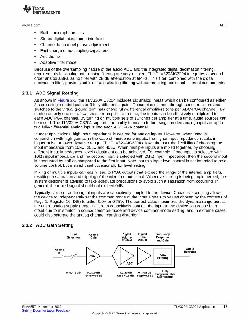
2.3.1 ADC Signal Routing
As shown in Figure 2-1, the TLV320AIC3204 includes six analog inputs which can be configured as either3 stereo single-ended pairs or 3 fully-differential pairs. These pins connect through series resistors andswitches to the virtual ground terminals of two fully-differential amplifiers (one per ADC-PGA channel). Byturning on only one set of switches per amplifier at a time, the inputs can be effectively multiplexed toeach ADC PGA channel. By turning on multiple sets of switches per amplifier at a time, audio sources canbe mixed. The TLV320AIC3204 supports the ability to mix up to four single-ended analog inputs or up totwo fully-differential analog inputs into each ADC PGA channel.
In most applications, high input impedance is desired for analog inputs. However, when used inconjunction with high gain as in the case of microphone inputs, the higher input impedance results inhigher noise or lower dynamic range. The TLV320AIC3204 allows the user the flexibility of choosing theinput impedance from 10kΩ, 20kΩ and 40kΩ. When multiple inputs are mixed together, by choosingdifferent input impedances, level adjustment can be achieved. For example, if one input is selected with10kΩ input impedance and the second input is selected with 20kΩ input impedance, then the second inputis attenuated by half as compared to the first input. Note that this input level control is not intended to be avolume control, but instead used occasionally for level setting.
Mixing of multiple inputs can easily lead to PGA outputs that exceed the range of the internal amplifiers,resulting in saturation and clipping of the mixed output signal. Whenever mixing is being implemented, thesystem designer is advised to take adequate precautions to avoid such a saturation from occurring. Ingeneral, the mixed signal should not exceed 0dB.
Typically, voice or audio signal inputs are capacitively coupled to the device. Capacitive coupling allowsthe device to independently set the common mode of the input signals to values chosen by the contents ofPage 1, Register 10, D(6) to either 0.9V or 0.75V. The correct value maximizes the dynamic range acrossthe entire analog-supply range. Failure to capacitively connect the input to the device can cause highoffset due to mismatch in source common-mode and device common-mode setting, and in extreme cases,could also saturate the analog channel, causing distortion.
2.3.2 ADC Gain Setting
17SLAA557–November 2012 TLV320AIC3204 ApplicationSubmit Documentation Feedback
Copyright © 2012, Texas Instruments Incorporated

ADC www.ti.com
When the gain of the ADC Channel is kept at 0dB and the common mode set to 0.75V, a single-endedinput of 0.375VRMS results in a full-scale digital signal at the output of ADC channel. Similarly, when thegain is kept at 0dB, and common mode is set to 0.9V, a single-ended input of 0.5VRMS results in a full-scale digital signal at the output of the ADC channel. However various block functions control the gainthrough the channel. The gain applied by the PGA is described in Table 2-4. Additionally, the digitalvolume control adjusts the gain through the channel as described in Section 2.3.2.2. A finer level of gain iscontrolled by fine gain control as described in Section 2.3.2.2.1. The decimation filters A, B and C alongwith the delta-sigma modulator contribute to a DC gain of 1.0 through the channel.
2.3.2.1 Analog Programmable Gain Amplifier (PGA)
The TLV320AIC3204 features a built-in low-noise PGA for boosting low-level signals, such as directmicrophone inputs, to full-scale to achieve high SNR. This PGA provides a gain in the range of 0dB to47.5dB for single-ended inputs or 6dB to 53.5dB for fully-differential inputs (gain calculated w.r.t. inputimpedance setting of 10kΩ, 20kΩ input impedance will result in 6dB lower and 40kΩ will result in 12dBlower gain). The user can control the gain by writing to Page 1, Register 59 and Page 1, Register 60. Inthe AGC mode, this gain is optionally automatically controlled by the built-in hardware AGC.
Table 2-4. Analog PGA versus Input Configuration
Page 1, EFFECTIVE GAIN APPLIED BY PGARegister 59, D(6:0) SINGLE-ENDED DIFFERENTIALPage 1,
RIN = 10kΩ RIN = 20kΩ RIN = 40kΩ RIN = 10kΩ RIN = 20kΩ RIN = 40kΩRegister 60, D(6:0)
000 0000 0dB –6dB -12dB 6.0dB 0dB –6.0dB
000 0001 0.5dB –5.5dB –11.5dB 6.5dB 0.5dB -5.5dB
000 0010 1.0dB –5.0dB –11.0dB 7.0dB 7.5dB –5.0dB
… … … … … … …
101 1110 47.0dB 41.0dB 35.0dB 53.0dB 47.0dB 41.0dB
101 1111 47.5dB 41.5dB 35.5dB 53.5dB 47.5dB 41.5dB
The gain changes are implemented with an internal soft-stepping algorithm that only changes the actualvolume level by one 0.5dB step every one or two ADC output samples, depending on the register value(see registers Page 0, Reg 81, D(1:0)). This soft-stepping smooths volume control changes with noaudible artifacts. On reset, the PGA gain defaults to a mute condition, and at power down, the PGA soft-steps the volume to mute before shutting down. A read-only flag Page 0, Reg 36, D(7) and D(3) is setwhenever the gain applied by the PGA equals the desired value set by the register. The soft-steppingcontrol can also be disabled by programming Page 0, Reg 81, D(1:0).
2.3.2.2 Digital Volume Control
The TLV320AIC3204 also has a digital volume-control block with a range from -12dB to +20dB in steps of0.5dB. The system controls the volume by programming Page 0, Register 83 and 84 respectively for leftand right channels.
Table 2-5. Digital Volume Control for ADC
Desired Gain Left or Right ChanneldB Page 1, Register 83 or 84 (respectively),
D(6:0)
–12.0 110 1000
–11.5 110 1001
–11.0 110 1010
..
–0.5 111 1111
0.0 000 0000 (Default)
+0.5 000 0001
..
18 TLV320AIC3204 Application SLAA557–November 2012Submit Documentation Feedback
Copyright © 2012, Texas Instruments Incorporated
www.ti.com ADC
Table 2-5. Digital Volume Control for ADC (continued)
Desired Gain Left or Right ChanneldB Page 1, Register 83 or 84 (respectively),
D(6:0)
+19.5 010 0111
+20.0 010 1000
During volume control changes, using the soft-stepping feature avoids audible artifacts. The soft-steppingrate can be set to either 1 or 2 gain steps per sample. Soft-stepping can also be entirely disabled. Thissoft-stepping is configured via Page 1, Register 81, D(1:0), and is common to the soft-stepping control forthe analog PGA. During power-down of an ADC channel, this volume control soft-steps down to –12.0dBbefore powering down. Due to the soft-stepping control, soon after changing the volume control setting orpowering down the ADC channel, the actual applied gain may be different from the one programmedthrough the control register. The TLV320AIC3204 gives feedback to the user, through read-only flagsPage 1, Reg 36, D(7) for Left Channel and Page 1, Reg 36, D(3) for the right channel.
2.3.2.2.1 Fine Digital Gain Adjustment
Additionally, the gain in each of the channels is finely adjustable in steps of 0.1dB. This granularity isuseful when trying to match the gain between channels. By programming Page 0, Register 82 the gaincan be adjusted from 0dB to -0.4dB in steps of 0.1dB. This feature, in combination with the regular digitalvolume control, allows the gains through the left and right channels be matched in the range of -0.5dB to+0.5dB with a resolution of 0.1dB.
2.3.2.3 AGC
The TLV320AIC3204 includes Automatic Gain Control (AGC) for ADC recording. AGC can be used tomaintain a nominally-constant output level when recording speech. As opposed to manually setting thePGA gain, in the AGC mode, the circuitry automatically adjusts the PGA gain as the input signal becomesoverly loud or very weak, such as when a person speaking into a microphone moves closer or farther fromthe microphone. The AGC algorithm has several programmable parameters, including target gain, attackand decay time constants, noise threshold, and max PGA applicable, that allow the algorithm to be finetuned for any particular application. The algorithm uses the absolute average of the signal (which is theaverage of the absolute value of the signal) as a measure of the nominal amplitude of the output signal.Since the gain can be changed at the sample interval time, the AGC algorithm operates at the ADCsample rate.
1. Target Level represents the nominal output level at which the AGC attempts to hold the ADC outputsignal level. The TLV320AIC3204 allows programming of eight different target levels, which can beprogrammed from –5.5dB to –24dB relative to a full-scale signal. Since the TLV320AIC3204 reacts tothe signal absolute average and not to peak levels, it is recommended that the target level be set withenough margin to avoid clipping at the occurrence of loud sounds.
2. Attack Time defines how quickly the AGC circuitry reduces the PGA gain when the output signal levelexceeds the target level due to increase in input signal level. Wide range of attack timeprogrammability is supported in terms of number of samples (number of ADC sample frequency clockcycles).
3. Decay Time defines how quickly the PGA gain is increased when the output signal level falls belowthe target level due to reduction in input signal level. Wide range of decay time programmability issupported in terms of number of samples.
4. Gain Hysteresis is the hysteresis applied to the required gain calculated by the AGC function whilechanging its mode of operation from attack to decay or vice-versa. For example, while attacking theinput signal, if the current applied gain by the AGC is xdB, and suddenly because of the input levelgoing down, the new calculated required gain is ydB, then this gain is applied, provided that y isgreater than x by the value set in Gain Hysteresis. This feature avoids the condition where the AGCfunction fluctuates between a very narrow band of gains leading to audible artifacts. The GainHysteresis can be adjusted or disabled by the user.
5. Noise threshold defines the level below which if the input signal level falls, the AGC considers it assilence, and thus brings down the gain to 0dB in steps of 0.5dB every fS and sets the noise threshold
19SLAA557–November 2012 TLV320AIC3204 ApplicationSubmit Documentation Feedback
Copyright © 2012, Texas Instruments Incorporated

11
23
110
zD2
zNN)z(H
-
-
-
+
=
ADC www.ti.com
flag. The gain stays at 0dB unless the input speech signal average rises above the noise thresholdsetting. This noise-gating ensures that noise is not 'gained up' in the absence of speech. Noisethreshold level in the AGC algorithm is programmable from -30dB to -90dB of full-scale. When AGCNoise Threshold is set to –70dB, –80dB, or –90dB, the microphone input Max PGA applicable settingmust be greater than or equal to 11.5dB, 21.5dB, or 31.5dB respectively. This operation includeshysteresis and debounce to avoid the AGC gain from cycling between high gain and 0dB when signalsare near the noise threshold level. The noise (or silence) detection feature can be entirely disabled bythe user.
6. Max PGA applicable allows the designer to restrict the maximum gain applied by the AGC. Thisfeature limits PGA gain in situations where environmental noise is greater than the programmed noisethreshold. Microphone input Max PGA is programmable from 0dB to 58dB in steps of 0.5dB.
7. Hysteresis, as the name suggests, defines a window around the Noise Threshold which must beexceeded to either detect that the recorded signal is indeed noise or signal. If initially the energy of therecorded signal is greater than the Noise Threshold, then the AGC recognizes it as noise only whenthe energy of the recorded signal falls below the Noise Threshold by a value given by Hysteresis.Similarly, after the recorded signal is recognized as noise, for the AGC to recognize it as a signal, itsenergy must exceed the Noise Threshold by a value given by the Hysteresis setting. In order toprevent the AGC from jumping between noise and signal states, (which can happen when the energyof recorded signal is very close to the Noise threshold) a non-zero hysteresis value should be chosen.The Hysteresis feature can also be disabled.
8. Debounce Time (Noise and Signal) defines the hysteresis in time domain for noise detection. TheAGC continuously calculates the energy of the recorded signal. If the calculated energy is less than theset Noise Threshold, then the AGC does not increase the input gain to achieve the Target Level.However, to handle audible artifacts which can occur when the energy of the input signal is very closeto the Noise Threshold, the AGC checks if the energy of the recorded signal is less than the NoiseThreshold for a time greater than the Noise Debounce Time. Similarly the AGC starts increasing theinput-signal gain to reach the Target Level when the calculated energy of the input signal is greaterthan the Noise Threshold. Again, to avoid audible artifacts when the input-signal energy is very closeto Noise Threshold, the energy of the input signal needs to continuously exceed the Noise Thresholdvalue for the Signal Debounce Time. If the debounce times are kept very small, then audible artifactscan result by rapid enabling and disabling the AGC function. At the same time, if the Debounce time iskept too large, then the AGC may take time to respond to changes in levels of input signals withrespect to Noise Threshold. Both noise and signal debounce time can be disabled.
9. The AGC Noise Threshold Flag is a read-only flag indicating that the input signal has levels lowerthan the Noise Threshold, and thus is detected as noise (or silence). In such a condition the AGCapplies a gain of 0dB.
10. Gain Applied by AGC is the gain applied by the AGC to the recorded signal in a read-only register toprovide real-time feedback to the system. This value, along with the Target Setting, can be used todetect the input signal level. In a steady state situationTarget Level (dB ) = Gain Applied by AGC (dB) + Input Signal Level (dB)When the AGC noise threshold flag is set, then the status of gain applied by AGC should be ignored.
11. The AGC Saturation Flag is a read-only flag indicating that the ADC output signal has not reached itsTarget Level. However, the AGC is unable to increase the gain further because the required gain ishigher than the Maximum Allowed PGA gain. Such a situation can happen when the input signal hasvery low energy and the Noise Threshold is also set very low. When the AGC noise threshold flag isset, the status of the AGC saturation flag should be ignored.
12. The ADC Saturation Flag is a read-only flag indicating an overflow condition in the ADC channel. Onoverflow, the signal is clipped and distortion results. This condition typically happens when the AGCTarget Level is kept very high and the energy in the input signal increases faster than the Attack Time.
13. An AGC low-pass filter detects the average level of the input signal. This average level is comparedto the programmed detection levels in the AGC to provide the correct functionality. This low pass filteris in the form of a first-order IIR filter. Three 8-bit registers form the 24-bit digital coefficient as shownon the register map. A total of 9 registers are programmed to form the 3 IIR coefficients. The transferfunction of the filter implemented for signal level detection is given by
(2)
20 TLV320AIC3204 Application SLAA557–November 2012Submit Documentation Feedback
Copyright © 2012, Texas Instruments Incorporated

Decay Time
Target
Level
Input
Signal
Output
Signal
AGC
Gain
AttackTime
www.ti.com ADC
Where:Coefficient N0 can be programmed by writing into Page 8, Register 12, 13 and 14.Coefficient N1 can be programmed by writing into Page 8, Register 16, 17 and 18.Coefficient D1 can be programmed by writing into Page 8, Register 20, 21 and 22.N0, N1 and D1 are 24-bit 2’s complement numbers and their default values implement a low-passfilter with cut-off at 0.002735*ADC_FS.
See Table 2-6 for various AGC programming options. AGC can be used only if analog microphoneinput is routed to the ADC channel.
Table 2-6. AGC Parameter Settings
Function Control Register Control Register BitLeft ADC Right ADC
AGC enable Page 0, Register 86 Page 0,Register 94 D(7)
Target Level Page 0, Register 86 Page 0, Register 94 D(6:4)
Gain Hysteresis Page 0, Register 86 Page 0, Register 94 D(1:0)
Hysteresis Page 0, Register 87 Page 0, Register 95 D(7:6)
Noise threshold Page 0, Register 87 Page 0, Register 95 D(5:1)
Max PGA applicable Page 0, Register 88 Page 0, Register 96 D(6:0)
Time constants (attack time) Page 0, Register 89 Page 0, Register 97 D(7:0)
Time constants(decay time) Page 0, Register 90 Page 0, Register 98 D(7:0)
Debounce time (Noise) Page 0, Register 91 Page 0, Register 99 D(4:0)
Debounce time (Signal) Page 0, Register 92 Page 0, Register 100 D(3:0)
Gain applied by AGC Page 0, Register 93 Page 0, Register 101 D(7:0) (Read Only)
AGC Noise Threshold Flag Page 0, Register 45 (sticky flag), Page 0, Register 45 (sticky flag), D(6:5) (Read Only)Page 0, Register 47 (non-sticky Page 0, Register 47 (non-stickyflag) flag)
AGC Saturation flag Page 0, Register 36 (sticky flag) Page 0, Register 36 (sticky flag) D(5), D(1) (Read Only)
ADC Saturation flag Page 0, Register 42 (sticky flag), Page 0, Register 42 (sticky flag), D(3:2) (Read Only)Page 0, Register 43 (non-sticky Page 0, Register 43 (non-stickyflag) flag)
Figure 2-10. AGC Characteristics
21SLAA557–November 2012 TLV320AIC3204 ApplicationSubmit Documentation Feedback
Copyright © 2012, Texas Instruments Incorporated

ADC www.ti.com
2.3.3 ADC Decimation Filtering and Signal Processing Overview
The TLV320AIC3204 ADC channel includes a built-in digital decimation filter to process the oversampleddata from the sigma-delta modulator to generate digital data at Nyquist sampling rate with high dynamicrange. The decimation filter can be chosen from three different types, depending on the requiredfrequency response, group delay and sampling rate.
ADC Processing Blocks
The TLV320AIC3204 offers a range of processing blocks which implement various signal processingcapabilities along with decimation filtering. These processing blocks give users the choice of how muchand what type of signal processing they may use and which decimation filter is applied.
The choice between these processing blocks is part of the PowerTune strategy to balance powerconservation and signal-processing flexibility. Less signal-processing capability reduces the powerconsumed by the device. Table 2-7 gives an overview of the available processing blocks and theirproperties. The Resource Class Column (RC) gives an approximate indication of power consumption.
The signal processing blocks available are:
• First-order IIR
• Scalable number of biquad filters
• Variable-tap FIR filter
• AGC
The processing blocks are tuned for common cases and can achieve high anti-alias filtering or low groupdelay in combination with various signal processing effects such as audio effects and frequency shaping.The available first order IIR, BiQuad and FIR filters have fully user-programmable coefficients. TheResource Class Column (RC) gives an approximate indication of power consumption.
Table 2-7. ADC Processing Blocks
Processing Channel Decimation 1st Order Number FIR Required ResourceBlocks Filter IIR BiQuads AOSR Value Class
Available
PRB_R1 (1) Stereo A Yes 0 No 128,64 6
PRB_R2 Stereo A Yes 5 No 128,64 8
PRB_R3 Stereo A Yes 0 25-Tap 128,64 8
PRB_R4 Right A Yes 0 No 128,64 3
PRB_R5 Right A Yes 5 No 128,64 4
PRB_R6 Right A Yes 0 25-Tap 128,64 4
PRB_R7 Stereo B Yes 0 No 64 3
PRB_R8 Stereo B Yes 3 No 64 4
PRB_R9 Stereo B Yes 0 20-Tap 64 4
PRB_R10 Right B Yes 0 No 64 2
PRB_R11 Right B Yes 3 No 64 2
PRB_R12 Right B Yes 0 20-Tap 64 2
PRB_R13 Stereo C Yes 0 No 32 3
PRB_R14 Stereo C Yes 5 No 32 4
PRB_R15 Stereo C Yes 0 25-Tap 32 4
PRB_R16 Right C Yes 0 No 32 2
PRB_R17 Right C Yes 5 No 32 2
PRB_R18 Right C Yes 0 25-Tap 32 2(1) Default
22 TLV320AIC3204 Application SLAA557–November 2012Submit Documentation Feedback
Copyright © 2012, Texas Instruments Incorporated

To AudioInterface
1st
OrderIIR
AGCGain
Compen-
sation
AGC
Filter B
To AudioInterface
To Analog PGA
From Delta-SigmaModulator ´
From Digital Vol. Ctrl
1st
OrderIIR
AGCGain
Compen-
sation
AGC
Filter A 25-Tap FIRFrom Delta-Sigma
Modulator
To Analog PGA
To Audio
Interface´
From Digital Vol. Ctrl
1st
OrderIIR
AGCGain
Compen-sation
AGC
Filter A H EH DH CHBH ATo Audio
Interface
To Analog PGA
From Delta-SigmaModulator ´
From Digital Vol. Ctrl
To AudioInterface
1st
OrderIIR´
AGCGain
Compen-sation
AGC
To Analog PGA
Filter AFrom Delta-Sigma
Modulator
From Digital Vol. Ctrl
www.ti.com ADC
2.3.3.1 Signal Processing Blocks – Details
2.3.3.1.1 First-Order IIR, AGC, Filter A
Figure 2-11. Signal Chain for PRB_R1 and PRB_R4
2.3.3.1.2 5 Biquads, First-Order IIR, AGC, Filter A
Figure 2-12. Signal Chain PRB_R2 and PRB_R5
2.3.3.1.3 25 Tap FIR, First-Order IIR, AGC, Filter A
Figure 2-13. Signal Chain for PRB_R3 and PRB_R6
2.3.3.1.4 First-Order IIR, AGC, Filter B
Figure 2-14. Signal Chain for PRB_R7 and PRB_R10
23SLAA557–November 2012 TLV320AIC3204 ApplicationSubmit Documentation Feedback
Copyright © 2012, Texas Instruments Incorporated
1st
OrderIIR
AGCGain
Compen-sation
AGC
Filter C H EH DH CHBH AFrom Delta-Sigma
Modulator
From Digital Vol. Ctrl
To Analog PGA
To Audio
Interface´
1st
OrderIIR
AGCGain
Compen-
sation
AGC
Filter CFrom Delta-Sigma
Modulator
From Digital Vol. Ctrl
To Analog PGA
To AudioInterface
´
1st
OrderIIR
AGCGain
Compen-
sation
AGC
Filter B 20-Tap FIRFrom Delta-Sigma
Modulator
To Analog PGA
To Audio
Interface´
From Digital Vol. Ctrl
1st
OrderIIR
AGCGain
Compen-sation
AGC
Filter B HCHBHAFrom Delta-Sigma
Modulator
To Analog PGA
To Audio
Interface´
From Digital Vol. Ctrl
ADC www.ti.com
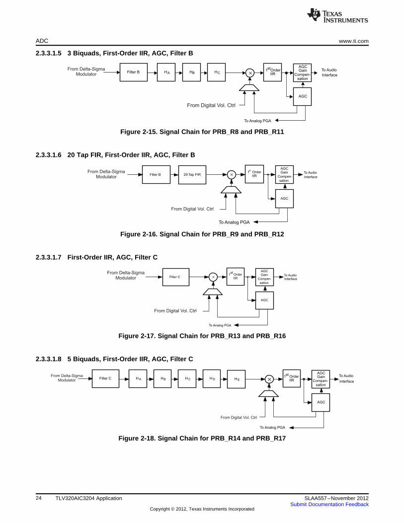
2.3.3.1.5 3 Biquads, First-Order IIR, AGC, Filter B
Figure 2-15. Signal Chain for PRB_R8 and PRB_R11
2.3.3.1.6 20 Tap FIR, First-Order IIR, AGC, Filter B
Figure 2-16. Signal Chain for PRB_R9 and PRB_R12
2.3.3.1.7 First-Order IIR, AGC, Filter C
Figure 2-17. Signal Chain for PRB_R13 and PRB_R16
2.3.3.1.8 5 Biquads, First-Order IIR, AGC, Filter C
Figure 2-18. Signal Chain for PRB_R14 and PRB_R17
24 TLV320AIC3204 Application SLAA557–November 2012Submit Documentation Feedback
Copyright © 2012, Texas Instruments Incorporated

11
23
110
zD2
zNN)z(H
-
-
-
+
=
1st
OrderIIR
AGCGain
Compen
sation
AGC
Filter C 25-Tap FIRFrom Delta-Sigma
Modulator
From Digital Vol. Ctrl
To Analog PGA
To Audio
Interface´
www.ti.com ADC
2.3.3.1.9 25 Tap FIR, First-Order IIR, AGC, Filter C
Figure 2-19. Signal for PRB_R15 and PRB_R18
2.3.3.1.10 User Programmable Filters
Depending on the selected processing block, different types and orders of digital filtering are available. Afirst order IIR filter is always available, and is useful to efficiently filter out possible DC components of thesignal. Up to 5 biquad sections, or alternatively up to 25-tap FIR filters are available for specific processingblocks. The coefficients of the available filters are arranged as sequentially indexed coefficients in twobanks. If adaptive filtering is chosen, the coefficient banks can be switched during operation withoutdisruption. For more details on adaptive filtering see Section 2.3.3.2.7 below.
The coefficients of these filters are each 24-bits wide, in two's-complement and occupy 3 consecutive 8-bitregisters in the register space. For default values please see Section 5.11.
2.3.3.1.10.1 First-Order IIR Section
The transfer function for the first order IIR Filter is given by
(3)
The frequency response for the first-order IIR Section with default coefficients is flat at a gain of 0dB.Details on ADC coefficient default values are given in Section 5.11.
Table 2-8. ADC 1st order IIR Filter Coefficients
Filter FIlter ADC Coefficient Left ADC Coefficient Right ChannelCoefficient Channel
N0 C4 (Pg 8,Reg 24,25,26) C36 (Pg 9,Reg 32,33,34)First Order N1 C5 (Pg 8,Reg 28,29,30) C37 (Pg 9,Reg 36,37,38)IIR
D1 C6 (Pg 8,Reg 32,33,34) C39 (Pg 9,Reg 40,41,42)
25SLAA557–November 2012 TLV320AIC3204 ApplicationSubmit Documentation Feedback
Copyright © 2012, Texas Instruments Incorporated

22
11
23
22
110
zDzD*22
zNzN*2N)z(H
--
--
--
++
=
ADC www.ti.com
2.3.3.1.10.2 Biquad Section
The transfer function of each of the Biquad Filters is given by
(4)
The frequency response for each of the biquad section with default coefficients is flat at a gain of 0dB.Details on ADC coefficient default values are given in Section 5.11.
Table 2-9. ADC Biquad Filter Coefficients
Filter FIlter ADC Coefficient Left ADC Coefficient Right ChannelCoefficient Channel
BIQUAD A N0 C7 (Pg 8, Reg 36,37,38) C39 (Pg 9, Reg 44,45,46)
N1 C8 (Pg 8, Reg 40,41,42) C40 (Pg 9, Reg 48,49,50)
N2 C9 (Pg 8, Reg 44,45,46) C41 (Pg 9, Reg 52,53,54)
D1 C10 (Pg 8, Reg 48,49,50) C42 (Pg 9, Reg 56,57,58)
D2 C11 (Pg 8, Reg 52,53,54) C43 (Pg 9, Reg 60,61,62)
BIQUAD B N0 C12 (Pg 8, Reg 56,57,58) C44 (Pg 9, Reg 64,65,66)
N1 C13 (Pg 8, Reg 60,61,62) C45 (Pg 9, Reg 68,69,70)
N2 C14 (Pg 8, Reg 64,65,66) C46 (Pg 9, Reg 72,73,74)
D1 C15 (Pg 8, Reg 68,69,70) C47 (Pg 9, Reg 76,77,78)
D2 C16 (Pg 8, Reg 72,73,74) C48 (Pg 9, Reg 80,81,82)
BIQUAD C N0 C17 (Pg 8, Reg 76,77,78) C49 (Pg 9, Reg 84,85,86)
N1 C18 (Pg 8, Reg 80,81,82) C50 (Pg 9, Reg 88,89,90)
N2 C19 (Pg 8, Reg 84,85,86) C51 (Pg 9, Reg 92,93,94)
D1 C20 (Pg 8, Reg 88,89,90) C52 (Pg 9, Reg 96,97,98)
D2 C21 (Pg 8, Reg 92,93,94) C53 (Pg 9, Reg 100,101,102)
BIQUAD D N0 C22 (Pg 8, Reg 96,97,98) C54 (Pg 9, Reg 104,105,106)
N1 C23 (Pg 8, Reg 100,101,102) C55 (Pg 9, Reg 108,109,110)
N2 C24 (Pg 8, Reg 104,105,106) C56 (Pg 9, Reg 112,113,114)
D1 C25 (Pg 8, Reg 108,109,110) C57 (Pg 9, Reg 116,117,118)
D2 C26 (Pg 8, Reg 112,113,114) C58 (Pg 9, Reg 120,121,122)
BIQUAD E N0 C27 (Pg 8, Reg 116,117,118) C59 (Pg 9, Reg 124,125,126)
N1 C28 (Pg 8, Reg 120,121,122) C60 (Pg 10, Reg 8,9,10)
N2 C29 (Pg 8, Reg 124,125,126) C61 (Pg 10, Reg 12,13,14)
D1 C30 (Pg 9, Reg 8,9,10) C62 (Pg 10, Reg 16,17,18)
D2 C31 (Pg 9, Reg 12,13,14) C63 (Pg 10, Reg 20,21,22)
26 TLV320AIC3204 Application SLAA557–November 2012Submit Documentation Feedback
Copyright © 2012, Texas Instruments Incorporated

PRB_R12andPRB_R9for,19M
PRB_R18andPRB_R15PRB_R6,PRB_R3,for,24M
zFir)z(HM
0n
nn
=
=
= å=
-
www.ti.com ADC
2.3.3.1.10.3 FIR Section
Six of the available ADC processing blocks offer FIR filters for signal processing. PRB_R9 and PRB_R12feature a 20-tap FIR filter while the processing blocks PRB_R3, PRB_R6, PRB_R15 and PRB_R18feature a 25-tap FIR filter.
(5)
The coefficients of the FIR filters are 24-bit 2’s complement format and correspond to the ADC coefficientspace as listed below. There is no default transfer function for the FIR filter. When the FIR filter gets usedall applicable coefficients must be programmed.
Table 2-10. ADC FIR Filter Coefficients
Filter FIlter Coefficient Left ADC Filter Coefficient Right ADC ChannelChannel
Fir0 C7 (Pg 8, Reg 36,37,38) C39 (Pg 9, Reg 44,45,46)
Fir1 C8 (Pg 8, Reg 40,41,42) C40 (Pg 9, Reg 48,49,50)
Fir2 C9 (Pg 8, Reg 44,45,46) C41 (Pg 9, Reg 52,53,54)
Fir3 C10 (Pg 8, Reg 48,49,50) C42 (Pg 9, Reg 56,57,58)
Fir4 C11 (Pg 8, Reg 52,53,54) C43 (Pg 9, Reg 60,61,62)
Fir5 C12 (Pg 8, Reg 56,57,58) C44 (Pg 9, Reg 64,65,66)
Fir6 C13 (Pg 8, Reg 60,61,62) C45 (Pg 9, Reg 68,69,70)
Fir7 C14 (Pg 8, Reg 64,65,66) C46 (Pg 9, Reg 72,73,74)
Fir8 C15 (Pg 8, Reg 68,69,70) C47 (Pg 9, Reg 76,77,78)
Fir9 C16 (Pg 8, Reg 72,73,74) C48 (Pg 9, Reg 80,81,82)
Fir10 C17 (Pg 8, Reg 76,77,78) C49 (Pg 9, Reg 84,85,86)
Fir11 C18 (Pg 8, Reg 80,81,82) C50 (Pg 9, Reg 88,89,90)
Fir12 C19 (Pg 8, Reg 84,85,86) C51 (Pg 9, Reg 92,93,94)
Fir13 C20 (Pg 8, Reg 88,89,90) C52 (Pg 9, Reg 96,97,98)
Fir14 C21 (Pg 8, Reg 92,93,94) C53 (Pg 9, Reg 100,101,102)
Fir15 C22 (Pg 8, Reg 96,97,98) C54 (Pg 9, Reg 104,105,106)
Fir16 C23 (Pg 8, Reg 100,101,102) C55 (Pg 9, Reg 108,109,110)
Fir17 C24 (Pg 8, Reg 104,105,106) C56 (Pg 9, Reg 112,113,114)
Fir18 C25 (Pg 8, Reg 108,109,110) C57 (Pg 9, Reg 116,117,118)
Fir19 C26 (Pg 8, Reg 112,113,114) C58 (Pg 9, Reg 120,121,122)
Fir20 C27 (Pg 8, Reg 116,117,118) C59 (Pg 9, Reg 124,125,126)
Fir21 C28 (Pg 8, Reg 120,121,122) C60 (Pg 10, Reg 8,9,10)
Fir22 C29 (Pg 8, Reg 124,125,126) C61 (Pg 10, Reg 12,13,14)
Fir23 C30 (Pg 9, Reg 8,9,10) C62 (Pg 10, Reg 16,17,18)
Fir24 C31 (Pg 9, Reg 12,13,14) C63 (Pg 10, Reg 20,21,22)
27SLAA557–November 2012 TLV320AIC3204 ApplicationSubmit Documentation Feedback
Copyright © 2012, Texas Instruments Incorporated

0
–10
–20
–30
–40
–50
–60
–70
–80
–90
–100
0.0 0.2 0.4 0.6 0.8 1.0 1.2 1.4 1.6 1.8 2.0
Frequency Normalized to fS
Magnitude
–dB
ADC Channel Response for Decimation Filter A(Red line corresponds to –73 dB)
G013
ADC www.ti.com
2.3.3.1.11 Decimation Filter
The TLV320AIC3204 offers 3 different types of decimation filters. The integrated digital decimation filterremoves high-frequency content and down samples the audio data from an initial sampling rate of AOSR *fS to the final output sampling rate of fS. The decimation filtering is achieved using a higher-order CIC filterfollowed by linear-phase FIR filters. The decimation filter cannot be chosen by itself, it is implicitly setthrough the chosen processing block.
The following subsections describe the properties of the available filters A, B and C.
2.3.3.1.11.1 Decimation Filter A
This filter is intended for use at sampling rates up to 48kHz. When configuring this filter, the oversamplingratio of the ADC can either be 128 or 64. For highest performance the oversampling ratio must be set to128. Please also see the PowerTune chapter for details on performance and power in dependency ofAOSR.
Filter A can also be used for 96kHz at an AOSR of 64.
Table 2-11. ADC Decimation Filter A, Specification
Parameter Condition Value (Typical) Units
AOSR = 128
Filter Gain Pass Band 0…0.39fS 0.062 dB
Filter Gain Stop Band 0.55…64fS –73 dB
Filter Group Delay 17 / fS Sec.
Pass Band Ripple, 8 ksps 0…0.39fS 0.062 dB
Pass Band Ripple, 44.1 ksps 0…0.39fS 0.05 dB
Pass Band Ripple, 48 ksps 0…0.39fS 0.05 dB
AOSR = 64
Filter Gain Pass Band 0…0.39fS 0.062 dB
Filter Gain Stop Band 0.55…32fS –73 dB
Filter Group Delay 17 / fS Sec.
Pass Band Ripple, 8 ksps 0…0.39fS 0.062 dB
Pass Band Ripple, 44.1 ksps 0…0.39fS 0.05 dB
Pass Band Ripple, 48 ksps 0…0.39fS 0.05 dB
Pass Band Ripple, 96 ksps 0…20kHz 0.1 dB
Figure 2-20. ADC Decimation Filter A, Frequency Response
28 TLV320AIC3204 Application SLAA557–November 2012Submit Documentation Feedback
Copyright © 2012, Texas Instruments Incorporated

0
–10
–20
–30
–40
–50
–60
–70
–80
–90
0.0 0.2 0.4 0.6 0.8 1.0 1.2 1.4 1.6 1.8 2.0
Frequency Normalized to fS
Magnitude
–dB
ADC Channel Response for Decimation Filter B(Red line corresponds to –44 dB)
G014
www.ti.com ADC
2.3.3.1.11.2 Decimation Filter B
Filter B is intended to support sampling rates up to 96kHz at a oversampling ratio of 64.
Table 2-12. ADC Decimation Filter B, Specifications
Parameter Condition Value (Typical) Units
AOSR = 64
Filter Gain Pass Band 0…0.39fS ±0.077 dB
Filter Gain Stop Band 0.60…32fS –46 dB
Filter Group Delay 11 / fS Sec.
Pass Band Ripple, 8 ksps 0…0.39fS 0.076 dB
Pass Band Ripple, 44.1 ksps 0…0.39fS 0.06 dB
Pass Band Ripple, 48 ksps 0…0.39fS 0.06 dB
Pass Band Ripple, 96 ksps 0…20kHz 0.11 dB
Figure 2-21. ADC Decimation Filter B, Frequency Response
29SLAA557–November 2012 TLV320AIC3204 ApplicationSubmit Documentation Feedback
Copyright © 2012, Texas Instruments Incorporated

ADC Channel Response for Decimation Filter C(Red line corresponds to –60 dB)
0
–20
–40
–60
–100
–80
–120
0.0 0.2 0.4 0.6 0.8 1.0 1.2 1.4 1.6 1.8 2.0
Frequency Normalized to fS
Magnitude
–dB
G015
ADC www.ti.com
2.3.3.1.11.3 Decimation Filter C
Filter type C along with AOSR of 32 is specially designed for 192ksps operation for the ADC. The passband which extends up to 0.11 * fS ( corresponds to 21kHz), is suited for audio applications.
Table 2-13. ADC Decimation Filter C, Specifications
Parameter Condition Value (Typical) Units
Filter Gain from 0 to 0.11fS 0…0.11fS ±0.033 dB
Filter Gain from 0.28 to 16fS 0.28…16fS –60 dB
Filter Group Delay 11 / fS Sec.
Pass Band Ripple, 8 ksps 0…0.11fS 0.033 dB
Pass Band Ripple, 44.1 ksps 0…0.11fS 0.033 dB
Pass Band Ripple, 48 ksps 0…0.11fS 0.032 dB
Pass Band Ripple, 96 ksps 0…0.11fS 0.032 dB
Pass Band Ripple, 192 ksps 0…20kHz 0.086 dB
Figure 2-22. ADC Decimation Filter C, Frequency Response
2.3.3.1.12 ADC Data Interface
The decimation filter and signal processing block in the ADC channel passes 32-bit data words to theaudio serial interface once every cycle of fS,ADC. During each cycle of fS,ADC, a pair of data words (forleft and right channel) are passed. The audio serial interface rounds the data to the required word lengthof the interface before converting to serial data as per the different modes for audio serial interface.
30 TLV320AIC3204 Application SLAA557–November 2012Submit Documentation Feedback
Copyright © 2012, Texas Instruments Incorporated

LEFT ADCCIC FILTER
RIGHT ADC
CIC FILTER
SignalProcessing
Blocks
GPIOMISO DIN SCLK
Σ-Δ
Σ-Δ
ADC_MOD_CLK
DIG
_M
IC_IN
www.ti.com ADC
2.3.3.2 ADC Special Functions
2.3.3.2.1 Microphone Bias
The built-in low noise Microphone Bias amplifier for electret-condenser microphones supports up to 3mAof load current to support multiple microphones. The bias amplifier provides a combination of high PSRR,low noise and programmable bias voltages to allow the user to fine tune the biasing to specificmicrophone combinations. To support a wide range of bias voltages, the bias amplifier works from either alow analog supply or high LDOIN supply.
Table 2-14. MICBIAS Voltage Control
Page 1, Reg 51, D(5:4) Page 1, Reg 10, D6 Page 1, Reg 51, D(3) MICBIAS Voltage (without load)
00 0 X 1.25V
00 1 X 1.0V
01 0 X 1.7V
01 1 X 1.4V
10 0 1 2.5V
10 1 1 2.1V
11 X 0 AVdd
11 X 1 LDOIN
2.3.3.2.2 Digital Microphone Function
In addition to supporting analog microphones, the TLV320AIC3204 also interfaces to digital microphones.
Figure 2-23. Digital Microphone in TLV320AIC3204
The TLV320AIC3204 outputs internal clock ADC_MOD_CLK on GPIO pin (Page 0, Register 51, D(5:2)) orMISO pin (Page 0, Register 55, D(4:1)). This clock can be connected to the external digital microphonedevice. The single-bit output of the external digital microphone device can be connected to GPIO, DIN orSCLK pins. Internally the TLV320AIC3204 latches the steady value of data on the rising edge ofADC_MOD_CLK for the Left ADC channel, and the steady value of data on falling edge for the Right ADCchannel.
31SLAA557–November 2012 TLV320AIC3204 ApplicationSubmit Documentation Feedback
Copyright © 2012, Texas Instruments Incorporated

REF
IN1_L
IN1_R
HPL
HPR
LOL
LOR
LDOIN
DVDD
IOVDD
SCL SDADIN DOUT BCLK WCLK
HOST PROCESSOR
MCLK
MISO
SCLK
RESETZ1.9-3.6V
IOVDD
Vmic
MICBIAS
AVDD
AVSS DVSS IOVSS
GPIO
SPI_SELECT
1uF
1uF
0.1uF 1.0uF
IN2_L
IN2_R
IN3_L
IN3_R
LDO_SELECT
1uF
1.1-3.6V
CLK
DATA
GND
Vdd
L/R
Mic1
CLK
DATA
GND
Vdd
L/R
Mic2
LEFT RIGHT LEFT RIGHT LEFT RIGHT
ADC_MOD_CLK
DIG_MIC_IN
ADC www.ti.com
Figure 2-24. Timing Diagram for Digital Microphone Interface
The digital-microphone mode can be selectively enabled for only-left, only-right, or stereo channels. Whenthe digital microphone mode is enabled, the analog section of the ADC can be powered down andbypassed for power efficiency. The AOSR value for the ADC channel must be configured to select thedesired decimation ratio to be achieved based on the external digital microphone properties.
A typical external circuit connection for the digital microphone is shown in Figure 2-25. Pin assignmentoptions are described in Section 2.1.3.
Figure 2-25. Typical Digital Microphone External Circuitry
32 TLV320AIC3204 Application SLAA557–November 2012Submit Documentation Feedback
Copyright © 2012, Texas Instruments Incorporated

FS_ADC*AOSR
)7(Delaytpl =
)tt(OUT_ADC_LEFT)t(COMP_PHASE_ADC_LEFT pl-=
( )
FS_ADC*AOSR
k*AOSR*)5:6(Delay)0:4(Delayt fpr
+
=
)tt(OUT_ADC_RIGHT)t(COMP_PHASE_ADC_RIGHT pr-=
www.ti.com ADC
2.3.3.2.3 Channel-to-Channel Phase Adjustment
The TLV320AIC3204 has a built-in feature to fine-adjust the phase between the stereo ADC recordsignals. The phase compensation is particularly helpful in applications such as adjusting delays whenusing dual microphones for noise cancellation. This delay is controlled in fine amounts in the followingfashion.
Delay(7:0) = Page 0, Register 85, D(7:0)
Where
(6)
where
(7)
Where kf is a function of the decimation filter:
Decimation Filter Type kf
A 0.25
B 0.5
C 1
and
(8)
Where
(9)
33SLAA557–November 2012 TLV320AIC3204 ApplicationSubmit Documentation Feedback
Copyright © 2012, Texas Instruments Incorporated

ADC www.ti.com
2.3.3.2.4 DC Measurement
The TLV320AIC3204 supports a highly flexible DC measurement feature using the high resolutionoversampling and noise-shaping ADC. This mode can be used when the particular ADC channel is notused for the voice or audio-record function. This mode can be enabled by programming Page 0, Register102, D(7:6). The converted data is 24-bits, using 2.22 numbering format. The value of the converted datafor the left-channel ADC can be read back from Page 0, Register 104-106 and for the right-channel ADCfrom Page 0, Register 107-109. Before reading back the converted data, Page 0, Register 103, D(6) mustbe programmed to latch the converted data into the read-back register. After the converted data is readback, Page 0, Register 103, D(6) must be reset to 0 immediately. In DC measurement mode, twomeasurement methods are supported.
Mode A
In DC-measurement mode A, a variable-length averaging filter is used. The length of the averaging filterD, can be programmed from 1 to 20 by programming Page 0, Register 102, D(4:0). To choose mode A,Page 0, Register 102, D(5) must be programmed to 0.
Mode B
To choose mode B Page 0, Register 102, D(5) must be programmed to 1. In DC-measurement mode B, afirst-order IIR filter is used. The coefficients of this filter are determined by D, Page 0, Register 102,D(4:0). The nature of the filter is given in the table below
Table 2-15. DC Measurement Bandwidth Settings
D: Page 0, Reg 102 , D(4:0) –3 dB BW (kHz) –0.5 dB BW (kHz)
1 688.44 236.5
2 275.97 96.334
3 127.4 44.579
4 61.505 21.532
5 30.248 10.59
6 15.004 5.253
7 7.472 2.616
8 3.729 1.305
9 1.862 652
10 931 326
11 465 163
12 232.6 81.5
13 116.3 40.7
14 58.1 20.3
15 29.1 10.2
16 14.54 5.09
17 7.25 2.54
18 3.63 1.27
19 1.8 0.635
20 0.908 0.3165
34 TLV320AIC3204 Application SLAA557–November 2012Submit Documentation Feedback
Copyright © 2012, Texas Instruments Incorporated

www.ti.com ADC
By programming Page 0, Reg 103, D(5) to ‘1’, the averaging filter is periodically reset after 2R number ofADC_MOD_CLK, where R is programmed in Page 0, Reg 103, D(4:0). When Page 0, Reg 103, D(5) is setto 1 then the value of D should be less than the value of R. When Page 0, Reg 103, D(5) is programmedas 0 the averaging filter is never reset.
2.3.3.2.5 Fast Charging AC Capacitors
The value of the coupling capacitor must be so chosen that the high-pass filter formed by the couplingcapacitor and the input impedance do not affect the signal content. At power-up, before proper recordingcan begin, this coupling capacitor must be charged up to the common-mode voltage. To enable quickcharging, the TLV320AIC3204 has modes to speed up the charging of the coupling capacitor. Thesemodes are controlled through Page 1, Register 71, D(5:0).
2.3.3.2.6 Anti Thump
For normal voice or audio recording, the analog input pins of the TLV320AIC3204, must be AC-coupled toisolate the DC-common mode voltage of the driving circuit from the common-mode voltage of theTLV320AIC3204.
When the analog inputs are not selected for any routing, the input pins are tri-stated and the voltage onthe pins is undefined. When the unselected inputs are selected for any routing, the input pins must chargefrom the undefined voltage to the input common-mode voltage. This charging signal can cause audibleartifacts. In order to avoid such artifacts the TLV320AIC3204 also incorporates anti-thump circuitry to allowconnection of unused inputs to the common-mode level. This feature is disabled by default, and can beenabled by writing the appropriate value into Page 1, Register 58, D(7:2). The use of this feature incombination with the PTM_R1 setting in Page 0, Register 61 when the ADC channel is powered downcauses the additional current consumption of 700μA from AVdd and 125μA from DVdd in the sleep mode.
35SLAA557–November 2012 TLV320AIC3204 ApplicationSubmit Documentation Feedback
Copyright © 2012, Texas Instruments Incorporated
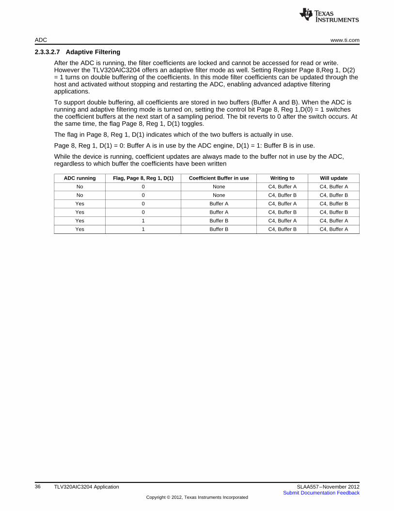
ADC www.ti.com
2.3.3.2.7 Adaptive Filtering
After the ADC is running, the filter coefficients are locked and cannot be accessed for read or write.However the TLV320AIC3204 offers an adaptive filter mode as well. Setting Register Page 8,Reg 1, D(2)= 1 turns on double buffering of the coefficients. In this mode filter coefficients can be updated through thehost and activated without stopping and restarting the ADC, enabling advanced adaptive filteringapplications.
To support double buffering, all coefficients are stored in two buffers (Buffer A and B). When the ADC isrunning and adaptive filtering mode is turned on, setting the control bit Page 8, Reg 1,D(0) = 1 switchesthe coefficient buffers at the next start of a sampling period. The bit reverts to 0 after the switch occurs. Atthe same time, the flag Page 8, Reg 1, D(1) toggles.
The flag in Page 8, Reg 1, D(1) indicates which of the two buffers is actually in use.
Page 8, Reg 1, D(1) = 0: Buffer A is in use by the ADC engine, D(1) = 1: Buffer B is in use.
While the device is running, coefficient updates are always made to the buffer not in use by the ADC,regardless to which buffer the coefficients have been written
ADC running Flag, Page 8, Reg 1, D(1) Coefficient Buffer in use Writing to Will update
No 0 None C4, Buffer A C4, Buffer A
No 0 None C4, Buffer B C4, Buffer B
Yes 0 Buffer A C4, Buffer A C4, Buffer B
Yes 0 Buffer A C4, Buffer B C4, Buffer B
Yes 1 Buffer B C4, Buffer A C4, Buffer A
Yes 1 Buffer B C4, Buffer B C4, Buffer A
36 TLV320AIC3204 Application SLAA557–November 2012Submit Documentation Feedback
Copyright © 2012, Texas Instruments Incorporated

www.ti.com ADC
2.3.3.3 ADC Setup
The following discussion is intended to guide a system designer through the steps necessary to configurethe TLV320AIC3204 ADC.
Step 1
The system clock source (master clock) and the targeted ADC sampling frequency must be identified.
Depending on the targeted performance, the decimation filter type (A, B or C) and OSR value can bedetermined.
• Filter A with AOSR of 128 should be used for 48kHz high performance operation.
• Filter B with AOSR of 64 should be used for 96kHz operations.
In conjunction with a common mode setting of 0.75V and PTM_R1 this can also be used for 48kHzPowerTune operation.
• Filter C with AOSR of 32 should be used for 192kHz operations
The oversampling ratio (OSR) of the TLV320AIC3204 must be configured to match the properties of thedigital microphone.
Based on the identified filter type and the required signal processing capabilities the appropriateprocessing block can be determined from the list of available processing blocks (PRB_R1 to PRB_R18)(See Table 2-7).
Based on the available master clock, the chosen OSR and the targeted sampling rate, the clock dividervalues NADC and MADC can be determined. If necessary the internal PLL will add a large degree offlexibility.
In summary, Codec_Clkin which is either derived directly from the system clock source or from the internalPLL, divided by MADC, NADC and AOSR, must be equal to the ADC sampling rate ADC_or fS. Thecodec_clkin clock signal is shared with the DAC clock generation block.
CODEC_CLKIN = NADC * MADC * AOSR * ADC_FS
To a large degree NADC and MADC can be chosen independently in the range of 1 to 128. In generalNADC should be as large as possible as long as the following condition can still be met:
MADC * AOSR / 32 ≥ RC
RC is a function of the chosen processing block, and is listed in Table 2-7.
The common mode setting of the device is determined by the available analog power supply and thedesired PowerTune mode; this common mode setting is shared across ADC, DAC (input common mode)and analog bypass path.
At this point the following device specific parameters are known:
PRB_Rx, AOSR, NADC, MADC, common mode setting
Additionally if the PLL is used the PLL parameters P, J, D and R are determined as well.
Step 2
Setting up the device via register programming:
The following list gives a sequence of items that must be executed between powering up the device andreading data from the device:
Define starting point: Set register page to 0Initiate SW Reset
Program Clock Settings Program PLL clock dividers P,J,D,R (if PLL is necessary)Power up PLL (if PLL is necessary)Program and power up NADCProgram and power up MADCProgram OSR valueProgram the processing block to be used
37SLAA557–November 2012 TLV320AIC3204 ApplicationSubmit Documentation Feedback
Copyright © 2012, Texas Instruments Incorporated

DAC www.ti.com
At this point, at the latest, the analog power supply must be applied to the device (via internal LDOor external).
Program Analog Blocks Set register Page to 1Disable coarse AVdd generationEnable Master Analog Power ControlProgram Common Mode voltageProgram PowerTune (PTM) modeProgram MicPGA startup delayProgram Reference fast chargingRouting of inputs and common mode to ADC inputUnmute analog PGAs and set analog gain
Power Up ADC Set register Page to 0Power up ADC ChannelsUnmute digital volume control
A detailed example can be found in Chapter 4.
2.4 DAC
The TLV320AIC3204 includes a stereo audio DAC supporting data rates from 8kHz to 192kHz. Eachchannel of the stereo audio DAC consists of a signal-processing engine with fixed processing blocks, adigital interpolation filter, multi-bit digital delta-sigma modulator, and an analog reconstruction filter. TheDAC is designed to provide enhanced performance at low sampling rates through increased oversamplingand image filtering, thereby keeping quantization noise generated within the delta-sigma modulator andsignal images strongly suppressed within the audio band to beyond 20kHz. To handle multiple input ratesand optimize power dissipation and performance, the TLV320AIC3204 allows the system designer toprogram the oversampling rates over a wide range from 1 to 1024. The system designer can choosehigher oversampling ratios for lower input data rates and lower oversampling ratios for higher input datarates.
The TLV320AIC3204 DAC channel includes a built-in digital interpolation filter to generate oversampleddata for the sigma-delta modulator. The interpolation filter can be chosen from three different typesdepending on required frequency response, group delay and sampling rate.
The DAC path of the TLV320AIC3204 features many options for signal conditioning and signal routing:
• 2 headphone amplifiers
– Usable in single-ended or differential mode
– Analog volume setting with a range of -6 to +29dB
– Class-D mode
• 2 line-out amplifiers
– Usable in single-ended or differential mode
– Analog volume setting with a range of -6 to +29dB
• Digital volume control with a range of -63.5 to +24dB
• Mute function
• Dynamic range compression (DRC)
In addition to the standard set of DAC features the TLV320AIC3204 also offers the following specialfeatures:
• Built in sine wave generation (beep generator)
• Digital auto mute
• Adaptive filter mode
The TLV320AIC3204 implements signal processing capabilities and interpolation filtering via processingblocks. These fixed processing blocks give users the choice of how much and what type of signalprocessing they may use and which interpolation filter is applied.
38 TLV320AIC3204 Application SLAA557–November 2012Submit Documentation Feedback
Copyright © 2012, Texas Instruments Incorporated
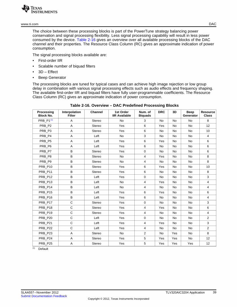
www.ti.com DAC
The choice between these processing blocks is part of the PowerTune strategy balancing powerconservation and signal processing flexibility. Less signal processing capability will result in less powerconsumed by the device. Table 2-16 gives an overview over all available processing blocks of the DACchannel and their properties. The Resource Class Column (RC) gives an approximate indication of powerconsumption.
The signal processing blocks available are:
• First-order IIR
• Scalable number of biquad filters
• 3D – Effect
• Beep Generator
The processing blocks are tuned for typical cases and can achieve high image rejection or low groupdelay in combination with various signal processing effects such as audio effects and frequency shaping.The available first-order IIR and biquad filters have fully user-programmable coefficients. The ResourceClass Column (RC) gives an approximate indication of power consumption.
Table 2-16. Overview – DAC Predefined Processing Blocks
Processing Interpolation Channel 1st Order Num. of DRC 3D Beep ResourceBlock No. Filter IIR Available Biquads Generator Class
PRB_P1 (1) A Stereo No 3 No No No 8
PRB_P2 A Stereo Yes 6 Yes No No 12
PRB_P3 A Stereo Yes 6 No No No 10
PRB_P4 A Left No 3 No No No 4
PRB_P5 A Left Yes 6 Yes No No 6
PRB_P6 A Left Yes 6 No No No 6
PRB_P7 B Stereo Yes 0 No No No 6
PRB_P8 B Stereo No 4 Yes No No 8
PRB_P9 B Stereo No 4 No No No 8
PRB_P10 B Stereo Yes 6 Yes No No 10
PRB_P11 B Stereo Yes 6 No No No 8
PRB_P12 B Left Yes 0 No No No 3
PRB_P13 B Left No 4 Yes No No 4
PRB_P14 B Left No 4 No No No 4
PRB_P15 B Left Yes 6 Yes No No 6
PRB_P16 B Left Yes 6 No No No 4
PRB_P17 C Stereo Yes 0 No No No 3
PRB_P18 C Stereo Yes 4 Yes No No 6
PRB_P19 C Stereo Yes 4 No No No 4
PRB_P20 C Left Yes 0 No No No 2
PRB_P21 C Left Yes 4 Yes No No 3
PRB_P22 C Left Yes 4 No No No 2
PRB_P23 A Stereo No 2 No Yes No 8
PRB_P24 A Stereo Yes 5 Yes Yes No 12
PRB_P25 A Stereo Yes 5 Yes Yes Yes 12(1) Default
39SLAA557–November 2012 TLV320AIC3204 ApplicationSubmit Documentation Feedback
Copyright © 2012, Texas Instruments Incorporated
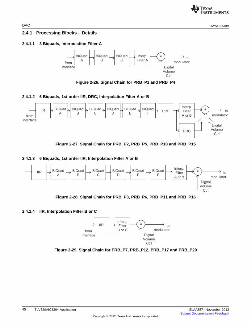
Interp.
Filter
B or C*IIR to
modulator
Digital
Volume
Ctrl
from
interface
Interp.
Filter
A or B*BiQuad
F
BiQuad
E
BiQuad
D
BiQuad
C
BiQuad
B
BiQuad
AIIR to
modulator
Digital
Volume
Ctrl
Interp.
Filter
A or B*
DRC
HPFBiQuad
F
BiQuad
E
BiQuad
D
BiQuad
C
BiQuad
B
BiQuad
AIIR to
modulator
Digital
Volume
Ctrl
from
interface
Interp.
Filter A *BiQuad
C
BiQuad
B
BiQuad
Ato
modulator
Digital
Volume
Ctrl
from
interface
DAC www.ti.com
2.4.1 Processing Blocks – Details
2.4.1.1 3 Biquads, Interpolation Filter A
Figure 2-26. Signal Chain for PRB_P1 and PRB_P4
2.4.1.2 6 Biquads, 1st order IIR, DRC, Interpolation Filter A or B
Figure 2-27. Signal Chain for PRB_P2, PRB_P5, PRB_P10 and PRB_P15
2.4.1.3 6 Biquads, 1st order IIR, Interpolation Filter A or B
Figure 2-28. Signal Chain for PRB_P3, PRB_P6, PRB_P11 and PRB_P16
2.4.1.4 IIR, Interpolation Filter B or C
Figure 2-29. Signal Chain for PRB_P7, PRB_P12, PRB_P17 and PRB_P20
40 TLV320AIC3204 Application SLAA557–November 2012Submit Documentation Feedback
Copyright © 2012, Texas Instruments Incorporated

Interp.
Filter C *BiQuad
D
BiQuad
C
BiQuad
B
BiQuad
AIIR to
modulator
Digital
Volume
Ctrl
from
interface
Interp.
Filter C *
DRC
HPFIIR to
modulator
Digital
Volume
Ctrl
BiQuad
D
BiQuad
C
BiQuad
B
BiQuad
Afrom
interface
Interp.
Filter B *BiQuad
D
BiQuad
C
BiQuad
B
BiQuad
Ato
modulator
Digital
Volume
Ctrl
from
interface
Interp.
Filter B *
DRC
HPF to
modulator
Digital
Volume
Ctrl
BiQuad
D
BiQuad
C
BiQuad
B
BiQuad
Afrom
interface
www.ti.com DAC
2.4.1.5 4 Biquads, DRC, Interpolation Filter B
Figure 2-30. Signal Chain for PRB_P8 and PRB_P13
2.4.1.6 4 Biquads, Interpolation Filter B
Figure 2-31. Signal Chain for PRB_P9 and PRB_P14
2.4.1.7 4 Biquads, 1st order IIR, DRC, Interpolation Filter C
Figure 2-32. Signal Chain for PRB_P18 and PRB_P21
2.4.1.8 4 Biquads, 1st order IIR, Interpolation Filter C
Figure 2-33. Signal Chain for PRB_P19 and PRB_P22
41SLAA557–November 2012 TLV320AIC3204 ApplicationSubmit Documentation Feedback
Copyright © 2012, Texas Instruments Incorporated

BiQuad
AL
Interp.
Filter A*
DRC
BiQuad
FL
BiQuad
EL
BiQuad
AR
IIR
left
3D
PGA
+
+
Interp.
Filter A*
DRC
BiQuad
FR
BiQuad
ER
BiQuad
DR
BiQuad
CR
BiQuad
BR
IIR
right+
+
-
+
-
+
+
from
left
channel
interface
to
modulator
to
modulator
Digital
Volume
Ctrl
Digital
Volume
Ctrl
from
right
channel
interface
BiQuad
BL
BiQuad
CL
BiQuad
DL
HPF
HPF
BiQuad
AL
Interp.
Filter A *
BiQuad
AR
IIR
left
3D
PGA
+
+
BiQuad
CR
BiQuad
BR
IIR
right +
+
-
+
-
+
+
from
left
channel
interface
to
modulator
Digital
Volume
Ctrl
from
right
channel
interface
BiQuad
BL
BiQuad
CL
Interp.
Filter A * to
modulator
Digital
Volume
Ctrl
DAC www.ti.com
2.4.1.9 2 Biquads, 3D, Interpolation Filter A
Figure 2-34. Signal Chain for PRB_P23
2.4.1.10 5 Biquads, DRC, 3D, Interpolation Filter A
Figure 2-35. Signal Chain for PRB_P24
42 TLV320AIC3204 Application SLAA557–November 2012Submit Documentation Feedback
Copyright © 2012, Texas Instruments Incorporated

11
23
110
zD2
zNN)z(H
-
-
-
+
=
BiQuad
AL
Interp.
Filter A* +
DRC
HPFBiQuad
FL
BiQuad
EL
BiQuad
AR
IIR
left
3D
PGA
+
+
Interp.
Filter A* +
DRC
*
Beep
Gen.
BiQuad
FR
BiQuad
ER
BiQuad
DR
BiQuad
CR
BiQuad
BR
IIR
right+
+
-
+
-
+
+
from
left
channel
interface
to
modulator
to
modulator
Digital
Volume
Ctrl
Digital
Volume
Ctrl
Beep
Volume
Ctrl
from
right
channel
interface
BiQuad
BL
BiQuad
CL
BiQuad
DL
*
HPF
www.ti.com DAC
2.4.1.11 5 Biquads, DRC, 3D, Beep Generator, Interpolation Filter A
Figure 2-36. Signal Chain for PRB_P25
2.4.2 User Programmable Filters
Depending on the selected processing block, different types and orders of digital filtering are available. Upto 6 biquad sections are available for specific processing blocks.
The coefficients of the available filters are arranged as sequentially-indexed coefficients in two banks. Ifadaptive filtering is chosen, the coefficient banks can be switched on-the-fly. For more details on adaptivefiltering please see Section 2.4.5.3.
The coefficients of these filters are each 24-bits wide, in two's-complement and occupy 3 consecutive 8-bitregisters in the register space. For default values please see the default values tables in the Register Mapsection.
2.4.2.1 First Order IIR Section
The IIR is of first-order and its transfer function is given by
(10)
The frequency response for the first order IIR Section with default coefficients is flat. Details on DACcoefficient default values are given in Section 5.13.
Table 2-17. DAC IIR Filter Coefficients
Filter Filter Coefficient ADC Coefficient Left Channel ADC Coefficient RightChannel
First order IIR N0 C65 (Page 46, Registers C68 (Page 46, Registers28,29,30) 40,41,42)
N1 C66 (Page 46, Registers C69 (Page 46, Registers32,33,34) 44,45,46)
D1 C67 (Page 46, Registers V70 (Page 46, Registers36,37,38) 48,49,50)
43SLAA557–November 2012 TLV320AIC3204 ApplicationSubmit Documentation Feedback
Copyright © 2012, Texas Instruments Incorporated

22
11
23
22
110
zDzD*22
zNzN*2N)z(H
--
--
--
++
=
DAC www.ti.com
2.4.2.2 Biquad Section
The transfer function of each of the Biquad Filters is given by
(11)
The frequency response for each biquad section with default coefficients is flat at a gain of 0dB. Details onDAC coefficient default values are given in Section 5.13.
Table 2-18. DAC Biquad Filter Coefficients
Filter Coefficient Left DAC Channel Right DAC Channel
BIQUAD A N0 C1 (Page 44, Registers 12,13,14) C33 (Page 45, Registers 20,21,22)
N1 C2 (Page 44, Registers 16,17,18) C34 (Page 45, Registers 24,25,26)
N2 C3 (Page 44, Registers 20,21,22) C35 (Page 45, Registers 28,29,30)
D1 C4 (Page 44, Registers 24,25,26) C36 (Page 45, Registers 32,33,34)
D2 C5 (Page 44, Registers 28,29,30) C37 (Page 45, Registers 36,37,38)
BIQUAD B N0 C6 (Page 44, Registers 32,33,34) C38 (Page 45, Registers 40,41,42)
N1 C7 (Page 44, Registers 36,37,38) C39 (Page 45, Registers 44,45,46)
N2 C8 (Page 44, Registers 40,41,42) C40 (Page 45, Registers 48,49,50)
D1 C9 (Page 44, Registers 44,45,46) C41 (Page 45, Registers 52,53,54)
D2 C10 (Page 44, Registers 48,49,50) C42 (Page 45, Registers 56,57,58)
BIQUAD C N0 C11 (Page 44, Registers 52,53,54) C43 (Page 45, Registers 60,61,62)
N1 C12 (Page 44, Registers 56,57,58) C44 (Page 45, Registers 64,65,66)
N2 C13 (Page 44, Registers 60,61,62) C45 (Page 45, Registers 68,69,70)
D1 C14 (Page 44, Registers 64,65,66) C46 (Page 45, Registers 72,73,74)
D2 C15 (Page 44, Registers 68,69,70) C47 (Page 45, Registers 76,77,78)
BIQUAD D N0 C16 (Page 44, Registers 72,73,74) C48 (Page 45, Registers 80,81,82)
N1 C17 (Page 44, Registers 76,77,78) C49 (Page 45, Registers 84,85,86)
N2 C18 (Page 44, Registers 80,81,82) C50 (Page 45, Registers 88,89,90)
D1 C19 (Page 44, Registers 84,85,86) C51 (Page 45, Registers 92,93,94)
D2 C20 (Page 44, Registers 88,89,90) C52 (Page 45, Registers 96,97,98)
BIQUAD E N0 C21 (Page 44, Registers 92,93,94) C53 (Page 45, Registers 100,101,102)
N1 C22 (Page 44, Registers 96,97,98) C54 (Page 45, Registers 104,105,106)
N2 C23 (Page 44, Registers 100,101,102) C55 (Page 45, Registers 108,109,110)
D1 C24 (Page 44, Registers 104,105,106) C56 (Page 45, Registers 112,113,114)
D2 C25 (Page 44, Registers 108,109,110) C57 (Page 45, Registers 116,117,118)
BIQUAD F N0 C26 (Page 44, Registers 112,113,114) C58 (Page 45, Registers 120,121,122)
N1 C27 (Page 44, Registers 116,117,118) C59 (Page 45, Registers 124,125,126)
N2 C28 (Page 44, Registers 120,121,122) C60 (Page 46, Registers 8,9,10)
D1 C29 (Page 44, Registers 124,125,126) C61 (Page 46, Registers 12,13,14)
D2 C30 (Page 45, Registers 8,9,10) C62 (Page 46, Registers 16,17,18)
2.4.2.2.1 3D-PGA
The 3D-PGA attenuation block as used in the processing blocks PRB_P23, PRB_P24 and PRB_P25 canbe programmed in the range of -1.0 to +1.0. A value of -1.0 corresponds to 0x7FFFFF in DAC coefficientC32 (Page 45, Register 16,17 and 18). A value of 1.0 corresponds to 0x800000 in coefficient C32.
44 TLV320AIC3204 Application SLAA557–November 2012Submit Documentation Feedback
Copyright © 2012, Texas Instruments Incorporated

0
–10
–20
–30
–40
–50
–60
–70
–80
–90
1 2 3 4 5 6 7
Frequency Normalized to fS
Magnitude
–dB
DAC Channel Response for Interpolation Filter A(Red line corresponds to –65 dB)
G016
www.ti.com DAC
2.4.3 Interpolation Filters
2.4.3.1 Interpolation Filter A
Filter A is designed for an fS up to 48ksps with a flat passband of 0kHz–20kHz.
Table 2-19. DAC Interpolation Filter A, Specification
Parameter Condition Value (Typical) Units
Filter Gain Pass Band 0 … 0.45fS ±0.015 dB
Filter Gain Stop Band 0.55… 7.455fS –65 dB
Filter Group Delay 21 / fS s
Figure 2-37. DAC Interpolation Filter A, Frequency Response
2.4.3.2 Interpolation Filter B
Filter B is specifically designed for an fS of above 96ksps. Thus, the flat pass-band region easily coversthe required audio band of 0-20kHz.
Table 2-20. DAC Interpolation Filter B, Specification
Parameter Condition Value (Typical) Units
Filter Gain Pass Band 0 … 0.45fS ±0.015 dB
Filter Gain Stop Band 0.55… 3.45fS –58 dB
Filter Group Delay 18 / fS s
45SLAA557–November 2012 TLV320AIC3204 ApplicationSubmit Documentation Feedback
Copyright © 2012, Texas Instruments Incorporated

DAC Channel Response for Interpolation Filter C(Red line corresponds to –43 dB)
0
–10
–20
–30
–40
–50
–60
–70
0.0 0.2 0.4 0.6 0.8 1.0 1.4
Frequency Normalized to fS
Magnitude
–dB
G018
1.2
0
–10
–20
–30
–40
–50
–60
–70
–80
0.5 1.0 1.5 2.0 2.5 3.0 3.5
Frequency Normalized to fS
Magnitude
–dB
G017
DAC Channel Response for Interpolation Filter B(Red line corresponds to –58 dB)
DAC www.ti.com
Figure 2-38. Channel Interpolation Filter B, Frequency Response
2.4.3.3 Interpolation Filter C
Filter C is specifically designed for the 192ksps mode. The pass band extends up to 0.40 * fS (correspondsto 80kHz), more than sufficient for audio applications.
Figure 2-39. DAC Interpolation Filter C, Frequency Response
Table 2-21. DAC Interpolation Filter C, Specification
Parameter Condition Value (Typical) Units
Filter Gain Pass Band 0 … 0.35fS ±0.03 dB
Filter Gain Stop Band 0.60… 1.4fS –43 dB
Filter Group Delay 13 / fS s
46 TLV320AIC3204 Application SLAA557–November 2012Submit Documentation Feedback
Copyright © 2012, Texas Instruments Incorporated

www.ti.com DAC
2.4.4 DAC Gain Setting
2.4.4.1 PowerTune Modes
As part of the PowerTune strategy, the analog properties of the DAC are adjusted. As a consequence, thefull-scale signal swing achieved at the headphone and line outputs must be adjusted.
Please see Table 2-22 for the proper gain compensation values across the different combinations.
Table 2-22. DAC Gain versus. PowerTune Modes
DAC PowerTune PowerTune Mode Headphone or Line-out GainMode Control
Page 1,Register 3 or CM = 0.75V, Gain for 375mVRMS output CM = 0.9V, Gain for 500mVRMS output4, D(4:2) swing at 0dB full scale input swing at 0dB full scale input
000 PTM_P3, PTM_P4 –2 0
001 PTM_P2 2 4
010 PTM_P1 12 14
2.4.4.2 Digital Volume Control
The TLV320AIC3204 signal processing blocks incorporate a digital volume control block that can controlthe volume of the playback signal from +24dB to –63.5dB in steps of 0.5dB. These can be controlled bywriting to Page 0, Register 65 and 66. The volume control of left and right channels by default can becontrolled independently, however by programming Page 0, Reg 64, D(1:0), they can be madeinterdependent. The volume changes are soft-stepped in steps of 0.5dB to avoid audible artifacts duringgain change. The rate of soft-stepping can be controlled by programming Page 0, Reg 63, D(1:0) to eitherone step per frame (DAC_FS) or one step per 2 frames. The soft-stepping feature can also be entirelydisabled. During soft-stepping the value of the actual applied gain would differ from the programmed gainin register. The TLV320AIC3204 gives a feedback to the user in form of register readable flag to indicatethat soft-stepping is currently in progress. The flags for left and right channels can be read back byreading Page 0, Reg 38, Bits D4 and D0 respectively. A value of 0 in these flags indicates a soft-steppingoperation in progress, and a value of 1 indicates that soft-stepping has completed. A soft-steppingoperation comes into effect during
(a) power-up, when the volume control soft-steps from –63.5dB to programmed gain value,
(b) volume change by user when DAC is powered up, and
(c) power-down, when the volume control block soft-steps to –63.5dB before powering down the channel.
2.4.4.3 Dynamic Range Compression
Typical music signals are characterized by crest factors, the ratio of peak signal power to average signalpower, of 12dB or more. To avoid audible distortion due to clipping of peak signals, the gain of the DACchannel must be adjusted to prevent hard clipping of peak signals. As a result, during nominal periods, theapplied gain is low, causing the perception that the signal is not loud enough. To overcome this problem,the DRC in the TLV320AIC3204 continuously monitors the output of the DAC Digital Volume control todetect its power level w.r.t. 0dBFS. When the power level is low, it increases the input signal gain to makeit sound louder. At the same time, if a peaking signal is detected, it autonomously reduces the appliedgain to avoid hard clipping. The resulting sound can be more pleasing to the ear as well as soundinglouder during nominal periods.
The DRC functionality in the TLV320AIC3204 is implemented by a combination of Processing Blocks inthe DAC channel as described in Section 2.4.1.
The DRC can be disabled by writing into Page 0, Reg 68, D(6:5).
The DRC typically works on the filtered version of the input signal. The input signals have no audioinformation at DC and extremely low frequencies; however they can significantly influence the energyestimation function in DRC. Also most of the information about signal energy is concentrated in the lowfrequency region of the input signal.
47SLAA557–November 2012 TLV320AIC3204 ApplicationSubmit Documentation Feedback
Copyright © 2012, Texas Instruments Incorporated

11
23
110
LPFzD2
zNN)z(H
-
-
-
+
=
11
23
110
HPFzD2
zNN)z(H
-
-
-
+
=
DAC www.ti.com
In order to estimate the energy of the input signal, the signal is first fed to the DRC high-pass filter andthen to the DRC low-pass filter. These filters are implemented as first-order IIR filters given by
(12)
(13)
The coefficients for these filters are 24-bits wide in two’s-complement and are user programmable throughregister write as given in Table 2-23, and coefficient default values are summarized in Section 5.13.
Table 2-23. DRC HPF and LPF Coefficients
Coefficient Location
HPF N0 C71 Page 46, Register 52 to 55
HPF N1 C72 Page 46, Register 56 to 59
HPF D1 C73 Page 46, Register 60 to 63
LPF N0 C74 Page 46, Register 64 to 67
LPF N1 C75 Page 46, Register 68 to 71
LPF D1 C76 Page 46, Register 72 to 75
The default values of these coefficients implement a high-pass filter with a cut-off at 0.00166 * DAC_FS,and a low-pass filter with a cutoff at 0.00033 * DAC_FS.
The output of the DRC high-pass filter is fed to the Processing Block selected for the DAC Channel. Theabsolute value of the DRC-LPF filter is used for energy estimation within the DRC.
The gain in the DAC Digital Volume Control is controlled by Page 0, Register 65 and 66. When the DRC isenabled, the applied gain is a function of the Digital Volume Control register setting and the output of theDRC.
The DRC parameters are described in sections that follow.
2.4.4.3.1 DRC Threshold
The DRC Threshold represents the level of the DAC playback signal at which the gain compressionbecomes active. The output of the digital volume control in the DAC is compared with the set threshold.The threshold value is programmable by writing to register Page 0, Register 68, D(4:2). The Thresholdvalue can be adjusted between –3dBFS to –24dBFS in steps of 3dB. Keeping the DRC Threshold valuetoo high may not leave enough time for the DRC block to detect peaking signals, and can causeexcessive distortion at the outputs. Keeping the DRC Threshold value too low can limit the perceivedloudness of the output signal.
The recommended DRC-Threshold value is –24dB.
When the output signal exceeds the set DRC Threshold, the interrupt flag bits at Page 0, Register 44,D(3:2) are updated. These flag bits are 'sticky' in nature, and are reset only after they are read back by theuser. The non-sticky versions of the interrupt flags are also available at Page 0, Register 46, D(3:2).
2.4.4.3.2 DRC Hysteresis
DRC Hysteresis is programmable by writing to Page 0, Register 68, D(1:0) with values between 0dB and3dB in steps of 1dB. DRC Hysteresis is a programmable window around the programmed DRC Thresholdthat must be exceeded for a disabled DRC to become enabled, or an enabled DRC to become disabled.For example, if the DRC Threshold is set to –12dBFS and DRC Hysteresis is set to 3dB, then if the gaincompressions in the DRC is inactive, the output of the DAC Digital Volume Control must exceed –9dBFSbefore gain compression due to the DRC is activated. Similarly, when the gain compression in the DRC is
48 TLV320AIC3204 Application SLAA557–November 2012Submit Documentation Feedback
Copyright © 2012, Texas Instruments Incorporated
www.ti.com DAC
active, the output of the DAC Digital Volume Control must fall below –15dBFS for gain compression in theDRC to be deactivated. The DRC Hysteresis feature prevents the rapid activation and de-activation ofgain compression in the DRC in cases when the output of DAC Digital Volume Control rapidly fluctuates ina narrow region around the programmed DRC Threshold. Programming the DRC Hysteresis as 0dBdisables the hysteresis action.
Recommended Value of DRC Hysteresis is 3dB.
2.4.4.3.3 DRC Hold
The DRC Hold function slows the start of decay for a specified period of time in response to a decrease inenergy level. To minimize audible artifacts, it is recommended to set the DRC Hold time to 0 throughprogramming Page 0, Register 69, D(6:3) = 0000.
2.4.4.3.4 DRC Attack Rate
When the output of the DAC Digital Volume Control exceeds the programmed DRC Threshold, the gainapplied in the DAC Digital Volume Control is progressively reduced to avoid the signal from saturating thechannel. This process of reducing the applied gain is called Attack. To avoid audible artifacts, the gain isreduced slowly with a rate equaling the Attack Rate programmable via Page 0, Register 70, D(7:4). AttackRates can be programmed from 4dB gain change per sample period (1 / DAC_FS) to 1.2207e-5dB gainchange per sample period.
Attack Rates should be programmed such that before the output of the DAC Digital Volume control canclip, the input signal should be sufficiently attenuated. High Attack Rates can cause audible artifacts, andtoo-slow Attack Rates may not prevent the input signal from clipping.
The recommended DRC Attack Rate value is 1.9531e-4 dB per sample period.
2.4.4.3.5 DRC Decay Rate
When the DRC detects a reduction in output signal swing beyond the programmed DRC Threshold, theDRC enters a Decay state, where the applied gain in Digital Volume Control is gradually increased toprogrammed values. To avoid audible artifacts, the gain is slowly increased with a rate equal to the DecayRate programmed through Page 0, Register 70, D(3:0). The Decay Rates can be programmed from1.5625e-3dB per sample period to 4.7683e-7dB per sample period. If the Decay Rates are programmedtoo high, then sudden gain changes can cause audible artifacts. However, if it is programmed too slow,then the output may be perceived as too low for a long time after the peak signal has passed.
The recommended Value of DRC Decay Rate is 2.4414e-5 dB per sample period.
2.4.4.3.6 Example Setup for DRC• PGA Gain = 12dB
• Threshold = -24dB
• Hysteresis = 3dB
• Hold time = 0ms
• Attack Rate = 1.9531e-4 dB per sample period
• Decay Rate = 2.4414e-5 dB per sample period
Script
w 30 00 00 #Go to Page 0w 30 41 18 #DAC => 12 db gain leftw 30 42 18 #DAC => 12 db gain rightw 30 44 7F #DAC => DRC Enabled for both channels, Threshold = -24 db, Hysteresis = 3 dBw 30 45 00 #DRC Hold = 0 ms, Rate of Changes of Gain = 0.5 dB/Fs'w 30 46 B6 #Attack Rate = 1.9531e-4 dB/Frame , DRC Decay Rate =2.4414e-5 dB/Framew 30 00 2E #Go to Page 46w 30 34 7F AB 00 00 80 55 00 00 7F 56 00 00 #DRC HPFw 30 40 00 11 00 00 00 11 00 00 7F DE 00 00 #DRC LPF
49SLAA557–November 2012 TLV320AIC3204 ApplicationSubmit Documentation Feedback
Copyright © 2012, Texas Instruments Incorporated
DAC www.ti.com
2.4.5 DAC Special Functions
2.4.5.1 Beep Generation
A special function has also been included in the processing block PRB_P25 for generating a digital sine-wave signal that is sent to the DAC. This signal is intended for generating key-click sounds for userfeedback. A default value for the sine-wave frequency, sine burst length, and signal magnitude is kept inthe Tone Generator Registers Page 0, Registers 71 through 79. The sine wave generator is very flexible,and is completely register programmable via 9 registers of 8 bits each to provide many different sounds.
Two registers are used for programming the 16-bit, two's-complement, sine-wave coefficient (Page 0,Registers 76 and 77). Two other registers program the 16-bit, two's-complement, cosine-wave coefficient(Page 0, Registers 78 and 79). This coefficient resolution allows virtually any frequency of sine wave in theaudio band to be generated up to DAC_FS / 2.
Three registers are used to control the length of the sine burst waveform which are located on Page 0,Registers 73, 74, and 75. The resolution (bit) in the registers of the sine burst length is one sample time,so this allows great control on the overall time of the sine burst waveform. This 24-bit length timersupports 16,777,215 sample times. (For example if DAC_FS is set at 48kHz, and the registers combinedvalue equals 96000d (01770h), then the sine burst would last exactly two seconds.)
Separate registers independently control the Left sine-wave volume and the Right sine-wave volume. The6-bit digital volume control allows level control of 0dB to –63dB in one-dB steps. The left-channel volumeis controlled by writing to Page 0, Register 71, D(5:0). The right-channel volume is controlled by Page 0,Register 72, D(5:0). A master volume control for the left and right channel of the beep generator can beset up using Page 0, Register 72, D(7:6). The default volume control setting is 0dB, the tone generatormaximum-output level.
To play back the sine wave, the DAC must be configured with regards to clock setup and routing. The sinewave starts by setting the Beep Generator Enable Bit (Page 1, Register 71, D(7) = 1). After the sine wavehas played for its predefined time period this bit automatically resets back to 0. While the sine wave isplaying, the parameters of the beep generator cannot be changed. To stop the sine wave before thepredefined time period expires, set the Beep Generator Enable Bit to 0.
2.4.5.2 Digital Auto Mute
The TLV320AIC3204 also incorporates a special feature where the DAC channel is auto-muted when acontinuous stream of DC-input is detected. By default, this feature is disabled, and is enabled by writing anon-zero value into Page 0, Register 64, D(6:4). This non-zero value controls the duration of thecontinuous stream of DC-input before the auto-mute feature takes effect. This feature is especially helpfulfor eliminating high-frequency noise power from being delivered into the load during silent periods ofspeech or music.
2.4.5.3 Adaptive Filtering
When the DAC is running, the user-programmable filter coefficients are locked and cannot be accessedfor either read or write.
However the TLV320AIC3204 offers an adaptive filter mode as well. Setting Register Page 44, Reg 1, BitD(2) = 1 turns on double buffering of the coefficients. In this mode, filter coefficients can be updatedthrough the host, and activated without stopping and restarting the DAC. This enables advanced adaptivefiltering applications.
In the double-buffering scheme, all coefficients are stored in two buffers (Buffers A and B). When the DACis running and adaptive filtering mode is turned on, setting the control bit Page 44, Register 1, D(0) = 1switches the coefficient buffers at the next start of a sampling period. This bit resets back to 0 after theswitch occurs. At the same time, the flag (Page 44, Reg 1, D(1)) toggles.
The flag in Page 44, Register 1, D(1) indicates which of the two buffers is actually in use.
Page 44, Register 1, D(1) = 0: Buffer A is in use by the DAC engine, Bit D(1) = 1: Buffer B is in use.
While the device is running, coefficient updates are always made to the buffer not in use by the DAC,regardless to which buffer the coefficients have been written.
50 TLV320AIC3204 Application SLAA557–November 2012Submit Documentation Feedback
Copyright © 2012, Texas Instruments Incorporated
www.ti.com DAC
DAC running Page 44, Reg 1, Bit D1 Coefficient Buffer in use Writing to Will update
No 0 None C1, Buffer A C1, Buffer A
No 0 None C1, Buffer B C1, Buffer B
Yes 0 Buffer A C1, Buffer A C1, Buffer B
Yes 0 Buffer A C1, Buffer B C1, Buffer B
Yes 1 Buffer B C1, Buffer A C1, Buffer A
Yes 1 Buffer B C1, Buffer B C1, Buffer A
The user programmable coefficients C1 to C70 are defined on Pages 44, 45 and 46 for Buffer A andPages 62, 63 and 64 for Buffer B.
2.4.6 DAC Setup
This section lists the steps necessary to configure the TLV320AIC3204 DAC.
Step 1
Determine the system clock source (master clock) and the targeted DAC sampling frequency.
Choose the targeted performance. This drives the choice of the decimation filter type (A, B or C) andDOSR value.
Use Filter A for 48kHz high-performance operation; DOSR must be a multiple of 8.Use Filter B for up to 96kHz operations; DOSR must be a multiple of 4.Use Filter C for up to 192kHz operations; DOSR must be a multiple of 2.
In all cases the DOSR range is limited by the following condition:
2.8MHz < DOSR * DAC_FS < 6.2MHz
Based on the identified filter type and the required signal processing capabilities, the appropriateprocessing block is determined from the list of available processing blocks (PRB_P1 to PRB_P25).
Based on the available master clock, the chosen DOSR and the targeted sampling rate, the clock dividervalues NDAC and MDAC are calculated. If necessary, the internal PLL can add a large degree offlexibility.
In summary, codec_clkin (derived directly from the system clock source or from the internal PLL) dividedby MDAC, NDAC and DOSR must be equal to the DAC sampling rate DAC_FS. The codec_clkin clocksignal is shared with the ADC clock generation block.
CODEC_CLKIN = NDAC * MDAC * DOSR * DAC_FS
To a large degree, NDAC and MDAC can be chosen independently in the range of 1 to 128. In general,NDAC should be as large as possible as long as the following condition can still be met:
MDAC * DOSR / 32 ≥ RC
RC is a function of the chosen processing block and is listed in Table 2-16.
The common-mode voltage setting of the device is determined by the available analog power supply andthe desired PowerTune mode. This common-mode (input common-mode) value is common across theADC, DAC and analog bypass path. The output common-mode setting is determined by the availableanalog power supplies (AVDD and LDOIN) and the desired output-signal swing.
At this point the following device specific parameters are known:
PRB_Px, DOSR, NDAC, MDAC, input and output common-mode values
If the PLL is used, the PLL parameters P, J, D and R are determined as well.
51SLAA557–November 2012 TLV320AIC3204 ApplicationSubmit Documentation Feedback
Copyright © 2012, Texas Instruments Incorporated

PowerTune www.ti.com
Step 2
Setting up the device via register programming:
The following list gives a sequence of items that must be executed in the time between powering thedevice up and reading data from the device:
Define starting point: Set register page to 0Initiate SW Reset
Program Clock Settings Program PLL clock dividers P,J,D,R (if PLL is necessary)Power up PLL (if PLL is necessary)Program and power up NDACProgram and power up MDACProgram OSR valueProgram I2S word length if required (for example, 20bit)Program the processing block to be used
At this point, at the latest, the analog power supply must be applied to the device (via internal LDOor external)
Program Analog Blocks Set register Page to 1Disable coarse AVDD generationEnable Master Analog Power ControlProgram Common Mode voltageProgram PowerTune (PTM) modeProgram Reference fast chargingProgram Headphone specific depop settings (in case of headphone driverused)Program routing of DAC output to the output amplifier (headphone or lineout)Unmute and set gain of output driverPower up output driver
Apply waiting time determined by the de-pop settings and the soft-stepping settings of the drivergain or poll Page 1 , Register 63
Power Up DAC Set register Page to 0Power up DAC ChannelsUnmute digital volume control
A detailed example can be found in the Example Setups section.
2.5 PowerTune
The TLV320AIC3204 features PowerTune, a mechanism to balance power-versus-performance trade-offsat the time of device configuration. The device can be tuned to minimize power dissipation, to maximizeperformance, or to an operating point between the two extremes to best fit the application.
2.5.1 PowerTune Modes
2.5.1.1 ADC – Programming PTM_R1 to PTM_R4
The device powers up with PTM_R4 (highest performance) set as default. This mode always works acrossall combinations of common-mode voltage, chosen processing block, or chosen oversampling ratio. If theapplication can make use of a lower-power configuration please see the ADC and DAC powerconsumption chapters below for valid combination of PowerTune modes and other device parameters.
The ADC configuration of the PowerTune mode affects right and left channels simultaneously.
52 TLV320AIC3204 Application SLAA557–November 2012Submit Documentation Feedback
Copyright © 2012, Texas Instruments Incorporated
www.ti.com PowerTune
PTM_R1 PTM_R2 PTM_R3 PTM_R4
Pg 1, Reg 61, D(7:0) 0xFF 0xB6 0x64 0x00
2.5.1.2 DAC - Programming PTM_P1 to PTM_P4
On the playback side, the performance is determined by a combination of register settings and the audiodata word length applied. For the highest performance setting (PTM_P4), an audio-data word length of 20bits is required, while for the modes PTM_P1 to PTM_P3 a word length of 16 bits is sufficient.
PTM_P1 PTM_P2 PTM_P3 PTM_P4
Pg 1, Reg 3, D(4:2) 0x2 0x1 0x0 0x0
Pg 1, Reg 4, D(4:2) 0x2 0x1 0x0 0x0
Audio Data word length 16 bits 16 bits 16 bits 20 or more bits
Pg 0, Reg 27, D(5:4) 0x0 0x0 0x0 0x1, 0x2, 0x3
2.5.1.3 Processing Blocks
The choice of processing blocks, PRB_P1 to PRB_P25 for playback and PRB_R1 to PRB_R18 forrecording, also influences the power consumption. In fact, the numerous processing blocks have beenimplemented to offer a choice between power-optimization and configurations with more signal-processingresources.
2.5.2 ADC Power Consumption
The tables in this section give recommendations for various PowerTune modes. Typical performance andpower-consumption values are listed. PowerTune modes that are not supported are marked with an ‘X’.
All measurements were taken with the PLL turned off and the ADC configured for single-ended input. Thevalues given in the tables are intended as target-performance levels, not device specifications. For devicespecifications, see the TLV320AIC3204 data sheet, .
53SLAA557–November 2012 TLV320AIC3204 ApplicationSubmit Documentation Feedback
Copyright © 2012, Texas Instruments Incorporated

PowerTune www.ti.com
2.5.2.1 ADC, Stereo, 48kHz, Highest Performance, DVDD = 1.8V, AVDD = 1.8V
AOSR = 128, Processing Block = PRB_R1 (Decimation Filter A)
Device Common Mode Setting = 0.75V Device Common Mode Setting = 0.9V
PTM_R1 PTM_R2 PTM_R3 PTM_R4 PTM_R1 PTM_R2 PTM_R3 PTM_R4 UNIT
0dB full scale X 375 375 375 X 500 500 500 mVRMS
Max. allowed input level w.r.t. X –12 0 0 X –12 0 0 dB full0dB full scale scale
Effective SNR w.r.t. X 78.5 90.7 90.2 X 80.4 92.9 92.7 dBmax. allowed input level
Power consumption X 11.9 14.2 18.2 X 11.9 14.2 18.2 mW
Alternative processing blocks:
Processing Block Filter Est. Power Change (mW)
PRB_R2 A +1.4
PRB_R3 A +1.4
2.5.2.2 ADC, Stereo, 48kHz, DVDD = 1.8V, AVDD = 1.8V
AOSR = 64, Processing Block = PRB_R7 (Decimation Filter B)
Device Common Mode Setting = 0.75V Device Common Mode Setting = 0.9V
PTM_R1 PTM_R2 PTM_R3 PTM_R4 PTM_R1 PTM_R2 PTM_R3 PTM_R4 UNIT
0dB full scale 375 X 375 X X X 500 X mVRMS
Max. allowed input level w.r.t. –2 X 0 X X X 0 X dB full0dB full scale scale
Effective SNR w.r.t. 86.0 X 88.1 X X X 90.4 X dBmax. allowed input level
Power consumption 8.4 X 11.4 X X X 11.5 X mW
Alternative processing blocks:
Processing Block Filter Est. Power Change (mW)
PRB_R8 B +0.7
PRB_R9 B +0.7
PRB_R1 A +2.0
PRB_R2 A +3.4
PRB_R3 A +3.4
54 TLV320AIC3204 Application SLAA557–November 2012Submit Documentation Feedback
Copyright © 2012, Texas Instruments Incorporated

www.ti.com PowerTune
2.5.2.3 ADC, Stereo, 48kHz, Lowest Power Consumption
AOSR = 64, Processing Block = PRB_R7 (Decimation Filter B), DVDD = 1.26V
PTM_R1 PTM_R3 UNITCM = 0.75V CM = 0.9VAVDD=1.5V AVDD=1.8V
0dB full scale 375 500 mVRMS
Max. allowed input level w.r.t. 0dB –2 0 dB full scalefull scale
Effective SNR w.r.t. max. allowed 88.0 92.2 dBinput level
Power consumption 6.0 11.4 mW
Alternative processing blocks:
Processing Block Filter Est. Power Change (mW)
PRB_R8 B + 0.3
PRB_R9 B + 0.3
PRB_R1 A + 1.0
PRB_R2 A + 1.6
PRB_R3 A + 1.6
2.5.2.4 ADC, Mono, 48kHz, Highest Performance, DVDD = 1.8V, AVDD = 1.8V
AOSR = 128, Processing Block = PRB_R4 (Decimation Filter A)
Device Common Mode Setting = 0.75V Device Common Mode Setting = 0.9V
PTM_R1 PTM_R2 PTM_R3 PTM_R4 PTM_R1 PTM_R2 PTM_R3 PTM_R4 UNIT
0dB full scale X 375 375 375 X 500 500 500 mVRMS
Max. allowed input level w.r.t. X –12 0 0 X –12 0 0 dB full0dB full scale scale
Effective SNR w.r.t. X 78.3 90.8 90.6 X 80.3 92.8 92.7 dBmax. allowed input level
Power consumption X 9.1 11.4 15.4 X 9.1 11.4 15.4 mW
Alternative processing blocks:
Processing Block Filter Est. Power Change (mW)
PRB_R5 A +0.7
PRB_R6 A +0.7
55SLAA557–November 2012 TLV320AIC3204 ApplicationSubmit Documentation Feedback
Copyright © 2012, Texas Instruments Incorporated

PowerTune www.ti.com
2.5.2.5 ADC, Mono, 48kHz, DVDD = 1.8V, AVDD = 1.8V
AOSR = 64, Processing Block = PRB_R11 (Decimation Filter B)
Device Common Mode Setting = 0.75V Device Common Mode Setting = 0.9V
PTM_R1 PTM_R2 PTM_R3 PTM_R4 PTM_R1 PTM_R2 PTM_R3 PTM_R4 UNIT
0dB full scale 375 X 375 X X X 500 X mVRMS
Max. allowed input level w.r.t. –2 X 0 X X X 0 X dB full0dB full scale scale
Effective SNR w.r.t. 86.0 X 88.1 X X X 90.3 X dBmax. allowed input level
Power consumption 7.0 X 10.1 X X X 10.1 X mW
Alternative processing blocks:
Processing Block Filter Est. Power Change (mW)
PRB_R10 B 0
PRB_R12 B 0
PRB_R4 A +0.7
PRB_R5 A +1.4
PRB_R6 A +1.4
2.5.2.6 ADC, Mono, 48 kHz, Lowest Power Consumption,
AOSR = 64, Processing Block = PRB_R11 (Decimation Filter B), DVDD = 1.26V
PTM_R1 PTM_R3 UNITCM = 0.75V CM = 0.9VAVDD=1.5V AVDD=1.8V
0dB full scale 375 500 mVRMS
Max. allowed input level w.r.t. –2 0 dB full scale0dB full scale
Effective SNR w.r.t. 86.0 90.5 dBmax. allowed input level
Power consumption 5.1 9.2 mW
Alternative processing blocks:
Processing Block Filter Est. Power Change (mW)
PRB_R10 B 0
PRB_R12 B 0
PRB_R4 A +0.3
PRB_R5 A +0.7
PRB_R6 A +0.7
56 TLV320AIC3204 Application SLAA557–November 2012Submit Documentation Feedback
Copyright © 2012, Texas Instruments Incorporated

www.ti.com PowerTune
2.5.2.7 ADC, Stereo, 8kHz, Highest Performance, DVDD = 1.8V, AVDD = 1.8V
AOSR = 128, Processing Block = PRB_R1 (Decimation Filter A)
Device Common Mode Setting = 0.75V Device Common Mode Setting = 0.9V
PTM_R1 PTM_R2 PTM_R3 PTM_R4 PTM_R1 PTM_R2 PTM_R3 PTM_R4 UNIT
0dB full scale 375 X X X 500 X X X mVRMS
Max. allowed input level w.r.t. 0 X X X 0 X X X dB full0dB full scale scale
Effective SNR w.r.t. 91.1 X X X 93.2 X X X dBmax. allowed input level
Power consumption 6.5 X X X 6.5 X X X mW
Alternative processing blocks:
Processing Block Filter Est. Power Change (mW)
PRB_R2 A +0.2
PRB_R3 A +0.2
2.5.2.8 ADC, Stereo, 8kHz, DVDD = 1.8V, AVDD = 1.8V
AOSR = 64, Processing Block = PRB_R7 (Decimation Filter B)
Device Common Mode Setting = 0.75V Device Common Mode Setting = 0.9V
PTM_R1 PTM_R2 PTM_R3 PTM_R4 PTM_R1 PTM_R2 PTM_R3 PTM_R4 UNIT
0dB full scale 375 X X X 500 X X X mVRMS
Max. allowed input level w.r.t. 0 X X X 0 X X X dB full0dB full scale scale
Effective SNR w.r.t. 88.2 X X X 90.6 X X X dBmax. allowed input level
Power consumption 6.0 X X X 6.1 X X X mW
Alternative processing blocks:
Processing Block Filter Est. Power Change (mW)
PRB_R8 B + 0.1
PRB_R9 B + 0.1
PRB_R1 A + 0.3
PRB_R2 A +0.6
PRB_R3 A + 0.6
57SLAA557–November 2012 TLV320AIC3204 ApplicationSubmit Documentation Feedback
Copyright © 2012, Texas Instruments Incorporated

PowerTune www.ti.com
2.5.2.9 ADC, Stereo, 8kHz, Lowest Power Consumption,
AOSR = 64, Processing Block = PRB_R7 (Decimation Filter B), PowerTune Mode = PTM_R1, DVDD =1.26
CM = 0.75V CM = 0.9V UNITAVDD=1.5V AVDD=1.8V
0dB full scale 375 500 mVRMS
Max. allowed input level w.r.t. 0 0 dB full scale0dB full scale
Effective SNR w.r.t. 88.3 92.4 dBmax. allowed input level
Power consumption 4.7 5.8 mW
Alternative processing blocks:
Processing Block Filter Est. Power Change (mW)
PRB_R8 B + 0.1
PRB_R9 B + 0.1
PRB_R1 A + 0.2
PRB_R2 A + 0.3
PRB_R3 A + 0.3
2.5.2.10 ADC, Mono, 8kHz, Highest Performance, DVDD = 1.8V, AVDD = 1.8V
AOSR = 128, Processing Block = PRB_R4 (Decimation Filter A)
Device Common Mode Setting = 0.75V Device Common Mode Setting = 0.9V
PTM_R1 PTM_R2 PTM_R3 PTM_R4 PTM_R1 PTM_R2 PTM_R3 PTM_R4 UNIT
0dB full scale 375 X X X 500 X X X mVRMS
Max. allowed input level w.r.t. 0 X X X 0 X X X dB full0dB full scale scale
Effective SNR w.r.t. max. 88.5 X X X 93.3 X X X dBallowed input level
Power consumption 5.5 X X X 5.6 X X X mW
Alternative processing blocks:
Processing Block Filter Est. Power Change (mW)
PRB_R5 A +0.1
PRB_R6 A +0.1
58 TLV320AIC3204 Application SLAA557–November 2012Submit Documentation Feedback
Copyright © 2012, Texas Instruments Incorporated
www.ti.com PowerTune
2.5.2.11 ADC, Mono, 8kHz, DVDD = 1.8V, AVDD = 1.8V
AOSR = 64, Processing Block = PRB_R11 (Decimation Filter B)
Device Common Mode Setting = 0.75V Device Common Mode Setting = 0.9V
PTM_R1 PTM_R2 PTM_R3 PTM_R4 PTM_R1 PTM_R2 PTM_R3 PTM_R4 UNIT
0dB full scale 375 X X X 500 X X X mVRMS
Max. allowed input level w.r.t. 0 X X X 0 X X X dB full0dB full scale scale
Effective SNR w.r.t. 88.1 X X X 93.0 X X X dBmax. allowed input level
Power consumption 5.3 X X X 5.3 X X X mW
Alternative processing blocks:
Processing Block Filter Est. Power Change (mW)
PRB_R10 B 0
PRB_R12 B 0
PRB_R4 A +0.1
PRB_R5 A +0.2
PRB_R6 A +0.2
2.5.2.12 ADC, Mono, 8kHz, Lowest Power Consumption
AOSR = 64, Processing Block = PRB_R11 (Decimation Filter B), PowerTune Mode = PTM_R1, DVDD =1.26V
CM = 0.75V CM = 0.9V UNITAVDD=1.5V AVDD=1.8V
0dB full scale 375 500 mVRMS
Max. allowed input level w.r.t. 0 0 dB full scale0dB full scale
Effective SNR w.r.t. 88.2 89.9 dBmax. allowed input level
Power consumption 4.2 5.0 mW
Alternative processing blocks:
Processing Block Filter Est. Power Change (mW)
PRB_R10 B 0
PRB_R12 B 0
PRB_R4 A +0.1
PRB_R5 A +0.1
PRB_R6 A +0.1
59SLAA557–November 2012 TLV320AIC3204 ApplicationSubmit Documentation Feedback
Copyright © 2012, Texas Instruments Incorporated

PowerTune www.ti.com
2.5.2.13 ADC, Stereo, 192kHz, Highest Performance, DVDD = 1.8V, AVDD = 1.8V
AOSR = 32, Processing Block = PRB_R14 (Decimation Filter C)
Device Common Mode Setting = 0.75V Device Common Mode Setting = 0.9V
PTM_R1 PTM_R2 PTM_R3 PTM_R4 PTM_R1 PTM_R2 PTM_R3 PTM_R4 UNIT
0dB full scale X X X 375 X X X 500 mVRMS
Max. allowed input level w.r.t. X X X 0 X X X 0 dB full0dB full scale scale
Effective SNR w.r.t. X X X 86.5 X X X 88.7 dBmax. allowed input level
Power consumption X X X 21.9 X X X 21.9 mW
Alternative processing blocks:
Processing Block Filter Est. Power Change (mW)
PRB_R13 C –2.7
PRB_R15 C 0
2.5.2.14 ADC, Stereo, 192kHz, Lowest Power Consumption
AOSR = 32, Processing Block = PRB_R14 (Decimation Filter C), PowerTune Mode = PTM_R4, DVDD =1.26V
CM = 0.75V CM = 0.9V UNITAVDD=1.5V AVDD=1.8V
0dB full scale 375 500 mVRMS
Max. allowed input level w.r.t. 0 0 dB full scale0dB full scale
Effective SNR w.r.t. 86.5 89.0 dBmax. allowed input level
Power consumption 16.2 18.4 mW
Alternative processing blocks:
Processing Block Filter Est. Power Change (mW)
PRB_R13 C – 1.3
PRB_R15 C 0
60 TLV320AIC3204 Application SLAA557–November 2012Submit Documentation Feedback
Copyright © 2012, Texas Instruments Incorporated

www.ti.com PowerTune
2.5.3 DAC Power Consumption
The tables in this section give recommendations for various DAC PowerTune modes. Typical performanceand power-consumption numbers are listed. PowerTune modes which are not supported are marked withan ‘X’.
All measurements were taken with the PLL turned off, no signal is present, and the DAC modulator is fullyrunning. The values given in the tables are intended as target-performance levels, not devicespecifications. For device specifications, see the TLV320AIC3204 data sheet, .
2.5.3.1 DAC, Stereo, 48kHz, Highest Performance, DVDD = 1.8V, AVDD = 1.8V
DOSR = 128, Processing Block = PRB_P8 (Interpolation Filter B)
Device Common Mode Setting = 0.75V Device Common Mode Setting = 0.9V
PTM_P1 PTM_P2 PTM_P3 PTM_P4 PTM_P1 PTM_P2 PTM_P3 PTM_P4 UNIT
0dB full scale (1) 75 225 375 375 100 300 500 500 mVRMS
HP out Effective SNR w.r.t. 88.7 94.1 98.9 99.0 90.5 96.3 100.0 100.0 dB(32Ω 0dB full scaleload) Power consumption 9.4 10.1 10.9 10.9 9.5 10.1 10.9 10.9 mW
Line out Effective SNR w.r.t. 88.7 94.1 98.9 99.0 90.5 96.3 100.0 100.0 dB0dB full scale
Power consumption 7.7 8.4 9.1 9.1 7.7 8.4 9.1 9.2 mW(1) Reduced 0dB full-scale swing can be compensated by applying appropriate gain in the output drivers see Section 2.4.4.1.
Alternative processing blocks:
Processing Block Filter Est. Power Change (mW)
PRB_P1 A 0
PRB_P2 A +3.1
PRB_P3 A +1.6
PRB_P7 B –1.6
PRB_P9 B 0
PRB_P10 B +1.6
PRB_P11 B –0.8
PRB_P23 A 0
PRB_P24 A +3.1
PRB_P25 A +3.1
61SLAA557–November 2012 TLV320AIC3204 ApplicationSubmit Documentation Feedback
Copyright © 2012, Texas Instruments Incorporated

PowerTune www.ti.com
2.5.3.2 DAC, Stereo, 48kHz, Lowest Power Consumption
DOSR = 64, Interpolation Filter B, DVDD = 1.26V
CM = 0.75V CM = 0.9V CM = 0.75V UNITAVDD=1.5V AVDD=1.8V AVDD=1.5VPRB_P8 PRB_P8 PRB_P7PTM_P1 PTM_P1 PTM_P4
0dB full scale (1) 75 100 375 mVRMS
HP out Effective SNR w.r.t. 0dB full scale 89.4 89.4 99.9 dB(32Ω load) Power consumption 5.5 6.9 7.1 mW
Line out Effective SNR w.r.t. 0dB full scale 89.5 91.2 100.1 dB
Power consumption 4.2 4.1 5.1 mW(1) Reduced 0dB full-scale swing can be compensated by applying appropriate gain in the output drivers see Section 2.4.4.1.
Alternative processing blocks:
Processing Block Filter Est. Power Change (mW) (1)
PRB_P1 A 0
PRB_P2 A +1.5
PRB_P3 A +0.8
PRB_P7 B –0.8
PRB_P9 B 0
PRB_P10 B +0.8
PRB_P11 B 0
PRB_P23 A 0
PRB_P24 A +1.5
PRB_P25 A +1.5(1) Estimated power change is w.r.t. PRB_P8.
2.5.3.3 DAC, Mono, 48kHz, Highest Performance, DVDD = 1.8V, AVDD = 1.8V
DOSR = 128, Processing Block = PRB_P13 (Interpolation Filter B)
Device Common Mode Setting = 0.75V Device Common Mode Setting = 0.9V
PTM_P1 PTM_P2 PTM_P3 PTM_P4 PTM_P1 PTM_P2 PTM_P3 PTM_P4 UNIT
0dB full scale (1) 75 225 375 375 100 300 500 500 mVRMS
HP out Effective SNR w.r.t. 88.1 96.1 98.7 99.5 90.4 96.3 99.4 100 dB(32Ω 0dB full scaleload) Power consumption 5.8 6.2 6.5 6.5 5.8 6.2 6.5 6.5 mW
Line out Effective SNR w.r.t. 89.6 97.1 100.3 100.3 90.5 96.3 100 100 dB0dB full scale
Power consumption 5.0 5.4 5.7 5.7 5.0 5.4 5.7 5.7 mW(1) Reduced 0dB full-scale swing can be compensated by applying appropriate gain in the output drivers see Section 2.4.4.1.
Alternative processing blocks:
Processing Block Filter Est. Power Change(mW)
PRB_P4 A 0
PRB_P5 A +1.6
PRB_P6 A +1.6
PRB_P12 B –0.8
PRB_P14 B 0
PRB_P15 B +1.6
62 TLV320AIC3204 Application SLAA557–November 2012Submit Documentation Feedback
Copyright © 2012, Texas Instruments Incorporated

www.ti.com PowerTune
Processing Block Filter Est. Power Change(mW)
PRB_P16 B 0
2.5.3.4 DAC, Mono, 48kHz, Lowest Power Consumption
DOSR = 64, Processing Block = PRB_P13 (Interpolation Filter B), PowerTune Mode = PTM_P1, DVDD =1.26V
CM = 0.75V CM = 0.9V UNITAVDD=1.5V AVDD=1.8V
0dB full scale (1) 75 100 mVRMS
HP out Effective SNR w.r.t. 0dB full scale 88.9 90.8 dB(32Ω load) Power consumption 3.4 3.8 mW
Line out Effective SNR w.r.t. 0dB full scale 89.5 91.1 dB
Power consumption 3.0 3.1 mW(1) Reduced 0dB full-scale swing can be compensated by applying appropriate gain in the output drivers see Section 2.4.4.1.
Alternative processing blocks:
Processing Block Filter Est. Power Change (mW)
PRB_P4 A 0
PRB_P5 A +0.8
PRB_P6 A +0.8
PRB_P12 B –0.4
PRB_P14 B 0
PRB_P15 B +0.8
PRB_P16 B 0
2.5.3.5 DAC, Stereo, 8kHz, Highest Performance, DVDD = 1.8V, AVDD = 1.8V
DOSR = 768, Processing Block = PRB_P7 (Interpolation Filter B)
Device Common Mode Setting = 0.75V Device Common Mode Setting = 0.9V
PTM_P1 PTM_P2 PTM_P3 PTM_P4 PTM_P1 PTM_P2 PTM_P3 PTM_P4 UNIT
0dB full scale 75 X X X 100 X X X mVRMS
HP out Effective SNR w.r.t. 88.7 X X X 90.5 X X X dB(32Ω 0dB full scale (1)
load) Power consumption 6.1 X X X 6.1 X X X mW
Line out Effective SNR w.r.t. 88.7 X X X 90.5 X X X dB0dB full scale
Power consumption 3.6 X X X 4.3 X X X mW(1) Reduced 0dB full-scale swing can be compensated by applying appropriate gain in the output drivers see Section 2.4.4.1.
Alternative processing blocks:
Processing Block Filter Est. Power Change (mW)
PRB_P1 A +0.3
PRB_P2 A +0.8
PRB_P3 A +0.5
PRB_P8 B +0.3
PRB_P9 B +0.3
PRB_P10 B +0.5
PRB_P11 B +0.3
63SLAA557–November 2012 TLV320AIC3204 ApplicationSubmit Documentation Feedback
Copyright © 2012, Texas Instruments Incorporated

PowerTune www.ti.com
Processing Block Filter Est. Power Change (mW)
PRB_P23 A +0.3
PRB_P24 A +0.8
PRB_P25 A +0.8
2.5.3.6 DAC, Stereo, 8kHz, Lowest Power Consumption
DOSR = 384, Processing Block = PRB_P7 (Interpolation Filter B), PowerTune Mode = PTM_P1, DVDD =1.26V
CM = 0.75V CM = 0.9V UNITAVDD=1.5V AVDD=1.8V
0dB full scale (1) 75 100 mVRMS
HP out Effective SNR w.r.t. 0dB full scale 88.4 90.2 dB(32Ω load) Power consumption 3.8 5.1 mW
Line out Effective SNR w.r.t. 0dB full scale 89.6 91.1 dB
Power consumption 2.4 2.9 mW(1) Reduced 0dB full-scale swing can be compensated by applying appropriate gain in the output drivers see Section 2.4.4.1.
Alternative processing blocks:
Processing Block Filter Est. Power Change (mW)
PRB_P1 A +0.1
PRB_P2 A +0.4
PRB_P3 A +0.3
PRB_P8 B +0.1
PRB_P9 B +0.1
PRB_P10 B +0.3
PRB_P11 B +0.1
PRB_P23 A +0.1
PRB_P24 A +0.4
PRB_P25 A +0.4
2.5.3.7 DAC, Mono, 8kHz, Highest Performance, DVDD = 1.8V, AVDD = 1.8V
DOSR = 768, Processing Block = PRB_P4 (Interpolation Filter A)
Device Common Mode Setting = 0.75V Device Common Mode Setting = 0.9V
PTM_P1 PTM_P2 PTM_P3 PTM_P4 PTM_P1 PTM_P2 PTM_P3 PTM_P4 UNIT
0dB full scale (1) 75 X X X 100 X X X mVRMS
HP out Effective SNR w.r.t. 89.4 X X X 89.8 X X X dB(32Ω 0dB full scaleload) Power consumption 4.4 X X X 4.4 X X X mW
Line out Effective SNR w.r.t. 89.6 X X X 91.2 X X X dB0dB full scale
Power consumption 3.6 X X X 3.6 X X X mW(1) Reduced 0dB full-scale swing can be compensated by applying appropriate gain in the output drivers see Section 2.4.4.1.
Alternative processing blocks:
64 TLV320AIC3204 Application SLAA557–November 2012Submit Documentation Feedback
Copyright © 2012, Texas Instruments Incorporated
www.ti.com PowerTune
Processing Block Filter Est. Power Change (mW)
PRB_P5 A +0.3
PRB_P6 A +0.3
PRB_P12 B –0.1
PRB_P13 B 0
PRB_P14 B 0
PRB_P15 B +0.3
PRB_P16 B 0
2.5.3.8 DAC, Mono, 8kHz, Lowest Power Consumption
DOSR = 384, Processing Block = PRB_P4 (Interpolation Filter A), PowerTune Mode = PTM_P1, DVDD =1.26V
CM = 0.75V CM = 0.9V UNITAVDD=1.5V AVDD=1.8V
0dB full scale (1) 75 100 mVRMS
HP out Effective SNR w.r.t. 89.1 90.7 dB(32Ω load) 0dB full scale
Power consumption 2.6 3.0 mW
Line out Effective SNR w.r.t. 89.5 91.1 dB0dB full scale
Power consumption 2.0 2.2 mW(1) Reduced 0dB full-scale swing can be compensated by applying appropriate gain in the output drivers see Section 2.4.4.1.
Alternative processing blocks:
Processing Block Filter Est. Power Change (mW)
PRB_P5 A +0.1
PRB_P6 A +0.1
PRB_P12 B –0.1
PRB_P13 B 0
PRB_P14 B 0
PRB_P15 B +0.1
PRB_P16 B 0
2.5.3.9 DAC, Stereo, 192kHz, DVDD = 1.8V, AVDD = 1.8V
DOSR = 32, Processing Block = PRB_P17 (Interpolation Filter C)
Device Common Mode Setting = 0.75V Device Common Mode Setting = 0.9V
PTM_P1 PTM_P2 PTM_P3 PTM_P4 PTM_P1 PTM_P2 PTM_P3 PTM_P4 UNIT
0dB full scale (1) X X X 375 X X X 500 mVRMS
HP out Effective SNR w.r.t. X X X 99.1 X X X 99.9 dB(32Ω 0dB full scaleload) Power consumption X X X 13.4 X X X 13.5 mW
Line out Effective SNR w.r.t. X X X 100.5 X X X 100.5 dB0dB full scale
Power consumption X X X 11.3 X X X 11.3 mW(1) Reduced 0dB full-scale swing can be compensated by applying appropriate gain in the output drivers see Section 2.4.4.1.
65SLAA557–November 2012 TLV320AIC3204 ApplicationSubmit Documentation Feedback
Copyright © 2012, Texas Instruments Incorporated

PowerTune www.ti.com
Alternative processing blocks:
Processing Block Filter Est. Power Change (mW)
PRB_P18 C +9.3
PRB_P19 C +3.1
66 TLV320AIC3204 Application SLAA557–November 2012Submit Documentation Feedback
Copyright © 2012, Texas Instruments Incorporated

www.ti.com Audio Digital I/O Interface
2.5.3.10 DAC, Stereo, 192kHz, Lowest Power Consumption
DOSR = 16, Processing Block = PRB_R17 (Interpolation Filter C), PowerTune Mode = PTM_P4, DVDD =1.26V
CM = 0.75V CM = 0.9V UNITAVDD=1.5V AVDD=1.8V
0dB full scale (1) 375 500 mVRMS
HP out Effective SNR w.r.t. 99.4 100.3 dB(32Ω load) 0dB full scale
Power consumption 7.7 8.9 mW
Line out Effective SNR w.r.t. 100.4 100.4 dB0dB full scale
Power consumption 6.1 6.7 mW(1) Reduced 0dB full-scale swing can be compensated by applying appropriate gain in the output drivers see Section 2.4.4.1.
Alternative processing blocks:
Processing Block Filter Est. Power Change (mW)
PRB_P18 C +4.5
PRB_P19 C +1.5
2.6 Audio Digital I/O Interface
Audio data flows between the host processor and the TLV320AIC3204 on the digital audio data serialinterface, or audio bus. This very flexible bus includes left or right-justified data options, support for I2S orPCM protocols, programmable data length options, a TDM mode for multichannel operation, very flexiblemaster-slave configurability for each bus clock line, and the ability to communicate with multiple deviceswithin a system directly.
The audio bus of the TLV320AIC3204 can be configured for left or right-justified, I2S, DSP, or TDM modesof operation, where communication with standard telephony PCM interfaces is supported within the TDMmode. These modes are all MSB-first, with data width programmable as 16, 20, 24, or 32 bits byconfiguring Page 0, Register 27, D(5:4). In addition, the word clock and bit clock can be independentlyconfigured in either Master or Slave mode, for flexible connectivity to a wide variety of processors. Theword clock is used to define the beginning of a frame, and may be programmed as either a pulse or asquare-wave signal. The frequency of this clock corresponds to the maximum of the selected ADC andDAC sampling frequencies.
The bit clock is used to clock in and clock out the digital audio data across the serial bus. When in Mastermode, this signal can be programmed to generate variable clock pulses by controlling the bit-clock dividerin Page 0, Register 30. The number of bit-clock pulses in a frame may need adjustment to accommodatevarious word lengths, and to support the case when multiple TLV320AIC3204s may share the same audiobus.
The TLV320AIC3204 also includes a feature to offset the position of start of data transfer with respect tothe word-clock. Control the offset in terms of number of bit-clocks by programming Page 0, Register 28.
The TLV320AIC3204 also has the feature to invert the polarity of the bit-clock used to transfer the audiodata as compared to the default clock polarity used. This feature can be used independently of the modeof audio interface chosen. Page 0, Register 29, D(3) configures bit clock polarity.
The TLV320AIC3204 further includes programmability (Page 0, Register 27, D(0)) to place the DOUT lineinto a hi-Z (3-state) condition during all bit clocks when valid data is not being sent. By combining thiscapability with the ability to program at what bit clock in a frame the audio data begins, time-divisionmultiplexing (TDM) can be accomplished, enabling the use of multiple codecs on a single audio serial databus. When the audio serial data bus is powered down while configured in master mode, the pinsassociated with the interface are put into a hi-Z output condition.
67SLAA557–November 2012 TLV320AIC3204 ApplicationSubmit Documentation Feedback
Copyright © 2012, Texas Instruments Incorporated

BCLK
WCLK
DIN/
DOUTn-1 n-2 1 00 n-1 n-2 1 0
LSBMSB
Left Channel Right Channel
n-3 2 2n-3
LSBMSB
1/fs
Audio Digital I/O Interface www.ti.com
By default when the word-clocks and bit-clocks are generated by the TLV320AIC3204, these clocks areactive only when the codec (ADC, DAC or both) are powered up within the device. This intermittent clockoperation reduces power consumption. However, it also supports a feature when both the word clocks andbit-clocks can be active even when the codec in the device is powered down. This continuous clockfeature is useful when using the TDM mode with multiple codecs on the same bus, or when word-clock orbit-clocks are used in the system as general-purpose clocks.
2.6.1 Right Justified Mode
The Audio Interface of the TLV320AIC3204 can be put into Right Justified Mode by programming Page 0,Register 27, D(7:6) = 10b. In right-justified mode, the LSB of the left channel is valid on the rising edge ofthe bit clock preceding the falling edge of the word clock. Similarly, the LSB of the right channel is valid onthe rising edge of the bit clock preceding the rising edge of the word clock.
Figure 2-40. Timing Diagram for Right-Justified Mode
For Right-Justified mode, the number of bit-clocks per frame should be greater than twice theprogrammed word-length of the data.
68 TLV320AIC3204 Application SLAA557–November 2012Submit Documentation Feedback
Copyright © 2012, Texas Instruments Incorporated

LD(n) LD(n+1)
WORDCLOCK
BITCLOCK
DATA 3N-1
N-2
N-3
2 1 03N-1
N-2
N-3
2 1 03N-1
N-2
N-3
RD(n)
LEFT CHANNEL RIGHT CHANNEL
LD(n) = n'th sample of left channel data RD(n) = n'th sample of right channel data
LD(n) LD(n+1)
WORDCLOCK
BITCLOCK
DATA -1
-2
-3
2 1 03 -1
-2
-3
2 1 03 -1
-2
N N N N N N N N N-3
RD(n)
LEFT CHANNEL RIGHT CHANNEL
LD(n) = n'th sample of left channel data RD(n) = n'th sample of right channel data
LD(n) LD(n+1)
WORDCLOCK
BITCLOCK
DATA -1
-2
-3
2 1 03 -1
-2
-3
2 1 03 -1
-2
N N N N N N N N N-3
RD(n)
LEFT CHANNEL RIGHT CHANNEL
LD(n) = n'th sample of left channel data RD(n) = n'th sample of right channel data
www.ti.com Audio Digital I/O Interface
2.6.2 Left Justified Mode
The Audio Interface of the TLV320AIC3204 can be put into Left Justified Mode by programming Page 0,Register 27, D(7:6) = 11b. In left-justified mode, the MSB of the right channel is valid on the rising edge ofthe bit clock following the falling edge of the word clock. Similarly the MSB of the left channel is valid onthe rising edge of the bit clock following the rising edge of the word clock.
Figure 2-41. Timing Diagram for Left-Justified Mode
Figure 2-42. Timing Diagram for Left-Justified Mode with Offset = 1
Figure 2-43. Timing Diagram for Left-Justified Mode with Offset = 0 and inverted bit clock
For Left-Justified mode, the number of bit-clocks per frame should be greater than twice the programmedword-length of the data. Also, the programmed offset value should be less than the number of bit-clocksper frame by at least the programmed word-length of the data.
69SLAA557–November 2012 TLV320AIC3204 ApplicationSubmit Documentation Feedback
Copyright © 2012, Texas Instruments Incorporated

LD(n) LD(n+1)
WORDCLOCK
BITCLOCK
DATA -1
-2
-3
2 1 03 -1
-2
-3
2 1 03 -1
-2
N N N N N N N N N-3
3
RD(n)
LEFT CHANNEL RIGHT CHANNEL
LD(n) = n'th sample of left channel data RD(n) = n'th sample of right channel data
LD(n) LD (n+1)
WORDCLOCK
BITCLOCK
DATA -1
4 3 25 1 0 -1
4 3 25 1 0N N N
-1
5
RD(n)
LEFT CHANNEL RIGHT CHANNEL
LD(n) = n'th sample of left channel data RD(n) = n'th sample of right channel data
LD(n) LD(n+1)
WORDCLOCK
BITCLOCK
DATA -1
-2
-3
2 1 03 -1
-2
-3
2 1 03 -1
-2
N N N N N N N N N-3
3
RD(n)
LEFT CHANNEL RIGHT CHANNEL
LD(n) = n'th sample of left channel data RD(n) = n'th sample of right channel data
Audio Digital I/O Interface www.ti.com
2.6.3 I2S Mode
The Audio Interface of the TLV320AIC3204 can be put into I2S Mode by programming Page 0, Register27, D(7:6) = to 00b. In I2S mode, the MSB of the left channel is valid on the second rising edge of the bitclock after the falling edge of the word clock. Similarly the MSB of the right channel is valid on the secondrising edge of the bit clock after the rising edge of the word clock.
Figure 2-44. Timing Diagram for I2S Mode
Figure 2-45. Timing Diagram for I2S Mode with offset = 2
Figure 2-46. Timing Diagram for I2S Mode with offset = 0 and bit clock invert
For I2S mode, the number of bit-clocks per channel should be greater than or equal to the programmedword-length of the data. Also the programmed offset value should be less than the number of bit-clocksper frame by at least the programmed word-length of the data.
70 TLV320AIC3204 Application SLAA557–November 2012Submit Documentation Feedback
Copyright © 2012, Texas Instruments Incorporated
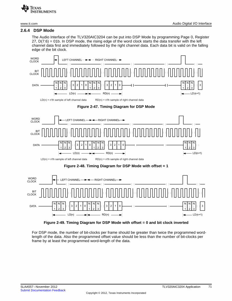
LD(n) LD(n+1)
BITCLOCK
DATAN-1
N-2
N-3
2 1 03N-1
N-2
N-3
03 2 1N-1
N-2
N-3
3
RD(n)
WORDCLOCK
LEFT CHANNEL RIGHT CHANNEL
LD(n) LD(n+1)
BITCLOCK
DATA -1
-2
-3
2 1 03 -1
-2
-3
03 2 1 -1
-2
N N N N N N N N N-3
RD(n)
WORDCLOCK
LEFT CHANNEL RIGHT CHANNEL
LD(n) = n'th sample of left channel data RD(n) = n'th sample of right channel data
LD(n) LD(n+1)
BITCLOCK
DATA -1
-2
-3
2 1 03 -1
-2
-3
03 2 1 -1
-2
N N N N N N N N N-3
3
RD(n)
WORDCLOCK
LEFT CHANNEL RIGHT CHANNEL
LD(n) = n'th sample of left channel data RD(n) = n'th sample of right channel data
www.ti.com Audio Digital I/O Interface
2.6.4 DSP Mode
The Audio Interface of the TLV320AIC3204 can be put into DSP Mode by programming Page 0, Register27, D(7:6) = 01b. In DSP mode, the rising edge of the word clock starts the data transfer with the leftchannel data first and immediately followed by the right channel data. Each data bit is valid on the fallingedge of the bit clock.
Figure 2-47. Timing Diagram for DSP Mode
Figure 2-48. Timing Diagram for DSP Mode with offset = 1
Figure 2-49. Timing Diagram for DSP Mode with offset = 0 and bit clock inverted
For DSP mode, the number of bit-clocks per frame should be greater than twice the programmed word-length of the data. Also the programmed offset value should be less than the number of bit-clocks perframe by at least the programmed word-length of the data.
71SLAA557–November 2012 TLV320AIC3204 ApplicationSubmit Documentation Feedback
Copyright © 2012, Texas Instruments Incorporated

BCLK
WCLK
DOUT
DOUT_int
S_DIN
BCLK
DIN
WCLK
DIN
DOUT
Primary
Audio
Processor
S_WCLK
DAC_FS
ADC_FS
S_BCLK
BCLK_OUT
BCLK
S_BCLK
WCLK
S_WCLK
DIN
S_DIN
WCLK
ADC_WCLK
Audio
Digital
Serial
Interface
BCLK_INT
DAC_WCLK_INT
ADC_WCLK_INT
DIN_INT
GPIO
SCLK
MISO
S_BCLK
DOUT
BCLK
BCLK_OUT
GPIO
SCLK
MISO
S_WCLK
DOUT
WCLK
DAC_FS
ADC_FS
GPIO
SCLK
S_DIN
DOUT_int
DIN
MISO
(S_DOUT)
Clock
Generation
BCLK_OUT
DAC_FS
ADC_FSWCLK
DIN
DOUT
Secondary
Audio
Processor
BCLK
GPIO
SCLK
MISO
ADC_FS
ADC_WCLK
BCLK2
WCLK2
Audio Digital I/O Interface www.ti.com
2.6.5 Secondary I2S
The audio serial interface on the TLV320AIC3204 has an extensive IO control to allow communicationwith two independent processors for audio data. Each processor can communicate with the device one ata time. This feature is enabled by register programming of the various pin selections.
Figure 2-50. Audio Serial Interface Multiplexing
The secondary audio interface uses multifunction pins. For an overview on multifunction pins please seeSection 2.1.3. Figure 2-50 illustrates possible audio interface routing. The multifunction pins SCLK andMISO are only available in I2C communication mode.
This multiplexing capability allows the TLV320AIC3204 to communicate with two separate devices withindependent I2S or PCM busses, one at a time.
72 TLV320AIC3204 Application SLAA557–November 2012Submit Documentation Feedback
Copyright © 2012, Texas Instruments Incorporated

www.ti.com Clock Generation and PLL
2.7 Clock Generation and PLL
The TLV320AIC3204 supports a wide range of options for generating clocks for the ADC and DACsections as well as interface and other control blocks. The clocks for ADC and DAC require a sourcereference clock. This clock can be provided on variety of device pins such as MCLK, BCLK or GPI pins.The CODEC_CLKIN can then be routed through highly-flexible clock dividers to generate the variousclocks required for the ADC and DAC sections. In the event that the desired audio clocks cannot begenerated from the reference clocks on MCLK, BCLK or GPIO, the TLV320AIC3204 also provides theoption of using the on-chip PLL which supports a wide range of fractional multiplication values to generatethe required clocks. Starting from CODEC_CLKIN the TLV320AIC3204 provides several programmableclock dividers to help achieve a variety of sampling rates for ADC, DAC and clocks for the processingblock.
To minimize power consumption, the system ideally provides a master clock that is a suitable integermultiple of the desired sampling frequencies. In such cases, internal dividers can be programmed to setup the required internal clock signals at very low power consumption. For cases where such master clocksare not available, the built-in PLL can be used to generate a clock signal that serves as an internal masterclock. In fact, this master clock can also be routed to an output pin and may be used elsewhere in thesystem. The clock system is flexible enough that it even allows the internal clocks to be derived directlyfrom an external clock source, while the PLL is used to generate some other clock that is only usedoutside the TLV320AIC3204.
73SLAA557–November 2012 TLV320AIC3204 ApplicationSubmit Documentation Feedback
Copyright © 2012, Texas Instruments Incorporated

MDACNDAC
CLKIN_CODECCLK_MOD_DAC
´
=
DOSRMDACNDAC
CLKIN_CODEC
´´
fS_DAC =
MADCNADC
CLKIN_CODECCLK_MOD_ADC
´
=
AOSRMADCNADC
CLKIN_CODECfS_ADC
´´
=
PLL_CLKIN
MCLK
BCLK
GPIO
DIN/MFP1
MCLK
BCLK
GPIO
÷NDAC
÷MDAC
÷DOSR
PLLx(RxJ·D)/P
PLL_CLK
CODEC_CLKIN
÷NADCNDAC = 1,2,....,127,128 NADC = 1,2,....,127,128
DAC_CLK ADC_CLK
MDAC = 1,2,...,127,128 ÷MADC MADC = 1,2,...,127,128
ADC_MOD_CLKDAC_MOD_CLK
÷AOSRDOSR = 1,2,...,1023,1024 AOSR = 1,2,...,255,256
DAC_FS ADC_FS
Clock Generation and PLL www.ti.com
Figure 2-51. Clock Distribution Tree
(14)
(15)
(16)
(17)
Table 2-24. CODEC CLKIN Clock Dividers
Divider Bits
NDAC Page 0, Register 11, D(6:0)
MDAC Page 0, Register 12, D(6:0)
DOSR Page 0, Register 13, D(1:0) + Page 0, Register 14, D(7:0)
74 TLV320AIC3204 Application SLAA557–November 2012Submit Documentation Feedback
Copyright © 2012, Texas Instruments Incorporated

÷N
BCLK
DAC_CLK
ADC_MOD_CLKDAC_MOD_CLK
ADC_CLK
BDIV_CLKIN
N = 1,2,...,127,128
www.ti.com Clock Generation and PLL
Table 2-24. CODEC CLKIN Clock Dividers (continued)
Divider Bits
NADC Page 0, Register 18, D(6:0)
MADC Page 0, Register 19, D(6:0)
AOSR Page 0, Register 20, D(7:0)
The DAC Modulator is clocked by DAC_MOD_CLK. For proper power-up of the DAC Channel, theseclocks must be enabled by configuring the NDAC and MDAC clock dividers ( Page 0,Register 11, D(7) = 1and Page 0, Register 12, D(7) = 1). When the DAC channel is powered down, the device internallyinitiates a power-down sequence for proper shut-down. During this shut-down sequence, the NDAC andMDAC dividers must not be powered down, or else a proper low power shut-down may not take place.The user can read the power-status flag in Page 0, Register 37, D(7) and Page 0, Register 37, D(3).When both flags indicate power-down, the MDAC divider may be powered down, followed by the NDACdivider.
The ADC modulator is clocked by ADC_MOD_CLK. For proper power-up of the ADC Channel, theseclocks are enabled by the NADC and MADC clock dividers (Page 0,Register 18, D(7) = 1 and Page 0,Register 19, D(7) = 1). When the ADC channel is powered down, the device internally initiates a power-down sequence for proper shut-down. During this shut-down sequence, the NADC and MADC dividersmust not be powered down, or else a proper low power shut-down may not take place. The user can readthe power-status flag in Page 0, Register 36, D(6) and Page 0, Register 36, D(2). When both flagsindicate power-down, the MADC divider may be powered down, followed by NADC divider.
When ADC_CLK is derived from the NDAC divider output, the NDAC must be kept powered up till thepower-down status flags for ADC do not indicate power-down. When the input to the AOSR clock divideris derived from DAC_MOD_CLK, then MDAC must be powered up when ADC_FS is needed ( such aswhen WCLK is generated by TLV320AIC3204 or AGC is enabled) and can be powered down only afterthe ADC power-down flags indicate power-down status.
In general, all the root clock dividers should be powered down only after the child clock dividers have beenpowered down for proper operation.
The TLV320AIC3204 also has options for routing some of the internal clocks to the output pins of thedevice to be used as general purpose clocks in the system. The feature is shown in Figure 2-52.
Figure 2-52. BCLK Output Options
75SLAA557–November 2012 TLV320AIC3204 ApplicationSubmit Documentation Feedback
Copyright © 2012, Texas Instruments Incorporated

÷M
CLKOUT
CDIV_CLKIN
MCLK BCLK DIN
GPIO MISO DOUT
PLL_CLK
DAC_CLK ADC_CLK
DAC_MOD_CLK ADC_MOD_CLK
M = 1,2,...,127,128
Clock Generation and PLL www.ti.com
In the mode when TLV320AIC3204 is configured to drive the BCLK pin (Page 0, Register 27, D(3) = ’1’) itcan be driven as divided value of BDIV_CLKIN. The division value can be programmed in Page 0,Register 30, D(6:0) from 1 to 128. The BDIV_CLKIN can itself be configured to be one of DAC_CLK,DAC_MOD_CLK, ADC_CLK or ADC_MOD_CLK by configuring the BDIV_CLKIN mux in Page 0, Register29, D(1:0). Additionally a general purpose clock can be driven out on either GPIO, DOUT or MISO pin.This clock can be a divided-down version of CDIV_CLKIN. The value of this clock divider can beprogrammed from 1 to 128 by writing to Page 0, Register 26, D(6:0). The CDIV_CLKIN can itself beprogrammed as one of the clocks among the list shown in Figure 2-53. This configuration is available byprogramming the mux in Page 0, Register 25, D(2:0).
Figure 2-53. General Purpose Clock Output Options
Table 2-25. Maximum TLV320AIC3204 Clock Frequencies
DVdd ≥ 1.26V DVdd ≥ 1.65V
CODEC_CLKIN 50MHz 137MHz when NDAC is even, NADC is even112MHz when NDAC is even, NADC is odd110MHz when NDAC is odd, NADC is even110MHz when NDAC is odd, NADC is odd
ADC_CLK 25MHz 55.296MHz
ADC_MOD_CLK 6.758MHz 6.758MHz
ADC_FS 0.192MHz 0.192MHz
DAC_CLK 25MHz 55.296MHz
DAC_MOD_CLK 6.758MHz 6.758MHz4.2MHz when Class-D Mode Headphone
is used
DAC_FS 0.192MHz 0.192MHz
BDIV_CLKIN 25MHz 55.296MHz
CDIV_CLKIN 50MHz 112MHz when M is odd137MHz when M is even
76 TLV320AIC3204 Application SLAA557–November 2012Submit Documentation Feedback
Copyright © 2012, Texas Instruments Incorporated
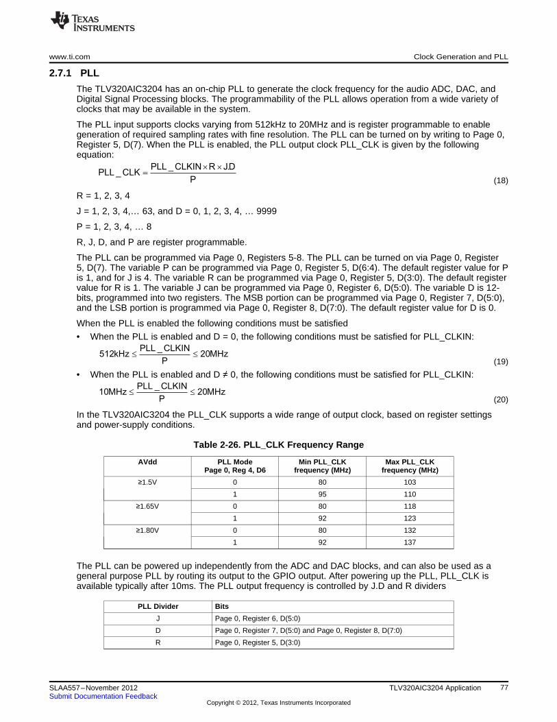
MHz20P
CLKIN_PLLMHz10 ££
MHz20P
CLKIN_PLLkHz512 ££
PLL _ CLKIN R J.DPLL _ CLK
P
´ ´
=
www.ti.com Clock Generation and PLL
2.7.1 PLL
The TLV320AIC3204 has an on-chip PLL to generate the clock frequency for the audio ADC, DAC, andDigital Signal Processing blocks. The programmability of the PLL allows operation from a wide variety ofclocks that may be available in the system.
The PLL input supports clocks varying from 512kHz to 20MHz and is register programmable to enablegeneration of required sampling rates with fine resolution. The PLL can be turned on by writing to Page 0,Register 5, D(7). When the PLL is enabled, the PLL output clock PLL_CLK is given by the followingequation:
(18)
R = 1, 2, 3, 4
J = 1, 2, 3, 4,… 63, and D = 0, 1, 2, 3, 4, … 9999
P = 1, 2, 3, 4, … 8
R, J, D, and P are register programmable.
The PLL can be programmed via Page 0, Registers 5-8. The PLL can be turned on via Page 0, Register5, D(7). The variable P can be programmed via Page 0, Register 5, D(6:4). The default register value for Pis 1, and for J is 4. The variable R can be programmed via Page 0, Register 5, D(3:0). The default registervalue for R is 1. The variable J can be programmed via Page 0, Register 6, D(5:0). The variable D is 12-bits, programmed into two registers. The MSB portion can be programmed via Page 0, Register 7, D(5:0),and the LSB portion is programmed via Page 0, Register 8, D(7:0). The default register value for D is 0.
When the PLL is enabled the following conditions must be satisfied
• When the PLL is enabled and D = 0, the following conditions must be satisfied for PLL_CLKIN:
(19)
• When the PLL is enabled and D ≠ 0, the following conditions must be satisfied for PLL_CLKIN:
(20)
In the TLV320AIC3204 the PLL_CLK supports a wide range of output clock, based on register settingsand power-supply conditions.
Table 2-26. PLL_CLK Frequency Range
AVdd PLL Mode Min PLL_CLK Max PLL_CLKPage 0, Reg 4, D6 frequency (MHz) frequency (MHz)
≥1.5V 0 80 103
1 95 110
≥1.65V 0 80 118
1 92 123
≥1.80V 0 80 132
1 92 137
The PLL can be powered up independently from the ADC and DAC blocks, and can also be used as ageneral purpose PLL by routing its output to the GPIO output. After powering up the PLL, PLL_CLK isavailable typically after 10ms. The PLL output frequency is controlled by J.D and R dividers
PLL Divider Bits
J Page 0, Register 6, D(5:0)
D Page 0, Register 7, D(5:0) and Page 0, Register 8, D(7:0)
R Page 0, Register 5, D(3:0)
77SLAA557–November 2012 TLV320AIC3204 ApplicationSubmit Documentation Feedback
Copyright © 2012, Texas Instruments Incorporated
Control Interfaces www.ti.com
The D-divider value is 14-bits wide and is controlled by 2 registers. For proper update of the D-dividervalue, Page 0, Register 7 must be programmed first followed immediately by Page 0, Register 8. Unlessthe write to Page 0, Register 8 is completed, the new value of D will not take effect.
The clocks for codec and various signal processing blocks, CODEC_CLKIN can be generated from MCLKinput, BCLK input, GPIO input or PLL_CLK (Page 0, Register 4, D(1:0)).
If the CODEC_CLKIN is derived from the PLL, then the PLL must be powered up first and powered downlast.
Table 2-27 lists several example cases of typical MCLK rates and how to program the PLL to achieve asample rate fS of either 44.1kHz or 48kHz.
Table 2-27. PLL Example Configurations
fS = 44.1kHz
MCLK (MHz) PLLP PLLR PLLJ PLLD MADC NADC AOSR MDAC NDAC DOSR
2.8224 1 3 10 0 3 5 128 3 5 128
5.6448 1 3 5 0 3 5 128 3 5 128
12 1 1 7 560 3 5 128 3 5 128
13 1 2 4 2336 13 3 64 4 6 104
16 1 1 5 2920 3 5 128 3 5 128
19.2 1 1 4 4100 3 5 128 3 5 128
48 4 1 7 560 3 5 128 3 5 128
fS = 48kHz
2.048 1 3 14 0 2 7 128 7 2 128
3.072 1 4 7 0 2 7 128 7 2 128
4.096 1 3 7 0 2 7 128 7 2 128
6.144 1 2 7 0 2 7 128 7 2 128
8.192 1 4 3 0 2 8 128 4 4 128
12 1 1 7 1680 2 7 128 7 2 128
16 1 1 5 3760 2 7 128 7 2 128
19.2 1 1 4 4800 2 7 128 7 2 128
48 4 1 7 1680 2 7 128 7 2 128
2.8 Control Interfaces
The TLV320AIC3204 control interface supports SPI or I2C communication protocols, with the protocolselectable using the SPI_SELECT pin. For SPI, SPI_SELECT should be tied high; for I2C, SPI_SELECTshould be tied low. Changing the state of SPI_SELECT during device operation is not recommended.
2.8.1 I2C Control Mode
The TLV320AIC3204 supports the I2C control protocol, and will respond to the I2C address of 0011000.I2C is a two-wire, open-drain interface supporting multiple devices and masters on a single bus. Deviceson the I2C bus only drive the bus lines LOW by connecting them to ground; they never drive the bus linesHIGH. Instead, the bus wires are pulled HIGH by pullup resistors, so the bus wires are HIGH when nodevice is driving them LOW. This circuit prevents two devices from conflicting; if two devices drive the bussimultaneously, there is no driver contention.
Communication on the I2C bus always takes place between two devices, one acting as the master and theother acting as the slave. Both masters and slaves can read and write, but slaves can only do so underthe direction of the master. Some I2C devices can act as masters or slaves, but the TLV320AIC3204 canonly act as a slave device.
An I2C bus consists of two lines, SDA and SCL. SDA carries data, and the SCL signal provides the clock.All data is transmitted across the I2C bus in groups of eight bits. To send a bit on the I2C bus, the SDA lineis driven to the appropriate level while SCL is LOW (a LOW on SDA indicates the bit is zero, while a HIGHindicates the bit is one).
78 TLV320AIC3204 Application SLAA557–November 2012Submit Documentation Feedback
Copyright © 2012, Texas Instruments Incorporated

Start
(M)7-bit Device Address
(M)
Write
(M)
Slave
Ack
(S)
8-bit Register Address
(M)
Slave
Ack
(S)
SDA
SCL
7-bit Device Address
(M)
Read
(M)
Slave
Ack
(S)
DA(6) DA(0) RA(7) RA(0) DA(6) DA(0) D(7) D(0)
8-bit Register Data
(S)
Stop
(M)
Master
No Ack
(M)
Repeat
Start
(M)
(M) => SDA Controlled by Master
(S) => SDA Controlled by Slave
DA(6) DA(0) RA(7) RA(0) D(7) D(0)
Start
(M)
7-bit Device Address
(M)
Write
(M)
Slave
Ack
(S)
8-bit Register Address
(M)
Slave
Ack
(S)
8-bit Register Data
(M)
Stop
(M)
Slave
Ack
(S)
SDA
SCL
(M) => SDA Controlled by Master
(S) => SDA Controlled by Slave
www.ti.com Control Interfaces
Once the SDA line has settled, the SCL line is brought HIGH, then LOW. This pulse on the SCL lineclocks the SDA bit into the receiver’s shift register.
The I2C bus is bidirectional: the SDA line is used both for transmitting and receiving data. When a masterreads from a slave, the slave drives the data line; when a master sends to a slave, the master drives thedata line.
Most of the time the bus is idle, no communication is taking place, and both lines are HIGH. Whencommunication is taking place, the bus is active. Only master devices can start communication on the bus.Normally, the data line is only allowed to change state while the clock line is LOW. If the data line changesstate while the clock line is HIGH, it is either a START condition or its counterpart, a STOP condition. ASTART condition is when the clock line is HIGH and the data line goes from HIGH to LOW. A STOPcondition is when the clock line is HIGH and the data line goes from LOW to HIGH.
After the master issues a START condition, it sends a byte that selects the slave device forcommunication. This byte is called the address byte. Each device on an I2C bus has a unique 7-bitaddress to which it responds. (Slaves can also have 10-bit addresses; see the I2C specification fordetails.) The master sends an address in the address byte, together with a bit that indicates whether itwishes to read from or write to the slave device.
Every byte transmitted on the I2C bus, whether it is address or data, is acknowledged with anacknowledge bit. When a master has finished sending a byte (eight data bits) to a slave, it stops drivingSDA and waits for the slave to acknowledge the byte. The slave acknowledges the byte by pulling SDALOW. The master then sends a clock pulse to clock the acknowledge bit. Similarly, when a master hasfinished reading a byte, it pulls SDA LOW to acknowledge this to the slave. The master then sends a clockpulse to clock the bit. (Remember that the master always drives the clock line.)
A not-acknowledge is performed by simply leaving SDA HIGH during an acknowledge cycle. If a device isnot present on the bus, and the master attempts to address it, it will receive a not−acknowledge becauseno device is present at that address to pull the line LOW.
When a master has finished communicating with a slave, it may issue a STOP condition. When a STOPcondition is issued, the bus becomes idle again. A master may also issue another START condition. Whena START condition is issued while the bus is active, it is called a repeated START condition.
The TLV320AIC3204 can also respond to and acknowledge a General Call, which consists of the masterissuing a command with a slave address byte of 00H. This feature is disabled by default, but can beenabled via Page 0, Register 34, Bit D(5).
Figure 2-54. I2C Write
Figure 2-55. I2C Read
79SLAA557–November 2012 TLV320AIC3204 ApplicationSubmit Documentation Feedback
Copyright © 2012, Texas Instruments Incorporated

RA(6) RA(5) RA(0) D(7) D(6) D(0)
7-bit Register Address Write 8-bit Register Data
SS
SCLK
MOSI
MISO
Hi-Z Hi-Z
Hi-Z Hi-Z
Control Interfaces www.ti.com
In the case of an I2C register write, if the master does not issue a STOP condition, then the device entersauto-increment mode. So in the next eight clocks, the data on SDA is treated as data for the nextincremental register.
Similarly, in the case of an I2C register read, after the device has sent out the 8-bit data from theaddressed register, if the master issues a ACKNOWLEDGE, the slave takes over control of SDA bus andtransmit for the next 8 clocks the data of the next incremental register.
2.8.2 SPI Digital Interface
In the SPI control mode, the TLV320AIC3204 uses the pins SCL/SS as SS, SCLK as SCLK, MISO asMISO, SDA/MOSI as MOSI; a standard SPI port with clock polarity setting of 0 (typical microprocessorSPI control bit CPOL = 0). The SPI port allows full-duplex, synchronous, serial communication between ahost processor (the master) and peripheral devices (slaves). The SPI master (in this case, the hostprocessor) generates the synchronizing clock (driven onto SCLK) and initiates transmissions. The SPIslave devices (such as the TLV320AIC3204) depend on a master to start and synchronize transmissions.A transmission begins when initiated by an SPI master. The byte from the SPI master begins shifting in onthe slave MOSI pin under the control of the master serial clock (driven onto SCLK). As the byte shifts inon the MOSI pin, a byte shifts out on the MISO pin to the master shift register.
The TLV320AIC3204 interface is designed so that with a clock-phase bit setting of 1 (typicalmicroprocessor SPI control bit CPHA = 1), the master begins driving its MOSI pin and the slave beginsdriving its MISO pin on the first serial clock edge. The SSZ pin can remain low between transmissions;however, the TLV320AIC3204 only interprets the first 8 bits transmitted after the falling edge of SSZ as acommand byte, and the next 8 bits as a data byte only if writing to a register. Reserved register bitsshould be written to their default values. The TLV320AIC3204 is entirely controlled by registers. Readingand writing these registers is accomplished by an 8-bit command sent to the MOSI pin of the part prior tothe data for that register. The command is structured as shown in Table 2-28. The first 7 bits specify theregister address which is being written or read, from 0 to 127 (decimal). The command word ends with anR/W bit, which specifies the direction of data flow on the serial bus. In the case of a register write, the R/Wbit should be set to 0. A second byte of data is sent to the MOSI pin and contains the data to be written tothe register. Reading of registers is accomplished in similar fashion. The 8-bit command word sends the 7-bit register address, followed by R/W bit = 1 to signify a register read is occurring. The 8-bit register datais then clocked out of the part on the MISO pin during the second 8 SCLK clocks in the frame.
Table 2-28. SPI Command Word
Bit 7 Bit 6 Bit 5 Bit 4 Bit 3 Bit 2 Bit 1 Bit 0
ADDR(6) ADDR(5) ADDR(4) ADDR(3) ADDR(2) ADDR(1) ADDR(0) R/WZ
Figure 2-56. SPI Timing Diagram for Register Write
80 TLV320AIC3204 Application SLAA557–November 2012Submit Documentation Feedback
Copyright © 2012, Texas Instruments Incorporated
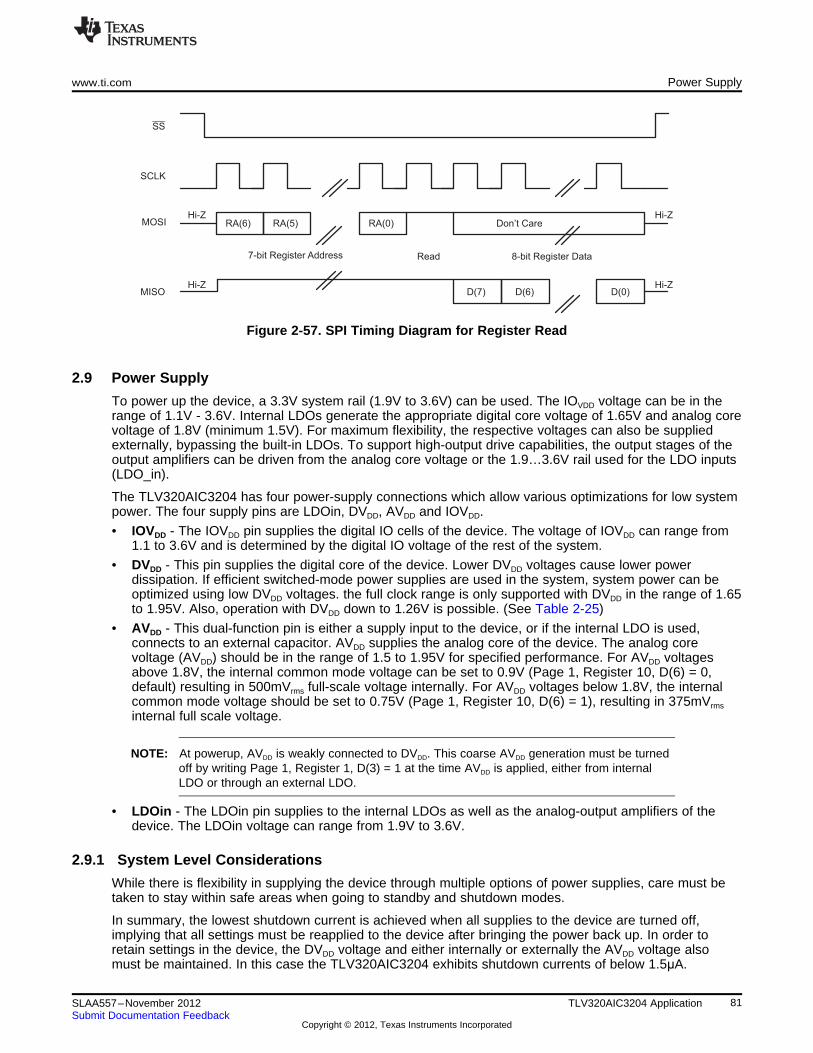
RA(6) RA(5) RA(0) Don’t Care
7-bit Register Address Read 8-bit Register Data
SS
SCLK
MOSI
MISO
Hi-Z Hi-Z
D(7) D(6) D(0)Hi-Z Hi-Z
www.ti.com Power Supply
Figure 2-57. SPI Timing Diagram for Register Read
2.9 Power Supply
To power up the device, a 3.3V system rail (1.9V to 3.6V) can be used. The IOVDD voltage can be in therange of 1.1V - 3.6V. Internal LDOs generate the appropriate digital core voltage of 1.65V and analog corevoltage of 1.8V (minimum 1.5V). For maximum flexibility, the respective voltages can also be suppliedexternally, bypassing the built-in LDOs. To support high-output drive capabilities, the output stages of theoutput amplifiers can be driven from the analog core voltage or the 1.9…3.6V rail used for the LDO inputs(LDO_in).
The TLV320AIC3204 has four power-supply connections which allow various optimizations for low systempower. The four supply pins are LDOin, DVDD, AVDD and IOVDD.
• IOVDD - The IOVDD pin supplies the digital IO cells of the device. The voltage of IOVDD can range from1.1 to 3.6V and is determined by the digital IO voltage of the rest of the system.
• DVDD - This pin supplies the digital core of the device. Lower DVDD voltages cause lower powerdissipation. If efficient switched-mode power supplies are used in the system, system power can beoptimized using low DVDD voltages. the full clock range is only supported with DVDD in the range of 1.65to 1.95V. Also, operation with DVDD down to 1.26V is possible. (See Table 2-25)
• AVDD - This dual-function pin is either a supply input to the device, or if the internal LDO is used,connects to an external capacitor. AVDD supplies the analog core of the device. The analog corevoltage (AVDD) should be in the range of 1.5 to 1.95V for specified performance. For AVDD voltagesabove 1.8V, the internal common mode voltage can be set to 0.9V (Page 1, Register 10, D(6) = 0,default) resulting in 500mVrms full-scale voltage internally. For AVDD voltages below 1.8V, the internalcommon mode voltage should be set to 0.75V (Page 1, Register 10, D(6) = 1), resulting in 375mVrms
internal full scale voltage.
NOTE: At powerup, AVDD is weakly connected to DVDD. This coarse AVDD generation must be turnedoff by writing Page 1, Register 1, D(3) = 1 at the time AVDD is applied, either from internalLDO or through an external LDO.
• LDOin - The LDOin pin supplies to the internal LDOs as well as the analog-output amplifiers of thedevice. The LDOin voltage can range from 1.9V to 3.6V.
2.9.1 System Level Considerations
While there is flexibility in supplying the device through multiple options of power supplies, care must betaken to stay within safe areas when going to standby and shutdown modes.
In summary, the lowest shutdown current is achieved when all supplies to the device are turned off,implying that all settings must be reapplied to the device after bringing the power back up. In order toretain settings in the device, the DVDD voltage and either internally or externally the AVDD voltage alsomust be maintained. In this case the TLV320AIC3204 exhibits shutdown currents of below 1.5μA.
81SLAA557–November 2012 TLV320AIC3204 ApplicationSubmit Documentation Feedback
Copyright © 2012, Texas Instruments Incorporated

Power Supply www.ti.com
2.9.1.1 Supply From Single Voltage Rail (1.9 to 3.6V)
The device can be powered directly from a single 3.3V rail through the LDOin pin. During operation theDVDD LDO is activated via the LDO_select pin, and the AVDD LDO is activated via control registers (Page1, Register 2, D(0) = 1).
2.9.1.1.1 Standby Mode (3.3V operation)
To put the device in standby mode, the AVDD and DVDD LDOs as well as the Reference Block (Page 1,Register 123, D(2:0) = 101) must stay on, and all other blocks powered down. This state results in astandby current of approximately 180mA. In standby mode, the device responds quickly to playbackrequests.
2.9.1.1.2 Sleep Mode (3.3V operation)
In this mode all settings and memory content of the device are retained. To put the device into sleepmode, the DVDD LDO must remain powered up (LDO_select pin), the AVDD LDO must be powered down(Page 1, Register 2, D(0) = 0), the crude AVDD generation must be turned on (Page 1, Register 1, D(3) =0) and the analog blocks must be powered down (Page 1, Register 2, D(3) = 1). The sleep-mode powerconsumption is approximately 50mA
2.9.1.1.3 Shutdown Mode
To shutdown the device, the external supply can be turned off completely.
2.9.1.2 Supply From Single Voltage Rail (1.8V).
If a single 1.8V rail is used, generating the 1.8V from a higher battery voltage via a DC-DC converterresults in good system-level efficiency. In this setup, the headphone output voltage is limited to 500mVrms,and the maximum headphone output power is 15mW into 16Ω.
The 1.8V rail connected to the DVDD pin can also be connected to the AVDD pin. The device operates withthis connection, but the achievable performance is a function of the voltage ripple typically found on DC-DC converter outputs. To achieve specified performance, an external low-input-voltage 1.6V LDO must beconnected between the 1.8V rail and the AVDD input.
During operation, the AVDD LDO is deactivated via control register Page 1, Register 2, D(0) = 0. In thiscase the LDOin pin should be connected to DVDD.
2.9.1.2.1 Standby Mode (1.8V operation)
To put the device in standby mode, both external voltages (AVDD and DVDD) and the reference block insidethe TLV320AIC3204 must stay on (Page 1, Register 123, D(2:0) = 101), all other blocks should bepowered down. This state results in standby current of approximately 100μA from the AVDD supply.
In standby mode the device responds very quickly to playback requests.
2.9.1.2.2 Sleep Mode (1.8V operation)
In this mode, all settings and memory content of the device is retained. To put the device into sleep mode,the external DVDD must remain powered up, the external AVDD LDO must be powered down, the crudeAVdd generation must be turned on (Page 1, Register 1, D(3) = 0) and the analog blocks must bepowered down (Page 1, Register 2, D(3) = 1). The device's sleep mode power consumption in this case is< 1.5μA
2.9.1.2.3 Shutdown Mode
To shut down the device, the external supplies can be turned off completely. If the 1.8V rail cannot beturned off, the crude AVDD generation must be turned on (Page 1, Register 1, D(3) = 0) and the analogblocks must be powered down (Page 1, Register 2, D(3) = 1). This state results in a device shutdowncurrent < 1.5μA.
82 TLV320AIC3204 Application SLAA557–November 2012Submit Documentation Feedback
Copyright © 2012, Texas Instruments Incorporated

s
g
s
m
1 3
Micbias
m
s
g
s
MICBIAS
HPR
HPL
SCLK
Micpga
www.ti.com Reference Voltage
2.9.1.3 Other Supply Options
There are other options to power the device. Apply the following rules:
• During normal operation all supply pins must be connected to a supply (via internal LDO or external).
• Whenever the LDOin supply is present,
– The DVDD supply must be present as well
– If the AVDD supply is not present, then the crude internal AVDD generation must be turned on (Page1, Register 1, D(3) = 0)
• Whenever the DVdd supply is on, and either AVDD or LDOin or both supplies are off, the analog blocksmust be powered down (Page 1, Register 2, D(3) = 1)
2.10 Reference Voltage
All data converters require a DC reference voltage. The TLV320AIC3204 achieves its low-noiseperformance by internally generating a low-noise reference voltage. This reference voltage is generatedusing a band-gap circuit with a good PSRR performance. This reference voltage must be filteredexternally using a minimum 1μF capacitor connected from the REF pin to analog ground (AVSS).
To achieve low power consumption, this reference block is powered down when all analog blocks insidethe device are powered down. In this condition, the REF pin is 3-stated. On powerup of any analog block,the reference block also powers up and the REF pin settles to its steady-state voltage after the settlingtime (a function of the decoupling capacitor on the REF pin). This time is approximately 1 second whenusing a 1μF decoupling capacitor. In the event that a faster power-up is required, the reference block canbe kept powered up (even when no other analog block is powered up) by programming Page 1, Register123, D(2) = 1. However, in this case, an additional 125μA of current from AVDD is consumed. Additionally,to achieve a faster powerup, a fast-charge option is also provided where the charging time can becontrolled between 40ms and 120ms by programming Page 1, Register 123, D(1:0). By default, the fastcharge option is disabled.
2.11 Device Special Functions
2.11.1 Headset Detection
The TLV320AIC3204 includes extensive capability to monitor a headphone, microphone, or headset jack,to determine if a plug has been inserted into the jack, and then determine what type of headset is wired tothe plug. The device also includes the capability to detect a button press, even, for example, when startingcalls on mobile phones with headsets. This feature is available while using I2C protocol for controlinterface. The figure shows the circuit configuration to enable this feature.
Figure 2-58. Jack Connections for Headset Detection
83SLAA557–November 2012 TLV320AIC3204 ApplicationSubmit Documentation Feedback
Copyright © 2012, Texas Instruments Incorporated

Device Special Functions www.ti.com
This feature is enabled by programming Page 0, Register 67, D(1). In order to avoid false detections dueto mechanical vibrations in headset jacks or microphone buttons, a debounce function is provided forglitch rejection. For the case of headset insertion, a debounce function with a range of 32ms - 512ms isprovided. This function can be programmed via Page 0, Register 67, D(4:2). For improved button-pressdetection, the debounce function has a range of 8ms to 32ms by programming Page 0, Register 67,D(1:0).
The TLV320AIC3204 also provides feedback to user when a button press, or a headset insertion orremoval event is detected through register readable flags as well as an interrupt on the IO pins. The valuein Page 0, Register 46, D(5:4) provides the instantaneous state of button press and headset insertion.Page 0, Register 44, D(5) is a sticky (latched) flag that is set when the button-press event is detected.Page 0, Register 44, D(4) is a sticky flag which is set when the headset insertion or removal event isdetected. These sticky flags are set by the event occurrence, and are reset only when read, requiring thesoftware to poll Page 0, Register 44. To avoid polling and the associated overhead, the TLV320AIC3204also provides an interrupt feature where the events can trigger the INT1 and-or INT2 interrupts. Theseinterrupt events can be routed to one of the digital output pins. Please see Section 2.11.2 for details.
The TLV320AIC3204 not only detects a headset insertion event, but also is able to distinguish betweenthe different headsets inserted such as stereo headphones or cellular headphones. After the headset-detection event, the user can read Page 0, Register 67, D(6:5) to determine the type of headset inserted.
Table 2-29. Headset Detection Block Registers
Register Description
Page 0, Register 67, D(1) Headset Detection Enable or Disable
Page 0, Register 67, D(4:2) Debounce Programmability for Headset Detection
Page 0, Register 67, D(1:0) Debounce Programmability for Button Press
Page 0, Register 44, D(5) Sticky Flag for Button Press Event
Page 0, Register 44, D(4) Sticky Flag for Headset Insertion or Removal Event
Page 0, Register 46, D(5) Status Flag for Button Press Event
Page 0, Register 46, D(4) Status Flag for Headset Insertion and Removal
Page 0, Register 67, D(6:5) Flags for type of Headset Detected
The headset detection block requires AVdd to be powered and Master Analog Power control in Page 1,Register 2, D(3) to be enabled. The headset detection feature in the TLV320AIC3204 is achieved with avery low power overhead, requiring less than 20μA of additional current from the AVdd supply.
2.11.2 Interrupts
Some specific events in the TLV320AIC3204 which may require host processor intervention, can be usedto trigger interrupts to the host processor. INterrupt use avoids polling the status-flag registerscontinuously. The TLV320AIC3204 has two defined interrupts; INT1 and INT2 that can be configured byprogramming Page 0, Register 48 and 49. A user can configure the interrupts INT1 and INT2 to betriggered by one or many events such as
• Headset Detection
• Button Press
• DAC DRC Signal exceeding Threshold
• Noise detected by AGC
• Over-current condition in headphones
• Data Overflow in ADC and DAC Processing Blocks and Filters
Each of these INT1 and INT2 interrupts can be routed to output pins like GPIO, DOUT and MISO byconfiguring the respective output control registers in Page 0, Register 52, 53 and 55. These interruptsignals can either be configured as a single pulse or a series of pulses by programming Page 0, Register48, D(0) and Page 0, Register 49, D(0). If the user configures the interrupts as a series of pulses, theevents will trigger the start of pulses that will stop when the flag registers in Page 0, Register 42, 44 and45 are read by the user to determine the cause of the interrupt.
84 TLV320AIC3204 Application SLAA557–November 2012Submit Documentation Feedback
Copyright © 2012, Texas Instruments Incorporated

Chapter 3SLAA557–November 2012
Device Initialization
The requirements of the application circuit determine device setup details such as clock generation, powersources, references voltage,and special functions that may add value to the end application. Exampledevice setups are described in the final section.
Topic ........................................................................................................................... Page
3.1 Reset ............................................................................................................... 863.2 Device Startup Lockout Times ............................................................................ 863.3 Analog and Reference Startup ............................................................................ 863.4 PLL Startup ...................................................................................................... 863.5 Setting Device Common Mode Voltage ................................................................ 86
85SLAA557–November 2012 Device InitializationSubmit Documentation Feedback
Copyright © 2012, Texas Instruments Incorporated

Reset www.ti.com
3.1 Reset
The TLV320AIC3204 internal logic must be initialized to a known condition for proper device function. Toinitialize the device to the default operation condition, the hardware reset pin (RESET) must be pulled lowfor at least 10ns. For this initialization to work, both the IOVDD and DVDD supplies must be powered up.While the TLV320AIC3204 supplies are powering up, pull the RESET pin low. To allow hardware resetcontrol independent of system power supply, drive the RESET pin through a GPIO terminal from the hostprocessor. While the device requires a hardware reset after the power supplies are powered up,subsequently the device can be reset via software reset. Writing ‘1’ into Page 0, Register 1, D(0) resetsthe device. After a device reset, all registers are initialized with default values as listed in the Register Mapsection.
3.2 Device Startup Lockout Times
After the TLV320AIC3204 initializes through hardware reset at power-up or software reset, the internalregisters initialize to default values. This initialization takes place within 1ms after pulling the RESETsignal high. During this initialization phase, no register-read or register-write operation should beperformed on ADC or DAC coefficient buffers. Also, no block within the codec should be powered upduring the initialization phase.
3.3 Analog and Reference Startup
The TLV320AIC3204 uses an external REF pin for decoupling the reference voltage used for the dataconverters and other analog blocks. The REF pin requires a minimum 1µF decoupling capacitor from REFto AVSS. In order for any analog block to be powered up, the Analog Reference block must be powered up.By default, the Analog Reference block is implicitly powered up when any analog block is powered up, orit can be powered up independently. Detailed descriptions of Analog Reference including fast power-upoptions are provided in Section 2.10. During the time that the reference block is not completely poweredup, subsequent requests for powering up analog blocks (such as the PLL) are queued, and executed afterthe reference power up is complete.
3.4 PLL Startup
When the PLL is powered up, a startup delay of approximately 10ms is involved after the power upcommand of the PLL and before the clocks are available to the codec. This delay provides stableoperation of PLL and clock-divider logic.
3.5 Setting Device Common Mode Voltage
The TLV320AIC3204 allows the user to set the common mode voltage for analog inputs to 0.75V or 0.9Vby programming Page 1, Register 10, D(6). The input common-mode voltage of 0.9V works best when theanalog supply voltage is centered around 1.8V or above, and offers the highest possible performance. Foranalog supply voltages below 1.8V, a common mode voltage of 0.75V must be used.
Table 3-1. Input Common Mode voltage and Input Signal Swing
Input Common Mode AVdd (V) Channel Gain (dB) Single-Ended Input Differential InputVoltage (V) Swing for 0dBFS Swing for 0dBFS
output signal (VRMS) output signal (VRMS)
0.75 >1.5 –2 0.375 0.75
0.90 1.8 … 1.95 0 0.5 1.0
The choice of input common mode of 0.75V allows the use of PowerTune mode PTM_R1 which results insignificantly lower power dissipation. (see Section 2.5.1) An input common-mode voltage of 0.9V allowsthe user to maximize the signal swings and SNR.
NOTE: The input common mode setting is common for ADC record, DAC playback and AnalogBypass path
86 Device Initialization SLAA557–November 2012Submit Documentation Feedback
Copyright © 2012, Texas Instruments Incorporated

Chapter 4SLAA557–November 2012
Example Setups
The following example setups can be taken directly for the TLV320AIC3204 EVM setup.
The # marks a comment line, w marks an I2C write command followed by the device address, the I2Cregister address and the value.
4.0.1 Stereo DAC Playback with 48ksps Sample Rate and High Performance.AssumptionAVdd = 1.8V, DVdd = 1.8VMCLK = 12.288MHzExt C = 47uFBased on C the wait time will change.Wait time = N*Rpop*C + 4* Offset ramp timeDefault settings used.PLL DisabledDOSR 128
# Initialize to Page 0w 30 00 00# Initialize the device through software resetw 30 01 01# Power up the NDAC divider with value 1w 30 0b 81# Power up the MDAC divider with value 2w 30 0c 82# Program the OSR of DAC to 128w 30 0d 00w 30 0e 80# Set the word length of Audio Interface to 20bits PTM_P4w 30 1b 10# Set the DAC Mode to PRB_P8w 30 3c 08# Select Page 1w 30 00 01# Disable Internal Crude AVdd in presence of external AVdd supply or before#powering up internal AVdd LDOw 30 01 08# Enable Master Analog Power Controlw 30 02 00# Set the REF charging time to 40msw 30 7b 01# HP soft stepping settings for optimal pop performance at power up# Rpop used is 6k with N = 6 and soft step = 20usec. This should work with 47uF coupling# capacitor. Can try N=5,6 or 7 time constants as well. Trade-off delay vs “pop” sound.w 30 14 25# Set the Input Common Mode to 0.9V and Output Common Mode for Headphone to# Input Common Modew 30 0a 00# Route Left DAC to HPLw 30 0c 08# Route Right DAC to HPRw 30 0d 08# Set the DAC PTM mode to PTM_P3/4w 30 03 00w 30 04 00
87SLAA557–November 2012 Example SetupsSubmit Documentation Feedback
Copyright © 2012, Texas Instruments Incorporated

www.ti.com
# Set the HPL gain to 0dBw 30 10 00# Set the HPR gain to 0dBw 30 11 00# Power up HPL and HPR driversw 30 09 30# Wait for 2.5 sec for soft stepping to take effect# Else read Page 1, Register 63d, D(7:6). When = “11” soft-stepping is complete# Select Page 0w 30 00 00# Power up the Left and Right DAC Channels with route the Left Audio digital data to# Left Channel DAC and Right Audio digital data to Right Channel DACw 30 3f d6# Unmute the DAC digital volume controlw 30 40 00
4.0.2 Stereo DAC Playback with 48ksps Sample Rate and Low Power ModeAssumptionAVdd = 1.8V, DVdd = 1.8VMCLK = 12.288MHzExt C = 47μFBased on C the wait time will change.Wait time = N*Rpop*C + 4* Offset ramp timeDefault settings used.PLL Disabled
# Initialize to Page 0w 30 00 00# Initialize the device through software resetw 30 01 01# Power up the NDAC divide with value 1w 30 0b 81# Power up the MDAC divider with value 4w 30 0c 84# Program the OSR of DAC to 64w 30 0d 00w 30 0e 40# Set the DAC Mode to PRB_P8w 30 3c 08# Select Page 1w 30 00 01# Disable Internal Crude AVdd in presence of external AVdd supply or before# powering up internal AVdd LDOw 30 01 08# Enable Master Analog Power Controlw 30 02 00# Set the REF charging time to 40msw 30 7b 01# HP soft stepping settings for optimal pop performance at power up# Rpop used is 6k with N = 6 and soft step = 20usec. This should work with 47uF coupling# capacitor. Can try N=5,6 or 7 time constants as well. Trade-off delay vs “pop” sound.w 30 14 25# Set the Input Common Mode to 0.9V and Output Common Mode for Headphone to# Input Common Modew 30 0a 00# Route Left DAC to HPLw 30 0c 08# Route Right DAC to HPRw 30 0d 08# Set the DAC PTM mode to PTM_P1w 30 03 08w 30 04 08# Set the HPL gain to 0dBw 30 10 00# Set the HPR gain to 0dBw 30 11 00
88 Example Setups SLAA557–November 2012Submit Documentation Feedback
Copyright © 2012, Texas Instruments Incorporated

www.ti.com
# Power up HPL and HPR driversw 30 09 30# Wait for 2.5 sec for soft stepping to take effect# Else read Page 1, Register 63d, D(7:6). When = “11” soft-stepping is complete# Select Page 0w 30 00 00# Power up the Left and Right DAC Channels with route the Left Audio digital data to# Left Channel DAC and Right Audio digital data to Right Channel DACw 30 3f d6# Unmute the DAC digital volume controlw 30 40 00
4.0.3 DAC Playback Through Class-D Headphone AmplifiersPower Up# Assumption DAC_FS = 48000Hz# MCLK = 24.576MHz# I2S Interface in Slave Mode# Initialize to Page 0w 30 00 00# Initialize the device through software resetw 30 01 01# Power up the NDAC divider with value 1w 30 0B 81# Power up the MDAC divider with value 4# For Class-D mode, MDAC = I*4w 30 0C 84# Program the OSR of DAC to 128w 30 0D 00w 30 0E 80# Set the DAC Mode to PRB_P1vw 30 3C 01# Select Page 1w 30 00 01# Disable Internal Crude AVdd in presence of external AVdd supply or before# powering up internal AVdd LDOw 30 01 08# Enable Master Analog Power Controlw 30 02 00# Set the REF charging time to 40msw 30 7B 01# HP soft stepping settings for optimal pop performance at power up# Rpop used is 6k with N = 6 and soft step = 0w 30 14 25# Set the Input Common Mode to 0.9V and Output Common Mode for Headphone to# Input Common Modew 30 0A 00# Route Left DAC to HPLw 30 0C 08# Route Right DAC to HPRw 30 0D 08# Unmute HPL driverw 30 10 00# Unmute HPR driverw 30 11 00# Power up HPL and HPR driversw 30 09 30# switch to Page 0w 30 00 00# Wait for soft stepping to take effect# L and R DAC powerup Ldata-LDAC Rdata-RDACw 30 3F d4# Left and Right DAC unmuted with indep. vol. ctrlw 30 40 00# Wait for DAC vol ctrl soft-stepping to complete# Select Page 1
89SLAA557–November 2012 Example SetupsSubmit Documentation Feedback
Copyright © 2012, Texas Instruments Incorporated

www.ti.com
w 30 00 01# Enable Class-D mode for HPL outputw 30 03 C0# Enable Class-D mode for HPR outputw 30 04 C0# Power down HPL and HPR driversw 30 09 00 Power Down# Select Page 0w 30 00 00# Mute the DAC digital volume controlw 30 40 0d# Power down the DACW 30 3F C0# Disable Class-D mode for HPL outputw 30 03 00# Disable Class-D mode for HPL outputw 30 04 00
4.0.4 Stereo ADC with 48ksps Sample Rate and High PerformanceAssumption AVdd = 1.8V, DVdd = 1.8V MCLK = 12.288MHz Default settings used. PLL Disabled I2SInterface with 16bit Word Length. AOSR 128 PRB_R1 PTM_R4# Initialize to Page 0w 30 00 00# S/W Reset to initialize all registersw 30 01 01# Power up NADC divider with value 1w 30 12 81# Power up MADC divider with value 2w 30 13 82# Program OSR for ADC to 128w 30 14 80# Select ADC PRB_R1w 30 3d 01# Select Page 1w 30 00 01# Disable Internal Crude AVdd in presence of external AVdd supply or before# powering up internal AVdd LDOw 30 01 08# Enable Master Analog Power Controlw 30 02 00# Set the input common mode to 0.9Vw 30 0a 00# Select ADC PTM_R4w 30 3d 00# Set MicPGA startup delay to 3.1msw 30 47 32# Set the REF charging time to 40msw 30 7b 01# Route IN1L to LEFT_P with 20K input impedancew 30 34 80# Route Common Mode to LEFT_M with impedance of 20Kw 30 36 80# Route IN1R to RIGHT_P with input impedance of 20Kw 30 37 80# Route Common Mode to RIGHT_M with impedance of 20Kw 30 39 80# Unmute Left MICPGA, Gain selection of 6dB to make channel gain 0dB# Register of 6dB with input impedance of 20K => Channel Gain of 0dBw 30 3b 0c# Unmute Right MICPGA, Gain selection of 6dB to make channel gain 0dB# Register of 6dB with input impedance of 20K => Channel Gain of 0dBw 30 3c 0c# Select Page 0w 30 00 00# Power up Left and Right ADC Channels
90 Example Setups SLAA557–November 2012Submit Documentation Feedback
Copyright © 2012, Texas Instruments Incorporated

www.ti.com
w 30 51 c0# Unmute Left and Right ADC Digital Volume Control.w 30 52 00
4.0.5 Stereo ADC with 48ksps Sample Rate and Low PowerAssumptionAVdd = 1.8V, DVdd = 1.8VMCLK = 12.288MHzDefault settings used.PLL DisabledI2S Interface with 16bit Word Length.
# Initialize to Page 0w 30 00 00# S/W Reset to initialize all registersw 30 01 01# Power up NADC divider with value 1w 30 12 81# Power up MADC divider with value 4w 30 13 84# Program OSR for ADC to 64w 30 14 40# Select ADC PRB_R7w 30 3d 07# Select Page 1w 30 00 01# Disable Internal Crude AVdd in presence of external AVdd supply or before#powering up internal AVdd LDOw 30 01 08# Enable Master Analog Power Controlw 30 02 00# Set the input common mode to 0.75Vw 30 0a 40# Select ADC PTM_R1w 30 3d ff# Set MicPGA startup delay to 3.1msw 30 47 32# Set the REF charging time to 40msw 30 7b 01# Route IN1L to LEFT_P with 20K input impedancew 30 34 80# Route Common Mode to LEFT_M with impedance of 20Kw 30 36 80# Route IN1R to RIGHT_P with input impedance of 20Kw 30 37 80# Route Common Mode to RIGHT_M with impedance of 20Kw 30 39 80# Unmute Left MICPGA, Gain selection of 6dB to make channel gain 0dB# Register of 6dB with input impedance of 20K => Channel Gain of 0dBw 30 3b 0c# Unmute Right MICPGA, Gain selection of 6dB to make channel gain 0dB
# Register of 6dB with input impedance of 20K => Channel Gain of 0dBw 30 3c 0c# Select Page 0w 30 00 00# Power up Left and Right ADC Channelsw 30 51 c0# Unmute Left and Right ADC Digital Volume Control.w 30 52 00
91SLAA557–November 2012 Example SetupsSubmit Documentation Feedback
Copyright © 2012, Texas Instruments Incorporated

Chapter 5SLAA557–November 2012
Register Map
The TLV320AIC3204 contains 108 pages of 8-bit registers, each page can contain up to 128 registers.The register pages are divided up based on functional blocks for this device. Page 0 is the default homepage after hardware reset.
Topic ........................................................................................................................... Page
5.1 Register Map Summary ...................................................................................... 935.2 Page 0 Registers ............................................................................................... 965.3 Page 1 Registers ............................................................................................. 1235.4 Page 8 Registers ............................................................................................. 1395.5 Page 9-16 Registers ......................................................................................... 1405.6 Page 26-34 Registers ....................................................................................... 1405.7 Page 44 Registers ............................................................................................ 1405.8 Page 45-52 Registers ....................................................................................... 1415.9 Page 62-70 Registers ....................................................................................... 1425.10 ADC Coefficients A+B ...................................................................................... 1425.11 ADC Defaults .................................................................................................. 1435.12 DAC Coefficients A+B ...................................................................................... 1445.13 DAC Defaults .................................................................................................. 146
92 Register Map SLAA557–November 2012Submit Documentation Feedback
Copyright © 2012, Texas Instruments Incorporated

www.ti.com Register Map Summary
5.1 Register Map Summary
Table 5-1. Summary of Register Map
Decimal Hex DESCRIPTION
PAGE NO. REG. NO. PAGE NO. REG. NO.
0 0 0x00 0x00 Page Select Register
0 1 0x00 0x01 Software Reset Register
0 2 0x00 0x02 Reserved Register
0 3 0x00 0x03 Reserved Register
0 4 0x00 0x04 Clock Setting Register 1, Multiplexers
0 5 0x00 0x05 Clock Setting Register 2, PLL P&R Values
0 6 0x00 0x06 Clock Setting Register 3, PLL J Values
0 7 0x00 0x07 Clock Setting Register 4, PLL D Values (MSB)
0 8 0x00 0x08 Clock Setting Register 5, PLL D Values (LSB)
0 9-10 0x00 0x09-0x0A Reserved Register
0 11 0x00 0x0B Clock Setting Register 6, NDAC Values
0 12 0x00 0x0C Clock Setting Register 7, MDAC Values
0 13 0x00 0x0D DAC OSR Setting Register 1, MSB Value
0 14 0x00 0x0E DAC OSR Setting Register 2, LSB Value
0 15 0x00 0x0F Reserved Register
0 16 0x00 0x10 Reserved Register
0 17 0x00 0x11 Reserved Register
0 18 0x00 0x12 Clock Setting Register 8, NADC Values
0 19 0x00 0x13 Clock Setting Register 9, MADC Values
0 20 0x00 0x14 ADC Oversampling (AOSR) Register
0 21 0x00 0x15 Reserved Register
0 22 0x00 0x16 Reserved Register
0 23 0x00 0x17 Reserved Register
0 24 0x00 0x18 Reserved Register
0 25 0x00 0x19 Clock Setting Register 10, Multiplexers
0 26 0x00 0x1A Clock Setting Register 11, CLKOUT M divider value
0 27 0x00 0x1B Audio Interface Setting Register 1
0 28 0x00 0x1C Audio Interface Setting Register 2, Data offset setting
0 29 0x00 0x1D Audio Interface Setting Register 3
0 30 0x00 0x1E Clock Setting Register 12, BCLK N Divider
0 31 0x00 0x1F Audio Interface Setting Register 4, Secondary Audio Interface
0 32 0x00 0x20 Audio Interface Setting Register 5
0 33 0x00 0x21 Audio Interface Setting Register 6
0 34 0x00 0x22 Digital Interface Misc. Setting Register
0 35 0x00 0x23 Reserved Register
0 36 0x00 0x24 ADC Flag Register
0 37 0x00 0x25 DAC Flag Register 1
0 38 0x00 0x26 DAC Flag Register 2
0 39-41 0x00 0x27-0x29 Reserved Register
0 42 0x00 0x2A Sticky Flag Register 1
0 43 0x00 0x2B Interrupt Flag Register 1
0 44 0x00 0x2C Sticky Flag Register 2
0 45 0x00 0x2D Sticky Flag Register 3
0 46 0x00 0x2E Interrupt Flag Register 2
0 47 0x00 0x2F Interrupt Flag Register 3
93SLAA557–November 2012 Register MapSubmit Documentation Feedback
Copyright © 2012, Texas Instruments Incorporated
Register Map Summary www.ti.com
Table 5-1. Summary of Register Map (continued)
Decimal Hex DESCRIPTION
PAGE NO. REG. NO. PAGE NO. REG. NO.
0 48 0x00 0x30 INT1 Interrupt Control Register
0 49 0x00 0x31 INT2 Interrupt Control Register
0 50-51 0x00 0x32-0x33 Reserved Register
0 52 0x00 0x34 GPIO/MFP5 Control Register
0 53 0x00 0x35 DOUT/MFP2 Function Control Register
0 54 0x00 0x36 DIN/MFP1 Function Control Register
0 55 0x00 0x37 MISO/MFP4 Function Control Register
0 56 0x00 0x38 SCLK/MFP3 Function Control Register
0 57-59 0x00 0x39-0x3B Reserved Registers
0 60 0x00 0x3C DAC Signal Processing Block Control Register
0 61 0x00 0x3D ADC Signal Processing Block Control Register
0 62 0x00 0x3E Reserved Register
0 63 0x00 0x3F DAC Channel Setup Register 1
0 64 0x00 0x40 DAC Channel Setup Register 2
0 65 0x00 0x41 Left DAC Channel Digital Volume Control Register
0 66 0x00 0x42 Right DAC Channel Digital Volume Control Register
0 67 0x00 0x43 Headset Detection Configuration Register
0 68 0x00 0x44 DRC Control Register 1
0 69 0x00 0x45 DRC Control Register 2
0 70 0x00 0x46 DRC Control Register 3
0 71 0x00 0x47 Beep Generator Register 1
0 72 0x00 0x48 Beep Generator Register 2
0 73 0x00 0x49 Beep Generator Register 3
0 74 0x00 0x4A Beep Generator Register 4
0 75 0x00 0x4B Beep Generator Register 5
0 76 0x00 0x4C Beep Generator Register 6
0 77 0x00 0x4D Beep Generator Register 7
0 78 0x00 0x4E Beep Generator Register 8
0 79 0x00 0x4F Beep Generator Register 9
0 80 0x00 0x50 Reserved Register
0 81 0x00 0x51 ADC Channel Setup Register
0 82 0x00 0x52 ADC Fine Gain Adjust Register
0 83 0x00 0x53 Left ADC Channel Volume Control Register
0 84 0x00 0x54 Right ADC Channel Volume Control Register
0 85 0x00 0x55 ADC Phase Adjust Register
0 86 0x00 0x56 Left Channel AGC Control Register 1
0 87 0x00 0x57 Left Channel AGC Control Register 2
0 88 0x00 0x58 Left Channel AGC Control Register 3
0 89 0x00 0x59 Left Channel AGC Control Register 4
0 90 0x00 0x5A Left Channel AGC Control Register 5
0 91 0x00 0x5B Left Channel AGC Control Register 6
0 92 0x00 0x5C Left Channel AGC Control Register 7
0 93 0x00 0x5D Left Channel AGC Control Register 8
0 94 0x00 0x5E Right Channel AGC Control Register 1
0 95 0x00 0x5F Right Channel AGC Control Register 2
0 96 0x00 0x60 Right Channel AGC Control Register 3
94 Register Map SLAA557–November 2012Submit Documentation Feedback
Copyright © 2012, Texas Instruments Incorporated
www.ti.com Register Map Summary
Table 5-1. Summary of Register Map (continued)
Decimal Hex DESCRIPTION
PAGE NO. REG. NO. PAGE NO. REG. NO.
0 97 0x00 0x61 Right Channel AGC Control Register 4
0 98 0x00 0x62 Right Channel AGC Control Register 5
0 99 0x00 0x63 Right Channel AGC Control Register 6
0 100 0x00 0x64 Right Channel AGC Control Register 7
0 101 0x00 0x65 Right Channel AGC Control Register 8
0 102 0x00 0x66 DC Measurement Register 1
0 103 0x00 0x67 DC Measurement Register 2
0 104 0x00 0x68 Left Channel DC Measurement Output Register 1
0 105 0x00 0x69 Left Channel DC Measurement Output Register 2
0 106 0x00 0x6A Left Channel DC Measurement Output Register 3
0 107 0x00 0x6B Right Channel DC Measurement Output Register 1
0 108 0x00 0x6C Right Channel DC Measurement Output Register 2
0 109 0x00 0x6D Right Channel DC Measurement Output Register 3
0 110-127 0x00 0x6E-0x7F Reserved Register
1 0 0x01 0x00 Page Select Register
1 1 0x01 0x01 Power Configuration Register
1 2 0x01 0x02 LDO Control Register
1 3 0x01 0x03 Playback Configuration Register 1
1 4 0x01 0x04 Playback Configuration Register 2
1 5-8 0x01 0x05-0x08 Reserved Register
1 9 0x01 0x09 Output Driver Power Control Register
1 10 0x01 0x0A Common Mode Control Register
1 11 0x01 0x0B Over Current Protection Configuration Register
1 12 0x01 0x0C HPL Routing Selection Register
1 13 0x01 0x0D HPR Routing Selection Register
1 14 0x01 0x0E LOL Routing Selection Register
1 15 0x01 0x0F LOR Routing Selection Register
1 16 0x01 0x10 HPL Driver Gain Setting Register
1 17 0x01 0x11 HPR Driver Gain Setting Register
1 18 0x01 0x12 LOL Driver Gain Setting Register
1 19 0x01 0x13 LOR Driver Gain Setting Register
1 20 0x01 0x14 Headphone Driver Startup Control Register
1 21 0x01 0x15 Reserved Register
1 22 0x01 0x16 IN1L to HPL Volume Control Register
1 23 0x01 0x17 IN1R to HPR Volume Control Register
1 24 0x01 0x18 Mixer Amplifier Left Volume Control Register
1 25 0x01 0x19 Mixer Amplifier Right Volume Control Register
1 26-50 0x01 0x1A-0x32 Reserved Register
1 51 0x01 0x33 MICBIAS Configuration Register
1 52 0x01 0x34 Left MICPGA Positive Terminal Input Routing Configuration Register
1 53 0x01 0x35 Reserved Register
1 54 0x01 0x36 Left MICPGA Negative Terminal Input Routing Configuration Register
1 55 0x01 0x37 Right MICPGA Positive Terminal Input Routing Configuration Register
1 56 0x01 0x38 Reserved Register
1 57 0x01 0x39 Right MICPGA Negative Terminal Input Routing Configuration Register
1 58 0x01 0x3A Floating Input Configuration Register
95SLAA557–November 2012 Register MapSubmit Documentation Feedback
Copyright © 2012, Texas Instruments Incorporated

Page 0 Registers www.ti.com
Table 5-1. Summary of Register Map (continued)
Decimal Hex DESCRIPTION
PAGE NO. REG. NO. PAGE NO. REG. NO.
1 59 0x01 0x3B Left MICPGA Volume Control Register
1 60 0x01 0x3C Right MICPGA Volume Control Register
1 61 0x01 0x3D ADC Power Tune Configuration Register
1 62 0x01 0x3E ADC Analog Volume Control Flag Register
1 63 0x01 0x3F DAC Analog Gain Control Flag Register
1 64-70 0x01 0x40-0x46 Reserved Register
1 71 0x01 0x47 Analog Input Quick Charging Configuration Register
1 72-122 0x01 0x48-0x7A Reserved Register
1 123 0x01 0x7B Reference Power-up Configuration Register
1 124-127 0x01 0x7C-0x7F Reserved Register
8 0 0x08 0x00 Page Select Register
8 1 0x08 0x01 ADC Adaptive Filter Configuration Register
8 2-7 0x08 0x02-0x07 Reserved
8 8-127 0x08 0x08-0x7F ADC Coefficients Buffer-A C(0:29)
9-16 0 0x09-0x10 0x00 Page Select Register
9-16 1-7 0x09-0x10 0x01-0x07 Reserved
9-16 8-127 0x09-0x10 0x08-0x7F ADC Coefficients Buffer-A C(30:255)
26-34 0 0x1A-0x22 0x00 Page Select Register
26-34 1-7 0x1A-0x22 0x01-0x07 Reserved.
26-34 8-127 0x1A-0x22 0x08-0x7F ADC Coefficients Buffer-B C(0:255)
44 0 0x2C 0x00 Page Select Register
44 1 0x2C 0x01 DAC Adaptive Filter Configuration Register
44 2-7 0x2C 0x02-0x07 Reserved
44 8-127 0x2C 0x08-0x7F DAC Coefficients Buffer-A C(0:29)
45-52 0 0x2D-0x34 0x00 Page Select Register
45-52 1-7 0x2D-0x34 0x01-0x07 Reserved.
45-52 8-127 0x2D-0x34 0x08-0x7F DAC Coefficients Buffer-A C(30:255)
62-70 0 0x3E-0x46 0x00 Page Select Register
62-70 1-7 0x3E-0x46 0x01-0x07 Reserved.
62-70 8-127 0x3E-0x46 0x08-0x7F DAC Coefficients Buffer-B C(0:255)
5.2 Page 0 Registers
5.2.1 Page 0 / Register 0: Page Select Register - 0x00 / 0x00 (P0_R0)READ/ RESETBIT DESCRIPTIONWRITE VALUE
D7-D0 R/W 0000 0000 Page Select Register0-255: Selects the Register Page for next read or write command.Refer Table "Summary of Memory Map" for details.
5.2.2 Page 0 / Register 1: Software Reset Register - 0x00 / 0x01 (P0_R1)READ/ RESETBIT DESCRIPTIONWRITE VALUE
D7-D1 R 0000 000 Reserved, Write only default values
D0 W 0 Self clearing software reset bit0: Don't care1: Self clearing software reset
96 Register Map SLAA557–November 2012Submit Documentation Feedback
Copyright © 2012, Texas Instruments Incorporated

www.ti.com Page 0 Registers
5.2.3 Page 0 / Register 2: Reserved Register - 0x00 / 0x02 (P0_R2)READ/ RESETBIT DESCRIPTIONWRITE VALUE
D7-D0 R 0XXX 0XXX Reserved, Write only default values
5.2.4 Page 0 / Register 3: Reserved Register - 0x00 / 0x03 (P0_R3)READ/ RESETBIT DESCRIPTIONWRITE VALUE
D7-D0 R 0000 0000 Reserved, Write only default values to this register
5.2.5 Page 0 / Register 4: Clock Setting Register 1, Multiplexers - 0x00 / 0x04 (P0_R4)READ/ RESETBIT DESCRIPTIONWRITE VALUE
D7 R 0 Reserved, Write only default values
D6 R/W 0 Select PLL Range0: Low PLL Clock Range1: High PLL Clock Range
D5-D4 R 00 Reserved, Write only default values
D3-D2 R/W 00 Select PLL Input Clock00: MCLK pin is input to PLL01: BCLK pin is input to PLL10: GPIO pin is input to PLL11: DIN pin is input to PLL
D1-D0 R/W 00 Select CODEC_CLKIN00: MCLK pin is CODEC_CLKIN01: BCLK pin is CODEC_CLKIN10: GPIO pin is CODEC_CLKIN11: PLL Clock is CODEC_CLKIN
5.2.6 Page 0 / Register 5: Clock Setting Register 2, PLL P and R Values - 0x00 / 0x05 (P0_R5)READ/ RESETBIT DESCRIPTIONWRITE VALUE
D7 R/W 0 PLL Power Up0: PLL is powered down1: PLL is powered up
D6-D4 R/W 001 PLL divider P Value000: P = 8001: P = 1010: P = 2…110: P = 6111: P = 7
D3-D0 R/W 0001 PLL divider R Value000: Reserved, do not use001: R = 1010: R = 2011: R = 3100: R = 4101…111: Reserved, do not use
5.2.7 Page 0 / Register 6: Clock Setting Register 3, PLL J Values - 0x00 / 0x06 (P0_R6)READ/ RESETBIT DESCRIPTIONWRITE VALUE
D7-D6 R 00 Reserved. Write only default values
D5-D0 R/W 00 0100 PLL divider J value00 0000…00 0011: Do not use00 0100: J = 400 0101: J = 5…11 1110: J = 6211 1111: J = 63
97SLAA557–November 2012 Register MapSubmit Documentation Feedback
Copyright © 2012, Texas Instruments Incorporated

Page 0 Registers www.ti.com
5.2.8 Page 0 / Register 7: Clock Setting Register 4, PLL D Values (MSB) - 0x00 / 0x07 (P0_R7)READ/ RESETBIT DESCRIPTIONWRITE VALUE
D7-D6 R 00 Reserved. Write only default values
D5-D0 R/W 00 0000 PLL divider D value (MSB)PLL divider D value(MSB) and PLL divider D value(LSB)00 0000 0000 0000: D = 000000 0000 0000 0001: D = 0001…10 0111 0000 1110: D = 999810 0111 0000 1111: D = 999910 0111 0001 0000…11 1111 1111 1111: Do not useNote: This register will be updated only when the Page-0, Reg-8 is written immediately after Page-0, Reg-7
5.2.9 Page 0 / Register 8: Clock Setting Register 5, PLL D Values (LSB) - 0x00 / 0x08 (P0_R8)READ/ RESETBIT DESCRIPTIONWRITE VALUE
D7-D0 R/W 0000 0000 PLL divider D value (LSB)PLL divider D value(MSB) and PLL divider D value(LSB)00 0000 0000 0000: D = 000000 0000 0000 0001: D = 0001…10 0111 0000 1110: D = 999810 0111 0000 1111: D = 999910 0111 0001 0000…11 1111 1111 1111: Do not useNote: Page-0, Reg-8 should be written immediately after Page-0, Reg-7
5.2.10 Page 0 / Register 9-10: Reserved Register - 0x00 / 0x09-0x0A (P0_R9-10)READ/ RESETBIT DESCRIPTIONWRITE VALUE
D7-D0 R 0000 0000 Reserved, Write only default values.
5.2.11 Page 0 / Register 11: Clock Setting Register 6, NDAC Values - 0x00 / 0x0B (P0_R11)READ/ RESETBIT DESCRIPTIONWRITE VALUE
D7 R/W 0 NDAC Divider Power Control0: NDAC divider powered down1: NDAC divider powered up
D6-D0 R/W 000 0001 NDAC Value000 0000: NDAC = 128000 0001: NDAC = 1000 0010: NDAC = 2…111 1110: NDAC = 126111 1111: NDAC = 127Note: Please check the clock frequency requirements in the Overview section
5.2.12 Page 0 / Register 12: Clock Setting Register 7, MDAC Values - 0x00 / 0x0C (P0_R12)READ/ RESETBIT DESCRIPTIONWRITE VALUE
D7 R/W 0 MDAC Divider Power Control0: MDAC divider powered down1: MDAC divider powered up
D6-D0 R/W 000 0001 MDAC Value000 0000: MDAC = 128000 0001: MDAC = 1000 0010: MDAC = 2…111 1110: MDAC = 126111 1111: MDAC = 127Note: Please check the clock frequency requirements in the Overview section
98 Register Map SLAA557–November 2012Submit Documentation Feedback
Copyright © 2012, Texas Instruments Incorporated

www.ti.com Page 0 Registers
5.2.13 Page 0 / Register 13: DAC OSR Setting Register 1, MSB Value - 0x00 / 0x0D (P0_R13)READ/ RESETBIT DESCRIPTIONWRITE VALUE
D7-D2 R 0000 00 Reserved. Write only default values
D1-D0 R/W 00 DAC OSR (DOSR) SettingDAC OSR(MSB) and DAC OSR(LSB)00 0000 0000: DOSR = 102400 0000 0001: Reserved. Do not use00 0000 0010: DOSR = 2…11 1111 1110: DOSR = 102211 1111 1111: Reserved. Do not useNote: This register is updated when Page-0, Reg-14 is written to immediately after Page-0, Reg-13Note: DOSR should be a multiple of 2 while using DAC Filter Type A, Multiple of 4 while usingDAC Filter Type B and Multiple of 8 while using DAC Filter Type C
5.2.14 Page 0 / Register 14: DAC OSR Setting Register 2, LSB Value - 0x00 / 0x0E (P0_R14)READ/ RESETBIT DESCRIPTIONWRITE VALUE
D7-D0 R/W 1000 0000 DAC OSR (DOSR) SettingDAC OSR(MSB) and DAC OSR(LSB)00 0000 0000: DOSR = 102400 0000 0001: Reserved. Do not use00 0000 0010: DOSR = 2…11 1111 1110: DOSR = 102211 1111 1111: Reserved. Do not useNote: This register should be written immediately after Page-0, Reg-13Note: DOSR should be a multiple of 2 while using DAC Filter Type A, Multiple of 4 while usingDAC Filter Type B and Multiple of 8 while using DAC Filter Type C
5.2.15 Page 0 / Register 15: Reserved Register - 0x00 / 0x0F (P0_R15)READ/ RESETBIT DESCRIPTIONWRITE VALUE
D7-D0 R 0000 0010 Reserved. Write only default value
5.2.16 Page 0 / Register 16: Reserved Register - 0x00 / 0x10 (P0_R16)READ/ RESETBIT DESCRIPTIONWRITE VALUE
D7-D0 R/W 0000 0000 Reserved. Write only default value
5.2.17 Page 0 / Register 17: Reserved Register - 0x00 / 0x11 (P0_R17)READ/ RESETBIT DESCRIPTIONWRITE VALUE
D7-D0 R 0000 1000 Reserved. Write only default values
5.2.18 Page 0 / Register 18: Clock Setting Register 8, NADC Values - 0x00 / 0x12 (P0_R18)READ/ RESETBIT DESCRIPTIONWRITE VALUE
D7 R/W 0 NADC Clock Divider Power Control0: NADC divider powered down, ADC_CLK is same as DAC_CLK1: NADC divider powered up
D6-D0 R/W 000 0001 NADC Value000 0000: NADC=128000 0001: NADC=1…111 1110: NADC=126111 1111: NADC=127Note: Please check the clock frequency requirements in the application overview section
99SLAA557–November 2012 Register MapSubmit Documentation Feedback
Copyright © 2012, Texas Instruments Incorporated

Page 0 Registers www.ti.com
5.2.19 Page 0 / Register 19: Clock Setting Register 9, MADC Values - 0x00 / 0x13 (P0_R19)READ/ RESETBIT DESCRIPTIONWRITE VALUE
D7 R/W 0 MADC Clock Divider Power Control0: MADC divider powered down, ADC_MOD_CLK is same as DAC_MOD_CLK1: MADC divider powered up
D6-D0 R/W 000 0001 MADC Value000 0000: MADC=128000 0001: MADC=1…111 1110: MADC=126111 1111: MADC=127Note: Please check the clock frequency requirements in the application overview section
5.2.20 Page 0 / Register 20: ADC Oversampling (AOSR) Register - 0x00 / 0x14 (P0_R20)READ/ RESETBIT DESCRIPTIONWRITE VALUE
D7-D0 R/W 1000 0000 ADC Oversampling Value0000 0000: ADC AOSR = 2560000 0001-0001 1111: Reserved. Do not use0010 0000: ADC AOSR = 32 (Use with PRB_R13 to PRB_R18, ADC Filter Type C)0010 0001-0011 1111: Reserved.Do not use0100 0000: AOSR = 64 (Use with PRB_R1 to PRB_R12, ADC Filter Type A or B)0100 0001-0111 1111: Reserved. Do not use1000 0000: AOSR = 128(Use with PRB_R1 to PRB_R6, ADC Filter Type A)1000 0001-1111 1111: Reserved. Do not use
5.2.21 Page 0 / Register 21: Reserved Register - 0x00 / 0x15 (P0_R21)READ/ RESETBIT DESCRIPTIONWRITE VALUE
D7-D0 R 0000 0001 Reserved. Write only default values
5.2.22 Page 0 / Register 22: Reserved Register - 0x00 / 0x16 (P0_R22)READ/ RESETBIT DESCRIPTIONWRITE VALUE
D7-D0 R 0000 0000 Reserved. Write only default values
5.2.23 Page 0 / Register 23: Reserved Register - 0x00 / 0x17 (P0_R23)READ/ RESETBIT DESCRIPTIONWRITE VALUE
D7-D0 R 0000 0100 Reserved. Write only default values
5.2.24 Page 0 / Register 24: Reserved Register - 0x00 / 0x18 (P0_R24)READ/ RESETBIT DESCRIPTIONWRITE VALUE
D7-D0 R 0000 0000 Reserved. Write only default values
5.2.25 Page 0 / Register 25: Clock Setting Register 10, Multiplexers - 0x00 / 0x19 (P0_R25)READ/ RESETBIT DESCRIPTIONWRITE VALUE
D7-D3 R 0000 0 Reserved. Write only default values
D2-D0 R/W 000 CDIV_CLKIN Clock Selection000: CDIV_CLKIN= MCLK001: CDIV_CLKIN= BCLK010: CDIV_CLKIN=DIN011: CDIV_CLKIN=PLL_CLK100: CDIV_CLKIN=DAC_CLK101: CDIV_CLKIN=DAC_MOD_CLK110: CDIV_CLKIN=ADC_CLK111: CDIV_CLKIN=ADC_MOD_CLK
100 Register Map SLAA557–November 2012Submit Documentation Feedback
Copyright © 2012, Texas Instruments Incorporated

www.ti.com Page 0 Registers
5.2.26 Page 0 / Register 26: Clock Setting Register 11, CLKOUT M divider value - 0x00 / 0x1A(P0_R26)
READ/ RESETBIT DESCRIPTIONWRITE VALUE
D7 R/W 0 CLKOUT M divider power control0: CLKOUT M divider powered down1: CLKOUT M divider powered up
D6-D0 R/W 000 0001 CLKOUT M divider value000 0000: CLKOUT M divider = 128000 0001: CLKOUT M divider = 1000 0010: CLKOUT M divider = 2…111 1110: CLKOUT M divider = 126111 1111: CLKOUT M divider = 127Note: Please check the clock frequency requirements in the application overview section
5.2.27 Page 0 / Register 27: Audio Interface Setting Register 1 - 0x00 / 0x1B (P0_R27)READ/ RESETBIT DESCRIPTIONWRITE VALUE
D7-D6 R/W 00 Audio Interface Selection00: Audio Interface = I2S01: Audio Interface = DSP10: Audio Interface = RJF11: Audio Interface = LJF
D5-D4 R/W 00 Audio Data Word length00: Data Word length = 16 bits01: Data Word length = 20 bits10: Data Word length = 24 bits11: Data Word length = 32 bits
D3 R/W 0 BCLK Direction Control0: BCLK is input to the device1: BCLK is output from the device
D2 R/W 0 WCLK Direction Control0: WCLK is input to the device1: WCLK is output from the device
D1 R 0 Reserved. Write only default value
D0 R/W 0 DOUT High Impendance Output Control0: DOUT will not be high impedance while Audio Interface is active1: DOUT will be high impedance after data has been transferred
5.2.28 Page 0 / Register 28: Audio Interface Setting Register 2, Data offset setting - 0x00 /0x1C (P0_R28)
READ/ RESETBIT DESCRIPTIONWRITE VALUE
D7-D0 R/W 0000 0000 Data Offset Value0000 0000: Data Offset = 0 BCLKs0000 0001: Data Offset = 1 BCLKs…1111 1110: Data Offset = 254 BCLKs1111 1111: Data Offset = 255 BCLKs
5.2.29 Page 0 / Register 29: Audio Interface Setting Register 3 - 0x00 / 0x1D (P0_R29)READ/ RESETBIT DESCRIPTIONWRITE VALUE
D7-D6 R 00 Reserved. Write only default values
D5 R/W 0 Loopback control0: No Loopback1: Audio Data in is routed to Audio Data out. (Works only when WCLK is configured as input.)
D4 R/W 0 Loopback control0: No Loopback1: Stereo ADC output is routed to Stereo DAC input
101SLAA557–November 2012 Register MapSubmit Documentation Feedback
Copyright © 2012, Texas Instruments Incorporated
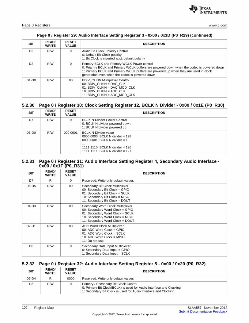
Page 0 Registers www.ti.com
Page 0 / Register 29: Audio Interface Setting Register 3 - 0x00 / 0x1D (P0_R29) (continued)
READ/ RESETBIT DESCRIPTIONWRITE VALUE
D3 R/W 0 Audio Bit Clock Polarity Control0: Default Bit Clock polarity1: Bit Clock is inverted w.r.t. default polarity
D2 R/W 0 Primary BCLK and Primary WCLK Power control0: Priamry BCLK and Primary WCLK buffers are powered down when the codec is powered down1: Primary BCLK and Primary WCLK buffers are powered up when they are used in clockgeneration even when the codec is powered down
D1-D0 R/W 00 BDIV_CLKIN Multiplexer Control00: BDIV_CLKIN = DAC_CLK01: BDIV_CLKIN = DAC_MOD_CLK10: BDIV_CLKIN = ADC_CLK11: BDIV_CLKIN = ADC_MOD_CLK
5.2.30 Page 0 / Register 30: Clock Setting Register 12, BCLK N Divider - 0x00 / 0x1E (P0_R30)READ/ RESETBIT DESCRIPTIONWRITE VALUE
D7 R/W 0 BCLK N Divider Power Control0: BCLK N divider powered down1: BCLK N divider powered up
D6-D0 R/W 000 0001 BCLK N Divider value0000 0000: BCLK N divider = 1280000 0001: BCLK N divider = 1…1111 1110: BCLK N divider = 1261111 1111: BCLK N divider = 127
5.2.31 Page 0 / Register 31: Audio Interface Setting Register 4, Secondary Audio Interface -0x00 / 0x1F (P0_R31)
READ/ RESETBIT DESCRIPTIONWRITE VALUE
D7 R 0 Reserved. Write only default values
D6-D5 R/W 00 Secondary Bit Clock Multiplexer00: Secondary Bit Clock = GPIO01: Secondary Bit Clock = SCLK10: Secondary Bit Clock = MISO11: Secondary Bit Clock = DOUT
D4-D3 R/W 00 Secondary Word Clock Multiplexer00: Secondary Word Clock = GPIO01: Secondary Word Clock = SCLK10: Secondary Word Clock = MISO11: Secondary Word Clock = DOUT
D2-D1 R/W 00 ADC Word Clock Multiplexer00: ADC Word Clock = GPIO01: ADC Word Clock = SCLK10: ADC Word Clock = MISO11: Do not use
D0 R/W 0 Secondary Data Input Multiplexer0: Secondary Data Input = GPIO1: Secondary Data Input = SCLK
5.2.32 Page 0 / Register 32: Audio Interface Setting Register 5 - 0x00 / 0x20 (P0_R32)READ/ RESETBIT DESCRIPTIONWRITE VALUE
D7-D4 R 0000 Reserved. Write only default values
D3 R/W 0 Primary / Secondary Bit Clock Control0: Primary Bit Clock(BCLK) is used for Audio Interface and Clocking1: Secondary Bit Clock is used for Audio Interface and Clocking
102 Register Map SLAA557–November 2012Submit Documentation Feedback
Copyright © 2012, Texas Instruments Incorporated

www.ti.com Page 0 Registers
Page 0 / Register 32: Audio Interface Setting Register 5 - 0x00 / 0x20 (P0_R32) (continued)
READ/ RESETBIT DESCRIPTIONWRITE VALUE
D2 R/W 0 Primary / Secondary Word Clock Control0: Primary Word Clock(WCLK) is used for Audio Interface1: Secondary Word Clock is used for Audio Interface
D1 R/W 0 ADC Word Clock Control0: ADC Word Clock is same as DAC Word Clock1: ADC Word Clock is Secondary ADC Word Clock
D0 R/W 0 Audio Data In Control0: DIN is used for Audio Data In1: Secondary Data In is used for Audio Data In
5.2.33 Page 0 / Register 33: Audio Interface Setting Register 6 - 0x00 / 0x21 (P0_R33)READ/ RESETBIT DESCRIPTIONWRITE VALUE
D7 R/W 0 BCLK Output Control0: BCLK Output = Generated Primary Bit Clock1: BCLK Output = Secondary Bit Clock Input
D6 R/W 0 Secondary Bit Clock Output Control0: Secondary Bit Clock = BCLK input1: Secondary Bit Clock = Generated Primary Bit Clock
D5-D4 R/W 00 WCLK Output Control00: WCLK Output = Generated DAC_FS01: WCLK Output = Generated ADC_FS10: WCLK Output = Secondary Word Clock Input11: Reserved. Do not use
D3-D2 R/W 00 Secondary Word Clock Output Control00: Secondary Word Clock output = WCLK input01: Secondary Word Clock output = Generated DAC_FS10: Secondary Word Clock output = Generated ADC_FS11: Reserved. Do not use
D1 R/W 0 Primary Data Out output control0: DOUT output = Data Output from Serial Interface1: DOUT output = Secondary Data Input (Loopback)
D0 R/W 0 Secondary Data Out output control0: Secondary Data Output = DIN input (Loopback)1: Secondary Data Output = Data output from Serial Interface
5.2.34 Page 0 / Register 34: Digital Interface Misc. Setting Register - 0x00 / 0x22 (P0_R34)READ/ RESETBIT DESCRIPTIONWRITE VALUE
D7 R 0 Reserved. Write only default value
D6 R 0 Reserved. Write only default value
D5 R/W 0 I2C General Call Address Configuration0: I2C General Call Address will be ignored1: I2C General Call Address accepted
D4-D0 R 0 0000 Reserved. Write only default values
5.2.35 Page 0 / Register 35: Reserved Register - 0x00 / 0x23 (P0_R35)READ/ RESETBIT DESCRIPTIONWRITE VALUE
D7-D0 R 0000 0000 Reserved. Write only default value
103SLAA557–November 2012 Register MapSubmit Documentation Feedback
Copyright © 2012, Texas Instruments Incorporated

Page 0 Registers www.ti.com
5.2.36 Page 0 / Register 36: ADC Flag Register - 0x00 / 0x24 (P0_R36)READ/ RESETBIT DESCRIPTIONWRITE VALUE
D7 R 0 Left ADC PGA Status Flag0: Gain Applied in Left ADC PGA is not equal to Programmed Gain in Control Register1: Gain Applied in Left ADC PGA is equal to Programmed Gain in Control Register
D6 R 0 Left ADC Power Status Flag0: Left ADC Powered Down1: Left ADC Powered Up
D5 R 0 Left AGC Gain Status. This sticky flag will self clear on reading0: Gain in Left AGC is not saturated1: Gain in Left ADC is equal to maximum allowed gain in Left AGC
D4 R 0 Reserved. Write only default values
D3 R 0 Right ADC PGA Status Flag0: Gain Applied in Right ADC PGA is not equal to Programmed Gain in Control Register1: Gain Applied in Right ADC PGA is equal to Programmed Gain in Control Register
D2 R 0 Right ADC Power Status Flag0: Right ADC Powered Down1: Right ADC Powered Up
D1 R 0 Right AGC Gain Status. This sticky flag will self clear on reading0: Gain in Right AGC is not saturated1: Gain in Right ADC is equal to maximum allowed gain in Right AGC
D0 R 0 Reserved. Write only default values
5.2.37 Page 0 / Register 37: DAC Flag Register 1 - 0x00 / 0x25 (P0_R37)READ/ RESETBIT DESCRIPTIONWRITE VALUE
D7 R 0 Left DAC Power Status Flag0: Left DAC Powered Down1: Left DAC Powered Up
D6 R 0 Left Line Output Driver(LOL) Power Status Flag0: LOL Powered Down1: LOL Powered Up
D5 R 0 Left Headphone Driver (HPL) Power Status Flag0: HPL Powered Down1: HPL Powered Up
D4 R 0 Reserved. Write only default values
D3 R 0 Right DAC Power Status Flag0: Right DAC Powered Down1: Right DAC Powered Up
D2 R 0 Right Line Output Driver(LOR) Power Status Flag0: LOR Powered Down1: LOR Powered Up
D1 R 0 Right Headphone Driver (HPR) Power Status Flag0: HPR Powered Down1: HPR Powered Up
D0 R 0 Reserved. Write only default values
5.2.38 Page 0 / Register 38: DAC Flag Register 2 - 0x00 / 0x26 (P0_R38)READ/ RESETBIT DESCRIPTIONWRITE VALUE
D7-D5 R 000 Reserved. Write only default values
D4 R 0 Left DAC PGA Status Flag0: Gain applied in Left DAC PGA is not equal to Gain programmed in Control Register1: Gain applied in Left DAC PGA is equal to Gain programmed in Control Register
D3-D1 R 000 Reserved. Write only default values
D0 R 0 Right DAC PGA Status Flag0: Gain applied in Right DAC PGA is not equal to Gain programmed in Control Register1: Gain applied in Right DAC PGA is equal to Gain programmed in Control Register
104 Register Map SLAA557–November 2012Submit Documentation Feedback
Copyright © 2012, Texas Instruments Incorporated

www.ti.com Page 0 Registers
5.2.39 Page 0 / Register 39-41: Reserved Register - 0x00 / 0x27-0x29 (P0_R39-41)READ/ RESETBIT DESCRIPTIONWRITE VALUE
D7-D0 R 0000 0000 Reserved. Write only default values
5.2.40 Page 0 / Register 42: Sticky Flag Register 1 - 0x00 / 0x2A (P0_R42)READ/ RESETBIT DESCRIPTIONWRITE VALUE
D7 R 0 Left DAC Overflow Status. This sticky flag will self clear on read0: No overflow in Left DAC1: Overflow has happened in Left DAC since last read of this register
D6 R 0 Right DAC Overflow Status. This sticky flag will self clear on read0: No overflow in Right DAC1: Overflow has happened in Right DAC since last read of this register
D5-D4 R 00 Reserved. Write only default values
D3 R 0 Left ADC Overflow Status. This sticky flag will self clear on read0: No overflow in Left ADC1: Overflow has happened in Left ADC since last read of this register
D2 R 0 Right ADC Overflow Status. This sticky flag will self clear on read0: No overflow in Right ADC1: Overflow has happened in Right ADC since last read of this register
D1-D0 R 00 Reserved. Write only default values
5.2.41 Page 0 / Register 43: Interrupt Flag Register 1 - 0x00 / 0x2B (P0_R43)READ/ RESETBIT DESCRIPTIONWRITE VALUE
D7 R 0 Left DAC Overflow Status.0: No overflow in Left DAC1: Overflow condition is present in Left ADC at the time of reading the register
D6 R 0 Right DAC Overflow Status.0: No overflow in Right DAC1: Overflow condition is present in Right DAC at the time of reading the register
D5-D4 R 00 Reserved. Write only default values
D3 R 0 Left ADC Overflow Status.0: No overflow in Left ADC1: Overflow condition is present in Left ADC at the time of reading the register
D2 R 0 Right ADC Overflow Status.0: No overflow in Right ADC1: Overflow condition is present in Right ADC at the time of reading the register
D1-D0 R 0 Reserved. Write only default values
5.2.42 Page 0 / Register 44: Sticky Flag Register 2 - 0x00 / 0x2C (P0_R44)READ/ RESETBIT DESCRIPTIONWRITE VALUE
D7 R 0 HPL Over Current Detect Flag0: Over Current not detected on HPL1: Over Current detected on HPL (will be cleared when the register is read)
D6 R 0 HPR Over Current Detect Flag0: Over Current not detected on HPR1: Over Current detected on HPR (will be cleared when the register is read)
D5 R 0 Headset Button Press0: Button Press not detected1: Button Press detected (will be cleared when the register is read)
D4 R 0 Headset Insertion/Removal Detect Flag0: Insertion/Removal event not detected1: Insertion/Removal event detected (will be cleared when the register is read)
D3 R 0 Left Channel DRC, Signal Threshold Flag0: Signal Power is below Signal Threshold1: Signal Power exceeded Signal Threshold (will be cleared when the register is read)
105SLAA557–November 2012 Register MapSubmit Documentation Feedback
Copyright © 2012, Texas Instruments Incorporated

Page 0 Registers www.ti.com
Page 0 / Register 44: Sticky Flag Register 2 - 0x00 / 0x2C (P0_R44) (continued)
READ/ RESETBIT DESCRIPTIONWRITE VALUE
D2 R 0 Right Channel DRC, Signal Threshold Flag0: Signal Power is below Signal Threshold1: Signal Power exceeded Signal Threshold (will be cleared when the register is read)
D1-D0 R 00 Reserved. Write only default values
5.2.43 Page 0 / Register 45: Sticky Flag Register 3 - 0x00 / 0x2D (P0_R45)READ/ RESETBIT DESCRIPTIONWRITE VALUE
D7 R 0 Reserved. Write only default values
D6 R 0 Left AGC Noise Threshold Flag0: Signal Power is greater than Noise Threshold1: Signal Power was lower than Noise Threshold (will be cleared when the register is read)
D5 R 0 Right AGC Noise Threshold Flag0: Signal Power is greater than Noise Threshold1: Signal Power was lower than Noise Threshold (will be cleared when the register is read)
D4-D3 R 00 Reserved. Write only default values
D2 R 0 Left ADC DC Measurement Data Available Flag0: Data not available1: Data available (will be cleared when the register is read)
D1 R 0 Right ADC DC Measurement Data Available Flag0: Data not available1: Data available (will be cleared when the register is read)
D0 R 0 Reserved. Write only default values
5.2.44 Page 0 / Register 46: Interrupt Flag Register 2 - 0x00 / 0x2E (P0_R46)READ/ RESETBIT DESCRIPTIONWRITE VALUE
D7 R 0 HPL Over Current Detect Flag0: Over Current not detected on HPL1: Over Current detected on HPL
D6 R 0 HPR Over Current Detect Flag0: Over Current not detected on HPR1: Over Current detected on HPR
D5 R 0 Headset Button Press0: Button Press not detected1: Button Press detected
D4 R 0 Headset Insertion/Removal Detect Flag0: Headset removal detected1: Headset insertion detected
D3 R 0 Left Channel DRC, Signal Threshold Flag0: Signal Power is below Signal Threshold1: Signal Power exceeded Signal Threshold
D2 R 0 Right Channel DRC, Signal Threshold Flag0: Signal Power is below Signal Threshold1: Signal Power exceeded Signal Threshold
D1-D0 R 00 Reserved. Write only default values
5.2.45 Page 0 / Register 47: Interrupt Flag Register 3 - 0x00 / 0x2F (P0_R47)READ/ RESETBIT DESCRIPTIONWRITE VALUE
D7 R 0 Reserved. Write only default values
D6 R 0 Left AGC Noise Threshold Flag0: Signal Power is greater than Noise Threshold1: Signal Power was lower than Noise Threshold
106 Register Map SLAA557–November 2012Submit Documentation Feedback
Copyright © 2012, Texas Instruments Incorporated
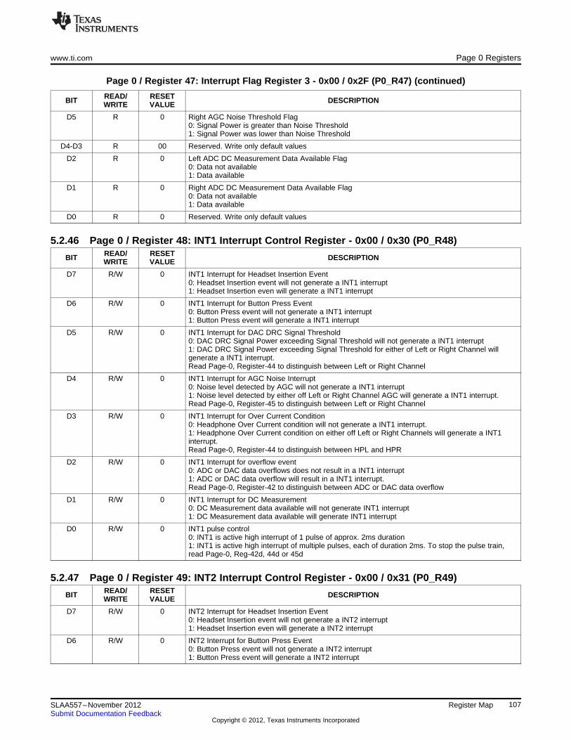
www.ti.com Page 0 Registers
Page 0 / Register 47: Interrupt Flag Register 3 - 0x00 / 0x2F (P0_R47) (continued)
READ/ RESETBIT DESCRIPTIONWRITE VALUE
D5 R 0 Right AGC Noise Threshold Flag0: Signal Power is greater than Noise Threshold1: Signal Power was lower than Noise Threshold
D4-D3 R 00 Reserved. Write only default values
D2 R 0 Left ADC DC Measurement Data Available Flag0: Data not available1: Data available
D1 R 0 Right ADC DC Measurement Data Available Flag0: Data not available1: Data available
D0 R 0 Reserved. Write only default values
5.2.46 Page 0 / Register 48: INT1 Interrupt Control Register - 0x00 / 0x30 (P0_R48)READ/ RESETBIT DESCRIPTIONWRITE VALUE
D7 R/W 0 INT1 Interrupt for Headset Insertion Event0: Headset Insertion event will not generate a INT1 interrupt1: Headset Insertion even will generate a INT1 interrupt
D6 R/W 0 INT1 Interrupt for Button Press Event0: Button Press event will not generate a INT1 interrupt1: Button Press event will generate a INT1 interrupt
D5 R/W 0 INT1 Interrupt for DAC DRC Signal Threshold0: DAC DRC Signal Power exceeding Signal Threshold will not generate a INT1 interrupt1: DAC DRC Signal Power exceeding Signal Threshold for either of Left or Right Channel willgenerate a INT1 interrupt.Read Page-0, Register-44 to distinguish between Left or Right Channel
D4 R/W 0 INT1 Interrupt for AGC Noise Interrupt0: Noise level detected by AGC will not generate a INT1 interrupt1: Noise level detected by either off Left or Right Channel AGC will generate a INT1 interrupt.Read Page-0, Register-45 to distinguish between Left or Right Channel
D3 R/W 0 INT1 Interrupt for Over Current Condition0: Headphone Over Current condition will not generate a INT1 interrupt.1: Headphone Over Current condition on either off Left or Right Channels will generate a INT1interrupt.Read Page-0, Register-44 to distinguish between HPL and HPR
D2 R/W 0 INT1 Interrupt for overflow event0: ADC or DAC data overflows does not result in a INT1 interrupt1: ADC or DAC data overflow will result in a INT1 interrupt.Read Page-0, Register-42 to distinguish between ADC or DAC data overflow
D1 R/W 0 INT1 Interrupt for DC Measurement0: DC Measurement data available will not generate INT1 interrupt1: DC Measurement data available will generate INT1 interrupt
D0 R/W 0 INT1 pulse control0: INT1 is active high interrupt of 1 pulse of approx. 2ms duration1: INT1 is active high interrupt of multiple pulses, each of duration 2ms. To stop the pulse train,read Page-0, Reg-42d, 44d or 45d
5.2.47 Page 0 / Register 49: INT2 Interrupt Control Register - 0x00 / 0x31 (P0_R49)READ/ RESETBIT DESCRIPTIONWRITE VALUE
D7 R/W 0 INT2 Interrupt for Headset Insertion Event0: Headset Insertion event will not generate a INT2 interrupt1: Headset Insertion even will generate a INT2 interrupt
D6 R/W 0 INT2 Interrupt for Button Press Event0: Button Press event will not generate a INT2 interrupt1: Button Press event will generate a INT2 interrupt
107SLAA557–November 2012 Register MapSubmit Documentation Feedback
Copyright © 2012, Texas Instruments Incorporated

Page 0 Registers www.ti.com
Page 0 / Register 49: INT2 Interrupt Control Register - 0x00 / 0x31 (P0_R49) (continued)
READ/ RESETBIT DESCRIPTIONWRITE VALUE
D5 R/W 0 INT2 Interrupt for DAC DRC Signal Threshold0: DAC DRC Signal Power exceeding Signal Threshold will not generate a INT2 interrupt1: DAC DRC Signal Power exceeding Signal Threshold for either of Left or Right Channel willgenerate a INT2 interrupt.Read Page-0, Register-44 to distinguish between Left or Right Channel
D4 R/W 0 INT2 Interrupt for AGC Noise Interrupt0: Noise level detected by AGC will not generate a INT2 interrupt1: Noise level detected by either off Left or Right Channel AGC will generate a INT2 interrupt.Read Page-0, Register-45 to distinguish between Left or Right Channel
D3 R/W 0 INT2 Interrupt for Over Current Condition0: Headphone Over Current condition will not generate a INT2 interrupt.1: Headphone Over Current condition on either off Left or Right Channels will generate a INT2interrupt.Read Page-0, Register-44 to distinguish between HPL and HPR
D2 R/W 0 INT2 Interrupt for overflow event0: ADC or DAC data overflow will not result in an INT2 interrupt1: ADC or DAC data overflow will result in an INT2 interrupt.Read Page-0, Register-42 to distinguish between ADC or DAC data overflow
D1 R/W 0 INT2 Interrupt for DC Measurement0: DC Measurement data available will not generate INT2 interrupt1: DC Measurement data available will generate INT2 interrupt
D0 R/W 0 INT2 pulse control0: INT2 is active high interrupt of 1 pulse of approx. 2ms duration1: INT2 is active high interrupt of multiple pulses, each of duration 2ms. To stop the pulse train,read Page-0, Reg-42d, 44d and 45d
5.2.48 Page 0 / Register 50-51: Reserved Register - 0x00 / 0x32-0x33 (P0_R50-51)READ/ RESETBIT DESCRIPTIONWRITE VALUE
D7-D0 R 0000 0000 Reserved. Write only default values
5.2.49 Page 0 / Register 52: GPIO/MFP5 Control Register - 0x00 / 0x34 (P0_R52)READ/ RESETBIT DESCRIPTIONWRITE VALUE
D7-D6 R 00 Reserved. Write only default values
D5-D2 R/W 0000 GPIO Control0000: GPIO input/output disabled.0001: GPIO input is used for secondary audio interface, digital microphone input or clock input.Configure other registers to choose the functionality of GPIO input0010: GPIO is general purpose input0011: GPIO is general purpose output0100: GPIO output is CLKOUT0101: GPIO output is INT10110: GPIO output is INT20111: GPIO output is ADC_WCLK for Audio Interface1000: GPIO output is secondary bit-clock for Audio Interface1001: GPIO output is secondary word-clock for Audio Interface1010: GPIO output is clock for digital microphone1011-1111: Reserved. Do not use.
D1 R X GPIO Input Pin state, used along with GPIO as general purpose input
D0 R/W 0 GPIO as general purpose output control0: GPIO pin is driven to '0' in general purpose output mode1: GPIO pin is driven to '1' in general purpose output mode
5.2.50 Page 0 / Register 53: DOUT/MFP2 Function Control Register - 0x00 / 0x35 (P0_R53)READ/ RESETBIT DESCRIPTIONWRITE VALUE
D7-D5 R 000 Reserved. Write only default values
108 Register Map SLAA557–November 2012Submit Documentation Feedback
Copyright © 2012, Texas Instruments Incorporated

www.ti.com Page 0 Registers
Page 0 / Register 53: DOUT/MFP2 Function Control Register - 0x00 / 0x35 (P0_R53) (continued)
READ/ RESETBIT DESCRIPTIONWRITE VALUE
D4 R/W 1 DOUT Bus Keeper Control0: DOUT Bus Keeper Enabled1: DOUT Bus Keeper Disabled
D3-D1 R/W 001 DOUT MUX Control000: DOUT disabled001: DOUT is Primary DOUT010: DOUT is General Purpose Output011: DOUT is CLKOUT100: DOUT is INT1101: DOUT is INT2110: DOUT is Secondary BCLK111: DOUT is Secondary WCLK
D0 R/W 0 DOUT as General Purpose Output0: DOUT General Purpose Output is '0'1: DOUT General Purpose Output is '1'
5.2.51 Page 0 / Register 54: DIN/MFP1 Function Control Register - 0x00 / 0x36 (P0_R54)READ/ RESETBIT DESCRIPTIONWRITE VALUE
D7-D3 R 0 0000 Reserved. Write only reserved values
D2-D1 R/W 01 DIN function control00: DIN pin is disabled01: DIN is enabled for Primary Data Input or Digital Microphone Input or General Purpose Clockinput10: DIN is used as General Purpose Input11: Reserved. Do not use
D0 R X Value of DIN input pin. To be used when for General Purpose Input
5.2.52 Page 0 / Register 55: MISO/MFP4 Function Control Register - 0x00 / 0x37 (P0_R55)READ/ RESETBIT DESCRIPTIONWRITE VALUE
D7-D5 R 000 Reserved. Write only default values
D4-D1 R/W 0001 MISO function control0000: MISO buffer disabled0001: MISO is used for data output in SPI interface, is disabled for I2C interface0010: MISO is General Purpose Output0011: MISO is CLKOUT output0100: MISO is INT1 output0101: MISO is INT2 output0110: MISO is ADC Word Clock output0111: MISO is clock output for Digital Microphone1000: MISO is Secondary Data Output for Audio Interface1001: MISO is Secondary Bit Clock for Audio Interface1010: MISO is Secondary Word Clock for Audio Interface1011-1111: Reserved. Do not use
D0 R/W 0 Value to be driven on MISO pin when used as General Purpose Output
5.2.53 Page 0 / Register 56: SCLK/MFP3 Function Control Register - 0x00 / 0x38 (P0_R56)READ/ RESETBIT DESCRIPTIONWRITE VALUE
D7-D3 R 0 0000 Reserved. Write only default values
D2-D1 R/W 01 SCLK function control00: SCLK pin is disabled01: SCLK pin is enabled for SPI clock in SPI Interface mode or when in I2C Interface enabled forSecondary Data Input or Secondary Bit Clock Input or Secondary Word Clock or Secondary ADCWord Clock or Digital Microphone Input10: SCLK is enabled as General Purpose Input11: Reserved. Do not use
D0 R X Value of SCLK input pin when used as General Purpose Input
109SLAA557–November 2012 Register MapSubmit Documentation Feedback
Copyright © 2012, Texas Instruments Incorporated

Page 0 Registers www.ti.com
5.2.54 Page 0 / Register 57-59: Reserved Registers - 0x00 / 0x39-0x3B (P0_R57-59)READ/ RESETBIT DESCRIPTIONWRITE VALUE
D7-D0 R 0000 0000 Reserved. Write only default values
5.2.55 Page 0 / Register 60: DAC Signal Processing Block Control Register - 0x00 / 0x3C(P0_R60)
READ/ RESETBIT DESCRIPTIONWRITE VALUE
D7-D5 R 000 Reserved. Write only default values
D4-D0 R/W 0 0001 Selects the DAC (playback) signal processing block0 0000: Reserved. Do not use0 0001: DAC Signal Processing Block PRB_P10 0010: DAC Signal Processing Block PRB_P20 0011: DAC Signal Processing Block PRB_P30 0100: DAC Signal Processing Block PRB_P4…1 1000: DAC Signal Processing Block PRB_P241 1001: DAC Signal Processing Block PRB_P251 1010-1 1111: Reserved. Do not useNote; Please check the overview section for description of the Signal Processing Blocks
5.2.56 Page 0 / Register 61: ADC Signal Processing Block Control Register - 0x00 / 0x3D(P0_R61)
READ/ RESETBIT DESCRIPTIONWRITE VALUE
D7-D5 R 000 Reserved. Write only default values
D4-D0 R/W 0 0001 Selects the ADC (recording) signal processing block0 0000: Reserved. Do not use0 0001: ADC Singal Processing Block PRB_R10 0010: ADC Signal Processing Block PRB_R20 0011: ADC Signal Processing Block PRB_R30 0100: ADC Signal Processing Block PRB_R4…1 0001: ADC Signal Processing Block PRB_R171 0010: ADC Signal Processing Block PRB_R181 0010-1 1111: Reserved. Do not useNote: Please check the overview section for description of the Signal Processing Blocks
5.2.57 Page 0 / Register 62: Reserved Register - 0x00 / 0x3E (P0_R62)READ/ RESETBIT DESCRIPTIONWRITE VALUE
D7-D0 R 0000 0000 Reserved. Write only default values
5.2.58 Page 0 / Register 63: DAC Channel Setup Register 1 - 0x00 / 0x3F (P0_R63)READ/ RESETBIT DESCRIPTIONWRITE VALUE
D7 R/W 0 Left DAC Channel Power Control0: Left DAC Channel Powered Down1: Left DAC Channel Powered Up
D6 R/W 0 Right DAC Channel Power Control0: Right DAC Channel Powered Down1: Right DAC Channel Powered Up
D5-D4 R/W 01 Left DAC Data path Control00: Left DAC data is disabled01: Left DAC data Left Channel Audio Interface Data10: Left DAC data is Right Channel Audio Interface Data11: Left DAC data is Mono Mix of Left and Right Channel Audio Interface Data
110 Register Map SLAA557–November 2012Submit Documentation Feedback
Copyright © 2012, Texas Instruments Incorporated

www.ti.com Page 0 Registers
Page 0 / Register 63: DAC Channel Setup Register 1 - 0x00 / 0x3F (P0_R63) (continued)
READ/ RESETBIT DESCRIPTIONWRITE VALUE
D3-D2 R/W 01 Right DAC Data path Control00: Right DAC data is disabled01: Right DAC data Right Channel Audio Interface Data10: Right DAC data is Left Channel Audio Interface Data11: Right DAC data is Mono Mix of Left and Right Channel Audio Interface Data
D1-D0 R/W 00 DAC Channel Volume Control's Soft-Step control00: Soft-Stepping is 1 step per 1 DAC Word Clock01: Soft-Stepping is 1 step per 2 DAC Word Clocks10: Soft-Stepping is disabled11: Reserved. Do not use
5.2.59 Page 0 / Register 64: DAC Channel Setup Register 2 - 0x00 / 0x40 (P0_R64)READ/ RESETBIT DESCRIPTIONWRITE VALUE
D7 R/W 0 Right Modulator Output Control0: When Right DAC Channel is powered down, the data is zero.1: When Right DAC Channel is powered down, the data is inverted version of Left DAC ModulatorOutput. Can be used when differential mono output is used
D6-D4 R/W 000 DAC Auto Mute Control000: Auto Mute disabled001: DAC is auto muted if input data is DC for more than 100 consecutive inputs010: DAC is auto muted if input data is DC for more than 200 consecutive inputs011: DAC is auto muted if input data is DC for more than 400 consecutive inputs100: DAC is auto muted if input data is DC for more than 800 consecutive inputs101: DAC is auto muted if input data is DC for more than 1600 consecutive inputs110: DAC is auto muted if input data is DC for more than 3200 consecutive inputs111: DAC is auto muted if input data is DC for more than 6400 consecutive inputs
D3 R/W 1 Left DAC Channel Mute Control0: Left DAC Channel not muted1: Left DAC Channel muted
D2 R/W 1 Right DAC Channel Mute Control0: Right DAC Channel not muted1: Right DAC Channel muted
D1-D0 R/W 00 DAC Master Volume Control00: Left and Right Channel have independent volume control01: Left Channel Volume is controlled by Right Channel Volume Control setting10: Right Channel Volume is controlled by Left Channel Volume Control setting11: Reserved. Do not use
5.2.60 Page 0 / Register 65: Left DAC Channel Digital Volume Control Register - 0x00 / 0x41(P0_R65)
READ/ RESETBIT DESCRIPTIONWRITE VALUE
D7-D0 R/W 0000 0000 Left DAC Channel Digital Volume Control Setting0111 1111-0011 0001: Reserved. Do not use0011 0000: Digital Volume Control = +24dB0010 1111: Digital Volume Control = +23.5dB…0000 0001: Digital Volume Control = +0.5dB0000 0000: Digital Volume Control = 0.0dB1111 1111: Digital Volume Control = -0.5dB...1000 0010: Digital Volume Control = -63dB1000 0001: Digital Volume Control = -63.5dB1000 0000: Reserved. Do not use
5.2.61 Page 0 / Register 66: Right DAC Channel Digital Volume Control Register - 0x00 / 0x42
111SLAA557–November 2012 Register MapSubmit Documentation Feedback
Copyright © 2012, Texas Instruments Incorporated

Page 0 Registers www.ti.com
(P0_R66)READ/ RESETBIT DESCRIPTIONWRITE VALUE
D7-D0 R/W 0000 0000 Right DAC Channel Digital Volume Control Setting0111 1111-0011 0001: Reserved. Do not use0011 0000: Digital Volume Control = +24dB0010 1111: Digital Volume Control = +23.5dB…0000 0001: Digital Volume Control = +0.5dB0000 0000: Digital Volume Control = 0.0dB1111 1111: Digital Volume Control = -0.5dB...1000 0010: Digital Volume Control = -63dB1000 0001: Digital Volume Control = -63.5dB1000 0000: Reserved. Do not use
5.2.62 Page 0 / Register 67: Headset Detection Configuration Register - 0x00 / 0x43 (P0_R67)READ/ RESETBIT DESCRIPTIONWRITE VALUE
D7 R/W 0 0: Headset Detection Disabled1: Headset Detection Enabled
D6-D5 R 00 Headset Type Flag00: Headset not detected01: Stereo Headset detected10: Reserved11: Stereo + Cellular Headset detected
D4-D2 R/W 000 Headset Detection Debounce Programmability000: Debounce Time = 16ms001: Debounce Time = 32ms010: Debounce Time = 64ms011: Debounce Time = 128ms100: Debounce Time = 256ms101: Debounce Time = 512ms110-111: Reserved. Do not useNote: All times are typical values
D1-D0 R/W 00 Headset Button Press Debounce Programmability00: Debounce disabled01: Debounce Time = 8ms10: Debounce Time = 16ms11: Debounce Time = 32msNote: All times are typical values
5.2.63 Page 0 / Register 68: DRC Control Register 1 - 0x00 / 0x44 (P0_R68)READ/ RESETBIT DESCRIPTIONWRITE VALUE
D7 R 0 Reserved. Write only default value
D6 R/W 1 DRC Enable Control0: Left Channel DRC disabled1: Left Channel DRC enabledNote: DRC only active if a PRB_Px has been selected that supports DRC
D5 R/W 1 DRC Enable Control0: Right Channel DRC disabled1: Right Channel DRC enabledNote: DRC only active if a PRB_Px has been selected that supports DRC
D4-D2 R/W 011 DRC Threshold control000: DRC Threshold = -3dBFS001: DRC Threshold = -6dBFS010: DRC Threshold = -9dBFS011: DRC Threshold = -12dBFS100: DRC Threshold = -15dBFS101: DRC Threshold = -18dBFS110: DRC Threshold = -21dBFS111: DRC Threshold = -24dBFS
112 Register Map SLAA557–November 2012Submit Documentation Feedback
Copyright © 2012, Texas Instruments Incorporated

www.ti.com Page 0 Registers
Page 0 / Register 68: DRC Control Register 1 - 0x00 / 0x44 (P0_R68) (continued)
READ/ RESETBIT DESCRIPTIONWRITE VALUE
D1-D0 R/W 11 DRC Hysteresis Control00: DRC Hysteresis = 0dB01: DRC Hysteresis = 1dB10: DRC Hysteresis = 2dB11: DRC Hysteresis = 3dB
5.2.64 Page 0 / Register 69: DRC Control Register 2 - 0x00 / 0x45 (P0_R69)READ/ RESETBIT DESCRIPTIONWRITE VALUE
D7 R 0 Reserved. Write only default value.
D6-D3 R/W 0111 DRC Hold Programmability0000: DRC Hold Disabled0001: DRC Hold Time = 32 DAC Word Clocks0010: DRC Hold Time = 64 DAC Word Clocks0011: DRC Hold Time = 128 DAC Word Clocks0100: DRC Hold Time = 256 DAC Word Clocks0101: DRC Hold Time = 512 DAC Word Clocks...1110: DRC Hold Time = 4*32768 DAC Word Clocks1111: DRC Hold Time = 5*32768 DAC Word Clocks
D2-D0 R/W 000 Reserved. Write only default values
5.2.65 Page 0 / Register 70: DRC Control Register 3 - 0x00 / 0x46 (P0_R70)READ/ RESETBIT DESCRIPTIONWRITE VALUE
D7-D4 R/W 0000 DRC Attack Rate control0000: DRC Attack Rate = 4.0dB per DAC Word Clock0001: DRC Attack Rate = 2.0dB per DAC Word Clock0010: DRC Attack Rae = 1.0dB per DAC Word Clock…1110: DRC Attack Rate = 2.4414e-4dB per DAC Word Clock1111: DRC Attack Rate = 1.2207e-4dB per DAC Word Clock
D3-D0 R/W 0000 DRC Decay Rate control0000: DRC Decay Rate = 1.5625e-2dB per DAC Word Clock0001: DRC Decay Rate = 7.8125e-3dB per DAC Word Clock0010: DRC Decay Rae = 3.9062e-3dB per DAC Word Clock…1110: DRC Decay Rate = 9.5367e-7dB per DAC Word Clock1111: DRC Decay Rate = 4.7683e-7dB per DAC Word Clock
5.2.66 Page 0 / Register 71: Beep Generator Register 1 - 0x00 / 0x47 (P0_R71)READ/ RESETBIT DESCRIPTIONWRITE VALUE
D7 R/W 0 0: Beep Generator Disabled1: Beep Generator Enabled. This bit will self clear after the beep has been generated.
D6 R 0 Reserved. Write only default value
D5-D0 R/W 00 0000 Left Channel Beep Volume Control00 0000: Left Channel Beep Volume = 0dB00 0001: Left Channel Beep Volume = -1dB…11 1110: Left Channel Beep Volume = -62dB11 1111: Left Channel Beep Volume = -63dB
113SLAA557–November 2012 Register MapSubmit Documentation Feedback
Copyright © 2012, Texas Instruments Incorporated
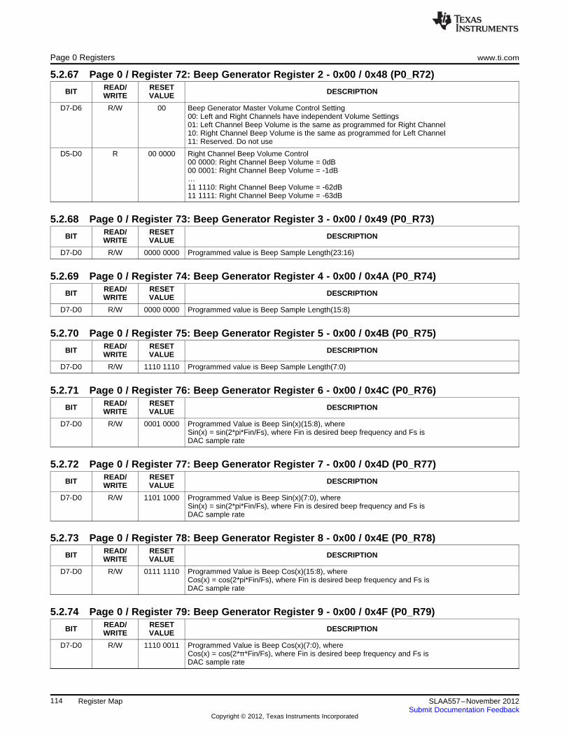
Page 0 Registers www.ti.com
5.2.67 Page 0 / Register 72: Beep Generator Register 2 - 0x00 / 0x48 (P0_R72)READ/ RESETBIT DESCRIPTIONWRITE VALUE
D7-D6 R/W 00 Beep Generator Master Volume Control Setting00: Left and Right Channels have independent Volume Settings01: Left Channel Beep Volume is the same as programmed for Right Channel10: Right Channel Beep Volume is the same as programmed for Left Channel11: Reserved. Do not use
D5-D0 R 00 0000 Right Channel Beep Volume Control00 0000: Right Channel Beep Volume = 0dB00 0001: Right Channel Beep Volume = -1dB…11 1110: Right Channel Beep Volume = -62dB11 1111: Right Channel Beep Volume = -63dB
5.2.68 Page 0 / Register 73: Beep Generator Register 3 - 0x00 / 0x49 (P0_R73)READ/ RESETBIT DESCRIPTIONWRITE VALUE
D7-D0 R/W 0000 0000 Programmed value is Beep Sample Length(23:16)
5.2.69 Page 0 / Register 74: Beep Generator Register 4 - 0x00 / 0x4A (P0_R74)READ/ RESETBIT DESCRIPTIONWRITE VALUE
D7-D0 R/W 0000 0000 Programmed value is Beep Sample Length(15:8)
5.2.70 Page 0 / Register 75: Beep Generator Register 5 - 0x00 / 0x4B (P0_R75)READ/ RESETBIT DESCRIPTIONWRITE VALUE
D7-D0 R/W 1110 1110 Programmed value is Beep Sample Length(7:0)
5.2.71 Page 0 / Register 76: Beep Generator Register 6 - 0x00 / 0x4C (P0_R76)READ/ RESETBIT DESCRIPTIONWRITE VALUE
D7-D0 R/W 0001 0000 Programmed Value is Beep Sin(x)(15:8), whereSin(x) = sin(2*pi*Fin/Fs), where Fin is desired beep frequency and Fs isDAC sample rate
5.2.72 Page 0 / Register 77: Beep Generator Register 7 - 0x00 / 0x4D (P0_R77)READ/ RESETBIT DESCRIPTIONWRITE VALUE
D7-D0 R/W 1101 1000 Programmed Value is Beep Sin(x)(7:0), whereSin(x) = sin(2*pi*Fin/Fs), where Fin is desired beep frequency and Fs isDAC sample rate
5.2.73 Page 0 / Register 78: Beep Generator Register 8 - 0x00 / 0x4E (P0_R78)READ/ RESETBIT DESCRIPTIONWRITE VALUE
D7-D0 R/W 0111 1110 Programmed Value is Beep Cos(x)(15:8), whereCos(x) = cos(2*pi*Fin/Fs), where Fin is desired beep frequency and Fs isDAC sample rate
5.2.74 Page 0 / Register 79: Beep Generator Register 9 - 0x00 / 0x4F (P0_R79)READ/ RESETBIT DESCRIPTIONWRITE VALUE
D7-D0 R/W 1110 0011 Programmed Value is Beep Cos(x)(7:0), whereCos(x) = cos(2*π*Fin/Fs), where Fin is desired beep frequency and Fs isDAC sample rate
114 Register Map SLAA557–November 2012Submit Documentation Feedback
Copyright © 2012, Texas Instruments Incorporated

www.ti.com Page 0 Registers
5.2.75 Page 0 / Register 80: Reserved Register - 0x00 / 0x50 (P0_R80)READ/ RESETBIT DESCRIPTIONWRITE VALUE
D7-D0 R 0000 0000 Reserved. Write only default values
5.2.76 Page 0 / Register 81: ADC Channel Setup Register - 0x00 / 0x51 (P0_R81)READ/ RESETBIT DESCRIPTIONWRITE VALUE
D7 R/W 0 Left Channel ADC Power Control0: Left Channel ADC is powered down1: Left Channel ADC is powered up
D6 R/W 0 Right Channel ADC Power Control0: Right Channel ADC is powered down1: Right Channel ADC is powered up
D5-D4 R/W 00 Digital Microphone Input Configuration00: GPIO serves as Digital Microphone Input01: SCLK serves as Digital Microphone Input10: DIN serves as Digital Microphone Input11: Reserved. Do not use
D3 R/W 0 Left Channel Digital Microphone Power Control0: Left Channel ADC not configured for Digital Microphone1: Left Channel ADC configured for Digital Microphone
D2 R/W 0 Right Channel Digital Microphone Power Control0: Right Channel ADC not configured for Digital Microphone1: Right Channel ADC configured for Digital Microphone
D1-D0 R/W 00 ADC Volume Control Soft-Stepping Control00: ADC Volume Control changes by 1 gain step per ADC Word Clock01: ADC Volume Control changes by 1 gain step per two ADC Word Clocks10: ADC Volume Control Soft-Stepping disabled11: Reserved. Do not use
5.2.77 Page 0 / Register 82: ADC Fine Gain Adjust Register - 0x00 / 0x52 (P0_R82)READ/ RESETBIT DESCRIPTIONWRITE VALUE
D7 R/W 1 Left ADC Channel Mute Control0: Left ADC Channel Un-muted1: Left ADC Channel Muted
D6-D4 R/W 000 Left ADC Channel Fine Gain Adjust000: Left ADC Channel Fine Gain = 0dB111: Left ADC Channel Fine Gain = -0.1dB110: Left ADC Channel Fine Gain = -0.2dB101: Left ADC Channel Fine Gain = -0.3dB100: Left ADC Channel Fine Gain = -0.4dB001-011: Reserved. Do not use
D3 R/W 1 Right ADC Channel Mute Control0: Right ADC Channel Un-muted1: Right ADC Channel Muted
D2-D0 R/W 000 Right ADC Channel Fine Gain Adjust000: Right ADC Channel Fine Gain = 0dB111: Right ADC Channel Fine Gain = -0.1dB110: Right ADC Channel Fine Gain = -0.2dB101: Right ADC Channel Fine Gain = -0.3dB100: Right ADC Channel Fine Gain = -0.4dB001-011: Reserved. Do not use
5.2.78 Page 0 / Register 83: Left ADC Channel Volume Control Register - 0x00 / 0x53 (P0_R83)READ/ RESETBIT DESCRIPTIONWRITE VALUE
D7 R 0 Reserved. Write only default values
115SLAA557–November 2012 Register MapSubmit Documentation Feedback
Copyright © 2012, Texas Instruments Incorporated

Page 0 Registers www.ti.com
Page 0 / Register 83: Left ADC Channel Volume Control Register - 0x00 / 0x53 (P0_R83) (continued)
READ/ RESETBIT DESCRIPTIONWRITE VALUE
D6-D0 R/W 000 0000 Left ADC Channel Volume Control100 0000-110 0111: Reserved. Do not use110 1000: Left ADC Channel Volume = -12dB110 1001: Left ADC Channel Volume = -11.5dB110 1010: Left ADC Channel Volume = -11.0dB…111 1111: Left ADC Channel Volume = -0.5dB000 0000: Left ADC Channel Volume = 0.0dB000 0001: Left ADC Channel Volume = 0.5dB...010 0110: Left ADC Channel Volume = 19.0dB010 0111: Left ADC Channel Volume = 19.5dB010 1000: Left ADC Channel Volume = 20.0dB010 1001-111 1111: Reserved. Do not use
5.2.79 Page 0 / Register 84: Right ADC Channel Volume Control Register - 0x00 / 0x54(P0_R84)
READ/ RESETBIT DESCRIPTIONWRITE VALUE
D7 R 0 Reserved. Write only default values
D6-D0 R/W 000 0000 Right ADC Channel Volume Control100 0000-110 0111: Reserved. Do not use110 1000: Right ADC Channel Volume = -12dB110 1001: Right ADC Channel Volume = -11.5dB110 1010: Right ADC Channel Volume = -11.0dB…111 1111: Right ADC Channel Volume = -0.5dB000 0000: Right ADC Channel Volume = 0.0dB000 0001: Right ADC Channel Volume = 0.5dB...010 0110: Right ADC Channel Volume = 19.0dB010 0111: Right ADC Channel Volume = 19.5dB010 1000: Right ADC Channel Volume = 20.0dB010 1001-111 1111: Reserved. Do not use
5.2.80 Page 0 / Register 85: ADC Phase Adjust Register - 0x00 / 0x55 (P0_R85)READ/ RESETBIT DESCRIPTIONWRITE VALUE
D7-D0 R/W 0000 0000 ADC Phase Compensation Control1000 0000-1111 1111: Left ADC Channel Data is delayed with respect to Right ADC ChannelData. For details of delayed amount please refer to the description of Phase Compensation in theOverview section.0000 0000: Left and Right ADC Channel data are not delayed with respect to each other0000 0001-0111 1111: Right ADC Channel Data is delayed with respect to Left ADC ChannelData. For details of delayed amount please refer to the description of Phase Compensation in theOverview section.
5.2.81 Page 0 / Register 86: Left Channel AGC Control Register 1 - 0x00 / 0x56 (P0_R86)READ/ RESETBIT DESCRIPTIONWRITE VALUE
D7 R/W 0 0: Left Channel AGC Disabled1: Left Channel AGC Enabled
D6-D4 R/W 000 Left Channel AGC Target Level Setting000: Left Channel AGC Target Level = -5.5dBFS001: Left Channel AGC Target Level = -8.0dBFS010: Left Channel AGC Target Level = -10.0dBFS011: Left Channel AGC Target Level = -12.0dBFS100: Left Channel AGC Target Level = -14.0dBFS101: Left Channel AGC Target Level = -17.0dBFS110: Left Channel AGC Target Level = -20.0dBFS111: Left Channel AGC Target Level = -24.0dBFS
116 Register Map SLAA557–November 2012Submit Documentation Feedback
Copyright © 2012, Texas Instruments Incorporated

www.ti.com Page 0 Registers
Page 0 / Register 86: Left Channel AGC Control Register 1 - 0x00 / 0x56 (P0_R86) (continued)
READ/ RESETBIT DESCRIPTIONWRITE VALUE
D3-D2 R 00 Reserved. Write only default values
D1-D0 R/W 00 Left Channel AGC Gain Hysteresis Control00: Left Channel AGC Gain Hysteresis is disabled01: Left Channel AGC Gain Hysteresis is ±0.5dB10: Left Channel AGC Gain Hysteresis is ±1.0dB11: Left Channel AGC Gain Hysteresis is ±1.5dB
5.2.82 Page 0 / Register 87: Left Channel AGC Control Register 2 - 0x00 / 0x57 (P0_R87)READ/ RESETBIT DESCRIPTIONWRITE VALUE
D7-D6 R/W 00 Left Channel AGC Hysteresis Setting00: Left Channel AGC Hysteresis is 1.0dB01: Left Channel AGC Hysteresis is 2.0dB10: Left Channel AGC Hysteresis is 4.0dB11: Left Channel AGC Hysteresis is disabled
D5-D1 R/W 0 0000 Left Channel AGC Noise Threshold0 0000: Left Channel AGC Noise Gate disabled0 0001: Left Channel AGC Noise Threshold is -30dB0 0010: Left Channel AGC Noise Threshold is -32dB0 0011: Left Channel AGC Noise Threshold is -34dB…1 1101: Left Channel AGC Noise Threshold is -86dB1 1110: Left Channel AGC Noise Threshold is -88dB1 1111: Left Channel AGC Noise Threshold is -90dB
D0 R 0 Reserved. Write only default value
5.2.83 Page 0 / Register 88: Left Channel AGC Control Register 3 - 0x00 / 0x58 (P0_R88)READ/ RESETBIT DESCRIPTIONWRITE VALUE
D7 R 0 Reserved. Write only default value
D6-D0 R/W 111 1111 Left Channel AGC Maximum Gain Setting000 0000: Left Channel AGC Maximum Gain = 0.0dB000 0001: Left Channel AGC Maximum Gain = 0.5dB000 0010: Left Channel AGC Maximum Gain = 1.0dB…111 0011: Left Channel AGC Maximum Gain = 57.5dB111 0100: Left Channel AGC Maximum Gain = 58.0dB111 0101-111 1111: not recommended for usage, Left Channel AGC Maximum Gain = 58.0dB
5.2.84 Page 0 / Register 89: Left Channel AGC Control Register 4 - 0x00 / 0x59 (P0_R89)READ/ RESETBIT DESCRIPTIONWRITE VALUE
D7-D3 R/W 0 0000 Left Channel AGC Attack Time Setting0 0000: Left Channel AGC Attack Time = 1*32 ADC Word Clocks0 0001: Left Channel AGC Attack Time = 3*32 ADC Word Clocks0 0010: Left Channel AGC Attack Time = 5*32 ADC Word Clocks…1 1101: Left Channel AGC Attack Time = 59*32 ADC Word Clocks1 1110: Left Channel AGC Attack Time = 61*32 ADC Word Clocks1 1111: Left Channel AGC Attack Time = 63*32 ADC Word Clocks
D2-D0 R/W 000 Left Channel AGC Attack Time Scale Factor Setting000: Scale Factor = 1001: Scale Factor = 2010: Scale Factor = 4…101: Scale Factor = 32110: Scale Factor = 64111: Scale Factor = 128
117SLAA557–November 2012 Register MapSubmit Documentation Feedback
Copyright © 2012, Texas Instruments Incorporated
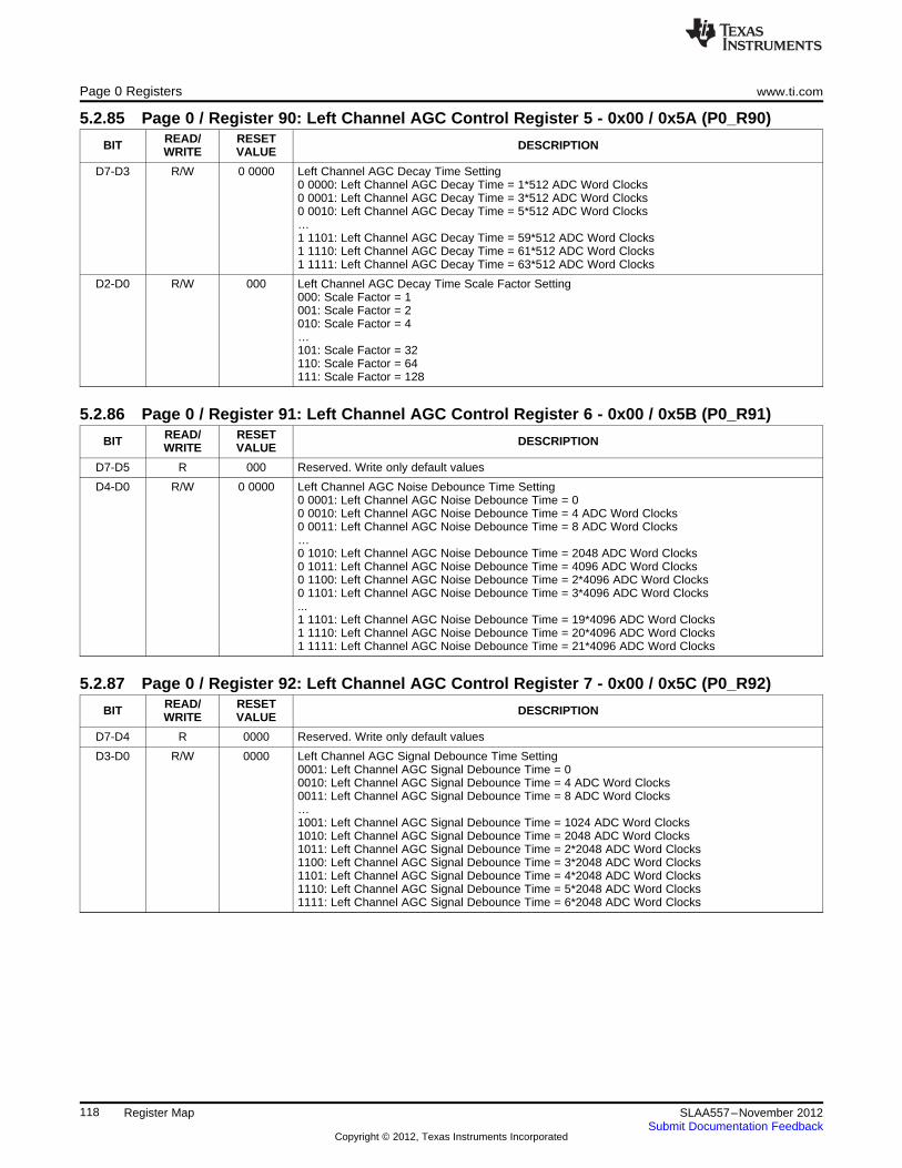
Page 0 Registers www.ti.com
5.2.85 Page 0 / Register 90: Left Channel AGC Control Register 5 - 0x00 / 0x5A (P0_R90)READ/ RESETBIT DESCRIPTIONWRITE VALUE
D7-D3 R/W 0 0000 Left Channel AGC Decay Time Setting0 0000: Left Channel AGC Decay Time = 1*512 ADC Word Clocks0 0001: Left Channel AGC Decay Time = 3*512 ADC Word Clocks0 0010: Left Channel AGC Decay Time = 5*512 ADC Word Clocks…1 1101: Left Channel AGC Decay Time = 59*512 ADC Word Clocks1 1110: Left Channel AGC Decay Time = 61*512 ADC Word Clocks1 1111: Left Channel AGC Decay Time = 63*512 ADC Word Clocks
D2-D0 R/W 000 Left Channel AGC Decay Time Scale Factor Setting000: Scale Factor = 1001: Scale Factor = 2010: Scale Factor = 4…101: Scale Factor = 32110: Scale Factor = 64111: Scale Factor = 128
5.2.86 Page 0 / Register 91: Left Channel AGC Control Register 6 - 0x00 / 0x5B (P0_R91)READ/ RESETBIT DESCRIPTIONWRITE VALUE
D7-D5 R 000 Reserved. Write only default values
D4-D0 R/W 0 0000 Left Channel AGC Noise Debounce Time Setting0 0001: Left Channel AGC Noise Debounce Time = 00 0010: Left Channel AGC Noise Debounce Time = 4 ADC Word Clocks0 0011: Left Channel AGC Noise Debounce Time = 8 ADC Word Clocks…0 1010: Left Channel AGC Noise Debounce Time = 2048 ADC Word Clocks0 1011: Left Channel AGC Noise Debounce Time = 4096 ADC Word Clocks0 1100: Left Channel AGC Noise Debounce Time = 2*4096 ADC Word Clocks0 1101: Left Channel AGC Noise Debounce Time = 3*4096 ADC Word Clocks...1 1101: Left Channel AGC Noise Debounce Time = 19*4096 ADC Word Clocks1 1110: Left Channel AGC Noise Debounce Time = 20*4096 ADC Word Clocks1 1111: Left Channel AGC Noise Debounce Time = 21*4096 ADC Word Clocks
5.2.87 Page 0 / Register 92: Left Channel AGC Control Register 7 - 0x00 / 0x5C (P0_R92)READ/ RESETBIT DESCRIPTIONWRITE VALUE
D7-D4 R 0000 Reserved. Write only default values
D3-D0 R/W 0000 Left Channel AGC Signal Debounce Time Setting0001: Left Channel AGC Signal Debounce Time = 00010: Left Channel AGC Signal Debounce Time = 4 ADC Word Clocks0011: Left Channel AGC Signal Debounce Time = 8 ADC Word Clocks…1001: Left Channel AGC Signal Debounce Time = 1024 ADC Word Clocks1010: Left Channel AGC Signal Debounce Time = 2048 ADC Word Clocks1011: Left Channel AGC Signal Debounce Time = 2*2048 ADC Word Clocks1100: Left Channel AGC Signal Debounce Time = 3*2048 ADC Word Clocks1101: Left Channel AGC Signal Debounce Time = 4*2048 ADC Word Clocks1110: Left Channel AGC Signal Debounce Time = 5*2048 ADC Word Clocks1111: Left Channel AGC Signal Debounce Time = 6*2048 ADC Word Clocks
118 Register Map SLAA557–November 2012Submit Documentation Feedback
Copyright © 2012, Texas Instruments Incorporated

www.ti.com Page 0 Registers
5.2.88 Page 0 / Register 93: Left Channel AGC Control Register 8 - 0x00 / 0x5D (P0_R93)READ/ RESETBIT DESCRIPTIONWRITE VALUE
D7-D0 R 0000 0000 Left Channel AGC Gain Flag1110 1000: Left Channel AGC Gain = -12.0dB1110 1001: Left Channel AGC Gain = -11.5dB1110 1010: Left Channel AGC Gain = -11.0dB…0000 0000: Left Channel AGC Gain = 0.0dB…0111 0010: Left Channel AGC Gain = 57.0dB0111 0011: Left Channel AGC Gain = 57.5dB0111 0100: Left Channel AGC Gain = 58.0dB
5.2.89 Page 0 / Register 94: Right Channel AGC Control Register 1 - 0x00 / 0x5E (P0_R94)READ/ RESETBIT DESCRIPTIONWRITE VALUE
D7 R/W 0 0: Right Channel AGC Disabled1: Right Channel AGC Enabled
D6-D4 R/W 000 Right Channel AGC Target Level Setting000: Right Channel AGC Target Level = -5.5dBFS001: Right Channel AGC Target Level = -8.0dBFS010: Right Channel AGC Target Level = -10.0dBFS011: Right Channel AGC Target Level = -12.0dBFS100: Right Channel AGC Target Level = -14.0dBFS101: Right Channel AGC Target Level = -17.0dBFS110: Right Channel AGC Target Level = -20.0dBFS111: Right Channel AGC Target Level = -24.0dBFS
D3-D2 R 00 Reserved. Write only default values
D1-D0 R/W 00 Right Channel AGC Gain Hysteresis Control00: Right Channel AGC Gain Hysteresis is disabled01: Right Channel AGC Gain Hysteresis is ±0.5dB10: Right Channel AGC Gain Hysteresis is ±1.0dB11: Right Channel AGC Gain Hysteresis is ±1.5dB
5.2.90 Page 0 / Register 95: Right Channel AGC Control Register 2 - 0x00 / 0x5F (P0_R95)READ/ RESETBIT DESCRIPTIONWRITE VALUE
D7-D6 R/W 00 Right Channel AGC Hysteresis Setting00: Right Channel AGC Hysteresis is 1.0dB01: Right Channel AGC Hysteresis is 2.0dB10: Right Channel AGC Hysteresis is 4.0dB11: Right Channel AGC Hysteresis is disabled
D5-D1 R/W 0 0000 Right Channel AGC Noise Threshold0 0000: Right Channel AGC Noise Gate disabled0 0001: Right Channel AGC Noise Threshold is -30dB0 0010: Right Channel AGC Noise Threshold is -32dB0 0011: Right Channel AGC Noise Threshold is -34dB…1 1101: Right Channel AGC Noise Threshold is -86dB1 1110: Right Channel AGC Noise Threshold is -88dB1 1111: Right Channel AGC Noise Threshold is -90dB
D0 R 0 Reserved. Write only default value
5.2.91 Page 0 / Register 96: Right Channel AGC Control Register 3 - 0x00 / 0x60 (P0_R96)READ/ RESETBIT DESCRIPTIONWRITE VALUE
D7 R 0 Reserved. Write only default value
119SLAA557–November 2012 Register MapSubmit Documentation Feedback
Copyright © 2012, Texas Instruments Incorporated

Page 0 Registers www.ti.com
Page 0 / Register 96: Right Channel AGC Control Register 3 - 0x00 / 0x60 (P0_R96) (continued)
READ/ RESETBIT DESCRIPTIONWRITE VALUE
D6-D0 R/W 111 1111 Right Channel AGC Maximum Gain Setting000 0000: Right Channel AGC Maximum Gain = 0.0dB000 0001: Right Channel AGC Maximum Gain = 0.5dB000 0010: Right Channel AGC Maximum Gain = 1.0dB…111 0011: Right Channel AGC Maximum Gain = 57.5dB111 0100: Right Channel AGC Maximum Gain = 58.0dB111 0101-111 1111: not recommended for usage, Right Channel AGC Maximum Gain = 58.0dB
5.2.92 Page 0 / Register 97: Right Channel AGC Control Register 4 - 0x00 / 0x61 (P0_R97)READ/ RESETBIT DESCRIPTIONWRITE VALUE
D7-D3 R/W 0 0000 Right Channel AGC Attack Time Setting0 0000: Right Channel AGC Attack Time = 1*32 ADC Word Clocks0 0001: Right Channel AGC Attack Time = 3*32 ADC Word Clocks0 0010: Right Channel AGC Attack Time = 5*32 ADC Word Clocks…1 1101: Right Channel AGC Attack Time = 59*32 ADC Word Clocks1 1110: Right Channel AGC Attack Time = 61*32 ADC Word Clocks1 1111: Right Channel AGC Attack Time = 63*32 ADC Word Clocks
D2-D0 R/W 000 Right Channel AGC Attack Time Scale Factor Setting000: Scale Factor = 1001: Scale Factor = 2010: Scale Factor = 4…101: Scale Factor = 32110: Scale Factor = 64111: Scale Factor = 128
5.2.93 Page 0 / Register 98: Right Channel AGC Control Register 5 - 0x00 / 0x62 (P0_R98)READ/ RESETBIT DESCRIPTIONWRITE VALUE
D7-D3 R/W 0 0000 Right Channel AGC Decay Time Setting0 0000: Right Channel AGC Decay Time = 1*512 ADC Word Clocks0 0001: Right Channel AGC Decay Time = 3*512 ADC Word Clocks0 0010: Right Channel AGC Decay Time = 5*512 ADC Word Clocks…1 1101: Right Channel AGC Decay Time = 59*512 ADC Word Clocks1 1110: Right Channel AGC Decay Time = 61*512 ADC Word Clocks1 1111: Right Channel AGC Decay Time = 63*512 ADC Word Clocks
D2-D0 R/W 000 Right Channel AGC Decay Time Scale Factor Setting000: Scale Factor = 1001: Scale Factor = 2010: Scale Factor = 4…101: Scale Factor = 32110: Scale Factor = 64111: Scale Factor = 128
5.2.94 Page 0 / Register 99: Right Channel AGC Control Register 6 - 0x00 / 0x63 (P0_R99)READ/ RESETBIT DESCRIPTIONWRITE VALUE
D7-D5 R 000 Reserved. Write only default values
120 Register Map SLAA557–November 2012Submit Documentation Feedback
Copyright © 2012, Texas Instruments Incorporated
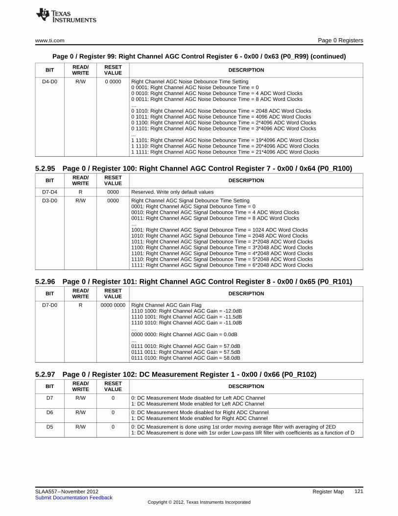
www.ti.com Page 0 Registers
Page 0 / Register 99: Right Channel AGC Control Register 6 - 0x00 / 0x63 (P0_R99) (continued)
READ/ RESETBIT DESCRIPTIONWRITE VALUE
D4-D0 R/W 0 0000 Right Channel AGC Noise Debounce Time Setting0 0001: Right Channel AGC Noise Debounce Time = 00 0010: Right Channel AGC Noise Debounce Time = 4 ADC Word Clocks0 0011: Right Channel AGC Noise Debounce Time = 8 ADC Word Clocks…0 1010: Right Channel AGC Noise Debounce Time = 2048 ADC Word Clocks0 1011: Right Channel AGC Noise Debounce Time = 4096 ADC Word Clocks0 1100: Right Channel AGC Noise Debounce Time = 2*4096 ADC Word Clocks0 1101: Right Channel AGC Noise Debounce Time = 3*4096 ADC Word Clocks...1 1101: Right Channel AGC Noise Debounce Time = 19*4096 ADC Word Clocks1 1110: Right Channel AGC Noise Debounce Time = 20*4096 ADC Word Clocks1 1111: Right Channel AGC Noise Debounce Time = 21*4096 ADC Word Clocks
5.2.95 Page 0 / Register 100: Right Channel AGC Control Register 7 - 0x00 / 0x64 (P0_R100)READ/ RESETBIT DESCRIPTIONWRITE VALUE
D7-D4 R 0000 Reserved. Write only default values
D3-D0 R/W 0000 Right Channel AGC Signal Debounce Time Setting0001: Right Channel AGC Signal Debounce Time = 00010: Right Channel AGC Signal Debounce Time = 4 ADC Word Clocks0011: Right Channel AGC Signal Debounce Time = 8 ADC Word Clocks…1001: Right Channel AGC Signal Debounce Time = 1024 ADC Word Clocks1010: Right Channel AGC Signal Debounce Time = 2048 ADC Word Clocks1011: Right Channel AGC Signal Debounce Time = 2*2048 ADC Word Clocks1100: Right Channel AGC Signal Debounce Time = 3*2048 ADC Word Clocks1101: Right Channel AGC Signal Debounce Time = 4*2048 ADC Word Clocks1110: Right Channel AGC Signal Debounce Time = 5*2048 ADC Word Clocks1111: Right Channel AGC Signal Debounce Time = 6*2048 ADC Word Clocks
5.2.96 Page 0 / Register 101: Right Channel AGC Control Register 8 - 0x00 / 0x65 (P0_R101)READ/ RESETBIT DESCRIPTIONWRITE VALUE
D7-D0 R 0000 0000 Right Channel AGC Gain Flag1110 1000: Right Channel AGC Gain = -12.0dB1110 1001: Right Channel AGC Gain = -11.5dB1110 1010: Right Channel AGC Gain = -11.0dB…0000 0000: Right Channel AGC Gain = 0.0dB…0111 0010: Right Channel AGC Gain = 57.0dB0111 0011: Right Channel AGC Gain = 57.5dB0111 0100: Right Channel AGC Gain = 58.0dB
5.2.97 Page 0 / Register 102: DC Measurement Register 1 - 0x00 / 0x66 (P0_R102)READ/ RESETBIT DESCRIPTIONWRITE VALUE
D7 R/W 0 0: DC Measurement Mode disabled for Left ADC Channel1: DC Measurement Mode enabled for Left ADC Channel
D6 R/W 0 0: DC Measurement Mode disabled for Right ADC Channel1: DC Measurement Mode enabled for Right ADC Channel
D5 R/W 0 0: DC Measurement is done using 1st order moving average filter with averaging of 2ED1: DC Measurement is done with 1sr order Low-pass IIR filter with coefficients as a function of D
121SLAA557–November 2012 Register MapSubmit Documentation Feedback
Copyright © 2012, Texas Instruments Incorporated

Page 0 Registers www.ti.com
Page 0 / Register 102: DC Measurement Register 1 - 0x00 / 0x66 (P0_R102) (continued)
READ/ RESETBIT DESCRIPTIONWRITE VALUE
D4-D0 R/W 0 0000 DC Measurement D setting0 0000: Reserved. Do not use0 0001: DC Measurement D parameter = 10 0010: DC Measurement D parameter = 2..1 0011: DC Measurement D parameter = 191 0100: DC Measurement D parameter = 201 0101-1 1111: Reserved. Do not use
5.2.98 Page 0 / Register 103: DC Measurement Register 2 - 0x00 / 0x67 (P0_R103)READ/ RESETBIT DESCRIPTIONWRITE VALUE
D7 R 0 Reserved. Write only default values
D6 R/W 0 0: Left and Right Channel DC measurement result update enabled1: Left and Right Channel DC measurement result update disabled; new results will be updatedwhile old results are being read
D5 R/W 0 0: For IIR based DC measurement, measurement value is the instantaneous output of IIR filter1: For IIR based DC measurement, the measurement value is updated before periodic clearing ofIIR filter
D4-D0 R/W 0 0000 IIR based DC Measurement, averaging time setting0 0000: Infinite average is used0 0001: Averaging time is 2E1 ADC Modulator clocks0 0010: Averaging time is 2E2 ADC Modulator clocks…1 0011: Averaging time is 2E19 ADC Modulator clocks1 0100: Averaging time is 2E20 ADC Modulator clocks1 0101-1 1111: Reserved. Do not use
5.2.99 Page 0 / Register 104: Left Channel DC Measurement Output Register 1 - 0x00 / 0x68(P0_R104)
READ/ RESETBIT DESCRIPTIONWRITE VALUE
D7-D0 R 0000 0000 Left Channel DC Measurement Output (23:16)
5.2.100 Page 0 / Register 105: Left Channel DC Measurement Output Register 2 - 0x00 / 0x69(P0_R105)
READ/ RESETBIT DESCRIPTIONWRITE VALUE
D7-D0 R 0000 0000 Left Channel DC Measurement Output (15:8)
5.2.101 Page 0 / Register 106: Left Channel DC Measurement Output Register 3 - 0x00 / 0x6A(P0_R106)
READ/ RESETBIT DESCRIPTIONWRITE VALUE
D7-D0 R 0000 0000 Left Channel DC Measurement Output (7:0)
5.2.102 Page 0 / Register 107: Right Channel DC Measurement Output Register 1 - 0x00 / 0x6B(P0_R107)
READ/ RESETBIT DESCRIPTIONWRITE VALUE
D7-D0 R 0000 0000 Right Channel DC Measurement Output (23:16)
5.2.103 Page 0 / Register 108: Right Channel DC Measurement Output Register 2 - 0x00 / 0x6C
122 Register Map SLAA557–November 2012Submit Documentation Feedback
Copyright © 2012, Texas Instruments Incorporated
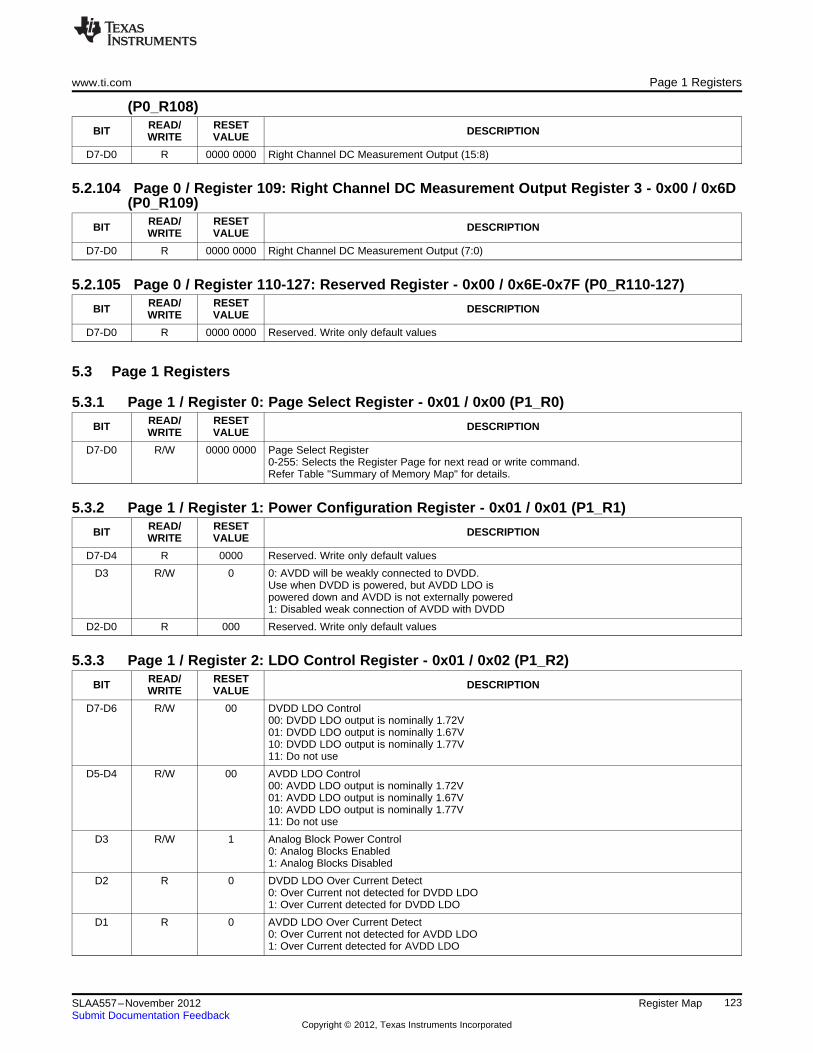
www.ti.com Page 1 Registers
(P0_R108)READ/ RESETBIT DESCRIPTIONWRITE VALUE
D7-D0 R 0000 0000 Right Channel DC Measurement Output (15:8)
5.2.104 Page 0 / Register 109: Right Channel DC Measurement Output Register 3 - 0x00 / 0x6D(P0_R109)
READ/ RESETBIT DESCRIPTIONWRITE VALUE
D7-D0 R 0000 0000 Right Channel DC Measurement Output (7:0)
5.2.105 Page 0 / Register 110-127: Reserved Register - 0x00 / 0x6E-0x7F (P0_R110-127)READ/ RESETBIT DESCRIPTIONWRITE VALUE
D7-D0 R 0000 0000 Reserved. Write only default values
5.3 Page 1 Registers
5.3.1 Page 1 / Register 0: Page Select Register - 0x01 / 0x00 (P1_R0)READ/ RESETBIT DESCRIPTIONWRITE VALUE
D7-D0 R/W 0000 0000 Page Select Register0-255: Selects the Register Page for next read or write command.Refer Table "Summary of Memory Map" for details.
5.3.2 Page 1 / Register 1: Power Configuration Register - 0x01 / 0x01 (P1_R1)READ/ RESETBIT DESCRIPTIONWRITE VALUE
D7-D4 R 0000 Reserved. Write only default values
D3 R/W 0 0: AVDD will be weakly connected to DVDD.Use when DVDD is powered, but AVDD LDO ispowered down and AVDD is not externally powered1: Disabled weak connection of AVDD with DVDD
D2-D0 R 000 Reserved. Write only default values
5.3.3 Page 1 / Register 2: LDO Control Register - 0x01 / 0x02 (P1_R2)READ/ RESETBIT DESCRIPTIONWRITE VALUE
D7-D6 R/W 00 DVDD LDO Control00: DVDD LDO output is nominally 1.72V01: DVDD LDO output is nominally 1.67V10: DVDD LDO output is nominally 1.77V11: Do not use
D5-D4 R/W 00 AVDD LDO Control00: AVDD LDO output is nominally 1.72V01: AVDD LDO output is nominally 1.67V10: AVDD LDO output is nominally 1.77V11: Do not use
D3 R/W 1 Analog Block Power Control0: Analog Blocks Enabled1: Analog Blocks Disabled
D2 R 0 DVDD LDO Over Current Detect0: Over Current not detected for DVDD LDO1: Over Current detected for DVDD LDO
D1 R 0 AVDD LDO Over Current Detect0: Over Current not detected for AVDD LDO1: Over Current detected for AVDD LDO
123SLAA557–November 2012 Register MapSubmit Documentation Feedback
Copyright © 2012, Texas Instruments Incorporated

Page 1 Registers www.ti.com
Page 1 / Register 2: LDO Control Register - 0x01 / 0x02 (P1_R2) (continued)
READ/ RESETBIT DESCRIPTIONWRITE VALUE
D0 R/W 0 AVDD LDO Power Control0: AVDD LDO Powered down1: AVDD LDO Powered up
5.3.4 Page 1 / Register 3: Playback Configuration Register 1 - 0x01 / 0x03 (P1_R3)READ/ RESETBIT DESCRIPTIONWRITE VALUE
D7-D6 R/W 00 00: Left DAC routing to HPL uses Class-AB driver01-10: Reserved. Do not use11: Left DAC routing to HPL uses Class-D driver
D5 R 0 Reserved. Write only default values
D4-D2 R/W 000 Left DAC PTM Control000: Left DAC in mode PTM_P3, PTM_P4001: Left DAC in mode PTM_P2010: Left DAC in mode PTM_P1011-111: Reserved. Do not use
D1-D0 R 00 Reserved. Write only default values
5.3.5 Page 1 / Register 4: Playback Configuration Register 2 - 0x01 / 0x04 (P1_R4)READ/ RESETBIT DESCRIPTIONWRITE VALUE
D7-D6 R/W 00 00: Right DAC routing to HPL uses Class-AB driver01-10: Reserved. Do not use11: Right DAC routing to HPL uses Class-D driver
D5 R 0 Reserved. Write only default values
D4-D2 R/W 000 Right DAC PTM Control000: Right DAC in mode PTM_P3, PTM_P4001: Right DAC in mode PTM_P2010: Right DAC in mode PTM_P1011-111: Reserved. Do not use
D1-D0 R 00 Reserved. Write only default values
5.3.6 Page 1 / Register 5-8: Reserved Register - 0x01 / 0x05-0x08 (P1_R5-8)READ/ RESETBIT DESCRIPTIONWRITE VALUE
D7-D0 R 0000 0000 Reserved. Write only default values
5.3.7 Page 1 / Register 9: Output Driver Power Control Register - 0x01 / 0x09 (P1_R9)READ/ RESETBIT DESCRIPTIONWRITE VALUE
D7-D6 R 00 Reserved. Write only default value
D5 R/W 0 0: HPL is powered down1: HPL is powered up
D4 R/W 0 0: HPR is powered down1: HPR is powered up
D3 R/W 0 0: LOL is powered down1: LOL is powered up
D2 R/W 0 0: LOR is powered down1: LOR is powered up
D1 R/W 0 0: Left Mixer Amplifier (MAL) is powered down1: Left Mixer Amplifier (MAL) is powered up
D0 R/W 0 0: Right Mixer Amplifier (MAR) is powered down1: Right Mixer Amplifier (MAR) is powered up
124 Register Map SLAA557–November 2012Submit Documentation Feedback
Copyright © 2012, Texas Instruments Incorporated
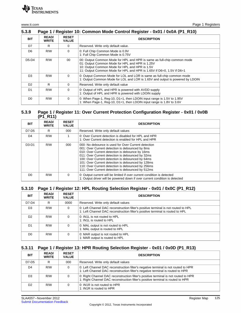
www.ti.com Page 1 Registers
5.3.8 Page 1 / Register 10: Common Mode Control Register - 0x01 / 0x0A (P1_R10)READ/ RESETBIT DESCRIPTIONWRITE VALUE
D7 R 0 Reserved. Write only default value.
D6 R/W 0 0: Full Chip Common Mode is 0.9V1: Full Chip Common Mode is 0.75V
D5-D4 R/W 00 00: Output Common Mode for HPL and HPR is same as full-chip common mode01: Output Common Mode for HPL and HPR is 1.25V10: Output Common Mode for HPL and HPR is 1.5V11: Output Common Mode for HPL and HPR is 1.65V if D6=0, 1.5V if D6=1
D3 R/W 0 0: Output Common Mode for LOL and LOR is same as full-chip common mode1: Output Common Mode for LOL and LOR is 1.65V and output is powered by LDOIN
D2 R 0 Reserved. Write only default value
D1 R/W 0 0: Output of HPL and HPR is powered with AVDD supply1: Output of HPL and HPR is powered with LDOIN supply
D0 R/W 0 0: When Page-1, Reg-10, D1=1, then LDOIN input range is 1.5V to 1.95V1: When Page-1, Reg-10, D1=1, then LDOIN input range is 1.8V to 3.6V
5.3.9 Page 1 / Register 11: Over Current Protection Configuration Register - 0x01 / 0x0B(P1_R11)
READ/ RESETBIT DESCRIPTIONWRITE VALUE
D7-D5 R 000 Reserved. Write only default values
D4 R/W 1 0: Over Current detection is disabled for HPL and HPR1: Over Current detection is enabled for HPL and HPR
D3-D1 R/W 000 000: No debounce is used for Over Current detection001: Over Current detection is debounced by 8ms010: Over Current detection is debounce by 16ms011: Over Current detection is debounced by 32ms100: Over Current detection is debounced by 64ms101: Over Current detection is debounced by 128ms110: Over Current detection is debounced by 256ms111: Over Current detection is debounced by 512ms
D0 R/W 0 0: Output current will be limited if over current condition is detected1: Output driver will be powered down if over current condition is detected
5.3.10 Page 1 / Register 12: HPL Routing Selection Register - 0x01 / 0x0C (P1_R12)READ/ RESETBIT DESCRIPTIONWRITE VALUE
D7-D4 R 0000 Reserved. Write only default values
D3 R/W 0 0: Left Channel DAC reconstruction filter's positive terminal is not routed to HPL1: Left Channel DAC reconstruction filter's positive terminal is routed to HPL
D2 R/W 0 0: IN1L is not routed to HPL1: IN1L is routed to HPL
D1 R/W 0 0: MAL output is not routed to HPL1: MAL output is routed to HPL
D0 R/W 0 0: MAR output is not routed to HPL1: MAR output is routed to HPL
5.3.11 Page 1 / Register 13: HPR Routing Selection Register - 0x01 / 0x0D (P1_R13)READ/ RESETBIT DESCRIPTIONWRITE VALUE
D7-D5 R 000 Reserved. Write only default values
D4 R/W 0 0: Left Channel DAC reconstruction filter's negative terminal is not routed to HPR1: Left Channel DAC reconstruction filter's negative terminal is routed to HPR
D3 R/W 0 0: Right Channel DAC reconstruction filter's positive terminal is not routed to HPR1: Right Channel DAC reconstruction filter's positive terminal is routed to HPR
D2 R/W 0 0: IN1R is not routed to HPR1: IN1R is routed to HPR
125SLAA557–November 2012 Register MapSubmit Documentation Feedback
Copyright © 2012, Texas Instruments Incorporated

Page 1 Registers www.ti.com
Page 1 / Register 13: HPR Routing Selection Register - 0x01 / 0x0D (P1_R13) (continued)
READ/ RESETBIT DESCRIPTIONWRITE VALUE
D1 R/W 0 0: MAR output is not routed to HPR1: MAR output is routed to HPR
D0 R/W 0 0: HPL output is not routed to HPR1: HPL output is routed to HPR (use when HPL and HPR output is powered by AVDD)
5.3.12 Page 1 / Register 14: LOL Routing Selection Register - 0x01 / 0x0E (P1_R14)READ/ RESETBIT DESCRIPTIONWRITE VALUE
D7-D5 R 000 Reserved. Write only default values
D4 R/W 0 0: Right Channel DAC reconstruction filter's negative terminal is not routed to LOL1: Right Channel DAC reconstruction filter's negative terminal is routed to LOL
D3 R/W 0 0: Left Channel DAC reconstruction filter output is not routed to LOL1: Left Channel DAC reconstruction filter output is routed to LOL
D2 R 0 Reserved. Write only default value.
D1 R/W 0 0: MAL output is not routed to LOL1: MAL output is routed to LOL
D0 R/W 0 0: LOR output is not routed to LOL1: LOR output is routed to LOL(use when LOL and LOR output is powered by AVDD)
5.3.13 Page 1 / Register 15: LOR Routing Selection Register - 0x01 / 0x0F (P1_R15)READ/ RESETBIT DESCRIPTIONWRITE VALUE
D7-D4 R 0000 Reserved. Write only default values
D3 R/W 0 0: Right Channel DAC reconstruction filter output is not routed to LOR1: Right Channel DAC reconstruction filter output is routed to LOR
D2 R 0 Reserved. Write only default value.
D1 R/W 0 0: MAR output is not routed to LOR1: MAR output is routed to LOR
D0 R 0 Reserved. Write only default value.
5.3.14 Page 1 / Register 16: HPL Driver Gain Setting Register - 0x01 / 0x10 (P1_R16)READ/ RESETBIT DESCRIPTIONWRITE VALUE
D7 R 0 Reserved. Write only default value.
D6 R/W 1 0: HPL driver is not muted1: HPL driver is muted
D5-D0 R/W 00 0000 10 0000-11 1001: Reserved. Do not use11 1010: HPL driver gain is -6dB(Note: It is not possible to mute HPR while programmed to -6dB)11 1011: HPL driver gain is -5dB11 1100: HPL driver gain is -4dB…00 0000: HPL driver gain is 0dB...01 1011: HPL driver gain is 27dB01 1100: HPL driver gain is 28dB01 1101: HPL driver gain is 29dB01 1110-01 1111: Reserved. Do not useNote: These gains are not valid while using the driver in Class-D mode
5.3.15 Page 1 / Register 17: HPR Driver Gain Setting Register - 0x01 / 0x11 (P1_R17)READ/ RESETBIT DESCRIPTIONWRITE VALUE
D7 R 0 Reserved. Write only default value.
126 Register Map SLAA557–November 2012Submit Documentation Feedback
Copyright © 2012, Texas Instruments Incorporated
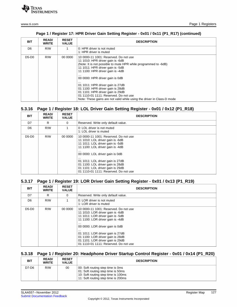
www.ti.com Page 1 Registers
Page 1 / Register 17: HPR Driver Gain Setting Register - 0x01 / 0x11 (P1_R17) (continued)
READ/ RESETBIT DESCRIPTIONWRITE VALUE
D6 R/W 1 0: HPR driver is not muted1: HPR driver is muted
D5-D0 R/W 00 0000 10 0000-11 1001: Reserved. Do not use11 1010: HPR driver gain is -6dB(Note: It is not possible to mute HPR while programmed to -6dB)11 1011: HPR driver gain is -5dB11 1100: HPR driver gain is -4dB…00 0000: HPR driver gain is 0dB...01 1011: HPR driver gain is 27dB01 1100: HPR driver gain is 28dB01 1101: HPR driver gain is 29dB01 1110-01 1111: Reserved. Do not useNote: These gains are not valid while using the driver in Class-D mode
5.3.16 Page 1 / Register 18: LOL Driver Gain Setting Register - 0x01 / 0x12 (P1_R18)READ/ RESETBIT DESCRIPTIONWRITE VALUE
D7 R 0 Reserved. Write only default value.
D6 R/W 1 0: LOL driver is not muted1: LOL driver is muted
D5-D0 R/W 00 0000 10 0000-11 1001: Reserved. Do not use11 1010: LOL driver gain is -6dB11 1011: LOL driver gain is -5dB11 1100: LOL driver gain is -4dB…00 0000: LOL driver gain is 0dB...01 1011: LOL driver gain is 27dB01 1100: LOL driver gain is 28dB01 1101: LOL driver gain is 29dB01 1110-01 1111: Reserved. Do not use
5.3.17 Page 1 / Register 19: LOR Driver Gain Setting Register - 0x01 / 0x13 (P1_R19)READ/ RESETBIT DESCRIPTIONWRITE VALUE
D7 R 0 Reserved. Write only default value.
D6 R/W 1 0: LOR driver is not muted1: LOR driver is muted
D5-D0 R/W 00 0000 10 0000-11 1001: Reserved. Do not use11 1010: LOR driver gain is -6dB11 1011: LOR driver gain is -5dB11 1100: LOR driver gain is -4dB…00 0000: LOR driver gain is 0dB...01 1011: LOR driver gain is 27dB01 1100: LOR driver gain is 28dB01 1101: LOR driver gain is 29dB01 1110-01 1111: Reserved. Do not use
5.3.18 Page 1 / Register 20: Headphone Driver Startup Control Register - 0x01 / 0x14 (P1_R20)READ/ RESETBIT DESCRIPTIONWRITE VALUE
D7-D6 R/W 00 00: Soft routing step time is 0ms01: Soft routing step time is 50ms10: Soft routing step time is 100ms11: Soft routing step time is 200ms
127SLAA557–November 2012 Register MapSubmit Documentation Feedback
Copyright © 2012, Texas Instruments Incorporated

Page 1 Registers www.ti.com
Page 1 / Register 20: Headphone Driver Startup Control Register - 0x01 / 0x14 (P1_R20) (continued)
READ/ RESETBIT DESCRIPTIONWRITE VALUE
D5-D2 R/W 0000 0000: Slow power up of headphone amp's is disabled0001: Headphone ramps power up slowly in 0.5 time constants0010: Headphone ramps power up slowly in 0.625 time constants0011; Headphone ramps power up slowly in 0.725 time constants0100: Headphone ramps power up slowly in 0.875 time constants0101: Headphone ramps power up slowly in 1.0 time constants0110: Headphone ramps power up slowly in 2.0 time constants0111: Headphone ramps power up slowly in 3.0 time constants1000: Headphone ramps power up slowly in 4.0 time constants1001: Headphone ramps power up slowly in 5.0 time constants1010: Headphone ramps power up slowly in 6.0 time constants1011: Headphone ramps power up slowly in 7.0 time constants1100: Headphone ramps power up slowly in 8.0 time constants1101: Headphone ramps power up slowly in 16.0 time constants ( do not use for Rchg=25K)1110: Headphone ramps power up slowly in 24.0 time constants (do not use for Rchg=25K)1111: Headphone ramps power up slowly in 32.0 time constants (do not use for Rchg=25K)Note: Time constants assume 47uF decoupling cap
D1-D0 R/W 00 00: Headphone ramps power up time is determined with 25k resistance01: Headphone ramps power up time is determined with 6k resistance10: Headphone ramps power up time is determined with 2k resistance11: Reserved. Do not use
5.3.19 Page 1 / Register 21: Reserved Register - 0x01 / 0x15 (P1_R21)READ/ RESETBIT DESCRIPTIONWRITE VALUE
D7-D0 R 0000 0000 Reserved. Write only default values
5.3.20 Page 1 / Register 22: IN1L to HPL Volume Control Register - 0x01 / 0x16 (P1_R22)READ/ RESETBIT DESCRIPTIONWRITE VALUE
D7 R 0 Reserved. Write only default value.
128 Register Map SLAA557–November 2012Submit Documentation Feedback
Copyright © 2012, Texas Instruments Incorporated

www.ti.com Page 1 Registers
Page 1 / Register 22: IN1L to HPL Volume Control Register - 0x01 / 0x16 (P1_R22) (continued)
READ/ RESETBIT DESCRIPTIONWRITE VALUE
D6-D0 R/W 000 0000 IN1L to HPL Volume Control000 0000: Volume Control = 0.0dB000 0001: Volume Control = -0.5dB000 0010: Volume Control = -1.0dB000 0011: Volume Control = -1.5dB000 0100: Volume Control = -2.0dB000 0101: Volume Control = -2.5dB000 0110: Volume Control = -3.0dB000 0111: Volume Control = -3.5dB000 1000: Volume Control = -4.0dB000 1001: Volume Control = -4.5dB000 1010: Volume Control = -5.0dB000 1011: Volume Control = -5.5dB000 1100: Volume Control = -6.0dB000 1101: Volume Control = -6.5dB000 1110: Volume Control = -7.0dB000 1111: Volume Control = -7.5dB001 0000: Volume Control = -8.0dB001 0001: Volume Control = -8.5dB001 0010: Volume Control = -9.0dB001 0011: Volume Control = -9.5dB001 0100: Volume Control = -10.0dB001 0101: Volume Control = -10.5dB001 0110: Volume Control = -11.0dB001 0111: Volume Control = -11.5dB001 1000: Volume Control = -12.0dB001 1001: Volume Control = -12.5dB001 1010: Volume Control = -13.0dB001 1011: Volume Control = -13.5dB001 1100: Volume Control = -14.0dB001 1101: Volume Control = -14.5dB001 1110: Volume Control = -15.0dB001 1111: Volume Control = -15.5dB010 0000: Volume Control = -16.0dB010 0001: Volume Control = -16.5dB010 0010: Volume Control = -17.1dB010 0011: Volume Control = -17.5dB010 0100: Volume Control = -18.1dB010 0101: Volume Control = -18.6dB010 0110: Volume Control = -19.1dB010 0111: Volume Control = -19.6dB010 1000: Volume Control = -20.1dB010 1001: Volume Control = -20.6dB010 1010: Volume Control = -21.1dB010 1011: Volume Control = -21.6dB010 1100: Volume Control = -22.1dB010 1101: Volume Control = -22.6dB010 1110: Volume Control = -23.1dB010 1111: Volume Control = -23.6dB011 0000: Volume Control = -24.1dB011 0001: Volume Control = -24.6dB011 0010: Volume Control = -25.1dB011 0011: Volume Control = -25.6dB011 0100: Volume Control = -26.1dB011 0101: Volume Control = -26.6dB011 0110: Volume Control = -27.1dB011 0111: Volume Control = -27.6dB011 1000: Volume Control = -28.1dB011 1001: Volume Control = -28.6dB011 1010: Volume Control = -29.1dB011 1011: Volume Control = -29.6dB011 1100: Volume Control = -30.1dB011 1101: Volume Control = -30.6dB011 1110: Volume Control = -31.1dB011 1111: Volume Control = -31.6dB100 0000: Volume Control = -32.1dB100 0001:Volume Control = -32.6dB100 0010: Volume Control = -33.1dB
129SLAA557–November 2012 Register MapSubmit Documentation Feedback
Copyright © 2012, Texas Instruments Incorporated

Page 1 Registers www.ti.com
Page 1 / Register 22: IN1L to HPL Volume Control Register - 0x01 / 0x16 (P1_R22) (continued)
READ/ RESETBIT DESCRIPTIONWRITE VALUE
100 0011: Volume Control = -33.6dB100 0100: Volume Control = -34.1dB100 0101: Volume Control = -34.6dB100 0110: Volume Control = -35.2dB100 0111: Volume Control = -35.7dB100 1000: Volume Control = -36.2dB100 1001: Volume Control = -36.7dB100 1010: Volume Control = -37.2dB100 1011:Volume Control = -37.7dB100 1100: Volume Control = -38.2dB100 1101: Volume Control = -38.7dB100 1110: Volume Control = -39.2dB100 1111: Volume Control = -39.7dB101 0000: Volume Control = -40.2dB101 0001: Volume Control = -40.7dB101 0010: Volume Control = -41.2dB101 0011: Volume Control = -41.7dB101 0100: Volume Control = -42.1dB101 0101: Volume Control = -42.7dB101 0110: Volume Control = -43.2dB101 0111: Volume Control = -43.8dB101 1000: Volume Control = -44.3dB101 1001: Volume Control = -44.8dB101 1010: Volume Control = -45.2dB101 1011: Volume Control = -45.8dB101 1100: Volume Control = -46.2dB101 1101: Volume Control = -46.7dB101 1110: Volume Control = -47.4dB101 1111: Volume Control = -47.9dB110 0000: Volume Control = -48.2dB110 0001: Volume Control = -48.7dB110 0010: Volume Control = -49.3dB110 0011: Volume Control = -50.0dB110 0100: Volume Control = -50.3dB110 0101: Volume Control = -51.0dB110 0110: Volume Control = -51.4dB110 0111: Volume Control = -51.8dB110 1000: Volume Control = -52.3dB110 1001: Volume Control = -52.7dB110 1010: Volume Control = -53.7dB110 1011: Volume Control = -54.2dB110 1100: Volume Control = -55.4dB110 1101: Volume Control = -56.7dB110 1110: Volume Control = -58.3dB110 1111: Volume Control = -60.2dB111 0000: Volume Control = -62.7dB111 0001: Volume Control = -64.3dB111 0010: Volume Control = -66.2dB111 0011: Volume Control = -68.7dB111 0100: Volume Control = -72.3dB111 0101: Volume Control = MUTE111 0110-111 1111: Reserved. Do not use
5.3.21 Page 1 / Register 23: IN1R to HPR Volume Control Register - 0x01 / 0x17 (P1_R23)READ/ RESETBIT DESCRIPTIONWRITE VALUE
D7 R 0 Reserved. Write only default value
130 Register Map SLAA557–November 2012Submit Documentation Feedback
Copyright © 2012, Texas Instruments Incorporated

www.ti.com Page 1 Registers
Page 1 / Register 23: IN1R to HPR Volume Control Register - 0x01 / 0x17 (P1_R23) (continued)
READ/ RESETBIT DESCRIPTIONWRITE VALUE
D6-D0 R/W 000 0000 IN1R to HPR Volume Control000 0000: Volume Control = 0.0dB000 0001: Volume Control = -0.5dB000 0010: Volume Control = -1.0dB000 0011: Volume Control = -1.5dB000 0100: Volume Control = -2.0dB000 0101: Volume Control = -2.5dB000 0110: Volume Control = -3.0dB000 0111: Volume Control = -3.5dB000 1000: Volume Control = -4.0dB000 1001: Volume Control = -4.5dB000 1010: Volume Control = -5.0dB000 1011: Volume Control = -5.5dB000 1100: Volume Control = -6.0dB000 1101: Volume Control = -6.5dB000 1110: Volume Control = -7.0dB000 1111: Volume Control = -7.5dB001 0000: Volume Control = -8.0dB001 0001: Volume Control = -8.5dB001 0010: Volume Control = -9.0dB001 0011: Volume Control = -9.5dB001 0100: Volume Control = -10.0dB001 0101: Volume Control = -10.5dB001 0110: Volume Control = -11.0dB001 0111: Volume Control = -11.5dB001 1000: Volume Control = -12.0dB001 1001: Volume Control = -12.5dB001 1010: Volume Control = -13.0dB001 1011: Volume Control = -13.5dB001 1100: Volume Control = -14.0dB001 1101: Volume Control = -14.5dB001 1110: Volume Control = -15.0dB001 1111: Volume Control = -15.5dB010 0000: Volume Control = -16.0dB010 0001: Volume Control = -16.5dB010 0010: Volume Control = -17.1dB010 0011: Volume Control = -17.5dB010 0100: Volume Control = -18.1dB010 0101: Volume Control = -18.6dB010 0110: Volume Control = -19.1dB010 0111: Volume Control = -19.6dB010 1000: Volume Control = -20.1dB010 1001: Volume Control = -20.6dB010 1010: Volume Control = -21.1dB010 1011: Volume Control = -21.6dB010 1100: Volume Control = -22.1dB010 1101: Volume Control = -22.6dB010 1110: Volume Control = -23.1dB010 1111: Volume Control = -23.6dB011 0000: Volume Control = -24.1dB011 0001: Volume Control = -24.6dB011 0010: Volume Control = -25.1dB011 0011: Volume Control = -25.6dB011 0100: Volume Control = -26.1dB011 0101: Volume Control = -26.6dB011 0110: Volume Control = -27.1dB011 0111: Volume Control = -27.6dB011 1000: Volume Control = -28.1dB011 1001: Volume Control = -28.6dB011 1010: Volume Control = -29.1dB011 1011: Volume Control = -29.6dB011 1100: Volume Control = -30.1dB011 1101: Volume Control = -30.6dB011 1110: Volume Control = -31.1dB011 1111: Volume Control = -31.6dB100 0000: Volume Control = -32.1dB100 0001:Volume Control = -32.6dB100 0010: Volume Control = -33.1dB
131SLAA557–November 2012 Register MapSubmit Documentation Feedback
Copyright © 2012, Texas Instruments Incorporated

Page 1 Registers www.ti.com
Page 1 / Register 23: IN1R to HPR Volume Control Register - 0x01 / 0x17 (P1_R23) (continued)
READ/ RESETBIT DESCRIPTIONWRITE VALUE
100 0011: Volume Control = -33.6dB100 0100: Volume Control = -34.1dB100 0101: Volume Control = -34.6dB100 0110: Volume Control = -35.2dB100 0111: Volume Control = -35.7dB100 1000: Volume Control = -36.2dB100 1001: Volume Control = -36.7dB100 1010: Volume Control = -37.2dB100 1011:Volume Control = -37.7dB100 1100: Volume Control = -38.2dB100 1101: Volume Control = -38.7dB100 1110: Volume Control = -39.2dB100 1111: Volume Control = -39.7dB101 0000: Volume Control = -40.2dB101 0001: Volume Control = -40.7dB101 0010: Volume Control = -41.2dB101 0011: Volume Control = -41.7dB101 0100: Volume Control = -42.1dB101 0101: Volume Control = -42.7dB101 0110: Volume Control = -43.2dB101 0111: Volume Control = -43.8dB101 1000: Volume Control = -44.3dB101 1001: Volume Control = -44.8dB101 1010: Volume Control = -45.2dB101 1011: Volume Control = -45.8dB101 1100: Volume Control = -46.2dB101 1101: Volume Control = -46.7dB101 1110: Volume Control = -47.4dB101 1111: Volume Control = -47.9dB110 0000: Volume Control = -48.2dB110 0001: Volume Control = -48.7dB110 0010: Volume Control = -49.3dB110 0011: Volume Control = -50.0dB110 0100: Volume Control = -50.3dB110 0101: Volume Control = -51.0dB110 0110: Volume Control = -51.4dB110 0111: Volume Control = -51.8dB110 1000: Volume Control = -52.3dB110 1001: Volume Control = -52.7dB110 1010: Volume Control = -53.7dB110 1011: Volume Control = -54.2dB110 1100: Volume Control = -55.4dB110 1101: Volume Control = -56.7dB110 1110: Volume Control = -58.3dB110 1111: Volume Control = -60.2dB111 0000: Volume Control = -62.7dB111 0001: Volume Control = -64.3dB111 0010: Volume Control = -66.2dB111 0011: Volume Control = -68.7dB111 0100: Volume Control = -72.3dB111 0101: Volume Control = MUTE111 0110-111 1111: Reserved. Do not use
5.3.22 Page 1 / Register 24: Mixer Amplifier Left Volume Control Register - 0x01 / 0x18(P1_R24)
READ/ RESETBIT DESCRIPTIONWRITE VALUE
D7-D6 R 00 Reserved. Write only default values
132 Register Map SLAA557–November 2012Submit Documentation Feedback
Copyright © 2012, Texas Instruments Incorporated

www.ti.com Page 1 Registers
Page 1 / Register 24: Mixer Amplifier Left Volume Control Register - 0x01 / 0x18 (P1_R24) (continued)
READ/ RESETBIT DESCRIPTIONWRITE VALUE
D5-D0 R/W 00 0000 Mixer Amplifier Left Volume Control00 0000: Volume Control = 0.0dB00 0001: Volume Control = -0.4dB00 0010: Volume Control = -0.9dB00 0011: Volume Control = -1.3dB00 0100: Volume Control = -1.8dB00 0101: Volume Control = -2.3dB00 0110: Volume Control = -2.9dB00 0111: Volume Control = -3.3dB00 1000: Volume Control = -3.9dB00 1001: Volume Control = -4.3dB00 1010: Volume Control = -4.8dB00 1011: Volume Control = -5.2dB00 1100: Volume Control = -5.8dB00 1101: Volume Control = -6.3dB00 1110: Volume Control = -6.6dB00 1111: Volume Control = -7.2dB01 0000: Volume Control = -7.8dB01 0001: Volume Control = -8.2dB01 0010: Volume Control = -8.5dB01 0011: Volume Control = -9.3dB01 0100: Volume Control = -9.7dB01 0101: Volume Control = -10.1dB01 0110: Volume Control = -10.6dB01 0111: Volume Control = -11.0dB01 1000: Volume Control = -11.5dB01 1001: Volume Control = -12.0dB01 1010: Volume Control = -12.6dB01 1011: Volume Control = -13.2dB01 1100: Volume Control = -13.8dB01 1101: Volume Control = -14.5dB01 1110: Volume Control = -15.3dB01 1111: Volume Control = -16.1dB10 0000: Volume Control = -17.0dB10 0001: Volume Control = -18.1dB10 0010: Volume Control = -19.2dB10 0011: Volume Control = -20.6dB10 0100: Volume Control = -22.1dB10 0101: Volume Control = -24.1dB10 0110: Volume Control = -26.6dB10 0111: Volume Control = -30.1dB10 1000: Volume Control = MUTE10 1001-11 1111: Reserved. Do no use
5.3.23 Page 1 / Register 25: Mixer Amplifier Right Volume Control Register - 0x01 / 0x19(P1_R25)
READ/ RESETBIT DESCRIPTIONWRITE VALUE
D7-D6 R 00 Reserved. Write only default values
133SLAA557–November 2012 Register MapSubmit Documentation Feedback
Copyright © 2012, Texas Instruments Incorporated
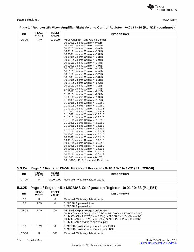
Page 1 Registers www.ti.com
Page 1 / Register 25: Mixer Amplifier Right Volume Control Register - 0x01 / 0x19 (P1_R25) (continued)
READ/ RESETBIT DESCRIPTIONWRITE VALUE
D5-D0 R/W 00 0000 Mixer Amplifier Right Volume Control00 0000: Volume Control = 0.0dB00 0001: Volume Control = -0.4dB00 0010: Volume Control = -0.9dB00 0011: Volume Control = -1.3dB00 0100: Volume Control = -1.8dB00 0101: Volume Control = -2.3dB00 0110: Volume Control = -2.9dB00 0111: Volume Control = -3.3dB00 1000: Volume Control = -3.9dB00 1001: Volume Control = -4.3dB00 1010: Volume Control = -4.8dB00 1011: Volume Control = -5.2dB00 1100: Volume Control = -5.8dB00 1101: Volume Control = -6.3dB00 1110: Volume Control = -6.6dB00 1111: Volume Control = -7.2dB01 0000: Volume Control = -7.8dB01 0001: Volume Control = -8.2dB01 0010: Volume Control = -8.5dB01 0011: Volume Control = -9.3dB01 0100: Volume Control = -9.7dB01 0101: Volume Control = -10.1dB01 0110: Volume Control = -10.6dB01 0111: Volume Control = -11.0dB01 1000: Volume Control = -11.5dB01 1001: Volume Control = -12.0dB01 1010: Volume Control = -12.6dB01 1011: Volume Control = -13.2dB01 1100: Volume Control = -13.8dB01 1101: Volume Control = -14.5dB01 1110: Volume Control = -15.3dB01 1111: Volume Control = -16.1dB10 0000: Volume Control = -17.0dB10 0001: Volume Control = -18.1dB10 0010: Volume Control = -19.2dB10 0011: Volume Control = -20.6dB10 0100: Volume Control = -22.1dB10 0101: Volume Control = -24.1dB10 0110: Volume Control = -26.6dB10 0111: Volume Control = -30.1dB10 1000: Volume Control = MUTE10 1001-11 1111: Reserved. Do no use
5.3.24 Page 1 / Register 26-50: Reserved Register - 0x01 / 0x1A-0x32 (P1_R26-50)READ/ RESETBIT DESCRIPTIONWRITE VALUE
D7-D0 R 0000 0000 Reserved. Write only default values
5.3.25 Page 1 / Register 51: MICBIAS Configuration Register - 0x01 / 0x33 (P1_R51)READ/ RESETBIT DESCRIPTIONWRITE VALUE
D7 R 0 Reserved. Write only default value.
D6 R/W 0 0: MICBIAS powered down1: MICBIAS powered up
D5-D4 R/W 00 MICBIAS Output Voltage Configuration00: MICBIAS = 1.04V (CM = 0.75V) or MICBIAS = 1.25V(CM = 0.9V)01: MICBIAS = 1.425V(CM = 0.75V) or MICBIAS = 1.7V(CM = 0.9V)10: MICBIAS = 2.075V(CM = 0.75V) or MICBIAS = 2.5V(CM = 0.9V)11: MICBIAS is switch to power supply
D3 R/W 0 0: MICBIAS voltage is generated from AVDD1: MICBIAS voltage is generated from LDOIN
D2-D0 R 000 Reserved. Write only default value.
134 Register Map SLAA557–November 2012Submit Documentation Feedback
Copyright © 2012, Texas Instruments Incorporated

www.ti.com Page 1 Registers
5.3.26 Page 1 / Register 52: Left MICPGA Positive Terminal Input Routing ConfigurationRegister - 0x01 / 0x34 (P1_R52)
READ/ RESETBIT DESCRIPTIONWRITE VALUE
D7-D6 R/W 00 IN1L to Left MICPGA positive terminal selection00: IN1L is not routed to Left MICPGA01: IN1L is routed to Left MICPGA with 10k resistance10: IN1L is routed to Left MICPGA with 20k resistance11: IN1L is routed to Left MICPGA with 40k resistance
D5-D4 R/W 00 IN2L to Left MICPGA positive terminal selection00: IN2L is not routed to Left MICPGA01: IN2L is routed to Left MICPGA with 10k resistance10: IN2L is routed to Left MICPGA with 20k resistance11: IN2L is routed to Left MICPGA with 40k resistance
D3-D2 R/W 00 IN3L to Left MICPGA positive terminal selection00: IN3L is not routed to Left MICPGA01: IN3L is routed to Left MICPGA with 10k resistance10: IN3L is routed to Left MICPGA with 20k resistance11: IN3L is routed to Left MICPGA with 40k resistance
D1-D0 R/W 00 IN1R to Left MICPGA positive terminal selection00: IN1R is not routed to Left MICPGA01: IN1R is routed to Left MICPGA with 10k resistance10: IN1R is routed to Left MICPGA with 20k resistance11: IN1R is routed to Left MICPGA with 40k resistance
5.3.27 Page 1 / Register 53: Reserved Register - 0x01 / 0x35 (P1_R53)READ/ RESETBIT DESCRIPTIONWRITE VALUE
D7-D0 R 0000 0000 Reserved. Write only default values
5.3.28 Page 1 / Register 54: Left MICPGA Negative Terminal Input Routing ConfigurationRegister - 0x01 / 0x36 (P1_R54)
READ/ RESETBIT DESCRIPTIONWRITE VALUE
D7-D6 R/W 00 CM to Left MICPGA (CM1L) positive terminal selection00: CM is not routed to Left MICPGA01: CM is routed to Left MICPGA via CM1L with 10k resistance10: CM is routed to Left MICPGA via CM1L with 20k resistance11: CM is routed to Left MICPGA via CM1L with 40k resistance
D5-D4 R/W 00 IN2R to Left MICPGA positive terminal selection00: IN2R is not routed to Left MICPGA01: IN2R is routed to Left MICPGA with 10k resistance10: IN2R is routed to Left MICPGA with 20k resistance11: IN2R is routed to Left MICPGA with 40k resistance
D3-D2 R/W 00 IN3R to Left MICPGA positive terminal selection00: IN3R is not routed to Left MICPGA01: IN3R is routed to Left MICPGA with 10k resistance10: IN3R is routed to Left MICPGA with 20k resistance11: IN3R is routed to Left MICPGA with 40k resistance
D1-D0 R/W 00 CM to Left MICPGA (CM2L) positive terminal selection00: CM is not routed to Left MICPGA01: CM is routed to Left MICPGA via CM2L with 10k resistance10: CM is routed to Left MICPGA via CM2L with 20k resistance11: CM is routed to Left MICPGA via CM2L with 40k resistance
5.3.29 Page 1 / Register 55: Right MICPGA Positive Terminal Input Routing Configuration
135SLAA557–November 2012 Register MapSubmit Documentation Feedback
Copyright © 2012, Texas Instruments Incorporated

Page 1 Registers www.ti.com
Register - 0x01 / 0x37 (P1_R55)READ/ RESETBIT DESCRIPTIONWRITE VALUE
D7-D6 R/W 00 IN1R to Right MICPGA positive terminal selection00: IN1R is not routed to Right MICPGA01: IN1R is routed to Right MICPGA with 10k resistance10: IN1R is routed to Right MICPGA with 20k resistance11: IN1R is routed to Right MICPGA with 40k resistance
D5-D4 R/W 00 IN2R to Right MICPGA positive terminal selection00: IN2R is not routed to Right MICPGA01: IN2R is routed to Right MICPGA with 10k resistance10: IN2R is routed to Right MICPGA with 20k resistance11: IN2R is routed to Right MICPGA with 40k resistance
D3-D2 R/W 00 IN3R to Right MICPGA positive terminal selection00: IN3R is not routed to Right MICPGA01: IN3R is routed to Right MICPGA with 10k resistance10: IN3R is routed to Right MICPGA with 20k resistance11: IN3R is routed to Right MICPGA with 40k resistance
D1-D0 R/W 00 IN2L to Right MICPGA positive terminal selection00: IN2L is not routed to Right MICPGA01: IN2L is routed to Right MICPGA with 10k resistance10: IN2L is routed to Right MICPGA with 20k resistance11: IN2L is routed to Right MICPGA with 40k resistance
5.3.30 Page 1 / Register 56: Reserved Register - 0x01 / 0x38 (P1_R56)READ/ RESETBIT DESCRIPTIONWRITE VALUE
D7-D0 R 0000 0000 Reserved. Write only default values
5.3.31 Page 1 / Register 57: Right MICPGA Negative Terminal Input Routing ConfigurationRegister - 0x01 / 0x39 (P1_R57)
READ/ RESETBIT DESCRIPTIONWRITE VALUE
D7-D6 R/W 00 CM to Right MICPGA (CM1R) positive terminal selection00: CM is not routed to Right MICPGA01: CM is routed to Right MICPGA via CM1R with 10k resistance10: CM is routed to Right MICPGA via CM1R with 20k resistance11: CM is routed to Right MICPGA via CM1R with 40k resistance
D5-D4 R/W 00 IN1L to Right MICPGA positive terminal selection00: IN1L is not routed to Right MICPGA01: IN1L is routed to Right MICPGA with 10k resistance10: IN1L is routed to Right MICPGA with 20k resistance11: IN1L is routed to Right MICPGA with 40k resistance
D3-D2 R/W 00 IN3L to Right MICPGA positive terminal selection00: IN3L is not routed to Right MICPGA01: IN3L is routed to Right MICPGA with 10k resistance10: IN3L is routed to Right MICPGA with 20k resistance11: IN3L is routed to Right MICPGA with 40k resistance
D1-D0 R/W 00 CM to Right MICPGA (CM2R) positive terminal selection00: CM is not routed to Right MICPGA01: CM is routed to Right MICPGA via CM2R with 10k resistance10: CM is routed to Right MICPGA via CM2R with 20k resistance11: CM is routed to Right MICPGA via CM2R with 40k resistance
5.3.32 Page 1 / Register 58: Floating Input Configuration Register - 0x01 / 0x3A (P1_R58)READ/ RESETBIT DESCRIPTIONWRITE VALUE
D7 R/W 0 0: IN1L input is not weakly connected to common mode1: IN1L input is weakly driven to common mode. Use when not routing IN1L to Left and RightMICPGA and HPL
D6 R/W 0 0: IN1R input is not weakly connected to common mode1: IN1R input is weakly driven to common mode. Use when not routing IN1L to Left and RightMICPGA and HPR
136 Register Map SLAA557–November 2012Submit Documentation Feedback
Copyright © 2012, Texas Instruments Incorporated

www.ti.com Page 1 Registers
Page 1 / Register 58: Floating Input Configuration Register - 0x01 / 0x3A (P1_R58) (continued)
READ/ RESETBIT DESCRIPTIONWRITE VALUE
D5 R/W 0 0: IN2L input is not weakly connected to common mode1: IN2L input is weakly driven to common mode. Use when not routing IN2L to Left and RightMICPGA
D4 R/W 0 0: IN2R input is not weakly connected to common mode1: IN2R input is weakly driven to common mode. Use when not routing IN2R to Left and RightMICPGA
D3 R/W 0 0: IN3L input is not weakly connected to common mode1: IN3L input is weakly driven to common mode. Use when not routing IN3L to Left and RightMICPGA
D2 R/W 0 0: IN3R input is not weakly connected to common mode1: IN3R input is weakly driven to common mode. Use when not routing IN3R to Left and RightMICPGA
D1-D0 R 00 Reserved. Write only default values
5.3.33 Page 1 / Register 59: Left MICPGA Volume Control Register - 0x01 / 0x3B (P1_R59)READ/ RESETBIT DESCRIPTIONWRITE VALUE
D7 R/W 1 0: Left MICPGA Gain is enabled1: Left MICPGA Gain is set to 0dB
D6-D0 R/W 000 0000 Left MICPGA Volume Control000 0000: Volume Control = 0.0dB000 0001: Volume Control = 0.5dB000 0010: Volume Control = 1.0dB…101 1101: Volume Control = 46.5dB101 1110: Volume Control = 47.0dB101 1111: Volume Control = 47.5dB110 0000-111 1111: Reserved. Do not use
5.3.34 Page 1 / Register 60: Right MICPGA Volume Control Register - 0x01 / 0x3C (P1_R60)READ/ RESETBIT DESCRIPTIONWRITE VALUE
D7 R/W 1 0: Right MICPGA Gain is enabled1: Right MICPGA Gain is set to 0dB
D6-D0 R/W 000 0000 Right MICPGA Volume Control000 0000: Volume Control = 0.0dB000 0001: Volume Control = 0.5dB000 0010: Volume Control = 1.0dB…101 1101: Volume Control = 46.5dB101 1110: Volume Control = 47.0dB101 1111: Volume Control = 47.5dB110 0000-111 1111: Reserved. Do not use
5.3.35 Page 1 / Register 61: ADC Power Tune Configuration Register - 0x01 / 0x3D (P1_R61)READ/ RESETBIT DESCRIPTIONWRITE VALUE
D7-D0 R/W 0000 0000 0000 0000: PTM_R4 (Default)0110 0100: PTM_R31011 0110: PTM_R21111 1111: PTM_R1
5.3.36 Page 1 / Register 62: ADC Analog Volume Control Flag Register - 0x01 / 0x3E (P1_R62)READ/ RESETBIT DESCRIPTIONWRITE VALUE
D7-D2 R 00 0000 Reserved. Write only default values
137SLAA557–November 2012 Register MapSubmit Documentation Feedback
Copyright © 2012, Texas Instruments Incorporated

Page 1 Registers www.ti.com
Page 1 / Register 62: ADC Analog Volume Control Flag Register - 0x01 / 0x3E (P1_R62) (continued)
READ/ RESETBIT DESCRIPTIONWRITE VALUE
D1 R 0 Left Channel Analog Volume Control Flag0: Applied Volume is not equal to Programmed Volume1: Applied Volume is equal to Programmed Volume
D0 R 0 Right Channel Analog Volume Control Flag0: Applied Volume is not equal to Programmed Volume1: Applied Volume is equal to Programmed Volume
5.3.37 Page 1 / Register 63: DAC Analog Gain Control Flag Register - 0x01 / 0x3F (P1_R63)READ/ RESETBIT DESCRIPTIONWRITE VALUE
D7 R 0 HPL Gain Flag0: Applied Gain is not equal to Programmed Gain1: Applied Gain is equal to Programmed Gain
D6 R 0 HPR Gain Flag0: Applied Gain is not equal to Programmed Gain1: Applied Gain is equal to Programmed Gain
D5 R 0 LOL Gain Flag0: Applied Gain is not equal to Programmed Gain1: Applied Gain is equal to Programmed Gain
D4 R 0 LOR Gain Flag0: Applied Gain is not equal to Programmed Gain1: Applied Gain is equal to Programmed Gain
D3 R 0 IN1L to HPL Bypass Volume Flag0: Applied Volume is not equal to Programmed Volume1: Applied Volume is equal to Programmed Volume
D2 R 0 IN1R to HPR Bypass Volume Flag0: Applied Volume is not equal to Programmed Volume1: Applied Volume is equal to Programmed Volume
D1 R 0 MAL Volume Flag0: Applied Volume is not equal to Programmed Volume1: Applied Volume is equal to Programmed Volume
D0 R 0 MAR Volume Flag0: Applied Volume is not equal to Programmed Volume1: Applied Volume is equal to Programmed Volume
5.3.38 Page 1 / Register 64-70: Reserved Register - 0x01 / 0x40-0x46 (P1_R64-70)READ/ RESETBIT DESCRIPTIONWRITE VALUE
D7-D0 R 0000 0000 Reserved. Write only default values
5.3.39 Page 1 / Register 71: Analog Input Quick Charging Configuration Register - 0x01 / 0x47(P1_R71)
READ/ RESETBIT DESCRIPTIONWRITE VALUE
D7-D6 R 00 Reserved. Write only default values
D5-D0 R/W 00 0000 Analog inputs power up time00 0000: Default. Use one of the values give below11 0001: Analog inputs power up time is 3.1 ms11 0010: Analog inputs power up time is 6.4 ms11 0011: Analog inputs power up time is 1.6 msOthers: Do not use
5.3.40 Page 1 / Register 72-122: Reserved Register - 0x01 / 0x48-0x7A (P1_R72-122)READ/ RESETBIT DESCRIPTIONWRITE VALUE
D7-D0 R 0000 0000 Reserved. Write only default values
138 Register Map SLAA557–November 2012Submit Documentation Feedback
Copyright © 2012, Texas Instruments Incorporated

www.ti.com Page 8 Registers
5.3.41 Page 1 / Register 123: Reference Power-up Configuration Register - 0x01 / 0x7B(P1_R123)
READ/ RESETBIT DESCRIPTIONWRITE VALUE
D7-D3 R 0 0000 Reserved. Write only default values
D2-D0 R/W 000 Reference Power Up configuration000: Reference will power up slowly when analog blocks are powered up001: Reference will power up in 40ms when analog blocks are powered up010: Reference will power up in 80ms when analog blocks are powered up011: Reference will power up in 120ms when analog blocks are powered up100: Force power up of reference. Power up will be slow101: Force power up of reference. Power up time will be 40ms110: Force power up of reference. Power up time will be 80ms111: Force power up of reference. Power up time will be 120ms
5.3.42 Page 1 / Register 124-127: Reserved Register - 0x01 / 0x7C-0x7F (P1_R124-127)READ/ RESETBIT DESCRIPTIONWRITE VALUE
D7-D0 R 0000 0000 Reserved. Write only default values
5.4 Page 8 Registers
5.4.1 Page 8 / Register 0: Page Select Register - 0x08 / 0x00 (P8_R0)READ/ RESETBIT DESCRIPTIONWRITE VALUE
D7-D0 R/W 0000 0000 Page Select Register0-255: Selects the Register Page for next read or write command.Refer Table "Summary of Memory Map" for details.
5.4.2 Page 8 / Register 1: ADC Adaptive Filter Configuration Register - 0x08 / 0x01 (P8_R1)READ/ RESETBIT DESCRIPTIONWRITE VALUE
D7-D3 R 0000 0 Reserved. Write only default values
D2 R/W 0 ADC Adaptive Filtering Control0: Adaptive Filtering disabled for ADC1: Adaptive Filtering enabled for ADC
D1 R 0 ADC Adaptive Filter Buffer Control Flag0: In adaptive filter mode, ADC accesses ADC Coefficient Buffer-A and control interface accessesADC Coefficient Buffer-B1: In adaptive filter mode, ADC accesses ADC Coefficient Buffer-B and control interface accessesADC Coefficient Buffer-A
D0 R/W 0 ADC Adaptive Filter Buffer Switch control0: ADC Coefficient Buffers will not be switched at next frame boundary1: ADC Coefficient Buffers will be switched at next frame boundary, if in adaptive filtering mode.This will self clear on switching.
5.4.3 Page 8 / Register 2-7: Reserved - 0x08 / 0x02-0x07 (P8_R2-7)READ/ RESETBIT DESCRIPTIONWRITE VALUE
D7-D0 R 0000 0000 Reserved. Write only default values
5.4.4 Page 8 / Register 8-127: ADC Coefficients Buffer-A C(0:29) - 0x08 / 0x08-0x7F (P8_R8-127)
READ/ RESETBIT DESCRIPTIONWRITE VALUE
D7-D0 R/W xxxx xxxx 24-bit coefficients C0 through C29 of ADC Coefficient Buffer-A. Refer to Table "ADC CoefficientBuffer A Map" for detailsWhen Page-8, Reg-01d, D2='0' (Adaptive filtering disabled) the read write access to these registersis allowed only when ADC channel is powered down
139SLAA557–November 2012 Register MapSubmit Documentation Feedback
Copyright © 2012, Texas Instruments Incorporated
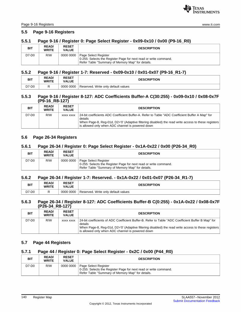
Page 9-16 Registers www.ti.com
5.5 Page 9-16 Registers
5.5.1 Page 9-16 / Register 0: Page Select Register - 0x09-0x10 / 0x00 (P9-16_R0)READ/ RESETBIT DESCRIPTIONWRITE VALUE
D7-D0 R/W 0000 0000 Page Select Register0-255: Selects the Register Page for next read or write command.Refer Table "Summary of Memory Map" for details.
5.5.2 Page 9-16 / Register 1-7: Reserved - 0x09-0x10 / 0x01-0x07 (P9-16_R1-7)READ/ RESETBIT DESCRIPTIONWRITE VALUE
D7-D0 R 0000 0000 Reserved. Write only default values
5.5.3 Page 9-16 / Register 8-127: ADC Coefficients Buffer-A C(30:255) - 0x09-0x10 / 0x08-0x7F(P9-16_R8-127)
READ/ RESETBIT DESCRIPTIONWRITE VALUE
D7-D0 R/W xxxx xxxx 24-bit coefficients ADC Coefficient Buffer-A. Refer to Table "ADC Coefficient Buffer A Map" fordetailsWhen Page-8, Reg-01d, D2='0' (Adaptive filtering disabled) the read write access to these registersis allowed only when ADC channel is powered down
5.6 Page 26-34 Registers
5.6.1 Page 26-34 / Register 0: Page Select Register - 0x1A-0x22 / 0x00 (P26-34_R0)READ/ RESETBIT DESCRIPTIONWRITE VALUE
D7-D0 R/W 0000 0000 Page Select Register0-255: Selects the Register Page for next read or write command.Refer Table "Summary of Memory Map" for details.
5.6.2 Page 26-34 / Register 1-7: Reserved. - 0x1A-0x22 / 0x01-0x07 (P26-34_R1-7)READ/ RESETBIT DESCRIPTIONWRITE VALUE
D7-D0 R 0000 0000 Reserved. Write only default values
5.6.3 Page 26-34 / Register 8-127: ADC Coefficients Buffer-B C(0:255) - 0x1A-0x22 / 0x08-0x7F(P26-34_R8-127)
READ/ RESETBIT DESCRIPTIONWRITE VALUE
D7-D0 R/W xxxx xxxx 24-bit coefficients of ADC Coefficient Buffer-B. Refer to Table "ADC Coefficient Buffer B Map" fordetailsWhen Page-8, Reg-01d, D2='0' (Adaptive filtering disabled) the read write access to these registersis allowed only when ADC channel is powered down
5.7 Page 44 Registers
5.7.1 Page 44 / Register 0: Page Select Register - 0x2C / 0x00 (P44_R0)READ/ RESETBIT DESCRIPTIONWRITE VALUE
D7-D0 R/W 0000 0000 Page Select Register0-255: Selects the Register Page for next read or write command.Refer Table "Summary of Memory Map" for details.
140 Register Map SLAA557–November 2012Submit Documentation Feedback
Copyright © 2012, Texas Instruments Incorporated

www.ti.com Page 45-52 Registers
5.7.2 Page 44 / Register 1: DAC Adaptive Filter Configuration Register - 0x2C / 0x01 (P44_R1)READ/ RESETBIT DESCRIPTIONWRITE VALUE
D7-D3 R 0000 0 Reserved. Write only default values
D2 R/W 0 DAC Adaptive Filtering Control0: Adaptive Filtering disabled for DAC1: Adaptive Filtering enabled for DAC
D1 R 0 DAC Adaptive Filter Buffer Control Flag0: In adaptive filter mode, DAC accesses DAC Coefficient Buffer-A and control interface accessesDAC Coefficient Buffer-B1: In adaptive filter mode, DAC accesses DAC Coefficient Buffer-B and control interface accessesDAC Coefficient Buffer-A
D0 R/W 0 DAC Adaptive Filter Buffer Switch control0: DAC Coefficient Buffers will not be switched at next frame boundary1: DAC Coefficient Buffers will be switched at next frame boundary, if in adaptive filtering mode.This will self clear on switching.
5.7.3 Page 44 / Register 2-7: Reserved - 0x2C / 0x02-0x07 (P44_R2-7)READ/ RESETBIT DESCRIPTIONWRITE VALUE
D7-D0 R 0000 0000 Reserved. Write only default values
5.7.4 Page 44 / Register 8-127: DAC Coefficients Buffer-A C(0:29) - 0x2C / 0x08-0x7F (P44_R8-127)
READ/ RESETBIT DESCRIPTIONWRITE VALUE
D7-D0 R/W xxxx xxxx 24-bit coefficients C0 through C29 of DAC Coefficient Buffer-A. Refer to Table "DAC CoefficientBuffer A Map" for detailsWhen Page-44, Reg-01d, D2='0' (Adaptive filtering disabled) the read write access to theseregisters is allowed only when DAC channel is powered down
5.8 Page 45-52 Registers
5.8.1 Page 45-52 / Register 0: Page Select Register - 0x2D-0x34 / 0x00 (P45-52_R0)READ/ RESETBIT DESCRIPTIONWRITE VALUE
D7-D0 R/W 0000 0000 Page Select Register0-255: Selects the Register Page for next read or write command.Refer Table "Summary of Memory Map" for details.
5.8.2 Page 45-52 / Register 1-7: Reserved. - 0x2D-0x34 / 0x01-0x07 (P45-52_R1-7)READ/ RESETBIT DESCRIPTIONWRITE VALUE
D7-D0 R 0000 0000 Reserved. Write only default values
5.8.3 Page 45-52 / Register 8-127: DAC Coefficients Buffer-A C(30:255) - 0x2D-0x34 / 0x08-0x7F (P45-52_R8-127)
READ/ RESETBIT DESCRIPTIONWRITE VALUE
D7-D0 R/W xxxx xxxx 24-bit coefficients DAC Coefficient Buffer-A. Refer to Table "DAC Coefficient Buffer A Map" fordetailsWhen Page-44, Reg-01d, D2='0' (Adaptive filtering disabled) the read write access to theseregisters is allowed only when DAC channel is powered down
141SLAA557–November 2012 Register MapSubmit Documentation Feedback
Copyright © 2012, Texas Instruments Incorporated

Page 62-70 Registers www.ti.com
5.9 Page 62-70 Registers
5.9.1 Page 62-70 / Register 0: Page Select Register - 0x3E-0x46 / 0x00 (P62-70_R0)READ/ RESETBIT DESCRIPTIONWRITE VALUE
D7-D0 R/W 0000 0000 Page Select Register0-255: Selects the Register Page for next read or write command.Refer Table "Summary of Memory Map" for details.
5.9.2 Page 62-70 / Register 1-7: Reserved. - 0x3E-0x46 / 0x01-0x07 (P62-70_R1-7)READ/ RESETBIT DESCRIPTIONWRITE VALUE
D7-D0 R 0000 0000 Reserved. Write only default values
5.9.3 Page 62-70 / Register 8-127: DAC Coefficients Buffer-B C(0:255) - 0x3E-0x46 / 0x08-0x7F(P62-70_R8-127)
READ/ RESETBIT DESCRIPTIONWRITE VALUE
D7-D0 R/W xxxx xxxx 24-bit coefficients of DAC Coefficient Buffer-B. Refer to Table "DAC Coefficient Buffer B Map" fordetailsWhen Page-44, Reg-01d, D2='0' (Adaptive filtering disabled) the read write access to theseregisters is allowed only when DAC channel is powered down
5.10 ADC Coefficients A+B
Table 5-2. ADC Coefficient Buffer-A Map
Coef No Page Base Register Base Register + 0 Base Register + 1 Base Register + 2 Base Register + 3No
C0 8 8 Coef(23:16) Coef(15:8) Coef(7:0) Reserved.
C1 8 12 Coef(23:16) Coef(15:8) Coef(7:0) Reserved.
.. .. .. .. .. ..
C29 8 124 Coef(23:16) Coef(15:8) Coef(7:0) Reserved.
C30 9 8 Coef(23:16) Coef(15:8) Coef(7:0) Reserved.
.. .. .. .. .. ..
C59 9 124 Coef(23:16) Coef(15:8) Coef(7:0) Reserved.
C60 10 8 Coef(23:16) Coef(15:8) Coef(7:0) Reserved.
.. .. .. .. .. ..
C89 10 124 Coef(23:16) Coef(15:8) Coef(7:0) Reserved.
C90 11 8 Coef(23:16) Coef(15:8) Coef(7:0) Reserved.
.. .. .. .. .. ..
C119 11 124 Coef(23:16) Coef(15:8) Coef(7:0) Reserved.
C120 12 8 Coef(23:16) Coef(15:8) Coef(7:0) Reserved.
.. .. .. .. .. ..
C149 12 124 Coef(23:16) Coef(15:8) Coef(7:0) Reserved.
C150 13 8 Coef(23:16) Coef(15:8) Coef(7:0) Reserved.
.. .. .. .. .. ..
C179 13 124 Coef(23:16) Coef(15:8) Coef(7:0) Reserved.
C180 14 8 Coef(23:16) Coef(15:8) Coef(7:0) Reserved.
.. .. .. .. .. ..
C209 14 124 Coef(23:16) Coef(15:8) Coef(7:0) Reserved.
C210 15 8 Coef(23:16) Coef(15:8) Coef(7:0) Reserved.
.. .. .. .. .. ..
C239 15 124 Coef(23:16) Coef(15:8) Coef(7:0) Reserved.
142 Register Map SLAA557–November 2012Submit Documentation Feedback
Copyright © 2012, Texas Instruments Incorporated

www.ti.com ADC Defaults
Table 5-2. ADC Coefficient Buffer-A Map (continued)
Coef No Page Base Register Base Register + 0 Base Register + 1 Base Register + 2 Base Register + 3No
C240 16 8 Coef(23:16) Coef(15:8) Coef(7:0) Reserved.
.. .. .. .. .. ..
C255 16 68 Coef(23:16) Coef(15:8) Coef(7:0) Reserved.
Table 5-3. ADC Coefficient Buffer-B Map
Coef No Page No Base Base Register + 0 Base Register + 1 Base Register + 2 Base Register + 3Register
C0 26 8 Coef(23:16) Coef(15:8) Coef(7:0) Reserved.
C1 26 12 Coef(23:16) Coef(15:8) Coef(7:0) Reserved.
.. .. .. .. .. ..
C29 26 124 Coef(23:16) Coef(15:8) Coef(7:0) Reserved.
C30 27 8 Coef(23:16) Coef(15:8) Coef(7:0) Reserved.
.. .. .. .. .. ..
C59 27 124 Coef(23:16) Coef(15:8) Coef(7:0) Reserved.
C60 28 8 Coef(23:16) Coef(15:8) Coef(7:0) Reserved.
.. .. .. .. .. ..
C89 28 124 Coef(23:16) Coef(15:8) Coef(7:0) Reserved.
C90 29 8 Coef(23:16) Coef(15:8) Coef(7:0) Reserved.
.. .. .. .. .. ..
C119 29 124 Coef(23:16) Coef(15:8) Coef(7:0) Reserved.
C120 30 8 Coef(23:16) Coef(15:8) Coef(7:0) Reserved.
.. .. .. .. .. ..
C149 30 124 Coef(23:16) Coef(15:8) Coef(7:0) Reserved.
C150 31 8 Coef(23:16) Coef(15:8) Coef(7:0) Reserved.
.. .. .. .. .. ..
C179 31 124 Coef(23:16) Coef(15:8) Coef(7:0) Reserved.
C180 32 8 Coef(23:16) Coef(15:8) Coef(7:0) Reserved.
.. .. .. .. .. ..
C209 32 124 Coef(23:16) Coef(15:8) Coef(7:0) Reserved.
C210 33 8 Coef(23:16) Coef(15:8) Coef(7:0) Reserved.
.. .. .. .. .. ..
C239 33 124 Coef(23:16) Coef(15:8) Coef(7:0) Reserved.
C240 34 8 Coef(23:16) Coef(15:8) Coef(7:0) Reserved.
.. .. .. .. .. ..
C255 34 68 Coef(23:16) Coef(15:8) Coef(7:0) Reserved.
5.11 ADC Defaults
Table 5-4. Default values of ADC Coefficients inBuffers A and B
ADC Buffer-A,B Default Value at reset
Coefficients
C0 00000000H
C1 01170000H
C2 01170000H
143SLAA557–November 2012 Register MapSubmit Documentation Feedback
Copyright © 2012, Texas Instruments Incorporated

DAC Coefficients A+B www.ti.com
Table 5-4. Default values of ADC Coefficients inBuffers A and B (continued)
ADC Buffer-A,B Default Value at reset
Coefficients
C3 7DD30000H
C4 7FFFFF00H
C5,C6 00000000H
C7 7FFFFF00H
C8,..,C11 00000000H
C12 7FFFFF00H
C13,..,C16 00000000H
C17 7FFFFF00H
C18,..,C21 00000000H
C22 7FFFFF00H
C23,..,C26 00000000H
C27 7FFFFF00H
C28,..,C35 00000000H
C36 7FFFFF00H
C37,C38 00000000H
C39 7FFFFF00H
C40,..,C43 00000000H
C44 7FFFFF00H
C45,..,C48 00000000H
C49 7FFFFF00H
C50,..,C53 00000000H
C54 7FFFFF00H
C55,..,C58 00000000H
C59 7FFFFF00H
C60,..,C255 00000000H
5.12 DAC Coefficients A+B
Table 5-5. DAC Coefficient Buffer-A Map
Coef No Page No Base Register Base Register + 0 Base Register + 1 Base Register + 2 Base Register + 3
C0 44 8 Coef(23:16) Coef(15:8) Coef(7:0) Reserved.
C1 44 12 Coef(23:16) Coef(15:8) Coef(7:0) Reserved.
.. .. .. .. .. ..
C29 44 124 Coef(23:16) Coef(15:8) Coef(7:0) Reserved.
C30 45 8 Coef(23:16) Coef(15:8) Coef(7:0) Reserved.
.. .. .. .. .. ..
C59 45 124 Coef(23:16) Coef(15:8) Coef(7:0) Reserved.
C60 46 8 Coef(23:16) Coef(15:8) Coef(7:0) Reserved.
.. .. .. .. .. ..
C89 46 124 Coef(23:16) Coef(15:8) Coef(7:0) Reserved.
C90 47 8 Coef(23:16) Coef(15:8) Coef(7:0) Reserved.
.. .. .. .. .. ..
C119 47 124 Coef(23:16) Coef(15:8) Coef(7:0) Reserved.
C120 48 8 Coef(23:16) Coef(15:8) Coef(7:0) Reserved.
144 Register Map SLAA557–November 2012Submit Documentation Feedback
Copyright © 2012, Texas Instruments Incorporated

www.ti.com DAC Coefficients A+B
Table 5-5. DAC Coefficient Buffer-A Map (continued)
Coef No Page No Base Register Base Register + 0 Base Register + 1 Base Register + 2 Base Register + 3
.. .. .. .. .. ..
C149 48 124 Coef(23:16) Coef(15:8) Coef(7:0) Reserved.
C150 49 8 Coef(23:16) Coef(15:8) Coef(7:0) Reserved.
.. .. .. .. .. ..
C179 49 124 Coef(23:16) Coef(15:8) Coef(7:0) Reserved.
C180 50 8 Coef(23:16) Coef(15:8) Coef(7:0) Reserved.
.. .. .. .. .. ..
C209 50 124 Coef(23:16) Coef(15:8) Coef(7:0) Reserved.
C210 51 8 Coef(23:16) Coef(15:8) Coef(7:0) Reserved.
.. .. .. .. .. ..
C239 51 124 Coef(23:16) Coef(15:8) Coef(7:0) Reserved.
C240 52 8 Coef(23:16) Coef(15:8) Coef(7:0) Reserved.
.. .. .. .. .. ..
C255 52 68 Coef(23:16) Coef(15:8) Coef(7:0) Reserved.
Table 5-6. DAC Coefficient Buffer-B Map
Coef No Page No Base Register Base Register + 0 Base Register + 1 Base Register + 2 Base Register + 3
C0 62 8 Coef(23:16) Coef(15:8) Coef(7:0) Reserved.
C1 62 12 Coef(23:16) Coef(15:8) Coef(7:0) Reserved.
.. .. .. .. .. ..
C29 62 124 Coef(23:16) Coef(15:8) Coef(7:0) Reserved.
C30 63 8 Coef(23:16) Coef(15:8) Coef(7:0) Reserved.
.. .. .. .. .. ..
C59 63 124 Coef(23:16) Coef(15:8) Coef(7:0) Reserved.
C60 64 8 Coef(23:16) Coef(15:8) Coef(7:0) Reserved.
.. .. .. .. .. ..
C89 64 124 Coef(23:16) Coef(15:8) Coef(7:0) Reserved.
C90 65 8 Coef(23:16) Coef(15:8) Coef(7:0) Reserved.
.. .. .. .. .. ..
C119 65 124 Coef(23:16) Coef(15:8) Coef(7:0) Reserved.
C120 66 8 Coef(23:16) Coef(15:8) Coef(7:0) Reserved.
.. .. .. .. .. ..
C149 66 124 Coef(23:16) Coef(15:8) Coef(7:0) Reserved.
C150 67 8 Coef(23:16) Coef(15:8) Coef(7:0) Reserved.
.. .. .. .. .. ..
C179 67 124 Coef(23:16) Coef(15:8) Coef(7:0) Reserved.
C180 68 8 Coef(23:16) Coef(15:8) Coef(7:0) Reserved.
.. .. .. .. .. ..
C209 68 124 Coef(23:16) Coef(15:8) Coef(7:0) Reserved.
C210 69 8 Coef(23:16) Coef(15:8) Coef(7:0) Reserved.
.. .. .. .. .. ..
C239 69 124 Coef(23:16) Coef(15:8) Coef(7:0) Reserved.
C240 70 8 Coef(23:16) Coef(15:8) Coef(7:0) Reserved.
.. .. .. .. .. ..
C255 70 68 Coef(23:16) Coef(15:8) Coef(7:0) Reserved.
145SLAA557–November 2012 Register MapSubmit Documentation Feedback
Copyright © 2012, Texas Instruments Incorporated

DAC Defaults www.ti.com
5.13 DAC Defaults
Table 5-7. Default values of DAC Coefficients in Buffers A and B
DAC Buffer-A,B Coefficients Default Value at reset
C0 00000000H
C1 7FFFFF00H
C2,..,C5 00000000H
C6 7FFFFF00H
C7,..,C10 00000000H
C11 7FFFFF00H
C12,..,C15 00000000H
C16 7FFFFF00H
C17,..,C20 00000000H
C21 7FFFFF00H
C22,..,C25 00000000H
C26 7FFFFF00H
C27,..,C30 00000000H
C31,C32 00000000H
C33 7FFFFF00H
C34,..,C37 00000000H
C38 7FFFFF00H
C39,..,C42 00000000H
C43 7FFFFF00H
C44,..,C47 00000000H
C48 7FFFFF00H
C49,..,C52 00000000H
C53 7FFFFF00H
C54,..,C57 00000000H
C58 7FFFFF00H
C59,..,C64 00000000H
C65 7FFFFF00H
C66,C67 00000000H
C68 7FFFFF00H
C69,C70 00000000H
C71 7FF70000H
C72 10090000H
C73 7FEF0000H
C74,C75 00110000H
C76 7FDE0000H
C77,..,C255 00000000H
146 Register Map SLAA557–November 2012Submit Documentation Feedback
Copyright © 2012, Texas Instruments Incorporated

IMPORTANT NOTICE
Texas Instruments Incorporated and its subsidiaries (TI) reserve the right to make corrections, enhancements, improvements and otherchanges to its semiconductor products and services per JESD46, latest issue, and to discontinue any product or service per JESD48, latestissue. Buyers should obtain the latest relevant information before placing orders and should verify that such information is current andcomplete. All semiconductor products (also referred to herein as “components”) are sold subject to TI’s terms and conditions of salesupplied at the time of order acknowledgment.
TI warrants performance of its components to the specifications applicable at the time of sale, in accordance with the warranty in TI’s termsand conditions of sale of semiconductor products. Testing and other quality control techniques are used to the extent TI deems necessaryto support this warranty. Except where mandated by applicable law, testing of all parameters of each component is not necessarilyperformed.
TI assumes no liability for applications assistance or the design of Buyers’ products. Buyers are responsible for their products andapplications using TI components. To minimize the risks associated with Buyers’ products and applications, Buyers should provideadequate design and operating safeguards.
TI does not warrant or represent that any license, either express or implied, is granted under any patent right, copyright, mask work right, orother intellectual property right relating to any combination, machine, or process in which TI components or services are used. Informationpublished by TI regarding third-party products or services does not constitute a license to use such products or services or a warranty orendorsement thereof. Use of such information may require a license from a third party under the patents or other intellectual property of thethird party, or a license from TI under the patents or other intellectual property of TI.
Reproduction of significant portions of TI information in TI data books or data sheets is permissible only if reproduction is without alterationand is accompanied by all associated warranties, conditions, limitations, and notices. TI is not responsible or liable for such altereddocumentation. Information of third parties may be subject to additional restrictions.
Resale of TI components or services with statements different from or beyond the parameters stated by TI for that component or servicevoids all express and any implied warranties for the associated TI component or service and is an unfair and deceptive business practice.TI is not responsible or liable for any such statements.
Buyer acknowledges and agrees that it is solely responsible for compliance with all legal, regulatory and safety-related requirementsconcerning its products, and any use of TI components in its applications, notwithstanding any applications-related information or supportthat may be provided by TI. Buyer represents and agrees that it has all the necessary expertise to create and implement safeguards whichanticipate dangerous consequences of failures, monitor failures and their consequences, lessen the likelihood of failures that might causeharm and take appropriate remedial actions. Buyer will fully indemnify TI and its representatives against any damages arising out of the useof any TI components in safety-critical applications.
In some cases, TI components may be promoted specifically to facilitate safety-related applications. With such components, TI’s goal is tohelp enable customers to design and create their own end-product solutions that meet applicable functional safety standards andrequirements. Nonetheless, such components are subject to these terms.
No TI components are authorized for use in FDA Class III (or similar life-critical medical equipment) unless authorized officers of the partieshave executed a special agreement specifically governing such use.
Only those TI components which TI has specifically designated as military grade or “enhanced plastic” are designed and intended for use inmilitary/aerospace applications or environments. Buyer acknowledges and agrees that any military or aerospace use of TI componentswhich have not been so designated is solely at the Buyer's risk, and that Buyer is solely responsible for compliance with all legal andregulatory requirements in connection with such use.
TI has specifically designated certain components which meet ISO/TS16949 requirements, mainly for automotive use. Components whichhave not been so designated are neither designed nor intended for automotive use; and TI will not be responsible for any failure of suchcomponents to meet such requirements.
Products Applications
Audio www.ti.com/audio Automotive and Transportation www.ti.com/automotive
Amplifiers amplifier.ti.com Communications and Telecom www.ti.com/communications
Data Converters dataconverter.ti.com Computers and Peripherals www.ti.com/computers
DLP® Products www.dlp.com Consumer Electronics www.ti.com/consumer-apps
DSP dsp.ti.com Energy and Lighting www.ti.com/energy
Clocks and Timers www.ti.com/clocks Industrial www.ti.com/industrial
Interface interface.ti.com Medical www.ti.com/medical
Logic logic.ti.com Security www.ti.com/security
Power Mgmt power.ti.com Space, Avionics and Defense www.ti.com/space-avionics-defense
Microcontrollers microcontroller.ti.com Video and Imaging www.ti.com/video
RFID www.ti-rfid.com
OMAP Applications Processors www.ti.com/omap TI E2E Community e2e.ti.com
Wireless Connectivity www.ti.com/wirelessconnectivity
Mailing Address: Texas Instruments, Post Office Box 655303, Dallas, Texas 75265Copyright © 2012, Texas Instruments Incorporated


![AT Reference Guide - multitech.com€¦ · CE910 Series AT commands reference guide – commands [...]](https://static.documents.pub/doc/80x56/6062516d02f817666972114f/at-reference-guide-ce910-series-at-commands-reference-guide-a-commands-.jpg)


