1 EXPERIMENT 01 TO INVESTIGATE THE CONSTRUCTION, OPERATION AND CHARACTERISTICS OF SCR Objective 1. Understanding the construction and characteristics of an SCR. 2. Understanding the operation of an SCR. 3. Measure an ACR with ohmmeter. 4. Understanding the gate triggering modes of SCR. Discussion The silicon-controlled rectifier (SCR) is the most important thyristor in the family of PNPN devices. It was developed by General Electric in 1957. The SCR acts as a switch in an AC power control circuit. Fig. 7-1 SCR (a) circuit symbol (b) PNPN structure SCR Operation The SCR is a PNPN four-layer semiconductor device having three terminals: anode (A), cathode (K), and gate (G). The symbol and construction for an SCR are shown in Fig. 7-1. In most control applications, the control signal is applied between the gate and the cathode while the load is connected to either the anode or the cathode in series. The circuit symbol of the SCR is illustrated in Fig. 7-1(a). The direction of arrow refers the direction of anode current. The PNPN four-layer structure for the SCR, shown in Fig. 7-1(b), can be considered as PNP and NPN transistor connected as the manner of Fig. 7-2. We will discuss the operation of an SCR by referring to this equivalent two-transistor circuit. DATE:_______________
Transcript
1
EXPERIMENT 01
TO INVESTIGATE THE CONSTRUCTION, OPERATION AND CHARACTERISTICS OF SCR
Objective
1. Understanding the construction and characteristics of an SCR.2. Understanding the operation of an SCR.3. Measure an ACR with ohmmeter.4. Understanding the gate triggering modes of SCR.
Discussion
The silicon-controlled rectifier (SCR) is the most important thyristor in the family of PNPN devices. It was developed by General Electric in 1957. The SCR acts as a switch in an AC power control circuit.
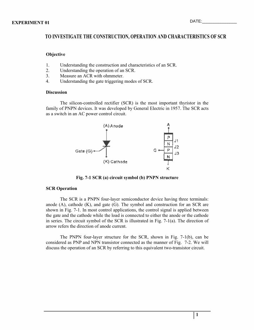
Fig. 7-1 SCR (a) circuit symbol (b) PNPN structure
SCR Operation
The SCR is a PNPN four-layer semiconductor device having three terminals: anode (A), cathode (K), and gate (G). The symbol and construction for an SCR are shown in Fig. 7-1. In most control applications, the control signal is applied between the gate and the cathode while the load is connected to either the anode or the cathode in series. The circuit symbol of the SCR is illustrated in Fig. 7-1(a). The direction of arrow refers the direction of anode current.
The PNPN four-layer structure for the SCR, shown in Fig. 7-1(b), can be considered as PNP and NPN transistor connected as the manner of Fig. 7-2. We will discuss the operation of an SCR by referring to this equivalent two-transistor circuit.
DATE:_______________
2
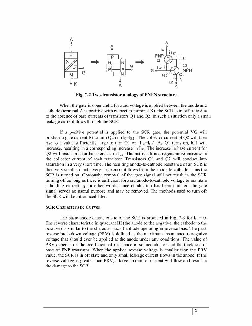
Fig. 7-2 Two-transistor analogy of PNPN structure
When the gate is open and a forward voltage is applied between the anode and cathode (terminal A is positive with respect to terminal K), the SCR is in off state due to the absence of base currents of transistors Q1 and Q2. In such a situation only a small leakage current flows through the SCR.
If a positive potential is applied to the SCR gate, the potential VG will produce a gate current IG to turn Q2 on (IG=IB2). The collector current of Q2 will then rise to a value sufficiently large to turn Q1 on (IB1=IC2). As Q1 turns on, IC1 will increase, resulting in a corresponding increase in IB2. The increase in base current for Q2 will result in a further increase in IC2. The net result is a regenerative increase in the collector current of each transistor. Transistors Q1 and Q2 will conduct into saturation in a very short time. The resulting anode-to-cathode resistance of an SCR is then very small so that a very large current flows from the anode to cathode. Thus the SCR is turned on. Obviously, removal of the gate signal will not result in the SCR turning off as long as there is sufficient forward anode-to-cathode voltage to maintain a holding current IH. In other words, once conduction has been initiated, the gate signal serves no useful purpose and may be removed. The methods used to turn off the SCR will be introduced later.
SCR Characteristic Curves
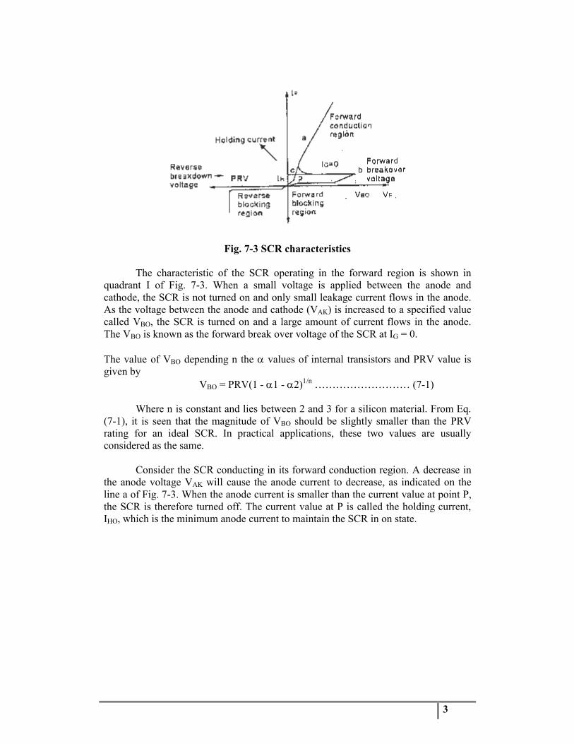
The basic anode characteristic of the SCR is provided in Fig. 7-3 for IG = 0. The reverse characteristic in quadrant III (the anode to the negative, the cathode to the positive) is similar to the characteristic of a diode operating in reverse bias. The peak reverse breakdown voltage (PRV) is defined as the maximum instantaneous negative voltage that should ever be applied at the anode under any conditions. The value of PRV depends on the coefficient of resistance of semiconductor and the thickness of base of PNP transistor. When the applied reverse voltage is smaller than the PRV value, the SCR is in off state and only small leakage current flows in the anode. If the reverse voltage is greater than PRV, a large amount of current will flow and result in the damage to the SCR.
3
Fig. 7-3 SCR characteristics
The characteristic of the SCR operating in the forward region is shown in quadrant I of Fig. 7-3. When a small voltage is applied between the anode and cathode, the SCR is not turned on and only small leakage current flows in the anode. As the voltage between the anode and cathode (VAK) is increased to a specified value called VBO, the SCR is turned on and a large amount of current flows in the anode. The VBO is known as the forward break over voltage of the SCR at IG = 0.
The value of VBO depending n the values of internal transistors and PRV value is given by
VBO = PRV(1 - 1 - 2)1/n ……………………… (7-1)
Where n is constant and lies between 2 and 3 for a silicon material. From Eq. (7-1), it is seen that the magnitude of VBO should be slightly smaller than the PRV rating for an ideal SCR. In practical applications, these two values are usually considered as the same.
Consider the SCR conducting in its forward conduction region. A decrease in the anode voltage VAK will cause the anode current to decrease, as indicated on the line a of Fig. 7-3. When the anode current is smaller than the current value at point P, the SCR is therefore turned off. The current value at P is called the holding current, IHO, which is the minimum anode current to maintain the SCR in on state.
4
Fig. 7-4 SCR output characteristics with variable gate current
The SCR characteristic curve in Fig. 7-3 is plotted with the gate open. If the external signal is applied to the gate, the gate current will change the forward breakover voltage of the SCR. As shown in Fig. 7-4, an increase in IG will cause the VBO to decrease. That is, the greater the IG, the smaller the VBO. In other words, the magnitude of gate current determines the voltage to fire the SCR.
SCR Triggering Characteristics
From the characteristics of the SCR mentioned above, it can be seen that two conditions must be met to fire the SCR. They are:
(1) Anode voltage should be positive with respect to the cathode;(2) Gate voltage should be positive with respect to the cathode.
We have found that successful gate triggering depends on the satisfaction of three conditions:
(1) Trigger current and voltage must be within the triggering area;(2) Power dissipation in gate circuit should be minimized;(3) Trigger signal must be properly timed.
SCR Gate Triggering
Three basic types of gate triggering signals are usually used. These are dc signals, pulse signals and ac shift signals. However, the pulse triggering is the most popular type.
DC Triggering
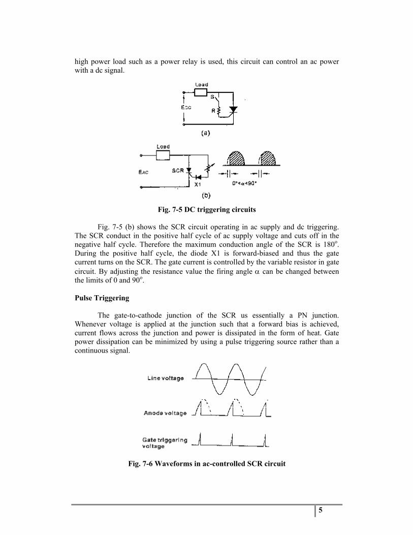
DC triggering signal is rarely used in practical SCR applications. The circuit of Fig. 7-5(a) shows an SCR operating with dc supply and dc triggering signal. When switch S is closed, a sufficient gate current causes the SCR to turn on. The current-limiting resistor R is used to ensure the gate dissipation within its rating. This circuit acts as a dc switch, which uses a low power signal to control a high power load. If a
5
high power load such as a power relay is used, this circuit can control an ac power with a dc signal.
Fig. 7-5 DC triggering circuits
Fig. 7-5 (b) shows the SCR circuit operating in ac supply and dc triggering. The SCR conduct in the positive half cycle of ac supply voltage and cuts off in the negative half cycle. Therefore the maximum conduction angle of the SCR is 180o. During the positive half cycle, the diode X1 is forward-biased and thus the gate current turns on the SCR. The gate current is controlled by the variable resistor in gate circuit. By adjusting the resistance value the firing angle can be changed between the limits of 0 and 90o.
Pulse Triggering
The gate-to-cathode junction of the SCR us essentially a PN junction. Whenever voltage is applied at the junction such that a forward bias is achieved, current flows across the junction and power is dissipated in the form of heat. Gate power dissipation can be minimized by using a pulse triggering source rather than a continuous signal.
Fig. 7-6 Waveforms in ac-controlled SCR circuit
6
Fig. 7-6 shows the relationship of the line voltage, anode voltage and triggering pulses in an ac-controlled SCR circuit. One precaution that must be taken in applying pulse sources at the gate of the SCR is that the reverse bias limit of the gate is not exceeded. A common technique for limiting the negative voltage at the gate is to clamp the gate to the forward drop across a diode.
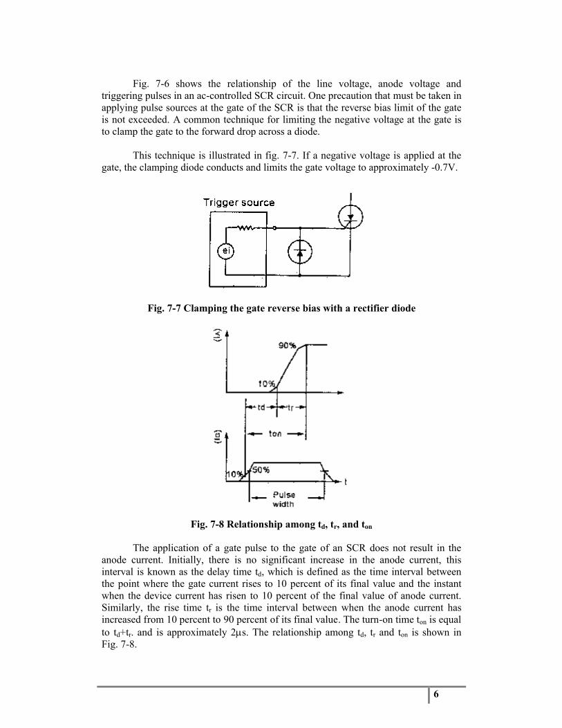
This technique is illustrated in fig. 7-7. If a negative voltage is applied at the gate, the clamping diode conducts and limits the gate voltage to approximately -0.7V.
Fig. 7-7 Clamping the gate reverse bias with a rectifier diode
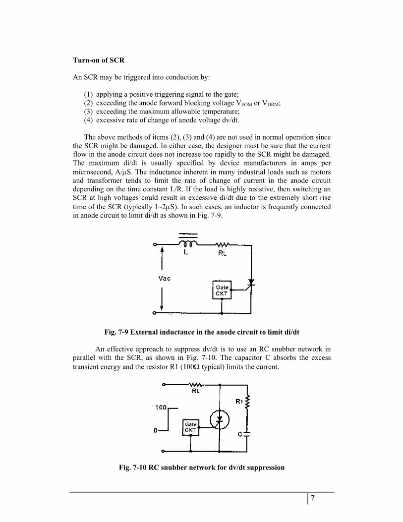
Fig. 7-8 Relationship among td, tr, and ton
The application of a gate pulse to the gate of an SCR does not result in the anode current. Initially, there is no significant increase in the anode current, this interval is known as the delay time td, which is defined as the time interval between the point where the gate current rises to 10 percent of its final value and the instant when the device current has risen to 10 percent of the final value of anode current. Similarly, the rise time tr is the time interval between when the anode current has increased from 10 percent to 90 percent of its final value. The turn-on time ton is equal to td+tr. and is approximately 2s. The relationship among td, tr and ton is shown in Fig. 7-8.
7
Turn-on of SCR
An SCR may be triggered into conduction by:
(1) applying a positive triggering signal to the gate;(2) exceeding the anode forward blocking voltage VFOM or VDRM;(3) exceeding the maximum allowable temperature;(4) excessive rate of change of anode voltage dv/dt.
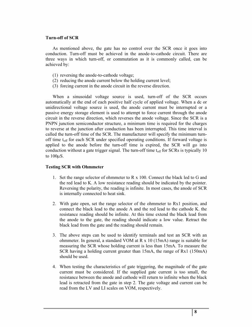
The above methods of items (2), (3) and (4) are not used in normal operation since the SCR might be damaged. In either case, the designer must be sure that the current flow in the anode circuit does not increase too rapidly to the SCR might be damaged. The maximum di/dt is usually specified by device manufacturers in amps per microsecond, A/S. The inductance inherent in many industrial loads such as motors and transformer tends to limit the rate of change of current in the anode circuit depending on the time constant L/R. If the load is highly resistive, then switching an SCR at high voltages could result in excessive di/dt due to the extremely short rise time of the SCR (typically 1~2S). In such cases, an inductor is frequently connected in anode circuit to limit di/dt as shown in Fig. 7-9.
Fig. 7-9 External inductance in the anode circuit to limit di/dt
An effective approach to suppress dv/dt is to use an RC snubber network in parallel with the SCR, as shown in Fig. 7-10. The capacitor C absorbs the excess transient energy and the resistor R1 (100 typical) limits the current.
Fig. 7-10 RC snubber network for dv/dt suppression
8
Turn-off of SCR
As mentioned above, the gate has no control over the SCR once it goes into conduction. Turn-off must be achieved in the anode-to-cathode circuit. There are three ways in which turn-off, or commutation as it is commonly called, can be achieved by:
(1) reversing the anode-to-cathode voltage;(2) reducing the anode current below the holding current level;(3) forcing current in the anode circuit in the reverse direction.
When a sinusoidal voltage source is used, turn-off of the SCR occurs automatically at the end of each positive half cycle of applied voltage. When a dc or unidirectional voltage source is used, the anode current must be interrupted or a passive energy storage element is used to attempt to force current through the anode circuit in the reverse direction, which reverses the anode voltage. Since the SCR is a PNPN junction semiconductor structure, a minimum time is required for the charges to reverse at the junction after conduction has been interrupted. This time interval is called the turn-off time of the SCR. The manufacturer will specify the minimum turn-off time toff for each SCR under specified operating conditions. If forward voltage is applied to the anode before the turn-off time is expired, the SCR will go into conduction without a gate trigger signal. The turn-off time toff for SCRs is typically 10 to 100S.
Testing SCR with Ohmmeter
1. Set the range selector of ohmmeter to R x 100. Connect the black led to G and the red lead to K. A low resistance reading should be indicated by the pointer. Reversing the polarity, the reading is infinite. In most cases, the anode of SCR is internally connected to heat sink.
2. With gate open, set the range selector of the ohmmeter to Rx1 position, and connect the black lead to the anode A and the red lead to the cathode K. the resistance reading should be infinite. At this time extend the black lead from the anode to the gate, the reading should indicate a low value. Retract the black lead from the gate and the reading should remain.
3. The above steps can be used to identify terminals and test an SCR with an ohmmeter. In general, a standard VOM at R x 10 (15mA) range is suitable for measuring the SCR whose holding current is less than 15mA. To measure the SCR having a holding current greater than 15mA, the range of Rx1 (150mA) should be used.
4. When testing the characteristics of gate triggering, the magnitude of the gate current must be considered. If the supplied gate current is too small, the resistance between the anode and cathode will return to infinite when the black lead is retracted from the gate in step 2. The gate voltage and current can be read from the LV and LI scales on VOM, respectively.
9
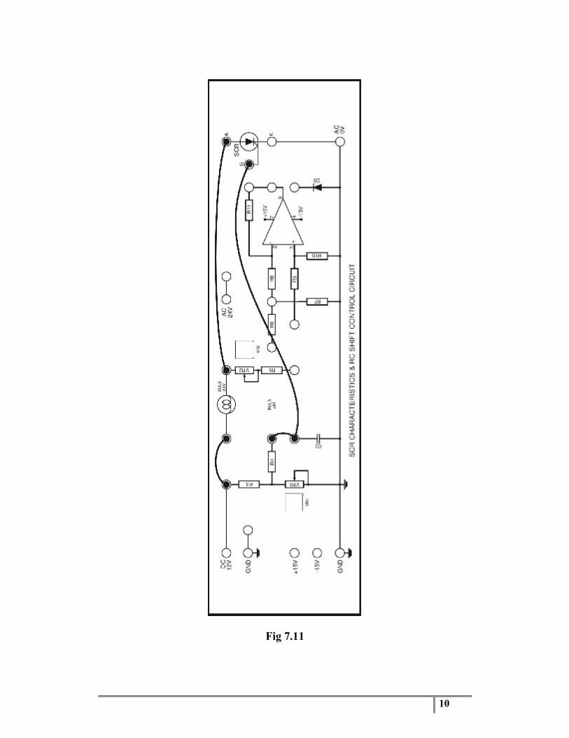
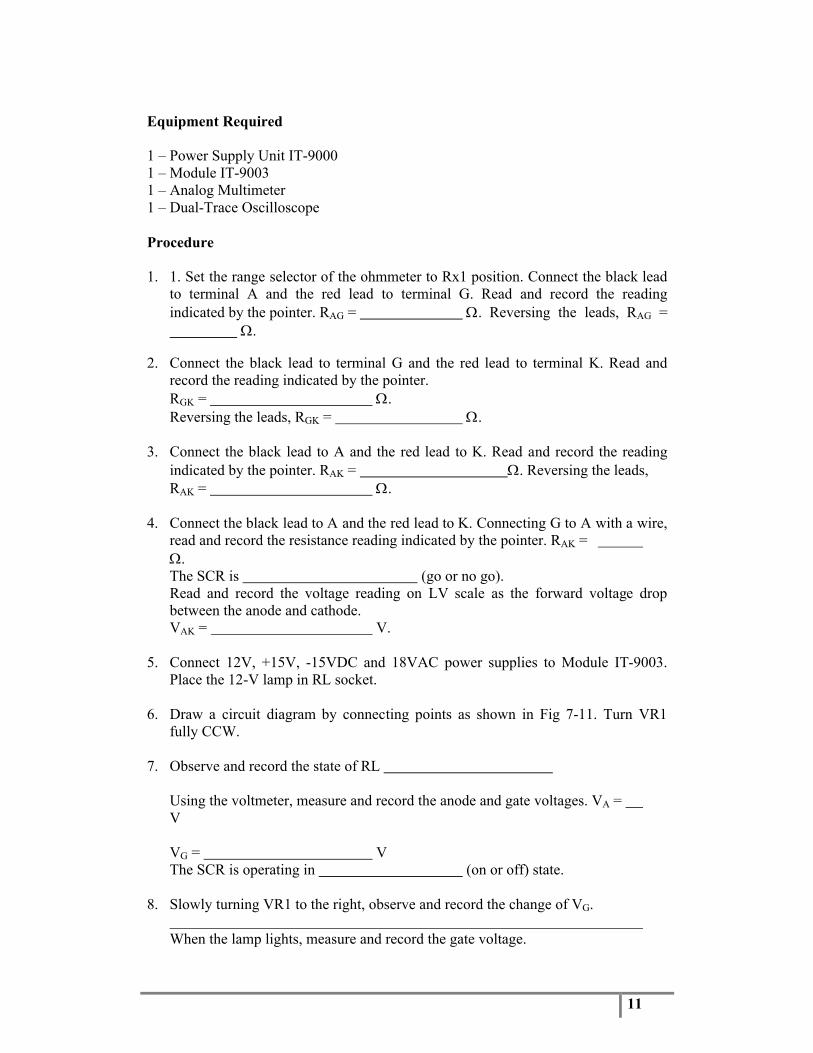
Description of Experiment Circuit
As shown in Fig. 7-11, the experiment circuits contains two major section: dc triggering and ac phase shift triggering. In dc triggering section, when the gate voltage of SCR is 0V (VR1=0), the SCR is off. If the increase in resistance of VR1 rises the gate voltage VG to reach a sufficient level, the SCR will turn on. Once the SCR turns on, the gate voltage is not able to turn off it.
The basic RC network, (VR2+R5) and C3, performs the function of ac phase shifting. As mentioned above, the RC phase shift network varies the firing angles between 0 and 90 degrees. The triggering angle can be calculated by the equation = tan-1RC. To extend the range of firing angles to 180 degrees, the bridge RC network must be used. The OPAMP U1 is used as a differential amplifier to amplify the differential output of bridge network.
10
Fig 7.11
11
Equipment Required
1 – Power Supply Unit IT-90001 – Module IT-90031 – Analog Multimeter1 – Dual-Trace Oscilloscope
Procedure
1. 1. Set the range selector of the ohmmeter to Rx1 position. Connect the black lead to terminal A and the red lead to terminal G. Read and record the reading indicated by the pointer. RAG = . Reversing the leads, RAG =
.
2. Connect the black lead to terminal G and the red lead to terminal K. Read and record the reading indicated by the pointer.RGK = .Reversing the leads, RGK = .
3. Connect the black lead to A and the red lead to K. Read and record the reading indicated by the pointer. RAK = . Reversing the leads, RAK = .
4. Connect the black lead to A and the red lead to K. Connecting G to A with a wire, read and record the resistance reading indicated by the pointer. RAK = . The SCR is (go or no go).Read and record the voltage reading on LV scale as the forward voltage drop between the anode and cathode.VAK = V.
5. Connect 12V, +15V, -15VDC and 18VAC power supplies to Module IT-9003. Place the 12-V lamp in RL socket.
6. Draw a circuit diagram by connecting points as shown in Fig 7-11. Turn VR1 fully CCW.
7. Observe and record the state of RL
Using the voltmeter, measure and record the anode and gate voltages. VA = V
VG = VThe SCR is operating in (on or off) state.
8. Slowly turning VR1 to the right, observe and record the change of VG.
When the lamp lights, measure and record the gate voltage.
12
VG = VThe SCR is operating in (on or off) state.
9. Using the voltmeter, measure and record the anode voltage of the SCR. This voltage is the forward voltage drop (VF) between the anode and cathode of the SCR.
VF = V
10. Turn VR1 fully CW. Observe and record the states RL and SCR.
Turn VR1 fully CCW. Observe and record the states of RL and SCR.
Explain the changes.
11. Remove the connect plug from position 1 and then insert it back. Observe and record the states of RL and SCR.
13
Fig 7.12
14
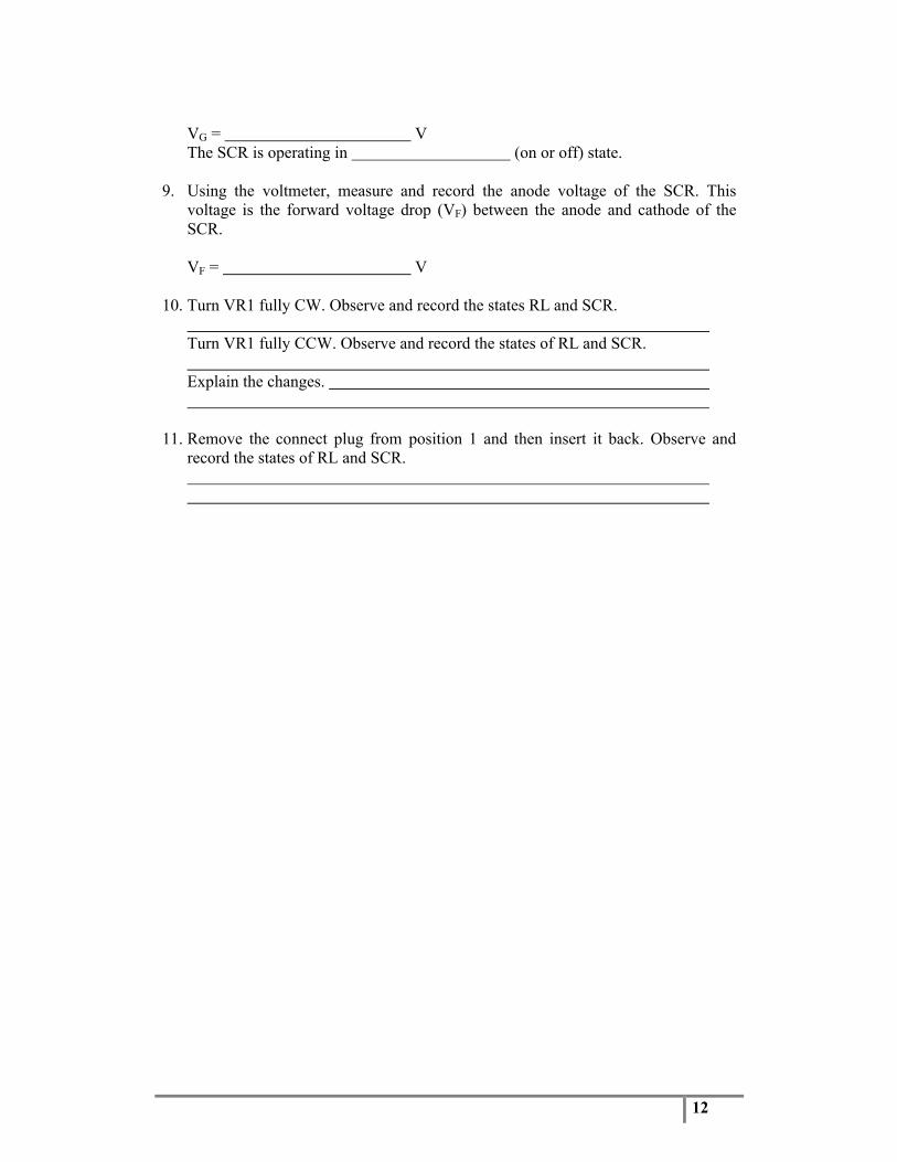
12. Draw Circuit diagram by making connection as in fig 7-12. Using the oscilloscope, measure the voltage waveform across RL.
Turning VR2, observe and record the changes of the SCR conduction angle and lamp brightness.
13. Turn VR2 to get maximum conduction angle.
= degrees.
Using the oscilloscope measure and record the voltage waveforms of VG and UK
in Table 7-1.
Table 7-1
VG VK
15
Fig 7.13
16
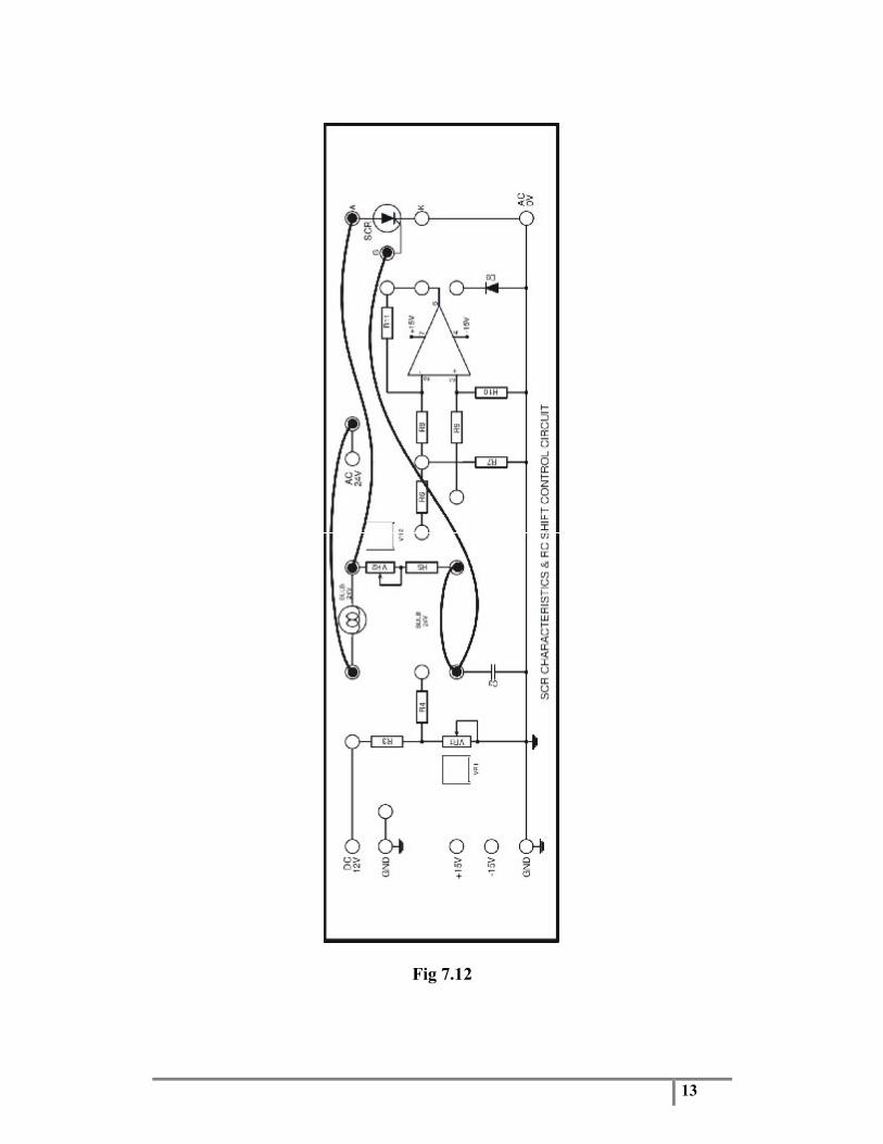
14. Draw a circuit diagram by connecting points as shown in Fig 7-13. Using the oscilloscope, measure the voltage waveform across RL. Turning VR2, observe and record the changes of the SCR conduction angle and lamp brightness.
15. Adjust VR2 to get the conduction angle of 90 degrees. Measure and record the voltage waveforms of VG and VK in Table 7-2.
Table 7-2
VG VK
17
Fig 7.14
18
16. Now remove connection from diode and make connection as in fig 7-14. Observe and record the changes of VG and VK.
Conclusion
You have experimented the dc triggering and ac phase shift triggering for the SCR. When an SCR operates in dc voltage, a dc voltage to the gate will turn on the SCR. The conducting SCR remains in on state even the gate signal is removed. When ac voltage is applied, the SCR is turned on by the gate triggering signal and is automatically turned off when the applied ac voltage reduces to zero voltage on each half cycle.
Signature of Subject Engineer:
20
EXPERIMENT: 04
TO INVESTIGATE THE PHASE CONTROL THROUGH DIAC AND TRIAC
Objective
1. Understanding and measuring the characteristics of TRIAC.2. Understanding and measuring the characteristics of DIAC.3. Performing the DIAC-TRIAC phase control.
DiscussionTRIAC Characteristics
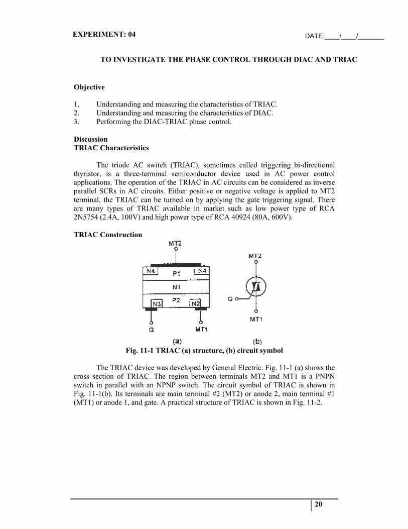
The triode AC switch (TRIAC), sometimes called triggering bi-directional thyristor, is a three-terminal semiconductor device used in AC power control applications. The operation of the TRIAC in AC circuits can be considered as inverse parallel SCRs in AC circuits. Either positive or negative voltage is applied to MT2 terminal, the TRIAC can be turned on by applying the gate triggering signal. There are many types of TRIAC available in market such as low power type of RCA 2N5754 (2.4A, 100V) and high power type of RCA 40924 (80A, 600V).
TRIAC Construction
Fig. 11-1 TRIAC (a) structure, (b) circuit symbol
The TRIAC device was developed by General Electric. Fig. 11-1 (a) shows the cross section of TRIAC. The region between terminals MT2 and MT1 is a PNPN switch in parallel with an NPNP switch. The circuit symbol of TRIAC is shown in Fig. 11-1(b). Its terminals are main terminal #2 (MT2) or anode 2, main terminal #1 (MT1) or anode 1, and gate. A practical structure of TRIAC is shown in Fig. 11-2.
DATE:____/____/_______
21
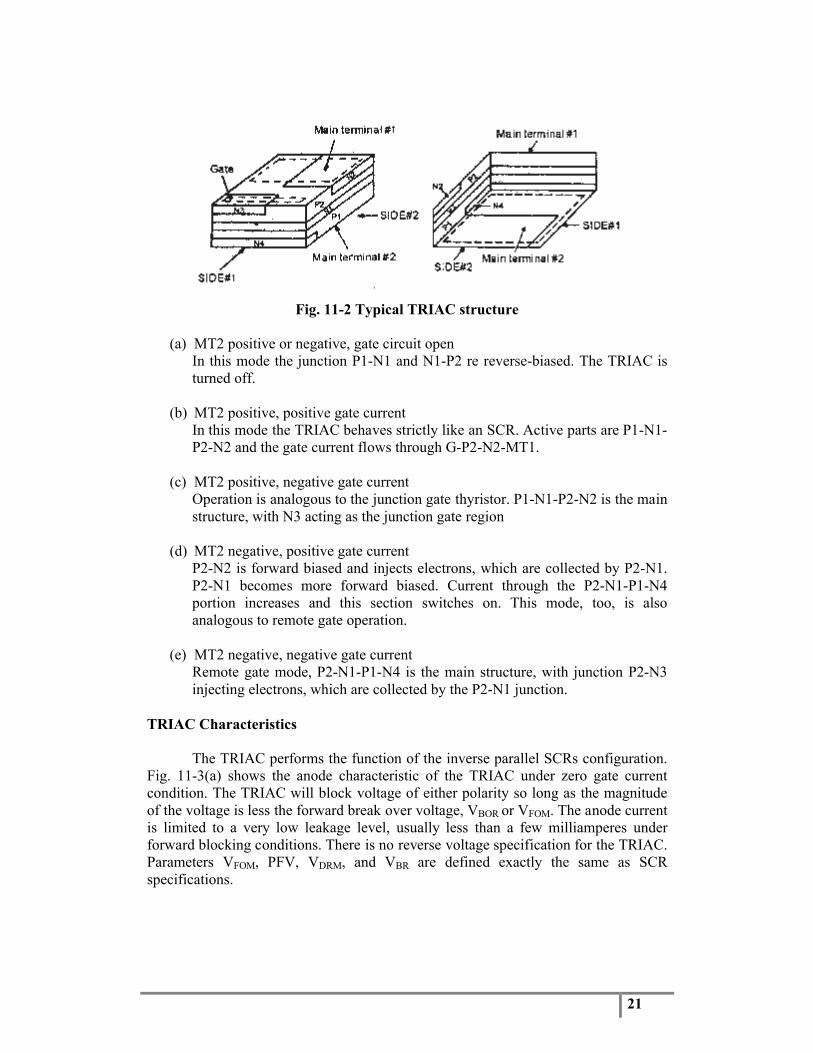
Fig. 11-2 Typical TRIAC structure
(a) MT2 positive or negative, gate circuit openIn this mode the junction P1-N1 and N1-P2 re reverse-biased. The TRIAC is turned off.
(b) MT2 positive, positive gate currentIn this mode the TRIAC behaves strictly like an SCR. Active parts are P1-N1-P2-N2 and the gate current flows through G-P2-N2-MT1.
(c) MT2 positive, negative gate currentOperation is analogous to the junction gate thyristor. P1-N1-P2-N2 is the main structure, with N3 acting as the junction gate region
(d) MT2 negative, positive gate currentP2-N2 is forward biased and injects electrons, which are collected by P2-N1. P2-N1 becomes more forward biased. Current through the P2-N1-P1-N4 portion increases and this section switches on. This mode, too, is also analogous to remote gate operation.
(e) MT2 negative, negative gate currentRemote gate mode, P2-N1-P1-N4 is the main structure, with junction P2-N3 injecting electrons, which are collected by the P2-N1 junction.
TRIAC Characteristics
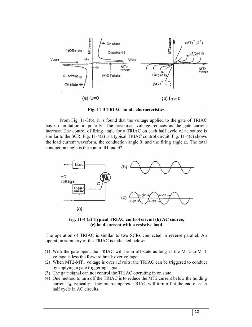
The TRIAC performs the function of the inverse parallel SCRs configuration. Fig. 11-3(a) shows the anode characteristic of the TRIAC under zero gate current condition. The TRIAC will block voltage of either polarity so long as the magnitude of the voltage is less the forward break over voltage, VBOR or VFOM. The anode current is limited to a very low leakage level, usually less than a few milliamperes under forward blocking conditions. There is no reverse voltage specification for the TRIAC. Parameters VFOM, PFV, VDRM, and VBR are defined exactly the same as SCR specifications.
22
Fig. 11-3 TRIAC anode characteristics
From Fig. 11-3(b), it is found that the voltage applied to the gate of TRIAC has no limitation in polarity. The breakover voltage reduces as the gate current increase. The control of firing angle for a TRIAC on each half cycle of ac source is similar to the SCR. Fig. 11-4(a) is a typical TRIAC control circuit. Fig. 11-4(c) shows the load current waveform, the conduction angle , and the firing angle . The total conduction angle is the sum of 1 and 2.
Fig. 11-4 (a) Typical TRIAC control circuit (b) AC source, (c) load current with a resistive load
The operation of TRIAC is similar to two SCRs connected in reverse parallel. An operation summary of the TRIAC is indicated below:
(1) With the gate open, the TRIAC will be in off-state as long as the MT2-to-MT1 voltage is less the forward break over voltage.
(2) When MT2-MT1 voltage is over 1.5volts, the TRIAC can be triggered to conduct by applying a gate triggering signal.
(3) The gate signal can not control the TRIAC operating in on state.(4) One method to turn off the TRIAC is to reduce the MT2 current below the holding
current IH, typically a few microamperes. TRIAC will turn off at the end of each half cycle in AC circuits.
23
(5) The gate signal to turn TRIAC on has no limitation in polarity. The magnitude of triggering current depends upon the polarity of triggering voltage.
(6) The MT2-to-MT1 voltage reduces to a small value of about 1.5V when TRIAC turns on.
Triggering Characteristics of TRIAC
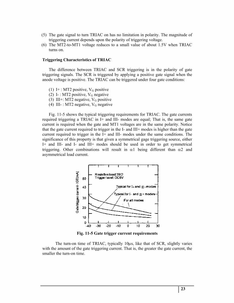
The difference between TRIAC and SCR triggering is in the polarity of gate triggering signals. The SCR is triggered by applying a positive gate signal when the anode voltage is positive. The TRIAC can be triggered under four gate conditions:
Fig. 11-5 shows the typical triggering requirements for TRIAC. The gate currents required triggering a TRIAC in I+ and III- modes are equal; That is, the same gate current is required when the gate and MT1 voltages are in the same polarity. Notice that the gate current required to trigger in the I- and III+ modes is higher than the gate current required to trigger in the I+ and III- modes under the same conditions. The significance of this property is that given a symmetrical gage triggering source, either I+ and III- and I- and III+ modes should be used in order to get symmetrical triggering. Other combinations will result in 1 being different than 2 and asymmetrical load current.
Fig. 11-5 Gate trigger current requirements
The turn-on time of TRIAC, typically 10s, like that of SCR, slightly varies with the amount of the gate triggering current. That is, the greater the gate current, the smaller the turn-on time.
24
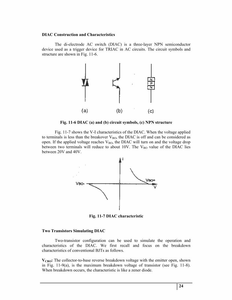
DIAC Construction and Characteristics
The di-electrode AC switch (DIAC) is a three-layer NPN semiconductor device used as a trigger device for TRIAC in AC circuits. The circuit symbols and structure are shown in Fig. 11-6.
Fig. 11-7 shows the V-I characteristics of the DIAC. When the voltage applied to terminals is less than the breakover VBO, the DIAC is off and can be considered as open. If the applied voltage reaches VBO, the DIAC will turn on and the voltage drop between two terminals will reduce to about 10V. The VBO value of the DIAC lies between 20V and 40V.
Fig. 11-7 DIAC characteristic
Two Transistors Simulating DIAC
Two-transistor configuration can be used to simulate the operation and characteristics of the DIAC. We first recall and focus on the breakdown characteristics of conventional BJTs as follows.
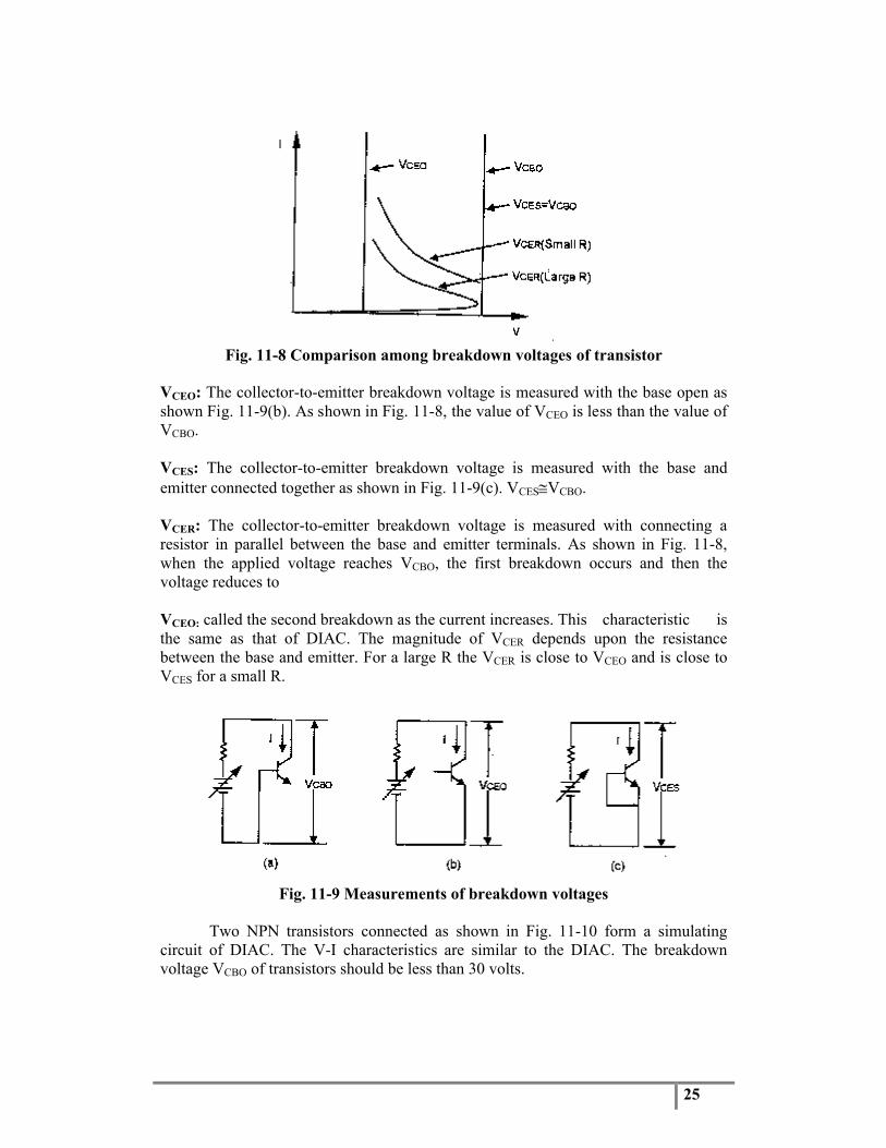
VCBO: The collector-to-base reverse breakdown voltage with the emitter open, shown in Fig. 11-9(a), is the maximum breakdown voltage of transistor (see Fig. 11-8). When breakdown occurs, the characteristic is like a zener diode.
25
Fig. 11-8 Comparison among breakdown voltages of transistor
VCEO: The collector-to-emitter breakdown voltage is measured with the base open as shown Fig. 11-9(b). As shown in Fig. 11-8, the value of VCEO is less than the value of VCBO.
VCES: The collector-to-emitter breakdown voltage is measured with the base and emitter connected together as shown in Fig. 11-9(c). VCESVCBO.
VCER: The collector-to-emitter breakdown voltage is measured with connecting a resistor in parallel between the base and emitter terminals. As shown in Fig. 11-8, when the applied voltage reaches VCBO, the first breakdown occurs and then the voltage reduces to
VCEO: called the second breakdown as the current increases. This characteristic is the same as that of DIAC. The magnitude of VCER depends upon the resistance between the base and emitter. For a large R the VCER is close to VCEO and is close to VCES for a small R.
Fig. 11-9 Measurements of breakdown voltages
Two NPN transistors connected as shown in Fig. 11-10 form a simulating circuit of DIAC. The V-I characteristics are similar to the DIAC. The breakdown voltage VCBO of transistors should be less than 30 volts.
26
Fig. 11-10 Two-transistor configuration to simulate DIAC
DIAC Operation and Testing
The DIAC with negative resistance characteristic can be used in relaxation oscillator circuit. As shown in Fig. 11-11(a), the DIAC acts as neon tube. When the capacitor voltage is less than the breakover voltage of DIAC, the DIAC is off and the capacitor charges through the resistor R. If the capacitor voltage reaches VP, DIAC turns on and the capacitor discharges through DIAC. When the capacitor voltage reduces to Vv, DIAC returns to off and a complete cycle is finished. The voltage waveform is shown in Fig. 11-11(b). Fig. 11-11(c) shows the voltage waveform when the applied voltage is in reversal polarity.
(a) DIAC relaxation oscillator (b) Voltage waveform with +V applied
(C) Voltage waveform with –V appliedFig. 11-11 DIAC relaxation oscillator
27
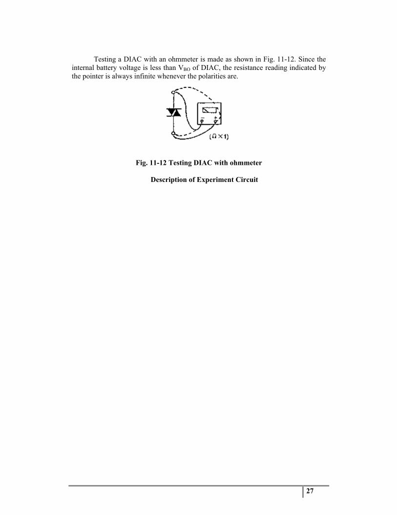
Testing a DIAC with an ohmmeter is made as shown in Fig. 11-12. Since the internal battery voltage is less than VBO of DIAC, the resistance reading indicated by the pointer is always infinite whenever the polarities are.
Fig. 11-12 Testing DIAC with ohmmeter
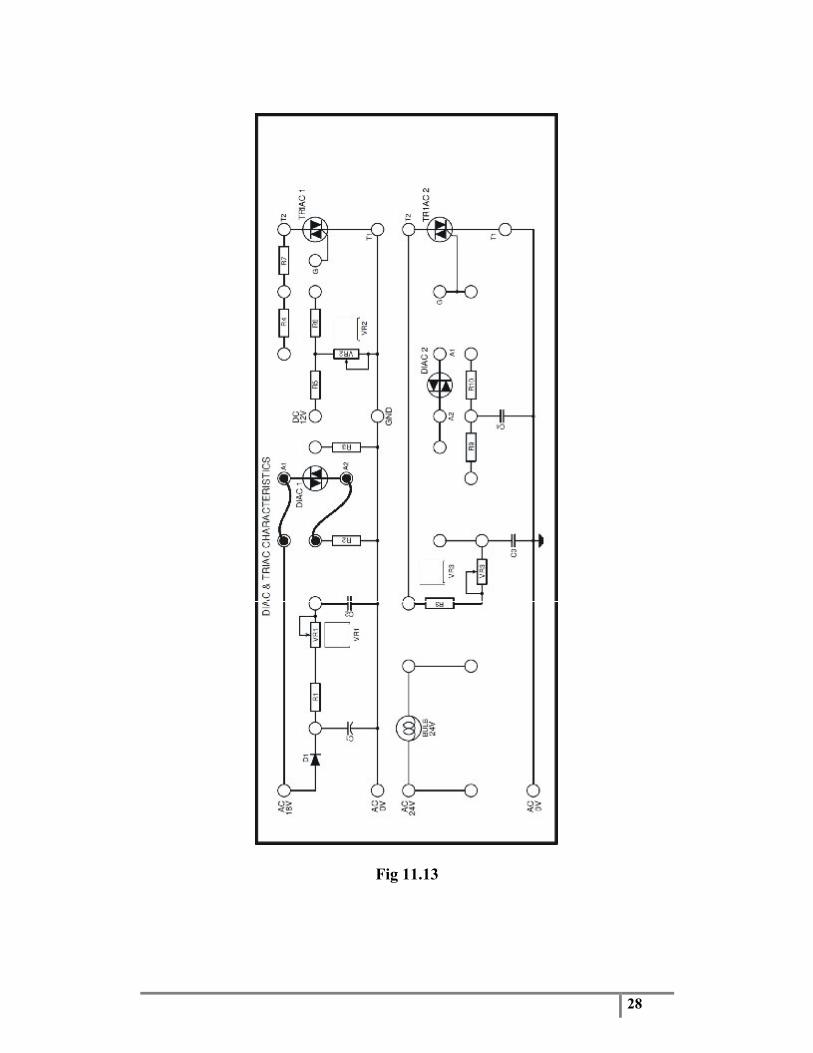
Description of Experiment Circuit
28
Fig 11.13
29
Fig. 11-13 shows the circuits used in the experiment. We will use the upper circuit to perform the characteristic measurements of DIAC and TRIAC. The characteristics of DIAC and TRIAC have been introduced above in detail. The variable resistor VR2 is used to vary the dc voltage to the gate of the TRIAC for plotting the V-I curve. D1 and C1 are used to supply a dc voltage to the DIAC from 36-Vac voltage. VR1 is to control the charging current to capacitor C2.
The lower circuit is a DIAC-TRIAC phase control circuit. As mentioned above, this circuit has a disadvantage of hysteresis phenomenon. R9 and C4 are used to improve the effect.
Equipment Required
1 – Power Supply Unit IT-90001 – Module IT-90031 – Oscilloscope
Procedure
1. Connect 36VAC supplies from Power Supply unit IT-9000 to Module IT-9003. The 36VAC is supplied by connecting two 18VAC supplies in series.
2. Draw a circuit diagram by connecting points as shown in Fig 11-13. Now locate these components on the Module and complete the circuit diagram by connecting the components using the leads with 2mm male pins. Set the oscilloscope to X-Y mode. Connect CH1 input to AC0V terminal, GND to the other terminal of load R2, and CH2 input to AC36V terminal. Adjust scope controls to indicate the V-I characteristic on scope display and plot it in Table 11-1.
3. From the V-I curve, DIAC VBO = volts,. the voltage between two anodes = volts.
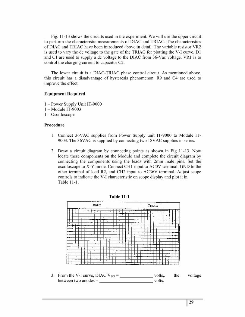
Table 11-1
30
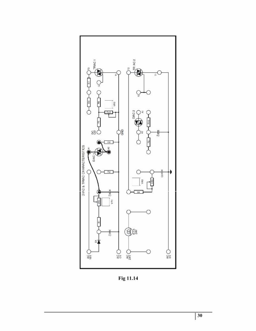
Fig 11.14
31
4. Turn off the power. Make connection as in fig 11-14. Turn on the power. Measure and record the capacitor voltage of C1 using the multimeter.VC1 = V
5. Set VR1 to its midposition. Using the oscilloscope, measure and record the voltage waveform across the capacitor C2 in Table 11-2.
6. From Table 11-2, DIAC VP = volts; VV = Volts.
32
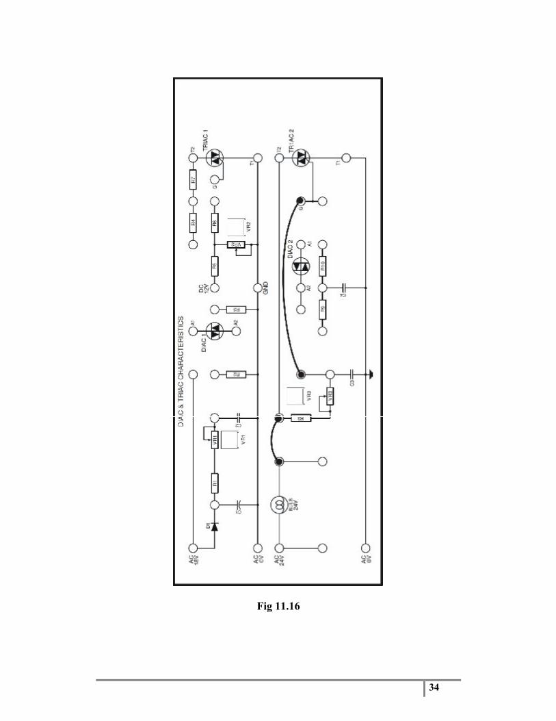
Fig 11.15
33
7. Make connection as in fig 11-15.Connect DC 12V supply from Power Supply unit to Module IT-9000.
8. Set scope to X-Y mode. Connect GND to TRIAC T2 terminal, CH1 input to the other terminal of load R7, and CH2 input to TRIAC T1 terminal. Adjust scope controls to display V-I characteristic curve and plot the curve in Table 11-1.
9. Turning VR2, observe and record the change of V-I characteristic.
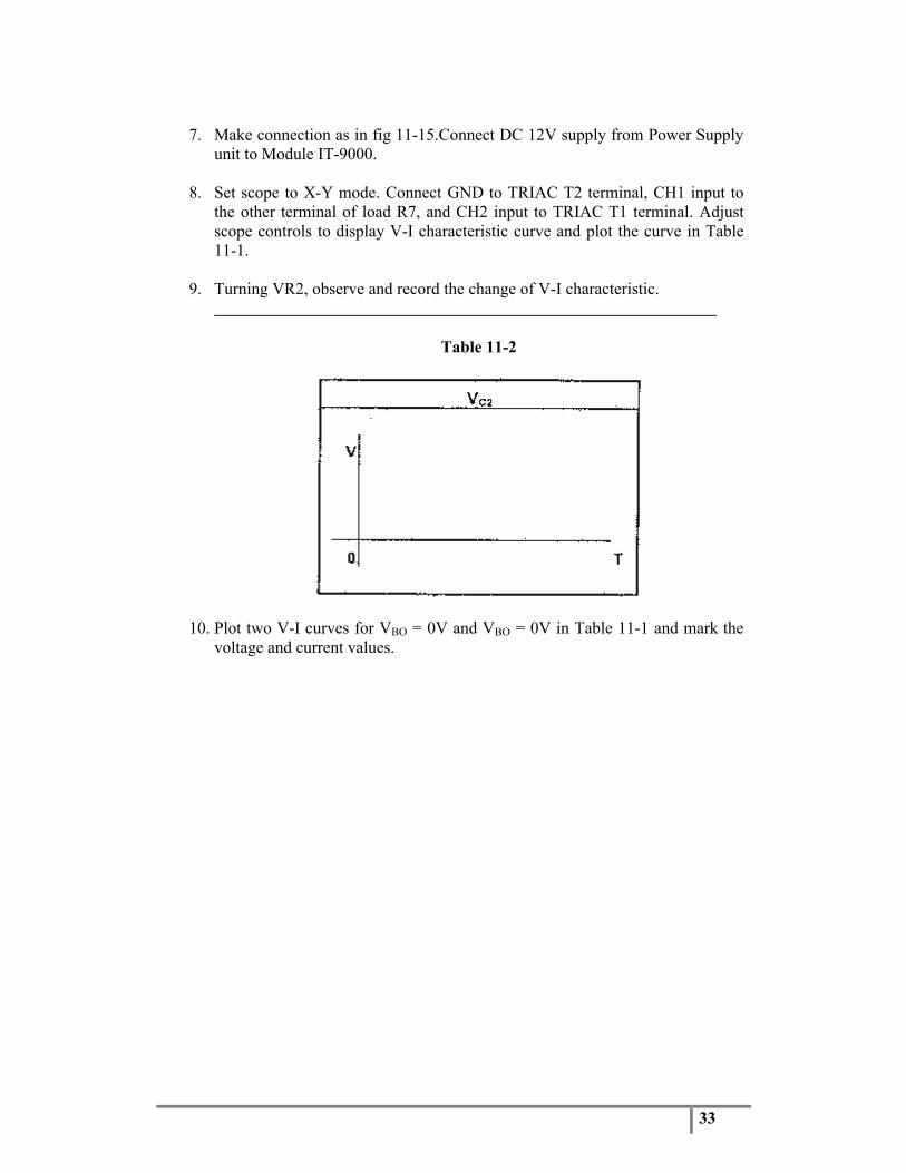
Table 11-2
10. Plot two V-I curves for VBO = 0V and VBO = 0V in Table 11-1 and mark the voltage and current values.
34
Fig 11.16
35
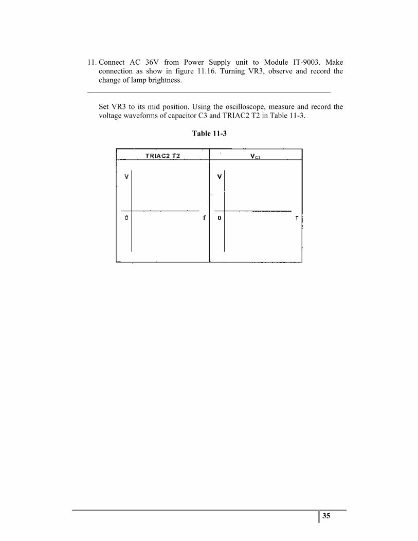
11. Connect AC 36V from Power Supply unit to Module IT-9003. Make connection as show in figure 11.16. Turning VR3, observe and record the change of lamp brightness.
Set VR3 to its mid position. Using the oscilloscope, measure and record the voltage waveforms of capacitor C3 and TRIAC2 T2 in Table 11-3.
Table 11-3
36
Fig 11.17
37
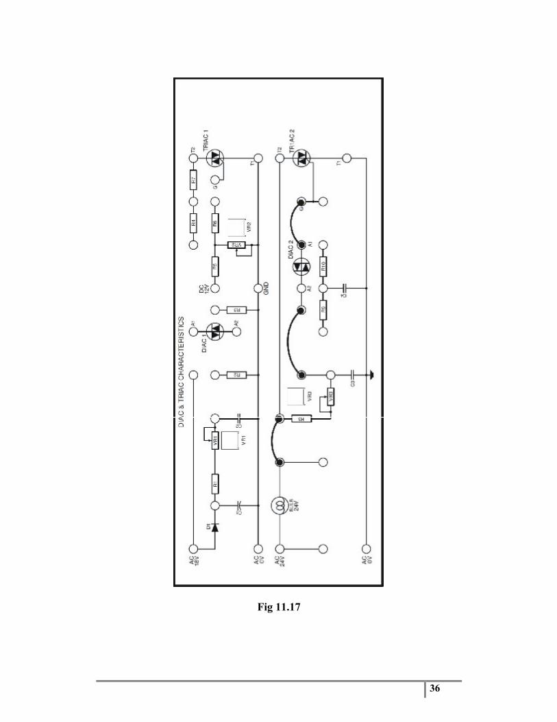
12. Make connection as in fig 11-17. Turning VR3, observe and record the change of lamp brightness.
Set VR3 to its midposition. Using the oscilloscope, measure and record the voltage waveforms of capacitor C3 and TRIAC T2 in Table 11-4.
Table 11-4
38
Fig 11.18
39
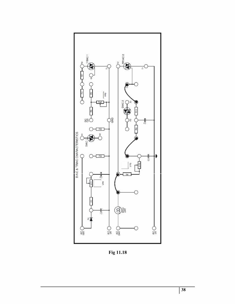
13. Make connection as in fig 11-18. Turning VR3, observe and record the change of lam brightness.
Comparing to the results of step 11, is the hysteresis phenomenon improved?
Set VR3 to its midposition. Using the oscilloscope, measure and record thevoltage waveforms of capacitor C3 and TRIAC2 T2 in Table 11-5.
Table 11-5
Conclusion
In step 2, you have observed the characteristic curve of the DIAC using the oscilloscope. The VP and VV values of DIAC are obtained from the waveform of VC2.
The VR2 is used to adjust the magnitude of the gate voltage of the TRIAC1 for TRIAC characteristic measurement. That is, the greater the VR2 resistance, the greater the gate current becomes.
The operation of the DIAC-TRIAC phase control circuit is similar to SCR phase control circuit. By changing VR3xC3 time constant, the conduction angle of TRIAC2 and the output power on load are regulated. The components R9 and C4 are used to improve the hysteresis phenomenon found in step 11.