Courtesy Michael Konig Date: January 10, 2014 Prepared by: James F. Salzman Product Engineer: Fee-Nee Yap, Mohammad Karim Test Engineering: Bret Dahl, Veeraraghavan Narayanan Design Engineering: Hector Torres, Srinivasan Venkataraman Marketing: Chris Hart Contact: [email protected]Total Ionizing Dose (TID) and Single Event Effects (SEE) Test Report Low Drop Out ( LDO) Regulator TPS7H1101‐SP QMLV SMD#: 5962-1320201VXC James F. Salzman TEXAS INSTRUMENTS
Transcript
Courtesy Michael Konig
Date: January 10, 2014Prepared by: James F. SalzmanProduct Engineer: Fee-Nee Yap, Mohammad KarimTest Engineering: Bret Dahl, Veeraraghavan NarayananDesign Engineering: Hector Torres, Srinivasan Venkataraman Marketing: Chris HartContact: [email protected]
Total Ionizing Dose (TID) and Single
Event Effects (SEE) Test Report
Low Drop Out ( LDO) RegulatorTPS7H1101‐‐‐‐SP QMLV
SMD#: 5962-1320201VXC
James F. Salzman
TEXASINSTRUMENTS
TPS7H1101-SP Product Description
The TPS7H1101-SP is a low dropout (LDO) linear regulator that uses a PMOS pass element. The benefits of this approach is very low dropout, and performance, at higher temperatures and during Single Event Effects (SEE). The TPS7H1101-SP operates over a wide range of input voltage, from 1.5 V to 7 Volts, enabling very low noise regulation in application transitions from 6V-IN to 5 V-OUT, and 1.5 V-IN to 1.2 V-OUT with excellent Power Supply Rejection Ratio (PSRR). It also features a Power Good output for easy power sequencing, and a programmable Current Limit, and Soft Start. The part is available in a 16 pin ceramic flat pack QMLV certified under SMD # 5962-1320201VXC as shown below.
Radiation Executive Test Summary
The TPS7H1101-SP has been radiation tested against Total Ionizing Dose (TID) and Single Event Effects (SEE). This report presents details on the tests performed. In summary the device is very rugged to these effects as shown below:
* Threshold for SET/SEFI detection was set to a +\- 2% change of Vout
QMLV QualifiedCeramic Flat Pack5962-1320201VXC
1.0. TID Overview and Background
It is well known that ionizing radiation can cause parametric degradation and ultimately functional failures in electronic devices. There are two dominant mechanisms associated with these effects, the generation of hole traps and interface states. Both of these mechanisms contribute to the overall MOS transistor Vt shifts. First order effects are typically seen in the thick field isolation region and second order effects in the gate region, under Total Irradiated Dose (TID) exposure. These mechanisms occur due to electron-hole pair production from ionization radiation and their transport and trapping in the dielectric and silicon interface regions. These mechanisms, know as hole traps, “Vot” and interface traps “Vit” have been studied for many years and are well documented. It is also well know that annealing of the these mechanisms can occur over time and may be accelerated by temperature. Figure 1. is a general summary of these effects. The effects are greatly dependent dielectric thickness of the particular process technology node and also device component construction.
.
TPS7H1101-SP QMLV Radiation Report
Figure 1. Vot / Vit Generation and Time/ Temperature Annealing
After J. R. Schwank, et al.,IEEE Trans. Nucl. Sci. NS-
31, 1453 (1984)
Accumulation of hole traps is typically the primary mechanism for increased leakage and failures in MOS semiconductor devices. MOS Semiconductor devices are typically less dependent on the generation of interface traps, but the ratio of these two mechanisms do play a role in overall time dependent device behavior, and are typically very process and structure dependent. The anneal rate of hole traps (either deep or shallow) of a particular device is also process and structure dependent. Some semiconductor processes exhibit quick anneal rates, while others may anneal at a low rates. Activation energy plays an important role in these recombination rates, i.e. annealing of hole traps, as show by elevated temperatures in figure 1. On the other hand interface (electron or H) traps do not anneal easily and can accumulate over time. Because of accelerated testing, both hole traps and interface generation rates may not correlate to the actual intended radiation mission environment. In a space environment the where TID rates are typically less than 0.01mRad/sec, giving way to unexpected results compared to accelerated exposure. MIL-STD-883, method 1019 covers both annealing , and rebound effects ( accelerated anneal) with a 168 hour 100oC post electrical test. Interface state generation is of prime importance for bipolar devices, being one of the major factors in Enhanced Low Dose Rate Sensitivity (ELDRS) of these device. Bipolar structures are affected primarily by interface states and secondary by hole traps in the base oxide. Both of these mechanisms play a role in device behavior. Both again are very process and structure dependent.
Figure 2. TI SVAGamma Cell
The TPS7H1101-SP has been evaluated for TID tolerance. High dose Rate (HDR) exposure was performed on biased and unbiased devices in a Co60 gamma cell at TI SVA facility in Santa Clara California. Figure 2. illustrates a picture of the Gamma Cell 220 used for the exposure. The un-attenuated dose rate of this cell is 100 RAD/sec.
The test matrix of devices is included in Appendix A. After exposure. The devices were packed in dry ice ( per MIL-STD-883H Method 1019.9 section 3.10. ) and returned to TI Dallas for a full post radiation electrical evaluation on Automated Test Equipment (ATE).
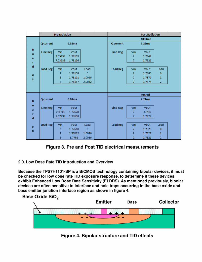
Test conditions for HDR are shown in Figure 3. Measurements include pre-radiation quiescent current, Vin, and load regulation values. Post radiation measurements were taken within 30 minutes of removal of the devices from the dry ice container. The devices were allowed to reach room temperature prior to electrical post radiation measurements. At the 50kRAD TID level, a ~ 6mV Vout delta was observed, while a ~ 10mV Vout delta was observed at the 100kRAD level.
Figure 3. Pre and Post TID electrical measurements
BaseEmitter CollectorBase Oxide SiO2
+ + + + + +- - - - - -
Figure 4. Bipolar structure and TID effects
2.0. Low Dose Rate TID Introduction and Overview
Because the TPS7H1101-SP is a BiCMOS technology containing bipolar devices, it must be checked for low dose rate TID exposure response, to determine if these devices exhibit Enhanced Low Dose Rate Sensitivity (ELDRS). As mentioned previously, bipolar devices are often sensitive to interface and hole traps occurring in the base oxide and base emitter junction interface region as shown in figure 4.
The charge yield or generation rates of hole and interface traps both contribute to overall “effective” Hfe or transistor gain reduction in bipolar transistors. Interface trap generation is often the dominate mechanism effecting bipolar transistor gain. Interface state generation is primarily caused by the proton transport mechanism or the release of trapped hydrogen in the device from processing, particularly in oxide layers. The generation of these interface states are greatly enhanced at low dose rates due to a low concentration of hole traps at the interface that typically repel positive charged hydrogen under high dose rate exposure. The test for low dose rate sensitivity is described in method 1019.9, and is performed at 10mRAD(si)/sec. A rate that is still much higher than actual space dose rates, but is much closer than High Dose Rates (HDR) or the accelerated rates of 50-300RAD/sec called out in Condition A of MIL-STD-883H, 1019.9. This is then compared to HDR for anysubstantial differences with LDR results.
The TPS7H1101-SP Low Drop Out Regulator (LDO) is manufactured in TI’s 7th
generation Linear BiCMOS (LBC7) process technology. Over 99.9% of the design utilizes the CMOS components from the component library in the LBC7 process. The device incorporates only three bipolar transistors that are used in the design of the band gap reference and a 4th device used for current shutdown. As previously mentioned Per Mil-Std-883H, method 1019.9, a BiCMOS technology should be checked for Low Dose Rate (LDR) Total Ionizing Dose (TID) exposure response. The purpose of this test is to determine if there are time dependent effects to dose rate, in particular to low dose rates, in such application as Space where charge yield is low.
The facility and Radiation Source used for LDR exposure was Radiation Assured Devices' Longmire Laboratories, Colorado Springs, CO. Co60 (GB-150) low dose rate source, shown in figure 5. Dosimetry is performed by an Air Ionization Chamber (AIC) traceable to NIST. RAD's dosimetry has been audited by DSCC and RAD has been awarded Laboratory Suitability for MIL-STD-750 and MIL-STD-883 TM 1019.
The dose rate is obtained by positioning the device-under-test at a fixed distance from the gamma cell. The dose rate for this irradiator varies from approximately 50rad(Si)/s close to the rods down to <1mrad(Si)/s at a distance of approximately 4-meters.
Figure 5. Low DoseRate Source
As mentioned above, the TPS7H1101-SP contains only four bipolar transistors in the entire design. Three of these devices form an on-chip band gap voltage reference. A design that is commonly used across the semiconductor industry. A schematic implementation of the band gap used in the TPS7H1101-SP is shown in figure 6.
Figure 6. Schematic of LDO Bipolar Band gap Voltage Reference
Three NPN bipolar transistors are used in the band-gap voltage reference.
The fourth bipolar transistor is used in the current shutdown circuit. The schematic of the current shutdown is shown in Figure 7. As current increases in the resistor string, the voltage drop eventually is large enough for forward bias the base emitter junction of the NPN current shutdown circuit. This circuit is not transistor gain sensitive, and hence, robust to TID effects..
Figure 7. Schematic of LDO current shutdown
Single NPN bipolar transistor used for current shutdown
As shown in figure 7, the resistor ladder , Rlad, is across the base emitter junction of the NPN current shutdown transistor. As current increases in the resistor ladder, at a set current point, the voltage drop becomes large enough to turn on the NPN transistor. i.e. forward bias the base-emitter junction. This transistor acts like a switch and triggers the Schmitt buffer, providing a logic like output . The output of the Schmitt buffer causes shutdown of the LDO, and if a proper load is sensed, the LDO will restart. The transistor in this switch configuration is not gain sensitive and therefore robust against TID effects.
Resis
tor
Ladder
Rlad
Low dose rate (LDR) and high dose rate (HDR) testing was performed on a previous silicon revision of the TPS7H1101-SP LDO regulator. Devices were exposed to TID of levels, 10, 20, 30, 40, 50kRAD(si) and checked for both high dose and low dose rate sensitivity at the exposure rate of 50 RAD/(si)sec. and 10mRAD(si)/sec. respectively. No noticeable difference was observed between the High Dose Rate (HDR) and the Low Dose Rate (LDR) data. This initial look ahead radiation testing was used to determine if any changes were needed to the final silicon design. The band gap design did not change from the initial to the final device release.
Qualification TID testing was also performed for final product qualification and has been completed on the LDO. This TID testing includes HDR, LDR in both biased and unbiased configurations to levels of 50-100kRAD(si). The results are shown in figures 4-9 under various Vin and Vout conditions. It should be noted that the observed delta between the 5 configurations in both biased and unbiased conditions after HDR and LDR showed little change. All units used in the radiation qualification exposure were from the same wafer lot, used the same production packaging, and went through burn-in prior to TID exposure. Post radiation accelerated anneal showed no potential long term effects.
It should be noted that any change in the band gap characteristics will cause an output voltage change, or Vout voltage change. Also any circuit behavior changes would also alter the regulation of the regulator. No noticeable changes were observed after the above HDR and LDR data logs. The NPN transistors used in this design, showed no sensitivity to TID dose rate.
In conclusion the device does not exhibit ELDRS, and is targeted to be released as a 100kRAD(si) RHA product in 1Q2014.
Figure 4. HDR/LDR delta Vout Measurements
Figure 5. HDR/LDR delta Vout Measurements
Figure 6. HDR/LDR delta Vout Measurements
Figure 7. HDR/LDR delta Vout Measurements
Figure 8. HDR/LDR delta Vout Measurements
Figure 9. HDR/LDR delta Vout Measurements
3.0 Single Event Effects Testing
Single Event Effects comprises a large group of terms and effects from single or multiple particle events such as those from Neutrons, Protons, and Heavy Ions. Circuit test conditions must be adjusted for various test conditions, along with particle energy, mass, flux, and fluence.
Two separate Heavy ion tests have been completed on the TPS7H1101-SP, one on December 3, 2012, and the second one that took place on November 11, 2013. Both were conducted at the TAMU Cyclotron. The test board used during both tests is shown below in Figure 10.
Vin
Vout Figure 10. EVM Board used for SEE testing
The complete EValuation Module ( EVM ) is attached as appendix A, including schematics. Input capacitor to the LDO was an onboard total of 100uF, while the output capacitance of the LDO was 220uF. The output voltage was set by changing out R27. With R27 set at 10K the output voltage was 1.2Volts, and with R27 set at 20K, the output voltage was 1.8 Volts. The feedback/voltage set divider can be found in Appendix A.
TPS7H1101-SP DUT,Metal lid removed during testing.
Cin = 100uF
Cout = 220uF
R28 = 10K
R27 = 10K
R27 = 20K
3.1 Single Event Effects Testing ( 1st round )
The TPS7H1101-SP was evaluated against Heavy Ion exposure from the Texas A&M University 88-inch Cyclotron on December 3, 2012. A 15 MeV/amu beam line was used with the ions shown in table 1. The LET show below was an effective LET measurement from the beam line equipment. Zero degree “ incident” and 45 degree angles were used to vary the effective LET on the three selected ions in Table 1. Available beam characteristics are show in Figure 11.
Ion Total Energy (MeV) LET (MeV-cm2/mg) Range in Si (µm)
84Kr 1259 28.2 170
129Xe 1934 52.1 156
165Ho 2475 69.8 112
Table 1. Heavy ion selection
Figure 11. TAMU Cyclotron 15 A MeV Beam Characteristics
The TPS7H1101-SP Heavy Ion Run Log is show in Table 2. LET ion values range from~ 28 MeV-cm2/mg to 100 MeV-cm2/mg. SET events were defined as Vout changes of
>10%, while SEFI events were determined by a logic level transition of the Power Good (PG) signal.
Table 2. Heavy Run Log
3.2 Single Event Effects Run Log
The TPS7H1101-SP was SEE tested under various Vin and Vout conditions, as well as load conditions of 0A – 3A load. The external filter capacitor value used was 220uF. SEL and SEB testing included maximum input voltage of 7V @ room and at 125oC, as well as high and low Vout values. Total fluence for each of these runs reached 1E7 ions/cm2
using 165Ho ion at a 45 degree angle, providing an effective LET ~ 100 MeV-cm2/mg
No SET or SEFI’s were observed at LET < 40 MeV-cm2/mg. The first observable event was using 129Xe with an effective LET ~ 52 MeV-cm2/mg. Onset LET is somewhere between 40 and 52 MeV-cm2/mg. This suggests the device is immune to a LEO proton environment.
Figure 12 is a cross section plot of SET and SEFI events combined. The saturated cross section approaches 1.0E-04 cm2. Figure 13 illustrates a SET event, where a Vout change of > 10% occurs causing the trigger of the Power Good signal. Figure 13 illustrates a SEFI event triggering a soft start event.
Figure 12. Weibull Cross Section Fit
Effective LET in MeV-cm2/mg
Figure 13. SEFI Producing Soft Start event
Figure 12. SET causing Power Good Signal Transition
4.0 Single Event Effects ( 2nd round )
The TPS7H1101-SP was evaluated against Heavy Ion exposure from the Texas A&M University 88-inch Cyclotron on November 11, 2013 to collect additional heavy ion data around the onset threshold of 40 MeV-cm2/mg. The trigger point for detecting upsets was lowered to 5% and 2% of Vout rather than 10%, and any positive transients of Vout was monitored. There were no upsets observed below the 40 MeV-cm2/mg onset threshold at either a 2% or 5% change of Vout.
The 15 MeV/amu beam line was used with the ions shown in table 3. The LET show below was an effective LET measurement from the beam line equipment. Zero degree “ incident” and 45 degree angles were used to vary the effective LET on the two selected ions in Table 3.
Ion Total Energy (MeV) LET (MeV-cm2/mg) Range in Si (µm)
84Kr 1259 28.8 170
197Au 2954 86.3 155
Table 3. Heavy ion selection
The run log of the November 11th 2013 is shown in Table 4. 84Kr was used at a 45 degree angle and produced an effective LET of 40.7 MeV-cm2/mg. No trigger events were detected at this LET. A 197Au ion was used at the beginning of the test to determine the proper operation of the setup, and did correlate to the previous TAMU tests.
TEST Run Time Distance Temp Ion/LET
Beam
Angle Flux Fluence Vin Vout Load Events Notes
SEU 62 7:00 30mm 25Au/82MeV
01.00E+04 1.00E+06
1.5V 1.2V 2.9A 22 Trigger 5% of Vout, capture SS/PG/Vout
SEU 64 7:26 30mm 25 Kr/40 MeV 451.00E+04 1.00E+06
1.5V 1.2V 3A 0 Trigger 5% of Vout, capture SS/PG/Vout
SEU 65 7:29 30mm 25 Kr/40 MeV 451.00E+04 1.00E+06
1.5V 1.2V 3A 0 Trigger 2% of Vout, capture SS/PG/Vout
During the 2nd round of SEE testing the output was again checked for any positive going SET events. ( This is where the output will go higher than the set point of Vout. ) No positive going transients were observed. The detection trigger point of Vout was set to +\-5% and then +\- 2% delta Vout. No observed SET/SEFI ‘s were observed at or below the onset threshold of 40.7Mev-cm2/mg. At higher LET’s only negative going SET/SEFI events were observed. ( a droop in Vout )
In order to upset high, the gate of the PMOS pass element during SET must be pulled down. The design uses an asymmetrical gate driver for the PMOS pass element. i.e. The driver can source a lot more current than it is able to sink. If you pull down the input of the gate driver there is a time constant associated with slewing or drawing down the gate charge of the pass element. This time is dictated by a fixed pull down current source and the overall gate capacitance of the pass element (I/C = dV/dt). The time needed to discharge significant gate charge ( the voltage ) is much greater than the time duration of our modeled critical charge produced for a LET of 85 MeV-cm2/mg. This means that the charge injection associated with a heavy ion strike producing a LET of 85 MeV-cm2/mg is of insufficient time duration to cause a significant droop on the gate voltage (not enough charge is removed from the equivalent gate capacitance). A strike on the output of the gate driver also meets a similar fate as there is simply not enough charge removed from the gate capacitance to cause a SET. This is the reason we don’t see SET events going high during Single Event testing.
It should be noted though, that large inductive loads may produce a back EMF that will push the output of the LDO high. The LDO has limited current sink capabilities, nor crowbar capability when the output is forced higher than the Vout set point. The LDO is ideally suited for radiation applications such as Medical and Industrial X-Ray, nuclear power plants, high altitude avionics, and space.
5.0 Summary
During the 1st round of SEE testing It was determined that there were no upsets on Vout with the Vout threshold trigger set at +\- 10% delta Vout at or below the onset threshold of 40.7 MeV-cm2/mg. No trigger events were detected at this LET, which verified previous SET testing that showed no upsets at a LET of < 40.7 MeV-cm2/mg.
Appendix A
IMPORTANT NOTICE
Texas Instruments Incorporated and its subsidiaries (TI) reserve the right to make corrections, enhancements, improvements and otherchanges to its semiconductor products and services per JESD46, latest issue, and to discontinue any product or service per JESD48, latestissue. Buyers should obtain the latest relevant information before placing orders and should verify that such information is current andcomplete. All semiconductor products (also referred to herein as “components”) are sold subject to TI’s terms and conditions of salesupplied at the time of order acknowledgment.TI warrants performance of its components to the specifications applicable at the time of sale, in accordance with the warranty in TI’s termsand conditions of sale of semiconductor products. Testing and other quality control techniques are used to the extent TI deems necessaryto support this warranty. Except where mandated by applicable law, testing of all parameters of each component is not necessarilyperformed.TI assumes no liability for applications assistance or the design of Buyers’ products. Buyers are responsible for their products andapplications using TI components. To minimize the risks associated with Buyers’ products and applications, Buyers should provideadequate design and operating safeguards.TI does not warrant or represent that any license, either express or implied, is granted under any patent right, copyright, mask work right, orother intellectual property right relating to any combination, machine, or process in which TI components or services are used. Informationpublished by TI regarding third-party products or services does not constitute a license to use such products or services or a warranty orendorsement thereof. Use of such information may require a license from a third party under the patents or other intellectual property of thethird party, or a license from TI under the patents or other intellectual property of TI.Reproduction of significant portions of TI information in TI data books or data sheets is permissible only if reproduction is without alterationand is accompanied by all associated warranties, conditions, limitations, and notices. TI is not responsible or liable for such altereddocumentation. Information of third parties may be subject to additional restrictions.Resale of TI components or services with statements different from or beyond the parameters stated by TI for that component or servicevoids all express and any implied warranties for the associated TI component or service and is an unfair and deceptive business practice.TI is not responsible or liable for any such statements.Buyer acknowledges and agrees that it is solely responsible for compliance with all legal, regulatory and safety-related requirementsconcerning its products, and any use of TI components in its applications, notwithstanding any applications-related information or supportthat may be provided by TI. Buyer represents and agrees that it has all the necessary expertise to create and implement safeguards whichanticipate dangerous consequences of failures, monitor failures and their consequences, lessen the likelihood of failures that might causeharm and take appropriate remedial actions. Buyer will fully indemnify TI and its representatives against any damages arising out of the useof any TI components in safety-critical applications.In some cases, TI components may be promoted specifically to facilitate safety-related applications. With such components, TI’s goal is tohelp enable customers to design and create their own end-product solutions that meet applicable functional safety standards andrequirements. Nonetheless, such components are subject to these terms.No TI components are authorized for use in FDA Class III (or similar life-critical medical equipment) unless authorized officers of the partieshave executed a special agreement specifically governing such use.Only those TI components which TI has specifically designated as military grade or “enhanced plastic” are designed and intended for use inmilitary/aerospace applications or environments. Buyer acknowledges and agrees that any military or aerospace use of TI componentswhich have not been so designated is solely at the Buyer's risk, and that Buyer is solely responsible for compliance with all legal andregulatory requirements in connection with such use.TI has specifically designated certain components as meeting ISO/TS16949 requirements, mainly for automotive use. In any case of use ofnon-designated products, TI will not be responsible for any failure to meet ISO/TS16949.
Products ApplicationsAudio www.ti.com/audio Automotive and Transportation www.ti.com/automotiveAmplifiers amplifier.ti.com Communications and Telecom www.ti.com/communicationsData Converters dataconverter.ti.com Computers and Peripherals www.ti.com/computersDLP® Products www.dlp.com Consumer Electronics www.ti.com/consumer-appsDSP dsp.ti.com Energy and Lighting www.ti.com/energyClocks and Timers www.ti.com/clocks Industrial www.ti.com/industrialInterface interface.ti.com Medical www.ti.com/medicalLogic logic.ti.com Security www.ti.com/securityPower Mgmt power.ti.com Space, Avionics and Defense www.ti.com/space-avionics-defenseMicrocontrollers microcontroller.ti.com Video and Imaging www.ti.com/videoRFID www.ti-rfid.comOMAP Applications Processors www.ti.com/omap TI E2E Community e2e.ti.comWireless Connectivity www.ti.com/wirelessconnectivity